Download - CBC chip: status and plans - HEP Group

1
Outline
CBC1: first prototype and results summary
current status: CBC2
future plans
Phase 2 Outer Tracker Modules Review, March 2013, Mark Raymond
CBC chip: status and plans

2
LHC -> HL-LHC
8.1 mm 4 mm
APV25
CBC1
rad-hard 0.25um CMOS
unsparsified analogue readout
~ 3 mW / chan for 10-20 cm strips
analogue off-detector transmission
• digital off-detector links
• many more channels -> power
becomes the big issue
130 nm CMOS
unsparsified binary readout
(retain system simplicity but give up analog info)
target low-power for short strips
digital header
128 analogue samples
APV O/P Frame
20 Ms/s readout -> 7 ms
volts
4.54.03.53.02.52.01.51.00.50.0
msec
1 fC signal
injected on
one channel
1st header 2nd header
CBC O/P data - 2 consecutive triggers
128x256
digital
pipeline
12
8 a
mp
. +
co
mp
ara
tor
sh
ift
reg
. O
/P

features
• designed for short strips, 2.5 – 5cm, < ~ 10 pF
• full size prototype - 128 channels
50 mm pitch wirebond
• binary un-sparsified triggered readout only
• powering test features
2.5 -> 1.2 DC-DC converter
LDO regulator (1.2 -> 1.1) feeds analog FE
main functional blocks
• fast front end amplifier – 20 nsec peaking
• comparator with programmable threshold trim
• 256 deep pipeline (6.4 us)
• 32 deep buffer for triggered events
• fast (SLVS) and slow (I2C) control interfaces
some target specs
• both signal polarities
• DC coupled to sensor – up to 1 uA leakage
• noise: < 1000e for CSENSOR ~5 pF
• power consumption
< 0.5 mW/channel for CSENSOR ~ 5 pF
data clock
trigger
I2C, reset
7 mm
4 mm
am
pli
fiers
& c
om
para
tors
256 deep
pipeline
+ 32 deep
buffers
bias
generator
2.5 -> 1.25 DC-DC converter
LDO
bandgap
SLVS
power
power
TEST
DEVICES
CBC1
first chips received Feb. 2011 3
Lawrence Jones (RAL)

measured performance
preamp: leakage tolerance 1mA verified, both polarities
postamp: gain: ~ 50 mV / fC
80f 1p
VPLUS
Vdda
16k
200k
100f
60k 92k
115k
VCTH 2k
4k
8k
16k
500k
preamp
postamp
comparator
100
80
60
40
20
0
nu
mb
er
of
eve
nts
600500400300200
comparator threshold VCTH [mV]
1 fC
8 fC
s- curves: signals in range 1 - 8 fC:1 fC steps
noise
1200
1000
800
600
400
200
0
nois
e [
rms e
lectr
ons]
121086420
external capacitance [pF]
400
350
300
250
200
150
100
pow
er p
er c
hannel [u
W]
holes mode
noisepower
noise dependence on external C
vary current in input device
=> pulse shape independent of C
e.g. for CSENSOR ~ 8 pF (~ 5 cm strips)
~ 1000e achievable for
~ 350 uW tot. power/chan. (incl.digital) 4

5
720700680660640
720700680660640
comparator
eve
nts
ab
ove
th
resh
old
comparator global threshold [mV]
128 channels
before tuning
after
threshold uniformity
VDDA
postamp O/P
O/S adjust
8-bit value
(per channel)
16k VCTH
hysteresis
2k
4k
8k
16k
16k
500k
postamp
O/P
thresholds
before tuning pk-pk threshold spread ~30 mV (~ 0.6 fC)
tuning reduces spread to ~ mV level
timewalk
timewalk spec.: < 16 ns between 1.25 and 10 fC
signals, with comp. threshold set to 1 fC
measurements just within spec.
comparator
tim
ew
alk
[ 1
nsec /
div
isio
n ]
109876543210
charge injected [fC]
added capacitance 1.8 pF 3.8 pF 5.8 pF 8.1 pF 10.7 pF
timewalk: threshold at 1 fC
VCTH
6
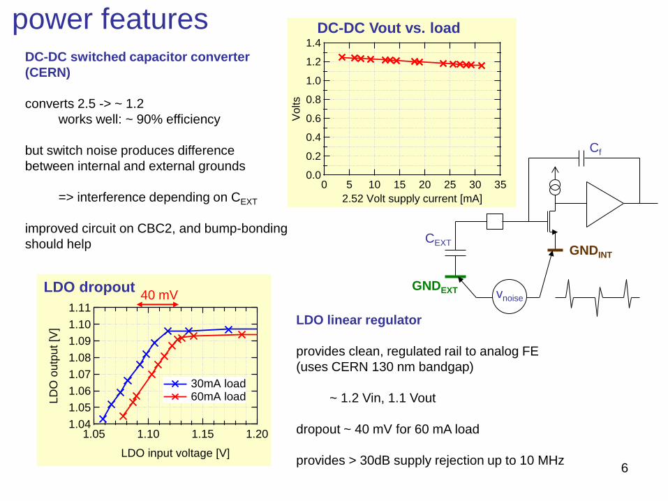
power features DC-DC switched capacitor converter
(CERN)
converts 2.5 -> ~ 1.2
works well: ~ 90% efficiency
but switch noise produces difference
between internal and external grounds
=> interference depending on CEXT
improved circuit on CBC2, and bump-bonding
should help
1.11
1.10
1.09
1.08
1.07
1.06
1.05
1.04
LD
O o
utp
ut [V
]
1.201.151.101.05
LDO input voltage [V]
30mA load 60mA load
LDO dropout 40 mV
GNDEXT
GNDINT CEXT
Cf
vnoise
1.4
1.2
1.0
0.8
0.6
0.4
0.2
0.0
Volts
35302520151050
2.52 Volt supply current [mA]
DC-DC Vout vs. load
LDO linear regulator
provides clean, regulated rail to analog FE
(uses CERN 130 nm bandgap)
~ 1.2 Vin, 1.1 Vout
dropout ~ 40 mV for 60 mA load
provides > 30dB supply rejection up to 10 MHz

7
CBC1 summary
• successful first prototype in 130 nm
most things worked - some bugs needed workarounds (front end CM stability issues)
• learned some valuable information
e.g. performance vs. power trade-offs
<1000e achievable for < 5 mW / channel (target specifications achieved)
• performance verified in test beam
• in the meantime... (2011 - 12)
2S-pT module concept developing
ideas for implementing triggering functionality from strips in outer tracker
ideas on simplifying module construction (bump-bonding)
-> CBC2

8 8
CBC2 for 2S-Pt module
CBC2
bump-bond chip, brings signals from 2 sensor layers in 1 chip (254 channels total)
provides L1 triggered readout data as in prototype
also performs cluster correlations to identify high Pt stub
positive correlation produces trigger output
=> functionality required to construct and evaluate prototype 2S-Pt module
2S (Strips-Strips) module
- 16 readout chips
- each reads 127 strips from bottom sensor
and 127 from top

9
CBC2 architecture
pipe. control
FE amp comp. pipeline shift reg.
vth
vth
vth
vth
256 deep
pipeline
+
32 deep
buffer
test
pulse
bias
gen.
fast
control
slow control
stu
b s
hift re
gis
ter
offse
t co
rre
ction
& c
orr
ela
tio
n
clu
ste
r w
idth
dis
crim
ina
tion
1
254 40 MHz diff.clock
all signals in blue are
single-ended -only travel short
distance on hybrid
trig’d data out
stub shift reg. O/P
trigger O/P
I2C
front end, pipeline, L1 triggered readout, biasing
~ same as prototype (some bug fixes) twice as many channels
new blocks associated with Pt stub generation
channel mask: block problem channels (not from L1 pipeline)
cluster width discrimination: exclude wide clusters > 3
offset correction and correlation: correct for phi offset across module and correlate between layers
stub shift register: test feature - shift out result of correlation operation at 40 MHz
trigger O/P: in normal operation 1 bit per BX indicates presence of high Pt stub
test pulse
charge injection to all channels (8 groups of ~32), programmable timing and amplitude
nearest neighbour signals
T1 trigger
fast reset
test pulse
I2C refresh
4 4 11 11
ch
an
. m
ask
4 4 11 11
nearest neighbour signals
reset
OR_254
OR_stubs
Ck

10 10
stub finding logic
r f
beam
offset window
width
top layer clusters
bottom layer clusters
zero
offset cluster width discrimination (CWD) logic
exclude clusters with hits in >3 neighbouring channels
wide clusters not consistent with high pT track
offset correction & correlation logic
for a cluster in bottom layer, look for correlating cluster occurring
in window in top layer
window width controls pT cut
stub found if cluster in bottom layer corresponds to
cluster within window in top layer
window width programmable up to +/- 8 channels
offset defines lateral displacement of window across chip
programmable up to +/- 3 channels
n
n+1
n-1
1/2/3 strip
cluster on
channel n
programme cluster
width to accept
channel
comparator
outputs
CWD logic

11 11
C4 layout, 250um pitch, 19 columns x 43 rows
30 interchip signals (15 in, 15 out), top and bottom
gives continuity across chip boundaries
right-most column wire-bond (for wafer probe test)
access to:
power
fast control
I2C
outputs
prototype powering features retained
CERN bandgap, LDO for analog powering, same as prototype
improved DC-DC switched capacitor circuit (CERN)
slower switching edges & rad-hard layout
chip submitted for fabrication July 2012
wafers back January 2013
DC
-DC
LDO
pipeline
+
buffering
25
4 a
mp
lifi
er/
co
mp
ara
tor
ch
an
ne
ls
CW
D,
off
se
t c
orr
ec
tio
n a
nd
co
lle
ralt
ion
lo
gic
ba
nd
ga
p
bia
s g
en
.
254
inputs
CBC2 layout 5 mm
11
mm
inter-
chip
signals
inter-
chip
signals
Davide Braga,
Mark Prydderch,
Peter Murray
(RAL)

12
notch
wafer name:
A4PNFAH
CBC2
reticle
CBC2 C4 wafers

13 13
wirebond CBC2 test setup
LVDS signal levels
3.3V I2C
use wafer probe pads to wirebond single CBC2 die to carrier
(CBC2 chips from diced wire-bond (XFEL) wafer)
convenient setup for developing detailed wafer probe procedures
power power
power VME based
DAQ

14
first result
1
2
3
4
5
6
7
8
9
10
11
12
13
14
15
16
17
18
19
20
21
22
23
1
1
2
2
3
3
4
4
5
5
6
6
7
7
8
8
9
9
10
10
11
11
12
channel
on chip
channel
on layer 1
channel
on layer 2 8 test
groups
arrangement of 8 groups of test pulse connections allows to simulate
signals from different layers and therefore exercise correlation logic
can also verify correlation window width using channel mask register
and window offset
=> chip is working

15
100
80
60
40
20
0
no.
of
events
210200190180170160150140130
VCTH [I2C register setting]
before tuning after tuning
S-curves and tuning
254 S-curves measured with on-chip
test pulse
S-curve mid-points tuned to VCTH
setting of 180
CBC2 channel no.
I2C
va
lue
254 offset values after tuning

16
CBC2 qualitative observations
emphasis so far on verifying functionality - no detailed study
=> have spent most time preparing basic wafer probe test
what can be said so far?
no signs of instability => fixes have worked
power consumption seems “about right”
LDO functioning as expected
2.5 -> 1.2 DC-DC converter also functioning
correlation and window logic verified as far as possible
detailed studies may yet show undesirable features, but chip almost certainly
working well enough to allow module development to progress

17
first wafer probed manually

18
wafer test procedure
check all
channels
respond to
test pulse
power consumption recorded
chip clocked at 40MHz
I2C parameters downloaded power consumption dependence
on I2C value for some bias
currents swept
not an exhaustive test - but should be enough to
differentiate bump-bond assembly problems from
chip problems

19
CBC2
bad chip 112 reticles
108 good chips
4 bad chips
reticle
final yield for 1st wafer
bad chips due
solely to physical
damage
from
probe
card
supply current
- all chips
no defective channel found on any of
112 chips tested on this first wafer
=> 100% yield
perhaps not too surprising if overall wafer yield
high
CBC2 is relatively small area of reticle
& significant fraction of CBC2 area not
occupied by active circuitry

20
20 20
future plans
CBC2 test
CBC3 design & production
CBC3 test
2013 2014 2015 2016 2017
CBC4 design & production
CBC2 available here
CBC4 test
CBC4 full wafer masks and engineering run
CBC2-based module studies
CBC3-based module studies
CBC2 (and modules based on CBC2) will dominate test activity over next ~ 2 years
next prototype, CBC3, should be very close to final chip – available towards end 2014
incorporate functionality to generate and transmit stub addresses
… new features
CBC4 pre-production iteration (2015/16) allows final bug fixes before full-wafer engineering run in 2017
~ 5 years assumed for large scale production, module construction, integration, commissioning, …

21 21
CBC3 - the “final prototype”
bottom
top
8 bits to describe cluster
address in bottom layer
5 bits to describe correlating cluster
address in top layer window
1 or 3 strip
cluster centred
on channel n
2 strip cluster
centred on
n and n+1
n
n+1
n-1
next version of chip should incorporate all features required for HL-LHC
• final choices for front end
½ strip cluster resolution
2 strip cluster position assigned to mid-point
• stub data definition
8 bits address (for ½ strip resolution) of cluster in bottom layer
5 bit bend information
address of correlating cluster in top layer
• stub data formatting & transmission to concentrator
13 bit / stub, up to 3 stubs/BX => 39 bits
+1 bit unsparsified L1 triggered readout data
=> 40 bits / 25 nsec
e.g. 10 lines at 160 Mbps (per chip)
• other useful features
e.g. slow ADC to monitor bias levels
…
concentrator
10 lines / CBC 25 ns
S1 S1 S1 S1 S1 S1 S1 S1 B1 B1
B1 B1 B1 S2 S2 S2 S2 S2 S2 S2
S2 B2 B2 B2 B2 B2 S3 S3 S3 S3
S3 S3 S3 S3 B3 B3 B3 B3 B3 R
25 ns
CBC data to concentrator

22 22
recent developments
• up to now have assumed max. L1 latency of 6.4 usec and L1 accept rate 100 kHz
constraints originate in ECAL readout electronics
• ECAL now considering FE board replacement – removing these constraints
• can we increase latency on CBC?
factor 4 increase seems feasible ~25 usec
denser pipeline layout should mean chip doesn’t need to grow
(much)
longer latency beneficial for L1 data processing
• can we increase trigger rate capability (500 kHz?, 1 MHz?)
wider implications for architecture
at ~ 500 kHz unsparsified readout data dominates available
off-module bandwidth
no room left for stub data
at 1 MHz sparsification becomes unavoidable
where to do it? front end chip? concentrator?
D.Braga (RAL)

23 23
summary
• CBC2 early test results look promising
appears to be working well enough to allow progress with module development
subtleties of performance will become clear when chips are bump-bonded
dual CBC2 substrates (Georges Blanchot)
• substantial test effort
chip: performance vs. temperature, radiation, powering scheme, …
module: performance in lab and test beam
mini-module using dual CBC2, and full-size 8-chip substrates
• further CBC development plans matched to large scale tracker construction effort beginning ~ 2017
CBC3 should be final prototype
ongoing effort to finalise specs., functionality and interfaces
submission mid 2014

24
extra

CBC1 test beam in 2012: Oct. 8th - 22nd
beam tracking plane
using APV
scintillator
CBC + Infineon
sensor box
400 GeV protons
25
MPV = 3.1fC
𝜎 = 0.7 fC
CBC prototype + Infineon
sensor (Vienna)
300 um thick, p-on-n
5cm long strips, 80 um pitch
close to dimensions
proposed for 2S-Pt modules

26
LVDS
signal
levels
3.3V I2C
power
dual-CBC2 substrate interface board
PA charge inject
dual-CBC2 substrate test setup
2xCBC substrate + PA (both sides) becomes device under test
pluggable charge inject board allows different external capacitance

27
front end architecture
80f 1p
VPLUS
Vdda
16k
200k
100f
60k 92k
115k
VCTH 2k
4k
8k
16k
16k
500k
preamp
postamp
comparator
preamp
resistor feedback absorbs ILEAK
works with both sensor polarities
electrons: single 200k resistor
holes: T-network (equiv to 200k)
RfCf implements short 20ns time constant (no pile-up issues)
postamp
AC coupled removes DC shift from leakage current
provides gain: ~50 mV / fC at comparator input
individually programmable O/P DC level implements
channel threshold tuning
comparator
global threshold VCTH
programmable hysteresis
0.66
0.64
0.62
0.60
Vo
lts
400350300250200150100500
time [ns]
0.1 uA 1.1 uA 2.1 uA 3.1 uA 4.1 uA 5.1 uA
simulated post-amp output pulse


