
Rev. 1.1
CMOS 16-BIT SINGLE CHIP MICROCONTROLLER
S1C17611Technical Manual

© SEIKO EPSON CORPORATION 2011, All rights reserved.
NOTICENo part of this material may be reproduced or duplicated in any form or by any means without the written permission of Seiko Epson. Seiko Epson reserves the right to make changes to this material without notice. Seiko Epson does not assume any liability of any kind arising out of any inaccuracies contained in this material or due to its application or use in any product or circuit and, further, there is no representation that this material is applicable to products requiring high level reliability, such as medical prod-ucts. Moreover, no license to any intellectual property rights is granted by implication or otherwise, and there is no representation or warranty that anything made in accordance with this material will be free from any patent or copyright infringement of a third party. This material or portions thereof may contain technology or the subject relating to strategic products under the control of the Foreign Exchange and Foreign Trade Law of Japan and may require an export license from the Ministry of Economy, Trade and Industry or other approval from another government agency.
This product uses SuperFlash® technology licensed from Silicon Storage Technology, Inc.All brands or product names mentioned herein are trademarks and/or registered trademarks of their respective companies.

DevicesS1 C 17xxx F 00E1
Packing specifications00 : Besides tape & reel0A : TCP BL 2 directions0B : Tape & reel BACK0C : TCP BR 2 directions0D : TCP BT 2 directions0E : TCP BD 2 directions0F : Tape & reel FRONT0G: TCP BT 4 directions0H : TCP BD 4 directions0J : TCP SL 2 directions0K : TCP SR 2 directions0L : Tape & reel LEFT0M: TCP ST 2 directions0N : TCP SD 2 directions0P : TCP ST 4 directions0Q: TCP SD 4 directions0R : Tape & reel RIGHT99 : Specs not fixed
Specification
PackageD: die form; F: QFP, B: BGA
Model number
Model nameC: microcomputer, digital products
Product classificationS1: semiconductor
Development toolsS5U1 C 17000 H2 1
Packing specifications 00: standard packing
Version 1: Version 1
Tool typeHx : ICEDx : Evaluation boardEx : ROM emulation boardMx: Emulation memory for external ROMTx : A socket for mounting
Cx : Compiler packageSx : Middleware package
Corresponding model number17xxx: for S1C17xxx
Tool classification C: microcomputer use
Product classification S5U1: development tool for semiconductor products
00
00
Configuration of product number
CONTENTS
S1C17611 TECHNICAL MANUAL Seiko Epson Corporation i
- CONTENTS -
1 Overview ........................................................................................................................1-11.1 Features ...........................................................................................................................1-2
1.2 Block Diagram ..................................................................................................................1-3
1.3 Pins ..................................................................................................................................1-4
1.3.1 Pinout Diagram ..................................................................................................1-41.3.2 Pin Descriptions .................................................................................................1-7
2 CPU ................................................................................................................................2-12.1 S1C17 Core Features ......................................................................................................2-1
2.2 CPU Registers .................................................................................................................2-2
2.3 Instruction Set ..................................................................................................................2-3
2.4 Vector Table ......................................................................................................................2-70x5328–0x532a: Vector Table Address Low/High Registers (MISC_TTBRL, MISC_TTBRH) ... 2-7
2.5 PSR Readout ...................................................................................................................2-80x532c: PSR Register (MISC_PSR).......................................................................................... 2-8
2.6 Processor Information ......................................................................................................2-90xffff84: Processor ID Register (IDIR) ....................................................................................... 2-9
3 Memory Map and Bus Control .....................................................................................3-13.1 Bus Cycle .........................................................................................................................3-2
3.1.1 Access Size Restrictions....................................................................................3-23.1.2 Instruction Execution Cycle Restrictions ............................................................3-2
3.2 Flash Area ........................................................................................................................3-3
3.2.1 Internal Flash Memory .......................................................................................3-33.2.2 Flash Memory Programming .............................................................................3-33.2.3 Protect Bits ........................................................................................................3-3
0xfffc–0xfffe: Flash Protect Bits ................................................................................................. 3-4
3.2.4 Flash Controller Access Control ........................................................................3-40x5320: FLASHC/SRAMC Control Register (MISC_FL) ........................................................... 3-4
3.3 Internal RAM Area............................................................................................................3-5
3.3.1 Internal RAM ......................................................................................................3-50x5326: IRAM Size Select Register (MISC_IRAMSZ) ............................................................... 3-5
3.4 Display RAM Area ............................................................................................................3-6
3.4.1 Display RAM ......................................................................................................3-63.5 Internal Peripheral Circuit Area ........................................................................................3-7
3.5.1 Internal Peripheral Circuit Area 1 (0x4000 onward) ...........................................3-73.5.2 Internal Peripheral Circuit Area 2 (0x5000 onward) ...........................................3-7
3.6 Core I/O Reserved Area ...................................................................................................3-8
4 Power Supply Voltage ...................................................................................................4-14.1 Power Supply Voltage .......................................................................................................4-1
4.2 Internal Power Supply Circuit ...........................................................................................4-2
4.3 Power Supply Circuit Control............................................................................................4-3
4.4 Heavy Load Protection Function ......................................................................................4-4
4.5 Control Register Details ...................................................................................................4-50x5120: VD1 Control Register (VD1_CTL) ................................................................................. 4-60x50a3: LCD Voltage Regulator Control Register (LCD_VREG) ............................................... 4-7
4.6 Precautions ......................................................................................................................4-8
5 Initial Reset ...................................................................................................................5-15.1 Initial Reset Factors ..........................................................................................................5-1
5.1.1 #RESET pin .......................................................................................................5-1
CONTENTS
ii Seiko Epson Corporation S1C17611 TECHNICAL MANUAL
5.1.2 P0 Port Key-Entry Reset ....................................................................................5-25.1.3 Reset by Watchdog Timer ..................................................................................5-2
5.2 Initial Reset Sequence .....................................................................................................5-3
5.3 Initial Settings at Initial Resetting .....................................................................................5-4
6 Interrupt Controller (ITC) .............................................................................................6-16.1 ITC Configuration .............................................................................................................6-1
6.2 Vector Table ......................................................................................................................6-2
6.3 Maskable Interrupt Control ...............................................................................................6-3
6.3.1 Peripheral Module Interrupt Control Bit ..............................................................6-36.3.2 ITC Interrupt Request Processing .....................................................................6-36.3.3 S1C17 Core Interrupt Processing ......................................................................6-4
6.4 NMI ...................................................................................................................................6-5
6.5 Software Interrupts ...........................................................................................................6-6
6.6 HALT and SLEEP Mode Cancellation ..............................................................................6-7
6.7 Control Register Details ...................................................................................................6-80x4306: Interrupt Level Setup Register 0 (ITC_LV0) ................................................................. 6-90x4308: Interrupt Level Setup Register 1 (ITC_LV1) ................................................................ 6-100x430a: Interrupt Level Setup Register 2 (ITC_LV2) ................................................................ 6-110x430c: Interrupt Level Setup Register 3 (ITC_LV3) ................................................................ 6-120x430e: Interrupt Level Setup Register 4 (ITC_LV4) ................................................................ 6-130x4310: Interrupt Level Setup Register 5 (ITC_LV5) ................................................................ 6-140x4312: Interrupt Level Setup Register 6 (ITC_LV6) ................................................................ 6-150x4314: Interrupt Level Setup Register 7 (ITC_LV7) ................................................................ 6-160x4316: Interrupt Level Setup Register 8 (ITC_LV8) ................................................................ 6-170x4318: Interrupt Level Setup Register 9 (ITC_LV9) ................................................................ 6-18
6.8 Precautions .....................................................................................................................6-19
7 Oscillator Circuit (OSC) ...............................................................................................7-17.1 OSC Module Configuration ..............................................................................................7-1
7.2 IOSC Oscillator Circuit .....................................................................................................7-2
7.3 OSC3 Oscillator Circuit ....................................................................................................7-3
7.4 OSC1 Oscillator Circuit ....................................................................................................7-5
7.5 Clock Switching ................................................................................................................7-6
7.6 LCD Clock Control............................................................................................................7-8
7.7 8-bit OSC1 Timer Clock Control .......................................................................................7-9
7.8 SVD Clock Control ..........................................................................................................7-10
7.9 RFC Clock Control .........................................................................................................7-11
7.10 Clock External Output (FOUTH, FOUT1) ......................................................................7-12
7.11 RESET and NMI Input Noise Filters ..............................................................................7-14
7.12 Control Register Details ................................................................................................7-150x5060: Clock Source Select Register (OSC_SRC) ................................................................ 7-160x5061: Oscillation Control Register (OSC_CTL) .................................................................... 7-170x5062: Noise Filter Enable Register (OSC_NFEN) ................................................................ 7-190x5063: LCD Clock Setup Register (OSC_LCLK) .................................................................... 7-200x5064: FOUT Control Register (OSC_FOUT) ........................................................................ 7-210x5065: T8OSC1 Clock Control Register (OSC_T8OSC1) ...................................................... 7-220x5066: SVD Clock Control Register (OSC_SVD) ................................................................... 7-230x5067: RFC Clock Control Register (OSC_RFTCK) .............................................................. 7-24
7.13 Precautions ...................................................................................................................7-25
8 Clock Generator (CLG) .................................................................................................8-18.1 Clock Generator Configuration .........................................................................................8-1
8.2 CPU Core Clock (CCLK) Control .....................................................................................8-2

CONTENTS
S1C17611 TECHNICAL MANUAL Seiko Epson Corporation iii
8.3 Peripheral Module Clock (PCLK) Control .........................................................................8-3
8.4 Control Register Details ...................................................................................................8-40x5080: PCLK Control Register (CLG_PCLK) .......................................................................... 8-50x5081: CCLK Control Register (CLG_CCLK) .......................................................................... 8-6
8.5 Precautions ......................................................................................................................8-7
9 Prescaler (PSC) .............................................................................................................9-19.1 Prescaler Configuration ....................................................................................................9-1
9.2 Control Register Details ...................................................................................................9-20x4020: Prescaler Control Register (PSC_CTL) ....................................................................... 9-2
9.3 Precautions ......................................................................................................................9-3
10 Input/Output Port (P) .................................................................................................10-110.1 Input/Output Port Configuration ....................................................................................10-1
10.2 Input/Output Pin Function Selection (Port MUX) ...........................................................10-2
10.3 Data Input/Output ..........................................................................................................10-3
10.4 Pull-up Control ..............................................................................................................10-5
10.5 Input Interface Level ......................................................................................................10-6
10.6 P0 and P1 Port Chattering Filter Function ....................................................................10-7
10.7 Port Input Interrupt ........................................................................................................10-8
10.8 Control Register Details ...............................................................................................10-100x5200/0x5210/0x5220: Px Port Input Data Registers (Px_IN) .............................................. 10-110x5201/0x5211/0x5221: Px Port Output Data Registers (Px_OUT) ....................................... 10-120x5202/0x5212/0x5222: Px Port Output Enable Registers (Px_OEN) .................................... 10-130x5203/0x5213/0x5223: Px Port Pull-up Control Registers (Px_PU) ...................................... 10-140x5204/0x5214/0x5224: Px Port Schmitt Trigger Control Registers (Px_SM)......................... 10-150x5205/0x5215: Px Port Interrupt Mask Registers (Px_IMSK) ............................................... 10-160x5206/0x5216: Px Port Interrupt Edge Select Registers (Px_EDGE) ................................... 10-170x5207/0x5217: Px Port Interrupt Flag Registers (Px_IFLG) .................................................. 10-180x5208/0x5218: Px Port Chattering Filter Control Registers (Px_CHAT) ................................ 10-190x5209: P0 Port Key-Entry Reset Configuration Register (P0_KRST) .................................... 10-210x520a/0x521a/0x522a: Px Port Input Enable Registers (Px_IEN) ........................................ 10-220x52a0: P0 Port Function Select Register (P0_PMUX) ........................................................... 10-230x52a1: P0 Port Function Select Register (P0_PMUX) ........................................................... 10-240x52a2: P1 Port Function Select Register (P1_PMUX) ........................................................... 10-250x52a3: P1 Port Function Select Register (P1_PMUX) ........................................................... 10-260x52a4: P2 Port Function Select Register (P2_PMUX) ........................................................... 10-27
10.9 Precautions ..................................................................................................................10-28
11 16-bit Timer (T16) .......................................................................................................11-111.1 16-bit Timer Overview ...................................................................................................11-1
11.2 16-bit Timer Operating Modes .......................................................................................11-2
11.2.1 Internal Clock Mode ........................................................................................11-211.2.2 External Clock Mode .......................................................................................11-311.2.3 Pulse Width Measurement Mode ....................................................................11-4
11.3 Count Mode ...................................................................................................................11-5
11.4 16-bit Timer Reload Register and Underflow Cycle ......................................................11-6
11.5 16-bit Timer Reset .........................................................................................................11-7
11.6 16-bit Timer RUN/STOP Control ...................................................................................11-8
11.7 16-bit Timer Output Signal ............................................................................................11-9
11.8 16-bit Timer Interrupts ..................................................................................................11-10
11.9 Control Register Details ...............................................................................................11-110x4220/0x4240/0x4260: 16-bit Timer Ch.x Input Clock Select Registers (T16_CLKx) ........... 11-120x4222/0x4242/0x4262: 16-bit Timer Ch.x Reload Data Registers (T16_TRx) ...................... 11-13

CONTENTS
iv Seiko Epson Corporation S1C17611 TECHNICAL MANUAL
0x4224/0x4244/0x4264: 16-bit Timer Ch.x Counter Data Registers (T16_TCx) ..................... 11-140x4226/0x4246/0x4266: 16-bit Timer Ch.x Control Registers (T16_CTLx)............................. 11-150x4228/0x4248/0x4268: 16-bit Timer Ch.x Interrupt Control Registers (T16_INTx) ............... 11-17
11.10 Precautions ................................................................................................................11-18
12 8-bit Timer (T8F) .........................................................................................................12-112.1 8-bit Timer Overview .....................................................................................................12-1
12.2 8-bit Timer Count Mode .................................................................................................12-2
12.3 Count Clock ...................................................................................................................12-3
12.4 8-bit Timer Reload Register and Underflow Cycle ........................................................12-4
12.5 8-bit Timer Reset ...........................................................................................................12-5
12.6 8-bit Timer RUN/STOP Control .....................................................................................12-6
12.7 8-bit Timer Output Signal ..............................................................................................12-7
12.8 Fine Mode .....................................................................................................................12-8
12.9 8-bit Timer Interrupts .....................................................................................................12-9
12.10 Control Register Details .............................................................................................12-100x4200: 8-bit Timer Input Clock Select Register (T8F_CLK) ................................................... 12-110x4202: 8-bit Timer Reload Data Register (T8F_TR) .............................................................. 12-120x4204: 8-bit Timer Counter Data Register (T8F_TC)............................................................. 12-130x4206: 8-bit Timer Control Register (T8F_CTL) .................................................................... 12-140x4208: 8-bit Timer Interrupt Control Register (T8F_INT) ....................................................... 12-16
12.11 Precautions ................................................................................................................12-17
13 PWM Timer (T16E) .....................................................................................................13-113.1 PWM Timer Overview ...................................................................................................13-1
13.2 PWM Timer Operating Modes .......................................................................................13-2
13.3 Setting and Resetting Counter Value ............................................................................13-3
13.4 Compare Data Settings .................................................................................................13-4
13.5 PWM Timer RUN/STOP Control....................................................................................13-5
13.6 Clock Output Control .....................................................................................................13-6
13.7 PWM Timer Interrupts ...................................................................................................13-9
13.8 Control Register Details ...............................................................................................13-110x5300/0x5360: PWM Timer Ch.x Compare Data A Registers (T16E_CAx) .......................... 13-120x5302/0x5362: PWM Timer Ch.x Compare Data B Registers (T16E_CBx) .......................... 13-130x5304/0x5364: PWM Timer Ch.x Counter Data Registers (T16E_TCx) ............................... 13-140x5306/0x5366: PWM Timer Ch.x Control Registers (T16E_CTLx) ....................................... 13-150x5308/0x5368: PWM Timer Ch.x Input Clock Select Registers (T16E_CLKx) ...................... 13-170x530a/0x536a: PWM Timer Ch.x Interrupt Mask Registers (T16E_IMSKx) .......................... 13-180x530c/0x536c: PWM Timer Ch.x Interrupt Flag Registers (T16E_IFLGx) ............................ 13-19
13.9 Precautions ..................................................................................................................13-20
14 8-bit OSC1 Timer (T8OSC1) ......................................................................................14-114.1 8-bit OSC1 Timer Overview ..........................................................................................14-1
14.2 8-bit OSC1 Timer Count Mode ......................................................................................14-2
14.3 Count Clock ...................................................................................................................14-3
14.4 Resetting 8-bit OSC1 Timer ..........................................................................................14-4
14.5 Compare Data Settings .................................................................................................14-5
14.6 8-bit OSC1 Timer RUN/STOP Control...........................................................................14-6
14.7 8-bit OSC1 Timer Interrupts ..........................................................................................14-7
14.8 PWM output ..................................................................................................................14-8
14.9 Control Register Details .................................................................................................14-90x50c0: 8-bit OSC1 Timer Control Register (T8OSC1_CTL) .................................................. 14-100x50c1: 8-bit OSC1 Timer Counter Data Register (T8OSC1_CNT) ........................................ 14-11

CONTENTS
S1C17611 TECHNICAL MANUAL Seiko Epson Corporation v
0x50c2: 8-bit OSC1 Timer Compare Data Register (T8OSC1_CMP) ..................................... 14-120x50c3: 8-bit OSC1 Timer Interrupt Mask Register (T8OSC1_IMSK) ..................................... 14-130x50c4: 8-bit OSC1 Timer Interrupt Flag Register (T8OSC1_IFLG) ....................................... 14-140x50c5: 8-bit OSC1 Timer PWM Duty Data Register (T8OSC1_DUTY) ................................. 14-15
14.10 Precautions ................................................................................................................14-16
15 Clock Timer (CT) ........................................................................................................15-115.1 Clock Timer Overview ...................................................................................................15-1
15.2 Operation Clock.............................................................................................................15-2
15.3 Clock Timer Resetting ...................................................................................................15-3
15.4 Clock Timer RUN/STOP Control ...................................................................................15-4
15.5 Clock Timer Interrupts ...................................................................................................15-5
15.6 Control Register Details ................................................................................................15-60x5000: Clock Timer Control Register (CT_CTL) ..................................................................... 15-70x5001: Clock Timer Counter Register (CT_CNT) ................................................................... 15-80x5002: Clock Timer Interrupt Mask Register (CT_IMSK)........................................................ 15-90x5003: Clock Timer Interrupt Flag Register (CT_IFLG) ......................................................... 15-10
15.7 Precautions ..................................................................................................................15-11
16 Stopwatch Timer (SWT) .............................................................................................16-116.1 Stopwatch Timer Overview............................................................................................16-1
16.2 BCD Counters ...............................................................................................................16-2
16.3 Operation Clock.............................................................................................................16-3
16.4 Stopwatch Timer Resetting ...........................................................................................16-4
16.5 Stopwatch Timer RUN/STOP Control ............................................................................16-5
16.6 Stopwatch Timer Interrupts ...........................................................................................16-6
16.7 Control Register Details ................................................................................................16-70x5020: Stopwatch Timer Control Register (SWT_CTL) .......................................................... 16-80x5021: Stopwatch Timer BCD Counter Register (SWT_BCNT) ............................................. 16-90x5022: Stopwatch Timer Interrupt Mask Register (SWT_IMSK)............................................ 16-100x5023: Stopwatch Timer Interrupt Flag Register (SWT_IFLG) .............................................. 16-11
16.8 Precautions ..................................................................................................................16-12
17 Watchdog Timer (WDT) ..............................................................................................17-117.1 Watchdog Timer Overview ............................................................................................17-1
17.2 Operation Clock.............................................................................................................17-2
17.3 Watchdog Timer Control ................................................................................................17-3
17.3.1 NMI/Reset Mode Selection .............................................................................17-317.3.2 Watchdog Timer Run/Stop Control .................................................................17-317.3.3 Watchdog Timer Resetting ..............................................................................17-317.3.4 Operation in Standby Mode ............................................................................17-3
17.4 Control Register Details ................................................................................................17-40x5040: Watchdog Timer Control Register (WDT_CTL) ........................................................... 17-50x5041: Watchdog Timer Status Register (WDT_ST) .............................................................. 17-6
17.5 Precautions ...................................................................................................................17-7
18 UART ...........................................................................................................................18-118.1 UART Configuration ......................................................................................................18-1
18.2 UART Pin ......................................................................................................................18-2
18.3 Transfer Clock ................................................................................................................18-3
18.4 Transfer Data Settings ...................................................................................................18-4
18.5 Data Transfer Control ....................................................................................................18-5
18.6 Receive Errors...............................................................................................................18-8
18.7 UART Interrupts ............................................................................................................18-9

CONTENTS
vi Seiko Epson Corporation S1C17611 TECHNICAL MANUAL
18.8 IrDA Interface ...............................................................................................................18-11
18.9 Control Register Details ...............................................................................................18-130x4100: UART Status Register (UART_ST) ............................................................................ 18-140x4101: UART Transmit Data Register (UART_TXD) .............................................................. 18-160x4102: UART Receive Data Register (UART_RXD) .............................................................. 18-170x4103: UART Mode Register (UART_MOD) .......................................................................... 18-180x4104: UART Control Register (UART_CTL) ......................................................................... 18-190x4105: UART Expansion Register (UART_EXP) ................................................................... 18-20
18.10 Precautions ................................................................................................................18-21
19 SPI ...............................................................................................................................19-119.1 SPI Configuration ..........................................................................................................19-1
19.2 SPI Input/Output Pins ....................................................................................................19-2
19.3 SPI Clock ......................................................................................................................19-3
19.4 Data Transfer Condition Settings ...................................................................................19-4
19.5 Data Transfer Control ....................................................................................................19-5
19.6 SPI Interrupts ................................................................................................................19-8
19.7 Control Register Details ................................................................................................19-90x4320: SPI Status Register (SPI_ST) .................................................................................... 19-100x4322: SPI Transmit Data Register (SPI_TXD) ..................................................................... 19-110x4324: SPI Receive Data Register (SPI_RXD) ..................................................................... 19-120x4326: SPI Control Register (SPI_CTL) ................................................................................ 19-13
19.8 Precautions ..................................................................................................................19-15
20 I2C Master (I2CM) ........................................................................................................20-120.1 I2C Master Configuration ...............................................................................................20-1
20.2 I2C Master Input/Output Pins ........................................................................................20-2
20.3 I2C Master Clock ...........................................................................................................20-3
20.4 Settings Before Data Transfer .......................................................................................20-4
20.5 Data Transfer Control ....................................................................................................20-5
20.6 I2C Master Interrupts ...................................................................................................20-10
20.7 Control Register Details ...............................................................................................20-110x4340: I2C Enable Register (I2C_EN) ................................................................................... 20-120x4342: I2C Control Register (I2C_CTL) ................................................................................. 20-130x4344: I2C Data Register (I2C_DAT) ..................................................................................... 20-150x4346: I2C Interrupt Control Register (I2C_ICTL) .................................................................. 20-17
21 I2C Slave (I2CS) ..........................................................................................................21-121.1 Configuration of the I2C Slave Module ..........................................................................21-1
21.2 I2C Slave I/O Pins ..........................................................................................................21-2
21.3 I2C Slave Clock .............................................................................................................21-3
21.4 Initializing the I2C Slave .................................................................................................21-4
21.4.1 Reset ..............................................................................................................21-421.4.2 Setting the Slave Address ...............................................................................21-421.4.3 Optional Functions ..........................................................................................21-4
21.5 Data Transmit/Receive Control ......................................................................................21-6
21.6 I2C Slave Interrupt ........................................................................................................21-11
21.7 Details of Control Registers .........................................................................................21-130x4360: I2C Slave Transmit Data Register (I2CS_TRNS)........................................................ 21-140x4362: I2C Slave Receive Data Register (I2CS_RECV) ........................................................ 21-150x4364: I2C Slave Address Setup Register (I2CS_SADRS) ................................................... 21-160x4366: I2C Slave Control Register (I2CS_CTL) ..................................................................... 21-170x4368: I2C Slave Status Register (I2CS_STAT) ..................................................................... 21-20

CONTENTS
S1C17611 TECHNICAL MANUAL Seiko Epson Corporation vii
0x436a: I2C Slave Access Status Register (I2CS_ASTAT) ...................................................... 21-230x436c: I2C Slave Interrupt Control Register (I2CS_ICTL) ...................................................... 21-24
21.8 Precautions ..................................................................................................................21-25
22 LCD Driver (LCD8) .....................................................................................................22-122.1 LCD Driver Configuration ..............................................................................................22-1
22.2 LCD Power Supply ........................................................................................................22-2
22.3 LCD Clock .....................................................................................................................22-3
22.3.1 LCD Operating Clock ......................................................................................22-322.3.2 Frame Signal ...................................................................................................22-3
22.4 Driver Duty Switching ....................................................................................................22-4
22.5 Display Memory ...........................................................................................................22-10
22.6 Display Control .............................................................................................................22-12
22.6.1 Display On/Off ................................................................................................22-1222.6.2 LCD Contrast Adjustment ..............................................................................22-1222.6.3 Inverted Display .............................................................................................22-12
22.7 LCD Interrupt ................................................................................................................22-13
22.8 Control Register Details ...............................................................................................22-140x50a0: LCD Display Control Register (LCD_DCTL) .............................................................. 22-150x50a1: LCD Contrast Adjust Register (LCD_CADJ) .............................................................. 22-170x50a2: LCD Clock Control Register (LCD_CCTL) ................................................................. 22-180x50a3: LCD Voltage Regulator Control Register (LCD_VREG) ............................................. 22-190x50a5: LCD Interrupt Mask Register (LCD_IMSK) ................................................................ 22-200x50a6: LCD Interrupt Flag Register (LCD_IFLG) .................................................................. 22-21
22.9 Precautions ..................................................................................................................22-22
23 A/D Converter (ADC10SA) ........................................................................................23-123.1 Outline of A/D Converter ...............................................................................................23-1
23.2 ADC Pins .......................................................................................................................23-2
23.3 A/D Converter Settings .................................................................................................23-3
23.4 A/D Conversion Control and Operations .......................................................................23-6
23.5 A/D Converter Interrupt .................................................................................................23-9
23.6 Controlling Register Details ..........................................................................................23-110x5380: ADC10 Conversion Result Register (ADC10_ADD) .................................................. 23-120x5382: ADC10 Trigger/Channel Select Register (ADC10_TRG) ........................................... 23-130x5384: ADC10 Control/Status Register (ADC10_CTL) ......................................................... 23-150x5386: ADC10 Divided Frequency Register (ADC10_DIV) ................................................... 23-17
23.7 Precautions ..................................................................................................................23-18
24 RF Converters (RFC) ................................................................................................24-124.1 Overview of R/F Converter ............................................................................................24-1
24.2 RFC pins .......................................................................................................................24-2
24.3 Operation Mode ...........................................................................................................24-3
24.4 Conversion Operations ..................................................................................................24-6
24.5 R/F Converter Interrupts ..............................................................................................24-9
24.6 Control Register Details ..............................................................................................24-110x53a0: RFC Control Register (RFC_CTL) ............................................................................. 24-120x53a2: RFC Oscillation Start Register (RFC_TRG) .............................................................. 24-130x53a4/0x53a6: RFC Measurement Counter Data Register (RFC_MC)................................. 24-140x53a8/0x53aa: RFC Time Base Counter Data Register (RFC_TC) ...................................... 24-150x53ac: RFC Interrupt Mask Register (RFC_IMSK) ................................................................ 24-160X53ae: RFC Interrupt Flag Register (RFC_IFLG) ................................................................. 24-17
24.7 Precautions ..................................................................................................................24-18
25 Power Supply Voltage Detection Circuit (SVD) .......................................................25-1

CONTENTS
viii Seiko Epson Corporation S1C17611 TECHNICAL MANUAL
25.1 SVD Module Configuration ............................................................................................25-1
25.2 SVD Clock .....................................................................................................................25-2
25.3 Comparison Voltage Setting ..........................................................................................25-3
25.4 SVD Circuit Control .......................................................................................................25-4
25.5 SVD Interrupt ................................................................................................................25-5
25.6 Control Register Details ................................................................................................25-60x5100: SVD Enable Register (SVD_EN) ................................................................................ 25-70x5101: SVD Compare Voltage Register (SVD_CMP) ............................................................. 25-80x5102: SVD Detection Result Register (SVD_RSLT) ............................................................. 25-90x5103: SVD Interrupt Mask Register (SVD_IMSK) ............................................................... 25-100x5104: SVD Interrupt Flag Register (SVD_IFLG) .................................................................. 25-11
25.7 Precautions ..................................................................................................................25-12
26 On-chip Debugger (DBG) ..........................................................................................26-126.1 Resource Requirements and Debugging Tool ...............................................................26-1
26.2 Debug Break Operation Status .....................................................................................26-2
26.3 Additional Debugging Function .....................................................................................26-3
26.4 Control Register Details ................................................................................................26-40x5322: OSC1 Peripheral Control Register (MISC_OSC1) ..................................................... 26-50x5326: IRAM Size Select Register (MISC_IRAMSZ) .............................................................. 26-60xffff90: Debug RAM Base Register (DBRAM) ....................................................................... 26-70xffffa0: Debug Control Register (DCR) ................................................................................... 26-80xffffb8: Instruction Break Address Register 2 (IBAR2) .......................................................... 26-100xffffbc: Instruction Break Address Register 3 (IBAR3) ........................................................... 26-110xffffd0: Instruction Break Address Register 4 (IBAR4) .......................................................... 26-12
27 Multiplier/Divider .......................................................................................................27-127.1 Overview .......................................................................................................................27-1
27.2 Operating Mode and Output Mode ................................................................................27-2
27.3 Multiplication .................................................................................................................27-3
27.4 Division ..........................................................................................................................27-4
27.5 Product-sum Operation .................................................................................................27-5
27.6 Arithmetic Results Reading ...........................................................................................27-7
28 Electrical Characteristics ..........................................................................................28-128.1 Absolute Maximum Ratings ..........................................................................................28-1
28.2 Recommended Operating Conditions ...........................................................................28-1
28.3 Current Consumption ....................................................................................................28-2
28.4 Input/Output Pin Characteristics ...................................................................................28-4
28.5 LCD Driver Circuit Characteristics ................................................................................28-6
28.6 SVD Circuit Characteristics ...........................................................................................28-9
28.7 A/D Converter Characteristics ......................................................................................28-10
28.8 Flash Memory Characteristics......................................................................................28-11
28.9 SPI Characteristics .......................................................................................................28-12
28.10 I2C Characteristics .....................................................................................................28-13
28.11 External Clock Input Characteristics ..........................................................................28-14
28.12 Oscillation Circuit Characteristics ...............................................................................28-15
28.13 R/F Converter Characteristics ....................................................................................28-16
29 Basic External Connection Diagram ........................................................................29-1
30 Package ......................................................................................................................30-1
Appendix A: I/O Register List ....................................................................................... AP-1

CONTENTS
S1C17611 TECHNICAL MANUAL Seiko Epson Corporation ix
0x4020 Prescaler .................................................................................. AP-50x4100–0x4105 UART (with IrDA)...................................................................... AP-60x4200–0x4208 8-bit Timer (with Fine Mode) .................................................... AP-70x4220–0x4268 16-bit Timer .............................................................................. AP-80x4306–0x4318 Interrupt Controller .................................................................. AP-100x4320–0x4326 SPI .......................................................................................... AP-110x4340–0x4346 I2C Master ............................................................................... AP-120x4360–0x436c I2C Slave ................................................................................. AP-130x5000–0x5003 Clock Timer ............................................................................. AP-140x5020–0x5023 Stopwatch Timer ..................................................................... AP-150x5040–0x5041 Watchdog Timer ...................................................................... AP-160x5060–0x5067 Oscillator ................................................................................. AP-170x5080–0x5081 Clock Generator ...................................................................... AP-180x50a0–0x50a6 LCD Driver .............................................................................. AP-190x50c0–0x50c5 8-bit OSC1 Timer .................................................................... AP-200x5100–0x5104 SVD Circuit ............................................................................. AP-210x5120 Power Generator ..................................................................... AP-220x5200–0x52a4 P Port & Port MUX .................................................................. AP-230x5300–0x530c PWM Timer Ch.0 .................................................................... AP-270x5320–0x532c MISC Registers ....................................................................... AP-280x5360–0x536c PWM Timer Ch.1 .................................................................... AP-290x5380–0x5386 ADC10SA................................................................................ AP-300x53a0–0x53ae RFC......................................................................................... AP-310x53c0–0x53cb SEGRAM ................................................................................ AP-320xffff84–0xffffd0 S1C17 Core I/O ...................................................................... AP-33
Appendix B: Flash Memory Programming ................................................................. AP-34B.1 Debugger Programming ................................................................................................ AP-34
B.2 Self-programming via User Programs ........................................................................... AP-35
Appendix C: Power Saving .......................................................................................... AP-36C.1 Clock Control Power Saving ......................................................................................... AP-36
C.2 Reducing Power Consumption via Power Supply Control ............................................ AP-39
Appendix D: Mounting Precautions ............................................................................ AP-40
Appendix E: Initialization Routine............................................................................... AP-44
Appendix F: Recommended Oscillators ..................................................................... AP-46
Revision History

1 Overview
S1C17611 TECHNICAL MANUAL Seiko Epson Corporation 1-1
1 OverviewThe S1C17611 is a 16-bit MCU featuring high-speed low-power operations, compact dimensions, wide address space and on-chip ICE. A/D converter and R/F converter are built in and sensor of various analog I/F can be connected. It is suitable for the application of health care product, sports watch and meter module etc. with sensor that is required a small size and micro display in the battery driven.

1 Overview
1-2 Seiko Epson Corporation S1C17611 TECHNICAL MANUAL
1.1 FeaturesThe main features of the S1C17611 are listed below.
CPU • Epson original 16-bit RISC CPU core S1C17 Multiplier/divider(COPRO) - 16 bit x 16 bit multiplier - 16 bit x 16 bit + 32 bit product-sum operation - 16 bit ÷ 16 bit dividerIOSC oscillator circuit • 2.7 MHz (typ.) • Oscillating start up 5 μs (max.) • Boot Clock (External components not required.)OSC3 oscillator circuit • Crystal oscillator circuit or ceramic oscillator circuit, 8.2 MHz (max.) or external clock inputOSC1 oscillator circuit • Crystal oscillator circuit 32.768 kHz (typ.)Internal Flash memory • 32 Kbytes (for both instructions and data) • Allows 1,000 rewrites (min.) • Read/write protection function • Allows onboard rewriting with the ICD Mini (S5U1C17001H)
debug tool and self-rewriting via software.Internal RAM • 2 KbytesInternal Display RAM • 12 bytesA/D Converter • 10 bit resolution 4chR/F Converter • DC oscillation/AC oscillation/External input 1ch.Input/output port • Max. 19-bit general purpose input/output (shared with peripheral
circuit input/output pins)Serial interface • SPI (master/slave) 1ch. • I2C (master) 1ch. • I2C (slave) 1ch. • UART (460,800 bps, IrDA1.0 compatible) 1ch.
Timer • 8-bit timer (T8F) 1ch. • 16-bit timer (T16) 3ch. • PWM timer (T16E) 2ch. • Clock timer (CT) 1ch. • Stopwatch timer (SWT) 1ch. • Watchdog timer (WDT) 1ch. • 8-bit OSC1 PWM timer (T8OSC1) 1ch.LCD driver • 8 SEG x 8 COM or 12 SEG x 4 COM (1/3 bias) • Internal booster power supply circuit (16-value programmable
contrast)Power supply voltage detection (SVD) circuit • 15-value programmable (1.8 V to 3.2 V)Interrupt • NMI, P Port Input interrupt 3ch. • Serial Interface interrupt 4ch. • Timer interrupt 9ch. • LCD, SVD, ADC, RFC interruptPower supply voltage • 1.8 V to 3.6 V (for normal operations) • 2.7 V to 3.6 V (for flash deletion/programing) • Including voltage regulator circuit (with binary programmable
operating voltage)Operating temperatures • -25°C to 70°CCurrent consumption • SLEEP mode: 0.6 μA typ. (OSC1=OFF, IOSC=OFF, OSC3=OFF)
• HALT mode: 2.0 μA typ. (OSC1=32 kHz, IOSC=OFF, OSC3=OFF, PCKEN=0x0, LCD OFF)
3.0 μA typ. (OSC1=32 kHz, IOSC=OFF, OSC3=OFF, PCKEN=0x0, LCD ON (All LCD On, maximum contrast, VC2 standard))
• When operating: 12 μA typ. (OSC1= 32kHz, IOSC=OFF, OSC3=OFF, LCD OFF)
400 μA typ. (OSC1=OFF, IOSC=OFF, OSC3=1 MHz ceramic oscillator)
Configuration as shipped • QFP12-48 7 mm x 7 mm body, 0.5 mm pitch • Bare chip 100 μm pitch

1 Overview
S1C17611 TECHNICAL MANUAL Seiko Epson Corporation 1-3
1.2 Block Diagram
CPU Core S1C17
Internal RAM(2K bytes)
I2C master (1ch)
8-bit timer
16-bit timer
Prescaler
Oscillator/Clock generator
Clock timer
Stopwatch timer
Watchdog timer
8-bit OSC1 PWM timer
MISC register
LCD driver
SVD circuit
Power generator
Flash memory(32K bytes)
32 bits1 cycle
16 bits1–5 cycles
Inte
rrup
t sy
stem
8/16 bits1 cycle
Display RAM(20 bytes)
Reset circuit
16 bits1 cycles
8/16 bits1 cycle
I/O 2 (0x5000–)
Interrupt controller
UART (1ch)
SPI
I/O 1 (0x4000–)
I/O port/I/O MUX
A/D converter
R/F converter
Test circuit
I2C slave (1ch)
16-bit PWM timer(2ch)
DST2, DSIODCLK
VDD, VSS, VD1,VC1–VC3,CA–CB
SEG0-7/11,COM0–7/4LFRO
OSC1–2, OSC3-4FOUT1, EXOSC3FOUTH
EXCL3, EXCL4,TOUT3, TOUT4,TOUTN3, TOUTN4
P00–07, P10–17,P20
TEST1–3
#RESET
EXCL0–2
SIN, SOUTSCLK
SDI, SDO, SPICLK#SPISS
SDA0, SCL0
SDA1, SCL1 #BFR
DCLK
TOUT5
AIN0–3, #ADTRG
RFIN, REF, SENA, SENB RFCLKO
Figure 1.2.1: Block diagram

1 Overview
1-4 Seiko Epson Corporation S1C17611 TECHNICAL MANUAL
1.3 Pins
1.3.1 Pinout Diagram
QFP12-48pin
INDEX
DS
IO/P
21D
ST
2/P
22D
CLK
SE
G0
SE
G1
SE
G2
SE
G3
SE
G4
SE
G5
SE
G6
SE
G7
CO
M7/
SE
G8
VC1
VC2
VC3
CACBCOM0COM1COM2COM3COM4/SEG11COM5/SEG10COM6/SEG9
VS
S
AV
DD
P04
/AIN
2/S
DA
0/S
DA
1P
03/A
IN3/
SC
L0/S
CL1
P02
/TO
UT5
/RFC
LKO
#RE
SE
TP
01/O
SC
3/E
XO
SC
3P
00/O
SC
4/FO
UT1
VD
1
OS
C1
OS
C2
VD
D
P05/AIN1/TOUT4/EXCL3P06/AIN0/FOUT1/LFRO
P07/RFIN/FOUTHP10/REF/TOUTN4P11/SENA/TOUT4
P12/SENB/SCLK /TOUT3P13/SOUT/FOUTH/TOUTN3
P14/SIN/#ADTRG/EXCL4P15/#SPISS/#BFR/TOUT3
P16/SDI/EXCL2P17/SDO/EXCL1
P20/SPICLK/EXCL0/TOUT5
242322212019181716151413
373839404142434445464748
1 2 3 4 5 6 7 8 9 10 11 12
36 35 34 33 32 31 30 29 28 27 26 25
Figure 1.3.1.1: Pinout diagram(QFP12-48pin)

1 Overview
S1C17611 TECHNICAL MANUAL Seiko Epson Corporation 1-5
CHIP-55pad
45
50
Y
X(0,0)
25
20
15
40 35 30
1 5 10
Die No. CJ611D ∗∗∗
Opening of PadPad No. 1~12, 28~43:87×85 µmPad No. 13~27, 44~55:85×87 µmChip thickness400 µm
Note: ∗∗∗ are any three characters
is a die number.
3.626mm
2.79
6mm

1 Overview
1-6 Seiko Epson Corporation S1C17611 TECHNICAL MANUAL
Pad Coordinates
PAD No. X (mm) Y (mm) Assignment PAD No. X (mm) Y (mm) Assignment
1 -1.4794 -1.2970 DSIO 51 -1.7120 -0.0600 P142 -1.3794 -1.2970 DST2 52 -1.7120 -0.5658 P153 -0.6838 -1.2970 DCLK 53 -1.7120 -0.6658 P164 -0.5838 -1.2970 SEG0 54 -1.7120 -1.0791 P175 -0.4838 -1.2970 SEG1 55 -1.7120 -1.1791 P206 -0.3838 -1.2970 SEG27 0.3478 -1.2970 SEG38 0.4478 -1.2970 SEG49 0.5478 -1.2970 SEG510 0.6478 -1.2970 SEG611 1.3794 -1.2970 SEG712 1.4794 -1.2970 COM713 1.7120 -1.1891 COM614 1.7120 -1.0891 COM515 1.7120 -0.6708 COM416 1.7120 -0.5708 COM317 1.7120 -0.1200 COM218 1.7120 -0.0200 COM119 1.7120 0.0800 COM020 1.7120 0.1800 TEST321 1.7120 0.2800 TEST222 1.7120 0.3800 TEST123 1.7120 0.4800 CB24 1.7120 0.5800 CA25 1.7120 0.6800 VC3
26 1.7120 0.7800 VC2
27 1.7120 0.8800 VC1
28 1.3630 1.2970 VDD
29 1.2630 1.2970 VDD
30 1.1630 1.2970 OSC231 1.0630 1.2970 OSC132 0.9630 1.2970 VSS
33 0.7630 1.2970 VD1
34 0.1973 1.2970 P0035 0.0973 1.2970 P0136 -0.3000 1.2970 RESET_N37 -0.4000 1.2970 P0238 -0.5000 1.2970 P0339 -0.6000 1.2970 P0440 -1.0272 1.2970 AVDD
41 -1.1272 1.2970 VDD
42 -1.2272 1.2970 VSS
43 -1.3272 1.2970 VSS
44 -1.7120 1.0400 P0545 -1.7120 0.9400 P0646 -1.7120 0.4400 P0747 -1.7120 0.3400 P1048 -1.7120 0.2400 P1149 -1.7120 0.1400 P1250 -1.7120 0.0400 P13

1 Overview
S1C17611 TECHNICAL MANUAL Seiko Epson Corporation 1-7
1.3.2 Pin Descriptions
Table 1.3.2.1: Pin descriptionsPAD/Pin
Name I/ODefault status
FunctionCHIP QFP
1 1 DSIO/P21 I/O I(Pull-UP) On-chip debugger data I/O / I/O common port2 2 DST2/P22 I/O O(L) On-chip debugger status output / I/O common port3 3 DCLK O O(H) On-chip debugger clock output
4-11 4-11 SEG0-7 O O(L) LCD segment output12-15 12-15 COM7-4/SEG8-11 O O(L) LCD common output / LCD segment output16-19 16-19 COM3-0 O O(L) LCD common output
20 - TEST3 - - Test pin (open it)21 - TEST2 - - Test pin (open it)22 - TEST1 - - Test pin (open it)23 20 CB - - LCD booster capacitor connector24 21 CA - - LCD booster capacitor connector25 22 VC3 - - LCD circuit drive voltage output26 23 VC2 - - LCD circuit drive voltage output27 24 VC1 - - LCD circuit drive voltage output28 - VDD - - Power supply (+)29 25 VDD - - Power supply (+)30 26 OSC2 O O OSC1 oscillator output31 27 OSC1 I I OSC1 oscillator input32 - VSS - - Power supply (-)33 28 VD1 - - Internal logic and oscillator circuit constant-voltage circuit output34 29 P00/OSC4/FOUT1 I/O I I/O common port (with inturrupt) / OSC3 oscillator output / OSC1 external
clock output35 30 P01/OSC3/EXOSC3 I/O I I/O common port (with inturrupt) / OSC3 oscillator input / External clock input36 31 #RESET I I(Pull-UP) Initial reset input37 32 P02/TOUT5/
RFCLKOI/O I(Pull-UP) I/O common port (with inturrupt) / T8 OSC1 PWM signal output / R/F clock
output38 33 P03/AIN3/SCL0/
SCL1I/O I(Pull-UP) I/O common port (with inturrupt) / A/D converter Ch.3 input / I2C master clock
/ I2C slave clock39 34 P04/AIN2/SDA0/
SDA1I/O I(Pull-UP) I/O common port (with inturrupt) / A/D converter Ch.2 input / I2C master data
I/O / I2C slave data I/O 40 35 AVDD - - Analog power supply41 - VDD - - Power supply (+)42 - VSS - - Power supply (-)43 36 VSS - - Power supply (-)44 37 P05/AIN1/TOUT4/
EXCL3I/O I(Pull-UP) I/O common port (with inturrupt) / A/D converter Ch.1 input / T16E Ch.1 PWM
signal output (non-inverted) / T16E Ch.0 external clock input45 38 P06/AIN0/FOUT1/
LFROI/O I(Pull-UP) I/O common port (with inturrupt) / A/D converter Ch.0 input / OSC1 external
clock output / LCD flame output46 39 P07/RFIN/FOUTH I/O I(Pull-UP) I/O common port (with inturrupt) / R/F convert oscillator input / HSCLK clock
output (with divide)47 40 P10/REF/TOUTN4 I/O I(Pull-UP) I/O common port (with inturrupt) / R/F convert reference oscillator / T16E Ch.1
PWM signal output (inverted)48 41 P11/SENA/TOUT4 I/O I(Pull-UP) I/O common port (with inturrupt) / R/F convert sensor A oscillator / T16E Ch.1
PWM signal output (non-inverted)49 42 P12/SENB/SCLK
/TOUT3I/O I(Pull-UP) I/O common port (with inturrupt) / R/F convert sensor B oscillator / UART
clock input / T16E Ch.0 PWM signal output (non-inverted)50 43 P13/SOUT/FOUTH/
TOUTN3I/O I(Pull-UP) I/O common port (with inturrupt) / UART data output / HSCLK clock output (with
divide) / T16E Ch.0 PWM signal output (inverted)51 44 P14/SIN/#ADTRG/
EXCL4I/O I(Pull-UP) I/O common port (with inturrupt) / UART data input / A/D convert external
trigger / T16E Ch.1 external clock input52 45 P15/#SPISS/#BFR/
TOUT3I/O I(Pull-UP) I/O common port (with inturrupt) / SPI slave select input / I2C slave bus open /
T16E Ch.0 PWM signal output (non-inverted)53 46 P16/SDI/EXCL2 I/O I(Pull-UP) I/O common port (with inturrupt) / SPI data input / T16 Ch.2 external clock
input54 47 P17/SDO/EXCL1 I/O I(Pull-UP) I/O common port (with inturrupt) / SPI data output / T16 Ch.1 external clock
input55 48 P20/SPICLK/
EXCL0/TOUT5I/O I(Pull-UP) I/O common port / SPI clock I/O / T16 Ch.0 external clock input / T8 OSC1
PWM signal output
Note: Initial state of the DCLK pin will be L output during the #RESET pin is 0 (reset state) and H output after the #RESET pin became 1 (when the reset cancellation is finished).

2 CPU
S1C17611 TECHNICAL MANUAL Seiko Epson Corporation 2-1
2 CPUThe S1C17611 uses an S1C17 core as the core processor.The S1C17 core is an original Seiko Epson 16-bit RISC processor.It features low power consumption, high-speed operation, wide address space, main instructions single-clock execution, and gate-saving design. It is ideal for use in controllers or sequencers, in which 8-bit CPUs are widely used.For detailed information on the S1C17 core, refer to the S1C17 Family S1C17 Core Manual.
2.1 S1C17 Core Features
Processor type• Seiko Epson original 16-bit RISC processor• 0.35 μm to 0.15 μm low-power CMOS process technology
Instruction set• Code length Fixed 16-bit length• Number of instructions 111 basic instructions (184 in total)• Execution cycle Main instructions executed in one cycle• Immediate expansion instructions Expansion of immediate to 24 bits• Compact, high-speed instruction set optimized for development with C
Register set• 24-bit general purpose register x 8• 24-bit special register x 2• 8-bit special register x 1
Memory space, buses• Up to 16 Mbytes of memory space (24-bit address)• Harvard architecture with separate instruction bus (16-bit) and data bus (32-bit)
Interrupt• Supports reset, NMI, and 32 different types of external interrupt• Irregular address interrupt• Debug interrupt• Reading vector from vector table and direct branching to interrupt processing routines• Permits software interrupts using vector numbers (all vector numbers can be specified)
Power saving• HALT (halt instruction)• SLEEP (slp instruction)
Coprocessor interface• 16 bit x 16 bit multiplier• 16 bit x 16 bit + 32 bit product-sum operation• 16 bit ÷ 16 bit-divider

2 CPU
2-2 Seiko Epson Corporation S1C17611 TECHNICAL MANUAL
2.2 CPU RegistersThe S1C17 core contains eight general purpose registers and three special registers.
R4R5R6R7
R3R2R1R0
PC 76543210
PSRSP
IL[2:0]7 6 5
IE4
C3
V2
Z1
N0
Bit 23 Bit 0
General purpose registersBit 23 Bit 0
Special registers
Figure 2.2.1: Registers

2 CPU
S1C17611 TECHNICAL MANUAL Seiko Epson Corporation 2-3
2.3 Instruction SetThe S1C17 core instruction codes are all 16-bit and fixed-length. Major instructions are executed in a single cycle using pipeline processing. For more information on the various instructions, refer to the S1C17 Family S1C17 Core Manual.
Table 2.3.1: S1C17 core instruction listType Mnemonic Function
Data transfer ld.b %rd,%rs General purpose register (byte) → General purpose register (sign extension)%rd,[%rb] Memory (byte) → General purpose register (sign extension)
Memory address post-increment/post-decrementA pre-decrement function can be used
%rd,[%rb]+
%rd,[%rb]-
%rd,-[%rb]
%rd,[%sp+imm7] Stack (byte) → General purpose register (sign extension)%rd,[imm7] Memory (byte) → General purpose register (sign extension)[%rb],%rs General purpose register (byte) → Memory
Memory address post-increment/post-decrementA pre-decrement function can be used
[%rb]+,%rs
[%rb]-,%rs
-[%rb],%rs
[%sp+imm7],%rs General purpose register (byte) → Stack[imm7],%rs General purpose register (byte) → Memory
ld.ub %rd,%rs General purpose register (byte) → General purpose register (zero extension)%rd,[%rb] Memory (byte) → General purpose register (zero extension)
Memory address post-increment/post-decrementA pre-decrement function can be used
%rd,[%rb]+
%rd,[%rb]-
%rd,-[%rb]
%rd,[%sp+imm7] Stack (byte) → General purpose register (zero extension)%rd,[imm7] Memory (byte) → General purpose register (zero extension)
ld %rd,%rs General purpose register (16 bits) → General purpose register%rd,sign7 Immediate → General purpose register (sign extension)%rd,[%rb] Memory (16 bits) → General purpose register
Memory address post-increment/post-decrementA pre-decrement function can be used
%rd,[%rb]+
%rd,[%rb]-
%rd,-[%rb]
%rd,[%sp+imm7] Stack (16 bits) → General purpose register%rd,[imm7] Memory (16 bits) → General purpose register[%rb],%rs General purpose register (16 bits) → Memory
Memory address post-increment/post-decrementA pre-decrement function can be used
[%rb]+,%rs
[%rb]-,%rs
-[%rb],%rs
[%sp+imm7],%rs General purpose register (16 bits) → Stack[imm7],%rs General purpose register (16 bits) → Memory
ld.a %rd,%rs General purpose register (24 bits) → General purpose register%rd,imm7 Immediate → General purpose register (zero extension)%rd,[%rb] Memory (32 bits) → General purpose register (*1)
Memory address post-increment/post-decrementA pre-decrement function can be used
%rd,[%rb]+
%rd,[%rb]-
%rd,-[%rb]
%rd,[%sp+imm7] Stack (32 bits) → General purpose register (*1)%rd,[imm7] Memory (32 bits) → General purpose register (*1)[%rb],%rs General purpose register (32 bits, zero extension) → Memory (*1)
Memory address post-increment/post-decrementA pre-decrement function can be used
[%rb]+,%rs
[%rb]-,%rs
-[%rb],%rs
[%sp+imm7],%rs General purpose register (32 bits, zero extension) → Stack (*1)[imm7],%rs General purpose register (32 bits, zero extension) → Memory (*1)%rd,%sp SP → General purpose register%rd,%pc PC → General purpose register%rd,[%sp] Stack (32 bits) → General purpose register (*1)
Stack pointer post-increment/post-decrementA pre-decrement function can be used
%rd,[%sp]+
%rd,[%sp]-
%rd,-[%sp]

2 CPU
2-4 Seiko Epson Corporation S1C17611 TECHNICAL MANUAL
Type Mnemonic FunctionData transfer ld.a [%sp],%rs General purpose register (32 bits, zero extension) → Stack (*1)
Stack pointer post-increment/post-decrementA pre-decrement function can be used
[%sp]+,%rs
[%sp]-,%rs
-[%sp],%rs
%sp,%rs General purpose register (24 bits) → SP%sp,imm7 Immediate → SP
Integer arithmetic add %rd,%rs Adds 16 bits between general purpose registersSupports conditional execution (/c: Executed when C = 1, /nc: Executed when C = 0)
add/c
add/nc
add %rd,imm7 Adds general purpose register and immediate 16 bitsadd.a %rd,%rs Adds 24 bits between general purpose registers
Supports conditional execution (/c: Executed when C = 1, /nc: Executed when C = 0)
add.a/c
add.a/nc
add.a %sp,%rs Adds SP and general purpose register 24 bits%rd,imm7 Adds general purpose register and immediate 24 bits%sp,imm7 Adds SP and immediate 24 bits
adc %rd,%rs Adds 16 bits with carry between general purpose registersSupports conditional execution (/c: Executed when C = 1, /nc: Executed when C = 0)
adc/c
adc/nc
adc %rd,imm7 Adds general purpose register and immediate 16 bits with carrysub %rd,%rs Subtracts 16 bits between general purpose registers
Supports conditional execution (/c: Executed when C = 1, /nc: Executed when C = 0)
sub/c
sub/nc
sub %rd,imm7 Subtracts general purpose register and immediate 16 bitssub.a %rd,%rs Subtracts 24 bits between general purpose registers
Supports conditional execution (/c: Executed when C = 1, /nc: Executed when C = 0)
sub.a/c
sub.a/nc
sub.a %sp,%rs Subtracts SP and general purpose register 24 bits%rd,imm7 Subtracts general purpose register and immediate 24 bits%sp,imm7 Subtracts SP and immediate 24 bits
sbc %rd,%rs Subtracts 16 bits with carry between general purpose registersSupports conditional execution (/c: Executed when C = 1, /nc: Executed when C = 0)
sbc/c
sbc/nc
sbc %rd,imm7 Subtracts general purpose register and immediate 16 bits with carrycmp %rd,%rs Compares 16 bits between general purpose registers
Supports conditional execution (/c: Executed when C = 1, /nc: Executed when C = 0)
cmp/c
cmp/nc
cmp %rd,sign7 Compares general purpose registers and immediate 16 bitscmp.a %rd,%rs Compares 24 bits between general purpose registers
Supports conditional execution (/c: Executed when C = 1, /nc: Executed when C = 0)
cmp.a/c
cmp.a/nc
cmp.a %rd,imm7 Compares general purpose registers and immediate 24 bitscmc %rd,%rs Compares 16 bits with carry between general purpose registers
Supports conditional execution (/c: Executed when C = 1, /nc: Executed when C = 0)
cmc/c
cmc/nc
cmc %rd,sign7 Compares general purpose register and immediate 16 bits with carryLogic operations and %rd,%rs AND operation between general purpose registers
Supports conditional execution (/c: Executed when C = 1, /nc: Executed when C = 0)
and/c
and/nc
and %rd,sign7 AND operation for general purpose register and immediateor %rd,%rs OR operation between general purpose registers
Supports conditional execution (/c: Executed when C = 1, /nc: Executed when C = 0)
or/c
or/nc
or %rd,sign7 OR operation for general purpose register and immediatexor %rd,%rs EXCLUSIVE OR between general purpose registers
Supports conditional execution (/c: Executed when C = 1, /nc: Executed when C = 0)
xor/c
xor/nc
xor %rd,sign7 EXCLUSIVE OR for general purpose register and immediatenot %rd,%rs NOT operation between general purpose registers (1 complement)
Supports conditional execution (/c: Executed when C = 1, /nc: Executed when C = 0)
not/c
not/nc
not %rd,sign7 NOT operation for general purpose register and immediate (1 complement)

2 CPU
S1C17611 TECHNICAL MANUAL Seiko Epson Corporation 2-5
Type Mnemonic FunctionShift & swap sr %rd,%rs Right logic shift (shift bit number specified by register)
%rd,imm7 Right logic shift (shift bit number specified by immediate)sa %rd,%rs Right operation shift (shift bit number specified by register)
%rd,imm7 Right operation shift (shift bit number specified by immediate)sl %rd,%rs Left logic shift (shift bit number specified by register)
%rd,imm7 Left logic shift (shift bit number specified by immediate)swap %rd,%rs Byte swap at 16-bit boundary
Immediate extension ext imm13 Extend operand for next instructionConversion cv.ab %rd,%rs Convert 8-bit coded data to 24 bits
cv.as %rd,%rs Convert 16-bit coded data to 24 bitscv.al %rd,%rs Convert 32-bit data to 24 bitscv.la %rd,%rs Convert 24-bit data to 32 bitscv.ls %rd,%rs Convert 16-bit data to 32 bits
Branch jpr
jpr.d
sign10 PC-relative jumpAllows delayed branching%rb
jpa
jpa.d
imm7 Absolute jumpAllows delayed branching%rb
jrgt
jrgt.d
sign7 Conditional PC-relative jump Branch conditions: !Z & !(N ^ V)Allows delayed branching
jrge
jrge.d
sign7 Conditional PC-relative jump Branch conditions: !(N ^ V)Allows delayed branching
jrlt
jrlt.d
sign7 Conditional PC-relative jump Branch conditions: N ^ VAllows delayed branching
jrle
jrle.d
sign7 Conditional PC-relative jump Branch conditions: Z | N ^ VAllows delayed branching
jrugt
jrugt.d
sign7 Conditional PC-relative jump Branch conditions: !Z & !CAllows delayed branching
jruge
jruge.d
sign7 Conditional PC-relative jump Branch conditions: !CAllows delayed branching
jrult
jrult.d
sign7 Conditional PC-relative jump Branch conditions: CAllows delayed branching
jrule
jrule.d
sign7 Conditional PC-relative jump Branch conditions: Z | CAllows delayed branching
jreq
jreq.d
sign7 Conditional PC-relative jump Branch conditions: ZAllows delayed branching
jrne
jrne.d
sign7 Conditional PC-relative jump Branch conditions: !ZAllows delayed branching
call
call.d
sign10 PC-relative subroutine callAllows delayed branching%rb
calla
calla.d
imm7 Absolute subroutine callAllows delayed branching%rb
ret
ret.d
Return from subroutineAllows delayed branching
int imm5 Software interruptintl imm5,imm3 Software interrupt with interrupt level specificationreti
reti.d
Return from interruptAllows delayed branching
brk Debug interruptretd Return from debug processing
System control nop No operationhalt HALTslp SLEEPei Permits interruptdi Prevents interrupt
Coprocessor control
ld.cw %rd,%rs Transfer data to coprocessor%rd,imm7
ld.ca %rd,%rs Transfer data to coprocessor and obtain results and flag status%rd,imm7
ld.cf %rd,%rs Transfer data to coprocessor and obtain flag status%rd,imm7
*1 Instruction ld.a accesses 32-bit memory. When data is transferred from register to memory, 32 bits of data with the first 8 bits set to 0 are written to memory. When data is read from memory, the first 8 bits are ignored.

2 CPU
2-6 Seiko Epson Corporation S1C17611 TECHNICAL MANUAL
The codes used in this table are explained below.
Table 2.3.2: Code meaningsCode Description
%rs General purpose source register
%rd General purpose destination register
[%rb] Memory specified indirectly by general purpose register
[%rb]+ Memory specified indirectly by general purpose register (with address post-increment)
[%rb]- Memory specified indirectly by general purpose register (with address post-decrement)
-[%rb] Memory specified indirectly by general purpose register (with address pre-decrement)
%sp Stack pointer
[%sp],[%sp+imm7] Stack
[%sp]+ Stack (with address post-increment)
[%sp]- Stack (with address post-decrement)
-[%sp] Stack (with address pre-decrement)
imm3,imm5,imm7,imm13 Immediate without code (number indicates bit length)
sign7,sign10 Immediate with code (number indicates bit length)

2 CPU
S1C17611 TECHNICAL MANUAL Seiko Epson Corporation 2-7
2.4 Vector TableThe vector table contains the vectors (processing routine start addresses) for interrupt processing routines. When an interrupt occurs, the S1C17 core reads the vector corresponding to the interrupt and executes that processing routine. The boot address for starting program execution must be written at the top of the vector table after resetting.For more information on Vector Table, refer to “6. Interrupt Controller (ITC)”
The base (top) address for the vector table for writing interrupt vectors can be set using the MISC_TTBRL and MISC_TTBRH registers (0x5328 and 0x532a). “TTBR” in the table indicates the values set for these registers. The MISC_TTBRL and MISC_TTBRH registers are set to the 0x8000 address after initial resetting. This means only the reset vector must be written to the above address, even when changing the vector table location. Bits 7 to 0 in the MISC_TTBRL register are fixed to 0; the initial address of the vector table normally starts from the 256 bytes boundary.
0x5328–0x532a: Vector Table Address Low/High Registers (MISC_TTBRL, MISC_TTBRH)Register name Address Bit Name Function Setting Init. R/W Remarks
Vector Table Address Low Register(MISC_TTBRL)
0x5328(16 bits)
D15–8 TTBR[15:8] Vector table base address A[15:8] 0x0–0xff 0x80 R/WD7–0 TTBR[7:0] Vector table base address A[7:0]
(fixed at 0)0x0 0x0 R
Vector Table Address High Register (MISC_TTBRH)
0x532a(16 bits)
D15–8 – reserved – – – 0 when being read.D7–0 TTBR[23:16] Vector table base address
A[23:16]0x0–0xff 0x0 R/W
Note: The MISC_TTBRL and MISC_TTBRH registers are write-protected. To write to these registers, write-protection must be overridden by writing 0x96 to the MISC Protect Register (0x5324). Normally, the MISC Protect Register (0x5324) should be set to a value other than 0x96, except when writing to the MISC_TTBRL and MISC_TTBRH registers, since unnecessary writes may result in system malfunctions.

2 CPU
2-8 Seiko Epson Corporation S1C17611 TECHNICAL MANUAL
2.5 PSR ReadoutThe S1C17611 incorporates a PSR register (0x532c) for reading out the contents of the PSR (Processor Status Register) in the S1C17 core. Reading out the contents of this register makes it possible to check the contents of the PSR using application software. Note that data cannot be written to the PSR.
0x532c: PSR Register (MISC_PSR)Register name Address Bit Name Function Setting Init. R/W Remarks
PSR Register(MISC_PSR)
0x532c(16 bits)
D15–8 – reserved – – – 0 when being read.D7–5 PSRIL[2:0] PSR interrupt level (IL) bits 0x0–0x7 0x0 RD4 PSRIE PSR interrupt enable (IE) bit 1 1 (enable) 0 0 (disable) 0 RD3 PSRC PSR carry (C) flag 1 1 (set) 0 0 (cleared) 0 RD2 PSRV PSR overflow (V) flag 1 1 (set) 0 0 (cleared) 0 RD1 PSRZ PSR zero (Z) flag 1 1 (set) 0 0 (cleared) 0 RD0 PSRN PSR negative (N) flag 1 1 (set) 0 0 (cleared) 0 R
D[7:5] PSRIL[2:0]: PSR Interrupt Level (IL) Bits Read out the value (interrupt level) of the IL bit of the PSR. (Default: 0x0)
D4 PSRIE: PSR Interrupt Enable (IE) Bit Read out the value (interrupt enable) of the PSR IE bit. 1(R): 1 (Interrupt permitted) 0(R): 0 (Interrupt prohibited) (default)
D3 PSRC: PSR Carry (C) Flag Read out the value of the PSR C (carry) flag. 1(R): 1 0(R): 0 (default)
D2 PSRV: PSR Overflow (V) Flag Read out the value of the PSR V (overflow) flag. 1(R): 1 0(R): 0 (default)
D1 PSRZ: PSR Zero (Z) Flag Read out the value of the PSR Z (zero) flag. 1(R): 1 0(R): 0 (default)
D0 PSRN: PSR Negative (N) Flag Read out the value of the PSR N (negative) flag. 1(R): 1 0(R): 0 (default)

2 CPU
S1C17611 TECHNICAL MANUAL Seiko Epson Corporation 2-9
2.6 Processor InformationThe S1C17611 contains a processor ID register (0xffff84) to allow specification of the CPU core type by the application software.
0xffff84: Processor ID Register (IDIR)Register name Address Bit Name Function Setting Init. R/W Remarks
Processor ID Register(IDIR)
0xffff84(8 bits)
D7–0 IDIR[7:0] Processor ID0x10: S1C17 Core
0x10 0x10 R
This is the read-only register containing the ID code indicating the processor type. The S1C17 core ID code is 0x10.

3 Memory Map and Bus Control
S1C17611 TECHNICAL MANUAL Seiko Epson Corporation 3-1
3 Memory Map and Bus ControlFigure 3.1 shows the S1C17611 memory map.
Flash area(32 Kbytes, 1-5 cycles) (Device size: 16 bits)
Vector table
Internal peripheral circuit area 2(4 Kbytes, 1 cycle)
Internal peripheral circuit area 1(1 Kbyte, 1 cycle)
Core I/O reserved area (1 Kbyte, 1 cycle)
reserved
reserved
reserved
reserved
0xff ffff
0xff fc000xff fbff
0x01 00000x00 ffff
0x00 80000x00 7fff
0x00 60000x00 5fff
0x00 50000x00 4fff
0x00 44000x00 43ff
0x00 40000x00 3fff
0x00 08000x00 07ff0x00 07c0
0x00 0000
Debug RAM area (64 bytes)
Internal RAM area(2 Kbytes, 1 cycle)
(Device size: 32 bits)
0x5400~0x5fff0x53c0~0x53ff0x53a0~0x53bf0x5380~0x539f0x5360~0x537f0x5340~0x535f0x5320~0x533f0x5300~0x531f0x52c0~0x52ff0x52a0~0x52bf0x5280~0x529f0x5200~0x527f0x5140~0x51ff0x5120~0x513f0x5100~0x511f0x50e0~0x50ff0x50c0~0x50df0x50a0~0x50bf0x5080~0x509f0x5060~0x507f0x5040~0x505f0x5020~0x503f0x5000~0x501f
0x4380~0x43ff0x4360~0x437f0x4340~0x435f0x4320~0x433f0x42c0~0x431f0x4280~0x42ff0x4260~0x427f0x4240~0x425f0x4220~0x423f0x4200~0x421f0x4120~0x41ff0x4100~0x411f0x4040~0x40ff0x4020~0x403f0x4000~0x401f
reservedLCD Display RAMR/F ConverterA/D ConverterPWM timer Ch.1reservedMISC registerPWM timer Ch.0reservedPort MUXreservedP portreservedPower supply control circuitSVD circuitreserved8-bit OSC1 timerLCD driverClock generator Oscillator circuitWatchdog timerStopwatch timerClock timer
reservedI2C (Slave)I2C (Master)SPIInterrupt controllerreserved16-bit timer Ch.216-bit timer Ch.116-bit timer Ch.08-bit timer reservedUART reservedPrescalerreserved
–(16 bits)(16 bits)(16 bits)(16 bits)–(16 bits)(16 bits)–(8 bits)–(8 bits)–(8 bits)(8 bits)–(8 bits)(8 bits)(8 bits)(8 bits)(8 bits)(8 bits)(8 bits)
–(16 bits)(16 bits)(16 bits)(16 bits)–(16 bits)(16 bits)(16 bits)(16 bits)–(8 bits)–(8 bits)–
Peripheral functions (Device size)
Figure 3.1: S1C17611 memory map

3 Memory Map and Bus Control
3-2 Seiko Epson Corporation S1C17611 TECHNICAL MANUAL
3.1 Bus CycleThe CPU operates using CCLK as a datum. For more information on CCLK, refer to “8.2 CPU Core Clock (CCLK) Control.”The time from one CCLK rise-up to the next forms 1 CCLK, defined as one bus cycle. As shown in Figure 3.1, the number of cycles required for a single bus access depends on the peripheral circuits and memory. The number of bus accesses also varies and depends on the CPU instruction (access size) and device size.
Table 3.1.1: Bus access numbers
Device size CPU access size Bus access number8 bits 8 bits 1
16 bits 2 32 bits * 4
16 bits 8 bits 1 16 bits 1 32 bits * 2
32 bits 8 bits 1 16 bits 1 32 bits * 1
* First 8 bits of data for 32-bit data access The first 8 bits of 32-bit data are written to memory as 0. The first 8 bits are ignored when read from memory.
Interrupt processing stack operation involves reading and writing 32 bits with the PSR value in the first 8 bits and the return address in the last 24 bits.
3.1.1 Access Size Restrictions
When programming, note that the modules listed below are subject to access size restrictions.
Flash memoryOnly 16-bit write instructions can be used for flash memory programming. No particular restrictions apply for data reads.
All other modules can be accessed using 8-bit, 16-bit, and 32-bit instructions. Where possible, we recommend matching access to device size. Reading from non-essential registers may alter the state of peripheral circuits and cause problems.
3.1.2 Instruction Execution Cycle Restrictions
In the event of any of the conditions listed below, instruction fetch and data access will not be performed simultaneously, and the instruction fetch cycle will be extended by the amount of access cycles for the areas in which data exists.
• If an instruction is executed for the flash area accessing flash area data
• If an instruction is executed for an internal RAM area accessing internal RAM area data

3 Memory Map and Bus Control
S1C17611 TECHNICAL MANUAL Seiko Epson Corporation 3-3
3.2 Flash Area
3.2.1 Internal Flash Memory
The 32 Kbyte area from 0x8000 to 0xffff contains flash memory (4 Kbyte x 8 sectors) enabling data or application programs to be written. Address 0x8000 is defined as the vector table base address. The vector table (see “2.4 Vector Table”) must be placed at the start of this area. The vector table base address can be modified with the MISC_TTBRL/MISC_TTBRH registers (0x5328 and 0x532a).Flash memory is read in 1 to 5 cycles.
3.2.2 Flash Memory Programming
The S1C17611 supports onboard flash memory programming, allowing programs or data to be written by a debugger via the ICD (e.g. S5U1C17001H). Self-writing is also possible via software. Programming uses 16-bit units. For specific information on flash memory programming, refer to “Appendix B: Flash Memory Programming.”Data can be deleted either using chip deletion or sector deletion. Refer to the table below for detailed information on the correspondence between addresses and sectors used for sector deletion.
Note: Debuggers support chip deletion only. Sector deletion is not possible using debuggers.
Table 3.2.2.1: Correspondence between memory addresses and flash sectors
S1C17611 address Flash sector number0xf000 to 0xffff 70xe000 to 0xefff 60xd000 to 0xdfff 50xc000 to 0xcfff 40xb000 to 0xbfff 30xa000 to 0xafff 20x9000 to 0x9fff 10x8000 to 0x8fff 0
Note: The last 32 bits (0xfffc to 0xffff) of sector 7 are reserved by the system as protect bits. Be careful to ensure that data other than protection settings is not written to these bits.
3.2.3 Protect Bits
Write-protect and data read-protect can be set in the respective 16 Kbyte areas to protect internal flash memory contents.Write-protect prevents data writing to the set area.Data read-protect prevents data reading from the set area (the value read is always 0x0000). Note that CPU instruction fetch operations are not protected.This setting uses the protect bits listed below. To set protection, program the protect bit corresponding to the area to be set to 0.

3 Memory Map and Bus Control
3-4 Seiko Epson Corporation S1C17611 TECHNICAL MANUAL
0xfffc–0xfffe: Flash Protect BitsAddress Bit Function Setting Init. R/W Remarks
0xfffc(16 bits)
D15–2 reserved – – –D1 Flash write-protect bit for 0x0c000–0x0ffff 1 Writable 0 Protected 1 R/WD0 Flash write-protect bit for 0x08000–0x0bfff 1 Writable 0 Protected 1 R/W
0xfffe(16 bits)
D15–2 reserved – – –D1 Flash data-read-protect bit for 0x0c000–0x0ffff 1 Readable 0 Protected 1 R/WD0 reserved 1 1 R/W Set to 1
Note: • Do not place the area set for data read-protect in the .data or .rodata sections. • D0 of 0xfffe must always be set to 1. The program cannot be booted if this is set to 0.
3.2.4 Flash Controller Access Control
The S1C17611 internal flash memory is accessed via a dedicated flash controller. The MISC register is used for setting access to this controller.
Flash controller read access cycle settings Set the optimum read access cycles using FLCYC[2:0] (D[2:0]/MISC_FL register) to suit the CCLK frequency
to ensure that data is read correctly from the flash memory.
0x5320: FLASHC/SRAMC Control Register (MISC_FL)Register name Address Bit Name Function Setting Init. R/W Remarks
FLASHC/SRAMC Control Register(MISC_FL)
0x5320(16 bits)
D15–10 – reserved – – – 0 when being read.D9–8 – reserved – 0x3 –D7–3 – reserved – – – 0 when being read.D2–0 FLCYC[2:0] FLASHC read access cycle FLCYC[2:0] Read cycle 0x3 R/W
0x7–0x50x40x30x20x10x0
reserved1 cycle5 cycles4 cycles3 cycles2 cycles
D[2:0] FLCYC[2:0]: FLASHC Read Access Cycle Setup Bits Sets the number of read access cycles for the flash controller.
Table 3.2.4.1: Flash controller read access cycle settings
FLCYC[2:0] Read access cycles CCLK frequency0x7 to 0x5 Reserved –
0x4 1 cycle 8.2 MHz max.0x3 5 cycles 8.2 MHz max.0x2 4 cycles 8.2 MHz max.0x1 3 cycles 8.2 MHz max.0x0 2 cycles 8.2 MHz max.
(Default: 0x3)
Note: • Do not set the read access cycles to a value exceeding the CCLK maximum permissible frequency. This will cause malfunctions.
• Set FLCYC[2:0]=0x4 in order to maximize the performance.

3 Memory Map and Bus Control
S1C17611 TECHNICAL MANUAL Seiko Epson Corporation 3-5
3.3 Internal RAM Area
3.3.1 Internal RAM
RAM exists in a 2-Kbyte area from address 0x0 to 0x7ff. This RAM can be accessed in one cycle for reading or writing. In addition to storing variables, it can also be used to copy instruction codes and execute them rapidly in RAM.
Note: The last 64 bytes of the internal RAM (0x7c0 to 0x7ff) are reserved for on-chip debugging. This area should not be accessed by application programs when using debug functions (for example, during application development).
It can be used for applications in mass-produced products that do not require debugging.
The S1C17611 enables the RAM size used to apply restrictions to 2 Kbytes or 1 Kbyte or 512 bytes. For example, when using the S1C17611 to develop products with internal ROM, you can set the RAM size to match that of the target product, preventing creating programs that seek to access areas outside the RAM areas of the target product.The RAM size is selected using IRAMSZ[2:0] (D[2:0]/MISC_IRAMSZ register).However, in the debug mode, this setting is not reflected, and the RAM size is set to 2 Kbytes.
0x5326: IRAM Size Select Register (MISC_IRAMSZ)Register name Address Bit Name Function Setting Init. R/W Remarks
IRAM Size Select Register(MISC_IRAMSZ)
0x5326(16 bits)
D15–3 – reserved – – – 0 when being read.D8 DBADR Debug base address select 1 0x0 0 0xfffc00 0 R/W
D6–4 IRAMACTSZ[2:0]
IRAM actual size register 0x3 2KB 0x3 R
D2–0 IRAMSZ[2:0] IRAM size select IRAMSZ[2:0] Read cycle 0x3 R/W0x70x60x50x40x30x20x10x0
reservedreserved
512B1KB2KB
reservedreservedreserved
D[6:4] IRAMACTSZ[2:0]: IRAM Actual Size Bits Indicated the mounted internal RAM size.
D[2:0] IRAMSZ[2:0]: IRAM Size Select Bits Select the internal RAM size used.
Table 3.3.1.1: Internal RAM size selection
IRAMSZ[2:0] Internal RAM size0x7 reserved0x6 reserved0x5 512B0x4 1KB0x3 2KB0x2 reserved0x1 reserved0x0 reserved
(Default: 0x3)
Note: The IRAM Size Select Register is write-protected. The write-protection must be overridden by writing 0x96 to the MISC Protect Register (0x5324). Note that MISC Protect Register (0x5324) should normally be set to a value other than 0x96, except when writing to the IRAM Size Select Register. Unnecessary writes may result in system malfunctions.

3 Memory Map and Bus Control
3-6 Seiko Epson Corporation S1C17611 TECHNICAL MANUAL
3.4 Display RAM Area
3.4.1 Display RAM
The 12-byte area from address 0x53c0 to 0x53cb is assigned as a 16-bit device by the display RAM for internal LCD driver. This RAM is accessed in 1 cycle. Areas not used for display can be used for general purposes.For specific information on the display memory, refer to “22.5 Display Memory”.
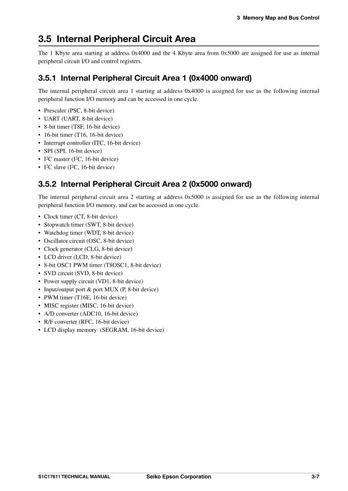
3 Memory Map and Bus Control
S1C17611 TECHNICAL MANUAL Seiko Epson Corporation 3-7
3.5 Internal Peripheral Circuit AreaThe 1 Kbyte area starting at address 0x4000 and the 4 Kbyte area from 0x5000 are assigned for use as internal peripheral circuit I/O and control registers.
3.5.1 Internal Peripheral Circuit Area 1 (0x4000 onward)
The internal peripheral circuit area 1 starting at address 0x4000 is assigned for use as the following internal peripheral function I/O memory and can be accessed in one cycle.
• Prescaler (PSC, 8-bit device)• UART (UART, 8-bit device)• 8-bit timer (T8F, 16-bit device)• 16-bit timer (T16, 16-bit device)• Interrupt controller (ITC, 16-bit device)• SPI (SPI, 16-bit device)• I2C master (I2C, 16-bit device)• I2C slave (I2C, 16-bit device)
3.5.2 Internal Peripheral Circuit Area 2 (0x5000 onward)
The internal peripheral circuit area 2 starting at address 0x5000 is assigned for use as the following internal peripheral function I/O memory, and can be accessed in one cycle.
• Clock timer (CT, 8-bit device)• Stopwatch timer (SWT, 8-bit device)• Watchdog timer (WDT, 8-bit device)• Oscillator circuit (OSC, 8-bit device)• Clock generator (CLG, 8-bit device)• LCD driver (LCD, 8-bit device)• 8-bit OSC1 PWM timer (T8OSC1, 8-bit device)• SVD circuit (SVD, 8-bit device)• Power supply circuit (VD1, 8-bit device)• Input/output port & port MUX (P, 8-bit device)• PWM timer (T16E, 16-bit device)• MISC register (MISC, 16-bit device)• A/D converter (ADC10, 16-bit device)• R/F converter (RFC, 16-bit device)• LCD display memory (SEGRAM, 16-bit device)
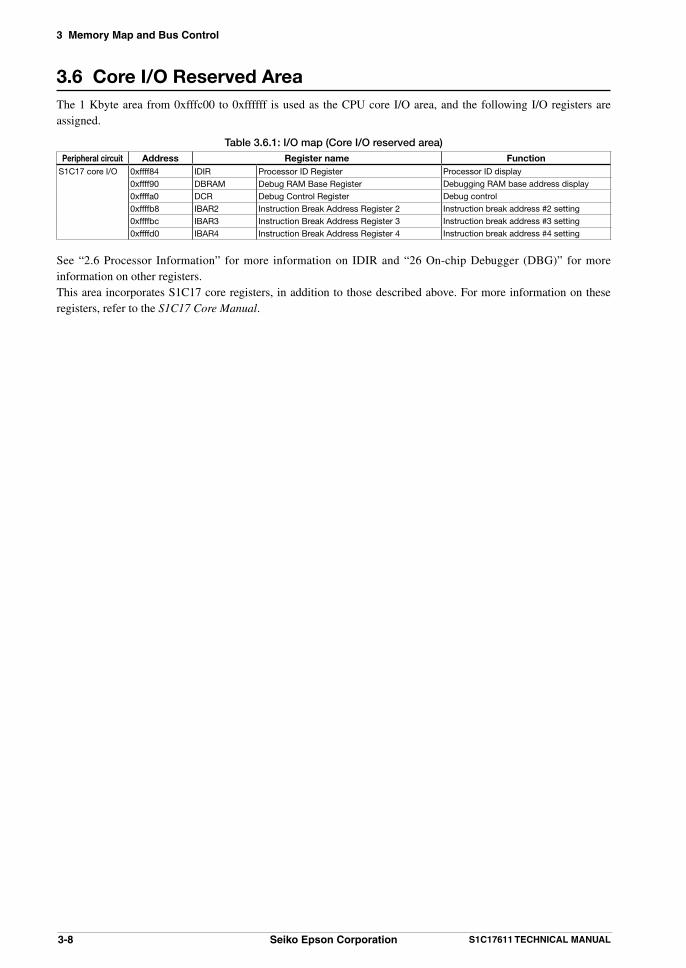
3 Memory Map and Bus Control
3-8 Seiko Epson Corporation S1C17611 TECHNICAL MANUAL
3.6 Core I/O Reserved AreaThe 1 Kbyte area from 0xfffc00 to 0xffffff is used as the CPU core I/O area, and the following I/O registers are assigned.
Table 3.6.1: I/O map (Core I/O reserved area)Peripheral circuit Address Register name Function
S1C17 core I/O 0xffff84 IDIR Processor ID Register Processor ID display
0xffff90 DBRAM Debug RAM Base Register Debugging RAM base address display
0xffffa0 DCR Debug Control Register Debug control
0xffffb8 IBAR2 Instruction Break Address Register 2 Instruction break address #2 setting
0xffffbc IBAR3 Instruction Break Address Register 3 Instruction break address #3 setting
0xffffd0 IBAR4 Instruction Break Address Register 4 Instruction break address #4 setting
See “2.6 Processor Information” for more information on IDIR and “26 On-chip Debugger (DBG)” for more information on other registers.This area incorporates S1C17 core registers, in addition to those described above. For more information on these registers, refer to the S1C17 Core Manual.

4 Power Supply Voltage
S1C17611 TECHNICAL MANUAL Seiko Epson Corporation 4-1
4 Power Supply Voltage
4.1 Power Supply VoltageThe S1C17611 operation power supply voltages are given below.
Normal operation: 1.8 V to 3.6 VFlash memory programming: 2.7 V to 3.6 V
Supply voltages within the respective ranges to VDD pin with the VSS pin as GND.
The S1C17611 QFP12-48 pin package has one VDD pin and one VSS pin. All must be connected to the + power supply and GND rather than left open.
Power supply voltage for Analog Circuit (AVDD) Built-in analog circuit (A/D Converter) sets power supply voltage pins (AVDD) for separate analog circuit,
having a power supply voltage pin as mentioned above in such a way that the influence of digital circuit is avoided.
Power supply voltage in the analog circuit is passed to the AVDD pins and VSS pins is considered as GND level. Supply power voltage level similar to VDD in AVDD.
AVDD = VDD, VSS = GND
Note: VDD power supply voltage should be supplied to the AVDD pins also when analog circuit is not in used.
It is required to take precaution regarding the noise in the analog power supply voltage line while generating the power supply voltage and board pattern, since affects A/D conversion accuracy.

4 Power Supply Voltage
4-2 Seiko Epson Corporation S1C17611 TECHNICAL MANUAL
4.2 Internal Power Supply CircuitThe S1C17611 includes a power supply circuit, as shown in Figure 4.2.1, which generates all the voltages required for internal circuits within the IC. Broadly speaking, the power supply circuit is divided into two sections.
Table 4.2.1: Power supply circuit
Circuit Power supply circuit Output voltageOscillator circuit, internal circuit Internal constant-voltage circuit VD1
LCD driver LCD constant-voltage circuit VC1 to VC3
VD1
VDD
VC1 to VC3
External power supply
Oscillator circuit
Internal constant-voltage circuit
VD1MD
Internal circuit
OSC1, OSC2
OSC3, OSC4
VDD
VD1
VC1
VC2
VC3
CACB
VSS
LCD driverCOM0 to COM7
SEG0 to SEG7
LHVLD
VCSEL
HVLD
LCD constant-voltage circuit
Figure 4.2.1: Power supply circuit configuration
Note: Never use the output from pins VD1 and VC1 to VC3 to drive external circuits.
Internal constant-voltage circuit The internal constant-voltage circuit generates voltage VD1 to operate internal logic and oscillator circuits. The
voltage of VD1 can be switched via the program and is set to 1.8 V for normal operations and 2.5 V for flash memory programming.
LCD constant-voltage circuit The LCD constant-voltage circuit generates 1/3 bias voltages VC1, VC2, and VC3 for driving LCDs. In the S1C17611, these LCD drive voltages are fed to the internal LCD driver to drive the LCD panels
connected to the common/segment pins. Select VCSEL according to the power supply voltage VDD. As compared to the VC1 reference voltage, the VC2
reference voltage is lower in current consumption.
Table 4.2.2: Correspondence between Power supply voltage VDD and VCSEL
Power supply voltage VDD Setting value of VCSEL1.8 to 3.6V 02.5 to 3.6V 1
Note: Voltages VC1 to VC3 cannot be obtained correctly if VDD is used by setting 1 to VCSEL when 2.5 V or less.

4 Power Supply Voltage
S1C17611 TECHNICAL MANUAL Seiko Epson Corporation 4-3
4.3 Power Supply Circuit ControlThe various power supply circuits can be controlled via software to ensure that correct operating voltages within the chip are generated to suit the power supply voltage and operating mode and to minimize consumption current.
Operating mode switching The S1C17611 features two operating modes: 1. Normal operating mode
Normal operating mode for running application programs. VDD = 1.8 V to 3.6 V, internal operating voltage VD1 = 1.8 V
2. Flash deletion/programming mode Operating mode for deleting and writing program/data to flash memory. VDD = 2.7 V to 3.6 V, internal operating voltage VD1 = 2.5 V
The voltage VD1 must be switched as described to suit the operating mode above. This is done using VD1MD (D0/VD1_CTL register). VD1MD is normally used with the default setting 0 (VD1 = 1.8 V). VD1MD is set to 1 for flash memory deletion/programming.
* VD1MD: Flash Erase/Program Mode Bit in the VD1 Control (VD1_CTL) Register (D0/0x5120)
Note: An interval of 5 ms (max.) is required for the internal operating voltage to stabilize after switching the operating mode. Start flash memory programming only after this stabilization time has elapsed.
LCD power supply control LCD drive voltages VC1 to VC3 are fed to the LCD driver if DSPC[1:0] (D[1:0]/LCD_DCTL register) is set to a
value other than 0x0 (display off).
* DSPC[1:0]: LCD Display Control Bits in the LCD Display Control (LCD_DCTL) Register (D[1:0]/0x50a0)
If the internal LCD driver is not used, turn off LCD constant-voltage circuit to minimize current consumption. DSPC[1:0] should all be 0 (default).
Power supply control bit settings list Table 4.3.1 lists the power supply control bit settings for different conditions.
Table 4.3.1: Power supply control bit settings listCondition Control bit
Operating mode VDD LCD driver VD1MD VCSEL DSPC[1:0]Normal operation 1.8 to 2.5V Used 0 0 Other than 0x0
2.5 to 3.6V Used 0 1 Other than 0x01.8 to 3.6V Not used 0 0 0x0
Flash deletion/programming
1.8 to 2.7V – (Not to be used)2.7 to 3.6V Used 1 1 Other than 0x02.7 to 3.6V Not used 1 0 0x0
For specific information on DSPC[1:0] settings, refer to “0x50a0: LCD Display Control Register (LCD_DCTL)” in section 22.8.

4 Power Supply Voltage
4-4 Seiko Epson Corporation S1C17611 TECHNICAL MANUAL
4.4 Heavy Load Protection FunctionThe internal constant-voltage and LCD constant-voltage circuits include heavy load protection functions that can be set via software to ensure stable operations and LCD display, even when the power supply voltage fluctuates due to external loads.The internal constant-voltage circuit is switched to Heavy Load Protection mode by writing 1 to HVLD (D5/VD1_CTL register), stabilizing VD1 output. If the unstable operation occurs by programming operations as the below, Use the heavy load protection function.
• The case of driving the high current consumption such as diode, buzzer and so on by the port outputs; set the heavy load protection function to enable during driving the diode or buzzer.
• The case of having the high current consumption difference between high clock and low clock using by system clock; set the heavy load protection function to enable during several ten micro seconds from in front of the change to end of the change.
• The case of having the high current consumption difference between HALT/SLEEP mode and those releases, and of changing frequently them; set the heavy load protection function to enable during repeating their process.
Note: Release the heavy load protection function after the unstable operations finished. In addition, If the unstable operations occur frequently, set the heavy load protection function to enable during these operations.
* HVLD: VD1 Heavy Load Protection Mode Bit in the VD1 Control (VD1_CTL) Register (D5/0x5120)
The LCD constant-voltage circuit is switched to Heavy Load Protection mode by writing 1 to LHVLD (D4/LCD_VREG register), stabilizing the VC1 to VC3 output. Make this setting if you observe brightness fluctuations on the LCD display.
* LHVLD: LCD Heavy Load Protection Mode Bit in the LCD Voltage Regulator Control (LCD_VREG) Register (D4/0x50a3)
Note: Current consumption will be higher in Heavy Load Protection mode than normal operations. Avoid setting Heavy Load Protection via software unless necessary.
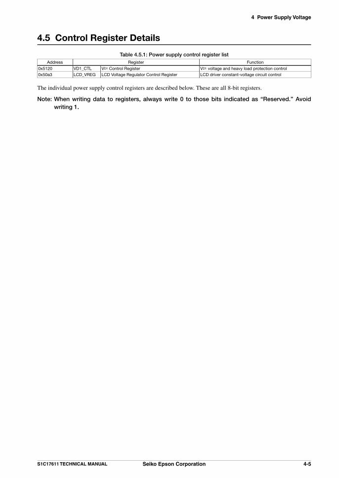
4 Power Supply Voltage
S1C17611 TECHNICAL MANUAL Seiko Epson Corporation 4-5
4.5 Control Register Details
Table 4.5.1: Power supply control register listAddress Register Function
0x5120 VD1_CTL VD1 Control Register VD1 voltage and heavy load protection control0x50a3 LCD_VREG LCD Voltage Regulator Control Register LCD driver constant-voltage circuit control
The individual power supply control registers are described below. These are all 8-bit registers.
Note: When writing data to registers, always write 0 to those bits indicated as “Reserved.” Avoid writing 1.

4 Power Supply Voltage
4-6 Seiko Epson Corporation S1C17611 TECHNICAL MANUAL
0x5120: VD1 Control Register (VD1_CTL)Register name Address Bit Name Function Setting Init. R/W Remarks
VD1 Control Register(VD1_CTL)
0x5120(8 bits)
D7–6 – reserved – – – 0 when being read.D5 HVLD VD1 heavy load protection mode 1 On 0 Off 0 R/WD4 – reserved – 0 R/W
D3–1 – reserved – – – 0 when being read.D0 VD1MD Flash erase/program mode 1 Flash (2.5 V) 0 Norm.(1.8 V) 0 R/W
D[7:6] Reserved
D5 HVLD: VD1 Heavy Load Protection Mode Bit Sets the internal constant-voltage circuit to Heavy Load Protection mode. 1 (R/W): Heavy load protection on 0 (R/W): Heavy load protection off (default)
The internal constant-voltage circuit is switched to Heavy Load Protection mode by writing 1 to HVLD, stabilizing the VD1 output. Make this setting before driving heavy loads such as lamps and buzzers using the port output. Since it increases current consumption, avoid setting Heavy Load Protection mode unless necessary.
D[4:1] Reserved
D0 VD1MD: Flash Erase/Program Mode Bit Selects the internal operating voltage VD1 value (operating mode). 1 (R/W): VD1 = 2.5 V, Flash deletion/programming mode 0 (R/W): VD1 = 1.8 V, Normal operating mode (default)
VD1MD is normally used with the default setting of 0 (VD1 = 1.8 V). Set VD1MD to 1 for flash memory deletion/programming.
Note: An interval of 5 ms (max) is required for the internal operating voltage to stabilize after switching the operating mode. Start flash memory programming after this stabilization time has elapsed.

4 Power Supply Voltage
S1C17611 TECHNICAL MANUAL Seiko Epson Corporation 4-7
0x50a3: LCD Voltage Regulator Control Register (LCD_VREG)Register name Address Bit Name Function Setting Init. R/W Remarks
LCD Voltage RegulatorControl Register(LCD_VREG)
0x50a3(8 bits)
D7–5 – reserved – – – 0 when being read.D4 LHVLD LCD heavy load protection mode 1 On 0 Off 0 R/W
D3–1 – reserved – – – 0 when being read.D0 VCSEL Power source select for LCD
voltage regulator1 VC = 2V 0 VC = 1V 0 R/W
D[7:5] Reserved
D4 LHVLD: LCD Heavy Load Protection Mode Bit Sets the LCD constant-voltage circuit to Heavy Load Protection mode. 1 (R/W): Heavy load protection on 0 (R/W): Heavy load protection off (default)
The LCD constant-voltage circuit is switched to Heavy Load Protection mode by writing 1 to LHVLD, stabilizing the VC1 to VC3 output. Make this setting if you observe brightness fluctuations on the LCD display.
Since it increases current consumption, avoid setting Heavy Load Protection mode unless necessary.
D[3:1] Reserved
D0 VCSEL: Power Source Select for LCD Voltage Regulator Set value according to the Power Supply Voltage VDD. 1 (R/W): Power supply voltage VDD 2.5 to 3.6 V 0 (R/W): Power supply voltage VDD 1.8 to 2.5 V

4 Power Supply Voltage
4-8 Seiko Epson Corporation S1C17611 TECHNICAL MANUAL
4.6 Precautions• Never use the output from pins VD1 and VC1 to VC3 to drive external circuits.
• The correct VC1 to VC3 voltages will not be obtained if you use VDD by secting 1 to VCSEL when 2.5 V or less.
• An interval of 5 ms (max.) is required for the internal operating voltage to stabilize after switching the operating mode to Flash deletion/programming mode. Start flash memory programming after this stabilization time has elapsed.
• Current consumption will be higher in Heavy Load Protection mode than for normal operation. Avoid setting Heavy Load Protection mode via software unless necessary.

5 Initial Reset
S1C17611 TECHNICAL MANUAL Seiko Epson Corporation 5-1
5 Initial Reset
5.1 Initial Reset FactorsShown below are the three different initial reset factors for initializing S1C17611 internal circuits.
(1) External initial reset via #RESET pin(2) External initial reset via P0 port (pins P02 to P05) key entry (set by software)(3) Internal initial reset via watchdog timer (set by software)
Figure 5.1.1 illustrates the initial reset circuit configuration.
Digital noise filter
Key reset control circuit
Chattering filter circuit
InternalresetS
R
Q
#RESET
P02P03P04P05
P0KRST
WDTMD
Watchdog timer
Oscillation stabilizationstandby circuit
VDD
Figure 5.1.1: Initial reset circuit configuration
The CPU and peripheral circuits are initialized by initial reset factors. The CPU begins reset processing once the factors are canceled.This causes the reset vector to be read from the start of the vector table, and the program (initialization routine) starting at that address to be executed.
5.1.1 #RESET pin
Initial resetting is possible by inputting external Low level to the #RESET pin.To initialize the S1C17611 reliably, the #RESET pin must be maintained at Low level for at least the specified duration after the power supply voltage rises. (Refer to “28.4 Input/Output Pin Characteristics”)Initial resetting is canceled if the #RESET input changes from Low to High, and the CPU begins reset interrupt processing.The #RESET pin incorporates a pull-up resistance.

5 Initial Reset
5-2 Seiko Epson Corporation S1C17611 TECHNICAL MANUAL
5.1.2 P0 Port Key-Entry Reset
Initial resetting is possible by inputting external Low level simultaneously to the ports (P02 to P05) selected by software. The ports can be selected by P0KRST[1:0] (D[1:0]/P0_KRST register).
* P0KRST[1:0]: P0 Port Key-Entry Reset Configuration Bits in the P0 Port Key-Entry Reset Configuration (P0_KRST) Register (D[1:0]/0x5209)
Table 5.1.2.1: P0 port key-entry reset settings
P0KRST[1:0] Port used0x3 P02, P03, P04, P050x2 P02, P03, P040x1 P02, P030x0 Not used
For example, initial reset is applied when input to the four ports P02 to P05 is Low level simultaneously if P0KRST[1:0] is set to 0x3.
Note: • Make sure the specified ports are not simultaneously switched to Low during normal operations when using the P0 port key-entry reset function.
• The P0 port key-entry reset function is enabled by software and cannot be used to perform a reset at power-on.
5.1.3 Reset by Watchdog Timer
The S1C17611 incorporates a watchdog timer to detect runaway CPU. If the watchdog timer is not reset by software every 4 seconds (with this failure indicating a runaway CPU), the timer overflows, generating an NMI or reset. A reset is generated by writing “1” to WDTMD (D1/WDT_ST register). (NMI is generated if WDTMD is 0.)
*WDTMD: NMI/Reset Mode Select Bit in the Watchdog Timer Status (WDT_ST) Register (D1/0x5041)
For detailed information on the watchdog timer, refer to “17 Watchdog Timer (WDT).”
Note: • When using the reset function with the watchdog timer, to prevent accidental resetting, take care to program so that the watchdog timer is reset every four seconds.
• The watchdog timer reset function is enabled by software and cannot be used to perform a reset at power-on.

5 Initial Reset
S1C17611 TECHNICAL MANUAL Seiko Epson Corporation 5-3
5.2 Initial Reset SequenceCPU startup waits for the oscillation stabilization standby time to expire after resetting is cancelled via the #RESET pin at power-on. Figure 5.2.1 illustrates the sequence of operations after canceling the initial reset. The CPU starts up in sync with the IOSC (internal CR oscillation circuit) clock after the reset is canceled.
*fIOSC: IOSC clock frequency
Note: The oscillation stabilization standby time does not include the oscillation start time. The time may be longer than that shown between power-on or SLEEP cancellation and instruction execution.
Boot vector
Oscillationstabilizationstandby time
Boot operation start
IOSC clock
#RESET
Internal reset
Internal data request
Internal data address
Internal resetcancellation
Resetcancellation
Figure 5.2.1: Sequence of operations after initial reset cancellation

5 Initial Reset
5-4 Seiko Epson Corporation S1C17611 TECHNICAL MANUAL
5.3 Initial Settings at Initial ResettingThe CPU internal register is initialized by initial resetting, as shown below.
R0 to R7: 0x0PSR: 0x0 (interrupt level = 0, interrupt prohibited)SP: 0x0PC: Reset vector at start of vector table is loaded by reset processing.
The internal RAM and display memory should be initialized via software, since they are not initialized by initial resetting.
The internal peripheral circuits are initialized in accordance with their particular specifications. They should be reset via software, if necessary. For detailed information on initial values after initial resetting, refer to the I/O register list in the Appendix or the respective peripheral circuit descriptions.

6 Interrupt Controller (ITC)
S1C17611 TECHNICAL MANUAL Seiko Epson Corporation 6-1
6 Interrupt Controller (ITC)
6.1 ITC ConfigurationThe ITC enables the interrupt level (priority) for determining the processing sequence when multiple maskable interrupts occur simultaneously to be set for each interrupt type separately. For details on the maskable interrupt types, refer to the vector table shown in the next page.Each interrupt type has the number of interrupt factors as shown in parentheses in the table mentioned above. Settings to permit or prohibit interrupt for different factors are set by the respective peripheral module registers.For specific information on interrupt factors and their control, refer to the peripheral module explanations.Figure 6.1.1 illustrates the interrupt system configuration.
S1C17 core Interrupt controller
Watchdog timer
Interrupt level
Interrupt control
Vector number
Peripheral module
Interrupt enable
Interrupt factor 1
Interrupt level
Vector number
Interrupt enable
Interrupt factor n
Peripheral module
Interrupt enable
Interrupt factor 1
Interrupt enable
Interrupt factor n
• •
• •
•
• •
•
• •
• •
• •
• •
Interrupt flag
Interrupt flag
Interrupt flag
Interrupt flag
Interrupt request
Interrupt request
NMI
Interrupt request
Debug signalReset signal
Interrupt level
Vector number
Figure 6.1.1: Interrupt system

6 Interrupt Controller (ITC)
6-2 Seiko Epson Corporation S1C17611 TECHNICAL MANUAL
6.2 Vector TableThe vector table contains the vectors (processing routine start addresses) for interrupt processing routines. When an interrupt occurs, the S1C17 core reads the vector corresponding to the interrupt and executes that processing routine. The base (top) address for the vector table can be set using the MISC_TTBRL and MISC_TTBRH registers (0x5328 and 0x532a) (See “2.4 Vector Table”). “TTBR” in Table 6.2.1 indicates the values set for these registers. The MISC_TTBRL and MISC_TTBRH registers are set to the 0x8000 address after initial resetting. Table 6.2.1 shows the S1C17611 vector table.
Table 6.2.1: Vector tableVector No./ Soft-
ware interrupt No.Vector
addressHardware interrupt name Hardware interrupt factor Priority Mask
0 (0x00) TTBR + 0x00 Reset • Low input to #RESET pin• Watchdog timer overflow *2
1 impos-sible
1 (0x01) TTBR + 0x04 Irregular address interrupt Memory access instruction 2– (0xfffc00) Debug interrupt brk instruction etc. 3
2 (0x02) TTBR + 0x08 NMI Watchdog timer overflow *2 4 3 (0x03) TTBR + 0x0c C Compiler (reserved) Use emulation library of C compiler – 4 (0x04) TTBR + 0x10 P0 port interrupt P00 to P07 port input High *1 Possible
5 (0x05) TTBR + 0x14 P1 port interrupt P10 to P17 port input 6 (0x06) TTBR + 0x18 Stopwatch timer interrupt • Timer 100 Hz signal
• Timer 10 Hz signal• Timer 1 Hz signal
7 (0x07) TTBR + 0x1c Clock timer interrupt • Timer 32 Hz signal• Timer 8 Hz signal• Timer 2 Hz signal• Timer 1 Hz signal
8 (0x08) TTBR + 0x20 8-bit OSC1 timer interrupt Compare match 9 (0x09) TTBR + 0x24 SVD interrupt Power supply voltage drop detection10 (0x0a) TTBR + 0x28 LCD interrupt Frame signal11 (0x0b) TTBR + 0x2c PWM timer Ch.0 interrupt • Compare A
• Compare B12 (0x0c) TTBR + 0x30 8-bit timer interrupt Timer underflow13 (0x0d) TTBR + 0x34 16-bit timer Ch.0 interrupt Timer underflow14 (0x0e) TTBR + 0x38 16-bit timer Ch.1 interrupt Timer underflow15 (0x0f) TTBR + 0x3c 16-bit timer Ch.2 interrupt Timer underflow16 (0x10) TTBR + 0x40 UART interrupt • Transmit buffer empty
• Receive buffer full• Receive error
17 (0x11) TTBR + 0x44 I2C (slave) interrupt • I2C (slave) transmit buffer empty• I2C (slave) receive buffer full• I2C (slave) bus status change
18 (0x12) TTBR + 0x48 SPI interrupt • Transmit buffer empty (only Master mode)• Receive buffer full
19 (0x13) TTBR + 0x4c I2C (master) interrupt • Transmit buffer empty• Receive buffer full
20 (0x14) TTBR + 0x50 PWM timer Ch.1 interrupt • Compare A• Compare B
21 (0x15) TTBR + 0x54 reserved –22 (0x16) TTBR + 0x58 A/D converter interrupt • Conversion finish
• Conversion result overwrite23 (0x17) TTBR + 0x5c R/F converter interrupt • Standard oscillation finish
• Sensor A oscillation finish• Sensor B oscillation finish• Timebase counter overflow• Measurement counter overflow
24 (0x18) TTBR + 0x60 reserved –: : : :
31 (0x1f) TTBR + 0x7c reserved – Low *1
*1: When same interrupt level is set*2: Watchdog timer interrupt selects reset or NMI using software.
Vector numbers 4 to 20, 22 to 23 are assigned maskable interrupts supported by the S1C17611.

6 Interrupt Controller (ITC)
S1C17611 TECHNICAL MANUAL Seiko Epson Corporation 6-3
6.3 Maskable Interrupt Control
6.3.1 Peripheral Module Interrupt Control Bit
The peripheral module causing the interrupt includes interrupt enable bits and interrupt flags for each interrupt cause. Setting the interrupt enable bit to 1 (interrupt permitted) sets the interrupt flag to 1, depending on the cause of the interrupt. The flag state is sent to the ITC as an interrupt request signal, generating an interrupt request to the S1C17 core. The corresponding interrupt enable bits should be set to 0 for those causes for which interrupts are not desired. In this case, the interrupt flag will not be set to 1, even if the interrupt cause occurs, and the interrupt request signal will not be activated to the ITC.Interrupt flags set to 1 must be reset within the interrupt processing routine after the interrupt has occurred. The ITC will generate the same interrupt again once the interrupt processing routine has been ended by the reti instruction with the interrupt flag still set to 1, since it detects interrupt requests using the signal level.For specific information on interrupt causes, interrupt flags, and interrupt enable bits, refer to the individual peripheral module descriptions.
6.3.2 ITC Interrupt Request Processing
On receiving an interrupt signal from a peripheral module, the ITC sends interrupt request, interrupt level, and vector number signals to the S1C17 core.Vector numbers are determined by the ITC internal hardware for each interrupt cause, as shown in Table 6.2.1.The interrupt level is a value used by the S1C17 core to compare with the IL bit (PSR). This interrupt level is used in the S1C17 core to prohibit subsequently occurring interrupts with the same or lower level. (See section 6.3.3.)The default ITC settings are level 0 for all maskable interrupts. Interrupt requests are not accepted by the S1C17 core if the level is 0.The ITC includes control bits for selecting the interrupt level, and these can be set to between 0 (low) and 7 (high) interrupt levels for each interrupt type.
Table 6.3.2.1: Interrupt level setting bits
Hardware interrupt Interrupt level setting bit Register addressP0 port interrupt ILV0[2:0] (D[2:0]/ITC_LV0 register) 0x4306P1 port interrupt ILV1[2:0] (D[10:8]/ITC_LV0 register) 0x4306Stopwatch timer interrupt ILV2[2:0] (D[2:0]/ITC_LV1 register) 0x4308Clock timer interrupt ILV3[2:0] (D[10:8]/ITC_LV1 register) 0x43088-bit OSC1 timer interrupt ILV4[2:0] (D[2:0]/ITC_LV2 register) 0x430aSVD interrupt ILV5[2:0] (D[10:8]/ITC_LV2 register) 0x430aLCD interrupt ILV6[2:0] (D[2:0]/ITC_LV3 register) 0x430cPWM timer Ch.0 interrupt ILV7[2:0] (D[10:8]/ITC_LV3 register) 0x430c8-bit timer interrupt ILV8[2:0] (D[2:0]/ITC_LV4 register) 0x430e16-bit timer Ch.0 interrupt ILV9[2:0] (D[10:8]/ITC_LV4 register) 0x430e16-bit timer Ch.1 interrupt ILV10[2:0] (D[2:0]/ITC_LV5 register) 0x431016-bit timer Ch.2 interrupt ILV11[2:0] (D[10:8]/ITC_LV5 register) 0x4310UART interrupt ILV12[2:0] (D[2:0]/ITC_LV6 register) 0x4312I2C (slave) interrupt ILV13[2:0] (D[10:8]/ITC_LV6 register) 0x4312SPI interrupt ILV14[2:0] (D[2:0]/ITC_LV7 register) 0x4314I2C (master) interrupt ILV15[2:0] (D[10:8]/ITC_LV7 register) 0x4314PWM timer Ch.1 interrupt ILV16[2:0] (D[2:0]/ITC_LV8 register) 0x4316reserved ILV17[2:0] (D[10:8]/ITC_LV8 register) 0x4316A/D Conveter interrupt ILV18[2:0] (D[2:0]/ITC_LV9 register) 0x4318R/F Conveter interrupt ILV19[2:0] (D[10:8]/ITC_LV9 register) 0x4318

6 Interrupt Controller (ITC)
6-4 Seiko Epson Corporation S1C17611 TECHNICAL MANUAL
If interrupt requests are input to the ITC simultaneously from multiple peripheral modules, the ITC outputs the interrupt request with the highest priority to the S1C17 core in accordance with the following conditions.1. Interrupts with the highest interrupt level take precedence.2. If multiple interrupt requests are input with the same interrupt level, the interrupt with the lowest vector number
takes precedence.
The other interrupts occurring at the same time are held until all have been accepted by the S1C17 core, in descending order of priority.If an interrupt cause with higher priority occurs while the ITC is outputting an interrupt request signal to the S1C17 core (before being accepted by the S1C17 core), the ITC alters the vector number and interrupt level signal to the setting information on the more recent interrupt. The previously occurring interrupt is held.No interrupt is generated if the interrupt flag is reset via software within the peripheral module outputting an interrupt request held.
6.3.3 S1C17 Core Interrupt Processing
Maskable interrupts for the S1C17 core occur when all of the following conditions are met:
• Interrupts are permitted by the interrupt control bit inside the peripheral module.
• The PSR (S1C17 core internal processor status register) IE (interrupt enable) bit has been set to 1.
• The interrupt factor has a higher interrupt level set than that set for the PSR IL (interrupt level).
• No other interrupt factors having higher procedence (e.g., NMI) are present.
If an interrupt cause permitted inside the peripheral module occurs, the corresponding interrupt flag is set to 1, and this state is maintained until it is reset by the program. This means the interrupt cause is not cleared even if the conditions listed above are not met when the interrupt cause occurs. An interrupt occurs if the above conditions are met.If multiple maskable interrupt causes arise simultaneously, the interrupt cause with the highest interrupt level and lowest vector number becomes the subject of the interrupt request to the S1C17 core. Interrupts with lower levels are held until the above conditions are subsequently met.
The S1C17 core samples interrupt requests for each cycle. On accepting an interrupt request, the S1C17 core switches to interrupt processing when execution of the current instruction is complete.Interrupt processing involves the following steps:
(1) The PSR and current program counter (PC) value is moved to the stack.(2) The PSR IE bit is reset to 0 (preventing subsequent maskable interrupts).(3) The PSR IL is set to the received interrupt level. (The NMI does not affect interrupt levels.)(4) The vector for the interrupt factor occurring is loaded to the PC to execute the interrupt processing routine.
When an interrupt is received, (2) prevents subsequent maskable interrupts. Setting the IE bit to 1 within the interrupt processing routine allows handling of multiple interrupts. In this case, IL is changed by (3), and only interrupts with higher levels than those already being processed will be accepted.Ending interrupt processing routines using a reti instruction returns the PSR to the state before the interrupt. The program resumes processing following the instruction being executed at the time the interrupt occurred via the next branch.
6 Interrupt Controller (ITC)
S1C17611 TECHNICAL MANUAL Seiko Epson Corporation 6-5
6.4 NMIThe S1C17611 can generate NMIs (non-maskable interrupts) using the watchdog timer. The vector number for NMIs is 2, and the vector address is set in the vector table initial address + 8 bytes. These interrupts take precedence over other interrupt factors and are accepted unconditionally by the S1C17 core.
For detailed information on generating NMIs, refer to “17 Watchdog Timer (WDT).”

6 Interrupt Controller (ITC)
6-6 Seiko Epson Corporation S1C17611 TECHNICAL MANUAL
6.5 Software InterruptsInterrupts can be generated via software with S1C17 core int imm5 or intl imm5 and imm3 instructions. The vector table vector number (0 to 31) is specified by the operand immediate imm5. With the intl instruction, imm3 can be used to specify an interrupt level (0 to 7) for the PSR IL fields.Details of the processor interrupt processing are the same as for when an interrupt generated by hardware occurs.

6 Interrupt Controller (ITC)
S1C17611 TECHNICAL MANUAL Seiko Epson Corporation 6-7
6.6 HALT and SLEEP Mode CancellationHALT or SLEEP mode is released by the following signals, and the CPU starts up.• Interrupt requests from the ITC to the CPU.• The NMI from the watchdog timer. • Debug interrupts• Reset
Note: When HALT or SLEEP mode is released by an interrupt request from the ITC to the CPU, the process branches to an interrupt routine immediately after the release if the CPU can permit interrupts. Otherwise, the process executes an instruction following the halt or slp instruction.
The ITC interrupt level setting cannot mask the release of HALT or SLEEP mode.
For details, refer to “C.1 Clock Control Power Saving” in Appendix C.
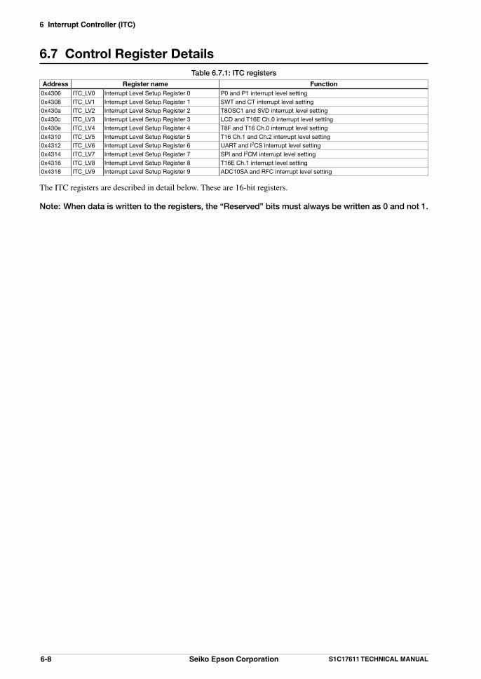
6 Interrupt Controller (ITC)
6-8 Seiko Epson Corporation S1C17611 TECHNICAL MANUAL
6.7 Control Register DetailsTable 6.7.1: ITC registers
Address Register name Function0x4306 ITC_LV0 Interrupt Level Setup Register 0 P0 and P1 interrupt level setting0x4308 ITC_LV1 Interrupt Level Setup Register 1 SWT and CT interrupt level setting0x430a ITC_LV2 Interrupt Level Setup Register 2 T8OSC1 and SVD interrupt level setting0x430c ITC_LV3 Interrupt Level Setup Register 3 LCD and T16E Ch.0 interrupt level setting0x430e ITC_LV4 Interrupt Level Setup Register 4 T8F and T16 Ch.0 interrupt level setting0x4310 ITC_LV5 Interrupt Level Setup Register 5 T16 Ch.1 and Ch.2 interrupt level setting0x4312 ITC_LV6 Interrupt Level Setup Register 6 UART and I2CS interrupt level setting0x4314 ITC_LV7 Interrupt Level Setup Register 7 SPI and I2CM interrupt level setting0x4316 ITC_LV8 Interrupt Level Setup Register 8 T16E Ch.1 interrupt level setting0x4318 ITC_LV9 Interrupt Level Setup Register 9 ADC10SA and RFC interrupt level setting
The ITC registers are described in detail below. These are 16-bit registers.
Note: When data is written to the registers, the “Reserved” bits must always be written as 0 and not 1.

6 Interrupt Controller (ITC)
S1C17611 TECHNICAL MANUAL Seiko Epson Corporation 6-9
0x4306: Interrupt Level Setup Register 0 (ITC_LV0)Register name Address Bit Name Function Setting Init. R/W Remarks
Interrupt Level Setup Register 0(ITC_LV0)
0x4306(16 bits)
D15–11 – reserved – – – 0 when being read.D10–8 ILV1[2:0] P1 interrupt level 0 to 7 0x0 R/WD7–3 – reserved – – – 0 when being read.D2–0 ILV0[2:0] P0 interrupt level 0 to 7 0x0 R/W
D[15:11] Reserved
D[10:8] ILV1[2:0]: P1 Port Interrupt Level Bits Set the P1 port interrupt level (0 to 7). (Default: 0) The S1C17 core does not accept interrupts with levels set lower than the PSR IL value. The ITC uses the interrupt level when multiple interrupt factors occur simultaneously. If multiple interrupts occur at the same time permitted by the interrupt enable bit, the ITC sends the
interrupt request with the highest level set by the ITC_LVx registers (0x4306 to 0x4318) to the S1C17 core.
If multiple interrupt factors with the same interrupt level occur simultaneously, the interrupt with the lowest vector number is processed first.
The other interrupts are held until all have been accepted by the S1C17 core in descending order of priority.
If an interrupt factor of higher priority occurs while the ITC outputs an interrupt request signal to the S1C17 core (before acceptance by the S1C17 core), the ITC alters the vector number and interrupt level signal to the setting details of the most recent interrupt. The immediately preceding interrupt is held.
D[7:3] Reserved
D[2:0] ILV0[2:0]: P0 Port Interrupt Level Bits Set the P0 port interrupt level (0 to 7). (Default: 0) Refer to the ILV1[2:0] (D[10:8]) description.

6 Interrupt Controller (ITC)
6-10 Seiko Epson Corporation S1C17611 TECHNICAL MANUAL
0x4308: Interrupt Level Setup Register 1 (ITC_LV1)Register name Address Bit Name Function Setting Init. R/W Remarks
Interrupt Level Setup Register 1(ITC_LV1)
0x4308(16 bits)
D15–11 – reserved – – – 0 when being read.D10–8 ILV3[2:0] CT interrupt level 0 to 7 0x0 R/WD7–3 – reserved – – – 0 when being read.D2–0 ILV2[2:0] SWT interrupt level 0 to 7 0x0 R/W
D[15:11] Reserved
D[10:8] ILV3[2:0]: Clock Timer Interrupt Level Bits Set the clock timer interrupt level (0 to 7). (Default: 0) Refer to the ITC_LV0 register (0x4306) ILV1[2:0] (D[10:8]) description.
D[7:3] Reserved
D[2:0] ILV2[2:0]: Stopwatch Timer Interrupt Level Bits Set the stopwatch timer interrupt level (0 to 7). (Default: 0) Refer to the ITC_LV0 register (0x4306) ILV1[2:0] (D[10:8]) description.

6 Interrupt Controller (ITC)
S1C17611 TECHNICAL MANUAL Seiko Epson Corporation 6-11
0x430a: Interrupt Level Setup Register 2 (ITC_LV2)Register name Address Bit Name Function Setting Init. R/W Remarks
Interrupt Level Setup Register 2(ITC_LV2)
0x430a(16 bits)
D15–11 – reserved – – – 0 when being read.D10–8 ILV5[2:0] SVD interrupt level 0 to 7 0x0 R/WD7–3 – reserved – – – 0 when being read.D2–0 ILV4[2:0] T8OSC1 interrupt level 0 to 7 0x0 R/W
D[15:11] Reserved
D[10:8] ILV5[2:0]: SVD Interrupt Level Bits Set the SVD interrupt level (0 to 7). (Default: 0) Refer to the discussion of ITC_LV0 register (0x4306) ILV1[2:0] (D[10:8]).
D[7:3] Reserved
D[2:0] ILV4[2:0]: 8-bit OSC1 Timer Interrupt Level Bits Set the 8-bit OSC1 timer interrupt level (0 to 7). (Default: 0) Refer to the ITC_LV0 register (0x4306) ILV1[2:0] (D[10:8]) description.

6 Interrupt Controller (ITC)
6-12 Seiko Epson Corporation S1C17611 TECHNICAL MANUAL
0x430c: Interrupt Level Setup Register 3 (ITC_LV3)Register name Address Bit Name Function Setting Init. R/W Remarks
Interrupt Level Setup Register 3(ITC_LV3)
0x430c(16 bits)
D15–11 – reserved – – – 0 when being read.D10–8 ILV7[2:0] T16E Ch.0 interrupt level 0 to 7 0x0 R/WD7–3 – reserved – – – 0 when being read.D2–0 ILV6[2:0] LCD interrupt level 0 to 7 0x0 R/W
D[15:11] Reserved
D[10:8] ILV7[2:0]: PWM & Capture Timer Ch.0 Interrupt Level Bits Set the PWM timer interrupt level (0 to 7). (Default: 0) Refer to the ITC_LV0 register (0x4306) ILV1[2:0] (D[10:8]) description.
D[7:3] Reserved
D[2:0] ILV6[2:0]: LCD Interrupt Level Bits Set the LCD interrupt level (0 to 7). (Default: 0) Refer to the discussion of ITC_LV0 register (0x4306) ILV1[2:0] (D[10:8]).

6 Interrupt Controller (ITC)
S1C17611 TECHNICAL MANUAL Seiko Epson Corporation 6-13
0x430e: Interrupt Level Setup Register 4 (ITC_LV4)Register name Address Bit Name Function Setting Init. R/W Remarks
Interrupt Level Setup Register 4(ITC_LV4)
0x430e(16 bits)
D15–11 – reserved – – – 0 when being read.D10–8 ILV9[2:0] T16 Ch.0 interrupt level 0 to 7 0x0 R/WD7–3 – reserved – – – 0 when being read.D2–0 ILV8[2:0] T8F interrupt level 0 to 7 0x0 R/W
D[15:11] Reserved
D[10:8] ILV9[2:0]: 16-bit Timer Ch.0 Interrupt Level Bits Set the 16-bit timer Ch.0 interrupt level (0 to 7). (Default: 0) Refer to the discussion of ITC_LV0 register (0x4306) ILV1[2:0] (D[10:8]).
D[7:3] Reserved
D[2:0] ILV8[2:0]: 8-bit Timer Interrupt Level Bits Set the 8-bit timer interrupt level (0 to 7). (Default: 0) Refer to the ITC_LV0 register (0x4306) ILV1[2:0] (D[10:8]) description.
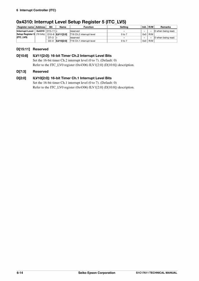
6 Interrupt Controller (ITC)
6-14 Seiko Epson Corporation S1C17611 TECHNICAL MANUAL
0x4310: Interrupt Level Setup Register 5 (ITC_LV5)Register name Address Bit Name Function Setting Init. R/W Remarks
Interrupt Level Setup Register 5(ITC_LV5)
0x4310(16 bits)
D15–11 – reserved – – – 0 when being read.D10–8 ILV11[2:0] T16 Ch.2 interrupt level 0 to 7 0x0 R/WD7–3 – reserved – – – 0 when being read.D2–0 ILV10[2:0] T16 Ch.1 interrupt level 0 to 7 0x0 R/W
D[15:11] Reserved
D[10:8] ILV11[2:0]: 16-bit Timer Ch.2 Interrupt Level Bits Set the 16-bit timer Ch.2 interrupt level (0 to 7). (Default: 0) Refer to the ITC_LV0 register (0x4306) ILV1[2:0] (D[10:8]) description.
D[7:3] Reserved
D[2:0] ILV10[2:0]: 16-bit Timer Ch.1 Interrupt Level Bits Set the 16-bit timer Ch.1 interrupt level (0 to 7). (Default: 0) Refer to the ITC_LV0 register (0x4306) ILV1[2:0] (D[10:8]) description.

6 Interrupt Controller (ITC)
S1C17611 TECHNICAL MANUAL Seiko Epson Corporation 6-15
0x4312: Interrupt Level Setup Register 6 (ITC_LV6)Register name Address Bit Name Function Setting Init. R/W Remarks
Interrupt Level Setup Register 6(ITC_LV6)
0x4312(16 bits)
D15–11 – reserved – – – 0 when being read.D10–8 ILV13[2:0] I2C slave interrupt level 0 to 7 0x0 R/WD7–3 – reserved – – – 0 when being read.D2–0 ILV12[2:0] UART interrupt level 0 to 7 0x0 R/W
D[15:11] Reserved
D[10:8] ILV13[2:0]: I2C slave Interrupt Level Bits Set the I2C (slave) interrupt level (0 to 7). (Default: 0) Refer to the ITC_LV0 register (0x4306) ILV1[2:0] (D[10:8]) description.
D[7:3] Reserved
D[2:0] ILV12[2:0]: UART Interrupt Level Bits Set the UART Ch.0 interrupt level (0 to 7). (Default: 0) Refer to the ITC_LV0 register (0x4306) ILV1[2:0] (D[10:8]) description.

6 Interrupt Controller (ITC)
6-16 Seiko Epson Corporation S1C17611 TECHNICAL MANUAL
0x4314: Interrupt Level Setup Register 7 (ITC_LV7)Register name Address Bit Name Function Setting Init. R/W Remarks
Interrupt Level Setup Register 7(ITC_LV7)
0x4314(16 bits)
D15–11 – reserved – – – 0 when being read.D10–8 ILV15[2:0] I2C master interrupt level 0 to 7 0x0 R/WD7–3 – reserved – – – 0 when being read.D2–0 ILV14[2:0] SPI interrupt level 0 to 7 0x0 R/W
D[15:11] Reserved
D[10:8] ILV15[2:0]: I2C master Interrupt Level Bits Set the I2C interrupt level (0 to 7). (Default: 0) Refer to the ITC_LV0 register (0x4306) ILV1[2:0] (D[10:8]) description.
D[7:3] Reserved
D[2:0] ILV14[2:0]: SPI Interrupt Level Bits Set the SPI interrupt level (0 to 7). (Default: 0) Refer to the ITC_LV0 register (0x4306) ILV1[2:0] (D[10:8]) description.

6 Interrupt Controller (ITC)
S1C17611 TECHNICAL MANUAL Seiko Epson Corporation 6-17
0x4316: Interrupt Level Setup Register 8 (ITC_LV8)Register name Address Bit Name Function Setting Init. R/W Remarks
Interrupt Level Setup Register 8(ITC_LV8)
0x4316(16 bits)
D15–3 – reserved – – – 0 when being read.D2–0 ILV16[2:0] T16E Ch.1 interrupt level 0 to 7 0x0 R/W
D[15:3] Reserved
D[2:0] ILV16[2:0]: PWM & Capture Timer Ch.1 Interrupt Level Bits Set the PWM Timer Ch.1 interrupt level (0 to 7). (Default: 0) Refer to the discussion of ITC_LV0 register (0x4306) ILV1[2:0] (D[10:8]).

6 Interrupt Controller (ITC)
6-18 Seiko Epson Corporation S1C17611 TECHNICAL MANUAL
0x4318: Interrupt Level Setup Register 9 (ITC_LV9)Register name Address Bit Name Function Setting Init. R/W Remarks
Interrupt Level Setup Register 9(ITC_LV9)
0x4318(16 bits)
D15–11 – reserved – – – 0 when being read.D10–8 ILV19[2:0] RFC interrupt level 0 to 7 0x0 R/WD7–3 – reserved – – – 0 when being read.D2–0 ILV18[2:0] ADC10SA interrupt level 0 to 7 0x0 R/W
D[15:11] Reserved
D[10:8] ILV19[2:0]: RFC Interrupt Level Bits Set the R/F converter interrupt level (0 to 7). (Default: 0) Refer to the discussion of ITC_LV0 register (0x4306) ILV1[2:0] (D[10:8]).
D[7:3] Reserved
D[2:0] ILV18[2:0]: ADC10SA Interrupt Level Bits Set the A/D converter interrupt level (0 to 7). (Default: 0) Refer to the discussion of ITC_LV0 register (0x4306) ILV1[2:0] (D[10:8]).

6 Interrupt Controller (ITC)
S1C17611 TECHNICAL MANUAL Seiko Epson Corporation 6-19
6.8 PrecautionsTo prevent the recurrence of interrupts due to the same interrupt factor, always reset the interrupt flag before permitting interrupts, resetting PSR, or executing the reti instruction.

6 Interrupt Controller (ITC)
6-20 Seiko Epson Corporation S1C17611 TECHNICAL MANUAL
This page intentionally left blank.

7 Oscillator Circuit (OSC)
S1C17611 TECHNICAL MANUAL Seiko Epson Corporation 7-1
7 Oscillator Circuit (OSC)
7.1 OSC Module ConfigurationThe S1C17611 contains three internal oscillator circuits (IOSC, OSC3, and OSC1). The IOSC and OSC3 oscillator circuits generate the main clock for high-speed operation of the S1C17 core and peripheral circuits. The OSC1 oscillator circuit generates a sub-clock for timer and low-power operations.The IOSC clock is selected as the system clock after initial resetting.Oscillator circuit on/off switching and system clock selection (between IOSC/OSC3 and OSC1) is controlled by software. External clock output is also possible.Figure 7.1.1 illustrates the clock system and OSC module configuration.
HSCLKCCLK
OSC1OSC3
IOSC
OSC1
FOUTHoutput circuit
OSC1oscillator circuit
Division circuit(1/1 to 1/4)
Wait circuit for wakeup
Clock gear(1/1 to 1/8)
Gate S1C17 core
BCLKInternal bus, RAM,Flash, LCD display RAM, Control regiser (LCD, RFC)
CLK_256Hz
Gate
FOUTH
FOUT1output circuitFOUT1
Noise filterRESET
OSC3oscillator circuit
OSC3OSC4
EXOSC3
OSC1
OSC2
HSCLK selection
wakeup
Wait circuit for wakeup
wakeup
HALT
HALT
Division circuit(1/1 to 1/16K)
Noise filterNMI
CT, SWT, WDT
T8OSC1
Division circuit
(1/128)
(1/1 to 1/32)
Gate
Gate
CLG
PSC
OSC
T16, T8F, UART, SPI, I2C (master), T16E, P, MISC, VD1, SVD, ADC, I2C (slave)
PCLKGate
T8F, T16, T16E, P, UART, SPI, I2C (master), ADC
LCLK
OSC1
HSCLK
HSCLK
HSCLK
SVD
OSC1
LCD
OSC1
RFC
Division circuit(1/512)
Division circuit(1/32 to 1/512)
Division circuit(1/1 to 1/8)
Gate
Gate
Gate
Clock sourceselection
Clock source selection
Clock source selection
Clock source selection
Systemclock
Gear selection
S1C17 core
S1C17 core
Division ratioselection
Division ratioselection
Division ratioselection
Division ratio selection On/off control
SLEEP, on/off control
On/off control
On/off control
On/off control
On/off control
IOSCoscillator circuit
SLEEP, on/off control
SLEEP, on/off control
On/off control
On/off control
On/off control
On/off control
On/off control
Clock source selection
Figure 7.1.1: OSC module configuration
To reduce power consumption, control the clock in conjunction with processing and use standby mode. For more information on reducing power consumption, refer to “Appendix C: Power Saving.”

7 Oscillator Circuit (OSC)
7-2 Seiko Epson Corporation S1C17611 TECHNICAL MANUAL
7.2 IOSC Oscillator CircuitThe IOSC oscillator initiates high-speed oscillation without external components. It initiates oscillation when power is turned on. The S1C17 Core and peripheral circuits operates with this oscillation clock after an initial reset.
fIOSCOscillation stabilization
wait circuitClock
generator
IOSCWT[1:0]IOSCEN
Figure 7.2.1: IOSC oscillator circuit
IOSC oscillation on/off The IOSC oscillator circuit stops oscillating if IOSCEN (D2/OSC_CTL register) is set to 0 and begins
oscillating if set to 1. The IOSC oscillator circuit stops oscillating even in SLEEP mode.
* IOSCEN: IOSC Enable Bit in the Oscillation Control (OSC_CTL) Register (D2/0x5061)
Following initial resetting, IOSCEN is set to 1, and the IOSC oscillator circuit is on. Since the IOSC clock is used as the system clock, the S1C17 core begins operating using the IOSC clock.
Stabilization wait time when IOSC oscillation begins When using the IOSC clock, the IOSC oscillator circuit incorporates an oscillation stabilization wait circuit to
prevent malfunctions due to unstable clock operations when IOSC oscillation begins—e.g., when waking from SLEEP, or when the IOSC oscillation circuit is turned on via software. The figure 7.2.2 shows relation between the oscillation start time and the oscillation stabilization wait time.
System supply wait timeOscillation start time
Oscillation control bit(IOSCEN/OSC3EN/OSC1EN)
Oscillation waveform
Digitized oscillation waveform
Oscillator circuit output clock(fIOSC3/fOSC3/fOSC1)
Oscillation stabilization wait time
Figure 7.2.2: Oscillation start time and oscillation stabilization wait time
The IOSC clock is not fed to the system until the time set for this circuit has elapsed. One from the four different oscillation stabilization wait times using IOSCWT[1:0](D[7:6]/OSC_CTL register)
can be selected.
* IOSCWT[1:0]: IOSC Wait Cycle Select Bits in the Oscillation Control (OSC_CTL) Register (D[7:6]/0x5061)
Table 7.2.1: IOSC oscillation stabilization wait time settings
IOSCWT[1:0] Oscillation stabilization wait time0x3 8 cycles0x2 16 cycles0x1 32 cycles0x0 64 cycles
(Default: 0x0)
This being set to 64 cycles (IOSC clock) after initial resetting, the CPU will not start operating after release of the reset until the time defined in the following elapses. For information of the oscillation start time, see “28 Electrical Characteristics.”
During initialization, CPU operation start time ≤ IOSC oscillation start time (max.) + IOSC oscillation stabilization wait time (64 cycles)
If power supply voltage VDD is fully stable, the oscillation stabilization wait time can be shortened by setting IOSCWT[1:0]=0x3.
IOSC clock system supply wait time ≤ IOSC oscillation start time (max.) + IOSC oscillation stabilization wait time.

7 Oscillator Circuit (OSC)
S1C17611 TECHNICAL MANUAL Seiko Epson Corporation 7-3
7.3 OSC3 Oscillator CircuitOSC3 is a high-precision, high-speed oscillator circuit using crystal or ceramic oscillator. It can be used with the IOSC oscillator circuit by switching between them.Figure 7.3.1 illustrates the OSC3 oscillator circuit configuration.
VSS
OSC4
OSC3
CD3
CG3
SLEEP status
X'tal3 orCeramic
fOSC3
OSC3WT[1:0]
OSC3EN
RD3Rf3
Oscillation stabilizationstandby circuit
Figure 7.3.1: OSC3 oscillator circuit
A crystal oscillator (X’tal3) or ceramic oscillator (Ceramic) should be connected between the OSC3 and OSC4 pins. Additionally, two capacitors (CG3 and CD3) should be connected between the OSC3/OSC4 pins and VSS.
Pin settings of OSC3 oscillator circuit The OSC3 and OSC4 pins, being connected to the OSC3 oscillator circuit, are also used as the EXOSC3 pin
and general purpose I/O port pins. The general purpose I/O port pins are set during initial reset. To use the OSC3 oscillator circuit, set the P01MUX[1:0]/P0_PMUX register to 0x1 (OSC3) and set the
P00MUX[1:0]/P00MUX register to 0x1 (OSC4). The OSC3 oscillator circuit is enabled when functions of these pins are switched. For the switching instructions, see “10 Input/Output Port (P).”
OSC3 oscillation on/off The OSC3 oscillator circuit stops oscillating if OSC3EN (D0/OSC_CTL register) is set to 0 and starts
oscillating if set to 1. The OSC3 oscillator circuit stops oscillating even in SLEEP mode.
* OSC3EN: OSC3 Enable Bit in the Oscillation Control (OSC_CTL) Register (D0/0x5061)
After the initial resetting, OSC3EN is set to 0 and the OSC3 oscillator circuit is halted. The IOSC clock is used as the default high-speed clock. To use the OSC3 clock, the clock must also be switched, in addition to the on/off controls described above. For specific information on switching, see “7.5 Clock Switching.”
Stabilization wait time at start of OSC3 oscillation When using the OSC3 clock, the OSC3 oscillator circuit incorporates an oscillation stabilization wait timer to
prevent malfunctions due to unstable clock operations at the start of OSC3 oscillation—e.g., when waking from SLEEP, or when the OSC3 oscillation circuit is switched on via software. The OSC3 clock is not fed to the system until the time set for this timer has elapsed.
Use the OSC3WT[1:0] (D[5:4]/OSC_CTL register) to select among four different oscillation stabilization wait times.
* OSC3WT[1:0]: OSC3 Wait Cycle Select Bits in the Oscillation Control (OSC_CTL) Register (D[5:4]/0x5061)
Table 7.3.1: OSC3 oscillation stabilization wait time settings
OSC3WT[1:0] Oscillation stabilization wait time0x3 128 cycles0x2 256 cycles0x1 512 cycles0x0 1,024 cycles
(Default: 0x0) This is set to 1,024 cycles (OSC3 clock) after initial resetting.
7 Oscillator Circuit (OSC)
7-4 Seiko Epson Corporation S1C17611 TECHNICAL MANUAL
When the system clock switches to OSC3 immediately after the OSC3 oscillation circuit is turned on, the OSC3 clock is not fed to the system until a maximum time of the OSC3 clock system supply wait time listed below has passed. For information of the oscillation start time, see “28 Electrical Characteristics.”
OSC3 clock system supply wait time ≤ OSC3 oscillation start time (max.) + OSC3 oscillation stabilization wait time.
Note: Oscillation stability will vary, depending on the resonator and other external components. Carefully consider the OSC3 oscillation stabilization wait time before reducing the time.
External clock input of OSC3 An external clock can also be used for the OSC3 clock instead of the internal OSC3 clock described above.
To do so, enter the external clock in the EXOSC3 pin. To stop the external clock, stop it at the VSS level. For information about input clock waveforms, see “28 Electrical Characteristics.” To use the EXOSC3 pin, set the P01MUX[1:0]/P0_PMUX register to 0x2 (EXOSC3). For the switching instructions, see “10 Input/Output Port (P).”
Notes: • The oscillation stabilization wait circuit does not start even if the P01MUX[1:0]/P0_PMUX register is set to 0x2 (EXOSC3) and if an external clock input in the EXOSC3 pin is enabled. The stable clocks must be fed.
• If an external clock input in the EXOSC3 pin is permitted, the clock (other than CCLK and PCLK clocks) is continued to send to certain peripheral modules even in the SLEEP mode. Stop the external input clock when the SLEEP mode is selected.
Pin settings when OSC3 is not used If you do not use the OSC3 oscillator circuit, set the pins other than the OSC3 and OSC4 pins.
Note: Set OSC3EN (the D0/OSC_CTL register) to 0 while the OSC3 and OSC4 pins are kept open or using as the input/output port.
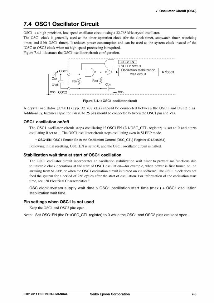
7 Oscillator Circuit (OSC)
S1C17611 TECHNICAL MANUAL Seiko Epson Corporation 7-5
7.4 OSC1 Oscillator CircuitOSC1 is a high-precision, low-speed oscillator circuit using a 32.768 kHz crystal oscillator.The OSC1 clock is generally used as the timer operation clock (for the clock timer, stopwatch timer, watchdog timer, and 8-bit OSC1 timer). It reduces power consumption and can be used as the system clock instead of the IOSC or OSC3 clock when no high-speed processing is required.Figure 7.4.1 illustrates the OSC1 oscillator circuit configuration.
VSS
OSC1
OSC1EN
CG1
SLEEP status
OSC2
X'tal1Rf1 RD1
CD1
VSS
fOSC1Oscillation stabilization
wait circuit
Figure 7.4.1: OSC1 oscillator circuit
A crystal oscillator (X’tal1) (Typ. 32.768 kHz) should be connected between the OSC1 and OSC2 pins. Additionally, trimmer capacitor CG1 (0 to 25 pF) should be connected between the OSC1 pin and VSS.
OSC1 oscillation on/off The OSC1 oscillator circuit stops oscillating if OSC1EN (D1/OSC_CTL register) is set to 0 and starts
oscillating if set to 1. The OSC1 oscillator circuit stops oscillating even in SLEEP mode.
* OSC1EN: OSC1 Enable Bit in the Oscillation Control (OSC_CTL) Register (D1/0x5061)
Following initial resetting, OSC1EN is set to 0, and the OSC1 oscillator circuit is halted.
Stabilization wait time at start of OSC1 oscillation The OSC1 oscillator circuit incorporates an oscillation stabilization wait timer to prevent malfunctions due
to unstable clock operations at the start of OSC1 oscillation—for example, when power is first turned on, on awaking from SLEEP, or when the OSC1 oscillation circuit is turned on via software. The OSC1 clock does not feed the system for a period of 256 cycles after the start of oscillation. For information of the oscillation start time, see “28 Electrical Characteristics.”
OSC clock system supply wait time ≤ OSC1 oscillation start time (max.) + OSC1 oscillation stabilization wait time.
Pin settings when OSC1 is not used Keep the OSC1 and OSC2 pins open.
Note: Set OSC1EN (the D1/OSC_CTL register) to 0 while the OSC1 and OSC2 pins are kept open.

7 Oscillator Circuit (OSC)
7-6 Seiko Epson Corporation S1C17611 TECHNICAL MANUAL
7.5 Clock SwitchingThe system clock select section of the S1C17611 consists of dual stages, high-speed clock (HSCLK) select and OSC1-HSCLK select. Figure 7.5.1 shows the configuration of the system clock select section.
HSCLKSEL
HSCLK
CLKSRC
System clock
P01MUX[1:0]
EXOSC3
OSC3
IOSC
OSC1
Figure 7.5.1: System clock select section
High-speed Clock (HSCLK) SelectionThe S1C17611 includes the IOSC and OSC3 oscillator circuits to generate high-speed clocks (HSCLK). The IOSC oscillator circuit is turned on, and the IOSC clock is selected for HSCLK when operation starts after the initial reset. To select OSC3 for HSCLK, turn on the OSC3 oscillator circuit (see section 7.3), and then write 1 to HSCLKSEL (D1/OSC_SRC register). To select IOSC for HSCLK, turn on the IOSC oscillator circuit (see section 7.2), and then write 0 to HSCLKSEL.
* HSCLKSEL: High-speed Clock Select Bit in the Clock Source Select (OSC_SRC) Register (D1/0x5060)
Note: To select HSCLK, both of the IOSC and OSC3 must be turned on. Writing to HSCLKSEL while both of them are not turned on does not switch HSCLK, and does not change the HSCLKSEL value.
OSC1 HSCLK selectionThe S1C17611 includes the OSC1 oscillator circuit to generate low-speed clocks. Either of the OSC1 or HSCLK can be selected for the system clock. HSCLK is selected when operation starts after the initial reset.To select OSC1 for the system clock, turn on the OSC1 oscillator circuit (see section 7.4), and then write 1 to CLKSRC (D0/OSC_SRC register). To select HSCLK for the system clock, write 0 to CLKSRC (D0/OSC_SRC register) while HSCLK is operating.It takes one HSCLK cycle at minimum or one OSC1 cycle at maximum to switch clocks from OSC1 to HSCLK and vice versa.
* CLKSRC: System Clock Source Select Bit in the Clock Source Select (OSC_SRC) Register (D0/0x5060)
Oscillator circuits other than selected for the system clock and are not used as the operating clock for peripheral circuits can be stopped to reduce current consumption.
Notes: • To select OSC1_HSCLK, both of the OSC1 and HSCLK must be operating. Writing to CLKSRC while one of them is not operating does not switch the system clock, and does not change the CLKSRC value.
The table 7.5.1 shows combinations of register settings permitted to select OSC1-HSCLK.
Table 7.5.1: Combinations of settings permitted to select OSC1-HSCLK
IOSC OSC3 EXOSC3 OSC1 System clockOn On Off On IOSC, OSC3, or OSC1On Off On On IOSC, EXOSC3, or OSC1On Off Off On IOSC or OSC1Off On Off On OSC3 or OSC1Off Off On On EXOSC3 or OSC1

7 Oscillator Circuit (OSC)
S1C17611 TECHNICAL MANUAL Seiko Epson Corporation 7-7
• The oscillator circuit selected for the system clock cannot be turned off. • Sequential access of write/read to the CLKSRC register is prohibited. Between write and
read access instructions to CLKSRC, insert at least one instruction unrelated to access to the CLKSRC register.

7 Oscillator Circuit (OSC)
7-8 Seiko Epson Corporation S1C17611 TECHNICAL MANUAL
7.6 LCD Clock ControlThe OSC module incorporates an LCD clock generator for generating the LCD driver operating clock (LCLK). For specific information on the LCD driver, see “22 LCD Driver (LCD8).”
LCD driverOSC1 clock
HSCLK clock
Clock source selection
LCLK
Division ratio selection
On/off control
GateDivision circuit(1/32 to 1/512)
Figure 7.6.1: LCD clock generator
Clock source selection Use LCKSRC (D1/OSC_LCLK register) to select whether OSC1 or HSCLK is used to generate the LCD clock.
OSC1 is selected when LCKSRC is 1 (default), while HSCLK is selected when set to 0.
* LCKSRC: LCD Clock Source Select Bit in the LCD Clock Setup (OSC_LCLK) Register (D1/0x5063)
Clock division ratio selection OSC1 clock
No division ratio needs to be selected if OSC1 has been selected for the clock source. The OSC1 clock (Typ 32.768 kHz) is sent to the LCD driver unchanged.
HSCLK clock If HSCLK has been selected for the clock source, use LCKDV[2:0] (D[4:2]/OSC_LCLK register) to select
the division ratio.
* LCKDV[2:0]: LCD Clock Division Ratio Select Bits in the LCD Clock Setup (OSC_LCLK) Register (D[4:2]/0x5063)
Table 7.6.1: LCD clock division ratio selection
LCKDV[2:0] Division ratio0x7 to 0x5 Reserved
0x4 HSCLK•1/5120x3 HSCLK•1/2560x2 HSCLK•1/1280x1 HSCLK•1/640x0 HSCLK•1/32
(Default: 0x0)
Clock feed control Clock feed to the LCD driver is controlled using LCKEN (D0/OSC_LCLK register). The LCKEN default setting is 0, which stops the clock feed. Setting LCKEN to 1 sends the clock generated as
above to the LCD driver. If no LCD display is required, stop the clock feed to minimize current consumption.
* LCKEN: LCD Clock Enable Bit in the LCD Clock Setup (OSC_LCLK) Register (D0/0x5063)
Note: Change of clock source selection (LCKSRC (D1/0x5063)) and clock division ratio selection (LCKDV [2:0](D[4:2]/0x5063)) should be executed when LCKEN(D0/0x5063) is 0 and the clock to LCD driver is in “Stop” state.

7 Oscillator Circuit (OSC)
S1C17611 TECHNICAL MANUAL Seiko Epson Corporation 7-9
7.7 8-bit OSC1 Timer Clock ControlThe OSC module consists of a division circuit for generating the 8-bit OSC1 timer operation clock and a device for controlling the feed. The 8-bit OSC1 timer is a programmable timer that operates only using the OSC1 division clock. For detailed information, refer to “14 8-bit OSC1 Timer (T8OSC1).”
OSC1 clock 8-bit OSC1 timer
Division ratio selection On/off control
Division circuit(1/1 to 1/32)
Gate
Figure 7.7.1: 8-bit OSC1 timer clock control circuit
Clock division ratio selection Select the OSC1 clock division ratio using T8O1CK[2:0] (D[3:1]/OSC_T8OSC1 register)
* T8O1CK[2:0]: T8OSC1 Clock Division Ratio Select Bits in the T8OSC1 Clock Control (OSC_T8OSC1) Register (D[3:1]/0x5065)
Table 7.7.1: T8OSC1 clock division ratio selection
T8O1CK[2:0] Division ratio0x7 to 0x6 Reserved
0x5 OSC1•1/320x4 OSC1•1/160x3 OSC1•1/80x2 OSC1•1/40x1 OSC1•1/20x0 OSC1•1/1
(Default: 0x0)
Clock feed control The clock feed to the 8-bit OSC1 timer is controlled using T8O1CE (D0/OSC_T8OSC1 register). The T8O1CE default setting is 0, which stops the clock feed. Setting T8O1CE to 1 sends the clock generated as
above to the 8-bit OSC1 timer. Stop the clock feed to reduce power consumption if 8-bit OSC1 timer operation is not required.
* T8O1CE: T8OSC1 Clock Enable Bit in the T8OSC1 Clock Control (OSC_T8OSC1) Register (D0/0x5065)
Note: Change of clock division ratio selection (T8O1CK [2:0](D[3:1]/0x5065)) should be executed when T8O1CE(D0/0x5065) is 0 and the clock to 8-bit OSC1 timer is in “Stop” state.

7 Oscillator Circuit (OSC)
7-10 Seiko Epson Corporation S1C17611 TECHNICAL MANUAL
7.8 SVD Clock ControlThe OSC module consists of a division circuit for generating the SVD operation clock and a device for controlling the feed. For detailed information about SVD, refer to “25 Power Supply Voltage Detection Circuit (SVD)”.
OSC1
HSCLK
Clock source selection
On/off control
Gate SVDDivision circuit(1/512)
Figure 7.8.1: SVD Clock Generator
Clock selection Use SVDSRC (D1/OSC_SVD register) to select whether OSC1 or HSCLK/512 division is used to generate the
SVD clock. OSC1 is selected when SVDSRC is 1 (default), while 1/512 division of HSCLK is selected when it is set to 0.
* SVDSRC: SVD Clock Source Select Bit in the SVD Clock Setup (OSC_SVD) Register (D1/0x5066)
Clock feed control The clock feed to SVD is controlled using SVDCKEN (D0/OSC_SVD register). The SVDCKEN default
setting is 0, which stops the clock feed. Setting SVDCKEN to 1 sends the clock generated as above to the SVD. Stop the clock feed to reduce power consumption if SVD operation is not required.
* SVDCKEN: SVD Clock Enable Bit in the SVD Clock Control (OSC_SVD) Register (D0/0x5066)
Note: Change of clock selection (SVDSRC (D1/0x5066)) should be executed when SVDCKEN (D0/0x5066)is 0 and the clock to SVD is in “Stop” state.

7 Oscillator Circuit (OSC)
S1C17611 TECHNICAL MANUAL Seiko Epson Corporation 7-11
7.9 RFC Clock Control The OSC module consists of division circuit for generating Time Base Counter Clock (TCCLK) in the R/F converter and a device for controlling the feed. For detailed information about RFC, refer to “24 R/F Converter (RFC)”
OSC1
HSCLKTCCLK
Clock source selection On/Off control
Gate RFCDivision circuit(1/1 to 1/8)
Division ratio selection
Figure 7.9.1: RFC clock generator
Master clock selection Use RFTCKSRC (D1/OSC_RFC register) to select whether OSC1 or HSCLK is used to generate RFC clock.
OSC1 is selected when RFTCKSRC is 1 (default), while HSCLK is selected when it is set to 0.
* RFTCKSRC: RFC Clock Source Select Bit in the RFC Clock setup (OSC_RFC) Register (D1/0x5067)
Clock division ratio selection OSC1 clock
No division ratio needs to be selected if OSC1 has been selected for the clock source. The OSC1 clock (Typ 32.768 kHz) is sent to the R/F converter.
HSCLK clock If HSCLK has been selected for the clock source, use RFTCKDV[1:0] (D[4:2]/OSC_RFC register) to select
the division ratio.
* RFTCKDV[1:0]: RFC Clock Division Ratio Select Bits in the RFC Clock Setup (OSC_RFC) Register (D[3:2]/0x5067)
Table 7.9.1: RFC clock division ratio selection
RFTCKDV[1:0] Division ratio0x3 HSCLK•1/80x2 HSCLK•1/40x1 HSCLK•1/20x0 HSCLK•1/1
(Default: 0x0)
Clock feed control Clock feed to the RFC is controlled using RFTCKEN (D0/OSC_RFC register). The RFTCKEN default setting
is 0, which stops the clock feed. Setting RFTCKEN to 1 sends the clock generated as above to the RFC. If no RFC operation is required, stop the clock feed to reduce current consumption.
* RFTCKEN: RFC Clock Enable Bit in the RFC Clock control (OSC_RFC) Register (D0/0x5067)
Note: Change of master clock selection (RFTCKSRC (D1/0x5067)) and clock division ratio selection (RFTCKDV [1:0](D[3:2]/0x5067)) should be executed when RFTCKEN (D0/0x5067) is 0 and clock to RFC is in “Stop” state.

7 Oscillator Circuit (OSC)
7-12 Seiko Epson Corporation S1C17611 TECHNICAL MANUAL
7.10 Clock External Output (FOUTH, FOUT1)The HSCLK division clock (FOUTH) and OSC1 clock (FOUT1) can be output to devices outside the chip.
Division circuit(1/1 to 1/4)
I/O port (FOUTH pin)HSCLK clock
FOUTHOutput circuit
I/O port
On/off control function selection
function selection
Division ratio selection
I/O port (FOUT1 pin)OSC1 clock
FOUT1Output circuit
I/O port
On/off control
Figure 7.10.1: Clock output circuit
FOUTH output FOUTH is the HSCLK division clock.
Output pin setting The FOUTH output pin is combined with the input/output port. This functions as the input/output port
pin by default, so the pin function should be changed if use is required for CLOCK output. For more information on the selection methods of FOUTH pins and pin function, see “10 Input/Output Port (P).”
FOUTH clock frequency selection Three different clock output frequencies can be selected. Select the division ratio for the HSCLK clock
using FOUTHD[1:0] (D[3:2]/OSC_FOUT register).
* FOUTHD[1:0]: FOUTH Clock Division Ratio Select Bits in the FOUT Control (OSC_FOUT) Register (D[3:2]/0x5064)
Table 7.10.1: FOUTH clock division ratio selection
FOUTHD[1:0] Division ratio0x3 Reserved0x2 HSCLK•1/40x1 HSCLK•1/20x0 HSCLK•1/1
(Default: 0x0)
Clock output control The clock output is controlled using the FOUTHE (D1/OSC_FOUT register). Setting FOUTHE to 1 outputs
the FOUTH clock from the FOUTH pin. Setting it to 0 halts output.
* FOUTHE: FOUTH Output Enable Bit in the FOUT Control (OSC_FOUT) Register (D1/0x5064)
FOUTHE
FOUTH output
0 01
Figure 7.10.2: FOUTH output
Notes: • Since the FOUTH signal is asynchronized with FOUTHE writing, switching output on or off will generate certain hazards.
• Change of the single selection (FOUTHD [1:0] (D[3:2]/0x5064)) of FOUTH clock frequency should be executed when FOUTHE (D1/0x5064) is 0 and clock output is in “Stop” status.

7 Oscillator Circuit (OSC)
S1C17611 TECHNICAL MANUAL Seiko Epson Corporation 7-13
FOUT1 output FOUT1 is the OSC1 clock.
Output pin setting The FOUT1 output pin is combined with the input/output port. This functions as the input/output port
pin by default, so the pin function should be changed if use is required for CLOCK output. For more information on the selection methods of FOUT1 pins and pin function, see “10 Input/Output Port (P).”
Clock output control The clock output is controlled using the FOUT1E (D0/OSC_FOUT register). Setting FOUT1E to 1 outputs
the FOUT1 clock from the FOUT1 pin. Setting it to 0 halts output.
* FOUT1E: FOUT1 Output Enable Bit in the FOUT Control (OSC_FOUT) Register (D1/0x5064)
FOUT1E
FOUT1 output
0 01
Figure 7.10.3: FOUT1 output
Note: Since the FOUT1 signal is asynchronized with FOUT1E writing, switching output on or off will generate certain hazards.

7 Oscillator Circuit (OSC)
7-14 Seiko Epson Corporation S1C17611 TECHNICAL MANUAL
7.11 RESET and NMI Input Noise FiltersIf RESET or NMI is made active by mistake by being affected by a noise, unnecessary reset or NMI process will beexecuted.To prevent this problem, the noise filter is installed. This can remove noises from the NMI or RESET request signalof the watchdog timer before they are input from the P0 port key input reset signal to the internal reset (S1C17 coreand peripheral circuit).Separate noise filters are used for each signal. You can select to use or bypass them individually. All are active immediately after the initial resetting.
RESET input noise filter: Filters noise when RSTFE (D1/OSC_NFEN register) = 1; bypassed when RSTFE = 0NMI input noise filter: Filters noise when NMIFE (D0/OSC_NFEN register) = 1; bypassed when NMIFE = 0
* RSTFE: Reset Noise Filter Enable Bit in the Noise Filter Enable (OSC_NFEN) Register (D1/0x5062)* NMIFE: NMI Noise Filter Enable Bit in the Noise Filter Enable (OSC_NFEN) Register (D0/0x5062)
Notes: • All noise filters should normally be enabled. • The S1C17611 does not feature external NMI input pins, but the watchdog timer NMI request
signal passes through these filters.

7 Oscillator Circuit (OSC)
S1C17611 TECHNICAL MANUAL Seiko Epson Corporation 7-15
7.12 Control Register Details
Table 7.12.1 OSC register listAddress Register name Function
0x5060 OSC_SRC Clock Source Select Register Clock source selection0x5061 OSC_CTL Oscillation Control Register Oscillation control0x5062 OSC_NFEN Noise Filter Enable Register Noise filter on/off0x5063 OSC_LCLK LCD Clock Setup Register LCD clock setting0x5064 OSC_FOUT FOUT Control Register Clock external output control0x5065 OSC_T8OSC1 T8OSC1 Clock Control Register 8-bit OSC1 timer clock setting0x5066 OSC_SVD SVD Clock Control Register SVD clock setting0x5067 OSC_RFC RF TC Clock Control Register RFC TC clock setting
The OSC module registers are described in detail below. These are 8-bit registers.
Note: When data is written to the registers, the “Reserved” bits must always be written as 0 and not 1.

7 Oscillator Circuit (OSC)
7-16 Seiko Epson Corporation S1C17611 TECHNICAL MANUAL
0x5060: Clock Source Select Register (OSC_SRC)Register name Address Bit Name Function Setting Init. R/W Remarks
Clock Source Select Register(OSC_SRC)
0x5060(8 bits)
D7–2 – reserved – – – 0 when being read.D1 HSCLKSEL High-speed clock select 1 OSC3 0 IOSC 0 R/WD0 CLKSRC System clock source select 1 OSC1 0 HSCLK 0 R/W
D[7:2] Reserved
D1 HSCLKSEL: High-speed Clock Select Bit Selects the high-speed clock (HSCLK). 1 (R/W): OSC3 0 (R/W): IOSC (default)
D0 CLKSRC: System Clock Source Select Bit Selects the system clock source. 1 (R/W): OSC1 0 (R/W): HSCLK (default)
HSCLK (IOSC or OSC3) is selected for normal (high-speed) operations. If the HSCLK clock is not required, OSC1 can be set as the system clock and HSCLK (IOSC or OSC3) stopped to reduce power consumption.
Notes: • If the system clock is switched from HSCLK to OSC1 immediately after starting OSC1 oscillation, the system clock will stop until the OSC1 clock starts up (for the OSC1 clock 256-cycle period).
• Continuous access of write and read to CLKSRC register (D0/0x5060) is prohibited. Enter at least one instruction that is not related to access to CLKSRC register between write and read.

7 Oscillator Circuit (OSC)
S1C17611 TECHNICAL MANUAL Seiko Epson Corporation 7-17
0x5061: Oscillation Control Register (OSC_CTL)Register name Address Bit Name Function Setting Init. R/W Remarks
Oscillation Control Register(OSC_CTL)
0x5061(8 bits)
D7–6 IOSCWT[1:0] IOSC wait cycle select IOSCWT[1:0] Wait cycle 0x0 R/W0x30x20x10x0
8 cycles16 cycles32 cycles64 cycles
D5–4 OSC3WT[1:0] OSC3 wait cycle select OSC3WT[1:0] Wait cycle 0x0 R/W0x30x20x10x0
128 cycles256 cycles512 cycles
1024 cyclesD3 – reserved – – – 0 when being read.D2 IOSCEN IOSC enable 1 Enable 0 Disable 1 R/WD1 OSC1EN OSC1 enable 1 Enable 0 Disable 0 R/WD0 OSC3EN OSC3 enable 1 Enable 0 Disable 0 R/W
D[7:6] IOSCWT[1:0]: IOSC Wait Cycle Select Bits An oscillation stabilization wait time is set to prevent malfunctions due to unstable clock operations
when IOSC oscillation begins. The IOSC clock is not fed to the system immediately after IOSC oscillation starts—e.g., when power is
first turned on, when waking from SLEEP, or the IOSC oscillation circuit is switched on via software, until the time set here has elapsed.
Table 7.12.2: IOSC oscillation stabilization wait time settings
IOSCWT[1:0] Oscillation stabilization wait time0x3 8 cycles0x2 16 cycles0x1 32 cycles0x0 64 cycles
(Default: 0x0)
Since this is set to 64 cycles (IOSC clock) after initial resetting, the CPU does not begin operating immediately after resetting until this time has elapsed.
D[5:4] OSC3WT[1:0]: OSC3 Wait Cycle Select Bits An oscillation stabilization wait timer is set to prevent malfunctions due to unstable clock operation at
the start of OSC3 oscillation. The OSC3 clock is not fed to the system immediately after OSC3 oscillation starts—for example, when
power is first turned on, on awaking from SLEEP, or when the OSC3 oscillation circuit is turned on via software—until the time set here has elapsed.
Table 7.12.3: OSC3 oscillation stabilization wait time settings
OSC3WT[1:0] Oscillation stabilization wait time0x3 128 cycles0x2 256 cycles0x1 512 cycles0x0 1,024 cycles
(Default: 0x0)
This is set to 1,024 cycles (OSC3 clock) after initial resetting.
Note: The OSC3 oscillation start time depends on the oscillator and externally connected components. The time should be set with an adequate oscillation stabilization wait time. Refer to the typical oscillation start times specified in “28 Electrical Characteristics.”
D3 Reserved

7 Oscillator Circuit (OSC)
7-18 Seiko Epson Corporation S1C17611 TECHNICAL MANUAL
D2 IOSCEN: IOSC Enable Bit Permits or prevents IOSC oscillator circuit operation. 1 (R/W): Permitted (on) (default) 0 (R/W): Prohibited (off)
Note: The IOSC oscillator circuit cannot be stopped if the IOSC clock is being used as the system clock.
D1 OSC1EN: OSC1 Enable Bit Permits or prohibits OSC1 oscillator circuit operation. 1 (R/W): Permitted (on) 0 (R/W): Prohibited (off) (default)
Notes: • The OSC1 oscillator circuit cannot be stopped if the OSC1 clock is being used as the system clock.
• The OSC1 clock is not fed to the system for 256 cycles to prevent malfunctions immediately after OSC1 oscillation is started by changing the OSC1EN setting from 0 to 1.
D0 OSC3EN: OSC3 Enable Bit Permits or prohibits OSC3 oscillator circuit operation. 1 (R/W): Permitted (on) 0 (R/W): Prohibited (off) (default)
Note: The OSC3 oscillator circuit cannot be stopped if the OSC3 clock is being used as the system clock.

7 Oscillator Circuit (OSC)
S1C17611 TECHNICAL MANUAL Seiko Epson Corporation 7-19
0x5062: Noise Filter Enable Register (OSC_NFEN)Register name Address Bit Name Function Setting Init. R/W Remarks
Noise Filter Enable Register(OSC_NFEN)
0x5062(8 bits)
D7–2 – reserved – – – 0 when being read.D1 RSTFE Reset noise filter enable 1 Enable 0 Disable 1 R/WD0 NMIFE NMI noise filter enable 1 Enable 0 Disable 0 R/W
D[7:2] Reserved
D1 RSTFE: Reset Noise Filter Enable Bit Enables or disables the RESET input noise filter. 1 (R/W): Enabled (noise filtering) (default) 0 (R/W): Disabled (bypass)
D0 NMIFE: NMI Noise Filter Enable Bit Enables or disables the NMI input noise filter. 1 (R/W): Enabled (noise filtering) 0 (R/W): Disabled (bypass) (default)
Note: The S1C17611 does not feature external NMI input pins, but the watchdog timer NMI request signal passes through these filters.
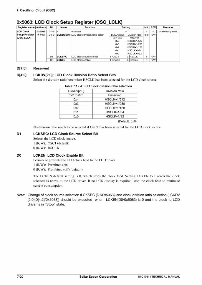
7 Oscillator Circuit (OSC)
7-20 Seiko Epson Corporation S1C17611 TECHNICAL MANUAL
0x5063: LCD Clock Setup Register (OSC_LCLK)Register name Address Bit Name Function Setting Init. R/W Remarks
LCD Clock Setup Register(OSC_LCLK)
0x5063(8 bits)
D7–5 – reserved – – – 0 when being read.D4–2 LCKDV[2:0] LCD clock division ratio select LCKDV[2:0] Division ratio 0x0 R/W
0x7–0x50x40x30x20x10x0
reservedHSCLK•1/512HSCLK•1/256HSCLK•1/128HSCLK•1/64HSCLK•1/32
D1 LCKSRC LCD clock source select 1 OSC1 0 HSCLK 1 R/WD0 LCKEN LCD clock enable 1 Enable 0 Disable 0 R/W
D[7:5] Reserved
D[4:2] LCKDV[2:0]: LCD Clock Division Ratio Select Bits Select the division ratio here when HSCLK has been selected for the LCD clock source.
Table 7.12.4: LCD clock division ratio selection
LCKDV[2:0] Division ratio0x7 to 0x5 Reserved
0x4 HSCLK•1/5120x3 HSCLK•1/2560x2 HSCLK•1/1280x1 HSCLK•1/640x0 HSCLK•1/32
(Default: 0x0)
No division ratio needs to be selected if OSC1 has been selected for the LCD clock source.
D1 LCKSRC: LCD Clock Source Select Bit Selects the LCD clock source. 1 (R/W): OSC1 (default) 0 (R/W): HSCLK
D0 LCKEN: LCD Clock Enable Bit Permits or prevents the LCD clock feed to the LCD driver. 1 (R/W): Permitted (on) 0 (R/W): Prohibited (off) (default)
The LCKEN default setting is 0, which stops the clock feed. Setting LCKEN to 1 sends the clock selected as above to the LCD driver. If no LCD display is required, stop the clock feed to minimize current consumption.
Note: Change of clock source selection (LCKSRC (D1/0x5063)) and clock division ratio selection (LCKDV [2:0](D[4:2]/0x5063)) should be executed when LCKEN(D0/0x5063) is 0 and the clock to LCD driver is in “Stop” state.

7 Oscillator Circuit (OSC)
S1C17611 TECHNICAL MANUAL Seiko Epson Corporation 7-21
0x5064: FOUT Control Register (OSC_FOUT)Register name Address Bit Name Function Setting Init. R/W Remarks
FOUT Control Register(OSC_FOUT)
0x5064(8 bits)
D7–4 – reserved – – – 0 when being read.D3–2 FOUTHD[1:0] FOUTH clock division ratio select FOUTHD[1:0] Division ratio 0x0 R/W
0x30x20x10x0
reservedHSCLK•1/4HSCLK•1/2HSCLK•1/1
D1 FOUTHE FOUTH output enable 1 Enable 0 Disable 0 R/WD0 FOUT1E FOUT1 output enable 1 Enable 0 Disable 0 R/W
D[7:4] Reserved
D[3:2] FOUTHD[1:0]: FOUTH Clock Division Ratio Select Bits Select the HSCLK clock division ratio to set the FOUTH clock frequency.
Table 7.12.5: FOUTH clock division ratio selection
FOUTHD[1:0] Division ratio0x3 Reserved0x2 HSCLK•1/40x1 HSCLK•1/20x0 HSCLK•1/1
(Default: 0x0)
D1 FOUTHE: FOUTH Output Enable Bit Permits or prohibits FOUTH clock (HSCLK division clock) external output. 1 (R/W): Permitted (on) 0 (R/W): Prohibited (off) (default)
Setting FOUTHE to 1 outputs the FOUTH clock from the FOUTH pin. Setting it to 0 stops the output.
D0 FOUT1E: FOUT1 Output Enable Bit Permits or prohibits FOUT1 clock (OSC1 clock) external output. 1 (R/W): Permitted (on) 0 (R/W): Prohibited (off) (default)
Setting FOUT1E to 1 outputs the FOUT1 clock from the FOUT1 pin. Setting it to 0 stops the output.
Note: Change of the clock division ratio selection should be executed when FOUTHE (D1/0x5064) is 0 and clock output is in “Stop” status.

7 Oscillator Circuit (OSC)
7-22 Seiko Epson Corporation S1C17611 TECHNICAL MANUAL
0x5065: T8OSC1 Clock Control Register (OSC_T8OSC1)Register name Address Bit Name Function Setting Init. R/W Remarks
T8OSC1 Clock Control Register(OSC_T8OSC1)
0x5065(8 bits)
D7–4 – reserved – – – 0 when being read.D3–1 T8O1CK[2:0] T8OSC1 clock division ratio select T8O1CK[2:0] Division ratio 0x0 R/W
0x7–0x60x50x40x30x20x10x0
reservedOSC1•1/32OSC1•1/16OSC1•1/8OSC1•1/4OSC1•1/2OSC1•1/1
D0 T8O1CE T8OSC1 clock output enable 1 Enable 0 Disable 0 R/W
D[7:4] Reserved
D[3:1] T8O1CK[2:0]: T8OSC1 Clock Division Ratio Select Bits Select the OSC1 clock division ratio and set the 8-bit OSC1 timer operation clock.
Table 7.12.6: T8OSC1 clock division ratio selection
T8O1CK[2:0] Division ratio0x7 to 0x6 Reserved
0x5 OSC1•1/320x4 OSC1•1/160x3 OSC1•1/80x2 OSC1•1/40x1 OSC1•1/20x0 OSC1•1/1
(Default: 0x0)
D0 T8O1CE: T8OSC1 Clock Output Enable Bit Permits or prohibits clock feed to the 8-bit OSC1 timer. 1 (R/W): Permitted (on) 0 (R/W): Prohibited (off) (default)
The T8O1CE default setting is 0, which stops the clock feed. Setting T8O1CE to 1 sends the clock selected by the above bit to the 8-bit OSC1 timer. Stop the clock feed to reduce power consumption if 8-bit OSC1 timer operation is not required.
Note: Change of clock division ratio selection (T8O1CK [2:0](D[3:1]/0x5065)) should be executed when T8O1CE(D0/0x5065) is 0 and the clock to 8-bit OSC1 timer is in “Stop” state.

7 Oscillator Circuit (OSC)
S1C17611 TECHNICAL MANUAL Seiko Epson Corporation 7-23
0x5066: SVD Clock Control Register (OSC_SVD)Register name Address Bit Name Function Setting Init. R/W Remarks
SVD Clock Control Register (OSC_SVD)
0x5066(8 bits)
D7–2 – reserved – – – 0 when being read.D1 SVDSRC SVD clock source select 1 OSC1 0 HSCLK•
1/5121 R/W
D0 SVDCKEN SVD clock enable 1 Enable 0 Disable 0 R/W
D[7:2] Reserved
D1 SVDSRC: SVD Clock Source Select Bit Selects the SVD clock source. 1 (R/W): OSC1 (default) 0 (R/W): HSCLK•1/512
D0 SVDCKEN: SVD Clock Enable Bit Permits or prevents the SVD clock feed to the SVD. 1 (R/W): Permitted (on) 0 (R/W): Prohibited (off) (default) The SVDCKEN default setting is 0, which stops the clock feed. Setting SVDCKEN to 1 sends the
clock selected by the above bit to the SVD. Stop the clock feed to reduce power consumption if SVD operation is not required.
Note: Change of clock selection (SVDSRC (D1/0x5066)) should be executed when SVDKEN (D0/0x5066) is 0 and the clock to SVD is in “Stop” status.

7 Oscillator Circuit (OSC)
7-24 Seiko Epson Corporation S1C17611 TECHNICAL MANUAL
0x5067: RFC Clock Control Register (OSC_RFTCK)Register name Address Bit Name Function Setting Init. R/W Remarks
RFC Clock Control Register(OSC_RFTCK)
0x5067(8 bits)
D7–4 – reserved – – – 0 when being read.D3–2 RFTCKDV
[1:0]RFC TC clock division ratio select RFCDV[1:0] Division ratio 0x0 R/W
0x30x20x10x0
HSCLK•1/8HSCLK•1/4HSCLK•1/2HSCLK•1/1
D1 RFTCKSRC RFC TC clock source select 1 OSC1 0 HSCLK 1 R/WD0 RFTCKEN RFC TC clock enable 1 Enable 0 Disable 0 R/W
D[7:4] Reserved
D[3:2] RFTCKDV [1:0]: RFC TC Clock Division Ratio Select Bits Select the division ratio here when HSCLK has been selected for the RFC TC clock source.
Table 7.12.7: RFC TC clock division ratio selection
RFTCKDV[1:0] Division ratio0x3 HSCLK•1/80x2 HSCLK•1/40x1 HSCLK•1/20x0 HSCLK•1/1
(Default: 0x0)
No division ratio needs to be selected if OSC1 has been selected for the RFC clock source.
D1 RFTCKSRC: RFC TC Clock Source Select Bit Selects the RFC TC clock source. 1 (R/W): OSC1 (default) 0 (R/W): HSCLK
D0 RFTCKEN: RFC TC Clock Enable Bit Permits or prevents the RFC TC clock feed to the RFC. 1 (R/W): Permitted (on) 0 (R/W): Prohibited (off) (default)
The RFTCKEN default setting is 0, which stops the clock feed. Setting RFTCKEN to 1 sends the clock selected as above to the RFC driver. If no R/F conversion is required, stop the clock feed to minimize current consumption.
Note: Change of master clock selection (RFTCKSRC (D1/0x5067)) and clock division ratio selection (RFTCKDV [1:0] (D[3:2]/0x5067) should be executed when RFTCKEN (D0/0x5067) is 0 and the clock to RFC is in “Stop” status.

7 Oscillator Circuit (OSC)
S1C17611 TECHNICAL MANUAL Seiko Epson Corporation 7-25
7.13 Precautions• The oscillation start time depends on the oscillator and externally connected components. The time should be set
with an adequate OSC3 oscillation stabilization wait time. Refer to the typical oscillation start times specified in “28 Electrical Characteristics.”
• Switching the system clock from HSCLK to OSC1 immediately after starting OSC1 oscillation will stop the system clock until the OSC1 clock starts up (for the OSC1 clock 256-cycle period).
• The IOSC oscillator circuit cannot be stopped if the IOSC clock is being used as the system clock.
• The OSC3 oscillator circuit cannot be stopped if the OSC3 clock is being used as the system clock.
• The OSC1 oscillator circuit cannot be stopped if the OSC1 clock is being used as the system clock.
• Since the FOUTH/FOUT1 signal is asynchronized with FOUTHE/FOUT1E writing, switching output on or off will generate certain hazards.
• Continuous access of write and read to CLKSRC register (D0/0x5060) is prohibited. Enter at least one instruction that is not related to access to CLKSRC register between write and read.
• Change of clock source selection (LCKSRC (D1/0x5063)) and clock division ratio selection (LCKDV [2:0](D[4:2]/0x5063)) should be executed when LCKEN(D0/0x5063) is 0 and the clock to LCD driver is in “Stop” state.
• Change of clock division ratio selection (T8O1CK [2:0](D[3:1]/0x5065)) should be executed when T8O1CE(D0/0x5065) is 0 and the clock to 8-bit OSC1 timer is in “Stop” state.
• Change of clock selection (SVDSRC (D1/0x5066)) should be executed when SVDCKEN (D0/0x5066)is 0 and the clock to SVD is in “Stop” state.
• Change of master clock selection (RFTCKSRC (D1/0x5067)) and clock division ratio selection (RFTCKDV [1:0](D[3:2]/0x5067)) should be executed when RFTCKEN (D0/0x5067) is 0 and clock to RFC is in “Stop” state.
• Change of the single selection (FOUTHD [1:0] (D[3:2]/0x5064) of FOUTH clock frequency should be executed when FOUTHE (D1/0x5064) is 0 and clock output is in “Stop” status.
• The stability of oscillation depends on the oscillator and external add-on components. Full evaluation is required for configuring shorter stabilization wait time.
OSC3 clock system supply wait time ≤ OSC3 oscillation start time (max.) + OSC3 oscillation stabilization wait time.
• Set OSC3EN (the D0/OSC_CTL register) to 0 while the OSC3 and OSC4 pins are not used.
• Set OSC1EN (the D1/OSC_CTL register) to 0 while the OSC1 and OSC2 pins are kept open.

8 Clock Generator (CLG)
S1C17611 TECHNICAL MANUAL Seiko Epson Corporation 8-1
8 Clock Generator (CLG)
8.1 Clock Generator ConfigurationThe clock generator controls the system clock feed to the S1C17 core and peripheral modules.Figure 8.1.1 illustrates the clock system and CLG module configuration.
HSCLKCCLK
OSC1
IOSC
OSC1
FOUTHoutput circuit
OSC1oscillator circuit
Division circuit(1/1 to 1/4)
Clock gear(1/1 to 1/8)
Gate S1C17 core
BCLK
CLK_256Hz
Gate
FOUTH
FOUT1output circuitFOUT1
Noise filterRESET
OSC1
OSC2
HSCLK selection
Wait circuit for wakeup
wakeup
HALT
HALT
Division circuit(1/1 to 1/16K)
Noise filterNMI
CT, SWT, WDT
T8OSC1
Division circuit
(1/128)
(1/1 to 1/32)
Gate
Gate
CLG
PSC
OSC
PCLKGate
T8F, T16, T16E, P, UART, SPI, I2C (master), ADC
LCLK
OSC1
HSCLK
HSCLK
HSCLK
SVD
OSC1
LCD
OSC1
RFC
Division circuit(1/512)
Division circuit(1/32 to 1/512)
Division circuit(1/1 to 1/8)
Gate
Gate
Gate
Clock sourceselection
Clock source selection
Clock source selection
Clock source selection
Systemclock
Gear selection
S1C17 core
S1C17 core
Division ratioselection
Division ratioselection
Division ratioselection
Division ratio selection On/off control
SLEEP, on/off control
On/off control
On/off control
On/off control
On/off control
IOSCoscillator circuit
SLEEP, on/off control
On/off control
On/off control
On/off control
On/off control
On/off control
Internal bus, RAM,Flash, LCD display RAM, Control regiser (LCD, RFC)
T16, T8F, UART, SPI, I2C (master), T16E, P, MISC, VD1, SVD, ADC, I2C (slave)
OSC3
Wait circuit for wakeup
OSC3oscillator circuit
OSC3OSC4
EXOSC3
wakeupSLEEP, on/off control
Clock source selection
Figure 8.1.1: CLG module configuration
To reduce power consumption, control the clock in conjunction with processing and use standby mode. For more information on reducing power consumption, refer to “Appendix C: Power Saving.”

8 Clock Generator (CLG)
8-2 Seiko Epson Corporation S1C17611 TECHNICAL MANUAL
8.2 CPU Core Clock (CCLK) ControlThe CLG module incorporates a clock gear to slow down the system clock to send to the S1C17 core. To reduce power consumption, operate the S1C17 core with the slowest possible clock speed. The halt instruction can be executed to stop the clock feed from the CLG to the S1C17 core for power savings.
HSCLK CCLK
OSC1
Clock gear(1/1 to 1/8)
Gate S1C17 core
Gear selection
System clock
HALT
Figure 8.2.1: CCLK feed system
Clock gear settings CCLKGR[1:0] (D[1:0]/CLG_CCLK register) is used to select the gear ratio to reduce system clock speeds.
* CCLKGR[1:0]: CCLK Clock Gear Ratio Select Bits in the CCLK Control (CLG_CCLK) Register (D[1:0]/0x5081)
Table 8.2.1: CCLK gear ratio selection
CCLKGR[1:0] Gear ratio0x3 1/80x2 1/40x1 1/20x0 1/1
(Default: 0x0)
Clock feed control The CCLK clock feed is stopped by executing the halt instruction. Since this does not stop the system clock,
peripheral modules will continue to operate. HALT mode is cleared by resetting, NMI, or other interrupts. The CCLK feed resumes when HALT mode is
cleared. Executing the slp instruction suspends system clock feed to the CLG, thereby halting the CCLK feed as well.
Clearing SLEEP mode with an external interrupt restarts the system clock feed and the CCLK feed. For more information on system clock control, refer to “7 Oscillator Circuit (OSC).”

8 Clock Generator (CLG)
S1C17611 TECHNICAL MANUAL Seiko Epson Corporation 8-3
8.3 Peripheral Module Clock (PCLK) ControlThe CLG module also controls the clock feed to peripheral modules.The system clock is used unmodified for the peripheral module clock (PCLK).
Internal peripheral circuits• Prescaler• UART• 8-bit timer• 16-bit timer Ch.0 to 2• SPI• I2C (master/slave)• SVD circuit• Power supply control circuit• P port & port MUX• PWM timer Ch.0, Ch.1• MISC register• A/D converter
Gate
On/off control
PCLKHSCLK
OSC1
System clock
Figure 8.3.1: Peripheral module clock control circuit
Clock feed control PCLK feed is controlled by PCKEN[1:0] (D[1:0]/CLG_PCLK register).
* PCKEN[1:0]: PCLK Enable Bits in the PCLK Control (CLG_PCLK) Register (D[1:0]/0x5080)
Table 8.3.1: PCLK control
PCKEN[1:0] PCLK feed0x3 Permitted (on)0x2 Setting prohibited0x1 Setting prohibited0x0 Prohibited (off)
(Default: 0x3)
The default setting is 0x3, which enables the clock feed. Stop the clock feed to reduce power consumption unless all peripheral modules (modules listed above) within the internal peripheral circuit area need to be running.
Note: Do not set PCKEN[1:0] (D[1:0]/CLG_PCLK register) to 0x2 or 0x1, since doing so will stop the operation of certain peripheral modules.
Peripheral modules not operating on PCLK The OSC1 peripheral module operates using a clock other than PCLK. Therefore, PCLK is not required. The LCD driver and RFC also operate, including access to control registers, using a clock other than PCLK.
OSC1 peripheral module The clock timer, stopwatch timer, watchdog timer, and 8-bit OSC1 timer operate using the OSC1 division
clock.
LCD driver The LCD driver uses the LCLK clock originating from the HSCLK division clock or OSC1 clock. It also uses BCLK to access display memory. Therefore PCLK does not need to be turned on.
RFC RFC uses the TCCLK clock originating from the HSCLK division clock or OSC1 clock. Therefore PCLK
does not need to be turned on.

8 Clock Generator (CLG)
8-4 Seiko Epson Corporation S1C17611 TECHNICAL MANUAL
8.4 Control Register Details
Table 8.4.1 CLG register listAddress Register name Function
0x5080 CLG_PCLK PCLK Control Register PCLK feed control0x5081 CLG_CCLK CCLK Control Register CCLK division ratio setting
The CLG module registers are described in detail below. These are 8-bit registers.
Note: When data is written to the registers, the “Reserved” bits must always be written as 0 and not 1.

8 Clock Generator (CLG)
S1C17611 TECHNICAL MANUAL Seiko Epson Corporation 8-5
0x5080: PCLK Control Register (CLG_PCLK)Register name Address Bit Name Function Setting Init. R/W Remarks
PCLK Control Register(CLG_PCLK)
0x5080(8 bits)
D7–2 – reserved – – – 0 when being read.D1–0 PCKEN[1:0] PCLK enable PCKEN[1:0] PCLK supply 0x3 R/W
0x30x20x10x0
EnableNot allowedNot allowed
Disable
D[7:2] Reserved
D[1:0] PCKEN[1:0]: PCLK Enable Bits Permit or prohibit clock (PCLK) feed to internal peripheral modules.
Table 8.4.2: PCLK control
PCKEN[1:0] PCLK feed0x3 Permitted (on)0x2 Setting prohibited0x1 Setting prohibited0x0 Prohibited (off)
(Default: 0x3)
The PCKEN[1:0] default setting is 0x3, which enables clock feed. Stop the clock feed to reduce power consumption if the peripheral modules listed below are not required.
Peripheral modules operated using PCLK • Prescaler (PWM timer, P port) • UART • 8-bit timer • 16-bit timer Ch.0 to 2 • SPI • I2C (master/slave) • SVD circuit • Power supply control circuit • P port & port MUX • PWM timer Ch.0 to 1 • MISC register • A/D converter
The following peripheral modules operate, including access to control registers, using a clock other than PCLK. Therefore, PCLK does not need to be turned on.
• Clock timer • Stopwatch timer • Watchdog timer • 8-bit OSC1 timer • LCD driver • R/F converter
Note: Do not set PCKEN[1:0] to 0x2 or 0x1, since doing so will stop the operation of certain peripheral modules.
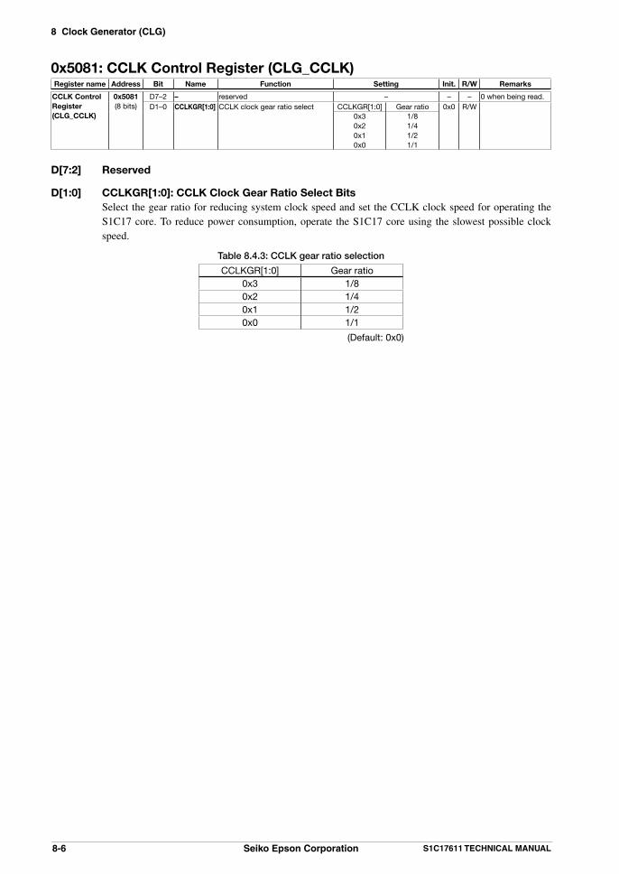
8 Clock Generator (CLG)
8-6 Seiko Epson Corporation S1C17611 TECHNICAL MANUAL
0x5081: CCLK Control Register (CLG_CCLK)Register name Address Bit Name Function Setting Init. R/W Remarks
CCLK Control Register(CLG_CCLK)
0x5081(8 bits)
D7–2 – reserved – – – 0 when being read.D1–0 CCLKGR[1:0] CCLK clock gear ratio select CCLKGR[1:0] Gear ratio 0x0 R/W
0x30x20x10x0
1/81/41/21/1
D[7:2] Reserved
D[1:0] CCLKGR[1:0]: CCLK Clock Gear Ratio Select Bits Select the gear ratio for reducing system clock speed and set the CCLK clock speed for operating the
S1C17 core. To reduce power consumption, operate the S1C17 core using the slowest possible clock speed.
Table 8.4.3: CCLK gear ratio selection
CCLKGR[1:0] Gear ratio0x3 1/80x2 1/40x1 1/20x0 1/1
(Default: 0x0)

8 Clock Generator (CLG)
S1C17611 TECHNICAL MANUAL Seiko Epson Corporation 8-7
8.5 Precautions(1) The default settings enable PCLK feed to peripheral modules. To reduce power consumption, stop the clock
feed if the peripheral modules listed below are not used.
Peripheral modules operated using PCLK • Prescaler (PWM timer, P port) • UART • 8-bit timer • 16-bit timer Ch.0 to 2 • SPI • I2C (master/slave) • SVD circuit • Power supply control circuit • P port & port MUX • PWM timer Ch.0 to 1 • MISC register • A/D converter
The following peripheral modules operate, including access to control registers, using a clock other than PCLK. Therefore, PCLK does not need to be turned on.
• Clock timer • Stopwatch timer • Watchdog timer • 8-bit OSC1 timer • LCD driver • R/F converter
(2) Do not set PCKEN[1:0] (D[1:0]/CLG_PCLK register) to 0x2 or 0x1, since doing so will stop the operation of certain peripheral modules.
* PCKEN[1:0]: PCLK Enable Bits in the PCLK Control (CLG_PCLK) Register (D[1:0]/0x5080)
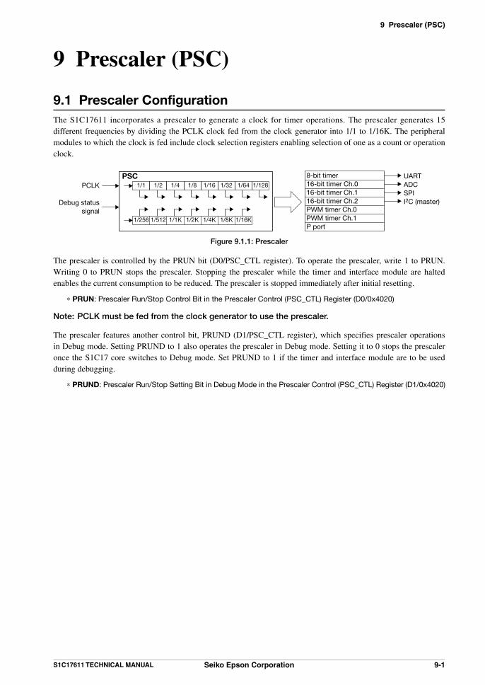
9 Prescaler (PSC)
S1C17611 TECHNICAL MANUAL Seiko Epson Corporation 9-1
9 Prescaler (PSC)
9.1 Prescaler ConfigurationThe S1C17611 incorporates a prescaler to generate a clock for timer operations. The prescaler generates 15 different frequencies by dividing the PCLK clock fed from the clock generator into 1/1 to 1/16K. The peripheral modules to which the clock is fed include clock selection registers enabling selection of one as a count or operation clock.
1/1PSC
1/2 1/4 1/8 1/16 1/32 1/64 1/128
1/256 1/512 1/1K 1/2K 1/4K 1/8K 1/16K
UARTADCSPII2C (master)
PCLK
Debug statussignal
8-bit timer16-bit timer Ch.016-bit timer Ch.116-bit timer Ch.2PWM timer Ch.0PWM timer Ch.1P port
Figure 9.1.1: Prescaler
The prescaler is controlled by the PRUN bit (D0/PSC_CTL register). To operate the prescaler, write 1 to PRUN. Writing 0 to PRUN stops the prescaler. Stopping the prescaler while the timer and interface module are halted enables the current consumption to be reduced. The prescaler is stopped immediately after initial resetting.
* PRUN: Prescaler Run/Stop Control Bit in the Prescaler Control (PSC_CTL) Register (D0/0x4020)
Note: PCLK must be fed from the clock generator to use the prescaler.
The prescaler features another control bit, PRUND (D1/PSC_CTL register), which specifies prescaler operations in Debug mode. Setting PRUND to 1 also operates the prescaler in Debug mode. Setting it to 0 stops the prescaler once the S1C17 core switches to Debug mode. Set PRUND to 1 if the timer and interface module are to be used during debugging.
* PRUND: Prescaler Run/Stop Setting Bit in Debug Mode in the Prescaler Control (PSC_CTL) Register (D1/0x4020)
9 Prescaler (PSC)
9-2 Seiko Epson Corporation S1C17611 TECHNICAL MANUAL
9.2 Control Register Details
Table 9.2.1: Prescaler registerAddress Register name Function
0x4020 PSC_CTL Prescaler Control Register Prescaler start/stop control
The prescaler register is an 8-bit register.
Note: When data is written to the registers, the “Reserved” bits must always be written as 0 and not 1.
0x4020: Prescaler Control Register (PSC_CTL)Register name Address Bit Name Function Setting Init. R/W Remarks
Prescaler Con-trol Register(PSC_CTL)
0x4020(8 bits)
D7–2 – reserved – – – 0 when being read.D1 PRUND Prescaler run/stop in debug mode 1 Run 0 Stop 0 R/WD0 PRUN Prescaler run/stop control 1 Run 0 Stop 0 R/W
D[7:2] Reserved
D1 PRUND: Prescaler Run/Stop Setting Bit for Debug Mode Selects prescaler operations in Debug mode. 1 (R/W): Operate 0 (R/W): Stop (default)
Setting PRUND to 1 operates the prescaler even in Debug mode. Setting it to 0 stops the prescaler once the S1C17 core switches to Debug mode. Set PRUND to 1 to use the timer and interface module during debugging.
D0 PRUN: Prescaler Run/Stop Control Bit Starts or stops prescaler operation. 1 (R/W): Start operation 0 (R/W): Stop (default)
Write 1 to PRUN to operate the prescaler. Write 0 to PRUN to stop the prescaler. To reduce current consumption, stop the prescaler if the timer and interface module are already stopped.
9 Prescaler (PSC)
S1C17611 TECHNICAL MANUAL Seiko Epson Corporation 9-3
9.3 PrecautionsPCLK must be fed from the clock generator to use the prescaler.

10 Input/Output Port (P)
S1C17611 TECHNICAL MANUAL Seiko Epson Corporation 10-1
10 Input/Output Port (P)
10.1 Input/Output Port ConfigurationThe S1C17611 includes 19 input/output ports (P0[7:0], P1[7:0], P2[2:0]) to allow software switching of input/output direction. These share internal peripheral module input/output pins (with certain exceptions), but pins not used for peripheral modules can be used as general purpose input/output ports.Figure 10.1.1 illustrates the input/output port configuration.
VDD
VSS
Pxy
PxPUy
PxOENy
PxSMy
PxOUTy
PxyMUX
Schmitt trigger control
PxIENyInput enable
Inte
rnal
dat
a b
us
Peripheral module input
Peripheral module output
Peripheral module I/O control
Pull-up enable
Output enable
Output data
Function selection
Figure 10.1.1: Input/output port configuration
The P0 and P1 ports can generate input interrupts.The P0[5:2] port can be used for key entry resets. (For more information, refer to “5.1.2 P0 Port Key Entry Reset.”)
Note: The PCLK clock must be fed from the clock generator to access the input/output port. The prescaler output clock is also needed to operate the P0/P1 port chattering filter. Switch
on the prescaler when using this function.

10 Input/Output Port (P)
10-2 Seiko Epson Corporation S1C17611 TECHNICAL MANUAL
10.2 Input/Output Pin Function Selection (Port MUX)The input/output port pins share peripheral module input/output pins (with certain exceptions). Each pin can be set for use as an input/output port or for peripheral modules via the corresponding port function selection bits for each port. Pins not used for peripheral modules can be used as general purpose input/output ports.
Table 10.2.1: Input/output pin function selectionPin function 0PxxMUX = 0
Pin function 1PxxMUX = 1
Pin function 2PxxMUX = 2
Pin function 3PxxMUX = 3
Port function selection bit
Control register
P00 OSC4 FOUT1 (CLG) − P00MUX (D1-0) P0 Port Function Select(P0_PMUX) Register (0x52a0)
P01 OSC3 EXOSC3 − P01MUX (D3-2)P02 TOUT5 (T8OSC1) RFCLKO (RFC) − P02MUX (D5-4)P03 AIN3 (ADC10SA) SCL0 (I2CM) SCL1 (I2CS) P03MUX (D7-6)P04 AIN2 (ADC10SA) SDA0 (I2CM) SDA1 (I2CS) P04MUX (D1-0) P0 Port Function Select
(P0_PMUX) Register (0x52a1)
P05/EXCL3 (T16E) AIN1 (ADC10SA) TOUT4 (T16E) − P05MUX (D3-2)P06 AIN0 (ADC10SA) FOUT1 (CLG) LFRO (LCD) P06MUX (D5-4)P07 RFIN (RFC) FOUTH (CLG) − P07MUX (D7-6)P10 REF (RFC) TOUTN4 (T16E) − P10MUX (D1-0) P1 Port Function Select
(P1_PMUX) Register (0x52a2)
P11 SENA (RFC) TOUT4 (T16E) − P11MUX (D3-2)P12 SENB (RFC) SCLK (UART) TOUT3 (T16E) P12MUX (D5-4)P13 SOUT (UART) FOUTH (CLG) TOUTN3 (T16E) P13MUX (D7-6)P14/EXCL4 (T16E) SIN (UART) #ADTRG
(ADC10SA)− P14MUX (D1-0) P1 Port Function Select
(P1_PMUX) Register (0x52a3)P15 #SPISS (SPI) #BFR(I2CS) TOUT3 (T16E) P15MUX (D3-2)
P16/EXCL2 (T16) SDI (SPI) − − P16MUX (D5-4)P17/EXCL1 (T16) SDO (SPI) − − P17MUX (D7-6)P20/EXCL0 (T16) SPICLK (SPI) TOUT5 (T8OSC1) − P20MUX (D1-0) P2 Port Function Select
(P2_PMUX) Register (0x52a4)
DSIO (DBG) P21 − − P21MUX (D3-2)DST2 (DBG) P22 − − P22MUX (D5-4)DCLK (DBG) − − − −
Resetting the input/output port pins (Pxx) resets them to their default functions (pin function 1 in Table 10.2.1).
P05, P14, P16, P17, P20 Pins can be used as external clock input pin of 16-bit timer by setting them to input mode.
For information on functions other than the input/output ports, refer to the discussion of the peripheral modules indicated in parentheses. The sections below discuss port functions with the pins set as general purpose input/output ports.

10 Input/Output Port (P)
S1C17611 TECHNICAL MANUAL Seiko Epson Corporation 10-3
10.3 Data Input/Output The input/output ports permit selection of the data input/output direction for each bit using PxOEN[7:0]
(Px_OEN register) and PxIEN[7:0] (Px_IEN register). PxOEN[7:0] executes on/off control of data output, while PxIEN[7:0] executes on/off control of data input.
* P0OEN[7:0]: P0[7:0] Port Output Enable Bits in the P0 Port Output Enable (P0_OEN) Register (D[7:0]/0x5202)* P1OEN[7:0]: P1[7:0] Port Output Enable Bits in the P1 Port Output Enable (P1_OEN) Register (D[7:0]/0x5212)* P2OEN[2:0]: P2[2:0] Port Output Enable Bits in the P2 Port Output Enable (P2_OEN) Register (D[2:0]/0x5222)
* P0IEN[7:0]: P0[7:0] Port Input Enable Bits in the P0 Port Input Enable (P0_IEN) Register (D[7:0]/0x520a)* P1IEN[7:0]: P1[7:0] Port Input Enable Bits in the P1 Port Input Enable (P1_IEN) Register (D[7:0]/0x521a)* P2IEN[2:0]: P2[2:0] Port Input Enable Bits in the P2 Port Input Enable (P2_IEN) Register (D[2:0]/0x522a)
Table 10.3.1: Data Input/Output listPxOEN[7:0]
Output controlPxIEN[7:0]
Input controlPxPU[7:0]
Pull-up controlPort status
0 1 0 Functions as input port (with pull-up off).Port pin (external input signal) value can be read from PxIN[7:0] (input data). Output is disabled.
0 1 1 Functions as input port (with pull-up on). (Default) port pin (external input signal) value can be read from PxIN[7:0] (input data). Output is disabled.
1 0 1 or 0 Functions as output port (with pull-up off).Input is disabled, and the value read from PxIN[7:0] (input data) is 0.
1 1 1 or 0 Functions as output port (with pull-up off).Input is also enabled, and the port pin value (output value) can be read from PxIN[7:0] (input data).
0 0 0 The pin is in high impedance state (with pull-up off). Output and input are disabled, and the value read from PxIN[7:0] (input data) is 0.
0 0 1 The pin is in high impedance state (with pull-up on). Output and input are disabled, and the value read from PxIN[7:0] (input data) is 0.
The input/output direction for the port selecting the peripheral module function is controlled by the peripheral module. The PxIEN[7:0] and PxOEN[7:0] settings are ignored.
Data input When set to input mode, PxIEN[7:0] is set to 1 (default). The input/output port set to input mode switches to
high-impedance state, and functions as the input port. If pull-up is enabled by the Px_PU register, the port will be pulled up.
In input mode, the input pin state can be read out directly from PxIN[7:0] (Px_IN register). The value read will be 1 when the input pin is at High (VDD) level and 0 when it is at Low (VSS) level.
* P0IN[7:0]: P0[7:0] Port Input Data Bits in the P0 Port Input Data (P0_IN) Register (D[7:0]/0x5200)* P1IN[7:0]: P1[7:0] Port Input Data Bits in the P1 Port Input Data (P1_IN) Register (D[7:0]/0x5210)* P2IN[2:0]: P2[2:0] Port Input Data Bits in the P2 Port Input Data (P2_IN) Register (D[2:0]/0x5220)

10 Input/Output Port (P)
10-4 Seiko Epson Corporation S1C17611 TECHNICAL MANUAL
Data output When set to output mode, PxOEN[7:0] is set to 1. The input/output port set to output mode functions as the
output port, while the port pin outputs High (VDD) level if PxOUT[7:0] (Px_OUT register) is written as 1 and outputs Low (VSS) level if written as 0. Note that the port will not be pulled up in output mode even if pull-up is enabled by the Px_PU register.
* P0OUT[7:0]: P0[7:0] Port Output Data Bits in the P0 Port Output Data (P0_OUT) Register (D[7:0]/0x5201)* P1OUT[7:0]: P1[7:0] Port Output Data Bits in the P1 Port Output Data (P1_OUT) Register (D[7:0]/0x5211)* P2OUT[2:0]: P2[2:0] Port Output Data Bits in the P2 Port Output Data (P2_OUT) Register (D[2:0]/0x5221)
Writing to PxOUT[7:0] is possible without affecting pin status, even in input mode.
10 Input/Output Port (P)
S1C17611 TECHNICAL MANUAL Seiko Epson Corporation 10-5
10.4 Pull-up ControlThe input/output port contains a pull-up resistor, which you can choose to use or not use individually for each bit using the PxPU[7:0] (Px_PU register).
* P0PU[7:0]: P0[7:0] Port Pull-up Enable Bits in the P0 Port Pull-up Control (P0_PU) Register (D[7:0]/0x5203)* P1PU[7:0]: P1[7:0] Port Pull-up Enable Bits in the P1 Port Pull-up Control (P1_PU) Register (D[7:0]/0x5213)* P2PU[2:0]: P2[2:0] Port Pull-up Enable Bits in the P2 Port Pull-up Control (P2_PU) Register (D[2:0]/0x5223)
Setting PxPU[7:0] to 1 (default) enables the pull-up resistor and pulls up the port pin in input mode. It will not be pulled up if set to 0.The PxPU[7:0] setting is disabled in output mode, and the pin is not pulled up.
Input/output ports that are not used should be set with pull-up enabled.This pull-up setting is also enabled for ports for which the peripheral module function has been selected.
A delay will occur in the waveform rise-up depending on time constants such as pull-up resistance and pin load capacitance if the port pin is switched from Low level to High level by the internal pull-up resistor. An appropriate wait time must be set for the input/output port loading. The wait time set should be a value not less than that calculated from the following equation.
Wait time = RIN x (CIN + load capacitance on board) x 1.6 [s] RIN: pull-up resistance maximum value CIN: pin capacitance maximum value

10 Input/Output Port (P)
10-6 Seiko Epson Corporation S1C17611 TECHNICAL MANUAL
10.5 Input Interface LevelThe input/output port input interface level can be selected individually for each bit using PxSM[7:0] (Px_SM register).
* P0SM[7:0]: P0[7:0] Port Schmitt Trigger Input Enable Bits in the P0 Port Schmitt Trigger Control (P0_SM) Register (D[7:0]/0x5204)
* P1SM[7:0]: P1[7:0] Port Schmitt Trigger Input Enable Bits in the P1 Port Schmitt Trigger Control (P1_SM) Register (D[7:0]/0x5214)
* P2SM[2:0]: P2[2:0] Port Schmitt Trigger Input Enable Bits in the P2 Port Schmitt Trigger Control (P2_SM) Register (D[2:0]/0x5224)
Setting PxSM[7:0] to 1 (default) selects CMOS Schmitt level; setting to 0 selects CMOS level.

10 Input/Output Port (P)
S1C17611 TECHNICAL MANUAL Seiko Epson Corporation 10-7
10.6 P0 and P1 Port Chattering Filter FunctionThe P0 and P1 port include a chattering filter circuit for key entry, which you can select to use or not use (and for which you can select a verification time if used) individually for the four P0[3:0] and P0[7:4], P1 [3:0], P1 [7:4] ports using PxCF1/2[2:0] (Px_CHAT register).
* P0CF1[2:0]: P0[3:0] Chattering Filter Time Select Bits in the P0 Port Chattering Filter Control (P0_CHAT) Register (D[2:0]/0x5208)
* P0CF2[2:0]: P0[7:4] Chattering Filter Time Select Bits in the P0 Port Chattering Filter Control (P0_CHAT) Register (D[6:4]/0x5208)
* P1CF1[2:0]: P1[3:0] Chattering Filter Time Select Bits in the P1 Port Chattering Filter Control (P1_CHAT) Register (D[2:0]/0x5218)
* P1CF2[2:0]: P1[7:4] Chattering Filter Time Select Bits in the P1 Port Chattering Filter Control (P1_CHAT) Register (D[6:4]/0x5218)
Table 10.6.1: Chattering filter function settings
P0CFx[2:0] Verification time *
0x7 16384/fPCLK (8ms)0x6 8192/fPCLK (4ms)0x5 4096/fPCLK (2ms)0x4 2048/fPCLK (1ms)0x3 1024/fPCLK (512µs)0x2 512/fPCLK (256µs)0x1 256/fPCLK (128µs)0x0 No verification time (Off)
(Default: 0x0, *when HSCLK = 2 MHz and PCLK = HSCLK)
Note: • The chattering filter verification time refers to the maximum pulse width that can be filtered. Generating an input interrupt requires a minimum input time of the verification time and a maximum input time of twice the verification time.
• P0/P1 port interrupts must be blocked when Px_CHAT register (0x5208/0x5218) settings are being changed. Changing the setting while interrupts are permitted may generate inadvertent P0/P1 interrupts. Twice of the verification time is required at the maximum until the chattering filter circuit becomes stable. Interrupts must be allowed only after this time for stabilization has passed.
• A phenomenon may occur in which the internal signal oscillates due to the time elapsed until the signal reaches the threshold value if the input signal rise-up/drop-off time is delayed. Since input interrupts will malfunction under these conditions, the input signal rise-up/drop-off time should normally be set to 25 ns or less.
• An unexpected interrupt may occur after SLEEP status is canceled if the slp instruction is executed while the chattering filter function is enabled. The chattering filter must be disabled before placing the CPU into SLEEP status.
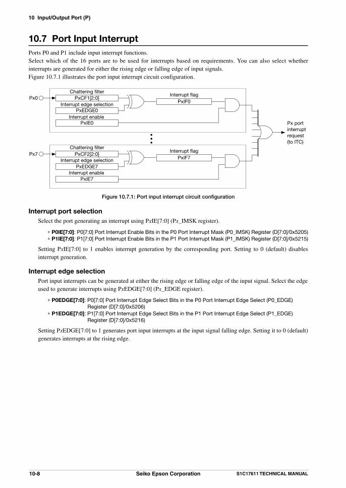
10 Input/Output Port (P)
10-8 Seiko Epson Corporation S1C17611 TECHNICAL MANUAL
10.7 Port Input InterruptPorts P0 and P1 include input interrupt functions.Select which of the 16 ports are to be used for interrupts based on requirements. You can also select whether interrupts are generated for either the rising edge or falling edge of input signals.Figure 10.7.1 illustrates the port input interrupt circuit configuration.
PxCF1[2:0]
PxEDGE0
Interrupt flagPxIF0
PxIE0
PxCF2[2:0]
PxEDGE7
PxIF7
PxIE7
• •
•Interrupt flag
Chattering filter
Interrupt enable
Interrupt edge selectionPx0
Px7
Px port interrupt request (to ITC)
Chattering filter
Interrupt enable
Interrupt edge selection
Figure 10.7.1: Port input interrupt circuit configuration
Interrupt port selection Select the port generating an interrupt using PxIE[7:0] (Px_IMSK register).
* P0IE[7:0]: P0[7:0] Port Interrupt Enable Bits in the P0 Port Interrupt Mask (P0_IMSK) Register (D[7:0]/0x5205)* P1IE[7:0]: P1[7:0] Port Interrupt Enable Bits in the P1 Port Interrupt Mask (P1_IMSK) Register (D[7:0]/0x5215)
Setting PxIE[7:0] to 1 enables interrupt generation by the corresponding port. Setting to 0 (default) disables interrupt generation.
Interrupt edge selection Port input interrupts can be generated at either the rising edge or falling edge of the input signal. Select the edge
used to generate interrupts using PxEDGE[7:0] (Px_EDGE register).
* P0EDGE[7:0]: P0[7:0] Port Interrupt Edge Select Bits in the P0 Port Interrupt Edge Select (P0_EDGE) Register (D[7:0]/0x5206)
* P1EDGE[7:0]: P1[7:0] Port Interrupt Edge Select Bits in the P1 Port Interrupt Edge Select (P1_EDGE) Register (D[7:0]/0x5216)
Setting PxEDGE[7:0] to 1 generates port input interrupts at the input signal falling edge. Setting it to 0 (default) generates interrupts at the rising edge.

10 Input/Output Port (P)
S1C17611 TECHNICAL MANUAL Seiko Epson Corporation 10-9
Interrupt flags The ITC is able to accept interrupt requests for both P0 and P1 port interrupts, and the P port module contains
interrupt flags PxIF[7:0] corresponding to the individual 16 ports to enable individual control of the 16 P0[7:0] and P1[7:0] port interrupts. PxIF[7:0] will be set to 1 at the specified edge (rising or falling edge) of the input signal. A P0 or P1 port interrupt request signal is also output to the ITC at the same time if the corresponding PxIE[7:0] is set to 1. Meeting the ITC and S1C17 core interrupt conditions generates an interrupt.
* P0IF[7:0]: P0[7:0] Port Interrupt Flags in the P0 Port Interrupt Flag (P0_IFLG) Register (D[7:0]/0x5207)* P1IF[7:0]: P1[7:0] Port Interrupt Flags in the P1 Port Interrupt Flag (P1_IFLG) Register (D[7:0]/0x5217)
PxIF[7:0] is reset by writing as 1.
Note: • The P port module interrupt flag PxIF[7:0] must be reset within the interrupt processing routine following a port interrupt to prevent recurring interrupts.
• To prevent generating unnecessary interrupts, reset the relevant PxIF[7:0] before permitting interrupts for the required port using PxIE[7:0] (Px_IMSK register).
Interrupt vector The port interrupt vector numbers and vector addresses are as shown below.
Table 10.7.1: Port interrupt vectorsPort Vector number Vector address
P0 4 (0x04) TTBR + 0x10P1 5 (0x05) TTBR + 0x14
Other interrupt settings The ITC allows the precedence of P0 and P1 port interrupts to be set between level 0 (default) and level 7. The
PSR (S1C17 core internal processor status register) IE (interrupt enable) bit must be set to 1 to generate actual interrupts.
For specific information on interrupt processing, see “6 Interrupt Controller (ITC).”
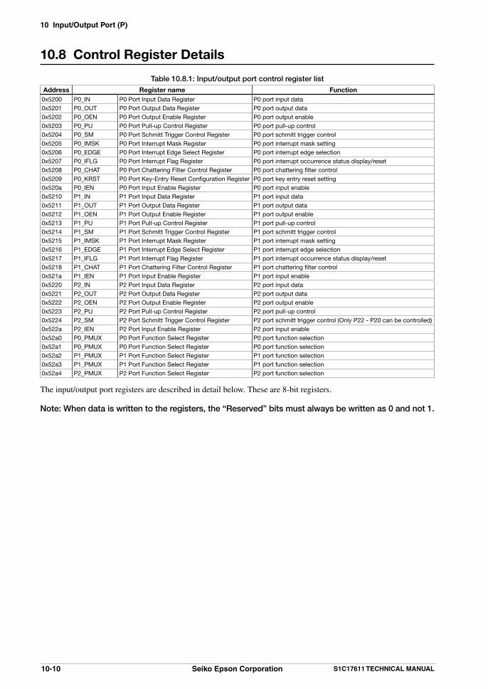
10 Input/Output Port (P)
10-10 Seiko Epson Corporation S1C17611 TECHNICAL MANUAL
10.8 Control Register Details
Table 10.8.1: Input/output port control register listAddress Register name Function
0x5200 P0_IN P0 Port Input Data Register P0 port input data0x5201 P0_OUT P0 Port Output Data Register P0 port output data0x5202 P0_OEN P0 Port Output Enable Register P0 port output enable0x5203 P0_PU P0 Port Pull-up Control Register P0 port pull-up control0x5204 P0_SM P0 Port Schmitt Trigger Control Register P0 port schmitt trigger control0x5205 P0_IMSK P0 Port Interrupt Mask Register P0 port interrupt mask setting0x5206 P0_EDGE P0 Port Interrupt Edge Select Register P0 port interrupt edge selection0x5207 P0_IFLG P0 Port Interrupt Flag Register P0 port interrupt occurrence status display/reset0x5208 P0_CHAT P0 Port Chattering Filter Control Register P0 port chattering filter control0x5209 P0_KRST P0 Port Key-Entry Reset Configuration Register P0 port key entry reset setting0x520a P0_IEN P0 Port Input Enable Register P0 port input enable0x5210 P1_IN P1 Port Input Data Register P1 port input data0x5211 P1_OUT P1 Port Output Data Register P1 port output data0x5212 P1_OEN P1 Port Output Enable Register P1 port output enable0x5213 P1_PU P1 Port Pull-up Control Register P1 port pull-up control0x5214 P1_SM P1 Port Schmitt Trigger Control Register P1 port schmitt trigger control0x5215 P1_IMSK P1 Port Interrupt Mask Register P1 port interrupt mask setting0x5216 P1_EDGE P1 Port Interrupt Edge Select Register P1 port interrupt edge selection0x5217 P1_IFLG P1 Port Interrupt Flag Register P1 port interrupt occurrence status display/reset0x5218 P1_CHAT P1 Port Chattering Filter Control Register P1 port chattering filter control0x521a P1_IEN P1 Port Input Enable Register P1 port input enable0x5220 P2_IN P2 Port Input Data Register P2 port input data0x5221 P2_OUT P2 Port Output Data Register P2 port output data0x5222 P2_OEN P2 Port Output Enable Register P2 port output enable 0x5223 P2_PU P2 Port Pull-up Control Register P2 port pull-up control0x5224 P2_SM P2 Port Schmitt Trigger Control Register P2 port schmitt trigger control (Only P22 - P20 can be controlled)0x522a P2_IEN P2 Port Input Enable Register P2 port input enable0x52a0 P0_PMUX P0 Port Function Select Register P0 port function selection0x52a1 P0_PMUX P0 Port Function Select Register P0 port function selection0x52a2 P1_PMUX P1 Port Function Select Register P1 port function selection0x52a3 P1_PMUX P1 Port Function Select Register P1 port function selection0x52a4 P2_PMUX P2 Port Function Select Register P2 port function selection
The input/output port registers are described in detail below. These are 8-bit registers.
Note: When data is written to the registers, the “Reserved” bits must always be written as 0 and not 1.

10 Input/Output Port (P)
S1C17611 TECHNICAL MANUAL Seiko Epson Corporation 10-11
0x5200/0x5210/0x5220: Px Port Input Data Registers (Px_IN)Register name Address Bit Name Function Setting Init. R/W Remarks
P0 Port Input Data Register(P0_IN)
0x5200(8 bits)
D7–0 P0IN[7:0] P0[7:0] port input data 1 1 (H) 0 0 (L) × R
P1 Port Input Data Register(P1_IN)
0x5210(8 bits)
D7–0 P1IN[7:0] P1[7:0] port input data 1 1 (H) 0 0 (L) × R
P2 Port Input Data Register(P2_IN)
0x5220(8 bits)
D7-3 – reserved – – – 0 when being read.D2–0 P2IN[2:0] P2[2:0] port input data 1 1 (H) 0 0 (L) × R
Note: The “x” in the bit names indicates the port number (0 to 2).
D[7:0] PxIN[7:0]: Px[7:0] Port Input Data Bits Read out the P port pin status. (Default: external pin status) 1(R): High level 0(R): Low level
PxIN[7:0] correspond directly to the Px[7:0] pins and read the pin voltage level regardless of input/output mode. 1 is read when the pin voltage is High; 0 is read when the voltage is Low.
Writing operations to the read-only PxIN[7:0] are disabled.

10 Input/Output Port (P)
10-12 Seiko Epson Corporation S1C17611 TECHNICAL MANUAL
0x5201/0x5211/0x5221: Px Port Output Data Registers (Px_OUT)Register name Address Bit Name Function Setting Init. R/W Remarks
P0 Port Output Data Register(P0_OUT)
0x5201(8 bits)
D7–0 P0OUT[7:0] P0[7:0] port output data 1 1 (H) 0 0 (L) 0 R/W
P1 Port Output Data Register(P1_OUT)
0x5211(8 bits)
D7–0 P1OUT[7:0] P1[7:0] port output data 1 1 (H) 0 0 (L) 0 R/W
P2 Port Output Data Register(P2_OUT)
0x5221(8 bits)
D7-3 – reserved – – – 0 when being read.D2–0 P2OUT[2:0] P2[2:0] port output data 1 1 (H) 0 0 (L) 0 R/W
Note: The “x” in the bit names indicates the port number (0 to 2).
D[7:0] PxOUT[7:0]: Px[7:0] Port Output Data Bits Set the data to be output from the port pin. 1(R/W): High level 0(R/W): Low level (default)
PxOUT[7:0] correspond directly to the Px[7:0] pins and output data from the port pin as written. Setting the data bit to 1 sets the port pin to High; setting it to 0 sets it to Low.
Port data can also be written in input mode.

10 Input/Output Port (P)
S1C17611 TECHNICAL MANUAL Seiko Epson Corporation 10-13
0x5202/0x5212/0x5222: Px Port Output Enable Registers (Px_OEN)Register name Address Bit Name Function Setting Init. R/W Remarks
P0 Port Output Enable Register(P0_OEN)
0x5202(8 bits)
D7–0 P0OEN[7:0] P0[7:0] port output enable select 1 OutputEnable
0 OutputDisable
0 R/W
P1 Port Output Enable Register(P1_OEN)
0x5212(8 bits)
D7–0 P1OEN[7:0] P1[7:0] port output enable select 1 OutputEnable
0 OutputDisable
0 R/W
P2 Port Output Enable Register(P2_OEN)
0x5222(8 bits)
D7-3 – reserved – – – 0 when being read.D2–0 P2OEN[2:0] P2[2:0] port output enable select 1 Output
Enable0 Output
Disable0 R/W
Note: The “x” in the bit names indicates the port number (0 to 2).
D[7:0] PxIOEN[7:0]: Px[7:0] Port Output Enable Select Bits Set Port Output to enable/disable 1(R/W): Enable 0(R/W): Disable (default)
PxOEN[7:0] are the output enable bits corresponding directly to the Px[7:0] ports. Setting to 1 selects output mode, while setting to 0 selects high inpedence. The peripheral module function determines the input/output direction for when a pin is used for peripheral modules.
For the input/output control by each register, refer to “Table 10.3.1 Data Input/Output list.”
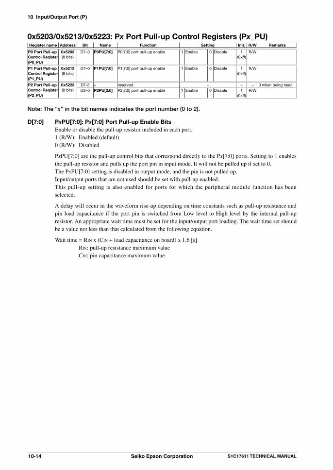
10 Input/Output Port (P)
10-14 Seiko Epson Corporation S1C17611 TECHNICAL MANUAL
0x5203/0x5213/0x5223: Px Port Pull-up Control Registers (Px_PU)Register name Address Bit Name Function Setting Init. R/W Remarks
P0 Port Pull-up Control Register(P0_PU)
0x5203(8 bits)
D7–0 P0PU[7:0] P0[7:0] port pull-up enable 1 Enable 0 Disable 1(0xff)
R/W
P1 Port Pull-up Control Register(P1_PU)
0x5213(8 bits)
D7–0 P1PU[7:0] P1[7:0] port pull-up enable 1 Enable 0 Disable 1(0xff)
R/W
P2 Port Pull-up Control Register(P2_PU)
0x5223(8 bits)
D7-3 – reserved – – – 0 when being read.D2–0 P2PU[2:0] P2[2:0] port pull-up enable 1 Enable 0 Disable 1
(0xff)R/W
Note: The “x” in the bit names indicates the port number (0 to 2).
D[7:0] PxPU[7:0]: Px[7:0] Port Pull-up Enable Bits Enable or disable the pull-up resistor included in each port. 1 (R/W): Enabled (default) 0 (R/W): Disabled
PxPU[7:0] are the pull-up control bits that correspond directly to the Px[7:0] ports. Setting to 1 enables the pull-up resistor and pulls up the port pin in input mode. It will not be pulled up if set to 0.
The PxPU[7:0] setting is disabled in output mode, and the pin is not pulled up. Input/output ports that are not used should be set with pull-up enabled. This pull-up setting is also enabled for ports for which the peripheral module function has been
selected.
A delay will occur in the waveform rise-up depending on time constants such as pull-up resistance and pin load capacitance if the port pin is switched from Low level to High level by the internal pull-up resistor. An appropriate wait time must be set for the input/output port loading. The wait time set should be a value not less than that calculated from the following equation.
Wait time = RIN x (CIN + load capacitance on board) x 1.6 [s] RIN: pull-up resistance maximum value CIN: pin capacitance maximum value

10 Input/Output Port (P)
S1C17611 TECHNICAL MANUAL Seiko Epson Corporation 10-15
0x5204/0x5214/0x5224: Px Port Schmitt Trigger Control Registers (Px_SM)Register name Address Bit Name Function Setting Init. R/W Remarks
P0 Port Schmitt Trigger Control Register(P0_SM)
0x5204(8 bits)
D7–0 P0SM[7:0] P0[7:0] port Schmitt trigger input enable
1 Enable(Schmitt)
0 Disable(CMOS)
1(0xff)
R/W
P1 Port Schmitt Trigger Control Register(P1_SM)
0x5214(8 bits)
D7–0 P1SM[7:0] P1[7:0] port Schmitt trigger input enable
1 Enable(Schmitt)
0 Disable(CMOS)
1(0xff)
R/W
P2 Port Schmitt Trigger Control Register(P2_SM)
0x5224(8 bits)
D7–3 – reserved – – – 1 when being read.D2–0 P2SM[2:0] P2[2:0] port Schmitt trigger input
enable1 Enable
(Schmitt)0 Disable
(CMOS)1
(0xff)R/W
Note: The “x” in bit names indicates the port number (0 or 1).
D[7:0] PxSM[7:0]: Px[7:0] Port Schmitt Trigger Input Enable Bits (P2 port is P2SM[2:0]) Enable or disable the Schmitt trigger input buffer for each port. 1(R/W): Enable (Schmitt input) (default) 0(R/W): Disable (CMOS level)
PxSM[7:0] are Schmitt input control bits that correspond directly to the Px[7:0] ports. Setting to 1 enables the Schmitt input buffer, and setting to 0 uses the CMOS level input buffer.
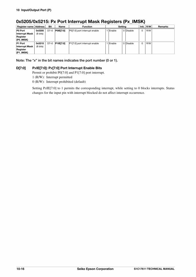
10 Input/Output Port (P)
10-16 Seiko Epson Corporation S1C17611 TECHNICAL MANUAL
0x5205/0x5215: Px Port Interrupt Mask Registers (Px_IMSK)Register name Address Bit Name Function Setting Init. R/W Remarks
P0 Port Interrupt Mask Register(P0_IMSK)
0x5205(8 bits)
D7–0 P0IE[7:0] P0[7:0] port interrupt enable 1 Enable 0 Disable 0 R/W
P1 Port Interrupt Mask Register(P1_IMSK)
0x5215(8 bits)
D7–0 P1IE[7:0] P1[7:0] port interrupt enable 1 Enable 0 Disable 0 R/W
Note: The “x” in the bit names indicates the port number (0 or 1).
D[7:0] PxIE[7:0]: Px[7:0] Port Interrupt Enable Bits Permit or prohibit P0[7:0] and P1[7:0] port interrupt. 1 (R/W): Interrupt permitted 0 (R/W): Interrupt prohibited (default)
Setting PxIE[7:0] to 1 permits the corresponding interrupt, while setting to 0 blocks interrupts. Status changes for the input pin with interrupt blocked do not affect interrupt occurrence.

10 Input/Output Port (P)
S1C17611 TECHNICAL MANUAL Seiko Epson Corporation 10-17
0x5206/0x5216: Px Port Interrupt Edge Select Registers (Px_EDGE)Register name Address Bit Name Function Setting Init. R/W Remarks
P0 Port Interrupt Edge Select Register(P0_EDGE)
0x5206(8 bits)
D7–0 P0EDGE[7:0] P0[7:0] port interrupt edge select 1 Falling edge 0 Rising edge 0 R/W
P1 Port Interrupt Edge Select Register(P1_EDGE)
0x5216(8 bits)
D7–0 P1EDGE[7:0] P1[7:0] port interrupt edge select 1 Falling edge 0 Rising edge 0 R/W
Note: The “x” in the bit names indicates the port number (0 or 1).
D[7:0] PxEDGE[7:0]: Px[7:0] Port Interrupt Edge Select Bits Select the input signal edge for generating P0[7:0] and P1[7:0] port interrupts. 1 (R/W): Falling edge 0 (R/W): Rising edge (default)
Port interrupts are generated at the input signal falling edge if PxEDGE[7:0] are set to 1 and at the rising edge if set to 0.

10 Input/Output Port (P)
10-18 Seiko Epson Corporation S1C17611 TECHNICAL MANUAL
0x5207/0x5217: Px Port Interrupt Flag Registers (Px_IFLG)Register name Address Bit Name Function Setting Init. R/W Remarks
P0 Port Interrupt Flag Register(P0_IFLG)
0x5207(8 bits)
D7–0 P0IF[7:0] P0[7:0] port interrupt flag 1 Cause of interrupt occurred
0 Cause of interrupt not occurred
0 R/W Reset by writing 1.
P1 Port Interrupt Flag Register(P1_IFLG)
0x5217(8 bits)
D7–0 P1IF[7:0] P1[7:0] port interrupt flag 1 Cause of interrupt occurred
0 Cause of interrupt not occurred
0 R/W Reset by writing 1.
Note: The “x” in the bit names indicates the port number (0 or 1).
D[7:0] PxIF[7:0]: Px[7:0] Port Interrupt Flags These are interrupt flags indicating the interrupt factor occurrence status. 1(R): Interrupt factor present 0(R): No interrupt factor (default) 1(W): Reset flag 0(W): Disabled
PxIF[7:0] are interrupt flags corresponding to the individual 16 ports of P0[7:0] and P1[7:0]. PxIF[7:0] will be set to 1 at the specified edge (rising or falling edge) of the input signal. A P0 or P1 port interrupt request signal is also output to the ITC at the same time if the corresponding PxIE[7:0] (Px_IMSK register) is set to 1. This interrupt request signal causes the P0/P1 port interrupt flag inside the ITC to be set to 1. Meeting the ITC and S1C17 core interrupt conditions generates an interrupt.
PxIF[7:0] is reset by writing as 1.
Note: • The P port module interrupt flag PxIF[7:0] must be reset within the interrupt processing routine following a port interrupt to prevent recurring interrupts.
• To prevent genarating unnecessary interrupts, reset the relevant PxIF[7:0] before permitting interrupts for the required port using PxIE[7:0] (Px_IMSK register).
* P0IE[7:0]: P0[7:0] Port Interrupt Enable Bits in the P0 Port Interrupt Mask (P0_IMSK) Register (D[7:0]/0x5205)
* P1IE[7:0]: P1[7:0] Port Interrupt Enable Bits in the P1 Port Interrupt Mask (P1_IMSK) Register (D[7:0]/0x5215)

10 Input/Output Port (P)
S1C17611 TECHNICAL MANUAL Seiko Epson Corporation 10-19
0x5208/0x5218: Px Port Chattering Filter Control Registers (Px_CHAT)Register name Address Bit Name Function Setting Init. R/W Remarks
P0 Port Chattering Filter Control Register(P0_CHAT)
0x5208(8 bits)
D7 – reserved – – – 0 when being read.D6–4 P0CF2[2:0] P0[7:4] chattering filter time select P0CF2[2:0] Filter time 0 R/W
0x70x60x50x40x30x20x10x0
16384/fPCLK
8192/fPCLK
4096/fPCLK
2048/fPCLK
1024/fPCLK
512/fPCLK
256/fPCLK
None
0x0 R/W
D3 – reserved – – – 0 when being read.D2–0 P0CF1[2:0] P0[3:0] chattering filter time select P0CF1[2:0] Filter time 0x0 R/W
0x70x60x50x40x30x20x10x0
16384/fPCLK
8192/fPCLK
4096/fPCLK
2048/fPCLK
1024/fPCLK
512/fPCLK
256/fPCLK
None
P1 Port Chattering Filter Control Register(P1_CHAT)
0x5218(8 bits)
D7 – reserved – – – 0 when being read.D6–4 P1CF2[2:0] P1[7:4] chattering filter time select P0CF2[2:0] Filter time 0 R/W
0x70x60x50x40x30x20x10x0
16384/fPCLK
8192/fPCLK
4096/fPCLK
2048/fPCLK
1024/fPCLK
512/fPCLK
256/fPCLK
None
0x0 R/W
D3 – reserved – – – 0 when being read.D2–0 P1CF1[2:0] P1[3:0] chattering filter time select P0CF1[2:0] Filter time 0x0 R/W
0x70x60x50x40x30x20x10x0
16384/fPCLK
8192/fPCLK
4096/fPCLK
2048/fPCLK
1024/fPCLK
512/fPCLK
256/fPCLK
None
Note: The “x” in the bit names indicates the port number (0 or 1).
D7 Reserved
D[6:4] PxCF2[2:0]: Px[7:4] Chattering Filter Time Select Bits Set the chattering filter circuit included in the P0[7:4] port.
D3 Reserved
D[2:0] PxCF1[2:0]: Px[3:0] Chattering Filter Time Select Bits Set the chattering filter circuit included in the P0[3:0] port. The P0 or P1 port includes a chattering filter circuit for key entry or port interrupt. You can select
whether to use this function respectively for P0[3:0], P0[7:4], P1[3:0] and P1[7:4] ports using PxCF1/2[2:0]. You can also select relevant verification time accordingly.
Table 10.8.2: Chattering filter function settings
P0CFx[2:0] Verification time *
0x7 16384/fPCLK (8ms)0x6 8192/fPCLK (4ms)0x5 4096/fPCLK (2ms)0x4 2048/fPCLK (1ms)0x3 1024/fPCLK (512µs)0x2 512/fPCLK (256µs)0x1 256/fPCLK (128µs)0x0 No verification time (Off)
(Default: 0x0, *when OSC3 = 2 MHz and PCLK = OSC3)
10 Input/Output Port (P)
10-20 Seiko Epson Corporation S1C17611 TECHNICAL MANUAL
Note: • The chattering filter verification time refers to the maximum pulse width that can be filtered. Generating an input interrupt requires a minimum input time of the verification time and a maximum input time of twice the verification time.
• P0/P1 port interrupts must be blocked when Px_CHAT register settings are being changed. Changing the setting while interrupts are permitted may generate inadvertent P0/P1 interrupts. Twice of the verification time is required at the maximum until the chattering filter circuit becomes stable. Interrupts must be allowed only after this time for stabilization has passed.
• A phenomenon may occur in which the internal signal oscillates due to the time elapsed until the signal reaches the threshold value if the input signal rise-up/drop-off time is delayed. Since input interrupts will malfunction under these conditions, the input signal rise-up/drop-off time should normally be set to 25 ns or less.
• An unexpected interrupt may occur after SLEEP status is canceled if the slp instruction is executed while the chattering filter function is enabled. The chattering filter must be disabled before placing the CPU into SLEEP status.

10 Input/Output Port (P)
S1C17611 TECHNICAL MANUAL Seiko Epson Corporation 10-21
0x5209: P0 Port Key-Entry Reset Configuration Register (P0_KRST)Register name Address Bit Name Function Setting Init. R/W Remarks
P0 Port Key-Entry Reset Configuration Register(P0_KRST)
0x5209(8 bits)
D7–2 – reserved – – – 0 when being read.D1–0 P0KRST[1:0] P0 port key-entry reset
configurationP0KRST[1:0] Configuration 0x0 R/W
0x30x20x10x0
P0[5:2] = 0P0[4:2] = 0P0[3:2] = 0
Disable
D[7:2] Reserved
D[1:0] P0KRST[1:0]: P0 Port Key-Entry Reset Configuration Bits Select the port combination used for P0 port key entry resetting.
Table 10.8.3: P0 port key entry input reset settings
P0KRST[1:0] Ports used0x3 P02, P03, P04, P050x2 P02, P03, P040x1 P02, P030x0 Not used
(Default: 0x0)
The key entry reset function performs an initial reset by inputting Low level simultaneously from externally to the port selected here.
For example, if P0KRST[1:0] is set to 0x3, an initial reset is performed when the four ports P02 to P05 are simultaneously set to Low level.
Set P0KRST[1:0] to 0x0 when this reset function is not used.
Note: • Make sure the specified ports are not simultaneously switched to Low during normal operations when using the P0 port key-entry reset function.
• The P0 port key entry reset function is disabled on initial resetting and cannot be used for resetting at power-on.

10 Input/Output Port (P)
10-22 Seiko Epson Corporation S1C17611 TECHNICAL MANUAL
0x520a/0x521a/0x522a: Px Port Input Enable Registers (Px_IEN)Register name Address Bit Name Function Setting Init. R/W Remarks
P0 Port Input Enable Register(P0_IEN)
0x520a(8 bits)
D7–0 P0IEN[7:0] P0[7:0] port input enable 1 Enable 0 Disable 0xff R/W
P1 Port Input Enable Register(P1_IEN)
0x521a(8 bits)
D7–0 P1IEN[7:0] P1[7:0] port input enable 1 Enable 0 Disable 0xff R/W
P2 Port Input Enable Register(P2_IEN)
0x522a(8 bits)
D7-3 – reserved – – – 0 when being read.D2-0 P2IEN[2:0] P2[2:0] port input enable 1 Enable 0 Disable 0xff R/W
Note: The “x” in the bit names indicates the port number (0 to 4).
D[7:0] PxIEN[7:0]: Px[7:0] Port Input Enable Bits Permits or prevents port input. 1(R/W): Permit (default) 0(R/W): Prohibit
PxIEN[7:0] are input enable bits that correspond directly to the Px[7:0] ports. Setting to 1 enables the input signal level to be read from the Px_IN register, while setting to 0 prevents signal input and fixes the input data values read out to 0.
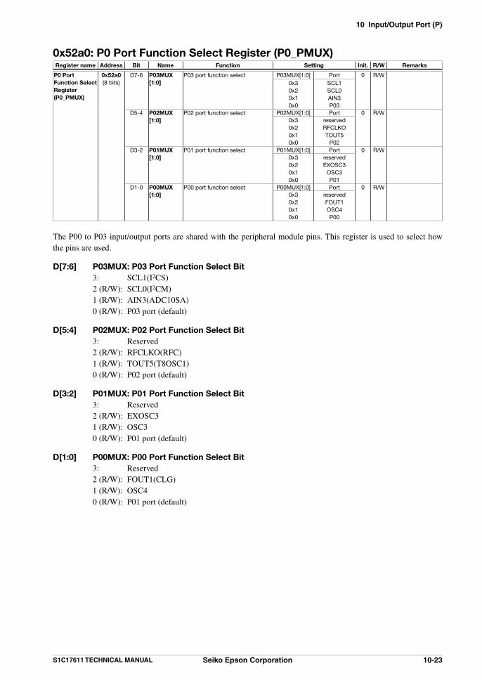
10 Input/Output Port (P)
S1C17611 TECHNICAL MANUAL Seiko Epson Corporation 10-23
0x52a0: P0 Port Function Select Register (P0_PMUX)Register name Address Bit Name Function Setting Init. R/W Remarks
P0 Port Function Select Register(P0_PMUX)
0x52a0(8 bits)
D7-6 P03MUX[1:0]
P03 port function select P03MUX[1:0] Port 0 R/W0x30x20x10x0
SCL1SCL0AIN3P03
D5-4 P02MUX[1:0]
P02 port function select P02MUX[1:0] Port 0 R/W0x30x20x10x0
reservedRFCLKOTOUT5
P02D3-2 P01MUX
[1:0]P01 port function select P01MUX[1:0] Port 0 R/W
0x30x20x10x0
reservedEXOSC3
OSC3P01
D1-0 P00MUX[1:0]
P00 port function select P00MUX[1:0] Port 0 R/W0x30x20x10x0
reservedFOUT1OSC4P00
The P00 to P03 input/output ports are shared with the peripheral module pins. This register is used to select how the pins are used.
D[7:6] P03MUX: P03 Port Function Select Bit 3: SCL1(I2CS) 2 (R/W): SCL0(I2CM) 1 (R/W): AIN3(ADC10SA) 0 (R/W): P03 port (default)
D[5:4] P02MUX: P02 Port Function Select Bit 3: Reserved 2 (R/W): RFCLKO(RFC) 1 (R/W): TOUT5(T8OSC1) 0 (R/W): P02 port (default)
D[3:2] P01MUX: P01 Port Function Select Bit 3: Reserved 2 (R/W): EXOSC3 1 (R/W): OSC3 0 (R/W): P01 port (default)
D[1:0] P00MUX: P00 Port Function Select Bit 3: Reserved 2 (R/W): FOUT1(CLG) 1 (R/W): OSC4 0 (R/W): P01 port (default)

10 Input/Output Port (P)
10-24 Seiko Epson Corporation S1C17611 TECHNICAL MANUAL
0x52a1: P0 Port Function Select Register (P0_PMUX)Register name Address Bit Name Function Setting Init. R/W Remarks
P0 Port Function Select Register(P0_PMUX)
0x52a1(8 bits)
D7-6 P07MUX[1:0]
P07 port function select P07MUX[1:0] Port 0 R/W0x30x20x10x0
reservedFOUTH
RFINP07
D5-4 P06MUX[1:0]
P06 port function select P06MUX[1:0] Port 0 R/W0x30x20x10x0
LFROFOUT1AIN0P06
D3-2 P05MUX[1:0]
P05 port function select P05MUX[1:0] Port 0 R/W0x30x20x10x0
reservedTOUT4AIN1
P05/EXCL3 (T16E)
D1-0 P04MUX[1:0]
P04 port function select P04MUX[1:0] Port 0 R/W0x30x20x10x0
SDA1SDA0AIN2P04
The P04 to P07 input/output ports are shared with the peripheral module pins. This register is used to select how the pins are used.
D[7:6] P07MUX: P07 Port Function Select Bit 3: Reserved 2 (R/W): FOUTH(CLG) 1 (R/W): RFIN(RFC) 0 (R/W): P07 (default)
D[5:4] P06MUX: P06 Port Function Select Bit 3: LFRO(LCD) 2 (R/W): FOUT1(CLG) 1 (R/W): AIN0(ADC10SA) 0 (R/W): P06 (default)
D[3:2] P05MUX: P05 Port Function Select Bit 3: Reserved 2 (R/W): TOUT4(T16E) 1 (R/W): AIN1(ADC10SA) 0 (R/W): P05/EXCL3(T16E) (default)
*To use the P05 pin as EXCL3 input, PxOEN register must be set to 0 and PxIEN must be set to 1.
D[1:0] P04MUX: P04 Port Function Select Bit 3: SDA1(I2CS) 2 (R/W): SDA0(I2CM) 1 (R/W): AIN2(ADC10SA) 0 (R/W): P04 (default)

10 Input/Output Port (P)
S1C17611 TECHNICAL MANUAL Seiko Epson Corporation 10-25
0x52a2: P1 Port Function Select Register (P1_PMUX)Register name Address Bit Name Function Setting Init. R/W Remarks
P1 Port Function Select Register(P1_PMUX)
0x52a2(8 bits)
D7-6 P13MUX[1:0]
P13 port function select P13MUX[1:0] Port 0 R/W0x30x20x10x0
TOUTN3FOUTHSOUTP13
D5-4 P12MUX[1:0]
P12 port function select P12MUX[1:0] Port 0 R/W0x30x20x10x0
TOUT3SCLKSENBP12
D3-2 P11MUX[1:0]
P11 port function select P11MUX[1:0] Port 0 R/W0x30x20x10x0
reservedTOUT4SENAP11
D1-0 P10MUX[1:0]
P10 port function select P10MUX[1:0] Port 0 R/W0x30x20x10x0
reservedTOUTN4
REFP10
The P10 to P13 input/output ports are shared with the peripheral module pins. This register is used to select how the pins are used.
D[7:6] P13MUX: P13 Port Function Select Bit 3: TOUTN3(T16E) 2 (R/W): FOUTH(CLG) 1 (R/W): SOUT(UART) 0 (R/W): P13 (default)
D[5:4] P12MUX: P12 Port Function Select Bit 3: TOUT3(T16E) 2 (R/W): SCLK(UART) 1 (R/W): SENB(RFC) 0 (R/W): P12 (default)
D[3:2] P11MUX: P11 Port Function Select Bit 3: Reserved 2 (R/W): TOUT4(T16E) 1 (R/W): SENA(RFC) 0 (R/W): P11 (default)
D[1:0] P10MUX: P10 Port Function Select Bit 3: Reserved 2 (R/W): TOUTN4(T16E) 1 (R/W): REF(RFC) 0 (R/W): P10 (default)

10 Input/Output Port (P)
10-26 Seiko Epson Corporation S1C17611 TECHNICAL MANUAL
0x52a3: P1 Port Function Select Register (P1_PMUX)Register name Address Bit Name Function Setting Init. R/W Remarks
P1 Port Function Select Register(P1_PMUX)
0x52a3(8 bits)
D7 – reserved – – – 0 when being read.D6 P17MUX P17 port function select P17MUX[1:0] Port 0 R/W
0x10x0
SDOP17/EXCL1
D5 – reserved – – – 0 when being read.D4 P16MUX P16 port function select P16MUX[1:0] Port 0 R/W
0x10x0
SDIP16/EXCL2
D3-2 P15MUX[1:0]
P15 port function select P15MUX[1:0] Port 0 R/W0x30x20x10x0
TOUT3#BFR
#SPISSP15
D1-0 P14MUX[1:0]
P14 port function select P14MUX[1:0] Port 0 R/W0x30x20x10x0
reserved#ADTRG
SINP14/EXCL4
The P14 to P17 input/output ports are shared with the peripheral module pins. This register is used to select how the pins are used.
D7 Reserved
D6 P17MUX: P17 Port Function Select Bit 1 (R/W): SDO(SPI) 0 (R/W): P17/EXCL1(T16) (default)
*To use the P17 pin as EXCL1 input, PxOEN register must be set to 0 and PxIEN must be set to 1.
D5 Reserved
D4 P16MUX: P16 Port Function Select Bit 1 (R/W): SDI(SPI) 0 (R/W): P16/EXCL2(T16) (default)
*To use the P16 pin as EXCL2 input, PxOEN register must be set to 0 and PxIEN must be set to 1.
D[3:2] P15MUX: P15 Port Function Select Bit 3 (R/W): TOUT3(T16E) 2 (R/W): #BFR(I2CS) 1 (R/W): #SPISS(SPI) 0 (R/W): P15 (default)
D[1:0] P14MUX[1:0]: P14 Port Function Select Bit 3 (R/W): Reserved 2 (R/W): #ADTRG(ADC10SA) 1 (R/W): SIN(UART) 0 (R/W): P14/EXCL4(T16E) (default)
*To use the P14 pin as EXCL4 input, PxOEN register must be set to 0 and PxIEN must be set to 1.

10 Input/Output Port (P)
S1C17611 TECHNICAL MANUAL Seiko Epson Corporation 10-27
0x52a4: P2 Port Function Select Register (P2_PMUX)Register name Address Bit Name Function Setting Init. R/W Remarks
P2 Port Function Select Register(P2_PMUX)
0x52a4(8 bits)
D7 – reserved – – – 0 when being read.D6 P23MUX P23 port function select P23MUX[1:0] Port 0 R/W
0x10x0
reservedDCLK
D5 – reserved – – – 0 when being read.D4 P22MUX P22 port function select P22MUX[1:0] Port 0 R/W
0x10x0
P22DST2
D3 – reserved – – – 0 when being read.D2 P21MUX P21 port function select P21MUX[1:0] Port 0 R/W
0x10x0
P21DSIO
D1-0 P20MUX[1:0]
P20 port function select P20MUX[1:0] Port 0 R/W0x30x20x10x0
reservedTOUT5SPICLK
P20/EXCL0
The P20 to P23 input/output ports are shared with the peripheral module pins. This register is used to select how the pins are used.
D[7:6] P23MUX: P23 Port Function Select Bit 3 (R/W): Reserved 2 (R/W): Reserved 1 (R/W): Reserved 0 (R/W): DCLK(DBG) (default)
D[5:4] P22MUX: P22 Port Function Select Bit 3 (R/W): Reserved 2 (R/W): Reserved 1 (R/W): P22 0 (R/W): DST2(DBG) (default)
D[3:2] P21MUX: P21 Port Function Select Bit 3 (R/W): Reserved 2 (R/W): Reserved 1 (R/W): P21 0 (R/W): DSIO(DBG) (default)
D[1:0] P20MUX: P20 Port Function Select Bit 3 (R/W): Reserved 2 (R/W): TOUT5(T8OSC1) 1 (R/W): SPICLK(SPI) 0 (R/W): P20/EXCL0(T16) (default)
*To use the P20 pin as EXCL0 input, PxOEN register must be set to 0 and PxIEN must be set to 1.

10 Input/Output Port (P)
10-28 Seiko Epson Corporation S1C17611 TECHNICAL MANUAL
10.9 Precautions
Operation clock• The PCLK clock must be fed from the clock generator to access the input/output port. The prescaler output clock is also needed to operate the P0 port chattering filter. Switch on the prescaler
when using this function.
Pull-up• A delay will occur in the waveform rise-up depending on time constants such as pull-up resistance and pin
load capacitance if the port pin is switched from Low level to High level by the internal pull-up resistor. An appropriate wait time must be set for the input/output port loading. The wait time set should be a value not less than that calculated from the following equation.
Wait time = RIN x (CIN + load capacitance on board) x 1.6 [s] RIN: pull-up resistance maximum value CIN: pin capacitance maximum value
• Input/output ports that are not used should be set with pull-up resistance enabled.
P0 and P1 port interrupts• Reset the corresponding interrupt flags P0IF[7:0] (0x5207) and P1IF[7:0] (0x5217) within the interrupt
processing routine following a port interrupt to prevent recurring interrupts.
• To prevent generating unnecessary interrupts, reset the corresponding interrupt flag—P0IF[7:0] (0x5207) or P1IF[7:0] (0x5217)—before permitting interrupts for the required port with the P0_IMSK register (0x5205) or P1_IMSK register (0x5215).
P0/P1 Port chattering filter circuit• P0/P1 port interrupts must be blocked when Px_CHAT register (0x5208/0x5218) settings are being changed.
Changing the setting while interrupts are permitted may generate inadvertent P0/P1 interrupts. Twice of the verification time is required at the maximum until the chattering filter circuit becomes stable. Interrupts must be allowed only after this time for stabilization has passed.
• The chattering filter verification time refers to the maximum pulse width that can be filtered. Generating an input interrupt requires a minimum input time of the verification time and a maximum input time of twice the verification time.
• A phenomenon may occur in which the internal signal oscillates due to the time elapsed until the signal reaches the threshold value if the input signal rise-up/drop-off time is delayed. Since input interrupts will malfunction under these conditions, the input signal rise-up/drop-off time should normally be set to 25 ns or less.
• An unexpected interrupt may occur after SLEEP status is canceled if the slp instruction is executed while the chattering filter function is enabled. The chattering filter must be disabled before placing the CPU into SLEEP status.
P0 port key-entry reset• Make sure the specified ports are not simultaneously switched to Low during normal operations when using
the P0 port key-entry reset function.
• The P0 port key entry reset function is disabled on initial resetting and cannot be used for resetting at power-on.
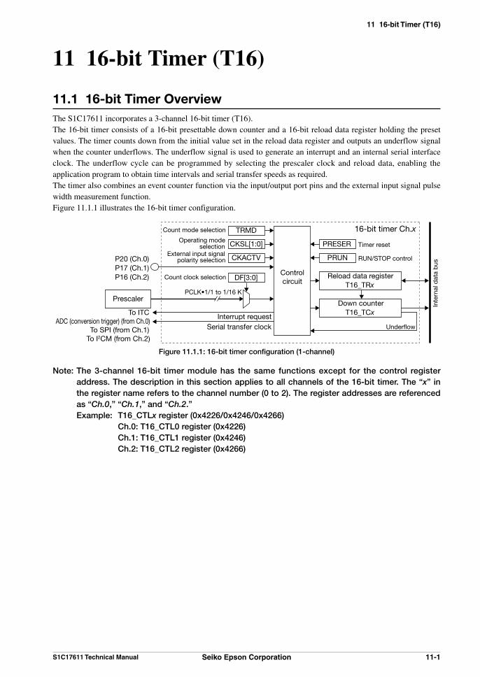
11 16-bit Timer (T16)
S1C17611 Technical Manual Seiko Epson Corporation 11-1
11 16-bit Timer (T16)
11.1 16-bit Timer OverviewThe S1C17611 incorporates a 3-channel 16-bit timer (T16).The 16-bit timer consists of a 16-bit presettable down counter and a 16-bit reload data register holding the preset values. The timer counts down from the initial value set in the reload data register and outputs an underflow signal when the counter underflows. The underflow signal is used to generate an interrupt and an internal serial interface clock. The underflow cycle can be programmed by selecting the prescaler clock and reload data, enabling the application program to obtain time intervals and serial transfer speeds as required.The timer also combines an event counter function via the input/output port pins and the external input signal pulse width measurement function.Figure 11.1.1 illustrates the 16-bit timer configuration.
Reload data registerT16_TRx
PRUN
DF[3:0]
PRESER
Down counterT16_TCx
CKACTV
CKSL[1:0]
TRMD
Prescaler
Controlcircuit
PCLK•1/1 to 1/16 K
Underflow
RUN/STOP control
Count clock selection
Interrupt requestSerial transfer clock
P20 (Ch.0)P17 (Ch.1)P16 (Ch.2)
Timer resetExternal input signal
polarity selection
Operating modeselection
Count mode selection
Inte
rnal
dat
a b
us
16-bit timer Ch.x
To ITCADC (conversion trigger) (from Ch.0)
To SPI (from Ch.1)To I2CM (from Ch.2)
Figure 11.1.1: 16-bit timer configuration (1-channel)
Note: The 3-channel 16-bit timer module has the same functions except for the control register address. The description in this section applies to all channels of the 16-bit timer. The “x” in the register name refers to the channel number (0 to 2). The register addresses are referenced as “Ch.0,” “Ch.1,” and “Ch.2.”
Example: T16_CTLx register (0x4226/0x4246/0x4266) Ch.0: T16_CTL0 register (0x4226) Ch.1: T16_CTL1 register (0x4246) Ch.2: T16_CTL2 register (0x4266)

11 16-bit Timer (T16)
11-2 Seiko Epson Corporation S1C17611 Technical Manual
11.2 16-bit Timer Operating ModesThe 16-bit timer has the following three operating modes:1. Internal clock mode (Normal timer counting internal clock)2. External clock mode (Functions as event counter)3. Pulse width measurement mode (Counts external input pulse width using internal clock)
The operating mode is selected using CKSL[1:0] (D[9:8]/T16_CTLx register).
* CKSL[1:0]: Input Clock and Pulse Width Count Mode Select Bits in the 16-bit Timer Ch.x Control (T16_CTLx) Register (D[9:8]/0x4226/0x4246/0x4266)
Table 11.2.1: Operating mode selection
CKSL[1:0] Operating mode0x3 Reserved0x2 Pulse width measurement mode0x1 External clock mode0x0 Internal clock mode
(Default: 0x0)
11.2.1 Internal Clock Mode
Internal clock mode uses the prescaler output clock as the count clock.The timer counts down from the initial value set in the reload data register and outputs an underflow signal when the counter underflows. The underflow signal is used to generate an interrupt and an internal serial interface clock. The time until underflow occurs can be finely programmed by selecting the prescaler clock and initial counter value, making it useful for serial transfer clock generation and sporadic time measurement.
Count clock selection The count clock is selected by the DF[3:0] (D[3:0]/T16_CLKx register) from the 15 types generated by the
prescaler dividing the PCLK clock into 1/1 to 1/16 K divisions.
* DF[3:0]: Timer Input Clock Select Bits in the 16-bit Timer Ch.x Input Clock Select (T16_CLKx) Register (D[3:0]/0x4220/0x4240/0x4260)
Table 11.2.1.1: Count clock selection
DF[3:0] Prescaler output clock DF[3:0] Prescaler output clock0xf Reserved 0x7 PCLK•1/1280xe PCLK•1/16384 0x6 PCLK•1/640xd PCLK•1/8192 0x5 PCLK•1/320xc PCLK•1/4096 0x4 PCLK•1/160xb PCLK•1/2048 0x3 PCLK•1/80xa PCLK•1/1024 0x2 PCLK•1/40x9 PCLK•1/512 0x1 PCLK•1/20x8 PCLK•1/256 0x0 PCLK•1/1
(Default: 0x0)
Note: • The prescaler must run before operating the 16-bit timer in internal clock mode.
• Make sure the 16-bit timer count is halted before changing count clock settings.
For detailed information on the prescaler control, see “9 Prescaler (PSC).”

11 16-bit Timer (T16)
S1C17611 Technical Manual Seiko Epson Corporation 11-3
11.2.2 External Clock Mode
External clock mode uses the clock and pulses input via the input/output port as a count clock. These inputs can also be used as an event counter. Timer operations other than the input clock are the same as for internal clock mode.
External clock input port The following input ports are used for external clock or pulse input.
Table 11.2.2.1: External clock input port
Timer channel Input signal name Input/output port pinCh.0 EXCL0 P20Ch.1 EXCL1 P17Ch.2 EXCL2 P16
Confirm that the input/output ports used for external clock or pulse input are set to input mode (the default setting). No pin function selection is needed. While the input/output ports function as general purpose inputs, the input signal is also sent to the 16-bit timer.
The P20, P17, and P16 ports used by 16-bit timer Ch.0, Ch.1 and Ch.2 incorporate chattering filter circuits and can also be used as EXCLx inputs. For instructions on controlling chattering filter circuits, see “10.6 P0 and P1 Port Chattering Filter Function.”
For the input rules of external clock, see “28 Electrical Characteristics”.
Signal polarity selection CKACTV (D10/T16_CTLx register) is used in this mode to select the falling edge or rising edge of the input
signal for counting.
* CKACTV: External Clock Active Level Select Bit in the 16-bit Timer Ch.x Control (T16_CTLx) Register (D10/0x4226/0x4246/0x4266)
Counting down uses the rising edge when CKACTV is 1 (default) and uses the falling edge when set to 0.
External input clock
PRUN
Counter (CKACTV = 1)
Counter (CKACTV = 0)
n-1 n-2 n-3 n-4 n-5 n-6 n-7 n-8 n-9 n-10n
n-1 n-2 n-3 n-4 n-5 n-6 n-7 n-8 n-9 n-10n
Figure 11.2.2.1: External clock mode count
The 16-bit timer does not use the prescaler in this mode. If no other peripheral modules use the prescaler clock, the prescaler can be stopped to reduce current consumption. (The prescaler clock is used for P0, P1 port chattering filtering.)

11 16-bit Timer (T16)
11-4 Seiko Epson Corporation S1C17611 Technical Manual
11.2.3 Pulse Width Measurement Mode
In pulse width measurement mode, when pulses with the specified polarity are input from the external clock port, the internal clock is fed only while the signal is active, enabling counting. This enables interrupt generation and input pulse width measurements for pulse inputs of the specified width or greater.
Pulse input port The Input/output port used for external pulse input is the same as for external clock mode (see Table 11.2.2.1).
Input pulses using the input/output port corresponding to the timer channel in input mode.
Count clock selection Counting uses the prescaler output clock selected by DF[3:0] (D[3:0]/T16_CLKx register) in the same way as
for internal clock mode. Select the clock to suit approximate input pulse widths and counting accuracy (see Table 11.2.1.1).
Signal polarity selection CKACTV (D10/T16_CTLx register) is used to select the active level for the pulses counted. The High period is
measured when CKACTV is 1 (default) and the Low period is measured when CKACTV is set to 0.
Internal count clock
PRUN
External input signal
Counter (CKACTV = 0) n-1 n-2 n-3 0x2 0x1 0x0 nn
Internal count clock
PRUN
External input signal
Counter (CKACTV = 1)
Underflow interrupt
0xff 0xfe 0xfd n+3 n+2 n+1 n0x0
Example 1: Pulse width measurement
Example 2: Detecting pulses over specified width
Figure 11.2.3.1: Pulse width measurement mode count operation

11 16-bit Timer (T16)
S1C17611 Technical Manual Seiko Epson Corporation 11-5
11.3 Count ModeThe 16-bit timer features two count modes: Repeat mode and One-shot mode. These modes are selected using the TRMD (D4/T16_CTLx register).
* TRMD: Count Mode Select Bit in the 16-bit Timer Ch.x Control (T16_CTLx) Register (D4/0x4226/0x4246/0x4266)
Repeat mode (TRMD = 0, default) Setting TRMD to 0 sets the 16-bit timer to Repeat mode. In this mode, once the count starts, the 16-bit timer continues running until stopped by the application program.
If the counter underflows, the timer presets the reload data register value into the counter and continues the count. Thus, the timer periodically outputs an underflow pulse. The 16-bit timer should be set to this mode to generate periodic interrupts at desired intervals or to generate a serial transfer clock.
One-shot mode (TRMD = 1) Setting TRMD to 1 sets the 16-bit timer to One-shot mode. In this mode, the 16-bit timer stops automatically as soon as the counter underflows. This means only one
interrupt can be generated after the timer starts. Note that the timer presets the reload data register value to the counter, then stops after an underflow has occurred. The 16-bit timer should be set to this mode to set a specific wait time or for pulse width measurement.

11 16-bit Timer (T16)
11-6 Seiko Epson Corporation S1C17611 Technical Manual
11.4 16-bit Timer Reload Register and Underflow CycleThe reload data register T16_TRx (0x4222/0x4242/0x4262) is used to set the initial value for the down counter.The initial counter value set in the reload data register is preset to the down counter if the 16-bit timer is reset or the counter underflows. If the 16-bit timer is started after resetting, the timer counts down from the reload value (initial value). This means this reload value and the input clock frequency. determines the time elapsed from the point at which the timer starts until the underflow occurs (or between underflows). The time determined is used to obtain the specified wait time, the intervals between periodic interrupts, and the programmable serial interface transfer clock.
One-shot mode
Counter
Repeat mode
Counter
01n-1n n
Preset by timer reset
Preset by timer reset
Auto preset
Underflow
Auto preset
(n = reload data)
01n-1n n
Underflow
Timer start
Timer start
Auto preset
01n-1 n
Underflow
Figure 11.4.1: Preset timing
The underflow cycle can be calculated as follows:
TR + 1 clk_inUnderflow interval = ——— [s] Underflow cycle = ——— [Hz]
clk_in TR + 1clk_in: Count clock (prescaler output clock) frequency [Hz]TR: Reload data (0 to 65535)

11 16-bit Timer (T16)
S1C17611 Technical Manual Seiko Epson Corporation 11-7
11.5 16-bit Timer ResetThe 16-bit timer is reset by writing 1 to PRESER (D1/T16_CTLx register). The reload data is preset and the counter is initialized.
* PRESER: Timer Reset Bit in the 16-bit Timer Ch.x Control (T16_CTLx) Register (D1/0x4226/0x4246/0x4266)

11 16-bit Timer (T16)
11-8 Seiko Epson Corporation S1C17611 Technical Manual
11.6 16-bit Timer RUN/STOP ControlMake the following settings before starting the 16-bit timer.(1) Select the operating mode (Internal clock, External clock, or Pulse width measurement). See Section 11.2.(2) For Internal clock or Pulse width measurement mode, select the count clock (prescaler output clock). See
Section 11.2.1.(3) Set the count mode (One-shot or Repeat). See Section 11.3.(4) Calculate the initial counter value and set the reload data register. See Section 11.4.(5) Reset the timer and preset the counter to the initial value. See Section 11.5.(6) If using timer interrupts, set the interrupt level and allow interrupts for the relevant timer channel. See Section
11.8.
To start the 16-bit timer, write 1 to PRUN (D0/T16_CTLx register).
* PRUN: Timer Run/Stop Control Bit in the 16-bit Timer Ch.x Control (T16_CTLx) Register (D0/0x4226/0x4246/0x4266)
The timer starts counting down from the initial value or from the current counter value if no initial value was preset. When the counter underflows, the timer outputs an underflow pulse and presets the counter to the initial value. An interrupt request is sent simultaneously to the interrupt controller (ITC).If One-shot mode is set, the timer stops the count.If Repeat mode is set, the timer continues to count from the reloaded initial value.
Write 0 to PRUN to stop the 16-bit timer via the application program. The counter stops counting and retains the current counter value until either the timer is reset or restarted. To restart the count from the initial value, the timer should be reset before writing 1 to PRUN.
Count clock
PRESER writing
PRUN
Counter
Interrupt request
01n-1n n
Count clock
PRESER writing
PRUN
Counter
Interrupt request
01n-1n n 01n-1 n n-1
One-shot mode
Repeat mode
Reset by hardwareSet by software
Set by software Reset by software
Figure 11.6.1: Count operation
In Pulse width measurement mode, the timer counts only while PRUN is set to 1 and the external input signal is at the specified active level. When the external input signal becomes inactive, the 16-bit timer stops counting and retains the counter value until the next active level input. (See Figure 11.2.3.1.)

11 16-bit Timer (T16)
S1C17611 Technical Manual Seiko Epson Corporation 11-9
11.7 16-bit Timer Output SignalThe 16-bit timer outputs underflow pulses when the counter underflows.These pulses are used for timer interrupt requests.These pulses are also used to generate the internal serial interface serial transfer clock.
The clock generated and underflow signal are sent to the internal serial interface, as shown below.16-bit timer Ch.0 output underflow signal → ADC10SA (conversion trigger)16-bit timer Ch.1 output clock → SPI16-bit timer Ch.2 output clock → I2C
Use the following equations to calculate the reload data register value for obtaining the desired transfer rate: clk_inSPI TR = ———— - 1 bps × 2 clk_inI2CM TR = ———— - 1 bps × 4
clk_in: Count clock (prescaler output clock) frequency [Hz] TR: Reload data (0 to 65535) bps: Transfer rate (bit/s)

11 16-bit Timer (T16)
11-10 Seiko Epson Corporation S1C17611 Technical Manual
11.8 16-bit Timer InterruptsThe 16-bit timer outputs interrupt requests to the interrupt controller (ITC) when the counter underflows.
Underflow interrupt Generated by a counter underflow, this interrupt request sets the interrupt flag T16IF (D0/T16_INTx register)
to 1 inside the T16 module provided for each channel.* T16IF: 16-bit Timer Interrupt Flag in the 16-bit Timer Ch.x Interrupt Control (T16_INTx) Register (D0/0x4228/0x4248/0x4268)
To use this interrupt, set T16IE (D8/T16_INTx register) to 1. If T16IE is set to 0 (default), T16IF will not be set to 1, and the interrupt request for this cause will not be sent to the ITC.
* T16IE: 16-bit Timer Interrupt Enable Bit in the 16-bit Timer Ch.x Interrupt Control (T16_INTx) Register (D8/0x4228/0x4248/0x4268)
If T16IF is set to 1, the T16 module outputs an interrupt request to the ITC. An interrupt is generated if interrupt conditions are satisfied for the ITC and S1C17 core.
Note: • The T16 module interrupt flag T16IF must be reset within the interrupt processing routine following a 16-bit timer interrupt to prevent recurring interrupts.
• Reset T16IF before permitting 16-bit timer interrupts with T16IE to prevent unwanted interrupts occurring.
Interrupt vectors The timer interrupt vector numbers and vector addresses are listed below.
Table 11.8.1: Timer interrupt vectors
Timer channel Vector number Vector address16-bit Timer Ch.0 13 (0x0d) TTBR + 0x3416-bit Timer Ch.1 14 (0x0e) TTBR + 0x3816-bit Timer Ch.2 15 (0x0f) TTBR + 0x3c
Other interrupt settings The ITC allows the precedence of 16-bit timer interrupts to be set between level 0 (default) and level 7 for each
channel. The PSR (S1C17 core internal processor status register) IE (interrupt enable) bit must be set to 1 to generate actual interrupts.
For specific information on interrupt processing, see “6 Interrupt Controller (ITC).”

11 16-bit Timer (T16)
S1C17611 Technical Manual Seiko Epson Corporation 11-11
11.9 Control Register Details
Table 11.9.1: 16-bit timer register listAddress Register name Function
0x4220 T16_CLK0 16-bit Timer Ch.0 Input Clock Select Register Prescaler output clock selection0x4222 T16_TR0 16-bit Timer Ch.0 Reload Data Register Reload data setting0x4224 T16_TC0 16-bit Timer Ch.0 Counter Data Register Counter data0x4226 T16_CTL0 16-bit Timer Ch.0 Control Register Timer mode setting and timer RUN/STOP0x4228 T16_INT0 16-bit Timer Ch.0 Interrupt Control Register Interrupt Control0x4240 T16_CLK1 16-bit Timer Ch.1 Input Clock Select Register Prescaler output clock selection0x4242 T16_TR1 16-bit Timer Ch.1 Reload Data Register Reload data setting0x4244 T16_TC1 16-bit Timer Ch.1 Counter Data Register Counter data0x4246 T16_CTL1 16-bit Timer Ch.1 Control Register Timer mode setting and timer RUN/STOP0x4248 T16_INT1 16-bit Timer Ch.1 Interrupt Control Register Interrupt Control0x4260 T16_CLK2 16-bit Timer Ch.2 Input Clock Select Register Prescaler output clock selection0x4262 T16_TR2 16-bit Timer Ch.2 Reload Data Register Reload data setting0x4264 T16_TC2 16-bit Timer Ch.2 Counter Data Register Counter data0x4266 T16_CTL2 16-bit Timer Ch.2 Control Register Timer mode setting and timer RUN/STOP0x4268 T16_INT2 16-bit Timer Ch.2 Interrupt Control Register Interrupt Control
The 16-bit timer registers are described in detail below. These are 16-bit registers.
Note: When data is written to the registers, the “Reserved” bits must always be written as 0 and not 1.

11 16-bit Timer (T16)
11-12 Seiko Epson Corporation S1C17611 Technical Manual
0x4220/0x4240/0x4260: 16-bit Timer Ch.x Input Clock Select Registers (T16_CLKx)Register name Address Bit Name Function Setting Init. R/W Remarks
16-bit Timer Ch.x Input Clock Select Register(T16_CLKx)
0x42200x42400x4260(16 bits)
D15–4 – reserved – – – 0 when being read.D3–0 DF[3:0] Timer input clock select
(Prescaler output clock)DF[3:0] Clock 0x0 R/W
0xf0xe0xd0xc0xb0xa0x90x80x70x60x50x40x30x20x10x0
reservedPCLK•1/16384PCLK•1/8192PCLK•1/4096PCLK•1/2048PCLK•1/1024PCLK•1/512PCLK•1/256PCLK•1/128PCLK•1/64PCLK•1/32PCLK•1/16PCLK•1/8PCLK•1/4PCLK•1/2PCLK•1/1
Note: The “x” in the register names indicates the channel number (0 to 2).
0x4220: 16-bit Timer Ch.0 Input Clock Select Register (T16_CLK0) 0x4240: 16-bit Timer Ch.1 Input Clock Select Register (T16_CLK1) 0x4260: 16-bit Timer Ch.2 Input Clock Select Register (T16_CLK2)
D[15:4] Reserved
D[3:0] DF[3:0]: Timer Input Clock Select Bits Select the 16-bit timer count clock from the 15 different prescaler output clocks.
Table 11.9.2: Count clock selection
DF[3:0] Prescaler output clock DF[3:0] Prescaler output clock0xf Reserved 0x7 PCLK•1/1280xe PCLK•1/16384 0x6 PCLK•1/640xd PCLK•1/8192 0x5 PCLK•1/320xc PCLK•1/4096 0x4 PCLK•1/160xb PCLK•1/2048 0x3 PCLK•1/80xa PCLK•1/1024 0x2 PCLK•1/40x9 PCLK•1/512 0x1 PCLK•1/20x8 PCLK•1/256 0x0 PCLK•1/1
(Default: 0x0)
Note: Make sure the 16-bit timer count is halted before changing count clock settings.

11 16-bit Timer (T16)
S1C17611 Technical Manual Seiko Epson Corporation 11-13
0x4222/0x4242/0x4262: 16-bit Timer Ch.x Reload Data Registers (T16_TRx)Register name Address Bit Name Function Setting Init. R/W Remarks
16-bit Timer Ch.x Reload Data Register(T16_TRx)
0x42220x42420x4262(16 bits)
D15–0 TR[15:0] 16-bit timer reload dataTR15 = MSBTR0 = LSB
0x0 to 0xffff 0x0 R/W
Note: The “x” in the register names indicates the channel number (0 to 2).
0x4222: 16-bit Timer Ch.0 Reload Data Register (T16_TR0) 0x4242: 16-bit Timer Ch.1 Reload Data Register (T16_TR1) 0x4262: 16-bit Timer Ch.2 Reload Data Register (T16_TR2)
D[15:0] TR[15:0]: 16-bit Timer Reload Data Sets the counter initial value. (Default: 0x0) The reload data set in this register is preset to the counter if the timer is reset or the counter underflows.
If the 16-bit timer is started after resetting, the timer counts down from the reload value (initial value). This means this reload value and the input clock frequency determine the time elapsed from the point at which the timer starts until the underflow occurs (or between underflows). The time determined is used to obtain the desired wait time, the intervals between periodic interrupts, and the programmable serial interface transfer clock.

11 16-bit Timer (T16)
11-14 Seiko Epson Corporation S1C17611 Technical Manual
0x4224/0x4244/0x4264: 16-bit Timer Ch.x Counter Data Registers (T16_TCx)Register name Address Bit Name Function Setting Init. R/W Remarks
16-bit Timer Ch.x Counter Data Register(T16_TCx)
0x42240x42440x4264(16 bits)
D15–0 TC[15:0] 16-bit timer counter dataTC15 = MSBTC0 = LSB
0x0 to 0xffff 0xffff R
Note: The “x” in the register names indicates the channel number (0 to 2).
0x4224: 16-bit Timer Ch.0 Counter Data Register (T16_TC0) 0x4244: 16-bit Timer Ch.1 Counter Data Register (T16_TC1) 0x4264: 16-bit Timer Ch.2 Counter Data Register (T16_TC2)
D[15:0] TC[15:0]: 16-bit Timer Counter Data Reads out the counter data. (Default: 0xffff) This register is read-only and cannot be written to.
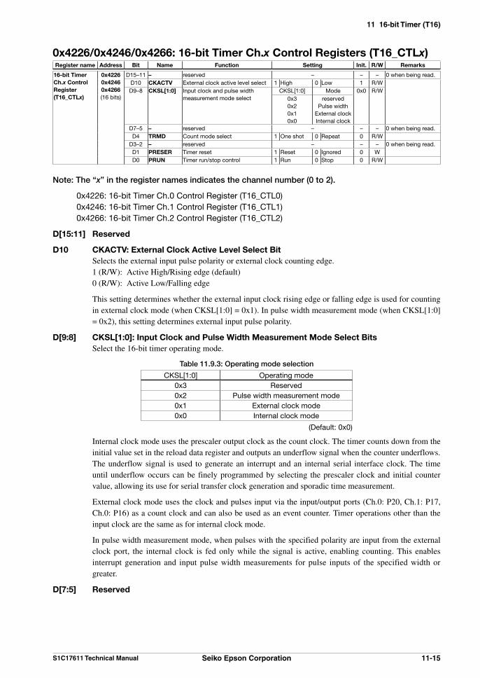
11 16-bit Timer (T16)
S1C17611 Technical Manual Seiko Epson Corporation 11-15
0x4226/0x4246/0x4266: 16-bit Timer Ch.x Control Registers (T16_CTLx)Register name Address Bit Name Function Setting Init. R/W Remarks
16-bit Timer Ch.x Control Register(T16_CTLx)
0x42260x42460x4266(16 bits)
D15–11 – reserved – – – 0 when being read.D10 CKACTV External clock active level select 1 High 0 Low 1 R/WD9–8 CKSL[1:0] Input clock and pulse width
measurement mode selectCKSL[1:0] Mode 0x0 R/W
0x30x20x10x0
reservedPulse width
External clockInternal clock
D7–5 – reserved – – – 0 when being read.D4 TRMD Count mode select 1 One shot 0 Repeat 0 R/W
D3–2 – reserved – – – 0 when being read.D1 PRESER Timer reset 1 Reset 0 Ignored 0 WD0 PRUN Timer run/stop control 1 Run 0 Stop 0 R/W
Note: The “x” in the register names indicates the channel number (0 to 2).
0x4226: 16-bit Timer Ch.0 Control Register (T16_CTL0) 0x4246: 16-bit Timer Ch.1 Control Register (T16_CTL1) 0x4266: 16-bit Timer Ch.2 Control Register (T16_CTL2)
D[15:11] Reserved
D10 CKACTV: External Clock Active Level Select Bit Selects the external input pulse polarity or external clock counting edge. 1 (R/W): Active High/Rising edge (default) 0 (R/W): Active Low/Falling edge
This setting determines whether the external input clock rising edge or falling edge is used for counting in external clock mode (when CKSL[1:0] = 0x1). In pulse width measurement mode (when CKSL[1:0] = 0x2), this setting determines external input pulse polarity.
D[9:8] CKSL[1:0]: Input Clock and Pulse Width Measurement Mode Select Bits Select the 16-bit timer operating mode.
Table 11.9.3: Operating mode selection
CKSL[1:0] Operating mode0x3 Reserved0x2 Pulse width measurement mode0x1 External clock mode0x0 Internal clock mode
(Default: 0x0)
Internal clock mode uses the prescaler output clock as the count clock. The timer counts down from the initial value set in the reload data register and outputs an underflow signal when the counter underflows. The underflow signal is used to generate an interrupt and an internal serial interface clock. The time until underflow occurs can be finely programmed by selecting the prescaler clock and initial counter value, allowing its use for serial transfer clock generation and sporadic time measurement.
External clock mode uses the clock and pulses input via the input/output ports (Ch.0: P20, Ch.1: P17, Ch.0: P16) as a count clock and can also be used as an event counter. Timer operations other than the input clock are the same as for internal clock mode.
In pulse width measurement mode, when pulses with the specified polarity are input from the external clock port, the internal clock is fed only while the signal is active, enabling counting. This enables interrupt generation and input pulse width measurements for pulse inputs of the specified width or greater.
D[7:5] Reserved

11 16-bit Timer (T16)
11-16 Seiko Epson Corporation S1C17611 Technical Manual
D4 TRMD: Count Mode Select Bit Selects the 16-bit timer count mode. 1 (R/W): One-shot mode 0 (R/W): Repeat mode (default)
Setting TRMD to 0 sets the 16-bit timer to Repeat mode. In this mode, once the count starts, the 16-bit timer continues to run until stopped by the application. If the counter underflows, the timer presets the counter to the reload data register value and continues the count. Thus, the timer periodically outputs an underflow pulse. Set the 16-bit timer to this mode to generate periodic interrupts at desired intervals or to generate a serial transfer clock.
Setting TRMD to 1 sets the 16-bit timer to One-shot mode. In this mode, the 16-bit timer stops automatically as soon as the counter underflows. This means only one interrupt can be generated after the timer starts. Note that the timer presets the counter to the reload data register value, then stops when an underflow occurs. Set the 16-bit timer to this mode to set a specific wait time or for pulse width measurement.
D[3:2] Reserved
D1 PRESER: Timer Reset Bit Resets the 16-bit timer. 1 (W): Reset 0 (W): Disabled 0 (R): Normally 0 when read out (default)
Writing 1 to this bit presets the counter to the reload data value.
D0 PRUN: Timer Run/Stop Control Bit Controls the timer RUN/STOP. 1 (R/W): Run 0 (R/W): Stop (default)
The timer starts counting when PRUN is written as 1 and stops when written as 0. When the timer is stopped, the counter data is retained until reset or until the next RUN state.

11 16-bit Timer (T16)
S1C17611 Technical Manual Seiko Epson Corporation 11-17
0x4228/0x4248/0x4268: 16-bit Timer Ch.x Interrupt Control Registers (T16_INTx)Register name Address Bit Name Function Setting Init. R/W Remarks
16-bit Timer Ch.x Interrupt Control Register(T16_INTx)
0x42280x42480x4268(16 bits)
D15–9 – reserved – – – 0 when being read.D8 T16IE 16-bit timer interrupt enable 1 Enable 0 Disable 0 R/W
D7–1 – reserved – – – 0 when being read.D0 T16IF 16-bit timer interrupt flag 1 Cause of
interrupt occurred
0 Cause of interrupt not occurred
0 R/W Reset by writing 1.
Note: The “x” in register names indicates the channel number (0 to 2).
0x4228: 16-bit Timer Ch.0 Interrupt Control Register (T16_INT0) 0x4248: 16-bit Timer Ch.1 Interrupt Control Register (T16_INT1) 0x4268: 16-bit Timer Ch.2 Interrupt Control Register (T16_INT2)
D[15:9] Reserved
D8 T16IE: 16-bit Timer Interrupt Enable Bit Permits or prevents interrupts caused by counter underflows for each channel. 1 (R/W): Permit interrupt 0 (R/W): Prevent interrupt (default)
Setting T16IE to 1 enables 16-bit timer interrupt requests to the ITC; setting to 0 prevents interrupts.
D[7:1] Reserved
D0 T16IF: 16-bit Timer Interrupt Flag Interrupt flag indicating the counter underflow interrupt cause occurrence status for each channel. 1 (R): Interrupt cause present 0 (R): No interrupt cause (default) 1 (W): Reset flag 0 (W): Disable
T16IF is the T16 module interrupt flag. Setting T16IE (D8) to 1 sets the counter to 1 if an underflow occurs during counting. A 16-bit timer interrupt request signal is output to the ITC at the same time. An interrupt is generated if interrupt conditions are satisfied for the ITC and S1C17 core.
Writing 1 to this bit resets T16IF.
Note: • To prevent interrupt recurrences, the T16 module interrupt flag T16IF must be reset within the interrupt processing routine following a 16-bit timer interrupt.
• To prevent unwanted interrupts, reset T16IF before permitting 16-bit timer interrupts with T16IE.
11 16-bit Timer (T16)
11-18 Seiko Epson Corporation S1C17611 Technical Manual
11.10 Precautions• The prescaler must run before the 16-bit timer.• Set the count clock and count mode only while the 16-bit timer count is stopped.• To prevent interrupt recurrences, the T16 module interrupt flag T16IF (D0/T16_INTx register) must be reset within
the interrupt processing routine following a 16-bit timer interrupt.
* T16IF: 16-bit Timer Interrupt Flag in the 16-bit Timer Ch.x Interrupt Control (T16_INTx) Register(D0/0x4228/0x4248/0x4268)
• To prevent unwanted interrupts, reset T16IF before permitting 16-bit timer interrupts with T16IE (D8/T16_INTx register).
* T16IE: 16-bit Timer Interrupt Enable Bit in the 16-bit Timer Ch.x Interrupt Control (T16_INTx) Register (D8/0x4228/0x4248/0x4268)

12 8-bit Timer (T8F)
S1C17611 TECHNICAL MANUAL Seiko Epson Corporation 12-1
12 8-bit Timer (T8F)
12.1 8-bit Timer OverviewThe S1C17611 incorporates an 1 channel 8-bit timer with Fine mode.The 8-bit timer consists of an 8-bit presettable down counter and an 8-bit reload data register holding the preset values. The timer counts down from the initial value set in the reload data register and outputs an underflow signal when the counter underflows. The underflow signal is used to generate an interrupt and UART clock. The underflow cycle can be programmed by selecting the prescaler clock and reload data, enabling the application program to obtain time intervals and serial transfer speeds as required. Fine mode provides a function that minimizes transfer rate errors.Figure 12.1.1 illustrates the 8-bit timer configuration.
Reload data registerT8F_TR
PRUN
DF[3:0]
PCLK•1/1 to 1/16 K
UnderflowRUN/STOP control
Inte
rnal
dat
a b
us
Fine mode setting
Interrupt request
Serial transfer clock
To ITCTo UART
(from T8F)
Timer reset
Down counterT8F_TC
Control circuit
PRESER
TFMD[3:0]
Prescaler
8-bit timer
Count clock selection
Figure 12.1.1: 8-bit timer configuration
12 8-bit Timer (T8F)
12-2 Seiko Epson Corporation S1C17611 TECHNICAL MANUAL
12.2 8-bit Timer Count ModeThe 8-bit timer features two count modes: Repeat mode and One-shot mode. These modes are selected using the TRMD bit (D4/T8F_CTL register).
* TRMD: Count Mode Select Bit in the 8-bit Timer Control (T8F_CTL) Register (D4/0x4206)
Repeat mode (TRMD = 0, default) Setting TRMD to 0 sets the 8-bit timer to Repeat mode. In this mode, once the count starts, the 8-bit timer continues running until stopped by the application program.
If the counter underflows, the timer presets the reload data register value into the counter and continues the count. Thus, the timer periodically outputs an underflow pulse. The 8-bit timer should be set to this mode to generate periodic interrupts at desired intervals or to generate a serial transfer clock.
One-shot mode (TRMD = 1) Setting TRMD to 1 sets the 8-bit timer to One-shot mode. In this mode, the 8-bit timer stops automatically as soon as the counter underflows. This means only one
interrupt can be generated after the timer starts. Note that the timer presets the reload data register value to the counter, then stops after an underflow has occurred. The 8-bit timer should be set to this mode to set a specific wait time.
Note: Make sure the 8-bit timer count is halted before changing count mode settings.
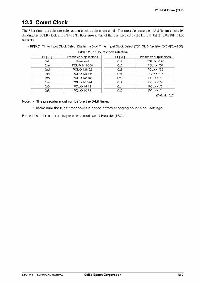
12 8-bit Timer (T8F)
S1C17611 TECHNICAL MANUAL Seiko Epson Corporation 12-3
12.3 Count ClockThe 8-bit timer uses the prescaler output clock as the count clock. The prescaler generates 15 different clocks by dividing the PCLK clock into 1/1 to 1/16 K divisions. One of these is selected by the DF[3:0] bit (D[3:0]/T8F_CLK register).
* DF[3:0]: Timer Input Clock Select Bits in the 8-bit Timer Input Clock Select (T8F_CLK) Register (D[3:0]/0x4200)
Table 12.3.1: Count clock selection
DF[3:0] Prescaler output clock DF[3:0] Prescaler output clock0xf Reserved 0x7 PCLK•1/1280xe PCLK•1/16384 0x6 PCLK•1/640xd PCLK•1/8192 0x5 PCLK•1/320xc PCLK•1/4096 0x4 PCLK•1/160xb PCLK•1/2048 0x3 PCLK•1/80xa PCLK•1/1024 0x2 PCLK•1/40x9 PCLK•1/512 0x1 PCLK•1/20x8 PCLK•1/256 0x0 PCLK•1/1
(Default: 0x0)
Note: • The prescaler must run before the 8-bit timer.
• Make sure the 8-bit timer count is halted before changing count clock settings.
For detailed information on the prescaler control, see “9 Prescaler (PSC).”

12 8-bit Timer (T8F)
12-4 Seiko Epson Corporation S1C17611 TECHNICAL MANUAL
12.4 8-bit Timer Reload Register and Underflow CycleThe reload data register T8F_TR (0x4202) is used to set the initial value for the down counter.The initial counter value set in the reload data register is preset to the down counter if the 8-bit timer is reset or the counter underflows. If the 8-bit timer is started after resetting, the timer counts down from the reload value (initial value). This means this reload value and the input clock frequency determines the time elapsed from the point at which the timer starts until the underflow occurs (or between underflows). The time determined is used to obtain the specified wait time, the intervals between periodic interrupts, and the programmable serial interface transfer clock.
One-shot mode
Counter
Repeat mode
Counter
01n-1n n
Preset by timer reset
Preset by timer reset
Auto preset
Underflow
Auto preset
(n = reload data)
01n-1n n
Underflow
Timer start
Timer start
Auto preset
01n-1 n
Underflow
Figure 12.4.1: Preset timing
The underflow cycle can be calculated as follows:
T8F_TR + 1 clk_inUnderflow interval = —————— [s] Underflow cycle = —————— [Hz] clk_in T8F_TR + 1
clk_in: Count clock (prescaler output clock) frequency [Hz] T8F_TR: Reload data (0 to 255)
Note: The UART generates a sampling clock that divides the 8-bit timer output into 1/16 divisions. Be careful when setting the transfer rate.

12 8-bit Timer (T8F)
S1C17611 TECHNICAL MANUAL Seiko Epson Corporation 12-5
12.5 8-bit Timer ResetThe 8-bit timer is reset by writing 1 to PRESER bit (D1/T8F_CTL register). The reload data is preset and the counter is initialized.
* PRESER: Timer Reset Bit in the 8-bit Timer Control (T8F_CTL) Register (D1/0x4206)
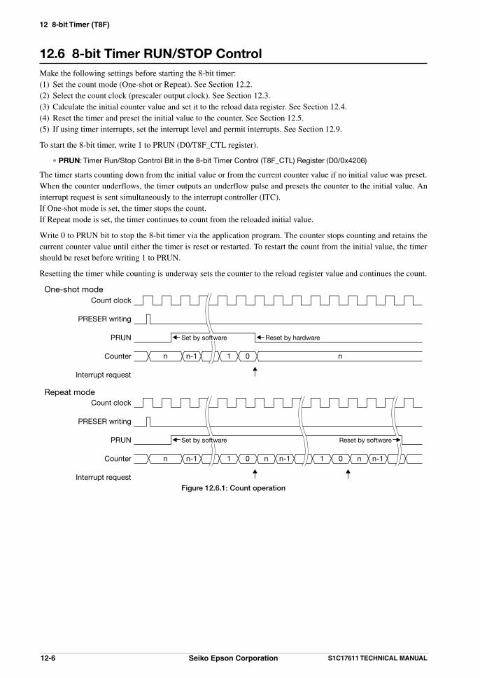
12 8-bit Timer (T8F)
12-6 Seiko Epson Corporation S1C17611 TECHNICAL MANUAL
12.6 8-bit Timer RUN/STOP ControlMake the following settings before starting the 8-bit timer:(1) Set the count mode (One-shot or Repeat). See Section 12.2.(2) Select the count clock (prescaler output clock). See Section 12.3.(3) Calculate the initial counter value and set it to the reload data register. See Section 12.4.(4) Reset the timer and preset the initial value to the counter. See Section 12.5.(5) If using timer interrupts, set the interrupt level and permit interrupts. See Section 12.9.
To start the 8-bit timer, write 1 to PRUN (D0/T8F_CTL register).
* PRUN: Timer Run/Stop Control Bit in the 8-bit Timer Control (T8F_CTL) Register (D0/0x4206)
The timer starts counting down from the initial value or from the current counter value if no initial value was preset. When the counter underflows, the timer outputs an underflow pulse and presets the counter to the initial value. An interrupt request is sent simultaneously to the interrupt controller (ITC).If One-shot mode is set, the timer stops the count.If Repeat mode is set, the timer continues to count from the reloaded initial value.
Write 0 to PRUN bit to stop the 8-bit timer via the application program. The counter stops counting and retains the current counter value until either the timer is reset or restarted. To restart the count from the initial value, the timer should be reset before writing 1 to PRUN.
Resetting the timer while counting is underway sets the counter to the reload register value and continues the count.
Count clock
PRESER writing
PRUN
Counter
Interrupt request
01n-1n n
Count clock
PRESER writing
PRUN
Counter
Interrupt request
01n-1n n 01n-1 n n-1
One-shot mode
Repeat mode
Reset by hardwareSet by software
Set by software Reset by software
Figure 12.6.1: Count operation

12 8-bit Timer (T8F)
S1C17611 TECHNICAL MANUAL Seiko Epson Corporation 12-7
12.7 8-bit Timer Output SignalThe 8-bit timer outputs underflow pulses when the counter underflows.These pulses are used for timer interrupt requests.
The underflow pulses are also used to generate the serial transfer clock and are transmitted to the UART.
8-bit timer output clock → UART
Use the following equations to calculate the reload data register value for obtaining the desired transfer rate.
clk_inbps = ————————————— (T8F_TR + 1) × 16 + TFMD clk_inT8F_TR = (——— - TFMD - 16) ÷ 16 bps
clk_in: Count clock (prescaler output clock) frequency [Hz]T8F_TR: Reload data (0 to 255)bps: Transfer rate (bit/s)TFMD: Fine mode setting (0 to15)

12 8-bit Timer (T8F)
12-8 Seiko Epson Corporation S1C17611 TECHNICAL MANUAL
12.8 Fine ModeFine mode provides a function that minimizes transfer rate errors.The 8-bit timer can output a programmable clock signal for use as the UART Ch.0 serial transfer clock. The timer output clock can be set to the required frequency by selecting the appropriate prescaler output clock and reload data. Note that errors may occur, depending on the transfer rate. Fine mode extends the output clock cycle by delaying the underflow pulse from the counter. This delay can be specified with the TFMD[3:0] bit (D[11:8]/T8F_CTL register).
* TFMD[3:0]: Fine Mode Setup Bits in the 8-bit Timer Control (T8F_CTL) Register (D[11:8]/0x4206)
The TFMD[3:0] bit specifies the delay pattern to be inserted into the 16 underflow intervals. Inserting one delay extends the output clock cycle by one count clock cycle. This setting delays the interrupt timing in the same way.
Table 12.8.1: Delay patterns specified by TFMD[3:0]
TFMD[3:0]Underflow number
1 2 3 4 5 6 7 8 9 10 11 12 13 14 15 160x0 – – – – – – – – – – – – – – – –0x1 – – – – – – – – – – – – – – – D0x2 – – – – – – – D – – – – – – – D0x3 – – – – – – – D – – – D – – – D0x4 – – – D – – – D – – – D – – – D0x5 – – – D – – – D – – – D – D – D0x6 – – – D – D – D – – – D – D – D0x7 – – – D – D – D – D – D – D – D0x8 – D – D – D – D – D – D – D – D0x9 – D – D – D – D – D – D – D D D0xa – D – D – D D D – D – D – D D D0xb – D – D – D D D – D D D – D D D0xc – D D D – D D D – D D D – D D D0xd – D D D – D D D – D D D D D D D0xe – D D D D D D D – D D D D D D D0xf – D D D D D D D D D D D D D D D
D: Indicates the insertion of a delay cycle.
Count clock
Underflow signal (no correction)
Underflow signal (with correction)
Output clock (no correction)
Output clock (with correction)
Delay
15 16
15 16
1
1
Figure 12.8.1: Delay cycle insertion in Fine mode
After the initial resetting, TFMD[3:0] is set to 0x0, preventing insertion of delay cycles.
12 8-bit Timer (T8F)
S1C17611 TECHNICAL MANUAL Seiko Epson Corporation 12-9
12.9 8-bit Timer InterruptsThe 8-bit timer outputs interrupt requests to the interrupt controller (ITC) when the counter underflows.
Underflow interrupt This interrupt request generated by a counter underflow sets the interrupt flag T8IF (D0/T8F_INT register) to 1
within the T8F module.* T8IF: 8-bit Timer Interrupt Flag in the 8-bit Timer Interrupt Control (T8F_INT) Register (D0/0x4208)
To use this interrupt, set T8IE (D8/T8F_INT register) to 1. If T8IE is set to 0 (the default value), T8IF will not be set to 1, and interrupt request for this interrupt cause will not be sent to the ITC.
* T8IE: 8-bit Timer Interrupt Enable Bit in the 8-bit Timer Interrupt Control (T8F_INT) Register (D8/0x4208)
If T8IF is set to 1, the T8F module outputs an interrupt request to the ITC. An interrupt is generated if interrupt conditions are satisfied for the ITC and S1C17 core.
Note: • To prevent interrupt recurrences, the T8F module interrupt flag T8IF must be reset within the interrupt processing routine following an 8-bit timer interrupt.
• To prevent unwanted interrupts, reset T8IF before permitting 8-bit timer interrupts with T8IE.
Interrupt vectors The 8-bit timer interrupt vector numbers and vector addresses are listed below.
Vector number: 12 (0x0c) Vector address: TTBR + 0x30
Other interrupt settings The ITC allows the priority of 8-bit timer interrupts to be set between level 0 (the default value) and level 7. To
generate actual interrupts, the PSR (S1C17 core internal processor status register) IE (interrupt enable) bit must be set to 1.
For more information on interrupt processing, see “6 Interrupt Controller (ITC).”

12 8-bit Timer (T8F)
12-10 Seiko Epson Corporation S1C17611 TECHNICAL MANUAL
12.10 Control Register DetailsTable 12.10.1: 8-bit timer register list
Address Register name Function0x4200 T8F_CLK 8-bit Timer Input Clock Select Register Prescaler output clock selection0x4202 T8F_TR 8-bit Timer Reload Data Register Reload data setting0x4204 T8F_TC 8-bit Timer Counter Data Register Counter data0x4206 T8F_CTL 8-bit Timer Control Register Timer mode setting and timer RUN/STOP0x4208 T8F_INT 8-bit Timer Interrupt Control Register Interrupt control
The 8-bit timer registers are described in detail below. These are 16-bit registers.
Note: When data is written to the registers, the “Reserved” bits must always be written as 0 and not 1.

12 8-bit Timer (T8F)
S1C17611 TECHNICAL MANUAL Seiko Epson Corporation 12-11
0x4200: 8-bit Timer Input Clock Select Register (T8F_CLK)Register name Address Bit Name Function Setting Init. R/W Remarks
8-bit Timer Input Clock Select Register(T8F_CLK)
0x4200(16 bits)
D15–4 – reserved – – – 0 when being read.D3–0 DF[3:0] 8-bit timer input clock select
(Prescaler output clock)DF[3:0] Clock 0x0 R/W
0xf0xe0xd0xc0xb0xa0x90x80x70x60x50x40x30x20x10x0
reservedPCLK•1/16384PCLK•1/8192PCLK•1/4096PCLK•1/2048PCLK•1/1024PCLK•1/512PCLK•1/256PCLK•1/128PCLK•1/64PCLK•1/32PCLK•1/16PCLK•1/8PCLK•1/4PCLK•1/2PCLK•1/1
D[15:4] Reserved
D[3:0] DF[3:0]: Timer Input Clock Select Bits Select the 8-bit timer count clock from the 15 different prescaler output clocks.
Table 12.10.2: Count clock selection
DF[3:0] Prescaler output clock DF[3:0] Prescaler output clock0xf Reserved 0x7 PCLK•1/1280xe PCLK•1/16384 0x6 PCLK•1/640xd PCLK•1/8192 0x5 PCLK•1/320xc PCLK•1/4096 0x4 PCLK•1/160xb PCLK•1/2048 0x3 PCLK•1/80xa PCLK•1/1024 0x2 PCLK•1/40x9 PCLK•1/512 0x1 PCLK•1/20x8 PCLK•1/256 0x0 PCLK•1/1
(Default: 0x0)
Note: Make sure the 8-bit timer count is halted before changing count clock settings.

12 8-bit Timer (T8F)
12-12 Seiko Epson Corporation S1C17611 TECHNICAL MANUAL
0x4202: 8-bit Timer Reload Data Register (T8F_TR)Register name Address Bit Name Function Setting Init. R/W Remarks
8-bit Timer Reload Data Register(T8F_TR)
0x4202(16 bits)
D15–8 – reserved – – – 0 when being read.D7–0 TR[7:0] 8-bit timer reload data
TR7 = MSBTR0 = LSB
0x0 to 0xff 0x0 R/W
D[15:8] Reserved
D[7:0] TR[7:0]: 8-bit Timer Reload Data Sets the counter initial value. (Default: 0x0) The reload data set in this register is preset to the counter if the timer is reset or the counter underflows. If the 8-bit timer is started after resetting, the timer counts down from the reload value (initial value).
This means this reload value and the input clock frequency determine the time elapsed from the point at which the timer starts until the underflow occurs (or between underflows). The time determined is used to obtain the desired wait time, the intervals between periodic interrupts, and the programmable serial interface transfer clock.

12 8-bit Timer (T8F)
S1C17611 TECHNICAL MANUAL Seiko Epson Corporation 12-13
0x4204: 8-bit Timer Counter Data Register (T8F_TC)Register name Address Bit Name Function Setting Init. R/W Remarks
8-bit Timer Counter Data Register(T8F_TC)
0x4204(16 bits)
D15–8 – reserved – – – 0 when being read.D7–0 TC[7:0] 8-bit timer counter data
TC7 = MSBTC0 = LSB
0x0 to 0xff 0xff R
D[15:8] Reserved
D[7:0] TC[7:0]: 8-bit Timer Counter Data Reads out the counter data. (Default: 0xff) This register is read-only and cannot be written to.

12 8-bit Timer (T8F)
12-14 Seiko Epson Corporation S1C17611 TECHNICAL MANUAL
0x4206: 8-bit Timer Control Register (T8F_CTL)Register name Address Bit Name Function Setting Init. R/W Remarks
8-bit Timer Control Register(T8F_CTL)
0x4206(16 bits)
D15–12 – reserved – – – 0 when being read.D11–8 TFMD[3:0] Fine mode setup 0x0 to 0xf 0x0 R/W Set a number of times
to insert delay into a 16-underflow period.
D7–5 – reserved – – – 0 when being read.D4 TRMD Count mode select 1 One shot 0 Repeat 0 R/W
D3–2 – reserved – – – 0 when being read.D1 PRESER Timer reset 1 Reset 0 Ignored 0 WD0 PRUN Timer run/stop control 1 Run 0 Stop 0 R/W
D[15:12] Reserved
D[11:8] TFMD[3:0]: Fine Mode Setup Bits Correct the transfer rate error. (Default: 0x0) The TFMD[3:0] bit specifies the delay pattern to be inserted into the 16 underflow intervals. Inserting
one delay extends the output clock cycle by one count clock cycle. This setting delays the interrupt timing in the same way.
Table 12.10.3: Delay patterns specified by TFMD[3:0]
TFMD[3:0]Underflow number
1 2 3 4 5 6 7 8 9 10 11 12 13 14 15 160x0 – – – – – – – – – – – – – – – –0x1 – – – – – – – – – – – – – – – D0x2 – – – – – – – D – – – – – – – D0x3 – – – – – – – D – – – D – – – D0x4 – – – D – – – D – – – D – – – D0x5 – – – D – – – D – – – D – D – D0x6 – – – D – D – D – – – D – D – D0x7 – – – D – D – D – D – D – D – D0x8 – D – D – D – D – D – D – D – D0x9 – D – D – D – D – D – D – D D D0xa – D – D – D D D – D – D – D D D0xb – D – D – D D D – D D D – D D D0xc – D D D – D D D – D D D – D D D0xd – D D D – D D D – D D D D D D D0xe – D D D D D D D – D D D D D D D0xf – D D D D D D D D D D D D D D D
D: Indicates the insertion of a delay cycle.
Count clock
Underflow signal (no correction)
Underflow signal (with correction)
Output clock (no correction)
Output clock (with correction)
Delay
15 16
15 16
1
1
Figure 12.10.1: Delay cycle insertion in Fine mode
D[7:5] Reserved

12 8-bit Timer (T8F)
S1C17611 TECHNICAL MANUAL Seiko Epson Corporation 12-15
D4 TRMD: Count Mode Select Bit Selects the 8-bit timer count mode. 1 (R/W): One-shot mode 0 (R/W): Repeat mode (default)
Setting TRMD to 0 sets the 8-bit timer to Repeat mode. In this mode, once the count starts, the 8-bit timer continues to run until stopped by the application. If the counter underflows, the timer presets the counter to the reload data register value and continues the count. Thus, the timer periodically outputs an underflow pulse. Set the 8-bit timer to this mode to generate periodic interrupts at desired intervals or to generate a serial transfer clock.
Setting TRMD to 1 sets the 8-bit timer to One-shot mode. In this mode, the 8-bit timer stops automatically as soon as the counter underflows. This means only one interrupt can be generated after the timer starts. Note that the timer presets the counter to the reload data register value, then stops when an underflow occurs. Set the 8-bit timer to this mode to set a specific wait time.
Note: Make sure the 8-bit timer count is halted before changing count mode settings.
D[3:2] Reserved
D1 PRESER: Timer Reset Bit Resets the 8-bit timer. 1 (W): Reset 0 (W): Disabled 0 (R): Normally 0 when read out (default)
Writing 1 to this bit presets the counter to the reload data value.
D0 PRUN: Timer Run/Stop Control Bit Controls the timer RUN/STOP. 1 (R/W): Run 0 (R/W): Stop (default)
The timer starts counting when PRUN is written as 1 and stops when written as 0. When the timer is stopped, the counter data is retained until reset or until the next RUN state.

12 8-bit Timer (T8F)
12-16 Seiko Epson Corporation S1C17611 TECHNICAL MANUAL
0x4208: 8-bit Timer Interrupt Control Register (T8F_INT)Register name Address Bit Name Function Setting Init. R/W Remarks
8-bit TimerInterrupt Control Register(T8F_INT)
0x4208(16 bits)
D15–9 – reserved – – – 0 when being read.D8 T8IE 8-bit timer interrupt enable 1 Enable 0 Disable 0 R/W
D7–1 – reserved – – – 0 when being read.D0 T8IF 8-bit timer interrupt flag 1 Cause of
interrupt occurred
0 Cause of interrupt not occurred
0 R/W Reset by writing 1.
D[15:9] Reserved
D8 T8IE: 8-bit Timer Interrupt Enable Bit Permits or prevents interrupts caused by counter underflows for each channel. 1 (R/W): Permit interrupt 0 (R/W): Prevent interrupt (default)
Setting T8IE to 1 permits 8-bit timer interrupt requests to the ITC; setting to 0 prevents interrupts.
D[7:1] Reserved
D0 T8IF: 8-bit Timer Interrupt Flag Interrupt flag indicating the counter underflow interrupt cause occurrence status for each channel. 1 (R): Interrupt cause present 0 (R): No interrupt cause (default) 1 (W): Reset flag 0 (W): Disable
T8IF is the T8F module interrupt flag. Setting T8IE (D8) to 1 sets the counter to 1 if an underflow occurs during counting. An 8-bit timer interrupt request signal is output to the ITC at the same time. An interrupt is generated if interrupt conditions are satisfied for the ITC and S1C17 core.
Writing 1 to this bit resets T8IF.
Note: • To prevent interrupt recurrences, the T8F module interrupt flag T8IF must be reset within the interrupt processing routine following an 8-bit timer interrupt.
• To prevent unwanted interrupts, reset T8IF before permitting 8-bit timer interrupts with T8IE.

12 8-bit Timer (T8F)
S1C17611 TECHNICAL MANUAL Seiko Epson Corporation 12-17
12.11 Precautions• The prescaler must run before the 8-bit timer.• Set the count clock and count mode only while the 8-bit timer count is stopped.• To prevent interrupt recurrences, the T8F module interrupt flag T8IF (D0/T8F_INT register) must be reset within
the interrupt processing routine following an 8-bit timer interrupt.
* T8IF: 8-bit Timer Interrupt Flag in the 8-bit Timer Interrupt Control (T8F_INT) Register (D0/0x4208)
• To prevent unwanted interrupts, reset T8IF before permitting 8-bit timer interrupts with T8IE (D8/T8F_INT register).
* T8IE: 8-bit Timer Interrupt Enable Bit in the 8-bit Timer Interrupt Control (T8F_INT) Register (D8/0x4208)

13 PWM Timer (T16E)
S1C17611 TECHNICAL MANUAL Seiko Epson Corporation 13-1
13 PWM Timer (T16E)
13.1 PWM Timer OverviewThe S1C17611 incorporates the 2-channel PWM Timer.Figure 13.1.1 illustrates the PWM Timer configuration.
T16EDF[3:0]
Inte
rnal
dat
a b
us
PWM outputP12, P15/TOUT3P05, P11/TOUT4
P13/TOUTN3P10/TOUTN4
P05/EXCL3P14/EXCL4
Countcontrolcircuit
Output controlcircuit
Interrupt controlcircuit
CLKSEL
T16ERUN
OUTEN
INITOL
INVOUT
SELFM
T16ERST
CBUFEN
CAIE
CBIE
PWM timer Ch.x
Compare data A registerT16E_CA
PCLK•1/1 to 1/16K
Prescaler clock selection
Compare A interrupt requestCompare B interrupt requestTo ITC
Compare data B registerT16E_CB
Compare A signal
Up-counterT16E_TC
Comparator
Input clock selection
RUN/STOP control
Clock output enable
Initial output level selection
Inverted output
Fine mode selection
Timer reset
Compare buffer enable
Compare A interrupt enable
Compare B interrupt enable
Prescaler
Compare data A buffer(T16E_CA)
Compare data B buffer(T16E_CB)
Compare B signal
Comparator
Figure 13.1.1: PWM Timer configuration
The PWM Timer includes a 16-bit up-counter (T16E_TC register), two 16-bit compare data registers (T16E_CA and T16E_CB registers), and the corresponding buffers.
Software can configure the count value of the 16-bit counter, and reset it to 0, while an external signal from the input/output port pin (EXCLx) or the Prescaler output clock counts up the 16-bit counter. Software can read the count value.
The compare data A and B registers hold data for comparison against the up-counter contents. Data can be read or written directly to or from the compare data registers. The compare data buffers enables loading to the compare data registers of comparison values set when the counter is reset by software or by a compare B match signal. Software can be used to set which of the compare data register and buffer the comparison values are written to.
If the counter value matches the contents of each compare data register, the comparator outputs a signal to control interrupts and output signals. These registers can be used to program the interrupt occurrence cycle and output clock frequency and duty ratio.
Note: The 2-channel PWM timer has the same functions for both channels. Only the control register addresses are different. The description in this section applies to all PWM timer channels. The “x” in the register name indicates the channel number (0 or 1). Register addresses are given in the format (Ch.0/Ch.1).Example: T16E_CTLx register (0x5306/0x5366)
Ch.0: T16E_CTL0 register (0x5306) Ch.1: T16E_CTL1 register (0x5366)

13 PWM Timer (T16E)
13-2 Seiko Epson Corporation S1C17611 TECHNICAL MANUAL
13.2 PWM Timer Operating ModesThe PWM Timer has the following two operating modes:1. Internal clock mode (Timer counting internal clock)2. External clock mode (Functions as event counter)
The operating mode is selected using CLKSEL (D3/T16E_CTLx register).
* CLKSEL: Input Clock Select Bit in the PWM Timer Ch.x Control (T16E_CTLx) Register (D3/0x5306/0x5366)
Setting CLKSEL to 0 (default) selects internal clock mode, while setting to 1 selects external clock mode.
Internal clock mode Internal clock mode uses the prescaler output clock as the count clock. The count clock is selected by the T16EDF[3:0] (D[3:0]/T16E_CLKx register) from the 15 types generated by
the prescaler dividing the PCLK clock into 1/1 to 1/16 K divisions.
* T16EDF[3:0]: Timer Input Clock Select Bits in the PWM Timer Ch.x Input Clock Select (T16E_CLKx) Register (D[3:0]/0x5308/0x5368)
Table 13.2.1: Prescaler clock selection
T16EDF[3:0] Prescaler output clock T16EDF[3:0] Prescaler output clock0xf Reserved 0x7 PCLK•1/1280xe PCLK•1/16384 0x6 PCLK•1/640xd PCLK•1/8192 0x5 PCLK•1/320xc PCLK•1/4096 0x4 PCLK•1/160xb PCLK•1/2048 0x3 PCLK•1/80xa PCLK•1/1024 0x2 PCLK•1/40x9 PCLK•1/512 0x1 PCLK•1/20x8 PCLK•1/256 0x0 PCLK•1/1
(Default: 0x0)
Note: • The prescaler must run before operating the PWM Timer in internal clock mode.
• Make sure the PWM Timer count is halted before changing count clock settings.
For detailed information on the prescaler control, see “9 Prescaler (PSC).”
External clock mode In external clock mode, channel 0 uses a clock or pulse input via the P05 (EXCL3) port and channel 1 uses
a clock or pulse input via the P14 (EXCL4) as the count clock. Therefore it can be used as an event counter. Timer operations other than input clock are the same as those in the internal clock mode.
To input the EXCL3 or EXCL4 clock via the P05 or P14 port, write 0 to the P05MUX (D3-2/P0_PMUX register) or P14MUX (D1-0/P1_PMUX register) to change the pin function, and set it to the input mode.
* P05MUX: P05 Port Function Select Bit in the P0 Port Function Select (P0_PMUX) Register (D3-2/0x52a1)* P14MUX: P14 Port Function Select Bit in the P1 Port Function Select (P1_PMUX) Register (D1-0/0x52a3)
The PWM Timer increments counts based on the input signal rising edge.
The PWM Timer does not use the prescaler in this mode. If no other peripheral modules are using the prescaler clock, the prescaler can be stopped to reduce current consumption.
For the input rules of external clock, see “28.11 External Clock Input Characteristics”.

13 PWM Timer (T16E)
S1C17611 TECHNICAL MANUAL Seiko Epson Corporation 13-3
13.3 Setting and Resetting Counter ValueReset the PWM timer counter by writing 1 to the T16ERST bit (D1/T16E_CTLx register). This clears the counter to 0.
* T16ERST: Timer Reset Bit in the PWM Timer Ch.x Control (T16E_CTLx) Register (D1/0x5306/0x5366)
Normally, the counter should be reset by writing 1 to this bit before starting the count up.The counter is reset by hardware if the counter matches compare data B after the count starts.
The counter can also be set to any desired value by writing data to T16ETC[15:0] (D[15:0]/T16E_TCx register).
* T16ETC[15:0]: Counter Data in the PWM Timer Ch.x Counter Data (T16E_TCx) Register (D[15:0]/0x5304/0x5364)

13 PWM Timer (T16E)
13-4 Seiko Epson Corporation S1C17611 TECHNICAL MANUAL
13.4 Compare Data Settings
Compare data register/buffer selection The PWM Timer incorporates a data comparator allowing comparison of counter data against any desired value.
This comparison data is stored in the compare data A and B registers. Data can be read or written directly to or from the compare data registers.
The compare data buffers enable automatic loading to the compare data registers of the comparison values set in the buffers when the counter is reset by software (writing 1 to T16ERST) or by a compare B match signal. The CBUFEN (D5/T16E_CTLx resister) is used to set which of the compare data register and buffer the comparison values are written to.
* CBUFEN: Comparison Buffer Enable Bit in the PWM Timer Ch.x Control (T16E_CTLx) Register (D5/0x5306/ 0x5366)
Writing 1 to CBUFEN selects the compare data buffer. Writing 0 to it selects the compare data register. The compare data register is selected after initial resetting.
Compare data writing Compare data A is written to T16ECA[15:0] (D[15:0]/T16E_CAx register). Compare data B is written to
T16ECB[15:0] (D[15:0]/T16E_CBx register).
* T16ECA[15:0]: Compare Data A in the PWM Timer Ch.x Compare Data A (T16E_CAx) Register (D[15:0]/0x5300/0x5360)
* T16ECB[15:0]: Compare Data B in the PWM Timer Ch.x Compare Data B (T16E_CBx) Register (D[15:0]/0x5302/0x5362)
When CBUFEN is set to 0, the compare data register values can be read or written directly by these registers. When CBUFEN is set to 1, data is read from and written to these registers via the compare data buffers. The
buffer contents are loaded into the compare data registers when the counter is reset. The compare data registers and buffers are set to 0x0 after initial resetting.
The timer compares the count data against the compare data registers and generates a compare match signal if the values are equal. This compare match signal generates an interrupt and controls the clock (TOUTx/TOUTNx signal) output externally.
Compare data B also determines the counter reset cycle. The counter reset cycle can be calculated as follows:
CB + 1 Counter reset interval= ———— [s] clk_in
clk_in Counter reset cycle = ———— [Hz] CB + 1
CB: Compare data B (T16E_CBx register value) clk_in: Prescaler output clock frequency

13 PWM Timer (T16E)
S1C17611 TECHNICAL MANUAL Seiko Epson Corporation 13-5
13.5 PWM Timer RUN/STOP ControlSet the following before starting the PWM Timer.(1) Set the operating mode (input clock). See Section 13.2.(2) Set the clock output. See Section 13.6.(3) If using interrupts, set the interrupt level and permit interrupts for the PWM Timer. See Section 13.7.(4) Set the counter value or reset to 0. See Section 13.3.(5) Set the compare data. See Section 13.4.
The PWM Timer includes T16ERUN (D0/T16E_CTLx register) to control Run/Stop.
* T16ERUN: Timer Run/Stop Control Bit in the PWM Timer Ch.x Control (T16E_CTLx) Register (D0/0x5306/0x5366)
The timer starts counting when T16ERUN is written as 1. Writing 0 to T16ERUN prevents clock input and stops the count.This control does not affect the counter data. The counter data is retained even when the count is halted, allowing resumption of the count from that data.If T16ERUN and T16ERST are written as 1 simultaneously, the timer starts counting after the reset.
If the counter matches the compare data A register setting during counting, a compare A match signal is output and a compare A interrupt factor generated.Likewise, if the counter matches the compare data B register setting, a compare B match signal is output and a compare B interrupt factor generated. The counter is reset to 0 at the same time. If CBUFEN is set to 1, the value set in the compare data buffers is loaded into the compare data registers. If interrupts are permitted, an interrupt request is sent to the interrupt controller (ITC).In either case, counting continues unaffected. For compare B, counting starts from the counter value 0.
T16ERUN
T16ERST
T16E_CA
T16E_CB
Input clock
T16E_TC
Reset Compare Ainterrupt
Reset andcompare B
interrupt
Compare Ainterrupt
Reset andcompare B
interrupt
0x2
0 1 2 3 4 5 0 1 2 3 4 5 0 1
0x5
Figure 13.5.1: Basic counter operation timing

13 PWM Timer (T16E)
13-6 Seiko Epson Corporation S1C17611 TECHNICAL MANUAL
13.6 Clock Output ControlThe PWM Timer can generate a TOUTx/TOUTNx signal using the compare match signal.Figure 13.6.1 shows the PWM Timer clock output circuit.
Logic
Clock OUTEN
TOUT3 (P12, P15)TOUT4 (P05, P11)
TOUTN3 (P13)TOUTN4 (P10)
INVOUT
D Q
Q
INITOLCompare ACompare B
Figure 13.6.1: PWM Timer clock output circuit
Initial output level settings The default output level is 0 (Low level) while the TOUTx clock output is Off (TOUTNx output is High
level). This can be changed to 1 (TOUTx = High level, TOUTNx = Low level) with INITOL (D8/T16E_CTLx register).
* INITOL: Initial Output Level Select Bit in the PWM Timer Ch.x Control (T16E_CTLx) Register (D8/0x5306/0x5366)
When INITOL is 0 (default), TOUTx initial output level is low (TOUTNx output is High). When INITOL is set to 1, the initial output level should be high (TOUTNx output is Low).
Output signal polarity selection By default, an active High (normal Low) TOUTx output signal is generated (TOUTNx output signal is active
Low). This logic can be inverted by INVOUT (D4/T16E_CTLx register). Writing 1 to INVOUT causes the timer to generate an active Low (normal High) TOUTx signal (TOUTNx signal is active High).
* INVOUT: Inverse Output Control Bit in the PWM Timer Ch.x Control (T16E_CTLx) Register (D4/0x5306/0x5366)
Setting INVOUT to 1 also inverts the initial output level set for INITOL. See Figure 13.6.2 for more information on output waveforms.
Output pin settings The TOUTx/TOUTNx signal generated here can be output from the following pins and can provide a
programmable clock and PWM signal to external devices. Ch.0: TOUT3 output → TOUT3 (P12, P15) pin, TOUTN3 output → TOUTN3 (P13) pin Ch.1: TOUT4 output → TOUT4 (P05, P11) pin, TOUTN4 output → TOUTN4 (P10) pin
The pin used for output is set for input/output port use after initial resetting and switches to input mode. The pin then becomes high-impedance.
Switching the pin function to TOUTx/TOUTNx output outputs the level set by INITOL and INVOUT. After the timer output starts, the output is maintained at this level until changed by the counter value.
Table 13.6.1: Initial output level
INITOL INVOUT Initial output level1 1 Low1 0 High0 1 High0 0 Low

13 PWM Timer (T16E)
S1C17611 TECHNICAL MANUAL Seiko Epson Corporation 13-7
Clock output start To output the TOUTx clock, write 1 to OUTEN (D2/T16E_CTLx register). Writing 0 to OUTEN switches the
output to the initial output level as set by INITOL and INVOUT.
* OUTEN: Clock Output Enable Bit in the PWM Timer Ch.x Control (T16E_CTLx) Register (D2/0x5306/0x5366)
Figure 13.6.2 illustrates the output waveform.
Input clock
T16ERST
OUTEN
T16ERUN
Counter value
Compare A signal
Compare B signal
TOUTx output (INITOL = 0, INVOUT = 0)
TOUTx output (INITOL = 0, INVOUT = 1)
TOUTx output (INITOL = 1, INVOUT = 0)
TOUTx output (INITOL = 1, INVOUT = 1)
(When T16E_CA = 3 and T16E_CB = 5)
1 2 3 4 5 00 1 2 3 4 5 0 1 2 3 4 5 0 1
Figure 13.6.2: PWM Timer output waveform
TOUTx output when INVOUT = 0 (Active High) The timer outputs Low level (initial output level at output start) until the counter matches the compare data A
set in the T16E_CAx register (0x5300/0x5360). When the counter reaches the next compare data A value, the output pin switches to High level, and a compare A interrupt factor is generated. If the counter subsequently counts up to compare data B set in the T16E_CBx register (0x5302/0x5362), the counter is reset and the output pin is returned to the Low level. A compare B interrupt factor is also generated at the same time.
The TOUTNx pins output the inverted signals described above.
TOUTx output when INVOUT = 1 (Active Low) The timer outputs High level (inverted value of the initial output level at output start) until the counter matches
the compare data A set in the T16E_CAx register (0x5300/0x5360). When the counter reaches the next compare data A value, the output pin switches to Low level, and a compare A interrupt factor is generated. If the counter subsequently counts up to compare data B set in the T16E_CBx register (0x5302/0x5362), the counter is reset and the output pin is returned to the High level. A compare B interrupt factor is also generated at the same time.
The TOUTNx pins output the inverted signals described above.
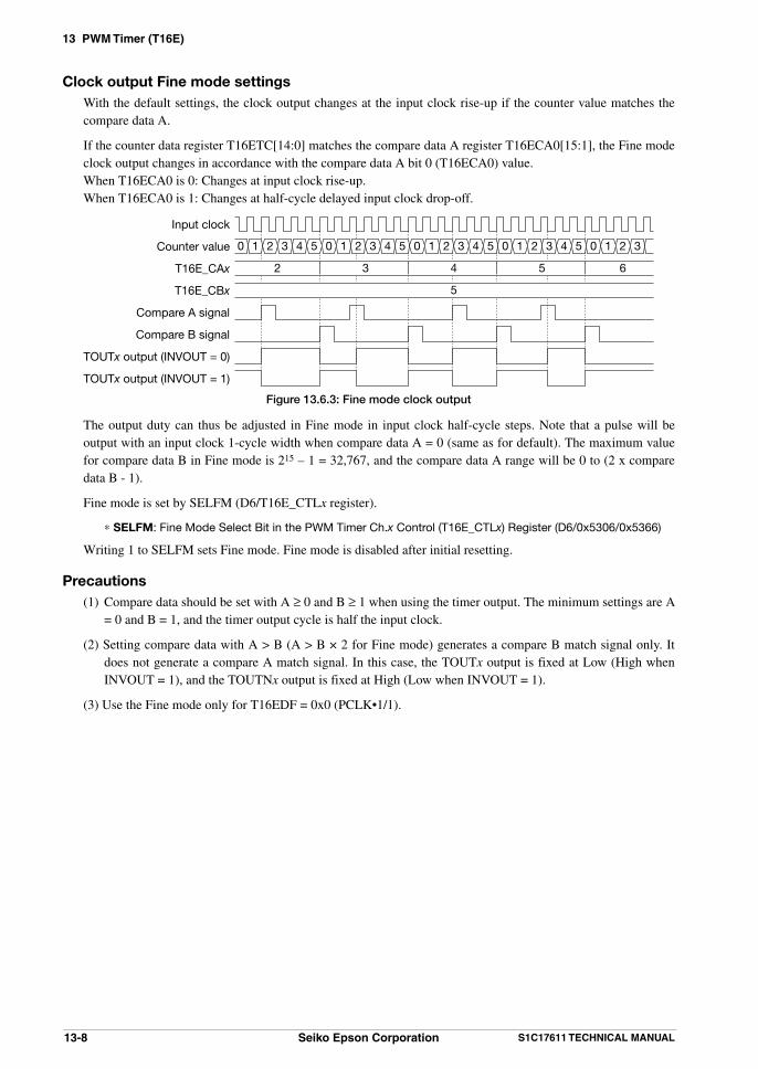
13 PWM Timer (T16E)
13-8 Seiko Epson Corporation S1C17611 TECHNICAL MANUAL
Clock output Fine mode settings With the default settings, the clock output changes at the input clock rise-up if the counter value matches the
compare data A.
If the counter data register T16ETC[14:0] matches the compare data A register T16ECA0[15:1], the Fine mode clock output changes in accordance with the compare data A bit 0 (T16ECA0) value.
When T16ECA0 is 0: Changes at input clock rise-up. When T16ECA0 is 1: Changes at half-cycle delayed input clock drop-off.
Input clock
Counter value
T16E_CAx
T16E_CBx
Compare A signal
Compare B signal
TOUTx output (INVOUT = 0)
TOUTx output (INVOUT = 1)
0
2 3 4 5 6
1 2 3 4 5 0 1 2 3 4 5 0 1 2 3 4 5 0 1 2 3 4 5 0 1 2 3
5
Figure 13.6.3: Fine mode clock output
The output duty can thus be adjusted in Fine mode in input clock half-cycle steps. Note that a pulse will be output with an input clock 1-cycle width when compare data A = 0 (same as for default). The maximum value for compare data B in Fine mode is 215 – 1 = 32,767, and the compare data A range will be 0 to (2 x compare data B - 1).
Fine mode is set by SELFM (D6/T16E_CTLx register).
* SELFM: Fine Mode Select Bit in the PWM Timer Ch.x Control (T16E_CTLx) Register (D6/0x5306/0x5366)
Writing 1 to SELFM sets Fine mode. Fine mode is disabled after initial resetting.
Precautions(1) Compare data should be set with A ≥ 0 and B ≥ 1 when using the timer output. The minimum settings are A
= 0 and B = 1, and the timer output cycle is half the input clock.
(2) Setting compare data with A > B (A > B × 2 for Fine mode) generates a compare B match signal only. It does not generate a compare A match signal. In this case, the TOUTx output is fixed at Low (High when INVOUT = 1), and the TOUTNx output is fixed at High (Low when INVOUT = 1).
(3) Use the Fine mode only for T16EDF = 0x0 (PCLK•1/1).
13 PWM Timer (T16E)
S1C17611 TECHNICAL MANUAL Seiko Epson Corporation 13-9
13.7 PWM Timer InterruptsThe T16E module includes functions for generating the following two kinds of interrupts:• Compare A match interrupt• Compare B match interrupt
The T16E module outputs a single interrupt signal shared by the above two interrupt factors to the interrupt controller (ITC). (Two channels output two interrupt signals in total.) The interrupt flag within the T16E module should be read to identify the interrupt factor that occurred.
Compare A match interrupt This interrupt request is generated when the counter matches the compare data A register setting during
counting. It sets the interrupt flag CAIF (D0/T16E_INTx register) within the T16E module to 1.
* CAIF: Compare A Interrupt Flag in the PWM Timer Ch.x Interrupt Flag (T16E_IFLGx) Register (D0/0x530c/0x536c)
To use this interrupt, set CAIE (D0/T16E_IMSKx register) to 1. If CAIE is set to 0 (default), CAIF is not set to 1, and the interrupt request for this factor is not sent to the ITC.
* CAIE: Compare A Interrupt Enable Bit in the PWM Timer Ch.x Interrupt Mask (T16E_IMSKx) Register (D0/0x530a/0x536a)
If CAIF is set to 1, the T16E module outputs an interrupt request to the ITC. An interrupt is generated if the ITC and S1C17 core interrupt conditions are satisfied.
CAIF should be read and checked within the PWM Timer interrupt processing routine to determine whether the PWM Timer interrupt is attributable to compare A matching.
Compare B match interrupt This interrupt request is generated when the counter matches the compare data B register setting during
counting. It sets the interrupt flag CBIF (D1/T16E_INTx register) within the T16E module to 1.
* CBIF: Compare B Interrupt Flag in the PWM Timer Ch.x Interrupt Flag (T16E_IFLGx) Register (D1/0x530c/0x536c)
To use this interrupt, set CBIE (D1/T16E_INTx register) to 1. If CBIE is set to 0 (default), CBIF is not set to 1, and the interrupt request for this factor is not sent to the ITC.
* CBIE: Compare B Interrupt Enable Bit in the PWM Timer Ch.x Interrupt Mask (T16E_IMSKx) Register (D1/0x530a/0x536a)
If CBIF is set to 1, the T16E module outputs an interrupt request to the ITC. An interrupt is generated if the ITC and S1C17 core interrupt conditions are satisfied.
CBIF should be read and checked within the PWM Timer interrupt processing routine to determine whether the PWM Timer interrupt is attributable to compare B matching.
Note: • To prevent interrupt recurrences, the T16E module interrupt flags CAIF and CBIF must be reset within the interrupt processing routine following a PWM Timer interrupt.
• To prevent generating unnecessary interrupts, reset the corresponding CAIF or CBIF before permitting compare A or compare B interrupts from CAIE or CBIE.
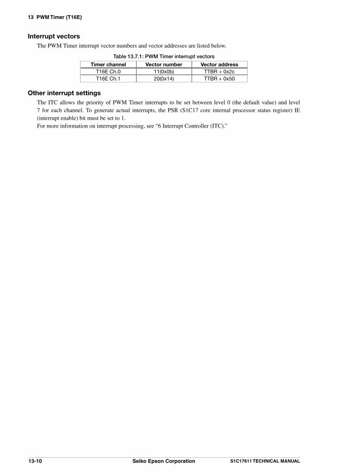
13 PWM Timer (T16E)
13-10 Seiko Epson Corporation S1C17611 TECHNICAL MANUAL
Interrupt vectors The PWM Timer interrupt vector numbers and vector addresses are listed below.
Table 13.7.1: PWM Timer interrupt vectors
Timer channel Vector number Vector addressT16E Ch.0 11(0x0b) TTBR + 0x2cT16E Ch.1 20(0x14) TTBR + 0x50
Other interrupt settings The ITC allows the priority of PWM Timer interrupts to be set between level 0 (the default value) and level
7 for each channel. To generate actual interrupts, the PSR (S1C17 core internal processor status register) IE (interrupt enable) bit must be set to 1.
For more information on interrupt processing, see “6 Interrupt Controller (ITC).”
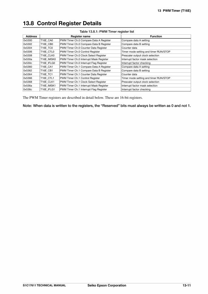
13 PWM Timer (T16E)
S1C17611 TECHNICAL MANUAL Seiko Epson Corporation 13-11
13.8 Control Register DetailsTable 13.8.1: PWM Timer register list
Address Register name Function0x5300 T16E_CA0 PWM Timer Ch.0 Compare Data A Register Compare data A setting0x5302 T16E_CB0 PWM Timer Ch.0 Compare Data B Register Compare data B setting0x5304 T16E_TC0 PWM Timer Ch.0 Counter Data Register Counter data
0x5306 T16E_CTL0 PWM Timer Ch.0 Control Register Timer mode setting and timer RUN/STOP0x5308 T16E_CLK0 PWM Timer Ch.0 Clock Select Register Prescaler output clock selection0x530a T16E_IMSK0 PWM Timer Ch.0 Interrupt Mask Register Interrupt factor mask selection0x530c T16E_IFLG0 PWM Timer Ch.0 Interrupt Flag Register Interrupt factor checking0x5360 T16E_CA1 PWM Timer Ch.1 Compare Data A Register Compare data A setting0x5362 T16E_CB1 PWM Timer Ch.1 Compare Data B Register Compare data B setting0x5364 T16E_TC1 PWM Timer Ch.1 Counter Data Register Counter data0x5366 T16E_CTL1 PWM Timer Ch.1 Control Register Timer mode setting and timer RUN/STOP0x5368 T16E_CLK1 PWM Timer Ch.1 Clock Select Register Prescaler output clock selection0x536a T16E_IMSK1 PWM Timer Ch.1 Interrupt Mask Register Interrupt factor mask selection0x536c T16E_IFLG1 PWM Timer Ch.1 Interrupt Flag Register Interrupt factor checking
The PWM Timer registers are described in detail below. These are 16-bit registers.
Note: When data is written to the registers, the “Reserved” bits must always be written as 0 and not 1.
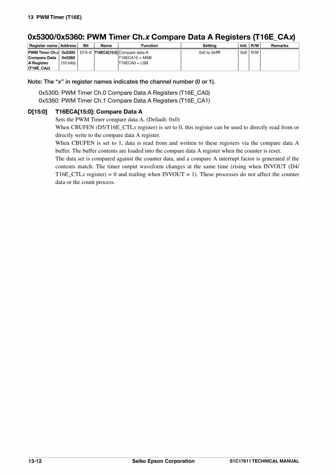
13 PWM Timer (T16E)
13-12 Seiko Epson Corporation S1C17611 TECHNICAL MANUAL
0x5300/0x5360: PWM Timer Ch.x Compare Data A Registers (T16E_CAx)Register name Address Bit Name Function Setting Init. R/W Remarks
PWM Timer Ch.x Compare Data A Register(T16E_CAx)
0x53000x5360(16 bits)
D15–0 T16ECA[15:0] Compare data AT16ECA15 = MSBT16ECA0 = LSB
0x0 to 0xffff 0x0 R/W
Note: The “x” in register names indicates the channel number (0 or 1).
0x5300: PWM Timer Ch.0 Compare Data A Registers (T16E_CA0) 0x5360: PWM Timer Ch.1 Compare Data A Registers (T16E_CA1)
D[15:0] T16ECA[15:0]: Compare Data A Sets the PWM Timer compare data A. (Default: 0x0) When CBUFEN (D5/T16E_CTLx register) is set to 0, this register can be used to directly read from or
directly write to the compare data A register. When CBUFEN is set to 1, data is read from and written to these registers via the compare data A
buffer. The buffer contents are loaded into the compare data A register when the counter is reset. The data set is compared against the counter data, and a compare A interrupt factor is generated if the
contents match. The timer output waveform changes at the same time (rising when INVOUT (D4/T16E_CTLx register) = 0 and trailing when INVOUT = 1). These processes do not affect the counter data or the count process.

13 PWM Timer (T16E)
S1C17611 TECHNICAL MANUAL Seiko Epson Corporation 13-13
0x5302/0x5362: PWM Timer Ch.x Compare Data B Registers (T16E_CBx)Register name Address Bit Name Function Setting Init. R/W Remarks
PWM Timer Ch.x Compare Data B Register(T16E_CBx)
0x53020x5362(16 bits)
D15–0 T16ECB[15:0] Compare data BT16ECB15 = MSBT16ECB0 = LSB
0x0 to 0xffff 0x0 R/W
Note: The “x” in register names indicates the channel number (0 or 1).
0x5302: PWM Timer Ch.0 Compare Data B Registers (T16E_CB0) 0x5362: PWM Timer Ch.1 Compare Data B Registers (T16E_CB1)
D[15:0] T16ECB[15:0]: Compare Data B Sets the PWM Timer compare data B. (Default: 0x0) When CBUFEN (D5/T16E_CTLx register) is set to 0, this register can be used to directly read from or
directly write to the compare data B register. When CBUFEN is set to 1, data is read from and written to these registers via the compare data B
buffer. The buffer contents are loaded into the compare data B register when the counter is reset. The data set is compared against the counter data, and a compare B interrupt factor is generated if the
contents match. The timer output waveform changes at the same time (rising when INVOUT (D4/T16E_CTLx register) = 0 and trailing when INVOUT = 1). The counter is reset to 0.
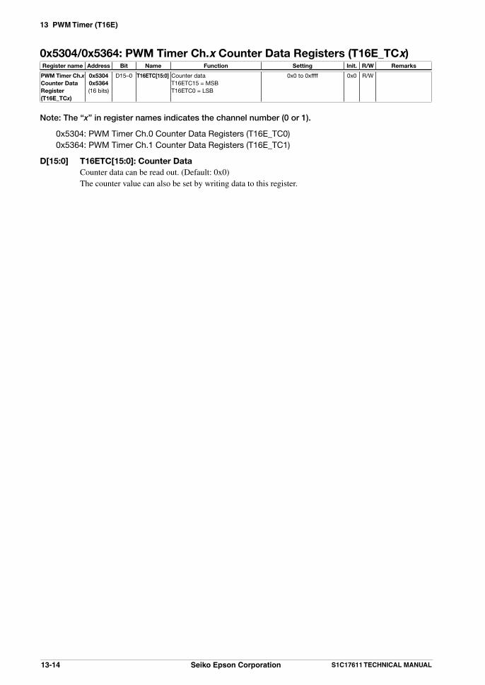
13 PWM Timer (T16E)
13-14 Seiko Epson Corporation S1C17611 TECHNICAL MANUAL
0x5304/0x5364: PWM Timer Ch.x Counter Data Registers (T16E_TCx)Register name Address Bit Name Function Setting Init. R/W Remarks
PWM Timer Ch.x Counter Data Register(T16E_TCx)
0x53040x5364(16 bits)
D15–0 T16ETC[15:0] Counter dataT16ETC15 = MSBT16ETC0 = LSB
0x0 to 0xffff 0x0 R/W
Note: The “x” in register names indicates the channel number (0 or 1).
0x5304: PWM Timer Ch.0 Counter Data Registers (T16E_TC0) 0x5364: PWM Timer Ch.1 Counter Data Registers (T16E_TC1)
D[15:0] T16ETC[15:0]: Counter Data Counter data can be read out. (Default: 0x0) The counter value can also be set by writing data to this register.

13 PWM Timer (T16E)
S1C17611 TECHNICAL MANUAL Seiko Epson Corporation 13-15
0x5306/0x5366: PWM Timer Ch.x Control Registers (T16E_CTLx)Register name Address Bit Name Function Setting Init. R/W Remarks
PWM Timer Ch.x Control Register(T16E_CTLx)
0x53060x5366(16 bits)
D15–9 – reserved – – – 0 when being read.D8 INITOL Initial output level 1 High 0 Low 0 R/WD7 – reserved – – – 0 when being read.D6 SELFM Fine mode select 1 Fine mode 0 Normal mode 0 R/WD5 CBUFEN Comparison buffer enable 1 Enable 0 Disable 0 R/WD4 INVOUT Inverse output 1 Invert 0 Normal 0 R/WD3 CLKSEL Input clock select 1 External 0 Internal 0 R/WD2 OUTEN Clock output enable 1 Enable 0 Disable 0 R/WD1 T16ERST Timer reset 1 Reset 0 Ignored 0 W 0 when being read.D0 T16ERUN Timer run/stop control 1 Run 0 Stop 0 R/W
Note: The “x” in register names indicates the channel number (0 or 1).
0x5306: PWM Timer Ch.0 Control Registers (T16E_CTL0) 0x5366: PWM Timer Ch.1 Control Registers (T16E_CTL1)
D[15:9] Reserved
D8 INITOL: Initial Output Level Bit Sets the timer output initial output level. 1 (R/W): TOUTx = High, TOUTNx = Low 0 (R/W): TOUTx = Low, TOUTNx = High (default)
The timer output pin switches to the initial output level set here when the clock output is switched off by writing 0 to OUTEN (D2). Note that this level will be inverted when INVOUT (D4) is 1.
D7 Reserved
D6 SELFM: Fine Mode Select Bit Sets the clock output to Fine mode. 1 (R/W): Fine mode 0 (R/W): Normal output (default)
When SELFM is set to 1, the clock output is set to Fine mode, and the output clock duty becomes adjustable in input clock half-cycle steps.
When SELFM is set to 0, normal clock output is used.
D5 CBUFEN: Comparison Buffer Enable Bit Permits and prevents writing to the compare data buffer. 1 (R/W): Permitted 0 (R/W): Prohibited (default)
When CBUFEN is set to 1, compare data is read and written via the compare data buffer. The buffer contents are loaded into the compare data register when the counter is reset by software or compare B signal.
When CBUFEN is set to 0, compare data is read and written directly to and from the compare data register.
D4 INVOUT: Inverse Output Control Bit Selects the timer output signal polarity. 1 (R/W): Inverted (TOUTx = active Low, TOUTNx = active High) 0 (R/W): Normal (TOUTx = active High, TOUTNx = active Low) (default)
Writing 1 to INVOUT generates a TOUTx output active Low signal (Off level = High). When INVOUT is 0, an active High signal (Off level = Low) is generated.
Writing 1 to this bit also inverts the initial output level set by INITOL (D8). The signal level above is inverted for TOUTNx output.

13 PWM Timer (T16E)
13-16 Seiko Epson Corporation S1C17611 TECHNICAL MANUAL
D3 CLKSEL: Input Clock Select Bit Selects the timer input clock. 1 (R/W): External clock 0 (R/W): Internal clock (default)
Writing 0 to CLKSEL selects the internal clock (Prescaler output) for the timer input clock, writing 1 selects the external clock (a clock input via the EXCL3 (P06) pin for Ch.0 and the EXCL4 (P07) pin for Ch.1) and acts it as an event counter.
D2 OUTEN: Clock Output Enable Bit Controls the TOUTx/TOUTNx signal (timer output clock) output. 1 (R/W): Permitted 0 (R/W): Prohibited (default)
Writing 1 to OUTEN outputs the TOUTx/TOUTNx signal from the corresponding output pin. Ch.0: TOUT3 output → TOUT3 (P12, P15) pin, TOUTN3 output → TOUTN3 (P13) pin Ch.1: TOUT4 output → TOUT4 (P05, P11) pin, TOUTN4 output → TOUTN4 (P11) pin
Writing 0 to OUTEN stops the output, and switches to the Off level corresponding to the settings for INVOUT (D4). The above pins must be set to TOUTx/TOUTNx output using the port function selection register before outputting the TOUTx/TOUTNx signals.
D1 T16ERST: Timer Reset Bit Resets the counter. 1 (W): Reset 0 (W): Disabled 0 (R): Normally 0 when read out (default)
Writing 1 to T16ERST resets the PWM Timer counter.
D0 T16ERUN: Timer Run/Stop Control Bit Controls the timer Run/Stop. 1 (R/W): Run 0 (R/W): Stop (default)
The PWM Timer starts the count when T16ERUN is written as 1 and stops when written as 0. The counter data is retained when stopped until the subsequent reset or run. Counting can be resumed when switched from Stop to Run from the data retained.

13 PWM Timer (T16E)
S1C17611 TECHNICAL MANUAL Seiko Epson Corporation 13-17
0x5308/0x5368: PWM Timer Ch.x Input Clock Select Registers (T16E_CLKx)Register name Address Bit Name Function Setting Init. R/W Remarks
PWM Timer Ch.x Input Clock Select Register(T16E_CLKx)
0x53080x5368(16 bits)
D15–4 – reserved – – – 0 when being read.D3–0 T16EDF[3:0] Timer input clock select
(Prescaler output clock)T16EDF[3:0] Clock 0x0 R/W
0xf0xe0xd0xc0xb0xa0x90x80x70x60x50x40x30x20x10x0
reservedPCLK•1/16384PCLK•1/8192PCLK•1/4096PCLK•1/2048PCLK•1/1024PCLK•1/512PCLK•1/256PCLK•1/128PCLK•1/64PCLK•1/32PCLK•1/16PCLK•1/8PCLK•1/4PCLK•1/2PCLK•1/1
Note: The “x” in register names indicates the channel number (0 or 1).
0x5308: PWM Timer Ch.0 Input Clock Select Registers (T16E_CLK0) 0x5368: PWM Timer Ch.1 Input Clock Select Registers (T16E_CLK1)
D[15:4] Reserved
D[3:0] T16EDF[3:0]: Timer Input Clock Select Bits Select the PWM Timer count clock from the 15 different prescaler output clocks.
Table 13.8.2: Count clock selection
T16EDF[3:0] Prescaler output clock T16EDF[3:0] Prescaler output clock0xf Reserved 0x7 PCLK•1/1280xe PCLK•1/16384 0x6 PCLK•1/640xd PCLK•1/8192 0x5 PCLK•1/320xc PCLK•1/4096 0x4 PCLK•1/160xb PCLK•1/2048 0x3 PCLK•1/80xa PCLK•1/1024 0x2 PCLK•1/40x9 PCLK•1/512 0x1 PCLK•1/20x8 PCLK•1/256 0x0 PCLK•1/1
(Default: 0x0)
Note: Make sure the PWM Timer count is halted before changing count clock settings.

13 PWM Timer (T16E)
13-18 Seiko Epson Corporation S1C17611 TECHNICAL MANUAL
0x530a/0x536a: PWM Timer Ch.x Interrupt Mask Registers (T16E_IMSKx)Register name Address Bit Name Function Setting Init. R/W Remarks
PWM Timer Ch.x Interrupt Mask Register(T16E_IMSKx)
0x530a0x536a(16 bits)
D15–2 – reserved – – – 0 when being read.
D1 CBIE Compare B interrupt enable 1 Enable 0 Disable 0 R/WD0 CAIE Compare A interrupt enable 1 Enable 0 Disable 0 R/W
Note: The “x” in register names indicates the channel number (0 or 1).
0x530a: PWM Timer Ch.0 Interrupt Mask Registers (T16E_IMSK0) 0x536a: PWM Timer Ch.1 Interrupt Mask Registers (T16E_IMSK1)
D[15:2] Reserved
D1 CBIE: Compare B Interrupt Enable Bit Permits or prohibits compare B match interrupts. 1 (R/W): Interrupt permitted 0 (R/W): Interrupt prohibited (default)
Setting CBIE to 1 permits compare B interrupt requests to the ITC. Setting it to 0 prohibits interrupts.
D0 CAIE: Compare A Interrupt Enable Bit Permits or prohibits compare A match interrupts. 1 (R/W): Interrupt permitted 0 (R/W): Interrupt prohibited (default)
Setting CAIE to 1 permits compare A interrupt requests to the ITC. Setting it to 0 prohibits interrupts.
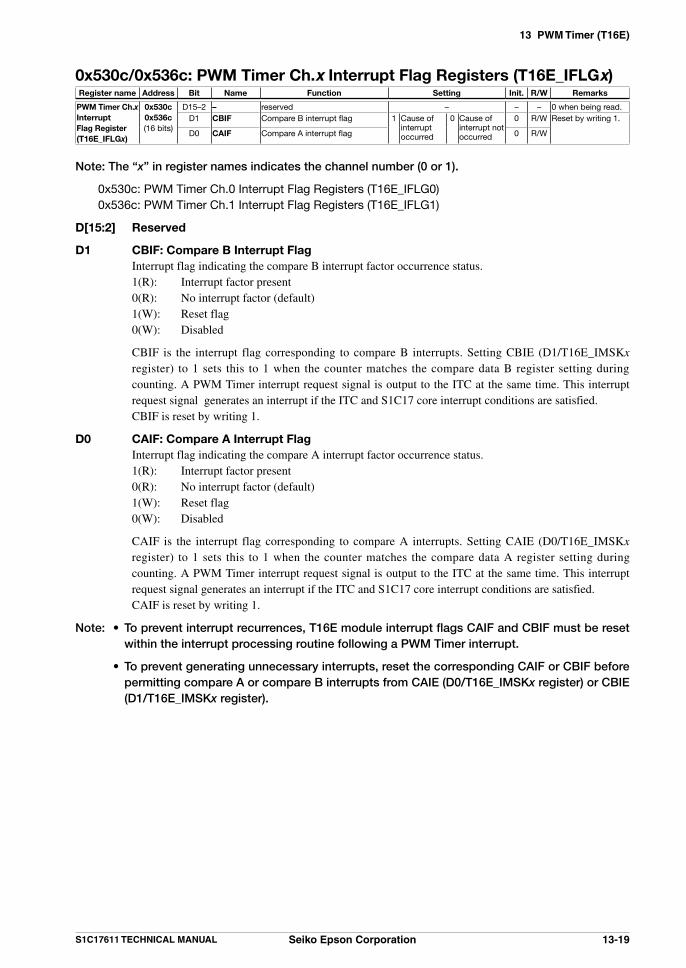
13 PWM Timer (T16E)
S1C17611 TECHNICAL MANUAL Seiko Epson Corporation 13-19
0x530c/0x536c: PWM Timer Ch.x Interrupt Flag Registers (T16E_IFLGx)Register name Address Bit Name Function Setting Init. R/W Remarks
PWM Timer Ch.x Interrupt Flag Register(T16E_IFLGx)
0x530c0x536c(16 bits)
D15–2 – reserved – – – 0 when being read.D1 CBIF Compare B interrupt flag 1 Cause of
interrupt occurred
0 Cause of interrupt not occurred
0 R/W Reset by writing 1.
D0 CAIF Compare A interrupt flag 0 R/W
Note: The “x” in register names indicates the channel number (0 or 1).
0x530c: PWM Timer Ch.0 Interrupt Flag Registers (T16E_IFLG0) 0x536c: PWM Timer Ch.1 Interrupt Flag Registers (T16E_IFLG1)
D[15:2] Reserved
D1 CBIF: Compare B Interrupt Flag Interrupt flag indicating the compare B interrupt factor occurrence status. 1(R): Interrupt factor present 0(R): No interrupt factor (default) 1(W): Reset flag 0(W): Disabled
CBIF is the interrupt flag corresponding to compare B interrupts. Setting CBIE (D1/T16E_IMSKx register) to 1 sets this to 1 when the counter matches the compare data B register setting during counting. A PWM Timer interrupt request signal is output to the ITC at the same time. This interrupt request signal generates an interrupt if the ITC and S1C17 core interrupt conditions are satisfied.
CBIF is reset by writing 1.
D0 CAIF: Compare A Interrupt Flag Interrupt flag indicating the compare A interrupt factor occurrence status. 1(R): Interrupt factor present 0(R): No interrupt factor (default) 1(W): Reset flag 0(W): Disabled
CAIF is the interrupt flag corresponding to compare A interrupts. Setting CAIE (D0/T16E_IMSKx register) to 1 sets this to 1 when the counter matches the compare data A register setting during counting. A PWM Timer interrupt request signal is output to the ITC at the same time. This interrupt request signal generates an interrupt if the ITC and S1C17 core interrupt conditions are satisfied.
CAIF is reset by writing 1.
Note: • To prevent interrupt recurrences, T16E module interrupt flags CAIF and CBIF must be reset within the interrupt processing routine following a PWM Timer interrupt.
• To prevent generating unnecessary interrupts, reset the corresponding CAIF or CBIF before permitting compare A or compare B interrupts from CAIE (D0/T16E_IMSKx register) or CBIE (D1/T16E_IMSKx register).

13 PWM Timer (T16E)
13-20 Seiko Epson Corporation S1C17611 TECHNICAL MANUAL
13.9 Precautions• The prescaler must run before operating the PWM Timer.
• Make sure the PWM Timer count is halted before changing count clock settings.
• Compare data should be set with A ≥ 0 and B ≥ 1 when using the timer output. The minimum settings are A = 0 and B = 1, and the timer output cycle is half the input clock.
• Setting compare data with A > B (A > B x 2 for Fine mode) generates a compare B match signal only. It does not generate a compare A match signal. In this case, the timer output is fixed at Low (High when INVOUT = 1).
• To prevent interrupt recurrences, the T16E module interrupt flags CAIF (D0/T16E_IFLGx register) and CBIF (D1/T16E_IFLGx register) must be reset within the interrupt processing routine following a PWM Timer interrupt.
• To prevent generating unnecessary interrupts, reset the corresponding CAIF (D0/T16E_IFLGx register) or CBIF (D1/T16E_IFLGx register) before permitting compare A or compare B interrupts from CAIE (D0/T16E_IMSKx register) or CBIE (D1/T16E_IMSKx register).

14 8-bit OSC1 Timer (T8OSC1)
S1C17611 TECHNICAL MANUAL Seiko Epson Corporation 14-1
14 8-bit OSC1 Timer (T8OSC1)
14.1 8-bit OSC1 Timer OverviewThe S1C17611 incorporates an 1-channel 8-bit OSC1 timer that uses the OSC1 clock as its oscillation source.Figure 14.1.1 illustrates the 8-bit OSC1 timer configuration.
Compare data registerT8OSC1_CMP
OSC1•1/1 to 1/32
Inte
rnal
dat
a b
us
Compare match interrupt requestTo ITC
Up counterT8OSC1_CNT
Countcontrolcircuit
Interruptcontrol circuit
Comparator
Interrupt enableT8OIE
8-bit OSC1 timerOSC
OSC1 oscillator /division circuit Gate
Division ratio selection
PWM outputP02/TOUT5
PWM duty data register T8OSC1_DUTY
Comparator
RUN/STOP control
Timer reset
Count modeselection
T8ORUN
T8ORST
T8ORMD
Comparematchsignal
Duty matchsignal
Figure 14.1.1: 8-bit OSC1 timer configuration
The 8-bit OSC1 timer includes an 8-bit up-counter (T8OSC1_CNT register), an 8-bit compare data register (T8OSC1_CMP register), and an 8-bit PWM duty data register (T8OSC1_DUTY register).
The 8-bit counter can be reset to 0 by software and counts up using the OSC1 division clock (OSC1•1/1 to OSC1•1/32). The count value can be read by software.
The compare data and PWM duty registers store the data used for comparisons against up-counter contents.If the counter values match the contents of each data register, the comparator outputs a signal to control the interrupts and the PWM output signal. The compare data register can be used to set the interrupt generating and PWM output clock frequencies. The PWM duty data register can be used to set the PWM output clock duty ratio.

14 8-bit OSC1 Timer (T8OSC1)
14-2 Seiko Epson Corporation S1C17611 TECHNICAL MANUAL
14.2 8-bit OSC1 Timer Count ModeThe 8-bit OSC1 timer features two count modes: Repeat mode and One-shot mode. These modes are selected using the T8ORMD bit (D1/T8OSC1_CTL register).
* T8ORMD: Count Mode Select Bit in the 8-bit OSC1 Timer Control (T8OSC1_CTL) Register (D1/0x50c0)
Repeat mode (T8ORMD = 0, default) Setting T8ORMD to 0 sets the 8-bit OSC1 timer to Repeat mode. In this mode, once the count starts, the 8-bit OSC1 timer continues running until stopped by the application
program. If the counter matches the compare data, the timer resets the counter and continues counting. The interrupt signal is output at the same time. The 8-bit OSC1 timer should be set to this mode to generate periodic interrupts at desired intervals or to perform PWM output.
One-shot mode (T8ORMD = 1) Setting T8ORMD to 1 sets the 8-bit OSC1 timer to One-shot mode. In this mode, the 8-bit OSC1 timer stops automatically as soon as the counter matches the compare data. This means only one interrupt can be generated after the timer starts. Note that the timer resets the counter, then
stops after a complete match has occurred. The 8-bit OSC1 timer should be set to this mode to set a specific wait time.
Note: • Make sure the 8-bit OSC1 timer count is halted before changing count mode settings. • If count operation is activated while the count mode is set to one-shot mode, and the CPU
enters halt state, the counter does not stop even when a compare match occurs, disabling one-shot operation.

14 8-bit OSC1 Timer (T8OSC1)
S1C17611 TECHNICAL MANUAL Seiko Epson Corporation 14-3
14.3 Count ClockThe 8-bit OSC1 timer uses the OSC1 division clock output by the OSC module as the count clock. The OSC module generates 6 different clocks by dividing the OSC1 clock into 1/1 to 1/32 divisions. One of these is selected by T8O1CK[2:0] (D[3:1]/OSC_T8OSC1 register).
* T8O1CK[2:0]: T8OSC1 Clock Division Ratio Select Bits in the T8OSC1 Clock Control (OSC_T8OSC1) Register (D[3:1]/0x5065)
Table 14.3.1: Count clock selection
T8O1CK[2:0] Division ratio0x7 to 0x6 Reserved
0x5 OSC1•1/320x4 OSC1•1/160x3 OSC1•1/80x2 OSC1•1/40x1 OSC1•1/20x0 OSC1•1/1
(Default: 0x0)
The clock feed to the 8-bit OSC1 timer is controlled using T8O1CE (D0/OSC_T8OSC1 register). The T8O1CE default setting is 0, which stops the clock feed. Setting T8O1CE to 1 sends the clock generated as above to the 8-bit OSC1 timer. If 8-bit OSC1 timer operation is not required, the clock feed should be stopped to reduce power consumption.
* T8O1CE: T8OSC1 Clock Enable Bit in the T8OSC1 Clock Control (OSC_T8OSC1) Register (D0/0x5065)
Note: Make sure the 8-bit OSC1 timer count is halted before changing count clock settings.
For detailed information on clock control, refer to “7 Oscillator Circuit (OSC).”

14 8-bit OSC1 Timer (T8OSC1)
14-4 Seiko Epson Corporation S1C17611 TECHNICAL MANUAL
14.4 Resetting 8-bit OSC1 TimerReset the 8-bit OSC1 Timer by writing 1 to the T8ORST bit (D4/T8OSC1_CTL register). This clears the counter 0.
* T8ORST: Timer Reset Bit in the 8-bit OSC1 Timer Control (T8OSC1_CTL) Register (D4/0x50c0)
Normally, the counter should be reset by writing 1 to this bit before starting the count.The counter is reset by hardware if the counter matches compare data after the count starts.

14 8-bit OSC1 Timer (T8OSC1)
S1C17611 TECHNICAL MANUAL Seiko Epson Corporation 14-5
14.5 Compare Data SettingsCompare data is written to T8OCMP[7:0] (D[7:0]/T8OSC1_CMP register).
* T8OCMP[7:0]: Compare Data Bits in the 8-bit OSC1 Timer Compare Data (T8OSC1_CMP) Register (D[7:0]/0x50c2)
After initial resetting, the compare data register is set to 0x0.
The timer compares the count data against the compare data register and generates a compare match signal as well as resets the counter if the values are equal. This compare match signal can generate an interrupt.The compare match cycle can be calculated as follows:
CMP + 1 Compare match interval = ————— [s] clk_in
clk_in Compare match cycle = ————— [Hz] CMP + 1
CMP: Compare data (T8OSC1_CMP register value) clk_in: 8-bit OSC1 timer count clock frequency
When the 8-bit OSC1 timer is used to generate a PWM signal, the compare data determines the frequency of the output signal. (For a discussion of PWM output, refer to Section 14.8.)

14 8-bit OSC1 Timer (T8OSC1)
14-6 Seiko Epson Corporation S1C17611 TECHNICAL MANUAL
14.6 8-bit OSC1 Timer RUN/STOP ControlSet the following items before starting the 8-bit OSC1 timer.(1) Set the count mode (One-shot or Repeat). See Section 14.2.(2) Select the operation clock. See Section 14.3.(3) If using interrupts, set the interrupt level and permit interrupts for the 8-bit OSC1 timer. See Section 14.7.(4) Reset the timer. See Section 14.4.(5) Set the compare data. See Section 14.5.(6) To output PWM signals, set the PWM duty data. See Section 14.8.
The 8-bit OSC1 timer includes T8ORUN (D0/T8OSC1_CTL register) to control Run/Stop.
* T8ORUN: Timer Run/Stop Control Bit in the 8-bit OSC1 Timer Control (T8OSC1_CTL) Register (D0/0x50c0)
The timer starts counting when T8ORUN is written as 1. Writing 0 to T8ORUN prevents clock input and stops the count.This control does not affect the counter data. The counter data is retained even when the count is halted, allowing resumption of the count from that data.If T8ORUN and T8ORST are written as 1 simultaneously, the timer starts counting after the reset.
If the counter matches the compare data register setting during counting, a compare match signal is output and a compare interrupt factor generated. The counter is reset to 0 at the same time. If interrupts are permitted, an interrupt request is sent to the interrupt controller (ITC).If One-shot mode is set, the timer stops the count.If Repeat mode is set, the timer continues to count from 0.
T8ORUN
T8ORST
T8OCMP
Input clock
T8OCNT
Reset Reset &compare match interrupt
Reset &compare match interrupt
0 1 2 3 4 5 0 1 2 3 4 5 0 1
0x5
T8ORUN
T8ORST
T8OCMP
Input clock
T8OCNT
Reset Reset &compare match interrupt
0 1 2 3 4 5 0
0x5
One-shot mode
Repeat mode
Figure 14.6.1: Basic counter operation timing

14 8-bit OSC1 Timer (T8OSC1)
S1C17611 TECHNICAL MANUAL Seiko Epson Corporation 14-7
14.7 8-bit OSC1 Timer InterruptsThe T8OSC1 module outputs an interrupt request to the interrupt controller (ITC) by compare match.
Compare match interrupt This interrupt request is generated when the counter matches the compare data register setting during counting.
It sets the interrupt flag T8OIF (D0/T8OSC1_IFLG register) within the T8OSC1 module to 1.
* T8OIF: 8-bit OSC1 Timer Interrupt Flag in the 8-bit OSC1 Timer Interrupt Flag (T8OSC1_IFLG) Register (D0/0x50c4)
To use this interrupt, set T8OIE (D0/T8OSC1_IMSK register) to 1. If T8OIE is set to 0 (default), T8OIF is not set to 1, and the interrupt request for this factor is not sent to the ITC.
* T8OIE: 8-bit OSC1 Timer Interrupt Enable Bit in the 8-bit OSC1 Timer Interrupt Mask (T8OSC1_IMSK) Register (D0/0x50c3)
If T8OIF is set to 1, the T8OSC1 module outputs an interrupt request to the ITC. An interrupt is generated if the ITC and S1C17 core interrupt conditions are satisfied.
Note: • To prevent interrupt recurrences, the T8OSC1 module interrupt flag T8OIF must be reset within the interrupt handler routine following an 8-bit OSC1 timer interrupt.
• To prevent generating unnecessary interrupts, reset the corresponding T8OIF before permitting compare 8-bit OSC1 interrupts by T8OIE.
Interrupt vectors The 8-bit OSC1 timer interrupt vector numbers and vector addresses are listed below.
Vector number: 8 (0x08) Vector address: TTBR + 0x20
Other interrupt settings The ITC allows the priority of 8-bit OSC1 timer interrupts to be set between level 0 (the default value) and level 7.
To generate actual interrupts, the PSR (S1C17 core internal processor status register) IE (interrupt enable) bit must be set to 1.
For more information on interrupt processing, see “6 Interrupt Controller (ITC).”

14 8-bit OSC1 Timer (T8OSC1)
14-8 Seiko Epson Corporation S1C17611 TECHNICAL MANUAL
14.8 PWM outputThe 8-bit OSC1 timer can generate a PWM signal in accordance with the compare data and PWM duty data settings and output it from the TOUT5 (P02) pin.
Output pin setting The PWM output pin (TOUT5) also acts as a pin (P02) for a general-purpose input/output port. In the default
state, this pin is set as a general-purpose input/output port pin. To use it as a PWM output pin, change the function by setting the value 1 in the P02MUX (D5-4/P0_PMUX register).
* P02MUX: P02 Port Function Select Bit in the P0 Port Function Select (P0_PMUX) Register (D5-4/0x52a0)
PWM waveform control The PWM waveform frequency can be set by the compare data register (0x50c2) (see Section 14.5). The duty
ratio can be adjusted by the PWM duty data register (0x50c5). The timer outputs a Low level signal until the counter value matches the value of the PWM duty data register.
When the counter value exceeds the value of the PWM duty data, the output pin changes to High. Once the counter counts up to the compare data register value, the counter is reset and the output pin returns to Low.
Figure 14.8.1 shows the output waveform.
Input clock
T8ORUN
Counter value
Duty match signal
Compare match signal
TOUT5 output
1 2 3 4 5 00 1 2 3 4 5 0 1 2 3 2 34 5 0 1
(when T8OSC1_DUTY = 3 and T8OSC1_CMP = 5)
Figure 14.8.1 PWM output waveform
Precautions(1) When using the timer output, set the following: PWM duty data ≥ 0, compare data ≥ 1. The minimum
setting value is 0 for PWM duty data and 1 for compare data. The timer output cycle is 1/2 of the input clock.
(2) When the PWM duty data is set greater than the compare data, only the compare match signal will be generated. No duty match signal will be generated. In that case, the TOUT5 output is fixed to Low.
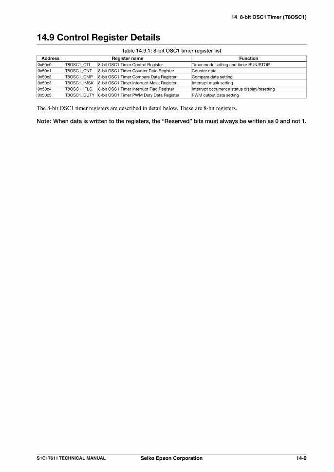
14 8-bit OSC1 Timer (T8OSC1)
S1C17611 TECHNICAL MANUAL Seiko Epson Corporation 14-9
14.9 Control Register DetailsTable 14.9.1: 8-bit OSC1 timer register list
Address Register name Function0x50c0 T8OSC1_CTL 8-bit OSC1 Timer Control Register Timer mode setting and timer RUN/STOP0x50c1 T8OSC1_CNT 8-bit OSC1 Timer Counter Data Register Counter data0x50c2 T8OSC1_CMP 8-bit OSC1 Timer Compare Data Register Compare data setting
0x50c3 T8OSC1_IMSK 8-bit OSC1 Timer Interrupt Mask Register Interrupt mask setting0x50c4 T8OSC1_IFLG 8-bit OSC1 Timer Interrupt Flag Register Interrupt occurrence status display/resetting0x50c5 T8OSC1_DUTY 8-bit OSC1 Timer PWM Duty Data Register PWM output data setting
The 8-bit OSC1 timer registers are described in detail below. These are 8-bit registers.
Note: When data is written to the registers, the “Reserved” bits must always be written as 0 and not 1.
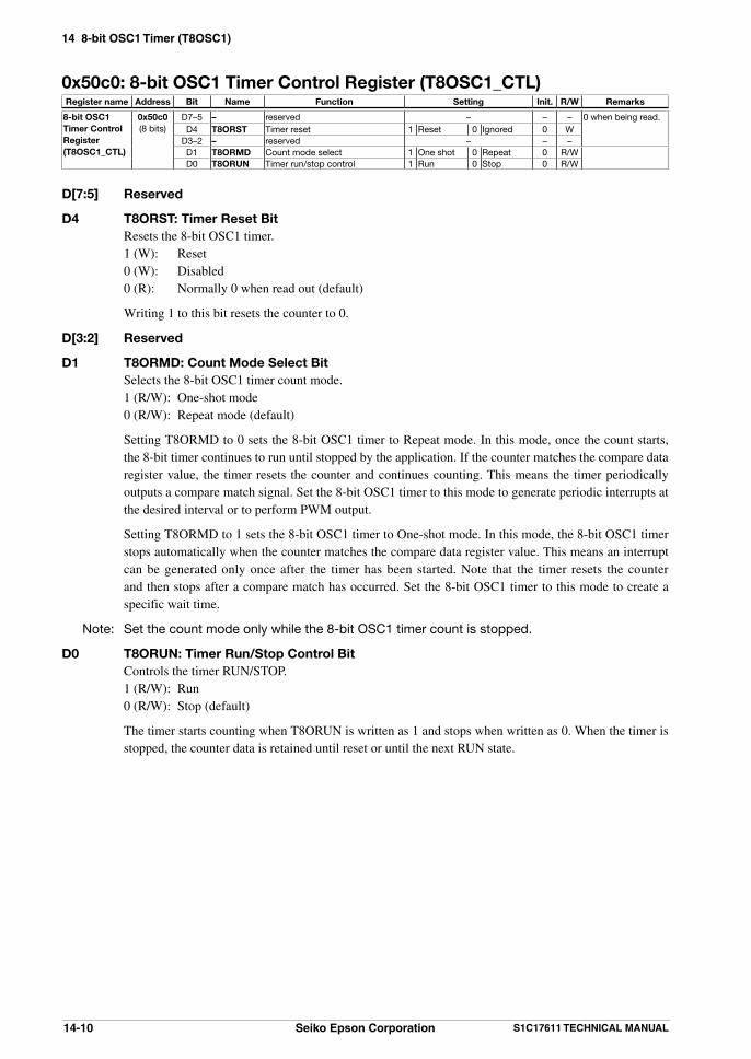
14 8-bit OSC1 Timer (T8OSC1)
14-10 Seiko Epson Corporation S1C17611 TECHNICAL MANUAL
0x50c0: 8-bit OSC1 Timer Control Register (T8OSC1_CTL)Register name Address Bit Name Function Setting Init. R/W Remarks
8-bit OSC1 Timer Control Register(T8OSC1_CTL)
0x50c0(8 bits)
D7–5 – reserved – – – 0 when being read.D4 T8ORST Timer reset 1 Reset 0 Ignored 0 W
D3–2 – reserved – – –D1 T8ORMD Count mode select 1 One shot 0 Repeat 0 R/WD0 T8ORUN Timer run/stop control 1 Run 0 Stop 0 R/W
D[7:5] Reserved
D4 T8ORST: Timer Reset Bit Resets the 8-bit OSC1 timer. 1 (W): Reset 0 (W): Disabled 0 (R): Normally 0 when read out (default)
Writing 1 to this bit resets the counter to 0.
D[3:2] Reserved
D1 T8ORMD: Count Mode Select Bit Selects the 8-bit OSC1 timer count mode. 1 (R/W): One-shot mode 0 (R/W): Repeat mode (default)
Setting T8ORMD to 0 sets the 8-bit OSC1 timer to Repeat mode. In this mode, once the count starts, the 8-bit timer continues to run until stopped by the application. If the counter matches the compare data register value, the timer resets the counter and continues counting. This means the timer periodically outputs a compare match signal. Set the 8-bit OSC1 timer to this mode to generate periodic interrupts at the desired interval or to perform PWM output.
Setting T8ORMD to 1 sets the 8-bit OSC1 timer to One-shot mode. In this mode, the 8-bit OSC1 timer stops automatically when the counter matches the compare data register value. This means an interrupt can be generated only once after the timer has been started. Note that the timer resets the counter and then stops after a compare match has occurred. Set the 8-bit OSC1 timer to this mode to create a specific wait time.
Note: Set the count mode only while the 8-bit OSC1 timer count is stopped.
D0 T8ORUN: Timer Run/Stop Control Bit Controls the timer RUN/STOP. 1 (R/W): Run 0 (R/W): Stop (default)
The timer starts counting when T8ORUN is written as 1 and stops when written as 0. When the timer is stopped, the counter data is retained until reset or until the next RUN state.

14 8-bit OSC1 Timer (T8OSC1)
S1C17611 TECHNICAL MANUAL Seiko Epson Corporation 14-11
0x50c1: 8-bit OSC1 Timer Counter Data Register (T8OSC1_CNT)Register name Address Bit Name Function Setting Init. R/W Remarks
8-bit OSC1 Timer Counter Data Register(T8OSC1_CNT)
0x50c1(8 bits)
D7–0 T8OCNT[7:0] Timer counter dataT8OCNT7 = MSBT8OCNT0 = LSB
0x0 to 0xff 0x0 R
D[7:0] T8OCNT[7:0]: Counter Data Reads out the counter data. (Default: 0x0) This register is read-only and cannot be written to.
Note: The correct counter value may not be read out (reading is unstable) if the register is read while counting is underway.
Obtain the counter value by one of the following methods: • Read the counter value while the counter is halted. • Read the counter twice in succession. Treat the value as valid if the values read are identical.

14 8-bit OSC1 Timer (T8OSC1)
14-12 Seiko Epson Corporation S1C17611 TECHNICAL MANUAL
0x50c2: 8-bit OSC1 Timer Compare Data Register (T8OSC1_CMP)Register name Address Bit Name Function Setting Init. R/W Remarks
8-bit OSC1 Timer Compare Data Register(T8OSC1_CMP)
0x50c2(8 bits)
D7–0 T8OCMP[7:0] Compare dataT8OCMP7 = MSBT8OCMP0 = LSB
0x0 to 0xff 0x0 R/W
D[7:0] T8OCMP[7:0]: Compare Data Sets the 8-bit OSC1 timer compare data. (Default: 0x0) The data set is compared against the counter data, and a compare match interrupt factor is generated if
the contents match. And the counter is reset to 0.

14 8-bit OSC1 Timer (T8OSC1)
S1C17611 TECHNICAL MANUAL Seiko Epson Corporation 14-13
0x50c3: 8-bit OSC1 Timer Interrupt Mask Register (T8OSC1_IMSK)Register name Address Bit Name Function Setting Init. R/W Remarks
8-bit OSC1 Timer Interrupt Mask Register(T8OSC1_IMSK)
0x50c3(8 bits)
D7–1 – reserved – – – 0 when being read.D0 T8OIE 8-bit OSC1 timer interrupt enable 1 Enable 0 Disable 0 R/W
D[7:1] Reserved
D0 T8OIE: 8-bit OSC1 Timer Interrupt Enable Bit Permits or prohibits compare match interrupts. 1 (R/W): Interrupt permitted 0 (R/W): Interrupt prohibited (default)
Setting T8OIE to 1 permits 8-bit OSC1 timer interrupt requests to the ITC. Setting it to 0 prohibits interrupts.
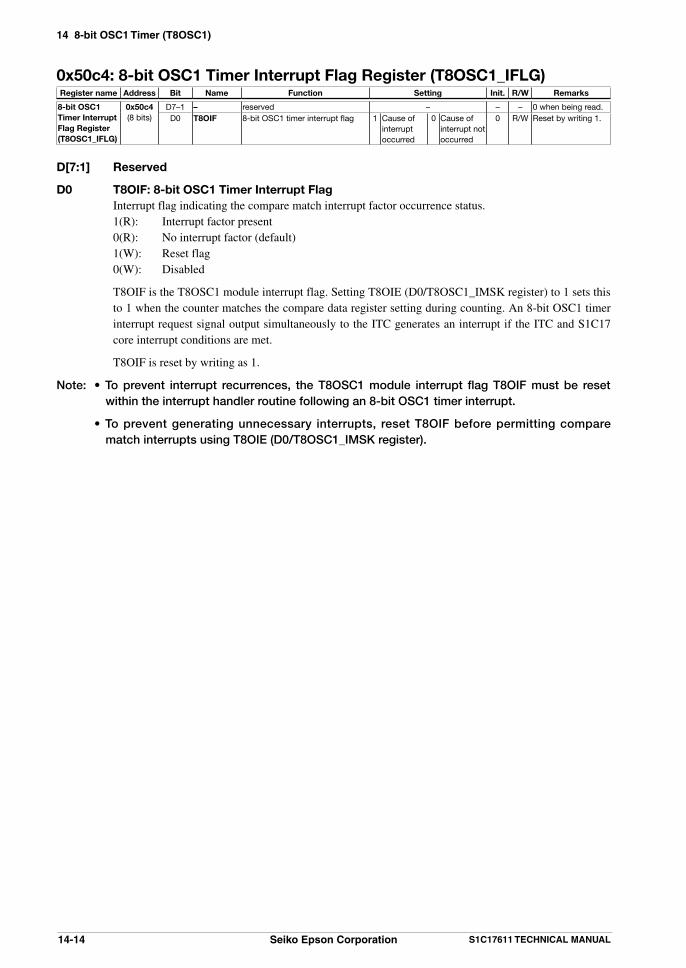
14 8-bit OSC1 Timer (T8OSC1)
14-14 Seiko Epson Corporation S1C17611 TECHNICAL MANUAL
0x50c4: 8-bit OSC1 Timer Interrupt Flag Register (T8OSC1_IFLG)Register name Address Bit Name Function Setting Init. R/W Remarks
8-bit OSC1 Timer Interrupt Flag Register(T8OSC1_IFLG)
0x50c4(8 bits)
D7–1 – reserved – – – 0 when being read.D0 T8OIF 8-bit OSC1 timer interrupt flag 1 Cause of
interrupt occurred
0 Cause of interrupt not occurred
0 R/W Reset by writing 1.
D[7:1] Reserved
D0 T8OIF: 8-bit OSC1 Timer Interrupt Flag Interrupt flag indicating the compare match interrupt factor occurrence status. 1(R): Interrupt factor present 0(R): No interrupt factor (default) 1(W): Reset flag 0(W): Disabled
T8OIF is the T8OSC1 module interrupt flag. Setting T8OIE (D0/T8OSC1_IMSK register) to 1 sets this to 1 when the counter matches the compare data register setting during counting. An 8-bit OSC1 timer interrupt request signal output simultaneously to the ITC generates an interrupt if the ITC and S1C17 core interrupt conditions are met.
T8OIF is reset by writing as 1.
Note: • To prevent interrupt recurrences, the T8OSC1 module interrupt flag T8OIF must be reset within the interrupt handler routine following an 8-bit OSC1 timer interrupt.
• To prevent generating unnecessary interrupts, reset T8OIF before permitting compare match interrupts using T8OIE (D0/T8OSC1_IMSK register).

14 8-bit OSC1 Timer (T8OSC1)
S1C17611 TECHNICAL MANUAL Seiko Epson Corporation 14-15
0x50c5: 8-bit OSC1 Timer PWM Duty Data Register (T8OSC1_DUTY)Register name Address Bit Name Function Setting Init. R/W Remarks
8-bit OSC1 Timer PWM Duty Data Register(T8OSC1_DUTY)
0x50c5(8 bits)
D7–0 T8ODTY[7:0] PWM output duty dataT8ODTY7 = MSBT8ODTY0 = LSB
0x0 to 0xff 0x0 R/W
D[7:0] T8ODTY[7:0]: PWM Output Duty Data Sets the data that determines the duty ratio of PWM waveform. (default: 0x0) The set data is compared against the counter data. If the contents match, the timer output waveform
rises. If the counter data matches the compare data, the timer output waveform falls. These processes do not affect the counter data or count process.

14 8-bit OSC1 Timer (T8OSC1)
14-16 Seiko Epson Corporation S1C17611 TECHNICAL MANUAL
14.10 Precautions• The 8-bit OSC1 timer clock must be output from the OSC module before the 8-bit OSC1 timer begins running.
• Set the count clock and count mode only while the 8-bit OSC1 timer count is stopped.
• To prevent interrupt recurrences, the T8OSC1 module interrupt flag T8OIF (D0/T8OSC1_IFLG register) must be reset within the interrupt handler routine following an 8-bit OSC1 timer interrupt.
• To prevent generating unnecessary interrupts, reset T8OIF (D0/T8OSC1_IFLG register) before permitting compare match interrupts using T8OIE (D0/T8OSC1_IMSK register).
• The correct counter value may not be read out (reading is unstable) if the counter data register is read while counting is underway.
To obtain the counter value, read the counter data register while the counter is halted or read the counter data register twice in succession. Treat the value as valid if the values read are identical.
• When using the PWM output, set the following: PWM duty data ≥ 0, compare data ≥ 1. The minimum setting value is 0 for PWM duty data and 1 for compare data. The timer output cycle is 1/2 of the input clock.
• When the PWM duty data is set greater than the compare data, only the compare match signal is generated. No duty match signal is generated. In that case, the TOUT5 output is fixed to Low.
• Make sure the 8-bit OSC1 timer count is halted before changing count mode settings.
• If count operation is activated while the count mode is set to one-shot mode, and the CPU enters halt state, the counter does not stop even when a compare match occurs, disabling one-shot operation.

15 Clock Timer (CT)
S1C17611 TECHNICAL MANUAL Seiko Epson Corporation 15-1
15 Clock Timer (CT)
15.1 Clock Timer OverviewThe S1C17611 incorporates an 1-channel clock timer that uses the OSC1 clock as its oscillation source.The clock timer consists of an 8-bit binary counter that uses the 256 Hz signal divided from the OSC1 clock as the input clock and allows data for each bit (128 Hz to 1 Hz) to be read out by software.The clock timer can also generate interrupts using the 32 Hz, 8 Hz, 2 Hz, and 1 Hz signals.This clock timer is normally used for various timing functions, such as clocks.Figure 15.1.1 illustrates the clock timer configuration.
256Hz
Inte
rnal
dat
a b
us
Clock timer interrupt requestTo ITC
128Hz
64Hz
32Hz
16Hz
8Hz
4Hz
2Hz
1Hz
Countcontrolcircuit
Interrupt controlcircuit
RUN/STOPcontrol
Interrupt enable
CTRUN
CTIE32CTIE8CTIE2CTIE1
Timer reset CTRST
CT_CNTD0 D1 D2 D3 D4 D5 D6 D7
Clock timerOSC
OSC1 oscillator/division circuit
Figure 15.1.1: Clock timer configuration
15 Clock Timer (CT)
15-2 Seiko Epson Corporation S1C17611 TECHNICAL MANUAL
15.2 Operation ClockThe clock timer uses the 256 Hz clock output by the OSC module as the operation clock.The OSC module generates this operation clock by dividing the OSC1 clock into 1/128, resulting in a frequency of 256 Hz when the OSC1 clock frequency is 32.768 kHz. The frequency described in this section will vary accordingly for other OSC1 clock frequencies.The OSC module does not include a 256 Hz clock output control bit. The 256 Hz clock is normally fed to the clock timer when the OSC1 oscillation is on.For detailed information on OSC1 oscillator circuit control, refer to “7 Oscillator Circuit (OSC).”

15 Clock Timer (CT)
S1C17611 TECHNICAL MANUAL Seiko Epson Corporation 15-3
15.3 Clock Timer ResettingReset the clock timer by writing 1 to the CTRST bit (D4/CT_CTL register). This clears the counter to 0.
* CTRST: Clock Timer Reset Bit in the Clock Timer Control (CT_CTL) Register (D4/0x5000)
Apart from this operation, the counter is also cleared by initial resetting.

15 Clock Timer (CT)
15-4 Seiko Epson Corporation S1C17611 TECHNICAL MANUAL
15.4 Clock Timer RUN/STOP ControlSet the following items before starting the clock timer.(1) If using interrupts, set the interrupt level and permit interrupts for the clock timer. See Section 15.5.(2) Reset the timer. See Section 15.3.
The clock timer includes CTRUN (D0/CT_CTL register) to control Run/Stop.
* CTRUN: Clock Timer Run/Stop Control Bit in the Clock Timer Control (CT_CTL) Register (D0/0x5000)
The clock timer starts operating when CTRUN is written as 1. Writing 0 to CTRUN prevents clock input and stops the operation.This control does not affect the counter (CT_CNT register) data. The counter data is retained even when the count is halted, allowing resumption of the count from that data.If CTRUN and CTRST are written as 1 simultaneously, the clock timer starts counting after the reset.
Interrupt factors are generated during counting at the corresponding 32 Hz, 8 Hz, 2 Hz, and 1 Hz signal falling edges. If interrupts are permitted, interrupt requests are sent to the interrupt controller (ITC).
256Hz
128Hz
64Hz
32Hz
16Hz
8Hz
4Hz
2Hz
1Hz
32 Hz interrupt
8 Hz interrupt
2 Hz interrupt
1 Hz interrupt
OSC1•1/128
CTCNT0
CTCNT1
CTCNT2
CTCNT3
CTCNT4
CTCNT5
CTCNT6
CTCNT7
Figure 15.4.1: Clock timer timing chart
Note: The clock timer switches to Run/Stop mode when data is written to CTRUN synchronized with the 256 Hz signal falling edge. When 0 is written to CTRUN, the timer switches to Stop state after counting an additional “+1.” 1 is retained for CTRUN reading until the timer actually stops.
Figure 15.4.2 shows the Run/Stop control timing chart.
CTRUN(WR)
CT_CNT register 0x57 0x58 0x59 0x5a 0x5b 0x5c
CTRUN(RD)
256Hz
Figure 15.4.2: Run/Stop control timing chart

15 Clock Timer (CT)
S1C17611 TECHNICAL MANUAL Seiko Epson Corporation 15-5
15.5 Clock Timer InterruptsThe CT module includes functions for generating the following four kinds of interrupts:• 32 Hz interrupt• 8 Hz interrupt• 2 Hz interrupt• 1 Hz interrupt
The CT module outputs a single interrupt signal shared by the above four interrupt factors to the interrupt controller (ITC). The interrupt flag within the CT module should be read to identify the interrupt factor that occurred.
32 Hz, 8 Hz, 2 Hz, 1 Hz interrupts Generated at the 32 Hz, 8 Hz, 2 Hz, and 1 Hz signal falling edges, these interrupt requests set the following
interrupt flags in the CT module to 1.
* CTIF32: 32 Hz Interrupt Flag in the Clock Timer Interrupt Flag (CT_IFLG) Register (D3/0x5003)* CTIF8: 8 Hz Interrupt Flag in the Clock Timer Interrupt Flag (CT_IFLG) Register (D2/0x5003)* CTIF2: 2 Hz Interrupt Flag in the Clock Timer Interrupt Flag (CT_IFLG) Register (D1/0x5003)* CTIF1: 1 Hz Interrupt Flag in the Clock Timer Interrupt Flag (CT_IFLG) Register (D0/0x5003)
To use these interrupts, set the following interrupt enable bits to 1 for the corresponding interrupt flags. If the interrupt enable bits are set to 0 (default), the interrupt flag will not be set to 1, and the interrupt requests for this factor will not be sent to the ITC.
* CTIE32: 32 Hz Interrupt Enable Bit in the Clock Timer Interrupt Mask (CT_IMSK) Register (D3/0x5002)* CTIE8: 8 Hz Interrupt Enable Bit in the Clock Timer Interrupt Mask (CT_IMSK) Register (D2/0x5002)* CTIE2: 2 Hz Interrupt Enable Bit in the Clock Timer Interrupt Mask (CT_IMSK) Register (D1/0x5002)* CTIE1: 1 Hz Interrupt Enable Bit in the Clock Timer Interrupt Mask (CT_IMSK) Register (D0/0x5002)
The CT module outputs an interrupt request to the ITC if the CTIF* is set to 1. An interrupt is generated if the ITC and S1C17 core interrupt conditions are met.
Check the frequency of a clock timer interrupt by reading CTIF* as part of the clock timer interrupt processing routine.
Note: • To prevent interrupt recurrences, the CT module interrupt flag CTIF*must be reset within the interrupt processing routine following a clock timer interrupt.
• To prevent generating unnecessary interrupts, reset the corresponding CTIF* before permitting clock timer interrupts from CTIE*.
Interrupt vectors The clock timer interrupt vector numbers and vector addresses are listed below.
Vector number: 7 (0x07) Vector address: TTBR + 0x1c
Other interrupt settings The ITC allows the priority of clock timer interrupts to be set between level 0 (the default value) and level 7. To
generate actual interrupts, the PSR (S1C17 core internal processor status register) IE (interrupt enable) bit must be set to 1.
For more information on interrupt processing, see “6 Interrupt Controller (ITC).”

15 Clock Timer (CT)
15-6 Seiko Epson Corporation S1C17611 TECHNICAL MANUAL
15.6 Control Register DetailsTable 15.6.1: Clock timer registers list
Address Register name Function0x5000 CT_CTL Clock Timer Control Register Timer resetting and Run/Stop control0x5001 CT_CNT Clock Timer Counter Register Counter data0x5002 CT_IMSK Clock Timer Interrupt Mask Register Interrupt mask setting
0x5003 CT_IFLG Clock Timer Interrupt Flag Register Interrupt occurrence status display/resetting
The clock timer registers are described in detail below. These are 8-bit registers.
Note: When data is written to the registers, the “Reserved” bits must always be written as 0 and not 1.

15 Clock Timer (CT)
S1C17611 TECHNICAL MANUAL Seiko Epson Corporation 15-7
0x5000: Clock Timer Control Register (CT_CTL)Register name Address Bit Name Function Setting Init. R/W Remarks
Clock Timer Control Register(CT_CTL)
0x5000(8 bits)
D7–5 – reserved – – – 0 when being read.D4 CTRST Clock timer reset 1 Reset 0 Ignored 0 W
D3–1 – reserved – – –D0 CTRUN Clock timer run/stop control 1 Run 0 Stop 0 R/W
D[7:5] Reserved
D4 CTRST: Clock Timer Reset Bit Resets the clock timer. 1 (W): Reset 0 (W): Disabled 0 (R): Normally 0 when read out (default)
Writing 1 to this bit resets the counter to 0x0. When reset in Run state, the clock timer restarts immediately after resetting. The reset data 0x0 is retained when in Stop state.
D[3:1] Reserved
D0 CTRUN: Clock Timer Run/Stop Control Bit Controls the clock timer Run/Stop. 1 (R/W): Run 0 (R/W): Stop (default)
The clock timer starts counting when CTRUN is written as 1 and stops when written as 0. The counter data is retained at Stop state until a reset or the next Run state.
15 Clock Timer (CT)
15-8 Seiko Epson Corporation S1C17611 TECHNICAL MANUAL
0x5001: Clock Timer Counter Register (CT_CNT)Register name Address Bit Name Function Setting Init. R/W Remarks
Clock Timer Counter Register(CT_CNT)
0x5001(8 bits)
D7–0 CTCNT[7:0] Clock timer counter value 0x0 to 0xff 0 R
D[7:0] CTCNT[7:0]: Clock Timer Counter Value Reads out the counter data. (Default: 0xff) This register is read-only and cannot be written to. The bits correspond to various frequencies, as follows: D7: 1Hz D6: 2Hz D5: 4Hz D4: 8Hz D3: 16Hz D2: 32Hz D1: 64Hz D0: 128Hz
Note: The correct counter value may not be read out (reading is unstable) if the register is read while counting is underway.
Obtain the counter value by one of the following methods: • Read the counter value while the counter is halted. • Read the counter twice in succession. Treat the value as valid if the values read are identical.

15 Clock Timer (CT)
S1C17611 TECHNICAL MANUAL Seiko Epson Corporation 15-9
0x5002: Clock Timer Interrupt Mask Register (CT_IMSK)Register name Address Bit Name Function Setting Init. R/W Remarks
Clock Timer Interrupt Mask Register(CT_IMSK)
0x5002(8 bits)
D7–4 – reserved – – – 0 when being read.D3 CTIE32 32 Hz interrupt enable 1 Enable 0 Disable 0 R/WD2 CTIE8 8 Hz interrupt enable 1 Enable 0 Disable 0 R/WD1 CTIE2 2 Hz interrupt enable 1 Enable 0 Disable 0 R/WD0 CTIE1 1 Hz interrupt enable 1 Enable 0 Disable 0 R/W
This register permits or prohibits interrupt requests individually for the clock timer 32 Hz, 8 Hz, 2 Hz, and 1 Hz signals. Setting the CTIE*bit to 1 permits clock timer interrupts for the corresponding frequency signal falling edge, while setting to 0 prohibits interrupts.
D[7:4] Reserved
D3 CTIE32: 32 Hz Interrupt Enable Bit Permits or prohibits 32 Hz signal interrupts. 1 (R/W): Interrupt permitted 0 (R/W): Interrupt prohibited (default)
D2 CTIE8: 8 Hz Interrupt Enable Bit Permits or prohibits 8 Hz signal interrupts. 1 (R/W): Interrupt permitted 0 (R/W): Interrupt prohibited (default)
D1 CTIE2: 2 Hz Interrupt Enable Bit Permits or prohibits 2 Hz signal interrupts. 1 (R/W): Interrupt permitted 0 (R/W): Interrupt prohibited (default)
D0 CTIE1: 1 Hz Interrupt Enable Bit Permits or prohibits 1 Hz signal interrupts. 1 (R/W): Interrupt permitted 0 (R/W): Interrupt prohibited (default)

15 Clock Timer (CT)
15-10 Seiko Epson Corporation S1C17611 TECHNICAL MANUAL
0x5003: Clock Timer Interrupt Flag Register (CT_IFLG)Register name Address Bit Name Function Setting Init. R/W Remarks
Clock Timer Interrupt Flag Register(CT_IFLG)
0x5003(8 bits)
D7–4 – reserved – – – 0 when being read.D3 CTIF32 32 Hz interrupt flag 1 Cause of
interrupt occurred
0 Cause of interrupt not occurred
0 R/W Reset by writing 1.D2 CTIF8 8 Hz interrupt flag 0 R/WD1 CTIF2 2 Hz interrupt flag 0 R/WD0 CTIF1 1 Hz interrupt flag 0 R/W
This register indicates the occurrence state of interrupt factors due to clock timer 32 Hz, 8 Hz, 2 Hz, and 1 Hz signals. If a clock timer interrupt occurs, identify the interrupt factor (frequency) by reading the interrupt flag in this register. CTIF* are CT module interrupt flags corresponding to the individual 32 Hz, 8 Hz, 2 Hz, and 1 Hz interrupts. It is set to 1 at the falling edge of each signal if CTIE* (CT_IMSK register) is set to 1. The clock timer interrupt request signal is output to the ITC at the same time. This interrupt request signal generates an interrupt if the ITC and S1C17 core interrupt conditions are met.CTIF* is reset by writing as 1.
Note: • To prevent interrupt recurrences, the CT module interrupt flag CTIF*must be reset within the interrupt processing routine following a clock timer interrupt.
• To prevent generating unnecessary interrupts, CTIF* must be reset before permitting clock timer interrupts using CTIE.*
D[7:4] Reserved
D3 CTIF32: 32 Hz Interrupt Flag Interrupt flag indicating the 32 Hz interrupt factor occurrence status. 1(R): Interrupt factor present 0(R): No interrupt factor (default) 1(W): Reset flag 0(W): Disabled
Setting CTIE32 (D3/CT_IMSK register) to 1 sets CTIF32 to 1 at the 32 Hz signal falling edge.
D2 CTIF8: 8 Hz Interrupt Flag Interrupt flag indicating the 8 Hz interrupt factor occurrence status. 1(R): Interrupt factor present 0(R): No interrupt factor (default) 1(W): Reset flag 0(W): Disabled
Setting CTIE8 (D2/CT_IMSK register) to 1 sets CTIF8 to 1 at the 8 Hz signal falling edge.
D1 CTIF2: 2 Hz Interrupt Flag Interrupt flag indicating the 2 Hz interrupt factor occurrence status. 1(R): Interrupt factor present 0(R): No interrupt factor (default) 1(W): Reset flag 0(W): Disabled
Setting CTIE2 (D1/CT_IMSK register) to 1 sets CTIF2 to 1 at the 2 Hz signal falling edge.
D0 CTIF1: 1 Hz Interrupt Flag Interrupt flag indicating the 1 Hz interrupt factor occurrence status. 1(R): Interrupt factor present 0(R): No interrupt factor (default) 1(W): Reset flag 0(W): Disabled
Setting CTIE1 (D0/CT_IMSK register) to 1 sets CTIF1 to 1 at the 1 Hz signal falling edge.

15 Clock Timer (CT)
S1C17611 TECHNICAL MANUAL Seiko Epson Corporation 15-11
15.7 Precautions• The OSC1 oscillator circuit must be set to On before operating the clock timer.
• To prevent interrupt recurrences, the CT_IFLG register interrupt flag must be reset within the interrupt processing routine following a clock timer interrupt.
• To prevent generating unnecessary interrupts, reset the CT_IFLG register interrupt flag before permitting clock timer interrupts by the CT_IMSK register.
• The clock timer switches to Run/Stop mode when data is written to CTRUN (D0/CT_CTL register) synchronized with the 256 Hz signal falling edge. When 0 is written to CTRUN, the timer switches to Stop state after counting an additional “+1.” 1 is retained for CTRUN reading until the timer actually stops.
Figure 15.7.1 shows the Run/Stop control timing chart.
CTRUN(WR)
CT_CNT register 0x57 0x58 0x59 0x5a 0x5b 0x5c
CTRUN(RD)
256Hz
Figure 15.7.1: Run/Stop control timing chart
• Executing the slp instruction will destabilize a running clock timer (CTRUN = 1) during recovery from SLEEP state. When switching to SLEEP state, set the clock timer to STOP state (CTRUN = 0) before executing the slp instruction.
• The correct counter value may not be read out (reading is unstable) if the counter register is read while counting is underway.
Read the counter register while the counter is halted or read the counter register twice in succession. Treat the value as valid if the values read are identical.
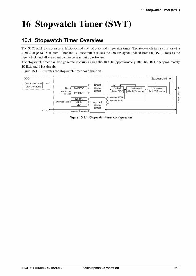
16 Stopwatch Timer (SWT)
S1C17611 TECHNICAL MANUAL Seiko Epson Corporation 16-1
16 Stopwatch Timer (SWT)
16.1 Stopwatch Timer OverviewThe S1C17611 incorporates a 1/100-second and 1/10-second stopwatch timer. The stopwatch timer consists of a 4-bit 2-stage BCD counter (1/100 and 1/10 second) that uses the 256 Hz signal divided from the OSC1 clock as the input clock and allows count data to be read out by software.The stopwatch timer can also generate interrupts using the 100 Hz (approximately 100 Hz), 10 Hz (approximately 10 Hz), and 1 Hz signals.Figure 16.1.1 illustrates the stopwatch timer configuration.
256Hz
Inte
rnal
dat
a b
us
Interrupt requestTo ITC
Feedbackdivision circuit
1/100-second4-bit BCD counter
1/10-second4-bit BCD counter
Countcontrolcircuit
Interrupt controlcircuit
SWTRUN
SIE100SIE10SIE1
Reset SWTRST
Stopwatch timerOSC
OSC1 oscillator/division circuit
Approximate 100 HzApproximate 10 Hz1Hz
RUN/STOPcontrol
Interrupt enable
Figure 16.1.1: Stopwatch timer configuration

16 Stopwatch Timer (SWT)
16-2 Seiko Epson Corporation S1C17611 TECHNICAL MANUAL
16.2 BCD CountersThe stopwatch timer consists of 1/100-second and 1/10-second 4-bit BCD counters.The count value can be read from the SWT_BCNT register.
1/100-second counter* BCD100[3:0]: 1/100 Sec. BCD Counter Value in the Stopwatch Timer BCD Counter (SWT_BCNT) Register
(D[3:0]/0x5021)
1/10-second counter* BCD10[3:0]: 1/10 Sec. BCD Counter Value in the Stopwatch Timer BCD Counter (SWT_BCNT) Register
(D[7:4]/0x5021)
Count-up Pattern A feedback division circuit is used to generate 100 Hz, 10 Hz, and 1 Hz signals from the 256 Hz clock. The
counter count-up pattern varies as shown in Figure 16.2.1.
3256
2256
3256
2256
3256
2256
3256
2256
3256
2256
1/100-second counter count-up pattern 1
256Hz
Approximate 100 Hz(Feedback division circuit output)
1/100-second counter
Approximate 10 Hz(1/100-second counter output)
Approximate 10 Hz(1/100-second counter output)
1/10-second counter
1Hz(1/10-second counter output)
25256
1/100-second counter count-up pattern 2
seconds
26256
× 6 + 25256
× 4 = 1 second
26256
seconds 26256
seconds 25256
seconds 25256
seconds 26256
seconds 26256
seconds 25256
seconds 25256
seconds 26256
seconds 26256
seconds
seconds26256
3256
3256
3256
2256
3256
2256
3256
2256
3256
2256
0 1 2 3 4 5 6 7 8 9
0 1 2 3 4 5 6 7 8 9
0 1 2 3 4 5 6 7 8 9
1/10-second counter count-up pattern
Figure 16.2.1: Stopwatch timer count-up patterns
The feedback division circuit generates an approximate 100 Hz signal at 2/256-second and 3/256-second intervals from the 256 Hz signal fed from the OSC module.
The 1/100-second counter counts the approximate 100 Hz signal output by the feedback division circuit and generates an approximate 10 Hz signal at 25/256-second and 26/256-second intervals.
Count-up will be pseudo 1/100-second counting at 2/256-second and 3/256-second intervals.
The 1/10-second counter counts the approximate 10 Hz signal generated by the 1/100-second counter at a ratio of 4:6, and generates a 1 Hz signal.
Count-up will be pseudo 1/10-second counting at 25/256-second and 26/256-second intervals.

16 Stopwatch Timer (SWT)
S1C17611 TECHNICAL MANUAL Seiko Epson Corporation 16-3
16.3 Operation ClockThe stopwatch timer uses the 256 Hz clock output by the OSC module as the operation clock.The OSC module generates this operation clock by dividing the OSC1 clock into 1/128, resulting in a frequency of 256 Hz when the OSC1 clock frequency is 32.768 kHz. The frequency described in this section will vary accordingly for other OSC1 clock frequencies.The OSC module does not include a 256 Hz clock output control bit. The 256 Hz clock is normally fed to the stopwatch timer when the OSC1 oscillation is on.For detailed information on OSC1 oscillator circuit control, refer to “7 Oscillator Circuit (OSC).”

16 Stopwatch Timer (SWT)
16-4 Seiko Epson Corporation S1C17611 TECHNICAL MANUAL
16.4 Stopwatch Timer ResettingReset the stopwatch timer by writing 1 to the SWTRST bit (D4/SWT_CTL register). This clears the counter to 0.
* SWTRST: Stopwatch Timer Reset Bit in the Stopwatch Timer Control (SWT_CTL) Register (D4/0x5020)
Apart from this operation, the counter is also cleared by initial resetting.

16 Stopwatch Timer (SWT)
S1C17611 TECHNICAL MANUAL Seiko Epson Corporation 16-5
16.5 Stopwatch Timer RUN/STOP ControlSet the following items before starting the stopwatch timer.(1) If using interrupts, set the interrupt level and permit interrupts for the stopwatch timer. See Section 16.6.(2) Reset the timer. See Section 16.4.
The stopwatch timer includes SWTRUN (D0/SWT_CTL register) to control Run/Stop.
* SWTRUN: Stopwatch Timer Run/Stop Control Bit in the Stopwatch Timer Control (SWT_CTL) Register (D0/0x5020)
The stopwatch timer starts counting when SWTRUN is written as 1. Writing 0 to SWTRUN prevents clock input and stops the count.This control does not affect the counter (SWT_BCNT register) data. The counter data is retained even when the count is halted, allowing resumption of the count from that data.If SWTRUN and SWTRST are written as 1 simultaneously, the stopwatch timer starts counting after the reset.
Interrupt factors are generated during counting at the corresponding 100 Hz (approximate 100 Hz), 10 Hz (approximate 10 Hz), and 1 Hz signal falling edges. If interrupts are permitted, interrupt requests are sent to the interrupt controller (ITC).
BCD100[0]
BCD100[1]
BCD100[2]
BCD100[3]
100 Hz interrupt
10 Hz interrupt
1/100-secondcounterBCD data
1/10-secondcounterBCD data
BCD10[0]
BCD10[1]
BCD10[2]
BCD10[3]
1 Hz interrupt
1 2 3 4 5 6 7 8 9 0 1 2 3 4 5 6 7 8 9 0 1 2 3 40
Figure 16.5.1: Stopwatch timer timing chart
Note: The stopwatch timer switches to Run/Stop mode when data is written to SWTRUN synchronized with the 256 Hz signal falling edge. When 0 is written to SWTRUN, the timer switches to Stop state after counting an additional “+1.” 1 is retained for SWTRUN reading until the timer actually stops.
Figure 16.5.2 shows the Run/Stop control timing chart.
SWTRUN(WR)
SWT_BCNT register 27 28 29 30 31 32
SWTRUN(RD)
256Hz
Figure 16.5.2: Run/Stop control timing chart

16 Stopwatch Timer (SWT)
16-6 Seiko Epson Corporation S1C17611 TECHNICAL MANUAL
16.6 Stopwatch Timer InterruptsThe SWT module includes functions for generating the following three kinds of interrupts:• 100 Hz interrupt• 10 Hz interrupt• 1 Hz interrupt
The SWT module outputs a single interrupt signal shared by the above three interrupt factors to the interrupt controller (ITC). The interrupt flag within the SWT module should be read to identify the interrupt factor that occurred.
100 Hz, 10 Hz, 1 Hz interrupts Generated at the 100 Hz (approximate 100 Hz), 10 Hz (approximate 10 Hz), and 1 Hz signal falling edges,
these interrupt requests set the following interrupt flags in the SWT module to 1.
* SIF1: 1 Hz Interrupt Flag in the Stopwatch Timer Interrupt Flag (SWT_IFLG) Register (D2/0x5023)* SIF10: 10 Hz Interrupt Flag in the Stopwatch Timer Interrupt Flag (SWT_IFLG) Register (D1/0x5023)* SIF100: 100 Hz Interrupt Flag in the Stopwatch Timer Interrupt Flag (SWT_IFLG) Register (D0/0x5023)
To use these interrupts, set the following interrupt enable bits to 1 for the corresponding interrupt flags. If the interrupt enable bits are set to 0 (default), the interrupt flag will not be set to 1, and the interrupt requests for this factor will not be sent to the ITC.
* SIE1: 1 Hz Interrupt Enable Bit in the Stopwatch Timer Interrupt Mask (SWT_IMSK) Register (D2/0x5022)* SIE10: 10 Hz Interrupt Enable Bit in the Stopwatch Timer Interrupt Mask (SWT_IMSK) Register (D1/0x5022)* SIE100: 100 Hz Interrupt Enable Bit in the Stopwatch Timer Interrupt Mask (SWT_IMSK) Register (D0/0x5022)
The SWT module outputs an interrupt request to the ITC if the SIF* is set to 1. This interrupt request signal generates an interrupt if the ITC and S1C17 core interrupt conditions are met.
Check the frequency of a stopwatch timer interrupt by reading SIF* as part of the stopwatch timer interrupt processing routine.
Note: • To prevent interrupt recurrences, the SWT module interrupt flag SIF*must be reset within the interrupt processing routine following a stopwatch timer interrupt.
• To prevent generating unnecessary interrupts, reset the corresponding SIF* before permitting stopwatch timer interrupt from SIE*.
Interrupt vectors The stopwatch timer interrupt vector numbers and vector addresses are listed below.
Vector number: 6 (0x06) Vector address: TTBR + 0x18
Other interrupt settings The ITC allows the priority of stopwatch timer interrupts to be set between level 0 (the default value) and level
7. To generate actual interrupts, the PSR (S1C17 core internal processor status register) IE (interrupt enable) bit must be set to 1.
For more information on interrupt processing, see “6 Interrupt Controller (ITC).”

16 Stopwatch Timer (SWT)
S1C17611 TECHNICAL MANUAL Seiko Epson Corporation 16-7
16.7 Control Register DetailsTable 16.7.1 Stopwatch timer register list
Address Register name Function0x5020 SWT_CTL Stopwatch Timer Control Register Timer resetting and Run/Stop control0x5021 SWT_BCNT Stopwatch Timer BCD Counter Register BCD counter data0x5022 SWT_IMSK Stopwatch Timer Interrupt Mask Register Interrupt mask setting
0x5023 SWT_IFLG Stopwatch Timer Interrupt Flag Register Interrupt occurrence status display/resetting
The stopwatch timer registers are described in detail below. These are 8-bit registers.
Note: When data is written to the registers, the “Reserved” bits must always be written as 0 and not 1.
16 Stopwatch Timer (SWT)
16-8 Seiko Epson Corporation S1C17611 TECHNICAL MANUAL
0x5020: Stopwatch Timer Control Register (SWT_CTL)Register name Address Bit Name Function Setting Init. R/W Remarks
Stopwatch Timer Control Register(SWT_CTL)
0x5020(8 bits)
D7–5 – reserved – – – 0 when being read.D4 SWTRST Stopwatch timer reset 1 Reset 0 Ignored 0 W
D3–1 – reserved – – –D0 SWTRUN Stopwatch timer run/stop control 1 Run 0 Stop 0 R/W
D[7:5] Reserved
D4 SWTRST: Stopwatch Timer Reset Bit Resets the stopwatch timer. 1 (W): Reset 0 (W): Disabled 0 (R): Normally 0 when read out (default)
Writing 1 to this bit resets the counter to 0x0. When reset in Run state, the stopwatch timer restarts immediately after resetting. The reset data 0x0 is retained when in Stop state.
D[3:1] Reserved
D0 SWTRUN: Stopwatch Timer Run/Stop Control Bit Controls the stopwatch timer Run/Stop. 1 (R/W): Run 0 (R/W): Stop (default)
The stopwatch timer starts counting when SWTRUN is written as 1 and stops when written as 0. The counter data is retained at Stop state until a reset or the next Run state.

16 Stopwatch Timer (SWT)
S1C17611 TECHNICAL MANUAL Seiko Epson Corporation 16-9
0x5021: Stopwatch Timer BCD Counter Register (SWT_BCNT)Register name Address Bit Name Function Setting Init. R/W Remarks
Stopwatch Timer BCD Counter Register(SWT_BCNT)
0x5021(8 bits)
D7–4
BCD10[3:0] 1/10 sec. BCD counter value 0 to 9 0 R
D3–0
BCD100[3:0] 1/100 sec. BCD counter value 0 to 9 0 R
D[7:4] BCD10[3:0]: 1/10 Sec. BCD Counter Value Read the 1/10-second counter BCD data. (Default: 0) This register is read-only and cannot be written to.
D[3:0] BCD100[3:0]: 1/100 Sec. BCD Counter Value Read the 1/100-second counter BCD data. (Default: 0) This register is read-only and cannot be written to.
Note: The correct counter value may not be read out (reading is unstable) if the register is read while counting is underway.
Obtain the counter value by one of the following methods: • Read the counter value while the counter is halted. • Read the counter twice in succession. Treat the value as valid if the values read are
identical.

16 Stopwatch Timer (SWT)
16-10 Seiko Epson Corporation S1C17611 TECHNICAL MANUAL
0x5022: Stopwatch Timer Interrupt Mask Register (SWT_IMSK)Register name Address Bit Name Function Setting Init. R/W Remarks
Stopwatch Timer Interrupt Mask Register(SWT_IMSK)
0x5022(8 bits)
D7–3 – reserved – – – 0 when being read.D2 SIE1 1 Hz interrupt enable 1 Enable 0 Disable 0 R/WD1 SIE10 10 Hz interrupt enable 1 Enable 0 Disable 0 R/WD0 SIE100 100 Hz interrupt enable 1 Enable 0 Disable 0 R/W
This register permits or prohibits interrupt requests individually for the stopwatch timer 100 Hz, 10 Hz, and 1 Hz signals. Setting the SIE*bit to 1 permits stopwatch timer interrupts for the corresponding frequency signal falling edge, while setting to 0 prohibits interrupts.
D[7:3] Reserved
D2 SIE1: 1 Hz Interrupt Enable Bit Permits or prohibits 1 Hz signal interrupts. 1 (R/W): Interrupt permitted 0 (R/W): Interrupt prohibited (default)
D1 SIE10: 10 Hz Interrupt Enable Bit Permits or prohibits 10 Hz signal interrupts. 1 (R/W): Interrupt permitted 0 (R/W): Interrupt prohibited (default)
D0 SIE100: 100 Hz Interrupt Enable Bit Permits or prohibits 100 Hz signal interrupts. 1 (R/W): Interrupt permitted 0 (R/W): Interrupt prohibited (default)

16 Stopwatch Timer (SWT)
S1C17611 TECHNICAL MANUAL Seiko Epson Corporation 16-11
0x5023: Stopwatch Timer Interrupt Flag Register (SWT_IFLG)Register name Address Bit Name Function Setting Init. R/W Remarks
Stopwatch Timer Interrupt Flag Register(SWT_IFLG)
0x5023(8 bits)
D7–3 – reserved – – – 0 when being read.D2 SIF1 1 Hz interrupt flag 1 Cause of
interrupt occurred
0 Cause of interrupt not occurred
0 R/W Reset by writing 1.D1 SIF10 10 Hz interrupt flag 0 R/WD0 SIF100 100 Hz interrupt flag 0 R/W
This register indicates the occurrence state of interrupt factors due to stopwatch timer 100 Hz, 10 Hz, and 1 Hz signals. If a stopwatch timer interrupt occurs, identify the interrupt factor (frequency) by reading the interrupt flag in this register. SIF* are SWT module interrupt flags corresponding to the individual 100 Hz, 10 Hz, and 1 Hz interrupts. It is set to 1 at the falling edge of each signal if SIE* (SWT_IMSK register) is set to 1. The stopwatch timer interrupt request signal is output to the ITC at the same time. This interrupt request signal generates an interrupt if the ITC and S1C17 core interrupt conditions are met.SIF* is reset by writing as 1.
Note: • To prevent interrupt recurrences, the SWT module interrupt flag SIF*must be reset within the interrupt processing routine following a stopwatch timer interrupt.
• To prevent generating unnecessary interrupts, SIF* must be reset before permitting stopwatch timer interrupts using SIE.*
D[7:3] Reserved
D2 SIF1: 1 Hz Interrupt Flag Interrupt flag indicating the 1 Hz interrupt factor occurrence status. 1(R): Interrupt factor present 0(R): No interrupt factor (default) 1(W): Reset flag 0(W): Disabled
Setting SIE1 (D2/SWT_IMSK register) to 1 sets SIF1 to 1 at the 1 Hz signal falling edge.
D1 SIF10: 10 Hz Interrupt Flag Interrupt flag indicating the 10 Hz interrupt factor occurrence status. 1(R): Interrupt factor present 0(R): No interrupt factor (default) 1(W): Reset flag 0(W): Disabled
Setting SIE10 (D1/SWT_IMSK register) to 1 sets SIF10 to 1 at the 10 Hz signal falling edge.
D0 SIF100: 100 Hz Interrupt Flag Interrupt flag indicating the 100 Hz interrupt factor occurrence status. 1(R): Interrupt factor present 0(R): No interrupt factor (default) 1(W): Reset flag 0(W): Disabled
Setting SIE100 (D0/SWT_IMSK register) to 1 sets SIF100 to 1 at the 100 Hz signal falling edge.

16 Stopwatch Timer (SWT)
16-12 Seiko Epson Corporation S1C17611 TECHNICAL MANUAL
16.8 Precautions• The OSC1 oscillator circuit must be set to On before operating the stopwatch timer.
• To prevent interrupt recurrences, the SWT_IFLG register interrupt flag must be reset within the interrupt processing routine following a stopwatch timer interrupt.
• To prevent generating unnecessary interrupts, reset the SWT_IFLG register interrupt flag before permitting stopwatch timer interrupts by the SWT_IMSK register.
• The stopwatch timer switches to Run/Stop mode when data is written to SWTRUN (D0/SWT_CTL resister) synchronized with the 256 Hz signal falling edge. When 0 is written to SWTRUN, the timer switches to Stop state after counting an additional “+1.” 1 is retained for SWTRUN reading until the timer actually stops.
Figure 16.8.1 shows the Run/Stop control timing chart.
SWTRUN(WR)
SWT_BCNT register 27 28 29 30 31 32
SWTRUN(RD)
256Hz
Figure 16.8.1: Run/Stop control timing chart
• Executing the slp instruction will destabilize a running stopwatch timer (SWTRUN = 1) during recovery from SLEEP state. When switching to SLEEP state, set the stopwatch timer to STOP (SWTRUN = 0) before executing the slp instruction.
• The correct counter value may not be read out (reading is unstable) if the counter register is read while counting is underway.
To obtain the counter value, read the counter register while the counter is halted or read the counter register twice in succession. Treat the value as valid if the values read are identical.

17 Watchdog Timer (WDT)
S1C17611 TECHNICAL MANUAL Seiko Epson Corporation 17-1
17 Watchdog Timer (WDT)
17.1 Watchdog Timer OverviewThe S1C17611 incorporates a watchdog timer that uses the OSC1 oscillator circuit as its oscillation source. The watchdog timer generates an NMI or reset (selectable via software) to the CPU if not reset within 131,072/fOSC1 seconds (4 seconds when fOSC1 = 32.768 kHz).Reset the watchdog timer via software within this cycle to prevent NMI/resets, which in turn enables runaway detection for programs that do not pass through the processing routine.Figure 17.1.1 illustrates the watchdog timer block diagram.
256Hz
NMIReset
10-bit counter
Interruptcontrol circuit
Run/Stop control
NMI/Reset mode selection
WDTRUN[3:0]
WDTMD
Watchdog timer reset WDTRST Watchdog timerOSC
OSC1 oscillation/division circuit
Figure 17.1.1: Watchdog timer block diagram

17 Watchdog Timer (WDT)
17-2 Seiko Epson Corporation S1C17611 TECHNICAL MANUAL
17.2 Operation ClockThe watchdog timer uses the 256 Hz clock output by the OSC module as the operation clock.The OSC module generates this operation clock by dividing the OSC1 clock into 1/128, resulting in a frequency of 256 Hz when the OSC1 clock frequency is 32.768 kHz. The frequency described in this section will vary accordingly for other OSC1 clock frequencies.The OSC module does not include a 256 Hz clock output control bit. The 256 Hz clock is normally fed to the watchdog timer when the OSC1 oscillation is on.For detailed information on OSC1 oscillator circuit control, refer to “7 Oscillator Circuit (OSC).”

17 Watchdog Timer (WDT)
S1C17611 TECHNICAL MANUAL Seiko Epson Corporation 17-3
17.3 Watchdog Timer Control
17.3.1 NMI/Reset Mode Selection
WDTMD (D1/WDT_ST register) is used to select whether an NMI signal or a reset signal is output when the watchdog timer has not been reset within the NMI/Reset occurrence cycle.
* WDTMD: NMI/Reset Mode Select Bit in the Watchdog Timer Status (WDT_ST) Register (D1/0x5041)
To generate an NMI, set WDTMD to 0 (default). Set to 1 to generate a reset.
17.3.2 Watchdog Timer Run/Stop Control
The watchdog timer starts counting when a value other than 0b1010 is written to WDTRUN[3:0] (D[3:0]/WDT_CTL register) and stops when 0b1010 is written.
* WDTRUN[3:0]: Watchdog Timer Run/Stop Control Bits in the Watchdog Timer Control (WDT_CTL) Register (D[3:0]/0x5040)
Initial resetting sets WDTRUN[3:0] to 0b1010 and stops the watchdog timer.Since an NMI or Reset may be generated immediately after running depending on the counter value, the watchdog timer should also be reset concurrently (before running the watchdog timer), as explained in the following section.
17.3.3 Watchdog Timer Resetting
To reset the watchdog timer, write 1 to WDTRST (D4/WDT_CTL register).
* WDTRST: Watchdog Timer Reset Bit in the Watchdog Timer Control (WDT_CTL) Register (D4/0x5040)
A location should be provided for periodically processing the routine for resetting the watchdog timer before an NMI or Reset is generated when using the watchdog timer. Process this routine within 131,072/fOSC1 second (4 seconds when fOSC1 = 32.768 kHz) cycle.After resetting, the watchdog timer starts counting with a new NMI/Reset generation cycle.
If the watchdog timer is not reset within the NMI/Reset generation cycle for any reason, the CPU is switched to interrupt processing by NMI or resetting, an interrupt vector is read out, and an interrupt processing routine is executed.The reset and NMI vector addresses are TTBR + 0x0 and TTBR + 0x08.
If the counter overflows and generates an NMI without the watchdog timer being reset, WDTST (D0/WDT_ST register) is set to 1.
* WDTST: NMI Status Bit in the Watchdog Timer Status (WDT_ST) Register (D0/0x5041)
This bit is provided to confirm that the watchdog timer was the source of the NMI.The WDTST set to 1 is cleared to 0 by resetting the watchdog timer.
17.3.4 Operation in Standby Mode
HALT mode The watchdog timer operates in HALT mode, as the clock is fed. HALT mode is therefore canceled by an NMI
or Reset if it continues for more than the NMI/Reset cycle. To disable the watchdog timer while in HALT mode, stop the watchdog timer by writing 0b1010 to WDTRUN[3:0] before executing the halt instruction. Reset the watchdog timer before resuming operations after HALT mode is canceled.
SLEEP mode The clock fed from the OSC module is stopped in SLEEP mode, which also stops the watchdog timer. To pre-
vent generation of an unnecessary NMI or Reset after canceling SLEEP mode, reset the watchdog timer before executing the slp instruction. The watchdog should also be stopped as required using WDTRUN[3:0].
17 Watchdog Timer (WDT)
17-4 Seiko Epson Corporation S1C17611 TECHNICAL MANUAL
17.4 Control Register DetailsTable 17.4.1 Watchdog timer register list
Address Register name Function0x5040 WDT_CTL Watchdog Timer Control Register Timer reset and Run/Stop control0x5041 WDT_ST Watchdog Timer Status Register Timer mode setting and NMI status display
The watchdog timer registers are described in detail below. These are 8-bit registers.
Note: When data is written to the registers, the “Reserved” bits must always be written as 0 and not 1.

17 Watchdog Timer (WDT)
S1C17611 TECHNICAL MANUAL Seiko Epson Corporation 17-5
0x5040: Watchdog Timer Control Register (WDT_CTL)Register name Address Bit Name Function Setting Init. R/W Remarks
Watchdog Timer Control Register(WDT_CTL)
0x5040(8 bits)
D7–5 – reserved – – – 0 when being read.D4 WDTRST Watchdog timer reset 1 Reset 0 Ignored 0 W
D3–0 WDTRUN[3:0] Watchdog timer run/stop control
Other than 1010Run
1010Stop
1010 R/W
D[7:5] Reserved
D4 WDTRST: Watchdog Timer Reset Bit Resets the watchdog timer. 1 (W): Reset 0 (W): Disabled 0 (R): Normally 0 when read out (default)
To use the watchdog timer, it must be reset by writing 1 to this bit within the NMI/Reset generation cycle (4 seconds when fOSC1 = 32.768 kHz).
This resets the up-counter to 0 and starts counting with a new NMI/Reset generation cycle.
D[3:0] WDTRUN[3:0]: Watchdog Timer Run/Stop Control Bits Controls the watchdog timer Run/Stop. Values other than 0b1010 (R/W): Run 0b1010 (R/W): Stop (default)
The watchdog timer must also be reset to prevent generation of an unnecessary NMI or Reset while the watchdog timer operates.

17 Watchdog Timer (WDT)
17-6 Seiko Epson Corporation S1C17611 TECHNICAL MANUAL
0x5041: Watchdog Timer Status Register (WDT_ST)Register name Address Bit Name Function Setting Init. R/W Remarks
Watchdog Timer Status Register(WDT_ST)
0x5041(8 bits)
D7–2 – reserved – – – 0 when being read.
D1 WDTMD NMI/Reset mode select 1 Reset 0 NMI 0 R/WD0 WDTST NMI status 1 NMI occurred 0 Not occurred 0 R
D[7:2] Reserved
D1 WDTMD: NMI/Reset Mode Select Bit Selects NMI or Reset generation on counter overflow. 1 (R/W): Reset 0 (R/W): NMI (default)
Setting this bit to 1 outputs a reset signal when the counter overflows. Setting to 0 outputs an NMI signal.
D0 WDTST: NMI Status Bit Indicates a counter overflow and NMI occurrence. 1 (R): NMI occurred (counter overflow) 0 (R): NMI did not occur (default)
This bit confirms that the watchdog timer was the source of the NMI. The WDTST set to 1 is cleared to 0 by resetting the watchdog timer.
This is also set by a counter overflow if reset output is selected, but is cleared by initial resetting and cannot be confirmed.
17 Watchdog Timer (WDT)
S1C17611 TECHNICAL MANUAL Seiko Epson Corporation 17-7
17.5 Precautions• When the watchdog timer is running, this must be reset by software within a 131,072/fOSC1 seconds (4 seconds
when fOSC1 = 32.768 kHz) cycle.
• The watchdog timer must also be reset to prevent generation of an unnecessary NMI or Reset while the watchdog timer operates.
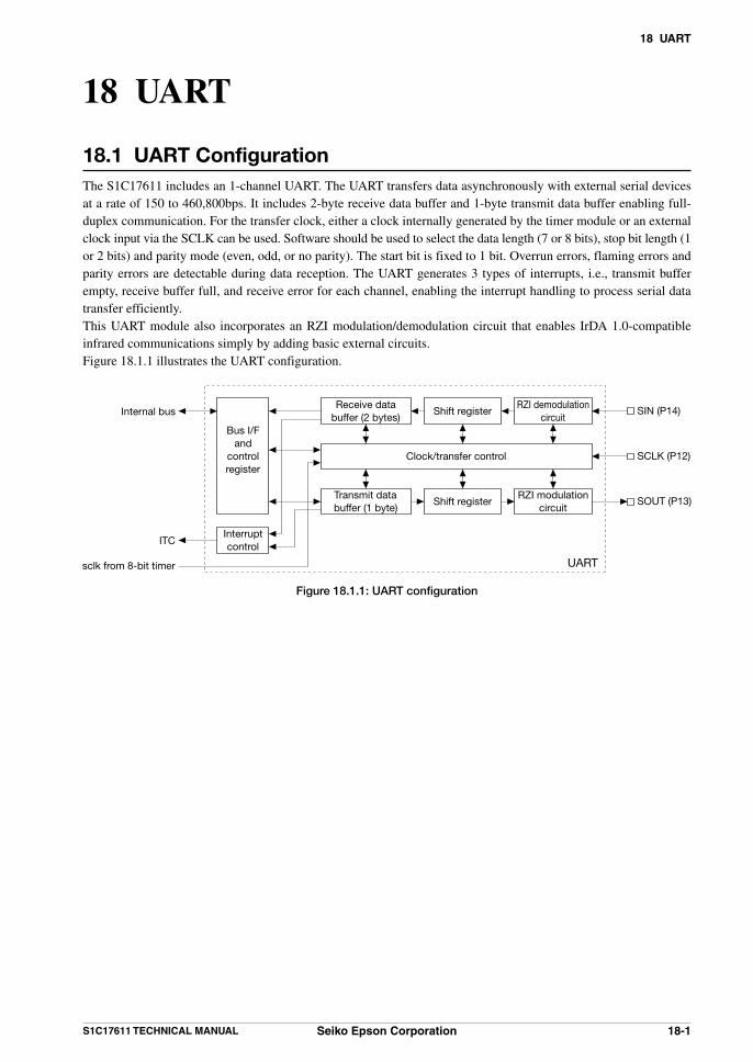
18 UART
S1C17611 TECHNICAL MANUAL Seiko Epson Corporation 18-1
18 UART
18.1 UART ConfigurationThe S1C17611 includes an 1-channel UART. The UART transfers data asynchronously with external serial devices at a rate of 150 to 460,800bps. It includes 2-byte receive data buffer and 1-byte transmit data buffer enabling full-duplex communication. For the transfer clock, either a clock internally generated by the timer module or an external clock input via the SCLK can be used. Software should be used to select the data length (7 or 8 bits), stop bit length (1 or 2 bits) and parity mode (even, odd, or no parity). The start bit is fixed to 1 bit. Overrun errors, flaming errors and parity errors are detectable during data reception. The UART generates 3 types of interrupts, i.e., transmit buffer empty, receive buffer full, and receive error for each channel, enabling the interrupt handling to process serial data transfer efficiently.This UART module also incorporates an RZI modulation/demodulation circuit that enables IrDA 1.0-compatible infrared communications simply by adding basic external circuits.Figure 18.1.1 illustrates the UART configuration.
Shift registerReceive data
buffer (2 bytes)SIN (P14)
sclk from 8-bit timer
Internal bus
ITC
UART
Bus I/F and
control register
SCLK (P12)
Shift registerTransmit databuffer (1 byte)
Clock/transfer control
SOUT (P13)
RZI demodulationcircuit
RZI modulation circuit
Interrupt control
Figure 18.1.1: UART configuration

18 UART
18-2 Seiko Epson Corporation S1C17611 TECHNICAL MANUAL
18.2 UART PinTable 18.2.1 lists the UART input/output pins.
Table 18.2.1: UART pin list
Pin name I/O Q’ty FunctionSIN (P14) I 1 UART data input pin
Inputs serial data sent from an external serial device.SOUT (P13) O 1 UART data output pin
Outputs serial data sent to an external serial device.SCLK (P12) I 1 UART clock input pin
Inputs the external clock when used for the transfer clock.
The UART input/output pins (SIN, SOUT, SCLK) are shared with general purpose input/output port pins (P14, P13, P12) and are initially set as general purpose input/output port pins. The function must be switched using the P1_PMUX register setting to use general purpose input/output port pins as UART input/output pins. Switch the pins to serial interface mode by setting the following control bits.
UART Ch.0P14 → SIN
* P14MUX: P14 Port Function Select Bit in the P1 Port Function Select (P1_PMUX) Register (D1-0/0x52a3)
P13 → SOUT* P13MUX: P13 Port Function Select Bit in the P1 Port Function Select (P1_PMUX) Register (D7-6/0x52a2)
P12 → SCLK (only when using external clock)* P12MUX: P12 Port Function Select Bit in the P1 Port Function Select (P1_PMUX) Register (D5-4/0x52a2)
For detailed information on pin function switching, refer to “10.2 Input/output Pin Function Selection (Port MUX).”

18 UART
S1C17611 TECHNICAL MANUAL Seiko Epson Corporation 18-3
18.3 Transfer ClockThe UART transfer clock can be set to internal or external using SSCK (D0/UART_MOD register).
* SSCK: Input Clock Select Bit in the UART Mode (UART_MOD) Register (D0/0x4103)
Note: Make sure the UART is halted (when RXEN/UART_CTL register = 0) before changing SSCK.
* RXEN: UART Enable Bit in the UART Control (UART_CTL) Register (D0/0x4104)
Internal clock Setting SSCK to 0 (the default value) selects the internal clock. UART uses the 8-bit timer output clock as the
transfer clock. Thus, bit timers must be programmed to output a clock suited to the transfer rate. For more information on 8-bit timer control, see “12 8-bit Timer (T8F).”
External clock Setting SSCK to 1 selects the external clock. In this case, set P12 to the SCLK pin (see Section 18.2) to input
the external clock.
Note: • The UART generates a sampling clock that divides the 8-bit timer output into 1/16 divisions. Be careful when setting the transfer rate.
• To input the external clock via the SCLK pin, the clock duty ratio must be 50%.

18 UART
18-4 Seiko Epson Corporation S1C17611 TECHNICAL MANUAL
18.4 Transfer Data SettingsSet the following conditions to set the transfer data format.• Data length: 7 or 8 bits• Start bit: Fixed at 1 bit• Stop bit: 1 or 2 bits• Parity bit: Even, odd, no parity
Note: Make sure the UART is halted (when RXEN/UART_CTL register = 0) before changing transfer data format settings.
* RXEN: UART Enable Bit in the UART Control (UART_CTL) Register (D0/0x4104)
Data length The data length is selected by CHLN (D4/UART_MOD register). Setting CHLN to 0 (default) sets the data
length to 7 bits. Setting CHLN to 1 sets the data length to 8 bits.
* CHLN: Character Length Select Bit in the UART Mode (UART_MOD) Register (D4/0x4103)
Stop bit The stop bit length is selected by STPB (D1/UART_MOD register). Setting STPB to 0 (default) sets the stop
bit length to 1 bit. Setting STPB to 1 sets the stop bit length to 2 bits.
* STPB: Stop Bit Select Bit in the UART Mode (UART_MOD) Register (D1/0x4103)
Parity bit Whether the parity function is enabled or disabled is selected by PREN (D3/UART_MOD register). Setting
PREN to 0 (default) disables the parity function. In this case, no parity bit is added to the transfer data and the data is not checked for parity when received. Setting PREN to 1 enables the parity function. In this case, a parity bit is added to the transfer data and the data is checked for parity when received.
When the parity function is enabled, the parity mode is selected by PMD (D2/UART_MOD register). Setting PMD to 0 (default) adds a parity bit and checks for even parity. Setting PMD to 1 adds a parity bit and checks for odd parity.
* PREN: Parity Enable Bit in the UART Mode (UART_MOD) Register (D3/0x4103)* PMD: Parity Mode Select Bit in the UART Mode (UART_MOD) Register (D2/0x4103)
Sampling clock (sclk•1/16)
CHLN = 0, PREN = 0, STPB = 0
CHLN = 0, PREN = 1, STPB = 0
CHLN = 0, PREN = 0, STPB = 1
CHLN = 0, PREN = 1, STPB = 1
CHLN = 1, PREN = 0, STPB = 0
CHLN = 1, PREN = 1, STPB = 0
CHLN = 1, PREN = 0, STPB = 1
CHLN = 1, PREN = 1, STPB = 1
s1: Start bit, s2 & s3: Stop bits, p: Parity bit
s1 D0 D1 D2 D3 D4 D5 D6 s2
s1 D0 D1 D2 D3 D4 D5 D6 p s2
s1 D0 D1 D2 D3 D4 D5 D6 s2 s3
s1 D0 D1 D2 D3 D4 D5 D6 p s2 s3
s1 D0 D1 D2 D3 D4 D5 D6 D7 s2
s1 D0 D1 D2 D3 D4 D5 D6 D7 p s2
s1 D0 D1 D2 D3 D4 D5 D6 D7 s2 s3
s1 D0 D1 D2 D3 D4 D5 D6 D7 p s2 s3
Figure 18.4.1: Transfer data format

18 UART
S1C17611 TECHNICAL MANUAL Seiko Epson Corporation 18-5
18.5 Data Transfer ControlMake the following settings before starting data transfers.(1) Select input clock. (See Section 18.3.) To use the internal clock, program the 8-bit timer to output the transfer clock. See Section 12.(2) Set the transfer data format. (See Section 18.4.)(3) To use the IrDA interface, set IrDA mode. (See Section 18.8.)(4) Set interrupt conditions to use UART interrupts. (See Section 18.7.)
Note: Make sure the UART is halted (when RXEN/UART_CTL register = 0) before changing the above settings.
* RXEN: UART Enable Bit in the UART Control (UART_CTL) Register (D0/0x4104)
Permitting data transfers Set the RXEN bit (D0/UART_CTL register) to 1 to permit data transfers. This switches transfer circuits to
enable transfers.
Note: Do not set the RXEN bit to 0 while the UART is sending or receiving data.
Data transfer control To start data transmission, program the transmission data to the UART_TXD register (0x4101).
* UART_TXD: UART Transmit Data Register (0x4101)
The data is written to the transmit data buffer, and the transmission circuit starts sending data. The buffer data is sent to the transmit shift register, and the start bit is output from the SOUT pin. The data in
the shift register is then output from the LSB. The transfer data bit is shifted in sync with the sampling clock rising edge and output in sequence via the SOUT pin. Following output of MSB, the parity bit (if parity is enabled) and stop bit are output.
The transmission circuit includes the TDBE (D0/UART_ST register) and TRBS (D2/UART_ST register) status flags.
* TDBE: Transmit Data Buffer Empty Flag in the UART Status (UART_ST) Register (D0/0x4100)* TRBS: Transmit Busy Flag in the UART Status (UART_ST) Register (D2/0x4100)
The TDBE flag indicates the transmit data buffer status. This flag switches to 0 when the application program programs data to the transmit data buffer and reverts to 1 when the buffer data is sent to the transmit shift register. Interrupts can be generated when this flag is 1 (see Section 18.7). Subsequent data is sent after confirming that the transmit data buffer is empty either by using this interrupt or by inspecting the TDBE flag. The transmission buffer size is 1 byte, but a shift register is provided separately to allow data to be written while the previous data is being sent. Always confirm that the transmit data buffer is empty before writing transmission data. Writing data while the TDBE flag is 0 will overprogram earlier transmission data inside the transmit data buffer.
The TRBS flag indicates the shift register status. This flag switches to 1 when transmission data is loaded from the transmit data buffer to the shift register and reverts to 0 once the data is sent. Read this flag to check whether the transmission circuit is operating or at standby.

18 UART
18-6 Seiko Epson Corporation S1C17611 TECHNICAL MANUAL
S1: Start bit, S2: Stop bit, P: Parity bit, Wr: data writing to transmit data buffer
Sampling clock
SOUT
TDBE
TRBS
Interrupt
S1 D0 D1 D2 D3 D4 D5 D6 D7 P S2 S1 D0 D1 D7 P S2 S1 D0 D1 D7 P
Wr Wr Wr
S2
Figure 18.5.1: Data transmission timing chart
Data reception control The receiving circuit is launched by setting the RXEN bit to 1, enabling data to be received from an external
serial device. When the external serial device sends the start bit, the receiving circuit detects its Low level and starts sampling
the following data bits. The data bits are sampled at the sampling clock rising edge, and the lead bit is loaded into the receive shift register as LSB. Once the MSB has been received into the shift register, the received data is loaded into the receive data buffer. If parity checking is enabled, the receiving circuit checks parity at the same time by checking the parity bit received immediately after the MSB.
The receive data buffer, a 2-byte FIFO, receives data until full.
Received data in the buffer can be read from the UART_RXD register (0x4102). The oldest data is read out first, clearing the register.
* UART_RXD: UART Receive Data Register (0x4102)
The receiving circuit includes the RDRY (D1/UART_ST register) and RD2B (D3/UART_ST register) buffer status flags.
* RDRY: Receive Data Ready Flag in the UART Status (UART_ST) Register (D1/0x4100)* RD2B: Second Byte Receive Flag in the UART Status (UART_ST) Register (D3/0x4100)
The RDRY flag indicates that the receive data buffer still contains data. The RD2B flag indicates that the receive data buffer is full.
(1) RDRY = 0, RD2B = 0 The receive data buffer contents need not be read, since no data has been received.
(2) RDRY = 1, RD2B = 0 One data has been received. Read the receive data buffer once. This reading resets the RDRY flag. The
buffer reverts to state (1) above. If the receive data buffer contents are read twice, the second data read will be invalid.
(3) RDRY = 1, RD2B = 1 Two data items have been received. Read the receive data buffer contents twice. The receive data buffer
outputs the oldest data first. This reading resets the RD2B flag. The buffer then reverts to the state in (2) above. The second read outputs the most recent received data, after which the buffer reverts to the state in (1) above.
Even when the receive data buffer is full, the shift register can start receiving one more 8-bit data. An overrun error will occur if receiving is finished before the receive data buffer has been read. In this case, the last received data cannot be read. The contents of the receive data buffer must be read out before an overrun error occurs. For detailed information on overrun errors, refer to Section 18.6.
The volume of data received can be checked by reading these flags.

18 UART
S1C17611 TECHNICAL MANUAL Seiko Epson Corporation 18-7
The UART allows receive buffer full interrupts to be generated once data has been received in the receive data buffer. These interrupts can be used to read the receive data buffer. With default settings, a receive buffer full interrupt occurs when the receive data buffer receives one item of data (status (2) above). This can be changed by setting the RBFI bit (D1/UART_CTL register) to 1 so that an interrupt occurs when the receive data buffer receives two items of data.
* RBFI: Receive Buffer Full Interrupt Condition Setup Bit in the UART Control (UART_CTL) Register (D1/0x4104)
Three error flags are also provided in addition to the flags previously mentioned. See Section 18.6 for detailed information on flags and receive errors.
Receive buffer full interrupt request(RBFI = 0)
Overrun errorinterrupt request
Sampling clock
SIN
Receive data buffer
RDRY
RD2B
RXD[7:0]
Interrupt
data 1S1 D0 ··· P S2 S1 D0 ··· P S2 S1 D0 ··· P S2 S1 D0 ··· P S2 S1 D0 ··· P S2 S1 D0 ··· P S2
data 2 data 3 data 4 data 5 data 6
Rd
Rd
data 3, 4data 2data 1 – data 2, 3 data 3
data 3data 2data 1
S1: Start bit, S2: Stop bit, P: Parity bit, Rd: Data read from RXD[7:0]
Figure 18.5.2: Data receiving timing chart
Blocking data transfers After a data transfer is completed (both transmission and reception), data transfers are blocked by writing 0 to
the RXEN bit. Confirm that the TDBE flag is 1 before blocking data transfer. Setting the RXEN bit to 0 empties the transmission data buffers (clearing any remaining data). The data being
transferred cannot be guaranteed if RXEN is set to 0 while data is being sent or received.

18 UART
18-8 Seiko Epson Corporation S1C17611 TECHNICAL MANUAL
18.6 Receive ErrorsThree different receive errors may be detected while receiving data.Since receive errors are interrupt factors, they can be processed by generating interrupts. For more information on UART interrupt control, refer to Section 18.7.
Parity error If PREN (D3/UART_MOD register) has been set to 1 (parity enabled), data received is checked for parity. Data received in the shift register is checked for parity when sent to the receive data buffer. The matching is
checked against the PMD (D2/UART_MOD register) setting (odd or even parity). If the result is a non-match, a parity error is issued, and the parity error flag PER (D5/UART_ST register) is set to 1.
Even if this error occurs, the data received is sent to the receive data buffer, and the receiving operation continues. However, the received data cannot be guaranteed if a parity error occurs.
The PER flag (D5/UART_ST register) is reset to 0 by writing as 1.
* PREN: Parity Enable Bit in the UART Mode (UART_MOD) Register (D3/0x4103)* PMD: Parity Mode Select Bit in the UART Mode (UART_MOD) Register (D2/0x4103)* PER: Parity Error Flag in the UART Status (UART_ST) Register (D5/0x4100)
Framing error A framing error occurs if the stop bit is received as 0 and the UART determines sync offset. If the stop bit is set
to two bits, only the first bit is checked. The framing error flag FER (D6/UART_ST register) is set to 1 if this error occurs. The received data is still
transferred to the receive data buffer if this error occurs and the receiving operation continues, but the data cannot be guaranteed, even if no framing error occurs for subsequent data receiving.
The FER flag (D6/UART_ST register) is reset to 0 by writing as 1.
* FER: Framing Error Flag in the UART Status (UART_ST) Register (D6/0x4100)
Overrun error Even if the receive data buffer is full (two data items already received), a third item of data can be received in
the shift register. However, if the receive data buffer is not emptied (by reading out data received) by the time this data has been received, the third data received in the shift register will not be sent to the buffer and generate an overrun error.
If an overrun error occurs, the overrun error flag OER (D4/UART_ST register) is set to 1. The receiving operation continues even if this error occurs. The OER flag (D4/UART_ST register) is reset to 0 by writing as 1.
* OER: Overrun Error Flag in the UART Status (UART_ST) Register (D4/0x4100)

18 UART
S1C17611 TECHNICAL MANUAL Seiko Epson Corporation 18-9
18.7 UART InterruptsThe UART includes a function for generating the following three different interrupt types.• Transmit buffer empty interrupt• Receive buffer full interrupt• Receive error interrupt
The UART outputs one interrupt signal shared by the three above interrupt factor types to the interrupt controller (ITC). (Two channels output two interrupt signals in total.) Inspect the status flag or error flag to determine the interrupt factor occurring.
Transmit buffer empty interrupt To use this interrupt, set TIEN (D4/UART_CTL register) to 1. If TIEN is set to 0 (default), interrupt requests
for this factor will not be sent to the ITC.
* TIEN: Transmit Buffer Empty Interrupt Enable Bit in the UART Control (UART_CTL) Register (D4/0x4104)
When transmission data written to the transmit data buffer is transferred to the shift register, the UART sets the TDBE bit (D0/UART_ST register) to 1, indicating that the transmit data buffer is empty. If transmit buffer empty interrupts are permitted (TIEN = 1), an interrupt request pulse is sent simultaneously to the ITC.
* TDBE: Transmit Data Buffer Empty Flag in the UART Status (UART_ST) Register (D0/0x4100)
An interrupt occurs if other interrupt conditions are met. You can inspect the TDBE flag in the UART interrupt handler routine to determine whether the UART interrupt
is attributable to a transmit buffer empty. If TDBE is 1, the next transmission data can be written to the transmit data buffer by the interrupt handler routine.
Receive buffer full interrupt To use this interrupt, set RIEN (D5/UART_CTL register) to 1. If RIEN is set to 0 (default), interrupt requests
for this factor will not be sent to the ITC.
* RIEN: Receive Buffer Full Interrupt Enable Bit in the UART Control (UART_CTL) Register (D5/0x4104)
If the specified volume of received data is loaded into the receive data buffer when a receive buffer full interrupt is permitted (RIEN = 1), the UART outputs an interrupt request pulse to the ITC. If RBFI (D1/UART_CTL register) is 0, an interrupt request pulse is output as soon as one item of received data is loaded into the receive data buffer (RDRY flag (D1/UART_ST register) is set to 1). If RBFI (D1/UART_CTL register) is 1, an interrupt request pulse is output as soon as two items of received data are loaded into the receive data buffer (RD2B flag (D3/UART_ST register) is set to 1).
* RBFI: Receive Buffer Full Interrupt Condition Setup Bit in the UART Control (UART_CTL) Register (D1/0x4104)* RDRY: Receive Data Ready Flag in the UART Status (UART_ST) Register (D1/0x4100)* RD2B: Second Byte Receive Flag in the UART Status (UART_ST) Register (D3/0x4100)
An interrupt occurs if other interrupt conditions are met. You can inspect the RDRY and RD2B flags in the UART interrupt handler routine to determine whether the
UART interrupt is attributable to a receive buffer full. If RDRY or RD2B is 1, the received data can be read from the receive data buffer by the interrupt handler routine.

18 UART
18-10 Seiko Epson Corporation S1C17611 TECHNICAL MANUAL
Receive error interrupt To use this interrupt, set REIEN (D6/UART_CTL register) to 1. If REIEN is set to 0 (default), interrupt requests
will not be sent to the ITC for this factor.
* REIEN: Receive Error Interrupt Enable Bit in the UART Control (UART_CTL) Register (D6/0x4104)
The UART sets the error flags shown below to 1 if a parity error, framing error, or overrun error is detected when receiving data. If receive error interrupts are permitted (REIEN = 1), an interrupt request pulse is output at the same time to the ITC.
* PER: Parity Error Flag in the UART Status (UART_ST) Register (D5/0x4100)* FER: Framing Error Flag in the UART Status (UART_ST) Register (D6/0x4100)* OER: Overrun Error Flag in the UART Status (UART_ST) Register (D4/0x4100)
If other interrupt conditions are satisfied, an interrupt occurs. Inspect the error flags above as part of the UART interrupt handler routine to determine whether the UART
interrupt was caused by a receive error. If any of the error flags has the value 1, the interrupt handler routine will proceed with error recovery.
Interrupt vectors The UART interrupt vector numbers and vector addresses are as listed below.
Table 18.7.1: UART interrupt vector
Vector number Vector address16(0x10) TTBR + 0x40
Other interrupt settings The ITC allows the priority of UART interrupts to be set between level 0 (the default value) and level 7 for
each channel. To generate actual interrupts, the PSR (S1C17 core internal processor status register) IE (interrupt enable) bit must be set to 1.
For more information on interrupt processing, see “6 Interrupt Controller (ITC).”

18 UART
S1C17611 TECHNICAL MANUAL Seiko Epson Corporation 18-11
18.8 IrDA InterfaceThis UART module incorporates an RZI modulation/demodulation circuit enabling implementation of IrDA 1.0-compatible infrared communication simply by adding basic external circuits.
The transmission data output from the UART transmit shift register is input to the modulation circuit and output from the SOUT pin after the Low pulse has been modulated to a 3 sclk cycle.
sclk
Modulation circuit input (shift register output)
Modulation circuit output (SOUT)
1 2 3 8 9 10 11 16
3 × sclk
Modulation circuit input (shift register output)
Modulation circuit output (SOUT)
S1 D0 D1 D2 D3 D4 D5 D6 D7 P S2 S3
(S1: Start bit, S2 & S3: Stop bits, P: Parity bit)
Figure 18.8.1: Transmission signal waveform
The received IrDA signal is input to the demodulation circuit and the Low pulse width is converted to 16 sclk cycles before entry to the receive shift register. The demodulation circuit uses the pulse detection clock selected from the prescaler output clock separately from the transfer clock to detect Low pulses input (when minimum pulse width = 1.41 μs/115,200 bps).
(S1: Start bit, S2 & S3: Stop bits, P: Parity bit)
sclk
irclk
Demodulation circuit input (SIN)
Demodulation circuit output (shift register input)
1 2 3 4 16
16 × sclkAt least 2 × irclk
Demodulation circuit input (SIN)
S1 D0 D1 D2 D3 D4 D5 D6 D7 P S2 S3Demodulation circuit output (shift register input)
Figure 18.8.2: Receive signal waveform
IrDA enable To use the IrDA interface function, set IRMD (D0/UART_EXP register) to 1. This enables the RZI modulation/
demodulation circuit.
* IRMD: IrDA Mode Select Bit in the UART Expansion (UART_EXP) Register (D0/0x4105)
Note: This must be set before setting other UART conditions.
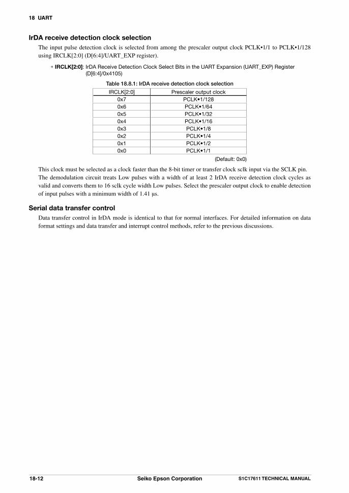
18 UART
18-12 Seiko Epson Corporation S1C17611 TECHNICAL MANUAL
IrDA receive detection clock selection The input pulse detection clock is selected from among the prescaler output clock PCLK•1/1 to PCLK•1/128
using IRCLK[2:0] (D[6:4]/UART_EXP register).
* IRCLK[2:0]: IrDA Receive Detection Clock Select Bits in the UART Expansion (UART_EXP) Register (D[6:4]/0x4105)
Table 18.8.1: IrDA receive detection clock selection
IRCLK[2:0] Prescaler output clock0x7 PCLK•1/1280x6 PCLK•1/640x5 PCLK•1/320x4 PCLK•1/160x3 PCLK•1/80x2 PCLK•1/40x1 PCLK•1/20x0 PCLK•1/1
(Default: 0x0)
This clock must be selected as a clock faster than the 8-bit timer or transfer clock sclk input via the SCLK pin. The demodulation circuit treats Low pulses with a width of at least 2 IrDA receive detection clock cycles as
valid and converts them to 16 sclk cycle width Low pulses. Select the prescaler output clock to enable detection of input pulses with a minimum width of 1.41 μs.
Serial data transfer control Data transfer control in IrDA mode is identical to that for normal interfaces. For detailed information on data
format settings and data transfer and interrupt control methods, refer to the previous discussions.

18 UART
S1C17611 TECHNICAL MANUAL Seiko Epson Corporation 18-13
18.9 Control Register DetailsTable 18.9.1: UART register list
Address Register name Function0x4100 UART_ST UART Status Register Transfer, buffer, error status display0x4101 UART_TXD UART Transmit Data Register Transmission data0x4102 UART_RXD UART Receive Data Register Received data
0x4103 UART_MOD UART Mode Register Transfer data format setting0x4104 UART_CTL UART Control Register Data transfer control0x4105 UART_EXP UART Expansion Register IrDA mode setting
The UART registers are described in detail below. These are 8-bit registers.
Note: When data is written to the registers, the “Reserved” bits must always be written as 0 and not 1.

18 UART
18-14 Seiko Epson Corporation S1C17611 TECHNICAL MANUAL
0x4100: UART Status Register (UART_ST)Register name Address Bit Name Function Setting Init. R/W Remarks
UART Status Register(UART_ST)
0x4100(8 bits)
D7 – reserved – – – 0 when being read.D6 FER Framing error flag 1 Error 0 Normal 0 R/W Reset by writing 1.D5 PER Parity error flag 1 Error 0 Normal 0 R/WD4 OER Overrun error flag 1 Error 0 Normal 0 R/WD3 RD2B Second byte receive flag 1 Ready 0 Empty 0 RD2 TRBS Transmit busy flag 1 Busy 0 Idle 0 R Shift register statusD1 RDRY Receive data ready flag 1 Ready 0 Empty 0 RD0 TDBE Transmit data buffer empty flag 1 Empty 0 Not empty 1 R
D7 Reserved
D6 FER: Framing Error Flag Indicates whether a framing error has occurred. 1 (R): Error occurred 0 (R): No error (default) 1 (W): Reset to 0 0 (W): Disabled
FER is set to 1 when a framing error occurs. Framing errors occur when data is received with the stop bit set to 0.
FER is reset by writing 1.
D5 PER: Parity Error Flag Indicates whether a parity error has occurred. 1 (R): Error occurred 0 (R): No error (default) 1 (W): Reset to 0 0 (W): Disabled
PER is set to 1 when a parity error occurs. Parity checking is enabled only when PREN (D3/UART_MOD register) is set to 1 and is performed when received data is transferred from the shift register to the receive data buffer.
PER is reset by writing 1.
D4 OER: Overrun Error Flag Indicates whether an overrun error has occurred. 1 (R): Error occurred 0 (R): No error (default) 1 (W): Reset to 0 0 (W): Disabled
OER is set to 1 when an overrun error occurs. Overrun errors occur when data is received in the shift register when the receive data buffer is already full and additional data is sent. The receive data buffer is not overwritten if this error occurs. The shift register is overwritten as soon as the error occurs.
OER is reset by writing 1.
D3 RD2B: Second Byte Received Flag Indicates that the receive data buffer contains two items of received data. 1 (R): Second byte can be read 0 (R): Second byte not received (default)
RD2B is set to 1 when the second byte of data is loaded into the receive data buffer and is reset to 0 when the first data is read from the receive data buffer.

18 UART
S1C17611 TECHNICAL MANUAL Seiko Epson Corporation 18-15
D2 TRBS: Transmit Busy Flag Indicates the transmit shift register status. 1 (R): Operating 0 (R): Standby (default)
TRBS is set to 1 when transmission data is loaded from the transmit data buffer into the shift register and is reset to 0 when the data transfer is complete. Inspect TRBS to determine whether the transmit circuit is operating or at standby.
D1 RDRY: Receive Data Ready Flag Indicates that the receive data buffer contains valid received data. 1 (R): Data can be read 0 (R): Buffer empty (default)
RDRY is set to 1 when received data is loaded into the receive data buffer and is reset to 0 when all data has been read from the receive data buffer.
D0 TDBE: Transmit Data Buffer Empty Flag Indicates the state of the transmit data buffer. 1 (R): Buffer empty (default) 0 (R): Data exists
TDBE is reset to 0 when transmit data is written to the transmit data buffer and is set to 1 when the data is transferred to the shift register.

18 UART
18-16 Seiko Epson Corporation S1C17611 TECHNICAL MANUAL
0x4101: UART Transmit Data Register (UART_TXD)Register name Address Bit Name Function Setting Init. R/W Remarks
UART Transmit Data Register(UART_TXD)
0x4101(8 bits)
D7–0 TXD[7:0] Transmit dataTXD7(6) = MSBTXD0 = LSB
0x0 to 0xff (0x7f) 0x0 R/W
D[7:0] TXD[7:0]: Transmit Data Program transmit data to be set in the transmit data buffer. (Default: 0x0) The UART begins transmitting when data is written to this register. Data written to TXD[7:0] is
retained until sent to the transmit data buffer. Transmitting data from within the transmit data buffer generates a transmit buffer empty interrupt
factor. TXD7 (MSB) is invalid in 7-bit mode. Serial converted data is output from the SOUT pin, with the LSB first bits set to 1 as High level and bits
set to 0 as Low level. This register can also be read from.

18 UART
S1C17611 TECHNICAL MANUAL Seiko Epson Corporation 18-17
0x4102: UART Receive Data Register (UART_RXD)Register name Address Bit Name Function Setting Init. R/W Remarks
UART ReceiveData Register(UART_RXD)
0x4102(8 bits)
D7–0 RXD[7:0] Receive data in the receive data bufferRXD7(6) = MSBRXD0 = LSB
0x0 to 0xff (0x7f) 0x0 R Older data in the buffer is read out first.
D[7:0] RXD[7:0]: Receive Data Data in the receive data buffer is read out in sequence, starting with the oldest. Received data is placed
in the receive data buffer. The receive data buffer is a 2-byte FIFO that allows proper data receipt until it fills, even if data is not read out. If the buffer is full and the shift register also contains received data, an overrun error will occur, unless the data is read out before receipt of the subsequent data starts.
The receive circuit includes two receive buffer status flags: RDRY (D1/UART_ST register) and RD2B (D3/UART_ST register). The RDRY flag indicates the presence of valid received data in the receive data buffer, while RD2B flag indicates the presence of two items of received data in the receive data buffer.
A receive buffer full interrupt occurs when the received data in the receive data buffer reaches the number specified by RBFI (D1/UART_CTL register).
0 is loaded into RXD7 in 7-bit mode. Serial data input via the SIN pin is converted to parallel, with the initial bit as LSB, the High level bit as 1,
and the Low level bit as 0. This data is then loaded into the receive data buffer. This register is read-only. (Default: 0x0)
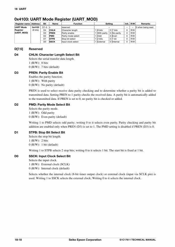
18 UART
18-18 Seiko Epson Corporation S1C17611 TECHNICAL MANUAL
0x4103: UART Mode Register (UART_MOD)Register name Address Bit Name Function Setting Init. R/W Remarks
UART Mode Register(UART_MOD)
0x4103(8 bits)
D7–5 – reserved – – – 0 when being read.D4 CHLN Character length 1 8 bits 0 7 bits 0 R/WD3 PREN Parity enable 1 With parity 0 No parity 0 R/WD2 PMD Parity mode select 1 Odd 0 Even 0 R/WD1 STPB Stop bit select 1 2 bits 0 1 bit 0 R/WD0 SSCK Input clock select 1 External 0 Internal 0 R/W
D[7:5] Reserved
D4 CHLN: Character Length Select Bit Selects the serial transfer data length. 1 (R/W): 8 bits 0 (R/W): 7 bits (default)
D3 PREN: Parity Enable Bit Enables the parity function. 1 (R/W): With parity 0 (R/W): No parity (default)
PREN is used to select receive data parity checking and to determine whether a parity bit is added to transmitted data. Setting PREN to 1 parity-checks the received data. A parity bit is automatically added to the transmitted data. If PREN is set to 0, no parity bit is checked or added.
D2 PMD: Parity Mode Select Bit Selects the parity mode. 1 (R/W): Odd parity 0 (R/W): Even parity (default)
Writing 1 to PMD selects odd parity; writing 0 to it selects even parity. Parity checking and parity bit addition are enabled only when PREN (D3) is set to 1. The PMD setting is disabled if PREN (D3) is 0.
D1 STPB: Stop Bit Select Bit Selects the stop bit length. 1 (R/W): 2 bits 0 (R/W): 1 bit (default)
Writing 1 to STPB selects 2 stop bits; writing 0 to it selects 1 bit. The start bit is fixed at 1 bit.
D0 SSCK: Input Clock Select Bit Selects the input clock. 1 (R/W): External clock (SCLK) 0 (R/W): Internal clock (default)
Selects whether the internal clock (8-bit timer output clock) or external clock (input via SCLK pin) is used. Writing 1 to SSCK selects the external clock; Writing 0 to it selects the internal clock.

18 UART
S1C17611 TECHNICAL MANUAL Seiko Epson Corporation 18-19
0x4104: UART Control Register (UART_CTL)Register name Address Bit Name Function Setting Init. R/W Remarks
UART Control Register(UART_CTL)
0x4104(8 bits)
D7 – reserved – – – 0 when being read.D6 REIEN Receive error int. enable 1 Enable 0 Disable 0 R/WD5 RIEN Receive buffer full int. enable 1 Enable 0 Disable 0 R/WD4 TIEN Transmit buffer empty int. enable 1 Enable 0 Disable 0 R/W
D3–2 – reserved – – – 0 when being read.D1 RBFI Receive buffer full int. condition 1 2 bytes 0 1 byte 0 R/WD0 RXEN UART enable 1 Enable 0 Disable 0 R/W
D7 Reserved
D6 REIEN: Receive Error Interrupt Enable Bit Permits interrupt requests to the ITC when a receive error occurs. 1 (R/W): Permitted 0 (R/W): Prohibited (default)
Set this bit to 1 to process receive errors using interrupts.
D5 RIEN: Receive Buffer Full Interrupt Enable Bit Permits interrupt requests to the ITC caused when the received data quantity in the receive data buffer
reaches the quantity specified in RBFI (D1). 1 (R/W): Permitted 0 (R/W): Prohibited (default)
Set this bit to 1 to read receive data using interrupts.
D4 TIEN: Transmit Buffer Empty Interrupt Enable Bit Permits interrupt requests to the ITC caused when transmission data in the transmit data buffer is sent
to the shift register (i.e. when data transmission begins). 1 (R/W): Permitted 0 (R/W): Prohibited (default)
Set this bit to 1 to program data to the transmit data buffer using interrupts.
D[3:2] Reserved
D1 RBFI: Receive Buffer Full Interrupt Condition Setup Bit Sets the quantity of data in the receive buffer to generate a receive buffer full interrupt. 1 (R/W): 2 bytes 0 (R/W): 1 byte (default)
If receive buffer full interrupts are permitted (RIEN = 1), the UART outputs an interrupt request pulse to the ITC when the quantity of received data specified by RBFI is loaded into the receive data buffer. If the RBFI bit is 0, an interrupt request pulse is output as soon as one item of received data is loaded into the receive data buffer (when the RDRY flag (D1/UART_ST register) is set to 1). If RBFI is 1, an interrupt request pulse is output as soon as two items of received data are loaded into the receive data buffer (when the RD2B flag (D3/UART_ST register) is set to 1).
D0 RXEN: UART Enable Bit Permits data transfer by the UART. 1 (R/W): Permitted 0 (R/W): Prohibited (default)
Set RXEN to 1 before starting UART transfers. Setting RXEN to 0 will stop data transfers. Set the transfer conditions while RXEN is 0.
Preventing transfers by writing 0 to RXEN also clears transmit data buffer.

18 UART
18-20 Seiko Epson Corporation S1C17611 TECHNICAL MANUAL
0x4105: UART Expansion Register (UART_EXP)Register name Address Bit Name Function Setting Init. R/W Remarks
UART Expansion Register(UART_EXP)
0x4105(8 bits)
D7 – reserved – – – 0 when being read.D6–4 IRCLK[2:0] IrDA receive detection clock
selectIRCLK[2:0] Clock 0x0 R/W
0x70x60x50x40x30x20x10x0
PCLK•1/128PCLK•1/64PCLK•1/32PCLK•1/16PCLK•1/8PCLK•1/4PCLK•1/2PCLK•1/1
D3–1 – reserved – – – 0 when being read.D0 IRMD IrDA mode select 1 On 0 Off 0 R/W
D7 Reserved
D[6:4] IRCLK[2:0]: IrDA Receive Detection Clock Select Bits Select the prescaler output clock used as the IrDA input pulse detection clock.
Table 18.9.2: IrDA receive detection clock selection
IRCLK[2:0] Prescaler output clock0x7 PCLK•1/1280x6 PCLK•1/640x5 PCLK•1/320x4 PCLK•1/160x3 PCLK•1/80x2 PCLK•1/40x1 PCLK•1/20x0 PCLK•1/1
(Default: 0x0)
This clock must be selected as a clock faster than the 8-bit timer or transfer clock sclk input via the SCLK pin.
The demodulation circuit treats Low pulses with a width of at least 2 IrDA receive detection clock cycles as valid. Select the appropriate prescaler output clock to enable detection of input pulses with a minimum width of 1.41 μs.
D[3:1] Reserved
D0 IRMD: IrDA Mode Select Bit Switches the IrDA interface function on and off. 1 (R/W): On 0 (R/W): Off (default)
Set this to 1 to use the IrDA interface. When this bit is set to 0, this module functions as a normal UART, with no IrDA functions.

18 UART
S1C17611 TECHNICAL MANUAL Seiko Epson Corporation 18-21
18.10 Precautions• The following UART bits should be set with transfers blocked (RXEN = 0).
- All UART_MOD register (0x4103) bits (SSCK, STPB, PMD, PREN, CHLN)- RBFI bit in the UART_CTLx register- All UART_EXP register (0x4105) bits (IRMD, IRCLK[2:0])
* RXEN: UART Enable Bit in the UART Control (UART_CTL) Register (D0/0x4104)
• Do not set RXEN to 0 while the UART is transmitting or receiving data.
• The UART transfer rate is capped at 460,800 bps. Do not set faster transfer rates.
• Preventing transfer by setting RXEN to 0 clears (initializes) transfer data buffers. Before writing 0 to RXEN, confirm the absence of data in the buffers awaiting transmission.
• The IrDA receive detection clock must be selected as a clock faster than the 8-bit timer or transfer clock sclk input via the SCLK pin.
• The IrDA interface demodulation circuit treats Low pulses with a width of at least 2 IrDA receive detection clock cycles as valid. Select the appropriate prescaler output clock to enable detection of input pulses with a minimum width of 1.41 μs as an IrDA receive detection clock.

19 SPI
S1C17611 TECHNICAL MANUAL Seiko Epson Corporation 19-1
19 SPI
19.1 SPI ConfigurationThe S1C17611 incorporates a synchronized serial interface module (SPI). This SPI module supports both Master and Slave modes and is used for 8-bit data transfers. Four different data transfer timing patterns (clock phase and polarity) can be selected.The SPI module includes a transmit data buffer and receive data buffer separate from the shift register, and is capable of generating two different interrupt types (transmit buffer empty and receive buffer full). This allows easy processing of continuous serial data transfer using interrupts.The transmit buffer empty interrupt can be used by only Master mode.Figure 19.1.1 illustrates the SPI module configuration.
SDI
PCLK
ITC
SPI
SPICLK#SPISS
SDO
1/4
Shift registerReceive databuffer (1 byte)
16-bit timer Ch.1output clock
Bus I/F and
control register
Shift registerTransmit databuffer (1 byte)
Clock/transfer control
Interrupt control
Internal bus
Figure 19.1.1: SPI module configuration

19 SPI
19-2 Seiko Epson Corporation S1C17611 TECHNICAL MANUAL
19.2 SPI Input/Output PinsTable 19.2.1 lists the SPI pins.
Table 19.2.1: SPI pin list
Pin name I/O Q’ty FunctionSDI (P16) I 1 SPI data input pin
Inputs serial data from SPI bus.SDO (P17) O 1 SPI data output pin
Outputs serial data to SPI bus.SPICLK (P20) I/O 1 SPI external clock input/output pin
Outputs SPI clock when SPI is in Master mode.Inputs external clock when SPI is used in Slave mode.
#SPISS (P15) I 1 SPI slave selection signal (active Low) input pinSPI (Slave mode) is selected as slave device by Low input to this pin.
The SPI input/output pins (SDI, SDO, SPICLK, #SPISS) are shared with general purpose input/output port pins (P16, P17, P20, P15) and are initially set as general purpose input/output port pins. The function must be switched using the P2_PMUX, P1_PMUX registers settings to use general purpose input/output port pins as SPI input/output pins. Switch the pins to SPI mode by setting the following control bits.
P16 → SDI* P16MUX: P16 Port Function Select Bit in the P1 Port Function Select (P1_PMUX) Register (D5-4/0x52a3)
P17 → SDO* P17MUX: P17 Port Function Select Bit in the P1 Port Function Select (P1_PMUX) Register (D7-6/0x52a3)
P20 → SPICLK* P20MUX: P20 Port Function Select Bit in the P2 Port Function Select (P2_PMUX) Register (D1-0/0x52a4)
P15 → #SPISS* P15MUX: P15 Port Function Select Bit in the P1 Port Function Select (P1_PMUX) Register (D3-2/0x52a3)
For detailed information on pin function switching, refer to “10.2 Input/Output Pin Function Selection (Port MUX).”

19 SPI
S1C17611 TECHNICAL MANUAL Seiko Epson Corporation 19-3
19.3 SPI ClockThe Master mode SPI generates the SPI clock using the output clock by the 16-bit timer Ch.1 or the PCLK•1/4 clock. This clock is output from the SPICLK pin to the slave device while also driving the shift register. Use the MCLK (D9/SPI_CTL register) to select to use the 16-bit timer Ch.1 output clock or PCLK•1/4 clock is used. Setting MCLK to 1 selects the 16-bit timer Ch.1 output clock; setting to 0 selects the PCLK•1/4 clock.
* MCLK: SPI Clock Source Select Bit in the SPI Control (SPI_CTL) Register (D9/0x4326)
Using the 16-bit timer Ch.1 output clock enables programmable transfer rates. For more information on 16-bit timer control, see “11 16-bit Timer (T16).”
PCLK
16-bit timer Ch.1 output clockor
PCLK•1/4
SPI clock (SPICLK output)
Figure 19.3.1: Master mode SPI clock
In Slave mode, the SPI clock is input via the SPICLK pin.
Note: The clock duty ratio input via the SPICLK pin must be 50%.

19 SPI
19-4 Seiko Epson Corporation S1C17611 TECHNICAL MANUAL
19.4 Data Transfer Condition SettingsThe SPI module can be set to Master or Slave modes. The SPI clock polarity and phase, a bit direction (MSB initial/LSB initial) can also be set via the SPI_CTL register.The data length is fixed at 8 bits.
Note: Make sure the SPI module is halted (when SPEN/SPI_CTL register = 0) before Master/Slave mode selection and clock condition settings.
* SPEN: SPI Enable Bit in the SPI Control (SPI_CTL) Register (D0/0x4326)
Master/Slave mode selection MSSL (D1/SPI_CTL register) is used to set the SPI module to Master mode or Slave mode. Setting MSSL to 1
sets Master mode; setting it to 0 (default) sets Slave mode. In Master mode, data is transferred using the internal clock. In Slave mode, data is transferred by inputting the master device clock.
* MSSL: Master/Slave Mode Select Bit in the SPI Control (SPI_CTL) Register (D1/0x4326)
SPI clock polarity and phase settings The SPI clock polarity is selected by CPOL (D2/SPI_CTL register). Setting CPOL to 1 treats the SPI clock as
active Low; setting it to 0 (default) treats it as active High.
* CPOL: Clock Polarity Select Bit in the SPI Control (SPI_CTL) Register (D2/0x4326)
The SPI clock phase is selected by CPHA (D3/SPI_CTL register).
* CPHA: Clock Phase Select Bit in the SPI Control (SPI_CTL) Register (D3/0x4326)
As shown below, these control bits set transfer timing.
SPICLK(CPOL = 1, CPHA = 1)
SPICLK(CPOL = 1, CPHA = 0)
SPICLK(CPOL = 0, CPHA = 1)
SPICLK(CPOL = 0, CPHA = 0)
SDI/SDO
Receive data load timing to shift register
D7 (MSB) D0 (LSB)
Figure 19.4.1: Clock and data transfer timing
Note: When the SPI module is used in master mode with CPHA set to 0, the clock may change a minimum of one system clock cycle time from change of the first transmit data bit.
PCLK
16-bit timer output
SPI_TXD register
SPICLKx
SDOx
write
Minimum 1/fsysclk
Figure 19.4.2 SDOx and SPICLKx Change Timings when CPHA = 0
The half SPICLKx cycle will be secured from change of data to change of the clock for the second and following transmit data bits and the second and following bytes during continuous transfer.
19 SPI
S1C17611 TECHNICAL MANUAL Seiko Epson Corporation 19-5
MSB initial/LSB initial settings Use MLSB (D8/SPI_CTL register) to select whether the data MSB or LSB is input or output first. MSB initial is set when MLSB is 0 (the default value); LSB initial is set when MLSB is 1.
* MLSB: LSB/MSB First Mode Select Bit in the SPI Control (SPI_CTL) Register (D8/0x4326)
19.5 Data Transfer ControlMake the following settings before starting data transfers.(1) Set the 16-bit timer Ch.1 to output the SPI clock. (See Chapter 11.)(2) Select Master mode or Slave mode. (See Section 19.4.)(3) Set clock conditions. (See Section 19.4.)(4) Set the interrupt conditions to use SPI interrupts. (See Section 19.6.)
Note: Make sure the SPI is halted (when SPEN/SPI_CTL register = 0) before changing the above settings.
* SPEN: SPI Enable Bit in the SPI Control (SPI_CTL) Register (D0/0x4326)
Permitting data transfers Set the SPEN bit (D0/SPI_CTL register) to 1 to permit SPI operations. This enables SPI transfers and permits
clock input/output.
Note: Do not set SPEN to 0 when the SPI module is transferring data.
Data transmit control To start data transmission, write the transmission data to the SPI_TXD register (0x4322).
* SPI_TXD: SPI Transmit Data Register (0x4322)
The data is written to the transmit data buffer, and the SPI module begins sending data. The buffer data is sent to the transmit shift register. In Master mode, the module starts clock output from the
SPICLK pin. In Slave mode, the module awaits clock input from the SPICLK pin. The data in the shift register is shifted in sequence at the clock rising or falling edge, as determined by CPHA (D3/SPI_CTL register) and CPOL (D2/SPI_CTL register) (see Figure 19.4.1) and sent from the SDO pin.
* CPHA: Clock Phase Select Bit in the SPI Control (SPI_CTL) Register (D3/0x4326)* CPOL: Clock Polarity Select Bit in the SPI Control (SPI_CTL) Register (D2/0x4326)
The SPI module includes the SPTBE (D0/SPI_ST register) and SPBSY (D2/SPI_ST register) status flags for transmit control.
* SPTBE: Transmit Data Buffer Empty Flag in the SPI Status (SPI_ST) Register (D0/0x4320)* SPBSY: Transfer Busy Flag in the SPI Status (SPI_ST) Register (D2/0x4320)
The SPTBE flag indicates the transmit data buffer status. This flag switches to 0 when the application program writes data to the SPI_TXD register (transmit data buffer) and reverts to 1 when the buffer data is sent to the transmit shift register. Interrupts can be generated when this flag is 1 (see Section 19.6). Subsequent data is sent after confirming that the transmit data buffer is empty either by using this interrupt or by inspecting the SPTBE flag. The transmission buffer size is 1 byte, but a shift register is provided separately to allow data to be written while the previous data is being sent. Always confirm that the transmit data buffer is empty before writing transmission data. Writing data while the SPTBE flag is 0 will overwrite earlier transmission data inside the transmit data buffer.
In Master mode, the SPBSY flag indicates the shift register status. This flag switches to 1 when transmission data is loaded from the transmit data buffer to the shift register and reverts to 0 once the data is sent. Read this flag to check whether the SPI module is operating or at standby.
The Slave mode SPBSY flag indicates the SPI slave selection signal (#SPISS pin) status. The flag has the value 1 when the SPI module is selected in Slave mode and the value 0 when the module is not selected.

19 SPI
19-6 Seiko Epson Corporation S1C17611 TECHNICAL MANUAL
Data receipt control In Master mode, dummy data is written to the SPI_TXD register (0x4322). Writing to the SPI_TXD
register creates the trigger for receipt as well as transmission start. Writing actual transmission data enables simultaneous transfers.
This starts the SPI clock output from SPICLK.
In Slave mode, the module waits until the clock is input from SPICLK. Slave mode involves only data receipt. There is no need to write to the SPI_TXD register if no transmission is required. The receiving operation is started by clock input from the master device. If data is transferred simultaneously, the transmission data is written to the SPI_TXD register before the clock is input.
The data is contained in sequence in the shift register at the rising or falling edge for the clock determined by CPHA (D3/SPI_CTL register) and CPOL (D2/SPI_CTL register). (See Figure 19.4.1.)
The received data is loaded into the receive data buffer once the 8 bits of data are received in the shift register.
Received data in the buffer can be read from the SPI_RXD register (0x4324)
* SPI_RXD: SPI Receive Data Register (0x4324)
The SPI module includes an SPRBF flag (D1/SPI_ST register) for receipt control.
* SPRBF: Receive Data Buffer Full Flag in the SPI Status (SPI_ST) Register (D1/0x4320)
The SPRBF flag indicates the receive data buffer status. This flag is set to 1 when the data received in the shift register is loaded into the receive data buffer, indicating that the receive data can be read out. It reverts to 0 when the buffer data is read out from the SPI_RXD register. An interrupt can be generated as soon as the flag is set to 1 (see Section 19.6). The received data should be read out either by using this interrupt or by inspecting the SPRBF flag to confirm that the receive data buffer contains valid receive data. The receive data buffer is 1 byte in size, but a shift register is also provided, enabling received data to be retained in the buffer even while the subsequent data is being received. Note that the receive data buffer should be read out before receiving the subsequent data is complete. If receiving the subsequent data is complete before the receive data buffer contents are read out, the newly received data will overwrite the previous received data in the buffer.
In Master mode, the SPBSY flag indicating the shift register state can be used in the same way while transferring data.

19 SPI
S1C17611 TECHNICAL MANUAL Seiko Epson Corporation 19-7
PCLK
SPEN
SPI_TXDx register
Shift register
SPICLKx pin (CPOL = 0, CPHA = 1)
SPICLKx pin (CPOL = 0, CPHA = 0)
SDOx
SDIx
SPI_RXD register
SPBSY
SPTBE
SPRBF
Write Write WriteData A Data B Data C
AD7 AD6 AD5 AD4 AD3 AD2 AD1 AD0
A’D7 A’D6 A’D5 A’D4 A’D3 A’D2 A’D1 A’D0 B’D7 B’D6 B’D5 B’D4 B’D3 B’D2 B’D1 B’D0
BD7 BD6 BD5 BD4 BD3 BD2 BD1 BD0
Data A’ Data B’
ReadRead
Figure 19.5.1: Data Transmission/Receiving Timing Chart (MSB first)
Blocking data transfers After a data transfer is completed (both transmission and reception), data transfers are blocked by writing 0 to
the SPEN bit. Confirm that the SPTBE flag is 1 and the SPBSY flag is 0 before blocking data transfer. The data being transferred cannot be guaranteed if SPEN is set to 0 while data is being sent or received.

19 SPI
19-8 Seiko Epson Corporation S1C17611 TECHNICAL MANUAL
19.6 SPI InterruptsThe SPI module includes a function for generating the following two different interrupt types.• Transmit buffer empty interrupt• Receive buffer full interrupt
The SPI module outputs one interrupt signal shared by the two above interrupt factor types to the interrupt controller (ITC). Inspect the status flag to determine the interrupt factor occurring.
Transmit buffer empty interrupt To use this interrupt, set SPTIE (D4/SPI_CTL register) to 1. If SPTIE is set to 0 (default), interrupt requests for
this factor will not be sent to the ITC.
* SPTIE: Transmit Data Buffer Empty Interrupt Enable Bit in the SPI Control (SPI_CTL) Register (D4/0x4326)
When transmission data written to the transmit data buffer is transferred to the shift register, the SPI module sets the SPTBE bit (D0/SPI_ST register) to 1, indicating that the transmit data buffer is empty. If transmit buffer empty interrupts are permitted (SPTIE = 1), an interrupt request pulse is sent simultaneously to the ITC.
* SPTBE: Transmit Data Buffer Empty Flag in the SPI Status (SPI_ST) Register (D0/0x4320)
An interrupt occurs if other interrupt conditions are met. You can inspect the SPTBE flag in the SPI interrupt processing routine to determine whether the SPI interrupt
is attributable to a transmit buffer empty. If SPTBE is 1, the next transmission data can be written to the transmit data buffer by the interrupt processing routine.
The transmit buffer empty interrupt cannot be used by Slave mode.
Receive buffer full interrupt To use this interrupt, set SPRIE (D5/SPI_CTL register) to 1. If SPRIE is set to 0 (default), interrupt requests for
this factor will not be sent to the ITC.
* SPRIE: Receive Data Buffer Full Interrupt Enable Bit in the SPI Control (SPI_CTL) Register (D5/0x4326)
When data received in the shift register is loaded into the receive data buffer, the SPI module sets the SPRBF bit (D1/SPI_ST register) to 1, indicating that the receive data buffer contains readable received data. If receive buffer full interrupts are permitted (SPRIE = 1), an interrupt request pulse is output to the ITC at the same time.
* SPRBF: Receive Data Buffer Full Flag in the SPI Status (SPI_ST) Register (D1/0x4320)
An interrupt occurs if other interrupt conditions are met. You can inspect the SPRBF flag in the SPI interrupt processing routine to determine whether the SPI interrupt
is attributable to a receive buffer full. If SPRBF is 1, the received data can be read from the receive data buffer by the interrupt processing routine.
Interrupt vectors The SPI interrupt vector numbers and vector addresses are as listed below.
Vector number: 18 (0x12) Vector address: TTBR + 0x48
Other interrupt settings The SPI interrupt priority can be set for the ITC between level 0 (default) and level 7. The PSR (S1C17 core
internal processor status register) IE (interrupt enable) bit must be set to 1 to generate actual interrupts. For specific information on interrupt processing, refer to “6 Interrupt Controller (ITC).”

19 SPI
S1C17611 TECHNICAL MANUAL Seiko Epson Corporation 19-9
19.7 Control Register Details
Table 19.7.1: SPI register listAddress Register name Function
0x4320 SPI_ST SPI Status Register Transfer, buffer status display0x4322 SPI_TXD SPI Transmit Data Register Transmission data0x4324 SPI_RXD SPI Receive Data Register Received data
0x4326 SPI_CTL SPI Control Register SPI mode and data transfer permission setting
The SPI registers are described in detail below. These are 16-bit registers.
Note: • When data is written to the registers, the “Reserved” bits must always be written as 0 and not 1.

19 SPI
19-10 Seiko Epson Corporation S1C17611 TECHNICAL MANUAL
0x4320: SPI Status Register (SPI_ST)Register name Address Bit Name Function Setting Init. R/W Remarks
SPI Status Register(SPI_ST)
0x4320(16 bits)
D15–3 – reserved – – – 0 when being read.D2 SPBSY Transfer busy flag (master) 1 Busy 0 Idle 0 R
ss signal low flag (slave) 1 ss = L 0 ss = HD1 SPRBF Receive data buffer full flag 1 Full 0 Not full 0 RD0 SPTBE Transmit data buffer empty flag 1 Empty 0 Not empty 1 R
D[15:3] Reserved
D2 SPBSY: Transfer Busy Flag (Master Mode)/ss Signal Low Flag (Slave Mode)
Master mode Indicates the SPI transfer status. 1 (R): Operating 0 (R): Standby (default)
SPBSY is set to 1 when the SPI starts data transfer in Master mode and is maintained at 1 while transfer is underway.
It is cleared to 0 once the transfer is complete.
Slave mode Indicates the slave selection (#SPISS) signal status. 1 (R): Low level (this SPI is selected) 0 (R): High level (this SPI is not selected) (default)
SPBSY is set to 1 when the master device sets the #SPISS signal to active to select this SPI module (slave device). It is returned to 0 when the master device clears the SPI module selection by returning the #SPISS signal to inactive.
D1 SPRBF: Receive Data Buffer Full Flag Indicates the receive data buffer status. 1 (R): Data full 0 (R): No data (default)
SPRBF is set to 1 when data received in the shift register is sent to the receive data buffer (when receiving is complete), indicating that the data can be read. It reverts to 0 once the buffer data is read from the SPI_RXD register (0x4324).
D0 SPTBE: Transmit Data Buffer Empty Flag Indicates the state of the transmit data buffer. 1 (R): Empty (default) 0 (R): Data exists
SPTBE is set to 0 when transmit data is written to the SPI_TXD register (transmit data buffer, 0x4322), and is set to 1 when the data is transferred to the shift register (when transmission starts).
Transmission data is written to the SPI_TXD register when this bit is 1.

19 SPI
S1C17611 TECHNICAL MANUAL Seiko Epson Corporation 19-11
0x4322: SPI Transmit Data Register (SPI_TXD)Register name Address Bit Name Function Setting Init. R/W Remarks
SPI Transmit Data Register(SPI_TXD)
0x4322(16 bits)
D15–8 – reserved – – – 0 when being read.D7–0 SPTDB[7:0] SPI transmit data buffer
SPTDB7 = MSBSPTDB0 = LSB
0x0 to 0xff 0x0 R/W
D[15:8] Reserved
D[7:0] SPTDB[7:0]: SPI Transmit Data Buffer Bits Set the transmission data to be written to the transmit data buffer. (Default: 0x0) In Master mode, transmission is started by writing data to this register. In Slave mode, the contents
of this register are sent to the shift register and transmission begins when the clock is input from the master.
SPTBE (D0/SPI_ST register) is set to 1 (empty) as soon as data written to this register has been transferred to the shift register. A transmit buffer empty interrupt is generated at the same time. The subsequent transmit data can then be written, even while data is being transmitted.
Serial converted data is output from the SDO pin with MSB leading, with the bit set to 1 as High level and the bit set to 0 as Low level.
Note: Make sure that SPEN is set to 1 before writing data to the SPI_TXD register to start data transmission/reception.
19 SPI
19-12 Seiko Epson Corporation S1C17611 TECHNICAL MANUAL
0x4324: SPI Receive Data Register (SPI_RXD)Register name Address Bit Name Function Setting Init. R/W Remarks
SPI Receive Data Register(SPI_RXD)
0x4324(16 bits)
D15–8 – reserved – – – 0 when being read.D7–0 SPRDB[7:0] SPI receive data buffer
SPRDB7 = MSBSPRDB0 = LSB
0x0 to 0xff 0x0 R
D[15:8] Reserved
D[7:0] SPRDB[7:0]: SPI Receive Data Buffer Bits Contain the received data. (Default: 0x0) SPRBF (D1/SPI_ST register) is set to 1 (data full) as soon as data is received and the shift register
data has been transferred to the receive data buffer. A receive buffer full interrupt is generated at the same time. Data can then be read until subsequent data is received. If receiving the subsequent data is complete before the register has been read out, the new received data overwrites the contents.
Serial data input from the SDI pin with MSB leading is converted to parallel, with the High level bit set to 1 and the Low level bit set to 0. The data is the loaded into this register.
This register is read-only.

19 SPI
S1C17611 TECHNICAL MANUAL Seiko Epson Corporation 19-13
0x4326: SPI Control Register (SPI_CTL)Register name Address Bit Name Function Setting Init. R/W Remarks
SPI Control Register(SPI_CTL)
0x4326(16 bits)
D15–10 – reserved – – – 0 when being read.D9 MCLK SPI clock source select 1 T16 Ch.1 0 PCLK•1/4 0 R/WD8 MLSB LSB/MSB first mode select 1 LSB 0 MSB 0 R/W
D7–6 – reserved – – – 0 when being read.D5 SPRIE Receive data buffer full int. enable 1 Enable 0 Disable 0 R/WD4 SPTIE Transmit data buffer empty int. enable 1 Enable 0 Disable 0 R/WD3 CPHA Clock phase select 1 Data out 0 Data in 0 R/W These bits must be
set before setting SPEN to 1.
D2 CPOL Clock polarity select 1 Active L 0 Active H 0 R/WD1 MSSL Master/slave mode select 1 Master 0 Slave 0 R/WD0 SPEN SPI enable 1 Enable 0 Disable 0 R/W
D[15:10] Reserved
D9 MCLK: SPI Clock Source Select Bit Selects the SPI clock source. 1 (R/W): 16-bit timer Ch.1 0 (R/W): PCLK•1/4 (default)
D8 MLSB: LSB/MSB First Mode Select Bit Selects whether data is transferred with MSB first or LSB first. 1 (R/W): LSB first 0 (R/W): MSB first (default)
D[7:6] Reserved
D5 SPRIE: Receive Data Buffer Full Interrupt Enable Bit Permits or prohibits receive data buffer full SPI interrupts. 1 (R/W): Permitted 0 (R/W): Prohibited (default)
Setting SPRIE to 1 permits the output of SPI interrupt requests to the ITC due to a receive data buffer full. These interrupt requests are generated when the data received in the shift register is transferred to the receive data buffer (when receipt is complete).
SPI interrupts are not generated by receive data buffer full if SPRIE is set to 0.
D4 SPTIE: Transmit Data Buffer Empty Interrupt Enable Bit Permits or prohibits transmit data buffer empty SPI interrupts. 1 (R/W): Permitted 0 (R/W): Prohibited (default)
Setting SPTIE to 1 permits the output of SPI interrupt requests to the ITC due to a transmit data buffer empty. These interrupt requests are generated when the data written to the transmit data buffer is transferred to the shift register (when transmission starts).
SPI interrupts are not generated by transmit data buffer empty if SPTIE is set to 0.
D3 CPHA: SPI Clock Phase Select Bit Selects the SPI clock phase. (Default: 0) Sets the data transfer timing together with CPOL (D2). (See Figure 19.7.1.)
D2 CPOL: SPI Clock Polarity Select Bit Selects the SPI clock polarity. 1 (R/W): Active Low 0 (R/W): Active High (default)
Sets the data transfer timing together with CPHA (D3). (See Figure 19.7.1.)

19 SPI
19-14 Seiko Epson Corporation S1C17611 TECHNICAL MANUAL
SPICLK(CPOL = 1, CPHA = 1)
SPICLK(CPOL = 1, CPHA = 0)
SPICLK(CPOL = 0, CPHA = 1)
SPICLK(CPOL = 0, CPHA = 0)
SDI/SDO
Receive data load timing to shift register
D7 (MSB) D0 (LSB)
Figure 19.7.1: Clock and data transfer timing
D1 MSSL: Master/Slave Mode Select Bit Sets the SPI module to Master or Slave mode. 1 (R/W): Master mode 0 (R/W): Slave mode (default)
Setting MSSL to 1 selects Master mode; setting it to 0 selects Slave mode. Master mode performs data transfer with the clock generated by the 16-bit timer Ch.1. In Slave mode, data is transferred by inputting the clock from the master device.
D0 SPEN: SPI Enable Bit Permits or prohibits SPI module operation. 1 (R/W): Permitted 0 (R/W): Prohibited (default)
Setting SPEN to 1 starts the SPI module operation, enabling data transfer. Setting SPEN to 0 stops the SPI module operation.
Note: The SPEN bit should be set to 0 before setting the CPHA, CPOL, and MSSL bits.

19 SPI
S1C17611 TECHNICAL MANUAL Seiko Epson Corporation 19-15
19.8 Precautions• Do not access the SPI_CTL register (0x4326) while the SPBSY flag (D2/SPI_ST register) is set to 1, or the
SPRBF flag (D1/SPI_ST register) is set to 1 (while sending or receiving data).
* SPBSY: Transfer Busy Flag in the SPI Status (SPI_ST) Register (D2/0x4320)* SPRBF: Receive Data Buffer Full Flag in the SPI Status (SPI_ST) Register (D1/0x4320)
• The transmit buffer empty interrupt cannot be used by Slave mode.

20 I2C Master (I2CM)
S1C17611 TECHNICAL MANUAL Seiko Epson Corporation 20-1
20 I2C Master (I2CM)
20.1 I2C Master ConfigurationThe S1C17611 incorporates an I2C bus interface module for high-speed synchronized serial communications. The I2C master module operates as a master device (as single master only) using the clock fed from the 16-bit timer Ch.2. It supports standard (100 kbps) and fast (400 kbps) modes as well as 7-bit/10-bit slave address mode. It incorporates a noise filter function to help improve the reliability of data transfers.This module is capable of generating two different types of interrupts (transmit buffer empty and receive buffer full interrupts) for easy and continuous processing of serial data transfers with interrupts.Figure 20.1.1 shows the I2C master module configuration.
Shift register SDA0
SD
A
SC
L
SCL0
I2C master clock(from 16-bit timer Ch.2)
Internal bus
ITC
I2C master
Bus I/F and
control register
Shift register
Clock/transfer control
Noise filter
Interrupt control
Figure 20.1.1: I2C master module configuration

20 I2C Master (I2CM)
20-2 Seiko Epson Corporation S1C17611 TECHNICAL MANUAL
20.2 I2C Master Input/Output PinsTable 20.2.1 lists the I2C master pins.
Table 20.2.1: I2C master pin list
Pin name I/O Qty Function
SDA0 (P04) I/O 1 I2C master data input/output pinInputs serial data from the I2C bus.Also outputs serial data to the I2C bus.
SCL0 (P03) I/O 1 I2C master clock input/output pinInputs SCL line status.Also outputs a serial clock.
I2C master input/output pins (SDA0 and SCL0) are shared with general purpose input/output pins (P04 and P03), and initially set as general purpose input/output pins. To use them as I2C master input/output pins, the P0_PMUX register must be set to change the function. Set the following control bit to 1 to switch the pins function to I2C master mode.
P04 → SDA0* P04MUX: P04 Port Function Select Bit in the P0 Port Function Select (P0_PMUX) Register (D1-0/0x52a1)
P03 → SCL0* P03MUX: P03 Port Function Select Bit in the P0 Port Function Select (P0_PMUX) Register (D7-6/0x52a0)
For detailed information on pin function switching, refer to “10.2 Input/Output Pin Function Selection (Port MUX).”

20 I2C Master (I2CM)
S1C17611 TECHNICAL MANUAL Seiko Epson Corporation 20-3
20.3 I2C Master ClockThe I2C master module uses the internal clock output by the 16-bit timer Ch.2 as the synchronizing clock. This clock is output from the SCL0 pin to the slave device while also driving the shift register. The clock should be programmed to output a signal matching the transfer rate from the 16-bit timer Ch.2. For more information on 16-bit timer control, refer to “11 16-bit Timer (T16).”
If the I2C master module communicates with a slave device which has clock stretching, Transfer rates are limited up to 50 kbits/s in the Standard-mode, up to 200 kbits in the Fast-mode.
The I2C master module does not function as a slave device. The SCL0 input pin is used to check the I2C bus SCL signal status. It is not used for synchronization clock input.

20 I2C Master (I2CM)
20-4 Seiko Epson Corporation S1C17611 TECHNICAL MANUAL
20.4 Settings Before Data TransferThe I2C master module includes an optional noise filter function that can be selected via the application program.
Noise filter function The I2C master module incorporates a function for filtering noise from the SDA0 and SCL0 pin input signals.
This function is enabled by setting NSERM (D4/I2C_CTL register) to 1. Note that using this function requires setting the I2C master clock (16-bit timer Ch.2 output clock) frequency to
1/6 or less of PCLK.
* NSERM: Noise Remove On/Off Bit in the I2C Control (I2C_CTL) Register (D4/0x4342)

20 I2C Master (I2CM)
S1C17611 TECHNICAL MANUAL Seiko Epson Corporation 20-5
20.5 Data Transfer ControlMake the following settings before starting data transfers.(1) Set the 16-bit timer Ch.2 to output the I2C master clock. (See Section 11.)(2) Select the option function. (See section 20.4.)(3) Set the interrupt conditions to use I2C master interrupts. (See Section 20.6.)
Note: Make sure the I2C module is halted (when I2CEN/I2C_EN register = 0) before changing the above settings.
* I2CEN: I2C Enable Bit in the I2C Enable (I2C_EN) Register (D0/0x4340)
Permitting data transfers Set the I2CEN (D0/I2C_EN register) to 1 to permit I2C operations. This enables I2C master transfers and
permits clock output.
Note: Do not set I2CEN to 0 when the I2C master module is transferring data.
Data transfer start To start data transfers, the I2C master (this module) must generate the start condition. The slave address is then
sent to establish communications.
(1) Generate start condition The start condition applies when the SCL line is maintained at High and the SDA line is maintained at Low.
SDA0 (output)
SCL0 (output)
Start condition
Figure 20.5.1: Start condition
The start condition is generated by setting STRT (D0/I2C_CTL register) to 1.
* STRT: Start Control Bit in the I2C Control (I2C_CTL) Register (D0/0x4342)
STRT is automatically reset to 0 once the start condition is generated. The I2C bus is busy from this point on.
(2) Slave address transmission Once the start condition has been generated, the I2C master (this module) sends a bit indicating the slave
address and transfer direction for communications. I2C slave addresses are either 7-bit or 10-bit. This module uses an 8-bit transfer data register to send the slave address and transfer direction bit, enabling single transfers in 7-bit address mode. In 10-bit mode, data is sent twice under software control. Figure 20.5.2 gives the configuration of the address data.

20 I2C Master (I2CM)
20-6 Seiko Epson Corporation S1C17611 TECHNICAL MANUAL
Slave addressfirst 2 bits
1Third data sent
Data reception After Second data sent, generate repeated START condition and send third data
1D7 D6
1D5
1D4
0D3
A9D2
A8D1
1D0
Slave address
7-bit address
Transfer direction0: Master → Slave (data transmission)1: Slave → Master (data recept)
A6 A5D7 D6
A4D5
A3D4
A2D3
A1D2
A0D1
DIRD0
Slave address last 8 bits
A7 A6D7 D6
A5D5
A4D4
A3D3
A2D2
A1D1
A0D0
Slave addressfirst 2 bits
10-bit address
1First data sent
Second data sent
1D7 D6
1D5
1D4
0D3
A9D2
A8D1
0D0
Figure 20.5.2: Slave address and transmission data specifying transfer direction
Transfer direction indicates the data transfer direction after the slave address. This is set to 0 when sending data from the master to the slave and to 1 when receiving data from the slave.
To send a slave address, set the transmission address to RTDT[7:0] (D[7:0]/I2C_DAT register). At the same time, set the TXE (D9/I2C_DAT register) transmitting the address to 1.
* RTDT[7:0]: Receive/Transmit Data Bits in the I2C Data (I2C_DAT) Register (D[7:0]/0x4344)* TXE: Transmit Execution Bit in the I2C Data (I2C_DAT) Register (D9/0x4344)
After the slave address has been output, data can be sent and received as many times as required. Data must be sent or received according to the transfer direction set together with the slave address.
Data transmission control The procedure for transmitting data is described below. Data transmission is performed by the same procedure
as for slave address transmission. To send byte data, set the transmission data to RTDT[7:0] (D[7:0]/I2C_DAT register). Set TXE (D9/I2C_DAT
register) to 1 to transmit 1 byte.
When TXE is set to 1, the I2C master module begins data transmission in sync with the clock. If the previous data is currently being transmitted, data transmission starts after this has been completed.
The I2C master module first transfers the data written to the shift register, then starts outputting the clock from SCL0. Resetting TXE to 0 at this point generates an interrupt, enabling the subsequent transmission data and TXE to be reset.
The data bits in the shift register are shifted in sequence at the clock falling edge and output via the SDA0 pin with the MSB leading.
The I2C master module outputs 9 clocks with each data transmission. In the 9th clock cycle, an ACK or NAK is received from the slave device with the SDA0 signal as high impedance.
The slave device returns ACK(0) to the master if the data is received. If the data is not received, SDA is not pulled down, which the I2C master module interprets to mean an NAK(1) (transmission failed).

20 I2C Master (I2CM)
S1C17611 TECHNICAL MANUAL Seiko Epson Corporation 20-7
SDA0 (output)
SDA0 (input)
SCL0 (output)
Start condition
1 2 8 9
D7 D6 D0
ACK
NAK
Figure 20.5.3: ACK and NAK
The I2C master module includes two status bits, TBUSY (D8/I2C_CTL register) and RTACK (D8/I2C_DAT register), for transmission control.
* TBUSY: Transmit Busy Flag in the I2C Control (I2C_CTL) Register (D8/0x4342)* RTACK: Receive/Transmit ACK Bit in the I2C Data (I2C_DAT) Register (D8/0x4344)
The TBUSY flag indicates the data transmission status. This flag becomes 1 when transmission starts (including slave address transmission) and reverts to 0 once data transmission ends.
Inspect the flag to check whether the I2C master module is currently transmitting or at standby. The RTACK bit indicates whether or not the slave device returned an ACK for the previous transmission.
RTACK is 0 if an ACK was returned and 1 if ACK was not returned.
Data receipt control The procedure for receiving data is described below. To receive data, the slave address must be sent with the
transfer direction bit set to 1. To receive data, set RXE (D10/I2C_DAT register) to 1 for receiving 1 byte. TXE (D9/I2C_DAT register) is set to 1 when sending the slave address, but RXE can also be set to 1 at the
same time. If both TXE and RXE are set to 1, TXE takes priority.
* RXE: Receive Execution Bit in the I2C Data (I2C_DAT) Register (D10/0x4344)
When the RXE bit is set to 1, allowing receiving to start, the I2C master module starts outputting the clock from the SCL0 pin with the SDA line at high impedance. The data is shifted into the shift register with the clock pulses, with the MSB leading.
RXE is reset to 0 when D7 is loaded. The receive data is loaded to RTDT[7:0] once the 8-bit data has been received in the shift register. The I2C
master module includes two status bits for receive control: RBRDY (D11/I2C_DAT register) and RBUSY (D9/I2C_CTL register).
* RBRDY: Receive Buffer Ready Bit in the I2C Data (I2C_DAT) Register (D11/0x4344)* RBUSY: Receive Busy Flag in the I2C Control (I2C_CTL) Register (D9/0x4342)
The RBRDY flag indicates the receive data status. This flag becomes 1 when the data received in the shift register is loaded to RTDT[7:0] and reverts to 0 when the receive data is read out from RTDT[7:0]. Interrupts can also be generated once the flag value becomes 1.
The RBUSY flag indicates the receiving operation status. This flag is 1 when receiving starts and reverts to 0 when the data is received. It also reverts to 0 for the Wait state. Inspect the flag to determine whether the I2C master module is currently receiving or in standby.
The I2C master module outputs 9 clocks with each data receipt. In the 9th clock cycle, an ACK or NAK is sent to the slave from the SDA0 pin. The bit state sent can be set in RTACK (D8/I2C_DAT register). To send ACK, set RTACK to 0. To send NAK, set RTACK to 1.
Data transfer end (Stop condition generation) To end data transfers after all data has been transferred, the I2C master (this module) must generate a stop
condition. This stop condition applies when the SCL line is maintained at High and the SDA line changes from Low to High.

20 I2C Master (I2CM)
20-8 Seiko Epson Corporation S1C17611 TECHNICAL MANUAL
SDA0 (output)
SCL0 (output)
Stop condition
Figure 20.5.4: Stop condition
The stop condition is generated by setting STP (D1/I2C_CTL register) to 1.
* STP: Stop Control Bit in the I2C Control (I2C_CTL) Register (D1/0x4342)
When STP is set to 1, the I2C master module switches the SDA line from Low to High and generates a stop condition while maintaining the I2C bus SCL line at High. The I2C bus subsequently switches to free state.
Before STP can be set to 1, confirm that TBUSY or RBUSY is reset to 0 from 1 (this indicates that the I2CM module has finished data transmit/receive operation) and then make the wait time longer than 1/4 of the I2C clock cycle set. If I2C master communicate with slave device which has clock stretch function, STP can not be set to 1 until slave device finishes clock stretching. For this case, wait time is necessary before STP is set to 1. STP is reset to 0 when the stop condition is generated.
Continuing data transfer (Repeated start condition generation) To make it possible to continue with a different data transfer after data transfer completion, the I2C master (this
module) can generate a repeated start condition.
SDA0 (output)
SCL0 (output)
Repeated start condition
Figure 20.5.5: Repeated start condition
The repeated start condition is generated by setting STRT (D0/I2C_CTL register) to 1 when the I2C bus is busy.
* STRT: Start Control Bit in the I2C Control (I2C_CTL) Register (D0/0x4342)
STRT is automatically reset to 0 once the repeated start condition is generated. Slave address transmission is subsequently possible with the I2C bus remaining in the busy state.
Disabling data transfer After STOP condition generation, write 0 to I2CMEN to disable data transfers. For this case, the STP may be
polled to determine the end of STOP condition generation when it is cleared. If I2CEN is set to 0 when I2C bus is busy, SCL0, SDA0 output level nor no information is guaranteed.

20 I2C Master (I2CM)
S1C17611 TECHNICAL MANUAL Seiko Epson Corporation 20-9
Timing chart
PCLK
T16 Ch.2 output
SCL0
SDA0
STRT
STRT settingStart condition I2C bus busy
Figure 20.5.6: Start condition generation
PCLK
T16 Ch.2 output
SCL0
SDA0
TXE
TBUSY
RTACK
RTDT[7:0]
Interrupt
Transmission data setting
D[7:0] D[7:0]
A6/D7 A5/D6 DIR/D0 ACK
TXE settingACK receiving Transmission endTransmission start
Figure 20.5.7: Slave address transmission/data transmission
PCLK
T16 Ch.2 output
SCL0
SDA0
RXE
RBUSY
RTACK
RTDT[7:0]
RBRDY/Interrupt
D[7:0]
D7 D6 D0 ACK
RXE setting ACK transmitting Receiving endReceive start
Figure 20.5.8: Data receiving

20 I2C Master (I2CM)
20-10 Seiko Epson Corporation S1C17611 TECHNICAL MANUAL
PCLK
T16 Ch.2 output
SCL0
SDA0
STP
STP settingStop condition I2C bus free
Figure 20.5.9: Stop condition generation
20.6 I2C Master Interrupts The I2C master module includes a function for generating the following two different interrupt types.• Transmit buffer empty interrupt• Receive buffer full interrupt
The I2C master module outputs one interrupt signal shared by the two above interrupt factor types to the interrupt controller (ITC).
Transmit buffer empty interrupt To use this interrupt, set TINTE (D0/I2C_ICTL register) to 1. If TINTE is set to 0 (default), interrupt requests
for this factor will not be sent to the ITC.
* TINTE: Transmit Interrupt Enable Bit in the I2C Interrupt Control (I2C_ICTL) Register (D0/0x4346)
If transmit buffer empty interrupts are permitted (TINTE = 1), an interrupt request pulse is output to the ITC as soon as the transmit data set in RTDT[7:0] (D[7:0]/I2C_DAT register) is transferred to the shift register.
* RTDT[7:0]: Receive/Transmit Data Bits in the I2C Data (I2C_DAT) Register (D[7:0]/0x4344)
An interrupt occurs if other interrupt conditions are satisfied. Transmit buffer empty interrupt occurs when the data was only sent.
• The clear method of transmit buffer empty flag Write the data to RTDT/I2CM_DAT. When TXE/I2CM_DAT is 0, the data doesn’t send and the flag is only cleared.
Receive buffer full interrupt To use this interrupt, set RINTE (D1/I2C_ICTL register) to 1. If RINTE is set to 0 (default), interrupt requests
for this factor will not be sent to the ITC.
* RINTE: Receive Interrupt Enable Bit in the I2C Interrupt Control (I2C_ICTL) Register (D1/0x4346)
If receive buffer full interrupts are permitted (RINTE = 1), an interrupt request pulse is output to the ITC as soon as the data received in the shift register is loaded to RTDT[7:0].
An interrupt occurs if other interrupt conditions are met. Receive buffer full interrupt occurs when the data was only received.
• The clear method of receive buffer full flag Read the data from RTDT/I2CM_DAT.
Note: When I2CM interrupt occurs, decide the transmit buffer empty interrupt or the receive buffer full interrupt by the program sequence of the I2C master. There’re not registers to decide which interrupt occurred.

20 I2C Master (I2CM)
S1C17611 TECHNICAL MANUAL Seiko Epson Corporation 20-11
Interrupt vectors The I2C master module interrupt vector numbers and vector addresses are as listed below.
Vector number: 19 (0x13) Vector address: TTBR + 0x4c
Other interrupt settings The ITC allows the priority of I2C master module interrupts to be set between level 0 (the default value) and
level 7. To generate actual interrupts, the PSR (S1C17 core internal processor status register) IE (interrupt enable) bit must be set to 1.
For more information on interrupt processing, see “6 Interrupt Controller (ITC).”
20.7 Control Register Details
Table 20.7.1: I2CM register listAddress Register name Function
0x4340 I2C_EN I2C Enable Register I2C master module enable0x4342 I2C_CTL I2C Control Register I2C master control and transfer status display0x4344 I2C_DAT I2C Data Register Transfer data
0x4346 I2C_ICTL I2C Interrupt Control Register I2C master interrupt control
The I2C master module registers are described in detail below. These are 16-bit registers.
Note: • When data is written to the registers, the “Reserved” bits must always be written as 0 and not 1.

20 I2C Master (I2CM)
20-12 Seiko Epson Corporation S1C17611 TECHNICAL MANUAL
0x4340: I2C Enable Register (I2C_EN)Register name Address Bit Name Function Setting Init. R/W Remarks
I2C Enable Register(I2C_EN)
0x4340(16 bits)
D15–1 – reserved – – – 0 when being read.
D0 I2CEN I2C enable 1 Enable 0 Disable 0 R/W
D[15:1] Reserved
D0 I2CEN: I2C Enable Bit Permits or prohibits I2CM module operation. 1 (R/W): Permitted 0 (R/W): Prohibited (default)
Setting I2CEN to 1 starts the I2C master module operation, enabling data transfer. Setting I2CEN to 0 stops the I2C master module operation.

20 I2C Master (I2CM)
S1C17611 TECHNICAL MANUAL Seiko Epson Corporation 20-13
0x4342: I2C Control Register (I2C_CTL)Register name Address Bit Name Function Setting Init. R/W Remarks
I2C Control Register(I2C_CTL)
0x4342(16 bits)
D15–10 – reserved – – – 0 when being read.D9 RBUSY Receive busy flag 1 Busy 0 Idle 0 RD8 TBUSY Transmit busy flag 1 Busy 0 Idle 0 R
D7–5 – reserved – – – 0 when being read.D4 NSERM Noise remove on/off 1 On 0 Off 0 R/W
D3–2 – reserved – – – 0 when being read.D1 STP Stop control 1 Stop 0 Ignored 0 R/WD0 STRT Start control 1 Start 0 Ignored 0 R/W
D[15:10] Reserved
D9 RBUSY: Receive Busy Flag Indicates I2CM module receive operation status. 1 (R): Busy 0 (R): Idle (default)
The RBUSY bit is set to 1 when I2C master module has started data reception, and the value is retained during the reception. When the receive process has been completed, the RBUSY bit is cleared to 0.
D8 TBUSY: Transmit Busy Flag Indicates I2CM transmit operation status. 1 (R): Busy 0 (R): Idle (default)
The TBUSY bit is set to 1 when I2C master module has started data transmissin, and the value is retained during the transmission. When the transmit process has been completed, the RBUSY bit is cleared to 0.
D[7:5] Reserved
D4 NSERM: Noise Remove On/Off Bit Turns the noise filter function on or off. 1 (R/W): On 0 (R/W): Off (default)
The I2C master module incorporates a function for filtering noise from the SDA0 and SCL0 pin input signals. This function is enabled by setting NSERM to 1.
Note that using this function requires setting the I2C master clock (16-bit timer Ch.2 output clock) frequency to 1/6 or less of PCLK.
D[3:2] Reserved
D1 STP: Stop Control Bit Generates the stop condition. 1 (R/W): Stop condition generated 0 (R/W): Disabled (default)
Setting the STP bit 1 makes the I2C master module generate the stop condition by switching the SDA line from Low to High while keeping the I2CM bus SCL line in High state. The I2C bus is in free status in the subsequent processes.
When transmission or reception ends, TBUSY or RBUSY is cleared. Then, after a period longer than the 1/4 cycle of I2C clock, STP can set to 1.
The generation of the stop condition automatically resets the STP bit to 0.

20 I2C Master (I2CM)
20-14 Seiko Epson Corporation S1C17611 TECHNICAL MANUAL
D0 STRT: Start Control Bit Generates the start condition. 1 (R/W): Start condition generated 0 (R/W): Disabled (default)
With STRT set at 1, the I2C master module generates the start condition by changing the SDA line to Low while maintaining the I2C bus SCL line at High. The I2C bus subsequently becomes busy.
Registers should be set in the following sequence to generate start conditions: 1. Set the slave address in RTDT[7:0] (D[7:0]/I2C_DAT register). (First transmission data for 10-bit
addresses, see Figure 20.5.2) 2. Set TXE (D9/I2C_DAT register) to 1. 3. Set STRT to 1.
STRT is automatically reset to 0 once the start condition is generated.

20 I2C Master (I2CM)
S1C17611 TECHNICAL MANUAL Seiko Epson Corporation 20-15
0x4344: I2C Data Register (I2C_DAT)Register name Address Bit Name Function Setting Init. R/W Remarks
I2C Data Register(I2C_DAT)
0x4344(16 bits)
D15–12 – reserved – – – 0 when being read.D11 RBRDY Receive buffer ready 1 Ready 0 Empty 0 RD10 RXE Receive execution 1 Receive 0 Ignored 0 R/WD9 TXE Transmit execution 1 Transmit 0 Ignored 0 R/WD8 RTACK Receive/transmit ACK 1 Error 0 ACK 0 R/W
D7–0 RTDT[7:0] Receive/transmit dataRTDT7 = MSBRTDT0 = LSB
0x0 to 0xff 0x0 R/W
D[15:12] Reserved
D11 RBRDY: Receive Buffer Ready Flag Indicates the receive buffer status. 1 (R): Receive data ready 0 (R): Receive data empty (default)
The RBRDY flag is turned to 1 when data received by a shift register is loaded to RTDT[7:0] (D[7:0]), and returned to 0 when the received data is read from RTDT[7:0]. An interrupt can be generated once this flag is turned to 1.
D10 RXE: Receive Execution Bit Receives 1 byte of data. 1 (R/W): Data receipt start 0 (R/W): Disabled (default)
Setting RXE to 1 and TXE (D9) to 0 starts receiving for 1 byte of data. RXE can be set to 1 for subsequent receipt, even if the slave address is being sent or data is being received. RXE is reset to 0 as soon as D6 is loaded to the shift register.
D9 TXE: Transmit Execution Bit Transmits 1 byte of data. 1 (R/W): Data transmission start 0 (R/W): Disabled (default)
Transmission is started by setting the transmission data to RTDT[7:0] (D[7:0]) and writing 1 to TXE. TXE can be set to 1 for subsequent transmission, even if the slave address or data is being sent. TXE is reset to 0 as soon as the data set in RTDT[7:0] is transferred to the shift register.
D8 RTACK: Receive/Transmit ACK Bit
When transmitting data Indicates the response bit status. 1 (R/W): Error (NAK) 0 (R/W): ACK (default)
RTACK becomes 0 when ACK is returned from the slave after 1 byte of data is sent, indicating that the slave has received the data correctly. If RTACK is 1, the slave device is not operating or the data was not received correctly.
When receiving data Sets the response bit sent to the slave. 1 (R/W): Error (NAK) 0 (R/W): ACK (default)
To return an ACK after data has been received, RTACK should be set to 0 before the I2C master module sends the response bit.
To return an NAK, set RTACK to 1.

20 I2C Master (I2CM)
20-16 Seiko Epson Corporation S1C17611 TECHNICAL MANUAL
D[7:0] RTDT[7:0]: Receive/Transmit Data Bits
When sending data Set the transmission data. (Default: 0x0) Data transmission is started by setting TXE (D9) to 1. If a slave address or data is currently being
transmitted, transmission begins once the previous transmission is completed. Serial converted data is output from the SDA0 pin with MSB leading and bits set to 0 as Low level.
A transmit buffer empty interrupt factor is generated as soon as the data written to this register is transferred to the shift register, after which the subsequent transmission data can be written.
When receiving data Read the receive data. (Default: 0x0) Data receipt is started by setting RXE (D10) to 1. If a slave address is currently being transmitted or
data is currently being received, the new receipt starts once the previous data has been transferred. The RBRDY flag (D11) is set and a receive buffer full interrupt factor generated as soon as receipt is complete and the shift register data is transferred to this register. Data can then be read until the subsequent data has been received. If the subsequent data is received before this register is read out, the contents are overwritten by the most recent received data.
Serial data input from the SDA0 pin with MSB leading is converted to parallel, with the High level bit set to 1 and the Low level bit set to 0, then loaded to this register.

20 I2C Master (I2CM)
S1C17611 TECHNICAL MANUAL Seiko Epson Corporation 20-17
0x4346: I2C Interrupt Control Register (I2C_ICTL)Register name Address Bit Name Function Setting Init. R/W Remarks
I2C Interrupt Control Register(I2C_ICTL)
0x4346(16 bits)
D15–2 – reserved – – – 0 when being read.D1 RINTE Receive interrupt enable 1 Enable 0 Disable 0 R/WD0 TINTE Transmit interrupt enable 1 Enable 0 Disable 0 R/W
D[15:2] Reserved
D1 RINTE: Receive Interrupt Enable Bit Permits or prohibits receive buffer full I2C master module interrupts. 1 (R/W): Permitted 0 (R/W): Prohibited (default)
Setting RINTE to 1 permits the output of I2C master interrupt requests to the ITC due to a receive data buffer full. These interrupt requests are generated when the data received in the shift register is transferred to RTDT[7:0] (D[7:0]/I2C_DAT register) (when receipt is complete).
I2C master interrupts are not generated by receive data buffer full if RINTE is set to 0.
D0 TINTE: Transmit Interrupt Enable Bit Permits or prohibits transmit buffer empty I2C master module interrupts. 1 (R/W): Permitted 0 (R/W): Prohibited (default)
Setting TINTE to 1 permits the output of I2C master module interrupt requests to the ITC due to a transmit buffer empty. These interrupt requests are generated when the data written to RTDT[7:0] (D[7:0]/I2C_DAT register) is transferred to the shift register.
I2C master interrupts are not generated by transmit buffer empty if TINTE is set to 0.

21 I2C Slave (I2CS)
S1C17611 TECHNICAL MANUAL Seiko Epson Corporation 21-1
21 I2C Slave (I2CS)
21.1 Configuration of the I2C Slave ModuleThe S1C17611 equipped with an I2C slave module for high-speed synchronous serial communication. This I2C slave module operates as an I2C slave device using the clock supplied from the I2C master. It supports standard (100 kbps) and fast (400 kbps) modes, 7-bit slave addressing, and a clock stretch function. The I2C slave module includes a noise remove function to secure reliable data transfer.Also it can generate three types of interrupts (transmit, receive, and bus status interrupts), this makes it possible to process continuous serial data transfer simply in an interrupt handler.Figure 21.1.1 shows the structure of the I2C slave module.
Shift register SDA1
SD
A
SC
L
SCL1
Internal bus
ITC
I2C Slave
Bus I/Fand
controlregisters
Shift register
Clock/transfer control
Noisefilter
Interruptcontrol
#BFR
Figure 21.1.1 Structure of I2C Slave Module
Note: The I2C slave module does not support general call address and 10-bit address mode.

21 I2C Slave (I2CS)
21-2 Seiko Epson Corporation S1C17611 TECHNICAL MANUAL
21.2 I2C Slave I/O PinsTable 21.2.1 lists the I2C slave pins.
Table 21.2.1 List of I2C Slave PinsPin name I/O Size Function
SDA1 (P04) I/O 1 I2C slave data input/output pinThis pin inputs serial data from the I2C bus and outputs serial data to the I2C bus.
SCL1 (P03) I/O 1 I2C slave clock input/output pinThis pin inputs the SCL line status and outputs low level to the I2C bus when clock stretch.
#BFR (P15) I 1 I2C slave bus free request input pinA low pulse input to this pin requests the I2C slave to release the I2C bus. When the bus free request input has been enabled with software, a low pulse initializes the communication process of the I2C slave module and sets the SDA1 and SCL1 pins to high impedance state.
The I2C slave input/output pins (SDA1, SCL1, and #BFR) are shared with the I/O ports and they are initialized as general-purpose I/O port pins (P04, P03, and P15) by default. Before using these pins for the I2C slave, the pin functions must be switched using the Port Function Select Register.For details on switching pin function, “10.2 Input/Output Pin Function Selection (Port MUX)”
P04 → SDA1* P04MUX: P04 Port Function Select Bit in the P0 Port Function Select (P0_PMUX) Register (D1-0/0x52a1)
P03 → SCL1* P03MUX: P03 Port Function Select Bit in the P0 Port Function Select (P0_PMUX) Register (D7-6/0x52a0)
P15 → #BFR* P15MUX: P15 Port Function Select Bit in the P1 Port Function Select (P1_PMUX) Register (D3-2/0x52a3)
21 I2C Slave (I2CS)
S1C17611 TECHNICAL MANUAL Seiko Epson Corporation 21-3
21.3 I2C Slave ClockThe I2C slave module inputs via the SCL1 pin a clock that has been ouput from the external I2C master device, and use the clock to send/receive data.
The I2C slave module also uses the system clock (PCLK) for its operations. The PCLK frequency must be set eight-times or higher than the SCL1 input clock frequency during data transfer. In standby status, use of the asynchronous address detection function allows the application to lower the PCLK clock frequency to reduce current consumption. See “Asynchronous address detection” in “21.4.3 Optional Functions” for details.

21 I2C Slave (I2CS)
21-4 Seiko Epson Corporation S1C17611 TECHNICAL MANUAL
21.4 Initializing the I2C Slave
21.4.1 Reset
The I2C slave module must be reset to initialize the communication process and to set the I2C bus into free status (high impedance). The following shows two methods for resetting the module:
(1) Software reset The I2C slave module can be reset by altering SOFTRESET (D6/I2CS_CTL register).
* SOFTRESET: Software Reset Bit in the I2C Slave Control (I2CS_CTL) Register (D6/0x4366)
To reset the I2C slave module, write 1 to SOFTRESET to place the I2C slave module into reset status, then write 0 to SOFTRESET to release it from reset status. It is not necessary to insert a waiting time between writing 1 and 0.
The I2C slave module initializes the I2C slave communication process and put the SDA1 and SCL1 pins into high-impedance state to be ready to detect a start condition. Furthermore, the I2C slave control bits except for SOFTRESET are initialized.
Perform the software reset in the initial setting process before staring communication.
(2) Bus free request with an input from the #BFR pin The I2C slave module can accept bus free requests using the #BFR pin input. The bus free request support is
disabled by default. To enable this function, set BFREQ_EN (D4/I2CS_CTL register) to 1.
* BFREQ_EN: Bus Free Request Enable Bit in the I2C Slave Control (I2CS_CTL) Register (D4/0x4366)
When this function is enabled, a low pulse (one system clock (PCLK) cycle is required. Two PCLK cycles or more pulse width is recommended) input to the #BFR pin sets BFREQ (D4/I2CS_STAT register) to 1. This initializes the I2C slave communication process and puts the SDA1 and SCL1 pins into high-impedance state. The control registers will not be initialized as distinct from the software reset described above.
* BFREQ: Bus Free Request Bit in the I2C Slave Status (I2CS_STAT) Register (D4/0x4368)
Note: When BFREQ is set to 1 (an interrupt can be used for this check), perform the software reset and set the registers again.
21.4.2 Setting the Slave Address
I2C slave devices have a unique slave address to identify each device.The I2C slave module supports 7-bit address (does not support 10-bit address), and the address of this module must be set to the I2CS_SADRS register (0x4364).
21.4.3 Optional Functions
The I2C slave module has a clock stretch, asynchronous address detection, and noise remove optional functions selectable in the application program.
Clock stretch function After data and ACK are transmitted or received, the slave device may issue a wait request to the master device
until it is ready to transmit/receive by pulling the SCL line down to low. The master device enters a standby state until the wait request is canceled (the SCL input goes high). The clock stretch function in this module is disabled by default. When using the clock stretch function, set CLKSTR_EN (D3/I2CS_CTL register) to 1 before starting data communication.
Note: When I2C slave module is slave transceiver mode, the data setup time with clock stretching (= the period from outputting the MSB of SDATA[7:0] on I2CS_SDA pin to ending I2CS_SCL Low hold) depends on the PCLK frequency.
* CLKSTR_EN: Clock Stretch On/Off Bit in the I2C Slave Control (I2CS_CTL) Register (D3/0x4366)
21 I2C Slave (I2CS)
S1C17611 TECHNICAL MANUAL Seiko Epson Corporation 21-5
Asynchronous address detection The I2C slave module operation clock (PCLK) frequency must be set eight-times or higher than the transfer rate
during data transfer. However, the PCLK frequency can be lowered to reduce current consumption if no other processing is required during standby for data transfer. The asynchronous address detection function is provided to detect the I2C slave address sent from the master in this status.
The asynchronous address detection function in this module is disabled by default. When using the asynchronous address detection function, set ASDET_EN (D1/I2CS_CTL register) to 1.
* ASDET_EN: Async. Address Detection On/Off Bit in the I2C Slave Control (I2CS_CTL) Register (D1/0x4366)
If the slave address sent from the master has matched with one that has been set in this I2C slave module when the asynchronous address detection function has been enabled, the I2C slave module generates a bus status interrupt and returns NAK to the I2C master to request for resending the slave address. Set the PCLK frequency to eight-times or higher than the transfer rate and reset ASDET_EN to 0 in the interrupt handler routine. Data transfer will be able to resume normally after the master retries transmission. After the master generates a STOP condition to put the I2C bus into free status, the asynchronous address detection function can be enabled again to lower the operating speed.
Notes: • When the asynchronous address detection function is enabled, the I2C signals are input without passing through the noise filter. Therefore, the slave address may not be detected in a high-noise environment.
• When the asynchronous address detection function is enabled, data transfer cannot be performed even if the PCLK frequency is eight-times or higher than the transfer rate. Be sure to disable the asynchronous address detection function during normal operation.
Noise filter The I2C slave module contains a function to remove noise from the SDA1 and SCL1 input signals. This
function is enabled by setting NF_EN (D2/I2CS_CTL register) to 1.
* NF_EN: Noise Filter On/Off Bit in the I2C Slave Control (I2CS_CTL) Register (D2/0x4366)

21 I2C Slave (I2CS)
21-6 Seiko Epson Corporation S1C17611 TECHNICAL MANUAL
21.5 Data Transmit/Receive ControlBefore starting data transfer, set up the conditions by the procedure below.(1) Initialize the I2C slave module. See Section 21.4.(2) Set up the interrupt conditions if the I2C slave interrupt is used. See Section 21.6.
Note: Make sure that the I2C slave module is disabled (I2C_EN/I2CS_CTL register = 0) before setting the conditions above.
* I2C_EN: I2C Slave Enable Bit in the I2C Slave Control (I2CS_CTL) Register (D7/0x4366)
Enabling data transmission/reception First, set the I2C_EN bit (D7/I2CS_CTL register) to 1 to enable I2C slave operation. This makes the I2C slave
in ready-to-transmit/receive status in which a START condition can be detected.
Note: Do not set the I2C_EN bit to 0 while the I2C slave module is transmitting/receiving data.
Starting data transmission/reception To start data transmission/reception, set COM_MODE (D0/I2CS_CTL register) to 1 to enable the data
communication.
* COM_MODE: I2C Slave Communication Mode Bit in the I2C Slave Control (I2CS_CTL) Register (D0/0x4366)
When the slave address for this module that has been sent from the master is received after a START condition is detected, the I2C slave module returns an ACK (SDA1 = low) and starts operating for data reception or data transmission according to the transfer direction bit that has been received with the slave address.
When COM_MODE is 0 (default), the I2C slave module does not send back a response if the master has sent the slave address of this module (it is regarded as that the I2C module has returned a NAK to the master).
SDA1 (input)
SDA1 (output)
SCL1 (input)
START condition
1 2 3 4 5 6 7 8 9
ACK
NAK
7-bit slave address
Transfer direction0: master → slave (data reception)1: slave → master (data transmission)
A6 A5D7 D6
A4D5
A3D4
A2D3
A1D2
A0D1
R/WD0
Figure 21.5.1 Receiving Slave Address and Data Direction Bit
When a START condition is detected, BUSY (D2/I2CS_ASTAT register) is set to 1 to indicate that the I2C bus is put into busy status. When the slave address of this module is received, SELECTED (D1/I2CS_ASTAT register) is set to 1 to indicate that this module has been selected as the I2C slave device. STOP condition detection clears BUSY. STOP or Repeated START condition detection clears SELECTED. Furthermore, the value of the transfer direction bit is set to R/W (D0/I2CS_ASTAT register), so use R/W to select the transmit- or receive-handling.
* BUSY: I2C Bus Status Bit in the I2C Slave Access Status (I2CS_ASTAT) Register (D2/0x436a)* SELECTED: I2C Slave Select Status Bit in the I2C Slave Access Status (I2CS_ASTAT) Register (D1/0x436a)* R/W: Read/Write Direction Bit in the I2C Slave Access Status (I2CS_ASTAT) Register (D0/0x436a)
If the slave address of this module is detected when the asynchronous address detection function has been enabled, ASDET (D2/I2CS_STAT register) is set to 1. The I2C slave module generates a bus status interrupt and returns NAK to the I2C master to request for resending the slave address. Set the PCLK frequency to eight-times or higher than the transfer rate and disable the asynchronous address detection function in the interrupt handler routine. Data transfer will be able to resume normally after the master retries transmission. ASDET can be cleared by writing 1.
* ASDET: Async. Address Detection Status Bit in the I2C Slave Status (I2CS_STAT) Register (D2/0x4368)

21 I2C Slave (I2CS)
S1C17611 TECHNICAL MANUAL Seiko Epson Corporation 21-7
Data transmission The following describes a data transmission procedure. The I2C slave module starts data transmit process when both SELECTED and R/W are set to 1. It sets TXEMP
(D3/I2CS_ASTAT register) to 1 to issue a request to the application program to write transmit data. Write transmit data to SDATA[7:0] (D[7:0]/I2CS_TRNS register).
* TXEMP: Transmit Data Empty Bit in the I2C Slave Access Status (I2CS_ASTAT) Register (D3/0x436a)* SDATA[7:0]: I2C Slave Transmit Data Bits in the I2C Slave Transmit Data (I2CS_TRNS) Register (D[7:0]/0x4360)
When setting the first transmit data after this module has been selected as the slave device, follow the precautions described below.
When the clock stretch function is disabled (default) Transmit data must be written to SDATA[7:0] within 1 cycle of the I2C slave clock (SCL1) after TXEMP
has been set to 1. This time is not enough for data preparation, so write transmit data before TXEMP has been set to 1. If the previous transmit data is still stored in SDATA[7:0], it is overwritten with the new data to be transferred. Therefore, the clear operation (see below) using TBUF_CLR is unnecessary.
When the asynchronous address detection function is used, the data written before ASDET_EN is reset in 0 becomes invalid. Therefore, the transmission data must be written, after TXEMP has been set to 1.
When the clock stretch function is enabled The master device is placed into wait status by the clock stretch function, so transmit data can be written
after TXEMP is set. However, if the previous transmit data is still stored in SDATA[7:0], it will be sent immediately after TXEMP has been set. In order to avoid this problem, clear the I2CS_TRNS register using TBUF_CLR (D8/I2CS_CTL register) before this module is selected as the slave device. The I2CS_TRNS register is cleared by writing 1 to TBUF_CLR then writing 0 to it.
* TBUF_CLR: I2CS_TRNS Register Clear Bit in the I2C Slave Control (I2CS_CTL) Register (D8/0x4366)
It is not necessary to clear the I2CS_TRNS register if the first transmit data is written before TXEMP has been set.
When the asynchronous address detection function is used, the data written before ASDET_EN is reset in 0 becomes invalid. Therefore, the transmission data must be written, after TXEMP has been set to 1.
For writing transmit data other than the first time, use an interrupt that can be generated when TXEMP is set to 1.TXEMP is also set to 1 when the transmit data written to SDATA[7:0] is loaded to the shift register during transmission. TXEMP is cleared by writing transmit data to SDATA[7:0].
When the clock stretch function is disabled (default) When the clock stretch function has been disabled, data must be written to the I2CS_TRNS register within
7 cycles of the I2C slave clock (SCL1) from TXEMP being set to 1. If data has not been written in this period, the current register value (previous transmit data) will be sent.
In this case, TXUDF (D5/I2CS_STAT register) is set to 1 to indicate that invalid data has been sent. An interrupt can be generated when TXUDF is set to 1, so an error handling should be performed in the interrupt handler routine. TXUDF is cleared by writing 1.
* TXUDF: Transmit Data Underflow Bit in the I2C Slave Status (I2CS_STAT) Register (D5/0x4368)
When the clock stretch function is enabled When the clock stretch function has been enabled, the I2C slave module pulls down the SCL1 pin to low to
generate a clock stretch (wait) status until transmit data is written to the I2CS_TRNS register.
Transmit data bits are output from the SDA1 pin in sync with the SCL1 input clock sent from the master. The MSB is output first. After the eight bits has been output, the master sends back an ACK or NAK in the ninth clock cycle.

21 I2C Slave (I2CS)
21-8 Seiko Epson Corporation S1C17611 TECHNICAL MANUAL
SDA1 (output)
SDA1 (input)
SCL1 (input) 1 2 8 9
D7 D6 D0
ACK
NAK
Figure 21.5.2 ACK and NAK
The ACK bit indicates that the master could receive data. It is also a transmit request bit, therefore, the next transmit data must be written in advance. Receiving ACK generates a clock stretch status when the clock stretch function has been enabled, so data can be written after an ACK is received.
An NAK will be returned from the master if the master could not receive data or when the master terminates data reception. In this case a clock stretch status is not generated even if the clock stretch function has been enabled.
Read DA_NAK (D1/I2CS_STAT register) to check if an ACK is returned or if a NAK is returned. DA_NAK is set to 0 when an ACK is returned or set to 1 when a NAK is returned. An interrupt can be generated when DA_NAK is set to 1, so an error or termination handling can be performed in the interrupt handler routine. DA_NAK is cleared by writing 1.
* DA_NAK: NAK Receive Status Bit in the I2C Slave Status (I2CS_STAT) Register (D1/0x4368)
The SDA1 line status during data transmission is input in the module and is compare with the output data. The comparison results are set to DMS (D3/I2CS_STAT register). DMS is set to 0 when data is output correctly. If the SDA1 line status is different from the output data, DMS is set to 1. This may be caused by a low pull-up resistor value or another I2C device that is controlling the SDA1 line. An interrupt can be generated when DMS is set to 1, so an error handling can be performed in the interrupt handler routine. DMS is cleared by writing 1.
* DMS: Output Data Mismatch Bit in the I2C Slave Status (I2CS_STAT) Register (D3/0x4368)
When using the conditions listed below, the master device needs the wait time at least 33 μs before transmitting the address to the different slaves.
1. Setting the communication rate at least 320 kbps. 2. Using the asynchronous address detection. 3. The standby communication is done by using OSC1 to the operation clock (PCLK). 4. When this IC replies NAK to the address transmitted by the master device.
Data reception The following describes a data receive procedure. The I2C slave module starts data receive process when SELECTED is set to 1 and R/W is set to 0. The receive
data bits are input from the SDA1 pin in sync with the SCL1 input clock sent from the master. When the 8-bit data (MSB first) is received in the shift register, the received data is loaded to RDATA[7:0] (D[7:0]/I2CS_RECV register).
* RDATA[7:0]: I2C Slave Receive Data Bits in the I2C Slave Receive Data (I2CS_RECV) Register (D[7:0]/0x4362)
When the received data is loaded to RDATA[7:0], RXRDY (D4/I2CS_ASTAT register) is set to 1 to issue a request to the application program to read RDATA[7:0]. An interrupt can be generated when RXRDY is set to 1, so the received data should be read in the interrupt handler routine. RXRDY is cleared by writing 1.
* RXRDY: Receive Data Ready Bit in the I2C Slave Access Status (I2CS_ASTAT) Register (D4/0x436a)
When the clock stretch function is disabled (default) When the clock stretch function has been disabled, data must be read from the I2CS_RECV register within
7 cycles of the I2C slave clock (SCL1) from RXRDY being set to 1.
When the clock stretch function is enabled When the clock stretch function has been enabled, the I2C slave module pulls down the SCL1 pin to low to
generate a clock stretch (wait) status until the received data is read from the I2CS_RECV register.
If the next data has been received without reading the received data, RDATA[7:0] will be overwritten. In this

21 I2C Slave (I2CS)
S1C17611 TECHNICAL MANUAL Seiko Epson Corporation 21-9
case, RXOVF (D5/I2CS_STAT register) is set to 1 to indicate that the received data has been overwritten. An interrupt can be generated when RXOVF is set to 1, so an error handling should be performed in the interrupt handler routine. RXOVF is cleared by writing 1.
* RXOVF: Receive Data Overflow Bit in the I2C Slave Status (I2CS_STAT) Register (D5/0x4368)
To return NAK during data reception During data reception (master transmission), the I2C slave module sends back an ACK (SDA1 = Low) every
time an 8-bit data has been received (by default setting). The response code can be changed to NAK (SDA1 = Hi-Z) by setting NAK_ANS (D5/I2CS_CTL register). ACK will be sent when NAK_ANS is 0 or NAK will be sent when NAK_ANS is set to 1.
* NAK_ANS: NAK Answer Bit in the I2C Slave Control (I2CS_CTL) Register (D5/0x4366)
NAK_ANS should be set within 7 cycles of the I2C slave clock (SCL1) after RXRDY has been set to 1 by receiving data just prior to one required for returning NAK.
SCL1 (input)
SDA1 (input)
SDA1 (output)
RXRDY
NAK_ANS
NAK_ANS setting periodReceive interrupt
6 7 8 9 1
D0D2 D1 D7 D6 D5 D4 D3 D2 D0D1
ACK NAK
2 3 4 5 6 7 8 9
Figure 21.5.3 Setting NAK_ANS and NAK Response Timing
Terminating data transmission/reception (detecting a STOP condition) Data transfer will be terminated when the master generates a STOP condition. The STOP condition is a state in
which the SDA1 line is pulled up from low to high with the SCL1 line held at high.
SDA1 (input)
SCL1 (input)
STOP condition
Table 21.5.4 STOP Condition
If a STOP condition is detected while the I2C slave module is selected as the slave device (SELECTED = 1), the I2C slave module sets DA_STOP (D0/I2CS_STAT register) to 1. At the same time, it puts the SDA1 and SCL1 pins into high-impedance state and initializes the I2C slave communication process to enter standby state that is ready to detect the next START condition. Also SELECTED and BUSY are reset to 0.
* DA_STOP: Stop Condition Detect Bit in the I2C Slave Status (I2CS_STAT) Register (D0/0x4368)
An interrupt can be generated when DA_STOP is set to 1, so a communication terminating process should be performed in the interrupt handler routine. DA_STOP is cleared by writing 1.
Disabling data transmission/reception After data transfer has finished, write 0 to the COM_MODE (D0/I2CS_CTL register) to disable data transmission/
reception. Always make sure that the BUSY and SELECTED flags are 0 before data transmission/reception is disabled. To deactivate the I2C slave module, set I2C_EN (D7/I2CS_CTL register) to 0.
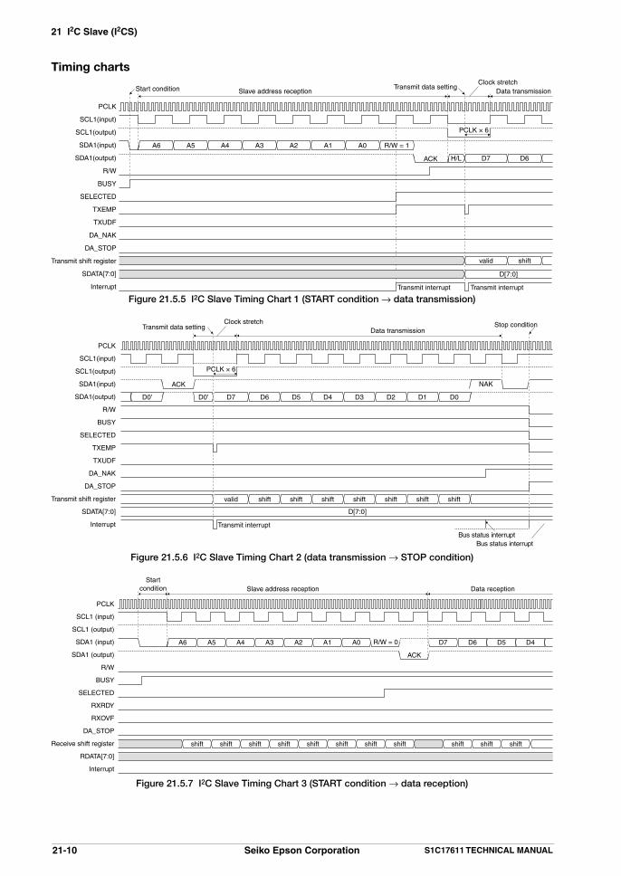
21 I2C Slave (I2CS)
21-10 Seiko Epson Corporation S1C17611 TECHNICAL MANUAL
Timing charts
PCLK
SCL1(input)
SCL1(output)
SDA1(input)
SDA1(output)
R/W
BUSY
SELECTED
TXEMP
TXUDF
DA_NAK
DA_STOP
Transmit shift register
SDATA[7:0]
Interrupt
A6
valid
D[7:0]
A5 A4 A3 A2 A1 A0 R/W = 1
D7H/L D6
Start condition Slave address reception Data transmissionClock stretch
Transmit data setting
Transmit interrupt Transmit interrupt
shift
ACK
PCLK × 6
Figure 21.5.5 I2C Slave Timing Chart 1 (START condition → data transmission)
D5 D4 D3 D2 D1 D0D0’ D6D7
valid
D0’
shift shift shift shift shift shift shift
ACK
PCLK
SCL1(input)
SCL1(output)
SDA1(input)
SDA1(output)
R/W
BUSY
SELECTED
TXEMP
TXUDF
DA_NAK
DA_STOP
Transmit shift register
SDATA[7:0]
Interrupt
Data transmissionStop condition
Bus status interruptBus status interrupt
NAK
D[7:0]
Transmit interrupt
PCLK × 6
Clock stretchTransmit data setting
Figure 21.5.6 I2C Slave Timing Chart 2 (data transmission → STOP condition)
shift shift shift shift shift shift shift shift
D7
PCLK
SCL1 (input)
SCL1 (output)
SDA1 (input)
SDA1 (output)
R/W
BUSY
SELECTED
RXRDY
RXOVF
DA_STOP
Receive shift register
RDATA[7:0]
Interrupt
A6 A5 A4 A3 A2 A1 A0 D6 D5 D4R/W = 0
Startcondition Slave address reception Data reception
shiftshiftshift
ACK
Figure 21.5.7 I2C Slave Timing Chart 3 (START condition → data reception)

21 I2C Slave (I2CS)
S1C17611 TECHNICAL MANUAL Seiko Epson Corporation 21-11
D[7:0] D[7:0]
D5 D4 D3 D2 D1 D0D6D0
shift shift shift shift shift shift shift
ACK
PCLK
SCL1(input)
SCL1(output)
SDA1(input)
SDA1(output)
R/W
BUSY
SELECTED
RXRDY
RXOVF
DA_STOP
Receive shift register
RDATA[7:0]
Interrupt
Data receptionData reception Clock stretch
Bus status interrupt
NAK
Receive interrupt Receive interrupt
shift
Stop conditionRead reception data
D7
Figure21.5.8 I2C Slave Timing Chart 4 (data reception → STOP condition)
21.6 I2C Slave InterruptThe I2C slave module can generate the following three types of interrupts: • Transmit interrupt • Receive interrupt • Bus status interrupt
Transmit interrupt Upon receipt of a read request (R/W bit = 1) from the master, an interrupt signal is output to the ITC if the
transmit data has not been set to SDATA[7:0](D[7:0]/I2CS_TRNS register), or if TXEMP (D3/I2CS_ASTAT register) has been set to 1. This interrupt can be used to write the transmit data to SDATA[7:0]. The interrupt signal is cleared after the transmit data is written to the SDATA.
* SDATA[7:0]: I2C Slave Transmit Data Bits in the I2C Slave Transmit Data (I2CS_TRNS) Register (D[7:0]/0x4360)* TXEMP: Transmit Data Empty Bit in the I2C Slave Access Status (I2CS_ASTAT) Register (D3/0x436a)
Set TXEMP_IEN (D0/I2CS_ICTL register) to 1 when using this interrupt. If TXEMP_IEN is set to 0 (default), an interrupt request by this cause will not be sent to the ITC.
* TXEMP_IEN: Transmit Interrupt Enable Bit in the I2C Slave Interrupt Control (I2CS_ICTL) Register (D0/0x436c)
Receive interrupt When the received data is loaded to RDATA[7:0] (D[7:0]/I2CS_RECV register), RXRDY (D4/I2CS_ASTAT
register) is set to 1 and an interrupt signal is output to the ITC. This interrupt can be used to read the received data from RDATA[7:0].
* RDATA[7:0]: I2C Slave Receive Data Bits in the I2C Slave Receive Data (I2CS_RECV) Register (D[7:0]/0x4362)* RXRDY: Receive Data Ready Bit in the I2C Slave Access Status (I2CS_ASTAT) Register (D4/0x436a)
Set RXRDY_IEN (D1/I2CS_ICTL register) to 1 when using this interrupt. If RXRDY_IEN is set to 0 (default), an interrupt request by this cause will not be sent to the ITC.
* RXRDY_IEN: Receive Interrupt Enable Bit in the I2C Slave Interrupt Control (I2CS_ICTL) Register (D1/0x436c)
Bus status interrupt The I2C slave module provides the status bits listed below to represent the transmit/receive and I2C bus statuses
(see Section 21.5 for details of each function).
1. ASDET: set to 1 when the slave address is detected by the asynchronous address detection function* ASDET: Async. Address Detection Status Bit in the I2C Slave Status (I2CS_STAT) Register (D2/0x4368)
2. TXUDF: set to 1 when a transmit operation has started before transmit data is written (when the clock stretch function is disabled)
* TXUDF: Transmit Data Underflow Bit in the I2C Slave Status (I2CS_STAT) Register (D5/0x4368)

21 I2C Slave (I2CS)
21-12 Seiko Epson Corporation S1C17611 TECHNICAL MANUAL
3. DA_NAK: set to 1 when a NAK is returned from the master during transmission* DA_NAK: NAK Receive Status Bit in the I2C Slave Status (I2CS_STAT) Register (D1/0x4368)
4. DMS: set to 1 when the SDA1 line status is different from transfer data* DMS: Output Data Mismatch Bit in the I2C Slave Status (I2CS_STAT) Register (D3/0x4368)
DMA will also be set to 1 when another slave device issues ACK to this I2C slave address (when ASDET_EN (D1/I2CS_CTL register) = 0).
Note: When the master device of the I2C bus, which has multiple slave devices connected including this IC, starts communication with another slave device, the I2C slave module of this IC issues NAK in response to the sent slave address. On the other hand, the selected slave device issues ACK. Therefore, DMS may be set due to a difference between the output value of this IC and the SDA1 line status. When SELECTED (D1/I2CS_ASTAT register) is set to 0, you can ignore DMS without a problem even if it is set to 1 as there is a difference in the response code (ACK/NAK) from the selected slave device.
When the I2C slave is placed into asynchronous address detection mode (ASDET_EN = 1), a DMS does not occur as in the condition above.
5. RXOVF: set to 1 when the next data has been received before the received data is read (the received data is overwritten) (when the clock stretch function is disabled)* RXOVF: Receive Data Overflow Bit in the I2C Slave Status (I2CS_STAT) Register (D5/0x4368)
6. BFREQ: set to 1 when a bus free request is accepted* BFREQ: Bus Free Request Bit in the I2C Slave Status (I2CS_STAT) Register (D4/0x4368)
7. DA_STOP: set to 1 if a STOP condition or a Repeated START condition is detected while this module is selected as the slave device.* DA_STOP: Stop Condition Detect Bit in the I2C Slave Status (I2CS_STAT) Register (D0/0x4368)
When one of the bits shown above is set to 1, BSTAT (D7/I2CS_STAT register) is set to 1 and an interrupt signal is output to the ITC. This interrupt can be used to perform an error or terminate handling.
* BSTAT: Bus Status Transition Bit in the I2C Slave Status (I2CS_STAT) Register (D7/0x4368)
Set BSTAT_IEN (D2/I2CS_ICTL register) to 1 when using this interrupt. If BSTAT_IEN is set to 0 (default), an interrupt request by this cause will not be sent to the ITC.
* BSTAT_IEN: Bus Status Interrupt Enable Bit in the I2C Slave Interrupt Control (I2CS_ICTL) Register (D2/0x436c)
ITC registers for I2C slave interrupts When a cause of interrupt that has been enabled occurs, the I2C slave module asserts the interrupt signal sent
to the ITC. To generate an I2C slave interrupt, set the interrupt level and enable the interrupt using the ITC registers. Table 21.6.1 shows the control bits for the I2C slave interrupt in the ITC.
Table 21.6.1 ITC RegistersCause of interrupt Interrupt level setup bits
Bus status/Transmit/Receive ILV13[2:0] (D[10:8]/ITC_ILV6)
ITC_ILV6 register (0x4312)
The ITC sends an interrupt request to the S1C17 Core. The interrupt level setup bits set the interrupt level (0 to 7) of the timer interrupt. If the same interrupt level is
set, the transmit/receive interrupt has highest priority and the bus status interrupt has lowest priority. An interrupt request to the S1C17 Core is accepted only when all the conditions described below are met.
• The interrupt enable bit of the I2C slave module (peripheral module) is set to 1. • The IE (Interrupt Enable) bit of the PSR (Processor Status Register) in the S1C17 Core is set to 1. • The I2C slave interrupt has a higher interrupt level than the value that is set in the IL field of the PSR. • No other cause of interrupt having higher priority, such as NMI, has occurred.
For details on these interrupt control registers, as well as the device operation when an interrupt has occurred, see “6. Interrupt Controller (ITC).”

21 I2C Slave (I2CS)
S1C17611 TECHNICAL MANUAL Seiko Epson Corporation 21-13
Interrupt vector The following shows the vector number and vector address for the I2C slave interrupt:
Table 21.6.2 I2C Slave Interrupt VectorsCause of interrupt Vector number Vector address
Bus status/Transmit/Receive 17 (0x11) TTBR + 0x44
21.7 Details of Control Registers
Table 21.7.1 List of I2C Slave RegistersAddress Register name Function
0x4360 I2CS_TRNS I2C Slave Transmit Data Write Register I2C slave transmit data0x4362 I2CS_RECV I2C Slave Receive Data Read Register I2C slave receive data0x4364 I2CS_SADRS I2C Slave Address Setup Register Sets the I2C slave address.
0x4366 I2CS_CTL I2C Slave Control Register Controls the I2C slave module.0x4368 I2CS_STAT I2C Slave Status Register Indicates the I2C slave bus status.0x436a I2CS_ASTAT I2C Slave Access Status Register Indicates the I2C slave access status.0x436c I2CS_ICTL I2C Slave Interrupt Control Register Controls the I2C slave interrupt.
The following describes each I2C slave register. These are all 16-bit registers.
Note: When setting the registers, be sure to write a 0, and not a 1, for all “reserved bits.”

21 I2C Slave (I2CS)
21-14 Seiko Epson Corporation S1C17611 TECHNICAL MANUAL
0x4360: I2C Slave Transmit Data Register (I2CS_TRNS)Register name Address Bit Name Function Setting Init. R/W Remarks
I2C Slave Transmit Data Register(I2CS_TRNS)
0x4360(16 bits)
D15–8 – reserved – – – 0 when being read.D7–0 SDATA[7:0] I2C slave transmit data 0–0xff 0x0 R/W
D[15:8] Reserved
D[7:0] SDATA[7:0]: I2C Slave Transmit Data Bits Set a transmit data in this register. (Default: 0x0) The serial-converted data is output from the SDA1 pin beginning with the MSB, in which the bits set to
0 are output as low-level signals. When the data set in this register is sent to the shift register, a transmit interrupt occurs. The next transmit data can be written to the register after that.
If the clock stretch function has been disabled, data must be written to this register within 7 cycles of the I2C slave clock (SCL1) after a transmit interrupt has been occurred.
However, when setting the first transmit data after this module has been selected as the slave device, follow the precautions described below.
When the clock stretch function is disabled (default) Transmit data must be written to SDATA[7:0] within 1 cycle of the I2C slave clock (SCL1) after
TXEMP has been set to 1. This time is not enough for data preparation, so write transmit data before TXEMP has been set to 1. If the previous transmit data is still stored in SDATA[7:0], it is overwritten with the new data to be transferred. Therefore, the clear operation (see below) using TBUF_CLR is unnecessary.
When the clock stretch function is enabled The master device is placed into wait status by the clock stretch function, so transmit data can be
written after TXEMP is set. However, if the previous transmit data is still stored in SDATA[7:0], it will be sent immediately after TXEMP has been set. In order to avoid this problem, clear the I2CS_TRNS register using TBUF_CLR (D8/I2CS_CTL register) before this module is selected as the slave device. The I2CS_TRNS register is cleared by writing 1 to TBUF_CLR then writing 0 to it.
It is not necessary to clear the I2CS_TRNS register if the first transmit data is written before TXEMP has been set.

21 I2C Slave (I2CS)
S1C17611 TECHNICAL MANUAL Seiko Epson Corporation 21-15
0x4362: I2C Slave Receive Data Register (I2CS_RECV)Register name Address Bit Name Function Setting Init. R/W Remarks
I2C Slave Receive Data Register(I2CS_RECV)
0x4362(16 bits)
D15–8 – reserved – – – 0 when being read.D7–0 RDATA[7:0] I2C slave receive data 0–0xff 0x0 R
D[15:8] Reserved
D[7:0] RDATA[7:0]: I2C Slave Receive Data Bits The received data can be read from this register. (Default: 0x0) The serial data input from the SDA1 pin is converted into parallel data beginning with the MSB, with
the high-level signals changed to 1 and the low-level signals changed to 0. The resulting data is stored in this register.
When a receive operation is completed and the data received in the shift register is loaded to this register, RXRDY (D4/I2CS_ASTAT register) is set and a receive interrupt occurs. Thereafter, the data can be read out.
When the clock stretch function has been disabled, data must be read from this register within 7 cycles of the I2C slave clock (SCL1) after RXRDY is set to 1. If the next data has been received without reading the received data, this register will be overwritten with the newly received data.
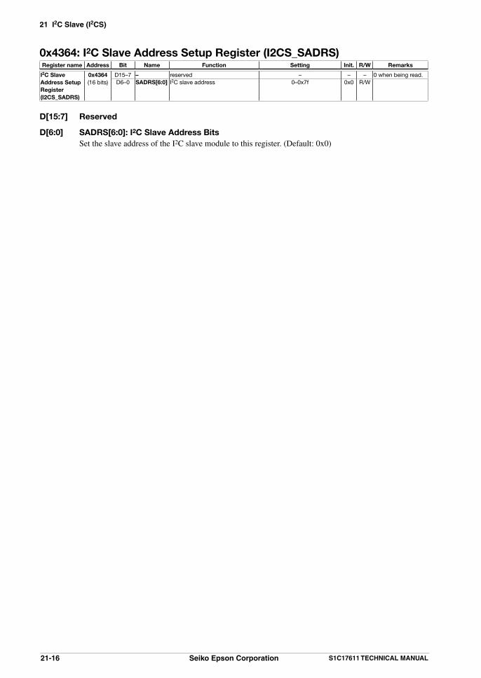
21 I2C Slave (I2CS)
21-16 Seiko Epson Corporation S1C17611 TECHNICAL MANUAL
0x4364: I2C Slave Address Setup Register (I2CS_SADRS)Register name Address Bit Name Function Setting Init. R/W Remarks
I2C Slave Address Setup Register(I2CS_SADRS)
0x4364(16 bits)
D15–7 – reserved – – – 0 when being read.D6–0 SADRS[6:0] I2C slave address 0–0x7f 0x0 R/W
D[15:7] Reserved
D[6:0] SADRS[6:0]: I2C Slave Address Bits Set the slave address of the I2C slave module to this register. (Default: 0x0)

21 I2C Slave (I2CS)
S1C17611 TECHNICAL MANUAL Seiko Epson Corporation 21-17
0x4366: I2C Slave Control Register (I2CS_CTL)Register name Address Bit Name Function Setting Init. R/W Remarks
I2C Slave Control Register(I2CS_CTL)
0x4366(16 bits)
D15–9 – reserved – – – 0 when being read.D8 TBUF_CLR I2CS_TRNS register clear 1 Clear state 0 Normal 0 R/WD7 I2C_EN I2C slave enable 1 Enable 0 Disable 0 R/WD6 SOFTRESET Software reset 1 Reset 0 Cancel 0 R/WD5 NAK_ANS NAK answer 1 NAK 0 ACK 0 R/WD4 BFREQ_EN Bus free request enable 1 Enable 0 Disable 0 R/WD3 CLKSTR_EN Clock stretch On/Off 1 On 0 Off 0 R/WD2 NF_EN Noise filter On/Off 1 On 0 Off 0 R/WD1 ASDET_EN Async.address detection On/Off 1 On 0 Off 0 R/WD0 COM_MODE I2C slave communication mode 1 Active 0 Standby 0 R/W NAK responsee
when standby
D[15:9] Reserved
D8 TBUF_CLR: I2CS_TRNS Register Clear Bit Clears the I2CS_TRNS register (0x4360). 1 (R/W): Clear state 0 (R/W): Normal state (clear state cancellation) (default)
When TBUF_CLR is set to 1, the I2CS_TRNS register enters clear state. After that writing 0 to TBUF_CLR returns the I2CS_TRNS register to normal state. It is not necessary to insert a waiting time between writing 1 and 0.
If a new transmission is started when the I2CS_TRNS register still stores data for the previous transmission that has already finished, the data will be sent when TXEMP (D3/I2CS_ASTAT register) is set. In order to avoid this problem, clear the I2CS_TRNS register using TBUF_CLR before starting transmission (before slave selection). The clear operation is not required if transmit data is written to the I2CS_TRNS register before TXEMP is set to 1.
Data can be written to the I2CS_TRNS register even if it is placed into clear state (TBUF_CLR = 1). However, this writing does not reset TXEMP to 0. Note that TXEMP is not reset to 0 when TBUF_CLR is set back to 0. Therefore, data must be written to the I2CS_TRNS register when TBUF_CLR = 0.
D7 I2C_EN: I2C Slave Enable Bit Enables/disables operation of the I2C slave module. 1 (R/W): Enable 0 (R/W): Disable (default)
When I2C_EN is set to 1, the I2C slave module is activated and data transfer is enabled. When I2C_EN is set to 0, the I2C slave module goes off.
D6 SOFTRESET: Software Reset Bit Resets the I2C slave module. 1 (R/W): Reset 0 (R/W): Cancel reset state (default)
To reset the I2C slave module, write 1 to SOFTRESET to place the I2C slave module into reset status, then write 0 to SOFTRESET to release it from reset status. It is not necessary to insert a waiting time between writing 1 and 0. The I2C slave module initializes the I2C slave communication process and put the SDA1 and SCL1 pins into high-impedance state to be ready to detect a start condition. Furthermore, the I2C slave control bits except for SOFTRESET are initialized. Perform the software reset in the initial setting process before staring communication.
D5 NAK_ANS: NAK Answer Bit Specifies the acknowledge bit to be sent after data reception. 1 (R/W): NAK 0 (R/W): ACK (default)
When the 8-bit data is received, the I2C slave module sends back an ACK (SDA1 = low) or a NAK (SDA1 = Hi-Z). Either ACK or NAK should be specified using NAK_ANS within 7 cycles of the I2C slave clock (SCL1) after RXRDY has been set to 1 by receiving the previous data.
21 I2C Slave (I2CS)
21-18 Seiko Epson Corporation S1C17611 TECHNICAL MANUAL
D4 BFREQ_EN: Bus Free Request Enable Bit Enables/disables I2C bus free requests by inputting a low pulse to the #BFR pin. 1 (R/W): Enable 0 (R/W): Disable (default)
To accept I2C bus free requests, set BFREQ_EN to 1. When a bus free request is accepted, BFREQ (D4/I2CS_STAT register) is set to 1. This initializes the I2C slave communication process and puts the SDA1 and SCL1 pins into high-impedance state. The control registers will not be initialized in this process.
When BFREQ_EN is set to 0, low pulse inputs to the #BFR pin are ignored and BFREQ is not set to 1.
D3 CLKSTR_EN: Clock Stretch On/Off Bit Turns the clock stretch function on or off. 1 (R/W): On 0 (R/W): Off (default)
After data and ACK are transmitted or received, the slave device may issue a wait request to the master device until it is ready to transmit/receive by pulling the SCL line down to low. The I2C slave module supports this clock stretch function. The master device enters a standby state until the wait request is canceled (the SCL line goes high). When using the clock stretch function, set CLKSTR_EN to 1 before starting data communication.
D2 NF_EN: Noise Filter On/Off Bit Turns the noise filter on or off. 1 (R/W): On 0 (R/W): Off (default)
The I2C slave module contains a function to remove noise from the SDA1 and SCL1 input signals. This function is enabled by setting NF_EN to 1.
D1 ASDET_EN: Async. Address Detection On/Off Bit Turns the asynchronous address detection function on or off. 1 (R/W): On 0 (R/W): Off (default)
The I2C slave module operation clock (PCLK) frequency must be set eight-times or higher than the transfer rate during data transfer. However, the PCLK frequency can be lowered to reduce current consumption if no other processing is required during standby for data transfer. The asynchronous address detection function is provided to detect the I2C slave address sent from the master in this status. This function is enabled by setting ASDET_EN to 1. If the slave address sent from the master has matched with one that has been set in this I2C slave module when the asynchronous address detection function has been enabled, the I2C slave module generates a bus status interrupt and returns NAK to the I2C master to request for resending the slave address. Set the PCLK frequency to eight-times or higher than the transfer rate and reset ASDET_EN to 0 in the interrupt handler routine. Data transfer will be able to resume normally after the master retries transmission. After the master generates a STOP condition to put the I2C bus into free status, the asynchronous address detection function can be enabled again to lower the operating speed.
Notes: • When the asynchronous address detection function is enabled, the I2C signals are input without passing through the noise filter. Therefore, the slave address may not be detected in a high-noise environment.
• When the asynchronous address detection function is enabled, data transfer cannot be performed even if the PCLK frequency is eight-times or higher than the transfer rate. Be sure to disable the asynchronous address detection function during normal operation.
D0 COM_MODE: I2C Slave Communication Mode Bit Enables/disables data communication. 1 (R/W): Enable

21 I2C Slave (I2CS)
S1C17611 TECHNICAL MANUAL Seiko Epson Corporation 21-19
0 (R/W): Disable (default)
Set COM_MODE to 1 to enable data communication after setting the I2C_EN bit (D7) to 1 to enable I2C slave operation. When COM_MODE is 0, the I2C slave module does not send back a response if the master has sent the slave address of this module (it is regarded as that the I2C module has returned a NAK to the master).
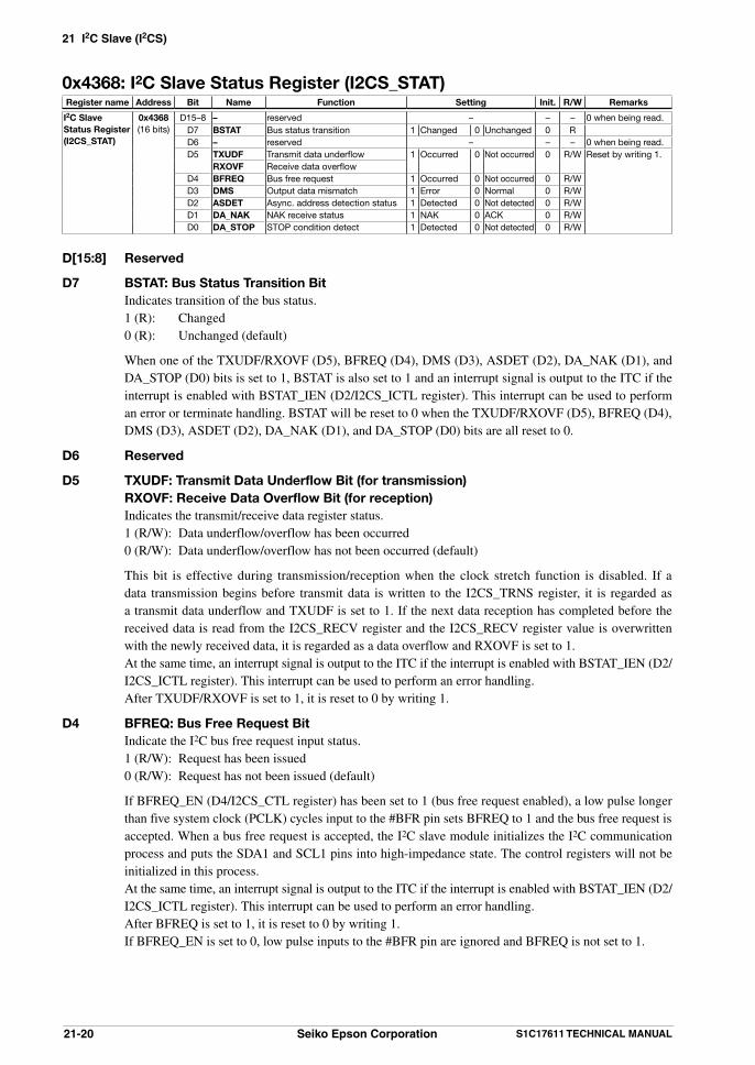
21 I2C Slave (I2CS)
21-20 Seiko Epson Corporation S1C17611 TECHNICAL MANUAL
0x4368: I2C Slave Status Register (I2CS_STAT)Register name Address Bit Name Function Setting Init. R/W Remarks
I2C SlaveStatus Register(I2CS_STAT)
0x4368(16 bits)
D15–8 – reserved – – – 0 when being read.D7 BSTAT Bus status transition 1 Changed 0 Unchanged 0 RD6 – reserved – – – 0 when being read.D5 TXUDF Transmit data underflow 1 Occurred 0 Not occurred 0 R/W Reset by writing 1.
RXOVF Receive data overflowD4 BFREQ Bus free request 1 Occurred 0 Not occurred 0 R/WD3 DMS Output data mismatch 1 Error 0 Normal 0 R/WD2 ASDET Async. address detection status 1 Detected 0 Not detected 0 R/WD1 DA_NAK NAK receive status 1 NAK 0 ACK 0 R/WD0 DA_STOP STOP condition detect 1 Detected 0 Not detected 0 R/W
D[15:8] Reserved
D7 BSTAT: Bus Status Transition Bit Indicates transition of the bus status. 1 (R): Changed 0 (R): Unchanged (default)
When one of the TXUDF/RXOVF (D5), BFREQ (D4), DMS (D3), ASDET (D2), DA_NAK (D1), and DA_STOP (D0) bits is set to 1, BSTAT is also set to 1 and an interrupt signal is output to the ITC if the interrupt is enabled with BSTAT_IEN (D2/I2CS_ICTL register). This interrupt can be used to perform an error or terminate handling. BSTAT will be reset to 0 when the TXUDF/RXOVF (D5), BFREQ (D4), DMS (D3), ASDET (D2), DA_NAK (D1), and DA_STOP (D0) bits are all reset to 0.
D6 Reserved
D5 TXUDF: Transmit Data Underflow Bit (for transmission) RXOVF: Receive Data Overflow Bit (for reception) Indicates the transmit/receive data register status. 1 (R/W): Data underflow/overflow has been occurred 0 (R/W): Data underflow/overflow has not been occurred (default)
This bit is effective during transmission/reception when the clock stretch function is disabled. If a data transmission begins before transmit data is written to the I2CS_TRNS register, it is regarded as a transmit data underflow and TXUDF is set to 1. If the next data reception has completed before the received data is read from the I2CS_RECV register and the I2CS_RECV register value is overwritten with the newly received data, it is regarded as a data overflow and RXOVF is set to 1.
At the same time, an interrupt signal is output to the ITC if the interrupt is enabled with BSTAT_IEN (D2/I2CS_ICTL register). This interrupt can be used to perform an error handling.
After TXUDF/RXOVF is set to 1, it is reset to 0 by writing 1.
D4 BFREQ: Bus Free Request Bit Indicate the I2C bus free request input status. 1 (R/W): Request has been issued 0 (R/W): Request has not been issued (default)
If BFREQ_EN (D4/I2CS_CTL register) has been set to 1 (bus free request enabled), a low pulse longer than five system clock (PCLK) cycles input to the #BFR pin sets BFREQ to 1 and the bus free request is accepted. When a bus free request is accepted, the I2C slave module initializes the I2C communication process and puts the SDA1 and SCL1 pins into high-impedance state. The control registers will not be initialized in this process.
At the same time, an interrupt signal is output to the ITC if the interrupt is enabled with BSTAT_IEN (D2/I2CS_ICTL register). This interrupt can be used to perform an error handling.
After BFREQ is set to 1, it is reset to 0 by writing 1. If BFREQ_EN is set to 0, low pulse inputs to the #BFR pin are ignored and BFREQ is not set to 1.

21 I2C Slave (I2CS)
S1C17611 TECHNICAL MANUAL Seiko Epson Corporation 21-21
D3 DMS: Output Data Mismatch Bit Represents the results of comparison between output data and SDA1 line status. 1 (R/W): Error has been occurred 0 (R/W): Error has not been occurred (default)
The SDA1 line status during data transmission is input in the module and is compare with the output data. The comparison results are set to DMS. DMS is set to 0 when data is output correctly. If the SDA1 line status is different from the output data, DMS is set to 1. This may be caused by a low pull-up resistor value or another device that is controlling the SDA1 line. At the same time, an interrupt signal is output to the ITC if the interrupt is enabled with BSTAT_IEN (D2/I2CS_ICTL register). This interrupt can be used to perform an error handling.
After DMS is set to 1, it is reset to 0 by writing 1.
Note: When the master device of the I2C bus, which has multiple slave devices connected including this IC, starts communication with another slave device, the I2C slave module of this IC issues NAK in response to the sent slave address. On the other hand, the selected slave device issues ACK. Therefore, DMS may be set due to a difference between the output value of this IC and the SDA1 line status. When SELECTED (D1/I2CS_ASTAT register) is set to 0, you can ignore DMS without a problem even if it is set to 1 as there is a difference in the response code (ACK/NAK) from the selected slave device.
When the I2C slave is placed into asynchronous address detection mode (ASDET_EN = 1), a DMS does not occur as in the condition above.
D2 ASDET: Async. Address Detection Status Bit Indicates the asynchronous address detection status. 1 (R/W): Detected 0 (R/W): Not detected (default)
The I2C slave module operation clock (PCLK) frequency must be set eight-times or higher than the transfer rate during data transfer. However, the PCLK frequency can be lowered to reduce current consumption if no other processing is required during standby for data transfer. The asynchronous address detection function is provided to detect the I2C slave address sent from the master in this status. ASDET is set to 1 if the slave address of the I2C slave module is detected when the asynchronous address detection function has been enabled by setting ASDET_EN (D1/I2CS_CTL register). The I2C slave module returns a NAK to the I2C master to request for resending the slave address. At the same time, an interrupt signal is output to the ITC if the interrupt is enabled with BSTAT_IEN (D2/I2CS_ICTL register). Set the PCLK frequency to eight-times or higher than the transfer rate and disable the asynchronous address detection function. Data transfer will be able to resume normally after the master retries transmission.
After ASDET is set to 1, it is reset to 0 by writing 1.
D1 DA_NAK: NAK Receive Status Bit Indicates the acknowledge bit returned from the master. 1 (R/W): NAK 0 (R/W): ACK (default)
DA_NAK is set to 0 when an ACK is returned from the master after the 8-bit data has been sent. This indicates that the master could receive data. If DA_NAK is 1, it indicates that the master could not receive data or the master terminates data reception. At the same time DA_NAK is set to 1, an interrupt signal is output to the ITC if the interrupt is enabled with BSTAT_IEN (D2/I2CS_ICTL register). This interrupt can be used to perform an error handling.
After DA_NAK is set to 1, it is reset to 0 by writing 1.

21 I2C Slave (I2CS)
21-22 Seiko Epson Corporation S1C17611 TECHNICAL MANUAL
D0 DA_STOP: Stop Condition Detect Bit Indicates that a STOP condition or a Repeated START condition is detected. 1 (R/W): Detected 0 (R/W): Not detected (default)
If a STOP condition or a Repeated START condition is detected while the I2C slave module is selected as the slave device (SELECTED (D1/I2CS_ASTAT register) = 1), the I2C slave module sets DA_STOP to 1. At the same time, it initializes the I2C communication process.
When DA_STOP is set to 1, an interrupt signal is output to the ITC if the interrupt is enabled with BSTAT_IEN (D2/I2CS_ICTL register). This interrupt can be used to perform a terminate handling.
After DA_STOP is set to 1, it is reset to 0 by writing 1.

21 I2C Slave (I2CS)
S1C17611 TECHNICAL MANUAL Seiko Epson Corporation 21-23
0x436a: I2C Slave Access Status Register (I2CS_ASTAT)Register name Address Bit Name Function Setting Init. R/W Remarks
I2C Slave Access Status Register(I2CS_ASTAT)
0x436a(16 bits)
D15–5 – reserved – – – 0 when being read.D4 RXRDY Receive data ready 1 Ready 0 Not ready 0 RD3 TXEMP Transmit data empty 1 Empty 0 Not empty 0 RD2 BUSY I2C bus status 1 Busy 0 Free 0 RD1 SELECTED I2C slave select status 1 Selected 0 Not selected 0 RD0 R/W Read/write direction 1 Output 0 Input 0 R
D[15:5] Reserved
D4 RXRDY: Receive Data Ready Bit Indicates that the received data is ready to read. 1 (R): Received data ready 0 (R): No received data (default)
When the received data is loaded to the I2CS_RECV register, RXRDY is set to 1. At the same time, an interrupt signal is output to the ITC if the interrupt is enabled with RXRDY_IEN (D1/I2CS_ICTL register). This interrupt can be used to read the received data from the I2CS_RECV register.
After RXRDY is set to 1, it is reset to 0 when the I2CS_RECV register is read.
D3 TXEMP: Transmit Data Empty Bit Indicates that transmit data can be written. 1 (R): Transmit data empty 0 (R): Transmit data still stored (default)
When the transmit data written to the I2CS_TRNS register is sent, TXEMP is set to 1. At the same time, an interrupt signal is output to the ITC if the interrupt is enabled with TXEMP_IEN (D0/I2CS_ICTL register). This interrupt can be used to write the next transmit data to the I2CS_TRNS register.
After TXEMP is set to 1, it is reset to 0 when data is written to the I2CS_TRNS register.
D2 BUSY: I2C Bus Status Bit Indicates the I2C bus status. 1 (R): Bus busy status 0 (R): Bus free status (default)
When the I2C slave module detects a START condition or detects that the SCL1 or SDA1 signal goes low, BUSY is set to 1 to indicate that the I2C bus enters busy status. The slave select status whether this module is selected as the slave device or not does not affect the BUSY status. After BUSY is set to 1, it is reset to 0 when a STOP condition is detected.
D1 SELECTED: I2C Slave Select Status Bit Indicates that this module is selected as the I2C slave device. 1 (R): Selected 0 (R): Not selected (default)
When the slave address that is set in this module is received, SELECTED is set to 1 to indicate that this module is selected as the I2C slave device. After SELECTED is set to 1, it is reset to 0 when a STOP condition or a Repeated START condition is detected.
D0 R/W: Read/Write Direction Bit Represents the transfer direction bit value. 1 (R): Output (master read operation) 0 (R): Input (master write operation) (default)
The transfer direction bit value that has been received with the slave address is set to R/W. Use R/W to select the transmit- or receive-handling.

21 I2C Slave (I2CS)
21-24 Seiko Epson Corporation S1C17611 TECHNICAL MANUAL
0x436c: I2C Slave Interrupt Control Register (I2CS_ICTL)Register name Address Bit Name Function Setting Init. R/W Remarks
I2C Slave Interrupt Control Register(I2CS_ICTL)
0x436c(16 bits)
D15–3 – reserved – – – 0 when being read.D2 BSTAT_IEN Bus status interrupt enable 1 Enable 0 Disable 0 R/WD1 RXRDY_IEN Receive interrupt enable 1 Enable 0 Disable 0 R/WD0 TXEMP_IEN Transmit interrupt enable 1 Enable 0 Disable 0 R/W
D[15:3] Reserved
D2 BSTAT_IEN: Bus Status Interrupt Enable Bit Enables/disables the bus status interrupt. 1 (R/W): Enable 0 (R/W): Disable (default)
When BSTAT_IEN is set to 1, I2C slave bus status interrupt requests to the ITC are enabled. A bus status interrupt request occurs when BSTAT (D7/I2CS_STAT register) is set to 1. (See description of BSTAT.)
When BSTAT_IEN is set to 0, a bus status interrupt will not be generated.
D1 RXRDY_IEN: Receive Interrupt Enable Bit Enables/disables the I2C slave receive interrupt. 1 (R/W): Enable 0 (R/W): Disable (default)
When RXRDY_IEN is set to 1, I2C slave receive interrupt requests to the ITC are enabled. A receive interrupt request occurs when the data received in the shift register is loaded to the I2CS_RECV register (receive operation completed).
When RXRDY_IEN is set to 0, a receive interrupt will not be generated.
D0 TXEMP_IEN: Transmit Interrupt Enable Bit Enables/disables the I2C slave transmit interrupt. 1 (R/W): Enable 0 (R/W): Disable (default)
When TXEMP_IEN is set to 1, I2C slave transmit interrupt requests to the ITC are enabled. A transmit interrupt request occurs when the data written to the I2CS_TRNS register is transferred to the shift register.
When TXEMP_IEN is set to 0, a transmit interrupt will not be generated.

21 I2C Slave (I2CS)
S1C17611 TECHNICAL MANUAL Seiko Epson Corporation 21-25
21.8 Precautions• The I2C slave module operating clock (PCLK) frequency must be set to eight-times or higher than the transfer
rate during data transfer.
• When the asynchronous address detection function is enabled, the I2C signals are input without passing through the noise filter. Therefore, the slave address may not be detected in a high-noise environment.
• When the asynchronous address detection function is enabled, data transfer cannot be performed even if the PCLK frequency is eight-times or higher than the transfer rate. Be sure to disable the asynchronous address detection function during normal operation.
• When the master device of the I2C bus, which has multiple slave devices connected including this IC, starts communication with another slave device, the I2C slave module of this IC issues NAK in response to the sent slave address. On the other hand, the selected slave device issues ACK. Therefore, DMS may be set due to a difference between the output value of this IC and the SDA1 line status. When SELECTED (D1/I2CS_ASTAT register) is set to 0, you can ignore DMS without a problem even if it is set to 1 as there is a difference in the response code (ACK/NAK) from the selected slave device.
When the I2C slave is placed into asynchronous address detection mode (ASDET_EN = 1), a DMS does not occur as in the condition above.
• When setting the first transmit data after this module has been selected as the slave device, follow the precautions described below.
When the clock stretch function is disabled (default) Transmit data must be written to SDATA[7:0] within 1 cycle of the I2C slave clock (SCL1) after TXEMP
has been set to 1. This time is not enough for data preparation, so write transmit data before TXEMP has been set to 1. If the previous transmit data is still stored in SDATA[7:0], it is overwritten with the new data to be transferred. Therefore, the clear operation (see below) using TBUF_CLR is unnecessary.
When the clock stretch function is enabled The master device is placed into wait status by the clock stretch function, so transmit data can be written
after TXEMP is set. However, if the previous transmit data is still stored in SDATA[7:0], it will be sent immediately after TXEMP has been set. In order to avoid this problem, clear the I2CS_TRNS register using TBUF_CLR (D8/I2CS_CTL register) before this module is selected as the slave device. The I2CS_TRNS register is cleared by writing 1 to TBUF_CLR then writing 0 to it.
It is not necessary to clear the I2CS_TRNS register if the first transmit data is written before TXEMP has been set.
• When the clock stretch function has been disabled, transmit data/receive data must be written/read within the time shown below.
During data transmission: Within 7 cycles of the I2C slave clock (SCL1) after TXEMP is set (a transmit interrupt occurs) (See the precaution above for the first transmit data after slave selection.)
During data reception: Within 7 cycles of the I2C slave clock (SCL1) after RXRDY is set (a receive interrupt occurs) Set the NAK transmit settings using NAK_ANS (D5/I2CS_CTL register) within this period.
• When using the conditions listed below, the master device needs the wait time at least 33 μs before transmitting the address to the different slaves.
1. Setting the communication rate at least 320 kbps. 2. Using the asynchronous address detection. 3. The standby communication is done by using OSC1 to the operation clock (PCLK). 4. When this IC replies NAK to the address transmitted by the master device.

22 LCD Driver (LCD8)
S1C17611 TECHNICAL MANUAL Seiko Epson Corporation 22-1
22 LCD Driver (LCD8)
22.1 LCD Driver ConfigurationThe S1C17611 incorporates a LCD driver capable of driving LCD panels of up to 64 segments (7 segments x 8 common) in size. Figure 22.1.1 illustrates the LCD driver and driver power supply configuration.
COM0 to COM7SEG0 to SEG7
LCLKHSCLK
OSC1
Division circuit(1/32 to 1/512) Gate
LC[3:0]
DSPAR
DSPC[1:0]
LDUTY[1:0]FRMCNT[1:0]
DSPREVSEGREVCOMREV
OSC
To ITC Frame interrupt request
VC1 to VC3LCDconstant-
voltage circuitLCD contrastadjustment
circuit
Display memory
Drive control circuit
Clock control circuit
FRMIEInterrupt
control circuit
Power supply circuit
LCD driver
LHVLD
VCSEL
Figure 22.1.1: LCD driver and driver power supply configuration

22 LCD Driver (LCD8)
22-2 Seiko Epson Corporation S1C17611 TECHNICAL MANUAL
22.2 LCD Power SupplyLCD driver voltages VC1 to VC3 are generated using the internal chip LCD constant-voltage circuit. No external power supply is needed. For more information on the LCD power supply, see “4 Power Supply Voltage.”

22 LCD Driver (LCD8)
S1C17611 TECHNICAL MANUAL Seiko Epson Corporation 22-3
22.3 LCD ClockFigure 22.3.1 illustrates the LCD clock feed system.
LCD driver
Standard clockLCLK
Frame signalOSC1
HSCLK Division circuit(1/32 to 1/512)
Divisioncircuit
LCKEN
LCKSRC
FRMCNT
LCKDV[2:0]
OSC module
Division circuit(1/16)
Figure 22.3.1: LCD clock system
22.3.1 LCD Operating Clock
The LCD driver operation clock (LCLK) is generated by the LCD clock generator within the OSC module. For more information on the OSC module, see “7 Oscillator Circuit (OSC).”
22.3.2 Frame Signal
The frame signal is generated by dividing LCLK according to the value of FRMCNT. The frame frequency is as shown below. The time for 1 frame shown in Figures 22.4.1 to 22.4.5 is the frame frequency.
When OSC1 (32.768 kHz typ.) is selected as the LCD clock source
Table 22.3.2.1: Frame frequency when OSC1 (32.768 kHz typ.) is selected as the LCD clock source
Division setting (FRMCNT)
Duty setting (LDUTY)0x0 0x1 0x2 0x3
0x4 (1/8 duty) 128Hz 64Hz 48.19Hz 32Hz0x3 (1/4 duty) 128Hz 64Hz 48.19Hz 32Hz0x2 (1/3 duty) 130.04Hz 65.02Hz 48.12Hz 32.5Hz0x1 (1/2 duty) 128Hz 64Hz 48.19Hz 32Hz0x0 (Static) 128Hz 64Hz 48.19Hz 32Hz
(Default: LDUTY=0x4, FRMCNT=0x1)
When HSCLK is selected as the LCD clock source
Table 22.3.2.2: Frame frequency when HSCLK is selected as the LCD clock source
Division setting (FRMCNT)
Duty setting (LDUTY)0x0 0x1 0x2 0x3
0x4 (1/8 duty)fHSCLK/256 × LCKDV Hz
fHSCLK/512 × LCKDV Hz
fHSCLK/680 × LCKDV Hz
fHSCLK/1024 × LCKDV Hz
0x3 (1/4 duty)fHSCLK/256 × LCKDV Hz
fHSCLK/512 × LCKDV Hz
fHSCLK/680 × LCKDV Hz
fHSCLK/1024 × LCKDV Hz
0x2 (1/3 duty)fHSCLK/252 × LCKDV Hz
fHSCLK/504 × LCKDV Hz
fHSCLK/681 × LCKDV Hz
fHSCLK/1008 × LCKDV Hz
0x1 (1/2 duty)fHSCLK/256 × LCKDV Hz
fHSCLK/512 × LCKDV Hz
fHSCLK/680 × LCKDV Hz
fHSCLK/1024 × LCKDV Hz
0x0 (Static)fHSCLK/256 × LCKDV Hz
fHSCLK/512 × LCKDV Hz
fHSCLK/680 × LCKDV Hz
fHSCLK/1024 × LCKDV Hz
(Default: LDUTY=0x4, FRMCNT=0x1)
fHSCLK: HSCLK (IOSC or OSC3) clock frequency [Hz] LCKDV: HSCLK division ratio 1/32 to 1/512
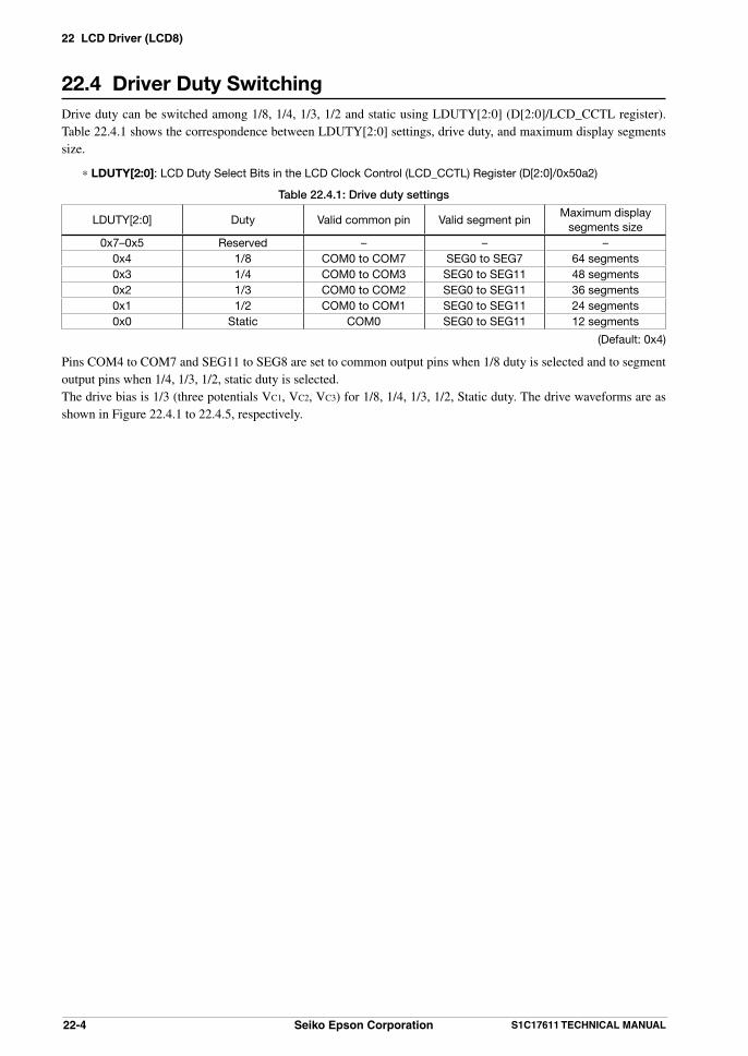
22 LCD Driver (LCD8)
22-4 Seiko Epson Corporation S1C17611 TECHNICAL MANUAL
22.4 Driver Duty SwitchingDrive duty can be switched among 1/8, 1/4, 1/3, 1/2 and static using LDUTY[2:0] (D[2:0]/LCD_CCTL register). Table 22.4.1 shows the correspondence between LDUTY[2:0] settings, drive duty, and maximum display segments size.
* LDUTY[2:0]: LCD Duty Select Bits in the LCD Clock Control (LCD_CCTL) Register (D[2:0]/0x50a2)
Table 22.4.1: Drive duty settings
LDUTY[2:0] Duty Valid common pin Valid segment pinMaximum display
segments size0x7–0x5 Reserved – – –
0x4 1/8 COM0 to COM7 SEG0 to SEG7 64 segments0x3 1/4 COM0 to COM3 SEG0 to SEG11 48 segments0x2 1/3 COM0 to COM2 SEG0 to SEG11 36 segments0x1 1/2 COM0 to COM1 SEG0 to SEG11 24 segments0x0 Static COM0 SEG0 to SEG11 12 segments
(Default: 0x4)
Pins COM4 to COM7 and SEG11 to SEG8 are set to common output pins when 1/8 duty is selected and to segment output pins when 1/4, 1/3, 1/2, static duty is selected.The drive bias is 1/3 (three potentials VC1, VC2, VC3) for 1/8, 1/4, 1/3, 1/2, Static duty. The drive waveforms are as shown in Figure 22.4.1 to 22.4.5, respectively.

22 LCD Driver (LCD8)
S1C17611 TECHNICAL MANUAL Seiko Epson Corporation 22-5
− VDD
− VSS
− VC3
− VC2
− VC1
− VSS
− VC3
− VC2
− VC1
− VSS
− VC3
− VC2
− VC1
− VSS
− VC3
− VC2
− VC1
− VSS
− VC3
− VC2
− VC1
− VSS
− VC3
− VC2
− VC1
− VSS
− VC3
− VC2
− VC1
− VSS
− VC3
− VC2
− VC1
− VSS
− VC2
− VC1
− VC3
− VC2
− VC1
− VSS
− VC3
− VC2
− VC1
− VSS
− VC3
− VC2
− VC1
− VSS
− VC3
− VC2
− VC1
− VSS
− VC3
− VC2
− VC1
− VSS
COM0
FR
COM1
COM2
COM3
COM4
COM5
COM6
COM7
COM01234567
0 1 2 3 4 5 6 7 0 1 2 3 4 5 6 7
SEG0 to SEG15
LCD ON Status
ONOFF
1 Frame
Frame interrupt Frame interrupt
SEG0 to SEG7
Figure 22.4.1: 1/8 duty drive waveform

22 LCD Driver (LCD8)
22-6 Seiko Epson Corporation S1C17611 TECHNICAL MANUAL
− VDD
− VSS
− VC3
− VC2
− VC1
− VSS
− VC3
− VC2
− VC1
− VSS
− VC3
− VC2
− VC1
− VSS
− VC3
− VC2
− VC1
− VSS
− VC2
− VC1
− VC3
− VC2
− VC1
− VSS
− VC3
− VC2
− VC1
− VSS
− VC3
− VC2
− VC1
− VSS
− VC3
− VC2
− VC1
− VSS
− VC3
− VC2
− VC1
− VSS
COM0
FR
COM1
COM2
COM3
0 1 2 3 0 1 2 3
COM0123
SEG0 to SEG11
1 Frame
Frameinterrupt
Frameinterrupt
SEG0 to SEG19
ONOFF
LCD ON Status
Figure 22.4.2: 1/4 duty drive waveform
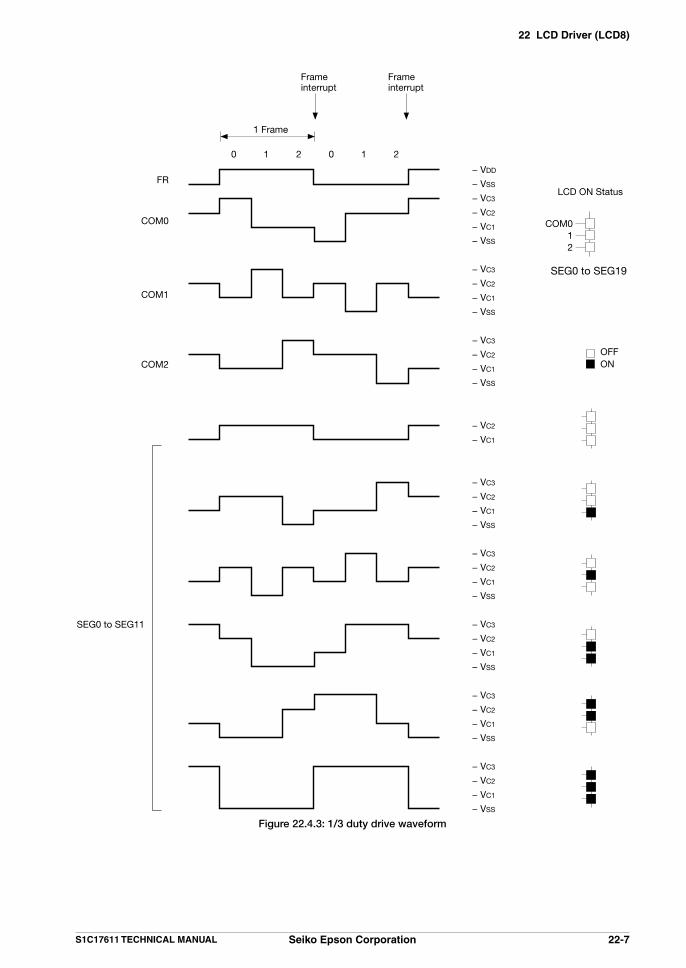
22 LCD Driver (LCD8)
S1C17611 TECHNICAL MANUAL Seiko Epson Corporation 22-7
− VDD
− VSS
− VC3
− VC2
− VC1
− VSS
− VC3
− VC2
− VC1
− VSS
− VC3
− VC2
− VC1
− VSS
− VC2
− VC1
− VC3
− VC2
− VC1
− VSS
− VC3
− VC2
− VC1
− VSS
− VC3
− VC2
− VC1
− VSS
− VC3
− VC2
− VC1
− VSS
− VC3
− VC2
− VC1
− VSS
COM0
FR
COM1
COM2
0 1 2 0 1 2
COM012
SEG0 to SEG11
1 Frame
Frameinterrupt
Frameinterrupt
ONOFF
SEG0 to SEG19
LCD ON Status
Figure 22.4.3: 1/3 duty drive waveform

22 LCD Driver (LCD8)
22-8 Seiko Epson Corporation S1C17611 TECHNICAL MANUAL
− VDD
− VSS
− VC3
− VC2
− VC1
− VSS
− VC3
− VC2
− VC1
− VSS
− VC2
− VC1
− VC3
− VC2
− VC1
− VSS
− VC3
− VC2
− VC1
− VSS
− VC3
− VC2
− VC1
− VSS
COM0
FR
COM1
0 1 0 1
COM01
SEG0 to SEG11
1 Frame
Frameinterrupt
Frameinterrupt
ONOFF
LCD ON Status
SEG0~SEG19
Figure 22.4.4: 1/2 duty drive waveform

22 LCD Driver (LCD8)
S1C17611 TECHNICAL MANUAL Seiko Epson Corporation 22-9
− VDD
− VSS
− VC3
− VC2
− VC1
− VSS
− VC2
− VC1
− VC3
− VC2
− VC1
− VSS
COM0
FR
0 0
COM0
SEG0 to SEG11
1 Frame
Frameinterrupt
Frameinterrupt
ONOFF
SEG0 to SEG19
LCD ON Status
Figure 22.4.5: Static duty drive waveform
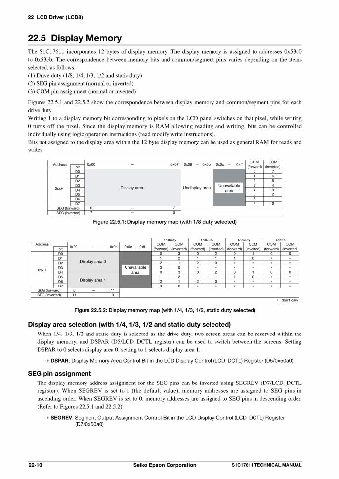
22 LCD Driver (LCD8)
22-10 Seiko Epson Corporation S1C17611 TECHNICAL MANUAL
22.5 Display MemoryThe S1C17611 incorporates 12 bytes of display memory. The display memory is assigned to addresses 0x53c0 to 0x53cb. The correspondence between memory bits and common/segment pins varies depending on the items selected, as follows.(1) Drive duty (1/8, 1/4, 1/3, 1/2 and static duty)(2) SEG pin assignment (normal or inverted)(3) COM pin assignment (normal or inverted)
Figures 22.5.1 and 22.5.2 show the correspondence between display memory and common/segment pins for each drive duty.Writing 1 to a display memory bit corresponding to pixels on the LCD panel switches on that pixel, while writing 0 turns off the pixel. Since the display memory is RAM allowing reading and writing, bits can be controlled individually using logic operation instructions (read modify write instructions).Bits not assigned to the display area within the 12 byte display memory can be used as general RAM for reads and writes.
Display area Undisplay area0xxH
COM(forward)
01234567
COM(inverted)
76543210
bitD0D1D2D3D4D5D6D7
0x00 ··· 0x07 0x08 ··· 0x0b 0x0c ···
07
······
70
SEG (forward)SEG (inverted)
Unavailablearea
Address 0xff
Figure 22.5.1: Display memory map (with 1/8 duty selected)
Display area 0
Display area 1
Address
0xxH
COM(forward)
01230123
COM(inverted)
32103210
1/4DutyCOM
(forward)012∗012∗
COM(inverted)
210∗210∗
1/3DutyCOM
(forward)01∗∗01∗∗
COM(inverted)
10∗∗10∗∗
1/2DutyCOM
(forward)0∗∗∗0∗∗∗
COM(inverted)
0∗∗∗0∗∗∗
Static
0x00 ··· 0x0b 0x0c 0xff···
0 11
······
110
SEG (forward)SEG (inverted)
bitD0D1D2D3D4D5D6D7
∗ : don’t care
Unavailablearea
Figure 22.5.2: Display memory map (with 1/4, 1/3, 1/2, static duty selected)
Display area selection (with 1/4, 1/3, 1/2 and static duty selected) When 1/4, 1/3, 1/2 and static duty is selected as the drive duty, two screen areas can be reserved within the
display memory, and DSPAR (D5/LCD_DCTL register) can be used to switch between the screens. Setting DSPAR to 0 selects display area 0; setting to 1 selects display area 1.
* DSPAR: Display Memory Area Control Bit in the LCD Display Control (LCD_DCTL) Register (D5/0x50a0)
SEG pin assignment The display memory address assignment for the SEG pins can be inverted using SEGREV (D7/LCD_DCTL
register). When SEGREV is set to 1 (the default value), memory addresses are assigned to SEG pins in ascending order. When SEGREV is set to 0, memory addresses are assigned to SEG pins in descending order. (Refer to Figures 22.5.1 and 22.5.2)
* SEGREV: Segment Output Assignment Control Bit in the LCD Display Control (LCD_DCTL) Register (D7/0x50a0)

22 LCD Driver (LCD8)
S1C17611 TECHNICAL MANUAL Seiko Epson Corporation 22-11
COM pin assignment The display memory bit assignment for the COM pins can be inverted using COMREV (D6/LCD_DCTL
register). When COMREV is set to 1 (the default value), memory bits are assigned to COM pins in ascending order. When COMREV is set to 0, memory bits are assigned to COM pins in descending order. (Refer to Figures 22.5.1 and 22.5.2)
* COMREV: Common Output Assignment Control Bit in the LCD Display Control (LCD_DCTL) Register (D6/0x50a0)

22 LCD Driver (LCD8)
22-12 Seiko Epson Corporation S1C17611 TECHNICAL MANUAL
22.6 Display Control
22.6.1 Display On/Off
The LCD display state is controlled using DSPC[1:0] (D[1:0]/LCD_DCTL register).
* DSPC[1:0]: LCD Display Control Bits in the LCD Display Control (LCD_DCTL) Register (D[1:0]/0x50a0)
Table 22.6.1.1: LCD display control
DSPC[1:0] LCD display0x3 All off (static)0x2 All on (dynamic)0x1 Normal display0x0 Display off
(Default: 0x0)
For normal display, set DSPC[1:0] to 0x1. Note that the clock feed must be underway at the time. (See section 22.3.)
If display off is selected, the drive voltage feed from the LCD constant-voltage circuit stops, and pins VC1 to VC3 are all set to VSS level.
Since All on and All off directly control the driving waveform output by the LCD driver, display memory data is not altered. Common pins are set to dynamic drive for All on and to static drive for All off. This function can be used to make the display flash on and off without altering the display memory.
DSPC[1:0] is reset to 0x0 (Display off) after initial resetting or when the slp instruction is executed.
At the time of slp instruction execution, DSPC[1:0] is 0x0 (Display Off) during execution and returns to setting value after returning.
22.6.2 LCD Contrast Adjustment
The LCD contrast can be adjusted to one of 16 gray levels using LC[3:0] (D[3:0]/LCD_CADJ register). Contrast is adjusted by controlling the voltages VC1 to VC3 output by the internal LCD voltage circuit.
* LC[3:0]: LCD Contrast Adjustment Bits in the LCD Contrast Adjust (LCD_CADJ) Register (D[3:0]/0x50a1)
Table 22.6.2.1: LCD contrast adjustment
LC[3:0] Contrast0xf High (dark)0xe ↑
: :0x1 ↓0x0 Low (light)
(Default: 0x0)
LC[3:0] is set to 0x7 after initial resetting. Initialization via software is required to achieve the required contrast.
22.6.3 Inverted Display
The LCD display can be inverted (black/white inversion) using merely control bit manipulation, without changing the display memory. Setting DSPREV (D4/LCD_DCTL register) to 0 inverts the display; setting to 1 returns the display to normal status.
* DSPREV: Reverse Display Control Bit in the LCD Display Control (LCD_DCTL) Register (D4/0x50a0)
Note that the display will not be inverted if All off is selected using DSPC[1:0] (D[1:0]/LCD_DCTL register). The display will be inverted by DSPREV if All on is selected.

22 LCD Driver (LCD8)
S1C17611 TECHNICAL MANUAL Seiko Epson Corporation 22-13
22.7 LCD InterruptThe LCD module includes a function for generating interrupts due to frame signals.
Frame interrupt This interrupt request generated for each frame sets the interrupt flag FRMIF (D0/LCD_IFLG register) to 1
within the LCD module. See Figures 22.4.1 to 22.4.5 for more information on interrupt timing.
* FRMIF: Frame Signal Interrupt Flag in the LCD Interrupt Flag (LCD_IFLG) Register (D0/0x50a6)
To use this interrupt, set FRMIE (D0/LCD_IMSK register) to 1. When FRMIE is set to 0 (the default value), interrupt requests for this interrupt cause are not sent to the interrupt controller (ITC).
* FRMIE: Frame Signal Interrupt Enable Bit in the LCD Interrupt Mask (LCD_IMSK) Register (D0/0x50a5)
If FRMIF is set to 1 while FRMIE is set to 1 (interrupt permitted), the LCD module outputs an interrupt request to the ITC. An interrupt is generated if interrupt conditions are satisfied for the ITC and S1C17 core.
Within the interrupt processing routine, the interrupt cause should be cleared by resetting (writing 1 to) the LCD module FRMIF, rather than using the ITC LCD interrupt flag.
Note: • To prevent interrupt recurrences, the LCD module interrupt flag FRMIF must be reset within the interrupt processing routine following an LCD interrupt.
• To prevent unwanted interrupts, FRMIF should be reset before permitting LCD interrupts with FRMIE.
Interrupt vector The LCD interrupt vector number and vector address are as shown below:
Vector number: 10(0x0a) Vector address: TTBR + 0x28
Other interrupt settings The ITC allows the priority of LCD interrupts to be set between level 0 (the default value) and level 7. To
generate actual interrupts, the PSR (S1C17 core internal processor status register) IE (interrupt enable) bit must be set to 1.
For more information on interrupt processing, see “6 Interrupt Controller (ITC).”

22 LCD Driver (LCD8)
22-14 Seiko Epson Corporation S1C17611 TECHNICAL MANUAL
22.8 Control Register Details
Table 22.8.1: LCD register listAddress Register name Function
0x50a0 LCD_DCTL LCD Display Control Register LCD display control0x50a1 LCD_CADJ LCD Contrast Adjust Register Contrast control0x50a2 LCD_CCTL LCD Clock Control Register LCD clock duty selection
0x50a3 LCD_VREG LCD Voltage Regulator Control Register LCD driver constant-voltage circuit control0x50a5 LCD_IMSK LCD Interrupt Mask Register Interrupt mask setting0x50a6 LCD_IFLG LCD Interrupt Flag Register Interrupt occurrence status display/reset
The individual LCD module registers are described below. These are all 8-bit registers.
Note: When writing data to the registers, always write 0 to bits indicated as “Reserved.” Do not write 1.

22 LCD Driver (LCD8)
S1C17611 TECHNICAL MANUAL Seiko Epson Corporation 22-15
0x50a0: LCD Display Control Register (LCD_DCTL)Register name Address Bit Name Function Setting Init. R/W Remarks
LCD Display Control Register(LCD_DCTL)
0x50a0(8 bits)
D7 SEGREV Segment output assignment control
1 Normal 0 Reverse 1 R/W
D6 COMREV Common output assignment control
1 Normal 0 Reverse 1 R/W
D5 DSPAR Display memory area control 1 Area 1 0 Area 0 0 R/WD4 DSPREV Reverse display control 1 Normal 0 Reverse 1 R/W
D3–2 – reserved – – – 0 when being read.D1–0 DSPC[1:0] LCD display control DSPC[1:0] Display 0x0 R/W
0x30x20x10x0
All offAll on
Normal displayDisplay off
D7 SEGREV: Segment Output Assignment Control Bit Inverts memory assignments for SEG pins. 1 (R/W): Normal (default) 0 (R/W): Inverted
When SEGREV is set to 1 (the default value), memory addresses are assigned to SEG pins in ascending order. When SEGREV is set to 0, memory addresses are assigned to SEG pins in descending order. (Refer to Figures 22.5.1 and 22.5.2)
D6 COMREV: Common Output Assignment Control Bit Inverts memory assignments for COM pins. 1 (R/W): Normal (default) 0 (R/W): Inverted
When COMREV is set to 1 (the default value), memory bits are assigned to COM pins in ascending order. When COMREV is set to 0, memory bits are assigned to COM pins in descending order. (Refer to Figures 22.5.1 and 22.5.2)
D5 DSPAR: Display Memory Area Control Bit Selects the display area when driving using 1/4, 1/3, 1/2 and static duty. 1 (R/W): Display area 1 0 (R/W): Display area 0 (default)
Selects which of the two display areas reserved in the display area is displayed when driving using 1/4, 1/3, 1/2 and static duty. Setting DSPAR to 0 selects display area 0; setting to 1 selects display area 1. Refer to Figure 22.5.2 for more information on display areas.
Display area selection is unavailable for 1/8 duty. Refer to Figure 22.5.1.
D4 DSPREV: Reverse Display Control Bit Inverts (negative display) the LCD display. 1 (R/W): Normal display (default) 0 (R/W): Inverted display
Setting DSPREV to 0 inverts the LCD panel display; setting to 1 returns the display to normal status. This operation does not affect display memory.
D[3:2] Reserved

22 LCD Driver (LCD8)
22-16 Seiko Epson Corporation S1C17611 TECHNICAL MANUAL
D[1:0] DSPC[1:0]: LCD Display Control Bits Control the LCD display.
Table 22.8.2: LCD display control
DSPC[1:0] LCD display0x3 All off (static)0x2 All on (dynamic)0x1 Normal display0x0 Display off
(Default: 0x0)
For normal display, set DSPC[1:0] to 0x1. Note that the clock feed must be underway at the time. (See section 22.3.)
If display off is selected, the drive voltage feed from the LCD constant-voltage circuit stops, and pins VC1 to VC3 are all set to VSS level.
Since All on and All off directly control the driving waveform output by the LCD driver, the display memory data is not altered. Common pins will be set to dynamic drive for All on and to static drive for All off. This function can be used to make the display flash on and off without altering display memory.
DSPC[1:0] is reset to 0x0 (Display off) after initial resetting.
At the time of slp instruction execution, DSPC[1:0] is 0x0 (Display Off) during execution and returns to setting value after returning

22 LCD Driver (LCD8)
S1C17611 TECHNICAL MANUAL Seiko Epson Corporation 22-17
0x50a1: LCD Contrast Adjust Register (LCD_CADJ)Register name Address Bit Name Function Setting Init. R/W Remarks
LCD Contrast Adjust Register(LCD_CADJ)
0x50a1(8 bits)
D7–4 – reserved – – – 0 when being read.D3–0 LC[3:0] LCD contrast adjustment LC[3:0] Display 0x7 R/W
0xf:
0x0
Dark:
Light
D[7:4] Reserved
D[3:0] LC[3:0]: LCD Contrast Adjustment Bits Adjust LCD contrast by controlling voltages VC1 to VC3 output by the internal LCD voltage circuit.
Table 22.8.3: LCD contrast adjustment
LC[3:0] Contrast0xf High (dark)0xe ↑
: :0x1 ↓0x0 Low (light)
(Default: 0x7)
LC[3:0] is set to 0x7 after initial resetting. Initialization via software is required to achieve the required contrast.

22 LCD Driver (LCD8)
22-18 Seiko Epson Corporation S1C17611 TECHNICAL MANUAL
0x50a2: LCD Clock Control Register (LCD_CCTL)Register name Address Bit Name Function Setting Init. R/W Remarks
LCD ClockControl Register(LCD_CCTL)
0x50a2(8 bits)
D7–6 FRMCNT[1:0]
Frame frequency control FRMCNT[1:0] Division ratio 0x1 R/W0x30x20x10x0
LCDclock•1/1024LCDclock•1/680LCDclock•1/512LCDclock•1/256
D5 LFROUT LFR output control 1 On 0 Off 0x0 R/WD4–3 – reserved – – – 0 when being read.D2–0 LDUTY
[2:0]LCD duty select LDUTY[2:0] Duty 0x4 R/W
0x7-0x50x40x30x20x10x0
reserved1/81/41/31/2
Static
D[7:6] FRMCNT [1:0]: Frame Frequency Control Select frame frequency.
Table 22.8.4: Frame frequency when OSC1 (32.768 kHz typ.) is selected as the LCD clock source
Division setting (FRMCNT)
Duty setting (LDUTY)0x0 0x1 0x2 0x3
0x4 (1/8 duty) 128Hz 64Hz 48.19Hz 32Hz0x3 (1/4 duty) 128Hz 64Hz 48.19Hz 32Hz0x2 (1/3 duty) 130.04Hz 65.02Hz 48.12Hz 32.5Hz0x1 (1/2 duty) 128Hz 64Hz 48.19Hz 32Hz0x0 (Static) 128Hz 64Hz 48.19Hz 32Hz
(Default: LDUTY=0x4, FRMCNT=0x1)
Table 22.8.5: Frame frequency when HSCLK is selected as the LCD clock source
Division setting (FRMCNT)
Duty setting (LDUTY)0x0 0x1 0x2 0x3
0x4 (1/8 duty)fhsclk/256 × LCKDV Hz
fhsclk/512 × LCKDV Hz
fhsclk/680 × LCKDV Hz
fhsclk/1024 × LCKDV Hz
0x3 (1/4 duty)fhsclk/256 × LCKDV Hz
fhsclk/512 × LCKDV Hz
fhsclk/680 × LCKDV Hz
fhsclk/1024 × LCKDV Hz
0x2 (1/3 duty)fhsclk/252 × LCKDV Hz
fhsclk/504 × LCKDV Hz
fhsclk/681 × LCKDV Hz
fhsclk/1008 × LCKDV Hz
0x1 (1/2 duty)fhsclk/256 × LCKDV Hz
fhsclk/512 × LCKDV Hz
fhsclk/680 × LCKDV Hz
fhsclk/1024 × LCKDV Hz
0x0 (Static)fhsclk/256 × LCKDV Hz
fhsclk/512 × LCKDV Hz
fhsclk/680 × LCKDV Hz
fhsclk/1024 × LCKDV Hz
(Default: LDUTY=0x4, FRMCNT=0x1)
D5 LFROUT: LFR Output Control Output frame signal. 1 (R/W): Output to P06 0 (R/W): No output
D[4:3] Reserved
D[2:0] LDUTY[2:0]: LCD Duty Select Bits Select the drive duty.
Table 22.8.6: Drive duty settings
LDUTY[2:0] Duty Valid common pin Valid segment pin Max display pixel size0x7–0x5 Reserved – – –
0x4 1/8 COM0 to COM7 SEG0 to SEG15 128 segments0x3 1/4 COM0 to COM3 SEG0 to SEG19 80 segments0x2 1/3 COM0 to COM2 SEG0 to SEG19 60 segments0x1 1/2 COM0 to COM1 SEG0 to SEG19 40 segments0x0 Static COM0 SEG0 to SEG19 20 segments
(Default: 0x4)

22 LCD Driver (LCD8)
S1C17611 TECHNICAL MANUAL Seiko Epson Corporation 22-19
0x50a3: LCD Voltage Regulator Control Register (LCD_VREG)Register name Address Bit Name Function Setting Init. R/W Remarks
LCD Voltage RegulatorControl Register(LCD_VREG)
0x50a3(8 bits)
D7–5 – reserved – – – 0 when being read.D4 LHVLD LCD heavy load protection mode 1 On 0 Off 0 R/W
D3–1 – reserved – – – 0 when being read.D0 VCSEL power source select for LCD
voltage regulator1 VC=2V 0 VC=1V 0 R/W
For more information on these control bits, see “0x50a3: LCD Voltage Regulator Control Register (LCD_VREG)” in section 4.5.

22 LCD Driver (LCD8)
22-20 Seiko Epson Corporation S1C17611 TECHNICAL MANUAL
0x50a5: LCD Interrupt Mask Register (LCD_IMSK)Register name Address Bit Name Function Setting Init. R/W Remarks
LCD Interrupt Mask Register(LCD_IMSK)
0x50a5(8 bits)
D7–1
– reserved – – – 0 when being read.
D0 FRMIE Frame signal interrupt enable 1 Enable 0 Disable 0 R/W
D[7:1] Reserved
D0 FRMIE: Frame Signal Interrupt Enable Bit Permits or prevents frame interrupts. 1 (R/W): Permit interrupt 0 (R/W): Prevent interrupt (default)
Setting FRMIE to 1 permits LCD interrupt requests to the ITC. Setting to 0 prevents interrupts.

22 LCD Driver (LCD8)
S1C17611 TECHNICAL MANUAL Seiko Epson Corporation 22-21
0x50a6: LCD Interrupt Flag Register (LCD_IFLG)Register name Address Bit Name Function Setting Init. R/W Remarks
LCD Interrupt Flag Register(LCD_IFLG)
0x50a6(8 bits)
D7–1
– reserved – – – 0 when being read.
D0 FRMIF Frame signal interrupt flag 1 Occurred 0 Not occurred 0 R/W Reset by writing 1.
D[7:1] Reserved
D0 FRMIF: Frame Signal Interrupt Flag Interrupt flag indicating the frame interrupt cause occurrence status. 1 (R): Interrupt cause present 0 (R): No interrupt cause (default) 1 (W): Reset flag 0 (W): Disable
FRMIF is the LCD module interrupt flag and is set to the frame signal rising edge 1. If FRMIE (D0/LCD_IMSK register) is set to 1 here, an LCD interrupt request signal is output to the ITC. An interrupt is generated if interrupt conditions are satisfied for the ITC and S1C17 core.
FRMIF is reset by writing 1.
Note: • To prevent interrupt recurrences, the LCD module interrupt flag FRMIF must be reset within the interrupt processing routine following an LCD interrupt.
• To prevent unwanted interrupts, FRMIF should be reset before permitting LCD interrupts with FRMIE.
22 LCD Driver (LCD8)
22-22 Seiko Epson Corporation S1C17611 TECHNICAL MANUAL
22.9 Precautions• To prevent interrupt recurrences, the LCD module interrupt flag FRMIF (D0/LCD_IFLG register) must be reset
within the interrupt processing routine following an LCD interrupt.
• To prevent unwanted interrupts, FRMIF (D0/LCD_IFLG register) should be reset before permitting LCD interrupts with FRMIE (D0/LCD_IMSK register).
• See “4.6 Precautions” for LCD power supply precautions.

23 A/D Converter (ADC10SA)
S1C17611 TECHNICAL MANUAL Seiko Epson Corporation 23-1
23 A/D Converter (ADC10SA)
23.1 Outline of A/D ConverterS1C17611 has built-in A/D converter with the following characteristics.
• Conversion method Successive approximation type
• Resolution: 10 bit
• Input channel: Max. 4 channels
• A/D Conversion clock: 2 MHz (Max.)
• Analog input voltage range: VSS–AVDD(=VDD)
• Built-in Sampling & hold circuit
• Converter mode (4 types): 1 time conversion of single channel 1 time conversion of Multi channels Continuous conversion of single channel (end with software control) Continuous conversion of multi channels (end with software control)
• Conversion trigger (3 types): Software trigger External pin (#ADTRG) trigger 16-bit timer Ch.0 underflow trigger
• Conversion result 10 bit can be read by filling to the upper side/lower side.
• Interruption Conversion completion interruption Conversion result overwrite error interruption
Figure 23.1.1 shows structure of A/D converter.
AVDD
AIN3
AIN2
AIN1
AIN0
#ADTRG
+
–
PCLK•1/2 to 1/32768
Bus I/For
Controlregister
Inte
rnal
dat
a b
us
ITC
Timer trigger(16-bit Timer Ch.0)
Sampling and converter with hold circuit
Pre scaller
Successive ApproximationControl circuit
D/Aconverter
Multiplexer
External Trigger
ADCLK
Figure: 23.1.1: A/D Converter Configuration
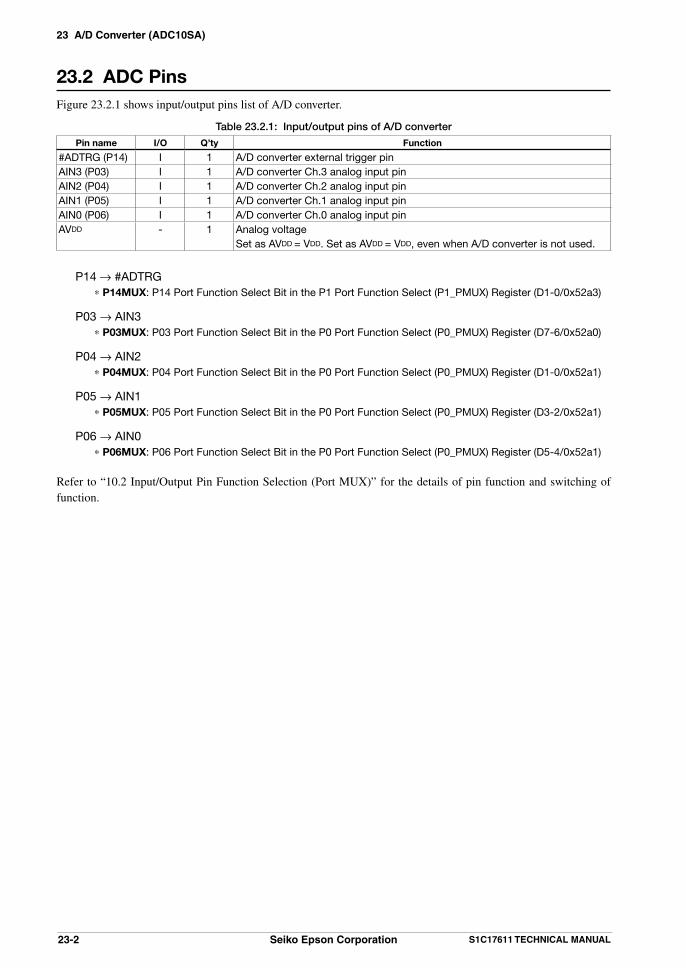
23 A/D Converter (ADC10SA)
23-2 Seiko Epson Corporation S1C17611 TECHNICAL MANUAL
23.2 ADC PinsFigure 23.2.1 shows input/output pins list of A/D converter.
Table 23.2.1: Input/output pins of A/D converter
Pin name I/O Q’ty Function
#ADTRG (P14) I 1 A/D converter external trigger pinAIN3 (P03) I 1 A/D converter Ch.3 analog input pinAIN2 (P04) I 1 A/D converter Ch.2 analog input pinAIN1 (P05) I 1 A/D converter Ch.1 analog input pinAIN0 (P06) I 1 A/D converter Ch.0 analog input pinAVDD - 1 Analog voltage
Set as AVDD = VDD. Set as AVDD = VDD, even when A/D converter is not used.
P14→ #ADTRG* P14MUX: P14 Port Function Select Bit in the P1 Port Function Select (P1_PMUX) Register (D1-0/0x52a3)
P03 → AIN3* P03MUX: P03 Port Function Select Bit in the P0 Port Function Select (P0_PMUX) Register (D7-6/0x52a0)
P04 → AIN2* P04MUX: P04 Port Function Select Bit in the P0 Port Function Select (P0_PMUX) Register (D1-0/0x52a1)
P05 → AIN1* P05MUX: P05 Port Function Select Bit in the P0 Port Function Select (P0_PMUX) Register (D3-2/0x52a1)
P06 → AIN0* P06MUX: P06 Port Function Select Bit in the P0 Port Function Select (P0_PMUX) Register (D5-4/0x52a1)
Refer to “10.2 Input/Output Pin Function Selection (Port MUX)” for the details of pin function and switching of function.

23 A/D Converter (ADC10SA)
S1C17611 TECHNICAL MANUAL Seiko Epson Corporation 23-3
23.3 A/D Converter SettingsTo use the A/D converter, the following settings are required in advance.
1. Setting for analog input pins ... See section 23.22. Setting for A/D conversion clock3. Selection of the start/end channels for analog conversion process4. Setting of A/D conversion mode5. Selection of the trigger type6. Setting of sampling time7. Setting of conversion result storage mode8. Setting for interrupts... See section 23.5
Note: Be sure to disable the A/D converter (set ADEN(D0/ADC10_CTL register)=0) before configuring those settings. Changing settings in enabled state can cause a malfunction.
* ADEN: A/D Enable Bit in the A/D Control/Status (ADC10_CTL) Register (D0/0x5384)
Setting for A/D conversion clock To use the A/D converter, the peripheral clock (PCLK) supplied from the clock generator (CLG) and a
division clock supplied from the Prescaler (PSC) must be turned on. For details, refer to the “8.3 Peripheral Module Clock (PCLK) Control”, and “9.1 Prescaler Configuration.” The A/D converter can select the Prescaler-supplied division clock from 15 types shown in the table
23.3.1.Use ADDF[3:0] (D[3:0]/ADC10_DIV register) for the selection.
* ADDF[3:0]: A/D Converter Clock Divided Frequency Selection Bits in the ADC10 Divided Frequency (ADC10_DIV) Register (D[3:0]/0x5386)
Table 23.3.1: Selection of A/D conversion clock
ADDF[3:0] A/D clock0xf reserved0xe PCLK•1/327680xd PCLK•1/163840xc PCLK•1/81920xb PCLK•1/40960xa PCLK•1/20480x9 PCLK•1/10240x8 PCLK•1/5210x7 PCLK•1/2560x6 PCLK•1/1280x5 PCLK•1/640x4 PCLK•1/320x3 PCLK•1/160x2 PCLK•1/80x1 PCLK•1/40x0 PCLK•1/2
(Default: 0x0)
Note: • For information about restriction of input clock frequencies, refer to “28.7 A/D Converter Characteristics.”
• Do not start A/D conversion while clock output from the Prescaler to the AD converter is turned off, or turn off clock output from the Prescaler while A/D conversion is in process. It can cause a malfunction.
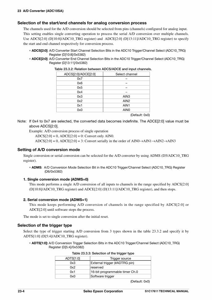
23 A/D Converter (ADC10SA)
23-4 Seiko Epson Corporation S1C17611 TECHNICAL MANUAL
Selection of the start/end channels for analog conversion process The channels used for the A/D conversion should be selected from pins (channels) configured for analog input. This setting enables single converting operation to process the serial A/D conversion over multiple channels.
Use ADCS[2:0] (D[10:8]/ADC10_TRG register) and ADCE[2:0] (D[13:11]/ADC10_TRG register) to specify the start and end channel respectively for conversion process.
* ADCS[2:0]: A/D Converter Start Channel Selection Bits in the ADC10 Trigger/Channel Select (ADC10_TRG) Register (D[10:8]/0x5382)
* ADCE[2:0]: A/D Converter End Channel Selection Bits in the ADC10 Trigger/Channel Select (ADC10_TRG) Register (D[13:11]/0x5382)
Table 23.3.2: Relation between ADCS/ADCE and input channels.
ADCS[2:0]/ADCE[2:0] Select channel0x7 –0x6 –0x5 –0x4 –0x3 AIN30x2 AIN20x1 AIN10x0 AIN0
(Default: 0x0)
Note: If 0x4 to 0x7 are selected, the converted data becomes indefinite. The ADCE[2:0] value must be above ADCS[2:0].
Example: A/D conversion process of single operation ADCS[2:0] = 0, ADCE[2:0] = 0: Convert only AIN0. ADCS[2:0] = 0, ADCE[2:0] = 3: Convert serially in the order of AIN0→AIN1→AIN2→AIN3
Setting of A/D conversion mode Single conversion or serial conversion can be selected for the A/D converter by using ADMS (D5/ADC10_TRG
register).
* ADMS: A/D Conversion Mode Selection Bit in the ADC10 Trigger/Channel Select (ADC10_TRG) Register (D6/0x5382)
1. Single conversion mode (ADMS=0) This mode performs a single A/D conversion of all inputs to channels in the range specified by ADCS[2:0]
(D[10:8]/ADC10_TRG register) and ADCE[2:0] (D[13:11]/ADC10_TRG register), and then stops.
2. Serial conversion mode (ADMS=1) This mode keeps performing A/D conversion of channels in the range specified by ADCS[2:0] or
ADCE[2:0] until software stops the process.
The mode is set to single conversion after the initial reset.
Selection of the trigger type Select the type of trigger starting A/D conversion from 3 types shown in the table 23.3.2 and specify it by
ADTS[1:0] (D[5:4]/ADC10_TRG register).
* ADTS[1:0]: A/D Conversion Trigger Selection Bits in the ADC10 Trigger/Channel Select (ADC10_TRG) Register (D[5:4]/0x5382)
Table 23.3.3: Selection of the trigger type
ADTS[1:0] Trigger source0x3 External trigger (#ADTRG pin)0x2 reserved0x1 16-bit programmable timer Ch.00x0 Software trigger
(Default: 0x0)

23 A/D Converter (ADC10SA)
S1C17611 TECHNICAL MANUAL Seiko Epson Corporation 23-5
1. External trigger (#ADTRG) This type uses an input signal via the #ADTRG pin as a trigger. To use this trigger type, the #ADTRG pin must be configured using the Port Function Select Register. This
type starts A/D conversion by detecting falling edges of #ADTRG signal.
2. 16-bit timer (T16) Ch.0 This type uses an underflow signal of 16-bit timer (T16) Ch.0 as a trigger. The type is effective when
periodic A/D conversion is required because the cycle of the signal can be configured programmably by the timer. For settings for the timer, refer to “11 16-bit Timer (T16).”
3. Software trigger This type uses the software’s writing 1 to ADCTL (D1/AD_CTL register) as a trigger to start A/D
conversion.
* ADCTL: A/D Conversion Control/Status Bit in the ADC10 Control/Status (ADC10_CTL) Register (D1/0x5382)
Setting of sampling time This A/D converter provides ADST[2:0] (D[2:0]/ADC10_TRG register) enabling the input sampling time of
analog signals to be configured to 8 steps (2 to 9 of the conversion clock).
* ADST[2:0]: Sampling Clock Count Bits in the ADC10 Control/Status (AD_CTL) Register (D[2:0]/0x5382)
The sampling time must satisfy the time required for acquiring input voltage (tACQ, acquisition time). Figure 23.3.1 shows the equivalent circuit for the analog input.
Rs: Source impedanceRAIN: Analog input resistanceCAIN: Analog input capacitance
CAINRAINRS
VDD
VSS
Figure 23.3.1: Equivalent circuit for analog input
Configure fADCLK, ADST[2:0] so that tACQ satisfies the following expression. tACQ = 8 × (RS + RAIN) × CAIN (For information of RAIN and CAIN, see “28 Electrical Characteristics.”) 1 × (the number of cycles set by ADST[2:0]) > tACQ fADCLK:A/D conversion clock frequency [Hz] fADCLK
The relationship between the sampling time and the sampling rate is listed below.
fADCLK Sampling rate [sps] = ———————————————————— (Number of clock cycles set by ADST[2:0] + 11)
Setting of conversion result storage mode After completing A/D conversion, this 10-bit A/D converter stores the 10-bit conversion result in the A/D
conversion result storage register ADD[15:0] (D[15:0]/ADC10_ADD register).
* ADD[15:0]: A/D Converted Data Bits in the ADC10 Conversion Result (ADC10_ADD) Register (D[15:0]/0x5380)
The conversion result storage mode can configure STMD (D[7]/ADC10_TRG register), and select either high-order or low-order to store 10-bit A/D conversion result in ADD[15:0].
* STMD: Converted Data Store Mode Bits in the ADC10 Trigger/Channel Select (ADC10_TRG) Register (D[7]/0x5382)

23 A/D Converter (ADC10SA)
23-6 Seiko Epson Corporation S1C17611 TECHNICAL MANUAL
STMD=0: ADD[15:10]=0, ADD[9]= conversion result [MSB], ADD[0]= conversion result [LSB] STMD=1: ADD[15]=[MSB], ADD[6]= conversion result [LSB], ADD[5:0]=0
23.4 A/D Conversion Control and OperationsThe following shows the process of A/D conversion operation
1. Activating A/D converter circuit2. Starting A/D conversion3. Reading A/D conversion result4. Completing A/D conversion
Activating A/D converter circuit After configuring settings shown in the previous section, write 1 to ADEN (D0/ADC10_CTL register) to enable
the A/D converter. This allows the A/D converter to permit a trigger to start A/D conversion. To reconfigure or disable the A/D converter, set the ADEN bit to 0.
* ADEN: A/D Enable Bit in the ADC10 Control/Status (ADC10_CTL) Register (D0/0x5384)
Starting A/D conversion The A/D converter starts A/D conversion if a trigger is input when the ADEN bit is set to 1. When software
trigger is selected, A/D conversion starts by writing 1 to ADCTL (D1/ADC10_CTL register).
* ADCTL: A/D Conversion Control Bit in the ADC10 Control/Status (ADC10_CTL) Register (D1/0x5384)
Triggers other than selected by ADTS[1:0](D[5:4]/ADC10_TRG register) are not permitted.
* ADTS[1:0]: A/D Conversion Trigger Selection Bits in the ADC10 Trigger/Channel Select (ADC10_TRG) Register (D[5:4]/0x5382)
Once a trigger is input, the A/D converter processes the sampling of analog input signals from the conversion starting channel selected by ADCS[2:0] (D[10:8]/ADC10_TRG register) to perform A/D conversion.
* ADCS[2:0]: A/D Converter Start Channel Selection Bits in the ADC10 Trigger/Channel Select (ADC10_TRG) Register (D[10:8]/0x5382)
The ADCTL bit used for software trigger turns to 1 even by the trigger of other type, enabling itself to be used as the status bit for A/D conversion.
ADICH[2:0] (D[2:0]/ADC10_CTL register) can read the channel in conversion process.
* ADICH[2:0]: Internal Conversion Channel Status Bits in the ADC10 Control/Status (ADC10_CTL) Register (D[14:12]/0x5384)
Reading A/D conversion result After completing A/D conversion, the A/D converter stores conversion result in 10-bit data register ADD[15:0]
(D[15:0]/ADC10_ADD register), and set the conversion complete flag ADCF (D8/ADC10_CTL register). If ADCS[2:0] (D[10:8]/ADC10_TRG register) and ADCE[2:0] (D[13:11]/ADC10_TRG register) specify multiple channels, the A/D converter continues A/D conversion for subsequent channels.
* ADD[15:0]: A/D Converted Data Bits in the ADC10 Conversion Result (ADC10_ADD) Register (D[15:0]/0x5380)
* ADCF: Conversion-Complete Flag Bit in the ADC10 Control/Status (ADC10_CTL) Register (D8/0x5384)* ADCE[2:0]: End Channel Selection Bits in the ADC10 Trigger/Channel Select (ADC10_TRG) Register
(D[13:11]/0x5382)
A/D conversion result is stored in ADD[15:0] each time when conversion for a channel is completed. The conversion complete interrupt can be generated concurrently with the storing. The interrupt is usually used to read converted data. If you do not use the conversion complete interrupt, check that the conversion complete factor ADCF (D8/ADC10_CTL register) is set to 1, and then read conversion result from ADD[15:0]. By reading the ADD [15:0] value, the conversion complete interrupt and the ADCF flag are automatically set to 0.

23 A/D Converter (ADC10SA)
S1C17611 TECHNICAL MANUAL Seiko Epson Corporation 23-7
When the serial conversion mode has been selected, conversion result must be read from ADD[15:0] before the next conversion is completed. If you cannot read the conversion result before ADD[15:0] is updated while the conversion complete flag ADCF (D8/ADC10_CTL register) is set to 1, the overwrite error flag ADOWE (D9/ADC10_CTL register) is set to 1, so that you can check that the conversion result has been overwritten. You can also generate the conversion data overwrite interrupt concurrently with overwriting. After reading the conversion result from ADD[15:0], read also the ADOWE flag, or check that the conversion data overwrite interrupt has not occurred so that the read data is valid.
Once the ADOWE flag has been set, it is not reset until software write 1 to the flag. If the ADOWE flag has been reset, the conversion data overwrite interrupt can be stopped to occur.
Note that setting ADOWE flag to 1 also sets the ADCF flag. Therefore, read converted data to reset ADCF to 0.
* ADOWE: Overwrite Error Flag Bit in the ADC10 Control/Status (ADC10_CTL) Register (D9/0x5384)
Note: Occurrence of an overwrite error does not stop serial conversion process.
Completing A/D conversion
• For single conversion mode (ADMS=0) Single conversion mode stops the conversion process once completing a cycle from the start channel specified
by ADCS[2:0] (D[10:8]/ADC10_TRG register) to the end channel ADCE[2:0] (D[13:11]/ADC10_TRG register). After the completion, ADCTL (D1/ADC10_CTL register) is returned to 0.
* ADMS: Conversion Mode Selection bit in the ADC10 Trigger/Channel Select (ADC10_TRG) Register (D6/0x5382)
• For serial conversion mode (ADMS=1) Serial conversion mode maintains the A/D conversion cycles from the start channel to the end channel
continuously. Hardware in this mode does not stop the cycles. Use software to set ADCTL (D1/ADC10_CTL register) to 0 to terminate the process forcibly. And then set ADEN(D0/ADC10_CTL register) to 0. You cannot get data under A/D conversion process when forcible termination occurs.
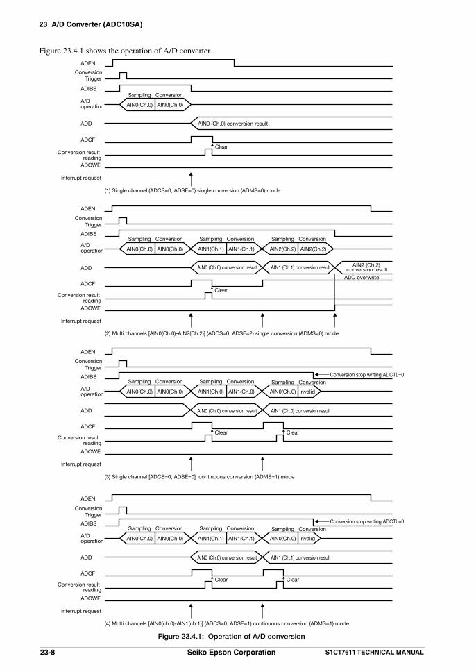
23 A/D Converter (ADC10SA)
23-8 Seiko Epson Corporation S1C17611 TECHNICAL MANUAL
Figure 23.4.1 shows the operation of A/D converter.
ADEN
ADIBSSampling
AIN0(Ch.0) AIN0(Ch.0)
AIN0(Ch.0) AIN0(Ch.0)
AIN0 (Ch.0) conversion result
AIN0 (Ch.0) conversion result AIN1 (Ch.1) conversion result
AIN0 (Ch.0) conversion result AIN1 (Ch.0) conversion result
Conversion stop writing ADCTL=0
AIN2 (Ch.2) conversion result
ADD overwrite
(1) Single channel (ADCS=0, ADSE=0) single conversion (ADMS=0) mode
(2) Multi channels [AIN0(Ch.0)-AIN2(Ch.2)] (ADCS=0, ADSE=2) single conversion (ADMS=0) mode
(3) Single channel [ADCS=0, ADSE=0] continuous conversion (ADMS=1) mode
Conversion
Sampling Conversion
AIN0(Ch.0) AIN0(Ch.0)
Sampling Conversion
AIN1(Ch.1) AIN1(Ch.1)
Sampling Conversion
AIN1(Ch.0) AIN1(Ch.0)
Sampling Conversion
AIN2(Ch.2) AIN2(Ch.2)
Sampling Conversion
AIN0(Ch.0) Invalid
Sampling Conversion
ADIBS
ADIBS
A/D operation
A/D operation
A/D operation
ADD
ADD
ADD
ADCF
ADCF
ADCF
ADOWE
ADOWE
ADOWE
ADEN
ADEN
Conversion result reading
Conversion result reading
Conversion result reading
Interrupt request
Interrupt request
Interrupt request
AIN0 (Ch.0) conversion result AIN1 (Ch.1) conversion result
Conversion stop writing ADCTL=0
(4) Multi channels [AIN0(ch.0)-AIN1(ch.1)] (ADCS=0, ADSE=1) continuous conversion (ADMS=1) mode
AIN0(Ch.0) AIN0(Ch.0)
Clear Clear
Sampling Conversion
AIN1(Ch.1) AIN1(Ch.1)
Sampling Conversion
AIN0(Ch.0) Invalid
Sampling ConversionADIBS
A/D operation
ADD
ADCF
ADOWE
ADEN
ConversionTrigger
ConversionTrigger
ConversionTrigger
ConversionTrigger
Conversion result reading
Interrupt request
Clear Clear
Clear
Clear
Figure 23.4.1: Operation of A/D conversion

23 A/D Converter (ADC10SA)
S1C17611 TECHNICAL MANUAL Seiko Epson Corporation 23-9
23.5 A/D Converter InterruptThe A/D converter provides function of generating the following 2 types of interrupts.• Conversion complete interrupt• Conversion data overwrite interruptThe A/D converter outputs an interrupt signal shared by those 2 types of interrupt factors to the interrupt controller (ITC). To determine the generated interrupt factor, read a relevant interrupt factor register.
Conversion complete interrupt Once completing A/D conversion for a channel, and if ADCIE (D4/ADC10_CTL register) is set to 1 (default:0),
the A/D converter outputs the conversion complete interrupt signal to the controller (ITC) to request an interrupt.
* ADCIE: Conversion-Complete Interrupt Enable Bit in the ADC10 Control/Status (ADC10_CTL) Register (D4/0x5384)
By reading ADD[15:0] (D[15:0]/ADC10_ADD register), the conversion complete interrupt factor is automatically cleared, and ADCF (D8/ADC10_CTL register) is also reset from 1 to 0. To disable generation of the conversion complete interrupt, set the ADCIE bit to 0.
Conversion data overwrite interrupt When the ADD[15:0] register has not been read before it is overwritten by the subsequent A/D conversion
result, and if ADOIE (D5/ADC10_CTL register) is set to 1 (default:0), the A/D converter outputs the conversion data overwrite interrupt signal to the controller (ITC) to request an interrupt.
* ADOIE: Overwrite Interrupt Enable Bit in the ADC10 Control/Status (ADC10_CTL) Register (D5/0x5384)
By writing 1 to ADOWE (D9/ADC10_CTL register), the conversion data overwrite interrupt factor is reset to 0.
* ADOWE: Overwrite Error Flag Bit in the ADC10 Control/Status (ADC10_CTL) Register (D9/0x5384)
To disable generation of the conversion data overwrite interrupt, set the ADOIE bit to 0.
23 A/D Converter (ADC10SA)
23-10 Seiko Epson Corporation S1C17611 TECHNICAL MANUAL
ITC register for A/D converter interrupts Table 23.5.1 shows the ITC control register corresponding to the A/D converter interrupt factors.
Table 23.5.1: ITC register
Interrupt factor interrupt level setting bitConversion complete/Conversion data overwrite ILV18[2:0] (D[2:0]/ITC_LV9)
ITC_LV9 register (0x4318)
Specify the A/D converter interrupt level (0 to 7) for the interrupt level bit. The S1C17 core permits an interrupt when all of the following conditions are met:
• The interrupt enable bit of the A/D converter module is set to 1.• The IE (interrupt enable) bit of the PSR (processor status register inside the S1C17 core) is set to 1.• A/D converter interrupts are set to higher level than the value set in IL (Interrupt Level) of PSR.• NMI or other interrupt factor with higher priority has not occurred.
For details on the interrupt control register and its operation when an interrupt occurs, refer to “6. Interrupt Controller (ITC).”
Interrupt vector The following shows the vector number and address of A/D converter interrupts.
Table 23.5.2: A/D converter interrupt vector
Interrupt factor Vector No. Vector addressConversion complete/Conversion data overwrite 22 (0x16) TTBR + 0x58

23 A/D Converter (ADC10SA)
S1C17611 TECHNICAL MANUAL Seiko Epson Corporation 23-11
23.6 Controlling Register DetailsTable 23.6.1: ADC10SA register list
Address Register name Function
0x5380 ADC10_ADD ADC10 Conversion Rersult Register AD conversion result0x5382 ADC10_TRG ADC10 Trigger/Channel Select Register Setting of conversion trigger/conversion channel0x5384 ADC10_CTL ADC10 Control/Status Register Conversion control, conversion status0x5386 ADC10_DIV ADC10 Divided Frequency Register A/D conversion clock division setting
Each register of ADC10SA module is explained below. These are 16-bit registers.
Note: Write 0 in “Reserved” bit while writing the data to the register. Do not write 1.

23 A/D Converter (ADC10SA)
23-12 Seiko Epson Corporation S1C17611 TECHNICAL MANUAL
0x5380: ADC10 Conversion Result Register (ADC10_ADD)Register name Address Bit Name Function Setting Init. R/W Remarks
A/D Conversion Result Register (ADC10_ADD)
0x5380(16 bits)
D15–0 ADD[15:0] A/D converted data@STMD=0ADD[15:10]=0, ADD9=MSB, ADD0=LSB@STMD=1ADD15=MSB, ADD6=LSB,ADD[5:0]=0
0–1023 0 R
D[15:0] ADD[15:0]: A/D Converted Data Bits A/D conversion result is stored. Storage methods can be changed by settings of STMD register.
STMD=0 ADD[15:10]=0, ADD[9]=MSB, ADD[0]=LSB STMD=1 ADD[15]=MSB, ADD[6]=LSB, ADD[5:0]=0
This register is read only so writing is not possible. Data is 0 at the time of initial setting.

23 A/D Converter (ADC10SA)
S1C17611 TECHNICAL MANUAL Seiko Epson Corporation 23-13
0x5382: ADC10 Trigger/Channel Select Register (ADC10_TRG)Register name Address Bit Name Function Setting Init. R/W Remarks
A/D trigger/ChannelSelect (ADC10_TRG)
0x5382(16 bits)
D15–14 – reserved – – – 0 when being read.D13–11 ADCE[2:0] End channel selection 0x0–0x7 0 R/WD10–8 ADCS[2:0] Start channel selection 0x0–0x7 0 R/W
D7 STMD Covnerted data store mode 1 AD[9:0], 6’b0
0 6’b0, AD[9:0]
0 R/W
D6 ADMS Conversion mode selection 1 continuous 0 single 0 R/WD5–4 ADTS[1:0] Conversion trigger selection ADTS[1:0] trigger 0 R/W
0x30x20x10x0
#ADTRG pinreserved
16bit timersoftware
D3 – reserved – – – 0 when being read.D2–0 ADST[2:0] Sampling clock count ADST[2:0] count clock 0x7 R/W
0x70x60x50x40x30x20x10x0
9clocks8clocks7clocks6clocks5clocks4clocks3clocks2clocks
D[15:14] Reserved
D[13:11] ADCE[2:0]: End Channel Selection Bits Set the conversion end channel within (0–3) channel numbers. Analog input from the channel set by ADCS register up to the channel set by register can be converted
continuously in 1 A/D conversion. When A/D is to be converted only for 1 channel, set the same channel numbers in ADCS register and
ADCE register. ADCE is set to 0 (AIN0) at the time of initial reset.
D[10:8] ADCS[2:0]: Start Channel Selection Bits Set the conversion start channel with channel numbers (0–3). Analog input from the channel set by this register up to the channel set by ADCE register can be
converted continuously in 1 A/D conversion. When A/D is converted for only 1 channel, set the same channel number in ADCS register and ADCE
register. ADCS is set to 0 (AIN0) at the time of initial reset.
D7 STMD: Converted Data Store Mode Bit Select the method to store conversion result to ADD register. For the details, refer to ADD register. STMD is set to 0 (ADD [15:10]=6’b0, ADD[9]=MSB, ADD[0]=LSB) at the time of initial reset.
D6 ADMS: Conversion Mode Selection Bit Select the A/D conversion mode.
1 (R/W) : Continuous conversion mode 0 (R/W) : Single conversion mode
A/D converter is set to continuous mode by writing 1 to ADMS. A/D conversion in the range of channel selected by ADCS and ADCE can be performed continuously till software stops it.
When ADMS is 0, it operates in single conversion mode and A/D conversion for all inputs in the range of channel selected by ADCS and ADCE register is performed once and stopped.
ADMS is set to 0 (single conversion mode) at the time of initial reset.

23 A/D Converter (ADC10SA)
23-14 Seiko Epson Corporation S1C17611 TECHNICAL MANUAL
D[5:4] ADTS [1:0]: Conversion Trigger Selection Bits Select the trigger method by which A/D conversion is started.
Table 23.6.2: Trigger selection
ADTS1 ADTS0 Trigger
1 1 External trigger (# ADTRG)1 0 Reserved0 1 16 bits programmable timer Ch.00 0 Software
When external trigger is used, select the # ADTRG from the port MUX (For the details, refer to I/O port section and port MUX section).
When 16 bits programmable timer ch0 is used, since the underflow signal becomes trigger, set the period and other settings by programmable timer.
ADTS is set to 0 (software trigger) at the time of initial reset.
D3 Reserved
D[2:0] ADST [2:0]: Sampling Clock Count Bits Sets the sampling time of analog input.
Table 23.6.3: Trigger selection
ADST2 ADST1 ADST0 Sampling time
1 1 1 9 clocks1 1 0 8 clocks1 0 1 7 clocks1 0 0 6 clocks0 1 1 5 clocks0 1 0 4 clocks0 0 1 3 clocks0 0 0 2 clocks
Clock number is an input clock number of A/D converter. ADST is set to 111 (9 clocks) at the time of initial reset.

23 A/D Converter (ADC10SA)
S1C17611 TECHNICAL MANUAL Seiko Epson Corporation 23-15
0x5384: ADC10 Control/Status Register (ADC10_CTL)Register name Address Bit Name Function Setting Init. R/W Remarks
A/D Control/Status Register (ADC10_CTL)
0x5384(16 bits)
D15 – reserved – – – 0 when being read.D14–12 ADICH Internal conversion channel status 0x0–0x7 0 R
D11 – reserved – – – 0 when being read.D10 ADIBS Internal busy status 1 busy 0 idle 0 RD9 ADOWE Overwrite error flag 1 Error 0 Normal 0 R/W Reset by writing 1D8 ADCF Conversion-complete flag 1 Completed 0 Not
completed0 R Reset when ADADD
is read.D7–6 – reserved – – 0 when being read.D5 ADOIE Overwrite interrupt enable 1 Enable 0 Disable 0 R/WD4 ADCIE Conversion-complete interrupt
enable1 Enable 0 Disable 0 R/W
D3–2 – reserved – – 0 when being read.D1 ADCTL conversion control 1 Start/Run 0 Stop 0 R/W Stop by writing 0D0 ADEN A/D enable 1 Enable 0 Disable 0 R/W
D15 Reserved
D[14:12] ADICH [2:0]: Internal Conversion Channel Status Bits Shows the channel numbers (0–7) during A/D conversion. When multi channels make A/D conversion, channels currently under conversion can be confirmed by
reading this bit. ADICH is set to 0 (AIN0) at the time of initial reset.
D11 Reserved
D10 ADIBS: Internal Busy status Bits Shows the status of A/D converter.
1 (R/W) : during conversion 0 (R/W) : Conversion complete
1 is output during A/D conversion and 0 is output after A/D conversion completion.
D9 ADOWE: Overwrite Error Flag Bit This is an interruption flag indicating the status of conversion data overwrite cause
1 (R) : With Interruption cause 0 (R) : Without interruption cause (default) 1 (W) : Reset the flag 0 (W) : Disable
When multi channels make A/D conversion, ADOWE set to 1 if conversion result of next channel is written (overwritten) to conversion data register before resetting the conversion end flag ADCF set by conversion of previous channel by reading conversion data. At that time, if the ADOIE (D5/ADC10_CTL register) is set to 1, overwrite interruption request signal related for ITC is output. If interruption conditions of ITC and S1C17 core are valid, interruption will be occurred.
ADOWE is reset by writing 1.
Note: • After generating overwrite interruption, it is necessary to reset the ADOWE in interruption process routine to prevent the regeneration of same interruption.
• Before permitting overwrite interruption by ADOIE, reset the ADOWE to prevent the generation of unnecessary interruption.
D8 ADCF: Conversion Complete Flag Bit It is an interruption flag indicating condition for generating conversion completion cause.
1 (R) : With interruption cause 0 (R) : Without interruption cause (default) 1 (W) : Disable 0 (W) : Disable
After completion of A/D conversion, if the conversion data is stored to ADD(D[15:0]/ADC10_ADD

23 A/D Converter (ADC10SA)
23-16 Seiko Epson Corporation S1C17611 TECHNICAL MANUAL
register) it is set to 1. At that time, if the ADCIE(D4/ADC10_CTL register) is set to 1, conversion completion interruption request signal for ITC is output. If interruption conditions of ITC and S1C17 core are valid, interruption will be occurred.
It is reset to 0 by reading ADD. When multiple channels make A/D conversion, if next A/D conversion is finished in the status where
ADCF is 1 (before reading conversion data), data register overwrites to the new conversion result and overwrite error is generated. Therefore, it is necessary to reset the ADCF by reading the conversion data before completing the next A/D conversion.
D[7:6] Reserved
D5 ADOIE: Overwrite Interrupt Enable Bit Permits or prohibits the generation of overwrite interruption of A/D conversion result for CPU.
1 (R/W) : Interruption permitted 0 (R/W) : Interruption prohibited
In the interruption enable bit that controls the overwrite interruption of A/D conversion result, when ADOIE is set to 1, interruption is permitted and when it sets to 0, interruption is prohibited. ADOIE is set to 0 (Interruption prohibition) at the time of initial reset.
D4 ADCIE: Conversion-complete Interrupt Enable Bit Permits or prohibits the generation of A/D conversion complete interrupt for CPU.
1 (R/W) : Interruption permitted 0 (R/W) : Interruption prohibited
In the interruption enable bit that controls the A/D conversion complete interruption, when ADCIE is set to 1, interruption is permitted and when it sets to 0, interruption is prohibited. ADCIE is set to 0 (Interruption prohibition) at the time of initial reset.
D[3:2] Reserved
D1 ADCTL: Conversion Control Bit Controls the A/D conversion.
1 (R/W) : Software trigger 0 (R/W) : A/D conversion stop
If the A/D conversion is started by software trigger, 1 is written to ADCTL. In case of other trigger methods, ADCTL is set to 1 by hardware.
ADCTL retained to 1 during A/D conversion. At the time of single conversion mode, if the A/D conversion of specified channels is stopped, ADCTL
returns to 0 and A/D conversion circuit is stopped. When A/D conversion of continuous mode is stopped, write 0 to ADCTL.
When ADEN is 0, a trigger is not accepted. ADCTL is set to 0 (A/D conversion stop) at the time of initial reset.
D0 ADEN: A/D Enable Bit Set the A/D converter to enable (conversion possible status).
1 (R/W) : Enable 0 (R/W) : Disable
A/D converter is enabled by writing 1 to ADEN and it is a condition where A/D conversion (trigger can be received) can be started. When ADEN is 0, A/D converter is set to default status and trigger is not received.
Note that A/D conversion continues running when the ADEN is set to 0 during A/D conversion.When A/D conversion is stopped, write 0 to ADCTL.
Furthermore, when the A/D converter of mode and start/complete channels is to be set, it is set after setting ADEN to 0 in order to avoid the error operation.
ADEN is set to 0 (disable) at the time of initial reset.

23 A/D Converter (ADC10SA)
S1C17611 TECHNICAL MANUAL Seiko Epson Corporation 23-17
0x5386: ADC10 Divided Frequency Register (ADC10_DIV)Register name Address Bit Name Function Setting Init. R/W Remarks
A/D DividedFrequencyRegister(ADC_DIV)
0x5386(16 bits)
D15–4 – reserved – – – 0 when being read.D3–0 ADDF[3:0] A/D converter clock divided
frequency selectADDF[3:0] clock 0 R/W
0xf0xe0xd0xc0xb0xa0x90x80x70x60x50x40x30x20x10x0
reservedPCLK•1/32768PCLK•1/16384PCLK•1/8192PCLK•1/4096PCLK•1/2048PCLK•1/1024PCLK•1/512PCLK•1/256PCLK•1/128PCLK•1/64PCLK•1/32PCLK•1/16PCLK•1/8PCLK•1/4PCLK•1/2
D[15:4] Reserved
D[3:0] ADCTL: A/D Converter Clock Divided Frequency Select Bits A/D conversion clock can be selected from 15 types mentioned above.
Note: • Prescaler should be operated is the precondition for the operation of A/D converter. For the details, refer to CLG chapter, PCLK control section, PSC chapter, prescaler structure section.
• For information about restriction of input clock frequencies, refer to “28.7 A/D Converter Characteristics.”
• When the clock output from prescaler to A/D converter is OFF, never start the A/D conversion nor set the clock output of prescaler during A/D conversion operation to OFF. Otherwise it may cause an error.

23 A/D Converter (ADC10SA)
23-18 Seiko Epson Corporation S1C17611 TECHNICAL MANUAL
23.7 Precautions
• When A/D converter like mode or start/complete channel is to be set, A/D converter should be set to disable status (ADEN (D0/ADC10_CTL register) is 0). It may cause an error if enable status is changed.
• For information about restriction of A/D conversion clock frequencies, refer to “28.7 A/D Converter Characteristics.”
• If the clock output from prescaler to A/D converter is OFF, never start the A/D conversion nor set the clock output of prescaler during A/D conversion operation to OFF. Otherwise it may cause an error.
• ADCF (D8/ADC_CTL register) and ADOWE (D9/ADOWE) will not be fixed after initial reset. Reset the program to prevent the generation of unnecessary interruption.
• After interruption, always reset the interrupt factor flag before resetting PSR or executing the reti instruction to prevent the recurrence of interrupts due to the same interrupt factor.
• If the external triggers are used as A/D conversion triggers, ensure to maintain the length more than 2 cycles of S1C17 core operation clock for Low period of input to # ADTRG pin.
• If 0x4 to 0x7 are selected for ADCS (D10-8/ADC10_TRG register) and ADCE (D13-11/ADC10_TRG register), the converted data becomes indefinite.
• The ADCE (D13-11/ADC10_TRG register) value must be above ADCS (D10-8/ADC10_TRG register).

24 RF Converters (RFC)
S1C17611 TECHNICAL MANUAL Seiko Epson Corporation 24-1
24 RF Converters (RFC)
24.1 Overview of R/F ConverterS1C17611 has built-in R/F converter (RFC) which is A/D converter of CR oscillation system.R/F converter easily implements thermo hygrometer by using resistant sensors like thermistor or humidity sensors.The sensor connected to the R/F converter is converted to the frequency (RKCLK) using CR oscillation circuit.This frequency is counted by measurement counter only for the time set in the time base counter operated by internal clock (TCCLK). The counter value of this measurement counter is a value where the sensor is changed digitally. Moreover, besides performing the sensor oscillations which carries out CR oscillations of sensor, highly precise measurement can be realized by performing reference oscillations which carries out CR oscillation of reference elements having less changes due to external factors excluding the error factors such as voltage change and structure variations. The CR oscillator circuit supports AC drive, external clock inputs as well as usual DC drive, allowing it to accommodate various types of sensors.Figure 24.1.1 shows structure of R/F converter.
RFCLKO
HSCLK
OSC1
OSC
SENB
SENA
REF
RF IN
RFC
RFCLK
TCCLK
Division(1/1 to 1/8)
Time BaseCounterTC23-0
to ITC
Inte
rnal
Dat
a B
us
Overflow/Underflow Signals
Overflow Signal
Count Start / Stop Signal
CR OscillationControlCircuit
MeasurementCounterMC23-0
InterruptOscillating
Circuit
CounterControlCircuit
OscillatingCircuit
Gate
Figure 24.1.1: Structure of R/F Converter

24 RF Converters (RFC)
24-2 Seiko Epson Corporation S1C17611 TECHNICAL MANUAL
24.2 RFC pinsTable 24.2.1 shows a list of input/output pins on the R/F converter.
Table 24.2.1 RFC pin list
Pin name I/O Q’ty FunctionSENB (P12)
I/O 1RFC sensor B oscillation control pin. When switching functions, the initial state is HI-Z.
SENA (P11)I/O 1
RFC sensor A oscillation control pin. When switching functions, the initial state is HI-Z.
REF (P10)I/O 1
RFC reference oscillation control pin. When switching functions, the initial state is HI-Z.
RFIN (P07)I/O 1
RFCLK input and oscillation control pin. When switching functions, the initial state is Vss.
RFCLKO (P02) O 1 PFCLK monitoring output pin. RFCLK is output to monitor frequencies.
Note: RFIN is turned to Vss when switching functions. This may cause a high current when RFIN is biased externally.
RFC pins are shared with general purpose input/output pins, and initially set as general purpose input/output pins. To use them as R/F converter pins, the P0_PMUX and P1_PMUX registers must be set to change the function. Set the following control bits to switch the pins function to R/F converter mode.
P12 → SENB* P12MUX: P12 Port Function Select Bit in the P1 Port Function Select (P1_PMUX) Register (D5-4/0x52a2)
P11 → SENA* P11MUX: P11 Port Function Select Bit in the P1 Port Function Select (P1_PMUX) Register (D3-2/0x52a2)
P10 → REF* P10MUX: P10 Port Function Select Bit in the P1 Port Function Select (P1_PMUX) Register (D1-0/0x52a2)
P07 → RFIN* P07MUX: P07 Port Function Select Bit in the P0 Port Function Select (P0_PMUX) Register (D7-6/0x52a1)
P02 → RFCLKO* P02MUX: P02 Port Function Select Bit in the P0 Port Function Select (P0_PMUX) Register (D5-4/0x52a0)
For details on pin function and switching, refer to “10.2 Input/Output Pin Function Selection (Port MUX).”

24 RF Converters (RFC)
S1C17611 TECHNICAL MANUAL Seiko Epson Corporation 24-3
24.3 Operation Mode R/F converter has 3 measurement modes according to self oscillations and mode measuring external clock entry. Moreover, as a function to confirm self oscillation frequency, continuous oscillation function which do not make to strop CR oscillation automatically irrespective of change condition and monitor function of the CR oscillation clock (RFCLK) are provided. These modes can be set per channel.
DC oscillation mode for measuring resistive sensor It is a mode that can observe the difference between reference resistance and oscillation cycles of resistive
sensor, Resistive sensor and reference register are DC driven. 1 reference register and maximum 2 resistive sensors can be connected to 1 channel. When only 1 resistive sensor is in use, unused pin is set to “Open”.
Set SMODE register to “0” to enable this function. Set the function of the required pins to R/F converter for each channel (Refer to the “10.2 Input/Output Pin Function Selection (Port MUX)”). Reference oscillation startup, sensor A oscillation startup and sensor B oscillation startup are set by using SREF register, SSENA register and SSENB register respectively.
RREF: Reference Resistance
RSEN1: Resistive Sensor
RSEN2: Resistive Sensor
CREF: Reference Capacity
Direction of current flow
(DC driven)REF
SENA
SENB
RFINRREF
RSEN1
RSEN2
CREF
Figure 24.3.1: Example of DC Oscillation Mode Connection for Measuring Resistive Sensor
AC oscillation mode for measuring resistive sensor This mode can observe the difference between reference resistance and oscillation cycles of resistive sensor.
Resistive sensor and reference resistance are AC driven. One each of reference register and resistive sensor can be connected.
Set SMODE register to “1” to enable this function. Set the function of the required pins to R/F converter for each channel (Refer to the “10.2 Input/Output Pin Function Selection (Port MUX)”). Reference oscillation startup is set by using SREF register and sensor oscillation startup is set by using SSENA register.
RREF : Reference Resistance
RSEN : Resistive Sensor
CREF : Reference Capacity
RREF
REF
SENA
SENB
RFIN
CREF
RSEN
Direction of current flow (AC driven)
Figure 24.3.2: Example of AC Oscillation Mode Connection for Measuring Resistive Sensor

24 RF Converters (RFC)
24-4 Seiko Epson Corporation S1C17611 TECHNICAL MANUAL
DC oscillation mode for measuring capacitive sensor It is a mode that can observe the difference between the reference capacity and oscillation cycles of capacitive
sensor. Capacitive sensor and reference capacity are DC driven. 1 reference capacity and 1 resistive capacity can be connected. Set SMODE register to “2” to enable this function. Set the function of the required pins to R/F converter for each channel (Refer to the “10.2 Input/Output Pin Function Selection (Port MUX)”). Reference oscillation startup and sensor oscillation startup is set by using SREF register and SSENA register respectively.
RREF: Reference Resistance
CREF: Reference Capacity
CSEN: Capacitive Sensor
REF
SENA
SENB
RFIN
CREF
CSENRREF
Direction of current flow (DC driven)
Figure 24.3.3: Example of DC Oscillation Mode for Measuring Capacitive Sensor Connection
External clock input mode (Event counter mode) It is a mode that can count the pulses from the external oscillation circuit. Not only rectangle wave, but triangle
wave, sign wave can also be entered (For the range of threshould value on schmitt input, refer to “28 Electrical Characteristics” and unused pin is set to “Open”.
EVTEN register is set to “1” to enable this function. Converting operations are executed according to the mode set in SMODE register. Set the function of the required pins to R/F converter for each channel (Refer to the “10.2 Input/Output Pin Function Selection (Port MUX)”).
RFIN
REF
SENA
SENB
Supports Triangle Wave /Rectangular Wave /
Sign Wave
OPEN
OPEN
OPEN
Figure 24.3.4: Example of External Clock Input Mode Connection

24 RF Converters (RFC)
S1C17611 TECHNICAL MANUAL Seiko Epson Corporation 24-5
CR Oscilliation Clock (RFCLK) Monitor Function The CR oscillation clock (RFCLK) under the process of conversion can be output to the pin to monitor. This
function is used to measure self-Oscillating frequency. Set the pin function to RFCLKO by using port MUX register to enable this function. (Refer to “10.2 Input/
Output Pin Function Selection (Port MUX)”.
CR Oscillation Frequency
SSENA, SSENB, SREFRegister
RFIN Pin
RFCLK 0 Pin VSS
VDD
Figure 24.3.5 CR Oscillation Clock (RFCLK) Wave Form
Continous oscillation function CR oscillation of the sensor and the reference resistance will be stopped automatically by stop condition. By using this function, settings can be performed such that CR oscillations will not be stopped irrespective of
stop conditions. This function can easily measure self-oscillating frequency, since it is simultaneously used with the CR oscillation clock monitor function. Set CONEN register to “1” to enable this function.

24 RF Converters (RFC)
24-6 Seiko Epson Corporation S1C17611 TECHNICAL MANUAL
24.4 Conversion OperationsConversion operations of the R/F converter are performed by following sequence of Initial settings → Reference oscillation → Sensor oscillation for irrespective of operation mode. The sequence is shown below.
Initial Settings(1) Select TCCLK frequency which is the counter clock of the time base counter. Refer to “7.9 RFC Clock
Control” (2) Enable TCCLK. Refer to “7.9 RFC Clock Control”. (3) Enable the port to be used by the R/F converter. Refer to “10.2 Input/Output Pin Function Selection (Port
MUX)”. Note: Enable TCCLK and then set the R/F converter. R/F converter does not operate normally, if
TCCLK is not provided
Mode settings of the R/F converter (1) Set RFCEN register =1 and enable R/F converter. (2) Set the conversion mode by using SMODE register.
* RFCEN : RFC Enable Bit in the RFC Control (RFC_CTL) Register (D0/0x53a0) * SMODE : Sensor Oscillation Mode Select in the RFC Control (RFC_CTL) Register (04-5/0x53a0)
Settings and conversion of reference oscillation (1) Set the initial value to MC23-0 register (Measurement Counter). As the measurement counter is up counter,
set complement 2 (0x000000-n) value of the value n to be counted.(2) Initialize the value of TC23-0 register (Time base counter) to 0x000000. (3) Write 1 in OVTCIF and EREFIF register and clear interrupt flag. Note: Oscillation cannot be started if the interrupt flag register is not cleared.(4) Set SREF register to 1 and start the reference oscillation. Note: • First set the value to TC23-0, and wait for the time corresponding to a TCCLK 3 cycle, and
then start oscillation. • For precautions on register settings, refer to details on control registers to prevent
incorrect setting of the value.(5) When the “Measurement counter” or “Time base counter” are overflowed, SREF register turns to 0 and
reference oscillation ends automatically. (6-1) When the measurement counter overflows, EREFIF register is set to 1 with normal exit. Save this Value x
of Time base counter. (6-2) When the time base counter overflows, OVTCIF register set to 1 with error.
* MC23-0 : Measurement Counter Data D23-0 in the RFC Measurement Counter Data (RFC_MC) Register (D23-0/0x53a4/0x53a6)
* TC23-0 : Time Base Counter Data D23-0 in the RFC Time Base Counter Data (RFC_TC) Register (D23-0/0x53a8/0x53aa)
* SREF : Reference Oscillation Start Trigger in the RFC Oscillation Start (RFC_TRG) Register (D0/0x53a2) * OVTCIF : Time Base Counter Over Flow Error Int Enable in the RFC Interrupt Mask (RFC_IMSK) Register
(D4/0x53ac) * EREFIF : Reference Oscillation End Flag in the RFC Interrupt Flag (RFC_IFLG) Register (D0/0x53ae)

24 RF Converters (RFC)
S1C17611 TECHNICAL MANUAL Seiko Epson Corporation 24-7
Measurement CounterMC23-0
Time Base CounterTC23-0
0x00000
0x000000-nInitial Value Settings
Reference Oscillation Start-up
Measurement Counter Overflow(Normal End)
0x000000
x
0x000000-n
Count up
0xFFFFFF
0x00000
Count up
...
Figure 24.4.1 Conversion Operation in Reference Oscillation
Settings and conversion of the sensor oscillation (1) Initialize the MC23-0 register (Measurement counter) value to 0x000000. It is not specifically required to
set, immediately after reference oscillation. (2) Initialize TC23-0 register (Time base counter) value to value x of the time base counter counted in the
reference oscillation. It is not specifically required to set immediately after reference oscillation. (3) Write 1 in OVMCIF, ESENBIF, ESENAIF register and clear interrupt flag. Note: Oscillation cannot be started if the interrupt flag register is not cleared.(4) Set SSENA or SSENB register to 1 and start the sensor oscillation. Note: • First set the value to TC23-0, and wait for the time corresponding to a TCCLK 3 cycle, and
then start oscillation. • For precautions on register settings, refer to details on control registers to prevent
incorrect setting of the value.(5) When the measurement counter overflows or time base counter underflows, SSENA or SSENB register
turns to 0 and sensor oscillation ends automatically. (6-1) When the measurement counter overflows, OVMCIF register set to 1 with error. This measurement
counter value m is processed by the program. (6-2) When the time base counter under flows, ESENAIF or ESENBIF registers are set to 1 with normal end.
* OVMCIF : Measurement Counter Over Flow Error Flag in the RFC Interrupt Flag (RFC_IFLG) Register (D3/0x53ae)
* ESENBIF : Sensor B Oscillation End Flag in the RFC Interrupt Mask (RFC_IFLG) Register (D2/0x53ae) * ESENAIF : Sensor A Oscillation End Flag in the RFC Interrupt Flag (RFC_IFLG) Register (D1/0x53ae)
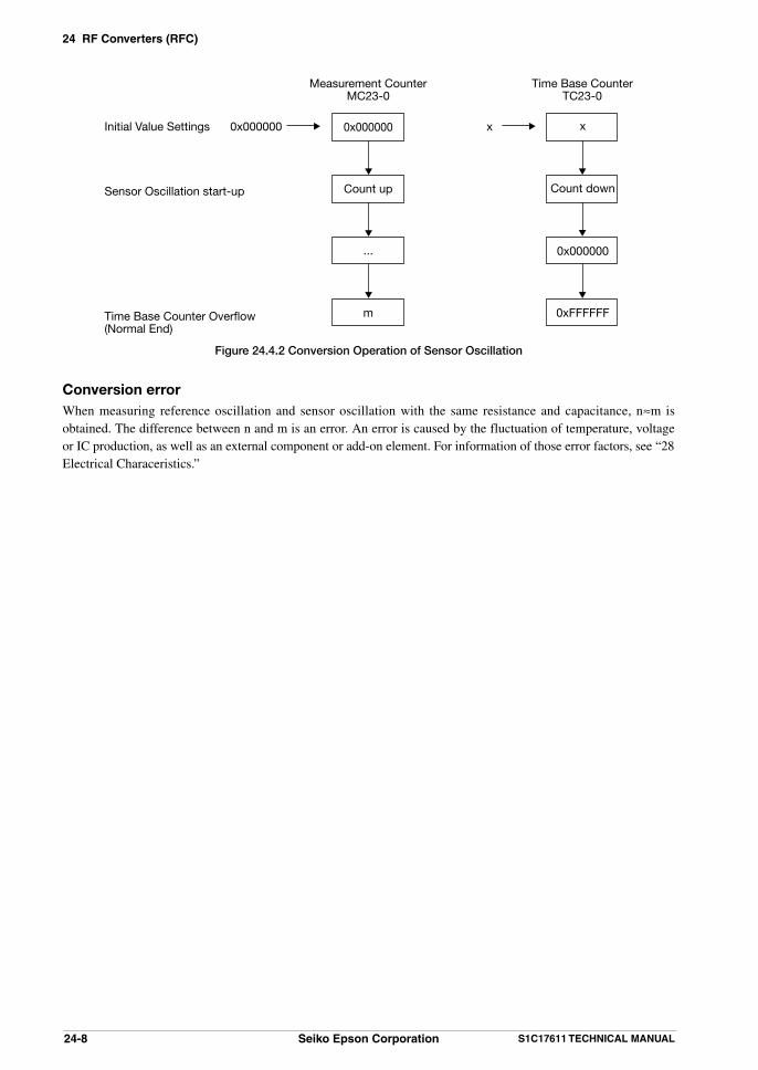
24 RF Converters (RFC)
24-8 Seiko Epson Corporation S1C17611 TECHNICAL MANUAL
Measurement CounterMC23-0
Time Base CounterTC23-0
m
0x000000Initial Value Settings
Sensor Oscillation start-up
Time Base Counter Overflow(Normal End)
x
0xFFFFFF
0x000000
Count up
...
x
Count down
0x000000
Figure 24.4.2 Conversion Operation of Sensor Oscillation
Conversion error When measuring reference oscillation and sensor oscillation with the same resistance and capacitance, n≈m is obtained. The difference between n and m is an error. An error is caused by the fluctuation of temperature, voltage or IC production, as well as an external component or add-on element. For information of those error factors, see “28 Electrical Characeristics.”

24 RF Converters (RFC)
S1C17611 TECHNICAL MANUAL Seiko Epson Corporation 24-9
24.5 R/F Converter Interrupts The R/F converter provides function of generating the following 5 types of interrupts.• Reference oscillation complete interrupt• Sensor A oscillation complete interrupt• Sensor B oscillation complete interrupt• Measurement counter overflow error interrupt• Time base counter overflow error interrupt
The R/F converter outputs an interrupt signal shared by those 5 types of interrupt factors to the interrupt controller (ITC). To determine the generated interrupt factor, read a relevant interrupt factor register.
Reference oscillation complete interruptTo use this interrupt, set EREFIE (D0/RFC_IMSK register) to 1. If the EREFIE bit is set to 0 (default), the interrupt request by this factor is not sent to ITC.
* EREFIE: Reference Oscillation End Int Enable D0 in the RFC Interrupt Enable (RFC_IMSK) Register (D0/0x53ac)
When reference oscillation is completed without an error, that is, when the time base counter does not overflow while the measurement counter overflows and stops, EREFIF (D0/RFC_IFLG register) is set to 1.
* EREFIF: Reference Oscillation End Int Flag D0 in the RFC Interrupt Flag (RFC_IFLG) Register (D0/0x53ae)
Sensor A oscillation complete inerruptTo use this interrupt, set ESENAIE (D1/RFC_IMSK register) to 1. If the ESENAIE bit is set to 0 (default), the interrupt request by this factor is not sent to ITC.
* ESENAIE : Sensor A Oscillation End Int Enable D1 in the RFC Interrupt Enable (RFC_IMSK) Register (D1/0x53ac)
When the sensor A oscillation is completed without an error, that is, when the measurement counter does not overflow while the time base counter overflows and stops, ESENAIF (D1/RFC_IFLG register) is set to 1.
* ESENAIF: Sensor A Oscillation End Int Flag D1 in the RFC Interrupt Flag (RFC_IFLG) Register (D1/0x53ae)
Sensor B oscillation complete inerruptTo use this interrupt, set ESENBIE (D2/RFC_IMSK register) to 1. If the ESENBIE bit is set to 0 (default), the interrupt request by this factor is not sent to ITC.
* ESENBIE: Sensor B Oscillation End Int Enable D2 in the RFC Interrupt Enable (RFC_IMSK) Register (D2/0x53ac)
When the sensor B oscillation is completed without an error, that is, when the measurement counter does not overflow while the time base counter overflows and stops, ESENBIF (D2/RFC_IFLG register) is set to 1.
* ESENBIF: Sensor B Oscillation End Int Flag D2 in the RFC Interrupt Flag (RFC_IFLG) Register (D2/0x53ae)
Measurement counter overflow error interruptTo use this interrupt, set OVMCIE (D3/RFC_IMSK register) to 1. If the OVMCIE bit is set to 0 (default), the interrupt request by this factor is not sent to ITC.
* OVMCIE: Measurement Counter Over Flow Error Interrupt Enable D3 in the RFC Interrupt Enable (RFC_IMSK) Register (D3/0x53ac)
If the measurement counter overflows and stops during sensor oscillation, OVMCIF (D3/RFC_IFLG register) is set to 1 as an error.
* OVMCIF: Measurement Counter Over Flow Error Int Flag D3 in the RFC Interrupt Flag (RFC_IFLG) Register (D3/0x53ae)

24 RF Converters (RFC)
24-10 Seiko Epson Corporation S1C17611 TECHNICAL MANUAL
Time base counter overflow error interruptTo use this interrupt, set OVTCIE (D4/RFC_IMSK register) to 1. If the OVTCIE bit is set to 0 (default), the interrupt request by this factor is not sent to ITC.
* OVTCIE: Time Base Counter Over Flow Error Int Enable D4 in the RFC Interrupt Enable (RFC_IMSK) Register (D4/0x53ac)
If the time base counter overflows and stops during reference oscillation, OVTCIF (D4/RFC_IFLG register) is set to 1 as an error.
* OVTCIF: Time Base Counter Over Flow Error Int Flag D4 in the RFC Interrupt Flag (RFC_IFLG) Register (D4/0x53ae)
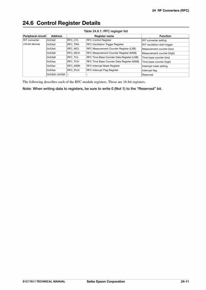
24 RF Converters (RFC)
S1C17611 TECHNICAL MANUAL Seiko Epson Corporation 24-11
24.6 Control Register Details Table 24.6.1: RFC regisger list
Peripheral circuit Address Register name FunctionR/F converter
(16-bit device)
0x53a0 RFC_CTL RFC Control Register R/F converter setting
0x53a2 RFC_TRG RFC Oscillation Trigger Register R/F oscillation start trigger
0x53a4 RFC_MCL RFC Measurement Counter Register (LSB) Measurement counter (low)
0x53a6 RFC_MCH RFC Measurement Counter Register (MSB) Measurement counter (high)
0x53a8 RFC_TCL RFC Time Base Counter Data Register (LSB) Time base counter (low)
0x53aa RFC_TCH RFC Time Base Counter Data Register (MSB) Time base counter (high)
0x53ac RFC_IMSK RFC Interrupt Mask Register Interrupt mask setting
0x53ae RFC_IFLG RFC Interrupt Flag Register Interrupt flag
0x53b0~0x53bf – – Reserved
The following describes each of the RFC module registers. Those are 16-bit registers.
Note: When writing data to registers, be sure to write 0 (Not 1) to the “Reserved” bit.

24 RF Converters (RFC)
24-12 Seiko Epson Corporation S1C17611 TECHNICAL MANUAL
0x53a0: RFC Control Register (RFC_CTL)Register name Address Bit Name Function Setting Init. R/W Remarks
RFC ControlRegister (RFC_CTL)
0x53a0(16 bits)
D15–8 – reserved – – – 0 when being read.D7 CONEN Continuous oscillation enable 1 Enable 0 Disable 0 R/WD6 EVTEN Event counter mode enable 1 Enable 0 Disable 0 R/W
D5–4 SMODE[1:0]
Sensor oscillation mode select0:Resistive sensor DC oscillation1:Resistive sensor AC oscillation2:Capacitive sensor DC oscillation
SMODE[1:0] mode 0 R/W0x30x20x10x0
reservedCDC modeRAC modeRDC mode
D3–1 – reserved – – – 0 when being read.D0 RFCEN RFC Enable 1 Enable 0 Disable 0 R/W
D7 CONEN: Continuous Oscillation Enable Enables continuous oscillation by restricting automatic stop of the CR oscillation.
1 (R/W) : Continuous oscillation enabled 0 (R/W) : Normal (default)
CR oscillation is made not to stop irrespective of stop conditions, if CONEN is set to 1. However, set SREF/SSENA/SSENB register to “Oscillation Start-up” in oscillation start-up.
D6 EVTEN: Event Counter Mode Enable Sets external clock input mode (Event counter mode).
1 (R/W) : External clock input mode 0 (R/W) : Normal (default)
External clock can be entered to the RFIN pin if EVTEN is set to 1. However, to execute conversion operations, it should be set to the “Oscillation start-up” by using SREF/SSENA/SSENB register.
Note: Do not input a clock externally before EVTEN is set to 1. RFIN pin is pull down to VSS at initial status.
D[5:4] SMODE [1:0]: Sensor Oscillation Mode Select Sets Oscillation Mode
0x3 (R/W) : Reserved 0x2 (R/W) : Capacitive Sensor DC Oscillation Mode 0x1 (R/W) : Resistive Sensor AC Oscillation Mode 0x0 (R/W) : Resistive Sensor DC Oscillation Mode (default)
D[3:1] Reserved
D0 RFCEN: RFC Enable Enables/Disables the R/F Converter 1 (R/W) : Enable 0 (R/W) : Disable (default) Conversion operation can be executed if RFCEN is set to 1. When RFCEN is set to 0, operation of
SREF/SSENA/SSENB register is disabled.

24 RF Converters (RFC)
S1C17611 TECHNICAL MANUAL Seiko Epson Corporation 24-13
0x53a2: RFC Oscillation Start Register (RFC_TRG)Register name Address Bit Name Function Setting Init. R/W Remarks
RFC Oscillation trigger (RFC_TRG)
0x53a2(16 bits)
D15–3 – reserved – – – 0 when being read.D2 SSENB Sensor B oscillation Start trigger 1 Read: Run
Write: Start0 Read: Run
Write: Start0 R/W *1*2*3*4
D1 SSENA Sensor A oscillation Start trigger 1 Read: RunWrite: Start
0 Read: RunWrite: Start
0 R/W *1*3*4
D0 SREF Reference dc oscillation Start trigger
1 Read: RunWrite: Start
0 Read: RunWrite: Start
0 R/W *1*3*4
D2 SSENB: Sensor B Oscillation Start Trigger Starts CR oscillation of sensor B.
1 (R) : During oscillation 1 (W) : Oscillation startup 0 (R/W) : Stop (default)
Do not use in resistive sensor AC oscillation mode and capacitive sensor DC oscillation mode.
D1 SSENA: Sensor A Oscillation Start Trigger Starts CR oscillation of sensor A.
1 (R) : During Oscillation 1 (W) : Oscillation start-up 0 (R/W) : Stop (default)
D0 SREF: Reference Oscillation Start Trigger Starts CR oscillation of reference element.
1 (R) : During oscillation 1 (W) : Oscillation startup 0 (R/W) : Stop (default)
Note: *1 Note that, when RFCEN = 0 (Disable), SREF/SSENA/SSENB are disabled. *2 Note that, when SMODE = 1 (RAC MODE), 2 (CDC MODE), writing 1 does not activate
oscillation. *3 Do not set all of the SREF/SSENA/SSENB bits to 1 simultaneously. Be sure to write only to
one bit to start oscillation. *4 Start oscillation after clearing complete flags (EREFIF/ESENAIF/ESENBIF) and overlfow
flags (OVMCIF/OVTCIF).

24 RF Converters (RFC)
24-14 Seiko Epson Corporation S1C17611 TECHNICAL MANUAL
0x53a4/0x53a6: RFC Measurement Counter Data Register (RFC_MC)Register name Address Bit Name Function Setting Init. R/W Remarks
RFC Measurement Counter Data Register (RFC_MC)
0x53a4(16 bits)
D15–0 MC[15:0] Measurement Counter data D15-0 0x0 to 0xffff 0 R/W
0x53a6(16 bits)
D15–8 – reserved – – – 0 when being read.D7–0 MC[23:16] Measurement Counter data
D23-160x0 to 0xff 0 R/W
D[15:0] MC[23:0]: Measurement Counter Data Measurement counter data can be written/read (Default 0x000000).
Note: Set the measurement counter from the lower level value. Upper level value may change due to increase in digit.

24 RF Converters (RFC)
S1C17611 TECHNICAL MANUAL Seiko Epson Corporation 24-15
0x53a8/0x53aa: RFC Time Base Counter Data Register (RFC_TC)Register name Address Bit Name Function Setting Init. R/W Remarks
RFC Time Base Counter Data Register (RFC_TC)
0x53a8(16 bits)
D15–0 TC[15:0] Time base Counter data D15-0 0x0 to 0xffff 0 R/W
0x53aa(16 bits)
D15–8 – reserved – – – 0 when being read.D7–0 TC[23:16] Time base Counter data D23-16 0x0 to 0xff 0 R/W
D[15:0] TC[23:0]: Time Base Counter Data Time base counter data can be written/read (Default 0x000000).
Note: Set the measurement counter from the lower level value. Upper level value may change due to increase in digit.

24 RF Converters (RFC)
24-16 Seiko Epson Corporation S1C17611 TECHNICAL MANUAL
0x53ac: RFC Interrupt Mask Register (RFC_IMSK)Register name Address Bit Name Function Setting Init. R/W Remarks
RFC Interrupt Enable Register (RFC_IMSK)
0x53ac(16 bits)
D15–5 – reserved – – – 0 when being read.D4 OVTCIE Time base Counter Over flow
error interrupt enable1 Enable 0 Disable 0 R/W
D3 OVMCIE Measurement Counter Over flow error interrupt enable
1 Enable 0 Disable 0 R/W
D2 ESENBIE Sensor B oscillation end interrupt Enable
1 Enable 0 Disable 0 R/W
D1 ESENAIE Sensor A oscillation end interrupt Enable
1 Enable 0 Disable 0 R/W
D0 EREFIE Reference oscillation end Interrupt Enable
1 Enable 0 Disable 0 R/W
D4 OVTCIE: Time Base Counter Over Flow Error Interrupt Enable Enables/Disables time base counter over flow error interruption.
1 (R/W) : Enable 0 (R/W) : Disable (default)
D3 OVMCIE: Measurement Counter Over Flow Error Interrupt Enable Enables/Disables measurement counter over flow error interruption
1 (R/W) : Enable 0 (R/W) : Disable (default)
D2 ESENBIE: Sensor B Oscillation End Interrupt Enable Enables/Disables sensor B oscillation end interruption.
1 (R/W) : Enable 0 (R/W) : Disable (default)
D1 ESENAIE: Sensor A Oscillation End Interrupt Enable Enables/Disables sensor A oscillation end interruption.
1 (R/W) : Enable 0 (R/W) : Disable (default)
D0 EREFIE: Reference Oscillation End Interrupt Enable Enables/Disables reference oscillation end interruption.
1 (R/W) : Enable 0 (R/W) : Disable (default)

24 RF Converters (RFC)
S1C17611 TECHNICAL MANUAL Seiko Epson Corporation 24-17
0X53ae: RFC Interrupt Flag Register (RFC_IFLG)Register name Address Bit Name Function Setting Init. R/W Remarks
RFC Interrupt Flag Register (RFC_IFLG)
0x53ae(16 bits)
D15–5 – reserved – – – 0 when being read.D4 OVTCIF Time base Counter Over flow
error interrupt flag1 Cause of
interrupt occurred
0 Cause of interrupt not occurred
0 R/W Reset by writing 1
D3 OVMCIF Measurement Counter Over flow error interrupt flag
1 Cause of interrupt occurred
0 Cause of interrupt not occurred
0 R/W Reset by writing 1
D2 ESENBIF Sensor B oscillation end interrupt flag
1 Cause of interrupt occurred
0 Cause of interrupt not occurred
0 R/W Reset by writing 1
D1 ESENAIF Sensor A oscillation end interrupt flag
1 Cause of interrupt occurred
0 Cause of interrupt not occurred
0 R/W Reset by writing 1
D0 EREFIF Reference oscillation end Interrupt flag
1 Cause of interrupt occurred
0 Cause of interrupt not occurred
0 R/W Reset by writing 1
D4 OVTCIF: Time Base Counter Over Flow Error Flag Time base counter overflow error flag.
1 (R) : Error occurs 1 (W) : Reset to 0 0 (R) : No error (default) 0 (W) : Disable
D3 OVMCIF: Measurement Counter Over Flow Error Flag Measurement counter overflow error flag.
1 (R) : Error occurs 1 (W) : Reset to 0 0 (R) : No error (default) 0 (W) : Disable
D2 ESENBIF: Sensor B Oscillation End Flag Sensor B oscillation end flag.
1 (R) : Oscillation end 1 (W) : Reset to 0 0 (R) : Waiting (default) 0 (W) : Disable
D1 ESENAIF: Sensor A Oscillation End Flag Sensor A oscillation end flag.
1 (R) : Oscillation end 1 (W) : Reset to 0 0 (R) : Waiting (default) 0 (W) : Disable
D0 EREFIF: Reference Oscillation End Flag Reference oscillation end flag.
1 (R) : Oscillation End 1 (W) : Reset to 0 0 (R) : Waiting (default) 0 (W) : Disable

24 RF Converters (RFC)
24-18 Seiko Epson Corporation S1C17611 TECHNICAL MANUAL
24.7 Precautions• Eable TCCLK before configuring R/F converter settings. The R/F converter does not operate normally unless
TCCLK is supplied.• If interrupt flag registers are not cleared, oscillation does not start.• First set the value to TC23-0, and wait for the time corresponding to a TCCLK 3 cycle, and then start oscillation.• For precautions on register settings, refer to details on control registers.
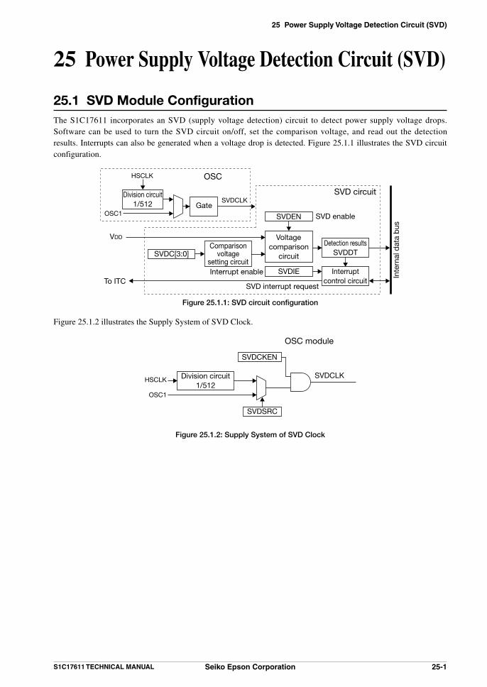
25 Power Supply Voltage Detection Circuit (SVD)
S1C17611 TECHNICAL MANUAL Seiko Epson Corporation 25-1
25 Power Supply Voltage Detection Circuit (SVD)
25.1 SVD Module ConfigurationThe S1C17611 incorporates an SVD (supply voltage detection) circuit to detect power supply voltage drops. Software can be used to turn the SVD circuit on/off, set the comparison voltage, and read out the detection results. Interrupts can also be generated when a voltage drop is detected. Figure 25.1.1 illustrates the SVD circuit configuration.
VDD
Inte
rnal
dat
a b
us
SVD interrupt requestTo ITC
Voltagecomparison
circuit
Interruptcontrol circuit
Comparison voltage
setting circuit
Detection resultsSVDDT
SVD circuit
SVDC[3:0]
Interrupt enable SVDIE
SVD enableSVDEN
OSC
SVDCLK
OSC1
HSCLK
Division circuit1/512 Gate
Figure 25.1.1: SVD circuit configuration
Figure 25.1.2 illustrates the Supply System of SVD Clock.
SVDCLK
OSC1
HSCLK Division circuit1/512
SVDCKEN
SVDSRC
OSC module
Figure 25.1.2: Supply System of SVD Clock

25 Power Supply Voltage Detection Circuit (SVD)
25-2 Seiko Epson Corporation S1C17611 TECHNICAL MANUAL
25.2 SVD ClockOperation clock of SVD (SVDCLK) is generated by SVD clock generator within OSC module. For the details of OSC module refer to “7. Oscillation Circuit (OSC)”.The peripheral module clock (PCLK) is required for writing to registers inside the SVD module, and generation of interrupts. For details, refer to the “8 Clock Generator (CLG)” chapter, and the peripheral module clock (PCLK) section.

25 Power Supply Voltage Detection Circuit (SVD)
S1C17611 TECHNICAL MANUAL Seiko Epson Corporation 25-3
25.3 Comparison Voltage SettingThe SVD circuit compares the power supply voltage (VDD) against the comparison voltage set by the software and outputs results indicating whether the power supply voltage exceeds this comparison voltage. The comparison voltage can be selected from among the 15 listed in Table 25.3.1 with the SVDC[3:0] (D[3:0]/SVD_CMP register).
* SVDC[3:0]: SVD Compare Voltage Select Bits in the SVD Compare Voltage (SVD_CMP) Register (D[3:0]/0x5101)
Table 25.3.1: Comparison voltage settings
SVDC[3:0] Comparison voltage0xf 3.2V0xe 3.1V0xd 3.0V0xc 2.9V0xb 2.8V0xa 2.7V0x9 2.6V0x8 2.5V0x7 2.4V0x6 2.3V0x5 2.2V0x4 2.1V0x3 2.0V0x2 1.9V0x1 1.8V0x0 reserved
(Default: 0x0)

25 Power Supply Voltage Detection Circuit (SVD)
25-4 Seiko Epson Corporation S1C17611 TECHNICAL MANUAL
25.4 SVD Circuit ControlPower supply voltage detection using the SVD circuit is initiated by writing 1 to SVDEN (D0/SVD_EN register) and is stopped by writing 0.
* SVDEN: SVD Enable Bit in the SVD Enable (SVD_EN) Register (D0/0x5100)
The results can be read out from the SVDDT (D0/SVD_RSLT register).
* SVDDT: SVD Detection Result Bit in the SVD Detection Result (SVD_RSLT) Register (D0/0x5102)
The detection results and SVDDT readings are as follows.
• When power supply voltage (VDD) ≥ comparison voltage: SVDDT = 0• When power supply voltage (VDD) < comparison voltage: SVDDT = 1
When SVD interrupts are permitted and SVDEN is set to 1, an interrupt is generated as soon as the power supply voltage drops below the comparison voltage, and the detection result becomes 1. This interrupt can be used to indicate battery depletion and heavy load protection. See the following section for more information on interrupt control.Note that if a temporary voltage drop causes an interrupt, the interrupt will not be canceled even when the voltage subsequently returns to a value exceeding the comparison voltage. The SVDDT should be read and checked in the interrupt processing routine.
Note: • SVD circuit enable response time may be required to obtain stable detection results after the SVDEN (D0/SVD_EN register) changes to set from 0 to 1. SVD circuit response time may be required to obtain stable detection results after the SVDC[3:0](D3-0/SVD_CMP register) changes.
About these response time, see “28.6 SVD Circuit Characteristics.”
• Operating the SVD circuit increases current consumption. If power supply voltage detection is not required, stop SVD operations by setting SVDEN to 0.

25 Power Supply Voltage Detection Circuit (SVD)
S1C17611 TECHNICAL MANUAL Seiko Epson Corporation 25-5
25.5 SVD InterruptThe SVD module includes a function for generating interrupts when power supply voltage drops are detected.
Power supply voltage detection interrupt This interrupt request is generated when the power supply voltage (VDD) detected value drops below the
comparison voltage while SVD is operating (SVDEN (D0/SVD_EN register) = 1). It sets the interrupt flag SVDIF (D0/SVD_IFLG register) to 1 within the SVD module. Once set, SVDIF is not reset even if the power supply voltage subsequently returns to a value exceeding the comparison voltage.
* SVDIF: SVD Interrupt Flag in the SVD Interrupt Flag (SVD_IFLG) Register (D0/0x5104)
To use this interrupt, set SVDIE (D0/SVD_IMSK register) to 1. When SVDIE is set to 0 (the default value), interrupt request for this cause will not be sent to the interrupt controller (ITC).
* SVDIE: SVD Interrupt Enable Bit in the SVD Interrupt Mask (SVD_IMSK) Register (D0/0x5103)
If SVDIF is set to 1 while SVDIE is set to 1 (interrupt permitted), the SVD module outputs an interrupt request to the ITC. An interrupt is generated if interrupt conditions are satisfied for the ITC and S1C17 core.
Note: • To prevent interrupt recurrences, the SVD module interrupt flag SVDIF must be reset within the interrupt processing routine following an SVD interrupt.
• To prevent unwanted interrupts, reset SVDIF before permitting SVD interrupts with SVDIE.
Interrupt vector The SVD interrupt vector number and vector address are as shown below:
Vector number: 9(0x09) Vector address: TTBR + 0x24
Other interrupt settings The ITC allows the priority of SVD interrupts to be set between level 0 (the default value) and level 7. To
generate actual interrupts, the PSR (S1C17 core internal processor status register) IE (interrupt enable) bit must be set to 1.
For more information on interrupt processing, see “6 Interrupt Controller (ITC).”

25 Power Supply Voltage Detection Circuit (SVD)
25-6 Seiko Epson Corporation S1C17611 TECHNICAL MANUAL
25.6 Control Register Details
Table 25.6.1: SVD register listAddress Register name Function
0x5100 SVD_EN SVD Enable Register SVD operation permission0x5101 SVD_CMP SVD Compare Voltage Register Comparison voltage setting0x5102 SVD_RSLT SVD Detection Result Register Voltage detection result
0x5103 SVD_IMSK SVD Interrupt Mask Register Interrupt mask setting0x5104 SVD_IFLG SVD Interrupt Flag Register Interrupt occurrence status display/reset
The individual SVD module registers are described below. These are all 8-bit registers.
Note: When writing data to the registers, always write 0 to bits indicated as “Reserved.” Do not write 1.
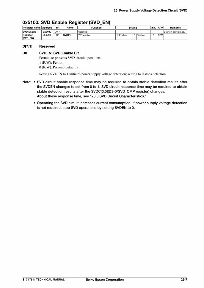
25 Power Supply Voltage Detection Circuit (SVD)
S1C17611 TECHNICAL MANUAL Seiko Epson Corporation 25-7
0x5100: SVD Enable Register (SVD_EN)Register name Address Bit Name Function Setting Init. R/W Remarks
SVD Enable Register(SVD_EN)
0x5100(8 bits)
D7–1 – reserved – – – 0 when being read.D0 SVDEN SVD enable 1 Enable 0 Disable 0 R/W
D[7:1] Reserved
D0 SVDEN: SVD Enable Bit Permits or prevents SVD circuit operations. 1 (R/W): Permit 0 (R/W): Prevent (default )
Setting SVDEN to 1 initiates power supply voltage detection; setting to 0 stops detection.
Note: • SVD circuit enable response time may be required to obtain stable detection results after the SVDEN changes to set from 0 to 1. SVD circuit response time may be required to obtain stable detection results after the SVDC[3:0](D3-0/SVD_CMP register) changes.
About these response time, see “28.6 SVD Circuit Characteristics.”
• Operating the SVD circuit increases current consumption. If power supply voltage detection is not required, stop SVD operations by setting SVDEN to 0.

25 Power Supply Voltage Detection Circuit (SVD)
25-8 Seiko Epson Corporation S1C17611 TECHNICAL MANUAL
0x5101: SVD Compare Voltage Register (SVD_CMP)Register name Address Bit Name Function Setting Init. R/W Remarks
SVD Compare Voltage Register(SVD_CMP)
0x5101(8 bits)
D7–4 – reserved – – – 0 when being read.D3–0 SVDC[3:0] SVD compare voltage SVDC[3:0] Voltage 0x0 R/W
0xf0xe0xd0xc0xb0xa0x90x80x70x60x50x40x30x20x10x0
3.2 V3.1 V3.0 V2.9 V2.8 V2.7 V2.6 V2.5 V2.4 V2.3 V2.2 V2.1 V2.0 V1.9 V1.8 V
reserved
D[7:4] Reserved
D[3:0] SVDC[3:0]: SVD Compare Voltage Select Bits Selects one of 15 comparison voltages for detecting voltage drops.
Table 25.6.2: Comparison voltage settings
SVDC[3:0] Comparison voltage0xf 3.2V0xe 3.1V0xd 3.0V0xc 2.9V0xb 2.8V0xa 2.7V0x9 2.6V0x8 2.5V0x7 2.4V0x6 2.3V0x5 2.2V0x4 2.1V0x3 2.0V0x2 1.9V0x1 1.8V0x0 reserved
(Default: 0x0)
The SVD circuit compares the power supply voltage (VDD) against the comparison voltage set by SVDC[3:0], and outputs results indicating whether the power supply voltage exceeds this comparison voltage.

25 Power Supply Voltage Detection Circuit (SVD)
S1C17611 TECHNICAL MANUAL Seiko Epson Corporation 25-9
0x5102: SVD Detection Result Register (SVD_RSLT)Register name Address Bit Name Function Setting Init. R/W Remarks
SVD Detection Result Register(SVD_RSLT)
0x5102(8 bits)
D7–1 – reserved – – – 0 when being read.D0 SVDDT SVD detection result 1 Low 0 Normal × R
D[7:1] Reserved
D0 SVDDT: SVD Detection Result Bit Reads out power supply voltage detection results. 1 (R): power supply voltage (VDD) < comparison voltage 0 (R): power supply voltage (VDD) ≥ comparison voltage
The SVD circuit compares the power supply voltage (VDD) against the voltage set in SVDC[3:0] (D[3:0]/SVD_CMP register) while SVDEN (D0/SVD_EN register) = 1. The current power supply voltage status can be checked by reading SVDDT.

25 Power Supply Voltage Detection Circuit (SVD)
25-10 Seiko Epson Corporation S1C17611 TECHNICAL MANUAL
0x5103: SVD Interrupt Mask Register (SVD_IMSK)Register name Address Bit Name Function Setting Init. R/W Remarks
SVD Interrupt Mask Register(SVD_IMSK)
0x5103(8 bits)
D7–1 – reserved – – – 0 when being read.D0 SVDIE SVD interrupt enable 1 Enable 0 Disable 0 R/W
D[7:1] Reserved
D0 SVDIE: SVD Interrupt Enable Bit Permits or prevents interrupts when a power supply voltage drop is detected. 1 (R/W): Permit interrupt 0 (R/W): Prevent interrupt (default)
Setting SVDIE to 1 permits SVD interrupt requests to the ITC; setting to 0 prevents interrupts.

25 Power Supply Voltage Detection Circuit (SVD)
S1C17611 TECHNICAL MANUAL Seiko Epson Corporation 25-11
0x5104: SVD Interrupt Flag Register (SVD_IFLG)Register name Address Bit Name Function Setting Init. R/W Remarks
SVD Interrupt Flag Register(SVD_IFLG)
0x5104(8 bits)
D7–1 – reserved – – – 0 when being read.D0 SVDIF SVD interrupt flag 1 Cause of
interrupt occurred
0 Cause of interrupt not occurred
0 R/W Reset by writing 1.
D[7:1] Reserved
D0 SVDIF: SVD Interrupt Flag Interrupt flag indicating the power supply voltage drop detection interrupt cause occurrence status. 1 (R): Interrupt cause present 0 (R): No interrupt cause (default) 1 (W): Reset flag 0 (W): Disable
SVDIF, the SVD module interrupt flag, is set to 1 when a power supply voltage drop is detected. If SVDIE (D0/SVD_IMSK register) is set to 1 here, an SVD interrupt request signal is output to the ITC. An interrupt is generated if interrupt conditions are satisfied for the ITC and S1C17 core.
SVDIF is reset by writing a 1 to it.
Note: • To prevent interrupt recurrences, the SVD module interrupt flag SVDIF must be reset within the interrupt processing routine following an SVD interrupt.
• To prevent unwanted interrupts, reset SVDIF before permitting SVD interrupts with SVDIE (D0/SVD_IMSK register).

25 Power Supply Voltage Detection Circuit (SVD)
25-12 Seiko Epson Corporation S1C17611 TECHNICAL MANUAL
25.7 Precautions• Up to 500 μs may be required to obtain stable detection results after the SVD circuit begins operating. When
reading detection results without using interrupts, allow this stabilization time to elapse before reading SVDDT (D0/SVD_RSLT register) after writing 1 to SVDEN (D0/SVD_EN register).
• Operating the SVD circuit increases current consumption. If power supply voltage detection is not required, stop SVD operations by setting SVDEN (D0/SVD_EN register) to 0.
• To prevent interrupt recurrences, the SVD module interrupt flag SVDIF (D0/SVD_IFLG register) must be reset within the interrupt processing routine following an SVD interrupt.
• To prevent unwanted interrupts, reset SVDIF (D0/SVD_IFLG register) before permitting SVD interrupts with SVDIE (D0/SVD_IMSK register).
• The SVDCLK clock must be supplied for SVD operation. If any of OSC1/OSC3/IOSC, suppliers for SVDCLK, stops necessary oscillation, first activate the oscillation, and allow the oscillation start time and oscillation stabilization time to elapse, and then start the SVD circuit.

26 On-chip Debugger (DBG)
S1C17611 TECHNICAL MANUAL Seiko Epson Corporation 26-1
26 On-chip Debugger (DBG)
26.1 Resource Requirements and Debugging Tool
Debugging work area Debugging requires a 64-byte debugging work area. In the S1C17611, RAM addresses 0x0007c0 to 0x0007ff
are assigned as the debugging work area. When using the debugging function, avoid using this area for any other user applications.
The start address for this debugging work area can be read from the DBRAM register (0xffff90).
Debugging tool Debugging involves connecting an ICD (In-Circuit Debugger) such as S5U1C17001H (ICD Mini) to the
S1C17611 debug pin and inputting the debug instruction from the PC debugger. The following tools are required:
• S1C17 Family In-Circuit Debugger (e.g., S5U1C17001H)• S1C17 Family C compiler package (e.g., S5U1C17001C)
Debug pins The following debug pins are used to connect an ICD (e.g., S5U1C17001H).
Table 26.1.1: Debug pin list
Pin name I/O Qty FunctionDCLK O 1 On-chip debugger clock output pin
Outputs a clock to the ICD Mini (S5U1C17001H).DSIO (P21) I/O 1 On-chip debugger data input/output pin
Used for inputting/outputting debugging data and inputting break signals.DST2 (P22) O 1 On-chip debugger status signal output pin
Outputs the processor status during debugging.
Shared with general purpose input/output port pins (P22, P21), the on-chip debugger input/output pins (DST2, DSIO) are initially set for use as debugger pins. If the debugging function is not used, these pins can be switched via the P2_PMUX register to enable use as general purpose input/output port pins. Set the control bits shown below to 1 to switch the pins to general purpose input/output port use.
DST2 →P22* P22MUX: P22 Port Function Select Bit in the P2 Port Function Select (P2_PMUX) Register (D4/0x52a4)
DSIO → P21* P21MUX: P21 Port Function Select Bit in the P2 Port Function Select (P2_PMUX) Register (D2/0x52a4)
For more information on pin function and switching, refer to “10.2 Input/Output Pin Function Selection (Port MUX).”

26 On-chip Debugger (DBG)
26-2 Seiko Epson Corporation S1C17611 TECHNICAL MANUAL
26.2 Debug Break Operation StatusThe S1C17 core switches to debug mode when the brk instruction is executed or a debug interrupt is generated by a break signal (Low) input to the DSIO pin. This state persists until the retd instruction is executed.During this time, hardware interrupts and NMI are disabled.The default setting halts peripheral circuit operations. This setting can be modified even when debugging is underway.The LCD driver, R/F converter and SVD continue the status where a debug interrupt occurs.
Peripheral circuits that operate using the prescaler output clock• 8-bit timer• 16-bit timer• PWM timer• P port• UART• SPI• I2C (master/slave)• ADC
With the default settings, the prescaler will stop in debug mode, also stopping the peripheral circuits above that use the prescaler output clock. The prescaler includes PRUND (D1/PSC_CTL register) to specify prescaler operations during debug mode. When PRUND is set to 1, the prescaler operates even in debug mode, allowing the peripheral circuits above to operate as well. When PRUND is 0 (default), the prescaler and the peripheral circuits above will stop when the S1C17 core switches to debug mode.
* PRUND: Prescaler Run/Stop Setting (in Debug Mode) Bit in the Prescaler Control (PSC_CTL) Register (D1/0x4020)
Peripheral circuits that operate using the OSC1 clock• Clock timer• Watchdog timer• Stopwatch timer• 8-bit OSC1 timer
The MISC register includes O1DBG (D0/MISC_OSC1 register) to specify the operation of the above OSC1 peripheral circuits during debug mode. When O1DBG is set to 1, the OSC1 peripheral circuits operate even in debug mode. When O1DBG is 0 (default), the OSC1 peripheral circuits will stop when the S1C17 core switches to debug mode.
* O1DBG: OSC1 Peripheral Control (in Debug Mode) Bit in the OSC1 Peripheral Control (MISC_OSC1) Register (D0/0x5322)

26 On-chip Debugger (DBG)
S1C17611 TECHNICAL MANUAL Seiko Epson Corporation 26-3
26.3 Additional Debugging FunctionThe S1C17611 expands the following on-chip debugging functions of the S1C17 core.
Branching destination in debug mode When a debug interrupt is generated, the S1C17 core enters debug mode and branches to the debug processing
routine. In this process, the S1C17 core is designed to branch to address 0xfffc00. In addition to this branching destination, the S1C17611 also allows designation of address 0x0 (beginning address of internal RAM) as the branching destination when debug mode is activated. The branching destination address is selected using DBADR (D8/MISC_IRAMSZ register). When the DBADR is set to "0" (default), the branching destination is set to 0xfffc00. When it is set to "1," the branching destination is set to 0x0.
* DBADR: Debug Base Address Select Bit in the IRAM Size Select (MISC_IRAMSZ) Register (D8/0x5326)
Adding instruction breaks The S1C17 core supports two instruction breaks (hardware PC breaks). The S1C17611 increased this number
to five, adding the control bits and registers given below.
* IBE2: Instruction Break #2 Enable Bit in the Debug Control (DCR) Register (D5/0xffffa0)* IBE3: Instruction Break #3 Enable Bit in the Debug Control (DCR) Register (D6/0xffffa0)* IBE4: Instruction Break #4 Enable Bit in the Debug Control (DCR) Register (D7/0xffffa0)* IBAR2[23:0]: Instruction Break Address #2 Bits in the Instruction Break Address (IBAR2) Register 2
(D[23:0]/0xffffb8)* IBAR3[23:0]: Instruction Break Address #3 Bits in the Instruction Break Address (IBAR3) Register 3
(D[23:0]/0xffffbc)* IBAR4[23:0]: Instruction Break Address #4 Bits in the Instruction Break Address (IBAR4) Register 4
(D[23:0]/0xffffd0)
To use five hardware PC breaks (including four user breaks, and one reserved), the S1C17 Software Integrated Development Environment GNU17 (ver. 1.2.1 or later) must be installed.

26 On-chip Debugger (DBG)
26-4 Seiko Epson Corporation S1C17611 TECHNICAL MANUAL
26.4 Control Register Details
Table 26.4.1: Debug register listAddress Register name Function
0x5322 MISC_OSC1 OSC1 Peripheral Control Register OSC1 operation peripheral function setting for debugging0x5326 MISC_IRAMSZ IRAM Size Select Register IRAM size selection
0xffff90 DBRAM Debug RAM Base Register Debug RAM base address display
0xffffa0 DCR Debug Control Register Debug control
0xffffb8 IBAR2 Instruction Break Address Register 2 Instruction break address #2 setting
0xffffbc IBAR3 Instruction Break Address Register 3 Instruction break address #3 setting
0xffffd0 IBAR4 Instruction Break Address Register 4 Instruction break address #4 setting
The debug registers are described in detail below.
Note: • When data is written to the registers, the “Reserved” bits must always be written as 0 and not 1.
• For debug registers not described here, refer to the S1C17 Core Manual.

26 On-chip Debugger (DBG)
S1C17611 TECHNICAL MANUAL Seiko Epson Corporation 26-5
0x5322: OSC1 Peripheral Control Register (MISC_OSC1) Register name Address Bit Name Function Setting Init. R/W Remarks
OSC1 Peripheral Control Register(MISC_OSC1)
0x5322(16 bits)
D15–1 – reserved – – – 0 when being read.D0 O1DBG OSC1 peripheral control in debug
mode1 Run 0 Stop 0 R/W
D[7:1] Reserved
D0 O1DBG: OSC1 Peripheral Control in Debug Mode Bit Sets OSC1 peripheral circuit operation in debug mode. 1 (R/W): Operate 0 (R/W): Stop (default)
OSC1 peripheral circuit refers to the following peripheral circuits that operate using the OSC1 clock. • Clock timer • Watchdog timer • Stopwatch timer • 8-bit OSC1 timer

26 On-chip Debugger (DBG)
26-6 Seiko Epson Corporation S1C17611 TECHNICAL MANUAL
0x5326: IRAM Size Select Register (MISC_IRAMSZ)Register name Address Bit Name Function Setting Init. R/W Remarks
IRAM Size Select Register(MISC_IRAMSZ)
0x5326(16 bits)
D15–3 – reserved – – – 0 when being read.D8 DBADR Debug base address select 1 0x0 0 0xfffc00 0 R/W
D6–4 IRAMACTSZ[2:0]
IRAM actual size register 0x3 2KB 0x3 R
D2–0 IRAMSZ[2:0] IRAM size select IRAMSZ[2:0] Read cycle 0x3 R/W0x70x60x50x40x30x20x10x0
reservedreserved
512B1KB2KB
reservedreservedreserved
D[15:9] Reserved
D8 DBADR: Debug Base Address Select Bit Selects the address to branch to in the event of a debug interrupt. 1(R/W): 0x0 0(R/W): 0xfffc00 (default)
D7 Reserved
D[6:4] IRAMACTSZ[2:0]: IRAM Actual Size Bits Indicated the mounted internal RAM size.
D3 Reserved
D[2:0] IRAMSZ[2:0]: IRAM Size Select Bits Select the internal RAM size used.
Table 26.4.2: Internal RAM size selection
IRAMSZ[2:0] Internal RAM size0x7 reserved0x6 reserved0x5 512B0x4 1KB0x3 2KB0x2 reserved0x1 reserved0x0 reserved
(Default: 0x3)
Note: The IRAM Size Select Register is write-protected. The write-protection must be overridden by writing 0x96 to the MISC Protect Register (0x5324). Note that MISC Protect Register (0x5324) should normally be set to a value other than 0x96, except when writing to the IRAM Size Select Register. Unnecessary writes may result in system malfunctions.

26 On-chip Debugger (DBG)
S1C17611 TECHNICAL MANUAL Seiko Epson Corporation 26-7
0xffff90: Debug RAM Base Register (DBRAM) Register name Address Bit Name Function Setting Init. R/W Remarks
Debug RAM Base Register(DBRAM)
0xffff90(32 bits)
D31–24 – Unused (fixed at 0) 0x0 0x0 RD23–0 DBRAM[23:0] Debug RAM base address 0x07c0 0x07c0 R
D[31:24] Not used (Fixed at 0)
D[23:0] DBRAM[23:0]: Debug RAM Base Address Bits Read-only register containing the initial address of the debugging work area (64 bytes).

26 On-chip Debugger (DBG)
26-8 Seiko Epson Corporation S1C17611 TECHNICAL MANUAL
0xffffa0: Debug Control Register (DCR)Register name Address Bit Name Function Setting Init. R/W Remarks
Debug ControlRegister(DCR)
0xffffa0(8 bits)
D7 IBE4 Instruction break #4 enable 1 Enable 0 Disable 0 R/WD6 IBE3 Instruction break #3 enable 1 Enable 0 Disable 0 R/WD5 IBE2 Instruction break #2 enable 1 Enable 0 Disable 0 R/WD4 DR Debug request flag 1 Occurred 0 Not occurred 0 R/W Reset by writing 1.D3 IBE1 Instruction break #1 enable 1 Enable 0 Disable 0 R/WD2 IBE0 Instruction break #0 enable 1 Enable 0 Disable 0 R/WD1 SE Single step enable 1 Enable 0 Disable 0 R/WD0 DM Debug mode 1 Debug mode 0 User mode 0 R
D7 IBE4: Instruction Break #4 Enable Bit Permits or prohibits instruction break #4. 1(R/W): Permit 0(R/W): Prohibit (default)
If this bit is set to 1, the instruction fetch address and the value set in the Instruction Break Address Register 4 (0xffffd0) are compared. If they match, an instruction break is generated. If this bit is set to 0, no comparison is performed.
D6 IBE3: Instruction Break #3 Enable Bit Permits or prohibits instruction break #3. 1(R/W): Permit 0(R/W): Prohibit (default)
If this bit is set to 1, the instruction fetch address and the value set in the Instruction Break Address Register 3 (0xffffbc) are compared. If they match, an instruction break is generated. If this bit is set to 0, no comparison is performed.
D5 IBE2: Instruction Break #2 Enable Bit Permits or prohibits instruction break #2. 1(R/W): Permit 0(R/W): Prohibit (default)
If this bit is set to 1, the instruction fetch address and the value set in the Instruction Break Address Register 2 (0xffffb8) are compared. If they match, an instruction break is generated. If this bit is set to 0, no comparison is performed.
D4 DR: Debug Request Flag Indicates the presence or absence of an external debug request. 1(R): Request generated 0(R): None (default) 1(W): Resets flag 0(W): Invalid
This flag is cleared (reset to 0) when 1 is written. It must be cleared before the debug processing routine is terminated by the retd instruction.
D3 IBE1: Instruction Break #1 Enable Bit Permits or prohibits instruction break #1. 1(R/W): Permit 0(R/W): Prohibit (default)
If this bit is set to 1, the instruction fetch address and the value set in the Instruction Break Address Register 1 (0xffffb4) are compared. If they match, an instruction break is generated. If this bit is set to 0, no comparison is performed.

26 On-chip Debugger (DBG)
S1C17611 TECHNICAL MANUAL Seiko Epson Corporation 26-9
D2 IBE0: Instruction Break #0 Enable Bit Permits or prohibits instruction break #0. 1(R/W): Permit 0(R/W): Prohibit (default)
If this bit is set to 1, the instruction fetch address and the value set in the Instruction Break Address Register 0 (0xffffb0) are compared. If they match, an instruction break is generated. If this bit is set to 0, no comparison is performed.
D1 SE: Single Step Enable Bit Permits or prohibits single-step operations. 1(R/W): Permit 0(R/W): Prohibit (default)
D0 DM: Debug Mode Bit Indicates the processor operating mode (debug mode or user mode). 1(R): Debug mode 0(R): User mode (default)
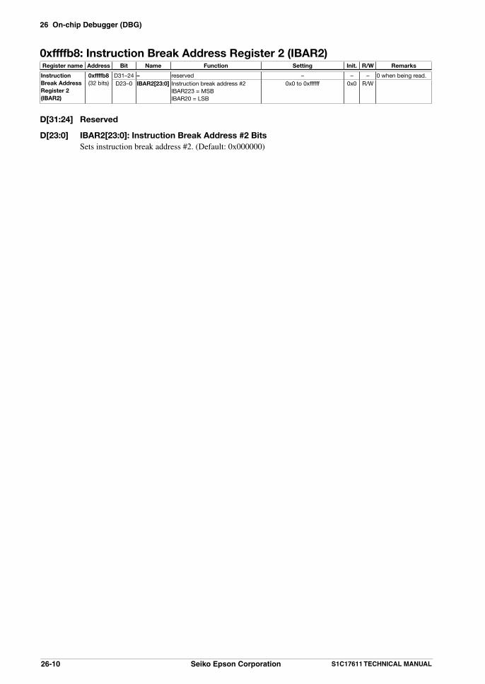
26 On-chip Debugger (DBG)
26-10 Seiko Epson Corporation S1C17611 TECHNICAL MANUAL
0xffffb8: Instruction Break Address Register 2 (IBAR2)Register name Address Bit Name Function Setting Init. R/W Remarks
InstructionBreak AddressRegister 2(IBAR2)
0xffffb8(32 bits)
D31–24 – reserved – – – 0 when being read.D23–0 IBAR2[23:0] Instruction break address #2
IBAR223 = MSBIBAR20 = LSB
0x0 to 0xffffff 0x0 R/W
D[31:24] Reserved
D[23:0] IBAR2[23:0]: Instruction Break Address #2 Bits Sets instruction break address #2. (Default: 0x000000)

26 On-chip Debugger (DBG)
S1C17611 TECHNICAL MANUAL Seiko Epson Corporation 26-11
0xffffbc: Instruction Break Address Register 3 (IBAR3)Register name Address Bit Name Function Setting Init. R/W Remarks
InstructionBreak AddressRegister 3(IBAR3)
0xffffbc(32 bits)
D31–24 – reserved – – – 0 when being read.D23–0 IBAR3[23:0] Instruction break address #3
IBAR323 = MSBIBAR30 = LSB
0x0 to 0xffffff 0x0 R/W
D[31:24] Reserved
D[23:0] IBAR3[23:0]: Instruction Break Address #3 Bits Sets instruction break address #3. (Default: 0x000000)

26 On-chip Debugger (DBG)
26-12 Seiko Epson Corporation S1C17611 TECHNICAL MANUAL
0xffffd0: Instruction Break Address Register 4 (IBAR4)Register name Address Bit Name Function Setting Init. R/W Remarks
InstructionBreak AddressRegister 4(IBAR4)
0xffffd0(32 bits)
D31–24 – reserved – – – 0 when being read.D23–0 IBAR4[23:0] Instruction break address #4
IBAR423 = MSBIBAR40 = LSB
0x0 to 0xffffff 0x0 R/W
D[31:24] Reserved
D[23:0] IBAR4[23:0]: Instruction Break Address #4 Bits Sets instruction break address #4. (Default: 0x000000)

27 Multiplier/Divider
S1C17611 TECHNICAL MANUAL Seiko Epson Corporation 27-1
27 Multiplier/Divider
27.1 OverviewThe S1C17611 incorporates a coprocessor that provides signed/unsigned 16 x 16 bit multiplication functions, 16 ÷ 16 bit division functions, and signed 16 x 16 bit + 32 bit Product-sum calculation (MAC, Multiplyord Accumulator) functions enabling overflow detection.Use of these functions is discussed below.
S1C17 core
Arithmetic unit
Arithmetic result register
Mode setting
Selector
Argument 2
Argument 1
Coprocessoroutput
Flag output
Arithmeticresult
Figure 27.1.1: Multiplier/divider block diagram
Table 27.1.1: Arithmetic cycles
Operation CyclesMultiplication 1 cycle
Product-sum calculation 1 cycleDivision 17 to 20 cycles

27 Multiplier/Divider
27-2 Seiko Epson Corporation S1C17611 TECHNICAL MANUAL
27.2 Operating Mode and Output ModeThe multiplier/divider operates in accordance with the operating mode specified by the application program. The multiplier/divider supports nine different operations, as shown in Table 27.2.1.The multiplication, division, and MAC arithmetic results are 32-bit data. This means the S1C17 core cannot read out results in a single access cycle. The output mode is provided to specify whether the first 16 bits or last 16 bits of the multiplier/divider arithmetic results are read out.Specify the operating and output modes by writing 7-bit data to the multiplier/divider internal mode setting register. Use the “ld.cw” instruction for writing.
ld.cw %rd,%rs %rs[6:0] is written to the mode setting register. (%rd: not used) ld.cw %rd,imm7 imm7[6:0] is written to the mode setting register. (%rd: not used)
6 4 3 0Output mode setting Operating mode setting
Figure 27.2.1: Mode setting registers
Table 27.2.1: Mode setting
Setting (D[6:4])
Output modeSetting (D[3:0])
Operating mode
0x0 Last 16-bit output modeLast 16 bits of the arithmetic results are read out as coprocessor output.
0x0 Initialization mode 0Clears the arithmetic results register to 0x0.
0x1 First 16-bit output modeFirst 16 bits of the arithmetic results are read out as coprocessor output.
0x1 Initialization mode 1Loads the 16-bit arithmetic augend into the last 16 bits of the arithmetic results register.
0x2 to 0x7 Reserved 0x2 Initialization mode 2Loads the 32-bit arithmetic augend into the arithmetic results register.
0x3 Arithmetic results reading modeOutputs the arithmetic results register data without performing calculations.
0x4 Unsigned multiplication modePerforms unsigned multiplication.
0x5 Signed multiplication modePerforms signed multiplication.
0x6 Reserved0x7 Signed MAC mode
Performs signed MAC multiplication.0x8 Unsigned division mode
Performs unsigned division.0x9 Signed division mode
Performs signed division.0xa to 0xf Reserved

27 Multiplier/Divider
S1C17611 TECHNICAL MANUAL Seiko Epson Corporation 27-3
27.3 MultiplicationThe multiplication function executes “A (32 bits) = B (16 bits) x C (16 bits).”To perform multiplication, set the operating mode to 0x4 (unsigned multiplication) or 0x5 (signed multiplication). Next, transfer the 16-bit multiplicand (B) and 16-bit multiplier (C) to the multiplier/divider using the “ld.ca” instruction. Half of the arithmetic result (16 bits, A [15:0] or A[31:16], depending on output mode) is returned to the CPU register, together with the flag status.The remaining half of the arithmetic result is read out by setting the multiplier/divider to arithmetic result reading mode.
S1C17 coreArithmetic result
register
Selector
16 bits
32 bits
Coprocessoroutput (16 bits)
Flag output
Argument 2
Argument 1
Arithmeticresult
Figure 27.3.1: Multiplier mode data paths
Table 27.3.1: Multiplier mode operations
Modesetting
Instruction Operation Flag Remarks
0x04 or
0x05
ld.ca %rd,%rs res[31:0] ← %rd × %rs%rd ← res[15:0]
psr (CVZN) ← 0b0000 The arithmetic result register retains arithmetic results until the results are overwritten by another operation.
(ext imm9) ld.ca %rd,imm7
res[31:0] ← %rd × imm7/16%rd ← res[15:0]
0x14 or
0x15
ld.ca %rd,%rs res[31:0] ← %rd × %rs %rd ← res[31:16]
(ext imm9) ld.ca %rd,imm7
res[31:0] ← %rd × imm7/16 %rd ← res[31:16]
res: Arithmetic result register
Examples:ld.cw %r0,0x4 ; Mode setting (unsigned multiplication mode & last 16-bit output mode)ld.ca %r0,%r1 ; Executes “res = %r0 x %r1” and loads the last 16 bits of the result to %r0 register.ld.cw %r0,0x13 ; Mode setting (arithmetic result reading mode & first 16-bit output mode)ld.ca %r1,%r0 ; Loads the first 16 bits of the result to %r1 register.

27 Multiplier/Divider
27-4 Seiko Epson Corporation S1C17611 TECHNICAL MANUAL
27.4 DivisionThe division function executes "A (16 bits) = B (16 bits) ÷ C (16 bits), D (16 bits) = Remainder."To perform a division, set the operating mode to 0x8 (unsigned division) or 0x9 (signed division). Next, transfer the 16-bit dividend (B) and 16-bit divisor (C) to the multiplier/divider using the “1d.ca” instruction. The quotient will be placed in the lower 16 bits of the arithmetic result register, while the remainder is placed in the upper 16 bits. When the calculation is completed, the 16 bits corresponding to the quotient or remainder as specified in the output mode and the flag status are returned to the CPU register. The other 16 bits of the arithmetic result can be read out by setting the multiplier/divider to arithmetic result reading mode.
S1C17 coreArithmetic result
register
Selector
Argument 2
Argument 1 16 bits
÷
16 bits
Coprocessoroutput (16 bits)
Flag output
Arithmeticresult
Figure 27.4.1 Division mode data path
Table 27.4.1 Division mode operations
Modesetting
Instruction Operation Flag Remarks
0x08 or
0x09
ld.ca %rd,%rs res[31:0] ← %rd ÷ %rs%rd ← res[15:0] (quotient)
psr (CVZN) ← 0b0000 The arithmetic result register re-tains the calculated result until it is overwritten by the result of another arithmetic operation.
(ext imm9) ld.ca %rd,imm7
res[31:0] ← %rd ÷ imm7/16%rd ← res[15:0] (quotient)
0x18 or
0x19
ld.ca %rd,%rs res[31:0] ← %rd ÷ %rs %rd ← res[31:16] (remainder)
(ext imm9) ld.ca %rd,imm7
res[31:0] ← %rd ÷ imm7/16%rd ← res[31:16] (remainder)
res: Arithmetic result register
Example:ld.cw %r0,0x8 ; Mode setting (unsigned division mode & lower 16-bit output mode)ld.ca %r0,%r1 ; Executes “res = %r0 + %r1” and loads the lower 16 bits (quotient) of the result to the
%r0 register.ld.cw %r0,0x13 ; Mode setting (arithmetic result reading mode & upper 16-bit output mode)ld.ca %r1,%r0 ; Loads the upper 16 bits (remainder) of the result to the %r1 register.

27 Multiplier/Divider
S1C17611 TECHNICAL MANUAL Seiko Epson Corporation 27-5
27.5 Product-sum OperationThe Product-sum operation function executes “A (32 bits) = B (16 bits) x C (16 bits) + A (32 bits).”The initial value (A) must be set to the arithmetic result register before performing Product-sum operations.To clear the arithmetic result register (A = 0), set the operating mode to 0x0. There is no need to send 0x0 to the multiplier/divider using separate instructions.To load 16-bit or 32-bit values to the arithmetic result register, set the operating mode to 0x1 (16 bits) or 0x2 (32 bits). Next, transfer the initial value to the multiplier/divider using the “ld.cf” instruction.
S1C17 coreArithmetic result
register
Selector
16 bits
32 bits
Coprocessoroutput (16 bits)
Flag output
Argument 2
Argument 1
Figure 27.5.1: Initialization mode data paths
Table 27.5.1: Arithmetic result register initialization
Modesetting
Instruction Operation Remarks
0x0 – res[31:0] ← 0x0 Initializes using operating mode settings only (no data transfer).
0x1 ld.cf %rd,%rs res[31:16] ← 0x0 res[15:0] ← %rs
(ext imm9) ld.cf %rd,imm7
res[31:16] ← 0x0 res[15:0] ← imm7/16
0x2 ld.cf %rd,%rs res[31:16] ← %rd res[15:0] ← %rs
(ext imm9) ld.cf %rd,imm7
res[31:16] ← %rd res[15:0] ← imm7/16
res: Arithmetic result register
To perform MAC operations, set the operating mode to 0x7 (signed MAC). Next, transfer the 16-bit multiplicand (B) and 16-bit multiplier (C) to the multiplier/divider using the “ld.ca” instruction. Half of the arithmetic result (16 bits, A [15:0] or A[31:16], depending on output mode) is returned to the CPU register together with the flag status. The remaining half of the arithmetic result is read out by setting the multiplier/divider to arithmetic result reading mode.The PSR overflow flag (V) is set to 1 by the arithmetic results. Other flags are cleared to 0.Transfer the required number of multiplicands and multipliers to continue MAC operations without switching to arithmetic result reading mode. In this case, there is no need to set to MAC mode each time data is sent.

27 Multiplier/Divider
27-6 Seiko Epson Corporation S1C17611 TECHNICAL MANUAL
S1C17 coreArithmetic result
register
SelectorCoprocessoroutput (16 bits)
Flag output
16 bits
32 bits
32 bits
Argument 2
Argument 1
Arithmeticresult
Figure 27.5.2: MAC mode data paths
Table 27.5.2: MAC mode operations
Modesetting
Instruction Operation Flag Remarks
0x07 ld.ca %rd,%rs res[31:0] ← %rd × %rs + res[31:0]%rd ← res[15:0]
If overflow occurspsr (CVZN) ← 0b0100
Other casespsr (CVZN) ← 0b0000
The arithmetic result register retains arithmetic results until the results are overwritten by another operation.
(ext imm9) ld.ca %rd,imm7
res[31:0]←%rd × imm7/16 + res[31:0]%rd ← res[15:0]
0x17 ld.ca %rd,%rs res[31:0] ← %rd × %rs + res[31:0]%rd ← res[31:16]
(ext imm9) ld.ca %rd,imm7
res[31:0]←%rd × imm7/16 + res[31:0]%rd ← res[31:16]
res: Arithmetic result register
Examples:ld.cw %r0,0x7 ; Mode setting (signed MAC mode & last 16-bit output mode)ld.ca %r0,%r1 ; Executes “res = %r0 x %r1 + res” and loads the last 16 bits of the result to %r0 register.ld.cw %r0,0x13 ; Mode setting (arithmetic result reading mode & first 16-bit output mode)ld.ca %r1,%r0 ; Loads first 16 bits of the result to %r1 register.
Overflow flag (V) setting conditions If the multiplication result sign, arithmetic result register sign, and arithmetic result sign satisfy the following
conditions in MAC operations, an overflow occurs, and the overflow flag (V) is set to 1.
Table 27.5.3: Overflow flag (V) setting conditions
Mode setting Multiplication result sign Arithmetic result register sign Arithmetic result sign0x07 0 (Positive) 0 (Positive) 1 (Negative)0x07 1 (Negative) 1 (Negative) 0 (Positive)
An overflow occurs if positive values are summed giving a negative result in MAC operations or if negative values are summed giving a positive result. The result is retained in the coprocessor until the overflow flag (V) is cleared.
Overflow flag (V) clear conditions The overflow flag (V) set is cleared if the “ld.ca” instruction is executed for MAC operation without causing
an overflow or if the “ld.ca” or “ld.cf” instruction is executed in other than arithmetic result reading mode.
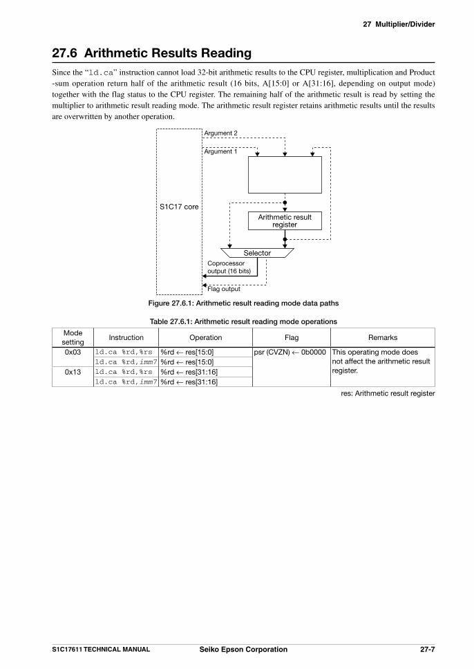
27 Multiplier/Divider
S1C17611 TECHNICAL MANUAL Seiko Epson Corporation 27-7
27.6 Arithmetic Results ReadingSince the “ld.ca” instruction cannot load 32-bit arithmetic results to the CPU register, multiplication and Product -sum operation return half of the arithmetic result (16 bits, A[15:0] or A[31:16], depending on output mode) together with the flag status to the CPU register. The remaining half of the arithmetic result is read by setting the multiplier to arithmetic result reading mode. The arithmetic result register retains arithmetic results until the results are overwritten by another operation.
S1C17 coreArithmetic result
register
SelectorCoprocessoroutput (16 bits)
Flag output
Argument 2
Argument 1
Figure 27.6.1: Arithmetic result reading mode data paths
Table 27.6.1: Arithmetic result reading mode operations
Modesetting
Instruction Operation Flag Remarks
0x03 ld.ca %rd,%rs %rd ← res[15:0] psr (CVZN) ← 0b0000 This operating mode does not affect the arithmetic result register.
ld.ca %rd,imm7 %rd ← res[15:0]0x13 ld.ca %rd,%rs %rd ← res[31:16]
ld.ca %rd,imm7 %rd ← res[31:16]
res: Arithmetic result register

28 Electrical Characteristics
S1C17611 TECHNICAL MANUAL Seiko Epson Corporation 28-1
28 Electrical Characteristics
28.1 Absolute Maximum Ratings(VSS = 0V)
Item Code Condition Rating UnitsPower supply voltage VDD -0.3 to 4.0 VAnalog power supply voltage AVDD VDD=AVDD -0.3 to 4.0 VLCD power supply voltage VC3 -0.3 to 4.0 VInput voltage VI -0.3 to VDD + 0.3 VOutput voltage VO -0.3 to VDD + 0.3 VHigh-level output current IOH 1 pin -5 mA
Total for all pins -20 mALow-level output current IOL 1 pin 5 mA
Total for all pins 20 mAPermissible losses*1 VO 200 mWOperating temperature Ta -25 to 70 °CStorage temperature Tstg -65 to 150 °CSoldering temperature/time Tsol 260°C, 10 s (leads) –*1: For plastic package
28.2 Recommended Operating Conditions
Item Code Condition Min. Typ. Max. UnitsOperating power supply voltage
VDD Normal operating mode 1.8 3.6 VFlash memory programming mode 2.7 3.6 V
Analog operating power supply voltage
AVDD VDD=AVDD 1.8 3.6 V
Operating frequency fOSC3 Crystal/ceramic oscillation 0.2 8.2 MHzfOSC1 Crystal oscillation 32.768 100 kHz
Capacitor between VSS and VD1*1 C1 0.1 µFCapacitor between VSS and VC1*1 C2 0.1 µFCapacitor between VSS and VC2*1 C3 0.1 µFCapacitor between VSS and VC3*1 C4 0.1 µFCapacitor between CA and CB*1 C5 0.1 µF*1: No capacitors are required if no LCD driver is used. VC1 to VC3 and CA to CB should be left open.

28 Electrical Characteristics
28-2 Seiko Epson Corporation S1C17611 TECHNICAL MANUAL
28.3 Current ConsumptionUnless otherwise stated: VDD = 1.8 to 3.6V, VSS = 0V, Ta = 25°C, C1 to C5 = 0.1µF, no load on LCD panel,
PCKEN = 0x3 (ON), VD1MD = 0x0, FLCYC[2:0] = 0x4 (1 cycle), CCKGR[1:0] = 0x0 (gear ratio : 1/1)
Item Code Condition Min. Typ. Max. UnitsSLEEP current consumption
ISLP OSC1=OFF, OSC3=OFF 0.6 3.0 µA
HALT current consumption
IHALT1 OSC1=32kHz, IOSC=OFF, OSC3=OFF, PCKEN=0x0 (OFF)
2.0 4.0 µA
OSC1=32kHz, IOSC=OFF, OSC3=OFF 3.0 6.0 µAIHALT2 OSC1=32kHz, IOSC=OFF,
OSC3=8MHz(ceramic)450 650 µA
IHALT3 OSC1=32kHz, IOSC=ON, OSC3=OFF 170 250 µAExecution current *1
consumptionIEXE1 OSC1=32kHz, IOSC=OFF, OSC3=OFF,
CPU=OSC112 20 µA
OSC1=32kHz, IOSC=OFF, OSC3=OFF, CCKGR=0x2(gear ratio : 1/4), CPU=OSC1
6 10 µA
IEXE2 OSC1=32kHz, IOSC=OFF, OSC3=1MHz(ceramic), CPU=OSC3
400 550 µA
OSC1=32kHz, IOSC=OFF, OSC3=8MHz(ceramic), CPU=OSC3
2500 3500 µA
OSC1=32kHz, IOSC=OFF, OSC3=8MHz(ceramic), CCKGR=0x2(gear ratio : 1/4), CPU=OSC3
1100 1500 µA
IEXE3 OSC1=32kHz, IOSC=ON, OSC3=OFF, CPU=IOSC
850 1200 µA
IEXE11 OSC1=32kHz, IOSC=OFF, OSC3=OFF, VD1MD=0x1, CPU=OSC1
27 38 µA
IEXE21 OSC1=32kHz, IOSC=OFF, OSC3=1MHz (ceramic), VD1MD=0x1, CPU=OSC3
750 1200 µA
OSC1=32kHz, IOSC=OFF, OSC3=8MHz (ceramic), VD1MD=0x1, CPU=OSC3
4200 6200 µA
IEXE31 OSC1=32kHz, IOSC=ON, OSC3=OFF,VD1MD=0x1, CPU=IOSC
1600 2300 µA
IEXE1H OSC1=32kHz, IOSC=OFF, OSC3=OFF,CPU=OSC1, HVLD=0x1
19 30 µA
*1: Execution current consumption is the value for continuous operations while fetching the test program (ALU instruction 60.5%, branch instruction 17%, memory read 12%, memory write 10.5%) from flash memory.
Current consumption and temperature characteristics in Halt mode (OSC1 operation)
OSC1= 32.768 kHz, IOSC = OFF, OSC3 = OFF, PCKEN=0x0 (OFF), CCKGR = 0, Typ. value
Operating current consumption and temperature characteristics (OSC1 operation)
OSC1= 32.768 kHz, IOSC = OFF, OSC3 = OFF, PCKEN=0x3 (ON), CCKGR = 0, Typ. value
5
6
2
1
3
4
0-50 -25 0 25 50 75 100
Ta[°C]
IHA
LT1[
µA]
15
20
25
30
35
VD1MD=1
VD1MD=0
IEX
E1/
IEX
E11
[µA
]
0
5
10
-50 -25 0 25 50 75 100Ta [°C]
Figure 28.3.1 Figure 28.3.2

28 Electrical Characteristics
S1C17611 TECHNICAL MANUAL Seiko Epson Corporation 28-3
Operating current consumption and temperature vs. clock gear characteristics (OSC1 operation)
OSC1= 32.768 kHz, IOSC = OFF, OSC3 = OFF, PCKEN=0x3 (ON), Typ. value
Operating current consumption and frequency characteristics (OSC3 operation)
OSC1 = OFF, IOSC = OFF, PCKEN=0x3 (ON), CCKGR = 0,Ta = 25°C, Typ. value
10
12
14
16
0
2
4
6
8
-50 -25 0 25 50 75 100Ta[°C]
IEX
E1[
µA]
Gear ratio:1/1
Gear ratio:1/2
Gear ratio:1/4Gear ratio:1/8
4000
5000
0
1000
2000
3000
0.0 1.0 2.0 3.0 4.0 5.0 6.0 7.0 8.0 9.0 10.0fosc3[MHz]
IEX
E2/
IEX
E21
[µA
]
VD1MD=1
VD1MD=0
Figure 28.3.3 Figure 28.3.4
Operating current consumption and frequency vs. clock gear characteristics (OSC3 operation)
OSC1 = OFF, IOSC = OFF, PCKEN=0x3 (ON), Ta = 25°C, Typ. value
Operating current consumption and temperature vs. clock gear characteristics (IOSC operation)
OSC1 = OFF, OSC3 = OFF, PCKEN=0x3 (ON), Typ. value
1500
2000
2500
3000
0
500
1000
0.0 1.0 2.0 3.0 4.0 5.0 6.0 7.0 8.0 9.0 10.0fosc3[MHz]
IEX
E2[
µA]
Gear ratio:1/1
Gear ratio:1/2
Gear ratio:1/4Gear ratio:1/8
600
700
800
900
0
200
100
300
400
500
-50 -25 0 25 50 75 100Ta[°C]
IEX
E3[
µA]
Gear ratio:1/2
Gear ratio:1/4Gear ratio:1/8
Gear ratio:1/1
Figure 28.3.5 Figure 28.3.6
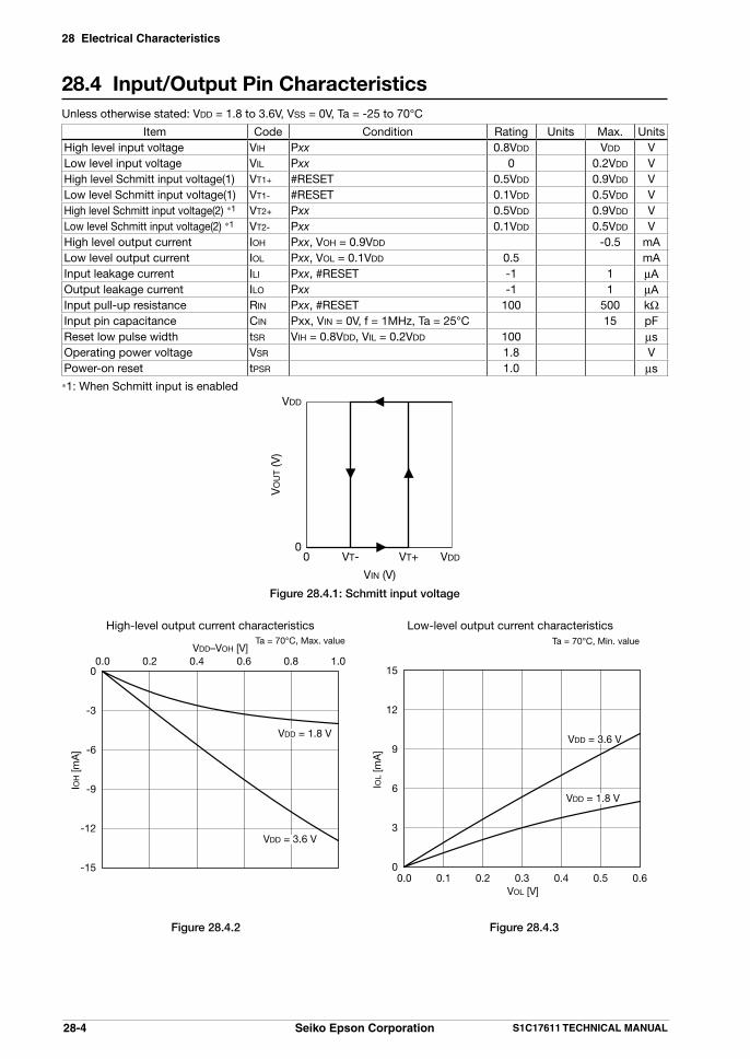
28 Electrical Characteristics
28-4 Seiko Epson Corporation S1C17611 TECHNICAL MANUAL
28.4 Input/Output Pin CharacteristicsUnless otherwise stated: VDD = 1.8 to 3.6V, VSS = 0V, Ta = -25 to 70°C
Item Code Condition Rating Units Max. UnitsHigh level input voltage VIH Pxx 0.8VDD VDD VLow level input voltage VIL Pxx 0 0.2VDD VHigh level Schmitt input voltage(1) VT1+ #RESET 0.5VDD 0.9VDD VLow level Schmitt input voltage(1) VT1- #RESET 0.1VDD 0.5VDD VHigh level Schmitt input voltage(2) *1 VT2+ Pxx 0.5VDD 0.9VDD VLow level Schmitt input voltage(2) *1 VT2- Pxx 0.1VDD 0.5VDD VHigh level output current IOH Pxx, VOH = 0.9VDD -0.5 mALow level output current IOL Pxx, VOL = 0.1VDD 0.5 mAInput leakage current ILI Pxx, #RESET -1 1 µAOutput leakage current ILO Pxx -1 1 µAInput pull-up resistance RIN Pxx, #RESET 100 500 kWInput pin capacitance CIN Pxx, VIN = 0V, f = 1MHz, Ta = 25°C 15 pFReset low pulse width tSR VIH = 0.8VDD, VIL = 0.2VDD 100 µsOperating power voltage VSR 1.8 VPower-on reset tPSR 1.0 µs
*1: When Schmitt input is enabledVDD
0VT+VT-0
VIN (V)
VO
UT
(V)
VDD
Figure 28.4.1: Schmitt input voltage
High-level output current characteristics Low-level output current characteristics
0.00
-3
-6
-9
-12
-15
0.2 0.4 0.6 0.8 1.0VDD–VOH [V]
IOH [m
A]
VDD = 1.8 V
VDD = 3.6 V
Ta = 70°C, Max. value
0.0
15
12
9
6
3
00.1 0.2 0.3 0.4 0.5 0.6
VOL [V]
IOL
[mA
]
VDD = 3.6 V
VDD = 1.8 V
Ta = 70°C, Min. value
Figure 28.4.2 Figure 28.4.3

28 Electrical Characteristics
S1C17611 TECHNICAL MANUAL Seiko Epson Corporation 28-5
#RESET
tSR
VIH
VIL
Figure 28.4.4: Reset timing
VDD
Power supplyturn on
VSSCRES
Vsr
tpsr
0.5VDD
0.1VDD
RESETRESET
Figure 28.4.5: Power-on reset timing Figure 28.4.6: Example of power-on reset circuit

28 Electrical Characteristics
28-6 Seiko Epson Corporation S1C17611 TECHNICAL MANUAL
28.5 LCD Driver Circuit Characteristics
LCD driver voltage characteristicsSince Typ values for the LCD driver will vary depending on panel load (e.g., panel size, drive duty, display pixel illumination number, display patterns), they should be evaluated by connecting the actual panel to be used.
Unless otherwise stated: VDD = 2.5 V to 3.6 V, VSS = 0 V, Ta = 25°C, C1 to C5 = 0.1 µF, When outputting a checkered pattern without panel load. VCSEL register = 0x1 (VC2 standard).
Item Code Condition Min. Typ. Max. UnitsLCD drive voltage(When VC2 stand-ard is selected)
VC1 1 MW load resistor connected between VSS and VC1
0.324•VC3 (typ) 0.350•VC3 (typ) V
VC2 1 MW load resistor connected between VSS and VC2
0.649•VC3 (typ) 0.701•VC3 (typ) V
VC3 1 MW load resis-tor connected between VSS and VC3
LC[3:0] = 0x0
Typ×0.96
2.56
Typ×1.04
VLC[3:0] = 0x1 2.62 VLC[3:0] = 0x2 2.68 VLC[3:0] = 0x3 2.74 VLC[3:0] = 0x4 2.80 VLC[3:0] = 0x5 2.86 VLC[3:0] = 0x6 2.92 VLC[3:0] = 0x7 2.98 VLC[3:0] = 0x8 3.04 VLC[3:0] = 0x9 3.10 VLC[3:0] = 0xa 3.15 VLC[3:0] = 0xb 3.22 VLC[3:0] = 0xc 3.27 VLC[3:0] = 0xd 3.33 VLC[3:0] = 0xe 3.39 VLC[3:0] = 0xf 3.45 V
Unless otherwise stated: VDD = 1.8 V to 3.6 V, VSS = 0 V, Ta = 25°C, C1 to C5 = 0.1 µF, When outputting a checkered pattern without panel load. VCSEL register = 0x0 (VC1 standard).
Item Code Condition Min. Typ. Max. UnitsLCD drive voltage(When VC1 stand-ard is selected)
VC1 1 MW load resistor connected between VSS and VC1
0.333•VC3 (typ) 0.360•VC3 (typ) V
VC2 1 MW load resistor connected between VSS and VC2
0.645•VC3 (typ) 0.696•VC3 (typ) V
VC3 1 MW load resis-tor connected between VSS and VC3
LC[3:0] = 0x0
Typ×0.96
2.50
Typ×1.04
VLC[3:0] = 0x1 2.56 VLC[3:0] = 0x2 2.61 VLC[3:0] = 0x3 2.67 VLC[3:0] = 0x4 2.73 VLC[3:0] = 0x5 2.79 VLC[3:0] = 0x6 2.85 VLC[3:0] = 0x7 2.90 VLC[3:0] = 0x8 2.96 VLC[3:0] = 0x9 3.02 VLC[3:0] = 0xa 3.08 VLC[3:0] = 0xb 3.14 VLC[3:0] = 0xc 3.19 VLC[3:0] = 0xd 3.25 VLC[3:0] = 0xe 3.31 VLC[3:0] = 0xf 3.37 V

28 Electrical Characteristics
S1C17611 TECHNICAL MANUAL Seiko Epson Corporation 28-7
LCD drive voltage and power supply voltage characteristics (while VC2 standard is selected)
When 1 MW load resistance is installed between VSS and VC3.
(No panel load), Ta = 25°C, Typ. value
LCD drive voltage and power supply voltage characteristics (while VC1 standard is selected)
When 1 MW load resistance is installed between VSS and VC3.
(No panel load), Ta = 25°C, Typ.values
3.0
4.0
2.0
VC
3 [V
]
1.0
VDD [V]1.5 2.0 2.5 3.0 3.5 4.0
LCx=0xf
LCx=0x0
3.0
4.0
2.0
1.0
VC
3 [V
]
VDD [V]1.5 2.0 2.5 3.0 3.5 4.0
LCx=0xf
LCx=0x0
Figure 28.5.1 Figure 28.5.2
LCD drive voltage and temperature characteristics
Typ. value (VC2 and VC1 standards)
LCD drive voltage and load characteristics
When load resistance is installed only on the VC3 pin.
LCx = 0xf, Ta = 25°C, Typ. value
1.05VC3
1.04VC3
1.03VC3
1.02VC3
1.01VC3
0.98VC3
0.97VC3
0.96VC3
0.95VC3
099VC3VC
3 [V
]
-50 -25 0 25 50 75 100Ta [°C]
1.00VC3
3.30
3.40
3.50
3.60
2.90
3.00
3.10
3.20 VC
3 [V
]
0 4 8 12 16 20-Ivc3 [µA]
VCSEL=1
VCSEL=0
Figure 28.5.3 Figure 28.5.4
SEG/COM I/O characteristicsUnless otherwise stated: VDD = 1.8 to 3.6V, VSS = 0V, Ta = -25 to 70°C
Item Code Condition Min Typ Max. UnitsSegment, common output current ISEGH SEGxx, COMxx, VSEGH = VC3 - 0.1V -5 µA
ISEGL SEGxx, COMxx, VSEGL = 0.1V 5 µA

28 Electrical Characteristics
28-8 Seiko Epson Corporation S1C17611 TECHNICAL MANUAL
LCD driver circuit current consumptionUnless otherwise stated: VDD = 1.8 V to 3.6 V, VSS = 0 V, Ta = 25°C, C1 to C5 = 0.1 µF, No panel load, PCKEN = 0 (OFF),
FLCYC = 4 (1 cycle), CCLKGR = 0 (gear ratio : 1/1).
Item Code Condition Min. Typ. Max. UnitsVC2 standardLCD circuit current*1
ILCD2 DSPC[1:0]=1(Checker pattern),LC[3:0]=0xf,OSC1=32kHz,VDD=2.5 to 3.6V, VCSEL=1
1 3 µA
Heavy load protection modeVC2 standardLCD circuit current*1
ILCD2H DSPC[1:0]=1(Checker pattern),LC[3:0]=0xf,OSC1=32kHz, VDD=2.5 to 3.6V, LHVLD=1VCSEL=1
21 32 µA
VC1 standardLCD circuit current*1
ILCD1 DSPC[1:0]=1(Checker pattern), LC[3:0]=0xf,OSC1=32kHz,VDD=1.8 to 3.6V, VCSEL=0
1.5 5 µA
Heavy load protection modeVC1 standardLCD circuit current*1
ILCD1H DSPC[1:0]=1(Checker pattern), LC[3:0]=0xf,OSC1=32kHz, VDD=1.8 to 3.6V, LHVLD=1VCSEL=0
13 20 µA
*1: The value is added to the operating current consumption in Halt mode while the LCD circuit is operating. Current consumption increases depending on the display pattern or panel load.
LCD current consumption and load characteristics
When load is installed only on the VC3 pin.
VDD = 3.6V, Ta = 25°C, Typ.value
35.00
40.00
45.00
5.00
10.00
15.00
20.00
25.00
30.00
0.00 0 4 8 12 16 20
-Ivc3 [µA]
ILC
D1/
ILC
D2
[µA
]
VCSEL=0
VCSEL=1
Figure 28.5.5

28 Electrical Characteristics
S1C17611 TECHNICAL MANUAL Seiko Epson Corporation 28-9
28.6 SVD Circuit Characteristics
Analog characteristicsUnless otherwise stated: VDD = 1.8 V to 3.6 V, VSS = 0 V, Ta = 25°C.
Item Code Condition Min. Typ. Max. UnitsSVD voltage VSVD SVDC[3:0] = 0x0
Typ. × 0.96
Typ. × 1.04
VSVDC[3:0] = 0x1 1.8 VSVDC[3:0] = 0x2 1.9 VSVDC[3:0] = 0x3 2.0 VSVDC[3:0] = 0x4 2.1 VSVDC[3:0] = 0x5 2.2 VSVDC[3:0] = 0x6 2.3 VSVDC[3:0] = 0x7 2.4 VSVDC[3:0] = 0x8 2.5 VSVDC[3:0] = 0x9 2.6 VSVDC[3:0] = 0xa 2.7 VSVDC[3:0] = 0xb 2.8 VSVDC[3:0] = 0xc 2.9 VSVDC[3:0] = 0xd 3.0 VSVDC[3:0] = 0xe 3.1 VSVDC[3:0] = 0xf 3.2 V
SVD circuit enable response time*1
tSVDEN500
µs
SVD circuit response time*2 tSVD 60 µs
*1 The time may be required to obtain stable detection results after the SVDEN changes to set from 0 to 1. *2 The time may be required to obtain stable detection results after the SVDC[3:0] changes.
SVD voltage temperature characteristics
SVDC[3:0] = 0xf, Typ. value
1.05Vsvd1.04Vsvd1.03Vsvd1.02Vsvd1.01Vsvd1.00Vsvd0.99Vsvd0.98Vsvd
VS
VD [V
]
0.97Vsvd0.96Vsvd0.95Vsvd
Ta [°C]-50 -25 0 25 50 75 100
Figure 28.6.1
SVD circuit current consumptionUnless otherwise stated: VDD = 1.8 V to 3.6 V, VSS = 0 V, Ta = 25°C
Item Code Condition Min. Typ. Max. UnitsSVD circuit current *1 ISVD VDD=3.6V, SVDS[3:0]=1 8 15 µA
*1 The value is added to the operating current consumption while the SVD circuit is operating.

28 Electrical Characteristics
28-10 Seiko Epson Corporation S1C17611 TECHNICAL MANUAL
28.7 A/D Converter Characteristics
Analog characteristicsUnless otherwise stated: VDD = AVDD = 1.8 V to 3.6 V, VSS = 0V, Ta = -25°C to 70°C, ADST[2:0] = 111 (9 cycle)
Item Code Condition Min. Typ. Max. UnitsResolution – 10 bitA/D conversion clock fADCLK 16 2,000 kHzSampling rate *1 fSMP 0.8 100 kSPSZero-scale error EZS ±3 LSBFull-scale error EFS ±3 LSBIntegral linearity error *2 EINL AVDD = 2.7 to 3.6V ±1.5 LSB
AVDD = 1.8 to 2.7V ±2.0 LSBDifferential linearity error EDNL ±1.0 LSBAnalog input resistance RAIN 11 kWAnalog input capacitance CAIN 20 pF
*1: Condition for Min. value: A/D converter clock input fADCLK = 16 kHz. Condition for Max. value: A/D converter clock input fADCLK = 2 MHz.
*2: Integral linearity error is measured at the end point line.
A/D converter current consumptionUnless otherwise stated: VDD = AVDD = 1.8 to 3.6V, VSS = 0V, Ta=25°C, ADST[2:0] = 111(9 cycles),
PCKEN = 0x3(ON), AIN=AVDD/2V
Item Code Condition Min. Typ. Max. UnitsA/D converter operating current*3 IADC VDD=AVDD=3.6V, fSMP =100ksps 200 350 µA
*3: The value is added to the operating current consumption in Halt mode (only when PCKEN = 3(ON)) while the A/D converter is operating.
A/D converter current consumption and voltage characteristics
Ta = 25°C, Typ. Value, AIN = AVDD/2 [V]
200
220
60
80
100
120
IAD
C [µ
A]
140
160
180
0
20
40
1.6 1.8 2.0 2.2 2.4 2.6 2.8 3.0 3.2 3.4 3.6 3.8VDD=AVDD [V]
fSMP = 100ksps
fSMP = 0.8ksps
Figure 28.7.1

28 Electrical Characteristics
S1C17611 TECHNICAL MANUAL Seiko Epson Corporation 28-11
28.8 Flash Memory Characteristics
Analog characteristicsUnless otherwise stated: VDD = 2.7 V to 3.6 V (VD1MD = 1), VSS = 0 V, Ta = 25°C.
Item Code Condition Min. Typ. Max. UnitsErase time tSE 4 Kbyte erase 25 msWrite time tBP 16 bits writing 20 µsOverwriting cycles CFEP Data retention guaranteed 10 years 1000 Cycles
Count erase + write, or write only as one cycle.
Flash memory current consumptionUnless otherwise stated: VDD = 2.7 to 3.6V, VSS = 0 V, Ta = 25°C, VD1MD = 0x1
FLCYC[2:0] = 0x4(1 cycle), CCKGR[1:0]=0x1(gear ratio : 1/1)
Item Code Condition Min. Typ. Max. UnitsFlash memory clear current *1
IFERSWhen 8 MHz CPU operates, VD1MD=1
7 14 mA
Flash memory write current *2IFPRG
When 8 MHz CPU operates, VD1MD=1
7 14 mA
*1 The value is added to the operating current consumption during clearing operation of the self-programming.*2 The value is added to the operating current consumption during writing operation of the self-programming.

28 Electrical Characteristics
28-12 Seiko Epson Corporation S1C17611 TECHNICAL MANUAL
28.9 SPI Characteristics
SPICLK(CPOL = 0)
SPICLK(CPOL = 1)
SDI
SDO
tSPCK
tSDO tSDH
tSDS
Figure 28.9.1: SPI Timing
Master modeUnless otherwise stated: VDD = 1.8 to 3.6V, VSS = 0V, Ta = -25 to 70°C
Item Code Min. Typ. Max. UnitsSPICLK cycle time tSPCK 500 nsSDI setup time tSDS 120 nsSDI hold time tSDH 10 nsSDO output delay time tSDO 20 ns
Slave modeUnless otherwise stated: VDD = 1.8 to 3.6V, VSS = 0V, Ta = -25 to 70°C
Item Code Min. Typ. Max. UnitsSPICLK cycle time tSPCK 500 nsSDI setup time tSDS 10 nsSDI hold time tSDH 10 nsSDO output delay time tSDO 130 ns

28 Electrical Characteristics
S1C17611 TECHNICAL MANUAL Seiko Epson Corporation 28-13
28.10 I2C Characteristics
SCL
SDA
tSCL
tSTH tSDD tSPH
Figure 28.10.1: I2C Timing
Unless otherwise stated: VDD = 1.8 to 3.6V, VSS = 0V, Ta = -25 to 70°C
Item Code Min. Typ. Max. UnitsSCL cycle time tSCL 2500 nsStart condition hold time tSTH 1/fSYS nsData output delay time tSDD 1/fSYS nsStop condition hold time tSPH 1/fSYS ns
* fSYS: System operation clock frequency
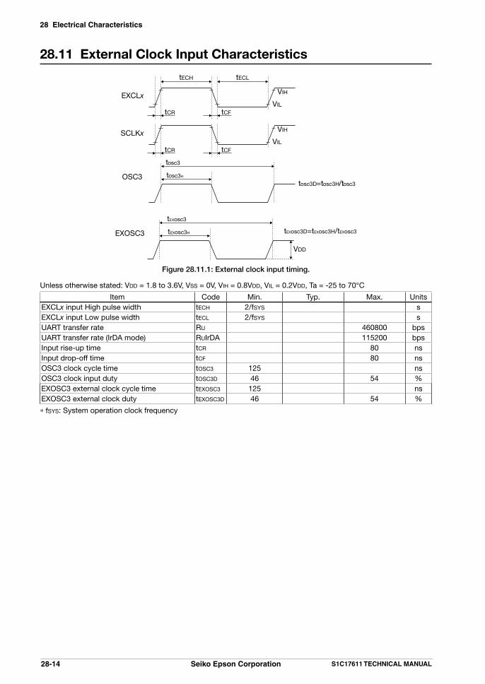
28 Electrical Characteristics
28-14 Seiko Epson Corporation S1C17611 TECHNICAL MANUAL
28.11 External Clock Input Characteristics
EXCLx
tECH tECL
tCFtCR
VIH
VIL
SCLKx
tCFtCR
VIH
VIL
OSC3 tosc3H
tosc3
tosc3D=tosc3H/tosc3
EXOSC3 tEXosc3D=tEXosc3H/tEXosc3tEXosc3H
tEXosc3
VDD
Figure 28.11.1: External clock input timing.
Unless otherwise stated: VDD = 1.8 to 3.6V, VSS = 0V, VIH = 0.8VDD, VIL = 0.2VDD, Ta = -25 to 70°C
Item Code Min. Typ. Max. UnitsEXCLx input High pulse width tECH 2/fSYS sEXCLx input Low pulse width tECL 2/fSYS sUART transfer rate RU 460800 bpsUART transfer rate (IrDA mode) RUIrDA 115200 bpsInput rise-up time tCR 80 nsInput drop-off time tCF 80 nsOSC3 clock cycle time tOSC3 125 nsOSC3 clock input duty tOSC3D 46 54 %EXOSC3 external clock cycle time tEXOSC3 125 nsEXOSC3 external clock duty tEXOSC3D 46 54 %
*fSYS: System operation clock frequency

28 Electrical Characteristics
S1C17611 TECHNICAL MANUAL Seiko Epson Corporation 28-15
28.12 Oscillation Circuit CharacteristicsOscillation characteristics depend on various parameters, including circuit board patterns and the components used. Use the values given for the following characteristics as reference values. For recommended oscillators, see Appendix F.
OSC1 crystal oscillatorUnless otherwise stated: VDD = 1.8 to 3.6V, VSS = 0V, Ta = 25°C, CD1 = Internal, Rf1 = Internal
Item Code Condition Min. Typ. Max. UnitsOscillation start time tsta 3 sExternal gate capacitance CG1 Including board capacitance 0 25 pFInternal drain capacitance CD1 For chip 10 pFFeedback resistor Rf1 10 MW
OSC3 crystal oscillatorUnless otherwise stated: VDD = 1.8 to 3.6V, VSS = 0V, Ta = 25°C, Rf3 = Internal
Item Code Condition Min. Typ. Max. UnitsOscillation start time tsta 20 msFeedback resistor Rf3 1 MW
OSC3 ceramic oscillatorUnless otherwise stated: VDD = 1.8 to 3.6V, VSS = 0V, Ta = 25°C, Rf3 = Internal
Item Code Condition Min. Typ. Max. UnitsOscillation start time tsta 1 msFeedback resistor Rf3 1 MW
IOSC CR oscillatorUnless otherwise stated: VDD = 1.8 to 3.6V, VSS = 0V, Ta = 25°C
Item Code Condition Min. Typ. Max. UnitsOscillation start time tsta 5 µsOscillation frequency fIOSC VD1 = 1.8V 2.16 2.70 3.24 MHz
Oscillation frequency and temperature characteristics
(IOSC) < Internal oscillation >
Typ. value
10000
IIOS
C [k
Hz]
1000-50 -25 0 25 50 75 100
Ta [°C]
Figure 28.12.1

28 Electrical Characteristics
28-16 Seiko Epson Corporation S1C17611 TECHNICAL MANUAL
28.13 R/F Converter Characteristics
Analog characteristicsUnless otherwise stated: VDD = 1.8 V to 3.6 V, VSS = 0 V, Ta = 25°C
Item Code Conditions Min. Typ. Max. UnitStandard oscillation/Sensor oscillation frequency *1
fRFCLK 1 4,000 kHz
Standard oscillation/Sensor oscillation frequency IC deviation *2
∂fRFCLK /∂IC
Resistive sensor DC/AC oscillation mode
VDD=3.6V -25 25 %VDD=1.8V -40 40 %
Capacitive sensor DC oscillation mode
VDD=3.6V -25 25 %VDD=1.8V -50 50 %
Standard resistance/Resistive sensor resistance value *3
RREF, RSEN
Resistive sensor DC/Capacitive sensor DC oscillation mode
1 kW
Resistive sensor AC oscillation mode 10 kWStandard capacitance/Capacitive sensor capacitance value *3
CREF, CSEN
Resistive sensor DC/AC oscillation mode 100 pFCapacitive sensor DC oscillation mode 100 2,000 pF
Time base counter clock frequency fTCCLK 8.2 MHzRFIN pin high level Schmitt input voltage VT+ 0.5•VDD 0.9•VDD VRFIN pin low level Schmitt input voltage VT– 0.1•VDD 0.5•VDD V*1: Setting frequency to 1 kHz or less may incur a larger frequency IC deviation because of variation caused by leak.*2: Deviation includes the dispersion of IC manufacturing and boards in test environments, as well as the variation of
voltage, resistance, and capacitance (excluding variation caused by temperature).*3: The CR oscillation can be generated with resistance and capacitance outside this range (see the following
charts). In that case, however, boards or add-on elements to the IC may induce a larger frequency IC deviation.
RFC Standard oscillation/Sensor oscillation frequency and resistance characteristics
Resistive sensor DC oscillation mode, AC oscillation mode
CREF/CSEN = 1000pF, Ta = 25°C, Typ. value
RFC Standard oscillation/Sensor oscillation frequency and capacitance characteristics
Capacitive sensor DC oscillation mode,
RREF/RSEN = 100 kW, Ta = 25°C, Typ. value
0
1,000
1,000
10,000
10,000 0
1
1
10
10
100
100
fRF
CLK
[kH
z]
VDD=3.6V
IC deviation
VDD=1.8V
RREF/RSEN [kΩ]
1,000
10
100
0
1
10 100 1,000 10,000
fRFC
LK [k
Hz]
CREF/CSEN [pF]
VDD=1.8VVDD=3.6V
IC deviation
Figure 28.13.1 Figure 28.13.2

28 Electrical Characteristics
S1C17611 TECHNICAL MANUAL Seiko Epson Corporation 28-17
RFC Standard oscillation/Sensor oscillation frequency and temperature characteristics
(Resistive sensor DC/AC oscillation mode)
RREF/RSEN = 100 kW, CREF/CSEN = 1000pF Typ. value
RFC standard oscillation/Sensor oscillation frequency and temperature characteristics
(Capacitive sensor DC oscillation mode)
RREF/RSEN = 100 kW, CREF/CSEN = 1000pF Typ. value
-50 -25 0 25 50 75 100Ta [°C]
45 50
2025 30 35 40
0 5
10 15
fRFC
LK [k
Hz]
VDD=1.8V
VDD=3.6V
35 40 45 50
0 5
10 15 20 25 30
fRF
CLK
[kH
z]
VDD=1.8V
Ta [°C]
VDD=3.6V
-50 0 25 50 75-25 100
Figure 28.13.3 Figure 28.13.4
R/F converter current consumption
Unless otherwise stated: VDD = 1.8 to 3.6V, VSS = 0V, Ta = 25°C, TCCLK = 8 MHz, PCKEN = 0x0(OFF)
Item Code Conditions Min. Typ. Max. UnitR/F converter operating current*4
IRFC VDD=3.6V, CREF=CSEN=1000pFRREF=RSEN=100kW
Resistive sensor DC/AC oscillation mode
240 300 µA
Capacitive sensor DC oscillation mode
270 350 µA
*4 The value is added to the current consumption in HALT mode when using the R/F converter. The current consumption varies depending on VDD, standard/senor capacitance, and standard/sensor oscillation frequency.
RFC standard oscillation/Sensor oscillation current consumption and frequency characteristics (Resistive sensor DC/AC oscillation mode)
CREF = 1000pF, Typ. value
RFC standard oscillation/Sensor oscillation current consumption and frequency characteristics
(Capacitive sensor DC oscillation mode)
CREF/CSEN = 1000 pF, Typ. value
2,500
2,000
1,500
IRFC
[µA
]
1,000
500
01 10 100 1,000 10,000
fRFC [kHz]
VDD=3.6V
VDD=1.8V
2,000
1,000
1,500
500
0
IRFC
[µA
]
fRFC [kHz]1 10 100 1,000 10,000
VDD=3.6V
VDD=1.8V
Figure 28.13.5 Figure 28.13.6

29 Basic External Connection Diagram
S1C17611 TECHNICAL MANUAL Seiko Epson Corporation 29-1
29 Basic External Connection Diagram
Example of external components
∗1: Example of resistance sensor DC oscillation connection
SymbolX'tal1CG1
X'tal3Ceramic3RD3
CG3
CD3
CRES
NameCrystal oscillatorTrimmer capacitor or fixed capacitorCrystal oscillatorCeramic oscillatorDrain resistorGate capacitorDrain capacitorPower-on reset capacitor
Recommended value32.768kHz0 to 25pF
0.2 to 8MHz0.2 to 8MHz∗Note∗Note∗Note0.47µF
SymbolCP
C1
C2~4
C5
CREF1
RREF1
RSEN1~2
R3
NameBypass capacitorVD1 stabilizing capacitorVC1-VC3 stabilizing capacitorLCD boosting capacitorBase capacitorBase resistorResistive sensorPull-up resistor
Recommended value3.3µF0.1µF0.1µF0.1µF–––10kΩ
∗Note : For details, refer to Appendix F.
P02/TOUT5/RFCLKOP03/AIN3/SCL0/SCL1P04/AIN2/SDA0/SDA1
P05/AIN1/TOUT4/EXCL3P06/AIN0/FOUT1/LFRO
P14/SIN/#ADTRG/EXCL4P16/SDI/EXCL2
P17/SDO/EXCL1P20/SPICLK/EXCL0/TOUT5
P21/DSIOP22/DST2
S1C17611
LCD Panel 8 × 8 (12 × 4)
[Circuit board potential (chip underside) is VSS.]
VDD
AVDD
TEST1
TEST2
TEST3
OSC1
OSC2
OSC3(P01/OSC3/EXOSC3)∗1
OSC4(P00/OSC4/FOUT1)∗2
VD1
VC1
VC2
VC3
CA
CB
#RESET
VSS
∗1 When OSC3 is set
∗2 When OSC4 is set
P12
(SE
NB
/SC
LK/T
OU
T3)
P11
(SE
NA
/TO
UT4
)
P10
(RE
F/TO
UTN
4)
P07
(RFI
N/F
OU
TH)
VS
SCG1
CP
C1
C2
C3
C4
C5
X'tal1
CRES
RS
EN
2
RS
EN
1
RR
EF1
CR
EF1
+–
SE
G0
SE
G7
CO
M0
CO
M7
I/O
CG3
X'tal3/Ceramic3
CD3
∗1
ICDorI/O
VDD
R3
ICDorOpen
DSIO(P21)DST2(P22)
DCLK
P13(SOUT/FOUTH/TOUTN3)
P15(#SPISS/#BFR/TOUT3)
BUZZER
VDD
RD3

30 Package
S1C17611 TECHNICAL MANUAL Seiko Epson Corporation 30-1
30 PackageQFP12-48pin package
(Units: mm)
Sy
INDEX
48
37
36 25
24
13
121
1.7
1.4
0.1
9
7
97
+0.27-0.130.5
0.081
+0.7-0.3
+0.
2-0
.09
+10
-0

Appendix A: I/O Register List
S1C17611 TECHNICAL MANUAL Seiko Epson Corporation AP-1
Appendix A: I/O Register ListPeripheral circuit Address Register name FunctionPrescaler (8-bit device)
0x4020 PSC_CTL Prescaler Control Register Prescaler start/stop control0x4021~0x403f – – Reserved
UART (with IrDA) (8-bit device)
0x4100 UART_ST UART Status Register Transfer, buffer, error status display0x4101 UART_TXD UART Transmit Data Register Transmission data0x4102 UART_RXD UART Receive Data Register Receiving data0x4103 UART_MOD UART Mode Register Transfer data format setting0x4104 UART_CTL UART Control Register Data transfer control0x4105 UART_EXP UART Expansion Register IrDA mode setting0x4106~0x411f – – Reserved
8-bit timer (with F mode) (16-bit device)
0x4200 T8F_CLK 8-bit Timer Input Clock Select Register Prescaler output clock selection0x4202 T8F_TR 8-bit Timer Reload Data Register Reload data setting0x4204 T8F_TC 8-bit Timer Counter Data Register Counter data0x4206 T8F_CTL 8-bit Timer Control Register Timer mode setting and timer RUN/STOP0x4208 T8F_INT 8-bit Timer Interrupt Control Register Interrupt control0x420a~0x421f – – Reserved
16-bit timer Ch.0 (16-bit device)
0x4220 T16_CLK0 16-bit Timer Ch.0 Input Clock Select Register Prescaler output clock selection0x4222 T16_TR0 16-bit Timer Ch.0 Reload Data Register Reload data setting0x4224 T16_TC0 16-bit Timer Ch.0 Counter Data Register Counter data0x4226 T16_CTL0 16-bit Timer Ch.0 Control Register Timer mode setting and timer RUN/STOP0x4228 T16_INT0 16-bit Timer Ch.0 Interrupt Control Register Interrupt control0x422a~0x423f – – Reserved
16-bit timer Ch.1 (16-bit device)
0x4240 T16_CLK1 16-bit Timer Ch.1 Input Clock Select Register Prescaler output clock selection0x4242 T16_TR1 16-bit Timer Ch.1 Reload Data Register Reload data setting0x4244 T16_TC1 16-bit Timer Ch.1 Counter Data Register Counter data0x4246 T16_CTL1 16-bit Timer Ch.1 Control Register Timer mode setting and timer RUN/STOP0x4248 T16_INT1 16-bit Timer Ch.1 Interrupt Control Register Interrupt control0x424a~0x425f – – Reserved
16-bit timer Ch.2 (16-bit device)
0x4260 T16_CLK2 16-bit Timer Ch.2 Input Clock Select Register Prescaler output clock selection0x4262 T16_TR2 16-bit Timer Ch.2 Reload Data Register Reload data setting0x4264 T16_TC2 16-bit Timer Ch.2 Counter Data Register Counter data0x4266 T16_CTL2 16-bit Timer Ch.2 Control Register Timer mode setting and timer RUN/STOP0x4268 T16_INT2 16-bit Timer Ch.2 Interrupt Control Register Interrupt control0x426a~0x427f – – Reserved
Interrupt controller (16-bit device)
0x4300~0x4304 – – Reserved0x4306 ITC_LV0 Interrupt Level Setup Register 0 P0/P1 interrupt level setting0x4308 ITC_LV1 Interrupt Level Setup Register 1 SWT/CT interrupt level setting0x430a ITC_LV2 Interrupt Level Setup Register 2 T8OSC1/SVD interrupt level setting0x430c ITC_LV3 Interrupt Level Setup Register 3 LCD/T16E Ch.0 interrupt level setting0x430e ITC_LV4 Interrupt Level Setup Register 4 T8F/T16 Ch.0 interrupt level setting0x4310 ITC_LV5 Interrupt Level Setup Register 5 T16 Ch.1/Ch.2 interrupt level setting0x4312 ITC_LV6 Interrupt Level Setup Register 6 UART/I2CS interrupt level setting0x4314 ITC_LV7 Interrupt Level Setup Register 7 SPI/I2CM interrupt level setting0x4316 ITC_LV8 Interrupt Level Setup Register 8 T16E Ch.1 interrupt level setting0x4318 ITC_LV9 Interrupt Level Setup Register 9 ADC10SA/RFC interrupt setting0x431a~0x431f – – Reserved
SPI (16-bit device)
0x4320 SPI_ST SPI Status Register Transfer and buffer status display0x4322 SPI_TXD SPI Transmit Data Register Transmission data0x4324 SPI_RXD SPI Receive Data Register Receiving data0x4326 SPI_CTL SPI Control Register SPI mode and data transfer permission setting0x4328~0x433f – – Reserved
I2C (master)(16-bit device)
0x4340 I2C_EN I2C Enable Register I2C module enable0x4342 I2C_CTL I2C Control Register I2C control and transfer status display0x4344 I2C_DAT I2C Data Register Transfer data0x4346 I2C_ICTL I2C Interrupt Control Register I2C interrupt control0x4348~0x435f – – Reserved

Appendix A: I/O Register List
AP-2 Seiko Epson Corporation S1C17611 TECHNICAL MANUAL
Peripheral circuit Address Register name FunctionI2C (slave)(16-bit device)
0x4360 I2CS_TRNS I2C Slave Transfer Data Write Register I2C slave transmission data0x4362 I2CS_RECV I2C Slave Receive Data Read Register I2C slave receiving data0x4364 I2CS_SADRS I2C Slave Address Set Register I2C slave address setting0x4366 I2CS_CTL I2C Slave Control Register I2C slave control0x4368 I2CS_STAT I2C Slave Status Register I2C slave bus status display0x436a I2CS_ASTAT I2C Slave Access Status Register I2C slave access status display0x436c I2CS_ICTL I2C Slave Interrupt Control Register I2C slave interrupt control0x4370~0x437f – – Reserved
Clock timer (8-bit device)
0x5000 CT_CTL Clock Timer Control Register Timer reset and RUN/STOP control0x5001 CT_CNT Clock Timer Counter Register Counter data0x5002 CT_IMSK Clock Timer Interrupt Mask Register Interrupt mask setting0x5003 CT_IFLG Clock Timer Interrupt Flag Register Interrupt occurrence status display/reset0x5004~0x501f – – Reserved
Stopwatch timer (8-bit device)
0x5020 SWT_CTL Stopwatch Timer Control Register Timer reset and RUN/STOP control0x5021 SWT_BCNT Stopwatch Timer BCD Counter Register BCD counter data0x5022 SWT_IMSK Stopwatch Timer Interrupt Mask Register Interrupt mask setting0x5023 SWT_IFLG Stopwatch Timer Interrupt Flag Register Interrupt occurrence status display/reset0x5024~0x503f – – Reserved
Watchdog timer (8-bit device)
0x5040 WDT_CTL Watchdog Timer Control Register Timer reset and RUN/STOP control0x5041 WDT_ST Watchdog Timer Status Register Timer mode setting and NMI status display0x5042~0x505f – – Reserved
Oscillator circuit (8-bit device)
0x5060 OSC_SRC Clock Source Select Register Clock source selection0x5061 OSC_CTL Oscillation Control Register Oscillation control0x5062 OSC_NFEN Noise Filter Enable Register Noise filter ON/OFF0x5063 OSC_LCLK LCD Clock Setup Register LCD clock setting0x5064 OSC_FOUT FOUT Control Register Clock external output control0x5065 OSC_T8OSC1 T8OSC1 Clock Control Register 8-bit OSC1 timer clock setting0x5066 OSC_SVD SVD Clock Control Register SVD clock setting0x5067 OSC_RFTCK RFC TC Clock Control Register RFC TC clock setting0x5068~0x507f – – Reserved
Clock generator (8-bit device)
0x5080 CLG_PCLK PCLK Control Register PCLK feed control0x5081 CLG_CCLK CCLK Control Register CCLK division ratio setting0x5082~0x509f – – Reserved
LCD driver (8-bit device)
0x50a0 LCD_DCTL LCD Display Control Register LCD display control0x50a1 LCD_CADJ LCD Contrast Adjust Register Contrast control0x50a2 LCD_CCTL LCD Clock Control Register LCD clock duty selection0x50a3 LCD_VREG LCD Voltage Regulator Control Register LCD driver constant-voltage circuit control0x50a4 – – Reserved0x50a5 LCD_IMSK LCD Interrupt Mask Register Interrupt mask setting0x50a6 LCD_IFLG LCD Interrupt Flag Register Interrupt occurrence status display/reset0x50a7~0x50bf – – Reserved
8-bit OSC1 timer (8-bit device)
0x50c0 T8OSC1_CTL 8-bit OSC1 Timer Control Register Timer mode setting and timer RUN/STOP0x50c1 T8OSC1_CNT 8-bit OSC1 Timer Counter Data Register Counter data0x50c2 T8OSC1_CMP 8-bit OSC1 Timer Compare Data Register Compare data setting0x50c3 T8OSC1_IMSK 8-bit OSC1 Timer Interrupt Mask Register Interrupt mask setting0x50c4 T8OSC1_IFLG 8-bit OSC1 Timer Interrupt Flag Register Interrupt occurrence status display/reset0x50c5 T8OSC1_DUTY 8-bit OSC1 Timer PWM Data Register PWM output data setting0x50c6~0x50df – – Reserved
SVD circuit (8-bit device)
0x5100 SVD_EN SVD Enable Register SVD operation permitted/prevented0x5101 SVD_CMP SVD Compare Voltage Register Comparison voltage setting0x5102 SVD_RSLT SVD Detection Result Register Voltage detection results0x5103 SVD_IMSK SVD Interrupt Mask Register Interrupt mask setting0x5104 SVD_IFLG SVD Interrupt Flag Register Interrupt occurrence status display/reset0x5105~0x511f – – Reserved
Power supply circuit(8-bit device)
0x5120 VD1_CTL VD1 Control Register VD1 voltage and load protection control0x5121~0x513f – – Reserved

Appendix A: I/O Register List
S1C17611 TECHNICAL MANUAL Seiko Epson Corporation AP-3
Peripheral circuit Address Register name FunctionP port & port MUX (8-bit device)
0x5200 P0_IN P0 Port Input Data Register P0 port input data0x5201 P0_OUT P0 Port Output Data Register P0 port output data0x5202 P0_OEN P0 Port Output Enable Register P0 port output enable0x5203 P0_PU P0 Port Pull-up Control Register P0 port pull-up control0x5204 P0_SM P0 Port Schmitt Trigger Control Register P0 port Schmitt trigger control0x5205 P0_IMSK P0 Port Interrupt Mask Register P0 port interrupt mask setting0x5206 P0_EDGE P0 Port Interrupt Edge Select Register P0 port interrupt edge selection0x5207 P0_IFLG P0 Port Interrupt Flag Register P0 port interrupt occurrence status display/reset0x5208 P0_CHAT P0 Port Chattering Filter Control Register P0 port chattering filter control0x5209 P0_KRST P0 Port Key-Entry Reset Configuration Register P0 port key entry reset setting0x520a P0_IEN P0 Port Input Enable Register P0 port input enable0x520b~0x520f – – Reserved0x5210 P1_IN P1 Port Input Data Register P1 port input data0x5211 P1_OUT P1 Port Output Data Register P1 port output data0x5212 P1_OEN P1 Port Output Enable Register P1 port output enable0x5213 P1_PU P1 Port Pull-up Control Register P1 port pull-up control0x5214 P1_SM P1 Port Schmitt Trigger Control Register P1 port Schmitt trigger control0x5215 P1_IMSK P1 Port Interrupt Mask Register P1 port interrupt mask setting0x5216 P1_EDGE P1 Port Interrupt Edge Select Register P1 port interrupt edge selection0x5217 P1_IFLG P1 Port Interrupt Flag Register P1 port interrupt occurrence status display/reset0x5218 P1_CHAT P1 Port Chattering Filter Control Register P1 port chattering filter control0x5219 – – Reserved0x521a P1_IEN P1 Port Input Enable Register P1 port input enable0x521b~0x521f – – Reserved0x5220 P2_IN P2 Port Input Data Register P2 port input data0x5221 P2_OUT P2 Port Output Data Register P2 port output data0x5222 P2_OEN P2 Port Output Enable Register P2 port output enable0x5223 P2_PU P2 Port Pull-up Control Register P2 port pull-up control0x5224 P2_SM P2 Port Schmitt Trigger Control Register P2 port Schmitt trigger control0x5225~0x5229 – – Reserved0x522a P2_IEN P2 Port Input Enable Register P2 port input enable0x522b~0x527f – – Reserved0x52a0~0x52a1 P0_PMUX P0 Port Function Select Register P0 port function selection0x52a2~0x52a3 P1_PMUX P1 Port Function Select Register P1 port function selection0x52a4 P2_PMUX P2 Port Function Select Register P2 port function selection0x52a5~0x52bf – – Reserved
PWM timer Ch.0(16-bit device)
0x5300 T16E_CA0 PWM Timer Ch.0 Compare Data A Register Compare data A setting0x5302 T16E_CB0 PWM Timer Ch.0 Compare Data B Register Compare data B setting0x5304 T16E_TC0 PWM Timer Ch.0 Counter Data Register Counter data0x5306 T16E_CTL0 PWM Timer Ch.0 Control Register Timer mode setting and timer RUN/STOP0x5308 T16E_CLK0 PWM Timer Ch.0 Input Clock Select Register Prescaler output clock selection0x530a T16E_IMSK0 PWM Timer Ch.0 Interrupt MASK Register Interrupt factor mask selection0x530c T16E_IFLG0 PWM Timer Ch.0 Interrupt Flag Register Interrupt factor checking0x530e~0x531f – – Reserved
MISC register (16-bit device)
0x5320 MISC_FL FLASHC/SRAMC Control Register FLASHC/SRAMC access condition setting0x5322 MISC_OSC1 OSC1 Peripheral Control Register OSC1 operation peripheral function setting
for debugging0x5324 MISC_PROT MISC Protect Register MISC register write protection0x5326 MISC_IRAMSZ IRAM Size Select Register IRAM size selection0x5328 MISC_TTBRL Vector Table Address Low Register Vector table address setting0x532a MISC_TTBRH Vector Table Address High Register Vector table address setting0x532c MISC_PSR PSR Register PSR Readout0x532e~0x533f – – Reserved
PWM timer Ch.1(16-bit device)
0x5360 T16E_CA1 PWM Timer Ch.1 Compare Data A Register Compare data A setting0x5362 T16E_CB1 PWM Timer Ch.1 Compare Data B Register Compare data B setting0x5364 T16E_TC1 PWM Timer Ch.1 Counter Data Register Counter data0x5366 T16E_CTL1 PWM Timer Ch.1 Control Register Timer mode setting and timer RUN/STOP0x5368 T16E_CLK1 PWM Timer Ch.1 Input Clock Select Register Prescaler output clock selection0x536a T16E_IMSK1 PWM Timer Ch.1 Interrupt MASK Register Interrupt factor mask selection0x536c T16E_IFLG1 PWM Timer Ch.1 Interrupt Flag Register Interrupt factor checking
A/D converter(16-bit device)
0x5380 ADC10_ADD ADC10 Conversion Result Register A/D conversion result0x5382 ADC10_TRG ADC10 Trigger/Channel Select Register Conversion Trigger/channel setting0x5384 ADC10_CTL ADC10 Control/Status Register Conversion control/status0x5386 ADC10_DIV ADC10 divided frequency Register A/D conversion clock divided frequency
setting0x5388~0x539f – – Reserved

Appendix A: I/O Register List
AP-4 Seiko Epson Corporation S1C17611 TECHNICAL MANUAL
Peripheral circuit Address Register name FunctionR/F converter(16-bit device)
0x53a0 RFC_CTL RFC Control Register R/F converter setting0x53a2 RFC_TRG RFC Oscillation Trigger Register R/F oscillation starting trigger0x53a4 RFC_MCL RFC Measurement Counter Data Register (LSB) Measurement counter (lower)0x53a6 RFC_MCH RFC Measurement Counter Data Register (MSB) Measurement counter (upper)0x53a8 RFC_TCL RFC Time Base Counter Data Register (LSB) Time base couner (lower)0x53aa RFC_TCH RFC Time Base Counter Data Register (MSB) Time base couner (upper)0x53ac RFC_IMSK RFC Interrupt Mask Register Interrupt mask setting0x53ae RFC_IFLG RFC Interrupt Flag Register Interrupt flag0x53b0~0x53bf – – Reserved
SEGRAM(16-bit device)
0x53c0~0x53cb SEGRAM SEGRAM Data Segram data0x53cc~0x53ff – – Reserved
S1C17 core I/O 0xffff84 IDIR Processor ID Register Processor ID display0xffff90 DBRAM Debug RAM Base Register Debugging RAM base address display0xffffa0 DCR Debug Control Register Debug control0xffffb8 IBAR2 Instruction Break Address Register 2 Instruction break address #2 setting0xffffbc IBAR3 Instruction Break Address Register 3 Instruction break address #3 setting0xffffd0 IBAR4 Instruction Break Address Register 4 Instruction break address #4 setting
Note: Addresses marked as “Reserved” or unused peripheral circuit areas not marked in the table must not be accessed by application programs.

Appendix A: I/O Register List
S1C17611 TECHNICAL MANUAL Seiko Epson Corporation AP-5
0x4020 Prescaler
Register name Address Bit Name Function Setting Init. R/W Remarks
Prescaler Control Register(PSC_CTL)
0x4020(8 bits)
D7–2 – reserved – – – 0 when being read.D1 PRUND Prescaler run/stop in debug mode 1 Run 0 Stop 0 R/WD0 PRUN Prescaler run/stop control 1 Run 0 Stop 0 R/W

Appendix A: I/O Register List
AP-6 Seiko Epson Corporation S1C17611 TECHNICAL MANUAL
0x4100–0x4105 UART (with IrDA)
Register name Address Bit Name Function Setting Init. R/W Remarks
UART Status Register(UART_ST)
0x4100(8 bits)
D7 – reserved – – – 0 when being read.D6 FER Framing error flag 1 Error 0 Normal 0 R/W Reset by writing 1.D5 PER Parity error flag 1 Error 0 Normal 0 R/WD4 OER Overrun error flag 1 Error 0 Normal 0 R/WD3 RD2B Second byte receive flag 1 Ready 0 Empty 0 RD2 TRBS Transmit busy flag 1 Busy 0 Idle 0 R Shift register statusD1 RDRY Receive data ready flag 1 Ready 0 Empty 0 RD0 TDBE Transmit data buffer empty flag 1 Empty 0 Not empty 1 R
UART Transmit Data Register(UART_TXD)
0x4101(8 bits)
D7–0 TXD[7:0] Transmit dataTXD7(6) = MSBTXD0 = LSB
0x0 to 0xff (0x7f) 0x0 R/W
UART Receive Data Register(UART_RXD)
0x4102(8 bits)
D7–0 RXD[7:0] Receive data in the receive data bufferRXD7(6) = MSBRXD0 = LSB
0x0 to 0xff (0x7f) 0x0 R Older data in the buffer is read out first.
UART Mode Register(UART_MOD)
0x4103(8 bits)
D7–5 – reserved – – – 0 when being read.D4 CHLN Character length 1 8 bits 0 7 bits 0 R/WD3 PREN Parity enable 1 With parity 0 No parity 0 R/WD2 PMD Parity mode select 1 Odd 0 Even 0 R/WD1 STPB Stop bit select 1 2 bits 0 1 bit 0 R/WD0 SSCK Input clock select 1 External 0 Internal 0 R/W
UART Control Register(UART_CTL)
0x4104(8 bits)
D7 – reserved – – – 0 when being read.D6 REIEN Receive error int. enable 1 Enable 0 Disable 0 R/WD5 RIEN Receive buffer full int. enable 1 Enable 0 Disable 0 R/WD4 TIEN Transmit buffer empty int. enable 1 Enable 0 Disable 0 R/W
D3–2 – reserved – – – 0 when being read.D1 RBFI Receive buffer full int. condition 1 2 bytes 0 1 byte 0 R/WD0 RXEN UART enable 1 Enable 0 Disable 0 R/W
UART Expansion Register(UART_EXP)
0x4105(8 bits)
D7 – reserved – – – 0 when being read.D6–4 IRCLK[2:0] IrDA receive detection clock
selectIRCLK[2:0] Clock 0x0 R/W
0x70x60x50x40x30x20x10x0
PCLK•1/128PCLK•1/64PCLK•1/32PCLK•1/16PCLK•1/8PCLK•1/4PCLK•1/2PCLK•1/1
D3–1 – reserved – – – 0 when being read.D0 IRMD IrDA mode select 1 On 0 Off 0 R/W

Appendix A: I/O Register List
S1C17611 TECHNICAL MANUAL Seiko Epson Corporation AP-7
0x4200–0x4208 8-bit Timer (with Fine Mode)
Register name Address Bit Name Function Setting Init. R/W Remarks
8-bit Timer Input Clock Select Register(T8F_CLK)
0x4200(16 bits)
D15–4 – reserved – – – 0 when being read.D3–0 DF[3:0] 8-bit timer input clock select
(Prescaler output clock)DF[3:0] Clock 0x0 R/W
0xf0xe0xd0xc0xb0xa0x90x80x70x60x50x40x30x20x10x0
reservedPCLK•1/16384PCLK•1/8192PCLK•1/4096PCLK•1/2048PCLK•1/1024PCLK•1/512PCLK•1/256PCLK•1/128PCLK•1/64PCLK•1/32PCLK•1/16PCLK•1/8PCLK•1/4PCLK•1/2PCLK•1/1
8-bit Timer Reload Data Register(T8F_TR)
0x4202(16 bits)
D15–8 – reserved – – – 0 when being read.D7–0 TR[7:0] 8-bit timer reload data
TR7 = MSBTR0 = LSB
0x0 to 0xff 0x0 R/W
8-bit Timer Counter Data Register(T8F_TC)
0x4204(16 bits)
D15–8 – reserved – – – 0 when being read.D7–0 TC[7:0] 8-bit timer counter data
TC7 = MSBTC0 = LSB
0x0 to 0xff 0xff R
8-bit Timer Control Register(T8F_CTL)
0x4206(16 bits)
D15–12 – reserved – – – 0 when being read.D11–8 TFMD[3:0] Fine mode setup 0x0 to 0xf 0x0 R/W Set a number of times
to insert delay into a 16-underflow period.
D7–5 – reserved – – – 0 when being read.D4 TRMD Count mode select 1 One shot 0 Repeat 0 R/W
D3–2 – reserved – – – 0 when being read.D1 PRESER Timer reset 1 Reset 0 Ignored 0 WD0 PRUN Timer run/stop control 1 Run 0 Stop 0 R/W
8-bit TimerInterrupt Control Register(T8F_INT)
0x4208(16 bits)
D15–9 – reserved – – – 0 when being read.D8 T8IE 8-bit timer interrupt enable 1 Enable 0 Disable 0 R/W
D7–1 – reserved – – – 0 when being read.D0 T8IF 8-bit timer interrupt flag 1 Cause of
interrupt occurred
0 Cause of interrupt not occurred
0 R/W Reset by writing 1.

Appendix A: I/O Register List
AP-8 Seiko Epson Corporation S1C17611 TECHNICAL MANUAL
0x4220–0x4244 16-bit Timer
Register name Address Bit Name Function Setting Init. R/W Remarks
16-bit Timer Ch.0 Input Clock Select Register(T16_CLK0)
0x4220(16 bits)
D15–4 – reserved – – – 0 when being read.D3–0 DF[3:0] Timer input clock select
(Prescaler output clock)DF[3:0] Clock 0x0 R/W
0xf0xe0xd0xc0xb0xa0x90x80x70x60x50x40x30x20x10x0
reservedPCLK•1/16384PCLK•1/8192PCLK•1/4096PCLK•1/2048PCLK•1/1024PCLK•1/512PCLK•1/256PCLK•1/128PCLK•1/64PCLK•1/32PCLK•1/16PCLK•1/8PCLK•1/4PCLK•1/2PCLK•1/1
16-bit Timer Ch.0 Reload Data Register(T16_TR0)
0x4222(16 bits)
D15–0 TR[15:0] 16-bit timer reload dataTR15 = MSBTR0 = LSB
0x0 to 0xffff 0x0 R/W
16-bit Timer Ch.0 Counter Data Register(T16_TC0)
0x4224(16 bits)
D15–0 TC[15:0] 16-bit timer counter dataTC15 = MSBTC0 = LSB
0x0 to 0xffff 0xffff R
16-bit Timer Ch.0 Control Register(T16_CTL0)
0x4226(16 bits)
D15–11 – reserved – – – 0 when being read.D10 CKACTV External clock active level select 1 High 0 Low 1 R/WD9–8 CKSL[1:0] Input clock and pulse width
measurement mode selectCKSL[1:0] Mode 0x0 R/W
0x30x20x10x0
reservedPulse width
External clockInternal clock
D7–5 – reserved – – – 0 when being read.D4 TRMD Count mode select 1 One shot 0 Repeat 0 R/W
D3–2 – reserved – – – 0 when being read.D1 PRESER Timer reset 1 Reset 0 Ignored 0 WD0 PRUN Timer run/stop control 1 Run 0 Stop 0 R/W
16-bit Timer Ch.0 Interrupt Control Register(T16_INT0)
0x4228(16 bits)
D15–9 – reserved – – – 0 when being read.D8 T16IE 16-bit timer interrupt enable 1 Enable 0 Disable 0 R/W
D7–1 – reserved – – – 0 when being read.D0 T16IF 16-bit timer interrupt flag 1 Cause of
interrupt occurred
0 Cause of interrupt not occurred
0 R/W Reset by writing 1.
16-bit Timer Ch.1 Input Clock Select Register(T16_CLK1)
0x4240(16 bits)
D15–4 – reserved – – – 0 when being read.D3–0 DF[3:0] Timer input clock select
(Prescaler output clock)DF[3:0] Clock 0x0 R/W
0xf0xe0xd0xc0xb0xa0x90x80x70x60x50x40x30x20x10x0
reservedPCLK•1/16384PCLK•1/8192PCLK•1/4096PCLK•1/2048PCLK•1/1024PCLK•1/512PCLK•1/256PCLK•1/128PCLK•1/64PCLK•1/32PCLK•1/16PCLK•1/8PCLK•1/4PCLK•1/2PCLK•1/1
16-bit Timer Ch.1 Reload Data Register(T16_TR1)
0x4242(16 bits)
D15–0 TR[15:0] 16-bit timer reload dataTR15 = MSBTR0 = LSB
0x0 to 0xffff 0x0 R/W
16-bit Timer Ch.1 Counter Data Register(T16_TC1)
0x4244(16 bits)
D15–0 TC[15:0] 16-bit timer counter dataTC15 = MSBTC0 = LSB
0x0 to 0xffff 0xffff R
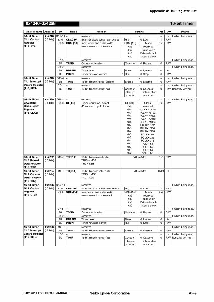
Appendix A: I/O Register List
S1C17611 TECHNICAL MANUAL Seiko Epson Corporation AP-9
0x4246–0x4268 16-bit Timer
Register name Address Bit Name Function Setting Init. R/W Remarks
16-bit Timer Ch.1 Control Register(T16_CTL1)
0x4246(16 bits)
D15–11 – reserved – – – 0 when being read.D10 CKACTV External clock active level select 1 High 0 Low 1 R/WD9–8 CKSL[1:0] Input clock and pulse width
measurement mode selectCKSL[1:0] Mode 0x0 R/W
0x30x20x10x0
reservedPulse width
External clockInternal clock
D7–5 – reserved – – – 0 when being read.D4 TRMD Count mode select 1 One shot 0 Repeat 0 R/W
D3–2 – reserved – – – 0 when being read.D1 PRESER Timer reset 1 Reset 0 Ignored 0 WD0 PRUN Timer run/stop control 1 Run 0 Stop 0 R/W
16-bit Timer Ch.1 Interrupt Control Register(T16_INT1)
0x4248(16 bits)
D15–9 – reserved – – – 0 when being read.D8 T16IE 16-bit timer interrupt enable 1 Enable 0 Disable 0 R/W
D7–1 – reserved – – – 0 when being read.D0 T16IF 16-bit timer interrupt flag 1 Cause of
interrupt occurred
0 Cause of interrupt not occurred
0 R/W Reset by writing 1.
16-bit Timer Ch.2 Input Clock Select Register(T16_CLK2)
0x4260(16 bits)
D15–4 – reserved – – – 0 when being read.D3–0 DF[3:0] Timer input clock select
(Prescaler output clock)DF[3:0] Clock 0x0 R/W
0xf0xe0xd0xc0xb0xa0x90x80x70x60x50x40x30x20x10x0
reservedPCLK•1/16384PCLK•1/8192PCLK•1/4096PCLK•1/2048PCLK•1/1024PCLK•1/512PCLK•1/256PCLK•1/128PCLK•1/64PCLK•1/32PCLK•1/16PCLK•1/8PCLK•1/4PCLK•1/2PCLK•1/1
16-bit Timer Ch.2 Reload Data Register(T16_TR2)
0x4262(16 bits)
D15–0 TR[15:0] 16-bit timer reload dataTR15 = MSBTR0 = LSB
0x0 to 0xffff 0x0 R/W
16-bit Timer Ch.2 Counter Data Register(T16_TC2)
0x4264(16 bits)
D15–0 TC[15:0] 16-bit timer counter dataTC15 = MSBTC0 = LSB
0x0 to 0xffff 0xffff R
16-bit Timer Ch.2 Control Register(T16_CTL2)
0x4266(16 bits)
D15–11 – reserved – – – 0 when being read.D10 CKACTV External clock active level select 1 High 0 Low 1 R/WD9–8 CKSL[1:0] Input clock and pulse width
measurement mode selectCKSL[1:0] Mode 0x0 R/W
0x30x20x10x0
reservedPulse width
External clockInternal clock
D7–5 – reserved – – – 0 when being read.D4 TRMD Count mode select 1 One shot 0 Repeat 0 R/W
D3–2 – reserved – – – 0 when being read.D1 PRESER Timer reset 1 Reset 0 Ignored 0 WD0 PRUN Timer run/stop control 1 Run 0 Stop 0 R/W
16-bit Timer Ch.2 Interrupt Control Register(T16_INT2)
0x4268(16 bits)
D15–9 – reserved – – – 0 when being read.D8 T16IE 16-bit timer interrupt enable 1 Enable 0 Disable 0 R/W
D7–1 – reserved – – – 0 when being read.D0 T16IF 16-bit timer interrupt flag 1 Cause of
interrupt occurred
0 Cause of interrupt not occurred
0 R/W Reset by writing 1.

Appendix A: I/O Register List
AP-10 Seiko Epson Corporation S1C17611 TECHNICAL MANUAL
0x4306–0x4318 Interrupt Controller
Register name Address Bit Name Function Setting Init. R/W Remarks
Interrupt Level Setup Register 0(ITC_LV0)
0x4306(16 bits)
D15–11 – reserved – – – 0 when being read.D10–8 ILV1[2:0] P1 interrupt level 0 to 7 0x0 R/WD7–3 – reserved – – – 0 when being read.D2–0 ILV0[2:0] P0 interrupt level 0 to 7 0x0 R/W
Interrupt Level Setup Register 1(ITC_LV1)
0x4308(16 bits)
D15–11 – reserved – – – 0 when being read.D10–8 ILV3[2:0] CT interrupt level 0 to 7 0x0 R/WD7–3 – reserved – – – 0 when being read.D2–0 ILV2[2:0] SWT interrupt level 0 to 7 0x0 R/W
Interrupt Level Setup Register 2(ITC_LV2)
0x430a(16 bits)
D15–11 – reserved – – – 0 when being read.D10–8 ILV5[2:0] SVD interrupt level 0 to 7 0x0 R/WD7–3 – reserved – – – 0 when being read.D2–0 ILV4[2:0] T8OSC1 interrupt level 0 to 7 0x0 R/W
Interrupt Level Setup Register 3(ITC_LV3)
0x430c(16 bits)
D15–11 – reserved – – – 0 when being read.D10–8 ILV7[2:0] T16E Ch.0 interrupt level 0 to 7 0x0 R/WD7–3 – reserved – – – 0 when being read.D2–0 ILV6[2:0] LCD interrupt level 0 to 7 0x0 R/W
Interrupt Level Setup Register 4(ITC_LV4)
0x430e(16 bits)
D15–11 – reserved – – – 0 when being read.D10–8 ILV9[2:0] T16 Ch.0 interrupt level 0 to 7 0x0 R/WD7–3 – reserved – – – 0 when being read.D2–0 ILV8[2:0] T8F interrupt level 0 to 7 0x0 R/W
Interrupt Level Setup Register 5(ITC_LV5)
0x4310(16 bits)
D15–11 – reserved – – – 0 when being read.D10–8 ILV11[2:0] T16 Ch.2 interrupt level 0 to 7 0x0 R/WD7–3 – reserved – – – 0 when being read.D2–0 ILV10[2:0] T16 Ch.1 interrupt level 0 to 7 0x0 R/W
Interrupt Level Setup Register 6(ITC_LV6)
0x4312(16 bits)
D15–11 – reserved – – – 0 when being read.D10–8 ILV13[2:0] I2C slave interrupt level 0 to 7 0x0 R/WD7–3 – reserved – – – 0 when being read.D2–0 ILV12[2:0] UART interrupt level 0 to 7 0x0 R/W
Interrupt Level Setup Register 7(ITC_LV7)
0x4314(16 bits)
D15–11 – reserved – – – 0 when being read.D10–8 ILV15[2:0] I2C Master interrupt level 0 to 7 0x0 R/WD7–3 – reserved – – – 0 when being read.D2–0 ILV14[2:0] SPI interrupt level 0 to 7 0x0 R/W
Interrupt Level Setup Register 8(ITC_LV8)
0x4316(16 bits)
D15–3 – reserved – – – 0 when being read.D2–0 ILV16[2:0] T16E Ch.1 interrupt level 0 to 7 0x0 R/W
Interrupt Level Setup Register 9(ITC_LV9)
0x4318(16 bits)
D15–11 – reserved – – – 0 when being read.D10–8 ILV19[2:0] RFC interrupt level 0 to 7 0x0 R/WD7–3 – reserved – – – 0 when being read.D2–0 ILV18[2:0] ADC10SA interrupt level 0 to 7 0x0 R/W

Appendix A: I/O Register List
S1C17611 TECHNICAL MANUAL Seiko Epson Corporation AP-11
0x4320–0x4326 SPI
Register name Address Bit Name Function Setting Init. R/W Remarks
SPI Status Register(SPI_ST)
0x4320(16 bits)
D15–3 – reserved – – – 0 when being read.D2 SPBSY Transfer busy flag (master) 1 Busy 0 Idle 0 R
ss signal low flag (slave) 1 ss = L 0 ss = HD1 SPRBF Receive data buffer full flag 1 Full 0 Not full 0 RD0 SPTBE Transmit data buffer empty flag 1 Empty 0 Not empty 1 R
SPI Transmit Data Register(SPI_TXD)
0x4322(16 bits)
D15–8 – reserved – – – 0 when being read.D7–0 SPTDB[7:0] SPI transmit data buffer
SPTDB7 = MSBSPTDB0 = LSB
0x0 to 0xff 0x0 R/W
SPI Receive Data Register(SPI_RXD)
0x4324(16 bits)
D15–8 – reserved – – – 0 when being read.D7–0 SPRDB[7:0] SPI receive data buffer
SPRDB7 = MSBSPRDB0 = LSB
0x0 to 0xff 0x0 R
SPI Control Register(SPI_CTL)
0x4326(16 bits)
D15–10 – reserved – – – 0 when being read.D9 MCLK SPI clock source select 1 T16 Ch.1 0 PCLK•1/4 0 R/WD8 MLSB LSB/MSB first mode select 1 LSB 0 MSB 0 R/W
D7–6 – reserved – – – 0 when being read.D5 SPRIE Receive data buffer full int. enable 1 Enable 0 Disable 0 R/WD4 SPTIE Transmit data buffer empty int. enable 1 Enable 0 Disable 0 R/WD3 CPHA Clock phase select 1 Data out 0 Data in 0 R/W These bits must be
set before setting SPEN to 1.
D2 CPOL Clock polarity select 1 Active L 0 Active H 0 R/WD1 MSSL Master/slave mode select 1 Master 0 Slave 0 R/WD0 SPEN SPI enable 1 Enable 0 Disable 0 R/W

Appendix A: I/O Register List
AP-12 Seiko Epson Corporation S1C17611 TECHNICAL MANUAL
0x4340–0x4346 I2C Master
Register name Address Bit Name Function Setting Init. R/W Remarks
I2C Enable Register(I2C_EN)
0x4340(16 bits)
D15–1 – reserved – – – 0 when being read.
D0 I2CEN I2C enable 1 Enable 0 Disable 0 R/W
I2C Control Register(I2C_CTL)
0x4342(16 bits)
D15–10 – reserved – – – 0 when being read.D9 RBUSY Receive busy flag 1 Busy 0 Idle 0 RD8 TBUSY Transmit busy flag 1 Busy 0 Idle 0 R
D7–5 – reserved – – – 0 when being read.D4 NSERM Noise remove on/off 1 On 0 Off 0 R/W
D3–2 – reserved – – – 0 when being read.D1 STP Stop control 1 Stop 0 Ignored 0 R/WD0 STRT Start control 1 Start 0 Ignored 0 R/W
I2C Data Register(I2C_DAT)
0x4344(16 bits)
D15–12 – reserved – – – 0 when being read.D11 RBRDY Receive buffer ready 1 Ready 0 Empty 0 RD10 RXE Receive execution 1 Receive 0 Ignored 0 R/WD9 TXE Transmit execution 1 Transmit 0 Ignored 0 R/WD8 RTACK Receive/transmit ACK 1 Error 0 ACK 0 R/W
D7–0 RTDT[7:0] Receive/transmit dataRTDT7 = MSBRTDT0 = LSB
0x0 to 0xff 0x0 R/W
I2C Interrupt Control Register(I2C_ICTL)
0x4346(16 bits)
D15–2 – reserved – – – 0 when being read.D1 RINTE Receive interrupt enable 1 Enable 0 Disable 0 R/WD0 TINTE Transmit interrupt enable 1 Enable 0 Disable 0 R/W

Appendix A: I/O Register List
S1C17611 TECHNICAL MANUAL Seiko Epson Corporation AP-13
0x4360–0x436c I2C Slave
Register name Address Bit Name Function Setting Init. R/W Remarks
I2C Slave Transmit Data Register(I2CS_TRNS)
0x4360(16 bits)
D15–8 – reserved – – – 0 when being read.D7–0 SDATA[7:0] I2C slave transmit data 0–0xff 0x0 R/W
I2C Slave Receive Data Register(I2CS_RECV)
0x4362(16 bits)
D15–8 – reserved – – – 0 when being read.D7–0 RDATA[7:0] I2C slave receive data 0–0xff 0x0 R
I2C Slave Address Setup Register(I2CS_SADRS)
0x4364(16 bits)
D15–7 – reserved – – – 0 when being read.D6–0 SADRS[6:0] I2C slave address 0–0x7f 0x0 R/W
I2C Slave Control Register(I2CS_CTL)
0x4366(16 bits)
D15–9 – reserved – – – 0 when being read.D8 TBUF_CLR I2CS_TRNS register clear 1 Clear state 0 Normal 0 R/WD7 I2C_EN I2C slave enable 1 Enable 0 Disable 0 R/WD6 SOFTRESET Software reset 1 Reset 0 Cancel 0 R/WD5 NAK_ANS NAK answer 1 NAK 0 ACK 0 R/WD4 BFREQ_EN Bus free request enable 1 Enable 0 Disable 0 R/WD3 CLKSTR_EN Clock stretch On/Off 1 On 0 Off 0 R/WD2 NF_EN Noise filter On/Off 1 On 0 Off 0 R/WD1 ASDET_EN Async.address detection On/Off 1 On 0 Off 0 R/WD0 COM_MODE I2C slave communication mode 1 Active 0 Standby 0 R/W NAK response when
standby
I2C SlaveStatus Register(I2CS_STAT)
0x4368(16 bits)
D15–8 – reserved – – – 0 when being read.D7 BSTAT Bus status transition 1 Changed 0 Unchanged 0 RD6 – reserved – – – 0 when being read.D5 TXUDF Transmit data underflow 1 Occurred 0 Not occurred 0 R/W Reset by writing 1.
RXOVF Receive data overflowD4 BFREQ Bus free request 1 Occurred 0 Not occurred 0 R/WD3 DMS Output data mismatch 1 Error 0 Normal 0 R/WD2 ASDET Async. address detection status 1 Detected 0 Not detected 0 R/WD1 DA_NAK NAK receive status 1 NAK 0 ACK 0 R/WD0 DA_STOP STOP condition detect 1 Detected 0 Not detected 0 R/W
I2C Slave Access Status Register(I2CS_ASTAT)
0x436a(16 bits)
D15–5 – reserved – – – 0 when being read.D4 RXRDY Receive data ready 1 Ready 0 Not ready 0 RD3 TXEMP Transmit data empty 1 Empty 0 Not empty 0 RD2 BUSY I2C bus status 1 Busy 0 Free 0 RD1 SELECTED I2C slave select status 1 Selected 0 Not selected 0 RD0 R/W Read/write direction 1 Output 0 Input 0 R
I2C Slave Interrupt Control Register(I2CS_ICTL)
0x436c(16 bits)
D15–3 – reserved – – – 0 when being read.D2 BSTAT_IEN Bus status interrupt enable 1 Enable 0 Disable 0 R/WD1 RXRDY_IEN Receive interrupt enable 1 Enable 0 Disable 0 R/WD0 TXEMP_IEN Transmit interrupt enable 1 Enable 0 Disable 0 R/W

Appendix A: I/O Register List
AP-14 Seiko Epson Corporation S1C17611 TECHNICAL MANUAL
0x5000–0x5003 Clock Timer
Register name Address Bit Name Function Setting Init. R/W Remarks
Clock Timer Control Register(CT_CTL)
0x5000(8 bits)
D7–5 – reserved – – – 0 when being read.D4 CTRST Clock timer reset 1 Reset 0 Ignored 0 W
D3–1 – reserved – – –D0 CTRUN Clock timer run/stop control 1 Run 0 Stop 0 R/W
Clock Timer Counter Register(CT_CNT)
0x5001(8 bits)
D7–0 CTCNT[7:0] Clock timer counter value 0x0 to 0xff 0 R
Clock Timer Interrupt Mask Register(CT_IMSK)
0x5002(8 bits)
D7–4 – reserved – – – 0 when being read.D3 CTIE32 32 Hz interrupt enable 1 Enable 0 Disable 0 R/WD2 CTIE8 8 Hz interrupt enable 1 Enable 0 Disable 0 R/WD1 CTIE2 2 Hz interrupt enable 1 Enable 0 Disable 0 R/WD0 CTIE1 1 Hz interrupt enable 1 Enable 0 Disable 0 R/W
Clock Timer Interrupt Flag Register(CT_IFLG)
0x5003(8 bits)
D7–4 – reserved – – – 0 when being read.D3 CTIF32 32 Hz interrupt flag 1 Cause of
interrupt occurred
0 Cause of interrupt not occurred
0 R/W Reset by writing 1.D2 CTIF8 8 Hz interrupt flag 0 R/WD1 CTIF2 2 Hz interrupt flag 0 R/WD0 CTIF1 1 Hz interrupt flag 0 R/W
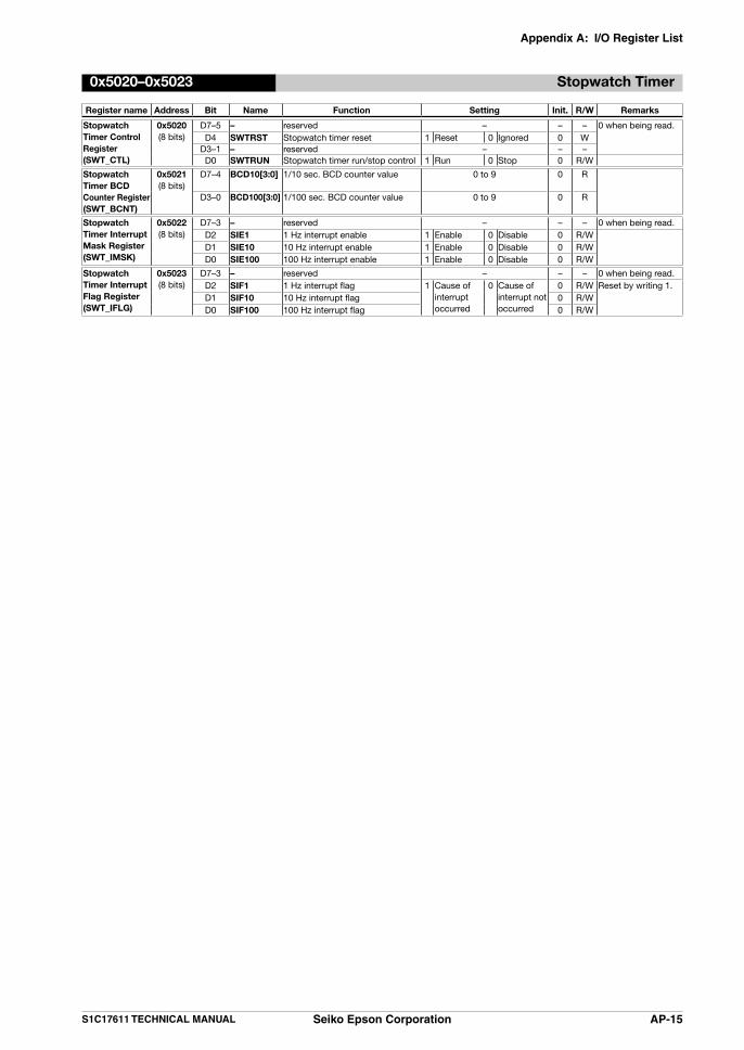
Appendix A: I/O Register List
S1C17611 TECHNICAL MANUAL Seiko Epson Corporation AP-15
0x5020–0x5023 Stopwatch Timer
Register name Address Bit Name Function Setting Init. R/W Remarks
Stopwatch Timer Control Register(SWT_CTL)
0x5020(8 bits)
D7–5 – reserved – – – 0 when being read.D4 SWTRST Stopwatch timer reset 1 Reset 0 Ignored 0 W
D3–1 – reserved – – –D0 SWTRUN Stopwatch timer run/stop control 1 Run 0 Stop 0 R/W
Stopwatch Timer BCD Counter Register(SWT_BCNT)
0x5021(8 bits)
D7–4
BCD10[3:0] 1/10 sec. BCD counter value 0 to 9 0 R
D3–0
BCD100[3:0] 1/100 sec. BCD counter value 0 to 9 0 R
Stopwatch Timer Interrupt Mask Register(SWT_IMSK)
0x5022(8 bits)
D7–3 – reserved – – – 0 when being read.D2 SIE1 1 Hz interrupt enable 1 Enable 0 Disable 0 R/WD1 SIE10 10 Hz interrupt enable 1 Enable 0 Disable 0 R/WD0 SIE100 100 Hz interrupt enable 1 Enable 0 Disable 0 R/W
Stopwatch Timer Interrupt Flag Register(SWT_IFLG)
0x5023(8 bits)
D7–3 – reserved – – – 0 when being read.D2 SIF1 1 Hz interrupt flag 1 Cause of
interrupt occurred
0 Cause of interrupt not occurred
0 R/W Reset by writing 1.D1 SIF10 10 Hz interrupt flag 0 R/WD0 SIF100 100 Hz interrupt flag 0 R/W

Appendix A: I/O Register List
AP-16 Seiko Epson Corporation S1C17611 TECHNICAL MANUAL
0x5040–0x5041 Watchdog Timer
Register name Address Bit Name Function Setting Init. R/W Remarks
Watchdog Timer Control Register(WDT_CTL)
0x5040(8 bits)
D7–5 – reserved – – – 0 when being read.D4 WDTRST Watchdog timer reset 1 Reset 0 Ignored 0 W
D3–0 WDTRUN [3:0]
Watchdog timer run/stop control
Other than 1010Run
1010Stop
1010 R/W
Watchdog Timer Status Register(WDT_ST)
0x5041(8 bits)
D7–2 – reserved – – – 0 when being read.
D1 WDTMD NMI/Reset mode select 1 Reset 0 NMI 0 R/WD0 WDTST NMI status 1 NMI occurred 0 Not occurred 0 R
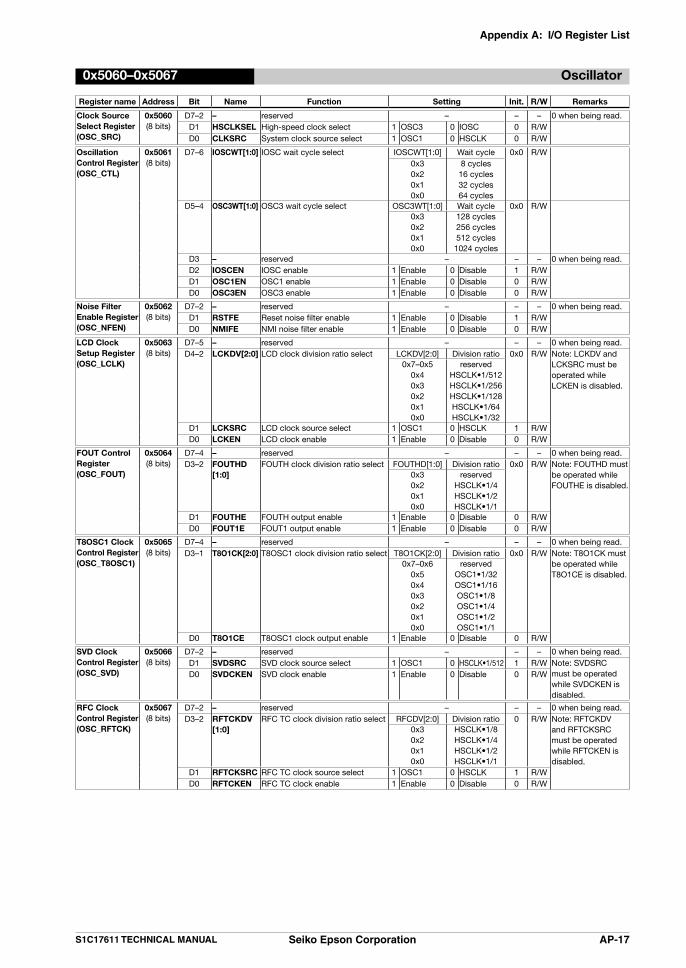
Appendix A: I/O Register List
S1C17611 TECHNICAL MANUAL Seiko Epson Corporation AP-17
0x5060–0x5067 Oscillator
Register name Address Bit Name Function Setting Init. R/W Remarks
Clock Source Select Register(OSC_SRC)
0x5060(8 bits)
D7–2 – reserved – – – 0 when being read.D1 HSCLKSEL High-speed clock select 1 OSC3 0 IOSC 0 R/WD0 CLKSRC System clock source select 1 OSC1 0 HSCLK 0 R/W
Oscillation Control Register(OSC_CTL)
0x5061(8 bits)
D7–6 IOSCWT[1:0] IOSC wait cycle select IOSCWT[1:0] Wait cycle 0x0 R/W0x30x20x10x0
8 cycles16 cycles32 cycles64 cycles
D5–4 OSC3WT[1:0] OSC3 wait cycle select OSC3WT[1:0] Wait cycle 0x0 R/W0x30x20x10x0
128 cycles256 cycles512 cycles
1024 cyclesD3 – reserved – – – 0 when being read.D2 IOSCEN IOSC enable 1 Enable 0 Disable 1 R/WD1 OSC1EN OSC1 enable 1 Enable 0 Disable 0 R/WD0 OSC3EN OSC3 enable 1 Enable 0 Disable 0 R/W
Noise Filter Enable Register(OSC_NFEN)
0x5062(8 bits)
D7–2 – reserved – – – 0 when being read.D1 RSTFE Reset noise filter enable 1 Enable 0 Disable 1 R/WD0 NMIFE NMI noise filter enable 1 Enable 0 Disable 0 R/W
LCD Clock Setup Register(OSC_LCLK)
0x5063(8 bits)
D7–5 – reserved – – – 0 when being read.D4–2 LCKDV[2:0] LCD clock division ratio select LCKDV[2:0] Division ratio 0x0 R/W Note: LCKDV and
LCKSRC must be operated while LCKEN is disabled.
0x7–0x50x40x30x20x10x0
reservedHSCLK•1/512HSCLK•1/256HSCLK•1/128HSCLK•1/64HSCLK•1/32
D1 LCKSRC LCD clock source select 1 OSC1 0 HSCLK 1 R/WD0 LCKEN LCD clock enable 1 Enable 0 Disable 0 R/W
FOUT Control Register(OSC_FOUT)
0x5064(8 bits)
D7–4 – reserved – – – 0 when being read.D3–2 FOUTHD
[1:0]FOUTH clock division ratio select FOUTHD[1:0] Division ratio 0x0 R/W Note: FOUTHD must
be operated while FOUTHE is disabled.
0x30x20x10x0
reservedHSCLK•1/4HSCLK•1/2HSCLK•1/1
D1 FOUTHE FOUTH output enable 1 Enable 0 Disable 0 R/WD0 FOUT1E FOUT1 output enable 1 Enable 0 Disable 0 R/W
T8OSC1 Clock Control Register(OSC_T8OSC1)
0x5065(8 bits)
D7–4 – reserved – – – 0 when being read.D3–1 T8O1CK[2:0] T8OSC1 clock division ratio select T8O1CK[2:0] Division ratio 0x0 R/W Note: T8O1CK must
be operated while T8O1CE is disabled.
0x7–0x60x50x40x30x20x10x0
reservedOSC1•1/32OSC1•1/16OSC1•1/8OSC1•1/4OSC1•1/2OSC1•1/1
D0 T8O1CE T8OSC1 clock output enable 1 Enable 0 Disable 0 R/W
SVD Clock Control Register(OSC_SVD)
0x5066(8 bits)
D7–2 – reserved – – – 0 when being read.D1 SVDSRC SVD clock source select 1 OSC1 0 HSCLK•1/512 1 R/W Note: SVDSRC
must be operated while SVDCKEN is disabled.
D0 SVDCKEN SVD clock enable 1 Enable 0 Disable 0 R/W
RFC Clock Control Register(OSC_RFTCK)
0x5067(8 bits)
D7–2 – reserved – – – 0 when being read.D3–2 RFTCKDV
[1:0]RFC TC clock division ratio select RFCDV[2:0] Division ratio 0 R/W Note: RFTCKDV
and RFTCKSRC must be operated while RFTCKEN is disabled.
0x30x20x10x0
HSCLK•1/8HSCLK•1/4HSCLK•1/2HSCLK•1/1
D1 RFTCKSRC RFC TC clock source select 1 OSC1 0 HSCLK 1 R/WD0 RFTCKEN RFC TC clock enable 1 Enable 0 Disable 0 R/W

Appendix A: I/O Register List
AP-18 Seiko Epson Corporation S1C17611 TECHNICAL MANUAL
0x5080–0x5081 Clock Generator
Register name Address Bit Name Function Setting Init. R/W Remarks
PCLK Control Register(CLG_PCLK)
0x5080(8 bits)
D7–2 – reserved – – – 0 when being read.D1–0 PCKEN[1:0] PCLK enable PCKEN[1:0] PCLK supply 0x3 R/W
0x30x20x10x0
EnableNot allowedNot allowed
Disable
CCLK Control Register(CLG_CCLK)
0x5081(8 bits)
D7–2 – reserved – – – 0 when being read.D1–0 CCLKGR[1:0] CCLK clock gear ratio select CCLKGR[1:0] Gear ratio 0x0 R/W
0x30x20x10x0
1/81/41/21/1
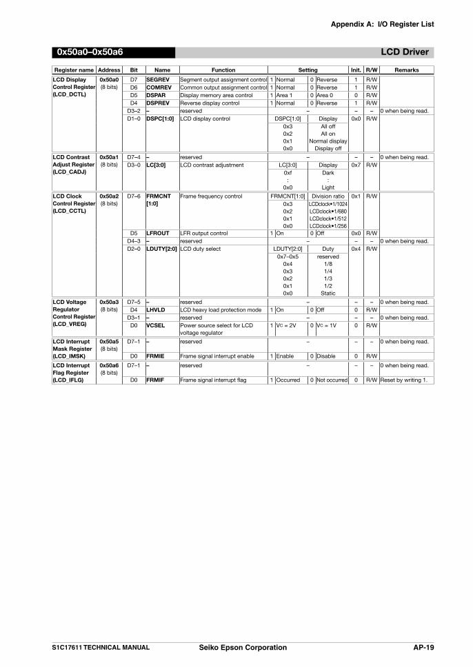
Appendix A: I/O Register List
S1C17611 TECHNICAL MANUAL Seiko Epson Corporation AP-19
0x50a0–0x50a6 LCD Driver
Register name Address Bit Name Function Setting Init. R/W Remarks
LCD Display Control Register(LCD_DCTL)
0x50a0(8 bits)
D7 SEGREV Segment output assignment control 1 Normal 0 Reverse 1 R/WD6 COMREV Common output assignment control 1 Normal 0 Reverse 1 R/WD5 DSPAR Display memory area control 1 Area 1 0 Area 0 0 R/WD4 DSPREV Reverse display control 1 Normal 0 Reverse 1 R/W
D3–2 – reserved – – – 0 when being read.D1–0 DSPC[1:0] LCD display control DSPC[1:0] Display 0x0 R/W
0x30x20x10x0
All offAll on
Normal displayDisplay off
LCD Contrast Adjust Register(LCD_CADJ)
0x50a1(8 bits)
D7–4 – reserved – – – 0 when being read.D3–0 LC[3:0] LCD contrast adjustment LC[3:0] Display 0x7 R/W
0xf:
0x0
Dark:
Light
LCD ClockControl Register(LCD_CCTL)
0x50a2(8 bits)
D7–6 FRMCNT[1:0]
Frame frequency control FRMCNT[1:0] Division ratio 0x1 R/W0x30x20x10x0
LCDclock•1/1024LCDclock•1/680LCDclock•1/512LCDclock•1/256
D5 LFROUT LFR output control 1 On 0 Off 0x0 R/WD4–3 – reserved – – – 0 when being read.D2–0 LDUTY[2:0] LCD duty select LDUTY[2:0] Duty 0x4 R/W
0x7–0x50x40x30x20x10x0
reserved1/81/41/31/2
Static
LCD Voltage RegulatorControl Register(LCD_VREG)
0x50a3(8 bits)
D7–5 – reserved – – – 0 when being read.D4 LHVLD LCD heavy load protection mode 1 On 0 Off 0 R/W
D3–1 – reserved – – – 0 when being read.D0 VCSEL Power source select for LCD
voltage regulator1 VC = 2V 0 VC = 1V 0 R/W
LCD Interrupt Mask Register(LCD_IMSK)
0x50a5(8 bits)
D7–1
– reserved – – – 0 when being read.
D0 FRMIE Frame signal interrupt enable 1 Enable 0 Disable 0 R/W
LCD Interrupt Flag Register(LCD_IFLG)
0x50a6(8 bits)
D7–1
– reserved – – – 0 when being read.
D0 FRMIF Frame signal interrupt flag 1 Occurred 0 Not occurred 0 R/W Reset by writing 1.

Appendix A: I/O Register List
AP-20 Seiko Epson Corporation S1C17611 TECHNICAL MANUAL
0x50c0–0x50c5 8-bit OSC1 Timer
Register name Address Bit Name Function Setting Init. R/W Remarks
8-bit OSC1 Timer Control Register(T8OSC1_CTL)
0x50c0(8 bits)
D7–5 – reserved – – – 0 when being read.D4 T8ORST Timer reset 1 Reset 0 Ignored 0 W
D3–2 – reserved – – –D1 T8ORMD Count mode select 1 One shot 0 Repeat 0 R/WD0 T8ORUN Timer run/stop control 1 Run 0 Stop 0 R/W
8-bit OSC1 Timer Counter Data Register(T8OSC1_CNT)
0x50c1(8 bits)
D7–0 T8OCNT [7:0]
Timer counter dataT8OCNT7 = MSBT8OCNT0 = LSB
0x0 to 0xff 0x0 R
8-bit OSC1 Timer Compare Data Register(T8OSC1_CMP)
0x50c2(8 bits)
D7–0 T8OCMP [7:0]
Compare dataT8OCMP7 = MSBT8OCMP0 = LSB
0x0 to 0xff 0x0 R/W
8-bit OSC1 Timer Interrupt Mask Register(T8OSC1_IMSK)
0x50c3(8 bits)
D7–1 – reserved – – – 0 when being read.D0 T8OIE 8-bit OSC1 timer interrupt enable 1 Enable 0 Disable 0 R/W
8-bit OSC1 Timer Interrupt Flag Register(T8OSC1_IFLG)
0x50c4(8 bits)
D7–1 – reserved – – – 0 when being read.D0 T8OIF 8-bit OSC1 timer interrupt flag 1 Cause of
interrupt occurred
0 Cause of interrupt not occurred
0 R/W Reset by writing 1.
8-bit OSC1 Timer PWM Duty Data Register(T8OSC1_DUTY)
0x50c5(8 bits)
D7–0 T8ODTY [7:0]
PWM output duty dataT8ODTY7 = MSBT8ODTY0 = LSB
0x0 to 0xff 0x0 R/W

Appendix A: I/O Register List
S1C17611 TECHNICAL MANUAL Seiko Epson Corporation AP-21
0x5100–0x5104 SVD Circuit
Register name Address Bit Name Function Setting Init. R/W Remarks
SVD Enable Register(SVD_EN)
0x5100(8 bits)
D7–1 – reserved – – – 0 when being read.D0 SVDEN SVD enable 1 Enable 0 Disable 0 R/W
SVD Compare Voltage Register(SVD_CMP)
0x5101(8 bits)
D7–4 – reserved – – – 0 when being read.D3–0 SVDC[3:0] SVD compare voltage SVDC[3:0] Voltage 0x0 R/W
0xf0xe0xd0xc0xb0xa0x90x80x70x60x50x40x30x20x10x0
3.2 V3.1 V3.0 V2.9 V2.8 V2.7 V2.6 V2.5 V2.4 V2.3 V2.2 V2.1 V2.0 V1.9 V1.8 V
reserved
SVD Detection Result Register(SVD_RSLT)
0x5102(8 bits)
D7–1 – reserved – – – 0 when being read.D0 SVDDT SVD detection result 1 Low 0 Normal × R
SVD Interrupt Mask Register(SVD_IMSK)
0x5103(8 bits)
D7–1 – reserved – – – 0 when being read.D0 SVDIE SVD interrupt enable 1 Enable 0 Disable 0 R/W
SVD Interrupt Flag Register(SVD_IFLG)
0x5104(8 bits)
D7–1 – reserved – – – 0 when being read.D0 SVDIF SVD interrupt flag 1 Cause of
interrupt occurred
0 Cause of interrupt not occurred
0 R/W Reset by writing 1.

Appendix A: I/O Register List
AP-22 Seiko Epson Corporation S1C17611 TECHNICAL MANUAL
0x5120 Power Generator
Register name Address Bit Name Function Setting Init. R/W Remarks
VD1 Control Register(VD1_CTL)
0x5120(8 bits)
D7–6 – reserved – – – 0 when being read.D5 HVLD VD1 heavy load protection mode 1 On 0 Off 0 R/WD4 – reserved – 0 R/W
D3–1 – reserved – – – 0 when being read.D0 VD1MD Flash erase/program mode 1 Flash (2.5 V) 0 Norm.(1.8 V) 0 R/W
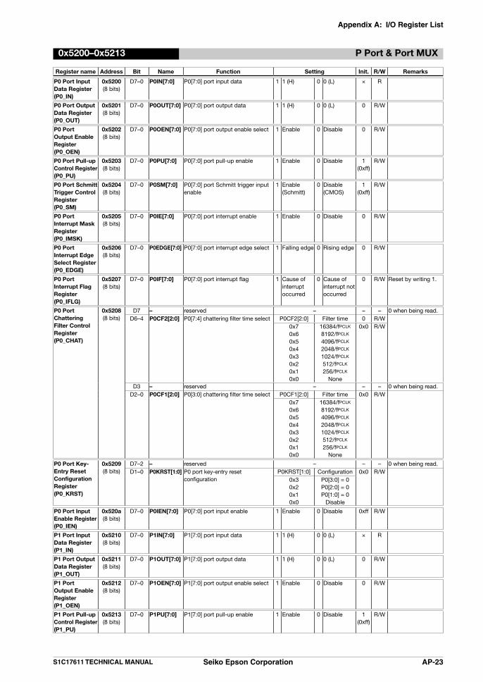
Appendix A: I/O Register List
S1C17611 TECHNICAL MANUAL Seiko Epson Corporation AP-23
0x5200–0x5213 P Port & Port MUX
Register name Address Bit Name Function Setting Init. R/W Remarks
P0 Port Input Data Register(P0_IN)
0x5200(8 bits)
D7–0 P0IN[7:0] P0[7:0] port input data 1 1 (H) 0 0 (L) × R
P0 Port Output Data Register(P0_OUT)
0x5201(8 bits)
D7–0 P0OUT[7:0] P0[7:0] port output data 1 1 (H) 0 0 (L) 0 R/W
P0 Port Output Enable Register(P0_OEN)
0x5202(8 bits)
D7–0 P0OEN[7:0] P0[7:0] port output enable select 1 Enable 0 Disable 0 R/W
P0 Port Pull-up Control Register(P0_PU)
0x5203(8 bits)
D7–0 P0PU[7:0] P0[7:0] port pull-up enable 1 Enable 0 Disable 1(0xff)
R/W
P0 Port Schmitt Trigger Control Register(P0_SM)
0x5204(8 bits)
D7–0 P0SM[7:0] P0[7:0] port Schmitt trigger input enable
1 Enable(Schmitt)
0 Disable(CMOS)
1(0xff)
R/W
P0 Port Interrupt Mask Register(P0_IMSK)
0x5205(8 bits)
D7–0 P0IE[7:0] P0[7:0] port interrupt enable 1 Enable 0 Disable 0 R/W
P0 Port Interrupt Edge Select Register(P0_EDGE)
0x5206(8 bits)
D7–0 P0EDGE[7:0] P0[7:0] port interrupt edge select 1 Falling edge 0 Rising edge 0 R/W
P0 Port Interrupt Flag Register(P0_IFLG)
0x5207(8 bits)
D7–0 P0IF[7:0] P0[7:0] port interrupt flag 1 Cause of interrupt occurred
0 Cause of interrupt not occurred
0 R/W Reset by writing 1.
P0 Port Chattering Filter Control Register(P0_CHAT)
0x5208(8 bits)
D7 – reserved – – – 0 when being read.D6–4 P0CF2[2:0] P0[7:4] chattering filter time select P0CF2[2:0] Filter time 0 R/W
0x70x60x50x40x30x20x10x0
16384/fPCLK
8192/fPCLK
4096/fPCLK
2048/fPCLK
1024/fPCLK
512/fPCLK
256/fPCLK
None
0x0 R/W
D3 – reserved – – – 0 when being read.D2–0 P0CF1[2:0] P0[3:0] chattering filter time select P0CF1[2:0] Filter time 0x0 R/W
0x70x60x50x40x30x20x10x0
16384/fPCLK
8192/fPCLK
4096/fPCLK
2048/fPCLK
1024/fPCLK
512/fPCLK
256/fPCLK
None
P0 Port Key-Entry Reset Configuration Register(P0_KRST)
0x5209(8 bits)
D7–2 – reserved – – – 0 when being read.D1–0 P0KRST[1:0] P0 port key-entry reset
configurationP0KRST[1:0] Configuration 0x0 R/W
0x30x20x10x0
P0[3:0] = 0P0[2:0] = 0P0[1:0] = 0
Disable
P0 Port Input Enable Register(P0_IEN)
0x520a(8 bits)
D7–0 P0IEN[7:0] P0[7:0] port input enable 1 Enable 0 Disable 0xff R/W
P1 Port Input Data Register(P1_IN)
0x5210(8 bits)
D7–0 P1IN[7:0] P1[7:0] port input data 1 1 (H) 0 0 (L) × R
P1 Port Output Data Register(P1_OUT)
0x5211(8 bits)
D7–0 P1OUT[7:0] P1[7:0] port output data 1 1 (H) 0 0 (L) 0 R/W
P1 Port Output Enable Register(P1_OEN)
0x5212(8 bits)
D7–0 P1OEN[7:0] P1[7:0] port output enable select 1 Enable 0 Disable 0 R/W
P1 Port Pull-up Control Register(P1_PU)
0x5213(8 bits)
D7–0 P1PU[7:0] P1[7:0] port pull-up enable 1 Enable 0 Disable 1(0xff)
R/W

Appendix A: I/O Register List
AP-24 Seiko Epson Corporation S1C17611 TECHNICAL MANUAL
0x5214–0x522a P Port & Port MUX
Register name Address Bit Name Function Setting Init. R/W Remarks
P1 Port Schmitt Trigger Control Register(P1_SM)
0x5214(8 bits)
D7–0 P1SM[7:0] P1[7:0] port Schmitt trigger input enable
1 Enable(Schmitt)
0 Disable(CMOS)
1(0xff)
R/W
P1 Port Interrupt Mask Register(P1_IMSK)
0x5215(8 bits)
D7–0 P1IE[7:0] P1[7:0] port interrupt enable 1 Enable 0 Disable 0 R/W
P1 Port Interrupt Edge Select Register(P1_EDGE)
0x5216(8 bits)
D7–0 P1EDGE[7:0] P1[7:0] port interrupt edge select 1 Falling edge 0 Rising edge 0 R/W
P1 Port Interrupt Flag Register(P1_IFLG)
0x5217(8 bits)
D7–0 P1IF[7:0] P1[7:0] port interrupt flag 1 Cause of interrupt occurred
0 Cause of interrupt not occurred
0 R/W Reset by writing 1.
P1 Port Chattering Filter Control Register(P1_CHAT)
0x5218(8 bits)
D7 – reserved – – – 0 when being read.D6–4 P1CF2[2:0] P1[7:4] chattering filter time P0CF2[2:0] Filter time 0 R/W
0x70x60x50x40x30x20x10x0
16384/fPCLK
8192/fPCLK
4096/fPCLK
2048/fPCLK
1024/fPCLK
512/fPCLK
256/fPCLK
None
0x0 R/W
D3 – reserved – – – 0 when being read.D2–0 P1CF1[2:0] P1[3:0] chattering filter time P0CF1[2:0] Filter time 0x0 R/W
0x70x60x50x40x30x20x10x0
16384/fPCLK
8192/fPCLK
4096/fPCLK
2048/fPCLK
1024/fPCLK
512/fPCLK
256/fPCLK
None
P1 Port Input Enable Register(P1_IEN)
0x521a(8 bits)
D7–0 P1IEN[7:0] P1[7:0] port input enable 1 Enable 0 Disable 0xff R/W
P2 Port Input Data Register(P2_IN)
0x5220(8 bits)
D7-3 – reserved – – – 0 when being read.D2–0 P2IN[2:0] P2[2:0] port input data 1 1 (H) 0 0 (L) × R
P2 Port Output Data Register(P2_OUT)
0x5221(8 bits)
D7-3 – reserved – – – 0 when being read.D2–0 P2OUT[2:0] P2[2:0] port output data 1 1 (H) 0 0 (L) 0 R/W
P2 Port Output Enable Register(P2_OEN)
0x5222(8 bits)
D7-3 – reserved – – – 0 when being read.D2–0 P2OEN[2:0] P2[2:0] port output enable select 1 Output
Enable0 Output
Disable0 R/W
P2 Port Pull-up Control Register(P2_PU)
0x5223(8 bits)
D7-3 – reserved – – – 1 when being read.D2–0 P2PU[2:0] P2[2:0] port pull-up enable 1 Enable 0 Disable 1
(0xff)R/W
P2 Port Schmitt Trigger Control Register(P2_SM)
0x5224(8 bits)
D7–3 – reserved – – – 1 when being read.D2–0 P2SM[2:0] P2[2:0] port Schmitt trigger input
enable1 Enable
(Schmitt)0 Disable
(CMOS)1
(0xff)R/W
P2 Port Input Enable Register(P2_IEN)
0x522a(8 bits)
D7-3 – reserved – – – 1 when being read.D2–0 P2IEN[2:0] P2[2:0] port input enable 1 Enable 0 Disable 0xff R/W

Appendix A: I/O Register List
S1C17611 TECHNICAL MANUAL Seiko Epson Corporation AP-25
0x52a0–0x52a2 P Port & Port MUX
Register name Address Bit Name Function Setting Init. R/W Remarks
P0 Port Function Select Register(P0_PMUX)
0x52a0(8 bits)
D7-6 P03MUX[1:0]
P03 port function select P03MUX[1:0] Port 0 R/W0x30x20x10x0
SCL1SCL0AIN3P03
D5-4 P02MUX[1:0]
P02 port function select P02MUX[1:0] Port 0 R/W0x30x20x10x0
reservedRFCLKOTOUT5
P02D3-2 P01MUX
[1:0]P01 port function select P01MUX[1:0] Port 0 R/W
0x30x20x10x0
reservedEXOSC3
OSC3P01
D1-0 P00MUX[1:0]
P00 port function select P00MUX[1:0] Port 0 R/W0x30x20x10x0
reservedFOUT1OSC4P00
P0 Port Function Select Register(P0_PMUX)
0x52a1(8 bits)
D7-6 P07MUX[1:0]
P07 port function select P07MUX[1:0] Port 0 R/W0x30x20x10x0
reservedFOUTH
RFINP07
D5-4 P06MUX[1:0]
P06 port function select P06MUX[1:0] Port 0 R/W0x30x20x10x0
LFROFOUT1AIN0P06
D3-2 P05MUX[1:0]
P05 port function select P05MUX[1:0] Port 0 R/W0x30x20x10x0
reservedTOUT4AIN1
P05/EXCL3 (T16E)
D1-0 P04MUX[1:0]
P04 port function select P04MUX[1:0] Port 0 R/W0x30x20x10x0
SDA1SDA0AIN2P04
P1 Port Function Select Register(P1_PMUX)
0x52a2(8 bits)
D7-6 P13MUX[1:0]
P13 port function select P13MUX[1:0] Port 0 R/W0x30x20x10x0
TOUTN3FOUTHSOUTP13
D5-4 P12MUX[1:0]
P12 port function select P12MUX[1:0] Port 0 R/W0x30x20x10x0
TOUT3SCLKSENBP12
D3-2 P11MUX[1:0]
P11 port function select P11MUX[1:0] Port 0 R/W0x30x20x10x0
reservedTOUT4SENAP11
D1-0 P10MUX[1:0]
P10 port function select P10MUX[1:0] Port 0 R/W0x30x20x10x0
reservedTOUTN4
REFP10

Appendix A: I/O Register List
AP-26 Seiko Epson Corporation S1C17611 TECHNICAL MANUAL
0x52a3–0x52a4 P Port & Port MUX
Register name Address Bit Name Function Setting Init. R/W Remarks
P1 Port Function Select Register(P1_PMUX)
0x52a3(8 bits)
D7 – reserved – – – 0 when being read.D6 P17MUX P17 port function select P17MUX[1:0] Port 0 R/W
0x10x0
SDOP17/EXCL1
D5 – reserved – – – 0 when being read.D4 P16MUX P16 port function select P16MUX[1:0] Port 0 R/W
0x10x0
SDIP16/EXCL2
D3-2 P15MUX[1:0]
P15 port function select P15MUX[1:0] Port 0 R/W0x30x20x10x0
TOUT3#BFR
#SPISSP15
D1-0 P14MUX[1:0]
P14 port function select P14MUX[1:0] Port 0 R/W0x30x20x10x0
reserved#ADTRG
SINP14/EXCL4
P2 Port Function Select Register(P2_PMUX)
0x52a4(8 bits)
D7 – reserved – – – 0 when being read.D6 P23MUX P23 port function select P23MUX[1:0] Port 0 R/W
0x10x0
reservedDCLK
D5 – reserved – – – 0 when being read.D4 P22MUX P22 port function select P22MUX[1:0] Port 0 R/W
0x10x0
P22DST2
D3 – reserved – – – 0 when being read.D2 P21MUX P21 port function select P21MUX[1:0] Port 0 R/W
0x10x0
P21DSIO
D1-0 P20MUX[1:0]
P20 port function select P20MUX[1:0] Port 0 R/W0x30x20x10x0
reservedTOUT5SPICLK
P20/EXCL0

Appendix A: I/O Register List
S1C17611 TECHNICAL MANUAL Seiko Epson Corporation AP-27
0x5300–0x530c PWM Timer Ch.0
Register name Address Bit Name Function Setting Init. R/W Remarks
PWM Timer Ch.0 Compare Data A Register(T16E_CA0)
0x5300(16 bits)
D15–0 T16ECA[15:0] Compare data AT16ECA15 = MSBT16ECA0 = LSB
0x0 to 0xffff 0x0 R/W
PWM Timer Ch.0 Compare Data B Register(T16E_CB0)
0x5302(16 bits)
D15–0 T16ECB[15:0] Compare data BT16ECB15 = MSBT16ECB0 = LSB
0x0 to 0xffff 0x0 R/W
PWM Timer Ch.0 Counter Data Register(T16E_TC0)
0x5304(16 bits)
D15–0 T16ETC[15:0] Counter dataT16ETC15 = MSBT16ETC0 = LSB
0x0 to 0xffff 0x0 R/W
PWM Timer Ch.0 Control Register(T16E_CTL0)
0x5306(16 bits)
D15–9 – reserved – – – 0 when being read.D8 INITOL Initial output level 1 High 0 Low 0 R/WD7 – reserved – – – 0 when being read.D6 SELFM Fine mode select 1 Fine mode 0 Normal mode 0 R/WD5 CBUFEN Comparison buffer enable 1 Enable 0 Disable 0 R/WD4 INVOUT Inverse output 1 Invert 0 Normal 0 R/WD3 CLKSEL Input clock select 1 External 0 Internal 0 R/WD2 OUTEN Clock output enable 1 Enable 0 Disable 0 R/WD1 T16ERST Timer reset 1 Reset 0 Ignored 0 W 0 when being read.D0 T16ERUN Timer run/stop control 1 Run 0 Stop 0 R/W
PWM Timer Ch.0 Input Clock Select Register(T16E_CLK0)
0x5308(16 bits)
D15–4 – reserved – – – 0 when being read.D3–0 T16EDF[3:0] Timer input clock select
(Prescaler output clock)T16EDF[3:0] Clock 0x0 R/W
0xf0xe0xd0xc0xb0xa0x90x80x70x60x50x40x30x20x10x0
reservedPCLK•1/16384PCLK•1/8192PCLK•1/4096PCLK•1/2048PCLK•1/1024PCLK•1/512PCLK•1/256PCLK•1/128PCLK•1/64PCLK•1/32PCLK•1/16PCLK•1/8PCLK•1/4PCLK•1/2PCLK•1/1
PWM Timer Ch.0 Interrupt Mask Register(T16E_IMSK0)
0x530a(16 bits)
D15–2 – reserved – – – 0 when being read.
D1 CBIE Compare B interrupt enable 1 Enable 0 Disable 0 R/WD0 CAIE Compare A interrupt enable 1 Enable 0 Disable 0 R/W
PWM Timer Ch.0 Interrupt Flag Register(T16E_IFLG0)
0x530c(16 bits)
D15–2 – reserved – – – 0 when being read.D1 CBIF Compare B interrupt flag 1 Cause of
interrupt occurred
0 Cause of interrupt not occurred
0 R/W Reset by writing 1.
D0 CAIF Compare A interrupt flag 0 R/W
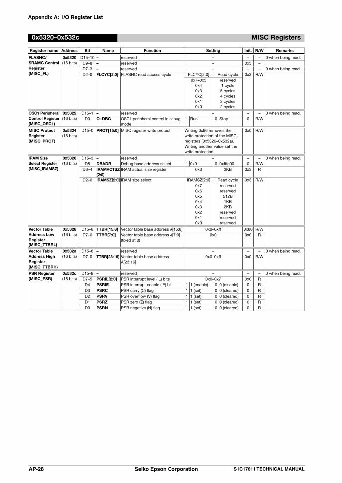
Appendix A: I/O Register List
AP-28 Seiko Epson Corporation S1C17611 TECHNICAL MANUAL
0x5320–0x532c MISC Registers
Register name Address Bit Name Function Setting Init. R/W Remarks
FLASHC/SRAMC Control Register(MISC_FL)
0x5320(16 bits)
D15–10 – reserved – – – 0 when being read.D9–8 – reserved – 0x3 –D7–3 – reserved – – – 0 when being read.D2–0 FLCYC[2:0] FLASHC read access cycle FLCYC[2:0] Read cycle 0x3 R/W
0x7–0x50x40x30x20x10x0
reserved1 cycle5 cycles4 cycles3 cycles2 cycles
OSC1 Peripheral Control Register(MISC_OSC1)
0x5322(16 bits)
D15–1 – reserved – – – 0 when being read.D0 O1DBG OSC1 peripheral control in debug
mode1 Run 0 Stop 0 R/W
MISC Protect Register(MISC_PROT)
0x5324(16 bits)
D15–0 PROT[15:0] MISC register write protect Writing 0x96 removes the write protection of the MISC registers (0x5326–0x532a).Writing another value set the write protection.
0x0 R/W
IRAM Size Select Register(MISC_IRAMSZ)
0x5326(16 bits)
D15–3 – reserved – – – 0 when being read.D8 DBADR Debug base address select 1 0x0 0 0xfffc00 0 R/W
D6–4 IRAMACTSZ[2:0]
IRAM actual size register 0x3 2KB 0x3 R
D2–0 IRAMSZ[2:0] IRAM size select IRAMSZ[2:0] Read cycle 0x3 R/W0x70x60x50x40x30x20x10x0
reservedreserved
512B1KB2KB
reservedreservedreserved
Vector Table Address Low Register(MISC_TTBRL)
0x5328(16 bits)
D15–8 TTBR[15:8] Vector table base address A[15:8] 0x0–0xff 0x80 R/WD7–0 TTBR[7:0] Vector table base address A[7:0]
(fixed at 0)0x0 0x0 R
Vector Table Address High Register (MISC_TTBRH)
0x532a(16 bits)
D15–8 – reserved – – – 0 when being read.D7–0 TTBR[23:16] Vector table base address
A[23:16]0x0–0xff 0x0 R/W
PSR Register(MISC_PSR)
0x532c(16 bits)
D15–8 – reserved – – – 0 when being read.D7–5 PSRIL[2:0] PSR interrupt level (IL) bits 0x0–0x7 0x0 RD4 PSRIE PSR interrupt enable (IE) bit 1 1 (enable) 0 0 (disable) 0 RD3 PSRC PSR carry (C) flag 1 1 (set) 0 0 (cleared) 0 RD2 PSRV PSR overflow (V) flag 1 1 (set) 0 0 (cleared) 0 RD1 PSRZ PSR zero (Z) flag 1 1 (set) 0 0 (cleared) 0 RD0 PSRN PSR negative (N) flag 1 1 (set) 0 0 (cleared) 0 R

Appendix A: I/O Register List
S1C17611 TECHNICAL MANUAL Seiko Epson Corporation AP-29
0x5360–0x536c PWM Timer Ch.1
Register name Address Bit Name Function Setting Init. R/W Remarks
PWM Timer Ch.1 Compare Data A Register(T16E_CA1)
0x5360(16 bits)
D15–0 T16ECA[15:0] Compare data AT16ECA15 = MSBT16ECA0 = LSB
0x0 to 0xffff 0x0 R/W
PWM Timer Ch.1 Compare Data B Register(T16E_CB1)
0x5362(16 bits)
D15–0 T16ECB[15:0] Compare data BT16ECB15 = MSBT16ECB0 = LSB
0x0 to 0xffff 0x0 R/W
PWM Timer Ch.1 Counter Data Register(T16E_TC1)
0x5364(16 bits)
D15–0 T16ETC[15:0] Counter dataT16ETC15 = MSBT16ETC0 = LSB
0x0 to 0xffff 0x0 R/W
PWM Timer Ch.1 Control Register(T16E_CTL1)
0x5366(16 bits)
D15–7 – reserved – – – 0 when being read.D8 INITOL Initial output level 1 High 0 Low 0 R/WD7 – reserved – – – 0 when being read.D6 SELFM Fine mode select 1 Fine mode 0 Normal mode 0 R/WD5 CBUFEN Comparison buffer enable 1 Enable 0 Disable 0 R/WD4 INVOUT Inverse output 1 Invert 0 Normal 0 R/WD3 CLKSEL Input clock select 1 External 0 Internal 0 R/WD2 OUTEN Clock output enable 1 Enable 0 Disable 0 R/WD1 T16ERST Timer reset 1 Reset 0 Ignored 0 W 0 when being read.D0 T16ERUN Timer run/stop control 1 Run 0 Stop 0 R/W
PWM Timer Ch.1 Input Clock Select Register(T16E_CLK1)
0x5368(16 bits)
D15–4 – reserved – – – 0 when being read.D3–0 T16EDF[3:0] Timer input clock select
(Prescaler output clock)T16EDF[3:0] Clock 0x0 R/W
0xf0xe0xd0xc0xb0xa0x90x80x70x60x50x40x30x20x10x0
reservedPCLK•1/16384PCLK•1/8192PCLK•1/4096PCLK•1/2048PCLK•1/1024PCLK•1/512PCLK•1/256PCLK•1/128PCLK•1/64PCLK•1/32PCLK•1/16PCLK•1/8PCLK•1/4PCLK•1/2PCLK•1/1
PWM Timer Ch.1 Interrupt Mask Register(T16E_IMSK1)
0x536a(16 bits)
D15–2 – reserved – – – 0 when being read.
D1 CBIE Compare B interrupt enable 1 Enable 0 Disable 0 R/WD0 CAIE Compare A interrupt enable 1 Enable 0 Disable 0 R/W
PWM Timer Ch.1 Interrupt Flag Register(T16E_IFLG1)
0x536c(16 bits)
D15–2 – reserved – – – 0 when being read.D1 CBIF Compare B interrupt flag 1 Cause of
interrupt occurred
0 Cause of interrupt not occurred
0 R/W Reset by writing 1.
D0 CAIF Compare A interrupt flag 0 R/W

Appendix A: I/O Register List
AP-30 Seiko Epson Corporation S1C17611 TECHNICAL MANUAL
0x5380–0x5386 ADC10SA
Register name Address Bit Name Function Setting Init. R/W Remarks
A/D ConversionResult Register(ADC10_ADD)
0x5380(16 bits)
D15–0 ADD[15:0] A/D converted data@STMD=0ADD[15:10]=0,ADD9=MSB, ADD0=LSB@STMD=1ADD15=MSB,ADD6=LSB, ADD[5:0]=0
0-1023 0 R
A/D Trigger/Channel Select(ADC10_TRG)
0x5382(16 bits)
D15–14 – reserved – – – 0 when being read.D13–11 ADCE[2:0] End channel selection 0x0-0x7 0 R/WD10–8 ADCS[2:0] Start channel selection 0x0-0x7 0 R/W
D7 STMD Converted data store mode 1 AD[9:0], 6’b0
0 6’b0, AD[9:0]
0 R/W
D6 ADMS Conversion mode selection 1 continuous 0 Single 0 R/WD5–4 ADTS[1:0] Conversion trigger selection ADTS[1:0] trigger 0 R/W
0x30x20x10x0
#ADTRG pinreserved
16bit timersoftware
D3 – reserved – – – 0 when being read.D2–0 ADST[2:0] Sampling clock count ADST[2:0] count clock 0x7 R/W
0x70x60x50x40x30x20x10x0
9clocks8clocks7clocks6clocks5clocks4clocks3clocks2clocks
A/D Control/Status Register (ADC10_CTL)
0x5384(16 bits)
D15 – reserved – – – 0 when being read.D14–12 ADICH Internal conversion channel status 0x0-0x7 0 R
D11 – reserved – – – 0 when being read.D10 ADIBS Internal busy status 1 busy 0 idle 0 RD9 ADOWE Overwrite error flag 1 Error 0 Normal 0 R/W Reset by writing 1D8 ADCF Conversion-complete flag 1 Completed 0 Not
completed0 R Reset when ADADD
is read.D7–6 – reserved – – – 0 when being read.D5 ADOIE Overwrite interrupt enable 1 Enable 0 Disable 0 R/WD4 ADCIE Conversion-complete interrupt
enable1 Enable 0 Disable 0 R/W
D3–2 – reserved – – – 0 when being read.D1 ADCTL conversion control 1 Start/Run 0 Stop 0 R/W Stop by writing 0D0 ADEN A/D enable 1 Enable 0 Disable 0 R/W
A/D dividedFrequencyRegister(ADC_DIV)
0x5386(16 bits)
D15–4 – reserved – – – 0 when being read.D3–0 ADDF[3:0] A/D converter clock divided
frequency selectADDF[3:0] clock 0 R/W
0xf0xe0xd0xc0xb0xa0x90x80x70x60x50x40x30x20x10x0
reservedPCLK•1/32768PCLK•1/16384PCLK•1/8192PCLK•1/4096PCLK•1/2048PCLK•1/1024PCLK•1/512PCLK•1/256PCLK•1/128PCLK•1/64PCLK•1/32PCLK•1/16PCLK•1/8PCLK•1/4PCLK•1/2

Appendix A: I/O Register List
S1C17611 TECHNICAL MANUAL Seiko Epson Corporation AP-31
0x53a0–0x53ae RFC
Register name Address Bit Name Function Setting Init. R/W Remarks
RFC ControlRegister (RFC_CTL)
0x53a0(16 bits)
D15–8 – reserved – – – 0 when being read.D7 CONEN Continuous oscillation enable 1 Enable 0 Disable 0 R/WD6 EVTEN Event counter mode enable 1 Enable 0 Disable 0 R/W
D5–4 SMODE[1:0]
Sensor oscillation mode select0:Resistive sensor DC oscillation1:Resistive sensor AC oscillation2:Capacitive sensor DC oscillation
SMODE[1:0] mode 0 R/W0x30x20x10x0
reservedCDC modeRAC modeRDC mode
D3–1 – reserved – – – 0 when being read.D0 RFCEN RFC Enable 1 Enable 0 Disable 0 R/W
RFC Oscillation trigger (RFC_TRG)
0x53a2(16 bits)
D15–3 – reserved – – – 0 when being read.D2 SSENB Sensor B oscillation Start trigger 1 Read: Run
Write: Start0 Read: Run
Write: Start0 R/W *1*2*3*4
D1 SSENA Sensor A oscillation Start trigger 1 Read: RunWrite: Start
0 Read: RunWrite: Start
0 R/W *1*3*4
D0 SREF Reference dc oscillation Start trigger
1 Read: RunWrite: Start
0 Read: RunWrite: Start
0 R/W *1*3*4
RFC Measurement Counter LSB (RFC_MCL)
0x53a4(16 bits)
D15–0 MC[15:0] Measurement Counter data D15-0 0x0 to 0xffff 0 R/W
RFC Measurement Counter MSB (RFC_MCH)
0x53a6(16 bits)
D15–8 – reserved – – – 0 when being read.D7–0 MC[23:16] Measurement Counter data
D23-160x0 to 0xff 0 R/W
RFC Time BaseCounter LSB (RFC_TCL)
0x53a8(16 bits)
D15–0 TC[15:0] Time base Counter data D15-0 0x0 to 0xffff 0 R/W
RFC Time BaseCounter MSB (RFC_MCH)
0x53aa(16 bits)
D15–8 – reserved – – – 0 when being read.D7–0 TC[23:16] Time base Counter data D23-16 0x0 to 0xff 0 R/W
RFC Interrupt Mask Register (RFC_IMSK)
0x53ac(16 bits)
D15–5 – reserved – – – 0 when being read.D4 OVTCIE Time base Counter Over flow
error interrupt enable1 Enable 0 Disable 0 R/W
D3 OVMCIE Measurement Counter Over flow error interrupt enable
1 Enable 0 Disable 0 R/W
D2 ESENBIE Sensor B oscillation end interrupt Enable
1 Enable 0 Disable 0 R/W
D1 ESENAIE Sensor A oscillation end interrupt Enable
1 Enable 0 Disable 0 R/W
D0 EREFIE Reference oscillation end Interrupt Enable
1 Enable 0 Disable 0 R/W
RFC Interrupt Flag Register (RFC_IFLG)
0x53ae(16 bits)
D15–5 – reserved – – – 0 when being read.D4 OVTCIF Time base Counter Over flow
error interrupt flag1 Cause of
interrupt occurred
0 Cause of interrupt not occurred
0 R/W Reset by writing 1
D3 OVMCIF Measurement Counter Over flow error interrupt flag
1 Cause of interrupt occurred
0 Cause of interrupt not occurred
0 R/W Reset by writing 1
D2 ESENBIF Sensor B oscillation end interrupt flag
1 Cause of interrupt occurred
0 Cause of interrupt not occurred
0 R/W Reset by writing 1
D1 ESENAIF Sensor A oscillation end interrupt flag
1 Cause of interrupt occurred
0 Cause of interrupt not occurred
0 R/W Reset by writing 1
D0 EREFIF Reference oscillation end Interrupt flag
1 Cause of interrupt occurred
0 Cause of interrupt not occurred
0 R/W Reset by writing 1
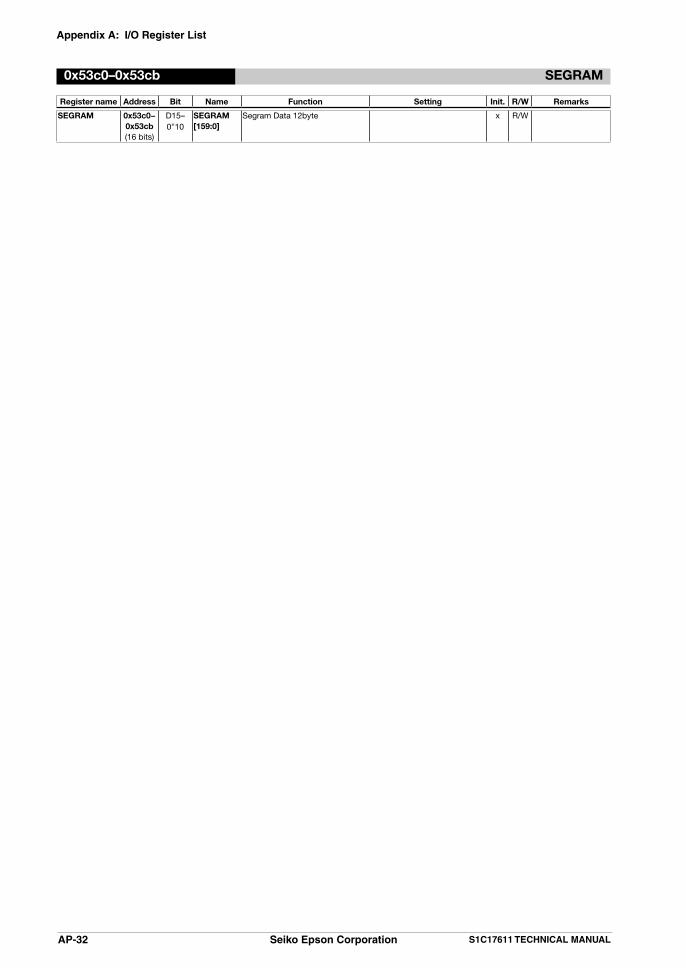
Appendix A: I/O Register List
AP-32 Seiko Epson Corporation S1C17611 TECHNICAL MANUAL
0x53c0–0x53cb SEGRAM
Register name Address Bit Name Function Setting Init. R/W Remarks
SEGRAM 0x53c0−0x53cb(16 bits)
D15–0*10
SEGRAM[159:0]
Segram Data 12byte x R/W
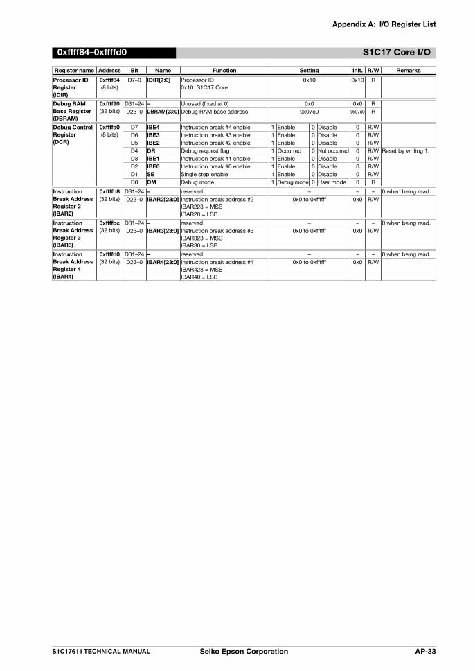
Appendix A: I/O Register List
S1C17611 TECHNICAL MANUAL Seiko Epson Corporation AP-33
0xffff84–0xffffd0 S1C17 Core I/O
Register name Address Bit Name Function Setting Init. R/W Remarks
Processor ID Register(IDIR)
0xffff84(8 bits)
D7–0 IDIR[7:0] Processor ID0x10: S1C17 Core
0x10 0x10 R
Debug RAM Base Register(DBRAM)
0xffff90(32 bits)
D31–24 – Unused (fixed at 0) 0x0 0x0 RD23–0 DBRAM[23:0] Debug RAM base address 0x07c0 0x07c0 R
Debug ControlRegister(DCR)
0xffffa0(8 bits)
D7 IBE4 Instruction break #4 enable 1 Enable 0 Disable 0 R/WD6 IBE3 Instruction break #3 enable 1 Enable 0 Disable 0 R/WD5 IBE2 Instruction break #2 enable 1 Enable 0 Disable 0 R/WD4 DR Debug request flag 1 Occurred 0 Not occurred 0 R/W Reset by writing 1.D3 IBE1 Instruction break #1 enable 1 Enable 0 Disable 0 R/WD2 IBE0 Instruction break #0 enable 1 Enable 0 Disable 0 R/WD1 SE Single step enable 1 Enable 0 Disable 0 R/WD0 DM Debug mode 1 Debug mode 0 User mode 0 R
InstructionBreak AddressRegister 2(IBAR2)
0xffffb8(32 bits)
D31–24 – reserved – – – 0 when being read.D23–0 IBAR2[23:0] Instruction break address #2
IBAR223 = MSBIBAR20 = LSB
0x0 to 0xffffff 0x0 R/W
InstructionBreak AddressRegister 3(IBAR3)
0xffffbc(32 bits)
D31–24 – reserved – – – 0 when being read.D23–0 IBAR3[23:0] Instruction break address #3
IBAR323 = MSBIBAR30 = LSB
0x0 to 0xffffff 0x0 R/W
InstructionBreak AddressRegister 4(IBAR4)
0xffffd0(32 bits)
D31–24 – reserved – – – 0 when being read.D23–0 IBAR4[23:0] Instruction break address #4
IBAR423 = MSBIBAR40 = LSB
0x0 to 0xffffff 0x0 R/W

Appendix B: Flash Memory Programming
AP-34 Seiko Epson Corporation S1C17611 TECHNICAL MANUAL
Appendix B: Flash Memory ProgrammingFlash memory programming consists of programming via a debugger using the flash writer function possessed by ICD (in-circuit debugger) such as the S5U1C17001H (ICD Mini) or self-programming via user programs.
B.1 Debugger ProgrammingThe debuggers included in the S1C17 Family C compiler packages provide functions that allow an ICD (e.g., S5U1C17001H) to be used as a flash writer.
USB cable(included with ICD package)
ICD (e.g., S5U1C17001H)
4-pin - 4-pintarget systemconnector cable(included with ICD package)
USB
Target board
Figure B.1.1: Flash memory programming system using debugger
To program S1C17611 flash memory using this function, you must install a 4-pin connector on the target board to connect the ICD (e.g., S5U1C17001H).Connect a 4-pin connector using the S1C17611 DCLK, DST2 (P22), and DSIO (P21) pins as debugging pins. (Note that this means P21 to P22 general input/output ports cannot be used.)
For more information on flash memory programming using this system, refer to the manual for the S1C17 Family C compiler package (e.g., S5U1C17001H). For more information on the 4-pin connector pin layout, refer to the ICD (e.g., S5U1C17001H) manual.

Appendix B: Flash Memory Programming
S1C17611 TECHNICAL MANUAL Seiko Epson Corporation AP-35
B.2 Self-programming via User ProgramsThe S1C17611 includes self-programming functions for erasing and overwriting flash memory by user programs executed while operating on the target board. A separately provided self-programming package provides function routines as object files for self-programming. Self-programming functions are easily added by linking these objects to user application programs. For more information, see the self-programming package manual.
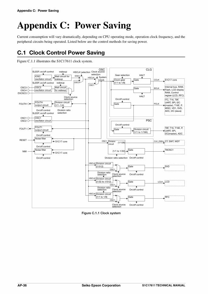
Appendix C: Power Saving
AP-36 Seiko Epson Corporation S1C17611 TECHNICAL MANUAL
Appendix C: Power SavingCurrent consumption will vary dramatically, depending on CPU operating mode, operation clock frequency, and the peripheral circuits being operated. Listed below are the control methods for saving power.
C.1 Clock Control Power SavingFigure C.1.1 illustrates the S1C17611 clock system.
HSCLKCCLK
OSC1
IOSC
OSC1
FOUTHoutput circuit
OSC1oscillator circuit
Division circuit(1/1~1/4)
Clock gear(1/1 to 1/8)
Gate S1C17 core
BCLK
CLK_256Hz
Gate
FOUTH
FOUT1output circuitFOUT1
Noise filterRESET
OSC1OSC2
HSCLK selection
Wait circuit for wakeup
wakeup
HALT
HALT
Division circuit(1/1 to 1/16K)
Noise filterNMI
CT, SWT, WDT
T8OSC1
Division circuit
(1/128)
(1/1 to 1/32)
Gate
Gate
CLG
PSC
OSC
PCLKGate
T8F, T16, T16E, P, UART, SPI, I2C(master), ADC
LCLK
OSC1
HSCLK
HSCLK
HSCLK
SVD
OSC1
LCD
OSC1
RFC
Division circuit(1/512)
Division circuit(1/32 to 1/512)
Division circuit(1/1 to 1/8)
Gate
Gate
Gate
Clock sourceselection
Clock source selection
Clock source selection
Clock source selection
Systemclock
Gear selection
S1C17 core
S1C17 core
Division ratioselection
Division ratioselection
Division ratioselection
Division ratio selection On/off control
SLEEP, on/off control
On/off control
On/off control
On/off control
On/off control
IOSCoscillator circuit
SLEEP, on/off control
On/off control
On/off control
On/off control
On/off control
On/off control
Internal bus, RAM,Flash, LCD display RAM, Control regiser (LCD, RFC)
ITC, T16, T8F, UART, SPI, I2C (master), T16E, P, MISC, VD1, SVD, ADC, I2C (slave)
OSC3
Wait circuit for wakeup
OSC3oscillator circuit
OSC3OSC4
EXOSC3
wakeupSLEEP, on/off control
Clock source selection
Figure C.1.1 Clock system

Appendix C: Power Saving
S1C17611 TECHNICAL MANUAL Seiko Epson Corporation AP-37
This section describes clock systems that can be controlled via software and power-saving control details. For more information on control registers and control methods, refer to the respective module sections.
System SLEEP (All clocks stopped)• Execute slp instruction Execute the slp instruction when the entire system can be stopped. The CPU switches to SLEEP mode and
the system clocks stop. This also stops all peripheral circuits using clocks. Starting up the CPU from SLEEP mode is therefore limited to startup using ports (described later).
System clocks• Clock source selection (OSC module) Select between IOSC/OSC3 and OSC1 for the system clock source. Reduce current consumption by selecting
the OSC1 clock when low-speed processing is possible.
• IOSC/OSC3 oscillation circuit stop (OSC module) Operate the oscillation circuit comprising the system clock source. Where possible, stop the other circuit. You
can reduce current consumption by using OSC1 as the system clock and stopping the IOSC/OSC3 oscillation circuit.
CPU clock (CCLK)• Execute the halt instruction Execute the halt instruction when program execution by the CPU is not required—for example, when only
the display is required or for interrupt standby. The CPU switches to HALT mode and suspends operations, but the peripheral circuits maintain the status in place at the time of the halt instruction, enabling use of peripheral circuits for timers and interrupts. You can reduce power consumption even further by suspending unnecessary peripheral circuits before executing the halt instruction. The CPU is started from HALT mode using the port or interrupts from the peripheral circuit operating in HALT mode.
• Low-speed clock gear selection (CLG module) The CLG module can reduce CPU clock speeds to between 1/1 and 1/8 of the system clock via the clock gear
settings. Reduce current consumption by operating the CPU at the minimum speed required for applications.
Peripheral clock (PCLK)• PCLK stop (CLG module) Stop the PCLK clock feed from the CLG to peripheral circuits if none of the following peripheral circuits is
required.
Peripheral circuits operating with PCLK • Prescaler (PWM timer, remote controller, P port) • UART • 8-bit timer • 16-bit timer Ch.0 to Ch.2 • Interrupt controller • SPI • I2C (master/slave) • Power supply control circuit • P port and port MUX (control register, chattering filter) • PWM timer • MISC register • A/D converter • SVD circuit

Appendix C: Power Saving
AP-38 Seiko Epson Corporation S1C17611 TECHNICAL MANUAL
The peripheral modules listed below are operated by clocks other than PCLK, except for control register access.
This means PCLK is not required after the control register has been set and operation started.• Clock timer• Stopwatch timer• Watchdog timer• 8-bit OSC1 timer• LCD driver • R/F converter
Table C.1.1 shows a list of methods for clock control and starting/stopping the CPU.
Table C.1.1: Clock control listCurrent
consumptionOSC1 IOSC/OSC3 CPU (CCLK)
PCLK peripheral
OSC1 peripheral
CPU stop method
CPU startup method
LowStop Stop Stop Stop Stop
Execute slp instruction
1
Oscillation (system CLK)
Stop Stop Stop OperationExecute halt
instruction1, 2
Oscillation (system CLK)
Stop Stop Operation OperationExecute halt
instruction1, 2, 3
Oscillation(system CLK)
Stop Operation(1/1) Operation Operation
OscillationOscillation
(system CLK)Stop Operation Operation
Execute halt instruction
1, 2, 3
OscillationOscillation
(system CLK)Operation (Low gear)
Operation Operation
HighOscillation
Oscillation (system CLK)
Operation(1/1) Operation Operation
HALT and SLEEP mode cancellation methods (CPU startup method)
1. Startup by port Started up by input/output port interrupt and debug interrupt (ICD forced break).
2. Startup by OSC1 peripheral circuit Startup by LCD driver of OSC1 peripheral circuit Started up by clock timer, stopwatch timer, watchdog timer,
8-bit OSC1 timer, or LCD driver interrupts.
3. Startup by PCLK peripheral circuit Started up by PCLK peripheral circuit interrupt.

Appendix C: Power Saving
S1C17611 TECHNICAL MANUAL Seiko Epson Corporation AP-39
C.2 Reducing Power Consumption via Power Supply ControlThe available power supply controls are listed below.
Internal constant-voltage circuit• Setting the internal operating voltage VD1 to 2.5 V increases current consumption. For normal operations, set VD1 to 1.8 V, and switch to 2.5 V only for flash memory programming.
• Note that turning on internal constant-voltage circuit heavy load protection will increase current consumption. Turn off heavy load protection for normal operations. Turn on only if operations are unstable.
LCD constant-voltage circuit• Setting VCSEL = 0 , increases current consumption. When power voltage is more than 2.5 V, set VCSEL to 1.
• Turning on the LCD constant-voltage circuit heavy load protection will increase current consumption. Turn off heavy load protection for normal operations. Turn on only if the display is unstable.
• If no LCD display is being used, turn off the LCD driver.
Power supply voltage detection (SVD) circuit• Operating the SVD circuit will increase current consumption. Turn off power supply voltage detection unless it is required.

Appendix D: Mounting Precautions
AP-40 Seiko Epson Corporation S1C17611 TECHNICAL MANUAL
Appendix D: Mounting PrecautionsThis section describes various precautions for circuit board design and IC mounting.
Oscillator circuit• Oscillation characteristics depend on factors such as components used (oscillator, CG, CD) and circuit board
patterns. In particular, with ceramic or crystal oscillators, select the appropriate capacitors (CG, CD) only after fully evaluating components actually mounted on the circuit board.
• Oscillator clock disturbances caused by noise may cause malfunctions. To prevent such disturbances, consider the following points. The latest devices, in particular, are manufactured by microscopic processes, making them especially susceptible to noise.
Areas in which noise countermeasures are especially important include the OSC2 pin and related circuit components and wiring. OSC1 pin handling is equally important. The noise precautions required for the OSC1 and OSC2 pins are described below.
We also recommend applying similar noise countermeasures to high-speed oscillator circuits, such as the OSC3 and OSC4 pins and wiring.
(1) Components such as oscillators, resistors, and capacitors connected to the OSC1 (OSC3) and OSC2 (OSC4) pins should have the shortest connections possible.
(2) Wherever possible, avoid locating digital signal lines within 3 mm of the OSC1 (OSC3) and OSC2 (OSC4) pins or related circuit components and wiring. Rapidly-switching signals, in particular, should be kept at a distance from these components. Since the spacing between layers of multi-layer printed circuit boards is a mere 0.1 mm to 0.2 mm, the above precautions also apply when positioning digital signal lines on other layers.
Never place digital signal lines alongside such components or wiring, even if more than 3 mm distance or located on other layers. Avoid crossing wires.
(3) Use VSS to shield OSC1 (OSC3) and OSC2 (OSC4) pins and related wiring (including wiring for adjacent circuit board layers).
Layers wired should be adequately shielded as shown to the right. Fully ground adjacent layers, where possible. At minimum, shield the area at
least 5 mm around the above pins and wiring. Even after implementing these precautions, avoid configuring digital signal lines
in parallel, as described in (2) above. Avoid crossing even on discrete layers, except for lines carrying signals with low switching frequencies.
(4) After implementing these precautions, check the output clock waveform by running the actual application program within the product.
Use an oscilloscope to check outputs from the FOUT1 and FOUTH pins. You can check the quality of the OSC3 output waveform via the FOUTH output. Confirm that the
frequency is as designed, is free of noise, and has minimal jitter. You can check the quality of the OSC1 waveform via the FOUT1 output. In particular, enlarge the
areas before and after the clock rising and falling edges and take special care to confirm that the regions approximately 100 ns to either side are free of clock or spiking noise.
Failure to observe precautions (1) to (3) adequately may lead to jitter in the OSC3 output and noise in the OSC1 output. Jitter in the OSC3 output will reduce operating frequencies, while noise in the OSC1 output will destabilize timers operated by the OSC1 clock as well as CPU core operations when the system clock switches to OSC1.
OSC4
OSC3
VSS
VSS pattern example (OSC3)

Appendix D: Mounting Precautions
S1C17611 TECHNICAL MANUAL Seiko Epson Corporation AP-41
Reset circuit• The reset signal input to the #RESET pin when power is turned on will vary, depending on various factors,
such as power supply start-up time, components used, and circuit board patterns. Constants such as capacitance and resistance should be determined through thorough testing with real-world products. Account for resistance fluctuations when setting the #RESET pin pull-up resistance for constants settings.
• Components such as capacitors and resistors connected to the #RESET pin should have the shortest connections possible to prevent noise-induced resets.
Power supply circuit Sudden power supply fluctuations due to noise will cause malfunctions. Consider the following issues.
(1) Connections from the power supply to the VDD and VSS pins should be implemented via the shortest, thickest patterns possible.
(2) If a bypass capacitor is connected between VDD and VSS, connections between the VDD and VSS pins should be as short as possible.
VDD
VSS
Bypass capacitor connection example
VDD
VSS
Signal line location• To prevent electromagnetically-induced noise arising from mutual induction large-current signal lines should
not be positioned close to circuits susceptible to noise, such as oscillators.
• Locating signal lines in parallel over significant distances or crossing signal lines operating at high speed will cause malfunctions due to noise generated by mutual interference.
Specifically, avoid positioning crossing signal lines operating at high speed close to circuits susceptible to noise, such as oscillators.
OSC1, OSC3
OSC2, OSC4
VSS
Large-current signal lineHigh-speed operation signal line
Example of configuration to avoid

Appendix D: Mounting Precautions
AP-42 Seiko Epson Corporation S1C17611 TECHNICAL MANUAL
Noise-induced malfunctionsCheck the following three points if you suspect the presence of noise-induced IC malfunctions.
(1) DSIO pin Low-level noise to this pin will cause a switch to Debug mode. The switch to Debug mode can be
confirmed by the clock output from DCLK and a High signal from the DST2 pin. For the product version, we recommend connecting the DSIO pin directly to VDD or pulling up the DSIO
pin using a resistor not exceeding 10 kW. The IC includes an internal pull-up resistor. The resistor has a relatively high impedance of 100 kW to 500
kW and is not noise-resistant.
(2) #RESET pin Low-level noise to this pin will reset the IC. Depending on the input waveform, the reset may not proceed
correctly. This is more likely to occur if, due to circuit design choices, the impedance is high when the reset input is High.
(3) VDD and VSS power supply The IC will malfunction the instant noise falling below the rated voltage is input. Incorporate countermeasures on the circuit board, including close patterns for circuit board power supply
circuits, noise-filtering decoupling capacitors, and surge/noise prevention components on the power supply line.
Perform the inspections described above using an oscilloscope capable of observing waveforms of at least 200 MHz. It may not be possible to observe high-speed noise events with a low-speed oscilloscope.
If you detect potential noise-induced malfunctions while observing the waveform with an oscilloscope, recheck with a low-impedance (less than 1 kW) connecting the relevant pin to GND or to the power supply. Malfunctions at that pin are likely if changes are visible, such as the malfunction disappearing, becoming less frequent, or the phenomena changing.
The DSIO and #RESET input circuits described above detect input signal edges and are susceptible to malfunctions induced by spike noise. This makes these digital signal pins the most susceptible to noise.To reduce potential noise, keep the following two points in mind when designing circuit boards:
(A) It is important to use low impedance resistors when driving the signals, as described above. Avoid connecting impedance exceeding 1 kW (ideally, 0 W) to the power supply or GND. The signal lines connected should be no longer than approximately 5 cm.
(B) Signals switching from 1 to 0 or 0 to 1 may generate noise if signal lines run parallel to other digital lines on the circuit board.
The highest risk of noise occurs in configurations in which a line is sandwiched between multiple signal lines that vary in synchrony. You can minimize noise effects by reducing the length of parallel sections (limit to a few cm) or by increasing the separation (to at least 2 mm).

Appendix D: Mounting Precautions
S1C17611 TECHNICAL MANUAL Seiko Epson Corporation AP-43
Handling of light (for bare chip mounting) The characteristics of semiconductor components can vary when exposed to light. IC may malfunction or
nonvolatile memory data may be corrupted if IC is exposed to light. Consider the following precautions for circuit boards and products in which this IC is mounted to prevent IC
malfunctions attributable to light exposure.
(1) Design and mount the product so that the IC is shielded from light during use.
(2) Shield the IC from light during inspection processes.
(3) Shield the IC on the upper, underside, and side faces of the IC chip.
(4) Mount the IC chip within one week of opening the package. If the IC chip must be stored before mounting, take measures to ensure light shielding.
(5) Adequate evaluations are required to assess nonvolatile memory data retention characteristics before product delivery if the product is subjected to heat stress exceeding regular reflow conditions during mounting processes.
Miscellaneous This product series is manufactured using microscopic processes. Although it is designed to ensure basic IC reliability meeting EIAJ and MIL standards, consider the following
points when mounting the product. In addition to physical damage during mounting, minor variations over time may result in electrical damage
arising from disturbances in the form of voltages exceeding the absolute maximum rating. The following factors can give rise to these variations:
(1) Electromagnetically-induced noise from industrial power supplies used in mounting reflow, reworking after mounting, and individual characteristic evaluation (testing) processes;
(2) Electromagnetically-induced noise from a solder iron when soldering.
In particular, during soldering, take care to ensure that the soldering iron GND (tip potential) has the same potential as the IC GND.

Appendix E: Initialization Routine
AP-44 Seiko Epson Corporation S1C17611 TECHNICAL MANUAL
Appendix E: Initialization RoutineThis section lists typical vector tables and initialization routines.
boot.s.org 0x8000.section .rodata ...(1)
; ======================================================================; Vector table; ====================================================================== ; interrupt vector interrupt ; number offset source
.long BOOT ; 0x00 0x00 reset ...(2)
.long unalign_handler ; 0x01 0x04 unalign
.long nmi_handler ; 0x02 0x08 NMI
.long int03_handler ; 0x03 0x0c -
.long p0_handler ; 0x04 0x10 P0 port
.long p1_handler ; 0x05 0x14 P1 port
.long swt_handler ; 0x06 0x18 SWT
.long ct_handler ; 0x07 0x1c CT
.long t8osc1_handler ; 0x08 0x20 T8OSC1
.long svd_handler ; 0x09 0x24 SVD
.long lcd_handler ; 0x0a 0x28 LCD
.long t16e_0_handler ; 0x0b 0x2c T16E ch0
.long t8f_handler ; 0x0c 0x30 T8F
.long t16_0_handler ; 0x0d 0x34 T16 ch0
.long t16_1_handler ; 0x0e 0x38 T16 ch1
.long t16_2_handler ; 0x0f 0x3c T16 ch2
.long uart_0_handler ; 0x10 0x40 UART ch0
.long i2cs_handler ; 0x11 0x44 I2CS
.long spi_handler ; 0x12 0x48 SPI
.long i2c_handler ; 0x13 0x4c I2CM
.long t16e_1_handler ; 0x14 0x50 T16E ch1
.long int15_handler ; 0x15 0x54 -
.long adc_handler ; 0x16 0x58 ADC
.long rfc_handler ; 0x17 0x5c RFC
.long int18_handler ; 0x18 0x60 -
.long int19_handler ; 0x19 0x64 -
.long int1a_handler ; 0x1a 0x68 -
.long int1b_handler ; 0x1b 0x6c -
.long int1c_handler ; 0x1c 0x70 -
.long int1d_handler ; 0x1d 0x74 -
.long int1e_handler ; 0x1e 0x78 -
.long int1f_handler ; 0x1f 0x7c -
; ======================================================================; Program code; ======================================================================
.text ...(3)
.align 1
BOOT: ; ===== Initialize ===========================================
; ----- Stack pointer -------------------- Xld.a %sp, 0x07c0 ...(4)
; ----- Memory controller ---------------- Xld.a %r1, 0x5320 ; MISC register base address
; FLASHC Xld.a %r0, 0x04 ; 1 cycle access, under 8.2 MHz system clock ld.b [%r1], %r0 ; [0x5320] <= 0x04 ...(5)
; ===== Main routine ========================================= ...
Appendix E: Initialization Routine
S1C17611 TECHNICAL MANUAL Seiko Epson Corporation AP-45
; ======================================================================; Interrupt handler; ======================================================================
; ----- Address unalign --------------------------unalign_handler: ...
; ----- NMI -------------------------------------nmi_handler: ...
(1) .rodata section is declared to position vector table in .vector section.
(2) Interrupt processing routine address is defined as vector. intXX_handler can be used as software interrupt.
(3) Program code is written in .text section.
(4) Sets stack pointer.
(5) Sets the number of flash memory controller access cycles. 1 cycle access can be set if the system clock is 8.2 MHz or below. (See “3 Memory Map and Bus Control.”)

Appendix F: Recommended Oscillators
AP-46 Seiko Epson Corporation S1C17611 TECHNICAL MANUAL
Appendix F: Recommended OscillatorsEach optimum oscillator circuit constant varies depending on installation, applied voltage or other conditions. Evaluation by mounting oscillators on circuits should be requested from each oscillator manufacturer.
(1) OSC1 crystal oscillatorOscillation frequency(kHz) Manufacturer Model name
32.768 Epson Toyocom Corporation MC-146 (surface-mount type)32.768 Epson Toyocom Corporation C-002RX (lead type)
(2) OSC3 crystal oscillator
Oscillation frequency(MHz) Manufacturer Model name
4.0 Epson Toyocom Corporation MA-406 (surface-mount type)8.0 Epson Toyocom Corporation MA-406 (surface-mount type)
(3) OSC3 ceramic oscillator
Oscillation frequency(MHz) Manufacturer Model name
1.0 Murata Manufacturing CSBLA1M00J58-B0 (lead type)Murata Manufacturing CSBFB1M00J58-R1 (surface-mount type)
2.0 Murata Manufacturing CSTCC2M00G56-R0 (surface-mount type)4.0 Murata Manufacturing CSTLS4M00G56-B0 (lead type)
Murata Manufacturing CSTCR4M00G55-R0 (surface-mount type)8.0 Murata Manufacturing CSTLS8M00G56-B0 (lead type)
Murata Manufacturing CSTCE8M00G55-R0 (surface-mount type)
*Note: When CSBFB1M00J58-R1 or CSBLA1M00J58-B0 is used, mounting RD3 (6.8kW) is recommended.
*Note2: Evaluation of mounting oscillators on circuits should be requested on each oscillator manufacturer.
(4) Recommended value of CG3/CD3/RD3
Name frequency[Hz] Model number CG3 [pF] CD3 [pF] Rd [W]
X'tal3 4M MA-406(CL : 16pF) 27 27 08M MA-406(CL : 12pF) 18 18 0
Ceramic3 1M CSBFB1M00J58-R1 100 100 6.8kCSBLA1M00J58-B0 100 100 6.8k
2M CSTCC2M00G56-R0 (47) * (47) * 04M CSTCR4M00G55-R0 (39) * (39) * 0
CSTLS4M00G56-B0 (47) * (47) * 08M CSTCE8M00G55-R0 (33) * (33) * 0
CSTLS8M00G56-B0 (47) * (47) * 0
*( ) indicates the capacity included in oscillators.

REVISION HISTORY
Revision HistoryCode No. Page Contents
411882300 All New anactment411882301 4-4 Descriptions modified.
If the unstable operation occurs by programming operations as the below, Use the heavy load protection function....frequently, set the heavy load protection function to enable during these operations.
7-12, 7-13 Figure 7.10.2 and Figure 7.10.3 modified.10-7, 10-20, 10-28
Descriptions added. • An unexpected interrupt may occur after SLEEP status is canceled if the slp instruction is executed
while the chattering ...The chattering filter must be disabled before placing the CPU into SLEEP status.18-6 Descriptions modified.
(2)RDRY = 1, RD2B = 0...of the receive data buffer must be read out before an overrun error occurs.18-21 Descriptions modified.
RBFI bit in the UART_CTLx register Preventing transfer by setting RXEN to 0 clears (initializes) transfer data buffers. Before writing 0 to
RXEN, confirm the absence of data in the buffers awaiting transmission.19-3 Descriptions modified.
The Master mode SPI uses the internal clock output by the 16-bit timer Ch.1 as the SPI clock.Figure 19.3.1 modified. Figure 19.3.2 deleted.Description deleted. Since the internal circuit operates in sync with the PCLK clock, the input clock is used to synchronize
the differentiated PCLK clock.Descriptions modified. Note: The duty ratio of the clock input via the SPICLK pin must be 50%.
19-4, 19-5 Descriptions added. Note: When the SPI module is used in master...second and following bytes during continuous transfer.Figure 19.4.2 added.
19-6, 19-7 Figure 19.5.1 and Figure 19.5.2 deleted.Figure 19.5.1 added.
19-7 Descriptions modified. After a data transfer is completed ...guaranteed if SPEN is set to 0 while data is being sent or received.
19-8 Descriptions modified. If SPTBE is 0,→If SPTBE is 1,
19-11 Descriptions added. Note: Make sure that SPEN is set to 1 before...SPI_TXD register to start data transmission/reception.
20-3 Descriptions added. If the I2C master module communicates with a slave device which has clock stretching, Transfer rates
are limited up to 50 kbits/s in the Standard-mode, up to 200 kbits in the Fast-mode.20-6 Figure 20.5.2 modified.20-7 Descriptions modified.
The data is shifted into the shift register with the clock pulses, ....RXE is reset to 0 when D7 is loaded.20-8 Descriptions modified.
Before STP can be set to 1, confirm that TBUSY or RBUSY is reset to 0 from 1 (this indicates that the I2CM module has finished data transmit/receive...wait time is necessary before STP is set to 1.
Descriptions modified. Disabling data transfer ...the I2C bus is in busy status, the SCL0 and SDA0 output levels and transfer
data at that point cannot be guaranteed.20-9 Figure 20.5.6, Figure 20.5.7 and Figure 20.5.8 modified.20-10 Figure 20.5.9 modified.
Descriptions modified. Transmit buffer empty interrupt occurs when the data was only sent....NOTE: When I2CM interrupt
occurs, decide the transmit buffer empty interrupt or the receive buffer full interrupt by the program sequence of the I2C master. There’re not registers to decide which interrupt occurred.
20-13 Descriptions added. Setting the STP bit 1 makes the I2C master module...the 1/4 cycle of I2C clock, STP can set to 1.
21-1 Figure 21.1.1 modified.21-2 Descriptions modified.
I2C slave clock input/output pin...SCL line status and outputs low level to the I2C bus when clock stretch.21-4 Descriptions modified.
(one system clock (PCLK) cycle is required. Two PCLK cycles or more pulse width is recommended)Descriptions added. Note: When I2C slave module is slave transceiver mode,...depends on the PCLK frequency.
21-6 Descriptions modified. STOP condition detection clears BUSY. STOP or Repeated START condition detection clears SELECT-
ED.

REVISION HISTORY
21-7 Descriptions added. When the asynchronous address detection function is used, the data written before ASDET_EN is reset
in 0 becomes invalid. Therefore, the transmission data must be written, after TXEMP has been set to 1.21-8 Descriptions deleted.
1. Connecting the multiple slave devices to the I2C bus.21-10, 21-11 Figure 21.5.5, Figure 21.5.6, Figure 21.5.7 and Figure 21.5.8 modified.21-12 Descriptions modified.
7. DA_STOP: set to 1 if a STOP condition or a Repeated START condition is detected while this module is selected as the slave device
21-22 Descriptions modified. Indicates that a stop condition or a repeated start condition is detected...At the same time, it initializes
the I2C communication process.21-23 Descriptions modified.
After SELECTED is set to 1, it is reset to 0 when a STOP condition or a Repeated START condition is detected.
21-25 Descriptions deleted. 1. Connecting the multiple slave devices to the I2C bus.
23-1 Description deleted. • Sampling rate: 100kHz (Max.)
23-5 Descriptions modified. Configure fADCLK, ADST[2:0] so...Number of clock cycles set by ADST[2:0] + 11
23-16 Descriptions modified. When ADEN is 0, a trigger is not accepted.
29-1 Basic External Connection Diagram modified.

International Sales Operations
Document Code: 411882301First Issue January 2010
Revised April 2011 H
AMERICA
EPSON ELECTRONICS AMERICA, INC.2580 Orchard Parkway,San Jose, CA 95131, USAPhone: +1-800-228-3964 Fax: +1-408-922-0238
EUROPEEPSON EUROPE ELECTRONICS GmbHRiesstrasse 15, 80992 Munich,GERMANYPhone: +49-89-14005-0 Fax: +49-89-14005-110
ASIAEPSON (CHINA) CO., LTD.7F, Jinbao Bldg., No.89 Jinbao St., Dongcheng District,Beijing 100005, CHINAPhone: +86-10-8522-1199 Fax: +86-10-8522-1125
SHANGHAI BRANCH7F, Block B, Hi-Tech Bldg., 900 Yishan Road,Shanghai 200233, CHINAPhone: +86-21-5423-5577 Fax: +86-21-5423-4677
SHENZHEN BRANCH12F, Dawning Mansion, Keji South 12th Road,Hi-Tech Park, Shenzhen 518057, CHINAPhone: +86-755-2699-3828 Fax: +86-755-2699-3838
EPSON HONG KONG LTD.Unit 715-723, 7/F Trade Square, 681 Cheung Sha Wan Road,Kowloon, Hong Kong.Phone: +852-2585-4600 Fax: +852-2827-4346
EPSON TAIWAN TECHNOLOGY & TRADING LTD.14F, No. 7, Song Ren Road,Taipei 110, TAIWANPhone: +886-2-8786-6688 Fax: +886-2-8786-6660
EPSON SINGAPORE PTE., LTD.1 HarbourFront Place,#03-02 HarbourFront Tower One, Singapore 098633Phone: +65-6586-5500 Fax: +65-6271-3182
SEIKO EPSON CORP.KOREA OFFICE5F, KLI 63 Bldg., 60 Yoido-dong,Youngdeungpo-Ku, Seoul 150-763, KOREAPhone: +82-2-784-6027 Fax: +82-2-767-3677
SEIKO EPSON CORP.MICRODEVICES OPERATIONS DIVISION
Device Sales & Marketing Dept.421-8, Hino, Hino-shi, Tokyo 191-8501, JAPANPhone: +81-42-587-5814 Fax: +81-42-587-5117


