275
Atul Tiwari and Mark D. Soucek (eds.) Concise Encyclopedia of High Performance Silicones, (275–292) 2014 © Scrivener Publishing LLC
18Silicone-Based Soft Electronics
Shi Cheng1,* and Mikael Östling2
1Ericsson AB, Stockholm, Sweden, and KTH Royal Institute of Technology, Stockholm, Sweden2KTH Royal Institute of Technology, Stockholm, Sweden
AbstractLately, the marriage of elastic silicone rubbers and electronics has given birth to a radically new class of electronic devices and systems,
so-called silicone-based soft electronics. Based on this new concept, electronics can nowadays be built in soft , rubbery, biological for-
mats, for enabling numerous new applications, in which conventional rigid electronics are impossible to use.
Th is chapter briefl y reviews recent research advances in the emerging fi eld of soft electronics. Various strategies for realizing elastic
electronics are addressed, and the focus of this chapter lies in microfl uidic approaches. Recently reported elastomeric soft electronic
devices using microfl uidic techniques, e.g., elastic passive antennas, a soft RF radiation sensor, as well as a reversibly stretchable,
body-worn wireless strain sensor, are presented and analyzed in detail. Lastly, future perspectives and outlook for silicone-based soft
electronics are discussed.
Keywords: Antennas, elastomers, galinstan, integrated circuits (ICs), liquid alloy, microfl uidics, planar inverted cone antenna
(PICA), polydimethylsiloxane (PDMS), radiofrequency (RF), sensors, silicones, stretchable electronics, ultrawideband (UWB),
voltage-controlled oscillators (VCOs)
18.1 Introduction
Silicones, a category of polymers, are widely used in sealants,
adhesives, medical applications, and insulation, and can oft en
be made in “soft ” formats with fl exibility, foldability, and stretch-
ability. On the contrary, electronics represent a totally diff erent
fi eld, where devices are usually rigid, and retain static shapes
once fabricated. Th e overlapping between these two “soft ” and
“stiff ” worlds has not yet been seen until a few years ago.
Th e simple motivation to “soft en” conventional electronic
devices is that we as human beings are in soft , biological formats,
and wish to turn electronics into similar manner as our bodies.
Not only for enhanced user experience, but also for enabling a
broad spectrum of new applications. Reversible deformability,
transparency, and lightweight are desired features for future
electronics. Devices based on this new technology will be fold-
able, twistable, and stretchable into almost arbitrary curvilinear
shapes. Application examples may range from ultrathin, con-
formable health monitoring tapes that seamlessly attach to the
skin, “electronic/second skin,” to elastomeric medical implants
that are truly biocompatible to the tissues.
Exciting research on silicone-based soft electronics that
can withstand severe folding, twisting, and stressing, but
with maintained electronic functions, have been recently
pursued. Whitesides investigated mechanical characteristics
of gold thin fi lms on silicone rubber, polydimethylsiloxane
(PDMS) surfaces for the fi rst time in 1998 [1]. Wrinkled
electrodes on pre-strained elastomeric substrates were
subsequently employed to realize electroactive polymer
actuators [2]. Later, Wagner’s and Suo’s groups at Princeton
studied wrinkled gold electrodes on PDMS substrates [3, 4].
In-depth investigations on micromechanics as well as fur-
ther development of fabrication processes using relaxed and
pre-stretched PDMS substrates were also conducted. Rogers’
group at the University of Illinois, Urbana-Champaign,
has made the most impressive contribution to this emerg-
ing fi eld. Th eir core technology of foldable and stretchable
silicon integrated circuits (ICs) on “wavy” silicon ribbons
encased in elastomers opened up the possibilities of realiz-
ing soft electronic devices with a variety of new integrated
features and functions [5, 6]. A series of appealing devices
based on this concept, including hemispherical electronic
*Corresponding author: [email protected]

276 Concise Encyclopedia of High Performance Silicones
eye camera [7], stretchable solar modules [8], smart gloves/
skins [9], instrumented balloon catheters [10], and epi-
dermal electronic systems [11], and stretchable microscale
inorganic light-emitting diodes [12], were shown soon
aft erwards. An alternative approach utilizing anisotropic
etching of bulk wafers was also introduced by Rogers [13,
14]. Lately, meandered stretchable interconnects embedded
in thin silicone sheets for diff erent frequency ranges were
demonstrated [15–17]. New electrical nanocomposite mate-
rials consisting of sliver nanoparticles or carbon nanotubes/
grapheme exhibited promising electrical characteristics and
mechanical deformability as well [18, 19].
Initial research on silicone-based soft electronics involv-
ing microfl uidic methods was fi rst carried out by Whitesides
[20, 21]. Th is concept was subsequently extended to imple-
ment elastomeric direct current (DC) circuits, by injecting
eutectic gallium and indium alloy (EGaIn) into microfl uidic
channels in thin silicone rubber sheets [22–24]. All the pre-
viously mentioned studies, however, deal with either low
frequency ICs or relatively simple interconnects. Soft elec-
tronics operating at radio frequencies remained an unex-
ploited fi eld until early 2009, at which time Cheng reported
the fi rst stretchable fl uidic antennas for enabling wireless
communication and remote sensing [25, 26]. Similar work
using EGaIn alloy as conductors for the antennas instead
of Galinstan was presented soon aft er [27]. Signifi cantly
improved elasticity of the resulting antennas could be
achieved by introducing a diff erent type of siloxane [28], and
mechanically reconfi gurable antennas could also be realized
[29]. In 2010, Cheng proposed a heterogeneous integra-
tion strategy for the fi rst demonstration of active silicone-
based RF electronics, a fully integrated RF radiation sensor,
cf. Figure 18.1, [30]. A year later, further development on
this concept has been made to implement multilayer con-
fi gurations, and an elastomeric integrated large-area wireless
strain sensor was published, as seen in Figure 18.1 [31].
More details on emerging silicone-based soft eletronics
using microfl uidic approaches, are presented in the following
sections. Fabrication processes, intergration stragetries, as well
as application examples are addressed and discussed. Th e entire
chapter ends with concluding remarks and future perspectives.
18.2 Silicone-Based Passive Soft Electronics
Soft lithography, a well-known fabrication technique in the
microfl uidic society for constructing microstructured chan-
nels, is adapted to build soft electronics [32]. Microfl uidic
channels in soft electronic devices are fi lled with liquid metal
alloys other than chemical solutions or biological fl uids as in
conventional lab-on-chip microfl uidic devices.
18.2.1 Fabrication of Single-Layer Passive Elastomeric Electronics
Figure 18.2 illustrates the manufacturing process steps for
realizing silicone-based single-layer soft electronics. Master
construction, molding/casting, plasma/thermal bonding,
channel fi lling, as well as encapsulation are essential steps.
Using soft lithography techniques, all design patterns
are fi rst transferred to a SU-8 layer on top of a silicon wafer
from either plastic or glass masks. Th e thickness of the
SU-8 layer may vary from a few tenths of microns to sev-
eral hundred microns, depending on the design of electronic
devices. Development and thermal stabilization in order to
enhance the adhesion between SU-8 layer and silicon sub-
strate come as the second step. In the case of 100 μm thick
Figure 18.1 Silicone-based soft electronic devices: a) A reversibly
stretchable, body-worn wireless strain sensor. b) A microfl uidic,
soft RF radiation sensor.
Figure 18.2 Fabrication process of single-layer, silicone-rubber-
based passive soft electronics.
Silicone-Based Soft Electronics 277
SU-8 100 (MicroChem Newton, MA) layer, baking at 150°C
for 30 min is recommended. Subsequently, the mixture of
the PDMS prepolymer and crosslinker is poured onto the
structured SU-8 master, and then cured either at 70°C in an
oven for 30 min or at room temperature for 24 h. Th e fi n-
ished silicone rubber samples cured at the latter condition
oft en feature higher elasticity and fl exibility. A thin blank sil-
icone lid without the need for SU-8 masters can be prepared
in a similar way. Optional bonding techniques are plasma,
thermal, and uncured PDMS bonding. Liquid metal alloy,
e.g., Galinstan (68.5% Ga, 21.5% In, 10% Sn, σ=3.46⋅106
S/m) or EGaIn (75.5% Ga, 24.5% In, σ=3.40⋅106 S/m) can
be employed to fi ll microfl uidic channels inside the bonded
PDMS replica and blank lid. Th e entire fabrication process
ends with encapsulation of injection inlets and ventilation
outlets using uncured PDMS mixture. No special tempera-
ture requirements are needed for liquid metal alloy handling
since they remain at a liquid state at room temperature as
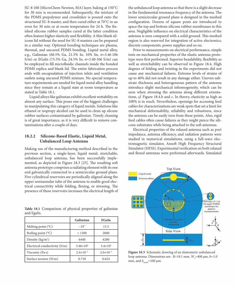
stated in Table 18.1.
Liquid alloys like galinstan exhibit excellent wettability on
almost any surface. Th is poses one of the biggest challenges
in manipulating this category of liquid metals. Solutions like
ethanol or isopropy alcohol can be used to clean up silcone
rubber surfaces contaminated by galinstan. Timely cleaning
is of great importance, as it is very diffi cult to remove con-
taminations aft er a couple of days.
18.2.2 Silicone-Based Elastic, Liquid Metal, Unbalanced Loop Antenna
Making use of the manufacturing method described in the
previous section, a single-layer, liquid metal, stretchable,
unbalanced loop antenna, has been successfully imple-
mented, as depicted in Figure 18.3 [25]. Th e resulting soft
antenna prototype comprises a radiating element with its one
end galvanically connected to a semicircular ground plane.
Five cylindrical reservoirs are periodically aligned along the
upper semiannular tube of the antenna to enable good elec-
trical connectivity while folding, fl exing, or stressing. Th e
presence of these reservoirs increases the electrical length of
the unbalanced loop antenna so that there is a slight decrease
in the fundamental resonance frequency of the antenna. Th e
lower semicircular ground plane is designed in the meshed
confi guration. Dozens of square posts are introduced to
space the top and bottom silicone rubber membranes in this
area. Negligible infl uence on electrical characteristics of the
antenna is seen compared with a solid ground. Th is meshed
region is also reserved for integration of active electronics,
discrete components, power supplies and so on.
Prior to measurements on electrical performance, simple
tests on mechanical properties of the elastic antenna proto-
type were fi rst performed. Superior bendability, fl exibility as
well as stretchability can be observed in Figure 18.4. High
degrees of folding and twisting in the experiments did not
cause any mechanical failures. Extreme levels of strains of
up to 40% did not result in any damage either. Uneven sub-
strate thickness and heterogeneous pattern of the antenna
introduce slight mechanical inhomogeneity, which can be
seen when stressing the antenna along diff erent orienta-
tions, cf. Figure 18.4.b and c. In theory, elasticity as high as
100% is in reach. Nevertheless, openings for accessing feed
cables for characterizations are weak spots that set a limit for
mechanical deformability, reliability and robustness, since
the antenna can be easily torn from these points. Also, rigid
feed cables oft en cause failures as they might pierce the sili-
cone substrates while being attached to the soft antennas.
Electrical properties of the relaxed antenna such as port
impedance, antenna effi ciency, and radiation patterns were
studied in numerical simulations, using a full-wave elec-
tromagnetic simulator, Ansoft High Frequency Structural
Simulator (HFSS). Experimental verifi cation on both relaxed
and fl exed antennas were performed aft erwards. Simulated
Table 18.1 Comparison of physical properties of galinstan and EgaIn.
Galinstan EGaIn
Melting point (°C) −19** 15.5
Boiling point (°C) > 1300 2000
Density (kg/m3) 6440 6280
Electrical conductivity (S/m) 3.46×10⁶ 3.4×10⁶
Viscosity (Pa·s) 2.4×10⁻³ 2.0×10⁻³
Surface tension (N/m) 0.718 0.624
Figure 18.3 Schematic drawing of an elastomeric unbalanced
loop antenna. Dimensions are: R=18.1 mm, WS=400 μm, h=1.0
mm, and hmetal
=100 μm.

278 Concise Encyclopedia of High Performance Silicones
and measured refl ection coeffi cients (S11
) are presented in
Figure 18.5. Th e non-strained antenna features good imped-
ance matching around 2.44 GHz, with an input impedance
of approximately 75+15j Ω. Strains applied on the antenna
lead to an increase in the length of the upper radiating loop
and result in a decreased resonance frequency, as seen in
Figure 18.5.b. Stressing the antenna along y-axis decreases its
input resistance due to the increased coupling between the
upper radiation arm and the lower ground plane, whereas
the resistance goes up when strains are applied along x-axis.
Numerical and experimental results on the antenna
radiation patterns at 2.44 GHz are shown in Figure 18.6.
Th e antenna in its relaxed state exhibits similar broad beam
coverage as conventional unbalanced loops, especially in
Figure 18.4 Photographs of the foldable, stretchable, fl uidic unbalanced loop antenna enclosed in a silicone substrate: a) in its relaxed state,
b) w/ 40% vertical strain, and c) horizontal elongation, d) in its folded state, e) w/ severe twisting, and f) biaxial stretching.
(a) (b)
Figure 18.5 Simulated and measured refl ection coeffi cients, S11
, of a silicone-based elastic unbalanced loop antenna. a) Simulated and
measured S11
(in logarithm scale) of the relaxed and fl exed antenna; b) Measured S11
of the fl exed antenna w/ 20% x-axis (solid), 40% x-axis
(dashed) and 20% y-axis (dotted), 40% y-axis (dashdot) strain. Th e S11
at 2.44 GHz is marked by a cross symbol on each curve.
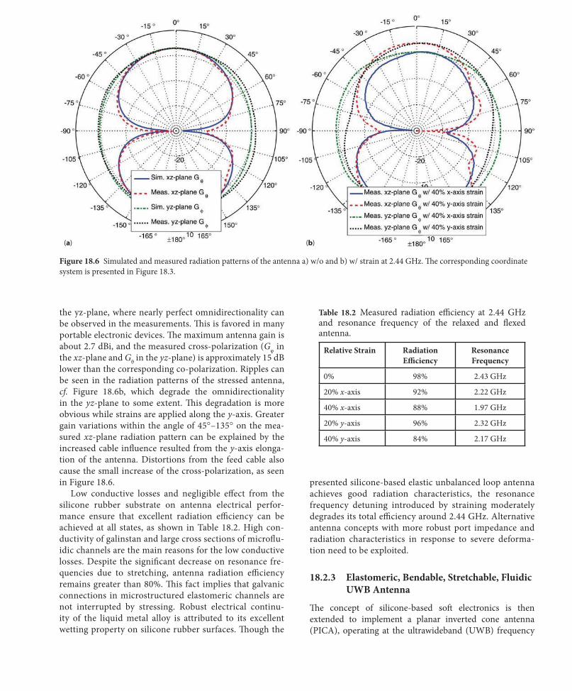
Silicone-Based Soft Electronics 279
the yz-plane, where nearly perfect omnidirectionality can
be observed in the measurements. Th is is favored in many
portable electronic devices. Th e maximum antenna gain is
about 2.7 dBi, and the measured cross-polarization (Gφ in
the xz-plane and Gθ in the yz-plane) is approximately 15 dB
lower than the corresponding co-polarization. Ripples can
be seen in the radiation patterns of the stressed antenna,
cf. Figure 18.6b, which degrade the omnidirectionality
in the yz-plane to some extent. Th is degradation is more
obvious while strains are applied along the y-axis. Greater
gain variations within the angle of 45°–135° on the mea-
sured xz-plane radiation pattern can be explained by the
increased cable infl uence resulted from the y-axis elonga-
tion of the antenna. Distortions from the feed cable also
cause the small increase of the cross-polarization, as seen
in Figure 18.6.
Low conductive losses and negligible eff ect from the
silicone rubber substrate on antenna electrical perfor-
mance ensure that excellent radiation effi ciency can be
achieved at all states, as shown in Table 18.2. High con-
ductivity of galinstan and large cross sections of microfl u-
idic channels are the main reasons for the low conductive
losses. Despite the signifi cant decrease on resonance fre-
quencies due to stretching, antenna radiation effi ciency
remains greater than 80%. Th is fact implies that galvanic
connections in microstructured elastomeric channels are
not interrupted by stressing. Robust electrical continu-
ity of the liquid metal alloy is attributed to its excellent
wetting property on silicone rubber surfaces. Th ough the
(a) (b)
Figure 18.6 Simulated and measured radiation patterns of the antenna a) w/o and b) w/ strain at 2.44 GHz. Th e corresponding coordinate
system is presented in Figure 18.3.
Table 18.2 Measured radiation effi ciency at 2.44 GHz and resonance frequency of the relaxed and fl exed antenna.
Relative Strain Radiation
Effi ciency
Resonance
Frequency
0% 98% 2.43 GHz
20% x-axis 92% 2.22 GHz
40% x-axis 88% 1.97 GHz
20% y-axis 96% 2.32 GHz
40% y-axis 84% 2.17 GHz
presented silicone-based elastic unbalanced loop antenna
achieves good radiation characteristics, the resonance
frequency detuning introduced by straining moderately
degrades its total effi ciency around 2.44 GHz. Alternative
antenna concepts with more robust port impedance and
radiation characteristics in response to severe deforma-
tion need to be exploited.
18.2.3 Elastomeric, Bendable, Stretchable, Fluidic UWB Antenna
Th e concept of silicone-based soft electronics is then
extended to implement a planar inverted cone antenna
(PICA), operating at the ultrawideband (UWB) frequency

280 Concise Encyclopedia of High Performance Silicones
range of 3.1–10.6 GHz [26]. Th e choice for such a wideband
antenna is that its electrical performance is expected to be
insensitive to mechanical deformation. Furthermore, its
ultrathin uniplanar confi guration makes it capable of toler-
ating extreme degrees of bending and stretching. Schematics
of the elastic PICA are depicted in Figure 18.7. Th e height
of the leaf-shaped radiator roughly corresponds to a quar-
ter wavelengths at the lowest resonance frequency of the
antenna, and the size of the ground plane has a minor eff ect
on electrical characteristics as long as it is suffi ciently large.
Th e gap between the radiating element and the ground
plane plays an essential role in antenna performance, and
determines the upper range of operational frequencies. Th e
smaller gaps lead to the higher frequencies. Th e two sym-
metrical tapered apertures formed by the inverted cone and
the ground plane act as a broadband impedance transformer
that gradually transfers the 50 Ω port impedance to the free
space impedance of approximately 377 Ω.
Resembling the soft unbalanced loop proposed previ-
ously, the soft PICA prototype features excellent revers-
ible foldability, fl exibility, and stretchability, as shown in
Figure 18.8. Extreme levels of straining of up to 40% along
either x- or y-axis do not cause any mechanical failures, cf.
Figure 18.7 Geometrical schematics of a 2D stretchable fl uid
metal PICA encapsulated in a silicone rubber substrate: R=10 mm,
Lg=25 mm, W
g=40 mm, G=300 μm, h=1 mm, and h
metal=100 μm.
Figure 18.8 Photographs of the resulting silicone-based highly fl exible, stretchable PICA prototype: a) in its relaxed state; w/ 40% strain
along its b) x- and c) y-axis; and d) w/ severe twisting. Th e corresponding coordinate system is shown in Figure 18.7.
Silicone-Based Soft Electronics 281
Figure 18.8b,c. Severe twisting and bending do not result in
any damages either. Aft er the removal of applied mechanical
forces, the antenna returns to its original state without any
visible deformation.
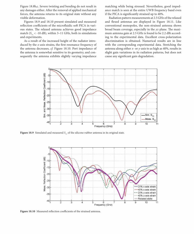
Figures 18.9 and 18.10 present simulated and measured
refl ection coeffi cients of the microfl uidic soft PICA in vari-
ous states. Th e relaxed antenna achieves good impedance
match (S11
< -10 dB), within 3–11 GHz, both in simulations
and experiments.
As a result of the increased height of the radiator intro-
duced by the x-axis strains, the fi rst resonance frequency of
the antenna decreases, cf. Figure 18.10. Port impedance of
the antenna is somewhat sensitive to its geometry, and con-
sequently the antenna exhibits slightly varying impedance
matching while being stressed. Nevertheless, good imped-
ance match is seen at the entire UWB frequency band even
if the PICA is signifi cantly strained up to 40%.
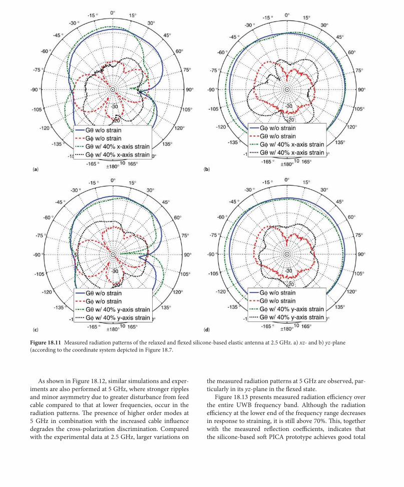
Radiation pattern measurements at 2.5 GHz of the relaxed
and fl exed antennas are displayed in Figure 18.11. Like
conventional monopoles, the non-strained antenna shows
broad beam coverage, especially in the yz-plane. Th e maxi-
mum antenna gain at 2.5 GHz is found to be 2.2 dBi accord-
ing to the experimental data. Excellent cross- polarization
discrimination is obtained. Numerical results are in line
with the corresponding experimental data. Stretching the
antenna along either x- or y-axis to as high as 40%, results in
slight gain variations in its radiation patterns, but does not
cause any signifi cant gain degradation.
Figure 18.9 Simulated and measured S11
of the silicone rubber antenna in its original state.
Figure 18.10 Measured refl ection coeffi cients of the strained antenna.
282 Concise Encyclopedia of High Performance Silicones
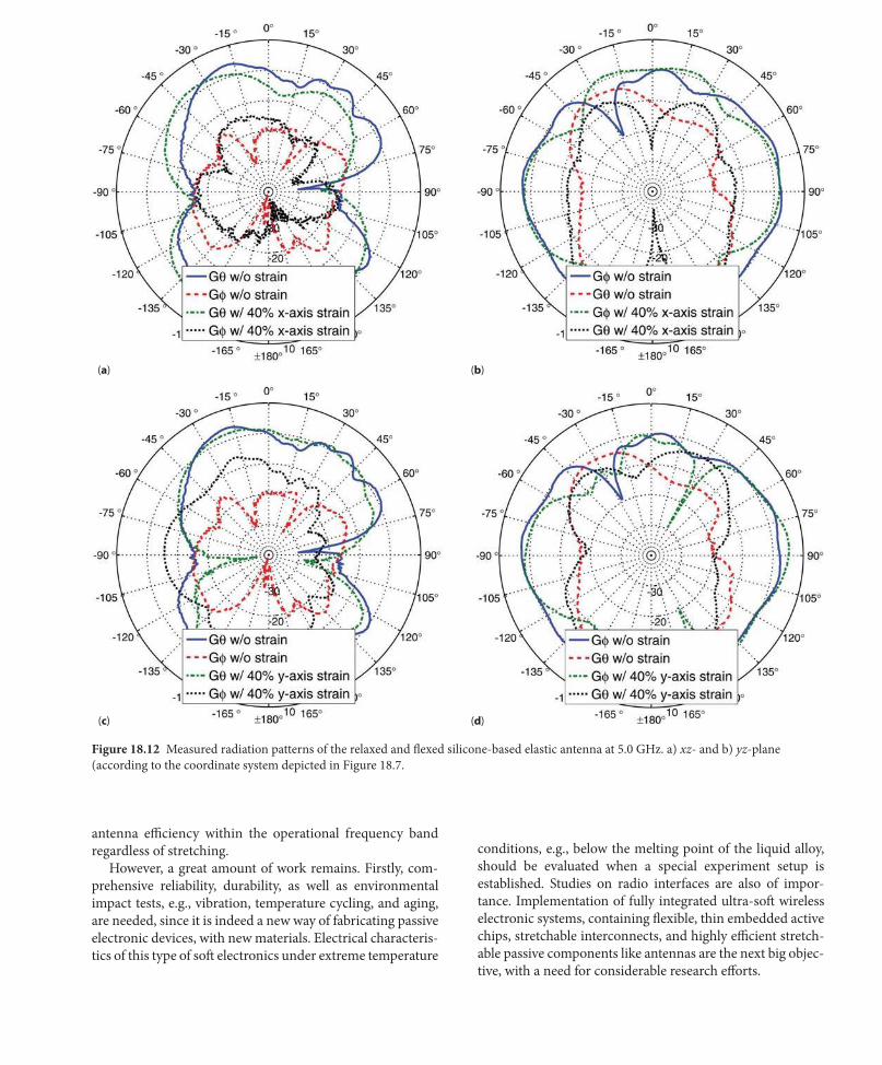
As shown in Figure 18.12, similar simulations and exper-
iments are also performed at 5 GHz, where stronger ripples
and minor asymmetry due to greater disturbance from feed
cable compared to that at lower frequencies, occur in the
radiation patterns. Th e presence of higher order modes at
5 GHz in combination with the increased cable infl uence
degrades the cross-polarization discrimination. Compared
with the experimental data at 2.5 GHz, larger variations on
the measured radiation patterns at 5 GHz are observed, par-
ticularly in its yz-plane in the fl exed state.
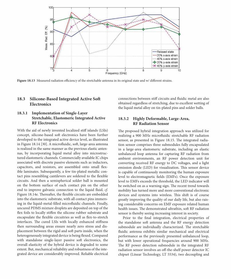
Figure 18.13 presents measured radiation effi ciency over
the entire UWB frequency band. Although the radiation
effi ciency at the lower end of the frequency range decreases
in response to straining, it is still above 70%. Th is, together
with the measured refl ection coeffi cients, indicates that
the silicone-based soft PICA prototype achieves good total
(a) (b)
(c) (d)
Figure 18.11 Measured radiation patterns of the relaxed and fl exed silicone-based elastic antenna at 2.5 GHz. a) xz- and b) yz-plane
(according to the coordinate system depicted in Figure 18.7.
Silicone-Based Soft Electronics 283
antenna effi ciency within the operational frequency band
regardless of stretching.
However, a great amount of work remains. Firstly, com-
prehensive reliability, durability, as well as environmental
impact tests, e.g., vibration, temperature cycling, and aging,
are needed, since it is indeed a new way of fabricating passive
electronic devices, with new materials. Electrical characteris-
tics of this type of soft electronics under extreme temperature
(a) (b)
(c) (d)
Figure 18.12 Measured radiation patterns of the relaxed and fl exed silicone-based elastic antenna at 5.0 GHz. a) xz- and b) yz-plane
(according to the coordinate system depicted in Figure 18.7.
conditions, e.g., below the melting point of the liquid alloy,
should be evaluated when a special experiment setup is
established. Studies on radio interfaces are also of impor-
tance. Implementation of fully integrated ultra-soft wireless
electronic systems, containing fl exible, thin embedded active
chips, stretchable interconnects, and highly effi cient stretch-
able passive components like antennas are the next big objec-
tive, with a need for considerable research eff orts.
284 Concise Encyclopedia of High Performance Silicones
18.3 Silicone-Based Integrated Active Soft Electronics
18.3.1 Implementation of Single-Layer Stretchable, Elastomeric Integrated Active RF Electronics
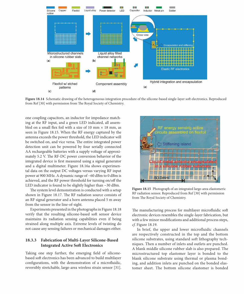
With the aid of newly invented localized stiff islands (LSIs)
concept, silicone-based soft electronics have been further
developed to the integrated active device level, as illustrated
in Figure 18.14 [30]. A microfl uidic, soft , large-area antenna
is realized in the same manner as the previous elastic anten-
nas, by incorporating liquid metal alloy into microstruc-
tured elastomeric channels. Commercially available IC chips
associated with discrete passive elements such as inductors,
capacitors, and resistors, are assembled onto small fl ex-
ible laminates. Subsequently, a few tin-plated metallic con-
tact pins resembling cantilevers are soldered to the fl exible
circuits. And then a semispherical solder ball is mounted
on the bottom surface of each contact pin on the other
end to improve galvanic connection to the liquid fl uid, cf.
Figure 18.14e. Th ereaft er, the fl exible circuits are embedded
into the elastomeric substrate, with all contact pins immers-
ing in the liquid-metal-fi lled microfl uidic channels. Finally,
uncured PDMS mixture droplets are deposited on top of the
fl ex foils to locally stiff en the silicone rubber substrate and
encapsulate the fl exible circuitries as well as fl ex-to-stretch
interfaces. Th e cured LSIs with locally enhanced stiff ness
then surrounding areas ensure nearly zero stress and dis-
placement between the rigid and soft parts inside, when the
heterogeneously integrated device is being fl exed. Compared
with standalone single-layer passive soft electronics, the
overall elasticity of the hybrid device is degraded to some
extent. But, mechanical reliability and robustness of the inte-
grated device are considerably improved. Reliable electrical
connections between stiff circuits and fl uidic metal are also
obtained regardless of stretching, due to excellent wetting of
the liquid metal alloy on tin-plated pins and solder balls.
18.3.2 Highly Deformable, Large-Area, RF Radiation Sensor
Th e proposed hybrid integration approach was utilized for
realizing a 900 MHz microfl uidic stretchable RF radiation
sensor, as presented in Figure 18.15. Th e integrated radia-
tion sensor comprises three submodules fully encapsulated
in a large-area elastomeric substrate, including an elastic
unbalanced loop antenna for capturing RF radiation from
ambient environments, an RF power detection unit for
converting received RF energy to DC voltages, and a light
emission diode (LED) for visualization. Th is sensor device
is capable of continuously monitoring the human exposure
level to electromagnetic fi elds (EMFs). Once the exposure
level to EMFs exceeds the threshold, the LED indicator will
be switched on as a warning sign. Th e recent trend towards
mobility has turned more and more conventional electronic
devices and systems into wireless. Th is shift is of course
greatly improving the quality of our daily life, but also rais-
ing considerable concerns on EMF exposure related human
health issues. Th e demonstrated ultrathin, soft RF radiation
sensor is thereby seeing increasing interest in society.
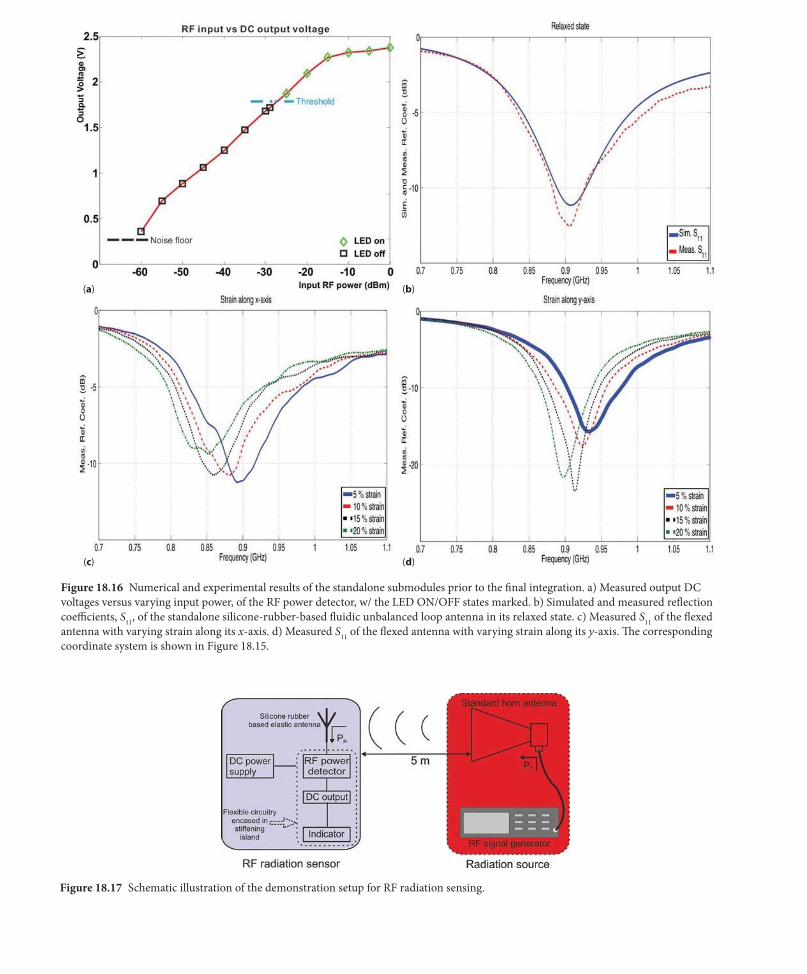
Prior to the fi nal integration, electrical properties of
the standalone soft antenna and the RF energy detection
submodule are individually characterized. Th e stretchable
fl uidic antenna exhibits similar mechanical and electrical
performance as the previously presented unbalanced loop,
but with lower operational frequencies around 900 MHz.
Th e RF power detection submodule in the integrated RF
radiation sensor involves an off -the-shelf power detector IC
chipset (Linear Technology, LT 5534), two decoupling and
Figure 18.13 Measured radiation effi ciency of the stretchable antenna in its original state and w/ diff erent strains.
Silicone-Based Soft Electronics 285
(a) (b)
(c) (d)
(e)
Figure 18.14 Schematic drawing of the heterogeneous integration procedure of the silicone-based single-layer soft electronics. Reproduced
from Ref [30] with permission from Th e Royal Society of Chemistry.
one coupling capacitors, an inductor for impedance match-
ing at the RF input, and a green LED indicated, all assem-
bled on a small fl ex foil with a size of 10 mm × 18 mm, as
seen in Figure 18.15. When the RF energy captured by the
antenna exceeds the power threshold, the LED indicator will
be switched on, and vice versa. Th e entire integrated power
detection unit can be powered by four serially connected
AA rechargeable batteries with a supply voltage of approxi-
mately 5.2 V. Th e RF-DC power conversion behavior of the
integrated device is fi rst measured using a signal generator
and a digital multimeter. Figure 18.16a shows experimen-
tal data on the output DC voltages versus varying RF input
power at 900 MHz. A dynamic range of −60 dBm to 0 dBm is
achieved, and the RF power threshold for turning on/off the
LED indicator is found to be slightly higher than −30 dBm.
Th e system level demonstration is conducted with a setup
shown in Figure 18.17. Th e RF radiation source consists of
an RF signal generator and a horn antenna placed 5 m away
from the sensor in the line-of-sight.
Experiments presented in the photographs in Figure 18.18
verify that the resulting silicone-based soft sensor device
maintains its radiation sensing capabilities even if being
strained along multiple axis. Extreme levels of twisting do
not cause any sensing failures or mechanical damages either.
18.3.3 Fabrication of Multi-Layer Silicone-Based Integrated Active Soft Electronics
Taking one step further, the emerging fi eld of silicone-
based soft electronics has been advanced to build multilayer
confi gurations, with the demonstration of a microfl uidic,
reversibly stretchable, large-area wireless strain sensor [31].
Th e manufacturing process for multilayer microfl uidic soft
electronic devices resembles the single-layer fabrication, but
with a few minor modifi cations and additional process steps,
cf. Figure 18.19.
In brief, the upper and lower microfluidic channels
are respectively constructed in the top and the bottom
silicone substrates, using standard soft lithography tech-
niques. Then a number of inlets and outlets are punched.
A blank middle silicone rubber slab is also prepared. The
microstructured top elastomer layer is bonded to the
blank silicone substrate using thermal or plasma bond-
ing, and addition inlets are punched on the bonded elas-
tomer sheet. The bottom silicone elastomer is bonded
Figure 18.15 Photograph of an integrated large-area elastomeric
RF radiation sensor. Reproduced from Ref [30] with permission
from Th e Royal Society of Chemistry.
286 Concise Encyclopedia of High Performance Silicones
(a) (b)
(c) (d)
Figure 18.16 Numerical and experimental results of the standalone submodules prior to the fi nal integration. a) Measured output DC
voltages versus varying input power, of the RF power detector, w/ the LED ON/OFF states marked. b) Simulated and measured refl ection
coeffi cients, S11
, of the standalone silicone-rubber-based fl uidic unbalanced loop antenna in its relaxed state. c) Measured S11
of the fl exed
antenna with varying strain along its x-axis. d) Measured S11
of the fl exed antenna with varying strain along its y-axis. Th e corresponding
coordinate system is shown in Figure 18.15.
Figure 18.17 Schematic illustration of the demonstration setup for RF radiation sensing.

Silicone-Based Soft Electronics 287
to the previously bonded PDMS layers afterwards. Prior
to filling the upper microfluidic channels with galinstan
fluid metal, the inlet 3 is sealed with a piece of Scotch®
tape. Later, the ventilation outlets in the top silicone
rubber sheet are encapsulated using PDMS prepolymer.
Whereafter, both the inlets 1 and 3 are taped, and galin-
stan alloy is injected into the lower microfluidic channels
from the bottom side. All remaining ventilation outlets
and the inlet 2 are then encapsulated, and the inlets 1 and
3 are reserved for connecting active circuitry in a hetero-
geneously integrated device.
Th e subsequent fabrication process steps are active cir-
cuit assembly and hybrid device integration, which are
similar to the manufacturing and integration processes
presented previously. Schematic illustrations describing the
entire assembly and integration procedure are displayed in
Figure 18.20, and no detailed discussions are presented in
this section.
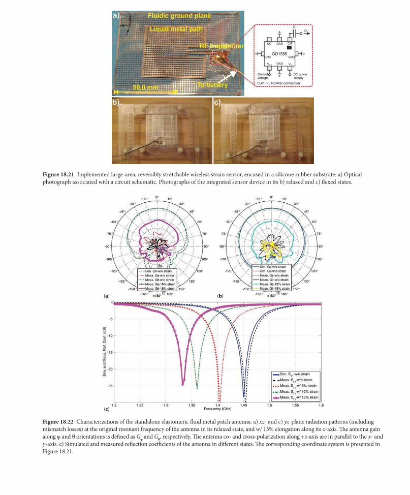
18.3.4 Multilayer, Reversibly Stretchable, Large-Area Wireless Strain Sensor
Th e fi rst silicone based multilayer soft electronic device is
a self-contained wireless strain sensor, fully encapsulated
in a thin large-area silicone rubber substrate, as shown in
Figure 18.21. An elastic fl uid metal microstrip patch antenna
comprising an upper rectangular meshed patch and a lower
ground plane constructed in the same manner, takes up
the major area of the hybrid device. It is worth mention-
ing that this antenna not only serves as a radiator like any
other conventional antenna, but also acts as a sensing device
owing to its varying electrical characteristics in response to
mechanical strains. Th e overall size of the entire integrated
sensor device is slightly larger than the meshed liquid alloy
ground with a size of 100 mm × 80 mm, and roughly four
times as big as the antenna patch. Th ough the liquid metal
patch is the actual strain sensing element, the large ground
(a) (b)
(c) (d)
Figure 18.18 Photographs of the integrated elastomeric RF radiation sensor operating in ordinary offi ce environment: a) in its relaxed state,
b) w/ 15% stretching along its y-axis, c). w/ manually applied 2D strain, and d) w/ manual twisting. Th e presented sensor device was directly
illuminated by an RF radiation source placed 5 m away in the demonstration. Th e coordinate system is seen in Figure 18.15. Reproduced
from Ref [30] with permission from Th e Royal Society of Chemistry.

288 Concise Encyclopedia of High Performance Silicones
(a)
(b)
(c)
(d)
(e)
(f)
(g)
Figure 18.19 Manufacturing process for multilayer silicone-based soft electronics.
(a)
(b)
(c) (d)
(e)
(f)
Figure 18.20 Schematic of the hybrid integration process for a multilayer silicone-based soft electronic device.
Silicone-Based Soft Electronics 289
Figure 18.21 Implemented large-area, reversibly stretchable wireless strain sensor, encased in a silicone rubber substrate: a) Optical
photograph associated with a circuit schematic. Photographs of the integrated sensor device in its b) relaxed and c) fl exed states.
(a) (b)
(c)
Figure 18.22 Characterizations of the standalone elastomeric fl uid metal patch antenna. a) xz- and c) yz-plane radiation patterns (including
mismatch losses) at the original resonant frequency of the antenna in its relaxed state, and w/ 15% elongation along its x-axis. Th e antenna gain
along φ and θ orientations is defi ned as Gφ and G
θ, respectively. Th e antenna co- and cross-polarization along +z-axis are in parallel to the x- and
y-axis. c) Simulated and measured refl ection coeffi cients of the antenna in diff erent states. Th e corresponding coordinate system is presented in
Figure 18.21.
290 Concise Encyclopedia of High Performance Silicones
plane can also serve an eff ective sensing area, and extend the
strain sensing functionality to almost the entire integrated
device. Apart from the self-contained wireless strain sensor,
a custom-designed personal computer (PC)-assisted radio
receiver for remotely collecting, processing, and storing the
measured data wirelessly transmitted from the sensor device
is also realized. It removes the need for costly RF measure-
ment facilities, and signifi cantly reduces the cost for build-
ing up such a system.
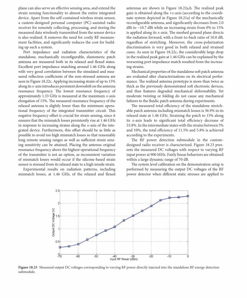
Port impedance and radiation characteristics of the
standalone, mechanically reconfi gurable, elastomeric patch
antenna are measured both in its relaxed and fl exed states.
Excellent port impedance matching around 1.46 GHz along
with very good correlation between the simulated and mea-
sured refl ection coeffi cients of the non-stressed antenna are
seen in Figure 18.22c. Applying increasing strain of up to 15%
along its x-axis introduces persistent downshift on the antenna
resonance frequency. Th e lowest resonance frequency of
approximately 1.33 GHz is measured at the maximum x-axis
elongation of 15%. Th e measured resonance frequency of the
relaxed antenna is slightly lower than the minimum opera-
tional frequency of the integrated transmitter circuit. Th is
negative frequency off set is crucial for strain sensing, since it
ensures that the mismatch losses persistently rise at 1.46 GHz
in response to increasing strains along the x-axis of the inte-
grated device. Furthermore, this off set should be as little as
possible to avoid too high mismatch losses so that reasonably
long remote sensing ranges as well as suffi cient strain sens-
ing sensitivity can be attained. Placing the antenna original
resonance frequency above the highest operational frequency
of the transmitter is not an option, as inconsistent variation
of mismatch losses would occur if the silicone-based strain
sensor is stressed from its relaxed state to a high tensile strain.
Experimental results on radiation patterns, including
mismatch losses, at 1.46 GHz, of the relaxed and fl exed
antennas are shown in Figure 18.22a,b. Th e realized peak
gain is obtained along the +z-axis (according to the coordi-
nate system depicted in Figure 18.21a) of the mechanically
reconfi gurable antenna, and signifi cantly decreases from 2.0
dBi to −10.7 dBi while an increasing strain from 0% to 15%
is applied along its x-axis. Th e meshed ground plane directs
the radiation forward, with a front-to-back ratio of 10.0 dB,
regardless of stretching. Moreover, the cross-polarization
discrimination is very good in both relaxed and strained
cases. As seen in Figure 18.22c, the considerably large drop
in the realized peak gain at 1.46 GHz can be explained by the
worsening port impedance match resulted from the increas-
ing strains.
Mechanical properties of the standalone soft patch antenna
are evaluated aft er characterizations on its electrical perfor-
mance. Th e realized antenna prototype is more than twice as
thick as the previously demonstrated soft electronic devices,
and thus features degraded mechanical deformability. Yet
moderate twisting or folding do not cause any mechanical
failures to the fl uidic patch antenna during experiments.
Th e measured total effi ciency of the standalone stretch-
able patch antenna including mismatch losses is 36.9% in its
relaxed state at 1.46 GHz. Straining the patch to 15% along
its x-axis leads to signifi cant total effi ciency decrease of
33.8%. In the intermediate states with the strains between 5%
and 10%, the total effi ciency of 11.5% and 5.8% is achieved
according to the experiments.
Th e RF power detection submodule in the custom-
designed radio receiver is characterized. Figure 18.23 pres-
ents the measured DC voltages with respect to varying RF
input power at 900 MHz. Fairly linear behaviors are obtained
within a large dynamic range of 70 dB.
Th e system level calibration on the demonstration setup is
performed by measuring the output DC voltages of the RF
power detector when diff erent static stresses are applied to
Figure 18.23 Measured output DC voltages corresponding to varying RF power directly injected into the standalone RF energy detection
submodule.

Silicone-Based Soft Electronics 291
the integrated wireless strain sensor, cf. Figure 18.24. A lin-
ear decline of the measured DC voltages versus increasing
mechanical elongation along the x-axis of the self-contained
sensor device is seen, and can be explained by decreased
resonant frequencies and increased mismatch losses of the
transmitting, elastomeric antenna because of incremental
stretching. As co-polarization components dominate in both
microfl uidic stretchable patch antenna and the receiving horn
in the custom-designed RF receiver, the measured output
voltages with respect to the cross-polarization are considerably
lower than that of the co-polarization, and also exhibit smaller
variations with diff erent strains. Th e steepest voltage decline ver-
sus increasing stretch is found in the case of the co- polarization
measured in an anechoic chamber, cf. Figure 18.25a. When it
comes to ordinary offi ce environment, the presence of refl ec-
tions and scatterings limits the range of voltage variations so as
to degrade the strain sensing sensitivity.
Th e photograph in Figure 18.25b shows the demonstration
of remote sensing of repeated body motion in ordinary offi ce
environment, using the silicone-based soft wireless strain sen-
sor prototype. Periodically repeated dynamic strains of up to
15% along its x-axis, with a period of 10s and a duty cycle
of 50%, are manually applied to the integrated, elastic, strain
sensor. Th e output DC voltages in the PC-assisted RF receiver
varying with mechanical strains applied to the integrated,
body-worn, sensor device are continuously monitored and
recorded. Th e measured data of six cycles, well correlated with
the applied varying tensile strains, are presented in the subplot
in Figure 18.25b, in which six fairly uniform, quasi-rectangular
waves with varying amplitude between 1.28V and 1.55V are
recorded in an overall period of 60s. Th is experimental data
also verifi es that the implemented wireless strain sensor can
Figure 18.24 Measured output DC voltages at the receiver in response to varying mechanical stress applied along the x-axis (according to
the coordinate system in Figure 18.21.
Figure 18.25 Demonstration of remote strain sensing, using the
silicone-based integrated wireless strain sensor: a) Wireless strain
monitoring in an anechoic chamber. b) Remote strain sensing
in ordinary offi ce environment. Th e subplot shows the real-time
recorded data at the PC-assisted RF receiver 5 m away.

292 Concise Encyclopedia of High Performance Silicones
rapidly return to its original state without any hysteresis, once
removing the applied stress. Th is great feature refl ects revers-
ible deformability as well as high degree of elasticity of the
multilayer soft electronic device.
18.4 Conclusion
Recent advances in the emerging fi eld of silicone-based soft
electronics that are able to be compressed, twisted, and stressed
to extreme levels, or be conformed into complex curvilinear
shapes, have been briefl y reviewed. Various techniques and
strategies for realizing fl exible, foldable, stretchable electronic
devices and system have been discussed. As the main focus
of this chapter, elastomeric electronics based on microfl uidic
approaches have been addressed in detail. Fabrication pro-
cesses, hybrid integration techniques, as well as appealing
application examples involving single- and multilayer inte-
grated soft electronic devices have also been presented.
Microfl uidics-based elastic electronics together with
other members in the new class of soft electronics are intro-
ducing a revolution in the world of electronics, and shap-
ing the future for electronics so as to change our daily life
of tomorrow and contribute to our networked society. It is
anticipated that more than 50 billion devices will be wire-
lessly connected by 2020, which would involve units as
intelligent as smart-phones/tablets, and as soft as our newly
invented elastic electronic devices.
Acknowledgements
Th e author currently holds a Young Research Fellow posi-
tion fi nanced by the Swedish Research Council (VR) under
the contract (Avtals-ID: C0486501).
References
1. N. Bowden, S. Brittain, A.G. Evans, J.W. Hutchinson, and
G.M. Whitesides, Nature, Vol. 393, p. 146, 1998.
2. M. Watanabe, H. Shirai, and T. Hirai, Journal of Applied
Physics, Vol. 92, p. 4631, 2002.
3. S.P. Lacour, S. Wagner, Z.Y. Huang, and Z.G. Suo, Applied
Physics Letters, Vol. 82, p. 2404, 2003.
4. S.P. Lacour, J. Jones, S. Wagner, T. Li, and Z.G. Suo, Proceedings
of the IEEE, Vol. 93, p. 1459, 2005.
5. D.H. Kim, J.H. Ahn, W.M. Choi, H.S. Kim, T.H. Kim, J.Z.
Song, Y. Huang, Z.J. Liu, C. Lu, and J.A. Rogers, Science,
Vol. 320, p. 507, 2008.
6. D.H. Kim, J.Z. Song, W.M. Choi, H.S. Kim, R.H. Kim, Z.J.
Liu, Y. Huang, K.C. Hwang, Y.W. Zhang, and J.A. Rogers,
Proceedings of the National Academy of Science of the United
States of America, Vol. 105, p. 18675, 2008.
7. H.C. Ko, M.P. Stoykovich, J. Song, J.V. Malyarchuk, W.M.
Choi, C.J. Yu, J.B. Geddes, J. Xiao, S. Wang, Y. Huang, and J.A.
Rogers, Nature, Vol. 454, p. 748, 2008.
8. J. Lee, J. Wu, M. Shi, J. Yoon, S.I. Park, M. Li, Z. Liu, Y. Huang,
and J.A. Rogers, Advanced Materials, Vol. 8, p. 986, 2011.
9. D.H. Kim, Y.S. Kim, J. Wu, Z. Liu, J. Song, H.S. Kim, Y. Huang,
K.C. Hwang, and J.A. Rogers, Advanced Materials, Vol. 21,
p. 3703, 2009.
10. D.H. Kim, N. Lu, R. Ghaff ari, Y.S. Kim, S.P. Lee, L. Xu, J. Wu,
R.H. Kim, J. Song, Z. Liu, J. Viventi, B. de Graff , B. Elolampi,
M. Mansour, M.J. Slepian, S. Hwang, J.D. Moss, S.M. Won,
Y. Huang, B. Litt, and J.A. Rogers, Nature Materials, Vol. 10,
p. 316, 2011.
11. D.H. Kim, N. Lu, R. Ma, Y.S. Kim, R.H. Kim, S. Wang, J. Wu,
S.M. Won, H. Tao, A. Islam, K.J. Yu, T.I. Kim, R. Chowdhury,
M. Ying, L. Xu, M. Li, H.J. Chung, H. Keum, M. McCormick,
P. Liu, Y.W. Zhang, F.G. Omenetto, Y. Huang, T. Coleman, and
J.A. Rogers, Science, Vol. 333, p.838, 2011.
12. S.I. Park, Y. Xiong, R.H. Kim, P. Elvikis, M. Meitl, D.H. Kim, J.
Wu, J. Yoon, C.J. Yu, Z. Liu, Y. Huang, K.C. Hwang, P. Ferreira,
X. Li, K. Choquette, and J.A. Rogers, Science, 325, p. 977, 2009.
13. A.J. Baca, M.A. Meitl, H.C. Ko, S. Mack, H.S. Kim, J. Dong,
P.M. Ferreira, and J.A. Rogers, Advanced Functional Materials,
Vol. 17, p. 3051, 2007.
14. S. Mack, M.A. Meitl, A.J. Baca, Z.T. Zhu, and J.A. Rogers,
Applied Physics Letters, Vol. 88, p. 213101, 2006.
15. D. Brosteaux, F. Axisa, M. Gonzalez, and J. Vanfl eteren, IEEE
Electronic Device Letters, Vol. 28, p. 552, 2007.
16. B. Huyghe, H. Rogier, J. Vanfl eteren, and F. Axisa, IEEE
Transactions on Advanced Packaging, Vol. 31, p. 802, 2008.
17. R. Carta, P. Jouranda, B. Hermansa, J. Th onéa, D. Brosteauxb,
T. Vervustb, F. Bossuytb, F. Axisab, J. Vanfl eteren, and R.
Puersa, Sensors and Actuators A: Physical, Vol. 156, p. 79, 2009.
18. X. Niu, S. Peng, L. Liu, W. Wen, and P. Sheng, Advanced
Materials, Vol. 19, p. 2682, 2007.
19. T. Sekitani, Y. Noguchi, K. Hata, T. Fukushima, T. Aida, and T.
Someya, Science, Vol. 321, p. 1468, 2008.
20. A.C. Siegel, S.S. Shevkoplyas, D.B. Weibel, D.A. Bruzewicz,
A.W. Martinez, and G.M. Whitesides, Angewandte Chemie
International Edition, Vol. 45, p. 6877, 2006.
21. A.C. Siegel, D.A. Bruzewicz, D.B. Weibel, and G.M. Whitesides,
Advanced Materials, Vol. 19, p. 727, 2007.
22. H. Hu, K. Shaikh, and C. Liu, Proceeding of IEEE Sensor,
Vol. 1, p. 815, 2007.
23. H.J. Kim, C. Son, and B. Ziaie, Applied Physics Letters, Vol. 92,
p. 011904, 2008.
24. H.J. Kim, T. Maleki, P. Wei, and B. Ziaie, Journal of
Microelectromechanical Systems, Vol. 18, p. 138, 2009.
25. S. Cheng, A. Rydberg, K. Hjort, and Z.G. Wu, Applied Physics
Letters, Vol. 94, p. 144103, 2009.
26. S. Cheng, Z.G. Wu, P. Hallbjörner, K. Hjort, and A. Rydberg,
IEEE Transactions on Antennas and Propagation, Vol. 57,
p. 3765, 2009.
27. J.H. So, J. Th elen, A. Qusba, G.J. Hayes, G. Lazzi, and M.D.
Dickey, Advanced Functional Materials, Vol. 19, p. 3632, 2009.
28. M. Kubo, X. Li, C. Kim, M. Hashimoto, B. J. Wiley, D. Ham,
and G.M. Whitesides, Advanced Materials, Vol. 22, p. 2749,
2010.
29. M.R. Khan, G.J. Hayes, J.H. So, G. Lazzi, and M.D. Dickey,
Applied Physical Letters, Vol. 99, p. 013501, 2011.
30. S. Cheng, and Z.G. Wu, Lab on a Chip, Vol. 10, p. 3227, 2010.
31. S. Cheng, and Z.G. Wu, Advanced Functional Materials,
Vol. 21, p. 2282, 2011.
32. Y.N. Xia, and G.M. Whitesides, Annual Review of
MaterialsScience, Vol. 2, p. 153, 1998.


