
CONTROL TECHNIQUES FOR DC-DC BUCK
CONVERTER WITH IMPROVED PERFORMANCE
A THESIS SUBMITTED IN PARTIAL FULFILLMENT
OF THE REQUIRMENTS FOR THE DEGREE OF
Master of Technology (Research)
in
Electrical Engineering
by
Mousumi Biswal
(Roll: 608EE306)
Department of Electrical Engineering
National Institute of Technology Rourkela
March 2011

CONTROL TECHNIQUES FOR DC-DC BUCK
CONVERTER WITH IMPROVED PERFORMANCE
A THESIS SUBMITTED IN PARTIAL FULFILLMENT
OF THE REQUIRMENTS FOR THE DEGREE OF
Master of Technology (Research)
in
Electrical Engineering
by
Mousumi Biswal
Under the supervision of
Prof. Somnath Maity
and
Prof. Anup Kumar Panda
Department of Electrical Engineering
National Institute of Technology Rourkela
March 2011

i
DEPARTMENT OF ELECTRICAL ENGINEERING
NATIONAL INSTITUTE OF TECHNOLOGY, ROURKELA
ROURKELA-769008, ORISSA, INDIA
CERTIFICATE
This is to certify that the thesis entitled, “Control Techniques for Dc/dc Buck Converter with
Improved Performance” submitted to the Department of Electrical Engineering, National
Institute of Technology, Rourkela by Ms. Mousumi Biswal for the partial fulfillment of award of
the degree Master of Technology (Research) is a bona fide record of research work carried out
by her under our supervision and guidance.
The matter embodied in the thesis is original and has not been submitted elsewhere for the award
of any degree or diploma.
In our opinion, the thesis is of standard required for the award of a Master of Technology
(Research) Degree in Electrical Engineering.
Prof. Somnath Maity Prof A. K. Panda
(Supervisor) (Co-Supervisor)

ii
ACKNOWLEDGEMENTS
I would like to express my heartiest gratitude towards my supervisor Prof. (Dr.) Somnath
Maity, and my co-supervisor Prof. (Dr.) A.K Panda, Professor of Electrical Engineering for their
valuable and enthusiastic guidance, help and continuous encouragement during the course of the
present research work. I am indebted to them for having helped to shape the problem and
providing insights towards the solution.
I am very much obliged to Prof. (Dr.) B.D. Subudhi, Professor and Head of the Department
of Electrical Engineering for his valuable suggestions and support.
I am thankful to Prof. (Dr.) K.B Mohanty, Professor of Electrical Engineering and Prof. (Dr.)
Poonam Singh, Professor of Electronics Engineering for their support during the research period.
I would like to give a special thanks to all my friends for all the thoughtful and mind
stimulating discussions, sharing of knowledge which prompted us to think beyond. The help and
co-operation received from the staff of Department of Electrical Engineering is thankfully
acknowledged.
I would like to thank my parents for their prayer, understanding and moral support during
the tenure of research work.
Mousumi Biswal

iii
ABSTRACT
The switched-mode dc-dc converters are some of the most widely used power electronics
circuits for its high conversion efficiency and flexible output voltage. These converters used for
electronic devices are designed to regulate the output voltage against the changes of the input
voltage and load current. This leads to the requirement of more advanced control methods to
meet the real demand. Many control methods are developed for the control of dc-dc converters.
To obtain a control method that has the best performances under any conditions is always in
demand.
Conventionally, the dc-dc converters have been controlled by linear voltage mode and current
mode control methods. These controllers offer advantages such as fixed switching frequencies
and zero steady-state error and gives a better small-signal performance at the designed operating
point. But under large parameter and load variation, their performance degrades. Sliding mode
(SM) control techniques are well suited to dc-dc converters as they are inherently variable
structure systems. These controllers are robust concerning converter parameter variations, load
and line disturbances. SM controlled converters generally suffer from switching frequency
variation when the input voltage and output load are varied. This complicates the design of the
input and output filters. The main objective of this research work is to study different control
methods implemented in dc-dc converter namely (linear controllers, hysteresis control, current
programmed control, and sliding mode (SM) control). A comparison of the effects of the PWM
controllers and the SM control on the dc-dc buck converter response in steady state, under line
variations, load variations is performed.

iv
The thesis shows that, in comparison with the PWM controllers, the SM control provides
better steady-state response, better dynamic response, and robustness against system uncertainty
disturbances. Also the hysteretic controlled converters response to disturbances and load change
right after the transient take place and they give excellent transient performance. It does not
require the closed loop compensation network and results with a lesser component count and
small size in implementation. Hence, hysteretic control is considered as the simplest and fastest
control method. The dc-dc buck converter employing current hysteresis control scheme is given
in thesis. The result shows that hysteresis control converters have inherently fast response and
they are robust with simple design and implementation.
A hysteretic current control technique for a tri-state buck converter operating in constant
switching frequency is designed and its behavior is studied by making the use of essential tools
of sliding mode control theory because dc-dc buck converter is a variable structure system due to
the presence of switching actions. The principle of operation of tristate dc-dc buck converter is
explained. The converter response is investigated in the steady-state region and in the dynamic
region. The problem of variable switching frequency is eliminated without using any
compensating ramp.
Keywords: Hysteresis control, Sliding mode control, Dc-dc buck converter, variable structure
system.
v
CONTENTS
Title Page No.
Certificate
Acknowledgement
Abstract
Contents
List of Figures
Nomenclature
Abbreviations
i
ii
iii
v
viii
x
xii
CHAPTER 1: INTRODUCTION
1.1
1.2
1.3
1.4
1.5
1.6
Motivation
Literature Review
Basic Principles of Sliding-mode Control
Review on Sliding-mode Control Theory
Objective and Scope of this Dissertation
Organization of Thesis
1
4
10
11
15
16
CHAPTER 2: CONTROL METHODS FOR DC-DC CONVERTER
2.1
2.2
2.3
Introduction
The Dc-dc Buck Converter
Modes of Operation of Dc-dc Buck Converter
2.3.1 Continuous Conduction Mode (CCM)
2.3.2 Discontinuous Conduction Mode (DCM)
17
18
20
20
21

vi
2.4
2.5
2.6
2.7
Control Methods for Dc-dc Converter
2.4.1 Voltage-Mode Controlled Buck Converter
2.4.2 Current-Mode Controlled Buck Converter
Sliding-mode control for Dc-dc Buck Converter
2.5.1 System Modeling
2.5.2 Design of SM Controller
2.5.3 Derivation of SM Existence Condition
Simulation Results
Conclusion
22
22
25
29
29
31
33
38
45
CHAPTER 3: FIXED FREQUENCY HYSTERESIS CONTROLLER
3.1
3.2
3.3
3.4
3.5
3.6
3.7
Introduction
Variable switching Frequency Hysteretic Controllers
3.2.1 Hysteretic Voltage-Mode Controllers
3.2.2 Hysteretic Current-Mode controllers
Simulation Results
Constant Switching Frequency Current-mode Hysteretic Controller
3.4.1 Basic Concept of Operation
3.4.2 Mathematical Analysis of proposed Controller
Model including parasitic elements
Simulation Results
Conclusion
46
47
47
48
50
54
54
57
64
65
74

vii
CHAPTER 4: CONCLUSIONS AND FUTURE SCOPES
4.1
4.2
Conclusions
Scope for Future work
71
73
REFERENCES
74

viii
LIST OF FIGURES
Figure Title Page
Figure 1.1(a) Phase Plot for ideal SM Control 10
Figure 1.1(b) Phase Plot for actual SM control 10
Figure 2.1 Buck dc-dc converter topology 18
Figure 2.2(a) Buck Converter when switch turns on 19
Figure 2.2(b) Buck Converter when switch turns off 19
Figure 2.3(a) Inductor current waveform of PWM converter in CCM 21
Figure 2.3(b)
Inductor current waveform of PWM converter in the boundary of
CCM and DCM
21
Figure 2.3(c) Inductor current waveform of PWM converter in DCM 21
Figure 2.4 Block diagram of voltage mode controller 22
Figure 2.5 Current-mode controlled dc-dc buck converter 25
Figure 2.6 Peak Current Mode Control 28
Figure 2.7 Inductor Current waveform with compensating ramp 28
Figure 2.8 Basic structure of an SMC buck converter system 29
Figure 2.9 Sliding line on 1 2x x phase plane 33
Figure 2.10 Region of Existence of SM mapped in the phase plane 35
Figure 2.11 Evolution of phase trajectory in phase plane for 1 2RCc c 35

ix
Figure 2.12 Phase plane diagram for 1 2RCc c 36
Figure 2.13 Phase plane diagram for 1 2RCc c 36
Figure 2.14 Chattering phenomena of SM control 37
Figure 2.15
Output Voltage response due to a step change in load resistance
from 15Ω to 10Ω and back to 15Ω
39
Figure 2.16
Inductor Current response due to a step change in load resistance
from 15Ω to 10Ω and back to 15Ω
39
Figure 2.17
Output Voltage response for a change input voltage from 20V to
15V and back to 20V
40
Figure 2.18
Inductor Current response for a change input voltage from 20V to
15V and back to 20V
40
Figure 2.19
Output Voltage response due to a step change in load resistance
from 15Ω to 10Ω and back to 15Ω
42
Figure 2.20
Inductor Current response due to a step change in load resistance
from 15Ω to 10Ω and back to 15Ω
42
Figure 2.21
Output Voltage response for a change input voltage from 20V to
15V and back to 20V
43
Figure 2.22
Inductor Current response for a change input voltage from 20V
to 15V and back to 20V
43
Figure 2.23
Phase plane plot under step load transient from
for SM control
44
Figure 3.1 Voltage hysteresis control 47
Figure 3.2 Hysteretic CM controlled buck converter 48

x
Figure 3.3
Transient response of the hysteretic current controlled buck
converter when load from 15Ω to 10Ω and back to 15Ω
51
Figure 3.4
Transient response of the hysteretic current controlled buck
converter when input voltage from 20V to 15V and back to 20V
52
Figure 3.5 Phase plane diagram with load transient 53
Figure 3.6 A tristate buck converter configuration 55
Figure 3.7(a)
Equivalent circuits under different modes of operation: mode 1
( 1 sD T )
55
Figure 3.7(b)
Equivalent circuits under different modes of operation: mode 2
( 2 sD T )
55
Figure 3.7(c)
Equivalent circuits under different modes of operation: mode 3
( 3 sD T )
56
Figure 3.8
Inductor current waveform of a tristate buck converter
showing the switch conditions
57
Figure 3.9
Schematic diagram of the hysteretic controller for tristate buck
converter
57
Figure 3.10 Schematic diagram of pulse generator circuit 58
Figure 3.11 Model of tristate buck converter with all parasitic elements 64
Figure 3.12
Startup transient performance of converter with the proposed
controller
66
Figure 3.13 The proposed current hysteretic controller operating principle 67
Figure 3.14
Transient response for a change in load from 15Ω to 10Ω and
back to 15Ω
68

xi
Figure 3.15 Output voltage response from load transient 10Ω to 15Ω 68
Figure 3.16 Load transient response from 15Ω to 10Ω 69
Figure 3.17
Load transient response from 15Ω to 10Ω for conventional
current hysteretic control method
69
Figure 3.18
Transient response due to a step change in reference voltage from
6V to5V and back to 6 V
70
Figure 3.19 Phase plane diagram 71
Figure 3.20 Magnified view showing the phase trajectory and hysteresis band 71
Figure 3.21 The output voltage ripple and inductor current ripple in steady
state operation by considering the effect of parasitic elements
72
Figure 3.22 The inductor current ripple in steady state operation
73

xii
NOTATIONS
Symbol
x State vector
f Function vector with n-dimension
u Discontinuous control input
S Sliding surface (manifold)
,f f State velocity vector
,N Nf f Normal vectors
S Gradient of sliding surface
,e e Representative points
Constant value
equ Equivalent continuous control input
wS controlled switch
L Inductance
C capacitance
R Load resistance
Li Inductor current
Ci Capacitor current
Cv Capacitor voltage

xiii
inv Input voltage
0v Output voltage
conv Control voltage
refV Reference voltage
,p Ik k Proportional gain and integral gain of P-I controller
1k Voltage reduction factor
rampv Sawtooth or Ramp voltage
,U LV V Upper and Lower threshold voltages
q Switching signal
h Switching hypersurface
refi Reference current
fR Proportionality factor
1x Voltage error
2x Voltage error dynamics
1 2, Line equations in phase plane
Small constant value
D Diode
sf Switching frequency
ST Time period of external clock pulse

xiv
ABBREVIATIONS
SMPS Switched Mode Power Supply
CCM Continuous Conduction Mode
DCM Discontinuous Conduction Mode
SM Sliding Mode
VSC Variable Structure Control
VSS Variable Structure System
P Proportional Control
PD Proportional derivative Control
PID Proportional integral derivative Control
EMI Electromagnetic Interference
HM Hysteresis Modulation
PWM Pulse Width Modulation
GPI Generalized proportional integral
PCCM
Pseudo continuous conduction mode
RP Representative Point
VMC Voltage mode control
CMC Current mode control
PCMC Peak current mode control


1
CHAPTER 1
Introduction
1.1 Motivation
The switched mode dc-dc converters are some of the simplest power electronic
circuits which convert one level of electrical voltage into another level by switching
action. These converters have received an increasing deal of interest in many areas. This
is due to their wide applications like power supplies for personal computers, office
equipments, appliance control, telecommunication equipments, DC motor drives,
automotive, aircraft, etc. The analysis, control and stabilization of switching converters
are the main factors that need to be considered. Many control methods are used for
control of switch mode dc-dc converters and the simple and low cost controller structure
is always in demand for most industrial and high performance applications. Every control
method has some advantages and drawbacks due to which that particular control method
consider as a suitable control method under specific conditions, compared to other control
methods. The control method that gives the best performances under any conditions is
always in demand.
The commonly used control methods for dc-dc converters are pulse width modulated
(PWM) voltage mode control, PWM current mode control with proportional (P),
proportional integral (PI), and proportional integral derivative (PID) controller. These
conventional control methods like P, PI, and PID are unable to perform satisfactorily
under large parameter or load variation. Therefore, nonlinear controllers come into

2
picture for controlling dc-dc converters. The advantages of these nonlinear controllers are
their ability to react suddenly to a transient condition. The different types of nonlinear
controllers are hysteresis controller, sliding mode controller, boundary controller, etc.
The hysteresis control methods for power converters are also gaining a lot of interest
due its fast response and robust with simple design and implementation. The hysteresis
controllers react immediately after the load transient takes place. Hence the advantages of
hysteretic control over other control technique include simplicity, do not require feedback
loop compensation, fast response to load transient. However, the main factors need to be
considered in case of hysteresis control are variable switching frequency operation and
stability analysis.
The dc-dc converters, which are non-linear and time variant system, and do not lend
themselves to the application of linear control theory, can be controlled by means of
sliding-mode (SM) control, Which is derived from the variable structure control system
theory (VSCS). Variable structure systems are systems the physical structures of which
are changed during time with respect to the structure control law. The instances at which
the changing of the structure occurs are determined by the current state of the system.
Due to the presence of switching action, switched-mode power supplies (SMPS) are
generally variable structured systems. Therefore, SM controllers are used for controlling
dc-dc converters.
SM control method has several advantages over the other control methods that are
stability for large line and load variations, robustness, good dynamic response, simple
implementation. Ideally, SM controllers operate at infinite switching frequency and the
controlled variables generally track a particular reference path to achieve the desired
steady state operation. But an infinite switching frequency is not acceptable in practice,
especially in power electronic circuits and therefore a control technique that can ensure a

3
finite switching frequency must implemented. The extreme high speed switching
operation results in switching losses, inductor and transformer core loss and
electromagnetic-interference (EMI) generation. Variable switching frequency also
complicates the design of input and output filter. Hence, for SM controllers to be
applicable to dc-dc converters, their switching frequency should be constricted within a
practical range.
Though SM control compiles of various advantages, SM controlled converters suffers
from switching frequency variation when the input voltage and output load are varied.
Hence there are many control methods which have been developed for fixed switching
frequency SM control such as fixed frequency PWM based sliding mode controllers,
adaptive SM controller, digital fuzzy logic SM controller, etc. In case of adaptive control,
adaptive hysteresis band is varied with parameter changes to control and fixate the
switching frequency. But, these methods require more components and are unattractive
for low cost voltage conversion applications.
The different types of hysteresis controller are hysteretic voltage-mode controller, V2
controller, and hysteretic current-mode controllers. The current hysteresis control
incorporates both the advantages of hysteresis control and current mode control. It can be
implemented using two loop control method. The error between the actual output voltage
and reference voltage gives the error voltage. A PI control block can use the voltage error
signal to provide a reference current for hysteresis control. This is also called sliding
mode control for dc-dc converter. Therefore, the current mode hysteretic controller can be
considered as a sliding mode control system and the analysis of hysteretic controller can
be done as per sliding mode control theory. The essential tools of this nonlinear control
theory can be introduced for the study of the behavior of hysteresis controller.

4
Therefore, the motivation of this thesis is to improve the performance of a dc-dc buck
converter through controller improvements. Hence, this thesis focused on the design and
analysis of a fixed frequency hysteretic current mode controller with improved
performance for dc-dc buck converter circuit. The problem of switching frequency
variation is alleviated with simplicity in controller design.
1.2 Literature Review
The dc-dc switching converters are the widely used circuits in electronics systems.
They are usually used to obtain a stabilized output voltage from a given input DC voltage
which is lower (buck) from that input voltage, or higher (boost) or generic (buck–boost)
[1]. Most used technique to control switching power supplies is Pulse-width Modulation
(PWM) [2]. The conventional PWM controlled power electronics circuits are modeled
based on averaging technique and the system being controlled operates optimally only for
a specific condition [3]-[4]. The linear controllers like P, PI, and PID do not offer a good
large-signal transient (i.e. large-signal operating conditions) [4]-[5].
Therefore, research has been performed for investigating non-linear controllers. The
main advantages of these controllers are their ability to react immediately to a transient
condition. The different types of non-linear analog controllers are: (a) hysteretic current-
mode controllers, (b) hysteretic voltage-mode/V2 controllers, (c) sliding-mode/boundary
controllers. Advantages of hysteretic control approach include simplicity in design and do
not require feedback loop compensation circuit. M. Castilla [6]-[8] proposed voltage-
mode hysteretic controllers for synchronous buck converter used for many applications.
The analysis and design of a hysteretic PWM controller with improved transient response
have been proposed for buck converter in 2004[9].

5
The use of SM control techniques in variable structure systems (VSS) makes these
systems robust to parameter variations and external disturbances [10]-[11]. Sliding mode
control has a high degree of design flexibility and it is comparatively easy to implement.
This explains its wide utilization in various industrial applications, e.g. automotive
control, furnace control, etc. [10]-[12]. Switched mode dc-dc converters represent a
particular class of the VSS, since there structure is periodically changed by the action of
controlled switches and diodes. So it is appropriate to use sliding mode controllers in dc-
dc converters [13]. It is known that the use of SM (nonlinear) controllers can maintain a
good regulation for a wide operating range. So, a lot of interest is developed in the use of
SM controllers for dc-dc converters [14]-[63]. Siew-Chong Tan presented a detail
discussion on the use of SM control for dc-dc power converters [15].
In 1983 and 1985, the implementation of sliding mode control for dc-dc converters is
first presented [13]-[14]. Then SM controller is applied in higher order converters in 1989
[16]. Huang et al. applied SM control for cuk switching regulator. After this, a series of
related works on the cuk converter was carried out [17]-[20]. Fossas and Pas [21] applied
a second-order SM control algorithms to buck converter for reduction of chattering.
Then, two types of SM-control for boost and buck-boost converters: one using the method
of stable system centre [22] and the other using sliding dynamic manifold [23] is
proposed by Yuri B. Shtessel. Sira-Ramirez [24] proposed a hysteresis modulation type
of SM controller to achieve a generalized proportional integral (GPI) continuous control
of a buck converter. Sira-Ramirez also presented a tutorial revisit of traditional sliding
mode control approach for the regulation of dc-dc power converters, of the „buck‟,
„boost‟ and „buck-boost‟ type and proposed the use of GPI control technique to improve
system robustness [25].

6
Raviraj and Sen presented a comparative study on buck converter‟s performance when
controlled by PI, SM, and fuzzy-logic controllers in 1997 [26]. They showed that there
are certain similarities in the system behavior between fuzzy-logic and SM controllers.
SM controller is also applied on parallel connected dc-dc converters. Donoso-Garcia et al.
[27] and shtessel et al. [28] proposed the use of SM control for current distribution and
output-voltage regulation of multiple modular dc-dc converters. Sira-Ramirez and Rios-
Bolivar [29] applied extended linearization method in SM-controller design that has
excellent self scheduling properties. They also proposed to combine a SM control scheme
with passivity-based controllers into the dc-dc converter that enhances its robustness
properties [30]-[31]. In 1997, Carrasco et al. [32] proposed neural controller with SM
controllers to improve the robustness, stability and dynamic characteristic of the PWM
dc/dc power circuit with power factor corrector.
The nonlinear behavior exhibited by current mode controlled boost converter is
studied by Morel [33]-[35]. Then, he introduced a practical SM control method aiming to
eliminate chaotic behavior and keep the desired current-controlled property. The standard
method (slope compensation) only partly cures this major drawback and, even though it
eliminates chaos, the converter is not current-controlled any more. He concluded that the
proposed method does not only provide stability, it also increases the input voltage
variation domain for which the system remained stable.
Mattavelli et al. [36] proposed a general-purpose sliding-mode controller, which is
applicable to most dc-dc converter topologies. The circuit complexity is same as current-
mode controllers and it provides extreme robustness and speed of response against line,
load and parameter variations. The same group derived small signal models for dc-dc
converters with SM control, which allows the selection of control coefficients, the
analysis of parameter variation effects, the evaluation of the closed loop performances

7
like audio susceptibility, output and input impedances, and reference to output transfer
function [37].
Despite various advantages of SM controller, the practical implementation of this
controller for dc-dc converters is rarely discussed. This is due to the lack of understanding
in its design and systematic procedure for developing such controllers. Escobar et al. [38]
performed experiments to compare five different control algorithms on dc-dc boost
converter. He concluded that nonlinear controllers provide a promising alternative to the
linear average controller. Alarcon et al. [39] presented the design of analog IC SM
control prototype with linear sliding surface for switching converters. Ahmed et al. [40],
[41] presented an analysis and experimental study of SM controlled buck converter. They
also showed the implementation of the SM controller for buck-boost converter through
control desk dSPACE [42]. Dominguez et al. [43] presented a stability analysis of buck
converter with input filter by means of SM control technique. Zhang li and QIU Shui-
sheng implemented Proportional-Integral sliding mode controller in dc-dc converters.
They showed that the implementation of PI SM control is simpler than other SM control
schemes and steady state error is eliminated [44]. Castilla et al. [45] created a novel
design methodology of SM control schemes for quantum resonant converters. The
method is based on the imposition of a specified output-voltage dynamic response, and it
provides a set of sliding surfaces guaranteeing high robustness and large signal stability.
Siew-Chong Tan presented a systematic approach for designing a practical SM controller
for buck converter [46].
An ideal SMCT (sliding mode control technique) operates at infinite switching
frequency [46]-[47]. This infinite switching frequency invites inductor, transformer core
losses and electromagnetic interference noise issues. Hence, practical SM controllers are
operated at finite switching frequencies only. Thus, ideal SM is brought to quasi-sliding

8
mode .The frequency limited SM controllers are generally called as Quassi –sliding mode
controllers [47]. Cardoso et al. [48] proposed several methods to constrict the switching
frequency of the SM controlled converters. Switching frequency variation can be
eliminated by employing PWM based SM control instead of hysteresis modulation (HM)
[49].
Nguyen and Lee proposed an adaptive hysteresis type of SM controller for buck
converter [50]. They again proposed an indirect implementation of SM controllers in
buck converter to achieve constant switching frequency operation [51]. Chiacchiarini et
al. [52] performed experiment to compare the performance of buck converter controlled
by analog and also for digital sliding-mode controllers. Sira-Ramirez et al. [53] proposed
a geometric approach to map the PWM feedback control onto SM control and provide the
equivalence between SM and PWM controller [54]. The discrete control input is replaced
by a smooth analytic function of the state, known as the duty ratio.
Mahadevi et al. [55] proposed state space averaging method to PWM based SM
controlled dc-dc converters with a constant switching frequency. They also applied neural
networks into their PWM-based SM controlled converters [56]. Siew-Chong Tan
proposed a new adaptive sliding mode controller for buck converter in continuous
conduction mode of operation [57]. They concluded that adaptive SM controlled
converter has faster dynamic response with reduced steady state error when it operated
above the nominal load, and it eliminates overshoots and ringing in the transient response
when operated below the nominal load. In 2004, a digital fuzzy logic SM-like controller
that has zero steady state error and fixed switching frequency is proposed by Perry et al.
[58]. Ianneli and Vasca proposed method of dithering to SM controlled converters for
maintaining a finite and constant switching frequency [59].

9
Steady-state switching frequency of sliding mode controlled dc-dc converters is
generally affected by line and load variation. For line variation, an adaptive feed forward
control that varies the hysteresis band in the hysteresis modulator of the SM controller in
the event of any change of the line input voltage and for load variation, an adaptive
feedback controller that varies the control parameter with the change of output load is
proposed by Siew-Chong Tan [60]. Dc-dc converters can be operated either in continuous
conduction mode (CCM) or in discontinuous conduction mode (DCM). Dc-dc converters
that operated in DCM provide faster transient response (due to its low inductance) at the
expense of higher device stresses. He also presented a fixed frequency PWM based
sliding mode controllers for dc-dc converters operating in DCM [62]-[63].
Buck converter when operated in CCM, gives a continuous output current, with
smaller current ripple and low switching noise. CCM operation is usually preferred for
large current applications, because it can deliver more current than the converter
operating in DCM. However, a DCM converter has a much faster transient response and a
loop gain that is easier to compensate than a CCM converter. Hence, for fulfill of both the
requirements, a new converter that combines the advantage of both CCM and DCM
converters is developed. Converters operate in a new operation mode-the pseudo CCM.
This new switching converter that is operating in pseudo-continuous-conduction-mode
(PCCM) with freewheel switching control is proposed by Dongsheng Ma and Wing-Hung
Ki [64]-[65]. They showed that pseudo CCM buck converter has much improved current
handling capability with reduced current and voltage ripple.

10
1.3 Basic principles of SM control
The basic idea of SM control is to design first a sliding surface in state space and then
the second is to design a control law direct the system state trajectory starting from any
arbitrary initial state to reach the sliding surface in finite time, and finally it should come
to a point where the system equilibrium state exists that is in the origin point of the phase
plane. The existence, stability and hitting condition are the three factors for the stability of
sliding mode control. SM control principle is graphically represented in Figure 1, where
0S , represent the sliding surface and x1 and x2 are the voltage error variable and
voltage error dynamics respectively. The sliding line (when it is a two variable SM
control system in two-dimensional plane) divides the phase plane into two regions. Each
region is specified with a switching state and when the trajectory arrives at the system
equilibrium point, the system is considered as stable.
(a)
(a) (b)
Figure 1.1: Phase Plot for (a) ideal SM Control (b) actual SM control
If the hysteresis band around the sliding line becomes zero, then system is said to be
operated with ideal SM control. But, from the practical point of view, this is not possible

11
to achieve. Hence, the actual SM control operation that is when the hysteresis band is not
ideal having a finite switching frequency is shown in figure 1.1(b) [46].
1.4 Review on SM control theory
The SM control theory is a well discussed topic [12], [61]. In this section a general
review on SM control theory is presented. Let us consider a general system with scalar
control as an example for better understanding of design procedure of SM control.
( , , )
dxf x t u
dt (1.1)
where x is the column vector that represents the state of the system, f is a function
vector with n dimension, u is the control input that makes the system discontinuous. The
function vector f is discontinuous on the sliding surface ( , ) 0S x t , which can be
represented as,
for
for
( , , ) ( , )>0( , , )
( , , ) ( , )<0
f x t u S x tf x t u
f x t u S x t (1.2)
where ( , ) 0S x t is the sliding surface (sliding manifold). The system is in sliding mode
if its representative point (RP) moves on the sliding surface ( , ) 0S x t .
Existence condition and reaching condition are two requirements for a stable SM
control system. The existence condition of sliding mode requires that the phase
trajectories belongs to the two regions, created by the sliding line, corresponding to the
two different values of the vector function f must be directed towards the sliding line.
While approaching the sliding line from the point which satisfies ( , ) 0S x t , the
corresponding state velocity vector f must be directed toward the sliding surface, and

12
the same happens for the points above ( , ) 0S x t for which the corresponding state
velocity vector is f .
The normal vectors ( ,N Nf f ) of the function f are orthogonal to the sliding surface or
the sliding line, which is given by,
0 0
0 0
lim lim
lim lim
0 . 0
0 . 0
NS S
NS S
f S f
f S f (1.3)
where S is the gradient of surface S . This is expressed as
1
.N
i
i i
dS S dxS f
dt x dt (1.4)
Therefore, in mathematical terms the sliding-mode existence condition is represented as
0
lim 0S
dSS
dt (1.5)
When the inequality given in equation (2.5) holds in the entire state space, then this is the
sufficient condition for the system RP to reach the sliding surface.
The reaching condition means the system RP will reach the sliding surface within
finite time interval. The scalar discontinuous input u at any instant depends upon the
system RP in state space at that instant. Hence, the control input for the system in (1.1)
can be written in mathematical form as,
for
for
( , ) 0
( , ) 0
u S x tu
u S x t (1.6)
where u and u are the switching states which belong to the region ( ) 0S x and
( ) 0S x respectively. Let e and e be the steady state RPs corresponding to the

13
inputs u+ and u
-.Then a sufficient condition for reaching the sliding surface is given by:
( , ) 0
( , ) 0
e S x t
e S x t (1.7)
If the steady state point for one substructure belongs to the region of phase space reserve
to the other substructure, then sooner or later the system RP will hit the sliding surface.
Then, the behavior of dc-dc switching converter when operated in sliding mode with the
equivalent input is described below.
For the dc-dc converter system the state space model can be written as,
( , ) ( , )dx
f x t g x t udt
(1.8)
The control input u is discontinuous on sliding surface ( , ) 0S x t , while f and g are
continuous function vectors. The sliding surface is a combination of state variables as
( , )S x t kx (1.9)
Under SM control, the system trajectories stay on the sliding surface, therefore:
( , ) 0
( , ) 0
S x t
dS x t
dt
(1.10)
1
ni
i i
dxdS S
dt x dt
dxS
dt
dxk
dt
(1.11)

14
where k is a 1 by n matrix, the elements of which are the derivatives of the sliding
surface with respect to the state variables (gradient vector) and is some constant value.
Using equations (1.8) and (1.11) leads to
( , ) ( , ) 0eq
dxk kf x t kg x t u
dt (1.12)
where the discrete control input u was replaced by an equivalent continuous control
input equ , which maintains the system evolution on the sliding surface. The expression for
the equivalent control is given as
1( ) ( , )equ kg kf x t (1.13)
Substituting equation (1.13) into equation (1.8) gives
1[ ( ) ] ( , )
dxI g kg k f x t
dt (1.14)
Equation (1.14) describes the system motion under the SM control. The system should be
stable around any operating point. For satisfying the stability condition of the SM control,
the created sliding surface will always direct the state trajectory towards a point where
system stable equilibrium exits. This is generally accomplished through the design of the
sliding coefficients to meet the desired dynamical property. This is possible by using the
invariance property. Since in sliding mode operation, the state trajectory will track the
path of the sliding surface to a point of stability, the dynamical property of the system can
be determined by proper selection of sliding coefficient.
.

15
1.5 Objective and Scope of this Dissertation
Control of switching converters is an interesting research area. The dynamic
performance improvement and stability of switching power converters has always been a
main concern. Most times the analysis is based on linear, small signal formalism, in order
to tune and then design new schemes. Hence, the scope of the work is motivated by a
need of new tools and techniques in order to explore better solutions.
Since dc-dc converters are nonlinear time variant systems, they represent a hard task for
control design. As dc-dc converters are variable structured in nature, so nonlinear
controllers are proved to be effective for the control of dc-dc converters. These controllers
respond immediately to the transient conditions. The types of non-linear controllers
include hysteretic controllers, sliding-mode/boundary controllers, etc. Advantages of
hysteretic control technique include simplicity in design and do not require feedback loop
compensation circuitry. SM controllers are well known for robustness and stability. SM
control with infinite operation frequency challenges the feasibility of applying SM
controllers to switching power converters. Extreme high switching frequency results in
serious EMI, switching losses. Therefore the constant frequency operation becomes the
key point to be considered for practical controller design of switching converter.
The buck converter is the most widely used dc-dc converter topology in power
management and microprocessor voltage regulator applications. Here the analysis and
design of controller is made on the simplest dc-dc converter circuit i.e. the buck converter
circuit. The main objective of this research work is to study different control methods and
to design an efficient controller with improved performance. The proposed technique
requires less component and simple for implementation and eliminates the problem of
variable switching frequency.

16
1.6 Organization of Thesis
The contents of each chapter are organized as follows:
Chapter 1: The importance of switch mode dc-dc converter for various applications is
given. This chapter explains the various types of linear and nonlinear control techniques.
The problems associated with the control methods for dc-to-dc converters are discussed.
A literature survey in detail is done on the control techniques available. The basic
principle of SM control theory is described.
Chapter 2: In this chapter the most commonly used analog PWM control method for dc-
dc buck converter are studied. Also the sliding mode control technique for buck converter
is analyzed, and comparative studies of the discussed control methods are given. The
advantage of using sliding-mode controller is discussed. The result shows that SM
controller offers better steady state and transient response than other control methods.
Chapter 3: This chapter describes a simple and brief study on hysteretic controllers. The
hysteretic control converters are inherently fast response and simple in design. Therefore,
the use of hysteretic controller for buck converter is given. This chapter also discusses
about the operation of tri-state buck converter. The design of a fixed frequency hysteretic
controller for tri-state buck converter is given. The concept of sliding mode control theory
is used to study the behavior this control scheme. Simulation results demonstrating the
steady state and dynamic performances are presented.
Chapter 4: Includes the thesis conclusions and further research directions.

17
CHAPTER 2
Control Methods for dc-dc converter
2.1 Introduction
The switching converters convert one level of electrical voltage into another level by
switching action. They are popular because of their smaller size and efficiency compared
to the linear regulators. Dc-dc converters have a very large application area. These are
used extensively in personal computers, computer peripherals, and adapters of consumer
electronic devices to provide dc voltages. The wide variety of circuit topology ranges
from single transistor buck, boost and buck-boost converters to complex configurations
comprising two or four devices and employing soft-switching or resonant techniques to
control the switching losses.
There are some different methods of classifying dc-dc converters. One of them
depends on the isolation property of the primary and secondary portion. The isolation is
usually made by a transformer, which has a primary portion at input side and a secondary
at output side. Feedback of the control loop is made by another smaller transformer or
optically by optocoupler. Therefore, output is electrically isolated from input. This type
includes Fly-back dc-dc converters and PC power supply with an additional ac-dc bridge
rectifier in front. However, in portable devices, since the area to implement this bulky
transformer and other off-chip components is very big and costly, so non-isolation dc-dc
converters are more preferred.

18
The non-isolated dc/dc converters can be classified as follows:
• Buck converter (step down dc-dc converter),
• Boost converter (step up dc-dc converter),
• Buck-Boost converter (step up-down dc-dc converter, opposite polarity), and
• Cuk converter (step up-down dc-dc converter).
Similar type of methods for analysis and control are applied to many of these
converters. The dc-dc buck converter is the simplest power converter circuit used for
many power management and voltage regulator applications. Hence, the analysis and
design of the control structure is done for the buck converter circuit. All the terms,
designs, figures, equations and discussions in this thesis are most concerned with dc-dc
buck converter circuit.
2.2 The Dc-dc Buck Converter
The buck converter circuit converts a higher dc input voltage to lower dc output
voltage. The basic buck dc-dc converter topology is shown in figure. 2.1. It consists of a
controlled switch wS , an uncontrolled switch D (diode), an inductor L , a capacitor C , and
a load resistance R .
Figure 2.1: Dc-dc buck converter topology

19
(a) (b)
Figure 2.2: Buck converter circuit when switch: (a) turns on (b) turns off
In the description of converter operation, it is assumed that all the components are ideal
and also the converter operates in CCM. In CCM operation, the inductor current flows
continuously over one switching period. The switch is either on or off according to the
switching function q and this results in two circuit states. The first sub-circuit state is
when the switch is turned on, diode is reverse biased and inductor current flows through
the switch, which can be shown in figure 2.2(a). The second sub-circuit state is when the
switch is turned off and current freewheels through the diode, which is shown figure
2.2(b).
When the switch 1S is on and D is reverse biased, the dynamics of inductor current Li
and the capacitor voltage Cv are
0
1 L
in
div v
dt Land 0 1C
C
dv dvi
dt dt C (2.1)
When the switch 1S is off and D is forward biased, the dynamics of the circuit are
0
1 Ldi
vdt L
and 0 1CC
dv dvi
dt dt C (2.2)
When switch 1S is off and D is also not conducting,
0 Ldi
dtand 0 1C
C
dv dvi
dt dt C (2.3)

20
The state space representation for converter circuit configuration can be expressed as
1 1
2 2
A x + B U; when is closed,x
A x + B U; when is opened.
Sd
Sdt (2.4)
where 1 2[ ] [ ]x = = T T
C Lx x v i is the state vector and A‟s and B‟s are the system matrices.
The state matrices and the input vectors for the ON and OFF periods are
1 2 1 2
1 10-
0A =A , , 1
01- 0
RC CB B
LL
and U 0inV .
2.3 Modes of Operation
The operation of dc-dc converters can be classified by the continuity of inductor
current flow. So dc-dc converter has two different modes of operation that are (a)
Continuous conduction mode (CCM) and (b) Discontinuous conduction mode (DCM). A
converter can be design in any mode of operation according to the requirement.
2.3.1 Continuous Conduction Mode
When the inductor current flow is continuous of charge and discharge during a
switching period, it is called Continuous Conduction Mode (CCM) of operation shown in
figure 2.3(a). The converter operating in CCM delivers larger current than in DCM. In
CCM, each switching cycle ST consists of two parts that is 1 SD T and 2 SD T ( 1 2 1D D ).
During 1 SD T , inductor current increases linearly and then in 2 SD T it ramps down that is
decreases linearly.

21
2.3.2 Discontinuous Conduction Mode
When the inductor current has an interval of time staying at zero with no charge and
discharge then it is said to be working in Discontinuous Conduction Mode (DCM)
operation and the waveform of inductor current is illustrated in figure 2.3(c). At lighter
load currents, converter operates in DCM. The regulated output voltage in DCM does not
have a linear relationship with the input voltage as in CCM. In DCM, each switching
cycle is divided into of three parts that is 1 SD T , 2 SD T and 3 SD T ( 1 2 3 1D D D ). During
the third mode i.e. in 3 SD T , inductor current stays at zero.
Figure 2.3: Inductor current waveform of PWM converter (a) CCM (b) boundary of CCM
and DCM (c) DCM

22
2.4 Control Methods for Dc-dc Buck Converter
Voltage-mode control and Current-mode control are two commonly used control
schemes to regulate the output voltage of dc-dc converters. Both control schemes have
been widely used in low-voltage low-power switch-mode dc-dc converters integrated
circuit design in industry. Feedback loop method automatically maintains a precise output
voltage regardless of variation in input voltage and load conditions.
2.4.1 Voltage-mode Controlled Buck Converter
The voltage feedback arrangement is known as voltage-mode control when applied to
dc-dc converters. Voltage-mode control (VMC) is widely used because it is easy to
design and implement, and has good community to disturbances at the references input.
VMC only contains single feedback loop from the output voltage.
Figure 2.4: Block diagram of voltage mode controller
The voltage mode controlled buck converter circuit is shown in figure 2.4. It consists
of a controlled switch wS (MOSFET), an uncontrolled switch diode D (diode), an
inductor L , a capacitor C , and a load resistance R . The circuit shown in figure 2.4 is a
nonsmooth dynamical system described by two sets of differential equations:

23
0
0
is conducting
is blocking
,
,
inw
L
w
S
S
v v
di L
vdt
L
(2.5)
and
0
0L
vi
dv R
dt C (2.6)
The switch is controlled by analog PWM feedback logic. This is achieved by obtaining a
control voltage conv as function of the output capacitor voltage Cv and a reference signal
refV in the form,
1
0( )con p ref
vv k V
k (2.7)
where, pk is the gain of proportional controller and 1k is the factor of reduction of the
output voltage 0v . An externally generated saw-tooth voltage defined as ( )ramp tv is used
to determine the switching instants.
( ) ( ) ( / )ramp L U L Sv t V V V F t T (2.8)
Where ST is the time period and UV and LV are upper and lower threshold voltages
respectively. Here (x)F denotes the fractional part of (x) = x mod 1x : F . In voltage
mode control, the controlled voltage conv is then compared with the periodic saw-tooth
wave rampV , to generate the switching signal [1,0]q is described by
If 1; ramp con qV v
If 0; ramp con qV v (2.9)
The inductor current increases while the switch wS is on i.e 1q and falls while the
switch S is off i.e. 0q .
24
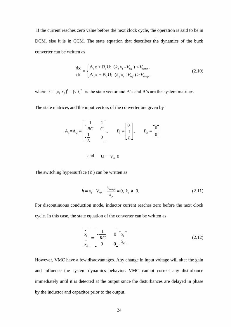
If the current reaches zero value before the next clock cycle, the operation is said to be in
DCM, else it is in CCM. The state equation that describes the dynamics of the buck
converter can be written as
1 1 1
2 2 1
A x + B U; ( - ) < ,dx=
A x + B U; ( - ) > .dt
p ref ramp
p ref ramp
k x V V
k x V V (2.10)
where 1 2[ ] [ ]x = = T Tx x v i is the state vector and A‟s and B‟s are the system matrices.
The state matrices and the input vectors of the converter are given by
1 2 1 2
1 10-
0A =A , , 1
01- 0
RC CB B
LL
and U 0inV
The switching hypersurface ( h ) can be written as
1 0, 0.
p
p
ramp
ref kk
vh x V (2.11)
For discontinuous conduction mode, inductor current reaches zero before the next clock
cycle. In this case, the state equation of the converter can be written as
1 1
22
1- 0
0 0
x xRC
xx
(2.12)
However, VMC have a few disadvantages. Any change in input voltage will alter the gain
and influence the system dynamics behavior. VMC cannot correct any disturbance
immediately until it is detected at the output since the disturbances are delayed in phase
by the inductor and capacitor prior to the output.

25
2.4.2 Current-mode Controlled Buck Converter
Another control scheme that is widely used for dc-dc converters is current mode
control. Current-mode controlled dc-dc converters usually have two feedback loops: a
current feedback loop and a voltage feedback loop. The inductor current is used as a
feedback state.
Figure 2.5: Current-mode controlled dc-dc buck converter
A current mode controlled dc-dc buck converter circuit is shown in figure.2.5. At the
beginning of a switching cycle, the clock signal sets the flip-flop ( 1q ), turning on the
(MOSFET) switch. The switch current, which is equal to the inductor current during this
interval, increases linearly. The inductor current Li is compared with the control signal
refi from the controller. When Li , is slightly greater than refi , the output of the comparator
goes high and resets the flip-flop ( 0q ), thereby turning off the switch. The switch will
be turned on again by the next clock signal and the same process repeated.
The buck converter circuit operates at continuous conduction mode. Depending on
the state of the switch, there are two circuit configurations, which are described by the
following differential equations:

26
0
0
is conducting
is blocking
-,
-,
inw
L
w
S
S
v v
di L
vdt
L
(2.13)
and
0
0
-L
vi
dv R
dt C (2.14)
If the switch position is expressed with the switching function q , then
1, closed
0, opened
w
w
Sq
S (2.15)
The control input signal is proportional to reference current refi . The reference current refi
is a function of output of the controller to regulate the output voltage.
The control voltage can be defined as,
1
0( )con p ref
vv k V
k for P controller
and 1 1
0 0- -con p ref I ref
v vv k V k V dt
k k, for PI controller.
Hence the reference current can be written as conref
f
vi
R, where fR is a proportionality
factor. The voltage waveforms are scaled to equivalent current waveforms by the
proportionality factor fR .
The state equation that describes the dynamics of the buck converter can be written as
1 1
2 2
A + B U; when is closed,=
A + B U; when is opened.
x Sdx
x Sdt (2.16)
where 1 2[ ] [ ]= = T Tx x v ix is the state vector and A‟s and B‟s are the system matrices.
The state matrices and the input vectors for the ON and OFF periods are

27
1 2 1 2
1 10-
0A =A , , 1
01- 0
RC CB B
LL
and U 0inv .
There are two types of current mode control strategies. In both, the switch is turned on at
the beginning of every clock period. In peak current mode control, the inductor current is
compared with a reference current signal with a compensation ramp, and the switch is
turned off when the two become equal. In the average current mode control, the inductor
current is compared with a ramp waveform, and the switch is tuned off when rampLi i . It is
turned on again at the next clock instant. Here a brief overview of peak current mode
control scheme is described.
2.4.2.1 Current Mode Control with Compensating Ramp
Figure 2.7 shows the waveform of inductor current of a switching converter
operating in continuous conduction mode (CCM). The inductor current changes with a
slope m1during the first subinterval, and a slope –m2 during the second subinterval. The
peak inductor current is controlled and the controlled method is therefore called peak
current-mode control. The current mode controller is unstable whenever the steady-state
duty cycle is greater than 0.5, resulting in sub-harmonic oscillation.
To avoid this stability problem, the control scheme is usually modified by adding an
external ramp to the sensed inductor current waveform. Let the slope of compensating
ramp is ma. when 2 0.5am m ,then the controller is stable for all duty cycles. The
relationship between the ramp, inductor and reference current is given in (2.12),
a S L S refi dT i dT i (2.17)

28
Then, the control equation is given by
0L ref a
S
ti i m
T (2.18)
Figure 2.6: Peak Current Mode Control
Figure 2.7: Inductor Current waveform with compensating ramp
Advantages of peak current mode control include Control of the peak inductor
current, inherent peak current limiting and sharing, good dynamic performance, first order
transfer function. Some of the main drawbacks of this control are the limited duty ratio,
increased output impedance, sub-harmonic oscillation, noise sensitivity. These problems
are rectified by means of an artificial ramp signal either subtracted from the control signal
or added to the inductor-current signal.

29
2.5 Sliding Mode Control for Dc-dc Buck Converter
Buck Converter is a time variable and a nonlinear switch circuit which possesses
variable structure features. Sliding mode control is well known for its good dynamic
response and stability due to its insensitive for parameters change and easier in
implementation, so this control technique is used extensively for the control of dc-dc
power converters [40], [41], [46]. This section explains about the implementation of a
hysteresis modulation (HM) based SM controller for dc-dc buck converter.
2.5.1 System Modeling
A typical SM controller for switching power converters has two control modes:
voltage mode and current mode. Here, voltage mode control is employed, i.e. output
voltage 0v , is the parameter to be controlled. Figure 2.8 shows the schematic diagram of a
SM voltage controlled buck converter. Here the state space description of the buck
converter under SM voltage control, where the control parameters are the output voltage
error and the voltage error dynamics is described.
Figure 2.8: Basic structure of an SMC buck converter system
30
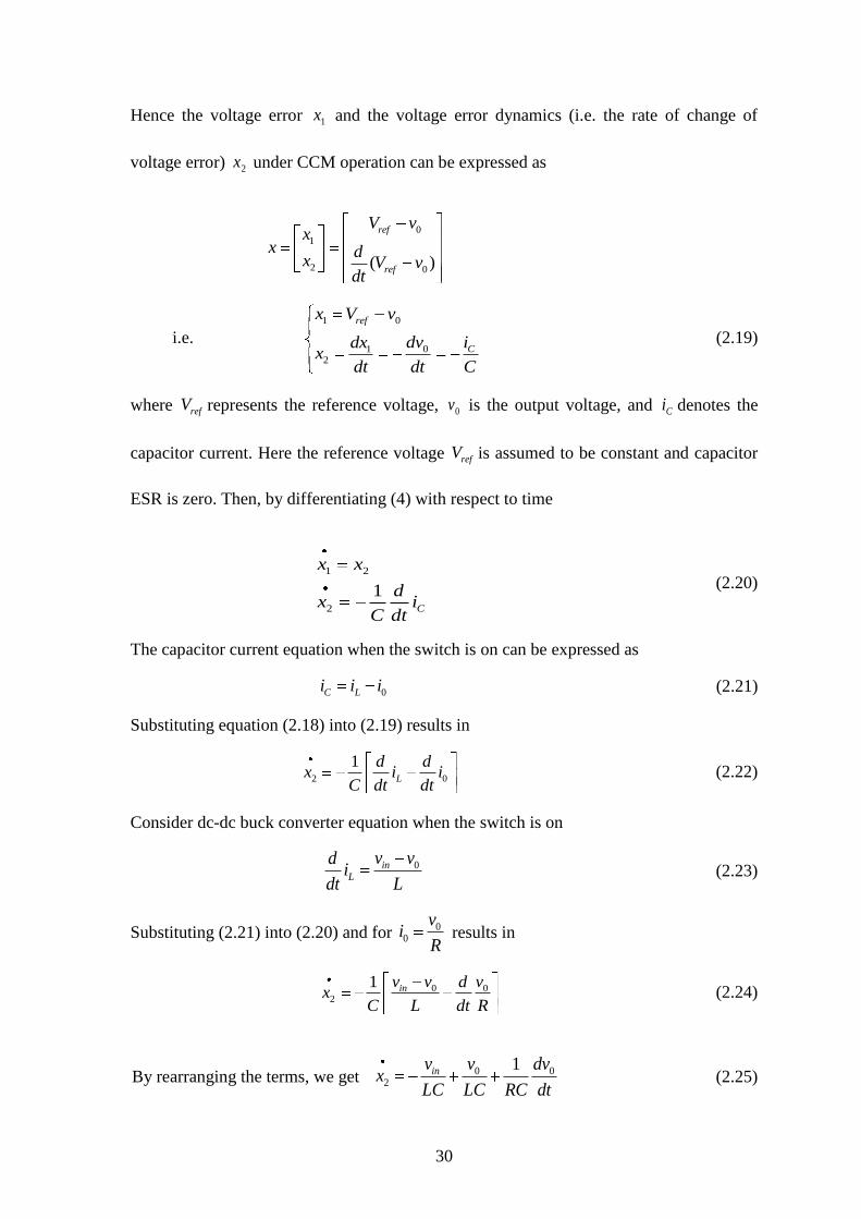
Hence the voltage error 1x and the voltage error dynamics (i.e. the rate of change of
voltage error) 2x under CCM operation can be expressed as
0
1
2 0
( )
ref
ref
V vx
x dx V v
dt
i.e. 1 0
012
ref
C
x V v
dv idxx
dt dt C
(2.19)
where refV represents the reference voltage, 0v is the output voltage, and Ci denotes the
capacitor current. Here the reference voltage refV is assumed to be constant and capacitor
ESR is zero. Then, by differentiating (4) with respect to time
1 2
2
1C
x x
dx i
C dt
(2.20)
The capacitor current equation when the switch is on can be expressed as
0C Li i i (2.21)
Substituting equation (2.18) into (2.19) results in
2 0
1L
d dx i i
C dt dt (2.22)
Consider dc-dc buck converter equation when the switch is on
0inL
v vdi
dt L (2.23)
Substituting (2.21) into (2.20) and for 00
vi
R results in
0 02
1 inv v vdx
C L dt R (2.24)
By rearranging the terms, we get 0 02
1inv v dvx
LC LC RC dt (2.25)
31
From equation (2.19), the output voltage, 0 1refv V x (2.26)
Substituting equation (2.24) into (2.23) leads to
1 22
refinVvx x
xLC RC LC LC
(2.27)
Hence, the system equations, in terms of state variables 1x and 2x can be written as
1 2
1 22
refin
x x
Vvx xx
LC RC LC LC
(2.28)
The state space model describing the system can be derived as
x Ax Bu D (2.29)
0 0 0 1
A , , D1 1- - refin
B Vv
LC RC LC LC
For DCM, inductor current is zero before the next clock cycle. This creates constraints to
the state variables. This can be derived by putting,
0Li . Hence, the equation of the can
be written as
2 1
1refx V x
RC (2.30)
The equation 2.12 represents a straight line in phase plane passing through points ( ,0)refV
and (0, )refV RC .
2.5.2 Design of SM Controller
In SM controller, the controller employs a sliding surface to decide its input states to
the system. For SM controller, the switching states u which corresponds the turning on
and off of the converter‟ switch is decided by sliding line. The sliding surface is described
as a linear combination of the state variables. Thus the switching function is chosen as
32
T
1 1 2 2 x 0S Cc x c x (2.31)
where T
1 2[ ],C c c is the vector of sliding surface coefficients and1 2
Tx xx . This
equation describes a sliding line in the phase plane passing through the origin, which
represents the stable operating point for this converter (zero output voltage error and its
derivative).
The sliding line acts as a boundary that splits the phase plane into two regions. Each of
this region is specified with a switching state to direct the phase trajectory toward the
sliding line. When the phase trajectory reaches and tracks the sliding line towards the
origin, then the system is considered to be stable, i.e., 1 0 x and 2 0x .
Substituting equation (2.20) into (2.31) results in
1 1 2 1 0S c x c x (2.32)
This describes the system dynamic in sliding mode. Thus, if existence and reaching
conditions of the sliding mode are satisfied, a stable system is obtained.
To ensure that a system follows its sliding surface, a control law is proposed. In this
system, the control law is defined as
1 ON when
0 OFF when
previous state, otherwise
S k
u S k (2.33)
where k is an arbitrarily small value. The reason for choosing S k and S k as the
switching boundary is to introduce a hysteresis band which determines the switching
frequency of the converter. If the parameters the state variables are such that S k , switch
wS of the buck converter will turn on. When S k , it will turn off. In the region
k S k , switch remains in its previous state.

33
Thus, this prevents the SM controller from operating at a high frequency for the power
switch to respond. It also alleviates the chattering effect which induces extremely high
frequency switching. The switching conditions in equation (2.33) are graphically shown
in figure 2.9.
Figure 2.9: Sliding line on 1 2x x phase plane
2.5.3 Derivation of SM Existence Condition
The control law in (2.33) only provides the information that the system trajectory is
driven toward the sliding line. In order to ensure that the trajectory is maintained on the
sliding line, the existence condition of SM operation, which is derived from Lyapunov‟s
second method to determine asymptotic stability, must be satisfied.
0
lim . 0S
S S (2.34)
Hence the specific conditions for the sliding regime to exist can also be expressed as
if
if
0, 0
0, 0
S S
S S
(2.35)
The existence condition can be expressed in the standard form
( )T TS C x C Ax Bu D (2.36)

34
Then the equation (2.32) in two circumstances, it gives,
0
0
0
0
TS
T T T
TS
T T
S C x
C Ax C B C D
S C x
C Ax C D
(2.37)
For buck converter, when 0S , the switch function 1q , and when 0S , the
switch function 0q . By substituting the matrices A, B, and D, and state variable x , the
above inequality becomes:
Case-I when 0 , 0S S
2 21 1 2 1 2 0
ref inV Vc cc x x c
RC LC LC (2.38)
Case-II when 0 , 0S S
2 22 1 2 1 2 0
refVc cc x x c
RC LC LC (2.39)
The equations 1 0 and 2 0 define two lines in the phase plane with the same slope
passing through points ,0refV and ,0ref inV v respectively. These two lines determine
the two boundaries of existence region from simulation these are clearly shown in figure
2.10. Point ,0ref inV v is the stable equilibrium point for the trajectories when the
switch is on. Similarly the trajectories corresponding to the system off state dynamic
always tries to converge to the point ,0refV , which is the off state equilibrium point. The
phase trajectory in SM operation is shown in figure 2.11. Sliding mode will occur on the
portion of the sliding line, 0S , that covers both the on state and off state region and it
will overshoot the sliding line if the phase trajectory present outside the existence region.
The value of system parameters and sliding coefficients are given in section 2.6. In figure

35
2.12, we have increased the value of sliding coefficients 1c to 5, so the overshoot is
increased and that changes the structure of the trajectory.
Figure 2.10: Region of existence of SM mapped in the phase plane
Figure 2.11: Evolution of phase trajectory in phase plane for 1 2RCc c

36
Figure 2.12: Phase plane diagram for 1 2RCc c
Figure 2.13: Phase plane diagram for 1 2RCc c
37
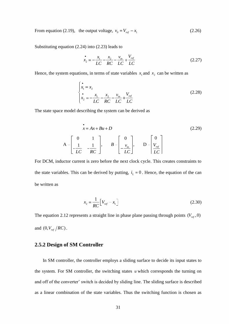
The chattering phenomenon can be defined as an undesirable oscillation around the
sliding surface at a high switching frequency due to the presence of switching
imperfections, parasitic effects etc. To control this undesirable high frequency oscillation,
generally a hysteresis band is imposed and the width hysteresis band determines the
switching frequency. The chattering phenomenon is illustrated in figure 2.14. From
figure, it is seen that narrower the hysteresis band higher the switching frequency and
except steady state operation, switching frequency is not constant.
Figure 2.14: Chattering Phenomena of SM control

38
2.6 Simulation Results and Discussions
In this section the simulation results are presented for comparison between the
different control methods that are discussed in above sections undergoing load current
step transient, input voltage step transient. The results of comparison are explained. There
are two different types of comparison study are presented. The first one is the
performance comparison between PWM based voltage-mode controlled buck converter
and HM based SM controlled buck converter. The second one is the performance
comparison between peak current-mode controlled buck converter with HM based SM
controlled buck converter.
The control methods have the same power circuit parameters and operate at the same
input and output voltages. The design specifications and the circuit parameters, for
simulation are chosen as: input voltage inv =20V, desired output voltage 0v =5V,
inductance L =3mH, capacitance C =69µF, and minimum load resistance minR =10Ω,
maximum load resistance maxR =15Ω, voltage reduction factor 1k =0.4, proportional gain
pk =2, and the upper and lower threshold of ramp voltage LV =3.8 and UV =8.2. The
sliding coefficients 1c =2 and 2c =0.001. The switching frequency Sf is set to 100 kHz.
2.5.1 PWM based Voltage-Mode Controller versus SM Controller
In this subsection, dynamic performance of PWM based voltage mode controlled
buck converter is compared with HM based SM controlled buck converter. The results
from simulation are given in figure 2.15-2.18. The transient responses of buck converter
employing PWM based voltage-mode control and SM control techniques are shown in
following figures respectively.

39
Figure 2.15: Output voltage response due to a step change in load resistance from 15Ω to
10Ω back to 15Ω
Figure 2.16: Inductor Current response due to a step change in load resistance from 15Ω
to 10Ω and back to 15 Ω

40
Figure 2.17: Output Voltage response for a change in input voltage from 20V to 15V and
back to 20V
Figure 2.18: Inductor Current response for a change in input voltage from 20V to 15V
and back to 20V
41
Figure 2.15 shows the output voltage waveform of the converter for a step change in
load resistance from 15Ω to 10Ω and then back to 15 Ω for both VMC and SM control.
The SM control Scheme takes 1.2ms settling time (time required to return to the steady
state) with an overshoot of 0.04volt as compared to 7ms and 0.5volt in case of the VMC.
Hence, SM control has a smaller overshoot and zero steady state error than VMC.
The inductor current response for a step load transient from 15Ω to 10Ω and then
back to 15 Ω for both VMC and SM control is then shown figure 2.16. From the result in
figure 2.16, we can see that the settling time is 0.04ms which is less compared to VMC
that has 7ms. This shows poor large-signal transient response due to the oscillatory nature
of the output voltage and the long settling time.
Similarly the system response for a change in input voltage from 20 volt to 15 volt
then back to 20 volt using both control schemes is shown in figure 2.17 and figure 2.18
respectively. From the results it is shown that the output of converter is not affected by
the input voltage variation in case of SM control where as the performance of converter
with VMC degrades having a long settling time and larger steady state error. This
demonstrates the advantage SM controller over VMC for providing faster transient
response for a wide operating range.
2.5.2 Peak-Current-Mode Controller versus SM Controller
In this subsection, the dynamic performance of Peak-Current-mode controlled buck
converter is compared with HM based SM controlled buck converter. The comparison
results are shown in the following figures. The transient responses of buck converter
employing PWM based peak-current-mode control and SM control techniques are shown
in the following figures respectively.

42
Figure 2.19: Output Voltage response with step load transient from 15Ω to 10Ω and then
back to 15 Ω
Figure 2.20: Inductor Current response with step load transient from 15Ω to 10Ω and
then back to 15 Ω

43
Figure 2.21: Output Voltage response for a change in input voltage from 20V to 15V
and back to 20V
Figure 2.22: Inductor Current response for a change in input voltage from 20V to 15V
and back to 20V

44
From the above figures (figure 2.19 to figure 2.22), it is seen that the transient response
corresponding to SM controller is faster and has smaller overshoot when compared to the
transient responses in PCMC. PCMC is usually faster than VMC because of its additional
inner current control loop and compensation technique used for PCMC is lesser complex
than VMC. Also the transient response of PCMC is faster than VMC. But, when the
PCMC method is compared with the SM controller, again SM control method is proved
to be better solution for its robustness to line and load variations.
The transient response of SM controlled buck converter can be understood from phase
plane analysis method. The phase plane plot of SM control for a step change in load from
15Ω to 10Ω and then back to 15Ω is shown in figure 2.23. From figure we can see that
the phase trajectory starting from any initial position always tries to settle at the stable
equilibrium point (origin) and when the load changes the trajectory located at some other
initial position again tracks the sliding line by reaching back to origin.
Figure 2.23: Phase plane plot under step load transient for SM control

45
2.7 Conclusion
The different control methods for dc-dc buck converter are discussed. The simulation
results are also presented. The results of comparison are explained. The dynamic results
in order to validate the disturbance rejection in larger range of variations are presented.
The SM control method shows better dynamics for changes in input voltage and load
compared to the PWM voltage-mode and current-mode control methods. It can be seen
that the SM control method can well regulate the output voltage even in large range of
load and line variation.


46
CHAPTER 3
Fixed Frequency Hysteresis Control
3.1 Introduction
The use of hysteretic controllers for low voltage regulators used in computer and
communication systems has been gaining interest due its various advantages. Advantages
of this control approach includes fast response and robust with simple design and
implementation. They do not require components for feedback loop compensation [6]-[8].
This reduces the number of components and size of theoretical analysis for
implementation and also reduces the design effort for calculating the circuit component
values (like inductor, capacitor, and input voltage). They response to disturbances and
load change right after the transient takes place. Hence they give excellent transient
performances. While the elimination of the compensation network allows for fast
responses to transient, the hysteresis controlled converter suffers from two major
drawbacks: variable switching frequency and non zero steady-state error. Non zero
steady-state error may be rectified by adding a PI block in series with the voltage
feedback. Also, the output voltage ripple is higher than the fixed band of hysteresis
comparator. That is because of delays and output filter parasitic element. The application
of nonlinear control theory can be used for study and analysis of hysteretic controlled
converters for alleviating the above mentioned problems. This way of analysis gives a
better idea for proper design method [6].

47
3.2 Variable Frequency Hysteretic Controllers
In this section, the basic ideas about the hysteretic controlled converters with variable
switching frequency are described. As shown in Figure 3.1, the voltage hysteretic
controller regulates the output voltage ripple within the hysteretic band. Similarly, a
current hysteretic controller directly regulates the inductor current of the converter by
regulating the inductor ripple or a scaled version of it within the hysteretic band.
Figure 3.1: voltage hysteresis control
3.2.1 Hysteretic Voltage-Mode Controller
Hysteretic voltage-mode control is the simplest control method available. The
concept of operation is very simple. The switch is turned on, when the output voltage falls
below minimum set point (i.e., lower boundary) and turns off when output voltage is
higher than maximum set point (i.e., upper boundary). Since the controller does not use a
compensation network, the converter is able to react quickly to a transient event making it
seem like a perfect solution for voltage regulator modules. However, the drawback of the
voltage-mode hysteretic controller is its reliance on the converter‟s output capacitor
parasitic. A block diagram of voltage hysteretic controlled converter is illustrated in
Figure 3.1.

48
3.2.2 Hysteretic Current-Mode Controller
Hysteretic current-mode control functions by controlling both the peak inductor
current and the valley inductor current. It does not require an external oscillator or saw-
tooth generator for operation and it has the ability to provide a fast response to a transient
event. Figure 3.2 illustrates a block diagram of a current-mode hysteretic controlled dc-dc
converter.
Figure 3.2: Hysteretic CM controlled buck converter
The power converter circuit with feedback control generally consists of:
1. a power stage with switches wS and D , and storage elements L and C ,
2. an inner controller preserving the converter‟s working principle by switching the
circuit topology,
3. an outer controller adjusting the inner loop‟s reference in response to deviations from
the desired output.
The control system shown in figure 3.2 consists of two control loops. One is the
current control loop and the other is the voltage control loop. The error between the actual
output voltage and reference voltage gives the error voltage. A P or PI control block can
use the voltage error signal to provide a reference current for hysteresis control. Hence
the current hysteretic control method can be viewed as a sliding mode control system.

49
The hysteretic comparator implements the control law i.e.
1, 0
0, 0
Su
S (3.1)
where, S is the sliding surface, which is defined as the difference between the two
comparator inputs.
0( )p ref LS K v v k i (3.2)
where k is the current sensing gain which has a fixed value and pK is proportional gain as
we consider a proportional controller here. From the previous chapter, we know that the
buck converter power circuit is described by two sets of differential equations that are,
0 Lin
diL v v
dt and 0c
L
dv vC i
dt R (3.3)
Let the two state variable of the control system are 1 0refx V v and 2 Lx i , then by
taking the derivative,
2 1
2 1
1
in ref
refin
L x v v x
vvx x
L L L
(3.4)
and
1
2 1
2 11
ref
ref
v xx C x
R
vx xx
C RC RC
(3.5)
The state space model in terms of state variables is given by,
1 1A x + B +D; ux (3.6)
11
22
1 100-
1- 0
refin
xx
RC Cu vv
x x L LL
(3.7)
50
where „u‟ is a discontinuous input that is either 0 or 1. The sliding dynamics of the system
are obtained by using the equivalent control method [12]. The discrete form of the control
input u is substituted with a continuous function equ . The dynamics of the closed loop
system, assuming that an ideal sliding motion (infinite switching frequency) exists on the
switching surface, „ S ‟, is governed by the conditions,
1
• •
0 0
.
ni
i i
S S
dxds S
dt x dt
dsS x G x
dt
(3.8)
where G is a 1 by n matrix and the above equation is given as,
1 1 1( ) 0eqG x A x B u D
The equivalent continuous control input equ can be written as,
1
1 1 1
1
1 1 1 1 1 1
1
1 1 1 1
( ) ( )
( ) ( )
[ - ( ) ]( )
equ GB G A x D
x A x D B GB G A x D
x I B GB G A x D
(3.9)
This equation describes motion equation of the converter when operating in SM
operation.
3.3 Simulation Results
The simulation results are shown below derived for a current hysteresis controlled
dc-dc buck converter with the same power circuit parameters that we have taken earlier in
chapter 2. The effectiveness of hysteretic controlled converters is demonstrated through
the results. Figure 3.3 shows the transient performance for step change in load from 15Ω
to 10Ω and back to 15Ω. Figure 3.4 shows the transient response for input voltage
variation from 20V to 15Vand back to 20V.

51
Figure 3.3: Transient response of the hysteretic current controlled buck converter when
load changes from 15Ω to 10Ω and back 10Ω

52
Figure 3.4: Transient response of the hysteretic current controlled buck converter when
input voltage changes from 25V to 15V and back to 25V

53
From the results, it is seen that current hysteretic controller quickly responds to
disturbances for large line and load variation. For a input voltage transient response, the
current hysteretic controller has a negligible steady state error.
Phase plane analysis using the phase portrait is a very good graphical tool for
analyzing the behavior of fast transient hysteretic control. This analysis is suitable for
large signal analysis. By phase plane analysis method, the transient response is better
understood and is shown in figure 3.5.
Figure 3.5: Phase portrait with load transient
In steady state the phase trajectory is on the stable equilibrium point. When transient
occurs, the equilibrium is broken and the phase trajectory will direct towards a new
equilibrium point and settles there again by making limit cycle.

54
3.4 Constant Switching Frequency Current-mode Hysteretic
Controller
As discussed in previous chapter, different control techniques are used for
controlling dc-dc converters. Some of the conventional control techniques are also
described in previous chapter. In this section, a new control topology, which includes the
concept of SM control and peak current mode control is proposed. Therefore the essential
tools of the nonlinear control theory can be introduced for the study of this hysteresis
controller. The proposed control scheme is actually a fixed frequency hysteretic current
mode controller for dc-dc buck converter that operates in pseudo-CCM (PCCM) [64],
[65]. In PCCM operation, the conventional buck converter circuit is modified by
connecting an extra of switch across the inductor. This divides the total switching cycle
into three subintervals which is termed as PCCM. The converter with this additional third
interval is also known as tristate converter. Thus, the new control approach provides the
advantages that are simple in implementation, fixed switching frequency operation, good
transient performances and does not require a compensating ramp signal.
3.4.1 Basic Concept of Operation
The operation of the tristate dc-dc buck converter with hysteretic current-mode
control scheme is discussed in this subsection. Figure 3.6 shows the tristate buck
converter topology. It consists of two controlled switches 1S and 2S , an uncontrolled
switch D , an inductor L and a capacitor C , a load resistance R . Switch 2S is the
additional switch which is connected across the inductor. The operation of the tristate
converter includes three different configuration or structures that are show in figure 3.7.
At the start of the clock period, the switch 1S is turned on and the switch 2S is turned off.
During this interval (mode 1), inductor current increases with a slope of 0inv v
L.

55
When Li reaches a peak value (upper bound), 1S turns off. Then, Li starts falling with a
slope of 0v
Luntil it reaches some lower threshold. This interval is denoted as mode 2.
During this interval, diode is forward biased and both switch 1S and 2S are turned off.
When the inductor current reaches lower threshold, it stays constant at lower boundary,
because the switch 2S shorts the inductor L and voltage across the voltage across the
inductor is thus equal to zero. During this interval 2S is turned on while 1S and diode are
off. This is the additional interval, denoted as mode 3.The inductor current waveform
showing the switch conditions for a tristate buck converter is shown in figure 3.8. All the
circuit components are assumed to be ideal in the derivations.
Figure 3.6: A tristate buck converter configuration
(a) (b)

56
(c)
Figure 3.7: Equivalent circuits under different modes of operation: (a) mode 1 ( 1 SD T ), (b)
mode 2 ( 2 SD T ), and (c) mode 3 ( 3 SD T ).
These three modes of operation can be described as follows:
Mode 1: when 1S is on and, 2S is off, the state space equation of buck converter is derived
as
1 10
11
0
in
dx RC Cx v
dtL
L
(3.10)
where 0[ ]T
Lx v i , 0v is the output voltage, Li is the inductor current.
Mode 2: when 1S and 2S both are off, the equation is derived as,
1 1
0
01 0
in
dx RC Cx v
dt
L
(3.11)
Mode 3: when 1S is off, and 2S is on, the state-space equation is
10 0
0
0 0in
dxx vRC
dt (3.12)

57
Figure 3.8: Inductor current waveform of tristate buck converter showing the switch
conditions
3.4.2 Mathematical Analysis of Proposed Controller
The operation of a hysteretic current-mode controller for tristate dc-dc buck converter is
proposed and the schematic diagram of proposed controller is shown figure 3.9.
Figure 3.9: Schematic diagram of the hysteretic controller for tristate buck converter

58
The digital logic blocks generates required switching pulses for controlling the
switches 1S and 2S . This block consists of two SR flip-fops and some logic gates that can
be shown in figure 3.10.
Figure 3.10: Schematic diagram of pulse generator circuit
The state-space description of the system in terms of the desired control variables (i.e.,
voltage, current etc) is developed. The proposed current controller employs both the
output voltage error 1x and the inductor current 2x as the controlled state variables, which
are expressed as
1 0
2
ref
L
x v v
x i (3.13)
where Li represent the inductor current, 0v and refv represent the output voltage and
reference voltage respectively. Here the switching state of the switch is either 1 or 0.
Then by taking the derivative of (3.13) with respect to time,
01
2L
dvx
dt
dix
dt
(3.14)
Considering the buck converter when the switch 1S is on, 2S off
0L
in
diL v v
dt (3.15)

59
0cL
dv vi C
dt R (3.16)
Substituting equation (3.14) into equation (3.15) and (3.16) results in
1 1 2
2 1
1 1
1
ref
refin
vx x x
RC C RC
vvx x
L L L
(3.17)
The dynamics of the converter circuit, when 1S and 2S are off, can be expressed as,
0Ldi
L vdt
(3.18)
0cL
dv vi C
dt R (3.19)
Substituting equation (3.14) into equation (3.18) and (3.19) results in
1 1 2
2 1
1 1
1
ref
ref
vx x x
RC C RC
vx x
L L
(3.20)
The dynamics of the converter circuit in mode 3, when 2S is on, 1S is off, can be
expressed as,
0LdiL
dt (3.21)
0cL
dv vi C
dt R (3.22)
Since in this mode of operation, inductor current stays at a constant value, so we get the
derivative of a constant value is zero. By substituting equation (3.14) into equation (3.21)
and (3.22) results in,
1 1
2
1
0
x xRC
x
(3.23)

60
Then, the state-space modeling of the converter circuit with state variables 1x and 2x is
given by,
1 1 1 1 2
2 2 2 1 2
3 3 3 1 2
A x + B +D ; when is on,and is offx
A x + B +D ; when both and are off
A x + B +D ; when is off , and is on
S Sd
S Sdt
S S
(3.24)
where 1 2x = [ ]Tx x is the state vector and A‟s and B‟s are the system matrices.
The state matrices and the input vectors for the three periods are,
1 2 3
1 2 1 2 3
1 11 - -
- 0A A , A ,
1 0 0 0
11 0
0B , B , D D , D
0 1 0
refin
RC CRC
L
RCV RCV
LL
As studied from the previous discussion that the basic principles of a hysteresis control
is based on the two hysteresis bands (upper and lower bands), whereby the controller
turns the switch on when the output current falls below the lower band and turns the
switch off when output is beyond the upper bound. The switching action can be
determined in the following way,
1. If Li < lower bound, (ON)1 u
2. If Li > upper bound, (OFF)0 u , where u is the control input.
In this case, the hysteretic current controller shown in figure 3.2 consists of two
control loops. One is the current control loop and the other is the voltage control loop.
The difference between the actual output voltage and reference voltage generates the error
voltage. A controller may a P or PI type use the voltage error signal to provide a control

61
voltage which is consider as the upper boundary or the upper threshold hysv . Here a
simple proportional controller is considered for easy analysis. The control voltage conv is
a function of the output voltage 0v and a reference signal ref
V in the form,
0( )con p ref
v k V v (3.25)
where, pk is the gain of proportional controller. The lower threshold hysv , is determined
by subtracting a small constant term , which is given as, hys hysv v . Hence, there
are two switching actions 1u and 2u are occurring on the two switching surfaces in the
region of phase plane. The control law determines the switching action. This can be
represented mathematically as,
1
1
1
when and
when and
1, 0
0, 0
L
L
hys
hys
k h
k h
i vu
i v
(3.26)
2
2
when and
otherwise
1, 0
0,
L hysk hi vu
(3.27)
where 1h and 2h are the two switching surfaces (manifolds) in sliding mode phase plane
that can be expressed as the combination of state variables,
1 1 2 1
2 1 2 2
c
c
T
p
T
p
h k x kx x
h k x kx x (3.28)
where 1x and 2x are the state variables, k is a constant factor that transforms the current
signal to voltage signal, pk is the proportional gain, which is known as sliding coefficient.
In the equations (3.26) and (3.27), 1u and 2u can be known as the discrete control inputs
to the system and this equations forms the basis of control law for the hysteretic control
system.

62
Generally a SM control design approach consists of two components. The first involves
the design of a sliding surface and the second is concerned with the selection of a control
law that directs the system trajectory towards system stable operating point. If we assume
the width of the hysteresis band 0 , then there exists only a single switching surface
1h in phase plane. And for sliding mode to be exist on the switching surface, then 1 0h .
This is said to be as ideal SM operation. Hence for ideal SM operation 1 1 0dh dt h .
Also the equivalent control produces trajectory whose motion is exactly equivalent to the
trajectory‟s motion in an ideal SM operation [15]. In equivalent control, the discrete
control input is substituted by continuous equivalent control signal equ and is obtained by
solving the equations,
1 1
1
1 1 1 1
1
1 1 1 1 1
0
0
( ) 0
[ ] [ ]
T
T
eq
T T
eq
dh dt h
c x
c A x B u D
u c B c A x D
(3.29)
Then substituting the values, we get
1
1 1
2
1 1 1 2
1 1 - -
[ - ]1
0
T
p
p pT
xRC Cc A x k k
x
L
k kkc A x x x
RC L C
(3.30)
1 1
1 1
0
[ - ]T
p in
T in
c B k k v
L
vc B k
L
(3.31)

63
1 1
1 1
1
[ - ]1
T
p ref
p ref refT
RCc D k k V
L
k V kVc D
RC L
(3.32)
1 1 1 1
1 2
( ) 0
0
T
eq
p p p ref refineq
c A x B u D
k k k V kVkvkx x u
RC L C L RC L
(3.33)
From above equation (3.33), equ can be found as
0 p p p ref ref
eq ref L
in in in in
k k L k LV VL ku V v i
kv RC L Ckv RCkv v (3.34)
where equ is a smooth function of the discrete input functionu and bounded by 0 and 1.
Then by substituting (3.21) into 0 1equ , the function can be expressed as,
00 1p p p ref ref
ref L
in in in in
k k L k LV VL kv v i
kv RC L Ckv RCkv v (3.35)
Multiplying the above equation by inv ,
0
10
p p p
ref L ref in
k k L k LLv v i V v
k RC L Ck RCk (3.36)
The SM existence region provides a range of sliding area where the sliding motion takes
place. The condition for the existence of sliding mode is achieved, if the following
inequalities are satisfied.
1
1
10
10
1
1
lim 0
lim 0
h
h
h h
h h
(3.37)
For 1 1 0 , 0h h : 1 1 1 1 1 c (A x + B +D )<0Th (3.38)
For 1 1 0 , 0h h : 1 1 1 1 1 c (A x + B +D )>0Th (3.39)

64
By solving the above equations, we get,
L1: 1 2 0p p p ref ref in
k k k v kv kvkx x
RC L C RC L L for 1 0h (3.40)
L2: 1 2 0p p p ref refk k k v kvk
x xRC L C RC L
for 1 0h (3.41)
The above two equations represents two lines in phase plane with same slope. As there
are two switching surfaces, so the SM existence region for hysteresis controlled
converters can be found out by considering both the switching surfaces for analysis. From
these equations we can find out the values of control parameters such that it will satisfy
the existence condition.
3.5 Model including parasitic elements
The influence of parasitic elements on the converter behavior is not yet discussed.
Therefore the circuit including the parasitic elements is given below. The tristate buck
converter circuit consists of parasitic elements in the switches ( 1r and 2r ), the capacitor
( cr ), the inductor ( Lr ) , and the diode ( )dr , are shown in figure 3.11.
Figure 3.11: Model of tristate buck converter with all parasitic elements
65
The three modes of operation can be described as follows:
Mode 1: when 1S is on and 2S is off, the state space equation of buck converter is
derived as
1
1 0( ) ( )
11
( ) ( ) ( )
c c
in
cL
c c
R
C R r C R rdxx v
dt RrRr r L
L R r L R r
(3.42)
where [ ]T
c Lx v i , Li is the inductor current, cv is the output voltage.
Mode 2: when 1S and, 2S both are off, the equation is derived as,
1
( ) ( ) 0
01 ( )
( ) ( )
c c
in
cd L
c c
R
C R r C R rdxx v
dt RrRr r
L R r L R r
(3.43)
Mode 3: when 1S is off, and 2S is on, the state-space equation is
2
1 0
0( )
0 0 -
cin
L
C R rdxx v
dt r r
L
(3.44)
3.6 Simulation Results
In this subsection, based on the above proposed hysteretic current control method, the
simulation studies have been performed on a dc-dc buck converter under steady-state and
also under dynamic conditions of line and load variations. The buck converter parameters
chosen for the simulation studies are input voltage inv =20V, desired output voltage 0v
=5V, inductance L =3mH, capacitance C =69µF, minimum load resistance minR =10Ω,
maximum load resistance maxR =15Ω, voltage reduction factor 1k =0.8, proportional gain

66
pk =2, delta = 0.03, and current sensing gain k =3Ω.The switching frequency Sf is set
to 100 kHz. A simple proportional controller is considered here. The simulations are done
using MATLAB/SIMULINK.
Figure 3.12: Start-up transient performance of the converter with the proposed controller
The current hysteretic control converter operated in PCCM operation showed less
current and voltage ripple. From the results, we got the value of output voltage ripple and
inductor current ripple as 0.005 V and 0.012A in steady state.

67
Figure 3.13: The proposed current hysteretic controller operating principle

68
Figure 3.14: Transient response for change in load from 15Ω to 10Ω and back to 15Ω
Figure 3.15: Output voltage response from load transient 10Ω to 15Ω

69
Figure 3.16: Load transient response from 15Ω to 10Ω
Figure 3.17: Load transient response from 15Ω to 10Ω for conventional current hysteretic
control method
From figure 3.16 and 3.17, it is seen that in case conventional current hysteretic control
method the switching frequency is not constant (1 2
T T ) when load is varied. But for the
proposed control technique we are getting a fixed switching frequency ( 1 2
T T ) when
load varies.

70
Figure 3.18: Transient response due to a step change in reference voltage from 6V to5V
and back to 6 V

71
Figure 3.19 shows the motion of the phase trajectory in two dimensional plane. In this
case three states exist on phase plane. When the phase trajectory hits the lower boundary,
system status changes to first sub circuit state. When it touches the upper boundary,
system status changes to second sub circuit state and again when it touches the lower
boundary, system status changes to third sub circuit state for a fixed period. With these
switching actions, the trajectory slide within the hysteretic band towards the system
steady state operating point and makes a limit cycle around that point. Hence, the states
are regulated in one operating point by means of control law.
Figure 3.19: phase plane diagram
Figure 3.20: Magnified view showing the phase trajectory and hysteresis band

72
The simulation results for the buck converter with the proposed current hysteretic
controller including all the parasitic elements are shown in following figures. The values
of the resistive parasitic components are chosen as: 1r =2.1 mΩ, 2r = 0.2 Ω, cr =5.5 mΩ,
Lr =0.8 Ω, dr =2.1 mΩ respectively.
Figure 3.21: The output voltage ripple and inductor current ripple in steady state
operation by considering the effect of parasitic elements

73
To increase the duration of mode 3 the level of lower boundary must be increased.
Therefore to increase the level of lower lower boundary that is hys hysv v , the
value of is decreased. So value is taken as 0.02. The inductor current ripple in steady
state operation is shown in figure 3.22 that shows the longer duration for mode 3.
Figure 3.22: The inductor current ripple in steady state operation

74
3.7 Conclusion
In this chapter, the principle and operation of different types of hysteresis controllers are
discussed. The effectiveness of hysteretic controller for faster transient response is
described through the simulation results. The main problem associated with these
conventional hysteretic controlled converters is variable switching frequency operation.
Thus a constant switching frequency hysteretic controller is proposed. The controller is of
current-mode operation. The proposed controller is simple in design and implementation
without the use of compensating ramp circuit. The steady state and transient responses are
presented. The result shows good performances.


75
CHAPTER 4
Conclusions
4.1 Conclusions
This chapter summarizes the contributions and the main results of the thesis. The thesis
has explained about the merits and demerits of different control methods such as the
PWM voltage mode control, peak current mode control, hysteresis control and sliding
mode control for dc-dc buck converter. A fixed frequency current hysteresis control has
been designed for buck converter.
Chapter 1 describes the importance and application of switch mode dc-dc converter. The
various control schemes used for dc-dc converters has been explained in brief. A review
study on the previous work in this area has been presented. The main frame of the work
and also the work done in each chapter has been described.
In chapter 2 a detailed explanation and classification of existing control techniques for
switched mode power supplies have been given. The chapter also defined and
summarized, with the aid of mathematical equations for dc-dc buck converter. The
information about the different modes of operations that are continuous conduction mode
(CCM), discontinuous conduction mode (DCM) has been given. A comparison study has
been carried out for studying the effects of PWM controllers and SM control on the dc-dc
buck converter response in steady state, under line variations, load variations, and
different component variations.

76
Chapter 3 gives a detail study on hysteretic control dc-dc converters. The advantages and
drawbacks of main types of hysteretic controllers i.e. voltage hysteresis control and
current hysteresis control has been explained. The principle of operation of tristate buck
converter was given. A hysteretic current control technique for a tri-state buck converter
operating in constant switching frequency has been designed and behavior of the
controller is studied by using sliding mode control theory because dc-dc buck converter is
a variable structure system due to the presence of switching actions. The converter
response has been investigated in the steady-state region and in the dynamic region.
The main work of this thesis can be summarized as follows:
Study of the PWM voltage mode control, PWM current mode control and their
operation has been given. The advantages and drawbacks of each control method
when implemented in switched-mode power converters are shown.
The analysis and the theories of SM control were given in details. SM control
implemented in dc-dc buck converter is presented. Then a comparative analysis on
conventional PWM controllers and SM control has been done. The simulated result
showed the satisfying theories of SM control. The advantages of SM control over
other control methods are described.
The basic concept of operation of tristate buck converter has been studied. The
implementation of fixed frequency hysteretic current control to the tristate buck
converter has been given. The output voltage, main inductor current waveforms
were studied in steady-state region and in dynamic region.

77
4.2 Scope of Future Work
Following are the areas of future study which can be considered for further research
work.
The proposed control method is applied on dc-dc buck converter. It can be applied
to many other converter topologies. The non zero steady state error is minimized
by adding PI block in the feedback control loop.
The using the sliding mode control concept used for studying the behavior of
hysteretic controlled dc-dc buck converter can be extended for other converter
topologies.
To verify the theoretical study, the proposed control scheme can be done with
experimental prototype.


78
References
[1] M. H. Rashid, Power Electronics: Circuits, Devices and Applications (3rd Edition),
Prentice Hall, 2003.
[2] N. Mohan , T. M. Undeland, W. P. Robbins, Power Electronics: Converters,
Applications, and Design, 3rd Bk&Cdr edition, Wiley, 2002.
[3] R.D Middlebrook and S Cuk , “A general unified approach to modeling switching
Converter Power stages,” in Proc. IEEE PESC Rec., pp. 18–34, 1976.
[4] A.J. Forsyth and S.V. Mollow, “Modeling and control of dc-dc converters,” IEE power
engineering journal, vol. 12, no. 5, pp. 229–236, Oct. 1998.
[5] V.S.C Raviraj and P.C. Sen, “Comparative Study of proportional-integral, Sliding-mode,
and fuzzy logic controllers for power converters,” IEEE transaction on Industry
applications, vol. 33, no. 2, pp. 518-524, Mar. /Apr. 1997.
[6] M. Castilla, L. G. de Vicuna, J.M. Guerrero, J. Matas, and J. Miret, „Design of voltage-
mode hysteretic controllers for synchronous buck converters supplying microprocessor
loads‟, IEE Proceedings on Electrical Power Applications, Vol.152, No. 5, pp.1171–
1178, Sep. 2005.
[7] M. Castilla, L. G. de Vicuna, J.M. Guerrero, J. Miret, and N. Berbel, „Simple low-cost
hysteretic controller for single-phase synchronous buck converter‟, IEEE Transactions
on Power Electronics, Vol. 22, No. 4, pp.1232–1241, Jul. 2007.
[8] M. Castilla, L. G. de Vicuna, J.M. Guerrero, J. Matas, and J. Miret, „Designing VRM
hysteretic controllers for optimal transient response‟, IEEE Transactions on Industrial
Electronics, Vol. 54, No. 3, pp.1726–1738, Jun. 2007.

79
[9] T. Nabeshima, T. Sato, S. Yoshida, S. Chiba, and K. Onda, “Analysis and design
considerations of a buck converter with a hysteretic PWM controller,” in Proc. IEEE
PESC, pp. 1711–1716, 2004.
[10] V. Utkin, J. Guldner, and J. X. Shi, Sliding Mode Control in Electromechanical Systems.
London, U.K.: Taylor & Francis, 1999.
[11] C. Edwards and S. K. Spurgeron, Sliding Mode Control: Theory and Applications.
London, U.K.: Taylor & Francis, 1998.
[12] R. Venkataramanan, “Sliding mode control of power converters,” Ph.D. dissertation,
California Inst. Technol., Dept. Elect. Eng., Pasadena, CA, May 1986.
[13] F. Bilalovic, O. Music and A. Sabanovic, “Buck converter regulator operating in siding
mode,” in Proc. 7th
Int. Conf.PCI, pp. 331-340, Apr. 1983.
[14] R. Venkatramanan, A. Sabanovic, and S. Cuk, “Sliding mode control of DC-to-DC
converters,” in Proc. IEEE Conf. IECON, pp. 251-258, 1985.
[15] S. C. Tan, Y. M. Lai, C. K. Tse, “General design issues of sliding-mode controllers in
dc-dc converters,” IEEE Trans. Industrial Electronics., vol. 55, no. 3, pp. 1160–1174,
Mar. 2008.
[16] S.P Huang, H.Q. Xu, and Y.F. Liu. L, “Sliding mode controlled Cuk switching regulator
with fast response and first-order dynamic characteristics,” in Proc. IEEE PESC Rec.,
pp. 124-129, Jun. 1989.
[17] E. Fossas, L. Martinez, and j. Ordinas, “Sliding-mode control reduces audio
susceptibility and load perturbation in the Cuk converter,” IEEE Trans. Circuits Syst. I.
Fundam. Theory Appl., vol. 39, no. 10, pp. 847-849, Oct. 1992.
[18] L. Malesani, L. Rossetto, G. Spiazzi, and P. Tenti, “Performance optimization of Cuk
converters by sliding-mode control,” IEEE Trans. Power Electron., vol. 10, no. 3, pp.
302-309, May 1995.

80
[19] M. Oppenheimer, M. Husain, M. Elbuluk, and J. A. De Abreu Garcia, “Sliding mode
control of cuk converter,” in Proc. IEEE PESC Rec., vol. 2, pp. 1519-1526, Jun. 1996.
[20] J. Mahadavi and A. Emadi, “Sliding-mode control of PWM Cuk converter,” in Proc.6th
Int. Conf. Power Electron. Variable Speed Drives, vol. 2, pp. 372-377, Sep.1996.
[21] E. Fossas and A. Pas , “Second order sliding mode control of a buck converter,” in Proc.
41st IEEE Conf. Decision Control, vol. 1, pp. 346-347, Dec. 2002.
[22] Y. B. Shtessel, A. S. I. Zinober, and I. A. Shkolnikov, “Boost and buck-boost power
converters control via sliding modes using method of stable system centre,” in Proc. 41st
IEEE Conf. Decision Control, vol. 1, pp. 346-347, Dec. 2002.
[23] Y. B. Shtessel, A. S. I. Zinober, and I. A. Shkolnikov, “Boost and buck-boost power
converters control via sliding modes using dynamic sliding manifold,” in Proc. 41st
IEEE Conf. Decision Control, vol. 3, pp. 2456-2461, Dec. 2002.
[24] H.Sira-Ramirez , “Sliding mode-∆ modulation control of a “buck converter”,” in proc.
42end IEEE Conf. Decision control, vol. 3, pp. 2999-3004, Dec. 2003.
[25] H. Sira-Ramirez, “On the generalized PI sliding mode control of DC-TO-DC power
converters: A tutorial,” Int.J. Control, vol. 76, no. 9/10, pp. 1018-1033, 2003.
[26] V. S. C. Raviraj and P. C. Sen, “Comparative study of proportional integral, sliding
mode, and fuzzy logic controllers for power converters,” IEEE Trans. Ind. Appl., vol. 33,
no. 2, pp. 518–524, Mar./Apr. 1997.
[27] P. F. Donoso-Garcia, P. C. Cortizo, B. R. de Menez, and M. A. Severo Mendes, Sliding
mode control for current distribution in DC-to-DC converters connected in parallel,” in
proc. IEEE PESC Rec., pp. 1513-1518, Jun. 1996.
[28] Y. B. Shtessel, O. A. Raznopolov, and L. A. Ozerov, “Sliding mode control of multiple
modular DC-to-DC power converters,” in Proc. IEEE Int. Conf. Control Appl., pp. 685-
690, Dec. 1996.

81
[29] H. Sira-Ramirez and M. Rios-Bolivar, “Sliding mode control of DC-to-DC power
converters via extended linearization,” IEEE Trans. Circuit Syst. I, Fundum Theory
Appl., vol. 41, no. 1, pp. 652-651, Oct. 1994.
[30] H. Sira-Ramirez, R. Ortega, R. Perez-Moreno, and M. Garcia-Esteban, “A sliding mode
controller-observer for DC-to-DC power converters: A passivity approach,” in Proc. 34th
IEEE Conf. Decision Control, pp. 3379-3784, Dec.1995.
[31] H. Sira-Ramirez, G. Escobar, and R. Ortega, “On passivity-based sliding mode control
of switched DC-to-DC power converters,” in Proc. 35th
IEEE Conf. Decision Control,
pp. 2525-2526, Dec.1996.
[32] J. M. Carrasco, J. M. Quero, F. P. Ridao, M. A. Perales and L. G. Fanquelo, “Sliding
mode control of a DC/DC PWM converter with PFC implemented by neural networks,”
IEEE Trans. Circuits Syst. I, Fundam, Theory Appl., vol. 44, no. 8, pp. 743-749, Aug.
1997.
[33] C. Morel, “Application of slide mode control to a current mode control boost
converters,” in Proc .IEEE Conf. IECON, vol. 3, pp. 1824-1829, Nov. 2002.
[34] C.Morel,J.C. Guignard, and M.Guillet, “Sliding mode control of DC-to-DC power
converters,”in Proc. 9th
Int. Conf. Electron., Circuits Syst., vol. 3,pp.971-974, Sep.2002.
[35] C. Morel, “Slide mode control via current mode control in DC-DC converters,” in Proc
.IEEE Int. Conf. Syst., Man. Cybern., vol. 5, pp. 6-11, Oct. 2002.
[36] P. Mattavelli, L. Rossetto, G. Spiazzi, and P. Tenti, “General-purpose sliding-mode
controller for DC/DC converter applications,” in Proc. IEEE PESC Rec., pp. 609–615,
Jun. 1993.
[37] P. Mattavelli, L. Rossetto, and G. Spiazzi, “Small-signal analysis of DC–DC converters
with sliding mode control,” IEEE Trans. Power Electron., vol. 12, no. 1, pp. 96–102,
Jan. 1997.

82
[38] G. Escobar, R. Ortega, H. Sira-Ramirez, J. P. Vilain, and I. Zein, “ An experimental
comparison of several nonlinear controllers for power converters,” IEEE Control Syst.
Mag., vol. 19, no. 1, pp. 66-82, Feb. 1999.
[39] E.Alarcon , A.Romero, A.Poveda, S. Porta and L. Martinez-Salamero, “Sliding-mode
control analog integrated circuit for switching DC-DC power converter,” in Proc. IEEE
Int.Symp.Circuits Syst., pp. 500-503, May 2001.
[40] M. Ahmed, M. Kuisma, K. Tosla, and P. Silventoinen, “Implementing sliding mode
control for buck converter,” in Proc. IEEE PESC Rec. , vol. 2, pp. 634-637, Jun. 2003.
[41] M.Ahmed, M. Kuisma, K. Tosla, P. Silventoinen, and O. Pyrhonen,“Effect of
implementing sliding mode control on the dynamic behavior and robustness of switch
mode power supply(buck converter),” in Proc. 5th
Int. Conf. Power Electron. Drive Syst.,
vol. 2, pp. 1364-1368, Nov.2003.
[42] M.Ahmed, M. Kuisma, O. Pyrhonen and, P. Silventoinen, “Sliding mode control of buck
boost converter using control desk dSPACE,” in Proc. 5th
Int. Conf. Power Electron.
Drive Syst., vol. 2, pp. 1491-1494, Nov. 2003.
[43] F. Dominguez, E. Fossas, and L. Martinez, “Stability analysis of a buck converter with
input filter via sliding-mode approach,” in Proc. IEEE Conf. IECON, pp. 1438–1442,
Sep. 1994.
[44] ZHANG Li, QIU Shui-sheng, “Analysis and Experimental study of Proportional-
Integral sliding mode control for dc/dc converter,” Journal of Electronic Science and
Technology of China, vol. 3, no. 2, pp. 140-143, Jun. 2005.
[45] M. Castilla, L. C. de Vicuna, M. Lopez, O. Lopez, and J. Matas, “On the design of
sliding mode control schemes for quantum resonant converters,” IEEE Trans. Power
Electron., vol. 15, no. 6, pp. 960–973, Nov. 2000.

83
[46] S. C. Tan, Y. M. Lai, M. K. H. Cheung, and C. K. Tse, “On the practical design of a
sliding mode voltage controlled buck converter,” IEEE Trans. Power Electron., vol. 20,
no. 2, pp. 425–437, Mar. 2005.
[47] S. C. Tan, Y. M. Lai, C. K. Tse, and M. K. H. Cheung, “A fixed-frequency pulse-width-
modulation based quasi-sliding mode controller for buck converters,” IEEE Trans.
Power Electron., vol. 20, no. 6, pp. 1379–1392, Nov. 2005.
[48] B. J. Cardoso, A. F. Moreira, B. R. Menezes, and P. C. Cortizo, “Analysis of switching
frequency reduction methods applied to sliding mode controlled DC–DC converters,” in
Proc. IEEE APEC, pp. 403–410, Feb. 1992.
[49] S. C. Tan, Y. M. Lai, C. K. Tse, and M. K. H. Cheung, “A pulse-width modulation based
sliding mode controller for buck converters,” in Proc. IEEE PESC’04, pp. 3647–3653,
Jun. 2004.
[50] V. M. Nguyen and C. Q. Lee, “Tracking control of buck converter using sliding-mode
with adaptive hysteresis,” in Proc. IEEE PESC Rec., vol. 2, pp. 1086–1093, Jun. 1995.
[51] V. M. Nguyen and C. Q. Lee, “Indirect implementations of sliding-mode control law in
buck-type converters,” in Proc. IEEE APEC, vol. 1, pp. 111–115, Mar. 1996.
[52] H. Chiacchiarini, P. Mandolesi, and A. Oliva, “Nonlinear analog controller for a buck
converter: Theory and experimental results,” in Proc. IEEE Int. Symp.Ind. Electron., pp.
601-606, Jul. 1999.
[53] H. Sira-Ramirez and M. Ilic, “A geometric approach to the feedback control of switch
mode DC-to-DC power supplies,” IEEE Trans. Circuits Syst., vol. 35, no. 10, pp. 1291–
1298, Oct. 1988.
[54] H. Sira-Ramirez, “A geometric approach to pulsewidth modulated control in nonlinear
dynamical systems,” IEEE Trans. Autom. Contr., vol. 34, no. 3, pp. 184–187, Feb. 1989.

84
[55] J. Mahdavi, A. Emadi, and H. A. Toliyat, “Application of state space averaging method
to sliding mode control of PWM DC/DC converters,” in Proc. Conf. Rec. IEEE IAS
Annu. Meeting, vol. 2, pp. 820–827, Oct. 1997.
[56] J. Mahdavi, M. R. Nasiri, and A. Agah, “Application of neural networks and state-space
averaging to a DC/DC PWM converter in sliding mode operation,” in Proc. IEEE Conf.
IECON, vol. 1, pp. 172–177, 2000.
[57] S. C. Tan, Y. M. Lai, M. K. H. Cheung, and C. K. Tse, “An adaptive sliding mode
controller for buck converter in continuous conduction mode,” in Proc. IEEE Applied
Power Electronics Conf. Expo (APEC), pp. 1395–1400, Feb. 2004.
[58] A. G. Perry, F. Guang, Y. F. Liu, and P. C. Sen, “A new sliding mode like control
method for buck converter,” in Proc. IEEE PESC Rec., vol. 5, pp. 3688–3693, Jun.
2004.
[59] L. Iannelli and F. Vasca, “Dithering for sliding mode control of DC/DC converters,” in
Proc. IEEE PESC Rec., vol. 2, pp. 1616–1620, Jun. 2004.
[60] S. C. Tan, Y. M. Lai, C. K. Tse, and M. K. H. Cheung, “Adaptive feedforward and
feedback control schemes for sliding mode controlled power converters,” IEEE Trans.
Power Electron., vol. 21, no. 1, pp. 182–192,Jan. 2006.
[61] Timothy L. Skvarenina, (2001) The Power Electronics Handbook (Industrial Electronics
series), CRC press.
[62] S. C. Tan, Y. M. Lai, C. K. Tse, L. Martinez-Salamero, and A. Cid-Pastor, “Design of
pulsewidth-modulation based sliding mode controllers for power converters operating in
discontinuous conduction mode,” IEEE Industrial Electronics, IECON -2006, pp. 2769 -
2774.

85
[63] S. C. Tan, Y. M. Lai, C. K. Tse, and L. Martinez-Salamero, “Special family of PWM
based sliding mode voltage controllers for basic dc-dc converters in discontinous
conduction mode,” Electric Power Applications IET -2007 ,vol. 1, no. 1, pp. 64–74.
[64] Zongqi Hu, Dongsheng Ma, "A pseudo-CCM buck converter with freewheel switching
control," IEEE International Symposium on Circuits and Systems, 2005 ( ISCAS 2005),
Vol. 4, pp. 3083- 3086, May. 2005.
[65] D. Ma, and W.-H. Ki, “Fast-transient PCCM switching converter with freewheel
switching control,” IEEE Trans. Circuits Syst. II, vol. 54, no. 9, pp. 825–829, Sep. 2007.

86
BIO-DATA OF THE CANDIDATE
Name: MOUSUMI BISWAL
Father’s Name: SUBHRA KESHARI BISWAL
Date of Birth: 27th
June 1986
Field of Interest: Power Electronics
Phone: +91 9778411433,
Email: [email protected]
ACADEMIC QUALIFICATION
Pursuing M.Tech (Research) in Electrical Engineering, National Institute of
Technology, Rourkela.
B.Tech in Electrical Engineering at Synergy Institute of Engineering and
Technology, Dhenkanal.
WORK EXPERIENCE
One year teaching experience in College of Engineering and Technology,
Bhubaneswar.


