
2003 Microchip Technology Inc. Preliminary DS39616B
PIC18F2331/2431/4331/4431Data Sheet
28/40/44-Pin Enhanced
Flash Microcontrollers
with nanoWatt Technology,
High Performance PWM and A/D

Note the following details of the code protection feature on Microchip devices:
• Microchip products meet the specification contained in their particular Microchip Data Sheet.
• Microchip believes that its family of products is one of the most secure families of its kind on the market today, when used in the intended manner and under normal conditions.
• There are dishonest and possibly illegal methods used to breach the code protection feature. All of these methods, to our knowledge, require using the Microchip products in a manner outside the operating specifications contained in Microchip's Data Sheets. Most likely, the person doing so is engaged in theft of intellectual property.
• Microchip is willing to work with the customer who is concerned about the integrity of their code.
• Neither Microchip nor any other semiconductor manufacturer can guarantee the security of their code. Code protection does not mean that we are guaranteeing the product as “unbreakable.”
Code protection is constantly evolving. We at Microchip are committed to continuously improving the code protection features of ourproducts. Attempts to break microchip’s code protection feature may be a violation of the Digital Millennium Copyright Act. If such actsallow unauthorized access to your software or other copyrighted work, you may have a right to sue for relief under that Act.
Information contained in this publication regarding deviceapplications and the like is intended through suggestion onlyand may be superseded by updates. It is your responsibility toensure that your application meets with your specifications.No representation or warranty is given and no liability isassumed by Microchip Technology Incorporated with respectto the accuracy or use of such information, or infringement ofpatents or other intellectual property rights arising from suchuse or otherwise. Use of Microchip’s products as criticalcomponents in life support systems is not authorized exceptwith express written approval by Microchip. No licenses areconveyed, implicitly or otherwise, under any intellectualproperty rights.
DS39616B-page ii Prelimin
Trademarks
The Microchip name and logo, the Microchip logo, Accuron, dsPIC, KEELOQ, MPLAB, PIC, PICmicro, PICSTART, PRO MATE and PowerSmart are registered trademarks of Microchip Technology Incorporated in the U.S.A. and other countries.
AmpLab, FilterLab, microID, MXDEV, MXLAB, PICMASTER, SEEVAL, SmartShunt and The Embedded Control Solutions Company are registered trademarks of Microchip Technology Incorporated in the U.S.A.
Application Maestro, dsPICDEM, dsPICDEM.net, dsPICworks, ECAN, ECONOMONITOR, FanSense, FlexROM, fuzzyLAB, In-Circuit Serial Programming, ICSP, ICEPIC, microPort, Migratable Memory, MPASM, MPLIB, MPLINK, MPSIM, PICkit, PICDEM, PICDEM.net, PICtail, PowerCal, PowerInfo, PowerMate, PowerTool, rfLAB, rfPIC, Select Mode, SmartSensor, SmartTel and Total Endurance are trademarks of Microchip Technology Incorporated in the U.S.A. and other countries.
Serialized Quick Turn Programming (SQTP) is a service mark of Microchip Technology Incorporated in the U.S.A.
All other trademarks mentioned herein are property of their respective companies.
© 2003, Microchip Technology Incorporated, Printed in the U.S.A., All Rights Reserved.
Printed on recycled paper.
ary 2003 Microchip Technology Inc.
Microchip received ISO/TS-16949:2002 quality system certification for its worldwide headquarters, design and wafer fabrication facilities in Chandler and Tempe, Arizona and Mountain View, California in October 2003 . The Company’s quality system processes and procedures are for its PICmicro® 8-bit MCUs, KEELOQ® code hopping devices, Serial EEPROMs, microperipherals, non-volatile memory and analog products. In addition, Microchip’s quality system for the design and manufacture of development systems is ISO 9001:2000 certified.

28/40/44-Pin Enhanced Flash Microcontrollers withnanoWatt Technology, High Performance PWM and A/D
PIC18F2331/2431/4331/4431
14-bit Power Control PWM Module:• Up to 4 channels with complementary outputs• Edge- or center-aligned operation• Flexible dead-band generator• Hardware fault protection inputs• Simultaneous update of duty cycle and period:
- Flexible special event trigger output
Motion Feedback Module:• Three independent input capture channels:
- Flexible operating modes for period and pulse width measurement
- Special Hall Sensor interface module- Special event trigger output to other modules
• Quadrature Encoder Interface:- 2 phase inputs and one index input from encoder- High and low position tracking with direction
status and change of direction interrupt- Velocity measurement
High-Speed, 200 Ksps 10-bit A/D Converter:• Up to 9 channels• Simultaneous two-channel sampling• Sequential sampling: 1, 2 or 4 selected channels• Auto-conversion capability• 4-word FIFO with selectable interrupt frequency• Selectable external conversion triggers• Programmable acquisition time
Flexible Oscillator Structure:• Four crystal modes up to 40 MHz• Two external clock modes up to 40 MHz• Internal oscillator block:
- 8 user selectable frequencies: 31 kHz to 8 MHz- OSCTUNE can compensate for frequency drift
• Secondary oscillator using Timer1 @ 32 kHz• Fail-Safe Clock Monitor:
- Allows for safe shutdown of device if clock fails
Power-Managed Modes:• Run CPU on, peripherals on• Idle CPU off, peripherals on• Sleep CPU off, peripherals off• Idle mode currents down to 5.8 µA typical• Sleep current down to 0.1 µA typical• Timer1 oscillator, 1.8 µA typical, 32 kHz, 2V• Watchdog Timer (WDT), 2.1 µA typical• Two-Speed oscillator start-up
Peripheral Highlights:• High current sink/source 25 mA/25 mA• Three external interrupts• Two Capture/Compare/PWM (CCP) modules:
- Capture is 16-bit, max. resolution 6.25 ns (TCY/16)- Compare is 16-bit, max. resolution 100 ns (TCY)- PWM output: PWM resolution is 1 to 10 bits
• Enhanced USART module:- Supports RS-485, RS-232 and LIN 1.2- Auto-Wake-up on Start bit- Auto-Baud detect
• RS-232 operation using internal oscillator block (no external crystal required)
Special Microcontroller Features:• 100,000 erase/write cycle enhanced Flash
program memory typical• 1,000,000 erase/write cycle data EEPROM
memory typical• Flash/data EEPROM retention: 100 years• Self-programmable under software control• Priority levels for interrupts• 8 X 8 Single-cycle Hardware Multiplier• Extended Watchdog Timer (WDT):
- Programmable period from 41 ms to 131s• Single-supply In-Circuit Serial Programming™
(ICSP™) via two pins• In-Circuit Debug (ICD) via two pins
- Drives PWM outputs safely when debugging
Device
Program Memory Data Memory
I/O10-bitA/D (ch)
CCP
SSP
EUSART
Qu
adra
ture
En
cod
er 14-bit PWM (ch)
Timers8/16-bitFlash
(bytes)# Single-Word Instructions
SRAM (bytes)
EEPROM (bytes)
SPISlave I2C™
PIC18F2331 8192 4096 768 256 24 5 2 Y Y Y Y 6 1/3
PIC18F2431 16384 8192 768 256 24 5 2 Y Y Y Y 6 1/3
PIC18F4331 8192 4096 768 256 36 9 2 Y Y Y Y 8 1/3
PIC18F4431 16384 8192 768 256 36 9 2 Y Y Y Y 8 1/3
2003 Microchip Technology Inc. Preliminary DS39616B-page 1

PIC18F2331/2431/4331/4431
Pin Diagrams
40-Pin PDIP
28-Pin SDIP, SOIC
MCLR/VPP/RE3
RA0/AN0
RA1/AN1
RA2/AN2/VREF-/CAP1/INDX
RA3/AN3/VREF+/CAP2/QEA
RA4/AN4/CAP3/QEB
AVDD
AVSS
OSC1/CLKI/RA7
OSC2/CLKO/RA6
RC0/T1OSO/T1CKI
RC1/T1OSI/CCP2/FLTA
RC2/CCP1/FLTB
RC3/T0CKI/T5CKI/INT0
RB7/KBI3/PGD
RB6/KBI2/PGC
RB5/KBI1/PWM4/PGM(1)
RB4/KBI0/PWM5
RB3/PWM3
RB2/PWM2
RB1/PWM1
RB0/PWM0
VDD
VSS
RC7/RX/DT/SDO
RC6/TX/CK/SS
RC5/INT2/SCK/SCL
RC4/INT1/SDI/SDA
• 1
2
3
4
5
6
78
9
10
11
12
13
14
28
27
26
25
24
23
2221
20
19
18
17
16
15
PIC
18F
2331
/243
1
Note 1: Low-voltage programming must be enabled.
RB7/KBI3/PGDRB6/KBI2/PGCRB5/KBI1/PWM4/PGM(2)
RB4/KBI0/PWM5RB3/PWM3RB2/PWM2RB1/PWM1RB0/PWM0VDD
VSS
RD7/PWM7RD6/PWM6RD5/PWM4(4)
RD4/FLTA(3)
RC7/RX/DT/SDO(1)
RC6/TX/CK/SSRC5/INT2/SCK(1)/SCL(1)
RC4/INT1/SDI(1)/SDA(1)
RD3/SCK/SCLRD2/SDI/SDA
MCLR/VPP/RE3RA0/AN0RA1/AN1
RA2/AN2/VREF-/CAP1/INDXRA3/AN3/VREF+/CAP2/QEA
RA4/AN4/CAP3/QEBRA5/AN5/LVDIN
RE0/AN6RE1/AN7RE2/AN8
AVDD
AVSS
OSC1/CLKI/RA7OSC2/CLKO/RA6
RC0/T1OSO/T1CKIRC1/T1OSI/CCP2/FLTA
RC2/CCP1/FLTBRC3/T0CKI(1)/T5CKI(1)/INT0
RD0/T0CKI/T5CKIRD1/SDO
1234567891011121314151617181920
4039383736353433323130292827262524232221
PIC
18F
4331
/443
1
Note 1: RC3 is the alternate pin for T0CKI/T5CKI; RC4 is the alternate pin for SDI/SDA; RC5 is the alternate pin for SCK/SCL.
2: Low-voltage programming must be enabled.
3: RD4 is the alternate pin for FLTA.
4: RD5 is the alternate pin for PWM4.
DS39616B-page 2 Preliminary 2003 Microchip Technology Inc.

PIC18F2331/2431/4331/4431
Pin Diagrams (Continued)
44-Pin TQFP
1011
23456
1
18 19 20 21 2212 13 14 15
38
87
44 43 42 41 40 3916 17
2930313233
232425262728
36 3435
9
PIC18F433137
RA
3/A
N3/
VR
EF+
/CA
P2/
QE
AR
A2/
AN
2/V
RE
F-/
CA
P1/
IND
XR
A1/
AN
1R
A0/
AN
0M
CLR
/VP
P/R
E3
NC
RB
7/K
BI3
/PG
DR
B6/
KB
I2/P
GC
RB
5/K
BI1
/PW
M4/
PG
M(2
)R
B4/
KB
I0/P
WM
5N
CR
C6/
TX
/CK
/SS
RC
5/IN
T2/
SC
K(1
) /SC
L(1)
RC
4/IN
T1/
SD
I(1) /S
DA
(1)
RD
3/S
CK
/SC
LR
D2/
SD
I/SD
AR
D1/
SD
OR
D0/
T0C
KI/T
5CK
IR
C3/
T0C
KI(1
) /T5C
KI(1
) /INT
0R
C2/
CC
P1/
FLT
BR
C1/
T1O
SI/C
CP
2/F
LTA
NC
NCRC0/T1OSO/T1CKIOSC2/CLKO/RA6OSC1/CLKI/RA7AVSS
AVDD
RE2/AN8RE1/AN7RE0/AN6RA5/AN5/LVDINRA4/AN4/CAP3/QEB
RC7/RX/DT/SDO(1)
RD4/FLTA(3)
RD5/PWM4(4)
RD6/PWM6RD7/PWM7
VSS
VDD
RB0/PWM0RB1/PWM1RB2/PWM2RB3/PWM3
PIC18F4431
Note 1: RC3 is the alternate pin for T0CKI/T5CKI; RC4 is the alternate pin for SDI/SDA; RC5 is the alternate pin for SCK/SCL.
2: Low-voltage programming must be enabled.
3: RD4 is the alternate pin for FLTA.
4: RD5 is the alternate pin for PWM4.
2003 Microchip Technology Inc. Preliminary DS39616B-page 3

PIC18F2331/2431/4331/4431
Pin Diagrams (Continued)
44-Pin QFN
1011
23456
1
18 19 20 21 2212 13 14 15
38
87
44 43 42 41 40 3916 17
2930313233
232425262728
36 3435
9
PIC18F433137
RA
3/A
N3/
VR
EF+
/CA
P2/
QE
AR
A2/
AN
2/V
RE
F-/
CA
P1/
IND
XR
A1/
AN
1R
A0/
AN
0M
CLR
/VP
P/R
E3
RB
3/P
WM
3
RB
7/K
BI3
/PG
DR
B6/
KB
I2/P
GC
RB
5/K
BI1
/PW
M4/
PG
M(2
)R
B4/
KB
I0/P
WM
5N
CR
C6/
TX
/CK
/SS
RC
5/IN
T2/
SC
K(1
) /SC
L(1)
RC
4/IN
T1/
SD
I(1) /S
DA
(1)
RD
3/S
CK
/SC
LR
D2/
SD
I/SD
AR
D1/
SD
OR
D0/
T0C
KI/T
5CK
IR
C3/
T0C
KI(1
) /T5C
KI(1
) /INT
0R
C2/
CC
P1/
FLT
BR
C1/
T1O
SI/C
CP
2/F
LTA
RC
0/T
1OS
O/T
1CK
I
OSC2/CLKO/RA6OSC1/CLKI/RA7VSS
AVDD
VDD
RE2/AN8RE1/AN7RE0/AN6RA5/AN5/LVDINRA4/AN4/CAP3/QEB
RC7/RX/DT/SDO(1)
RD4/FLTA(3)
RD5/PWM4(4)
RD6/PWM6RD7/PWM7
VSSVDD
AVDD
RB0/PWM0RB1/PWM1RB2/PWM2
PIC18F4431
AVSS
Note 1: RC3 is the alternate pin for T0CKI/T5CKI; RC4 is the alternate pin for SDI/SDA; RC5 is the alternate pin for SCK/SCL.
2: Low-voltage programming must be enabled.
3: RD4 is the alternate pin for FLTA.
4: RD5 is the alternate pin for PWM4.
DS39616B-page 4 Preliminary 2003 Microchip Technology Inc.

PIC18F2331/2431/4331/4431
Table of Contents1.0 Device Overview .......................................................................................................................................................................... 72.0 Oscillator Configurations ............................................................................................................................................................ 213.0 Power-Managed Modes ............................................................................................................................................................. 314.0 Reset .......................................................................................................................................................................................... 455.0 Memory Organization ................................................................................................................................................................. 576.0 Flash Program Memory.............................................................................................................................................................. 757.0 Data EEPROM Memory ............................................................................................................................................................. 858.0 8 X 8 Hardware Multiplier ........................................................................................................................................................... 899.0 Interrupts .................................................................................................................................................................................... 9110.0 I/O Ports ................................................................................................................................................................................... 10711.0 Timer0 Module ......................................................................................................................................................................... 13312.0 Timer1 Module ......................................................................................................................................................................... 13713.0 Timer2 Module ......................................................................................................................................................................... 14314.0 Timer5 Module ......................................................................................................................................................................... 14515.0 Capture/Compare/PWM (CCP) Modules ................................................................................................................................. 15116.0 Motion Feedback Module ......................................................................................................................................................... 15917.0 Power Control PWM Module .................................................................................................................................................... 18118.0 Synchronous Serial Port (SSP) Module ................................................................................................................................... 21119.0 Enhanced Universal Synchronous Asynchronous Receiver Transmitter (EUSART) ............................................................... 22120.0 10-bit High-Speed Analog-to-Digital Converter (A/D) Module.................................................................................................. 24321.0 Low-Voltage Detect .................................................................................................................................................................. 26122.0 Special Features of the CPU.................................................................................................................................................... 26723.0 Instruction Set Summary .......................................................................................................................................................... 28724.0 Development Support............................................................................................................................................................... 33125.0 Electrical Characteristics .......................................................................................................................................................... 33726.0 Preliminary DC and AC Characteristics Graphs and Tables.................................................................................................... 37127.0 Packaging Information.............................................................................................................................................................. 373Appendix A: Revision History............................................................................................................................................................. 379Appendix B: Device Differences ........................................................................................................................................................ 379Appendix C: Conversion Considerations ........................................................................................................................................... 380Appendix D: Migration from Baseline to Enhanced Devices.............................................................................................................. 380Appendix E: Migration from Mid-range to Enhanced Devices ........................................................................................................... 381Appendix F: Migration from High-end to Enhanced Devices ............................................................................................................. 381INDEX ................................................................................................................................................................................................ 383On-Line Support................................................................................................................................................................................. 391Systems Information and Upgrade Hot Line ...................................................................................................................................... 391Reader Response .............................................................................................................................................................................. 392PIC18F2331/2431/4331/4431 Product Identification System ............................................................................................................ 393
2003 Microchip Technology Inc. Preliminary DS39616B-page 5

PIC18F2331/2431/4331/4431
TO OUR VALUED CUSTOMERS
It is our intention to provide our valued customers with the best documentation possible to ensure successful use of your Microchipproducts. To this end, we will continue to improve our publications to better suit your needs. Our publications will be refined andenhanced as new volumes and updates are introduced.
If you have any questions or comments regarding this publication, please contact the Marketing Communications Department viaE-mail at [email protected] or fax the Reader Response Form in the back of this data sheet to (480) 792-4150.We welcome your feedback.
Most Current Data SheetTo obtain the most up-to-date version of this data sheet, please register at our Worldwide Web site at:
http://www.microchip.com
You can determine the version of a data sheet by examining its literature number found on the bottom outside corner of any page.The last character of the literature number is the version number, (e.g., DS30000A is version A of document DS30000).
ErrataAn errata sheet, describing minor operational differences from the data sheet and recommended workarounds, may exist for currentdevices. As device/documentation issues become known to us, we will publish an errata sheet. The errata will specify the revisionof silicon and revision of document to which it applies.
To determine if an errata sheet exists for a particular device, please check with one of the following:
• Microchip’s Worldwide Web site; http://www.microchip.com• Your local Microchip sales office (see last page)• The Microchip Corporate Literature Center; U.S. FAX: (480) 792-7277When contacting a sales office or the literature center, please specify which device, revision of silicon and data sheet (includeliterature number) you are using.
Customer Notification SystemRegister on our Web site at www.microchip.com/cn to receive the most current information on all of our products.
DS39616B-page 6 Preliminary 2003 Microchip Technology Inc.

PIC18F2331/2431/4331/4431
1.0 DEVICE OVERVIEW
This document contains device specific information forthe following devices:
This family offers the advantages of all PIC18 micro-controllers – namely, high computational performanceat an economical price, with the addition of high endur-ance enhanced Flash program memory and a high-speed 10-bit A/D converter. On top of these features,the PIC18F2331/2431/4331/4431 family introducesdesign enhancements that make these microcontrol-lers a logical choice for many high performance, powercontrol and motor control applications. These specialperipherals include:
• 14-bit resolution Power Control PWM Module (PCPWM) with programmable dead time insertion
• Motion Feedback Module (MFM), including a 3-channel Input Capture (IC) Module and Quadrature Encoder Interface (QEI)
• High-speed 10-bit A/D Converter (HSADC)
The PCPWM can generate up to eight complementaryPWM outputs with dead-band time insertion. Overdrivecurrent is detected by off-chip analog comparators orthe digital fault inputs (FLTA, FLTB).
The MFM Quadrature Encoder Interface providesprecise rotor position feedback and/or velocitymeasurement. The MFM 3 X input capture or externalinterrupts can be used to detect the rotor state forelectrically commutated motor applications using HallSensor feedback, such as BLDC motor drives.
PIC18F2331/2431/4331/4431 devices also featureFlash program memory and an internal RC oscillatorwith built-in LP modes.
1.1 New Core Features
1.1.1 nanoWatt TECHNOLOGY
All of the devices in the PIC18F2331/2431/4331/4431family incorporate a range of features that can signifi-cantly reduce power consumption during operation.Key items include:
• Alternate Run Modes: By clocking the controller from the Timer1 source or the internal oscillator block, power consumption during code execution can be reduced by as much as 90%.
• Multiple Idle Modes: The controller can also run with its CPU core disabled, but the peripherals are still active. In these states, power consumption can be reduced even further, to as little as 4% of normal operation requirements.
• On-the-fly Mode Switching: The power-man-aged modes are invoked by user code during operation, allowing the user to incorporate power saving ideas into their application’s software design.
• Lower Consumption in Key Modules: The power requirements for both Timer1 and the Watchdog Timer have been reduced by up to 80%, with typical values of 1.1 and 2.1 µA, respectively.
1.1.2 MULTIPLE OSCILLATOR OPTIONS AND FEATURES
All of the devices in the PIC18F2331/2431/4331/4431family offer nine different oscillator options, allowingusers a wide range of choices in developing applicationhardware. These include:
• Four crystal modes, using crystals or ceramic resonators.
• Two external clock modes, offering the option of using two pins (oscillator input and a divide-by-4 clock output) or one pin (oscillator input, with the second pin reassigned as general I/O).
• Two external RC oscillator modes, with the same pin options as the external clock modes.
• An internal oscillator block, which provides an 8 MHz clock and an INTRC source (approxi-mately 31 kHz, stable over temperature and VDD), as well as a range of 6 user-selectable clock fre-quencies (from 125 kHz to 4 MHz) for a total of 8 clock frequencies.
Besides its availability as a clock source, the internaloscillator block provides a stable reference source thatgives the family additional features for robustoperation:
• Fail-Safe Clock Monitor: This option constantly monitors the main clock source against a reference signal provided by the internal oscillator. If a clock failure occurs, the controller is switched to the internal oscillator block, allowing for continued low speed operation or a safe application shutdown.
• Two-Speed Start-up: This option allows the internal oscillator to serve as the clock source from Power-on Reset or wake-up from Sleep mode, until the primary clock source is available. This allows for code execution during what would otherwise be the clock start-up interval, and can even allow an application to perform routine background activities and return to Sleep without returning to full power operation.
• PIC18F2331 • PIC18F4331• PIC18F2431 • PIC18F4431
2003 Microchip Technology Inc. Preliminary DS39616B-page 7

PIC18F2331/2431/4331/4431
1.2 Other Special Features
• Memory Endurance: The enhanced Flash cells for both program memory and data EEPROM are rated to last for many thousands of erase/write cycles – up to 100,000 for program memory and 1,000,000 for EEPROM. Data retention without refresh is conservatively estimated to be greater than 100 years.
• Self-programmability: These devices can write to their own program memory spaces under inter-nal software control. By using a bootloader routine located in the protected Boot Block at the top of program memory, it becomes possible to create an application that can update itself in the field.
• Power Control PWM Module: In PWM mode, this module provides 1, 2 or 4 modulated outputs for controlling half-bridge and full-bridge drivers. Other features include Auto-Shutdown on fault detection and Auto-Restart to reactivate outputs once the condition has cleared.
• Enhanced USART: This serial communication module is capable of standard RS-232 operation using the internal oscillator block, removing the need for an external crystal (and its accompany-ing power requirement) in applications that talk to the outside world. This module also includes auto-baud detect and LIN capability.
• High-speed 10-bit A/D Converter: This module incorporates Programmable Acquisition Time, allowing for a channel to be selected and a conversion to be initiated without waiting for a sampling period and thus, reducing code overhead.
• Motion Feedback Module (MFM): This module features a Quadrature Encoder Interface (QEI) and an Input Capture (IC) module. The QEI accepts two phase inputs (QEA, QEB) and one index input (INDX) from an incremental encoder. The QEI supports high and low precision position tracking, direction status and change of direction interrupt, and velocity measurement. The input capture features 3 channels of independent input capture with Timer5 as the time base, a special event trigger to other modules, and an adjustable noise filter on each IC input.
• Extended Watchdog Timer (WDT): This enhanced version incorporates a 16-bit prescaler, allowing a time-out range from 4 ms to over 2 minutes, that is stable across operating voltage and temperature.
DS39616B-page 8 Preliminary 2003 Microchip Technology Inc.

PIC18F2331/2431/4331/4431
1.3 Details on Individual Family Members
Devices in the PIC18F2331/2431/4331/4431 family areavailable in 28-pin (PIC18F2X31) and 40/44-pin(PIC18F4X31) packages. The block diagram for thetwo groups is shown in Figure 1-1.
The devices are differentiated from each other in threeways:
1. Flash program memory (8 Kbytes forPIC18F2X31 devices, 16 Kbytes forPIC18F4X31).
2. A/D channels (5 for PIC18F2X31 devices, 9 forPIC18F4X31 devices).
3. I/O ports (3 bidirectional ports on PIC18F2X31devices, 5 bidirectional ports on PIC18F4X31devices).
All other features for devices in this family are identical.These are summarized in Table 1-1.
The pinouts for all devices are listed in Table 1-2 andTable 1-3.
TABLE 1-1: DEVICE FEATURES
Features PIC18F2331 PIC18F2431 PIC18F4331 PIC18F4431
Operating Frequency DC – 40 MHz DC – 40 MHz DC – 40 MHz DC – 40 MHz
Program Memory (Bytes) 8192 16384 8192 16384
Program Memory (Instructions) 4096 8192 4096 8192
Data Memory (Bytes) 768 768 768 768
Data EEPROM Memory (Bytes) 256 256 256 256
Interrupt Sources 22 22 34 34
I/O Ports Ports A, B, C Ports A, B, C Ports A, B, C, D, E Ports A, B, C, D, E
Timers 4 4 4 4
Capture/Compare/PWM modules 2 2 2 2
14-bit Power Control PWM (6 Channels) (6 Channels) (8 Channels) (8 Channels)
Motion Feedback module (Input Capture/Quadrature Encoder Interface)
1 QEIor
3x IC
1 QEIor
3x IC
1 QEIor
3x IC
1 QEIor
3x IC
Serial Communications SSP, Enhanced USART
SSP, Enhanced USART
SSP, Enhanced USART
SSP, Enhanced USART
10-bit High-SpeedAnalog-to-Digital Converter module
5 Input Channels 5 Input Channels 9 Input Channels 9 Input Channels
Resets (and Delays) POR, BOR, RESET Instruction,
Stack Full, Stack Underflow (PWRT, OST),
MCLR (optional),WDT
POR, BOR, RESET Instruction,
Stack Full, Stack Underflow (PWRT, OST),
MCLR (optional),WDT
POR, BOR, RESET Instruction,
Stack Full, Stack Underflow (PWRT, OST),
MCLR (optional),WDT
POR, BOR, RESET Instruction,
Stack Full, Stack Underflow (PWRT, OST),
MCLR (optional),WDT
Programmable Low-voltage Detect Yes Yes Yes Yes
Programmable Brown-out Reset Yes Yes Yes Yes
Instruction Set 75 Instructions 75 Instructions 75 Instructions 75 Instructions
Packages28-pin SDIP28-pin SOIC
28-pin SDIP28-pin SOIC
40-pin DIP44-pin TQFP44-pin QFN
40-pin DIP44-pin TQFP44-pin QFN
2003 Microchip Technology Inc. Preliminary DS39616B-page 9

PIC18F2331/2431/4331/4431
FIGURE 1-1: PIC18F2331/2431 BLOCK DIAGRAM
Power-upTimer
OscillatorStart-up Timer
Power-onReset
WatchdogTimer
InstructionDecode &
Control
OSC1/CLKI
OSC2/CLKO
MCLR/VPP
VDD, VSS
PORTA
PORTB
PORTC
RA4/AN4/CAP3/QEB
RB0/PWM0
RB5/KBI1/PWM4/PGM
RC0/T1OSO/T1CKIRC1/T1OSI/CCP2/FLTARC2/CCP1/FLTB
RC4/INT1/SDI/SDARC5/INT2/SCK/SCLRC6/TX/CK/SSRC7/RX/DT/SDO
Brown-outReset
Note 1: RE3 input pin is only enabled when MCLRE fuse is programmed to ‘0’.2: RE3 is available only when MCLR is disabled.
EUSART Data EESynchronous
Timer0 Timer1 Timer2
Serial Port
RA3/AN3/VREF+/CAP2/QEARA2/AN2/VREF-/CAP1/INDXRA1/AN1RA0/AN0
PCPWM
TimingGeneration
4X PLL
HS 10-bit ADC
RB1/PWM1
Data Latch
Data RAM(768 bytes)
Address Latch
Address<12>
12
Bank0, FBSR FSR0FSR1FSR2
inc/declogicDecode
4 12 4
PCH PCL
PCLATH
8
31 Level Stack
Program Counter
PRODLPRODH
8 x 8 Multiply
W
8
BITOP88
ALU<8>
8
Address Latch
Program Memory
Data Latch
20
21
21
16
8
8
8
Table Pointer<21>
inc/dec logic
218
Data Bus<8>
TABLELATCH
8
IR
12
3
ROMLATCH
Timer5
PORTE
CCP1
RB2/PWM2RB3/PWM3
T1OSI
T1OSO
PCLATU
PCU
OSC2/CLKO/RA6
Precision
ReferenceBand Gap
RB4/KBI0/PWM5
RB6/KBI2/PGCRB7/KBI3/PGD
RC3/T0CKI/T5CKI/INT0
CCP2
MCLR/VPP/RE3(1, 2)
OSC1/CLKI/RA7
Power
INTRCOSC
AVDD, AVSS
Mode LogicManaged
MFM
DS39616B-page 10 Preliminary 2003 Microchip Technology Inc.

PIC18F2331/2431/4331/4431
FIGURE 1-2: PIC18F4331/4431 BLOCK DIAGRAM
Power-upTimer
OscillatorStart-up Timer
Power-onReset
WatchdogTimer
InstructionDecode &
Control
OSC1/CLKI
OSC2/CLKO
MCLR/VPP
VDD, VSS
PORTA
PORTB
PORTC
RA4/AN4/CAP3/QEBRA5/AN5/LVDIN
RB0/PWM0
RB5/KBI1/PWM4/PGM(4)
RC0/T1OSO/T1CKIRC1/T1OSI/CCP2/FLTA(2)
RC2/CCP1/FLTB
RC4/INT1/SDI/SDA(3)
RC5/INT2/SCK/SCL(3)
RC6/TX/CK/SSRC7/RX/DT/SDO*
Brown-outReset
Note 1: RE3 is available only when MCLR is disabled.2: RD4 is the alternate pin for FLTA.
3: RC3, RC4 and RC5 are alternate pins for T0CKI/T5CKI, SDI/SDA, SCK/SCL respectively.
4: RD5 is the alternate pin for PWM4.
EUSART Data EESynchronous
Timer0 Timer1 Timer2
Serial Port
RA3/AN3/VREF+/CAP2/QEARA2/AN2/VREF-/CAP1/INDXRA1/AN1RA0/AN0
TimingGeneration
4X PLL
HS 10-bit ADC
RB1/PWM1
Data Latch
Data RAM(768 bytes)
Address Latch
Address<12>
12
Bank0, FBSR FSR0FSR1FSR2
inc/declogicDecode
4 12 4
PCH PCL
PCLATH
8
31 Level Stack
Program Counter
PRODLPRODH
8 x 8 Multiply
W
8
BITOP88
ALU<8>
8
Address Latch
Program Memory
Data Latch
20
21
21
16
8
8
8
Table Pointer<21>
inc/dec logic
218
Data Bus<8>
TABLELATCH
8
IR
12
3
ROMLATCH
Timer5
PORTE
RE0/AN6
RE1/AN7
RE2/AN8
CCP1
RB2/PWM2RB3/PWM3
T1OSI
T1OSO
PCLATU
PCU
OSC2/CLKO/RA6
Precision
ReferenceBand Gap
RB4/KBI0/PWM5
RB6/KBI2/PGCRB7/KBI3/PGD
RC3/T0CKI/T5CKI/INT0(3)
CCP2
MCLR/VPP/RE3(1)
OSC1/CLKI/RA7
Power
INTRCOSC
AVDD, AVSS
Mode LogicManaged
PORTDRD0/IT0CKI/T5CKIRD1/SDORD2/SDI/SDARD3/SCK/SCLRD4/FLTA(2)
RD5/PWM4(4)
RD6/PWM6RD7/PWM7
PCPWM MFM
2003 Microchip Technology Inc. Preliminary DS39616B-page 11

PIC18F2331/2431/4331/4431
TABLE 1-2: PIC18F2331/2431 PINOUT I/O DESCRIPTIONS
Pin Name
Pin Number Pin
TypeBufferType
Description
DIP SOIC
MCLR/VPP/RE3MCLR
VPP
RE3
1 1I
PI
ST
ST
Master Clear (input) or programming voltage (input).Master Clear (Reset) input. This pin is an active-lowReset to the device.High-voltage ICSP programming enable pin.Digital input. Available only when MCLR is disabled.
OSC1/CLKI/RA7OSC1
CLKI
RA7
9 9I
I
I/O
ST
CMOS
TTL
Oscillator crystal or external clock input.Oscillator crystal input or external clock source input. ST buffer when configured in RC mode, CMOS otherwise.External clock source input. Always associated with pin function OSC1. (See related OSC1/CLKI, OSC2/CLKOpins.)General purpose I/O pin.
OSC2/CLKO/RA6OSC2
CLKO
RA6
10 10O
O
I/O
—
—
TTL
Oscillator crystal or clock output.Oscillator crystal output. Connects to crystal or resonator in Crystal Oscillator mode.In RC mode, OSC2 pin outputs CLKO, which has 1/4 the frequency of OSC1 and denotes the instruction cycle rate. General purpose I/O pin.
PORTA is a bidirectional I/O port.RA0/AN0
RA0AN0
2 2I/OI
TTLAnalog
Digital I/O.Analog input 0.
RA1/AN1RA1AN1
3 3I/OI
TTLAnalog
Digital I/O.Analog input 1.
RA2/AN2/VREF-/CAP1/INDXRA2AN2VREF-CAP1INDX
4 4I/OIIII
TTLAnalogAnalog
STST
Digital I/O.Analog input 2.A/D Reference Voltage (Low) input.Input capture pin 1.Quadrature Encoder Interface index input pin.
RA3/AN3/VREF+/CAP2/QEARA3AN3VREF+CAP2QEA
5 5I/OIIII
TTLAnalogAnalog
STST
Digital I/O.Analog input 3.A/D Reference Voltage (High) input.Input capture pin 2.Quadrature Encoder Interface channel A input pin.
RA4/AN4/CAP3/QEBRA4AN4CAP3QEB
6 6I/OIII
TTLAnalog
STST
Digital I/O.Analog input 4.Input capture pin 3.Quadrature Encoder Interface channel B input pin.
Legend: TTL = TTL compatible input CMOS = CMOS compatible input or output ST = Schmitt Trigger input with CMOS levels I = Input O = Output P = Power OD = Open-Drain (no diode to VDD)
DS39616B-page 12 Preliminary 2003 Microchip Technology Inc.

PIC18F2331/2431/4331/4431
PORTB is a bidirectional I/O port. PORTB can be softwareprogrammed for internal weak pull-ups on all inputs.
RB0/PWM0RB0PWM0
21 21I/OO
TTLTTL
Digital I/O.PWM output 0.
RB1/PWM1RB1PWM1
22 22I/OO
TTLTTL
Digital I/O.PWM output 1.
RB2/PWM2RB2PWM2
23 23I/OO
TTLTTL
Digital I/O.PWM output 2.
RB3/PWM3RB3PWM3
24 24I/OO
TTLTTL
Digital I/O.PWM output 3.
RB4/KBI0/PWM5RB4KBI0PWM5
25 25I/OIO
TTLTTLTTL
Digital I/O.Interrupt-on-change pin.PWM output 5.
RB5/KBI1/PWM4/PGMRB5KBI1PWM4PGM
26 26I/OIO
I/O
TTLTTLTTLST
Digital I/O.Interrupt-on-change pin.PWM output 4.Low-voltage ICSP programming entry pin.
RB6/KBI2/PGCRB6KBI2PGC
27 27I/OI
I/O
TTLTTLST
Digital I/O.Interrupt-on-change pin. In-Circuit Debugger and ICSP programming clock pin.
RB7/KBI3/PGDRB7KBI3PGD
28 28I/OI
I/O
TTLTTLST
Digital I/O.Interrupt-on-change pin. In-Circuit Debugger and ICSP programming data pin.
TABLE 1-2: PIC18F2331/2431 PINOUT I/O DESCRIPTIONS (CONTINUED)
Pin Name
Pin Number Pin
TypeBufferType
Description
DIP SOIC
Legend: TTL = TTL compatible input CMOS = CMOS compatible input or output ST = Schmitt Trigger input with CMOS levels I = Input O = Output P = Power OD = Open-Drain (no diode to VDD)
2003 Microchip Technology Inc. Preliminary DS39616B-page 13

PIC18F2331/2431/4331/4431
PORTC is a bidirectional I/O port.RC0/T1OSO/T1CKI
RC0T1OSOT1CKI
11 11I/OOI
ST—ST
Digital I/O.Timer1 oscillator output. Timer1 external clock input.
RC1/T1OSI/CCP2/FLTARC1T1OSICCP2FLTA
12 12I/OI
I/OI
STCMOS
STST
Digital I/O.Timer1 oscillator input.Capture2 input, Compare2 output, PWM2 output.Fault interrupt input pin.
RC2/CCP1/FLTBRC2CCP1FLTB
13 13I/OI/OI
STSTST
Digital I/O.Capture1 input/Compare1 output/PWM1 output.Fault interrupt input pin,.
RC3/T0CKI/T5CKI/INT0RC3T0CKIT5CKIINT0
14 14I/OIII
STSTSTST
Digital I/O.Timer0 alternate clock input.Timer5 alternate clock input.External interrupt 0.
RC4/INT1/SDI/SDARC4INT1SDISDA
15 15I/OII
I/O
STSTSTST
Digital I/O.External interrupt 1.SPI™ data in.I2C™ data I/O.
RC5/INT2/SCK/SCLRC5INT2SCKSCL
16 16I/OI
I/OI/O
STSTSTST
Digital I/O.External interrupt 2.Synchronous serial clock input/output for SPI mode.Synchronous serial clock input/output for I2C mode.
RC6/TX/CK/SSRC6TXCKSS
17 17I/OO
I/OI
ST—STTTL
Digital I/O.USART Asynchronous Transmit. USART Synchronous Clock (see related RX/DT).SPI Slave Select input.
RC7/RX/DT/SDORC7RXDTSDO
18 18I/OI
I/OO
STSTST—
Digital I/O.USART Asynchronous Receive.USART Synchronous Data (see related TX/CK).SPI data out.
VSS 8, 19 8, 19 P — Ground reference for logic and I/O pins.VDD 7, 20 7, 20 P — Positive supply for logic and I/O pins.
TABLE 1-2: PIC18F2331/2431 PINOUT I/O DESCRIPTIONS (CONTINUED)
Pin Name
Pin Number Pin
TypeBufferType
Description
DIP SOIC
Legend: TTL = TTL compatible input CMOS = CMOS compatible input or output ST = Schmitt Trigger input with CMOS levels I = Input O = Output P = Power OD = Open-Drain (no diode to VDD)
DS39616B-page 14 Preliminary 2003 Microchip Technology Inc.

PIC18F2331/2431/4331/4431
TABLE 1-3: PIC18F4331/4431 PINOUT I/O DESCRIPTIONS
Pin NamePin Number Pin
TypeBufferType
DescriptionDIP TQFP QFN
MCLR/VPP/RE3MCLR
VPP
RE3
1 18 18I
PI
ST
ST
Master Clear (input) or programming voltage (input).Master Clear (Reset) input. This pin is an active-low. Reset to the device.Programming voltage input.Digital input. Available only when MCLR is disabled.
OSC1/CLKI/RA7OSC1
CLKI
RA7
13 30 32I
I
I/O
ST
CMOS
TTL
Oscillator crystal or external clock input.Oscillator crystal input or external clock source input. ST buffer when configured in RC mode, CMOS otherwise.External clock source input. Always associated with pin function OSC1. (See related OSC1/CLKI, OSC2/CLKO pins.)General purpose I/O pin.
OSC2/CLKO/RA6OSC2
CLKO
RA6
14 31 33O
O
I/O
—
—
TTL
Oscillator crystal or clock output.Oscillator crystal output. Connects to crystal or resonatorin Crystal Oscillator mode.In RC mode, OSC2 pin outputs CLKO, which has 1/4 the frequency of OSC1 and denotes the instruction cycle rate. General purpose I/O pin.
PORTA is a bidirectional I/O port.RA0/AN0
RA0AN0
2 19 19I/OI
TTLAnalog
Digital I/O.Analog input 0.
RA1/AN1RA1AN1
3 20 20I/OI
TTLAnalog
Digital I/O.Analog input 1.
RA2/AN2/VREF-/CAP1/INDX
RA2AN2VREF-CAP1INDX
4 21 21
I/OIIII
TTLAnalogAnalog
STST
Digital I/O.Analog input 2.A/D Reference Voltage (Low) input. Input capture pin 1.Quadrature Encoder Interface index input pin.
RA3/AN3/VREF+/CAP2/QEA
RA3AN3VREF+CAP2QEA
5 22 22
I/OIIII
TTLAnalogAnalog
STST
Digital I/O.Analog input 3.A/D Reference Voltage (High) input. Input capture pin 2.Quadrature Encoder Interface channel A input pin.
RA4/AN4/CAP3/QEBRA4AN4CAP3QEB
6 23 23I/OIII
TTLAnalog
STST
Digital I/O.Analog input 4.Input capture pin 3.Quadrature Encoder Interface channel B input pin.
RA5/AN5/LVDINRA5AN5LVDIN
7 24 24I/OII
TTLAnalogAnalog
Digital I/O.Analog input 5.Low-voltage Detect input.
Legend: TTL = TTL compatible input CMOS = CMOS compatible input or output ST = Schmitt Trigger input with CMOS levels I = Input O = Output P = Power OD = Open-Drain (no diode to VDD)
2003 Microchip Technology Inc. Preliminary DS39616B-page 15

PIC18F2331/2431/4331/4431
PORTB is a bidirectional I/O port. PORTB can be software programmed for internal weak pull-ups on all inputs.
RB0/PWM0RB0PWM0
33 8 9I/OO
TTLTTL
Digital I/O.PWM output 0.
RB1/PWM1RB1PWM1
34 9 10I/OO
TTLTTL
Digital I/O.PWM output 1.
RB2/PWM2RB2PWM2
35 10 11I/OO
TTLTTL
Digital I/O.PWM output 2.
RB3/PWM3RB3PWM3
36 11 12I/OO
TTLTTL
Digital I/O.PWM output 3.
RB4/KBI0/PWM5RB4KBI0PWM5
37 14 14I/OIO
TTLTTLTTL
Digital I/O.Interrupt-on-change pin.PWM output 5.
RB5/KBI1/PWM4/PGM
RB5KBI1PWM4PGM
38 15 15
I/OIO
I/O
TTLTTLTTLST
Digital I/O.Interrupt-on-change pin.PWM output 4.Low-voltage ICSP programming entry pin.
RB6/KBI2/PGCRB6KBI2PGC
39 16 16I/OI
I/O
TTLTTLST
Digital I/O.Interrupt-on-change pin. In-Circuit Debugger and ICSP programming clock pin.
RB7/KBI3/PGDRB7KBI3PGD
40 17 17I/OI
I/O
TTLTTLST
Digital I/O.Interrupt-on-change pin. In-Circuit Debugger and ICSP programming data pin.
TABLE 1-3: PIC18F4331/4431 PINOUT I/O DESCRIPTIONS (CONTINUED)
Pin NamePin Number Pin
TypeBufferType
DescriptionDIP TQFP QFN
Legend: TTL = TTL compatible input CMOS = CMOS compatible input or output ST = Schmitt Trigger input with CMOS levels I = Input O = Output P = Power OD = Open-Drain (no diode to VDD)
DS39616B-page 16 Preliminary 2003 Microchip Technology Inc.

PIC18F2331/2431/4331/4431
PORTC is a bidirectional I/O port.
RC0/T1OSO/T1CKIRC0T1OSOT1CKI
15 32 34I/OOI
ST—ST
Digital I/O.Timer1 oscillator output. Timer1 external clock input.
RC1/T1OSI/CCP2/FLTA
RC1T1OSICCP2FLTA
16 35 35
I/OI
I/OI
STCMOS
STST
Digital I/O.Timer1 oscillator input.Capture2 input, Compare2 output, PWM2 output.Fault interrupt input pin.
RC2/CCP1/FLTBRC2CCP1FLTB
17 36 36I/OI/OI
STSTST
Digital I/O.Capture1 input/Compare1 output/PWM1 output.Fault interrupt input pin.
RC3/T0CKI/T5CKI/INT0
RC3T0CKIT5CKIINT0
18 37 37
I/OIII
STSTSTST
Digital I/O.Timer0 alternate clock input.Timer5 alternate clock input.External interrupt 0.
RC4/INT1/SDI/SDARC4INT1SDISDA
23 42 42I/OII
I/O
STSTSTST
Digital I/O.External interrupt 1.SPI Data in.I2C Data I/O.
RC5/INT2/SCK/SCLRC5INT2SCKSCL
24 43 43I/OI
I/OI/O
STSTSTST
Digital I/O.External interrupt 2.Synchronous serial clock input/output for SPI mode.Synchronous serial clock input/output for I2C mode.
RC6/TX/CK/SSRC6TXCKSS
25 44 44I/OO
I/OI
ST—STST
Digital I/O.USART Asynchronous Transmit.USART Synchronous Clock (see related RX/DT).SPI Slave Select input.
RC7/RX/DT/SDORC7RXDTSDO
26 1 1I/OI
I/OO
STSTST—
Digital I/O.USART Asynchronous Receive.USART Synchronous Data (see related TX/CK).SPI Data out.
TABLE 1-3: PIC18F4331/4431 PINOUT I/O DESCRIPTIONS (CONTINUED)
Pin NamePin Number Pin
TypeBufferType
DescriptionDIP TQFP QFN
Legend: TTL = TTL compatible input CMOS = CMOS compatible input or output ST = Schmitt Trigger input with CMOS levels I = Input O = Output P = Power OD = Open-Drain (no diode to VDD)
2003 Microchip Technology Inc. Preliminary DS39616B-page 17

PIC18F2331/2431/4331/4431
PORTD is a bidirectional I/O port, or a Parallel Slave Port (PSP) for interfacing to a microprocessor port. These pins have TTL input buffers when PSP module is enabled.
RD0/T0CKI/T5CKIRD0T0CKIT5CKI
19 38 38I/OII
STSTST
Digital I/O.Timer0 external clock input.Timer5 input clock.
RD1/SDORD1SDO
20 39 39I/OO
ST—
Digital I/O.SPI Data out.
RD2/SDI/SDARD2SDISDA
21 40 40I/OI
I/O
STSTST
Digital I/O.SPI Data in.I2C Data I/O.
RD3/SCK/SCLRD3SCKSCL
22 41 41I/OI/OI/O
STSTST
Digital I/O.Synchronous serial clock input/output for SPI mode.Synchronous serial clock input/output for I2C mode.
RD4/FLTARD4FLTA
27 2 2I/OI
STST
Digital I/O.Fault interrupt input pin.
RD5/PWM4RD5PWM4
28 3 3I/OO
STTTL
Digital I/O.PWM output 4.
RD6/PWM6RD6PWM6
29 4 4I/OO
STTTL
Digital I/O.PWM output 6.
RD7/PWM7RD7PWM7
30 5 5I/OO
STTTL
Digital I/O.PWM output 7.
TABLE 1-3: PIC18F4331/4431 PINOUT I/O DESCRIPTIONS (CONTINUED)
Pin NamePin Number Pin
TypeBufferType
DescriptionDIP TQFP QFN
Legend: TTL = TTL compatible input CMOS = CMOS compatible input or output ST = Schmitt Trigger input with CMOS levels I = Input O = Output P = Power OD = Open-Drain (no diode to VDD)
DS39616B-page 18 Preliminary 2003 Microchip Technology Inc.

PIC18F2331/2431/4331/4431
PORTE is a bidirectional I/O port.
RE0/AN6RE0AN6
8 25 25I/OI
STAnalog
Digital I/O.Analog input 6.
RE1/AN7RE1AN7
9 26 26I/OI
STAnalog
Digital I/O.Analog input 7.
RE2/AN8RE2AN8
10 27 27I/OI
STAnalog
Digital I/O.Analog input 8.
VSS 12, 31
6, 29 6, 30, 31
P — Ground reference for logic and I/O pins.
VDD 11, 32 7, 28 7, 8, 28, 29
P — Positive supply for logic and I/O pins.
NC — 12, 13,
33, 34
13 NC NC No connect
TABLE 1-3: PIC18F4331/4431 PINOUT I/O DESCRIPTIONS (CONTINUED)
Pin NamePin Number Pin
TypeBufferType
DescriptionDIP TQFP QFN
Legend: TTL = TTL compatible input CMOS = CMOS compatible input or output ST = Schmitt Trigger input with CMOS levels I = Input O = Output P = Power OD = Open-Drain (no diode to VDD)
2003 Microchip Technology Inc. Preliminary DS39616B-page 19

PIC18F2331/2431/4331/4431
NOTES:
DS39616B-page 20 Preliminary 2003 Microchip Technology Inc.

PIC18F2331/2431/4331/4431
2.0 OSCILLATOR CONFIGURATIONS
2.1 Oscillator Types
The PIC18F2331/2431/4331/4431 devices can beoperated in 10 different oscillator modes. The user canprogram the configuration bits FOSC3:FOSC0 in Config-uration register 1H to select one of these 10 modes:
1. LP Low-power Crystal2. XT Crystal/Resonator3. HS High-speed Crystal/Resonator
4. HSPLL High-speed Crystal/Resonator with PLL enabled
5. RC External Resistor/Capacitor withFOSC/4 output on RA6
6. RCIO External Resistor/Capacitor withI/O on RA6
7. INTIO1 Internal Oscillator with FOSC/4output on RA6 and I/O on RA7
8. INTIO2 Internal Oscillator with I/O on RA6and RA7
9. EC External Clock with FOSC/4 output10. ECIO External Clock with I/O on RA6
2.2 Crystal Oscillator/Ceramic Resonators
In XT, LP, HS or HSPLL oscillator modes, a crystal orceramic resonator is connected to the OSC1 andOSC2 pins to establish oscillation. Figure 2-1 showsthe pin connections.
The oscillator design requires the use of a parallel cutcrystal.
FIGURE 2-1: CRYSTAL/CERAMIC RESONATOR OPERATION (XT, LP, HS OR HSPLL CONFIGURATION)
TABLE 2-1: CAPACITOR SELECTION FOR CERAMIC RESONATORS
Note: Use of a series cut crystal may give afrequency out of the crystalmanufacturers’ specifications.
Typical Capacitor Values Used:
Mode Freq OSC1 OSC2
XT 455 kHz2.0 MHz4.0 MHz
56 pF47 pF33 pF
56 pF47 pF33 pF
HS 8.0 MHz16.0 MHz
27 pF22 pF
27 pF22 pF
Capacitor values are for design guidance only.
These capacitors were tested with the resonatorslisted below for basic start-up and operation. Thesevalues are not optimized.
Different capacitor values may be required to produceacceptable oscillator operation. The user should testthe performance of the oscillator over the expectedVDD and temperature range for the application.
See the notes on page 22 for additional information.
Resonators Used:
455 kHz 4.0 MHz
2.0 MHz 8.0 MHz
16.0 MHz
Note 1: See Table 2-1 and Table 2-2 for initial values ofC1 and C2.
2: A series resistor (RS) may be required for ATstrip cut crystals.
3: RF varies with the oscillator mode chosen.
C1(1)
C2(1)
XTAL
OSC2
OSC1
RF(3)
Sleep
To
Logic
PIC18FXXXXRS(2)
Internal
2003 Microchip Technology Inc. Preliminary DS39616B-page 21

PIC18F2331/2431/4331/4431
TABLE 2-2: CAPACITOR SELECTION FOR CRYSTAL OSCILLATOR
An external clock source may also be connected to theOSC1 pin in the HS mode, as shown in Figure 2-2.
FIGURE 2-2: EXTERNAL CLOCK INPUT OPERATION (HS OSC CONFIGURATION)
2.3 HSPLL
A Phase Locked Loop (PLL) circuit is provided as anoption for users who wish to use a lower frequencycrystal oscillator circuit, or to clock the device up to itshighest rated frequency from a crystal oscillator. Thismay be useful for customers who are concerned withEMI due to high-frequency crystals.
The HSPLL mode makes use of the HS mode oscillatorfor frequencies up to 10 MHz. A PLL then multiplies theoscillator output frequency by 4 to produce an internalclock frequency up to 40 MHz.
The PLL is enabled only when the oscillator configura-tion bits are programmed for HSPLL mode. Ifprogrammed for any other mode, the PLL is notenabled.
FIGURE 2-3: PLL BLOCK DIAGRAM
Osc TypeCrystal
Freq
Typical Capacitor Values Tested:
C1 C2
LP 32 kHz 33 pF 33 pF
200 kHz 15 pF 15 pF
XT 1 MHz 33 pF 33 pF
4 MHz 27 pF 27 pF
HS 4 MHz 27 pF 27 pF
8 MHz 22 pF 22 pF
20 MHz 15 pF 15 pF
Capacitor values are for design guidance only.
These capacitors were tested with the crystals listedbelow for basic start-up and operation. These valuesare not optimized.
Different capacitor values may be required to produceacceptable oscillator operation. The user should testthe performance of the oscillator over the expectedVDD and temperature range for the application.
See the notes following this table for additionalinformation.
Crystals Used:
32 kHz 4 MHz
200 kHz 8 MHz
1 MHz 20 MHz
Note 1: Higher capacitance increases the stabilityof oscillator, but also increases the start-up time.
2: When operating below 3V VDD, or whenusing certain ceramic resonators at anyvoltage, it may be necessary to use theHS mode or switch to a crystal oscillator.
3: Since each resonator/crystal has its owncharacteristics, the user should consultthe resonator/crystal manufacturer forappropriate values of externalcomponents.
4: Rs may be required to avoid overdrivingcrystals with low drive level specification.
5: Always verify oscillator performance overthe VDD and temperature range that isexpected for the application.
OSC1
OSC2Open
Clock fromExt. System PIC18FXXXX
(HS Mode)
MU
X
VCO
LoopFilter
Crystal
Osc
OSC2
OSC1
PLL Enable
FIN
FOUT
SYSCLK
PhaseComparator
HS Osc Enable
÷4
(from Configuration Register 1H)
HS Mode
DS39616B-page 22 Preliminary 2003 Microchip Technology Inc.

PIC18F2331/2431/4331/4431
2.4 External Clock Input
The EC and ECIO oscillator modes require an externalclock source to be connected to the OSC1 pin. There isno oscillator start-up time required after a Power-onReset or after an exit from Sleep mode.
In the EC Oscillator mode, the oscillator frequencydivided by 4 is available on the OSC2 pin. This signalmay be used for test purposes or to synchronize otherlogic. Figure 2-4 shows the pin connections for the ECOscillator mode.
FIGURE 2-4: EXTERNAL CLOCK INPUT OPERATION (EC CONFIGURATION)
The ECIO Oscillator mode functions like the EC mode,except that the OSC2 pin becomes an additionalgeneral purpose I/O pin. The I/O pin becomes bit 6 ofPORTA (RA6). Figure 2-5 shows the pin connectionsfor the ECIO Oscillator mode.
FIGURE 2-5: EXTERNAL CLOCK INPUT OPERATION (ECIO CONFIGURATION)
2.5 RC Oscillator
For timing insensitive applications, the “RC” and“RCIO” device options offer additional cost savings.The RC oscillator frequency is a function of the supplyvoltage, the resistor (REXT) and capacitor (CEXT)values and the operating temperature. In addition tothis, the oscillator frequency will vary from unit to unitdue to normal manufacturing variation. Furthermore,the difference in lead frame capacitance betweenpackage types will also affect the oscillation frequency,especially for low CEXT values. The user also needs totake into account variation due to tolerance of externalR and C components used. Figure 2-6 shows how theR/C combination is connected.
In the RC Oscillator mode, the oscillator frequencydivided by 4 is available on the OSC2 pin. This signalmay be used for test purposes or to synchronize otherlogic.
FIGURE 2-6: RC OSCILLATOR MODE
The RCIO Oscillator mode (Figure 2-7) functions likethe RC mode, except that the OSC2 pin becomes anadditional general purpose I/O pin. The I/O pinbecomes bit 6 of PORTA (RA6).
FIGURE 2-7: RCIO OSCILLATOR MODE
OSC1/CLKI
OSC2/CLKOFOSC/4
Clock fromExt. System PIC18FXXXX
OSC1/CLKI
I/O (OSC2)RA6
Clock fromExt. System PIC18FXXXX
OSC2/CLKO
CEXT
REXT
PIC18FXXXX
OSC1
FOSC/4
InternalClock
VDD
VSS
Recommended values: 3 kΩ ≤ REXT ≤ 100 kΩCEXT > 20 pF
CEXT
REXT
PIC18FXXXX
OSC1 InternalClock
VDD
VSS
Recommended values: 3 kΩ ≤ REXT ≤ 100 kΩCEXT > 20 pF
I/O (OSC2)RA6
2003 Microchip Technology Inc. Preliminary DS39616B-page 23

PIC18F2331/2431/4331/4431
2.6 Internal Oscillator Block
The PIC18F2331/2431/4331/4431 devices include aninternal oscillator block, which generates two differentclock signals; either can be used as the system’s clocksource. This can eliminate the need for externaloscillator circuits on the OSC1 and/or OSC2 pins.
The main output (INTOSC) is an 8 MHz clock source,which can be used to directly drive the system clock. Italso drives a postscaler, which can provide a range ofclock frequencies from 125 kHz to 4 MHz. TheINTOSC output is enabled when a system clockfrequency from 125 kHz to 8 MHz is selected.
The other clock source is the internal RC oscillator(INTRC), which provides a 31 kHz output. The INTRCoscillator is enabled by selecting the internal oscillatorblock as the system clock source, or when any of thefollowing are enabled:
• Power-up Timer • Fail-Safe Clock Monitor
• Watchdog Timer• Two-Speed Start-up
These features are discussed in greater detail inSection 22.0 “Special Features of the CPU”.
The clock source frequency (INTOSC direct, INTRCdirect or INTOSC postscaler) is selected by configuringthe IRCF bits of the OSCCON register (Register 2-2).
2.6.1 INTIO MODES
Using the internal oscillator as the clock source caneliminate the need for up to two external oscillator pins,which can then be used for digital I/O. Two distinctconfigurations are available:
• In INTIO1 mode, the OSC2 pin outputs FOSC/4, while OSC1 functions as RA7 for digital input and output.
• In INTIO2 mode, OSC1 functions as RA7 and OSC2 functions as RA6, both for digital input and output.
2.6.2 INTRC OUTPUT FREQUENCY
The internal oscillator block is calibrated at the factoryto produce an INTOSC output frequency of 8.0 MHz.This changes the frequency of the INTRC source fromits nominal 31.25 kHz. Peripherals and features thatdepend on the INTRC source will be affected by thisshift in frequency.
2.6.3 OSCTUNE REGISTER
The internal oscillator’s output has been calibrated atthe factory, but can be adjusted in the user's applica-tion. This is done by writing to the OSCTUNE register(Register 2-1). The tuning sensitivity is constantthroughout the tuning range.
When the OSCTUNE register is modified, the INTOSCand INTRC frequencies will begin shifting to the newfrequency. The INTRC clock will reach the new fre-quency within 8 clock cycles (approximately8 * 32 µs = 256 µs). The INTOSC clock will stabilizewithin 1 ms. Code execution continues during this shift.There is no indication that the shift has occurred. Oper-ation of features that depend on the INTRC clocksource frequency, such as the WDT, Fail-Safe ClockMonitor and peripherals, will also be affected by thechange in frequency.
DS39616B-page 24 Preliminary 2003 Microchip Technology Inc.

PIC18F2331/2431/4331/4431
REGISTER 2-1: OSCTUNE: OSCILLATOR TUNING REGISTER U-0 U-0 R/W-0 R/W-0 R/W-0 R/W-0 R/W-0 R/W-0 — — TUN5 TUN4 TUN3 TUN2 TUN1 TUN0
bit 7 bit 0
bit 7, 6 Unimplemented: Read as ‘0’
bit 5-0 TUN<5:0>: Frequency Tuning bits011111 = Maximum frequency• •• •000001 000000 = Center frequency. Oscillator module is running at the calibrated frequency.111111 • •• •100000 = Minimum frequency
Legend:R = Readable bit W = Writable bit U = Unimplemented bit, read as ‘0’-n = Value at POR ‘1’ = Bit is set ‘0’ = Bit is cleared x = Bit is unknown
2003 Microchip Technology Inc. Preliminary DS39616B-page 25

PIC18F2331/2431/4331/4431
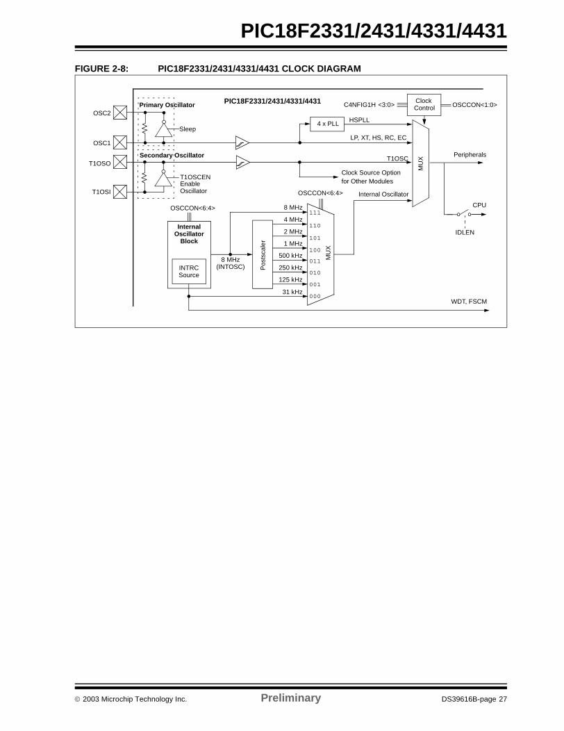
2.7 Clock Sources and Oscillator Switching
Like previous PIC18 devices, the PIC18F2331/2431/4331/4431 devices include a feature that allows thesystem clock source to be switched from the mainoscillator to an alternate low frequency clock source.PIC18F2331/2431/4331/4431 devices offer two alter-nate clock sources. When enabled, these give addi-tional options for switching to the various power-managed operating modes.
Essentially, there are three clock sources for thesedevices:
• Primary oscillators• Secondary oscillators
• Internal oscillator block
The primary oscillators include the external crystaland resonator modes, the external RC modes, theexternal clock modes and the internal oscillator block.The particular mode is defined on POR by the contentsof Configuration Register 1H. The details of thesemodes are covered earlier in this chapter.
The secondary oscillators are those external sourcesnot connected to the OSC1 or OSC2 pins. Thesesources may continue to operate even after thecontroller is placed in a power-managed mode.
PIC18F2331/2431/4331/4431 devices offer only theTimer1 oscillator as a secondary oscillator. Thisoscillator, in all power-managed modes, is often thetime base for functions such as a real-time clock.
Most often, a 32.768 kHz watch crystal is connectedbetween the RC0/T1OSO and RC1/T1OSI pins. Likethe LP mode oscillator circuit, loading capacitors arealso connected from each pin to ground.
The Timer1 oscillator is discussed in greater detail inSection 12.2 “Timer1 Oscillator”.
In addition to being a primary clock source, the internaloscillator block is available as a power-managedmode clock source. The INTRC source is also used asthe clock source for several special features, such asthe WDT and Fail-Safe Clock Monitor.
The clock sources for the PIC18F2331/2431/4331/4431 devices are shown in Figure 2-8. SeeSection 12.0 “Timer1 Module” for further details ofthe Timer1 oscillator. See Section 22.1 “Configura-tion Bits” for Configuration register details.
2.7.1 OSCILLATOR CONTROL REGISTER
The OSCCON register (Register 2-2) controls severalaspects of the system clock’s operation, both in fullpower operation and in power-managed modes.
The System Clock Select bits, SCS1:SCS0, select theclock source that is used when the device is operatingin power-managed modes. The available clock sourcesare the primary clock (defined in Configuration register1H), the secondary clock (Timer1 oscillator) and theinternal oscillator block. The clock selection has noeffect until a SLEEP instruction is executed and thedevice enters a power-managed mode of operation.The SCS bits are cleared on all forms of Reset.
The Internal Oscillator Select bits, IRCF2:IRCF0, selectthe frequency output of the internal oscillator block thatis used to drive the system clock. The choices are theINTRC source, the INTOSC source (8 MHz) or one ofthe six frequencies derived from the INTOSCpostscaler (125 kHz to 4 MHz). If the internal oscillatorblock is supplying the system clock, changing thestates of these bits will have an immediate change onthe internal oscillator’s output.
The OSTS, IOFS and T1RUN bits indicate which clocksource is currently providing the system clock. TheOSTS indicates that the Oscillator Start-up Timer hastimed out, and the primary clock is providing the systemclock in primary clock modes. The IOFS bit indicateswhen the internal oscillator block has stabilized, and isproviding the system clock in RC clock modes. TheT1RUN bit (T1CON<6>) indicates when the Timer1oscillator is providing the system clock in secondaryclock modes. In power-managed modes, only one ofthese three bits will be set at any time. If none of thesebits are set, the INTRC is providing the system clock, orthe internal oscillator block has just started and is notyet stable.
The IDLEN bit controls the selective shut down of thecontroller’s CPU in power-managed modes. The use ofthese bits is discussed in more detail in Section 3.0“Power-Managed Modes”
Note 1: The Timer1 oscillator must be enabled toselect the secondary clock source. TheTimer1 oscillator is enabled by setting theT1OSCEN bit in the Timer1 Control regis-ter (T1CON<3>). If the Timer1 oscillatoris not enabled, then any attempt to selecta secondary clock source when execut-ing a SLEEP instruction will be ignored.
2: It is recommended that the Timer1 oscil-lator be operating and stable before exe-cuting the SLEEP instruction, or a verylong delay may occur while the Timer1oscillator starts.
DS39616B-page 26 Preliminary 2003 Microchip Technology Inc.
PIC18F2331/2431/4331/4431
FIGURE 2-8: PIC18F2331/2431/4331/4431 CLOCK DIAGRAM
PIC18F2331/2431/4331/4431
4 x PLL
C4NFIG1H <3:0>
Secondary Oscillator
T1OSCENEnableOscillator
T1OSO
T1OSI
Clock Source Option for Other Modules
OSC1
OSC2
Sleep
Primary Oscillator
HSPLL
LP, XT, HS, RC, EC
T1OSC
CPU
Peripherals
IDLEN
Pos
tsca
ler
MU
X
MU
X
8 MHz
4 MHz
2 MHz
1 MHz
500 kHz
125 kHz
250 kHz
OSCCON<6:4>
111
110
101
100
011
010
001
00031 kHz
INTRCSource
InternalOscillator
Block
WDT, FSCM
8 MHz
Internal Oscillator
(INTOSC)
OSCCON<6:4>
ClockControl OSCCON<1:0>
2003 Microchip Technology Inc. Preliminary DS39616B-page 27

PIC18F2331/2431/4331/4431
REGISTER 2-2: OSCCON REGISTER
2.7.2 OSCILLATOR TRANSITIONS
The PIC18F2331/2431/4331/4431 devices containcircuitry to prevent clocking “glitches” when switchingbetween clock sources. A short pause in the systemclock occurs during the clock switch. The length of thispause is between 8 and 9 clock periods of the newclock source. This ensures that the new clock source isstable and that its pulse width will not be less than theshortest pulse width of the two clock sources.
Clock transitions are discussed in greater detail inSection 3.1.2 “Entering Power-Managed Modes”.
R/W-0 R/W-0 R/W-0 R/W-0 R(1) R-0 R/W-0 R/W-0IDLEN IRCF2 IRCF1 IRCF0 OSTS IOFS SCS1 SCS0
bit 7 bit 0
bit 7 IDLEN: Idle Enable bit1 = Idle mode enabled; CPU core is not clocked in power-managed modes0 = Run mode enabled; CPU core is clocked in power-managed modes
bit 6-4 IRCF2:IRCF0: Internal Oscillator Frequency Select bits
111 = 8 MHz (8 MHz source drives clock directly)110 = 4 MHz 101 = 2 MHz 100 = 1 MHz 011 = 500 kHz 010 = 250 kHz001 = 125 kHz000 = 31 kHz (INTRC source drives clock directly)
bit 3 OSTS: Oscillator Start-up Time-out Status bit1 = Oscillator start-up time-out timer has expired; primary oscillator is running0 = Oscillator start-up time-out timer is running; primary oscillator is not ready
bit 2 IOFS: INTOSC Frequency Stable bit 1 = INTOSC frequency is stable0 = INTOSC frequency is not stable
bit 1-0 SCS1:SCS0: System Clock Select bits
1x = Internal oscillator block (RC modes)01 = Timer1 oscillator (Secondary modes)00 = Primary oscillator (Sleep and PRI_IDLE modes)
Note 1: Depends on state of the IESO bit in Configuration Register 1H.
Legend:R = Readable bit W = Writable bit U = Unimplemented bit, read as ‘0’- n = Value at POR ‘1’ = Bit is set ‘0’ = Bit is cleared x = Bit is unknown
DS39616B-page 28 Preliminary 2003 Microchip Technology Inc.

PIC18F2331/2431/4331/4431
2.8 Effects of Power-Managed Modes on the Various Clock Sources
When the device executes a SLEEP instruction, thesystem is switched to one of the power-managedmodes, depending on the state of the IDLEN andSCS1:SCS0 bits of the OSCCON register. SeeSection 3.0 “Power-Managed Modes” for details.
When PRI_IDLE mode is selected, the designatedprimary oscillator continues to run without interruption.For all other power-managed modes, the oscillatorusing the OSC1 pin is disabled. The OSC1 pin (andOSC2 pin, if used by the oscillator) will stop oscillating.
In secondary clock modes (SEC_RUN andSEC_IDLE), the Timer1 oscillator is operating andproviding the system clock. The Timer1 oscillator mayalso run in all power-managed modes if required toclock Timer1.
In internal oscillator modes (RC_RUN and RC_IDLE),the internal oscillator block provides the system clocksource. The INTRC output can be used directly toprovide the system clock, and may be enabled tosupport various special features, regardless of thepower-managed mode (see Sections 22.2 through22.4). The INTOSC output at 8 MHz may be used
directly to clock the system, or may be divided downfirst. The INTOSC output is disabled if the system clockis provided directly from the INTRC output.
If the Sleep mode is selected, all clock sources arestopped. Since all the transistor switching currentshave been stopped, Sleep mode achieves the lowestcurrent consumption of the device (only leakagecurrents).
Enabling any on-chip feature that will operate duringSleep will increase the current consumed during Sleep.The INTRC is required to support WDT operation. TheTimer1 oscillator may be operating to support a real-time clock. Other features may be operating that do notrequire a system clock source (i.e., SSP slave, PSP,INTn pins, A/D conversions and others).
2.9 Power-up Delays
Power-up delays are controlled by two timers, so thatno external Reset circuitry is required for mostapplications. The delays ensure that the device is keptin Reset until the device power supply is stable undernormal circumstances, and the primary clock isoperating and stable. For additional information onpower-up delays, see Sections 4.1 through 4.5.
The first timer is the Power-up Timer (PWRT), whichprovides a fixed delay on power-up (parameter 33,Table 25-8), if enabled, in Configuration register 2L.The second timer is the Oscillator Start-up Timer(OST), intended to keep the chip in Reset until the crys-tal oscillator is stable (LP, XT and HS modes). The OSTdoes this by counting 1024 oscillator cycles beforeallowing the oscillator to clock the device.
When the HSPLL Oscillator mode is selected, thedevice is kept in Reset for an additional 2 ms, followingthe HS mode OST delay, so the PLL can lock to theincoming clock frequency.
There is a delay of 5 to 10 µs following POR, while thecontroller becomes ready to execute instructions. Thisdelay runs concurrently with any other delays. Thismay be the only delay that occurs when any of the EC,RC or INTIO modes are used as the primary clocksource.
TABLE 2-3: OSC1 AND OSC2 PIN STATES IN SLEEP MODE
OSC Mode OSC1 Pin OSC2 Pin
RC, INTIO1 Floating, external resistor should pull high
At logic low (clock/4 output)
RCIO, INTIO2 Floating, external resistor should pull high
Configured as PORTA, bit 6
ECIO Floating, pulled by external clock Configured as PORTA, bit 6
EC Floating, pulled by external clock At logic low (clock/4 output)
LP, XT, and HS Feedback inverter disabled, at quiescent voltage level
Feedback inverter disabled, at quiescent voltage level
Note: See Table 4-1 in the Section 4.0 “Reset”, for time-outs due to Sleep and MCLR Reset.
2003 Microchip Technology Inc. Preliminary DS39616B-page 29

PIC18F2331/2431/4331/4431
NOTES:
DS39616B-page 30 Preliminary 2003 Microchip Technology Inc.

PIC18F2331/2431/4331/4431
3.0 POWER-MANAGED MODES
The PIC18F2331/2431/4331/4431 devices offer a totalof six operating modes for more efficient powermanagement (see Table 3-1). These operating modesprovide a variety of options for selective powerconservation in applications where resources may belimited (i.e., battery-powered devices).
There are three categories of power-managed modes:
• Sleep mode • Idle modes
• Run modes
These categories define which portions of the deviceare clocked and sometimes, what speed. The run andidle modes may use any of the three available clocksources (Primary, Secondary or INTOSC multiplexer);the Sleep mode does not use a clock source.
The clock switching feature offered in other PIC18devices (i.e., using the Timer1 oscillator in place of theprimary oscillator), and the Sleep mode offered by allPICmicro® devices (where all system clocks arestopped) are both offered in the PIC18F2331/2431/4331/4431 devices (SEC_RUN and Sleep modes,respectively). However, additional power-managedmodes are available that allow the user greater flexibil-ity in determining what portions of the device are oper-ating. The power-managed modes are event driven;that is, some specific event must occur for the device toenter or (more particularly) exit these operating modes.
For PIC18F2331/2431/4331/4431 devices, the power-managed modes are invoked by using the existingSLEEP instruction. All modes exit to PRI_RUN modewhen triggered by an interrupt, a Reset or a WDT time-out (PRI_RUN mode is the normal full power executionmode; the CPU and peripherals are clocked by the pri-mary oscillator source). In addition, power-managedrun modes may also exit to Sleep mode or theircorresponding idle mode.
3.1 Selecting Power-Managed Modes
Selecting a power-managed mode requires deciding ifthe CPU is to be clocked or not, and selecting a clocksource. The IDLEN bit controls CPU clocking, while theSC1:SCS0 bits select a clock source. The individualmodes, bit settings, clock sources and affectedmodules are summarized in Table 3-1.
3.1.1 CLOCK SOURCES
The clock source is selected by setting the SCS bits ofthe OSCCON register. Three clock sources are avail-able for use in power-managed idle modes: the primaryclock (as configured in Configuration Register 1H), thesecondary clock (Timer1 oscillator), and the internaloscillator block. The secondary and internal oscillatorblock sources are available for the power-managedmodes (PRI_RUN mode is the normal full power exe-cution mode; the CPU and peripherals are clocked bythe primary oscillator source).
TABLE 3-1: POWER-MANAGED MODES
Mode
OSCCON bits Module Clocking
Available Clock and Oscillator SourceIDLEN<7>
SCS1:SCS0<1:0>
CPU Peripherals
Sleep 0 00 Off Off None – All clocks are disabled
PRI_RUN 0 00 Clocked Clocked Primary – LP, XT, HS, HSPLL, RC, EC, INTRC(1)
This is the normal full power execution mode.
SEC_RUN 0 01 Clocked Clocked Secondary – Timer1 Oscillator
RC_RUN 0 1x Clocked Clocked Internal Oscillator Block(1)
PRI_IDLE 1 00 Off Clocked Primary – LP, XT, HS, HSPLL, RC, EC
SEC_IDLE 1 01 Off Clocked Secondary – Timer1 Oscillator
RC_IDLE 1 1x Off Clocked Internal Oscillator Block(1)
Note 1: Includes INTOSC and INTOSC postscaler, as well as the INTRC source.
2003 Microchip Technology Inc. Preliminary DS39616B-page 31

PIC18F2331/2431/4331/4431
3.1.2 ENTERING POWER-MANAGED MODES
In general, entry, exit and switching between power-managed clock sources requires clock source switch-ing. In each case, the sequence of events is the same.
Any change in the power-managed mode begins withloading the OSCCON register and executing a SLEEPinstruction. The SCS1:SCS0 bits select one of threepower-managed clock sources; the primary clock (asdefined in Configuration Register 1H), the secondaryclock (the Timer1 oscillator) and the internal oscillatorblock (used in RC modes). Modifying the SCS bits willhave no effect until a SLEEP instruction is executed.Entry to the power-managed mode is triggered by theexecution of a SLEEP instruction.
Figure 3-5 shows how the system is clocked whileswitching from the primary clock to the Timer1 oscilla-tor. When the SLEEP instruction is executed, clocks tothe device are stopped at the beginning of the nextinstruction cycle. Eight clock cycles from the new clocksource are counted to synchronize with the new clocksource. After eight clock pulses from the new clocksource are counted, clocks from the new clock sourceresume clocking the system. The actual length of thepause is between eight and nine clock periods from thenew clock source. This ensures that the new clocksource is stable and that its pulse width will not be lessthan the shortest pulse width of the two clock sources.
Three bits indicate the current clock source: OSTS andIOFS in the OSCCON register, and T1RUN in theT1CON register. Only one of these bits will be set whilein a power-managed mode other than PRI_RUN. Whenthe OSTS bit is set, the primary clock is providing thesystem clock. When the IOFS bit is set, the INTOSCoutput is providing a stable 8 MHz clock source and isproviding the system clock. When the T1RUN bit is set,the Timer1 oscillator is providing the system clock. Ifnone of these bits are set, then either the INTRC clocksource is clocking the system, or the INTOSC source isnot yet stable.
If the internal oscillator block is configured as the pri-mary clock source in Configuration Register 1H, thenboth the OSTS and IOFS bits may be set when inPRI_RUN or PRI_IDLE modes. This indicates that theprimary clock (INTOSC output) is generating a stable8 MHz output. Entering an RC power-managed mode(same frequency) would clear the OSTS bit.
3.1.3 MULTIPLE SLEEP COMMANDS
The power-managed mode that is invoked with theSLEEP instruction is determined by the settings of theIDLEN and SCS bits at the time the instruction is exe-cuted. If another SLEEP instruction is executed, thedevice will enter the power-managed mode specifiedby these same bits at that time. If the bits havechanged, the device will enter the new power-managedmode specified by the new bit settings.
3.1.4 COMPARISONS BETWEEN RUN AND IDLE MODES
Clock source selection for the run modes is identical tothe corresponding idle modes. When a SLEEP instruc-tion is executed, the SCS bits in the OSCCON registerare used to switch to a different clock source. As aresult, if there is a change of clock source at the time aSLEEP instruction is executed, a clock switch will occur.
In idle modes, the CPU is not clocked and is not run-ning. In run modes, the CPU is clocked and executingcode. This difference modifies the operation of theWDT when it times out. In idle modes, a WDT time-outresults in a wake from power-managed modes. In runmodes, a WDT time-out results in a WDT Reset (seeTable 3-2).
During a wake-up from an idle mode, the CPU startsexecuting code by entering the corresponding runmode, until the primary clock becomes ready. When theprimary clock becomes ready, the clock source is auto-matically switched to the primary clock. The IDLEN andSCS bits are unchanged during and after the wake-up.
Figure 3-2 shows how the system is clocked during theclock source switch. The example assumes the devicewas in SEC_IDLE or SEC_RUN mode when a wake istriggered (the primary clock was configured in HSPLLmode).
Note 1: Caution should be used when modifying asingle IRCF bit. If VDD is less than 3V, it ispossible to select a higher clock speedthan is supported by the low VDD.Improper device operation may result ifthe VDD/FOSC specifications are violated.
2: Executing a SLEEP instruction does notnecessarily place the device into Sleepmode; executing a SLEEP instruction issimply a trigger to place the controller intoa power-managed mode selected by theOSCCON register, one of which is Sleepmode.
DS39616B-page 32 Preliminary 2003 Microchip Technology Inc.

PIC18F2331/2431/4331/4431
3.2 Sleep Mode
The power-managed Sleep mode in the PIC18F2331/2431/4331/4431 devices is identical to that offered inall other PICmicro® controllers. It is entered by clearingthe IDLEN and SCS1:SCS0 bits (this is the Resetstate), and executing the SLEEP instruction. This shutsdown the primary oscillator and the OSTS bit is cleared(see Figure 3-1).
When a wake event occurs in Sleep mode (by interrupt,Reset, or WDT time-out), the system will not be clockeduntil the primary clock source becomes ready (seeFigure 3-2), or it will be clocked from the internal oscil-lator block if either the Two-Speed Start-up or the Fail-Safe Clock Monitor are enabled (see Section 22.0“Special Features of the CPU”). In either case, theOSTS bit is set when the primary clock provides thesystem clocks. The IDLEN and SCS bits are notaffected by the wake-up.
3.3 Idle Modes
The IDLEN bit allows the controller’s CPU to be selec-tively shut down while the peripherals continue to oper-ate. Clearing IDLEN allows the CPU to be clocked.Setting IDLEN disables clocks to the CPU, effectivelystopping program execution (see Register 2-2). Theperipherals continue to be clocked regardless of thesetting of the IDLEN bit.
There is one exception to how the IDLEN bit functions.When all the low-power OSCCON bits are cleared(IDLEN:SCS1:SCS0 = 000), the device enters Sleepmode upon the execution of the SLEEP instruction. Thisis both the Reset state of the OSCCON register and thesetting that selects Sleep mode. This maintains com-patibility with other PICmicro devices that do not offerpower-managed modes.
If the Idle Enable bit, IDLEN (OSCCON<7>), is set to a‘1’ when a SLEEP instruction is executed, theperipherals will be clocked from the clock sourceselected using the SCS1:SCS0 bits; however, the CPUwill not be clocked. Since the CPU is not executinginstructions, the only exits from any of the idle modesare by interrupt, WDT time-out or a Reset.
When a wake event occurs, CPU execution is delayedapproximately 10 µs while it becomes ready to executecode. When the CPU begins executing code, it isclocked by the same clock source as was selected inthe power-managed mode (i.e., when waking fromRC_IDLE mode, the internal oscillator block will clockthe CPU and peripherals until the primary clock sourcebecomes ready – this is essentially RC_RUN mode).This continues until the primary clock source becomesready. When the primary clock becomes ready, theOSTS bit is set, and the system clock source isswitched to the primary clock (see Figure 3-4). TheIDLEN and SCS bits are not affected by the wake-up.
While in any idle mode or the Sleep mode, a WDT time-out will result in a WDT wake-up to full power operation.
TABLE 3-2: COMPARISON BETWEEN POWER-MANAGED MODES
Power Managed
ModeCPU is clocked by ...
WDT time-out causes a ...
Peripherals are clocked by ...
Clock during wake-up (while primary becomes
ready)
Sleep Not clocked (not running) Wake-up Not clocked None or INTOSC multiplexer if Two-Speed Start-up or Fail-Safe Clock Monitor are enabled.
Any idle mode Not clocked (not running) Wake-up Primary, Secondary or INTOSC multiplexer
Unchanged from Idle mode (CPU operates as in corresponding Run mode).
Any run mode Secondary, or INTOSC multiplexer
Reset Secondary or INTOSC multiplexer
Unchanged from Run mode.
2003 Microchip Technology Inc. Preliminary DS39616B-page 33

PIC18F2331/2431/4331/4431
FIGURE 3-1: TIMING TRANSITION FOR ENTRY TO SLEEP MODE
FIGURE 3-2: TRANSITION TIMING FOR WAKE FROM SLEEP (HSPLL)
Q4Q3Q2
OSC1
Peripheral
Sleep
Program
Q1Q1
Counter
Clock
CPUClock
PC + 2PC
Q3 Q4 Q1 Q2
OSC1
Peripheral
Program PC
PLL Clock
Q3 Q4
Output
CPU Clock
Q1 Q2 Q3 Q4 Q1 Q2
Clock
Counter PC + 8PC + 6
Q1 Q2 Q3 Q4
Wake Event
Note 1: TOST = 1024 TOSC; TPLL = 2 ms (approx). These intervals are not shown to scale.
TOST(1)TPLL(1)
OSTS bit Set
PC + 4PC + 2
DS39616B-page 34 Preliminary 2003 Microchip Technology Inc.

PIC18F2331/2431/4331/4431
3.3.1 PRI_IDLE MODE
This mode is unique among the three low-power idlemodes, in that it does not disable the primary systemclock. For timing sensitive applications, this allows forthe fastest resumption of device operation with its moreaccurate primary clock source, since the clock sourcedoes not have to “warm up” or transition from anotheroscillator.
PRI_IDLE mode is entered by setting the IDLEN bit,clearing the SCS bits, and executing a SLEEP instruc-tion. Although the CPU is disabled, the peripheralscontinue to be clocked from the primary clock sourcespecified in Configuration Register 1H. The OSTS bitremains set in PRI_IDLE mode (see Figure 3-3).
When a wake event occurs, the CPU is clocked from theprimary clock source. A delay of approximately 10 µs isrequired between the wake event and when code exe-cution starts. This is required to allow the CPU tobecome ready to execute instructions. After the wake-up, the OSTS bit remains set. The IDLEN and SCS bitsare not affected by the wake-up (see Figure 3-4).
FIGURE 3-3: TRANSITION TIMING TO PRI_IDLE MODE
FIGURE 3-4: TRANSITION TIMING FOR WAKE FROM PRI_IDLE MODE
Q1
Peripheral
Program PC PC + 2
OSC1
Q3 Q4 Q1
CPU Clock
Clock
Counter
Q2
OSC1
Peripheral
Program PC
CPU Clock
PC + 2
Q1 Q3 Q4
Clock
Counter
Q2
Wake Event
CPU Start-up Delay
2003 Microchip Technology Inc. Preliminary DS39616B-page 35

PIC18F2331/2431/4331/4431
3.3.2 SEC_IDLE MODE
In SEC_IDLE mode, the CPU is disabled, but theperipherals continue to be clocked from the Timer1oscillator. This mode is entered by setting the Idle bit,modifying to SCS1:SCS0 = 01, and executing a SLEEPinstruction. When the clock source is switched (seeFigure 3-5) to the Timer1 oscillator, the primary oscilla-tor is shut down, the OSTS bit is cleared and theT1RUN bit is set.
When a wake event occurs, the peripherals continue tobe clocked from the Timer1 oscillator. After a 10 µsdelay following the wake event, the CPU begins execut-ing code, being clocked by the Timer1 oscillator. Themicrocontroller operates in SEC_RUN mode until theprimary clock becomes ready. When the primary clockbecomes ready, a clock switch back to the primary clockoccurs (see Figure 3-6). When the clock switch is com-plete, the T1RUN bit is cleared, the OSTS bit is set andthe primary clock is providing the system clock. TheIDLEN and SCS bits are not affected by the wake-up;the Timer1 oscillator continues to run.
FIGURE 3-5: TIMING TRANSITION FOR ENTRY TO SEC_IDLE MODE
FIGURE 3-6: TIMING TRANSITION FOR WAKE FROM SEC_RUN MODE (HSPLL)
Note: The Timer1 oscillator should already berunning prior to entering SEC_IDLE mode.If the T1OSCEN bit is not set when theSLEEP instruction is executed, a forcedNOP will be executed instead and entry toSEC_IDLE mode will not occur. If theTimer1 oscillator is enabled, but not yetrunning, peripheral clocks will be delayeduntil the oscillator has started; in such sit-uations, initial oscillator operation is farfrom stable and unpredictable operationmay result.
Q4Q3Q2
OSC1
Peripheral
Program
Q1
T1OSI
Q1
Counter
Clock
CPUClock
PC + 2PC
1 2 3 4 5 6 7 8
Clock Transition
Q1 Q3 Q4
OSC1
Peripheral
Program PC PC + 2
T1OSI
PLL Clock
Q1
PC + 6
Q2
Output
Q3 Q4 Q1
CPU Clock
PC + 4
Clock
Counter
Q2 Q2 Q3
Note 1: TOST = 1024 TOSC; TPLL = 2 ms (approx). These intervals are not shown to scale.
Wake from Interrupt Event
TOST(1)TPLL(1)
1 2 3 4 5 6 7 8Clock Transition
OSTS bit Set
DS39616B-page 36 Preliminary 2003 Microchip Technology Inc.

PIC18F2331/2431/4331/4431
3.3.3 RC_IDLE MODE
In RC_IDLE mode, the CPU is disabled, but the periph-erals continue to be clocked from the internal oscillatorblock using the INTOSC multiplexer. This mode allowsfor controllable power conservation during Idle periods.
This mode is entered by setting the IDLEN bit, settingSCS1 (SCS0 is ignored), and executing a SLEEPinstruction. The INTOSC multiplexer may be used toselect a higher clock frequency by modifying the IRCFbits before executing the SLEEP instruction. When theclock source is switched to the INTOSC multiplexer(see Figure 3-7), the primary oscillator is shut down,and the OSTS bit is cleared.
If the IRCF bits are set to a non-zero value (thusenabling the INTOSC output), the IOFS bit becomesset after the INTOSC output becomes stable, in about1 ms. Clocks to the peripherals continue while theINTOSC source stabilizes. If the IRCF bits were previ-ously at a non-zero value before the SLEEP instruction
was executed, and the INTOSC source was alreadystable, the IOFS bit will remain set. If the IRCF bits areall clear, the INTOSC output is not enabled and theIOFS bit will remain clear; there will be no indication ofthe current clock source.
When a wake event occurs, the peripherals continue tobe clocked from the INTOSC multiplexer. After a 10 µsdelay following the wake event, the CPU begins exe-cuting code, being clocked by the INTOSC multiplexer.The microcontroller operates in RC_RUN mode untilthe primary clock becomes ready. When the primaryclock becomes ready, a clock switch back to the pri-mary clock occurs (see Figure 3-8). When the clockswitch is complete, the IOFS bit is cleared, the OSTSbit is set, and the primary clock is providing the systemclock. The IDLEN and SCS bits are not affected by thewake-up. The INTRC source will continue to run ifeither the WDT or the Fail-Safe Clock Monitor isenabled.
FIGURE 3-7: TIMING TRANSITION TO RC_IDLE MODE
FIGURE 3-8: TIMING TRANSITION FOR WAKE FROM RC_RUN MODE (RC_RUN TO PRI_RUN)
Q4Q3Q2
OSC1
Peripheral
Program
Q1
INTRC
Q1
Counter
Clock
CPUClock
PC + 2PC
1 2 3 4 5 6 7 8
Clock Transition
Q1 Q3 Q4
OSC1
Peripheral
Program PC PC + 2
INTOSC
PLL Clock
Q1
PC + 6
Q2
Output
Q3 Q4 Q1
CPU Clock
PC + 4
Clock
Counter
Q2 Q2 Q3
Note 1: TOST = 1024 TOSC; TPLL = 2 ms (approx). These intervals are not shown to scale.
Wake from Interrupt Event
TOST(1)TPLL(1)
1 2 3 4 5 6 7 8Clock Transition
OSTS bit Set
Multiplexer
Q4
2003 Microchip Technology Inc. Preliminary DS39616B-page 37

PIC18F2331/2431/4331/4431
3.4 Run Modes
If the IDLEN bit is clear when a SLEEP instruction isexecuted, the CPU and peripherals are both clockedfrom the source selected using the SCS1:SCS0 bits.While these operating modes may not afford the powerconservation of Idle or Sleep modes, they do allow thedevice to continue executing instructions by using alower frequency clock source. RC_RUN mode alsooffers the possibility of executing code at a frequencygreater than the primary clock.
Wake-up from a power-managed run mode can be trig-gered by an interrupt, or any Reset, to return to fullpower operation. As the CPU is executing code in runmodes, several additional exits from run modes arepossible. They include exit to Sleep mode, exit to a cor-responding idle mode, and exit by executing a RESETinstruction. While the device is in any of the power-managed run modes, a WDT time-out will result in aWDT Reset.
3.4.1 PRI_RUN MODE
The PRI_RUN mode is the normal full power executionmode. If the SLEEP instruction is never executed, themicrocontroller operates in this mode (a SLEEP instruc-tion is executed to enter all other power-managedmodes). All other power-managed modes exit toPRI_RUN mode when an interrupt or WDT time-outoccur.
There is no entry to PRI_RUN mode. The OSTS bit isset. The IOFS bit may be set if the internal oscillatorblock is the primary clock source (see Section 2.7.1“Oscillator Control Register”).
3.4.2 SEC_RUN MODE
The SEC_RUN mode is the compatible mode to the“clock switching” feature offered in other PIC18devices. In this mode, the CPU and peripherals areclocked from the Timer1 oscillator. This gives users theoption of lower power consumption while still using ahigh accuracy clock source.
SEC_RUN mode is entered by clearing the IDLEN bit,setting SCS1:SCS0 = 01, and executing a SLEEPinstruction. The system clock source is switched to theTimer1 oscillator (see Figure 3-9), the primary oscilla-tor is shut down, the T1RUN bit (T1CON<6>) is set andthe OSTS bit is cleared.
When a wake event occurs, the peripherals and CPUcontinue to be clocked from the Timer1 oscillator whilethe primary clock is started. When the primary clockbecomes ready, a clock switch back to the primary clockoccurs (see Figure 3-6). When the clock switch is com-plete, the T1RUN bit is cleared, the OSTS bit is set, andthe primary clock is providing the system clock. TheIDLEN and SCS bits are not affected by the wake-up;the Timer1 oscillator continues to run.
Firmware can force an exit from SEC_RUN mode. Byclearing the T1OSCEN bit (T1CON<3>), an exit fromSEC_RUN back to normal full power operation is trig-gered. The Timer1 oscillator will continue to run andprovide the system clock even though the T1OSCEN bitis cleared. The primary clock is started. When the pri-mary clock becomes ready, a clock switch back to theprimary clock occurs (see Figure 3-6). When the clockswitch is complete, the Timer1 oscillator is disabled, theT1RUN bit is cleared, the OSTS bit is set and the pri-mary clock provides the system clock. The IDLEN andSCS bits are not affected by the wake-up.
FIGURE 3-9: TIMING TRANSITION FOR ENTRY TO SEC_RUN MODE
Note: The Timer1 oscillator should already berunning prior to entering SEC_RUN mode.If the T1OSCEN bit is not set when theSLEEP instruction is executed, a forcedNOP will be executed instead and entry toSEC_IDLE mode will not occur. If theTimer1 oscillator is enabled, but not yetrunning, system clocks will be delayeduntil the oscillator has started. In suchsituations, initial oscillator operation is farfrom stable and unpredictable operationmay result.
Q4Q3Q2
OSC1
Peripheral
Program
Q1
T1OSI
Q1
Counter
Clock
CPUClock
PC + 2PC
1 2 3 4 5 6 7 8
Clock Transition
Q4Q3Q2 Q1 Q3Q2
PC + 2
DS39616B-page 38 Preliminary 2003 Microchip Technology Inc.

PIC18F2331/2431/4331/4431
3.4.3 RC_RUN MODE
In RC_RUN mode, the CPU and peripherals areclocked from the internal oscillator block using theINTOSC multiplexer, and the primary clock is shutdown. When using the INTRC source, this mode pro-vides the best power conservation of all the run modes,while still executing code. This mode works well foruser applications that are not highly timing sensitive, ordo not require high-speed clocks at all times.
If the primary clock source is the internal oscillatorblock (either of the INTIO1 or INTIO2 oscillators), thereare no distinguishable differences between PRI_RUNand RC_RUN modes during execution. However, aclock switch delay will occur during entry to, and exitfrom, RC_RUN mode. Therefore, if the primary clocksource is the internal oscillator block, the use ofRC_RUN mode is not recommended.
This mode is entered by clearing the IDLEN bit, settingSCS1 (SCS0 is ignored) and executing a SLEEPinstruction. The IRCF bits may select the clockfrequency before the SLEEP instruction is executed.When the clock source is switched to the INTOSCmultiplexer (see Figure 3-10), the primary oscillator isshut down and the OSTS bit is cleared.
The IRCF bits may be modified at any time to immedi-ately change the system clock speed. Executing aSLEEP instruction is not required to select a new clockfrequency from the INTOSC multiplexer.
If the IRCF bits are all clear, the INTOSC output is notenabled, and the IOFS bit will remain clear; there willbe no indication of the current clock source. The INTRCsource is providing the system clocks.
If the IRCF bits are changed from all clear (thusenabling the INTOSC output), the IOFS bit becomesset after the INTOSC output becomes stable. Clocks tothe system continue while the INTOSC sourcestabilizes in approximately 1 ms.
If the IRCF bits were previously at a non-zero valuebefore the SLEEP instruction was executed, and theINTOSC source was already stable, the IOFS bit willremain set.
When a wake event occurs, the system continues to beclocked from the INTOSC multiplexer while the primaryclock is started. When the primary clock becomesready, a clock switch to the primary clock occurs (seeFigure 3-8). When the clock switch is complete, theIOFS bit is cleared, the OSTS bit is set and the primaryclock provides the system clock. The IDLEN and SCSbits are not affected by the wake-up. The INTRCsource will continue to run if either the WDT or theFail-Safe Clock Monitor is enabled.
FIGURE 3-10: TIMING TRANSITION TO RC_RUN MODE
Note: Caution should be used when modifying asingle IRCF bit. If VDD is less than 3V, it ispossible to select a higher clock speedthan is supported by the low VDD.Improper device operation may result ifthe VDD/FOSC specifications are violated.
Q3Q2Q1
OSC1
Peripheral
Program
Q4
INTRC
Q4
Counter
Clock
CPUClock
PC + 2PC
1 2 3 4 5 6 7 8
Clock Transition
Q3Q2Q1 Q4 Q2Q1 Q3
PC + 4
2003 Microchip Technology Inc. Preliminary DS39616B-page 39

PIC18F2331/2431/4331/4431
3.4.4 EXIT TO IDLE MODE
An exit from a power-managed run mode to its corre-sponding idle mode is executed by setting the IDLENbit and executing a SLEEP instruction. The CPU ishalted at the beginning of the instruction following theSLEEP instruction. There are no changes to any of theclock source status bits (OSTS, IOFS, or T1RUN).While the CPU is halted, the peripherals continue to beclocked from the previously selected clock source.
3.4.5 EXIT TO SLEEP MODE
An exit from a power-managed run mode to Sleepmode is executed by clearing the IDLEN andSCS1:SCS0 bits and executing a SLEEP instruction.The code is no different than the method used to invokeSleep mode from the normal operating (full power)mode.
The primary clock and internal oscillator block are dis-abled. The INTRC will continue to operate if the WDTis enabled. The Timer1 oscillator will continue to run, ifenabled, in the T1CON register. All clock source statusbits are cleared (OSTS, IOFS and T1RUN).
3.5 Wake From Power-Managed Modes
An exit from any of the power-managed modes is trig-gered by an interrupt, a Reset or a WDT time-out. Thissection discusses the triggers that cause exits frompower-managed modes. The clocking subsystemactions are discussed in each of the power-managedmodes (see Sections 3.2 through 3.4).
Device behavior during Low-power mode exits issummarized in Table 3-3.
3.5.1 EXIT BY INTERRUPT
Any of the available interrupt sources can cause thedevice to exit a power-managed mode and resume fullpower operation. To enable this functionality, an inter-rupt source must be enabled by setting its enable bit inone of the INTCON or PIE registers. The exit sequenceis initiated when the corresponding interrupt flag bit isset. On all exits from Low-power mode by interrupt,code execution branches to the interrupt vector if theGIE/GIEH bit (INTCON<7>) is set. Otherwise, codeexecution continues or resumes without branching(see Section 9.0 “Interrupts”).
Note: If application code is timing sensitive, itshould wait for the OSTS bit to become setbefore continuing. Use the interval duringthe Low-power exit sequence (beforeOSTS is set) to perform timing insensitive“housekeeping” tasks.
DS39616B-page 40 Preliminary 2003 Microchip Technology Inc.

PIC18F2331/2431/4331/4431
TABLE 3-3: ACTIVITY AND EXIT DELAY ON WAKE FROM SLEEP MODE OR ANY IDLE MODE(BY CLOCK SOURCES)
Clock in Power- Managed Mode
Primary System Clock
Power- Managed Mode Exit
Delay
Clock Ready Status bit (OSCCON)
Activity During Wake from Power-Managed Mode
Exit by Interrupt Exit by Reset
Primary System Clock(PRI_IDLE mode)
LP, XT, HS
5-10 µs(5)OSTS
CPU and peripherals clocked by primary clock and executing instructions.
Not clocked, or Two-Speed Start-up (if enabled)(3).
HSPLL
EC, RC, INTRC(1) —
INTOSC(2) IOFS
T1OSC or INTRC(1)
LP, XT, HS OSTOSTS
CPU and peripherals clocked by selected power-managed mode clock and executing instructions until primary clock source becomes ready.
HSPLL OST + 2 ms
EC, RC, INTRC(1) 5-10 µs(5) —
INTOSC(2) 1 ms(4) IOFS
INTOSC(2)
LP, XT, HS OSTOSTS
HSPLL OST + 2 ms
EC, RC, INTRC(1) 5-10 µs(5) —
INTOSC(2) None IOFS
Sleep mode
LP, XT, HS OSTOSTS
Not clocked or Two-Speed Start-up (if enabled) until primary clock source becomes ready(3).
HSPLL OST + 2 ms
EC, RC, INTRC(1) 5-10 µs(5) —
INTOSC(2) 1 ms(4) IOFS
Note 1: In this instance, refers specifically to the INTRC clock source.
2: Includes both the INTOSC 8 MHz source and postscaler derived frequencies.3: Two-Speed Start-up is covered in greater detail in Section 22.3 “Two-Speed Start-up”.4: Execution continues during the INTOSC stabilization period.
5: Required delay when waking from Sleep and all idle modes. This delay runs concurrently with any other required delays (see Section 3.3 “Idle Modes”).
2003 Microchip Technology Inc. Preliminary DS39616B-page 41

PIC18F2331/2431/4331/4431
3.5.2 EXIT BY RESET
Normally, the device is held in Reset by the OscillatorStart-up Timer (OST) until the primary clock (defined inConfiguration register 1H) becomes ready. At that time,the OSTS bit is set and the device begins executingcode.
Code execution can begin before the primary clockbecomes ready. If either the Two-Speed Start-up (seeSection 22.3 “Two-Speed Start-up”) or Fail-SafeClock Monitor (see Section 22.4 “Fail-Safe ClockMonitor”) are enabled in Configuration Register 1H,the device may begin execution as soon as the Resetsource has cleared. Execution is clocked by theINTOSC multiplexer driven by the internal oscillatorblock. Since the OSCCON register is cleared followingall Resets, the INTRC clock source is selected. Ahigher speed clock may be selected by modifying theIRCF bits in the OSCCON register. Execution isclocked by the internal oscillator block until either theprimary clock becomes ready, or a power-managedmode is entered before the primary clock becomesready; the primary clock is then shut down.
3.5.3 EXIT BY WDT TIME-OUT
A WDT time-out will cause different actions dependingon which power-managed mode the device is in whenthe time-out occurs.
If the device is not executing code (all idle modes andSleep mode), the time-out will result in a wake from thepower-managed mode (see Section 3.2 “SleepMode” through Section 3.4 “Run Modes”).
If the device is executing code (all run modes), thetime-out will result in a WDT Reset (see Section 22.2“Watchdog Timer (WDT)”).
The WDT timer and postscaler are cleared by execut-ing a SLEEP or CLRWDT instruction, the loss of a cur-rently selected clock source (if the Fail-Safe ClockMonitor is enabled), and modifying the IRCF bits in theOSCCON register if the internal oscillator block is thesystem clock source.
3.5.4 EXIT WITHOUT AN OSCILLATOR START-UP DELAY
Certain exits from power-managed modes do notinvoke the OST at all. These are:
• PRI_IDLE mode where the primary clock source is not stopped; and
• the primary clock source is not any of LP, XT, HS or HSPLL modes.
In these cases, the primary clock source either doesnot require an oscillator start-up delay, since it isalready running (PRI_IDLE), or normally does notrequire an oscillator start-up delay (RC, EC, and INTIOoscillator modes).
However, a fixed delay (approximately 10 µs) followingthe wake event is required when leaving Sleep and idlemodes. This delay is required for the CPU to preparefor execution. Instruction execution resumes on the firstclock cycle following this delay.
3.6 INTOSC Frequency Drift
The factory calibrates the internal oscillator block out-put (INTOSC) for 8 MHz. However, this frequency maydrift as VDD or temperature changes, which can affectthe controller operation in a variety of ways.
It is possible to adjust the INTOSC frequency by modi-fying the value in the OSCTUNE register. This has theside effect that the INTRC clock source frequency isalso affected. However, the features that use theINTRC source often do not require an exact frequency.These features include the Fail-Safe Clock Monitor, theWatchdog Timer and the RC_RUN/RC_IDLE modeswhen the INTRC clock source is selected.
Being able to adjust the INTOSC requires knowingwhen an adjustment is required, in which direction itshould be made, and in some cases, how large achange is needed. Three examples follow, but othertechniques may be used.
DS39616B-page 42 Preliminary 2003 Microchip Technology Inc.

PIC18F2331/2431/4331/4431
3.6.1 EXAMPLE – USART
An adjustment may be indicated when the USARTbegins to generate framing errors, or receives data witherrors while in Asynchronous mode. Framing errorsindicate that the system clock frequency is too high –try decrementing the value in the OSCTUNE register toreduce the system clock frequency. Errors in datamay suggest that the system clock speed is too low –increment OSCTUNE.
3.6.2 EXAMPLE – TIMERS
This technique compares system clock speed to somereference clock. Two timers may be used; one timer isclocked by the peripheral clock, while the other isclocked by a fixed reference source, such as theTimer1 oscillator.
Both timers are cleared, but the timer clocked by thereference generates interrupts. When an interruptoccurs, the internally clocked timer is read and bothtimers are cleared. If the internally clocked timer valueis greater than expected, then the internal oscillatorblock is running too fast – decrement OSCTUNE.
3.6.3 EXAMPLE – CCP IN CAPTURE MODE
A CCP module can use free running Timer1, clocked bythe internal oscillator block and an external event witha known period (i.e., AC power frequency). The time ofthe first event is captured in the CCPRxH:CCPRxLregisters and is recorded for use later. When thesecond event causes a capture, the time of the firstevent is subtracted from the time of the second event.Since the period of the external event is known, thetime difference between events can be calculated.
If the measured time is much greater than thecalculated time, the internal oscillator block is runningtoo fast – decrement OSCTUNE. If the measured timeis much less than the calculated time, the internaloscillator block is running too slow – incrementOSCTUNE.
2003 Microchip Technology Inc. Preliminary DS39616B-page 43

PIC18F2331/2431/4331/4431
NOTES:
DS39616B-page 44 Preliminary 2003 Microchip Technology Inc.

PIC18F2331/2431/4331/4431
4.0 RESET
The PIC18F2331/2431/4331/4431 devices differenti-ate between various kinds of Reset:
a) Power-on Reset (POR)
b) MCLR Reset during normal operationc) MCLR Reset during Sleep d) Watchdog Timer (WDT) Reset (during
execution)e) Programmable Brown-out Reset (BOR)
f) RESET Instructiong) Stack Full Reseth) Stack Underflow Reset
Most registers are unaffected by a Reset. Their statusis unknown on POR and unchanged by all otherResets. The other registers are forced to a “Resetstate” depending on the type of Reset that occurred.
Most registers are not affected by a WDT wake-up,since this is viewed as the resumption of normaloperation. Status bits from the RCON register, RI, TO,PD, POR and BOR, are set or cleared differently indifferent Reset situations, as indicated in Table 4-2.These bits are used in software to determine the natureof the Reset. See Table 4-3 for a full description of theReset states of all registers.
A simplified block diagram of the On-Chip Reset Circuitis shown in Figure 4-1.
The enhanced MCU devices have a MCLR noise filterin the MCLR Reset path. The filter will detect andignore small pulses.
The MCLR pin is not driven low by any internal Resets,including the WDT.
The MCLR input provided by the MCLR pin can be dis-abled with the MCLRE bit in Configuration Register 3H(CONFIG3H<7>). See Section 22.1 “ConfigurationBits” for more information.
FIGURE 4-1: SIMPLIFIED BLOCK DIAGRAM OF ON-CHIP RESET CIRCUIT
S
R Q
External Reset
MCLR
VDD
OSC1
WDTTime-out
VDD RiseDetect
OST/PWRT
INTRC(1)
POR Pulse
OST
10-bit Ripple Counter
PWRT
Chip_Reset
11-bit Ripple Counter
Enable OST(2)
Enable PWRT
Note 1: This is the INTRC source from the internal oscillator block, and is separate from the RC oscillator of the CLKI pin.
2: See Table 4-1 for time-out situations.
Brown-outReset
BOREN
RESETInstruction
StackPointer
Stack Full/Underflow Reset
Sleep( )_IDLE
1024 Cycles
65.5 ms32 µs
MCLRE
2003 Microchip Technology Inc. Preliminary DS39616B-page 45

PIC18F2331/2431/4331/4431
4.1 Power-on Reset (POR)
A Power-on Reset pulse is generated on-chip whenVDD rise is detected. To take advantage of the POR cir-cuitry, just tie the MCLR pin through a resistor (1k to10 kΩ) to VDD. This will eliminate external RC compo-nents usually needed to create a Power-on Resetdelay. A minimum rise rate for VDD is specified(parameter D004). For a slow rise time, see Figure 4-2.
When the device starts normal operation (i.e., exits theReset condition), device operating parameters (volt-age, frequency, temperature, etc.) must be met toensure operation. If these conditions are not met, thedevice must be held in Reset until the operatingconditions are met.
FIGURE 4-2: EXTERNAL POWER-ON RESET CIRCUIT (FOR SLOW VDD POWER-UP)
4.2 Power-up Timer (PWRT)
The Power-up Timer (PWRT) of the PIC18F2331/2431/4331/4431 devices is an 11-bit counter, which uses theINTRC source as the clock input. This yields a count of2048 x 32 µs = 65.6 ms. While the PWRT is counting,the device is held in Reset.
The power-up time delay depends on the INTRC clockand will vary from chip-to-chip due to temperature andprocess variation. See DC parameter #33 for details.
The PWRT is enabled by clearing configuration bitPWRTEN.
4.3 Oscillator Start-up Timer (OST)
The Oscillator Start-up Timer (OST) provides a 1024oscillator cycle (from OSC1 input) delay after thePWRT delay is over (parameter #33). This ensures thatthe crystal oscillator or resonator has started andstabilized.
The OST time-out is invoked only for XT, LP, HS andHSPLL modes, and only on Power-on Reset or on exitfrom most power-managed modes.
4.4 PLL Lock Time-out
With the PLL enabled in its PLL mode, the time-outsequence following a Power-on Reset is slightly differ-ent from other oscillator modes. A portion of the Power-up Timer is used to provide a fixed time-out that is suf-ficient for the PLL to lock to the main oscillator fre-quency. This PLL lock time-out (TPLL) is typically 2 msand follows the oscillator start-up time-out.
4.5 Brown-out Reset (BOR)
A configuration bit, BOREN, can disable (if clear/programmed) or enable (if set) the Brown-out Reset cir-cuitry. If VDD falls below VBOR (parameter D005) forgreater than TBOR (parameter #35), the brown-out situ-ation will reset the chip. A Reset may not occur if VDD
falls below VBOR for less than TBOR. The chip willremain in Brown-out Reset until VDD rises above VBOR.If the Power-up Timer is enabled, it will be invoked afterVDD rises above VBOR; it then will keep the chip inReset for an additional time delay TPWRT (parameter#33). If VDD drops below VBOR while the Power-upTimer is running, the chip will go back into a Brown-outReset and the Power-up Timer will be initialized. OnceVDD rises above VBOR, the Power-up Timer will executethe additional time delay. Enabling BOR Reset doesnot automatically enable the PWRT.
4.6 Time-out Sequence
On power-up, the time-out sequence is as follows:First, after the POR pulse has cleared, PWRT time-outis invoked (if enabled). Then, the OST is activated. Thetotal time-out will vary based on oscillator configurationand the status of the PWRT. For example, in RC modewith the PWRT disabled, there will be no time-out at all.Figures 4-3 through 4-7 depict time-out sequences onpower-up.
Since the time-outs occur from the POR pulse, if MCLRis kept low long enough, all time-outs will expire. Bring-ing MCLR high will begin execution immediately(Figure 4-5). This is useful for testing purposes or tosynchronize more than one PIC18FXXXX deviceoperating in parallel.
Table 4-2 shows the Reset conditions for some SpecialFunction registers, while Table 4-3 shows the Resetconditions for all the registers.
Note 1: External Power-on Reset circuit isrequired only if the VDD power-up slopeis too slow. The diode D helps dischargethe capacitor quickly when VDD powersdown.
2: R < 40 kΩ is recommended to makesure that the voltage drop across R doesnot violate the device’s electrical specifi-cation.
3: R1 ≥ 1 kΩ will limit any current flowinginto MCLR from external capacitor C, inthe event of MCLR/VPP pin breakdown,due to Electrostatic Discharge (ESD) orElectrical Overstress (EOS).
C
R1RD
VDD
MCLR
PIC18FXXXX
VDD
DS39616B-page 46 Preliminary 2003 Microchip Technology Inc.

PIC18F2331/2431/4331/4431
TABLE 4-1: TIME-OUT IN VARIOUS SITUATIONS
REGISTER 4-1: RCON REGISTER BITS AND POSITIONS
TABLE 4-2: STATUS BITS, THEIR SIGNIFICANCE AND THE INITIALIZATION CONDITION FOR RCON REGISTER
OscillatorConfiguration
Power-up(2) and Brown-out Exit from Power-Managed ModePWRTEN = 0 PWRTEN = 1
HSPLL 66 ms(1) + 1024 TOSC + 2 ms(2) 1024 TOSC + 2 ms(2) 1024 TOSC + 2 ms(2)
HS, XT, LP 66 ms(1) + 1024 TOSC 1024 TOSC 1024 TOSC
EC, ECIO 66 ms(1) — —
RC, RCIO 66 ms(1) — —
INTIO1, INTIO2 66 ms(1) — —
Note 1: 66 ms (65.5 ms) is the nominal Power-up Timer (PWRT) delay.2: 2 ms is the nominal time required for the 4x PLL to lock.
R/W-0 U-0 U-0 R/W-1 R-1 R-1 R/W-1 R/W-1
IPEN — — RI TO PD POR BOR
bit 7 bit 0
Note: Refer to Section 5.14 “RCON Register” for bit definitions.
ConditionProgram Counter
RCONRegister
RI TO PD POR BOR STKFUL STKUNF
Power-on Reset 0000h 0--1 1100 1 1 1 0 0 0 0
RESET Instruction 0000h 0--0 uuuu 0 u u u u u u
Brown-out 0000h 0--1 11u- 1 1 1 u 0 u u
MCLR during power-managed run modes
0000h 0--u 1uuu u 1 u u u u u
MCLR during power-managed idle modes and Sleep
0000h 0--u 10uu u 1 0 u u u u
WDT Time-out during full power or power-managed Run
0000h 0--u 0uuu u 0 u u u u u
MCLR during full power execution
0000h 0--u uuuu u u u u u
u u
Stack Full Reset (STVREN = 1) 1 u
Stack Underflow Reset (STVREN = 1)
u 1
Stack Underflow Error (not an actual Reset, STVREN = 0)
0000h u--u uuuu u u u u u u 1
WDT Time-out during power-managed Idle or Sleep
PC + 2 u--u 00uu u 0 0 u u u u
Interrupt Exit from power-man-aged modes
PC + 2(1) u--u u0uu u u 0 u u u u
Legend: u = unchanged, x = unknown, - = unimplemented bit, read as ‘0’.
Note 1: When the wake-up is due to an interrupt and the GIEH or GIEL bits are set, the PC is loaded with the interrupt vector (0x000008h or 0x000018h).
2003 Microchip Technology Inc. Preliminary DS39616B-page 47

PIC18F2331/2431/4331/4431
TABLE 4-3: INITIALIZATION CONDITIONS FOR ALL REGISTERS
Register Applicable DevicesPower-on Reset,Brown-out Reset
MCLR ResetsWDT Reset
RESET InstructionStack Resets
Wake-up via WDT or Interrupt
TOSU 2331 2431 4331 4431 ---0 0000 ---0 0000 ---0 uuuu(3)
TOSH 2331 2431 4331 4431 0000 0000 0000 0000 uuuu uuuu(3)
TOSL 2331 2431 4331 4431 0000 0000 0000 0000 uuuu uuuu(3)
STKPTR 2331 2431 4331 4431 00-0 0000 uu-0 0000 uu-u uuuu(3)
PCLATU 2331 2431 4331 4431 ---0 0000 ---0 0000 ---u uuuu
PCLATH 2331 2431 4331 4431 0000 0000 0000 0000 uuuu uuuu
PCL 2331 2431 4331 4431 0000 0000 0000 0000 PC + 2(2)
TBLPTRU 2331 2431 4331 4431 --00 0000 --00 0000 --uu uuuu
TBLPTRH 2331 2431 4331 4431 0000 0000 0000 0000 uuuu uuuu
TBLPTRL 2331 2431 4331 4431 0000 0000 0000 0000 uuuu uuuu
TABLAT 2331 2431 4331 4431 0000 0000 0000 0000 uuuu uuuu
PRODH 2331 2431 4331 4431 xxxx xxxx uuuu uuuu uuuu uuuu
PRODL 2331 2431 4331 4431 xxxx xxxx uuuu uuuu uuuu uuuu
INTCON 2331 2431 4331 4431 0000 000x 0000 000u uuuu uuuu(1)
INTCON2 2331 2431 4331 4431 1111 -1-1 1111 -1-1 uuuu -u-u(1)
INTCON3 2331 2431 4331 4431 11-0 0-00 11-0 0-00 uu-u u-uu(1)
INDF0 2331 2431 4331 4431 N/A N/A N/A
POSTINC0 2331 2431 4331 4431 N/A N/A N/A
POSTDEC0 2331 2431 4331 4431 N/A N/A N/A
PREINC0 2331 2431 4331 4431 N/A N/A N/A
PLUSW0 2331 2431 4331 4431 N/A N/A N/A
FSR0H 2331 2431 4331 4431 ---- xxxx ---- uuuu ---- uuuu
FSR0L 2331 2431 4331 4431 xxxx xxxx uuuu uuuu uuuu uuuu
WREG 2331 2431 4331 4431 xxxx xxxx uuuu uuuu uuuu uuuu
INDF1 2331 2431 4331 4431 N/A N/A N/A
POSTINC1 2331 2431 4331 4431 N/A N/A N/A
POSTDEC1 2331 2431 4331 4431 N/A N/A N/A
PREINC1 2331 2431 4331 4431 N/A N/A N/A
PLUSW1 2331 2431 4331 4431 N/A N/A N/A
Legend: u = unchanged, x = unknown, - = unimplemented bit, read as ‘0’, q = value depends on condition.Shaded cells indicate conditions do not apply for the designated device.
Note 1: One or more bits in the INTCONx or PIRx registers will be affected (to cause wake-up).
2: When the wake-up is due to an interrupt and the GIEL or GIEH bit is set, the PC is loaded with the interrupt vector (0008h or 0018h).
3: When the wake-up is due to an interrupt and the GIEL or GIEH bit is set, the TOSU, TOSH and TOSL are updated with the current value of the PC. The STKPTR is modified to point to the next location in the hardware stack.
4: See Table 4-2 for Reset value for specific condition.
5: Bits 6 and 7 of PORTA, LATA and TRISA are enabled, depending on the Oscillator mode selected. When not enabled as PORTA pins, they are disabled and read ‘0’.
6: Bit 3 of PORTE and LATE are enabled if MCLR functionality is disabled. When not enabled as the PORTE pin, they are disabled and read as ‘0’. The 28-pin devices have only RE3 on PORTE when MCLR is disabled.
DS39616B-page 48 Preliminary 2003 Microchip Technology Inc.

PIC18F2331/2431/4331/4431
FSR1H 2331 2431 4331 4431 ---- xxxx ---- uuuu ---- uuuu
FSR1L 2331 2431 4331 4431 xxxx xxxx uuuu uuuu uuuu uuuu
BSR 2331 2431 4331 4431 ---- 0000 ---- 0000 ---- uuuu
INDF2 2331 2431 4331 4431 N/A N/A N/A
POSTINC2 2331 2431 4331 4431 N/A N/A N/A
POSTDEC2 2331 2431 4331 4431 N/A N/A N/A
PREINC2 2331 2431 4331 4431 N/A N/A N/A
PLUSW2 2331 2431 4331 4431 N/A N/A N/A
FSR2H 2331 2431 4331 4431 ---- xxxx ---- uuuu ---- uuuu
FSR2L 2331 2431 4331 4431 xxxx xxxx uuuu uuuu uuuu uuuu
STATUS 2331 2431 4331 4431 ---x xxxx ---u uuuu ---u uuuu
TMR0H 2331 2431 4331 4431 0000 0000 0000 0000 uuuu uuuu
TMR0L 2331 2431 4331 4431 xxxx xxxx uuuu uuuu uuuu uuuu
T0CON 2331 2431 4331 4431 11-- 1111 11-- 1111 uu-- uuuu
OSCCON 2331 2431 4331 4431 0000 0000 0000 0000 uuuu uuuu
LVDCON 2331 2431 4331 4431 --00 0101 --00 0101 --uu uuuu
WDTCON 2331 2431 4331 4431 ---- ---0 ---- ---0 ---- ---u
RCON(4) 2331 2431 4331 4431 0--1 11q0 0--q qquu u--u qquu
TMR1H 2331 2431 4331 4431 xxxx xxxx uuuu uuuu uuuu uuuu
TMR1L 2331 2431 4331 4431 xxxx xxxx uuuu uuuu uuuu uuuu
T1CON 2331 2431 4331 4431 0000 0000 u0uu uuuu uuuu uuuu
TMR2 2331 2431 4331 4431 0000 0000 0000 0000 uuuu uuuu
PR2 2331 2431 4331 4431 1111 1111 1111 1111 1111 1111
T2CON 2331 2431 4331 4431 -000 0000 -000 0000 -uuu uuuu
SSPBUF 2331 2431 4331 4431 xxxx xxxx uuuu uuuu uuuu uuuu
SSPADD 2331 2431 4331 4431 0000 0000 0000 0000 uuuu uuuu
SSPSTAT 2331 2431 4331 4431 0000 0000 0000 0000 uuuu uuuu
SSPCON 2331 2431 4331 4431 0000 0000 0000 0000 uuuu uuuu
TABLE 4-3: INITIALIZATION CONDITIONS FOR ALL REGISTERS (CONTINUED)
Register Applicable DevicesPower-on Reset,Brown-out Reset
MCLR ResetsWDT Reset
RESET InstructionStack Resets
Wake-up via WDT or Interrupt
Legend: u = unchanged, x = unknown, - = unimplemented bit, read as ‘0’, q = value depends on condition.Shaded cells indicate conditions do not apply for the designated device.
Note 1: One or more bits in the INTCONx or PIRx registers will be affected (to cause wake-up).2: When the wake-up is due to an interrupt and the GIEL or GIEH bit is set, the PC is loaded with the interrupt
vector (0008h or 0018h).3: When the wake-up is due to an interrupt and the GIEL or GIEH bit is set, the TOSU, TOSH and TOSL are
updated with the current value of the PC. The STKPTR is modified to point to the next location in the hardware stack.
4: See Table 4-2 for Reset value for specific condition.5: Bits 6 and 7 of PORTA, LATA and TRISA are enabled, depending on the Oscillator mode selected. When
not enabled as PORTA pins, they are disabled and read ‘0’.6: Bit 3 of PORTE and LATE are enabled if MCLR functionality is disabled. When not enabled as the PORTE
pin, they are disabled and read as ‘0’. The 28-pin devices have only RE3 on PORTE when MCLR is disabled.
2003 Microchip Technology Inc. Preliminary DS39616B-page 49

PIC18F2331/2431/4331/4431
ADRESH 2331 2431 4331 4431 xxxx xxxx uuuu uuuu uuuu uuuu
ADRESL 2331 2431 4331 4431 xxxx xxxx uuuu uuuu uuuu uuuu
ADCON0 2331 2431 4331 4431 --00 0000 --00 0000 --uu uuuu
ADCON1 2331 2431 4331 4431 00-0 1000 00-- 1000 uu-u uuuu
ADCON2 2331 2431 4331 4431 0000 0000 0000 0000 uuuu uuuu
CCPR1H 2331 2431 4331 4431 xxxx xxxx uuuu uuuu uuuu uuuu
CCPR1L 2331 2431 4331 4431 xxxx xxxx uuuu uuuu uuuu uuuu
CCP1CON 2331 2431 4331 4431 --00 0000 --00 0000 --uu uuuu
CCPR2H 2331 2431 4331 4431 xxxx xxxx uuuu uuuu uuuu uuuu
CCPR2L 2331 2431 4331 4431 xxxx xxxx uuuu uuuu uuuu uuuu
CCP2CON 2331 2431 4331 4431 --00 0000 --00 0000 --uu uuuu
ANSEL0 2331 2431 4331 4431 1111 1111 1111 1111 uuuu uuuu
ANSEL1 2331 2431 4331 4431 ---- ---0 ---- ---0 ---- ---u
T5CON 2331 2431 4331 4431 0000 0000 0000 0000 uuuu uuuu
QEICON 2331 2431 4331 4431 0000 0000 0000 0000 uuuu uuuu
SPBRGH 2331 2431 4331 4431 0000 0000 0000 0000 uuuu uuuu
SPBRG 2331 2431 4331 4431 0000 0000 0000 0000 uuuu uuuu
RCREG 2331 2431 4331 4431 0000 0000 0000 0000 uuuu uuuu
TXREG 2331 2431 4331 4431 0000 0000 0000 0000 uuuu uuuu
TXSTA 2331 2431 4331 4431 0000 -010 0000 -010 uuuu -uuu
RCSTA 2331 2431 4331 4431 0000 000x 0000 000x uuuu uuuu
BAUDCTL 2331 2431 4331 4431 -1-1 0-00 -1-1 0-00 -u-u u-uu
EEADR 2331 2431 4331 4431 0000 0000 0000 0000 uuuu uuuu
EEDATA 2331 2431 4331 4431 0000 0000 0000 0000 uuuu uuuu
EECON1 2331 2431 4331 4431 xx-0 x000 uu-0 u000 uu-0 u000
EECON2 2331 2431 4331 4431 0000 0000 0000 0000 0000 0000
IPR3 2331 2431 4331 4431 ---1 1111 ---1 1111 ---u uuuu
PIE3 2331 2431 4331 4431 ---0 0000 ---0 0000 ---u uuuu
PIR3 2331 2431 4331 4431 ---0 0000 ---0 0000 ---u uuuu
TABLE 4-3: INITIALIZATION CONDITIONS FOR ALL REGISTERS (CONTINUED)
Register Applicable DevicesPower-on Reset,Brown-out Reset
MCLR ResetsWDT Reset
RESET InstructionStack Resets
Wake-up via WDT or Interrupt
Legend: u = unchanged, x = unknown, - = unimplemented bit, read as ‘0’, q = value depends on condition.Shaded cells indicate conditions do not apply for the designated device.
Note 1: One or more bits in the INTCONx or PIRx registers will be affected (to cause wake-up).2: When the wake-up is due to an interrupt and the GIEL or GIEH bit is set, the PC is loaded with the interrupt
vector (0008h or 0018h).3: When the wake-up is due to an interrupt and the GIEL or GIEH bit is set, the TOSU, TOSH and TOSL are
updated with the current value of the PC. The STKPTR is modified to point to the next location in the hardware stack.
4: See Table 4-2 for Reset value for specific condition.5: Bits 6 and 7 of PORTA, LATA and TRISA are enabled, depending on the Oscillator mode selected. When
not enabled as PORTA pins, they are disabled and read ‘0’.6: Bit 3 of PORTE and LATE are enabled if MCLR functionality is disabled. When not enabled as the PORTE
pin, they are disabled and read as ‘0’. The 28-pin devices have only RE3 on PORTE when MCLR is disabled.
DS39616B-page 50 Preliminary 2003 Microchip Technology Inc.

PIC18F2331/2431/4331/4431
IPR2 2331 2431 4331 4431 1--1 -1-1 1--1 -1-1 u--u -u-u
PIR2 2331 2431 4331 4431 0--0 -0-0 0--0 -0-0 u--u -u-u
PIE2 2331 2431 4331 4431 0--0 -0-0 0--0 -0-0 u--u -u-u
IPR12331 2431 4331 4431 1111 1111 1111 1111 uuuu uuuu
2331 2431 4331 4431 -111 1111 -111 1111 -uuu uuuu
PIR12331 2431 4331 4431 -000 0000 -000 0000 -uuu uuuu(1)
2331 2431 4331 4431 -000 0000 -000 0000 -uuu uuuu(1)
PIE12331 2431 4331 4431 0000 0000 0000 0000 uuuu uuuu
2331 2431 4331 4431 -000 0000 -000 0000 -uuu uuuu
OSCTUNE 2331 2431 4331 4431 --00 0000 --00 0000 --uu uuuu
ADCON3 2331 2431 4331 4431 00-0 0000 00-0 0000 uu-u uuuu
ADCHS 2331 2431 4331 4431 0000 0000 0000 0000 uuuu uuuu
TRISE(6) 2331 2431 4331 4431 ---- -111 ---- -111 ---- -uuu
TRISD 2331 2431 4331 4431 1111 1111 1111 1111 uuuu uuuu
TRISC 2331 2431 4331 4431 1111 1111 1111 1111 uuuu uuuu
TRISB 2331 2431 4331 4431 1111 1111 1111 1111 uuuu uuuu
TRISA(5) 2331 2431 4331 4431 1111 1111(5) 1111 1111(5) uuuu uuuu(5)
PR5H 2331 2431 4331 4431 1111 1111 1111 1111 uuuu uuuu
PR5L 2331 2431 4331 4431 1111 1111 1111 1111 uuuu uuuu
LATE(6) 2331 2431 4331 4431 ---- -xxx ---- -uuu ---- -uuu
LATD 2331 2431 4331 4431 xxxx xxxx uuuu uuuu uuuu uuuu
LATC 2331 2431 4331 4431 xxxx xxxx uuuu uuuu uuuu uuuu
LATB 2331 2431 4331 4431 xxxx xxxx uuuu uuuu uuuu uuuu
LATA(5) 2331 2431 4331 4431 xxxx xxxx(5) uuuu uuuu(5) uuuu uuuu(5)
TMR5H 2331 2431 4331 4431 xxxx xxxx uuuu uuuu uuuu uuuu
TMR5L 2331 2431 4331 4431 xxxx xxxx uuuu uuuu uuuu uuuu
PORTE(6) 2331 2431 4331 4431 ---- xxxx ---- xxxx ---- uuuu
PORTD 2331 2431 4331 4431 xxxx xxxx uuuu uuuu uuuu uuuu
PORTC 2331 2431 4331 4431 xxxx xxxx uuuu uuuu uuuu uuuu
PORTB 2331 2431 4331 4431 xxxx xxxx uuuu uuuu uuuu uuuu
PORTA(5) 2331 2431 4331 4431 xx0x 0000(5) uu0u 0000(5) uuuu uuuu(5)
TABLE 4-3: INITIALIZATION CONDITIONS FOR ALL REGISTERS (CONTINUED)
Register Applicable DevicesPower-on Reset,Brown-out Reset
MCLR ResetsWDT Reset
RESET InstructionStack Resets
Wake-up via WDT or Interrupt
Legend: u = unchanged, x = unknown, - = unimplemented bit, read as ‘0’, q = value depends on condition.Shaded cells indicate conditions do not apply for the designated device.
Note 1: One or more bits in the INTCONx or PIRx registers will be affected (to cause wake-up).
2: When the wake-up is due to an interrupt and the GIEL or GIEH bit is set, the PC is loaded with the interrupt vector (0008h or 0018h).
3: When the wake-up is due to an interrupt and the GIEL or GIEH bit is set, the TOSU, TOSH and TOSL are updated with the current value of the PC. The STKPTR is modified to point to the next location in the hardware stack.
4: See Table 4-2 for Reset value for specific condition.
5: Bits 6 and 7 of PORTA, LATA and TRISA are enabled, depending on the Oscillator mode selected. When not enabled as PORTA pins, they are disabled and read ‘0’.
6: Bit 3 of PORTE and LATE are enabled if MCLR functionality is disabled. When not enabled as the PORTE pin, they are disabled and read as ‘0’. The 28-pin devices have only RE3 on PORTE when MCLR is disabled.
2003 Microchip Technology Inc. Preliminary DS39616B-page 51

PIC18F2331/2431/4331/4431
PTCON0 2331 2431 4331 4431 0000 0000 uuuu uuuu uuuu uuuu
PTCON1 2331 2431 4331 4431 00-- ---- 00-- ---- uu-- ----
PTMRL 2331 2431 4331 4431 0000 0000 0000 0000 uuuu uuuu
PTMRH 2331 2431 4331 4431 ---- 0000 ---- 0000 ---- uuuu
PTPERL 2331 2431 4331 4431 1111 1111 1111 1111 uuuu uuuu
PTPERH 2331 2431 4331 4431 ---- 1111 ---- 1111 ---- uuuu
PDC0L 2331 2431 4331 4431 --00 0000 --00 0000 --uu uuuu
PDC0H 2331 2431 4331 4431 0000 0000 0000 0000 uuuu uuuu
PDC1L 2331 2431 4331 4431 0000 0000 0000 0000 uuuu uuuu
PDC1H 2331 2431 4331 4431 --00 0000 --00 0000 --uu uuuu
PDC2L 2331 2431 4331 4431 0000 0000 0000 0000 uuuu uuuu
PDC2H 2331 2431 4331 4431 --00 0000 --00 0000 --uu uuuu
PDC3L 2331 2431 4331 4431 0000 0000 0000 0000 uuuu uuuu
PDC3H 2331 2431 4331 4431 --00 0000 --00 0000 --uu uuuu
SEVTCMPL 2331 2431 4331 4431 0000 0000 0000 0000 uuuu uuuu
SEVTCMPH 2331 2431 4331 4431 ---- 0000 ---- 0000 ---- uuuu
PWMCON0 2331 2431 4331 4431 -101 0000 -101 0000 -uuu uuuu
PWMCON1 2331 2431 4331 4431 0000 0-00 0000 0-00 uuuu u-uu
DTCON 2331 2431 4331 4431 0000 0000 0000 0000 uuuu uuuu
FLTCONFIG 2331 2431 4331 4431 -000 0000 -000 0000 -uuu uuuu
OVDCOND 2331 2431 4331 4431 1111 1111 1111 1111 uuuu uuuu
OVDCONS 2331 2431 4331 4431 0000 0000 0000 0000 uuuu uuuu
CAP1BUFH/VELRH
2331 2431 4331 4431 xxxx xxxx uuuu uuuu uuuu uuuu
CAP1BUFL/VELRL
2331 2431 4331 4431 xxxx xxxx uuuu uuuu uuuu uuuu
CAP2BUFH/POSCNTH
2331 2431 4331 4431 xxxx xxxx uuuu uuuu uuuu uuuu
CAP2BUFL/POSCNTL
2331 2431 4331 4431 xxxx xxxx uuuu uuuu uuuu uuuu
TABLE 4-3: INITIALIZATION CONDITIONS FOR ALL REGISTERS (CONTINUED)
Register Applicable DevicesPower-on Reset,Brown-out Reset
MCLR ResetsWDT Reset
RESET InstructionStack Resets
Wake-up via WDT or Interrupt
Legend: u = unchanged, x = unknown, - = unimplemented bit, read as ‘0’, q = value depends on condition.Shaded cells indicate conditions do not apply for the designated device.
Note 1: One or more bits in the INTCONx or PIRx registers will be affected (to cause wake-up).2: When the wake-up is due to an interrupt and the GIEL or GIEH bit is set, the PC is loaded with the interrupt
vector (0008h or 0018h).3: When the wake-up is due to an interrupt and the GIEL or GIEH bit is set, the TOSU, TOSH and TOSL are
updated with the current value of the PC. The STKPTR is modified to point to the next location in the hardware stack.
4: See Table 4-2 for Reset value for specific condition.5: Bits 6 and 7 of PORTA, LATA and TRISA are enabled, depending on the Oscillator mode selected. When
not enabled as PORTA pins, they are disabled and read ‘0’.6: Bit 3 of PORTE and LATE are enabled if MCLR functionality is disabled. When not enabled as the PORTE
pin, they are disabled and read as ‘0’. The 28-pin devices have only RE3 on PORTE when MCLR is disabled.
DS39616B-page 52 Preliminary 2003 Microchip Technology Inc.

PIC18F2331/2431/4331/4431
CAP3BUFH/MAXCNTH
2331 2431 4331 4431 xxxx xxxx uuuu uuuu uuuu uuuu
CAP3BUFL/MAXCNTL
2331 2431 4331 4431 xxxx xxxx uuuu uuuu uuuu uuuu
CAP1CON 2331 2431 4331 4431 -0-- 0000 -0-- 0000 -u-- uuuu
CAP2CON 2331 2431 4331 4431 -0-- 0000 -0-- 0000 -u-- uuuu
CAP3CON 2331 2431 4331 4431 -0-- 0000 -0-- 0000 -u-- uuuu
DFLTCON 2331 2431 4331 4431 -000 0000 -000 0000 -uuu uuuu
TABLE 4-3: INITIALIZATION CONDITIONS FOR ALL REGISTERS (CONTINUED)
Register Applicable DevicesPower-on Reset,Brown-out Reset
MCLR ResetsWDT Reset
RESET InstructionStack Resets
Wake-up via WDT or Interrupt
Legend: u = unchanged, x = unknown, - = unimplemented bit, read as ‘0’, q = value depends on condition.Shaded cells indicate conditions do not apply for the designated device.
Note 1: One or more bits in the INTCONx or PIRx registers will be affected (to cause wake-up).2: When the wake-up is due to an interrupt and the GIEL or GIEH bit is set, the PC is loaded with the interrupt
vector (0008h or 0018h).3: When the wake-up is due to an interrupt and the GIEL or GIEH bit is set, the TOSU, TOSH and TOSL are
updated with the current value of the PC. The STKPTR is modified to point to the next location in the hardware stack.
4: See Table 4-2 for Reset value for specific condition.5: Bits 6 and 7 of PORTA, LATA and TRISA are enabled, depending on the Oscillator mode selected. When
not enabled as PORTA pins, they are disabled and read ‘0’.6: Bit 3 of PORTE and LATE are enabled if MCLR functionality is disabled. When not enabled as the PORTE
pin, they are disabled and read as ‘0’. The 28-pin devices have only RE3 on PORTE when MCLR is disabled.
2003 Microchip Technology Inc. Preliminary DS39616B-page 53

PIC18F2331/2431/4331/4431
FIGURE 4-3: TIME-OUT SEQUENCE ON POWER-UP (MCLR TIED TO VDD, VDD RISE < TPWRT)
FIGURE 4-4: TIME-OUT SEQUENCE ON POWER-UP (MCLR NOT TIED TO VDD): CASE 1
FIGURE 4-5: TIME-OUT SEQUENCE ON POWER-UP (MCLR NOT TIED TO VDD): CASE 2
TPWRT
TOST
VDD
MCLR
INTERNAL POR
PWRT TIME-OUT
OST TIME-OUT
INTERNAL RESET
TPWRT
TOST
VDD
MCLR
INTERNAL POR
PWRT TIME-OUT
OST TIME-OUT
INTERNAL RESET
VDD
MCLR
INTERNAL POR
PWRT TIME-OUT
OST TIME-OUT
INTERNAL RESET
TPWRT
TOST
DS39616B-page 54 Preliminary 2003 Microchip Technology Inc.

PIC18F2331/2431/4331/4431
FIGURE 4-6: SLOW RISE TIME (MCLR TIED TO VDD, VDD RISE > TPWRT)
FIGURE 4-7: TIME-OUT SEQUENCE ON POR W/ PLL ENABLED (MCLR TIED TO VDD)
VDD
MCLR
INTERNAL POR
PWRT TIME-OUT
OST TIME-OUT
INTERNAL RESET
0V 1V
5V
TPWRT
TOST
TPWRT
TOST
VDD
MCLR
INTERNAL POR
PWRT TIME-OUT
OST TIME-OUT
INTERNAL RESET
PLL TIME-OUT
TPLL
Note: TOST = 1024 clock cycles.TPLL ≈ 2 ms max. First three stages of the PWRT timer.
2003 Microchip Technology Inc. Preliminary DS39616B-page 55

PIC18F2331/2431/4331/4431
NOTES:
DS39616B-page 56 Preliminary 2003 Microchip Technology Inc.

PIC18F2331/2431/4331/4431
5.0 MEMORY ORGANIZATION
There are three memory types in enhanced MCUdevices. These memory types are:
• Program Memory
• Data RAM • Data EEPROM
Data and program memory use separate busses,which allows for concurrent access of these types.
Additional detailed information for Flash program mem-ory and data EEPROM is provided in Section 6.0“Flash Program Memory” and Section 7.0 “DataEEPROM Memory”, respectively.
FIGURE 5-1: PROGRAM MEMORY MAP AND STACK FOR PIC18F2331/4331
5.1 Program Memory Organization
A 21-bit program counter is capable of addressing the2-Mbyte program memory space. Accessing a locationbetween the physically implemented memory and the2-Mbyte address will cause a read of all ‘0’s (a NOPinstruction).
The PIC18F2331 and PIC18F4331 each have8 Kbytes of Flash memory and can store up to 4,096single-word instructions.
The PIC18F2431 and PIC18F4431 each have16 Kbytes of Flash memory and can store up to 8,192single-word instructions.
The Reset vector address is at 000000h and theinterrupt vector addresses are at 000008h and000018h.
The Program Memory Maps for PIC18F2X31 andPIC18F4X31 devices are shown in Figure 5-1 andFigure 5-2, respectively.
FIGURE 5-2: PROGRAM MEMORY MAP AND STACK FOR PIC18F2431/4431
PC<20:0>
Stack Level 1•
Stack Level 31
Reset Vector LSb
High Priority Interrupt Vector LSb
••
Use
r M
emor
yS
pace
CALL,RCALL,RETURNRETFIE,RETLW
21
000000h
000008h
000018h
1FFFFFh
Low Priority Interrupt Vector LSb
On-Chip FlashProgram Memory
002000h001FFFh
Unused -Read ‘0’s
PC<20:0>
Stack Level 1•
Stack Level 31
Reset Vector LSb
High Priority Interrupt Vector LSb
••
Use
r M
emor
yS
pace
CALL,RCALL,RETURNRETFIE,RETLW
21
000000h
000008h
000018h
1FFFFFh
Low Priority Interrupt Vector LSb
On-Chip FlashProgram Memory
004000h003FFFh
Unused -Read ‘0’s
2003 Microchip Technology Inc. Preliminary DS39616B-page 57

PIC18F2331/2431/4331/4431
5.2 Return Address Stack
The return address stack allows any combination of upto 31 program calls and interrupts to occur. The PC(Program Counter) is pushed onto the stack when aCALL or RCALL instruction is executed, or an interruptis acknowledged. The PC value is pulled off the stackon a RETURN, RETLW or a RETFIE instruction.PCLATU and PCLATH are not affected by any of theRETURN or CALL instructions.
The stack operates as a 31-word by 21-bit RAM and a5-bit stack pointer, with the stack pointer initialized to00000b after all Resets. There is no RAM associatedwith stack pointer 00000b. This is only a Reset value.During a CALL type instruction, causing a push onto thestack, the stack pointer is first incremented and theRAM location pointed to by the stack pointer is writtenwith the contents of the PC (already pointing to theinstruction following the call). During a RETURN typeinstruction, causing a pop from the stack, the contentsof the RAM location pointed to by the STKPTR aretransferred to the PC and then the stack pointer isdecremented.
The stack space is not part of either program or dataspace. The stack pointer is readable and writable, andthe address on the top of the stack is readable and writ-able through the top-of-stack Special File registers.Data can also be pushed to, or popped from, the stackusing the top-of-stack SFRs. Status bits indicate if thestack is full, has overflowed or underflowed.
5.2.1 TOP-OF-STACK ACCESS
The top of the stack is readable and writable. Threeregister locations, TOSU, TOSH and TOSL hold thecontents of the stack location pointed to by theSTKPTR register (Figure 5-3). This allows users toimplement a software stack if necessary. After a CALL,RCALL or interrupt, the software can read the pushedvalue by reading the TOSU, TOSH and TOSL registers.These values can be placed on a user-defined softwarestack. At return time, the software can replace theTOSU, TOSH and TOSL and do a return.
The user must disable the global interrupt enable bitswhile accessing the stack to prevent inadvertent stackcorruption.
5.2.2 RETURN STACK POINTER (STKPTR)
The STKPTR register (Register 5-1) contains the stackpointer value, the STKFUL (stack full) status bit, andthe STKUNF (stack underflow) status bits. The value ofthe stack pointer can be 0 through 31. The stack pointerincrements before values are pushed onto the stackand decrements after values are popped off the stack.At Reset, the stack pointer value will be zero. The usermay read and write the stack pointer value. This featurecan be used by a Real-Time Operating System forreturn stack maintenance.
After the PC is pushed onto the stack 31 times (withoutpopping any values off the stack), the STKFUL bit isset. The STKFUL bit is cleared by software or by aPOR.
The action that takes place when the stack becomesfull depends on the state of the STVREN (Stack Over-flow Reset Enable) configuration bit. (Refer toSection 22.1 “Configuration Bits” for a description ofthe device configuration bits.) If STVREN is set(default), the 31st push will push the (PC + 2) valueonto the stack, set the STKFUL bit, and reset thedevice. The STKFUL bit will remain set and the stackpointer will be set to zero.
If STVREN is cleared, the STKFUL bit will be set on the31st push and the stack pointer will increment to 31.Any additional pushes will not overwrite the 31st push,and STKPTR will remain at 31.
When the stack has been popped enough times tounload the stack, the next pop will return a value of zeroto the PC and set the STKUNF bit, while the stackpointer remains at zero. The STKUNF bit will remainset until cleared by software or a POR occurs.
FIGURE 5-3: RETURN ADDRESS STACK AND ASSOCIATED REGISTERS
Note: Returning a value of zero to the PC on anunderflow has the effect of vectoring theprogram to the Reset vector, where thestack conditions can be verified andappropriate actions can be taken. This isnot the same as a Reset, as the contentsof the SFRs are not affected.
00011001A34h
111111111011101
000100000100000
00010
Return Address Stack
Top-of-Stack000D58h
TOSLTOSHTOSU34h1Ah00h
STKPTR<4:0>
DS39616B-page 58 Preliminary 2003 Microchip Technology Inc.

PIC18F2331/2431/4331/4431
REGISTER 5-1: STKPTR REGISTER
5.2.3 PUSH AND POP INSTRUCTIONS
Since the Top-of-Stack (TOS) is readable and writable,the ability to push values onto the stack and pull valuesoff the stack without disturbing normal program execu-tion is a desirable option. To push the current PC valueonto the stack, a PUSH instruction can be executed.This will increment the stack pointer and load the cur-rent PC value onto the stack. TOSU, TOSH and TOSLcan then be modified to place data or a return addresson the stack.
The ability to pull the TOS value off of the stack andreplace it with the value that was previously pushedonto the stack, without disturbing normal execution, isachieved by using the POP instruction. The POP instruc-tion discards the current TOS by decrementing thestack pointer. The previous value pushed onto thestack then becomes the TOS value.
5.2.4 STACK FULL/UNDERFLOW RESETS
These Resets are enabled by programming theSTVREN bit in Configuration Register 4L. When theSTVREN bit is cleared, a full or underflow condition willset the appropriate STKFUL or STKUNF bit, but notcause a device Reset. When the STVREN bit is set, afull or underflow will set the appropriate STKFUL orSTKUNF bit and then cause a device Reset. TheSTKFUL or STKUNF bits are cleared by the usersoftware or a POR Reset.
R/C-0 R/C-0 U-0 R/W-0 R/W-0 R/W-0 R/W-0 R/W-0
STKFUL STKUNF — SP4 SP3 SP2 SP1 SP0
bit 7 bit 0
bit 7(1) STKFUL: Stack Full Flag bit1 = Stack became full or overflowed 0 = Stack has not become full or overflowed
bit 6(1) STKUNF: Stack Underflow Flag bit
1 = Stack underflow occurred 0 = Stack underflow did not occur
bit 5 Unimplemented: Read as ‘0’
bit 4-0 SP4:SP0: Stack Pointer Location bits
Note 1: Bit 7 and bit 6 are cleared by user software or by a POR.
Legend:
R = Readable bit W = Writable bit U = Unimplemented C = Clearable only bit
- n = Value at POR ‘1’ = Bit is set ‘0’ = Bit is cleared x = Bit is unknown
2003 Microchip Technology Inc. Preliminary DS39616B-page 59

PIC18F2331/2431/4331/4431
5.3 Fast Register Stack
A “fast return” option is available for interrupts. A fastregister stack is provided for the Status, WREG andBSR registers and are only one in depth. The stack isnot readable or writable and is loaded with the currentvalue of the corresponding register when the processorvectors for an interrupt. The values in the registers arethen loaded back into the working registers, if theRETFIE, FAST instruction is used to return from theinterrupt.
All interrupt sources will push values into the stack reg-isters. If both low and high priority interrupts areenabled, the stack registers cannot be used reliably toreturn from low priority interrupts. If a high priority inter-rupt occurs while servicing a low priority interrupt, thestack register values stored by the low priority interruptwill be overwritten. Users must save the key registersin software during a low priority interrupt.
If interrupt priority is not used, all interrupts may use thefast register stack for returns from interrupt.
If no interrupts are used, the fast register stack can beused to restore the Status, WREG and BSR registers atthe end of a subroutine call. To use the fast registerstack for a subroutine call, a CALL label, FASTinstruction must be executed to save the Status,WREG and BSR registers to the fast register stack. ARETURN, FAST instruction is then executed to restorethese registers from the fast register stack.
Example 5-1 shows a source code example that usesthe fast register stack during a subroutine call andreturn.
EXAMPLE 5-1: FAST REGISTER STACK CODE EXAMPLE
5.4 PCL, PCLATH and PCLATU
The program counter (PC) specifies the address of theinstruction to fetch for execution. The PC is 21-bitswide. The low byte, known as the PCL register, is bothreadable and writable. The high byte, or PCH register,contains the PC<15:8> bits and is not directly readableor writable. Updates to the PCH register may be per-formed through the PCLATH register. The upper byte iscalled PCU. This register contains the PC<20:16> bitsand is not directly readable or writable. Updates to thePCU register may be performed through the PCLATUregister.
The contents of PCLATH and PCLATU will be trans-ferred to the program counter by any operation thatwrites PCL. Similarly, the upper two bytes of the pro-gram counter will be transferred to PCLATH andPCLATU by an operation that reads PCL. This is usefulfor computed offsets to the PC (see Section 5.8.1“Computed GOTO”).
The PC addresses bytes in the program memory. Toprevent the PC from becoming misaligned with wordinstructions, the LSB of PCL is fixed to a value of ‘0’.The PC increments by 2 to address sequentialinstructions in the program memory.
The CALL, RCALL, GOTO and program branchinstructions write to the program counter directly. Forthese instructions, the contents of PCLATH andPCLATU are not transferred to the program counter.
CALL SUB1, FAST ;STATUS, WREG, BSR;SAVED IN FAST REGISTER;STACK
••
SUB1 ••
RETURN FAST ;RESTORE VALUES SAVED;IN FAST REGISTER STACK
DS39616B-page 60 Preliminary 2003 Microchip Technology Inc.

PIC18F2331/2431/4331/4431
5.5 Clocking Scheme/Instruction Cycle
The clock input (from OSC1) is internally divided byfour to generate four non-overlapping quadratureclocks, namely Q1, Q2, Q3 and Q4. Internally, the pro-gram counter (PC) is incremented every Q1, theinstruction is fetched from the program memory andlatched into the Instruction register in Q4. The instruc-tion is decoded and executed during the following Q1through Q4. The clocks and instruction execution floware shown in Figure 5-4.
5.6 Instruction Flow/Pipelining
An “Instruction Cycle” consists of four Q cycles (Q1,Q2, Q3 and Q4). The instruction fetch and execute arepipelined such that fetch takes one instruction cycle,while decode and execute takes another instructioncycle. However, due to the pipelining, each instructioneffectively executes in one cycle. If an instructioncauses the program counter to change (e.g., GOTO),then two cycles are required to complete the instruction(Example 5-2).
A fetch cycle begins with the program counter (PC)incrementing in Q1.
In the execution cycle, the fetched instruction is latchedinto the “Instruction register” (IR) in cycle Q1. Thisinstruction is then decoded and executed during theQ2, Q3, and Q4 cycles. Data memory is read during Q2(operand read) and written during Q4 (destinationwrite).
FIGURE 5-4: CLOCK/INSTRUCTION CYCLE
EXAMPLE 5-2: INSTRUCTION PIPELINE FLOW
Q1 Q2 Q3 Q4 Q1 Q2 Q3 Q4 Q1 Q2 Q3 Q4
OSC1
Q1
Q2
Q3
Q4
PC
OSC2/CLKO(RC mode)
PC PC+2 PC+4
Fetch INST (PC)Execute INST (PC-2)
Fetch INST (PC+2)Execute INST (PC)
Fetch INST (PC+4)Execute INST (PC+2)
InternalPhaseClock
All instructions are single cycle, except for any program branches. These take two cycles since the fetch instructionis “flushed” from the pipeline, while the new instruction is being fetched and then executed.
TCY0 TCY1 TCY2 TCY3 TCY4 TCY5
1. MOVLW 55h Fetch 1 Execute 1
2. MOVWF PORTB Fetch 2 Execute 2
3. BRA SUB_1 Fetch 3 Execute 3
4. BSF PORTA, BIT3 (Forced NOP) Fetch 4 Flush (NOP)
5. Instruction @ address SUB_1 Fetch SUB_1 Execute SUB_1
2003 Microchip Technology Inc. Preliminary DS39616B-page 61

PIC18F2331/2431/4331/4431
5.7 Instructions in Program Memory
The program memory is addressed in bytes. Instruc-tions are stored as two bytes or four bytes in programmemory. The Least Significant Byte of an instructionword is always stored in a program memory locationwith an even address (LSB = 0). Figure 5-5 shows anexample of how instruction words are stored in the pro-gram memory. To maintain alignment with instructionboundaries, the PC increments in steps of 2 and theLSB will always read ‘0’ (see Section 5.4 “PCL,PCLATH and PCLATU”).
The CALL and GOTO instructions have the absolute pro-gram memory address embedded into the instruction.Since instructions are always stored on word bound-aries, the data contained in the instruction is a wordaddress. The word address is written to PC<20:1>,which accesses the desired byte address in programmemory. Instruction #2 in Figure 5-5 shows how theinstruction ‘GOTO 000006h’ is encoded in the programmemory. Program branch instructions, which encode arelative address offset, operate in the same manner.The offset value stored in a branch instruction repre-sents the number of single-word instructions that thePC will be offset by. Section 23.0 “Instruction SetSummary” provides further details of the instructionset.
FIGURE 5-5: INSTRUCTIONS IN PROGRAM MEMORY
5.7.1 TWO-WORD INSTRUCTIONS
PIC18F2331/2431/4331/4431 devices have four two-word instructions: MOVFF, CALL, GOTO and LFSR. Thesecond word of these instructions has the 4 MSBs setto ‘1’s and is decoded as a NOP instruction. The lower12 bits of the second word contain data to be used bythe instruction. If the first word of the instruction isexecuted, the data in the second word is accessed. If
the second word of the instruction is executed by itself(first word was skipped), it will execute as a NOP. Thisaction is necessary when the two-word instruction ispreceded by a conditional instruction that results in askip operation. A program example that demonstratesthis concept is shown in Example 5-3. Refer toSection 23.0 “Instruction Set Summary” for furtherdetails of the instruction set.
EXAMPLE 5-3: TWO-WORD INSTRUCTIONS
Word AddressLSB = 1 LSB = 0 ↓
Program MemoryByte Locations →
000000h000002h000004h000006h
Instruction 1: MOVLW 055h 0Fh 55h 000008hInstruction 2: GOTO 000006h EFh 03h 00000Ah
F0h 00h 00000ChInstruction 3: MOVFF 123h, 456h C1h 23h 00000Eh
F4h 56h 000010h000012h000014h
CASE 1:Object Code Source Code0110 0110 0000 0000 TSTFSZ REG1 ; is RAM location 0?
1100 0001 0010 0011 MOVFF REG1, REG2 ; No, skip this word
1111 0100 0101 0110 ; Execute this word as a NOP
0010 0100 0000 0000 ADDWF REG3 ; continue code
CASE 2:Object Code Source Code0110 0110 0000 0000 TSTFSZ REG1 ; is RAM location 0?
1100 0001 0010 0011 MOVFF REG1, REG2 ; Yes, execute this word
1111 0100 0101 0110 ; 2nd word of instruction
0010 0100 0000 0000 ADDWF REG3 ; continue code
DS39616B-page 62 Preliminary 2003 Microchip Technology Inc.

PIC18F2331/2431/4331/4431
5.8 Look-up Tables
Look-up tables are implemented two ways:
• Computed GOTO
• Table Reads
5.8.1 COMPUTED GOTO
A computed GOTO is accomplished by adding an offsetto the program counter. An example is shown inExample 5-4.
A look-up table can be formed with an ADDWF PCLinstruction and a group of RETLW 0xnn instructions.WREG is loaded with an offset into the table beforeexecuting a call to that table. The first instruction of thecalled routine is the ADDWF PCL instruction. The nextinstruction executed will be one of the RETLW 0xnninstructions, which returns the value 0xnn to the callingfunction.
The offset value (in WREG) specifies the number ofbytes that the program counter should advance, andshould be multiples of 2 (LSB = 0).
In this method, only one data byte may be stored ineach instruction location and room on the returnaddress stack is required.
EXAMPLE 5-4: COMPUTED GOTO USING AN OFFSET VALUE
5.8.2 TABLE READS/TABLE WRITES
A better method of storing data in program memoryallows two bytes of data to be stored in each instructionlocation.
Look-up table data may be stored two bytes per pro-gram word by using table reads and writes. The tablepointer (TBLPTR) specifies the byte address and thetable latch (TABLAT) contains the data that is readfrom, or written to program memory. Data is transferredto/from program memory, one byte at a time.
The Table Read/Table Write operation is discussedfurther in Section 6.1 “Table Reads and TableWrites”.
5.9 Data Memory Organization
The data memory is implemented as static RAM. Eachregister in the data memory has a 12-bit address,allowing up to 4096 bytes of data memory. Figure 5-6shows the data memory organization for thePIC18F2331/2431/4331/4431 devices.
The data memory map is divided into as many as 16banks that contain 256 bytes each. The lower 4 bits ofthe Bank Select Register (BSR<3:0>) select whichbank will be accessed. The upper 4 bits for the BSR arenot implemented.
The data memory contains Special Function Registers(SFR) and General Purpose Registers (GPR). TheSFRs are used for control and status of the controllerand peripheral functions, while GPRs are used for datastorage and scratch pad operations in the user’sapplication. The SFRs start at the last location of Bank15 (FFFh) and extend to F60h. Any remaining spacebeyond the SFRs in the bank may be implemented asGPRs. GPRs start at the first location of Bank 0 andgrow upwards. Any read of an unimplemented locationwill read as ‘0’s.
The entire data memory may be accessed directly orindirectly. Direct addressing may require the use of theBSR register. Indirect addressing requires the use of aFile Select Register (FSRn) and a correspondingIndirect File Operand (INDFn). Each FSR holds a 12-bit address value that can be used to access anylocation in the Data Memory map without banking. SeeSection 5.12 “Indirect Addressing, INDF and FSRRegisters” for indirect addressing details.
The instruction set and architecture allow operationsacross all banks. This may be accomplished by indirectaddressing or by the use of the MOVFF instruction. TheMOVFF instruction is a two-word/two-cycle instructionthat moves a value from one register to another.
To ensure that commonly used registers (SFRs andselect GPRs) can be accessed in a single cycle,regardless of the current BSR values, an Access Bankis implemented. A segment of Bank 0 and a segment ofBank 15 comprise the Access RAM. Section 5.10“Access Bank” provides a detailed description of theAccess RAM.
5.9.1 GENERAL PURPOSE REGISTER FILE
Enhanced MCU devices may have banked memory inthe GPR area. GPRs are not initialized by a Power-onReset and are unchanged on all other Resets.
Data RAM is available for use as GPR registers by allinstructions. The second half of Bank 15 (F60h toFFFh) contains SFRs. All other banks of data memorycontain GPRs, starting with Bank 0.
MOVFWOFFSETCALLTABLE
ORG 0xnn00TABLEADDWFPCL
RETLW0xnnRETLW0xnnRETLW0xnn...
2003 Microchip Technology Inc. Preliminary DS39616B-page 63
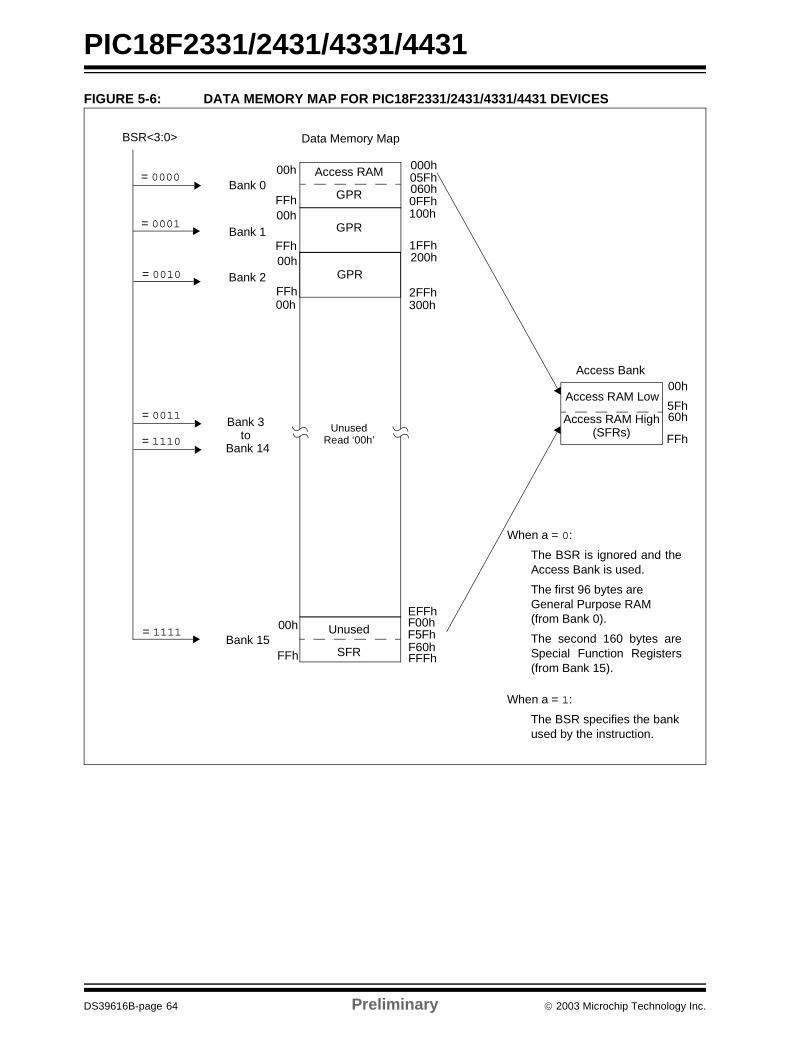
PIC18F2331/2431/4331/4431
FIGURE 5-6: DATA MEMORY MAP FOR PIC18F2331/2431/4331/4431 DEVICES
Bank 0
Bank 1
Bank 14
Bank 15
Data Memory MapBSR<3:0>
= 0000
= 0001
= 1111
060h05Fh
F60hFFFh
00h
5Fh60h
FFh
Access Bank
When a = 0:
The BSR is ignored and theAccess Bank is used.
The first 96 bytes are General Purpose RAM (from Bank 0).
The second 160 bytes areSpecial Function Registers(from Bank 15).
When a = 1:
The BSR specifies the bankused by the instruction.
F5FhF00hEFFh
1FFh
100h0FFh
000hAccess RAM
FFh
00h
FFh
00h
FFh
00h
GPR
GPR
SFR
Unused
Access RAM High
Access RAM Low
Bank 3to
200h
UnusedRead ‘00h’= 1110
= 0011
(SFRs)
= 0010 GPRFFh
00h
00h
Bank 2
300h2FFh
DS39616B-page 64 Preliminary 2003 Microchip Technology Inc.

PIC18F2331/2431/4331/4431
5.9.2 SPECIAL FUNCTION REGISTERS
The Special Function Registers (SFRs) are registersused by the CPU and Peripheral Modules for control-ling the desired operation of the device. These regis-ters are implemented as static RAM. A list of theseregisters is given in Table 5-1 and Table 5-2.
The SFRs can be classified into two sets; those asso-ciated with the “core” function and those related to theperipheral functions. Those registers related to the
“core” are described in this section, while those relatedto the operation of the peripheral features aredescribed in the section of that peripheral feature.
The SFRs are typically distributed among theperipherals whose functions they control.
The unused SFR locations will be unimplemented andread as ‘0’s.
TABLE 5-1: SPECIAL FUNCTION REGISTER MAP FOR PIC18F2331/2431/4331/4431 DEVICES
Address Name Address Name Address Name Address Name Address Name
FFFh TOSU FDFh INDF2 FBFh CCPR1H F9Fh IPR1 F7Fh PTCON0
FFEh TOSH FDEh POSTINC2 FBEh CCPR1L F9Eh PIR1 F7Eh PTCON1
FFDh TOSL FDDh POSTDEC2 FBDh CCP1CON F9Dh PIE1 F7Dh PTMRL
FFCh STKPTR FDCh PREINC2 FBCh CCPR2H F9Ch — F7Ch PTMRH
FFBh PCLATU FDBh PLUSW2 FBBh CCPR2L F9Bh OSCTUNE F7Bh PTPERL
FFAh PCLATH FDAh FSR2H FBAh CCP2CON F9Ah ADCON3 F7Ah PTPERH
FF9h PCL FD9h FSR2L FB9h ANSEL1 F99h ADCHS F79h PDC0L
FF8h TBLPTRU FD8h STATUS FB8h ANSEL0 F98h — F78h PDC0H
FF7h TBLPTRH FD7h TMR0H FB7h T5CON F97h — F77h PDC1L
FF6h TBLPTRL FD6h TMR0L FB6h QEICON F96h TRISE F76h PDC1H
FF5h TABLAT FD5h T0CON FB5h — F95h TRISD F75h PDC2L
FF4h PRODH FD4h — FB4h — F94h TRISC F74h PDC2H
FF3h PRODL FD3h OSCCON FB3h — F93h TRISB F73h PDC3L
FF2h INTCON FD2h LVDCON FB2h — F92h TRISA F72h PDC3H
FF1h INTCON2 FD1h WDTCON FB1h — F91h PR5H F71h SEVTCMPL
FF0h INTCON3 FD0h RCON FB0h SPBRGH F90h PR5L F70h SEVTCMPH
FEFh INDF0 FCFh TMR1H FAFh SPBRG F8Fh — F6Fh PWMCON0
FEEh POSTINC0 FCEh TMR1L FAEh RCREG F8Eh — F6Eh PWMCON1
FEDh POSTDEC0 FCDh T1CON FADh TXREG F8Dh LATE F6Dh DTCON
FECh PREINC0 FCCh TMR2 FACh TXSTA F8Ch LATD F6Ch FLTCONFIG
FEBh PLUSW0 FCBh PR2 FABh RCSTA F8Bh LATC F6Bh OVDCOND
FEAh FSR0H FCAh T2CON FAAh BAUDCTL F8Ah LATB F6Ah OVDCONS
FE9h FSR0L FC9h SSPBUF FA9h EEADR F89h LATA F69h CAP1BUFH
FE8h WREG FC8h SSPADD FA8h EEDATA F88h TMR5H F68h CAP1BUFL
FE7h INDF1 FC7h SSPSTAT FA7h EECON2 F87h TMR5L F67h CAP2BUFH
FE6h POSTINC1 FC6h SSPCON FA6h EECON1 F86h — F66h CAP2BUFL
FE5h POSTDEC1 FC5h — FA5h IPR3 F85h — F65h CAP3BUFH
FE4h PREINC1 FC4h ADRESH FA4h PIR3 F84h PORTE F64h CAP3BUFL
FE3h PLUSW1 FC3h ADRESL FA3h PIE3 F83h PORTD F63h CAP1CON
FE2h FSR1H FC2h ADCON0 FA2h IPR2 F82h PORTC F62h CAP2CON
FE1h FSR1L FC1h ADCON1 FA1h PIR2 F81h PORTB F61h CAP3CON
FE0h BSR FC0h ADCON2 FA0h PIE2 F80h PORTA F60h DFLTCON
2003 Microchip Technology Inc. Preliminary DS39616B-page 65

PIC18F2331/2431/4331/4431
TABLE 5-2: REGISTER FILE SUMMARY (PIC18F2331/2431/4331/4431)
File Name Bit 7 Bit 6 Bit 5 Bit 4 Bit 3 Bit 2 Bit 1 Bit 0 Value onPOR, BOR
Details on page:
TOSU — — — Top-of-Stack Upper Byte (TOS<20:16>) ---0 0000 48, 58
TOSH Top-of-Stack High Byte (TOS<15:8>) 0000 0000 48, 58
TOSL Top-of-Stack Low Byte (TOS<7:0>) 0000 0000 48, 58
STKPTR STKFUL STKUNF — Return Stack Pointer 00-0 0000 48, 59
PCLATU — — bit 21(3) Holding register for PC<20:16> ---0 0000 48, 60
PCLATH Holding register for PC<15:8> 0000 0000 48, 60
PCL PC Low Byte (PC<7:0>) 0000 0000 48, 60
TBLPTRU — — bit 21(3) Program Memory Table Pointer Upper Byte (TBLPTR<20:16>) --00 0000 48, 78
TBLPTRH Program Memory Table Pointer High Byte (TBLPTR<15:8>) 0000 0000 48, 78
TBLPTRL Program Memory Table Pointer Low Byte (TBLPTR<7:0>) 0000 0000 48, 78
TABLAT Program Memory Table Latch 0000 0000 48, 78
PRODH Product register High Byte xxxx xxxx 48, 89
PRODL Product register Low Byte xxxx xxxx 48, 89
INTCON GIE/GIEH PEIE/GIEL TMR0IE INT0IE RBIE TMR0IF INT0F RBIF 0000 000x 48, 93
INTCON2 RBPU INTEDG0 INTEDG1 INTEDG2 — TMR0IP — RBIP 1111 -1-1 48, 94
INTCON3 INT2P INT1P — INT2IE INT1IE — INT2IF INT1IF 11-0 0-00 48, 95
INDF0 Uses contents of FSR0 to address data memory – value of FSR0 not changed (not a physical register) N/A 48, 71
POSTINC0 Uses contents of FSR0 to address data memory – value of FSR0 post-incremented (not a physical register) N/A 48, 71
POSTDEC0 Uses contents of FSR0 to address data memory – value of FSR0 post-decremented (not a physical register) N/A 48, 71
PREINC0 Uses contents of FSR0 to address data memory – value of FSR0 pre-incremented (not a physical register) N/A 48, 71
PLUSW0 Uses contents of FSR0 to address data memory – value of FSR0 offset by W (not a physical register) N/A 48, 71
FSR0H — — — — Indirect Data Memory Address Pointer 0 High ---- 0000 48, 71
FSR0L Indirect Data Memory Address Pointer 0 Low Byte xxxx xxxx 48, 71
WREG Working register xxxx xxxx 48
INDF1 Uses contents of FSR1 to address data memory – value of FSR1 not changed (not a physical register) N/A 48, 71
POSTINC1 Uses contents of FSR1 to address data memory – value of FSR1 post-incremented (not a physical register) N/A 48, 71
POSTDEC1 Uses contents of FSR1 to address data memory – value of FSR1 post-decremented (not a physical register) N/A 48, 71
PREINC1 Uses contents of FSR1 to address data memory – value of FSR1 pre-incremented (not a physical register) N/A 48, 71
PLUSW1 Uses contents of FSR1 to address data memory – value of FSR1 offset by W (not a physical register) N/A 48, 71
FSR1H — — — — Indirect Data Memory Address Pointer 1 High ---- 0000 49, 71
FSR1L Indirect Data Memory Address Pointer 1 Low Byte xxxx xxxx 49, 71
BSR — — — — Bank Select Register ---- 0000 49, 70
INDF2 Uses contents of FSR2 to address data memory – value of FSR2 not changed (not a physical register) N/A 49, 71
POSTINC2 Uses contents of FSR2 to address data memory – value of FSR2 post-incremented (not a physical register) N/A 49, 71
POSTDEC2 Uses contents of FSR2 to address data memory – value of FSR2 post-decremented (not a physical register) N/A 49, 71
PREINC2 Uses contents of FSR2 to address data memory – value of FSR2 pre-incremented (not a physical register) N/A 49, 71
PLUSW2 Uses contents of FSR2 to address data memory – value of FSR2 offset by W (not a physical register) N/A 49, 71
FSR2H — — — — Indirect Data Memory Address Pointer 2 High ---- 0000 49, 71
FSR2L Indirect Data Memory Address Pointer 2 Low Byte xxxx xxxx 49, 71
STATUS — — — N OV Z DC C ---x xxxx 49, 73
TMR0H Timer0 register High Byte 0000 0000 49, 135
TMR0L Timer0 register Low Byte xxxx xxxx 49, 135
T0CON TMR0ON T016BIT — — T0PS3 T0PS2 T0PS1 T0PS0 11-- 1111 49, 133
Legend: x = unknown, u = unchanged, – = unimplemented, q = value depends on conditionNote 1: RA6 and associated bits are configured as port pins in RCIO, ECIO and INTIO2 (with port function on RA6) Oscillator mode only, and read
‘0’ in all other oscillator modes.2: RA7 and associated bits are configured as port pins in INTIO2 Oscillator mode only and read ‘0’ in all other modes.3: Bit 21 of the PC is only available in Test mode and serial programming modes.4: If PBADEN = 0, PORTB<4:0> are configured as digital input and read unknown, and if PBADEN = 1, PORTB<4:0> are configured as
analog input and read ‘0’ following a Reset.5: These registers and/or bits are not implemented on the PIC18F2X31 devices, and read as ‘0’.6: The RE3 port bit is only available when MCLRE fuse (CONFIG3H<7>) is programmed to ‘0’. Otherwise, RE3 reads ‘0’. This bit is read-only.
DS39616B-page 66 Preliminary 2003 Microchip Technology Inc.

PIC18F2331/2431/4331/4431
OSCCON IDLEN IRCF2 IRCF1 IRCF0 OSTS IOFS SCS1 SCS0 0000 q000 28, 49
LVDCON — — IVRST LVDEN LVDL3 LVDL2 LVDL1 LVDL0 --00 0101 49, 263
WDTCON WDTW — — — — — — SWDTEN 0000 0000 49, 279
RCON IPEN — — RI TO PD POR BOR 0--1 11qq 47, 74, 105
TMR1H Timer1 register High Byte xxxx xxxx 49, 141
TMR1L Timer1 register Low Byte xxxx xxxx 49, 141
T1CON RD16 T1RUN T1CKPS1 T1CKPS0 T1OSCEN T1SYNC TMR1CS TMR1ON 0000 0000 49, 137
TMR2 Timer2 register 0000 0000 49, 143
PR2 Timer2 Period register 1111 1111 49, 143
T2CON — TOUTPS3 TOUTPS2 TOUTPS1 TOUTPS0 TMR2ON T2CKPS1 T2CKPS0 -000 0000 49, 143
SSPBUF SSP Receive Buffer/Transmit register xxxx xxxx 49, 220
SSPADD SSP Address register in I2C Slave mode. SSP Baud Rate Reload register in I2C Master mode. 0000 0000 49, 220
SSPSTAT SMP CKE D/A P S R/W UA BF 0000 0000 49, 212
SSPCON WCOL SSPOV SSPEN CKP SSPM3 SSPM2 SSPM1 SSPM0 0000 0000 49, 213
ADRESH A/D Result register High Byte xxxx xxxx 50, 259
ADRESL A/D Result register Low Byte xxxx xxxx 50, 259
ADCON0 — — ACONV ACSCH ACMOD1 ACMOD0 GO/DONE ADON --00 0000 50, 244
ADCON1 VCFG1 VCFG0 — FIFOEN BFEMT FFOVFL ADPNT1 ADPNT0 00-0 1000 50, 245
ADCON2 ADFM ACQT3 ACQT2 ACQT1 ACQT0 ADCS2 ADCS1 ADCS0 0000 0000 50, 246
ADCON3 ADRS1 ADRS0 — SSRC4 SSRC3 SSRC2 SSRC1 SSRC0 00-0 0000 51. 247
ADCSH GDSEL1 GDSEL0 GBSEL1 GBSEL0 GCSEL1 GCSEL0 GASEL1 GASEL0 0000 0000 51, 248
CCPR1H Capture/Compare/PWM register1 High Byte xxxx xxxx 50, 152
CCPR1L Capture/Compare/PWM register1 Low Byte xxxx xxxx 50, 152
CCP1CON — — DC1B1 DC1B0 CCP1M3 CCP1M2 CCP1M1 CCP1M0 0000 0000 50, 155, 149
CCPR2H Capture/Compare/PWM register2 High Byte xxxx xxxx 50, 152
CCPR2L Capture/Compare/PWM register2 Low Byte xxxx xxxx 50, 152
CCP2CON — — DC2B1 DC2B0 CCP2M3 CCP2M2 CCP2M1 CCP2M0 --00 0000 50, 155
ANSEL1 — — — — — — — ANS8 ---- ---1 50, 249
ANSEL0 ANS7(6) ANS6(6) ANS5(6) ANS4 ANS3 ANS2 ANS1 ANS0 1111 1111 50, 249
T5CON T5SEN RESEN(5) T5MOD T5PS1 T5PS0 T5SYNC TMR5CS TMR5ON 0100 0000 50, 145
QEICON VELM ERROR UP/DOWN QEIM2 QEIM1 QEIM0 PDEC1 PDEC0 0000 0000 50, 171
SPBRGH Baud Rate Generator register, High Byte 0000 0000 50, 225
SPBRG USART Baud Rate Generator 0000 0000 50, 225
RCREG USART Receive register 0000 0000 50, 233, 232
TXREG USART Transmit register 0000 0000 50, 230, 232
TXSTA CSRC TX9 TXEN SYNC — BRGH TRMT TX9D 0000 -010 50, 222
RCSTA SPEN RX9 SREN CREN ADEN FERR OERR RX9D 0000 000x 50, 223
BAUDCTL — RCIDL — SCKP BRG16 — WUE ABDEN -1-1 0-00 50, 224
TABLE 5-2: REGISTER FILE SUMMARY (PIC18F2331/2431/4331/4431) (CONTINUED)
File Name Bit 7 Bit 6 Bit 5 Bit 4 Bit 3 Bit 2 Bit 1 Bit 0 Value onPOR, BOR
Details on page:
Legend: x = unknown, u = unchanged, – = unimplemented, q = value depends on conditionNote 1: RA6 and associated bits are configured as port pins in RCIO, ECIO and INTIO2 (with port function on RA6) Oscillator mode only, and read
‘0’ in all other oscillator modes.2: RA7 and associated bits are configured as port pins in INTIO2 Oscillator mode only and read ‘0’ in all other modes.3: Bit 21 of the PC is only available in Test mode and serial programming modes.4: If PBADEN = 0, PORTB<4:0> are configured as digital input and read unknown, and if PBADEN = 1, PORTB<4:0> are configured as
analog input and read ‘0’ following a Reset.5: These registers and/or bits are not implemented on the PIC18F2X31 devices, and read as ‘0’.6: The RE3 port bit is only available when MCLRE fuse (CONFIG3H<7>) is programmed to ‘0’. Otherwise, RE3 reads ‘0’. This bit is read-only.
2003 Microchip Technology Inc. Preliminary DS39616B-page 67

PIC18F2331/2431/4331/4431
EEADR EEPROM Address register 0000 0000 50, 85
EEDATA EEPROM Data register 0000 0000 50, 88
EECON2 EEPROM Control register2 (not a physical register) 0000 0000 50, 76, 85
EECON1 EEPGD CFGS — FREE WRERR WREN WR RD xx-0 x000 50, 77, 86
IPR3 — — — PTIP IC3DRIP IC2QEIP IC1IP TMR5IP ---1 1111 50
PIR3 — — — PTIF IC3DRIF IC2QEIF IC1IF TMR5IF ---0 0000 50
PIE3 — — — PTIE IC3DRIE IC2QEIE IC1IE TMR5IE ---0 0000 50
IPR2 OSFIP — — EEIP — LVDIP — CCP2IP 1--1 -1-1 51, 103
PIR2 OSFIF — — EEIF — LVDIF — CCP2IF 0--0 -0-0 51, 97
PIE2 OSFIE — — EEIE — LVDIE — CCP2IE 0--0 -0-0 51, 100
IPR1 — ADIP RCIP TXIP SSPIP CCP1IP TMR2IP TMR1IP -111 1111 51, 102
PIR1 — ADIF RCIF TXIF SSPIF CCP1IF TMR2IF TMR1IF -000 0000 51, 96
PIE1 — ADIE RCIE TXIE SSPIE CCP1IE TMR2IE TMR1IE -000 0000 51, 99
OSCTUNE — — TUN5 TUN4 TUN3 TUN2 TUN1 TUN0 --00 0000 25, 51
ADCON3 ADRS1 ADRS0 — SSRC4 SSRC3 SSRC2 SSRC1 SSRC0 00-0 0000 50
ADCHS GDSEL1 GDSEL0 GBSEL1 GBSEL0 GCSEL1 GCSEL0 GASEL1 GASEL0 0000 0000 50
TRISE(5) — — — — — Data Direction bits for PORTE(5) ---- -111 51, 131
TRISD(5) Data Direction Control register for PORTD 1111 1111 51, 128
TRISC Data Direction Control register for PORTC 1111 1111 51, 123
TRISB Data Direction Control register for PORTB 1111 1111 51, 117
TRISA TRISA7(2) TRISA6(1) Data Direction Control register for PORTA 1111 1111 51, 111
PR5H Timer5 Period register High Byte 1111 1111 50
PR5L Timer5 Period register Low Byte 1111 1111 50
LATE(5) — — — — — Read/Write PORTE Data Latch ---- -xxx 51, 132
LATD(5) Read/Write PORTD Data Latch xxxx xxxx 51, 128
LATC Read/Write PORTC Data Latch xxxx xxxx 51, 123
LATB Read/Write PORTB Data Latch xxxx xxxx 51, 117
LATA LATA<7>(2) LATA<6>(1) Read/Write PORTA Data Latch xxxx xxxx 51, 111
TMR5H Timer5 Timer register High Byte xxxx xxxx 146
TMR5L Timer5 Timer register Low Byte xxxx xxxx 146
PORTE — — — — RE3(6) Read PORTE pins,Write PORTE Data Latch(5)
---- xxxx 51, 132
PORTD Read PORTD pins, Write PORTD Data Latch xxxx xxxx 51, 128
PORTC Read PORTC pins, Write PORTC Data Latch xxxx xxxx 51, 123
PORTB Read PORTB pins, Write PORTB Data Latch(4) xxxx xxxx 51, 117
PORTA RA7(2) RA6(1) Read PORTA pins, Write PORTA Data Latch xx0x 0000 51, 111
PTCON0 PTOPS3 PTOPS2 PTOPS1 PTOPS0 PTCKPS1 PTCKPS0 PTMOD1 PTMOD0 0000 0000 52, 186
PTCON1 PTEN PTDIR — — — — — — 00-- ---- 52, 186
PTMRL PWM Time Base register (lower 8 bits). 0000 0000 184
PTMRH UNUSED PWM Time Base register (Upper 4 bits) ---- 0000 184
TABLE 5-2: REGISTER FILE SUMMARY (PIC18F2331/2431/4331/4431) (CONTINUED)
File Name Bit 7 Bit 6 Bit 5 Bit 4 Bit 3 Bit 2 Bit 1 Bit 0 Value onPOR, BOR
Details on page:
Legend: x = unknown, u = unchanged, – = unimplemented, q = value depends on conditionNote 1: RA6 and associated bits are configured as port pins in RCIO, ECIO and INTIO2 (with port function on RA6) Oscillator mode only, and read
‘0’ in all other oscillator modes.2: RA7 and associated bits are configured as port pins in INTIO2 Oscillator mode only and read ‘0’ in all other modes.3: Bit 21 of the PC is only available in Test mode and serial programming modes.4: If PBADEN = 0, PORTB<4:0> are configured as digital input and read unknown, and if PBADEN = 1, PORTB<4:0> are configured as
analog input and read ‘0’ following a Reset.5: These registers and/or bits are not implemented on the PIC18F2X31 devices, and read as ‘0’.6: The RE3 port bit is only available when MCLRE fuse (CONFIG3H<7>) is programmed to ‘0’. Otherwise, RE3 reads ‘0’. This bit is read-only.
DS39616B-page 68 Preliminary 2003 Microchip Technology Inc.

PIC18F2331/2431/4331/4431
PTPERL PWM Time Base Period register (Lower 8 bits). 1111 1111 184
PTPERH UNUSED PWM Time Base Period register (Upper 4 bits) ---- 1111 184
PDC0L PWM Duty Cycle #0L register (Lower 8 bits) --00 0000 184
PDC0H UNUSED PWM Duty Cycle #0H register (Upper 6 bits) 0000 0000 184
PDC1L PWM Duty Cycle #1L register (Lower 8 bits) 0000 0000 184
PDC1H UNUSED PWM Duty Cycle #1H register (Upper 6 bits) --00 0000 184
PDC2L PWM Duty Cycle #2L register (Lower 8 bits) 0000 0000 184
PDC2H UNUSED PWM Duty Cycle #2H register (Upper 6 bits) --00 0000 184
PDC3L PWM Duty Cycle #3L register (Lower 8 bits) 0000 0000 184
PDC3H UNUSED PWM Duty Cycle #3H register (Upper 6 bits) --00 0000 184
SEVTCMPL PWM Special Event Compare register (Lower 8 bits) 0000 0000 N/A
SEVTCMPH UNUSED PWM Special Event Compare reg (Upper 4 bits) ---- 0000 N/A
PWMCON0 — PWMEN2 PWMEN1 PWMEN0 PMOD3 PMOD2 PMOD1 PMOD0 -101 0000 52, 187
PWMCON1 SEVOPS3 SEVOPS2 SEVOPS1 SEVOPS0 SEVTDIR — UDIS OSYNC 0000 0-00 52, 188
DTCON DTPS1 DTPS0 DT5 DT4 DT3 DT2 DT1 DT0 0000 0000 52, 200
FLTCONFIG — FLTBS FLTBMOD FLTBEN FLTCON FLTAS FLTAMOD FLTAEN -000 0000 52, 208
OVDCOND POVD7 POVD6 POVD5 POVD4 POVD3 POVD2 POVD1 POVD0 1111 1111 52, 203
OVDCONS POUT7 POUT6 POUT5 POUT4 POUT3 POUT2 POUT1 POUT0 0000 0000 52, 204
CAP1BUFH/VELRH
Capture 1 register, High Byte/Velocity register, High Byte
xxxx xxxx 52,
CAP1BUFL/VELRL
Capture 1 register Low Byte/Velocity register, Low Byte
xxxx xxxx 52
CAP2BUFH/POSCNTH
Capture 2 register, High Byte/QEI Position Counter register, High Byte
xxxx xxxx 52
CAP2BUFL/POSCNTL
Capture 2 Reg., Low Byte/QEI Position Counter register, Low Byte
xxxx xxxx 52
CAP3BUFH/MAXCNTH
Capture 3 Reg., High Byte/QEI Max. Count Limit register, High Byte
xxxx xxxx 53
CAP3BUFL/MAXCNTL
Capture 3 Reg., Low Byte/QEI Max. Count Limit register, Low Byte
xxxx xxxx 53
CAP1CON — CAP1REN — — CAP1M3 CAP1M2 CAP1M1 CAP1M0 -0-0 0000 53, 163
CAP2CON — CAP2REN — — CAP2M3 CAP2M2 CAP2M1 CAP2M0 -0-0 0000 53, 163
CAP3CON — CAP3REN — — CAP3M3 CAP3M2 CAP3M1 CAP3M0 -0-0 0000 53, 163
DFLTCON — FLT4EN FLT3EN FLT2EN FLT1EN FLTCK2 FLTCK1 FLTCK0 -000 0000 53, 178
TABLE 5-2: REGISTER FILE SUMMARY (PIC18F2331/2431/4331/4431) (CONTINUED)
File Name Bit 7 Bit 6 Bit 5 Bit 4 Bit 3 Bit 2 Bit 1 Bit 0 Value onPOR, BOR
Details on page:
Legend: x = unknown, u = unchanged, – = unimplemented, q = value depends on conditionNote 1: RA6 and associated bits are configured as port pins in RCIO, ECIO and INTIO2 (with port function on RA6) Oscillator mode only, and read
‘0’ in all other oscillator modes.2: RA7 and associated bits are configured as port pins in INTIO2 Oscillator mode only and read ‘0’ in all other modes.3: Bit 21 of the PC is only available in Test mode and serial programming modes.4: If PBADEN = 0, PORTB<4:0> are configured as digital input and read unknown, and if PBADEN = 1, PORTB<4:0> are configured as
analog input and read ‘0’ following a Reset.5: These registers and/or bits are not implemented on the PIC18F2X31 devices, and read as ‘0’.6: The RE3 port bit is only available when MCLRE fuse (CONFIG3H<7>) is programmed to ‘0’. Otherwise, RE3 reads ‘0’. This bit is read-only.
2003 Microchip Technology Inc. Preliminary DS39616B-page 69

PIC18F2331/2431/4331/4431
5.10 Access Bank
The Access Bank is an architectural enhancementwhich is very useful for C compiler code optimization.The techniques used by the C compiler may also beuseful for programs written in assembly.
This data memory region can be used for:
• Intermediate computational values
• Local variables of subroutines• Faster context saving/switching of variables• Common variables
• Faster evaluation/control of SFRs (no banking)
The Access Bank is comprised of the last 128 bytes inBank 15 (SFRs) and the first 128 bytes in Bank 0.These two sections will be referred to as Access RAMHigh and Access RAM Low, respectively. Figure 5-6indicates the Access RAM areas.
A bit in the instruction word specifies if the operation isto occur in the bank specified by the BSR register or inthe Access Bank. This bit is denoted as the ‘a’ bit (foraccess bit).
When forced in the Access Bank (a = 0), the lastaddress in Access RAM Low is followed by the firstaddress in Access RAM High. Access RAM High mapsthe Special Function Registers, so these registers canbe accessed without any software overhead. This isuseful for testing status flags and modifying control bits.
5.11 Bank Select Register (BSR)
The need for a large general purpose memory spacedictates a RAM banking scheme. The data memory ispartitioned into as many as sixteen banks. When usingdirect addressing, the BSR should be configured for thedesired bank.
BSR<3:0> holds the upper 4 bits of the 12-bit RAMaddress. The BSR<7:4> bits will always read ‘0’s, andwrites will have no effect (see Figure 5-7).
A MOVLB instruction has been provided in theinstruction set to assist in selecting banks.
If the currently selected bank is not implemented, anyread will return all ‘0’s and all writes are ignored. TheStatus register bits will be set/cleared as appropriate forthe instruction performed.
Each Bank extends up to FFh (256 bytes). All datamemory is implemented as static RAM.
A MOVFF instruction ignores the BSR, since the 12-bitaddresses are embedded into the instruction word.
Section 5.12 “Indirect Addressing, INDF and FSRRegisters” provides a description of indirect address-ing, which allows linear addressing of the entire RAMspace.
FIGURE 5-7: DIRECT ADDRESSING
Note 1: For register file map detail, see Table 5-1.2: The access bit of the instruction can be used to force an override of the selected bank (BSR<3:0>) to the
registers of the Access Bank.3: The MOVFF instruction embeds the entire 12-bit address in the instruction.
DataMemory(1)
Direct Addressing
Bank Select(2) Location Select(3)
BSR<3:0> 7 0From Opcode(3)
00h 01h 0Eh 0Fh
Bank 0 Bank 1 Bank 14 Bank 15
1FFh
100h
0FFh
000h
EFFh
E00h
FFFh
F00h
BSR<7:4>
0 0 0 0
DS39616B-page 70 Preliminary 2003 Microchip Technology Inc.

PIC18F2331/2431/4331/4431
5.12 Indirect Addressing, INDF and FSR Registers
Indirect addressing is a mode of addressing data mem-ory, where the data memory address in the instructionis not fixed. An FSR register is used as a pointer to thedata memory location that is to be read or written. Sincethis pointer is in RAM, the contents can be modified bythe program. This can be useful for data tables in thedata memory and for software stacks. Figure 5-8shows how the fetched instruction is modified prior tobeing executed.
Indirect addressing is possible by using one of theINDF registers. Any instruction using the INDF registeractually accesses the register pointed to by the FileSelect Register, FSR. Reading the INDF register itself,indirectly (FSR = 0), will read 00h. Writing to the INDFregister indirectly, results in a no operation. The FSRregister contains a 12-bit address, which is shown inFigure 5-9.
The INDFn register is not a physical register. Address-ing INDFn actually addresses the register whoseaddress is contained in the FSRn register (FSRn is apointer). This is indirect addressing.
Example 5-5 shows a simple use of indirect addressingto clear the RAM in Bank 1 (locations 100h-1FFh) in aminimum number of instructions.
EXAMPLE 5-5: HOW TO CLEAR RAM (BANK 1) USING INDIRECT ADDRESSING
There are three indirect addressing registers. Toaddress the entire data memory space (4096 bytes),these registers are 12-bits wide. To store the 12 bits ofaddressing information, two 8-bit registers arerequired:
1. FSR0: composed of FSR0H:FSR0L2. FSR1: composed of FSR1H:FSR1L3. FSR2: composed of FSR2H:FSR2L
In addition, there are registers INDF0, INDF1 andINDF2, which are not physically implemented. Readingor writing to these registers activates indirect address-ing, with the value in the corresponding FSR registerbeing the address of the data. If an instruction writes avalue to INDF0, the value will be written to the addresspointed to by FSR0H:FSR0L. A read from INDF1 readsthe data from the address pointed to byFSR1H:FSR1L. INDFn can be used in code anywherean operand can be used.
If INDF0, INDF1 or INDF2 are read indirectly via a FSR,all ‘0’s are read (zero bit is set). Similarly, if INDF0,INDF1 or INDF2 are written to indirectly, the operationwill be equivalent to a NOP instruction and the Statusbits are not affected.
5.12.1 INDIRECT ADDRESSING OPERATION
Each FSR register has an INDF register associatedwith it, plus four additional register addresses. Perform-ing an operation using one of these five registers deter-mines how the FSR will be modified during indirectaddressing.
When data access is performed using one of the fiveINDFn locations, the address selected will configurethe FSRn register to:
• Do nothing to FSRn after an indirect access (no change) – INDFn
• Auto-decrement FSRn after an indirect access (post-decrement) – POSTDECn
• Auto-increment FSRn after an indirect access (post-increment) – POSTINCn
• Auto-increment FSRn before an indirect access (pre-increment) – PREINCn
• Use the value in the WREG register as an offset to FSRn. Do not modify the value of the WREG or the FSRn register after an indirect access (no change) – PLUSWn
When using the auto-increment or auto-decrement fea-tures, the effect on the FSR is not reflected in the Statusregister. For example, if the indirect address causes theFSR to equal ‘0’, the Z bit will not be set.
Auto-incrementing or auto-decrementing a FSR affectsall 12 bits. That is, when FSRnL overflows from anincrement, FSRnH will be incremented automatically.
Adding these features allows the FSRn to be used as astack pointer, in addition to its uses for table operationsin data memory.
Each FSR has an address associated with it that per-forms an indexed indirect access. When a data accessto this INDFn location (PLUSWn) occurs, the FSRn isconfigured to add the signed value in the WREG regis-ter and the value in FSR to form the address before anindirect access. The FSR value is not changed. TheWREG offset range is -128 to +127.
If an FSR register contains a value that points to one ofthe INDFn, an indirect read will read 00h (zero bit isset), while an indirect write will be equivalent to a NOP(Status bits are not affected).
If an indirect addressing write is performed when thetarget address is an FSRnH or FSRnL register, the datais written to the FSR register, but no pre- or post-increment/decrement is performed.
LFSR FSR0, 0x100; NEXT CLRF POSTINC0 ; Clear INDF
; register then ; inc pointer
BTFSS FSR0H, 1 ; All done with; Bank1?
GOTO NEXT ; NO, clear next CONTINUE ; YES, continue
2003 Microchip Technology Inc. Preliminary DS39616B-page 71

PIC18F2331/2431/4331/4431
FIGURE 5-8: INDIRECT ADDRESSING OPERATION
FIGURE 5-9: INDIRECT ADDRESSING
Opcode Address
File Address = access of an indirect addressing register
FSR
InstructionExecuted
InstructionFetched
RAM
Opcode File
1212
12
BSR<3:0>
84
0h
FFFh
Note 1: For register file map detail, see Table 5-1.
DataMemory(1)
Indirect AddressingFSRnH:FSRnL
3 0
0FFFh
0000h
Location Select
11 0
0 7
DS39616B-page 72 Preliminary 2003 Microchip Technology Inc.

PIC18F2331/2431/4331/4431
5.13 Status Register
The Status register, shown in Register 5-2, contains thearithmetic status of the ALU. The Status register can bethe operand for any instruction, as with any other reg-ister. If the Status register is the destination for aninstruction that affects the Z, DC, C, OV or N bits, thenthe write to these five bits is disabled. These bits are setor cleared according to the device logic. Therefore, theresult of an instruction with the Status register as desti-nation may be different than intended.
For example, CLRF STATUS will clear the upper threebits and set the Z bit. This leaves the Status register as000u u1uu (where u = unchanged).
It is recommended, therefore, that only BCF, BSF,SWAPF, MOVFF and MOVWF instructions are used toalter the Status register, because these instructions donot affect the Z, C, DC, OV or N bits in the Status reg-ister. For other instructions not affecting any status bits,see Table 23-2.
REGISTER 5-2: STATUS REGISTER
Note: The C and DC bits operate as a borrowand digit borrow bit respectively, in sub-traction.
U-0 U-0 U-0 R/W-x R/W-x R/W-x R/W-x R/W-x
— — — N OV Z DC C
bit 7 bit 0
bit 7-5 Unimplemented: Read as ‘0’
bit 4 N: Negative bit This bit is used for signed arithmetic (2’s complement). It indicates whether the result was negative (ALU MSB = 1).1 = Result was negative 0 = Result was positive
bit 3 OV: Overflow bit This bit is used for signed arithmetic (2’s complement). It indicates an overflow of the 7-bit magnitude, which causes the sign bit (bit7) to change state.1 = Overflow occurred for signed arithmetic (in this arithmetic operation) 0 = No overflow occurred
bit 2 Z: Zero bit 1 = The result of an arithmetic or logic operation is zero 0 = The result of an arithmetic or logic operation is not zero
bit 1 DC: Digit carry/borrow bit For ADDWF, ADDLW, SUBLW and SUBWF instructions 1 = A carry-out from the 4th low order bit of the result occurred 0 = No carry-out from the 4th low order bit of the result
Note: For borrow, the polarity is reversed. A subtraction is executed by adding the2’s complement of the second operand. For rotate (RRF, RLF) instructions, thisbit is loaded with either the bit 4 or bit 3 of the source register.
bit 0 C: Carry/borrow bit For ADDWF, ADDLW, SUBLW and SUBWF instructions 1 = A carry-out from the Most Significant bit of the result occurred 0 = No carry-out from the Most Significant bit of the result occurred
Note: For borrow, the polarity is reversed. A subtraction is executed by adding the2’s complement of the second operand. For rotate (RRF, RLF) instructions, thisbit is loaded with either the high- or low-order bit of the source register.
Legend:
R = Readable bit W = Writable bit U = Unimplemented bit, read as ‘0’
- n = Value at POR ‘1’ = Bit is set ‘0’ = Bit is cleared x = Bit is unknown
2003 Microchip Technology Inc. Preliminary DS39616B-page 73

PIC18F2331/2431/4331/4431
5.14 RCON Register
The Reset Control (RCON) register contains flag bitsthat allow differentiation between the sources of adevice Reset. These flags include the TO, PD, POR,BOR and RI bits. This register is readable and writable.
REGISTER 5-3: RCON REGISTER
Note 1: If the BOREN configuration bit is set(Brown-out Reset enabled), the BOR bitis ‘1’ on a Power-on Reset. After a Brown-out Reset has occurred, the BOR bit willbe cleared and must be set by firmware toindicate the occurrence of the nextBrown-out Reset.
2: It is recommended that the POR bit be setafter a Power-on Reset has beendetected, so that subsequent Power-onResets may be detected.
R/W-0 U-0 U-0 R/W-1 R-1 R-1 R/W-0 R/W-0
IPEN — — RI TO PD POR BOR
bit 7 bit 0
bit 7 IPEN: Interrupt Priority Enable bit 1 = Enable priority levels on interrupts0 = Disable priority levels on interrupts (PIC16CXXX Compatibility mode)
bit 6-5 Unimplemented: Read as ‘0’
bit 4 RI: RESET Instruction Flag bit1 = The RESET instruction was not executed (set by firmware only)0 = The RESET instruction was executed causing a device Reset
(must be set in firmware after a Brown-out Reset occurs)
bit 3 TO: Watchdog Time-out Flag bit
1 = Set by power-up, CLRWDT instruction, or SLEEP instruction 0 = A WDT time-out occurred
bit 2 PD: Power-down Detection Flag bit 1 = Set by power-up or by the CLRWDT instruction 0 = Cleared by execution of the SLEEP instruction
bit 1 POR: Power-on Reset Status bit 1 = A Power-on Reset has not occurred (set by firmware only)0 = A Power-on Reset occurred
(must be set in firmware after a Power-on Reset occurs)
bit 0 BOR: Brown-out Reset Status bit1 = A Brown-out Reset has not occurred (set by firmware only)0 = A Brown-out Reset occurred
(must be set in firmware after a Brown-out Reset occurs)
Legend:
R = Readable bit W = Writable bit U = Unimplemented bit, read as ‘0’
- n = Value at POR ‘1’ = Bit is set ‘0’ = Bit is cleared x = Bit is unknown
DS39616B-page 74 Preliminary 2003 Microchip Technology Inc.

PIC18F2331/2431/4331/4431
6.0 FLASH PROGRAM MEMORY
The Flash program memory is readable, writable anderasable during normal operation over the entire VDD
range.
A read from program memory is executed on one byteat a time. A write to program memory is executed onblocks of 8 bytes at a time. Program memory is erasedin blocks of 64 bytes at a time. A bulk erase operationmay not be issued from user code.
While writing or erasing program memory, instructionfetches cease until the operation is complete. Theprogram memory cannot be accessed during the writeor erase, therefore, code cannot execute. An internalprogramming timer terminates program memory writesand erases.
A value written to program memory does not need to bea valid instruction. Executing a program memorylocation that forms an invalid instruction results in aNOP.
6.1 Table Reads and Table Writes
In order to read and write program memory, there aretwo operations that allow the processor to move bytesbetween the program memory space and the dataRAM:
• Table Read (TBLRD)• Table Write (TBLWT)
The program memory space is 16-bits wide, while thedata RAM space is 8-bits wide. Table reads and tablewrites move data between these two memory spacesthrough an 8-bit register (TABLAT).
Table read operations retrieve data from programmemory and place it into TABLAT in the data RAMspace. Figure 6-1 shows the operation of a table readwith program memory and data RAM.
Table write operations store data from TABLAT in thedata memory space into holding registers in programmemory. The procedure to write the contents of theholding registers into program memory is detailed inSection 6.5 “Writing to Flash Program Memory”.Figure 6-2 shows the operation of a table write withprogram memory and data RAM.
Table operations work with byte entities. A table blockcontaining data, rather than program instructions, is notrequired to be word aligned. Therefore, a table blockcan start and end at any byte address. If a table write isbeing used to write executable code into programmemory, program instructions will need to be wordaligned, (TBLPTRL<0> = 0).
The EEPROM on-chip timer controls the write anderase times. The write and erase voltages are gener-ated by an on-chip charge pump rated to operate overthe voltage range of the device for byte or wordoperations.
FIGURE 6-1: TABLE READ OPERATION
Table Pointer(1)
Table Latch (8-bit)Program Memory
TBLPTRH TBLPTRLTABLAT
TBLPTRU
Instruction: TBLRD*
Note 1: Table Pointer points to a byte in program memory.
Program Memory(TBLPTR)
2003 Microchip Technology Inc. Preliminary DS39616B-page 75

PIC18F2331/2431/4331/4431
FIGURE 6-2: TABLE WRITE OPERATION
6.2 Control Registers
Several control registers are used in conjunction withthe TBLRD and TBLWT instructions. These include the:
• EECON1 register• EECON2 register• TABLAT register
• TBLPTR registers
6.2.1 EECON1 AND EECON2 REGISTERS
EECON1 is the control register for memory accesses.
EECON2 is not a physical register. Reading EECON2will read all ‘0’s. The EECON2 register is usedexclusively in the memory write and erase sequences.
Control bit EEPGD determines if the access will be toprogram or data EEPROM memory. When clear, oper-ations will access the data EEPROM memory. Whenset, program memory is accessed.
Control bit CFGS determines if the access will be to theconfiguration registers or to program memory/dataEEPROM memory. When set, subsequent operationsaccess configuration registers. When CFGS is clear,the EEPGD bit selects either program Flash or dataEEPROM memory.
The FREE bit controls program memory erase opera-tions. When the FREE bit is set, the erase operation isinitiated on the next WR command. When FREE isclear, only writes are enabled.
The WREN bit enables and disables erase and writeoperations. When set, erase and write operations areallowed. When clear, erase and write operations aredisabled – the WR bit cannot be set while the WREN bitis clear. This process helps to prevent accidental writesto memory due to errant (unexpected) code execution.
Firmware should keep the WREN bit clear at all times,except when starting erase or write operations. Oncefirmware has set the WR bit, the WREN bit may becleared. Clearing the WREN bit will not affect theoperation in progress.
The WRERR bit is set when a write operation is inter-rupted by a Reset. In these situations, the user cancheck the WRERR bit and rewrite the location. It will benecessary to reload the data and address registers(EEDATA and EEADR) as these registers have clearedas a result of the Reset.
Control bits RD and WR start read and erase/writeoperations, respectively. These bits are set by firm-ware, and cleared by hardware at the completion of theoperation.
The RD bit cannot be set when accessing programmemory (EEPGD = 1). Program memory is read usingtable read instructions. See Section 6.3 “Reading theFlash Program Memory” regarding table reads.
Table Pointer(1)Table Latch (8-bit)
TBLPTRH TBLPTRL TABLAT
Program Memory(TBLPTR)
TBLPTRU
Instruction: TBLWT*
Note 1: Table Pointer actually points to one of eight holding registers, the address of which is determined byTBLPTRL<2:0>. The process for physically writing data to the Program Memory Array is discussed inSection 6.5 “Writing to Flash Program Memory”.
Holding Registers Program Memory
Note: Interrupt flag bit EEIF, in the PIR2 register,is set when the write is complete. It mustbe cleared in software.
DS39616B-page 76 Preliminary 2003 Microchip Technology Inc.

PIC18F2331/2431/4331/4431
REGISTER 6-1: EECON1 REGISTER R/W-x R/W-x U-0 R/W-0 R/W-x R/W-0 R/S-0 R/S-0
EEPGD CFGS — FREE WRERR WREN WR RD
bit 7 bit 0
bit 7 EEPGD: Flash Program or Data EEPROM Memory Select bit1 = Access program Flash memory0 = Access data EEPROM memory
bit 6 CFGS: Flash Program/Data EE or Configuration Select bit
1 = Access configuration registers0 = Access program Flash or data EEPROM memory
bit 5 Unimplemented: Read as ‘0’
bit 4 FREE: Flash Row Erase Enable bit1 = Erase the program memory row addressed by TBLPTR on the next WR command
(cleared by completion of erase operation – TBLPTR<5:0> are ignored)0 = Perform write only
bit 3 WRERR: EEPROM Error Flag bit1 = A write operation was prematurely terminated (any Reset during self-timed
programming)0 = The write operation completed normally
Note: When a WRERR occurs, the EEPGD and CFGS bits are not cleared. This allows tracing of the error condition.
bit 2 WREN: Write Enable bit1 = Allows erase or write cycles0 = Inhibits erase or write cycles
bit 1 WR: Write Control bit1 = Initiates a data EEPROM erase/write cycle or a program memory erase cycle or write
cycle. (The operation is self-timed and the bit is cleared by hardware once write is complete. TheWR bit can only be set (not cleared) in software.)
0 = Write cycle completed
bit 0 RD: Read Control bit
1 = Initiates a memory read (Read takes one cycle. RD is cleared in hardware. The RD bit can only be set (not cleared)in software. RD bit cannot be set when EEPGD = 1.)
0 = Read completed
Legend:
R = Readable bit S = Settable only U = Unimplemented bit, read as ‘0’
W = Writable bit - n = Value at POR ‘1’ = Bit is set ‘0’ = Bit is cleared
x = Bit is unknown
2003 Microchip Technology Inc. Preliminary DS39616B-page 77

PIC18F2331/2431/4331/4431
6.2.2 TABLAT – TABLE LATCH REGISTER
The Table Latch (TABLAT) is an 8-bit register mappedinto the SFR space. The Table Latch is used to hold8-bit data during data transfers between programmemory and data RAM.
6.2.3 TBLPTR – TABLE POINTER REGISTER
The Table Pointer (TBLPTR) addresses a byte withinthe program memory. The TBLPTR is comprised ofthree SFR registers: Table Pointer Upper Byte, TablePointer High Byte and Table Pointer Low Byte(TBLPTRU:TBLPTRH:TBLPTRL). These three regis-ters join to form a 22-bit wide pointer. The low order 21bits allow the device to address up to 2 Mbytes of pro-gram memory space. Setting the 22nd bit allowsaccess to the Device ID, the User ID and theConfiguration bits.
The TBLPTR is used by the TBLRD and TBLWT instruc-tions. These instructions can update the TBLPTR inone of four ways based on the table operation. Theseoperations are shown in Table 6-1. These operationson the TBLPTR only affect the low order 21 bits.
6.2.4 TABLE POINTER BOUNDARIES
TBLPTR is used in reads, writes and erases of theFlash program memory.
When a TBLRD is executed, all 22 bits of the TablePointer determine which byte is read from program orconfiguration memory into TABLAT.
When a TBLWT is executed, the three LSbs of the TablePointer (TBLPTR<2:0>) determine which of the eightprogram memory holding registers is written to. Whenthe timed write to program memory (long write) begins,the 19 MSbs of the Table Pointer, TBLPTR(TBLPTR<21:3>), will determine which programmemory block of 8 bytes is written to (TBLPTR<2:0>are ignored). For more detail, see Section 6.5“Writing to Flash Program Memory”.
When an erase of program memory is executed, the 16MSbs of the Table Pointer (TBLPTR<21:6>) point to the64-byte block that will be erased. The Least Significantbits (TBLPTR<5:0>) are ignored.
Figure 6-3 describes the relevant boundaries ofTBLPTR based on Flash program memory operations.
TABLE 6-1: TABLE POINTER OPERATIONS WITH TBLRD AND TBLWT INSTRUCTIONS
FIGURE 6-3: TABLE POINTER BOUNDARIES BASED ON OPERATION
Example Operation on Table Pointer
TBLRD*TBLWT*
TBLPTR is not modified
TBLRD*+TBLWT*+
TBLPTR is incremented after the read/write
TBLRD*-TBLWT*-
TBLPTR is decremented after the read/write
TBLRD+*TBLWT+*
TBLPTR is incremented before the read/write
21 16 15 8 7 0
ERASE – TBLPTR<21:6>
LONG WRITE – TBLPTR<21:3>
READ or WRITE – TBLPTR<21:0>
TBLPTRLTBLPTRHTBLPTRU
DS39616B-page 78 Preliminary 2003 Microchip Technology Inc.

PIC18F2331/2431/4331/4431
6.3 Reading the Flash Program Memory
The TBLRD instruction is used to retrieve data fromprogram memory and placed into data RAM. Tablereads from program memory are performed one byte ata time.
TBLPTR points to a byte address in program space.Executing a TBLRD instruction places the byte pointedto into TABLAT. In addition, TBLPTR can be modifiedautomatically for the next table read operation.
The internal program memory is typically organized bywords. The Least Significant bit of the address selectsbetween the high and low bytes of the word. Figure 6-4shows the interface between the internal programmemory and the TABLAT.
FIGURE 6-4: READS FROM FLASH PROGRAM MEMORY
EXAMPLE 6-1: READING A FLASH PROGRAM MEMORY WORD
Odd (High) Byte
Program Memory
Even (Low) Byte
TABLAT
TBLPTR
Instruction Register (IR) Read Register
LSB = 1TBLPTRLSB = 0
MOVLW CODE_ADDR_UPPER ; Load TBLPTR with the baseMOVWF TBLPTRU ; address of the wordMOVLW CODE_ADDR_HIGHMOVWF TBLPTRHMOVLW CODE_ADDR_LOWMOVWF TBLPTRL
READ_WORDTBLRD*+ ; read into TABLAT and increment TBLPTRMOVFW TABLAT ; get dataMOVWF WORD_EVENTBLRD*+ ; read into TABLAT and increment TBLPTRMOVFW TABLAT ; get dataMOVWF WORD_ODD
2003 Microchip Technology Inc. Preliminary DS39616B-page 79

PIC18F2331/2431/4331/4431
6.4 Erasing Flash Program Memory
The minimum erase block size is 32 words or 64 bytesunder firmware control. Only through the use of anexternal programmer, or through ICSP control canlarger blocks of program memory be bulk erased. Worderase in Flash memory is not supported.
When initiating an erase sequence from the micro-controller itself, a block of 64 bytes of program memoryis erased. The Most Significant 16 bits of theTBLPTR<21:6> point to the block being erased.TBLPTR<5:0> are ignored.
The EECON1 register commands the erase operation.The EEPGD bit must be set to point to the Flash pro-gram memory. The CFGS bit must be clear to accessprogram Flash and data EEPROM memory. TheWREN bit must be set to enable write operations. TheFREE bit is set to select an erase operation. The WRbit is set as part of the required instruction sequence(as shown in Example 6-2), and starts the actual eraseoperation. It is not necessary to load the TABLATregister with any data, as it is ignored.
For protection, the write initiate sequence usingEECON2 must be used.
A long write is necessary for erasing the internal Flash.Instruction execution is halted while in a long writecycle. The long write will be terminated by the internalprogramming timer.
6.4.1 FLASH PROGRAM MEMORY ERASE SEQUENCE
The sequence of events for erasing a block of internalprogram memory location is:
1. Load table pointer with address of row beingerased.
2. Set the EECON1 register for the eraseoperation:- set EEPGD bit to point to program
memory;- clear the CFGS bit to access program
memory;- set WREN bit to enable writes;- set FREE bit to enable the erase.
3. Disable interrupts.4. Write 55h to EECON2.5. Write AAh to EECON2.
6. Set the WR bit. This will begin the row erasecycle.
7. The CPU will stall for duration of the erase(about 2 ms using internal timer).
8. Execute a NOP.9. Re-enable interrupts.
EXAMPLE 6-2: ERASING A FLASH PROGRAM MEMORY ROW MOVLW CODE_ADDR_UPPER ; load TBLPTR with the baseMOVWF TBLPTRU ; address of the memory blockMOVLW CODE_ADDR_HIGHMOVWF TBLPTRH MOVLW CODE_ADDR_LOWMOVWF TBLPTRL
ERASE_ROW BSF EECON1,EEPGD ; point to Flash program memoryBSF EECON1,WREN ; enable write to memoryBSF EECON1,FREE ; enable Row Erase operationBCF INTCON,GIE ; disable interruptsMOVLW 55hMOVWF EECON2 ; write 55H
Required MOVLW AAhSequence MOVWF EECON2 ; write AAH
BSF EECON2,WR ; start erase (CPU stall)NOPBSF INTCON,GIE ; re-enable interrupts
DS39616B-page 80 Preliminary 2003 Microchip Technology Inc.

PIC18F2331/2431/4331/4431
6.5 Writing to Flash Program Memory
The programming block size is 4 words or 8 bytes.Word or byte programming is not supported.
Table writes are used internally to load the holdingregisters needed to program the Flash memory. Thereare 8 holding registers used by the table writes forprogramming.
Since the Table Latch (TABLAT) is only a single byte,the TBLWT instruction has to be executed 8 times foreach programming operation. All of the table writeoperations will essentially be short writes, because onlythe holding registers are written. At the end of updating8 registers, the EECON1 register must be written to, tostart the programming operation with a long write.
The long write is necessary for programming theinternal Flash. Instruction execution is halted while in along write cycle. The long write will be terminated bythe internal programming timer.
FIGURE 6-5: TABLE WRITES TO FLASH PROGRAM MEMORY
6.5.1 FLASH PROGRAM MEMORY WRITE SEQUENCE
The sequence of events for programming an internalprogram memory location should be:
1. Read 64 bytes into RAM.2. Update data values in RAM as necessary.3. Load Table Pointer with address being erased.
4. Do the row erase procedure (see Section 6.4.1“Flash Program Memory Erase Sequence”).
5. Load Table Pointer with address of first bytebeing written.
6. Write the first 8 bytes into the holding registerswith auto-increment.
7. Set the EECON1 register for the write operation:- set EEPGD bit to point to program
memory;- clear the CFGS bit to access program
memory;- set WREN bit to enable byte writes.
8. Disable interrupts.
9. Write 55h to EECON2.
10. Write AAh to EECON2.11. Set the WR bit. This will begin the write cycle.12. The CPU will stall for duration of the write (about
2 ms using internal timer).13. Execute a NOP.
14. Re-enable interrupts.15. Repeat steps 6-14 seven times, to write 64
bytes.16. Verify the memory (table read).
This procedure will require about 18 ms to update onerow of 64 bytes of memory. An example of the requiredcode is given in Example 6-3.
Holding Register
TABLAT
Holding Register
TBLPTR = xxxxx7
Holding Register
TBLPTR = xxxxx1
Holding Register
TBLPTR = xxxxx0
8 8 8 8
Write Register
TBLPTR = xxxxx2
Program Memory
2003 Microchip Technology Inc. Preliminary DS39616B-page 81

PIC18F2331/2431/4331/4431
EXAMPLE 6-3: WRITING TO FLASH PROGRAM MEMORYMOVLW D'64 ; number of bytes in erase blockMOVWF COUNTERMOVLW BUFFER_ADDR_HIGH ; point to bufferMOVWF FSR0HMOVLW BUFFER_ADDR_LOWMOVWF FSR0LMOVLW CODE_ADDR_UPPER ; Load TBLPTR with the baseMOVWF TBLPTRU ; address of the memory blockMOVLW CODE_ADDR_HIGHMOVWF TBLPTRHMOVLW CODE_ADDR_LOW ; 6 LSB = 0MOVWF TBLPTRL
READ_BLOCKTBLRD*+ ; read into TABLAT, and incMOVFW TABLAT ; get dataMOVWF POSTINC0 ; store data and increment FSR0DECFSZ COUNTER ; done?GOTO READ_BLOCK ; repeat
MODIFY_WORDMOVLW DATA_ADDR_HIGH ; point to bufferMOVWF FSR0HMOVLW DATA_ADDR_LOWMOVWF FSR0LMOVLW NEW_DATA_LOW ; update buffer word and increment FSR0MOVWF POSTINC0MOVLW NEW_DATA_HIGH ; update buffer wordMOVWF INDF0
ERASE_BLOCKMOVLW CODE_ADDR_UPPER ; load TBLPTR with the baseMOVWF TBLPTRU ; address of the memory blockMOVLW CODE_ADDR_HIGHMOVWF TBLPTRH MOVLW CODE_ADDR_LOW ; 6 LSB = 0MOVWF TBLPTRLBCF EECON1,CFGS ; point to PROG/EEPROM memory BSF EECON1,EEPGD ; point to Flash program memoryBSF EECON1,WREN ; enable write to memoryBSF EECON1,FREE ; enable Row Erase operationBCF INTCON,GIE ; disable interruptsMOVLW 55h ; Required sequenceMOVWF EECON2 ; write 55HMOVLW AAhMOVWF EECON2 ; write AAHBSF EECON1,WR ; start erase (CPU stall)NOPBSF INTCON,GIE ; re-enable interrupts
WRITE_BUFFER_BACKMOVLW 8 ; number of write buffer groups of 8 bytesMOVWF COUNTER_HIMOVLW BUFFER_ADDR_HIGH ; point to bufferMOVWF FSR0HMOVLW BUFFER_ADDR_LOWMOVWF FSR0L
PROGRAM_LOOPMOVLW 8 ; number of bytes in holding registerMOVWF COUNTER
WRITE_WORD_TO_HREGSMOVFW POSTINC0 ; get low byte of buffer data and increment FSR0MOVWF TABLAT ; present data to table latchTBLWT+* ; short write
; to internal TBLWT holding register, increment; TBLPTR
DECFSZ COUNTER ; loop until buffers are fullGOTO WRITE_WORD_TO_HREGS
DS39616B-page 82 Preliminary 2003 Microchip Technology Inc.

PIC18F2331/2431/4331/4431
EXAMPLE 6-3: WRITING TO FLASH PROGRAM MEMORY (CONTINUED)
6.5.2 WRITE VERIFY
Depending on the application, good programmingpractice may dictate that the value written to thememory should be verified against the original value.This should be used in applications where excessivewrites can stress bits near the specification limit.
6.5.3 UNEXPECTED TERMINATION OF WRITE OPERATION
If a write is terminated by an unplanned event, such asloss of power or an unexpected Reset, the memorylocation just programmed should be verified and repro-grammed if needed. The WRERR bit is set when awrite operation is interrupted by a MCLR Reset, or aWDT Time-out Reset during normal operation. In thesesituations, users can check the WRERR bit and rewritethe location.
6.6 Flash Program Operation During Code Protection
See Section 22.5 “Program Verification and CodeProtection” for details on code protection of Flash pro-gram memory.
TABLE 6-2: REGISTERS ASSOCIATED WITH PROGRAM FLASH MEMORY
PROGRAM_MEMORYBCF INTCON,GIE ; disable interruptsMOVLW 55h ; required sequenceMOVWF EECON2 ; write 55HMOVLW AAhMOVWF EECON2 ; write AAHBSF EECON1,WR ; start program (CPU stall)NOPBSF INTCON, GIE ; re-enable interruptsDECFSZ COUNTER_HI ; loop until doneGOTO PROGRAM_LOOPBCF EECON1, WREN ; disable write to memory
Name Bit 7 Bit 6 Bit 5 Bit 4 Bit 3 Bit 2 Bit 1 Bit 0Value on:POR, BOR
Value on all other Resets
TBLPTRU — — bit21 Program Memory Table Pointer Upper Byte (TBLPTR<20:16>)
--00 0000 --00 0000
TBPLTRH Program Memory Table Pointer High Byte (TBLPTR<15:8>) 0000 0000 0000 0000
TBLPTRL Program Memory Table Pointer High Byte (TBLPTR<7:0>) 0000 0000 0000 0000
TABLAT Program Memory Table Latch 0000 0000 0000 0000
INTCON GIE/GIEH PEIE/GIEL TMR0IE INT0IE RBIE TMR0IF INTF RBIF 0000 000x 0000 000u
EECON2 EEPROM Control Register2 (not a physical register) — —
EECON1 EEPGD CFGS — FREE WRERR WREN WR RD xx-0 x000 uu-0 u000
IPR2 OSFIP — — EEIP — LVDIP — CCP2IP 1--1 -1-1 1--1 -1-1
PIR2 OSFIF — — EEIF — LVDIF — CCP2IF 0--0 -0-0 0--0 -0-0
PIE2 OSFIE — — EEIE — LVDIE — CCP2IE 0--0 -0-0 0--0 -0-0
Legend: x = unknown, u = unchanged, r = reserved, - = unimplemented, read as ‘0’. Shaded cells are not used during Flash/EEPROM access.
2003 Microchip Technology Inc. Preliminary DS39616B-page 83

PIC18F2331/2431/4331/4431
NOTES:
DS39616B-page 84 Preliminary 2003 Microchip Technology Inc.

PIC18F2331/2431/4331/4431
7.0 DATA EEPROM MEMORY
The Data EEPROM is readable and writable duringnormal operation over the entire VDD range. The datamemory is not directly mapped in the register filespace. Instead, it is indirectly addressed through theSpecial Function Registers (SFR).
There are four SFRs used to read and write theprogram and data EEPROM memory. These registersare:
• EECON1• EECON2• EEDATA
• EEADR
The EEPROM data memory allows byte read and write.When interfacing to the data memory block, EEDATAholds the 8-bit data for read/write and EEADR holds theaddress of the EEPROM location being accessed.These devices have 256 bytes of data EEPROM withan address range from 00h to FFh.
The EEPROM data memory is rated for high erase/write cycle endurance. A byte write automaticallyerases the location and writes the new data (erase-before-write). The write time is controlled by an on-chiptimer. The write time will vary with voltage and temper-ature, as well as from chip-to-chip. Please refer toparameter D122 (Table 25-1 in Section 25.0 “Electri-cal Characteristics”) for exact limits.
7.1 EEADR
The address register can address 256 bytes of dataEEPROM.
7.2 EECON1 and EECON2 Registers
EECON1 is the control register for memory accesses.
EECON2 is not a physical register. Reading EECON2will read all ‘0’s. The EECON2 register is usedexclusively in the memory write and erase sequences.
Control bit EEPGD determines if the access will be toprogram or data EEPROM memory. When clear, oper-ations will access the data EEPROM memory. Whenset, program memory is accessed.
Control bit CFGS determines if the access will be to theconfiguration registers or to program memory/dataEEPROM memory. When set, subsequent operationsaccess configuration registers. When CFGS is clear,the EEPGD bit selects either program Flash or dataEEPROM memory.
The WREN bit enables and disables erase and writeoperations. When set, erase and write operations areallowed. When clear, erase and write operations aredisabled; the WR bit cannot be set while the WREN bitis clear. This mechanism helps to prevent accidentalwrites to memory due to errant (unexpected) codeexecution.
Firmware should keep the WREN bit clear at all times,except when starting erase or write operations. Oncefirmware has set the WR bit, the WREN bit may becleared. Clearing the WREN bit will not affect theoperation in progress.
The WRERR bit is set when a write operation isinterrupted by a Reset. In these situations, the user cancheck the WRERR bit and rewrite the location. It isnecessary to reload the data and address registers(EEDATA and EEADR), as these registers havecleared as a result of the Reset.
Control bits RD and WR start read and erase/writeoperations, respectively. These bits are set by firm-ware, and cleared by hardware at the completion of theoperation.
The RD bit cannot be set when accessing programmemory (EEPGD = 1). Program memory is read usingtable read instructions. See Section 6.1 “Table Readsand Table Writes” regarding table reads.
Note: Interrupt flag bit, EEIF in the PIR2 register,is set when write is complete. It must becleared in software.
2003 Microchip Technology Inc. Preliminary DS39616B-page 85

PIC18F2331/2431/4331/4431
REGISTER 7-1: EECON1 REGISTER R/W-x R/W-x U-0 R/W-0 R/W-x R/W-0 R/S-0 R/S-0
EEPGD CFGS — FREE WRERR WREN WR RD
bit 7 bit 0
bit 7 EEPGD: Flash Program or Data EEPROM Memory Select bit1 = Access program Flash memory0 = Access data EEPROM memory
bit 6 CFGS: Flash Program/Data EE or Configuration Select bit
1 = Access configuration or calibration registers0 = Access program Flash or data EEPROM memory
bit 5 Unimplemented: Read as ‘0’
bit 4 FREE: Flash Row Erase Enable bit1 = Erase the program memory row addressed by TBLPTR on the next WR command
(cleared by completion of erase operation)0 = Perform write only
bit 3 WRERR: EEPROM Error Flag bit1 = A write operation was prematurely terminated
(MCLR or WDT Reset during self-timed erase or program operation)0 = The write operation completed normally
Note: When a WRERR occurs, the EEPGD or FREE bits are not cleared. This allows trac-ing of the error condition.
bit 2 WREN: Erase/Write Enable bit1 = Allows erase/write cycles0 = Inhibits erase/write cycles
bit 1 WR: Write Control bit1 = Initiates a data EEPROM erase/write cycle or a program memory erase cycle or write
cycle.(The operation is self-timed and the bit is cleared by hardware once write is complete. TheWR bit can only be set (not cleared) in software.)
0 = Write cycle is completed
bit 0 RD: Read Control bit
1 = Initiates a memory read (Read takes one cycle. RD is cleared in hardware. The RD bit can only be set (not cleared)in software. RD bit cannot be set when EEPGD = 1.)
0 = Read completed
Legend:
R = Readable bit S = Settable only U = Unimplemented bit, read as ‘0’
W = Writable bit - n = Value at POR ‘1’ = Bit is set ‘0’ = Bit is cleared
x = Bit is unknown
DS39616B-page 86 Preliminary 2003 Microchip Technology Inc.
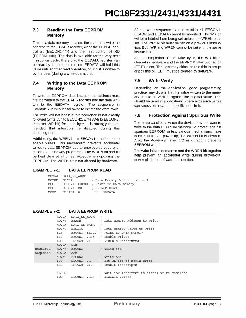
PIC18F2331/2431/4331/4431
7.3 Reading the Data EEPROM Memory
To read a data memory location, the user must write theaddress to the EEADR register, clear the EEPGD con-trol bit (EECON1<7>) and then set control bit RD(EECON1<0>). The data is available for the very nextinstruction cycle; therefore, the EEDATA register canbe read by the next instruction. EEDATA will hold thisvalue until another read operation, or until it is written toby the user (during a write operation).
7.4 Writing to the Data EEPROM Memory
To write an EEPROM data location, the address mustfirst be written to the EEADR register and the data writ-ten to the EEDATA register. The sequence inExample 7-2 must be followed to initiate the write cycle.
The write will not begin if this sequence is not exactlyfollowed (write 55h to EECON2, write AAh to EECON2,then set WR bit) for each byte. It is strongly recom-mended that interrupts be disabled during thiscode segment.
Additionally, the WREN bit in EECON1 must be set toenable writes. This mechanism prevents accidentalwrites to data EEPROM due to unexpected code exe-cution (i.e., runaway programs). The WREN bit shouldbe kept clear at all times, except when updating theEEPROM. The WREN bit is not cleared by hardware.
After a write sequence has been initiated, EECON1,EEADR and EEDATA cannot be modified. The WR bitwill be inhibited from being set unless the WREN bit isset. The WREN bit must be set on a previous instruc-tion. Both WR and WREN cannot be set with the sameinstruction.
At the completion of the write cycle, the WR bit iscleared in hardware and the EEPROM interrupt flag bit(EEIF) is set. The user may either enable this interruptor poll this bit. EEIF must be cleared by software.
7.5 Write Verify
Depending on the application, good programmingpractice may dictate that the value written to the mem-ory should be verified against the original value. Thisshould be used in applications where excessive writescan stress bits near the specification limit.
7.6 Protection Against Spurious Write
There are conditions when the device may not want towrite to the data EEPROM memory. To protect againstspurious EEPROM writes, various mechanisms havebeen built-in. On power-up, the WREN bit is cleared.Also, the Power-up Timer (72 ms duration) preventsEEPROM write.
The write initiate sequence and the WREN bit togetherhelp prevent an accidental write during brown-out,power glitch, or software malfunction.
EXAMPLE 7-1: DATA EEPROM READ
EXAMPLE 7-2: DATA EEPROM WRITE
MOVLW DATA_EE_ADDR ;MOVWF EEADR ; Data Memory Address to readBCF EECON1, EEPGD ; Point to DATA memoryBSF EECON1, RD ; EEPROM ReadMOVF EEDATA, W ; W = EEDATA
MOVLW DATA_EE_ADDR ;MOVWF EEADR ; Data Memory Address to writeMOVLW DATA_EE_DATA ;MOVWF EEDATA ; Data Memory Value to writeBCF EECON1, EEPGD ; Point to DATA memoryBSF EECON1, WREN ; Enable writesBCF INTCON, GIE ; Disable InterruptsMOVLW 55h ;
Required MOVWF EECON2 ; Write 55hSequence MOVLW AAh ;
MOVWF EECON2 ; Write AAhBSF EECON1, WR ; Set WR bit to begin writeBSF INTCON, GIE ; Enable Interrupts
SLEEP ; Wait for interrupt to signal write completeBCF EECON1, WREN ; Disable writes
2003 Microchip Technology Inc. Preliminary DS39616B-page 87

PIC18F2331/2431/4331/4431
7.7 Operation During Code-Protect
Data EEPROM memory has its own code-protect bits inconfiguration words. External Read and Write opera-tions are disabled if either of these mechanisms areenabled.
The microcontroller itself can both read and write to theinternal data EEPROM, regardless of the state of thecode-protect configuration bit. Refer to Section 22.0“Special Features of the CPU” for additionalinformation.
7.8 Using the Data EEPROM
The Data EEPROM is a high-endurance, byteaddressable array that has been optimized for thestorage of frequently changing information (e.g.,program variables or other data that are updatedoften). Frequently changing values will typically beupdated more often than specification D124 or D124A.If this is not the case, an array refresh must beperformed. For this reason, variables that changeinfrequently (such as constants, IDs, calibration, etc.)should be stored in Flash program memory.
A simple data EEPROM refresh routine is shown inExample 7-3.
EXAMPLE 7-3: DATA EEPROM REFRESH ROUTINE
TABLE 7-1: REGISTERS ASSOCIATED WITH DATA EEPROM MEMORY
Note: If data EEPROM is only used to store con-stants and/or data that changes rarely, anarray refresh is likely not required. Seespecification D124 or D124A.
CLRF EEADR ; Start at address 0BCF EECON1, CFGS ; Set for memoryBCF EECON1, EEPGD ; Set for Data EEPROMBCF INTCON, GIE ; Disable interruptsBSF EECON1, WREN ; Enable writes
LOOP ; Loop to refresh arrayBSF EECON1, RD ; Read current addressMOVLW 55h ;MOVWF EECON2 ; Write 55hMOVLW AAh ;MOVWF EECON2 ; Write AAhBSF EECON1, WR ; Set WR bit to begin writeBTFSC EECON1, WR ; Wait for write to completeBRA $-2INCFSZ EEADR, F ; Increment addressBRA Loop ; Not zero, do it again
BCF EECON1, WREN ; Disable writesBSF INTCON, GIE ; Enable interrupts
Name Bit 7 Bit 6 Bit 5 Bit 4 Bit 3 Bit 2 Bit 1 Bit 0Value on:POR, BOR
Value on all other Resets
INTCON GIE/GIEH PEIE/GIEL TMR0IE INTE RBIE TMR0IF INTF RBIF 0000 000x 0000 000u
EEADR EEPROM Address Register 0000 0000 0000 0000
EEDATA EEPROM Data Register 0000 0000 0000 0000
EECON2 EEPROM Control Register2 (not a physical register) — —
EECON1 EEPGD CFGS — FREE WRERR WREN WR RD xx-0 x000 uu-0 u000
IPR2 OSFIP — — EEIP — LVDIP — CCP2IP 1--1 -1-1 1--1 -1-1
PIR2 OSFIF — — EEIF — LVDIF — CCP2IF 0--0 -0-0 0--0 -0-0
PIE2 OSFIE — — EEIE — LVDIE — CCP2IE 0--0 -0-0 0--0 -0-0
Legend: x = unknown, u = unchanged, r = reserved, - = unimplemented, read as ‘0’. Shaded cells are not used during Flash/EEPROM access.
DS39616B-page 88 Preliminary 2003 Microchip Technology Inc.

PIC18F2331/2431/4331/4431
8.0 8 X 8 HARDWARE MULTIPLIER
8.1 Introduction
An 8 x 8 hardware multiplier is included in the ALU ofthe PIC18F2331/2431/4331/4431 devices. By makingthe multiply a hardware operation, it completes in asingle instruction cycle. This is an unsigned multiplythat gives a 16-bit result. The result is stored into the16-bit product register pair (PRODH:PRODL). Themultiplier does not affect any flags in the Statusregister.
Making the 8 x 8 multiplier execute in a single cyclegives the following advantages:
• Higher computational throughput• Reduces code size requirements for multiply
algorithms
The performance increase allows the device to be usedin applications previously reserved for Digital SignalProcessors.
Table 8-1 shows a performance comparison betweenenhanced devices using the single cycle hardware mul-tiply, and performing the same function without thehardware multiply.
TABLE 8-1: PERFORMANCE COMPARISON
8.2 Operation
Example 8-1 shows the sequence to do an 8 x 8unsigned multiply. Only one instruction is requiredwhen one argument of the multiply is already loaded inthe WREG register.
Example 8-2 shows the sequence to do an 8 x 8 signedmultiply. To account for the sign bits of the arguments,each argument’s Most Significant bit (MSb) is testedand the appropriate subtractions are done.
EXAMPLE 8-1: 8 x 8 UNSIGNED MULTIPLY ROUTINE
EXAMPLE 8-2: 8 x 8 SIGNED MULTIPLY ROUTINE
Routine Multiply MethodProgramMemory(Words)
Cycles(Max)
Time
@ 40 MHz @ 10 MHz @ 4 MHz
8 x 8 unsignedWithout hardware multiply 13 69 6.9 µs 27.6 µs 69 µs
Hardware multiply 1 1 100 ns 400 ns 1 µs
8 x 8 signedWithout hardware multiply 33 91 9.1 µs 36.4 µs 91 µs
Hardware multiply 6 6 600 ns 2.4 µs 6 µs
16 x 16 unsignedWithout hardware multiply 21 242 24.2 µs 96.8 µs 242 µs
Hardware multiply 24 24 2.4 µs 9.6 µs 24 µs
16 x 16 signedWithout hardware multiply 52 254 25.4 µs 102.6 µs 254 µs
Hardware multiply 36 36 3.6 µs 14.4 µs 36 µs
MOVF ARG1, W ; MULWF ARG2 ; ARG1 * ARG2 ->
; PRODH:PRODL
MOVF ARG1, W MULWF ARG2 ; ARG1 * ARG2 ->
; PRODH:PRODL BTFSC ARG2, SB ; Test Sign Bit SUBWF PRODH, F ; PRODH = PRODH
; - ARG1 MOVF ARG2, W BTFSC ARG1, SB ; Test Sign Bit SUBWF PRODH, F ; PRODH = PRODH
; - ARG2
2003 Microchip Technology Inc. Preliminary DS39616B-page 89

PIC18F2331/2431/4331/4431
Example 8-3 shows the sequence to do a 16 x 16unsigned multiply. Equation 8-1 shows the algorithmthat is used. The 32-bit result is stored in four registers,RES3:RES0.
EQUATION 8-1: 16 x 16 UNSIGNED MULTIPLICATION ALGORITHM
EXAMPLE 8-3: 16 x 16 UNSIGNED MULTIPLY ROUTINE
Example 8-4 shows the sequence to do a 16 x 16signed multiply. Equation 8-2 shows the algorithmused. The 32-bit result is stored in four registers,RES3:RES0. To account for the sign bits of the argu-ments, each argument pair’s Most Significant bit (MSb)is tested, and the appropriate subtractions are done.
EQUATION 8-2: 16 x 16 SIGNED MULTIPLICATION ALGORITHM
EXAMPLE 8-4: 16 x 16 SIGNED MULTIPLY ROUTINE
MOVFARG1L, W MULWFARG2L ; ARG1L * ARG2L ->
; PRODH:PRODL MOVFFPRODH, RES1 ; MOVFFPRODL, RES0 ;
; MOVFARG1H, W MULWFARG2H ; ARG1H * ARG2H ->
; PRODH:PRODL MOVFFPRODH, RES3 ; MOVFFPRODL, RES2 ;
; MOVFARG1L, W MULWFARG2H ; ARG1L * ARG2H ->
; PRODH:PRODL MOVFPRODL, W ; ADDWFRES1, F ; Add cross MOVFPRODH, W ; products ADDWFCRES2, F ; CLRFWREG ; ADDWFCRES3, F ;
; MOVFARG1H, W ; MULWFARG2L ; ARG1H * ARG2L ->
; PRODH:PRODL MOVFPRODL, W ; ADDWFRES1, F ; Add cross MOVFPRODH, W ; products ADDWFCRES2, F ; CLRFWREG ; ADDWFCRES3, F ;
RES3:RES0 = ARG1H:ARG1L • ARG2H:ARG2L= (ARG1H • ARG2H • 216)+
(ARG1H • ARG2L • 28)+(ARG1L • ARG2H • 28)+(ARG1L • ARG2L)
MOVF ARG1L, W MULWF ARG2L ; ARG1L * ARG2L ->
; PRODH:PRODL MOVFF PRODH, RES1 ; MOVFF PRODL, RES0 ;
; MOVF ARG1H, W MULWF ARG2H ; ARG1H * ARG2H ->
; PRODH:PRODL MOVFF PRODH, RES3 ; MOVFF PRODL, RES2 ;
; MOVF ARG1L, W MULWF ARG2H ; ARG1L * ARG2H ->
; PRODH:PRODL MOVF PRODL, W ; ADDWF RES1, F ; Add cross MOVF PRODH, W ; products ADDWFC RES2, F ; CLRF WREG ; ADDWFC RES3, F ;
; MOVF ARG1H, W ; MULWF ARG2L ; ARG1H * ARG2L ->
; PRODH:PRODL MOVF PRODL, W ; ADDWF RES1, F ; Add cross MOVF PRODH, W ; products ADDWFC RES2, F ; CLRF WREG ; ADDWFC RES3, F ;
; BTFSS ARG2H, 7 ; ARG2H:ARG2L neg? BRA SIGN_ARG1 ; no, check ARG1 MOVF ARG1L, W ; SUBWF RES2 ; MOVF ARG1H, W ; SUBWFB RES3
; SIGN_ARG1
BTFSS ARG1H, 7 ; ARG1H:ARG1L neg? BRA CONT_CODE ; no, done MOVF ARG2L, W ; SUBWF RES2 ; MOVF ARG2H, W ; SUBWFB RES3
; CONT_CODE :
RES3:RES0= ARG1H:ARG1L • ARG2H:ARG2L= (ARG1H • ARG2H • 216)+
(ARG1H • ARG2L • 28)+(ARG1L • ARG2H ² 28)+(ARG1L • ARG2L)+(-1 • ARG2H<7> • ARG1H:ARG1L • 216)+(-1 • ARG1H<7> • ARG2H:ARG2L • 216)
DS39616B-page 90 Preliminary 2003 Microchip Technology Inc.
PIC18F2331/2431/4331/4431
9.0 INTERRUPTS
The PIC18F2331/2431/4331/4431 devices havemultiple interrupt sources and an interrupt priorityfeature that allows each interrupt source to be assigneda high priority level or a low priority level. The highpriority interrupt vector is at 000008h and the lowpriority interrupt vector is at 000018h. High priorityinterrupt events will interrupt any low priority interruptsthat may be in progress.
There are ten registers which are used to controlinterrupt operation. These registers are:
• RCON• INTCON
• INTCON2• INTCON3• PIR1, PIR2, PIR3
• PIE1, PIE2, PIE3• IPR1, IPR2, IPR3
It is recommended that the Microchip header files sup-plied with MPLAB® IDE be used for the symbolic bitnames in these registers. This allows the assembler/compiler to automatically take care of the placement ofthese bits within the specified register.
In general, each interrupt source has three bits to con-trol its operation. The functions of these bits are:
• Flag bit to indicate that an interrupt event occurred
• Enable bit that allows program execution to branch to the interrupt vector address when the flag bit is set
• Priority bit to select high priority or low priority (most interrupt sources have priority bits)
The interrupt priority feature is enabled by setting theIPEN bit (RCON<7>). When interrupt priority isenabled, there are two bits which enable interruptsglobally. Setting the GIEH bit (INTCON<7>) enables allinterrupts that have the priority bit set (high priority).Setting the GIEL bit (INTCON<6>) enables allinterrupts that have the priority bit cleared (low priority).When the interrupt flag, enable bit and appropriateglobal interrupt enable bit are set, the interrupt willvector immediately to address 000008h or 000018h,depending on the priority bit setting. Individualinterrupts can be disabled through their correspondingenable bits.
When the IPEN bit is cleared (default state), the inter-rupt priority feature is disabled and interrupts are com-patible with PICmicro® mid-range devices. InCompatibility mode, the interrupt priority bits for eachsource have no effect. INTCON<6> is the PEIE bit,which enables/disables all peripheral interrupt sources.INTCON<7> is the GIE bit, which enables/disables allinterrupt sources. All interrupts branch to address000008h in Compatibility mode.
When an interrupt is responded to, the Global InterruptEnable bit is cleared to disable further interrupts. If theIPEN bit is cleared, this is the GIE bit. If interrupt prioritylevels are used, this will be either the GIEH or GIEL bit.High priority interrupt sources can interrupt a lowpriority interrupt. Low priority interrupts are notprocessed while high priority interrupts are in progress.
The return address is pushed onto the stack and thePC is loaded with the interrupt vector address(000008h or 000018h). Once in the interrupt serviceroutine, the source(s) of the interrupt can bedetermined by polling the interrupt flag bits. Theinterrupt flag bits must be cleared in software before re-enabling interrupts to avoid recursive interrupts.
The “return from interrupt” instruction, RETFIE, exitsthe interrupt routine and sets the GIE bit (GIEH or GIELif priority levels are used), which re-enables interrupts.
For external interrupt events, such as the INT pins orthe PORTB input change interrupt, the interrupt latencywill be three to four instruction cycles. The exactlatency is the same for one or two-cycle instructions.Individual interrupt flag bits are set, regardless of thestatus of their corresponding enable bit or the GIE bit.
Note: Do not use the MOVFF instruction to modifyany of the interrupt control registers whileany interrupt is enabled. Doing so maycause erratic microcontroller behavior.
2003 Microchip Technology Inc. Preliminary DS39616B-page 91

PIC18F2331/2431/4331/4431
FIGURE 9-1: INTERRUPT LOGIC
TMR0IE
GIEH/GIE
GIEL/PEIE
Wake-up if in
Interrupt to CPUVector to Location0008h
INT2IFINT2IEINT2IP
INT1IFINT1IEINT1IP
TMR0IFTMR0IETMR0IP
INT0IFINT0IE
RBIFRBIERBIP
IPEN
TMR0IF
TMR0IP
INT1IFINT1IEINT1IPINT2IFINT2IEINT2IP
RBIFRBIERBIP
INT0IFINT0IE
GIEL\PEIE
Interrupt to CPUVector to Location
IPEN
IPE
0018h
PSPIFPSPIEPSPIP
PSPIFPSPIEPSPIP
ADIFADIEADIP
RCIFRCIERCIP
Additional Peripheral Interrupts
ADIFADIEADIP
High Priority Interrupt Generation
Low Priority Interrupt Generation
RCIFRCIERCIP
Additional Peripheral Interrupts
Power-Managed mode
DS39616B-page 92 Preliminary 2003 Microchip Technology Inc.

PIC18F2331/2431/4331/4431
9.1 INTCON Registers
The INTCON Registers are readable and writableregisters, which contain various enable, priority andflag bits.
REGISTER 9-1: INTCON REGISTER
Note: Interrupt flag bits are set when an interruptcondition occurs, regardless of the state ofits corresponding enable bit or the globalenable bit. User software should ensurethe appropriate interrupt flag bits are clearprior to enabling an interrupt. This featureallows for software polling.
R/W-0 R/W-0 R/W-0 R/W-0 R/W-0 R/W-0 R/W-0 R/W-x
GIE/GIEH PEIE/GIEL TMR0IE INT0IE RBIE TMR0IF INT0IF RBIF
bit 7 bit 0
bit 7 GIE/GIEH: Global Interrupt Enable bit
When IPEN = 0:1 = Enables all unmasked interrupts0 = Disables all interrupts When IPEN = 1:
1 = Enables all high priority interrupts 0 = Disables all high priority interrupts
bit 6 PEIE/GIEL: Peripheral Interrupt Enable bitWhen IPEN = 0:
1 = Enables all unmasked peripheral interrupts 0 = Disables all peripheral interrupts When IPEN = 1:1 = Enables all low priority peripheral interrupts 0 = Disables all low priority peripheral interrupts
bit 5 TMR0IE: TMR0 Overflow Interrupt Enable bit 1 = Enables the TMR0 overflow interrupt 0 = Disables the TMR0 overflow interrupt
bit 4 INT0IE: INT0 External Interrupt Enable bit
1 = Enables the INT0 external interrupt 0 = Disables the INT0 external interrupt
bit 3 RBIE: RB Port Change Interrupt Enable bit 1 = Enables the RB port change interrupt for RB7:RB4 pins 0 = Disables the RB port change interrupt for RB7:RB4 pins
bit 2 TMR0IF: TMR0 Overflow Interrupt Flag bit 1 = TMR0 register has overflowed (must be cleared in software) 0 = TMR0 register did not overflow
bit 1 INT0IF: INT0 External Interrupt Flag bit
1 = The INT0 external interrupt occurred (must be cleared in software) 0 = The INT0 external interrupt did not occur
bit 0 RBIF: RB Port Change Interrupt Flag bit 1 = At least one of the RB7:RB4 pins changed state (must be cleared in software) 0 = None of the RB7:RB4 pins have changed state
Note: A mismatch condition will continue to set this bit. Reading PORTB will end the mismatch condition and allow the bit to be cleared.
Legend:
R = Readable bit W = Writable bit U = Unimplemented bit, read as ‘0’
- n = Value at POR ‘1’ = Bit is set ‘0’ = Bit is cleared x = Bit is unknown
2003 Microchip Technology Inc. Preliminary DS39616B-page 93

PIC18F2331/2431/4331/4431
REGISTER 9-2: INTCON2 REGISTER
R/W-1 R/W-1 R/W-1 R/W-1 U-0 R/W-1 U-0 R/W-1
RBPU INTEDG0 INTEDG1 INTEDG2 — TMR0IP — RBIP
bit 7 bit 0
bit 7 RBPU: PORTB Pull-up Enable bit 1 = All PORTB pull-ups are disabled 0 = PORTB pull-ups are enabled by individual port latch values
bit 6 INTEDG0: External Interrupt0 Edge Select bit
1 = Interrupt on rising edge 0 = Interrupt on falling edge
bit 5 INTEDG1: External Interrupt1 Edge Select bit 1 = Interrupt on rising edge 0 = Interrupt on falling edge
bit 4 INTEDG2: External Interrupt2 Edge Select bit 1 = Interrupt on rising edge 0 = Interrupt on falling edge
bit 3 Unimplemented: Read as ‘0’
bit 2 TMR0IP: TMR0 Overflow Interrupt Priority bit 1 = High priority 0 = Low priority
bit 1 Unimplemented: Read as ‘0’
bit 0 RBIP: RB Port Change Interrupt Priority bit
1 = High priority 0 = Low priority
Legend:
R = Readable bit W = Writable bit U = Unimplemented bit, read as ‘0’
- n = Value at POR ‘1’ = Bit is set ‘0’ = Bit is cleared x = Bit is unknown
Note: Interrupt flag bits are set when an interrupt condition occurs, regardless of the stateof its corresponding enable bit or the global enable bit. User software should ensurethe appropriate interrupt flag bits are clear prior to enabling an interrupt. This featureallows for software polling.
DS39616B-page 94 Preliminary 2003 Microchip Technology Inc.

PIC18F2331/2431/4331/4431
REGISTER 9-3: INTCON3 REGISTER
R/W-1 R/W-1 U-0 R/W-0 R/W-0 U-0 R/W-0 R/W-0
INT2IP INT1IP — INT2IE INT1IE — INT2IF INT1IF
bit 7 bit 0
bit 7 INT2IP: INT2 External Interrupt Priority bit1 = High priority 0 = Low priority
bit 6 INT1IP: INT1 External Interrupt Priority bit
1 = High priority 0 = Low priority
bit 5 Unimplemented: Read as ‘0’
bit 4 INT2IE: INT2 External Interrupt Enable bit1 = Enables the INT2 external interrupt 0 = Disables the INT2 external interrupt
bit 3 INT1IE: INT1 External Interrupt Enable bit
1 = Enables the INT1 external interrupt 0 = Disables the INT1 external interrupt
bit 2 Unimplemented: Read as ‘0’
bit 1 INT2IF: INT2 External Interrupt Flag bit1 = The INT2 external interrupt occurred (must be cleared in software) 0 = The INT2 external interrupt did not occur
bit 0 INT1IF: INT1 External Interrupt Flag bit
1 = The INT1 external interrupt occurred (must be cleared in software) 0 = The INT1 external interrupt did not occur
Legend:
R = Readable bit W = Writable bit U = Unimplemented bit, read as ‘0’
- n = Value at POR ‘1’ = Bit is set ‘0’ = Bit is cleared x = Bit is unknown
Note: Interrupt flag bits are set when an interrupt condition occurs, regardless of the stateof its corresponding enable bit or the global enable bit. User software should ensurethe appropriate interrupt flag bits are clear prior to enabling an interrupt. This featureallows for software polling.
2003 Microchip Technology Inc. Preliminary DS39616B-page 95

PIC18F2331/2431/4331/4431
9.2 PIR Registers
The PIR registers contain the individual flag bits for theperipheral interrupts. Due to the number of peripheralinterrupt sources, there are two Peripheral InterruptFlag Registers (PIR1, PIR2).
REGISTER 9-4: PIR1: PERIPHERAL INTERRUPT REQUEST (FLAG) REGISTER 1
Note 1: Interrupt flag bits are set when an interruptcondition occurs, regardless of the state ofits corresponding enable bit or the globalenable bit, GIE (INTCON<7>).
2: User software should ensure the appropri-ate interrupt flag bits are cleared prior toenabling an interrupt, and after servicingthat interrupt.
U-0 R/W-0 R-0 R-0 R/W-0 R/W-0 R/W-0 R/W-0
— ADIF RCIF TXIF SSPIF CCP1IF TMR2IF TMR1IF
bit 7 bit 0
bit 7 Unimplemented: Read as ‘0’.
bit 6 ADIF: A/D Converter Interrupt Flag bit 1 = An A/D conversion completed (must be cleared in software) 0 = The A/D conversion is not complete
bit 5 RCIF: USART Receive Interrupt Flag bit
1 = The USART receive buffer, RCREG, is full (cleared when RCREG is read) 0 = The USART receive buffer is empty
bit 4 TXIF: USART Transmit Interrupt Flag bit 1 = The USART transmit buffer, TXREG, is empty (cleared when TXREG is written) 0 = The USART transmit buffer is full
bit 3 SSPIF: Synchronous Serial Port Interrupt Flag bit 1 = The transmission/reception is complete (must be cleared in software)0 = Waiting to transmit/receive
bit 2 CCP1IF: CCP1 Interrupt Flag bit Capture mode: 1 = A TMR1 register capture occurred (must be cleared in software) 0 = No TMR1 register capture occurred Compare mode:
1 = A TMR1 register compare match occurred (must be cleared in software) 0 = No TMR1 register compare match occurredPWM mode: Unused in this mode
bit 1 TMR2IF: TMR2 to PR2 Match Interrupt Flag bit
1 = TMR2 to PR2 match occurred (must be cleared in software) 0 = No TMR2 to PR2 match occurred
bit 0 TMR1IF: TMR1 Overflow Interrupt Flag bit 1 = TMR1 register overflowed (must be cleared in software)0 = TMR1 register did not overflow
Note 1: This bit is reserved on PIC18F2X31 devices; always maintain this bit clear.
Legend:
R = Readable bit W = Writable bit U = Unimplemented bit, read as ‘0’
- n = Value at POR ‘1’ = Bit is set ‘0’ = Bit is cleared x = Bit is unknown
DS39616B-page 96 Preliminary 2003 Microchip Technology Inc.

PIC18F2331/2431/4331/4431
REGISTER 9-5: PIR2: PERIPHERAL INTERRUPT REQUEST (FLAG) REGISTER 2 R/W-0 U-0 U-0 R/W-0 U-0 R/W-0 U-0 R/W-0
OSFIF — — EEIF — LVDIF — CCP2IF
bit 7 bit 0
bit 7 OSFIF: Oscillator Fail Interrupt Flag bit
1 = System Oscillator failed, clock input has changed to INTOSC (must be cleared in software)0 = System clock operating
bit 6-5 Unimplemented: Read as ‘0’
bit 4 EEIF: EEPROM or Flash Write Operation Interrupt Flag bit1 = The write operation is complete (must be cleared in software)0 = The write operation is not complete or has not been started
bit 3 Unimplemented: Read as ‘0’
bit 2 LVDIF: Low-Voltage Detect Interrupt Flag bit1 = The supply voltage has fallen below the specified LVD voltage (must be cleared in
software)0 = The supply voltage is greater than the specified LVD voltage
bit 1 Unimplemented: Read as ‘0’
bit 0 CCP2IF: CCP2 Interrupt Flag bitCapture mode:1 = A TMR1 register capture occurred (must be cleared in software)0 = No TMR1 register capture occurredCompare mode:1 = A TMR1 register compare match occurred (must be cleared in software)0 = No TMR1 register compare match occurredPWM mode:Not used in PWM mode
Legend:
R = Readable bit W = Writable bit U = Unimplemented bit, read as ‘0’
- n = Value at POR ‘1’ = Bit is set ‘0’ = Bit is cleared x = Bit is unknown
2003 Microchip Technology Inc. Preliminary DS39616B-page 97

PIC18F2331/2431/4331/4431
REGISTER 9-6: PIR3: PERIPHERAL INTERRUPT FLAG REGISTER 3 U-0 U-0 U-0 R/W-0 R/W-0 R/W-0 R/W-0 R/W-0— — — PTIF IC3DRIF IC2QEIF IC1IF TMR5IF
bit 7 bit 0
bit 7-5 Unimplemented: Read as ‘0’
bit 4 PTIF: PWM Time Base Interrupt bit
1 = PWM Time Base matched the value in PTPER register. Interrupt is issued according to thepostscaler settings. PTIF must be cleared in software.
0 = PWM Time Base has not matched the value in PTPER register.
bit 3 IC3DRIF: IC3 Interrupt Flag/Direction Change Interrupt Flag bitIC3 Enabled (CAP3CON<3:0>)1 = TMR5 value was captured by the active edge on CAP3 input (must be cleared in software).0 = TMR5 capture has not occurred.QEI Enabled (QEIM<2:0>)1 = Direction of rotation has changed (must be cleared in software).0 = Direction of rotation has not changed.
bit 2 IC2QEIF: IC2 Interrupt Flag/QEI Interrupt Flag bitIC2 Enabled (CAP2CON<3:0>)1 = TMR5 value was captured by the active edge on CAP2 input (must be cleared in software).0 = TMR5 capture has not occurred.QEI Enabled (QEIM<2:0>)1 = The QEI position counter has reached the MAXCNT value or the index pulse, INDX, has
been detected. Depends on the QEI operating mode enabled. Must be cleared in software.0 = The QEI position counter has not reached the MAXCNT value or the index pulse has not
been detected.
bit 1 IC1IF: IC1 Interrupt Flag bitIC1 Enabled (CAP1CON<3:0>)1 = TMR5 value was captured by the active edge on CAP1 input (must be cleared in software).0 = TMR5 capture has not occurred.QEI Enabled (QEIM<2:0>) and Velocity Measurement mode enabled
(VELM = 0 in QEICON Register)1 = Timer5 value was captured by the active velocity edge (based on PHA or PHB input).
CAP1REN bit must be set in CAP1CON register. IC1IF must be cleared in software.0 = Timer5 value was not captured by the active velocity edge.
bit 0 TMR5IF: Timer5 Interrupt Flag bit
1 = Timer5 time base matched the PR5 value (must be cleared in software).0 = Timer5 time base did not match the PR5 value.
Legend:
R = Readable bit W = Writable bit U = Unimplemented bit, read as ‘0’
-n = Value at POR ‘1’ = bit is set ‘0’ = bit is cleared x = bit is unknown
DS39616B-page 98 Preliminary 2003 Microchip Technology Inc.
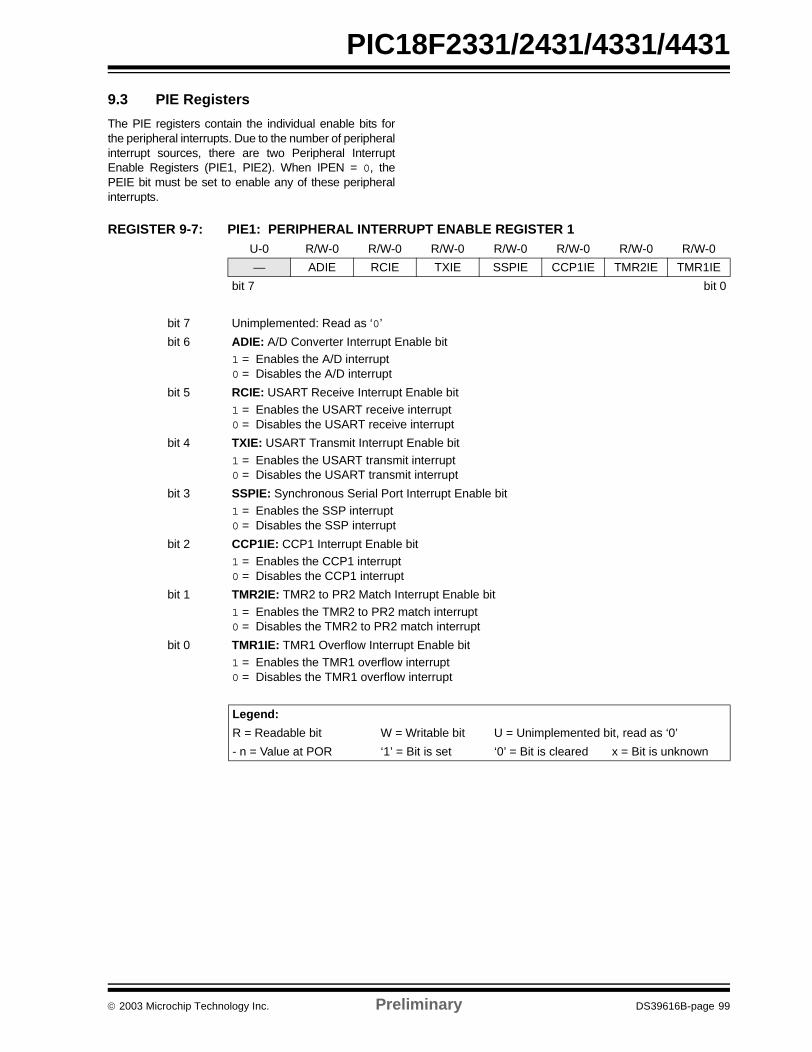
PIC18F2331/2431/4331/4431
9.3 PIE Registers
The PIE registers contain the individual enable bits forthe peripheral interrupts. Due to the number of peripheralinterrupt sources, there are two Peripheral InterruptEnable Registers (PIE1, PIE2). When IPEN = 0, thePEIE bit must be set to enable any of these peripheralinterrupts.
REGISTER 9-7: PIE1: PERIPHERAL INTERRUPT ENABLE REGISTER 1 U-0 R/W-0 R/W-0 R/W-0 R/W-0 R/W-0 R/W-0 R/W-0
— ADIE RCIE TXIE SSPIE CCP1IE TMR2IE TMR1IE
bit 7 bit 0
bit 7 Unimplemented: Read as ‘0’
bit 6 ADIE: A/D Converter Interrupt Enable bit1 = Enables the A/D interrupt0 = Disables the A/D interrupt
bit 5 RCIE: USART Receive Interrupt Enable bit1 = Enables the USART receive interrupt0 = Disables the USART receive interrupt
bit 4 TXIE: USART Transmit Interrupt Enable bit
1 = Enables the USART transmit interrupt0 = Disables the USART transmit interrupt
bit 3 SSPIE: Synchronous Serial Port Interrupt Enable bit1 = Enables the SSP interrupt0 = Disables the SSP interrupt
bit 2 CCP1IE: CCP1 Interrupt Enable bit1 = Enables the CCP1 interrupt0 = Disables the CCP1 interrupt
bit 1 TMR2IE: TMR2 to PR2 Match Interrupt Enable bit
1 = Enables the TMR2 to PR2 match interrupt0 = Disables the TMR2 to PR2 match interrupt
bit 0 TMR1IE: TMR1 Overflow Interrupt Enable bit1 = Enables the TMR1 overflow interrupt0 = Disables the TMR1 overflow interrupt
Legend:
R = Readable bit W = Writable bit U = Unimplemented bit, read as ‘0’
- n = Value at POR ‘1’ = Bit is set ‘0’ = Bit is cleared x = Bit is unknown
2003 Microchip Technology Inc. Preliminary DS39616B-page 99

PIC18F2331/2431/4331/4431
REGISTER 9-8: PIE2: PERIPHERAL INTERRUPT ENABLE REGISTER 2 R/W-0 U-0 U-0 R/W-0 U-0 R/W-0 U-0 R/W-0
OSFIE — — EEIE — LVDIE — CCP2IE
bit 7 bit 0
bit 7 OSFIE: Oscillator Fail Interrupt Enable bit1 = Enabled0 = Disabled
bit 6-5 Unimplemented: Read as ‘0’
bit 4 EEIE: Interrupt Enable bit1 = Enabled0 = Disabled
bit 3 Unimplemented: Read as ‘0’
bit 2 LVDIE: Low-Voltage Detect Interrupt Enable bit
1 = Enabled0 = Disabled
bit 1 Unimplemented: Read as ‘0’
bit 0 CCP2IE: CCP2 Interrupt Enable bit1 = Enabled0 = Disabled
Legend:
R = Readable bit W = Writable bit U = Unimplemented bit, read as ‘0’
- n = Value at POR ‘1’ = Bit is set ‘0’ = Bit is cleared x = Bit is unknown
DS39616B-page 100 Preliminary 2003 Microchip Technology Inc.

PIC18F2331/2431/4331/4431
REGISTER 9-9: PIE3: PERIPHERAL INTERRUPT ENABLE REGISTER 3 U-0 U-0 U-0 R/W-0 R/W-0 R/W-0 R/W-0 R/W-0— — — PTIE IC3DRIE IC2QEIE IC1IE TMR5IE
bit 7 bit 0
bit 7-5 Unimplemented: Read as ‘0’
bit 4 PTIE: PWM Time Base Interrupt Enable bit
1 = PTIF enabled0 = PTIF disabled
bit 3 IC3DRIE: IC3 Interrupt Enable/Direction Change Interrupt Enable bitIC3 Enabled (CAP3CON<3:0>)1 = IC3 interrupt enabled0 = IC3 interrupt disabledQEI Enabled (QEIM<2:0>)1 = Change-of-direction interrupt enabled0 = Change-of-direction interrupt disabled
bit 2 IC2QEIE: IC2 Interrupt Flag/QEI Interrupt Flag Enable bit
IC2 Enabled (CAP2CON<3:0>)1 = IC2 interrupt enabled)0 = IC2 interrupt disabledQEI Enabled (QEIM<2:0>)1 = QEI interrupt enabled0 = QEI interrupt disabled
bit 1 IC1IE: IC1 Interrupt Enable bit1 = IC1 interrupt enabled0 = IC1 interrupt disabled
bit 0 TMR5IE: Timer5 Interrupt Enable bit
1 = Timer5 interrupt enabled0 = Timer5 interrupt disabled
Legend:
R = Readable bit W = Writable bit U = Unimplemented bit, read as ‘0’
-n = Value at POR ‘1’ = bit is set ‘0’ = bit is cleared x = bit is unknown
2003 Microchip Technology Inc. Preliminary DS39616B-page 101

PIC18F2331/2431/4331/4431
9.4 IPR Registers
The IPR registers contain the individual priority bits forthe peripheral interrupts. Due to the number ofperipheral interrupt sources, there are two peripheralinterrupt priority registers (IPR1, IPR2). Using thepriority bits requires that the Interrupt Priority Enable(IPEN) bit be set.
REGISTER 9-10: IPR1: PERIPHERAL INTERRUPT PRIORITY REGISTER 1 U-0 R/W-1 R/W-1 R/W-1 R/W-1 R/W-1 R/W-1 R/W-1
— ADIP RCIP TXIP SSPIP CCP1IP TMR2IP TMR1IP
bit 7 bit 0
bit 7 Unimplemented: Read as ‘0’
bit 6 ADIP: A/D Converter Interrupt Priority bit1 = High priority0 = Low priority
bit 5 RCIP: USART Receive Interrupt Priority bit
1 = High priority0 = Low priority
bit 4 TXIP: USART Transmit Interrupt Priority bit1 = High priority0 = Low priority
bit 3 SSPIP: Synchronous Serial Port Interrupt Priority bit1 = High priority0 = Low priority
bit 2 CCP1IP: CCP1 Interrupt Priority bit
1 = High priority0 = Low priority
bit 1 TMR2IP: TMR2 to PR2 Match Interrupt Priority bit1 = High priority0 = Low priority
bit 0 TMR1IP: TMR1 Overflow Interrupt Priority bit1 = High priority0 = Low priority
Legend:
R = Readable bit W = Writable bit U = Unimplemented bit, read as ‘0’
- n = Value at POR ‘1’ = Bit is set ‘0’ = Bit is cleared x = Bit is unknown
DS39616B-page 102 Preliminary 2003 Microchip Technology Inc.

PIC18F2331/2431/4331/4431
REGISTER 9-11: IPR2: PERIPHERAL INTERRUPT PRIORITY REGISTER 2 R/W-1 U-0 U-0 R/W-1 U-0 R/W-1 U-0 R/W-1
OSFIP — — EEIP — LVDIP — CCP2IP
bit 7 bit 0
bit 7 OSFIP: Oscillator Fail Interrupt Priority bit1 = High priority0 = Low priority
bit 6-5 Unimplemented: Read as ‘0’
bit 4 EEIP: Interrupt Priority bit1 = High priority0 = Low priority
bit 3 Unimplemented: Read as ‘0’
bit 2 LVDIP: Low-Voltage Detect Interrupt Priority bit
1 = High priority0 = Low priority
bit 1 Unimplemented: Read as ‘0’
bit 0 CCP2IP: CCP2 Interrupt Priority bit1 = High priority0 = Low priority
Legend:
R = Readable bit W = Writable bit U = Unimplemented bit, read as ‘0’
- n = Value at POR ‘1’ = Bit is set ‘0’ = Bit is cleared x = Bit is unknown
2003 Microchip Technology Inc. Preliminary DS39616B-page 103

PIC18F2331/2431/4331/4431
REGISTER 9-12: IPR3: PERIPHERAL INTERRUPT PRIORITY REGISTER 3 U-0 U-0 U-0 R/W-1 R/W-1 R/W-1 R/W-1 R/W-1
— — PTIP IC3DRIP IC2QEIP IC1IP TMR5IP
bit 7 bit 0
bit 7-5 Unimplemented: Read as ‘0’
bit 4 PTIP: PWM Time Base Interrupt Priority bit
1 = High Priority0 = Low Priority
bit 3 IC3DRIP: IC3 Interrupt Priority/Direction Change Interrupt Priority bitIC3 Enabled (CAP3CON<3:0>)1 = IC3 Interrupt High Priority0 = IC3 Interrupt Low PriorityQEI Enabled (QEIM<2:0>)1 = Change of Direction Interrupt High Priority0 = Change of Direction interrupt Low Priority
bit 2 IC2QEIP: IC2 Interrupt Priority/QEI Interrupt Priority bit
IC2 Enabled (CAP2CON<3:0>)1 = IC2 Interrupt High Priority0 = IC2 Interrupt Low PriorityQEI Enabled (QEIM<2:0>)1 = High Priority0 = Low Priority
bit 1 IC1IP: IC1 Interrupt Priority bit1 = High Priority0 = Low Priority
bit 0 TMR5IP: Timer5 Interrupt Priority bit
1 = High Priority0 = Low Priority
Legend:
R = Readable bit W = Writable bit U = Unimplemented bit, read as ‘0’
-n = Value at POR ‘1’ = bit is set ‘0’ = bit is cleared x = bit is unknown
DS39616B-page 104 Preliminary 2003 Microchip Technology Inc.

PIC18F2331/2431/4331/4431
9.5 RCON Register
The RCON register contains bits used to determine thecause of the last Reset or wake-up from power-managed mode. RCON also contains the bit thatenables interrupt priorities (IPEN).
REGISTER 9-13: RCON REGISTER R/W-0 U-0 U-0 R/W-1 R-1 R-1 R/W-0 R/W-0
IPEN — — RI TO PD POR BOR
bit 7 bit 0
bit 7 IPEN: Interrupt Priority Enable bit 1 = Enable priority levels on interrupts0 = Disable priority levels on interrupts (PIC16CXXX Compatibility mode)
bit 6-5 Unimplemented: Read as ‘0’
bit 4 RI: RESET Instruction Flag bit For details of bit operation, see Register 5-3
bit 3 TO: Watchdog Time-out Flag bit For details of bit operation, see Register 5-3
bit 2 PD: Power-down Detection Flag bit For details of bit operation, see Register 5-3
bit 1 POR: Power-on Reset Status bitFor details of bit operation, see Register 5-3
bit 0 BOR: Brown-out Reset Status bit For details of bit operation, see Register 5-3
Legend:
R = Readable bit W = Writable bit U = Unimplemented bit, read as ‘0’
- n = Value at POR ‘1’ = Bit is set ‘0’ = Bit is cleared x = Bit is unknown
2003 Microchip Technology Inc. Preliminary DS39616B-page 105

PIC18F2331/2431/4331/4431
9.6 INTn Pin Interrupts
External interrupts on the RC3/INT0, RC4/INT1 andRC5/INT2 pins are edge triggered: either rising, if thecorresponding INTEDGx bit is set in the INTCON2register, or falling, if the INTEDGx bit is clear. When avalid edge appears on the RC3/INT0 pin, thecorresponding flag bit INTxF is set. This interrupt canbe disabled by clearing the corresponding enable bitINTxE. Flag bit INTxF must be cleared in software inthe interrupt service routine before re-enabling theinterrupt. All external interrupts (INT0, INT1 and INT2)can wake-up the processor from the power-managedmodes, if bit INTxE was set prior to going into power-managed modes. If the global interrupt enable bit GIEis set, the processor will branch to the interrupt vectorfollowing wake-up.
Interrupt priority for INT1 and INT2 is determined by thevalue contained in the interrupt priority bits, INT1IP(INTCON3<6>) and INT2IP (INTCON3<7>). There isno priority bit associated with INT0. It is always a highpriority interrupt source.
9.7 TMR0 Interrupt
In 8-bit mode (which is the default), an overflow(FFh → 00h) in the TMR0 register will set flag bitTMR0IF. In 16-bit mode, an overflow (FFFFh → 0000h)in the TMR0H:TMR0L registers will set flag bit TMR0IF.The interrupt can be enabled/disabled by setting/clear-ing enable bit TMR0IE (INTCON<5>). Interrupt priorityfor Timer0 is determined by the value contained in theinterrupt priority bit TMR0IP (INTCON2<2>). SeeSection 11.0 “Timer0 Module” for further details.
9.8 PORTB Interrupt-on-Change
An input change on PORTB<7:4> sets flag bit RBIF(INTCON<0>). The interrupt can be enabled/disabledby setting/clearing enable bit, RBIE (INTCON<3>).Interrupt priority for PORTB interrupt-on-change isdetermined by the value contained in the interruptpriority bit, RBIP (INTCON2<0>).
9.9 Context Saving During Interrupts
During interrupts, the return PC address is saved onthe stack. Additionally, the WREG, Status and BSRregisters are saved on the fast return stack. If a fastreturn from interrupt is not used (See Section 5.3“Fast Register Stack”), the user may need to save theWREG, Status and BSR registers on entry to theinterrupt service routine. Depending on the user’sapplication, other registers may also need to be saved.Example 9-1 saves and restores the WREG, Statusand BSR registers during an interrupt service routine.
EXAMPLE 9-1: SAVING STATUS, WREG AND BSR REGISTERS IN RAM MOVWF W_TEMP ; W_TEMP is in virtual bankMOVFF STATUS,STATUS_TEMP ; STATUS_TEMP located anywhereMOVFF BSR,BSR_TEMP ; BSR_TMEP located anywhere;; USER ISR CODE;MOVFF BSR_TEMP,BSR ; Restore BSRMOVF W_TEMP, W ; Restore WREGMOVFF STATUS_TEMP, STATUS ; Restore STATUS
DS39616B-page 106 Preliminary 2003 Microchip Technology Inc.

PIC18F2331/2431/4331/4431
10.0 I/O PORTS
Depending on the device selected and featuresenabled, there are up to five ports available. Some pinsof the I/O ports are multiplexed with an alternatefunction from the peripheral features on the device. Ingeneral, when a peripheral is enabled, that pin may notbe used as a general purpose I/O pin.
Each port has three registers for its operation. Theseregisters are:
• TRIS register (data direction register)• PORT register (reads the levels on the pins of the
device)• LAT register (output latch)
The data latch (LAT register) is useful for read-modify-write operations on the value that the I/O pins aredriving.
A simplified model of a generic I/O port without theinterfaces to other peripherals is shown in Figure 10-1.
FIGURE 10-1: GENERIC I/O PORT OPERATION
10.1 PORTA, TRISA and LATA Registers
PORTA is a 8-bit wide, bidirectional port. The corre-sponding data direction register is TRISA. Setting aTRISA bit (= 1) will make the corresponding PORTA pinan input (i.e., put the corresponding output driver in aHigh-Impedance mode). Clearing a TRISA bit (= 0) willmake the corresponding PORTA pin an output (i.e., putthe contents of the output latch on the selected pin).
Reading the PORTA register reads the status of thepins, whereas writing to it, will write to the port latch.
The Data Latch register (LATA) is also memory mapped.Read-modify-write operations on the LATA register readand write the latched output value for PORTA.
The RA<2:4> pins are multiplexed with three inputcapture pins and Quadrature Encoder Interface pins.Pins RA6 and RA7 are multiplexed with the mainoscillator pins; they are enabled as oscillator or I/O pinsby the selection of the main oscillator in ConfigurationRegister 1H (see Section 22.1 “Configuration Bits”for details). When they are not used as port pins, RA6and RA7 and their associated TRIS and LAT bits areread as ‘0’.
The other PORTA pins are multiplexed with analoginputs, the analog VREF+ and VREF- inputs and the com-parator voltage reference output. The operation of pinsRA3:RA0 and RA5 as A/D converter inputs is selectedby clearing/setting the control bits in the ANSEL0 andANSEL1 registers.
The TRISA register controls the direction of the RApins, even when they are being used as analog inputs.The user must ensure the bits in the TRISA register aremaintained set when using them as analog inputs.
EXAMPLE 10-1: INITIALIZING PORTA
DataBus
WR LAT
WR TRIS
RD PORT
Data Latch
TRIS Latch
RD TRIS
InputBuffer
I/O pin(1)
QD
CK
QD
CK
EN
Q D
EN
RD LAT
or PORT
Note 1: I/O pins have diode protection to VDD and VSS.
Note 1: On a Power-on Reset, RA5:RA0 are con-figured as analog inputs and read as ‘0’.
2: RA5 I/F is available only on 40-pindevices (PIC18F4X31).
CLRF PORTA ; Initialize PORTA by; clearing output; data latches
CLRF LATA ; Alternate method; to clear output; data latches
MOVLW 0x3F ; Configure A/D MOVWF ANSEL0 ; for digital inputsMOVLW 0xCF ; Value used to
; initialize data ; direction
MOVWF TRISA ; Set RA<3:0> as inputs; RA<5:4> as outputs
2003 Microchip Technology Inc. Preliminary DS39616B-page 107

PIC18F2331/2431/4331/4431
FIGURE 10-2: BLOCK DIAGRAM OF RA0 FIGURE 10-3: BLOCK DIAGRAM OF RA1
FIGURE 10-4: BLOCK DIAGRAM OF RA3:RA2 PINS
DataBus
QD
QCK
QD
QCK
Q D
EN
P
N
WR LATA
WR TRISA
Data Latch
TRIS Latch
RD TRISA
RD PORTA
VSS
VDD
I/O Pin
AnalogInputMode
TTLInputBuffer
To A/D Converter
RD LATA
orPORTA
Data Bus
WR LATA
WR TRISA
Data Latch
TRIS Latch
RD TRISA
QD
QCK
Q D
EN
QD
QCK
P
N
VDD
VSS
RD PORTA
RA1orPORTA
RD LATA
AnalogInputMode
To A/D Converter
TTL
Data Bus
WR LATA
WR TRISA
Data Latch
TRIS Latch
RD TRISA
QD
QCK
Q D
EN
QD
QCK
P
N
VDD
VSS
RD PORTA
I/O Pin
orPORTA
RD LATA
AnalogInputMode
To A/D Converter
TTLSchmittTriggerInputBuffer
To CAP1/INDX or CAP2/QEA
DS39616B-page 108 Preliminary 2003 Microchip Technology Inc.

PIC18F2331/2431/4331/4431
FIGURE 10-5: BLOCK DIAGRAM OF RA4
DataBus
QD
QCK
QD
QCK
Q D
EN
WR LATA
WR TRISA
Data Latch
TRIS Latch
RD TRISA
RD PORTA
RA4(1)
Note 1: Open-drain usually available on RA4 has been removed for this device.
AnalogInputMode
TTLInputBuffer
To A/D Converter
RD LATA
orPORTA
To CAP3/QEB
P
N
VSS
VDD
SchmittTriggerInputBuffer
2003 Microchip Technology Inc. Preliminary DS39616B-page 109

PIC18F2331/2431/4331/4431
FIGURE 10-6: BLOCK DIAGRAM OF RA5
FIGURE 10-7: BLOCK DIAGRAM OF RA6
FIGURE 10-8: BLOCK DIAGRAM OF RA7
DataBus
QD
QCK
QD
QCK
Q D
EN
P
N
WR LATA
WR TRISA
Data Latch
TRIS Latch
RD TRISA
RD PORTA
VSS
VDD
I/O
AnalogInputMode or
TTLInputBuffer
To A/D Converter/LVD Module Input
orPORTA
RD LATA
LVDINEnabled
Pin
DataBus
QD
QCK
QD
QCK
Q D
EN
P
N
WR LATA
Data Latch
TRIS Latch
RD TRISA
RD PORTA
VSS
VDD
I/O
orPORTA
RD LATA
ECRA6 or RCRA6
ECRA6 or
Enable
TTLInputBuffer
RCRA6
TO OSCILLATOR
Enable
Pin
DataBus
QD
QCK
QD
QCK
Q D
EN
P
N
WR LATA
Data Latch
TRIS Latch
RD TRISA
RD PORTA
VSS
VDD
I/O
orPORTA
RD LATA
INTOSC Enable
TTLInputBuffer
INTOSC
TO OSCILLATOR
Pin
w/RA7 Enable
DS39616B-page 110 Preliminary 2003 Microchip Technology Inc.

PIC18F2331/2431/4331/4431
TABLE 10-1: PORTA FUNCTIONSTABLE 10-2: SUMMARY OF REGISTERS ASSOCIATED WITH PORTA
Name Bit # Buffer Function
RA0/AN0 bit 0 TTL Input/output or analog input.
RA1/AN1 bit 1 TTL Input/output or analog input.
RA2/AN2/VREF-/CAP1/INDX bit 2 TTL/ST Input/output, analog input, VREF-, capture input, or QEI Index input.
RA3/AN3/VREF+/CAP2/QEA bit 3 TTL/ST Input/output, analog input, VREF+, capture input, or Quadrature Channel A input.
RA4/AN4/CAP3/QEB bit 4 TTL/ST Input/output, analog input, capture input, or Quadrature Channel B input.
RA5/AN5/LVDIN bit 5 TTL Input/output, analog input, or low-voltage detect input.
OSC2/CLKO/RA6 bit 6 TTL OSC2, clock output or I/O pin.
OSC1/CLKI/RA7 bit 7 TTL OSC1, clock input or I/O pin.
Legend: TTL = TTL input, ST = Schmitt Trigger input
Name Bit 7 Bit 6 Bit 5 Bit 4 Bit 3 Bit 2 Bit 1 Bit 0Value on
POR, BOR
Value on all other Resets
PORTA RA7(1) RA6(1) RA5 RA4 RA3 RA2 RA1 RA0 xx0x 0000 uu0u 0000
LATA LATA7(1) LATA6(1) LATA Data Output Register xxxx xxxx uuuu uuuu
TRISA TRISA7(1) TRISA6(1) PORTA Data Direction Register 1111 1111 1111 1111
ADCON1 VCFG1 VCFG0 — FIFOEN BFEMT BFOVFL ADPNT1 ADPNT0 00-1 0000 00-1 0000
ANSEL0 ANS7(2) ANS6(2) ANS5(2) ANS4 ANS3 ANS2 ANS1 ANS0 1111 1111 1111 1111
ANSEL1 — — — — — — — ANS8(2) ---- ---1 ---- ---1
Legend: x = unknown, u = unchanged, – = unimplemented locations read as ‘0’. Shaded cells are not used by PORTA.Note 1: RA7:RA6 and their associated latch and data direction bits are enabled as I/O pins based on oscillator
configuration; otherwise, they are read as ‘0’.2: ANS5 through ANS8 are available only on the PIC18F4X31 devices.
2003 Microchip Technology Inc. Preliminary DS39616B-page 111

PIC18F2331/2431/4331/4431
10.2 PORTB, TRISB and LATB Registers
PORTB is an 8-bit wide, bidirectional port. The corre-sponding Data Direction register is TRISB. Setting aTRISB bit (= 1) will make the corresponding PORTBpin an input (i.e., put the corresponding output driver ina High-Impedance mode). Clearing a TRISB bit (= 0)will make the corresponding PORTB pin an output (i.e.,put the contents of the output latch on the selected pin).
The Data Latch register (LATB) is also memorymapped. Read-modify-write operations on the LATBregister read and write the latched output value forPORTB.
EXAMPLE 10-2: INITIALIZING PORTB
Each of the PORTB pins has a weak internal pull-up. Asingle control bit can turn on all the pull-ups. This isperformed by clearing bit RBPU (INTCON2<7>). Theweak pull-up is automatically turned off when the portpin is configured as an output. The pull-ups aredisabled on a Power-on Reset.
Four of the PORTB pins (RB7:RB4) have an interrupt-on-change feature. Only pins configured as inputs cancause this interrupt to occur (i.e., any RB7:RB4 pinconfigured as an output is excluded from the interrupt-on-change comparison). The input pins (of RB7:RB4)are compared with the old value latched on the lastread of PORTB. The “mismatch” outputs of RB7:RB4are ORed together to generate the RB port changeinterrupt with flag bit, RBIF (INTCON<0>).
This interrupt can wake the device from Sleep. Theuser, in the interrupt service routine, can clear theinterrupt in the following manner:
a) Any read or write of PORTB (except with theMOVFF (ANY), PORTB instruction). This willend the mismatch condition.
b) Clear flag bit RBIF.
A mismatch condition will continue to set flag bit RBIF.Reading PORTB will end the mismatch condition andallow flag bit RBIF to be cleared.
The interrupt-on-change feature is recommended forwake-up on key depression operation and operationswhere PORTB is only used for the interrupt-on-changefeature. Polling of PORTB is not recommended whileusing the interrupt-on-change feature.
RB<0:3> and RB4 pins are multiplexed with the 14-bitPWM module for PWM<0:3> and PWM5 output. TheRB5 pin can be configured by the configuration bitPWM4MX as the alternate pin for PWM4 output.
CLRF PORTB ; Initialize PORTB by; clearing output; data latches
CLRF LATB ; Alternate method; to clear output; data latches
MOVLW 0xCF ; Value used to; initialize data ; direction
MOVWF TRISB ; Set RB<3:0> as inputs; RB<5:4> as outputs; RB<7:6> as inputs
DS39616B-page 112 Preliminary 2003 Microchip Technology Inc.

PIC18F2331/2431/4331/4431
FIGURE 10-9: BLOCK DIAGRAM OF RB3:RB0 PINS
PORT/PWM Select
Data Bus
WR LATB
WR TRISB
Data Latch
TRIS Latch
RD TRISB
QD
QCK
Q D
EN
PWM0,1,2, 3 Data0
1
QD
QCK
P
N
VDD
VSS
RD PORTB
RB<3:0>or
PORTB
RD LATC
Note 1: To enable weak pull-ups, set the appropriate TRIS bit(s) and clear the RBPU bit (INTCON2<7>).
RBPU(1)VDD
PWeakPull-up
TTLInputBuffer
Pins
2003 Microchip Technology Inc. Preliminary DS39616B-page 113

PIC18F2331/2431/4331/4431
FIGURE 10-10: BLOCK DIAGRAM OF RB4
PORT/PWM Select
Data Bus
WR LATB
WR TRISB
Data Latch
TRIS Latch
RD TRISB
QD
QCK
Q D
EN
PWM5 Data0
1
QD
QCK
P
N
VDD
VSS
RD PORTB
RB4 Pinor
PORTB
RD LATC
Note 1: To enable weak pull-ups, set the appropriate TRIS bit(s) and clear the RBPU bit (INTCON2<7>).
RBPU(1)VDD
PWeakPull-up
From other Q D
EN
Set RBIF
RB7:RB4 pins RD PORTB
Q3
RD LATB
Q1
TTLInputBuffer
DS39616B-page 114 Preliminary 2003 Microchip Technology Inc.

PIC18F2331/2431/4331/4431
FIGURE 10-11: BLOCK DIAGRAM OF RB5
Data Bus
WR PORT
WR TRIS
RD PORT
Data Latch
TRIS Latch
RB5/PGM
QD
CK
QD
CK
RD TRIS
RBPUP
VDD
WeakPull-up
From other Q D
EN
Q D
ENSet RBIF
RB7:RB4 pinsRD Port
Q3
Q1
TTLInputBuffer
LVP Configuration Bit1 = Low V Prog Enable0 = only HV Prog
Enable ICSP
P
N
VDD
VSS
0
1
PORT/PWM Select
PWM4 Data
Q
SchmittTrigger
2003 Microchip Technology Inc. Preliminary DS39616B-page 115

PIC18F2331/2431/4331/4431
FIGURE 10-12: BLOCK DIAGRAM OF RB7:RB6 PINS
Data Bus
WR LATB
WR TRISB
Data Latch
TRIS Latch
RD TRISC
QD
QCK
Q D
EN
QD
QCK
RD PORTB
RB7/RB6
orPORTB
RD LATB
SchmittTrigger
RBPU(1)
P WeakPull-up
Q1
From other
Q D
EN
Set RBIF
RB7:RB4 pins
RD PORTB
Q3
PGC(2)/PGD(3)
Note 1: To enable weak pull-ups, set the appropriate TRIS bit(s) and clear the RBPU bit (INTCON2<7>).
2: PGC is available on RB6.
3: PGD is available on RB7.
TTLInputBuffer
Enable Debug or ICSP
0
1
Debug
0 1
Enable
Enable Debugor ICSP
BRBx
BTRISx
Enable
Debug
Pin
DS39616B-page 116 Preliminary 2003 Microchip Technology Inc.

PIC18F2331/2431/4331/4431
TABLE 10-3: PORTB FUNCTIONS
TABLE 10-4: SUMMARY OF REGISTERS ASSOCIATED WITH PORTB
Name Bit # Buffer Function
RB0/PWM0 bit 0 TTL(1) Input/output pin, or PCPWM output PWM0.Internal software programmable weak pull-up.
RB1/PWM1 bit 1 TTL(1) Input/output pin, or PCPWM output PWM1. Internal software programmable weak pull-up.
RB2/PWM2 bit 2 TTL(1) Input/output pin, or PCPWM output PWM2. Internal software programmable weak pull-up.
RB3/PWM3 bit 3 TTL(1) Input/output pin, or PCPWM output PWM3. Internal software programmable weak pull-up.
RB4/KBI0/PWM5 bit 4 TTL Input/output pin (with interrupt-on-change), or PCPWM output PWM5. Internal software programmable weak pull-up.
RB5/KBI1/PWM4/PGM
bit 5 TTL/ST(2) Input/output pin (with interrupt-on-change) or PCPWM output PWM4. Internal software programmable weak pull-up.Low-voltage ICSP enable pin.
RB6/KBI2/PGC bit 6 TTL/ST(2) Input/output pin (with interrupt-on-change). Internal software programmable weak pull-up. Serial programming clock.
RB7/KBI3/PGD bit 7 TTL/ST(2) Input/output pin (with interrupt-on-change). Internal software programmable weak pull-up. Serial programming data.
Legend: TTL = TTL input, ST = Schmitt Trigger input
Note 1: This buffer is a TTL input when configured as digital I/O.2: This buffer is a Schmitt Trigger input when used in Serial Programming mode.
Name Bit 7 Bit 6 Bit 5 Bit 4 Bit 3 Bit 2 Bit 1 Bit 0Value on
POR, BOR
Value on all other Resets
PORTB RB7 RB6 RB5 RB4 RB3 RB2 RB1 RB0 xxxq qqqq uuuu uuuu
LATB LATB Data Output Register xxxx xxxx uuuu uuuu
TRISB PORTB Data Direction Register 1111 1111 1111 1111
INTCON GIE/GIEH PEIE/GIEL TMR0IE INT0IE RBIE TMR0IF INT0IF RBIF 0000 000x 0000 000u
INTCON2 RBPU INTEDG0 INTEDG1 INTEDG2 — TMR0IP — RBIP 1111 -1-1 1111 -1-1
INTCON3 INT2IP INT1IP — INT2IE INT1IE — INT2IF INT1IF 11-0 0-00 11-0 0-00
Legend: x = unknown, u = unchanged, q = value depends on condition. Shaded cells are not used by PORTB.
2003 Microchip Technology Inc. Preliminary DS39616B-page 117

PIC18F2331/2431/4331/4431
10.3 PORTC, TRISC and LATC Registers
PORTC is an 8-bit wide, bidirectional port. The corre-sponding Data Direction register is TRISC. Setting aTRISC bit (= 1) will make the corresponding PORTCpin an input (i.e., put the corresponding output driver ina High-Impedance mode). Clearing a TRISC bit (= 0)will make the corresponding PORTC pin an output (i.e.,put the contents of the output latch on the selected pin).
The Data Latch register (LATC) is also memorymapped. Read-modify-write operations on the LATCregister read and write the latched output value forPORTC.
PORTC is multiplexed with several peripheral functions(Table 10-5). The pins have Schmitt Trigger inputbuffers.
When enabling peripheral functions, care should betaken in defining TRIS bits for each PORTC pin. Someperipherals override the TRIS bit to make a pin an output,while other peripherals override the TRIS bit to make apin an input. The user should refer to the correspondingperipheral section for the correct TRIS bit settings.
The contents of the TRISC register are affected byperipheral overrides. Reading TRISC always returnsthe current contents, even though a peripheral devicemay be overriding one or more of the pins.
External interrupts, IN0, INT1 and INT2, are placed onRC3, RC4 and RC5 respectively.
SSP alternate interface pins, SDI/SDA, SCK/SCL andSDO are placed on RC4, RC5, and RC7 pins respec-tively.
These pins are multiplexed on PORTC and PORTD byusing the SSPMX bit in the CONFIG3L register.
USART pins RX/DT and TX/CK are placed on RC7 andRC6 respectively.
The alternate Timer5 external clock input, T5CKI, andthe alternate TMR0 external clock input, T0CKI, areplaced on RC3 and are multiplexed with the PORTD(RD0) pin using the EXCLKMX configuration bit inCONFIG3L. Fault inputs to the 14-bit PWM module,FLTA and FLTB, are located on RC1 and RC2. FLTAinput on RC1 is multiplexed with RD4 using theFLTAMX bit.
EXAMPLE 10-3: INITIALIZING PORTC
FIGURE 10-13: BLOCK DIAGRAM OF RC0
Note: On a Power-on Reset, these pins areconfigured as digital inputs.
CLRF PORTC ; Initialize PORTC by; clearing output; data latches
CLRF LATC ; Alternate method; to clear output; data latches
MOVLW 0xCF ; Value used to ; initialize data ; direction
MOVWF TRISC ; Set RC<3:0> as inputs; RC<5:4> as outputs; RC<7:6> as inputs
Data Bus
WR LATC
WR TRISC
Data Latch
TRIS Latch
RD TRISCSchmittTrigger
QD
QCK
Q D
EN
QD
QCK
P
N
VDD
VSS
RD PORTC
T1 OSC EN
T1 Clock Input
RC0 Pinor
PORTC
RD LATC
To RC1 Pin
Timer1Oscillator
DS39616B-page 118 Preliminary 2003 Microchip Technology Inc.

PIC18F2331/2431/4331/4431
FIGURE 10-14: BLOCK DIAGRAM OF RC1
FIGURE 10-15: BLOCK DIAGRAM OF RC2
PORT/CCP2 Select
Data Bus
WR LATC
WR TRISC
Data Latch
TRIS Latch
RD TRISC
QD
QCK
Q D
EN
CCP2 Data Out0
1
QD
QCK
P
N
VDD
VSS
RD PORTC
CCP2 Input
RC1 Pinor
PORTC
RD LATC
SchmittTrigger
To RC0 Pin
FLTAMX
FLTA input(1)
Note 1: FLTA input is multiplexed with RC1 and RD4 using FLTAMX configuration bit in CONFIG3L register.
PORT/CCP1 Select
Data Bus
WR LATC
WR TRISC
Data Latch
TRIS Latch
RD TRISC
QD
QCK
Q D
EN
CCP1 Data Out0
1
QD
QCK
P
N
VDD
VSS
RD PORTC
CCP1 Input/FLTB input
RC2 Pinor
PORTC
RD LATC
SchmittTrigger
2003 Microchip Technology Inc. Preliminary DS39616B-page 119

PIC18F2331/2431/4331/4431
FIGURE 10-16: BLOCK DIAGRAM OF RC3
FIGURE 10-17: BLOCK DIAGRAM OF RC4
Data Bus
WR LATC
WR TRISC
Data Latch
TRIS Latch
RD TRISC
QD
QCK
Q D
EN
QD
QCK
P
N
VDD
VSS
RD PORTC
T0CKI/T5CKI Input
RC3 Pinor
PORTC
RD LATC
SchmittTrigger
Note 1: The T0CKI/T5CKI bit is multiplexed with RD0 when the EXCLKM is enabled (= 1 ) in the configuration register.
EXCLKMX_enable(1)
PORT/SSP Mode & SSPMX Select
Data Bus
WR LATC
WR TRISC
Data Latch
TRIS Latch
RD TRISC
QD
QCK
Q D
EN
SDA Data Out
0
1
QD
QCK
P
N
VDD
VSS
RD PORTC
SDA Drive
SDI/SDA Input
RC4 Pinor
PORTC
RD LATC
SchmittTrigger
Note 1: The SDI/SDA bits are multiplexed on RD2 and RC4 pins by SSPMX bit in the configuration register.
SSPMX(1)
DS39616B-page 120 Preliminary 2003 Microchip Technology Inc.

PIC18F2331/2431/4331/4431
FIGURE 10-18: BLOCK DIAGRAM OF RC5
FIGURE 10-19: BLOCK DIAGRAM OF RC6
PORT/ SSPEN & SSPMX_ Select
Data Bus
WR LATC
WR TRISC
Data Latch
TRIS Latch
RD TRISC
QD
QCK
Q D
EN
SCK/SCL Data Out0
1
QD
QCK
P
N
VDD
VSS
RD PORTC
SDO Drive
RC5 Pinor
PORTC
RD LATC
SchmittTrigger
Note 1: SCK/SCL are multiplexed on RD3 and RC5 using SSPMX bit in the configuration register.
SCL or SCL input
SSPMX(1)
I2C™ Mode
USART Select
Data Bus
WR LATC
WR TRISC
Data Latch
TRIS Latch
RD TRISC
QD
QCK
Q D
EN
TX Data Out/CK0
1
QD
QCK
P
N
VDD
VSS
RD PORTC
USART Select
SS input
RC6 Pinor
PORTC
RD LATC
SchmittTrigger
CK Input
TTL
2003 Microchip Technology Inc. Preliminary DS39616B-page 121

PIC18F2331/2431/4331/4431
FIGURE 10-20: BLOCK DIAGRAM OF RC6
PORT/(SSPEN * SPI Mode ) Select
Data Bus
WR LATC
WR TRISC
Data Latch
TRIS Latch
RD TRISC
QD
QCK
Q D
EN
SDO Data Out(2)
0
1
QD
QCK
P
N
VDD
VSS
RD PORTC
RC7 Pinor
PORTC
RD LATC
SchmittTrigger
Note 1: USART is in Synchronous Master Transmission mode only (SYNC = 1, TXEN = 1).
2: SDO must have its TRISC bit cleared in order to be able to drive RC7.
RX/DT Data Input
USART Select(1)
0
1
DT Data Out
USART Select (1)
DS39616B-page 122 Preliminary 2003 Microchip Technology Inc.

PIC18F2331/2431/4331/4431
TABLE 10-5: PORTC FUNCTIONS
TABLE 10-6: SUMMARY OF REGISTERS ASSOCIATED WITH PORTC
Name Bit # Buffer Type Function
RC0/T1OSO/T1CKI bit 0 ST Input/output port pin or Timer1 oscillator output/Timer1 clock input.
RC1/T1OSI/CCP2/FLTA
bit 1 ST/CMOS Input/output port pin, Timer1 oscillator input, or Capture2 input/ Compare2 output/PWM output when CCP2MX configuration bit is disabled, or FLTA input.
RC2/CCP1/FLTB bit 2 ST Input/output port pin, Capture1 input/Compare1 output/PWM1 output, or FLTB input.
RC3/T0CKI/T5CKI/INT0
bit 3 ST Input/output port pin, Timer0 and Timer5 alternate clock input, or external interrupt 0.
RC4/INT1/SDI/SDA bit 4 ST Input/output port pin, SPI Data in, I2C Data I/O, or external interrupt 1.
RC5/INT2/SCK/SCL bit 5 ST Input/output port pin or Synchronous Serial Port Clock I/O, or external interrupt 2.
RC6/TX/CK/SS bit 6 ST Input/output port pin, EUSART Asynchronous Transmit, EUSART Synchronous Clock, or SPI Slave Select input.
RC7/RX/DT/SDO bit 7 ST Input/output port pin, EUSART Asynchronous Receive, EUSART Synchronous Data, or SPI Data out.
Legend: ST = Schmitt Trigger input
Name Bit 7 Bit 6 Bit 5 Bit 4 Bit 3 Bit 2 Bit 1 Bit 0Value on
POR, BOR
Value on all other Resets
PORTC RC7 RC6 RC5 RC4 RC3 RC2 RC1 RC0 xxxx xxxx uuuu uuuu
LATC LATC Data Output Register xxxx xxxx uuuu uuuu
TRISC PORTC Data Direction Register 1111 1111 1111 1111
INTCON GIE/GIEH PEIE/GIEL TMR0IE INT0IE RBIE TMR0IF INT0IF RBIF 0000 000x 0000 000u
INTCON2 RBPU INTEDG0 INTEDG1 INTEDG2 — TMR0IP — RBIP 1111 -1-1 1111 -1-1
INTCON3 INT2IP INT1IP — INT2IE INT1IE — INT2IF INT1IF 11-0 0-00 11-0 0-00
Legend: x = unknown, u = unchanged
2003 Microchip Technology Inc. Preliminary DS39616B-page 123

PIC18F2331/2431/4331/4431
10.4 PORTD, TRISD and LATD Registers
PORTD is an 8-bit wide, bidirectional port. Thecorresponding Data Direction register is TRISD.Setting a TRISD bit (= 1) will make the correspondingPORTD pin an input (i.e., put the corresponding outputdriver in a High-Impedance mode). Clearing a TRISDbit (= 0) will make the corresponding PORTD pin anoutput (i.e., put the contents of the output latch on theselected pin).
The Data Latch register (LATD) is also memorymapped. Read-modify-write operations on the LATDregister read and write the latched output value forPORTD.
All pins on PORTD are implemented with SchmittTrigger input buffers. Each pin is individuallyconfigurable as an input or output.
PORTD includes PWM<7:6> complementary fourthchannel PWM outputs. PWM4 is the complementaryoutput of PWM5 (the third channel), which is multi-plexed with the RB5 pin. This output can be used as thealternate output using the PWM4MX configuration bit inCONFIG3L when the low-voltage programming pin(PGM) is used on RB5.
RD1, RD2 and RD3 can be used as the alternate out-put for SDO, SDI/SDA and SCK/SCL using the SSPMXconfiguration bit in CONFIG3L.
RD4 an be used as the alternate output for FLTA usingthe FLTAMX configuration bit in CONFIG3L.
EXAMPLE 10-4: INITIALIZING PORTD
FIGURE 10-21: BLOCK DIAGRAM OF RD7:RD6 PINS
Note: PORTD is only available on PIC18F4X31devices.
Note: On a Power-on Reset, these pins areconfigured as digital inputs.
CLRF PORTD ; Initialize PORTD by ; clearing output ; data latchesCLRF LATD ; Alternate method
; to clear output; data latches
MOVLW 0xCF ; Value used to ; initialize data ; direction
MOVWF TRISD ; Set RD<3:0> as inputs; RD<5:4> as outputs; RD<7:6> as inputs
Data Bus
WR LATD
WR TRISD
Data Latch
TRIS Latch
RD TRISD
QD
QCK
Q D
EN
QD
QCK
P
N
VDD
VSS
RD PORTD
RD[7:6] Pinor
PORTD
RD LATD
SchmittTrigger
PORT/PWM Select
0
1
PWM6,7 Data Out
DS39616B-page 124 Preliminary 2003 Microchip Technology Inc.

PIC18F2331/2431/4331/4431
FIGURE 10-22: BLOCK DIAGRAM OF RD5
FIGURE 10-23: BLOCK DIAGRAM OF RD4
Data Bus
WR LATD
WR TRISD
Data Latch
TRIS Latch
RD TRISD
QD
QCK
Q D
EN
QD
QCK
P
N
VDD
VSS
RD PORTD
RD5 Pinor
PORTD
RD LATD
SchmittTrigger
PORT/PWM Select
0
1
PWM4 Data Out*
Data Bus
WR LATD
WR TRISD
Data Latch
TRIS Latch
RD TRISD
QD
QCK
Q D
EN
QD
QCK
P
N
VDD
VSS
RD PORTD
RD4 Pin
orPORTD
RD LATD
SchmittTrigger
Note 1: FLTAMX is located in the configuration register.
SchmittTrigger
FLTA input
FLTAMX(1)
2003 Microchip Technology Inc. Preliminary DS39616B-page 125

PIC18F2331/2431/4331/4431
FIGURE 10-24: BLOCK DIAGRAM OF RD3
FIGURE 10-25: BLOCK DIAGRAM OF RD2
PORT/ SSPEN & SSPMX Select
Data Bus
WR LATD
WR TRISD
Data Latch
TRIS Latch
RD TRISD
QD
QCK
Q D
EN
SCK/SCL Data Out0
1
QD
QCK
P
N
VDD
VSS
RD PORTC
RD3 Pinor
PORTD
RD LATD
SchmittTrigger
Note 1: SCK/SCL are multiplexed on RD3 and RC5 using SSPMX bit in the configuration register.
SCK or SCL input
SSPMX(1)
I2C™ Mode
PORT/SSP Mode & SSPMX Select
Data Bus
WR LATC
WR TRISC
Data Latch
TRIS Latch
RD TRISC
QD
QCK
Q D
EN
SDA Data Out
0
1
QD
QCK
P
N
VDD
VSS
RD PORTC
SDA Drive
SDI/SDA Input
RD2Pinor
PORTC
RD LATC
SchmittTrigger
Note 1: The SDI/SDA bits are multiplexed on RD2 and RC4 pins by SSPMX bit in the configuration register.
SSPMX(1)
DS39616B-page 126 Preliminary 2003 Microchip Technology Inc.

PIC18F2331/2431/4331/4431
FIGURE 10-26: BLOCK DIAGRAM OF RD1
FIGURE 10-27: BLOCK DIAGRAM OF RD0
PORT/SPI Mode & SSPMX Select
Data Bus
WR LATD
WR TRISD
Data Latch
TRIS Latch
RD TRISD
QD
QCK
Q D
EN
SDO Data Out
0
1
QD
QCK
P
N
VDD
VSS
RD PORTD
RD1 Pinor
PORTD
RD LATD
SchmittTrigger
Note 1: The SDO output is multiplexed by SSPMX bit in the configuration register.
Data Bus
WR LATD
WR TRISD
Data Latch
TRIS Latch
RD TRISD
QD
QCK
Q D
EN
QD
QCK
P
N
VDD
VSS
RD PORTD
T0CKI/T5CKI Input
RD0 Pinor
PORTD
RD LATD
SchmittTrigger
Note 1: T0CKI/T5CKI are multiplexed by SSPMX bit in the configuration register.
SSPMX(1)
2003 Microchip Technology Inc. Preliminary DS39616B-page 127

PIC18F2331/2431/4331/4431
TABLE 10-7: PORTD FUNCTIONS
TABLE 10-8: SUMMARY OF REGISTERS ASSOCIATED WITH PORTD
Name Bit # Buffer Type Function
RD0/T0CKI/T5CKI bit 0 ST Input/output port pin.
RD1/SDO bit 1 ST Input/output port pin.
RD2/SDI/SDA bit 2 ST Input/output port pin.
RD3/SCK/SCL bit 3 ST Input/output port pin.
RD4/FLTA bit 4 ST Input/output port pin.
RD5/PWM4 bit 5 ST Input/output port pin, or PCPWM output PWM4.
RD6/PWM6 bit 6 ST Input/output port pin, or PCPWM output PWM6.
RD7/PWM7 bit 7 ST Input/output port pin, or PCPWM output PWM7.
Legend: ST = Schmitt Trigger input, TTL = TTL input
Name Bit 7 Bit 6 Bit 5 Bit 4 Bit 3 Bit 2 Bit 1 Bit 0Value on
POR, BOR
Value on all other Resets
PORTD RD7 RD6 RD5 RD4 RD3 RD2 RD1 RD0 xxxx xxxx uuuu uuuu
LATD LATD Data Output Register xxxx xxxx uuuu uuuu
TRISD PORTD Data Direction Register 1111 1111 1111 1111
Legend: x = unknown, u = unchanged, – = unimplemented, read as ‘0’. Shaded cells are not used by PORTD.
DS39616B-page 128 Preliminary 2003 Microchip Technology Inc.

PIC18F2331/2431/4331/4431
10.5 PORTE, TRISE and LATE Registers
PORTE is a 4-bit wide bidirectional port. Three pins(RE0/AN6, RE1/AN67 and RE2/AN8) are individuallyconfigurable as inputs or outputs. These pins haveSchmitt Trigger input buffers. When selected as ananalog input, these pins will read as ‘0’s.
The corresponding Data Direction register is TRISE.Setting a TRISE bit (= 1) will make the correspondingPORTE pin an input (i.e., put the corresponding outputdriver in a High-Impedance mode). Clearing a TRISEbit (= 0) will make the corresponding PORTE pin anoutput (i.e., put the contents of the output latch on theselected pin).
TRISE controls the direction of the RE pins, even whenthey are being used as analog inputs. The user mustmake sure to keep the pins configured as inputs whenusing them as analog inputs.
The Data Latch register (LATE) is also memorymapped. Read-modify-write operations on the LATEregister read and write the latched output value forPORTE.
The fourth pin of PORTE (MCLR/VPP/RE3) is an inputonly pin. Its operation is controlled by the MCLRE con-figuration bit in Configuration Register 3H(CONFIG3H<7>). When selected as a port pin(MCLRE = 0), it functions as a digital input only pin. Assuch, it does not have TRIS or LAT bits associated withits operation. Otherwise, it functions as the device’smaster clear input. In either configuration, RE3 alsofunctions as the programming voltage input duringprogramming.
EXAMPLE 10-5: INITIALIZING PORTE
10.5.1 PORTE IN 28-PIN DEVICES
For PIC18F2X31 devices, PORTE is only availablewhen master clear functionality is disabled(CONFIG3H<7> = 0). In these cases, PORTE is asingle bit, input only port comprised of RE3 only. Thepin operates as previously described.
Note: PORTE is only available on PIC18F4X31devices.
Note: On a Power-on Reset, RE2:RE0 areconfigured as analog inputs.
Note: On a Power-on Reset, RE3 is enabled as adigital input only if Master Clear functionalityis disabled.
CLRF PORTE ; Initialize PORTE by; clearing output; data latches
CLRF LATE ; Alternate method; to clear output; data latches
MOVLW 0x3F ; Configure A/D MOVWF ANSEL0 ; for digital inputsbcf ANSEL1, 0 ; MOVLW 0x03 ; Value used to
; initialize data ; direction
MOVWF TRISE ; Set RE<0> as input; RE<1> as output; RE<2> as input
2003 Microchip Technology Inc. Preliminary DS39616B-page 129

PIC18F2331/2431/4331/4431
FIGURE 10-28: RE2:RE0 BLOCK DIAGRAM
FIGURE 10-29: RE3 BLOCK DIAGRAM
Data Bus
WR LATE
WR TRISE
Data Latch
TRIS Latch
RD TRISE
QD
QCK
Q D
EN
QD
QCK
P
N
VDD
VSS
RD PORTE
RE<0:2>or
PORTE
RD LATE
SchmittTrigger
TTL
To A/D Converter ch. AN6 or AN7 or AN8
AnalogInputMode
Pins
MCLR/VPP/RE3
Data Bus
RD PORTE
RD LATE
SchmittTrigger
MCLRE
RD TRISE
Q D
EN
Latch
FILTER
HV
Low LevelMCLR Detect
High Voltage Detect
Internal MCLR MCLRE
Note 1: Pin requires special protection due to HV.
DS39616B-page 130 Preliminary 2003 Microchip Technology Inc.

PIC18F2331/2431/4331/4431
REGISTER 10-1: TRISE REGISTER U-0 U-0 U-0 U-0 U-0 R/W-1 R/W-1 R/W-1
— — — — — TRISE2 TRISE1 TRISE0
bit 7 bit 0
bit 7 Unimplemented: Read as ‘0’
bit 6 Unimplemented: Read as ‘0’
bit 5 Unimplemented: Read as ‘0’
bit 4 Unimplemented: Read as ‘0’
bit 3 Unimplemented: Read as ‘0’
bit 2 TRISE2: RE2 Direction Control bit 1 = Input 0 = Output
bit 1 TRISE1: RE1 Direction Control bit 1 = Input 0 = Output
bit 0 TRISE0: RE0 Direction Control bit 1 = Input 0 = Output
Legend:
R = Readable bit W = Writable bit U = Unimplemented bit, read as ‘0’
- n = Value at POR ‘1’ = Bit is set ‘0’ = Bit is cleared x = Bit is unknown
2003 Microchip Technology Inc. Preliminary DS39616B-page 131

PIC18F2331/2431/4331/4431
TABLE 10-9: PORTE FUNCTIONS
TABLE 10-10: SUMMARY OF REGISTERS ASSOCIATED WITH PORTE
Name Bit # Buffer Type Function
RE0/AN6 bit 0 ST Input/output port pin, analog input.
RE1/AN7 bit 1 ST Input/output port pin, analog input.
RE2/AN8 bit 2 ST Input/output port pin, analog input.
MCLR/VPP/RE3 bit 3 ST Input only port pin or programming voltage input (if MCLR is disabled);Master Clear input or programming voltage input (if MCLR is enabled).
Legend: ST = Schmitt Trigger input, TTL = TTL input
Name Bit 7 Bit 6 Bit 5 Bit 4 Bit 3 Bit 2 Bit 1 Bit 0Value on
POR, BOR
Value on all other Resets
PORTE — — — — RE3(1) RE2 RE1 RE0 ---- q000 ---- q000
LATE — — — — — LATE Data Output Register ---- -xxx ---- -uuu
TRISE — — — — — PORTE Data Direction bits ---- -111 ---- -111
ANSEL0 ANS7 ANS6 ANS5 ANS4 ANS3 ANS2 ANS1 ANS0 1111 1111 1111 1111
ANSEL1 ANS15 ANS14 ANS13 ANS12 ANS11 ANS10 ANS9 ANS8 ---- ---0 ---- ---0
Legend: x = unknown, u = unchanged, – = unimplemented, read as ‘0’, q = value depends on condition. Shaded cells are not used by PORTE.
Note 1: Implemented only when Master Clear functionality is disabled (CONFIG3H<7> = 0).
DS39616B-page 132 Preliminary 2003 Microchip Technology Inc.

PIC18F2331/2431/4331/4431
11.0 TIMER0 MODULE
The Timer0 module has the following features:
• Software selectable as an 8-bit or 16-bit timer/counter
• Readable and writable• Dedicated 8-bit software programmable prescaler• Clock source selectable to be external or internal
• Interrupt-on-overflow from FFh to 00h in 8-bit mode and FFFFh to 0000h in 16-bit mode
• Edge select for external clock
Figure 11-1 shows a simplified block diagram of theTimer0 module in 8-bit mode and Figure 11-2 shows asimplified block diagram of the Timer0 module in 16-bitmode.
The T0CON register (Register 11-1) is a readable andwritable register that controls all the aspects of Timer0,including the prescale selection.
REGISTER 11-1: T0CON: TIMER0 CONTROL REGISTER R/W-1 R/W-1 R/W-1 R/W-1 R/W-1 R/W-1 R/W-1 R/W-1
TMR0ON T016BIT T0CS T0SE PSA T0PS2 T0PS1 T0PS0
bit 7 bit 0
bit 7 TMR0ON: Timer0 On/Off Control bit 1 = Enables Timer0 0 = Stops Timer0
bit 6 T016BIT: Timer0 16-bit Control bit 1 = Timer0 is configured as an 8-bit timer/counter 0 = Timer0 is configured as a 16-bit timer/counter
bit 5 T0CS: Timer0 Clock Source Select bit
1 = Transition on T0CKI pin 0 = Internal instruction cycle clock (CLKO)
bit 4 T0SE: Timer0 Source Edge Select bit1 = Increment on high-to-low transition on T0CKI pin 0 = Increment on low-to-high transition on T0CKI pin
bit 3 PSA: Timer0 Prescaler Assignment bit 1 = TImer0 prescaler is NOT assigned. Timer0 clock input bypasses prescaler. 0 = Timer0 prescaler is assigned. Timer0 clock input comes from prescaler output.
bit 2-0 T0PS2:T0PS0: Timer0 Prescaler Select bits
111 =1:256 prescale value110 =1:128 prescale value101 =1:64 prescale value100 =1:32 prescale value011 =1:16 prescale value010 =1:8 prescale value001 =1:4 prescale value000 =1:2 prescale value
Legend:
R = Readable bit W = Writable bit U = Unimplemented bit, read as ‘0’
- n = Value at POR ‘1’ = Bit is set ‘0’ = Bit is cleared x = Bit is unknown
2003 Microchip Technology Inc. Preliminary DS39616B-page 133

PIC18F2331/2431/4331/4431
FIGURE 11-1: TIMER0 BLOCK DIAGRAM IN 8-BIT MODE
FIGURE 11-2: TIMER0 BLOCK DIAGRAM IN 16-BIT MODE
Note: Upon Reset, Timer0 is enabled in 8-bit mode with clock input from T0CKI maximum prescale.
T0CKI pin
T0SE
0
1
0
1
T0CS
FOSC/4
ProgrammablePrescaler
Sync withInternalClocks
TMR0
(2 TCY delay)
Data Bus
8
PSA
T0PS2, T0PS1, T0PS0Set Interrupt
Flag bit TMR0IFon Overflow
3
Note: Upon Reset, Timer0 is enabled in 8-bit mode with clock input from T0CKI maximum prescale.
T0SE
0
1
0
1
T0CS
FOSC/4
ProgrammablePrescaler
Sync withInternalClocks
TMR0L
(2 TCY delay)
Data Bus<7:0>
8
PSAT0PS2, T0PS1, T0PS0
Set InterruptFlag bit TMR0IF
on Overflow
3
TMR0
TMR0H
High Byte
88
8
Read TMR0L
Write TMR0L
T0CKI pin
DS39616B-page 134 Preliminary 2003 Microchip Technology Inc.

PIC18F2331/2431/4331/4431
11.1 Timer0 Operation
Timer0 can operate as a timer or as a counter.
Timer mode is selected by clearing the T0CS bit. InTimer mode, the Timer0 module will increment everyinstruction cycle (without prescaler). If the TMR0 regis-ter is written, the increment is inhibited for the followingtwo instruction cycles. The user can work around thisby writing an adjusted value to the TMR0 register.
Counter mode is selected by setting the T0CS bit. InCounter mode, Timer0 will increment, either on everyrising or falling edge of pin RC3/T0CKI. The increment-ing edge is determined by the Timer0 Source EdgeSelect bit (T0SE). Clearing the T0SE bit selects therising edge.
When an external clock input is used for Timer0, it mustmeet certain requirements. The requirements ensurethe external clock can be synchronized with the internalphase clock (TOSC). Also, there is a delay in the actualincrementing of Timer0 after synchronization.
11.2 Prescaler
An 8-bit counter is available as a prescaler for the Timer0module. The prescaler is not readable or writable.
The PSA and T0PS2:T0PS0 bits determine theprescaler assignment and prescale ratio.
Clearing bit PSA will assign the prescaler to the Timer0module. When the prescaler is assigned to the Timer0module, prescale values of 1:2, 1:4, ..., 1:256 areselectable.
When assigned to the Timer0 module, all instructionswriting to the TMR0 register (e.g., CLRF TMR0, MOVWFTMR0, BSF TMR0, x....etc.) will clear the prescalercount.
11.2.1 SWITCHING PRESCALER ASSIGNMENT
The prescaler assignment is fully under software con-trol (i.e., it can be changed “on-the-fly” during programexecution).
11.3 Timer0 Interrupt
The TMR0 interrupt is generated when the TMR0register overflows from FFh to 00h in 8-bit mode, orFFFFh to 0000h in 16-bit mode. This overflow sets theTMR0IF bit. The interrupt can be masked by clearingthe TMR0IE bit. The TMR0IF bit must be cleared insoftware by the Timer0 module interrupt service routinebefore re-enabling this interrupt. The TMR0 interruptcannot awaken the processor from Sleep mode, sincethe timer requires clock cycles, even when T0CS is set.
11.4 16-Bit Mode Timer Reads and Writes
TMR0H is not the high byte of the timer/counter in16-bit mode, but is actually a buffered version of thehigh byte of Timer0 (refer to Figure 11-2). The high byteof the Timer0 counter/timer is not directly readable norwritable. TMR0H is updated with the contents of thehigh byte of Timer0 during a read of TMR0L. This pro-vides the ability to read all 16 bits of Timer0 withouthaving to verify that the read of the high and low bytewere valid due to a rollover between successive readsof the high and low byte.
A write to the high byte of Timer0 must also take placethrough the TMR0H buffer register. Timer0 high byte isupdated with the contents of TMR0H when a writeoccurs to TMR0L. This allows all 16 bits of Timer0 to beupdated at once.
TABLE 11-1: REGISTERS ASSOCIATED WITH TIMER0
Note: Writing to TMR0 when the prescaler isassigned to Timer0 will clear the prescalercount, but will not change the prescalerassignment.
Name Bit 7 Bit 6 Bit 5 Bit 4 Bit 3 Bit 2 Bit 1 Bit 0Value on
POR, BOR
Value on all other Resets
TMR0L Timer0 Module Low Byte Register xxxx xxxx uuuu uuuu
TMR0H Timer0 Module High Byte Register 0000 0000 0000 0000
INTCON GIE/GIEH PEIE/GIEL TMR0IE INT0IE RBIE TMR0IF INT0IF RBIF 0000 000x 0000 000u
T0CON TMR0ON T016BIT T0CS T0SE PSA T0PS2 T0PS1 T0PS0 1111 1111 1111 1111
TRISA RA7(1) RA6(1) PORTA Data Direction Register 1111 1111 1111 1111
Legend: x = unknown, u = unchanged, – = unimplemented locations read as ‘0’. Shaded cells are not used by Timer0.Note 1: RA6 and RA7 are enabled as I/O pins depending on the Oscillator mode selected in Configuration Word 1H.
2003 Microchip Technology Inc. Preliminary DS39616B-page 135

PIC18F2331/2431/4331/4431
NOTES:
DS39616B-page 136 Preliminary 2003 Microchip Technology Inc.

PIC18F2331/2431/4331/4431
12.0 TIMER1 MODULE
The Timer1 module timer/counter has the followingfeatures:
• 16-bit timer/counter(two 8-bit registers; TMR1H and TMR1L)
• Readable and writable (both registers)
• Internal or external clock select• Interrupt-on-overflow from FFFFh to 0000h• Reset from CCP module special event trigger
• Status of system clock operation
Figure 12-1 is a simplified block diagram of the Timer1module.
Register 12-1 details the Timer1 control register. Thisregister controls the Operating mode of the Timer1module, and contains the Timer1 Oscillator Enable bit(T1OSCEN). Timer1 can be enabled or disabled bysetting or clearing control bit TMR1ON (T1CON<0>).
The Timer1 oscillator can be used as a secondary clocksource in power-managed modes. When the T1RUNbit is set, the Timer1 oscillator provides the systemclock. If the Fail-Safe Clock Monitor is enabled and theTimer1 oscillator fails while providing the system clock,polling the T1RUN bit will indicate whether the clock isbeing provided by the Timer1 oscillator or anothersource.
Timer1 can also be used to provide Real-Time Clock(RTC) functionality to applications with only a minimaladdition of external components and code overhead.
REGISTER 12-1: T1CON: TIMER1 CONTROL REGISTER R/W-0 R-0 R/W-0 R/W-0 R/W-0 R/W-0 R/W-0 R/W-0
RD16 T1RUN T1CKPS1 T1CKPS0 T1OSCEN T1SYNC TMR1CS TMR1ON
bit 7 bit 0
bit 7 RD16: 16-bit Read/Write Mode Enable bit1 = Enables register read/write of TImer1 in one 16-bit operation0 = Enables register read/write of Timer1 in two 8-bit operations
bit 6 T1RUN: Timer1 System Clock Status bit1 = System clock is derived from Timer1 oscillator0 = System clock is derived from another source
bit 5-4 T1CKPS1:T1CKPS0: Timer1 Input Clock Prescale Select bits
11 =1:8 Prescale value 10 =1:4 Prescale value 01 =1:2 Prescale value 00 =1:1 Prescale value
bit 3 T1OSCEN: Timer1 Oscillator Enable bit
1 = Timer1 oscillator is enabled 0 = Timer1 oscillator is shut-off
The oscillator inverter and feedback resistor are turned off to eliminate power drain.
bit 2 T1SYNC: Timer1 External Clock Input Synchronization Select bitWhen TMR1CS = 1 (External Clock):1 = Do not synchronize external clock input 0 = Synchronize external clock inputWhen TMR1CS = 0 (Internal Clock):This bit is ignored. Timer1 uses the internal clock when TMR1CS = 0.
bit 1 TMR1CS: Timer1 Clock Source Select bit1 = External clock from pin RC0/T1OSO/T1CKI (on the rising edge) 0 = Internal clock (FOSC/4)
bit 0 TMR1ON: Timer1 On bit
1 = Enables Timer1 0 = Stops Timer1
Legend:
R = Readable bit W = Writable bit U = Unimplemented bit, read as ‘0’
- n = Value at POR ‘1’ = Bit is set ‘0’ = Bit is cleared x = Bit is unknown
2003 Microchip Technology Inc. Preliminary DS39616B-page 137

PIC18F2331/2431/4331/4431
12.1 Timer1 Operation
Timer1 can operate in one of these modes:
• As a timer
• As a synchronous counter• As an asynchronous counter
The Operating mode is determined by the Clock Selectbit, TMR1CS (T1CON<1>).
When TMR1CS = 0, Timer1 increments every instruc-tion cycle. When TMR1CS = 1, Timer1 increments onevery rising edge of the external clock input or theTimer1 oscillator, if enabled.
When the Timer1 oscillator is enabled (T1OSCEN isset), the RC1/T1OSI/CCP2/FLTA and RC0/T1OSO/T1CKI pins become inputs. That is, theTRISC1:TRISC0 value is ignored, and the pins areread as ‘0’.
Timer1 also has an internal “Reset input”. This Resetcan be generated by the CCP module (seeSection 15.4.4 “Special Event Trigger”).
FIGURE 12-1: TIMER1 BLOCK DIAGRAM
FIGURE 12-2: TIMER1 BLOCK DIAGRAM: 16-BIT READ/WRITE MODE
T1OSC
TMR1H TMR1L
T1SYNC
TMR1CS
T1CKPS1:T1CKPS0Peripheral Clocks
FOSC/4InternalClock
TMR1ONOn/Off
Prescaler1, 2, 4, 8
Synchronize
det
1
0
0
1
SynchronizedClock Input
2
TMR1IFOverflow
TMR1CLR
CCP Special Event Trigger
T1OSCENEnableOscillator(1)
InterruptFlag Bit
Note 1: When enable bit T1OSCEN is cleared, the inverter and feedback resistor are turned off. This eliminates power drain.
T1OSI
T1CKI/T1OSO
Timer 1 TMR1L
T1OSCT1SYNC
TMR1CS
T1CKPS1:T1CKPS0
Peripheral Clocks
T1OSCENEnableOscillator(1)
TMR1IFOverflowInterrupt
FOSC/4InternalClock
TMR1ONon/off
Prescaler1, 2, 4, 8
Synchronize
det
1
0
0
1
SynchronizedClock Input
2
T1CKI/T1OSO
T1OSI
TMR1
Flag bit
Note 1: When enable bit T1OSCEN is cleared, the inverter and feedback resistor are turned off. This eliminates power drain.
High Byte
Data Bus<7:0>
8
TMR1H
88
8
Read TMR1L
Write TMR1L
CLR
CCP Special Event Trigger
DS39616B-page 138 Preliminary 2003 Microchip Technology Inc.

PIC18F2331/2431/4331/4431
12.2 Timer1 Oscillator
A crystal oscillator circuit is built-in between pins T1OSI(input) and T1OSO (amplifier output). It is enabled bysetting control bit T1OSCEN (T1CON<3>). The oscilla-tor is a low-power oscillator rated for 32 kHz crystals. Itwill continue to run during all power-managed modes.The circuit for a typical LP oscillator is shown inFigure 12-3. Table 12-1 shows the capacitor selectionfor the Timer1 oscillator.
The user must provide a software time delay to ensureproper start-up of the Timer1 oscillator.
FIGURE 12-3: EXTERNAL COMPONENTS FOR THE TIMER1 LP OSCILLATOR
TABLE 12-1: CAPACITOR SELECTION FOR THE TIMER OSCILLATOR
12.3 Timer1 Oscillator Layout Considerations
The Timer1 oscillator for PIC18F2331/2431/4331/4431devices incorporates an additional low-power feature.When this option is selected, it allows the oscillator toautomatically reduce its power consumption when themicrocontroller is in Sleep mode. During normal deviceoperation, the oscillator draws full current. As highnoise environments may cause excessive oscillatorinstability in Sleep mode, this option is best suited forlow noise applications where power conservation is animportant design consideration.
The low-power option is enabled by clearing theT1OSCMX bit (CONFIG3L<5>). By default, the optionis disabled, which results in a more-or-less constantcurrent draw for the Timer1 oscillator.
Due to the low power nature of the oscillator, it may alsobe sensitive to rapidly changing signals in closeproximity.
The oscillator circuit, shown in Figure 12-3, should belocated as close as possible to the microcontroller.There should be no circuits passing within the oscillatorcircuit boundaries other than VSS or VDD.
If a high-speed circuit must be located near the oscilla-tor (such as the CCP1 pin in output compare or PWMmode, or the primary oscillator using the OSC2 pin), agrounded guard ring around the oscillator circuit, asshown in Figure 12-4, may be helpful when used on asingle sided PCB, or in addition to a ground plane.
FIGURE 12-4: OSCILLATOR CIRCUIT WITH GROUNDED GUARD RING
Osc Type Freq C1 C2
LP 32 kHz 27 pF(1) 27 pF(1)
Note 1: Microchip suggests this value as a startingpoint in validating the oscillator circuit.
2: Higher capacitance increases the stabilityof the oscillator, but also increases thestart-up time.
3: Since each resonator/crystal has its owncharacteristics, the user should consultthe resonator/crystal manufacturer forappropriate values of externalcomponents.
4: Capacitor values are for design guidanceonly.
Note: See the notes with Table 12-1 for additionalinformation about capacitor selection.
C1
C2
XTAL
PIC18FXXXX
T1OSI
T1OSO
32.768 kHz
33 pF
33 pF
VDD
OSC1
VSS
OSC2
RC0
RC1
RC2
Note: Not drawn to scale.
2003 Microchip Technology Inc. Preliminary DS39616B-page 139

PIC18F2331/2431/4331/4431
12.4 Timer1 Interrupt
The TMR1 register pair (TMR1H:TMR1L) incrementsfrom 0000h to FFFFh and rolls over to 0000h. TheTimer1 interrupt, if enabled, is generated on overflow,which is latched in interrupt flag bit, TMR1IF(PIR1<0>). This interrupt can be enabled/disabled bysetting/clearing Timer1 interrupt enable bit, TMR1IE(PIE1<0>).
12.5 Resetting Timer1 Using a CCP Trigger Output
If the CCP module is configured in Compare mode togenerate a “special event trigger” (CCP1M3:CCP1M0= 1011), this signal will reset Timer1 and start an A/Dconversion if the A/D module is enabled (seeSection 15.4.4 “Special Event Trigger” for moreinformation.).
Timer1 must be configured for either Timer or Synchro-nized Counter mode to take advantage of this feature.If Timer1 is running in Asynchronous Counter mode,this Reset operation may not work.
In the event that a write to Timer1 coincides with aspecial event trigger from CCP1, the write will takeprecedence.
In this mode of operation, the CCPR1H:CCPR1L regis-ters pair effectively becomes the period register forTimer1.
12.6 Timer1 16-Bit Read/Write Mode
Timer1 can be configured for 16-bit reads and writes(see Figure 12-2). When the RD16 control bit(T1CON<7>) is set, the address for TMR1H is mappedto a buffer register for the high byte of Timer1. A readfrom TMR1L will load the contents of the high byte ofTimer1 into the Timer1 high byte buffer. This providesthe user with the ability to accurately read all 16 bits ofTimer1 without having to determine whether a read ofthe high byte, followed by a read of the low byte, isvalid, due to a rollover between reads.
A write to the high byte of Timer1 must also take placethrough the TMR1H buffer register. Timer1 high byte isupdated with the contents of TMR1H when a writeoccurs to TMR1L. This allows a user to write all 16 bitsto both the high and low bytes of Timer1 at once.
The high byte of Timer1 is not directly readable or writ-able in this mode. All reads and writes must take placethrough the Timer1 high byte buffer register. Writes toTMR1H do not clear the Timer1 prescaler. Theprescaler is only cleared on writes to TMR1L.
12.7 Using Timer1 as a Real-Time Clock
Adding an external LP oscillator to Timer1 (such as theone described in Section 12.2 “Timer1 Oscillator”),gives users the option to include RTC functionality totheir applications. This is accomplished with aninexpensive watch crystal to provide an accurate timebase, and several lines of application code to calculatethe time. When operating in Sleep mode and using abattery or supercapacitor as a power source, it cancompletely eliminate the need for a separate RTCdevice and battery backup.
The application code routine RTCisr, shown inExample 12-1, demonstrates a simple method toincrement a counter at one-second intervals using aninterrupt service routine. Incrementing the TMR1register pair to overflow triggers the interrupt and callsthe routine, which increments the seconds counter byone. Additional counters for minutes and hours areincremented as the previous counter overflow.
Since the register pair is 16-bits wide, counting up tooverflow the register directly from a 32.768 kHz clockwould take 2 seconds. To force the overflow at therequired one-second intervals, it is necessary to pre-load it; the simplest method is to set the MSbit ofTMR1H with a BSF instruction. Note that the TMR1Lregister is never preloaded or altered; doing so mayintroduce cumulative error over many cycles.
For this method to be accurate, Timer1 must operate inAsynchronous mode, and the Timer1 overflow interruptmust be enabled (PIE1<0> = 1), as shown in the rou-tine RTCinit. The Timer1 oscillator must also beenabled and running at all times.
Note: The special event triggers from the CCP1module will not set interrupt flag bitTMR1IF (PIR1<0>).
DS39616B-page 140 Preliminary 2003 Microchip Technology Inc.

PIC18F2331/2431/4331/4431
EXAMPLE 12-1: IMPLEMENTING A REAL-TIME CLOCK USING A TIMER1 INTERRUPT SERVICE
TABLE 12-2: REGISTERS ASSOCIATED WITH TIMER1 AS A TIMER/COUNTER
RTCinitMOVLW 0x80 ; Preload TMR1 register pairMOVWF TMR1H ; for 1 second overflowCLRF TMR1LMOVLW b’00001111’ ; Configure for external clock,MOVWF T1OSC ; Asynchronous operation, external oscillatorCLRF secs ; Initialize timekeeping registersCLRF mins ; MOVLW .12MOVWF hoursBSF PIE1, TMR1IE ; Enable Timer1 interruptRETURN
RTCisrBSF TMR1H, 7 ; Preload for 1 sec overflowBCF PIR1, TMR1IF ; Clear interrupt flagINCF secs, F ; Increment secondsMOVLW .59 ; 60 seconds elapsed?CPFSGT secsRETURN ; No, doneCLRF secs ; Clear secondsINCF mins, F ; Increment minutesMOVLW .59 ; 60 minutes elapsed?CPFSGT minsRETURN ; No, doneCLRF mins ; clear minutesINCF hours, F ; Increment hoursMOVLW .23 ; 24 hours elapsed?CPFSGT hoursRETURN ; No, doneMOVLW .01 ; Reset hours to 1MOVWF hoursRETURN ; Done
Name Bit 7 Bit 6 Bit 5 Bit 4 Bit 3 Bit 2 Bit 1 Bit 0Value on
POR, BOR
Value on all other Resets
INTCON GIE/GIEH PEIE/GIEL TMR0IE INT0IE RBIE TMR0IF INT0IF RBIF -000 000x 0000 000u
PIR1 — ADIF RCIF TXIF SSPIF CCP1IF TMR2IF TMR1IF -000 0000 -000 0000
PIE1 — ADIE RCIE TXIE SSPIE CCP1IE TMR2IE TMR1IE -000 0000 -000 0000
IPR1 — ADIP RCIP TXIP SSPIP CCP1IP TMR2IP TMR1IP 1111 1111 -111 1111
TMR1L Holding Register for the Least Significant Byte of the 16-bit TMR1 Register xxxx xxxx uuuu uuuu
TMR1H Holding Register for the Most Significant Byte of the 16-bit TMR1 Register xxxx xxxx uuuu uuuu
T1CON RD16 T1RUN T1CKPS1 T1CKPS0 T1OSCEN T1SYNC TMR1CS TMR1ON 0000 0000 u0uu uuuu
Legend: x = unknown, u = unchanged, – = unimplemented, read as ‘0’. Shaded cells are not used by the Timer1 module.
2003 Microchip Technology Inc. Preliminary DS39616B-page 141

PIC18F2331/2431/4331/4431
NOTES:
DS39616B-page 142 Preliminary 2003 Microchip Technology Inc.

PIC18F2331/2431/4331/4431
13.0 TIMER2 MODULE
The Timer2 module timer has the following features:
• 8-bit timer (TMR2 register)• 8-bit period register (PR2)• Readable and writable (both registers)
• Software programmable prescaler (1:1, 1:4, 1:16)• Software programmable postscaler (1:1 to 1:16)• Interrupt on TMR2 match with PR2
• SSP module optional use of TMR2 output to generate clock shift
Timer2 has a control register shown in Register 13-1.TMR2 can be shut off by clearing control bit TMR2ON(T2CON<2>) to minimize power consumption.Figure 13-1 is a simplified block diagram of the Timer2module. Register 13-1 shows the Timer2 controlregister. The prescaler and postscaler selection ofTimer2 are controlled by this register.
13.1 Timer2 Operation
Timer2 can be used as the PWM time base for thePWM mode of the CCP module. The TMR2 register isreadable and writable, and is cleared on any deviceReset. The input clock (FOSC/4) has a prescale optionof 1:1, 1:4 or 1:16, selected by control bitsT2CKPS1:T2CKPS0 (T2CON<1:0>). The match out-put of TMR2 goes through a 4-bit postscaler (whichgives a 1:1 to 1:16 scaling inclusive) to generate aTMR2 interrupt (latched in flag bit TMR2IF, (PIR1<1>)).
The prescaler and postscaler counters are clearedwhen any of the following occurs:
• A write to the TMR2 register
• A write to the T2CON register• Any device Reset (Power-on Reset, MCLR Reset,
Watchdog Timer Reset or Brown-out Reset)
TMR2 is not cleared when T2CON is written.
REGISTER 13-1: T2CON: TIMER2 CONTROL REGISTER U-0 R/W-0 R/W-0 R/W-0 R/W-0 R/W-0 R/W-0 R/W-0
— TOUTPS3 TOUTPS2 TOUTPS1 TOUTPS0 TMR2ON T2CKPS1 T2CKPS0
bit 7 bit 0
bit 7 Unimplemented: Read as ‘0’
bit 6-3 TOUTPS3:TOUTPS0: Timer2 Output Postscale Select bits
0000 = 1:1 Postscale 0001 =1:2 Postscale • • • 1111 =1:16 Postscale
bit 2 TMR2ON: Timer2 On bit1 = Timer2 is on 0 = Timer2 is off
bit 1-0 T2CKPS1:T2CKPS0: Timer2 Clock Prescale Select bits
00 = Prescaler is 1 01 = Prescaler is 4 1x = Prescaler is 16
Legend:
R = Readable bit W = Writable bit U = Unimplemented bit, read as ‘0’
- n = Value at POR ‘1’ = Bit is set ‘0’ = Bit is cleared x = Bit is unknown
2003 Microchip Technology Inc. Preliminary DS39616B-page 143
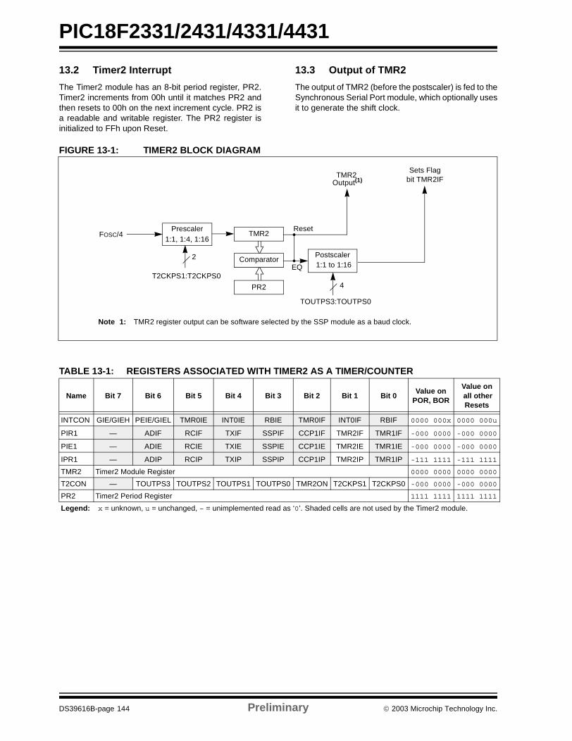
PIC18F2331/2431/4331/4431
13.2 Timer2 Interrupt
The Timer2 module has an 8-bit period register, PR2.Timer2 increments from 00h until it matches PR2 andthen resets to 00h on the next increment cycle. PR2 isa readable and writable register. The PR2 register isinitialized to FFh upon Reset.
13.3 Output of TMR2
The output of TMR2 (before the postscaler) is fed to theSynchronous Serial Port module, which optionally usesit to generate the shift clock.
FIGURE 13-1: TIMER2 BLOCK DIAGRAM
TABLE 13-1: REGISTERS ASSOCIATED WITH TIMER2 AS A TIMER/COUNTER
Comparator
TMR2Sets Flag
TMR2
Output(1)
Reset
Postscaler
Prescaler
PR2
2
FOSC/4
1:1 to 1:16
1:1, 1:4, 1:16
EQ
4
bit TMR2IF
Note 1: TMR2 register output can be software selected by the SSP module as a baud clock.
TOUTPS3:TOUTPS0
T2CKPS1:T2CKPS0
Name Bit 7 Bit 6 Bit 5 Bit 4 Bit 3 Bit 2 Bit 1 Bit 0Value on
POR, BOR
Value on all other Resets
INTCON GIE/GIEH PEIE/GIEL TMR0IE INT0IE RBIE TMR0IF INT0IF RBIF 0000 000x 0000 000u
PIR1 — ADIF RCIF TXIF SSPIF CCP1IF TMR2IF TMR1IF -000 0000 -000 0000
PIE1 — ADIE RCIE TXIE SSPIE CCP1IE TMR2IE TMR1IE -000 0000 -000 0000
IPR1 — ADIP RCIP TXIP SSPIP CCP1IP TMR2IP TMR1IP -111 1111 -111 1111
TMR2 Timer2 Module Register 0000 0000 0000 0000
T2CON — TOUTPS3 TOUTPS2 TOUTPS1 TOUTPS0 TMR2ON T2CKPS1 T2CKPS0 -000 0000 -000 0000
PR2 Timer2 Period Register 1111 1111 1111 1111
Legend: x = unknown, u = unchanged, – = unimplemented read as ‘0’. Shaded cells are not used by the Timer2 module.
DS39616B-page 144 Preliminary 2003 Microchip Technology Inc.

PIC18F2331/2431/4331/4431
14.0 TIMER5 MODULE
The Timer5 module implements these features:
• 16-bit timer/counter operation• Synchronous and asynchronous counter modes• Continuous and Single-Shot operating modes
• Four programmable prescaler values (1:1 to 1:8)• Interrupt generated on period match• Special event trigger Reset function
• Double-buffered registers• Operation during Sleep• CPU wake-up from Sleep
• Selectable hardware Reset input with a wake-up feature
Timer5 is a general-purpose timer/counter that incorpo-rates additional features for use with the Motion Feed-back module (see Section 16.0 “Motion FeedbackModule”). It may also be used as a general-purposetimer or a special event trigger delay timer. When usedas a general-purpose timer, it can be configured to gen-erate a delayed special event trigger (e.g., an ADCspecial event trigger) using a pre-programmed perioddelay.
Timer5 is controlled through the Timer5 Control Regis-ter (T5CON), shown in Register 14-1. The timer can beenabled or disabled by setting or clearing the control bitTMR5ON (T5CON<0>).
A block diagram of Timer5 is shown in Figure 14-1.
REGISTER 14-1: T5CON: TIMER5 CONTROL REGISTER R/W-0 R/W-0 R/W-0 R/W-0 R/W-0 R/W-0 R/W-0 R/W-0
T5SEN RESEN T5MOD T5PS1 T5PS0 T5SYNC TMR5CS TMR5ON
bit 7 bit 0
bit 7 T5SEN: Timer5 Sleep Enable bit(1)
1 = Timer5 enabled during Sleep0 = Timer5 disabled during Sleep
bit 6 RESEN: Special Event Reset Enable bit
1 = Special Event Reset disabled0 = Special Event Reset enabled
bit 5 T5MOD: Timer5 Mode bit1 = Single-Shot mode enabled0 = Continuous Count mode enabled
bit 4:3 T5PS1:T5PS0: Timer5 Input Clock Prescale Select bits11 =1:810 =1:401 =1:200 =1:1
bit 2 T5SYNC: Timer5 External Clock Input Synchronization Select bitWhen TMR5CS = 1: 1 = Do not synchronize external clock input 0 = Synchronize external clock inputWhen TMR5CS = 0: This bit is ignored. Timer5 uses the internal clock when TMR5CS = 0
bit 1 TMR5CS: Timer5 Clock Source Select bit
1 = External clock from pin T5CKI0 = Internal clock (TCY)
bit 0 TMR5ON: Timer5 On bit1 = Timer5 enabled0 = Timer5 disabled
Note 1: For Timer5 to operate during Sleep mode, T5SYNC must be set.
Legend:
R = Readable bit W = Writable bit U = Unimplemented bit, read as ‘0’
- n = Value at POR ‘1’ = Bit is set ‘0’ = Bit is cleared x = Bit is unknown
2003 Microchip Technology Inc. Preliminary DS39616B-page 145

PIC18F2331/2431/4331/4431
FIGURE 14-1: TIMER5 BLOCK DIAGRAM (16-BIT READ/WRITE MODE SHOWN)
14.1 Timer5 Operation
Timer5 combines two 8-bit registers to function as a 16-bit timer. The TMR5L register is the actual low byte ofthe timer; it can be read and written to directly. The highbyte is contained in an unmapped register; it is readand written to through TMR5H, which serves as abuffer. Each register increments from 00h to FFh.
A second register pair, PR5H and PR5L, serves as aperiod register; it sets the maximum count for theTMR5 register pair. When TMR5 reaches the value ofPR5, the timer rolls over to 00h and sets the TMR5IFinterrupt flag. A simplified block diagram of the Timer5module is shown in Figure 2-1.
Timer5 supports three configurations:
• 16-bit Synchronous Timer • 16-bit Synchronous Counter • 16-bit Asynchronous Counter
In Synchronous Timer configuration, the timer isclocked by the internal device clock. The optionalTimer5 prescaler divides the input by 2, 4, 8, or not atall (1:1). The TMR5 register pair increments on Q1.Clearing TMR5CS (= 0) selects the internal deviceclock as the timer sampling clock.
In Synchronous Counter configuration, the timer isclocked by the external clock (T5CKI) with the optionalprescaler. The external T5CKI is selected by setting theTMR5CS bit (TMR5CS = 1); the internal clock isselected by clearing TMR5CS. The external clock issynchronized to the internal clock by clearing theT5SYNC bit. The input on T5CKI is sampled on everyQ2 and Q4 of the internal clock. The low to risetransition is decoded on three adjacent samples and
T5SYNC
TMR5CS
T5PS1:T5PS0
Sleep Input
FOSC/4InternalClock
Prescaler1, 2, 4, 8
Synchronize
detect
1
02
T5CKI1
0
TMR5L
Internal Data Bus
TMR5
TMR5H
High Byte
8
8
Write TMR5L
Read TMR5L
8
TMR5ON
On/OffTimer5
NoiseFilter
PR5L
16
PR5H
8
8
Comparator
16
8
1
0
TMR5
PR5
ResetLogic
SpecialEventLogic
Timer5 Reset
Set TMR5IF
Timer5 Reset(external)
Special Event Trigger Output
Special EventTrigger Inputfrom IC1
Note: The TIMER5 may be used as a generalpurpose timer and as the time baseresource to the Motion Feedback module(Input Capture or Quadrature EncoderInterface).
DS39616B-page 146 Preliminary 2003 Microchip Technology Inc.

PIC18F2331/2431/4331/4431
the Timer5 is incremented on the next Q1. The T5CKIminimum pulse width high and low time must begreater than TCY/2.
In Asynchronous Counter configuration, Timer5 isclocked by the external clock (T5CKI) with the optionalprescaler. In this mode, T5CKI is not synchronized tothe internal clock. By setting TMR5CS, the externalinput clock (T5CKI) can be used as the counter sam-pling clock. When T5SYNC is set, the external clock isnot synchronized to the internal device clock.
The timer count is not reset automatically when themodule is disabled. The user may write the counterregister to initialize the counter.
14.1.1 CONTINUOUS AND SINGLE-SHOT OPERATION
Timer5 has two operating modes: Continuous-countand Single-shot.
Continuous-count mode is selected by clearing theT5MOD control bit (= 0). In this mode, the Timer5 timebase will start incrementing according to the prescalersettings until a TMR5/PR5 match occurs, or until TMR5rolls over (FFFFh to 0000h). The TMR5IF interrupt flagis set, the TMR5 register is reset on the following inputclock edge, and the timer continues to count for as longas the TMR5ON bit remains set.
Single-shot mode is selected by setting T5MOD (= 1).In this mode, the Timer5 time base begins to incrementaccording to the prescaler settings until a TMR5/PR5match occurs. This causes the TMR5IF interrupt flag tobe set, the TMR5 register pair to be cleared on thefollowing input clock edge, and the TMR5ON bit to becleared by the hardware to halt the timer.
The Timer5 time base can only start incrementing inSingle-shot mode under two conditions:
1. Timer5 is enabled (TMR5ON is set), or
2. Timer5 is disabled, and a Special Event Resettrigger is present on the Timer5 reset input. (SeeSection 14.7 “Timer5 Special Event ResetInput” for additional information).
14.2 16-bit Read/Write and Write Modes
As noted, the actual high byte of the Timer5 registerpair is mapped to TMR5H, which serves as a buffer.Reading TMR5L will load the contents of the high byteof the register pair into the TMR5H register. This allowsthe user to accurately read all 16 bits of the registerpair, without having to determine whether a read of thehigh byte followed by the low byte is valid due to arollover between reads.
Since the actual high byte of the Timer5 register pair isnot directly readable or writable, it must be read andwritten to through the Timer5 High Byte Buffer register(TMR5H). The T5 high byte is updated with the con-tents of TMR5H when a write occurs to TMR5L. Thisallows a user to write all 16 bits to both the high and lowbytes of Timer5 at once. Writes to TMR5H do not clearthe Timer5 prescaler. The prescaler is only cleared onwrites to TMR5L.
14.2.1 16-BIT READ-MODIFY-WRITE
Read-modify-write instructions like BSF and BCF willread the contents of a register, make the appropriatechanges, and place the result back into the register.The write portion of a read-modify-write instruction ofTMR5H will not update the contents of the high byte ofTMR5 until a write of TMR5L takes place. Only then willthe contents of TMR5H be placed into the high byte ofTMR5.
14.3 Timer5 Prescaler
The Timer5 clock input (either TCY or the external clock)may be divided by using the Timer5 programmableprescaler. The prescaler control bits T5PS1:T5PS0(T5CON<4:3>) select a prescale factor of 2, 4, 8 or noprescale.
The Timer5 prescaler is cleared by any of the following:
• A write to the Timer5 register• Disabling Timer5 (TMR5ON = 0)• A device Reset such as Master Clear, POR or
BOR
14.4 Noise Filter
The Timer5 module includes an optional input noisefilter, designed to reduce spurious signals in noisyoperating environments. The filter ensures that theinput is not permitted to change until a stable value hasbeen registered for three consecutive sampling clockcycles.
The noise filter is part of the input filter network associ-ated with the Motion Feedback Module (seeSection 16.0 “Motion Feedback Module”). All of thefilters are controlled using the Digital Filter Control(DFLTCON) register (Register 16-3). The Timer5 filtercan be individually enabled or disabled by setting orclearing the FLT4EN bit (DFLTCON<7>). It is disabledon all BOR and BOR resets.
For additional information, refer to Section 16.3“Noise Filters” in the Motion Feedback module.
Note: The Timer5 module does NOT preventwrites to the PR5 registers (PR5H:PR5L)while the timer is enabled. Writing to PR5while the timer is enabled may result inunexpected period match events.
Note: Writing to the T5CON register does notclear the Timer5.
2003 Microchip Technology Inc. Preliminary DS39616B-page 147

PIC18F2331/2431/4331/4431
14.5 Timer5 Interrupt
Timer5 has the ability to generate an interrupt on aperiod match. When the PR5 register is loaded with anew period value (00FFh), the Timer5 time base incre-ments until its value is equal to the value of PR5. Whena match occurs, the Timer5 interrupt is generated onthe rising edge of Q4; TMR5IF is set on the next TCY.
The interrupt latency (i.e., the time elapsed from themoment Timer5 rolls over until TMR5IF is set) will notexceed 1 TCY. When the Timer5 clock input isprescaled and a TMR5/PR5 match occurs, the interruptwill be generated on the first Q4 rising edge after TMR5resets.
14.6 Timer5 Special Event Trigger Output
A Timer5 special event trigger is generated on a TMR5/PR5 match. The special event trigger is generated onthe falling edge of Q3.
Timer5 must be configured for either Synchronousmode (counter or timer) to take advantage of thespecial event trigger feature. If Timer5 is running inAsynchronous Counter mode, the special event triggermay not work and should not be used.
14.7 Timer5 Special Event Reset Input
In addition to the special event output, Timer5 has aSpecial Event Reset input that may be used with InputCapture channel 1 (IC1) of the Motion Feedbackmodule. To use the Special Event Reset, the Capture 1Control register CAP1CON must be configured for oneof the special event trigger modes (CAP1M3:CAP1M0= 1110 or 1111). The Special Event Reset trigger canbe disabled by setting the RESEN control bit(T5CON<6>).
The Special Event Reset resets the Timer5 time base.This reset occurs in either Continuous-count or Single-shot modes.
14.7.1 WAKE-UP ON IC1 EDGE
The Timer5 Special Event Reset input can act as aTimer5 wake-up and a start-up pulse. Timer5 must bein Single-shot mode and disabled (TMR5ON = 0). Anactive edge on the CAP1 input pin will set TMR5ON;the timer is subsequently incremented on the next fol-lowing clock according to the prescaler and the Timer5clock settings. A subsequent hardware time-out (suchas TMR5/PR5 match) will clear the TMR5ON bit andstop the timer.
14.7.2 DELAYED-ACTION EVENT TRIGGER
An active edge on CAP1 can also be used to initiatesome later action delayed by the Timer5 time base. Inthis case, Timer5 increments as before after beingtriggered. When the hardware time-out occurs, thespecial event trigger output is generated and used totrigger another action, such as an A/D conversion. Thisallows a given hardware action to be referenced from acapture edge on CAP1 and delayed by the timer.
The event timing for the delayed action event trigger isdiscussed further in Section 16.1 “Input Capture”.
14.7.3 SPECIAL EVENT RESET WHILE TIMER5 IS INCREMENTING
In the event that a bus write to Timer5 coincides with aSpecial Event Reset trigger, the bus write will alwaystake precedence over Special Event Reset trigger.
14.8 Operation in Sleep Mode
When Timer5 is configured for asynchronous opera-tion, it will continue to increment each timer clock (orprescale multiple of clocks). Executing the SLEEPinstruction will either stop the timer or let the timer con-tinue, depending on the setting of the Timer5 SleepEnable bit, T5SE. If T5SE is set (= 1), the timer contin-ues to run when the SLEEP instruction is executed andthe external clock is selected (TMR5CS = 1). If T5SE iscleared, the timer stops when a SLEEP instruction isexecuted, regardless of the state of the GTPCS bit.
To summarize, Timer5 will continue to increment whena SLEEP instruction is executed only if all of these bitsare set:
• TMR5ON
• T5SE• TMR5CS• T5SYNC
14.8.1 INTERRUPT DETECT IN SLEEP MODE
When configured as described above, Timer5 willcontinue to increment on each rising edge on T5CKIwhile in Sleep mode. When a TMR5/PR5 matchoccurs, an interrupt is generated which can wake thepart.
DS39616B-page 148 Preliminary 2003 Microchip Technology Inc.

PIC18F2331/2431/4331/4431
TABLE 14-1: REGISTERS ASSOCIATED WITH TIMER5
Name Bit 7 Bit 6 Bit 5 Bit 4 Bit 3 Bit 2 Bit 1 Bit 0Value on: POR, BOR
Value on all other
Resets
INTCON GIE/GIEH PEIE/GIEL TMR0IE INT0IE RBIE TMR0IF INT0IF RBIF 0000 000x 0000 000u
IPR3 — — — PTIP IC3DRIP IC2QEIP IC1IP TMR5IP ---1 1111 ---1 1111
PIE3 — — — PTIE IC3DRIE IC2QEIE IC1IE TMR5IE ---0 0000 ---0 0000
PIR3 — — — PTIF IC3DRIF IC2QEIF IC1IF TMR5IF ---0 0000 ---0 0000
TMR5H Timer5 Register High Byte xxxx xxxx uuuu uuuu
TMR5L TImer5 Register Low Byte xxxx xxxx uuuu uuuu
PR5H Timer5 Period Register High Byte 1111 1111 1111 1111
PR5L Timer5 Period Register Low Byte 1111 1111 1111 1111
T5CON T5SEN RESEN T5MOD T5PS1 T5PS0 T5SYNC TMR5CS TMR5ON 0000 0000 0000 0000
CAP1CON — CAP1REN — — CAP1M3 CAP1M2 CAP1M1 CAP1M0 -1-- 0000 -1-0 0000
DFLTCON — FLT4EN FLT3EN FLT2EN FLT1EN FLTCK2 FLTCK1 FLTCK0 -000 0000 -000 0000
Legend: x = unknown, u = unchanged, – = unimplemented.
2003 Microchip Technology Inc. Preliminary DS39616B-page 149

PIC18F2331/2431/4331/4431
NOTES:
DS39616B-page 150 Preliminary 2003 Microchip Technology Inc.

PIC18F2331/2431/4331/4431
15.0 CAPTURE/COMPARE/PWM (CCP) MODULES
The CCP (Capture/Compare/PWM) module contains a16-bit register that can operate as a 16-bit Capture reg-ister, a 16-bit Compare register or a PWM Master/SlaveDuty Cycle register. Table 15-1 shows the timerresources required for each of the CCP module modes.
The operation of CCP1 is identical to that of CCP2, withthe exception of the special event trigger. Therefore,operation of a CCP module is described with respect toCCP1, except where noted.
REGISTER 15-1: CCPxCON: CCP MODULE CONTROL REGISTER U-0 U-0 R/W-0 R/W-0 R/W-0 R/W-0 R/W-0 R/W-0
— — DCxB1 DCxB0 CCPxM3 CCPxM2 CCPxM1 CCPxM0
bit 7 bit 0
bit 7-6 Unimplemented: Read as ‘0’
bit 5-4 DCxB1:DCxB0: PWM Duty Cycle bit1 and bit0Capture mode:UnusedCompare mode:UnusedPWM mode:These bits are the two LSbs (bit 1 and bit 0) of the 10-bit PWM duty cycle. The upper eight bits (DCx9:DCx2) of the duty cycle are found in CCPRxL.
bit 3-0 CCPxM3:CCPxM0: CCPx Mode Select bits
0000 =Capture/Compare/PWM disabled (resets CCPx module) 0001 =Reserved 0010 =Compare mode, toggle output on match (CCPxIF bit is set) 0011 =Reserved 0100 =Capture mode, every falling edge 0101 =Capture mode, every rising edge0110 =Capture mode, every 4th rising edge 0111 =Capture mode, every 16th rising edge1000 =Compare mode, Initialize CCP pin Low, on compare match force CCP pin High
(CCPxIF bit is set) 1001 =Compare mode, Initialize CCP pin High, on compare match force CCP pin Low
(CCPxIF bit is set) 1010 =Compare mode, Generate software interrupt-on-compare match (CCPxIF bit is set,
CCP pin is unaffected) 1011 =Compare mode, Trigger special event (CCP2IF bit is set) 11xx =PWM mode
Legend:
R = Readable bit W = Writable bit U = Unimplemented bit, read as ‘0’
- n = Value at POR ‘1’ = Bit is set ‘0’ = Bit is cleared x = Bit is unknown
2003 Microchip Technology Inc. Preliminary DS39616B-page 151

PIC18F2331/2431/4331/4431
15.1 CCP1 Module
Capture/Compare/PWM Register 1 (CCPR1) iscomprised of two 8-bit registers: CCPR1L (low byte)and CCPR1H (high byte). The CCP1CON registercontrols the operation of CCP1. All are readable andwritable.
TABLE 15-1: CCP MODE – TIMER RESOURCE
15.2 CCP2 Module
Capture/Compare/PWM Register2 (CCPR2) is com-prised of two 8-bit registers: CCPR2L (low byte) andCCPR2H (high byte). The CCP2CON register controlsthe operation of CCP2. All are readable and writable.
CCP Mode Timer Resource
CaptureCompare
PWM
Timer1Timer1Timer2
DS39616B-page 152 Preliminary 2003 Microchip Technology Inc.

PIC18F2331/2431/4331/4431
15.3 Capture Mode
In Capture mode, CCPR1H:CCPR1L captures the 16-bit value of the TMR1 register when an event occurs onpin RC2/CCP1. An event is defined as one of thefollowing:
• every falling edge
• every rising edge• every 4th rising edge• every 16th rising edge
The event is selected by control bits CCP1M3:CCP1M0(CCP1CON<3:0>). When a capture is made, theinterrupt request flag bit CCP1IF (PIR1<2>) is set; itmust be cleared in software. If another capture occursbefore the value in register CCPR1 is read, the oldcaptured value is overwritten by the new captured value.
15.3.1 CCP PIN CONFIGURATION
In Capture mode, the RC2/CCP1 pin should beconfigured as an input by setting the TRISC<2> bit.
15.3.2 TIMER1 MODE SELECTION
Timer 1 must be running in Timer mode or Synchro-nized Counter mode to be used with the capture fea-ture. In Asynchronous Counter mode, the captureoperation may not work.
15.3.3 SOFTWARE INTERRUPT
When the Capture mode is changed, a false captureinterrupt may be generated. The user should keep bitCCP1IE (PIE1<2>) clear to avoid false interrupts andshould clear the flag bit, CCP1IF, following any suchchange in operating mode.
15.3.4 CCP PRESCALER
There are four prescaler settings, specified by bitsCCP1M3:CCP1M0. Whenever the CCP module isturned off or the CCP module is not in Capture mode,the prescaler counter is cleared. This means that anyReset will clear the prescaler counter.
Switching from one capture prescaler to another maygenerate an interrupt. Also, the prescaler counter willnot be cleared, therefore, the first capture may be froma non-zero prescaler. Example 15-1 shows the recom-mended method for switching between capture pres-calers. This example also clears the prescaler counterand will not generate the “false” interrupt.
EXAMPLE 15-1: CHANGING BETWEEN CAPTURE PRESCALERS
FIGURE 15-1: CAPTURE MODE OPERATION BLOCK DIAGRAM
Note: If the RC2/CCP1 is configured as an out-put, a write to the port can cause a capturecondition.
CLRF CCP1CON, F ; Turn CCP module offMOVLW NEW_CAPT_PS ; Load WREG with the
; new prescaler mode; value and CCP ON
MOVWF CCP1CON ; Load CCP1CON with; this value
CCPR1H CCPR1L
TMR1H TMR1L
Set Flag bit CCP1IF
Q’sCCP1CON<3:0>
CCP1 pin
Prescaler÷ 1, 4, 16
andEdge Detect
TMR1Enable
CCPR2H CCPR2L
TMR1H TMR1L
Set Flag bit CCP2IF
Q’sCCP2CON<3:0>
CCP2 pin
Prescaler÷ 1, 4, 16
andEdge Detect
TMR1Enable
2003 Microchip Technology Inc. Preliminary DS39616B-page 153

PIC18F2331/2431/4331/4431
15.4 Compare Mode
In Compare mode, the 16-bit CCPR1 (CCPR2) registervalue is constantly compared against the TMR1register pair value. When a match occurs, the RC2/CCP1 (RC1/CCP2) pin:
• Is driven High
• Is driven Low• Toggles output (High-to-Low or Low-to-High) • Remains unchanged (interrupt only)
The action on the pin is based on the value of controlbits CCP1M3:CCP1M0 (CCP2M3:CCP2M0). At thesame time, interrupt flag bit CCP1IF (CCP2IF) is set.
15.4.1 CCP PIN CONFIGURATION
The user must configure the CCPx pin as an output byclearing the appropriate TRISC bit.
15.4.2 TIMER1 MODE SELECTION
Timer1 must be running in Timer mode or Synchro-nized Counter mode if the CCP module is using thecompare feature. In Asynchronous Counter mode, thecompare operation may not work.
15.4.3 SOFTWARE INTERRUPT MODE
When generate software interrupt is chosen, the CCP1pin is not affected. Only a CCP interrupt is generated (ifenabled).
15.4.4 SPECIAL EVENT TRIGGER
In this mode, an internal hardware trigger is generated,which may be used to initiate an action.
The special event trigger output of CCP1 resets theTMR1 register pair. This allows the CCPR1 register toeffectively be a 16-bit programmable period register forTimer1.
The special trigger output of CCP2 resets the TMR1register pair. Additionally, the CCP2 special eventtrigger will start an A/D conversion if the A/D module isenabled.
FIGURE 15-2: COMPARE MODE OPERATION BLOCK DIAGRAM
Note: Clearing the CCP1CON register will forcethe RC2/CCP1 compare output latch tothe default low level. This is not thePORTC I/O data latch.
Note: The special event trigger from the CCP2module will not set the Timer1 interruptflag bit.
CCPR1H CCPR1L
TMR1H TMR1L
ComparatorQ S
R
OutputLogic
Special Event Trigger
Set Flag bit CCP1IF
MatchRC2/CCP1 pin
TRISC<2>CCP1CON<3:0>
Mode SelectOutput Enable
Special Event Trigger will:Reset Timer1, but not set Timer1 interrupt flag bit,and set bit GO/DONE (ADCON0<2>), which starts an A/D conversion (CCP2 only)
CCPR2H CCPR2L
ComparatorQ S
R
OutputLogic
Special Event Trigger
Set Flag bit CCP2IF
MatchRC1/CCP2 pin
TRISC<1>CCP2CON<3:0>
Mode SelectOutput Enable
DS39616B-page 154 Preliminary 2003 Microchip Technology Inc.

PIC18F2331/2431/4331/4431
TABLE 15-2: REGISTERS ASSOCIATED WITH CAPTURE, COMPARE AND TIMER1
Name Bit 7 Bit 6 Bit 5 Bit 4 Bit 3 Bit 2 Bit 1 Bit 0Value on
POR, BOR
Value onall otherResets
INTCON GIE/GIEH PEIE/GIEL TMR0IE INT0IE RBIE TMR0IF INT0IF RBIF 0000 000x 0000 000u
PIR1 — ADIF RCIF TXIF SSPIF CCP1IF TMR2IF TMR1IF -000 0000 -000 0000
PIE1 — ADIE RCIE TXIE SSPIE CCP1IE TMR2IE TMR1IE -000 0000 -000 0000
IPR1 — ADIP RCIP TXIP SSPIP CCP1IP TMR2IP TMR1IP -111 1111 -111 1111
TRISC PORTC Data Direction Register 1111 1111 1111 1111
TMR1L Holding Register for the Least Significant Byte of the 16-bit TMR1 Register xxxx xxxx uuuu uuuu
TMR1H Holding Register for the Most Significant Byte of the 16-bit TMR1 Register xxxx xxxx uuuu uuuu
T1CON RD16 T1RUN T1CKPS1 T1CKPS0 T1OSCEN T1SYNC TMR1CS TMR1ON 0000 0000 uuuu uuuu
CCPR1L Capture/Compare/PWM Register1 (LSB) xxxx xxxx uuuu uuuu
CCPR1H Capture/Compare/PWM Register1 (MSB) xxxx xxxx uuuu uuuu
CCP1CON — — DC1B1 DC1B0 CCP1M3 CCP1M2 CCP1M1 CCP1M0 --00 0000 --00 0000
CCPR2L Capture/Compare/PWM Register2 (LSB) xxxx xxxx uuuu uuuu
CCPR2H Capture/Compare/PWM Register2 (MSB) xxxx xxxx uuuu uuuu
CCP2CON — — DC2B1 DC2B0 CCP2M3 CCP2M2 CCP2M1 CCP2M0 --00 0000 --00 0000
PIR2 OSCFIF CMIF — EEIF BCLIF LVDIF TMR3IF CCP2IF 00-0 0000 00-0 0000
PIE2 OSCFIE CMIE — EEIE BCLIE LVDIE TMR3IE CCP2IE 00-0 0000 00-0 0000
IPR2 OSCFIP CMIP — EEIP BCLIP LVDIP TMR3IP CCP2IP 11-1 1111 11-1 1111
Legend: x = unknown, u = unchanged, — = unimplemented, read as ‘0’. Shaded cells are not used by Capture and Timer1.
2003 Microchip Technology Inc. Preliminary DS39616B-page 155

PIC18F2331/2431/4331/4431
15.5 PWM Mode
In Pulse Width Modulation (PWM) mode, the CCP1 pinproduces up to a 10-bit resolution PWM output. Sincethe CCP1 pin is multiplexed with the PORTC data latch,the TRISC<2> bit must be cleared to make the CCP1pin an output.
Figure 15-3 shows a simplified block diagram of theCCP module in PWM mode.
For a step-by-step procedure on how to set up the CCPmodule for PWM operation, see Section 15.5.3“Setup for PWM Operation”.
FIGURE 15-3: SIMPLIFIED PWM BLOCK DIAGRAM
A PWM output (Figure 15-4) has a time base(period) and a time that the output is high (dutycycle). The frequency of the PWM is the inverse ofthe period (1/period).
FIGURE 15-4: PWM OUTPUT
15.5.1 PWM PERIOD
The PWM period is specified by writing to the PR2register. The PWM period can be calculated using thefollowing equation.
EQUATION 15-1:
PWM frequency is defined as 1/[PWM period]. WhenTMR2 is equal to PR2, the following three events occuron the next increment cycle:
• TMR2 is cleared• The CCP1 pin is set (if PWM duty cycle = 0%, the
CCP1 pin will not be set)• The PWM duty cycle is copied from CCPR1L into
CCPR1H
15.5.2 PWM DUTY CYCLE
The PWM duty cycle is specified by writing to theCCPR1L register and to the CCP1CON<5:4> bits. Upto 10-bit resolution is available. The CCPR1L containsthe eight MSbs and the CCP1CON<5:4> contains thetwo LSbs. This 10-bit value is represented byCCPR1L:CCP1CON<5:4>. The PWM duty cycle iscalculated by the following equation.
EQUATION 15-2:
CCPR1L and CCP1CON<5:4> can be written to at anytime, but the duty cycle value is not copied intoCCPR1H until a match between PR2 and TMR2 occurs(i.e., the period is complete). In PWM mode, CCPR1His a read-only register.
Note: Clearing the CCP1CON register will forcethe CCP1 PWM output latch to the defaultlow level. This is not the PORTC I/O datalatch.
CCPR1L
CCPR1H (Slave)
Comparator
TMR2
Comparator
PR2
(Note 1)
R Q
S
Duty Cycle Registers CCP1CON<5:4>
Clear Timer,CCP1 pin and latch D.C.
TRISC<2>
RC2/CCP1
Note: 8-bit timer is concatenated with 2-bit internal Q clock or 2 bits of the prescaler to create 10-bit time base.
Period
Duty Cycle
TMR2 = PR2
TMR2 = Duty Cycle
TMR2 = PR2
Note: The Timer2 postscaler (see Section 13.0“Timer2 Module”) is not used in the deter-mination of the PWM frequency. Thepostscaler could be used to have a servoupdate rate at a different frequency thanthe PWM output.
PWM period = [(PR2) + 1] • 4 • TOSC •(TMR2 prescale value)
PWM duty cycle = (CCPR1L:CCP1CON<5:4>) •Tosc • (TMR2 prescale value)
DS39616B-page 156 Preliminary 2003 Microchip Technology Inc.

PIC18F2331/2431/4331/4431
The CCPR1H register and a 2-bit internal latch areused to double buffer the PWM duty cycle. This doublebuffering is essential for glitchless PWM operation.When the CCPR1H and 2-bit latch match TMR2,concatenated with an internal 2-bit Q clock or two bitsof the TMR2 prescaler, the CCP1 pin is cleared. Themaximum PWM resolution (bits) for a given PWMfrequency is given by the following equation.
EQUATION 15-3:
15.5.3 SETUP FOR PWM OPERATION
The following steps should be taken when configuringthe CCP module for PWM operation:
1. Set the PWM period by writing to the PR2 register.2. Set the PWM duty cycle by writing to the CCPR1L
register and CCP1CON<5:4> bits.3. Make the CCP1 pin an output by clearing the
TRISC<2> bit.4. Set the TMR2 prescale value and enable Timer2
by writing to T2CON.5. Configure the CCP1 module for PWM operation.
TABLE 15-3: EXAMPLE PWM FREQUENCIES AND RESOLUTIONS AT 40 MHz
TABLE 15-4: REGISTERS ASSOCIATED WITH PWM AND TIMER2
Note: If the PWM duty cycle value is longer thanthe PWM period, the CCP1 pin will not becleared.
PWM Resolution (max) =
FOSC
FPWMlog
log(2)bits
PWM Frequency 2.44 kHz 9.77 kHz 39.06 kHz 156.25 kHz 312.50 kHz 416.67 kHz
Timer Prescaler (1, 4, 16) 16 4 1 1 1 1
PR2 Value FFh FFh FFh 3Fh 1Fh 17h
Maximum Resolution (bits) 10 10 10 8 7 6.58
Name Bit 7 Bit 6 Bit 5 Bit 4 Bit 3 Bit 2 Bit 1 Bit 0Value on
POR,BOR
Value on all otherResets
INTCON GIE/GIEH PEIE/GIEL TMR0IE INT0IE RBIE TMR0IF INT0IF RBIF 0000 000x 0000 000u
PIR1 — ADIF RCIF TXIF SSPIF CCP1IF TMR2IF TMR1IF -000 0000 -000 0000
PIE1 — ADIE RCIE TXIE SSPIE CCP1IE TMR2IE TMR1IE -000 0000 -000 0000
IPR1 — ADIP RCIP TXIP SSPIP CCP1IP TMR2IP TMR1IP -111 1111 -111 1111
TRISC PORTC Data Direction Register 1111 1111 1111 1111
TMR2 Timer2 Module Register 0000 0000 0000 0000
PR2 Timer2 Module Period Register 1111 1111 1111 1111
T2CON — TOUTPS3 TOUTPS2 TOUTPS1 TOUTPS0 TMR2ON T2CKPS1 T2CKPS0 -000 0000 -000 0000
CCPR1L Capture/Compare/PWM Register1 (LSB) xxxx xxxx uuuu uuuu
CCPR1H Capture/Compare/PWM Register1 (MSB) xxxx xxxx uuuu uuuu
CCP1CON — — DC1B1 DC1B0 CCP1M3 CCP1M2 CCP1M1 CCP1M0 --00 0000 --00 0000
CCPR2L Capture/Compare/PWM Register2 (LSB) xxxx xxxx uuuu uuuu
CCPR2H Capture/Compare/PWM Register2 (MSB) xxxx xxxx uuuu uuuu
CCP2CON — — DC2B1 DC2B0 CCP2M3 CCP2M2 CCP2M1 CCP2M0 --00 0000 --00 0000
Legend: x = unknown, u = unchanged, – = unimplemented, read as ‘0’. Shaded cells are not used by PWM and Timer2.
2003 Microchip Technology Inc. Preliminary DS39616B-page 157

PIC18F2331/2431/4331/4431
NOTES:
DS39616B-page 158 Preliminary 2003 Microchip Technology Inc.

PIC18F2331/2431/4331/4431
16.0 MOTION FEEDBACK MODULE
The Motion Feedback module is a special-purposeperipheral designed for motion feedback applications.Together with the Power Control PWM module (seeSection 17.0 “Power Control PWM Module”), it pro-vides a variety of control solutions for a wide range ofelectric motors.
The module actually consists of two hardwaresub-modules:
• Input Capture module (IC)• Quadrature Encoder Interface (QEI).
Together with Timer5 (see Section 14.0 “Timer5 Mod-ule”), these modules provide a number of options formotion and control applications.
Many of the features for the IC and QEI submodulesare fully programmable, creating a flexible peripheralstructure that can accommodate a wide range ofin-system uses. An overview of the available featuresis presented in Table 16-1. A simplified block diagramof the entire Motion Feedback module is shown inFigure 16-1.
TABLE 16-1: SUMMARY OF MOTION FEEDBACK MODULE FEATURES
Note: Because the same input pins are commonto the IC and QEI submodules, only one ofthese two submodules may be used at anygiven time. If both modules are on, the QEIsubmodule will take precedence.
Submodule Mode(s) Features Timer Function
IC (3x) • Synchronous• Input Capture
• Flexible input capture modes• Available prescaler• Selectable time base reset• Special event trigger for ADC
sampling/conversion or optional TMR5 Reset feature (CAP1 only)
• Wake-up from Sleep function• Selectable interrupt frequency• Optional noise filter
TMR5 • 3x Input Capture (edge capture, pulse width, period measurement, capture on change)
• Special event triggers the A/D conversion on the CAP1 input
QEI QEI • Detect position• Detect direction of rotation• Large bandwidth (Fcy/16)• Optional noise filter
16-bit position counter
• Position measurement • Direction of rotation status
Velocity measurement
• 2x and 4x update modes• Velocity event postscaler• Counter overflow flag for low
rotation speed• Utilizes Input Capture 1 logic
(IC1)• High and low velocity support
TMR5 • Precise velocity measurement• Direction of rotation status
2003 Microchip Technology Inc. Preliminary DS39616B-page 159

PIC18F2331/2431/4331/4431
FIGURE 16-1: MOTION FEEDBACK MODULE BLOCK DIAGRAM
TCY
Timer5
T5CKI
Clock
Dat
a B
us<
7:0>
TMR5<15:0>
CAP1/INDX
CAP2/QEA
CAP3/QEB
TMR5<15:0>
TCY
ClockQEIF
Special Reset Trigger
IC3IF
TMR5IF
8
8
8
8
IC2IF
IC1IF
8
8
Position Counter
QEIControlLogic
Divider
IC1
IC2
Special Event output
Direction
Pre
scal
erP
resc
aler
Pre
scal
er
Velocity Event
Postscaler
IC3
Filter
Filter
Filter
Special Reset Trigger
QEB
QEA
INDX
3x Input Capture Logic
QEI Logic
8
TMR5Reset
ControlTimer Reset
Timer reset
CHGIF
CHGIF
IC3IF
IC2IF
QEIF
8QEIMode
Decoder
IC3DRIF
IC2QEIF
Filter
DS39616B-page 160 Preliminary 2003 Microchip Technology Inc.

PIC18F2331/2431/4331/4431
16.1 Input Capture
The Input Capture (IC) submodule implements thefollowing features:
• Three channels of independent input capture (16-bits/channel) on the CAP1, CAP2 and CAP3 pins
• Edge-trigger, period or pulse width measurement operating modes for each channel
• Programmable prescaler on every input capture channel
• Special event trigger output (IC1 only)• Selectable noise filters on each capture input
Input channel (IC1) includes a special event triggerthat can be configured for use in Velocity Measure-ment mode. Its block diagram is shown in Figure 16-2.IC2 and IC3 are similar, but lack the special event trig-ger features or additional velocity-measurement logic.A representative block diagram is shown inFigure 16-3. Please note that the time base is Timer5.
FIGURE 16-2: INPUT CAPTURE BLOCK DIAGRAM FOR IC1
CAP1BUF/VELR(1)
CA
PxR
EN
andModeSelect
Prescaler1, 4, 16
CAP1 Pin
CAP1M<3:0> Q clocks
34
FLTCK<2:0>
VELM
Noise Filter
TMR5
Timer5 ResetTimerReset Control
Clock
Q Clocks CAP1M<3:0>
MUXFirst Event
CAP1BUF_clk
Reset
1
0
IC1_TR
Timer5 Logic
ResetControl
Reset
velcap(2)
Clock/Reset/InterruptDecodeLogic
SpecialEventReset
IC1IF
Note 1: CAP1BUF register is reconfigured as VELR register when QEI mode is active.
2: QEI generated velocity pulses, vel_out, are downsampled to produce this velocity capture signal.
2003 Microchip Technology Inc. Preliminary DS39616B-page 161

PIC18F2331/2431/4331/4431
FIGURE 16-3: INPUT CAPTURE BLOCK DIAGRAM FOR IC2 AND IC3
CAPxBUF(1,2,3)
CAPxREN(2)
andModeSelect
Prescaler1, 4, 16
CAP2/CAP3 Pin
CAPxM<3:0>(1)
Q’s3
4FLTCK<2:0>
Noise Filter TMR5
Enable
TMR5
TMR5 ResetTimerReset Control
CaptureClock
ICxIF(1)
Capture Clock/
Q clocks CAPxM<3:0>(1)
CAPxBUF_clk(1)
Reset
Reset/InterruptDecodeLogic
Note 1: IC2 and IC3 are denoted as x=2 and 3.
2: CAP2BUF is enabled as POSCNT when QEI mode is active.
3: CAP3BUF is enabled as MAXCNT when QEI mode is active.
DS39616B-page 162 Preliminary 2003 Microchip Technology Inc.

PIC18F2331/2431/4331/4431
The three Input Capture channels are controlledthrough the Input Capture Control RegistersCAP1CON, CAP2CON, and CAP3CON. Each channelis configured independently with its dedicated register.The implementation of the registers is identical, exceptfor the Special Event trigger (see Section 16.1.8 “Spe-cial Event Trigger (CAP1 Only)”). The typical CaptureControl register is shown in Register 16-1.
REGISTER 16-1: CAPxCON: INPUT CAPTURE CONTROL REGISTER
When in Counter mode, the counter must beconfigured as the synchronous counter only(TMR5SYNC = 0). When configured in Asynchronousmode, the IC module will not work properly.
U-0 R/W-0 U-0 R/W-0 R/W-0 R/W-0 R/W-0 R/W-0
— CAPxREN — — CAPxM3 CAPxM2 CAPxM1 CAPxM0
bit 7 bit 0
bit 7 Unimplemented: Read as ‘0’
bit 6 CAPxREN: Time Base Reset Enable bit1 = Enabled 0 = Disable selected time base Reset on capture.
bit 5 Unimplemented: Read as ‘0’
bit 4 Unimplemented: Read as ‘0’
bit 3-0 CAPxM3:CAPxM0: Input Capture 1 (ICx) Mode Select bits1111 = Special Event Trigger mode. The trigger occurs on every rising edge on CAP1 input(1)
1110 = Special Event Trigger mode. The trigger occurs on every falling edge on CAP1 input(1)
1101 = Unused1100 = Unused1011 = Unused1010 = Unused1001 = Unused1000 = Capture on every CAPx input state change0111 = Pulse Width Measurement mode, every rising to falling edge0110 = Pulse Width Measurement mode, every falling to rising edge0101 = Frequency Measurement mode, every rising edge0100 = Capture mode, every 16th rising edge0011 = Capture mode, every 4th rising edge0010 = Capture mode, every rising edge0001 = Capture mode, every falling edge0000 = Input Capture 1 (ICx) off
Note 1: Special Event Trigger is only available on CAP1. For CAP2 and CAP3, this config-uration is unused.
Legend:
R = Readable bit W = Writable bit U = Unimplemented bit, read as ‘0’
- n = Value at POR ‘1’ = Bit is set ‘0’ = Bit is cleared x = Bit is unknown
Note: Throughout this section, references toregisters and bit names that may be asso-ciated with a specific capture channel willbe referred to generically by the use of theterm ‘x’ in place of the channel number.For example, ‘CAPxREN’ may refer to theCapture Reset Enable bit in CAP1CON,CAP2CON or CAP3CON.
2003 Microchip Technology Inc. Preliminary DS39616B-page 163

PIC18F2331/2431/4331/4431
16.1.1 EDGE CAPTURE MODE
In this mode, the value of the time base is capturedeither on every rising edge, every falling edge, every4th rising edge, or every 16th rising edge. The edgepresent on the input capture pin (CAP1, CAP2 orCAP3) is sampled by the synchronizing latch. Thesignal is used to load the input capture buffer (ICxBUFregister) on the following Q1 clock (see Figure 16-4).Consequently, Timer5 is either reset to ‘0’ (Q1immediately following the capture event) or left freerunning, depending on the setting of Capture ResetEnable, CAPxREN, in the CAPxCON register.
FIGURE 16-4: EDGE CAPTURE MODE TIMING
Note 1: Input capture prescalers are reset(cleared) when the Input Capture moduleis disabled (CAPxM = 0000).
2: When the Input Capture mode is changedwithout first disabling the module andentering the new Input Capture mode, afalse interrupt (or special event trigger onIC1) may be generated. The user shouldeither (1) disable the Input Capture beforeentering another mode or (2) disable ICinterrupts to avoid false interrupts duringIC mode changes.
3: During IC mode changes, the prescalercount will not be cleared, therefore thefirst capture in the new IC mode may befrom the non-zero prescaler.
Note: On the first capture edge following thesetting of the Input Capture mode (i.e.,MOVWF CAP1CON), Timer5 contents arealways captured into the correspondinginput capture buffer (i.e., CAPxBUF).Timer5 can optionally be reset; however,this is dependent on the setting of theCapture Reset Enable bit (CAPxREN),see Figure 16-4.
CAP1 pin(2)
0000 0002 0000 0001 0002TMR5(1)
CAP1BUF(3) 0002
001400130012 0015
ABCD
0001
0003
TMR5 reset(4)
MOVWF CAP1CON BCF CAP1CON, CAP1REN
Note 5
0016
Instruction
Note 1: TMR5 is a synchronous time base input to the Input Capture, prescaler = 1:1. It increments on Q1 rising edge.
2: IC1 is configured in Edge Capture mode (CAP1M3:CAP1M0 = 0010) with the time base reset upon edge capture(CAP1REN = 1) and no noise filter.
3: TMR5 value is latched by CAP1BUF on TCY. In the event that a write to TMR5 coincides with an input capture event,the write will always take precedence. All input capture buffers, CAP1BUF, CAP2BUF and CAP3BUF, are updated withthe incremented value of the time base on the next TCY clock edge when the capture event takes place (see Note 4when Reset occurs).
4: TMR5 Reset is normally an asynchronous reset signal to TMR5. When used with the input capture, it is active immedi-ately after the time base value is captured.
5: TMR5 Reset pulse is disabled by clearing CAP1REN bit (e.g, BCF CAP1CON, CAP1REN).
OSC
Execution
Q1Q2Q3Q4 Q1Q2Q3Q4Q1Q2Q3Q4Q1Q2Q3Q4Q1Q2Q3Q4Q1Q2Q3Q4Q1Q2Q3Q4Q1Q2Q3Q4Q1Q2Q3Q4 Q1Q2Q3Q4
DS39616B-page 164 Preliminary 2003 Microchip Technology Inc.

PIC18F2331/2431/4331/4431
16.1.2 PERIOD MEASUREMENT MODE
The Period Measurement mode is selected by settingCAPxM3:CAPxM0 = 0101. In this mode, the value ofTimer5 is latched into the CAPxBUF register on the ris-ing edge of the input capture trigger and Timer5 is sub-sequently reset to 0000h (optional by settingCAPxREN = 1) on the next TCY (see capture and resetrelationship in Figure 16-4).
16.1.3 PULSE WIDTH MEASUREMENT MODE
The Pulse Width Measurement mode can be config-ured for two different edge sequences, such that thepulse width is based on either the falling to rising edge
of the CAPx input pin (CAPxM3:CAPxM0 = 0110), oron the rising to falling edge (CAPxM3:CAPxM0 =0111).
Timer5 is always reset on the edge when themeasurement is first initiated. For example, when themeasurement is based on the falling to rising edge,Timer5 is first reset on the falling edge and the timervalue is captured on the rising edge thereafter. Uponentry into the Pulse Width Measurement mode, thevery first edge detected on the CAPx pin is alwayscaptured. The TMR5 value is reset on the first activeedge (see Figure 16-5).
FIGURE 16-5: PULSE WIDTH MEASUREMENT MODE TIMING
CAP1 pin(2)
0000 0002 0000 0001 0002TMR5(1)
CAP1BUF(3) 0002
001400130012 0015
0015
0001
TMR5 reset(4,5)
MOVWF CAP1CONInstruction
0001
Note 1: TMR5 is a synchronous time base input to the Input Capture, prescaler = 1:1. It increments on every Q1 rising edge.
2: IC1 is configured in Pulse Width Measurement mode (CAP1M3:CAP1M0 = 0111, rising to falling pulse width measure-ment). No noise filter on CAP1 input is used. MOVWF instruction loads CAP1CON when W = 0111.
3: TMR5 value is latched by CAP1BUF on TCY rising edge. In the event that a write to TMR5 coincides with an input cap-ture event, the write will always take precedence. All input capture buffers, CAP1BUF, CAP2BUF and CAP3BUF, areupdated with the incremented value of the time base on the next TCY clock edge when the capture event takes place(see Note 4 when Reset occurs).
4: TMR5 Reset is normally an asynchronous Reset signal to TMR5. When used in Pulse Width Measurement mode, it isalways present on the edge that first initiates the pulse width measurement (i.e., when configured in the rising to fallingPulse Width Measurement mode, it is active on each rising edge detected. In the falling to rising Pulse Width Measure-ment mode, it is active on each falling edge detected.
5: TMR5 Reset pulse is activated on the capture edge. CAP1REN bit has no bearing in this mode.
Execution(2)
Q1Q2Q3Q4Q1Q2Q3Q4Q1Q2Q3Q4Q1Q2Q3Q4Q1Q2Q3Q4Q1Q2Q3Q4Q1Q2Q3Q4Q1Q2Q3Q4Q1Q2Q3Q4 Q1Q2Q3Q4
2003 Microchip Technology Inc. Preliminary DS39616B-page 165

PIC18F2331/2431/4331/4431
16.1.3.1 Pulse Width Measurement Timing
Pulse width measurement accuracy can be onlyensured when the pulse width high and low present onCAPx input exceeds one TCY clock cycle. Thelimitations depend on the mode selected:
• When CAPxM3:CAPxM0 = 0110 (rising-to-falling edge delay), the CAPx input high pulse width (TccH) must exceed TCY + 10 ns.
• When CAPxM3:CAPxM0 = 0111 (falling-to-rising edge delay), the CAPx input low pulse width (TccL) must exceed TCY + 10 ns.
16.1.4 INPUT CAPTURE ON STATE CHANGE
When CAPxM3:CAPxM0 = 1000, the value is capturedon every signal change on the CAPx input. If all threecapture channels are configured in this mode, thethree-input-capture can be used as the Hall-effectsensor state transition detector. The value of Timer5can be captured, Timer5 reset and the interruptgenerated. Any change on CAP1, CAP2 or CAP3 isdetected and the associated time base count iscaptured.
For position and velocity measurement in this mode,the timer can be optionally reset (see Section 16.1.6“Timer5 Reset” for Reset options).
FIGURE 16-6: INPUT CAPTURE ON STATE CHANGE (HALL-EFFECT SENSOR MODE)
Note 1: The Period Measurement mode willproduce valid results upon sampling ofthe second rising edge of the inputcapture. CAPxBUF values latched duringthe first active edge after initialization areinvalid.
2: The Pulse Width Measurement mode willlatch the value of the timer upon samplingof the first input signal edge by the inputcapture.
CAP2
CAP1
CAP3
Time Base(1)
CAP1BUF(2)
CAP2BUF(2)
CAP3BUF(2)
0FFFh
0000h
Time Base Reset(1)
1
0
1
1
0
0
1
1
0
0
1
0
0
1
1
0
0
1
Sta
te 1
Sta
te 2
Sta
te 3
Sta
te 4
Sta
te 5
Sta
te 6
Note 1: TMR5 can be selected as the time base for input capture. Time base can be optionally reset when the capture resetenabled bit is set (CAPXREN = 1).
2: Detailed CAPxBUF event timing (all modes reflect same capture and Reset timing) is shown in Figure 16-4.There aresix commutation BLDC hall-effect sensor states shown. The other two remaining states (i.e., 000h and 111h) areinvalid in the normal operation. They are still to be decoded by the CPU firmware in BLDC motor application.
DS39616B-page 166 Preliminary 2003 Microchip Technology Inc.

PIC18F2331/2431/4331/4431
16.1.5 ENTERING INPUT CAPTURE MODE AND CAPTURE TIMING
The following is a summary of functional operationupon entering any of the Input Capture modes:
1. After the module is configured for one of thecapture modes by setting the Mode Select bits(CAPxM3:CAPxM0), the first detected edgecaptures Timer5 value and stores it in the CAPx-BUF register. The timer is then reset (dependingon the setting of CAPxREN bit) and starts toincrement according to its settings, seeFigure 16-4, Figure 16-5 and Figure 16-6.
2. On all edges, the capture logic performs the fol-lowing:a) Input Capture mode is decoded and the
active edge is identifiedb) The CAPxREN bit is checked to determine
whether Timer5 is reset or not.c) On every active edge, the Timer5 value is
recorded in the input capture buffer (CAPx-BUF).
d) Reset Timer5 after capturing the value ofthe timer when CAPxREN bit is enabled.Timer5 is reset on every active captureedge in this case.
e) On all continuing capture edge eventsrepeat steps 1 through 4 until the Opera-tional mode is terminated either by userfirmware, POR or BOR.
f) The timer value is not affected when switch-ing into and out of various input capturemodes.
16.1.6 TIMER5 RESET
Every Input Capture trigger can optionally reset(TMR5). Capture Reset Enable bit, CAPxREN, gatesthe automatic Reset of the time base of the captureevent with this enable Reset signal. All capture eventsreset the selected timer when CAPxREN is set. Resetsare disabled when CAPxREN is cleared (seeFigure 16-4, Figure 16-5 and Figure 16-6).
16.1.7 IC INTERRUPTS
There are four operating modes for which the ICmodule can generate an interrupt and set one of theInterrupt Capture flag bits (IC1IF, IC2QEIF orIC3DRIF). The interrupt flag that is set depends on thechannel in which the event occurs. The modes are:
• Edge capture (CAPxM3:CAPxM0 = 0001, 0010, 0011 or 0100)
• Period measurement event (CAPxM3:CAPxM0 = 0101)
• Pulse width measurement event (CAPxM3:CAPxM0 = 0110 or 0111)
• State change event (CAPxM3:CAPxM0 = 1000)
The timing of interrupt and special trigger events isshown in Figure 16-7. Any active edge is detected onthe rising edge of Q2 and propagated on the risingedge of Q4 rising edge. If an active edge happens tooccur any later than this (on the falling edge of Q2, forexample), then it will be recognized on the next Q2rising edge.
Note: The CAPxREN bit has no effect in PulseWidth Measurement mode.
Note: The special event trigger is generated onlyin the Special Event Trigger mode onCAP1 input (CAP1M2:CAP1M0> = 1110and 1111). IC1IF interrupt is not set in thismode.
2003 Microchip Technology Inc. Preliminary DS39616B-page 167

PIC18F2331/2431/4331/4431
FIGURE 16-7: CAPXIF INTERRUPTS AND IC1 SPECIAL EVENT TRIGGER
16.1.8 SPECIAL EVENT TRIGGER (CAP1 ONLY)
The Special Event Trigger mode of IC1(CAP1M3:CAP1M0 = 1110 or 1111) enables theSpecial Event Trigger signal. The trigger signal can beused as the Special Event Reset input to TMR5,resetting the timer when the specific event happens onIC1. The events are summarized in Table 16-2.
TABLE 16-2: SPECIAL EVENT TRIGGER
16.1.9 OPERATING MODES SUMMARY
Table 16-3 shows a summary of the input capture con-figuration when used in conjunction with TMR5 timerresource.
16.1.10 OTHER OPERATING MODES
Although the IC and QEI submodules are mutuallyexclusive, the IC can be reconfigured to work with theQEI module to perform specific functions. In effect, theQEI “borrows” hardware from the IC to perform theseoperations.
For velocity measurement, the QEI uses dedicatedhardware in channel IC1. The CAP1BUF registers areremapped, becoming the VREG registers. Its operationand use are described in Section 16.2.6 “VelocityMeasurement”.
While in QEI mode, the CAP2BUF and CAP3BUF reg-isters of channel IC2 and IC3 are used for positiondetermination. They are remapped as the POSCNTand MAXCNT buffer registers, respectively.
Q2Q1 Q3 Q4Q2Q1 Q3 Q4 Q2Q1 Q3 Q4 Q2Q1 Q3 Q4 Q2Q1 Q3 Q4
OSC
CAP1 pin
IC1IF
TMR5
TMR5 Reset
XXXX 0000 0001
TMR5ON(1)
Note 1: Timer5 is only reset and enabled (assuming: TMR5ON = 0 and TMR5MOD = 1) when the Special Event Reset Triggeris enabled for the Timer5 Reset input. TMR5ON bit is asserted and Timer5 is reset on the Q1 rising edge following theevent capture. With the Special Event Reset Trigger disabled, Timer5 cannot be reset by the Special Event ResetTrigger on CAP1 input. In order for the Special Event Reset Trigger to work as the Reset trigger to Timer5, IC1 must beconfigured in the Special Event Trigger mode (CAP1M<3:0> = 1110 or 1111).
CAP1M3:CAP1M0
Description
1110 The trigger occurs on every falling edge on CAP1 input
1111 The trigger occurs on every rising edge on CAP1 input
DS39616B-page 168 Preliminary 2003 Microchip Technology Inc.

PIC18F2331/2431/4331/4431
TABLE 16-3: INPUT CAPTURE TIME BASE RESET SUMMARY
Pin CAPxM Mode TimerReset Timer on Capture
Description
CAP1 0001-0100 Edge Capture TMR5 optional(1) Simple edge Capture mode (includes aselectable prescaler)
0101 Period Measurement TMR5 optional(1) Captures Timer5 on period boundaries0110-0111 Pulse Width
MeasurementTMR5 always Captures Timer5 on pulse boundaries
1000 Input Capture on State Change
TMR5 optional(1) Captures Timer5 on state change
1110-1111 Special Event Trigger(rising or falling edge)
TMR5 optional(2) Used as a special event trigger to be usedwith the Timer5 or other peripheralmodules
CAP2 0001-0100 Edge Capture TMR5 optional(1) Simple edge Capture mode (includes aselectable prescaler
0101 Period Measurement TMR5 optional(1) Captures Timer5 on period boundaries0110-0111 Pulse Width
MeasurementTMR5 always Captures Timer5 on pulse boundaries
1000 Input Capture on State Change
TMR5 optional(1) Captures Timer5 on state change
CAP3 0001-0100 Edge Capture TMR5 optional(1) Simple edge Capture mode (includes aselectable prescaler
0101 Period Measurement TMR5 optional(1) Captures Timer5 on period boundaries
0110-0111 Pulse Width Measurement
TMR5 always Captures Timer5 on pulse boundaries
1000 Input Capture on State Change
TMR5 optional(1) Captures Timer5 on state change
Note 1: Timer5 may be reset on capture events only when CAPxRE = 1. 2: Trigger mode will not reset Timer5 unless RESEN = 0 in the T5CON register.
2003 Microchip Technology Inc. Preliminary DS39616B-page 169

PIC18F2331/2431/4331/4431
16.2 Quadrature Encoder Interface
The Quadrature Encoder Interface (QEI) decodesspeed and motion sensor information. It can be used inany application that uses a quadrature encoder forfeedback. The interface implements these features:
• Three QEI inputs: two phase signals (QEA and QEB) and one index signal (INDX)
• Direction of movement detection with a direction change interrupt (IC3DRIF)
• 16-bit up/down position counter
• Standard and high-precision position tracking modes
• Two position update modes (x2 and x4)• Velocity measurement with a programmable
postscaler for high-speed velocity measurement• Position counter interrupt (IC2QEIF in the PIR3
register)• Velocity control interrupt (IC1IF in the PIR3
register)
The QEI sub-module has three main components: theQEI control logic block, the position counter andvelocity postscaler.
The QEI control logic detects the leading edge on theQEA or QEB phase input pins, and generates the countpulse which is sent to the position counter logic. It alsosamples the index input signal (INDX), and generatesthe direction of rotation signal (up/down) and the veloc-ity event signals.
The position counter acts as an integrator for trackingdistance traveled. The QEA and QEB input edgesserve as the stimulus to create the input clock whichadvances the Position Counter Register (POSCNT).The register is incremented on either the QEA inputedge, or the QEA and QEB input edges, depending onthe operating mode. It is reset either by a rollover onmatch to the Period Register, MAXCNT, or on the exter-nal index pulse input signal (INDX). An interrupt is gen-erated on a reset of POSCNT if the position counterinterrupt is enabled.
The velocity postscaler down-samples the velocitypulses used to increment the velocity counter by aspecified ratio. It essentially divides down the numberof velocity pulses to one output per so many input, pre-serving the pulse width in the process.
A simplified block-diagram of the QEI module is shownin Figure 16-8.
FIGURE 16-8: QEI BLOCK DIAGRAM
Comparator
CAP2/QEA
CAP1/INDX
CAP3/QEB
POSCNT/CAP2BUF
Reset on match
QEI Module
QEIControlLogic
Filter
Filter
Filter
QEB
QEA
INDX
Timer reset
Velocity Event Postscaler 8
MAXCNT/CAP3BUF
8
8
ClockDirection 8
8
Set IC2QEIF
Set UP/DOWN
Dat
a B
us
Position Counter
Reset Timer5Direction change Set CHGIF
Velocity Capture
DS39616B-page 170 Preliminary 2003 Microchip Technology Inc.

PIC18F2331/2431/4331/4431
16.2.1 QEI CONFIGURATION
The QEI module shares its input pins with the InputCapture module. The inputs are mutually exclusive;only the IC module or the QEI module (but not both)can be enabled at one time. Also, because the IC andQEI are multiplexed to the same input pins, theprogrammable noise filters can be dedicated to onemodule only.
The operation of the QEI is controlled by the QEICONconfiguration register. See Register 16-2.
REGISTER 16-2: QEICON: QUADRATURE ENCODER INTERFACE CONTROL REGISTER
Note: In the event that both QEI and IC areenabled, QEI will take precedence and ICwill remain disabled.
R/W-0 R/W-0 R-0 R/W-0 R/W-0 R/W-0 R/W-0 R/W-0VELM ERROR UP/DOWN QEIM2 QEIM1 QEIM0 PDEC1 PDEC0
bit 7 bit 0
bit 7 VELM: Velocity Mode bit1 = Velocity mode disabled0 = Velocity mode enabled
bit 6 ERROR: QEI error bit(1)
1 = Position counter(4) overflow or underflow0 = No overflow or underflow
bit 5 UP/DOWN: Direction of Rotation Status bit(1)
1 = Forward0 = Reverse
bit 4-2 QEIM2:QEIM0: QEI Mode bits(2,3)
111 =Unused110 =QEI enabled in 4x Update mode; position counter reset on period match
(POSCNT = MAXCNT)101 =QEI enabled in 4x Update mode; INDX resets the position counter100 =Unused010 =QEI enabled in 2x Update mode; position counter reset on period match
(POSCNT = MAXCNT)001 =QEI enabled in 2x Update mode; INDX resets the position counter000 =QEI off
bit 1-0 PDEC1:PDEC0: Velocity Pulse Reduction Ratio bit11 =1:6410 =1:1601 =1:400 =1:1
Note 1: QEI must be enabled and in Index mode.
2: QEI mode select must be cleared (= 000) to enable CAP1, CAP2 or CAP3 inputs. If QEI andIC modules are both enabled, QEI will take precedence.
3: Enabling one of the QEI operating modes remaps the IC buffer registers CAP1BUFH,CAP1BUFL, CAP2BUFH, CAP2BUFL, CAP3BUFH and CAP3BUFL as the VREGH,VREGL, POSCNTH, POSCNTL, MAXCNTH, and MAXCNTL registers (respectively) for theQEI.
4: ERROR bit must be cleared in software.
Legend:
R = Readable bit W = Writable bit U = Unimplemented bit, read as ‘0’
-n = Value at POR ‘1’ = bit is set ‘0’ = bit is cleared x = bit is unknown
2003 Microchip Technology Inc. Preliminary DS39616B-page 171

PIC18F2331/2431/4331/4431
16.2.2 QEI MODES
Position measurement resolution depends on howoften the Position Counter register, POSCNT, isincremented. There are two QEI update modes tomeasure the rotor’s position: QEI x2 and QEI x4.
TABLE 16-4: QEI MODES
16.2.2.1 QEI x2 Update Mode
QEI x2 Update mode is selected by setting the QEIMode Select bits (QEIM2:QEIM0) to ‘001’ or ‘010’. Inthis mode, the QEI logic detects every edge on theQEA input only. Every rising and falling edge on theQEA signal clocks the position counter.
The position counter can be reset by either an input onthe INDX pin (QEIM2:QEIM0 = 001), or by aperiod-match, even when the POSCNT register pairequals MAXCNT (QEIM2:QEIM0 = 010).
16.2.2.2 QEI 4x Update Mode
QEI x4 Update mode provides for a finer resolution ofthe rotor position, since the counter increments ordecrements more frequently for each QEA/QEB inputpulse pair than in QEI x2 mode. This mode is selectedby setting the QEI Mode Select bits to 101 or 110. InQEI x4, the phase measurement is made on the risingand the falling edges of both QEA and QEB inputs. Theposition counter is clocked on every QEA and QEBedge.
Like QEI x2 mode, the position counter can be reset byan input on the pin (QEIM2:QEIM0 = 101), or by theperiod-match event (QEIM2:QEIM0 = 010).
16.2.3 QEI OPERATION
The Position Counter register pair (POSCNTH:POSCNTL) acts as an integrator, whose value is pro-portional to the position of the sensor rotor that corre-sponds to the number of active edges detected.POSCNT can either increment or decrement, depend-ing on a number of selectable factors which aredecoded by the QEI logic block. These include theCount mode selected, the phase relationship of QEA toQEB (“lead/lag”), the direction of rotation, and if a resetevent occurs. The logic is detailed in the sections thatfollow.
16.2.3.1 Edge and Phase Detect
In the first step, the active edges of QEA and QEB aredetected, and the phase relationship between them isdetermined. The position counter is changed based onthe selected QEI mode.
In QEI x2 Update mode, the position counter incre-ments or decrements on every QEA edge based on thephase relationship of the QEA and QEB signals.
In QEI x4 Update mode, the position counterincrements or decrements on every QEA and QEBedge based on the phase relationship of the QEA andQEB signals. For example, if QEA leads QEB, theposition counter is incremented by 1. If QEB lags QEA,the position counter is decremented by 1.
16.2.3.2 Direction of Count
The QEI control logic generates a signal that setsthe UP/DOWN bit (QEICON<5>); this in turndetermines the direction of the count. When QEAleads QEB, UP/DOWN is set (= 1), and the positioncounter increments on every active edge. WhenQEA lags QEB, UP/DOWN is cleared, and theposition counter decrements on every active edge.
TABLE 16-5: DIRECTION OF ROTATION
QEIM2:QEIM0
Mode/Reset
Description
000 — QEI disabled(1)
001 x2 update/ index pulse
Two clocks per QEA pulse. INDX resets POSCNT.
010 x2 update/ period match
Two clocks per QEA pulse. POSCNT reset by the period match (MAXCNT).
011 — unused100 — unused101 x4 update/
indexFour clocks per QEA and QEB pulse pair. INDX resets POSCNT.
110 x4 update/ period match
Four clocks per QEA and QEB pulse pair.POSCNT reset by the period match (MAXCNT).
111 — unused
Note 1: QEI module is disabled. The position counter and the velocity measurement functions are fully disabled in this mode.
Current Signal
Detected
Previous Signal Detected
Pos. Cntrl.(1)Rising Falling
QEA QEB QEA QEB
QEA rising x INCx DEC
QEA falling x DEC
x INCQEB rising x INC
x DEC
QEB falling x INCx DEC
Note 1: When UP/DOWN = 1, the position counter is incremented; when UP/DOWN = 0, the position counter is decremented.
DS39616B-page 172 Preliminary 2003 Microchip Technology Inc.

PIC18F2331/2431/4331/4431
16.2.3.3 Reset and Update Events
The position counter will continue to increment or dec-rement until one of the following events takes place.The type of event and the direction of rotation when ithappens determines if a register reset or updateoccurs.
1. An index pulse is detected on the INDX input(QEIM2:QEIM0 = 001).
If the encoder is traveling in the forward direc-tion, POSCNT is reset (00h) on the next clockedge after the index marker, INDX, has beendetected. The position counter resets on theQEA or QEB edge once the INDX rising edgehas been detected.
If the encoder is traveling in the reverse direc-tion, the value in the MAXCNT register is loadedinto POSCNT on the next quadrature pulseedge (QEA or QEB) after the falling edge onINDX has been detected.
2. A POSTCNT/MAXCNT period match occurs(QEIM2:QEIM0 = 010).
If the encoder is traveling in the forward direc-tion, POSCNT is reset (00h) on the next clockedge when POSCNT = MAXCNT. An interruptevent is triggered on the next TCY after the reset(see Figure 16-10)
If the encoder is traveling in the reversedirection and the value of POSCNT reaches00h, POSCNT is loaded with the contents ofMAXCNT register on the next clock edge. Aninterrupt event is triggered on the next TCY afterthe load operation (see Figure 16-10).
The value of the position counter is not affected duringQEI mode changes, nor when the QEI is disabledaltogether.
16.2.4 QEI INTERRUPTS
The position counter interrupt occurs, and the interruptflag (IC2QEIF) is set, based on the following events:
• A POSCNT/MAXCNT period match event (QEIM2:QEIM0 = 010 or 110)
• A POSCNT rollover (FFFFh to 0000h) in Period mode only (QEIM2:QEIM0 = 010 or 110)
• An index pulse detected on INDX.
The interrupt timing diagrams for IC2QEIF are shown inFigure 16-10 and Figure 16-11.
When the direction has changed, the direction changeInterrupt flag (IC3DRIF) is set on the following TCY
clock (see Figure 16-10).
If the position counter rolls over in Index mode, theERROR bit will be set.
16.2.5 QEI SAMPLE TIMING
The quadrature input signals, QEA and QEB, may varyin quadrature frequency. The minimum quadratureinput period TQEI is 16TCY.
The position count rate, FPOS, is directly proportional tothe rotor’s RPM, line count D and QEI Update mode (x2vs. x4); that is,
The maximum position count rate (i.e., 4x QEIUpdate mode, D = 1024) with FCY = 10 MIPS is equalto 2.5 MHz, which corresponds to FQEI of 625 kHz.
Figure 16-9 shows QEA and QEB quadrature inputstiming when sampled by the noise filter.
Note: The number of incremental lines in theposition encoder is typically set at D = 1024 and the QEI Update mode = x4.
FPOS4D RPM⋅
60------------------------=
2003 Microchip Technology Inc. Preliminary DS39616B-page 173

PIC18F2331/2431/4331/4431
FIGURE 16-9: QEI INPUTS WHEN SAMPLED BY THE FILTER (DIVIDE RATIO = 1:1)
FIGURE 16-10: QEI MODULE RESET TIMING ON PERIOD MATCH
TCY
QEA pin
TGD = 3TCY
QEB pin
QEA input
QEB input
TQEI = 16TCY(1)
Note 1: The module design allows a quadrature frequency of up to FQEI = FCY/16.
QEB
QEA
UP/DOWN
IC2QEIF
POSCNT(1)
1520
1521
1522
1523
1524
1525
1526
1527
count (+/-) +1 +1 +1 +1 +1 +1 +1 +1 +1 +1 +1 +1 -1 -1 -1 -1 -1 -1 -1 -1 -1 -1 -1 -1 -1 -1 -1 -1 -1 -1 -1 -1 -1 -1 -1 -1
MAXCNT MAXCNT=1527
0000
0001
0002
0003
0004
0003
0002
0001
0000
1527
1526
1525
1524
1523
1522
1521
1520
1519
1518
1517
1516
1515
1514
Q4(3) Q4(3)
Q1(4) Q1(5)positioncounter load
Forward Reverse
Q1(5)IC3DRIF
Note 2 Note 2
Note 1: POSCNT register is shown in QEI x4 Update mode (POSCNT increments on every rising and every falling edge ofQEA and QEB input signals). Asynchronous external QEA and QEB input are synchronized to TCY clock by the inputsampling FF in the noise filter (see Figure 16-14).
2: When POSCNT = MAXCNT, POSCNT is reset to ‘0’ on the next QEA rising edge. POSCNT is set to MAXCNT whenPOSCNT = 0 (when decrementing), which occurs on the next QEA falling edge.
3: IC2QEI is generated on Q4 rising edge.
4: Position counter is loaded with ‘0’ (which is a rollover event in this case) on POSCNT = MAXCNT.
5: Position counter is loaded with MAXCNT value (1527h) on underflow.
6: IC2QEIF must be cleared in software.
Note 6
DS39616B-page 174 Preliminary 2003 Microchip Technology Inc.

PIC18F2331/2431/4331/4431
FIGURE 16-11: QEI MODULE RESET TIMING WITH THE INDEX INPUT
16.2.6 VELOCITY MEASUREMENT
The velocity pulse generator, in conjunction with theIC1 and the synchronous TMR5 (in synchronousoperation), provides a method for high accuracy speedmeasurements at both low and high mechanical motorspeeds. The Velocity mode is enabled when the VELMbit is cleared (= 0) and QEI is set to one of its operatingmodes (see Table 16-6).
To optimize register space, the input capture channelone (IC1) is used to capture TMR5 counter values.Input capture buffer register, CAP1BUF, is redefined inVelocity Measurement mode, VELM = 0, as theVelocity Register buffer (VREGH, VREGL).
TABLE 16-6: VELOCITY PULSES
QEB
QEA
UP/DOWN
IC2QEIF
POSCNT(1)
1520
1521
1522
1523
1524
1525
1526
1527
count (+/-) +1 +1 +1 +1 +1 +1 +1 +1 +1 +1 +1 +1 -1 -1 -1 -1 -1 -1 -1 -1 -1 -1 -1 -1 -1 -1 -1 -1 -1 -1 -1 -1 -1 -1 -1 -1
MAXCNT MAXCNT=1527
0000
0001
0002
0003
0004
0003
0002
0001
0000
1527
1526
1525
1524
1523
1522
1521
1520
1519
1518
1517
1516
1515
1514
Q4(3) Q4(3)
INDX
Q1(4) Q1(5)Positioncounter load
Forward Reverse
Note 2 Note 2
Note 1: POSCNT register is shown in QEI x4 Update mode (POSCNT increments on every rising and every falling edge ofQEA and QEB input signals)
2: When INDX Reset pulse is detected, POSCNT is reset to ‘0’ on the next QEA or QEB edge. POSCNT is set toMAXCNT when POSCNT = 0 (when decrementing), which occurs on the next QEA or QEB edge. Similar Resetsequence occurs for the reverse direction except that the INDX signal is recognized on its falling edge. The Resetis generated on the next QEA or QEB edge.
3: IC2QEI is enabled for one TCY clock cycle.
4: Position counter is loaded with ‘0000h’ (i.e., Reset) on the next QEA or QEB edge when INDX is high.
5: Position counter is loaded with MAXCNT value (e.g., 1527h) on the next QEA or QEB edge following the INDXfalling edge input signal detect).
6: IC2QEIF must be cleared in software.
Note 6
QEIM<2:0> Velocity Event Mode
001010
x2 Velocity Event mode. The velocity pulse is generated on every QEA edge.
101110
x4 Velocity Event mode. The velocity pulse is generated on every QEA and QEB active edge.
2003 Microchip Technology Inc. Preliminary DS39616B-page 175

PIC18F2331/2431/4331/4431
16.2.6.1 Velocity Event Timing
The event pulses are reduced by a fixed ratio by thevelocity pulse divider. The divider is useful forhigh-speed measurements where the velocity eventshappen frequently. By producing a single output pulsefor a given number of input event pulses, the countercan track larger pulse counts (i.e., distance travelled)for a given time interval. Time is measured by utilizingthe TMR5 time base.
Each velocity pulse serves as a capture pulse. With theTMR5 in Synchronous Timer mode, the value of TMR5is captured on every output pulse of the postscaler. Thecounter is subsequently reset to ‘0’. TMR5 is resetupon a capture event.
Figure 16-13 shows the velocity measurement timingdiagram.
FIGURE 16-12: VELOCITY MEASUREMENT BLOCK DIAGRAM
CAP2/QEA
CAP1/INDX
CAP3/QEB
QEIControlLogic
QEB
QEA
INDX
Postscaler
Clock
DirectionPositionCounter
TMR5
IC1
No
ise
Filt
ers
ResetLogic
16
Velocity Mode
(VELR Register)
TCYClockTMR5 Reset
Velocity CaptureVelocity Event
DS39616B-page 176 Preliminary 2003 Microchip Technology Inc.

PIC18F2331/2431/4331/4431
FIGURE 16-13: VELOCITY MEASUREMENT TIMING(1)
16.2.6.2 Velocity Postscaler
The velocity event pulse (velcap, see Figure 16-12)serves as the TMR5 capture trigger to IC1 while in theVelocity mode. The number of velocity events arereduced by the velocity postscaler before they are usedas the input capture clock. The velocity event reductionratio can be set with the PDEC1:PDEC0 control bits(QEICON<1:0>) to 1:4, 1:16, 1:64 or no reduction (1:1).
The velocity postscaler settings are automaticallyreloaded from their previous values as the Velocitymode is re-enabled.
16.2.6.3 CAP1REN in Velocity Mode
The TMR5 value can be reset (TMR5 register pair =0000h) on a velocity event capture by setting theCAP1REN bit (CAP1CON<6>). When CAP1REN iscleared, the TMR5 time base will not be reset on anyvelocity event capture pulse. The VELR register pair,however, will continue to be updated with the currentTMR5 value.
QEB
QEA
cnt_reset(3)
TMR5(2)
velcap
BCF TMR5CON, VELM
VELR(2)
1520
1521
1522
1523
1525
1526
1527
1528
1529
1530
1531
1532
1534
1535
1536
0000
0001
0002
0003
0004
0005
0006
0007
0008
0009
0000
0001
0002
0003
0004
152915
24
1533
1537
vel_out
Old Value
Forward
Q1Q1
IC1IF(4)
Q1
Instr.Execution MOVWF QEICON(5) BCF PIE2, IC1IE BSF PIE2, IC1IE
CAP1REN
Note 1: Timing shown is for QEIM<2:0> = 101, 110 or 111 (x4 Update mode enabled) and the velocity postscaler divide ratiois set to divide by 4 (PDEC<1:0> = 01).
2: VELR register latches the TMR5 count on the “velcap” capture pulse. Timer5 must be set to the synchronous timer orCounter mode. In this example, it is set to the Synchronous Timer mode where the TMR5 prescaler divide ratio = 1 (i.e., Timer5 clock = TCY).
3: The TMR5 counter is reset on the next Q1 clock cycle following the “velcap” pulse. TMR5 value is unaffected when theVelocity Measurement mode is first enabled (VELM = 0). The velocity postscaler values must be reconfigured to theirprevious settings when re-entering Velocity Measurement mode. While making speed measurements of very slowrotational speeds (e.g., servo-controller applications), the Velocity Measurement mode may not provide sufficientprecision. The Pulse Width Measurement mode may have to be used to provide the additional precision. In this case,the input pulse is measured on the CAP1 input pin.
4: IC1IF interrupt is enabled by setting IC1IE as follows, BSF PIE2, IC1IE. Assume IC1E bit is placed in PIE2 PeripheralInterrupt Enable register in the target device. The actual IC1IF bit is written on Q2 rising edge.
5: Post decimation value is changed from PDEC = 01 (decimate by 4) to PDEC = 00 (decimate by 1).
Reverse
2003 Microchip Technology Inc. Preliminary DS39616B-page 177

PIC18F2331/2431/4331/4431
16.3 Noise Filters
The Motion Feedback module includes three noiserejection filters on CAP1/INDX, CAP2/QEA andCAP3/QEB. The filter block also includes a fourth filterfor the T5CKI pin. They are intended to help reducespurious noise spikes which may cause the input sig-nals to become corrupted at the inputs. The filterensures that the input signals are not permitted tochange until a stable value has been registered forthree consecutive sampling clock cycles.
The filters are controlled using the Digital Filter Control(DFLTCON) register (see Register 16-3). The filterscan be individually enabled or disabled by setting orclearing the corresponding FLTxEN bit in theDFLTCON register. The sampling frequency, whichmust be the same for all three noise filters, can be
programmed by the FLTCK2:FLTCK0 configurationbits. TCY is used as the clock reference to the clockdivider block.
The noise filters can either be added or removed fromthe input capture or QEI signal path by setting orclearing the appropriate FLTxEN bit, respectively. Eachcapture channel provides for individual enable controlof the filter output. The FLT4EN bit enables or disabledthe noise filter available on TMR5CKI input in theTimer5 module.
The filter network for all channels is disabled on PORand BOR resets , as the DFLTCON register is clearedon resets. The operation of the filter is shown in thetiming diagram in Figure 16-14.
REGISTER 16-3: DFLTCON: DIGITAL FILTER CONTROL REGISTER U-0 R/W-0 R/W-0 R/W-0 R/W-0 R/W-0 R/W-0 R/W-0— FLT4EN FLT3EN FLT2EN FLT1EN FLTCK2 FLTCK1 FLTCK0
bit 7 bit 0
bit 7 Unimplemented: Read as ‘0’
bit 6 FLT4EN: Noise Filter Output Enable bit, T5CKI input1 = Enabled0 = Disabled
bit 5 FLT3EN: Noise Filter Output Enable bit, CAP3/QEB input(1)
1 = Enabled0 = Disabled
bit 4 FLT2EN: Noise Filter Output Enable bit, CAP2/QEA input(1)
1 = Enabled0 = Disabled
bit 3 FLT1EN: Noise Filter Output Enable bit, CAP1/INDX input(1) 1 = Enabled0 = Disabled
bit 2-0 FLTCK<2:0>: Noise Filter Clock Divider Ratio bits111 =Unused110 =1:128101 =1:64100 =1:32011 =1:16010 =1:4001 =1:2000 =1:1
Note 1: Noise Filter Output Enables are functional in both QEI and IC operating modes
Legend:
R = Readable bit W = Writable bit U = Unimplemented bit, read as ‘0’
-n = Value at POR ‘1’ = bit is set ‘0’ = bit is cleared x = bit is unknown
Note: The Noise Filter is intended for random high-frequency filtering and not continuoushigh-frequency filtering.
DS39616B-page 178 Preliminary 2003 Microchip Technology Inc.

PIC18F2331/2431/4331/4431
FIGURE 16-14: FILTER TIMING DIAGRAM (CLOCK DIVIDER = 1:1)
16.4 IC and QEI Shared Interrupts
The IC and QEI sub-modules can each generate threedistinct interrupt signals; however, they share the useof the same three interrupt flags in register PIR3. Themeaning of a particular interrupt flag at any given timedepends on which module is active at the time theinterrupt is set. The meaning of the flags in context aresummarized in Table 16-7.
When the IC submodule is active, the three flags(IC1IF, IC2QEIF and IC3DRIF) function asinterrupt-on-capture event flags for their respectiveinput capture channels. The channel must beconfigured for one of the events that will generate aninterrupt (see Section 16.1.7 “IC Interrupts” for moreinformation).
When the QEI is enabled, the IC1IF interrupt flagindicates an interrupt caused by a velocitymeasurement event, usually an update of the VELRregister. The IC2QEIF interrupt indicates that a positionmeasurement event has occurred. IC3DRIF indicatesthat a direction change has been detected.
TABLE 16-7: MEANING OF IC AND QEI INTERRUPT FLAGS
16.5 Operation in Sleep Mode
16.5.1 3X INPUT CAPTURE IN SLEEP MODE
Since the input capture can operate only when its timebase is configured in a Synchronous mode, the inputcapture will not capture any events. This is because thedevice’s internal clock has been stopped, and anyinternal timers in synchronous modes will not incre-ment. The prescaler will continue to count the events(not synchronized).
When the specified capture event occurs, the CAPxIFinterrupt will be set. The Capture Buffer register will beupdated upon wake-up from sleep to the current TMR5value. If the CAPxIF interrupt is enabled, the device willwake-up from sleep. This effectively enables all inputcapture channels to be used as the external interrupts.
16.5.2 QEI IN SLEEP MODE
All QEI functions are halted in Sleep mode.
CAP1/INDX pin(1)
TCY
Noise glitch(3)
CAP1/INDX input(2)TGD = 3TCY
Noise glitch(3)
TQEI = 16TCY
Note 1: Only CAP1/INDX pin input is shown for simplicity. Similar event timing occurs on CAP2/QEA and CAP3/QEB pins.
2: Noise filtering occurs in shaded portions of CAP1 input.
3: Filter’s group delay: TGD = 3 TCY.
(input to filter)
(output from filter)
Interrupt Flag
Meaning
IC Mode QEI Mode
IC1IF IC1 capture event
Velocity register update
IC2QEIF IC2 capture event
Position measurement update
IC3DRIF IC3 capture event
Direction change
2003 Microchip Technology Inc. Preliminary DS39616B-page 179

PIC18F2331/2431/4331/4431
TABLE 16-8: REGISTERS ASSOCIATED WITH THE MOTION FEEDBACK MODULE
Name Bit 7 Bit 6 Bit 5 Bit 4 Bit 3 Bit 2 Bit 1 Bit 0Value on: POR, BOR
Value on allother
Resets
INTCON GIE/GIEH PEIE/GIEL TMR0IE INT0IE RBIE TMR0IF INT0IF RBIF 0000 000x 0000 000u
IPR3 — — — PTIP IC3DRIP IC2QEIP IC1IP TMR5IP ---1 1111 ---1 1111
PIE3 — — — PTIE IC3DRIE IC2QEIE IC1IE TMR5IE ---0 0000 ---0 0000
PIR3 — — — PTIF IC3DRIF IC2QEIF IC1IF TMR5IF ---0 0000 ---0 0000
TMR5H Timer5 Register High Byte (Buffer) xxxx xxxx uuuu uuuu
TMR5L Timer5 Register Low Byte xxxx xxxx uuuu uuuu
PR5H Timer5 Period Register High Byte 1111 1111 1111 1111
PR5L Timer5 Period Register Low Byte 1111 1111 1111 1111
T5CON T5SEN RESEN T5MOD T5PS1 T5PS0 T5SYNC TMR5CS TMR5ON 0000 0000 0000 0000
CAP1BUFH/VELRH
Capture 1 Register, High Byte / Velocity Register, High Byte(1)xxxx xxxx uuuu uuuu
CAP1BUFL/VELRL
Capture 1 Register Low Byte / Velocity Register, Low Byte(1)xxxx xxxx uuuu uuuu
CAP2BUFH/POSCNTH
Capture 2 Register, High Byte / QEI Position Counter Register, High Byte(1)xxxx xxxx uuuu uuuu
CAP2BUFL/POSCNTL
Capture 2 Register, Low Byte / QEI Position Counter Register, Low Byte(1)xxxx xxxx uuuu uuuu
CAP3BUFH/MAXCNTH
Capture 3 Register, High Byte / QEI Max. Count Limit Register, High Byte(1)xxxx xxxx uuuu uuuu
CAP3BUFL/MAXCNTL
Capture 3 Register, Low Byte / QEI Max. Count Limit Register, Low Byte(1)xxxx xxxx uuuu uuuu
CAP1CON — CAP1REN — — CAP1M3 CAP1M2 CAP1M1 CAP1M0 -0-- 0000 -0-- 0000
CAP2CON — CAP2REN — — CAP2M3 CAP2M2 CAP2M1 CAP2M0 -0-- 0000 -0-- 0000
CAP3CON — CAP3REN — — CAP3M3 CAP3M2 CAP3M1 CAP3M0 -0-- 0000 -0-- 0000
DFLTCON — FLT4EN FLT3EN FLT2EN FLT1EN FLTCK2 FLTCK1 FLTCK0 -000 0000 -000 0000
QEICON VELM ERROR UP/DOWN QEIM2 QEIM1 QEIM0 PDEC1 PDEC0 0000 0000 0000 0000
Legend: x = unknown, u = unchanged, – = unimplemented, q = value depends on condition. Shaded cells are not used by the Motion Feedback module.
Note 1: Register name and function determined by which submodule is selected (IC/QEI, respectively). See Section 16.1.10 “Other Operating Modes” for more information.
DS39616B-page 180 Preliminary 2003 Microchip Technology Inc.

PIC18F2331/2431/4331/4431
17.0 POWER CONTROL PWM MODULE
The Power Control PWM module simplifies the task ofgenerating multiple, synchronized pulse widthmodulated (PWM) outputs for use in the control ofmotor controllers and power conversion applications.In particular, the following power and motion controlapplications are supported by the PWM module:
• Three-phase and Single-phase AC Induction Motors
• Switched Reluctance Motors• Brushless DC (BLDC) Motors• Uninterruptible Power Supplies (UPS)
• Multiple DC Brush Motors
The PWM module has the following features:
• Up to eight PWM I/O pins with four duty cycle generators. Pins can be paired to get a complete half-bridge control.
• Up to 14-bit resolution, depending upon the PWM period.
• “On-the-fly” PWM frequency changes.
• Edge- and Center-aligned Output modes.• Single-pulse Generation mode.
• Programmable dead time control between paired PWMs.
• Interrupt support for asymmetrical updates in Center-aligned mode.
• Output override for Electrically Commutated Motor (ECM) operation; for example, BLDC.
• Special Event comparator for scheduling other peripheral events.
• PWM outputs disable feature sets PWM outputs to their inactive state when in Debug mode.
The Power Control PWM module supports three PWMgenerators and six output channels on PIC18F2X31devices, and four generators and eight channels onPIC18F4X31 devices. A simplified block diagram of themodule is shown in Figure 17-1. Figure 17-2 andFigure 17-3 show how the module hardware is config-ured for each PWM output pair for the complementaryand independent output modes.
Each functional unit of the PWM module will bediscussed in subsequent sections.
2003 Microchip Technology Inc. Preliminary DS39616B-page 181

PIC18F2331/2431/4331/4431
FIGURE 17-1: POWER CONTROL PWM MODULE BLOCK DIAGRAM
PDC3
PDC3 Buffer
OutputDriverBlock
PWMCON0
PTPER Buffer
PWMCON1
PTPER
PTMR
Comparator
Comparator
Channel 3
PTCON
SEVTCMP
Comparator Special Event Trigger
OVDCON<D/S>
PWM Enable and Mode
PWM Manual Control
PWM Generator#2
PWM Generator#1
PWM Generator #3(1)
SEVTDIR
PTDIR
DTCON Dead Time Control
Special EventPostscaler
FLTA
PWM0
PWM1
PWM2
PWM3
PWM4
PWM5
PWM Generator#0
FLTB(2)
Note 1: Only PWM Generator #3 is shown in detail. The other generators are identical; their details are omitted for clarity.
2: PWM Generator #3 and its logic, PWM channels 6 and 7, and FLTB and its associated logic are not implementedon PIC18F2X31 devices.
PWM6(2)
PWM7(2)
FLTCON Fault Pin Control
Dead Time Generatorand Override Logic(2)
Channel 2 Dead Time Generator
and Override Logic
Channel 1 Dead Time Generator
and Override Logic
Channel 0 Dead Time Generator
and Override Logic
Internal Data Bus
8
8
8
8
8
8
8
8
8
8
DS39616B-page 182 Preliminary 2003 Microchip Technology Inc.

PIC18F2331/2431/4331/4431
FIGURE 17-2: PWM MODULE BLOCK DIAGRAM, ONE OUTPUT PAIR, COMPLEMENTARY MODE
FIGURE 17-3: PWM MODULE BLOCK DIAGRAM, ONE OUTPUT PAIR, INDEPENDENT MODE
This module contains four duty-cycle generators,numbered 0 through 3. The module has eight PWMoutput pins, numbered 0 through 7. The eight PWMoutputs are grouped into output pairs of even and oddnumbered outputs. In complimentary modes, the evenPWM pins must always be the complement of thecorresponding odd PWM pin. For example, PWM0 willbe the complement of PWM1, PWM2 will be thecomplement of PWM3, and so on. The dead time
generator inserts an “off” period called “dead time”between the going off of one pin to the going on of thecomplementary pin of the paired pins. This is to preventdamage to the power switching devices that will beconnected to the PWM output pins.
The time base for the PWM module is provided by itsown 12-bit timer, which also incorporates selectableprescaler and postscaler options.
PWM Duty Cycle Register
Duty Cycle Comparator
Dead-BandGenerator
Fault Override Values
Channel Override Values
Fault Pin AssignmentLogic
Fault A pin
Fault B pin
HPOL
LPOL
PWM1
PWM0
VDD
Note: In the Complementary mode, the even channel cannot beforced active by a fault or override event when the odd channelis active. The even channel is always the complement of theodd channel and is inactive, with dead time inserted, beforethe odd channel is driven to its active state.
Duty Cycle Comparator
PWM Duty Cycle Register
Fault A pin
Fault B pin
HPOL
LPOL
PWM1
PWM0
VDD
VDD
Fault Override Values
Channel Override Values
Fault Pin AssignmentLogic
2003 Microchip Technology Inc. Preliminary DS39616B-page 183

PIC18F2331/2431/4331/4431
17.1 Control Registers
The operation of the PWM module is controlled by atotal of 22 registers. Eight of these are used toconfigure the features of the module:
• PWM Timer Control register 0 (PTCON0)• PWM Timer Control register 1 (PTCON1)• PWM Control register 0 (PWMCON0)
• PWM Control register 1 (PWMCON1)• Dead Time Control register (DTCON)• Output Override Control register (OVDCOND)
• Output State register (OVDCONS)• Fault Configuration register (FLTCONFIG)
There are also 14 registers that are configured asseven register pairs of 16 bits. These are used for theconfiguration values of specific features. They are:
• PWM Time Base Registers (PTMRH and PTMRL)
• PWM Period Registers (PTPERH and PTPERL) • PWM Special Event Compare Registers
(SEVTCMPH and SEVTCMPL)• PWM Duty Cycle #0 Registers
(PDC0H and PDC0L) • PWM Duty Cycle #1 Registers
(PDC1H and PDC1L) • PWM Duty Cycle #2 Registers
(PDC2H and PDC2L) • PWM Duty Cycle #3 registers
(PDC3H and PDC3L)
All of these register pairs are double-buffered.
17.2 Module Functionality
The PWM module supports several modes of operationthat are beneficial for specific power and motor controlapplications. Each mode of operation is described insubsequent sections.
The PWM module is composed of several functionalblocks. The operation of each is explained separatelyin relation to the several modes of operation:
• PWM Time Base• PWM Time Base Interrupts• PWM Period
• PWM Duty Cycle • Dead Time Generators• PWM Output Overrides
• PWM Fault Inputs• PWM Special Event Trigger
17.3 PWM Time Base
The PWM time base is provided by a 12-bit timer withprescaler and postscaler functions. A simplified blockdiagram of the PWM time base is shown in Figure 17-4.The PWM time base is configured through thePTCON0 and PTCON1 registers. The time base isenabled or disabled by respectively setting or clearingthe PTEN bit in the PTCON1 register.
Note: The PTMR register pair (PTMRL:PTMRH)is not cleared when the PTEN bit iscleared in software.
DS39616B-page 184 Preliminary 2003 Microchip Technology Inc.

PIC18F2331/2431/4331/4431
FIGURE 17-4: PWM TIME BASE BLOCK DIAGRAM
The PWM time base can be configured for four differentmodes of operation:
• Free Running mode
• Single-shot mode• Continuous Up/Down Count mode• Continuous Up/Down Count mode with interrupts
for double updates
These four modes are selected by thePTMOD1:PTMOD0 bits in the PTCON0 register. TheFree Running mode produces edge-aligned PWMgeneration. The up/down counting modes producecenter-aligned PWM generation. The Single-shotmode allows the PWM module to support pulse controlof certain electronically commutated motors (ECMs)and produces edge-aligned operation.
PTMR Register
PTPER
Comparator
PTPER Buffer
ComparatorZero match
Period match
PTMOD1
Up/Down
Timer RESET
FOSC/4Prescaler
1:1, 1:4, 1:16, 1:64
Timer
Direction
Control
ClockControl
Period load
Duty Cycle Load
PTMOD1Period match
Zero match
PTMR clock
InterruptControl
PTMOD1
Periodmatch
Zeromatch
PTMOD0
Postscaler1:1 - 1:16
PTMOD0PTEN
PTIF
PTDIR
PTMR Clock
Update disable (UDIS)
2003 Microchip Technology Inc. Preliminary DS39616B-page 185

PIC18F2331/2431/4331/4431
REGISTER 17-1: PTCON0: PWM TIMER CONTROL REGISTER 0
REGISTER 17-2: PTCON1: PWM TIMER CONTROL REGISTER 1
R/W-0 R/W-0 R/W-0 R/W-0 R/W-0 R/W-0 R/W-0 R/W-0PTOPS3 PTOPS2 PTOPS1 PTOPS0 PTCKPS1 PTCKPS0 PTMOD1 PTMOD0
bit 7 bit 0
bit 7-4 PTOPS3:PTOPS0: PWM Time Base Output Postscale Select bits0000 =1:1 Postscale0001 =1:2 Postscale...1111 =1:16 Postscale
bit 3-2 PTCKPS1:PTCKPS0: PWM Time Base Input Clock Prescale Select bits00 =PWM time base input clock is Fosc/4 (1:1 prescale)01 =PWM time base input clock is Fosc/16 (1:4 prescale)10 =PWM time base input clock is Fosc/64 (1:16 prescale)11 =PWM time base input clock is Fosc/256 (1:64 prescale)
bit 1-0 PTMOD1:PTMOD0: PWM Time Base Mode Select bits11 =PWM time base operates in a Continuous Up/Down mode with interrupts for double PWM
updates.10 =PWM time base operates in a Continuous Up/Down Counting mode.01 =PWM time base configured for Single-shot mode.00 =PWM time base operates in a Free Running mode.
Legend:
R = Readable bit W = Writable bit U = Unimplemented bit, read as ‘0’
-n = Value at POR ‘1’ = bit is set ‘0’ = bit is cleared x = bit is unknown
R/W-0 R-0 U-0 U-0 U-0 U-0 U-0 U-0PTEN PTDIR — — — — — —
bit 7 bit 0
bit 7 PTEN: PWM Time Base Timer Enable bit
1 = PWM time base is ON0 = PWM time base is OFF
bit 6 PTDIR: PWM Time Base Count Direction Status bit1 = PWM time base counts down.0 = PWM time base counts up.
bit 5-0 Unimplemented: Read as ‘0’.
Legend:
R = Readable bit W = Writable bit U = Unimplemented bit, read as ‘0’
-n = Value at POR ‘1’= bit is set ‘0’ = bit is cleared x = bit is unknown
DS39616B-page 186 Preliminary 2003 Microchip Technology Inc.

PIC18F2331/2431/4331/4431
REGISTER 17-3: PWMCON0: PWM CONTROL REGISTER 0 U-0 R/W-1(1) R/W-1(1) R/W-1(1) R/W-0 R/W-0 R/W-0 R/W-0— PWMEN2 PWMEN1 PWMEN0 PMOD3(3) PMOD2 PMOD1 PMOD0
bit 7 bit 0bit 7 Unimplemented: Read as ‘0’.
bit 6-4 PWMEN2:PWMEN0: PWM Module Enable bits(1) 111 =All odd PWM I/O pins enabled for PWM output(2).110 =PWM1, PWM3 pins enabled for PWM output.101 =All PWM I/O pins enabled for PWM output(2) .100 =PWM0, PWM1, PWM2, PWM3, PWM4 and PWM5 pins enabled for PWM output. 011 =PWM0, PWM1, PWM2 and PWM3 I/O pins enabled for PWM output.010 =PWM0 and PWM1 pins enabled for PWM output. 001 =PWM1 pin is enabled for PWM output.000 =PWM module disabled. All PWM I/O pins are general purpose I/O.
bit 3-0 PMOD3:PMOD0: PWM Output Pair Mode bitsFor PMOD0:1 = PWM I/O pin pair (PWM0, PWM1) is in the Independent mode.0 = PWM I/O pin pair (PWM0, PWM1) is in the Complementary mode. For PMOD1:1 = PWM I/O pin pair (PWM2, PWM3) is in the Independent mode.0 = PWM I/O pin pair (PWM2, PWM3) is in the Complementary mode. For PMOD2:1 = PWM I/O pin pair (PWM4, PWM5) is in the Independent mode.0 = PWM I/O pin pair (PWM4, PWM5) is in the Complementary mode. For PMOD3(3):1 = PWM I/O pin pair (PWM6, PWM7) is in the Independent mode.0 = PWM I/O pin pair (PWM6, PWM7) is in the Complementary mode.
Note 1: Reset condition of PWMEN bits depends on PWMPIN device configuration bit.
2: When PWMEN2:PWMEN0 = 101, PWM[5:0] outputs are enabled forPIC18F2X31 devices; PWM[7:0] outputs are enabled for PIC18F4X31devices. When PWMEN2:PWMEN0 = 111, PWM outputs 1, 3 and 5 are enabled inPIC18F2X31devices; PWM outputs 1, 3, 5 and 7 are enabled in PIC18F4X31devices.
3: Unimplemented in PIC18F2X31 devices; maintain these bits clear.
Legend:
R = Readable bit W = Writable bit U = Unimplemented bit, read as ‘0’
-n = Value at POR ‘1’ = bit is set ‘0’ = bit is cleared x = bit is unknown
2003 Microchip Technology Inc. Preliminary DS39616B-page 187

PIC18F2331/2431/4331/4431
REGISTER 17-4: PWMCON1: PWM CONTROL REGISTER 1
17.3.1 FREE RUNNING MODE
In the Free Running mode, the PWM time base(PTMRL and PTMRH) will begin counting upwards untilthe value in the Time Base Period Register, PTPER(PTPERL and PTPERH), is matched. The PTMR regis-ters will be reset on the following input clock edge andthe time base will continue counting upwards as longas the PTEN bit remains set.
17.3.2 SINGLE-SHOT MODE
In the Single-shot mode, the PWM time base will begincounting upwards when the PTEN bit is set. When thevalue in the PTMR register matches the PTPER regis-ter, the PTMR register will be reset on the followinginput clock edge and the PTEN bit will be cleared by thehardware to halt the time base.
17.3.3 CONTINUOUS UP/DOWN COUNTING MODES
In continuous up/down counting modes, the PWM timebase counts upwards until the value in the PTPERregister matches with PTMR. On the following inputclock edge, the timer counts downwards. The PTDIRbit in the PTCON1 register is read-only and indicatesthe counting direction. The PTDIR bit is set when thetimer counts downwards.
17.3.4 PWM TIME BASE PRESCALER
The input clock to PTMR (FOSC/4) has prescaleroptions of 1:1, 1:4, 1:16 or 1:64. These are selected bycontrol bits PTCKPS<1:0> in the PTCON0 register. Theprescaler counter is cleared when any of the followingoccurs:
• Write to the PTMR register• Write to the PTCON (PTCON0 or PTCON1)
register• Any device Reset
Table 17-1 shows the minimum PWM frequencies thatcan be generated with the PWM time base and theprescaler. An operating frequency of 40 MHz(FCYC = 10 MHz) and PTPER = 0xFFF is assumed inthe table. The PWM module must be capable of gener-ating PWM signals at the line frequency (50 Hz or60 Hz) for certain power control applications.
R/W-0 R/W-0 R/W-0 R/W-0 R/W-0 U-0 R/W-0 R/W-0SEVOPS3 SEVOPS2 SEVOPS1 SEVOPS0 SEVTDIR — UDIS OSYNC
bit 7 bit 0bit 7-4 SEVOPS3:SEVOPS0: PWM Special Event Trigger Output Postscale Select bits
0000 =1:1 Postscale0001 =1:2 Postscale...1111 =1:16 Postscale
bit 3 SEVTDIR: Special Event Trigger Time Base Direction bit
1 = A special event trigger will occur when the PWM time base is counting downwards.0 = A special event trigger will occur when the PWM time base is counting upwards.
bit 2 Unimplemented: Read as ‘0’.
bit 1 UDIS: PWM Update Disable bit1 = Updates from duty cycle and period buffer registers are disabled.0 = Updates from duty cycle and period buffer registers are enabled.
bit 0 OSYNC: PWM Output Override Synchronization bit
1 = Output overrides via the OVDCON register are synchronized to the PWM time base.0 = Output overrides via the OVDCON register are asynchronous.
Legend:
R = Readable bit W = Writable bit U = Unimplemented bit, read as ‘0’
-n = Value at POR ‘1’ = bit is set ‘0’ = bit is cleared x = bit is unknown
Note: When the PWM timer is enabled inUp/Down Count mode, during the first halfof the first period of the up/down countingmodes, the PWM outputs are keptinactive. By doing this, PWM pins willoutput garbage duty cycle due to unknownvalue in the PTMR registers.
Note: The PTMR register is not cleared whenPTCON is written.
DS39616B-page 188 Preliminary 2003 Microchip Technology Inc.

PIC18F2331/2431/4331/4431
TABLE 17-1: MINIMUM PWM FREQUENCY
17.3.5 PWM TIME BASE POSTSCALER
The match output of PTMR can optionally bepost-scaled through a 4-bit postscaler (which gives a1:1 to 1:16 scaling inclusive) to generate an interrupt.The postscaler counter is cleared when any of thefollowing occurs:
• Write to the PTMR register• Write to the PTCON register
• Any device Reset
The PTMR register is not cleared when PTCON iswritten.
17.4 PWM Time Base Interrupts
The PWM timer can generate interrupts based on themodes of operation selected by PTMOD<1:0> bits andthe postscaler bits (PTOPS<3:0>).
17.4.1 INTERRUPTS IN FREE RUNNING MODE
When the PWM time base is in the Free Running mode(PTMOD<1:0> = 00), an interrupt event is generatedeach time a match with the PTPER register occurs. ThePTMR register is reset to zero in the following clockedge.
Using a postscaler selection other than 1:1 will reducethe frequency of interrupt events.
FIGURE 17-5: PWM TIME BASE INTERRUPT TIMING, FREE RUNNING MODE
Minimum PWM Frequencies vs. Prescaler Value for FCYC = 10 MIPS, (PTPER = 0FFFh)
PrescalePWM
Frequency Edge-aligned
PWM Frequency
Center-aligned
1:1 2441 Hz 1221 Hz
1:4 610 Hz 305 Hz1:16 153 Hz 76 Hz1:64 38 Hz 19 Hz
Q2Q1 Q3 Q4Q2Q1 Q3 Q4 Q2Q1 Q3 Q4 Q2Q1 Q3 Q4 Q2Q1 Q3 Q4
FOSC/4
PTMR_INT_REQ
FFEh FFFh 000h 001h 002h
PTIF bit
1
Note 1: PWM Time Base Period register, PTPER, is loaded with the value FFFh for this example.
QcQc Qc QcQcQc Qc Qc QcQc Qc Qc QcQc Qc Qc QcQc Qc Qc
PTIF bit
PTMR FFEh FFFh 000h 001h 002h
1
A: PRESCALER = 1:1
B: PRESCALER = 1:4
PTMR
PTMR_INT_REQ
Q4Q4
2003 Microchip Technology Inc. Preliminary DS39616B-page 189
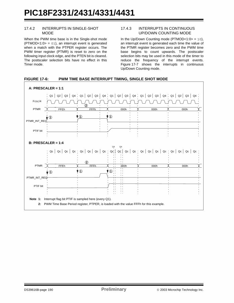
PIC18F2331/2431/4331/4431
17.4.2 INTERRUPTS IN SINGLE-SHOT MODE
When the PWM time base is in the Single-shot mode(PTMOD<1:0> = 01), an interrupt event is generatedwhen a match with the PTPER register occurs. ThePWM timer register (PTMR) is reset to zero on thefollowing input clock edge, and the PTEN bit is cleared.The postscaler selection bits have no effect in thisTimer mode.
17.4.3 INTERRUPTS IN CONTINUOUS UP/DOWN COUNTING MODE
In the Up/Down Counting mode (PTMOD<1:0> = 10),an interrupt event is generated each time the value ofthe PTMR register becomes zero and the PWM timebase begins to count upwards. The postscalerselection bits may be used in this mode of the timer toreduce the frequency of the interrupt events.Figure 17-7 shows the interrupts in continuousUp/Down Counting mode.
FIGURE 17-6: PWM TIME BASE INTERRUPT TIMING, SINGLE SHOT MODE
Q2Q1 Q3 Q4Q2Q1 Q3 Q4 Q2Q1 Q3 Q4 Q2Q1 Q3 Q4 Q2Q1 Q3 Q4
1 1
FOSC/4
PTMR FFEh FFFh 000h 000h 000h
1
PTIF bit
2
Note 1: Interrupt flag bit PTIF is sampled here (every Q1).
2: PWM Time Base Period register, PTPER, is loaded with the value FFFh for this example.
QcQc Qc QcQcQc Qc Qc QcQc Qc Qc QcQc Qc Qc QcQc Qc Qc
1 1
PTMR FFEh FFFh 000h 000h 000h
1
2
A: PRESCALER = 1:1
B: PRESCALER = 1:4
PTMR_INT_REQ
Q4Q4
PTIF bit
PTMR_INT_REQ
DS39616B-page 190 Preliminary 2003 Microchip Technology Inc.

PIC18F2331/2431/4331/4431
FIGURE 17-7: PWM TIME BASE INTERRUPTS, UP/DOWN COUNTING MODE
Q2Q1 Q3 Q4Q2Q1 Q3 Q4 Q2Q1 Q3 Q4 Q2Q1 Q3 Q4 Q2Q1 Q3 Q4
FOSC/4
PTMR 002h 001h 000h 001h 002h
Note 1: Interrupt flag bit PTIF is sampled here (every Q1).
QcQc Qc QcQcQc Qc Qc QcQc Qc Qc QcQc Qc Qc QcQc Qc Qc
1 1
PTMR 002h 001h 000h 001h 002h
1PTDIR bit
1
PRESCALER = 1:1
PRESCALER = 1:4
PTIF bit
PTMR_INT_REQ
PTDIR bit
Q4Q4
PTIF bit
PTMR_INT_REQ
1 1 1 1
2003 Microchip Technology Inc. Preliminary DS39616B-page 191

PIC18F2331/2431/4331/4431
17.4.4 INTERRUPTS IN DOUBLE UPDATE MODE
This mode is available in Up/Down Counting mode. Inthe Double Update mode (PTMOD<1:0> = 11), aninterrupt event is generated each time the PTMRregister is equal to zero and each time the PTMRmatches with PTPER register. Figure 17-8 shows theinterrupts in Up/Down Counting mode with doubleupdates.
The Double Update mode provides two additionalfunctions to the user in Center-Aligned mode.
1. The control loop bandwidth is doubled becausethe PWM duty cycles can be updated twice perperiod.
2. Asymmetrical center-aligned PWM waveformscan be generated, which are useful forminimizing output waveform distortion in certainmotor control applications.
FIGURE 17-8: PWM TIME BASE INTERRUPTS, UP/DOWN COUNTING MODE WITH DOUBLE UPDATES
Note: Do not change PTMOD while PTEN isactive. It will yield unexpected results. Tochange PWM Timer mode of operation,first clear PTEN bit, load PTMOD withrequired data and then set PTEN.
Q2Q1 Q3 Q4Q2Q1 Q3 Q4 Q2Q1 Q3 Q4 Q2Q1 Q3 Q4 Q2Q1 Q3 Q4
1 1
OSC1
PTMR 3FDh 3FEh 3FFh 3FEh 3FDh
1
Case 1: PTMR Counting Upwards
Q2Q1 Q3 Q4Q2Q1 Q3 Q4 Q2Q1 Q3 Q4 Q2Q1 Q3 Q4 Q2Q1 Q3 Q4
1 1
OSC1
PTMR 002h 001h 000h 001h 002h
1
Case 2: PTMR Counting Downwards
2
Note 1: Interrupt flag bit PTIF is sampled here (every Q1).
2: PWM Time Base Period register, PTPER, is loaded with the value 3FFh for this example.
1
1
PTIF bit
PTMR_INT_REQ
PTIF bit
PTMR_INT_REQ
A: PRESCALER = 1:1
PTDIR bit
PTDIR bit
DS39616B-page 192 Preliminary 2003 Microchip Technology Inc.

PIC18F2331/2431/4331/4431
17.5 PWM Period
The PWM period is defined by the PTPER register pair(PTPERL and PTPERH). The PWM period has 12-bitresolution by combining 4 LSBs of PTPERH and 8-bitsof PTPERL. PTPER is a double-buffered register usedto set the counting period for the PWM time base.
The PTPER buffer contents are loaded into the PTPERregister at the following times:
• Free Running and Single-shot modes: when the PTMR register is reset to zero after a match with the PTPER register.
• Up/Down Counting modes: When the PTMR register is zero. The value held in the PTPER buffer is automatically loaded into the PTPER register when the PWM time base is disabled (PTEN = 0). Figure 17-9 and Figure 17-10 indicate the times when the contents of the PTPER buffer are loaded into the actual PTPER register.
The PWM period can be calculated from the followingformulas:
EQUATION 17-1: PWM PERIOD FOR FREE RUNNING MODE
EQUATION 17-2: PWM PERIOD FOR UP/DOWN COUNTING MODE
The PWM frequency is the inverse of period; or
The maximum resolution (in bits) for a given deviceoscillator and PWM frequency can be determined fromthe following formula:
EQUATION 17-3: PWM RESOLUTION
The PWM resolutions and frequencies are shown for aselection of execution speeds and PTPER values inTable 17-2. The PWM frequencies in Table 17-2 arecalculated for Edge-aligned PWM mode. ForCenter-aligned mode, the PWM frequencies will beapproximately one-half the values indicated in thistable.
TABLE 17-2: EXAMPLE PWM FREQUENCIES AND RESOLUTIONS
TPWM = (PTPER + 1)
Fosc/(PTMRPS/4)
TPWM = (PTPER + 1) x PTMRPS
Fosc/4
or
TPWM = (2 x PTPER)
Fosc/(PTMRPS/4)
PWM frequency 1PWM period-------------------------------=
PWM Frequency = 1/TPWM
Fosc MIPSPTPER Value
PWM Resolution
PWM Frequency
40 MHz 10 0FFFh 14 bits 2.4 kHz 40 MHz 10 07FFh 13 bits 4.9 kHz 40 MHz 10 03FFh 12 bits 9.8 kHz
40 MHz 10 01FFh 11 bits 19.5 kHz40 MHz 10 FFh 10 bits 39.0 kHz40 MHz 10 7Fh 9 bits 78.1 kHz
40 MHz 10 3Fh 8 bits 156.2 kHz40 MHz 10 1Fh 7 bits 312.5 kHz40 MHz 10 0Fh 6 bits 625 kHz
25 MHz 6.25 0FFFh 14 bits 1.5 kHz25 MHz 6.25 03FFh 12 bits 6.1 kHz25 MHz 6.25 FFh 10 bits 24.4 kHz
10 MHz 2.5 0FFFh 14 bits 610 Hz10 MHz 2.5 03FFh 12 bits 2.4 kHz10 MHz 2.5 FFh 10 bits 9.8 kHz
5 MHz 1.25 0FFFh 14 bits 305 Hz5 MHz 1.25 03FFh 12 bits 1.2 kHz5 MHz 1.25 FFh 10 bits 4.9 kHz
4 MHz 1 0FFFh 14 bits 244 Hz4 MHz 1 03FFh 12 bits 976 Hz4 MHz 1 FFh 10 bits 3.9 kHz
Note: For center-aligned operation, PWM frequencies will be approximately 1/2 the value indicated in the table.
Resolution = log(2)
logFosc/4Fpwm
2003 Microchip Technology Inc. Preliminary DS39616B-page 193

PIC18F2331/2431/4331/4431
FIGURE 17-9: PWM PERIOD BUFFER UPDATES IN FREE RUNNING COUNT MODE
FIGURE 17-10: PWM PERIOD BUFFER UPDATES IN UP/DOWN COUNTING MODES
Old PTPER value = 004
New PTPER value = 007
Period value loaded from PTPER Buffer register
New value written to PTPER buffer.
01
23
4
01
23
4
01
23
4
5
67
Old PTPER value = 004
New PTPER value = 007
Period value loaded from
PTPER Buffer register
New value written to PTPER buffer.
01
2
3
4
3
2
1
01
2
3
4
5
6
7
3
2
1
0
4
5
6
DS39616B-page 194 Preliminary 2003 Microchip Technology Inc.

PIC18F2331/2431/4331/4431
17.6 PWM Duty Cycle
PWM duty cycle is defined by PDCx (PDCxL andPDCxH) registers. There are a total of 4 PWM DutyCycle registers for 4 pairs of PWM channels. The DutyCycle registers have 14-bit resolution by combining6 LSbs of PDCxH with the 8 bits of PDCxL. PDCx is adouble-buffered register used to set the countingperiod for the PWM time base.
17.6.1 PWM DUTY CYCLE REGISTERS
There are four 14-bit special function registers used tospecify duty cycle values for the PWM module:
• PDC0 (PDC0L and PDC0H)• PDC1 (PDC1L and PDC1H)
• PDC2 (PDC2L and PDC2H)• PDC3 (PDC3L and PDC3H)
The value in each Duty Cycle register determines theamount of time that the PWM output is in the activestate. The upper 12 bits of PDCn hold the actual dutycycle value from PTMRH/L<11:0>, while the lower 2bits control which internal Q-clock the duty cycle matchoccurs. This 2-bit value is decoded from the Q-clocksas shown in Figure 17-11 (when the prescaler is 1:1(PTCKPS = 00)).
In Edge-aligned mode, the PWM period starts at Q1and ends when the Duty Cycle register matches thePTMR register as follows. The duty cycle match is con-sidered when the upper 12 bits of the PDC is equal tothe PTMR and the lower 2 bits are equal to Q1, Q2, Q3or Q4, depending on the lower two bits of the PDC(when the prescaler is 1:1, or PTCKPS = 00).
Each compare unit has logic that allows override of thePWM signals. This logic also ensures that the PWMsignals will complement each other (with dead timeinsertion) in Complementary mode (see Section 17.7“Dead Time Generators”).
FIGURE 17-11: DUTY CYCLE COMPARISON
Note: When prescaler is not 1:1 (PTCKPS ≠~00), the duty cycle match occurs at Q1clock of the instruction cycle when thePTMR and PDC match occurs.
PTMR<11:0>
PDCn<13:0>
COMPARATOR
UNUSED
UNUSED
PTMRH<7:0> PTMRL<7:0>
PTMRH<3:0> PTMRL<7:0> Q-CLOCKS(1)
PDCnH<7:0> PDCnL<7:0>
PDCnH<5:0> PDCnL<7:0>
<1:0>
Note 1: This value is decoded from the Q-Clocks: 00 = duty cycle match occurs on Q1 01 = duty cycle match occurs on Q2 10 = duty cycle match occurs on Q3 11 = duty cycle match occurs on Q4
2003 Microchip Technology Inc. Preliminary DS39616B-page 195

PIC18F2331/2431/4331/4431
17.6.2 DUTY CYCLE REGISTER BUFFERS
The four PWM Duty Cycle registers aredouble-buffered to allow glitchless updates of the PWMoutputs. For each duty cycle block, there is a DutyCycle Buffer register that is accessible by the user anda second Duty Cycle register that holds the actualcompare value used in the present PWM period.
In edge-aligned PWM Output mode, a new duty cyclevalue will be updated whenever a PTMR match with thePTPER register occurs and PTMR is reset as shown inFigure 17-12. Also, the contents of the duty cyclebuffers are automatically loaded into the Duty Cycleregisters when the PWM time base is disabled (PTEN = 0).
When the PWM time base is in the Up/Down Countingmode, new duty cycle values will be updated when thevalue of the PTMR register is zero and the PWM timebase begins to count upwards. The contents of the dutycycle buffers are automatically loaded into the DutyCycle registers when the PWM time base is disabled(PTEN = 0). Figure 17-13 shows the timings when theduty cycle update occur for the Up/Down Count mode.In this mode, up to one entire PWM period is availablefor calculating and loading the new PWM duty cyclebefore changes take effect.
When the PWM time base is in the Up/Down Countingmode with double updates, new duty cycle values willbe updated when the value of the PTMR register is zeroand when the value of the PTMR register matches thevalue in the PTPER register. The contents of the dutycycle buffers are automatically loaded into the DutyCycle registers during both of the above saidconditions. Figure 17-14 shows the duty cycle updatesfor Up/Down mode with double update. In this mode,only up to half of a PWM period is available forcalculating and loading the new PWM duty cycle beforechanges take effect.
17.6.3 EDGE-ALIGNED PWM
Edge-aligned PWM signals are produced by themodule when the PWM time base is in the FreeRunning mode or the Single-shot mode. Foredge-aligned PWM outputs, the output for a givenPWM channel has a period specified by the valueloaded in PTPER and a duty cycle specified by theappropriate Duty Cycle register (see Figure 17-12).The PWM output is driven active at the beginning of theperiod (PTMR = 0) and is driven inactive when thevalue in the Duty Cycle register matches PTMR. A newcycle is started when PTMR matches the PTPER asexplained in the PWM period section.
If the value in a particular Duty Cycle register is zero,then the output on the corresponding PWM pin will beinactive for the entire PWM period. In addition, the out-put on the PWM pin will be active for the entire PWMperiod if the value in the Duty Cycle register is greaterthan the value held in the PTPER register.
FIGURE 17-12: EDGE-ALIGNED PWM
FIGURE 17-13: DUTY CYCLE UPDATE TIMES IN UP/DOWN COUNTING MODE
Period
Duty Cycle
0
PTPER
PTMRValue
New Duty Cycle Latched
Active at
of periodbeginning
PDC
PDC(new)
(old)
PTMR Value
PWM output
Duty cycle value loaded from buffer register
New value written to duty cycle buffer
DS39616B-page 196 Preliminary 2003 Microchip Technology Inc.

PIC18F2331/2431/4331/4431
FIGURE 17-14: DUTY CYCLE UPDATE TIMES IN UP/DOWN COUNTING MODE WITH DOUBLE UPDATES
17.6.4 CENTER-ALIGNED PWM
Center-aligned PWM signals are produced by themodule when the PWM time base is configured in anUp/Down Counting mode (see Figure 17-15). ThePWM compare output is driven to the active state whenthe value of the Duty Cycle register matches the valueof PTMR and the PWM time base is countingdownwards (PTDIR = 1). The PWM compare outputwill be driven to the inactive state when the PWM timebase is counting upwards (PTDIR = 0) and the value inthe PTMR register matches the duty cycle value. If thevalue in a particular Duty Cycle register is zero, thenthe output on the corresponding PWM pin will be
inactive for the entire PWM period. In addition, theoutput on the PWM pin will be active for the entire PWMperiod if the value in the Duty Cycle register is equal toor greater than the value in the PTPER register.
FIGURE 17-15: START OF CENTER-ALIGNED PWM
PTMR Value
PWM output
Duty cycle value loaded from buffer register
New values written to duty cycle buffer.
Note: When the PWM is started inCenter-aligned mode, the period register(PTPER) is loaded into the PWM Timerregister (PTMR) and the PTMR isconfigured automatically to startdown-counting. This is done to ensure thatall the PWM signals don’t start at the sametime.
0
PTPER
PTMRValue
Period
Period/2
DutyCycle
Start of
first
PWMPeriod
Period
Duty Cycle
2003 Microchip Technology Inc. Preliminary DS39616B-page 197

PIC18F2331/2431/4331/4431
17.6.5 COMPLEMENTARY PWM OPERATION
The Complementary mode of PWM operation is usefulto drive one or more power switches in half-bridgeconfiguration as shown in Figure 17-16. This invertertopology is typical for a 3-phase induction motor,brushless DC motor or a 3-phase UninterruptiblePower Supply (UPS) control applications. Eachupper/lower power switch pair is fed by acomplementary PWM signal. Dead time may beoptionally inserted during device switching where bothoutputs are inactive for a short period (seeSection 17.7 “Dead Time Generators”). InComplementary mode, the duty cycle comparison unitsare assigned to the PWM outputs as follows:
• PDC0 register controls PWM1/PWM0 outputs
• PDC1 register controls PWM3/PWM2 outputs• PDC2 register controls PWM5/PWM4 outputs• PDC3 register controls PWM7/PWM6 outputs
PWM1/3/5/7 are the main PWMs that are controlled bythe PDC registers and PWM0/2/4/6 are thecomplemented outputs. When using the PWMs tocontrol the half bridge, the odd number PWMs can beused to control the upper power switch and the evennumbered PWMs for the lower switches.
FIGURE 17-16: TYPICAL LOAD FOR COMPLEMENTARY PWM OUTPUTS
The Complementary mode is selected for each PWMI/O pin pair by clearing the appropriate PMODx bit inthe PWMCON0 register. The PWM I/O pins are set toComplementary mode by default upon all kinds ofdevice resets.
+V
PW
M1
PW
M0
PW
M3
PW
M2
PW
M5
PW
M4
3 Phase
Load
DS39616B-page 198 Preliminary 2003 Microchip Technology Inc.

PIC18F2331/2431/4331/4431
17.7 Dead Time Generators
In power inverter applications where the PWMs areused in Complementary mode to control the upper andlower switches of a half-bridge, a dead time insertion ishighly recommended. The dead time insertion keepsboth outputs in inactive state for a brief time. Thisavoids any overlap in the switching during the statechange of the power devices due to TON and TOFF
characteristics.
Because the power output devices cannot switchinstantaneously, some amount of time must be pro-vided between the turn-off event of one PWM output ina complementary pair and the turn-on event of theother transistor. The PWM module allows dead time tobe programmed. Following sections explain the deadtime block in detail.
17.7.1 DEAD TIME INSERTION
Each complementary output pair for the PWM modulehas a 6-bit down counter used to produce the deadtime insertion. As shown in Figure 17-17, each deadtime unit has a rising and falling edge detector con-nected to the duty cycle comparison output. The deadtime is loaded into the timer on the detected PWM edgeevent. Depending on whether the edge is rising or fall-ing, one of the transitions on the complementary out-puts is delayed until the timer counts down to zero. Atiming diagram indicating the dead time insertion forone pair of PWM outputs is shown in Figure 17-18.
FIGURE 17-17: DEAD TIME CONTROL UNIT BLOCK DIAGRAM FOR ONE PWM OUTPUT PAIR
FIGURE 17-18: DEAD TIME INSERTION FOR COMPLEMENTARY PWM
Even PWM Signal ToOutput Control Block
Odd PWM Signal ToOutput Control Block
Zero Compare
Clock Control and Prescaler
6-Bit Down Counter
Duty CycleCompare Input
Dead TimePrescale
FOSC
Dead TimeSelect Bits
Dead Time Register
td
PDC1compareoutput
PWM1
PWM0
td
2003 Microchip Technology Inc. Preliminary DS39616B-page 199

PIC18F2331/2431/4331/4431
REGISTER 17-5: DTCON – DEAD TIME CONTROL REGISTER
17.7.2 DEAD TIME RANGES
The amount of dead time provided by the dead timeunit is selected by specifying the input clock prescalervalue and a 6-bit unsigned value defined in the DTCONregister. Four input clock prescaler selections havebeen provided to allow a suitable range of dead timesbased on the device operating frequency. FOSC/2,FOSC/4, FOSC/8 and FOSC/16 are the clock prescaleroptions available using the DTPS1:DTPS0 control bitsin the DTCON register.
After selecting an appropriate prescaler value, thedead time is adjusted by loading a 6-bit unsigned valueinto DTCON<5:0>. The dead time unit prescaler iscleared on any of the following events:
• On a load of the down timer due to a duty cycle comparison edge event;
• On a write to the DTCON register; or• On any device Reset.
17.7.3 DECREMENTING THE DEAD TIME COUNTER
The dead time counter is clocked from any of the Qclocks based on the following conditions.
1. The dead time counter is clocked on Q1 when: • The DTPS bits are set to any of the following
dead time prescaler settings: Fosc/4, FOSC/8, FOSC/16
• The PWM Time Base Prescale bits (PTCKPS) are set to any of the following prescale ratios: FOSC/16, FOSC/64, FOSC/256.
2. The dead time counter is clocked by a pair ofQ-clocks when the PWM Time Base Prescalebits are set to 1:1 (PTCKPS1:PTCKPS0 = 00,FOSC/4) and the dead time counter is clocked bythe FOSC/2 (DTPS1:DTPS0 = 00).
3. The dead time counter is clocked using everyother Q-clock depending on the two LSbs in theDuty Cycle registers:• If the PWM duty cycle match occurs on Q1 or
Q3, then the dead time counter is clocked using every Q1 and Q3.
• If the PWM duty cycles match occurs on Q2 or Q4, then the dead time counter is clocked using every Q2 and Q4.
4. When the DTPS1:DTPS0 bits are set to any ofthe other dead time prescaler settings, (i.e.,FOSC/4, FOSC/8 or FOSC/16) and the PWM TimeBase Prescaler is set to 1:1, the dead timecounter is clocked by the Q-clock correspondingto the Q-clocks on which the PWM duty cyclematch occurs.
The actual dead time is calculated from the DTCONregister as follows:
Dead Time = Dead time value / (FOSC/prescaler)
Table 17-3 shows example dead time ranges as afunction of the input clock prescaler selected and thedevice operating frequency.
R/W-0 R/W-0 R/W-0 R/W-0 R/W-0 R/W-0 R/W-0 R/W-0DTPS1 DTPS0 DT5 DT4 DT3 DT2 DT1 DT0
bit 7 bit 0
bit 7-6 DTPS1:DTPS0: Dead Time Unit A Prescale Select bits11 = Clock source for Dead Time Unit is FOSC/16.10 = Clock source for Dead Time Unit is FOSC/8.01 = Clock source for Dead Time Unit is FOSC/4.00 = Clock source for Dead Time Unit is FOSC/2.
bit 5-0 DT5:DT0: Unsigned 6-bit dead time value bits for Dead Time Unit.
Legend:
R = Readable bit W = Writable bit U = Unimplemented bit, read as ‘0’
-n = Value at POR ‘1’ = bit is set ‘0’ = bit is cleared x = bit is unknown
DS39616B-page 200 Preliminary 2003 Microchip Technology Inc.

PIC18F2331/2431/4331/4431
TABLE 17-3: EXAMPLE DEAD TIME RANGES
17.7.4 DEAD TIME DISTORTION
17.8 Independent PWM Output
Independent PWM mode is used for driving the loadsas shown in Figure 17-19 for driving one winding of aswitched reluctance motor. A particular PWM outputpair is configured in the Independent Output modewhen the corresponding PMOD bit in the PWMCON0register is set. No dead time control is implementedbetween the PWM I/O pins when the module is operat-ing in the Independent mode and both I/O pins areallowed to be active simultaneously. This mode canalso be used to drive stepper motors.
17.8.1 DUTY CYCLE ASSIGNMENT IN THE INDEPENDENT MODE
In the Independent mode, each duty cycle generator isconnected to both PWM output pins in a given PWMoutput pair. The odd and the even PWM output pins aredriven with a single PWM duty cycle generator. PWM1and PWM0 are driven by the PWM channel which usesPDC0 register to set the duty cycle, PWM3 and PWM2with PDC1, PWM5 and PWM4 with PDC2, PWM7 andPWM6 with PDC3, see Figure 17-3 and Register 17-3.
Fosc(MHz)
MIPSPrescaler Selection
Dead Time Min
Dead Time Max
40 10 FOSC/2 50 ns 3.2 µs
40 10 FOSC/4 100 ns 6.4 µs40 10 FOSC/8 200 ns 12.8 µs40 10 FOSC/16 400 ns 25.6 µs
32 8 FOSC/2 62.5 ns 4 µs32 8 FOSC/4 125 ns 8 µs32 8 FOSC/8 250 ns 16 µs
32 8 FOSC/16 500 ns 32 µs25 6.25 FOSC/2 80 ns 5.12 vs25 6.25 FOSC/4 160 ns 10.2 µs
25 6.25 FOSC/8 320 ns 20.5 µs25 6.25 FOSC/16 640 ns 41 µs20 5 FOSC/2 100 ns 6.4 µs
20 5 FOSC/4 200 ns 12.8 µs20 5 FOSC/8 400 25.6 vs20 5 FOSC/16 800 51.2 µs
10 2.5 FOSC/2 200 ns 12.8 µs10 2.5 FOSC/4 400 ns 25.6 µs10 2.5 FOSC/8 800 ns 51.2 µs
10 2.5 FOSC/16 1.6 µs 102.4 µs5 1.25 FOSC/2 400 ns 25.6 µs5 1.25 FOSC/4 800 ns 51.2 µs
5 1.25 FOSC/8 1.6 µs 102.4 µs5 1.25 FOSC/16 3.2 µs 204.8 µs4 1 FOSC/2 0.5 µs 32 µs
4 1 FOSC/4 1 µs 64 µs4 1 FOSC/8 2 µs 128 µs4 1 FOSC/16 4 µs 256 µs
Note 1: For small PWM duty cycles, the ratio ofdead time to the active PWM time maybecome large. In this case, the inserteddead time will introduce distortion intowaveforms produced by the PWM mod-ule. The user can ensure that dead timedistortion is minimized by keeping thePWM duty cycle at least three timeslarger than the dead time. A similar effectoccurs for duty cycles at or near 100%.The maximum duty cycle used in theapplication should be chosen such thatthe minimum inactive time of the signal isat least three times larger than the deadtime. If the dead time is greater or equalto the duty cycle of one of the PWM out-puts pairs, then that PWM pair will beinactive for the whole period.
2: Changing the dead time values inDTCON when the PWM is enabled mayresult in undesired situation. Disable thePWM (PTEN = 0) before changing thedead time value
2003 Microchip Technology Inc. Preliminary DS39616B-page 201

PIC18F2331/2431/4331/4431
17.8.2 PWM CHANNEL OVERRIDE
PWM output may be manually overridden for eachPWM channel by using the appropriate bits in theOVDCOND and OVDCONS registers. The user mayselect the following signal output options for each PWMoutput pin operating in the Independent mode:
• I/O pin outputs PWM signal• I/O pin inactive
• I/O pin active
Refer to Section 17.10 “PWM Output Override” fordetails for all the override functions.
FIGURE 17-19: CENTER-CONNECTED LOAD
17.9 Single-Pulse PWM Operation
The single pulse PWM operation is available only inEdge-aligned mode. In this mode, the PWM module willproduce single pulse output. Single-pulse operation isconfigured when the PTMOD1:PTMOD0 bits are set to‘01’ in PTCON0 register. This mode of operation is use-ful for driving certain types of ECMs.
In Single-pulse mode, the PWM I/O pin(s) are driven tothe active state when the PTEN bit is set. When thePWM timer match with Duty Cycle register occurs, thePWM I/O pin is driven to the inactive state. When thePWM timer match with the PTPER register occurs, thePTMR register is cleared, all active PWM I/O pins aredriven to the inactive state, the PTEN bit is cleared, andan interrupt is generated, if the corresponding interruptbit is set.
17.10 PWM Output Override
The PWM output override bits allow the user to manu-ally drive the PWM I/O pins to specified logic statesindependent of the duty cycle comparison units. ThePWM override bits are useful when controlling varioustypes of ECMs like a BLDC motor.
OVDCOND and OVDCONS registers are used todefine the PWM override options. The OVDCONDregister contains eight bits, POVD7:POVD0, thatdetermine which PWM I/O pins will be overridden. TheOVDCONS register contains eight bits,POUT7:POUT0, that determine the state of the PWMI/O pins when a particular output is overridden via thePOVD bits.
The POVD bits are active-low control bits. When thePOVD bits are set, the corresponding POUT bit willhave no effect on the PWM output. In other words, thepins corresponding to POVD bits that are set will havethe duty PWM cycle set by the PDC registers. Whenone of the POVD bits is cleared, the output on the cor-responding PWM I/O pin will be determined by thestate of the POUT bit. When a POUT bit is set, thePWM pin will be driven to its active state. When thePOUT bit is cleared, the PWM pin will be driven to itsinactive state.
17.10.1 COMPLEMENTARY OUTPUT MODE
The even-numbered PWM I/O pin has override restric-tions when a pair of PWM I/O pins are operating in theComplementary mode (PMODx = 0). In Complemen-tary mode, if the even-numbered pin is driven active byclearing the corresponding POVD bit and by settingPOUT bits in OVDCOND and OVDCONS registers, theoutput signal is forced to be the complement of theodd-numbered I/O pin in the pair (see Figure 17-2 fordetails).
17.10.2 OVERRIDE SYNCHRONIZATION
If the OSYNC bit in the PWMCON1 register is set, alloutput overrides performed via the OVDCOND andOVDCONS registers will be synchronized to the PWMtime base. Synchronous output overrides will occur onfollowing conditions:
• When the PWM is in Edge-aligned mode, syn-chronization occurs when PTMR is zero.
• When the PWM is in Center-aligned mode, synchronization occurs when PTMR is zero and when the value of PTMR matches PTPER.
Note: PTPER and PDC values are held as it isafter the single pulse output. To haveanother cycle of single pulse, only PTENhas to be enabled.
+V
PWM1
PWM0
LOAD
Note 1: In the Complementary mode, the evenchannel cannot be forced active by a faultor override event when the odd channel isactive. The even channel is always thecomplement of the odd channel with deadtime inserted, before the odd channel canbe driven to its active state as shown inFigure 17-20.
2: Dead time inserted to the PWM channelseven when they are in Override mode.
DS39616B-page 202 Preliminary 2003 Microchip Technology Inc.

PIC18F2331/2431/4331/4431
FIGURE 17-20: OVERRIDE BITS IN COMPLEMENTARY MODE
17.10.3 OUTPUT OVERRIDE EXAMPLES
Figure 17-21 shows an example of a waveform thatmight be generated using the PWM output overridefeature. The figure shows a six-step commutationsequence for a BLDC motor. The motor is driventhrough a 3-phase inverter as shown in Figure 17-16.When the appropriate rotor position is detected, thePWM outputs are switched to the next commutationstate in the sequence. In this example, the PWM out-puts are driven to specific logic states. The OVDCONDand OVDCONS register values used to generate thesignals in Figure 17-21 are given in Table 17-4.
The PWM Duty Cycle registers may be used in con-junction with the OVDCOND and OVDCONS registers.The Duty Cycle registers control the average voltageacross the load and the OVDCOND and OVDCONSregisters control the commutation sequence.Figure 17-22 shows the waveforms, while Table 17-4and Table 17-5 show the OVDCOND and OVDCONSregister values used to generate the signals.
REGISTER 17-6: OVDCOND: OUTPUT OVERRIDE CONTROL REGISTER
1. Even override bits have no effect in Complementary mode.2. Odd override bit is activated, which causes the even PWM to deactivate.3. Dead time insertion.
4. Odd PWM activated after the dead time.5. Odd override bit is deactivated, which causes the odd PWM to deactivate.6. Dead time insertion.
7. Even PWM is activated after the dead time.
POUT0
POUT1
PWM1
PWM0
Assume: PVOD0 = 0; PVOD1 = 0; PMOD0 = 0
6
54
3
2 7
1
R/W-1 R/W-1 R/W-1 R/W-1 R/W-1 R/W-1 R/W-1 R/W-1POVD7(1) POVD6(1) POVD5 POVD4 POVD3 POVD2 POVD1 POVD0
bit 7 bit 0
bit 7-0 POVD7:POVD0: PWM Output Override bits(1)
1 = Output on PWM I/O pin is controlled by the value in the Duty Cycle register and the PWMtime base.
0 = Output on PWM I/O pin is controlled by the value in the corresponding POUT bit.
Note 1: Unimplemented in PIC18F2X31 devices; maintain these bits clear.
Legend:
R = Readable bit W = Writable bit U = Unimplemented bit, read as ‘0’
-n = Value at POR ‘1’ = bit is set ‘0’ = bit is cleared x = bit is unknown
2003 Microchip Technology Inc. Preliminary DS39616B-page 203

PIC18F2331/2431/4331/4431
REGISTER 17-7: OVDCONS: OUTPUT STATE REGISTER
FIGURE 17-21: PWM OUTPUT OVERRIDE EXAMPLE #1
TABLE 17-4: PWM OUTPUT OVERRIDE EXAMPLE #1
TABLE 17-5: PWM OUTPUT OVERRIDE EXAMPLE #2
FIGURE 17-22: PWM OUTPUT OVERRIDE EXAMPLE #2
R/W-0 R/W-0 R/W-0 R/W-0 R/W-0 R/W-0 R/W-0 R/W-0POUT7(1) POUT6(1) POUT5 POUT4 POUT3 POUT2 POUT1 POUT0
bit 7 bit 0
bit 7-0 POUT7:POUT0: PWM Manual Output bits(1)
1 = Output on PWM I/O pin is ACTIVE when the corresponding PWM output override bit iscleared.
0 = Output on PWM I/O pin is INACTIVE when the corresponding PWM output override bit iscleared.
Note 1: Unimplemented in PIC18F2X31 devices; maintain these bits clear.
Legend:
R = Readable bit W = Writable bit U = Unimplemented bit, read as ‘0’
-n = Value at POR ‘1’ = bit is set ‘0’ = bit is cleared x = bit is unknown
State OVDCOND(POVD) OVDCONS(POUT)
1 00000000b 00100100b
2 00000000b 00100001b
3 00000000b 00001001b
4 00000000b 00011000b
5 00000000b 00010010b
6 00000000b 00000110b
State OVDCOND (POVD) OVDCONS (POUT)
1 11000011b 00000000b
2 11110000b 00000000b
3 00111100b 00000000b
4 00001111b 00000000b
PWM5
PWM4
PWM3
PWM2
PWM1
PWM0
1 2 3 4 5 6
PWM7
PWM6
PWM5
PWM4
PWM3
PWM2
1 2 3 4
PWM1
PWM0
DS39616B-page 204 Preliminary 2003 Microchip Technology Inc.

PIC18F2331/2431/4331/4431
17.11 PWM Output and Polarity Control
There are three device configuration bits associatedwith the PWM module that provide PWM output pincontrol defined in CONFIG3L configuration register.
• HPOL configuration bit• LPOL configuration bit• PWMPIN configuration bit
These three configuration bits work in conjunction withthe three PWM enable bits (PWMEN2:PWMEN0) in thePWMCON0 register. The configuration bits and PWMenable bits ensure that the PWM pins are in the correctstates after a device Reset occurs.
17.11.1 OUTPUT PIN CONTROL
The PWMEN2:PWMEN0 control bits enable eachPWM output pin as required in the application.
All PWM I/O pins are general purpose I/O. When a pairof pins are enabled for PWM output, the PORT andTRIS registers controlling the pin are disabled. Refer toFigure 17-23 for details.
FIGURE 17-23: PWM I/O PIN BLOCK DIAGRAM
17.11.2 OUTPUT POLARITY CONTROL
The polarity of the PWM I/O pins is set during deviceprogramming via the HPOL and LPOL configurationbits in the CONFIG3L device configuration register.The HPOL configuration bit sets the output polarity forthe high-side PWM outputs, PWM1, PWM3, PWM5and PWM7. The polarity is active-high when HPOL iscleared (= 0), and active-low when it is set (= 1).
The LPOL configuration bit sets the output polarity forthe low-side PWM outputs, PWM0, PWM2, PWM4 andPWM6. As with HPOL, they are active-high when LPOLis cleared, and active-low when set.
All output signals generated by the PWM module arereferenced to the polarity control bits, including thosegenerated by fault inputs or manual override (seeSection 17.10 “PWM Output Override”).
The default polarity configuration bits have the PWMI/O pins in active-high output polarity.
Data Bus
WR PORT
WR TRIS
RD PORT
Data Latch
TRIS Latch
P
VSS
I/O Pin
QD
QCK
QD
QCK
Q D
EN
N
VDD
RD TRIS SchmittTrigger
TTL or
0
1
PWM Pin Enable
PWM signal frommodule
Note: I/O pin has protection diodes to VDD and VSS. PWM polarity selection logic not shown for clarity.
2003 Microchip Technology Inc. Preliminary DS39616B-page 205

PIC18F2331/2431/4331/4431
17.11.3 PWM OUTPUT PIN RESET STATES
The PWMPIN configuration bit determines the PWMoutput pins to be PWM output pins or digital I/O pins,after the device comes out of reset. If the PWMPIN con-figuration bit is unprogrammed (default), thePWMEN2:PWMEN0 control bits will be cleared on adevice Reset. Consequently, all PWM outputs will betri-stated and controlled by the corresponding PORTand TRIS registers. If the PWMPIN configuration bit isprogrammed low, the PWMEN2:PWMEN0 control bitswill be set as follows on a device Reset:
• PWMEN2:PWMEN0 = 101 if device has 8 PWM pins (PIC18F4X31 devices)
• PWMEN2:PWMEN0 = 100 if device has 6 PWM pins (PIC18F2X31 devices)
All PWM pins will be enabled for PWM output and willhave the output polarity defined by the HPOL andLPOL configuration bits.
17.12 PWM Fault Inputs
There are two fault inputs associated with the PWMmodule. The main purpose of the input fault pins is todisable the PWM output signals and drive them into aninactive state. The action of the fault inputs isperformed directly in hardware so that when a faultoccurs, it can be managed quickly and the PWMsoutputs are put into an inactive state to save the powerdevices connected to the PWMs.
The PWM fault inputs are FLTA and FLTB, which cancome from I/O pins, the CPU or another module. TheFLTA and FLTB pins are active-low inputs so it is easyto “OR” many sources to the same input.
The FLTCONFIG register (Register 17-8) defines thesettings of FLTA and FLTB inputs.
17.12.1 FAULT PIN ENABLE BITS
By setting the bits FLTAEN and FLTBEN in theFLTCONFIG register, the corresponding fault inputsare enabled. If both bits are cleared, then the faultinputs have no effect on the PWM module.
17.12.2 MFAULT INPUT MODES
The FLTAMOD and FLTBMOD bits in the FLTCONFIGregister determine the modes of PWM I/O pins that aredeactivated when they are overridden by fault input.
FLTAS and FLTBS bits in the FLTCONFIG register givethe status of FaultA and FaultB inputs.
Each of the fault inputs have two modes of operation:
• Inactive Mode (FLTxMOD = 0)
This is a catastrophic Fault Management mode.When the fault occurs in this mode, the PWM out-puts are deactivated. The PWM pins will remain inInactivated mode until the fault is cleared (faultinput is driven high) and the corresponding faultstatus bit has been cleared in software. The PWMoutputs are enabled immediately at the beginningof the following PWM period, after Fault Status bit(FLTxS) is cleared.
• Cycle-by-Cycle Mode (FLTxMOD = 1)
When the fault occurs in this mode, the PWM out-puts are deactivated. The PWM outputs willremain in the defined fault states (all PWM outputsinactive) for as long as the fault pin is held low.After the fault pin is driven high, the PWM outputswill return to normal operation at the beginning ofthe following PWM period, and the FLTS bit isautomatically cleared.
Note: The inactive state of the PWM pins aredependent on the HPOL and LPOL config-uration bit settings, which defines theactive and inactive state for PWM outputs.
DS39616B-page 206 Preliminary 2003 Microchip Technology Inc.

PIC18F2331/2431/4331/4431
17.12.3 PWM OUTPUTS WHILE IN FAULT CONDITION
While in the fault state (i.e., one or both FLTA and FLTBinputs are active), the PWM output signals are driveninto their inactive states. The selection of which PWMoutputs are deactivated (while in the fault state) isdetermined by the FLTCON bit in the FLTCONFIGregister as follows:
• FLTCON = 1. When FLTA or FLTB is asserted, the PWM outputs (i.e., PWM[7:0]) are driven into their inactive state
• FLTCON = 0. When FLTA or FLTB is asserted, only PWM[5:0] outputs are driven inactive, leaving PWM[7:6] activated.
17.12.4 PWM OUTPUTS IN DEBUG MODE
The BRFEN bit in the FLTCONFIG register controls thesimulation of fault condition when a breakpoint is hit,while debugging the application using a In-CircuitEmulator (ICE) or a In-Circuit Debugger (ICD). Settingthe BRFEN to high, enables the fault condition onbreakpoint, thus driving the PWM outputs to inactivestate. This is done to avoid any continuous keeping ofstatus on the PWM pin, which may result in damage ofthe power devices connected to the PWM outputs.
If BRFEN = 0, the fault condition on breakpoint isdisabled.
Note: Disabling only three PWM channels andleaving one PWM channel enabled whenin the fault state, allows the flexibility tohave at least one PWM channel enabled.None of the PWM outputs can be enabled(driven with the PWM Duty Cycle regis-ters) while FLTCON = 1 and the fault con-dition is present.
Note: It is highly recommended to enable thefault condition on breakpoint if a debug-ging tool is used, while developing thefirmware and the high-power circuitry isused. When the device is ready to pro-gram after debugging the firmware,BRFEN bit can be disabled.
2003 Microchip Technology Inc. Preliminary DS39616B-page 207

PIC18F2331/2431/4331/4431
REGISTER 17-8: FLTCONFIG: FAULT CONFIGURATION REGISTER R/W-0 R/W-0 R/W-0 R/W-0 R/W-0 R/W-0 R/W-0 R/W-0
BRFEN FLTBS(1) FLTBMOD(1) FLTBEN(1) FLTCON FLTAS FLTAMOD FLTAEN
bit 7 bit 0
bit 7 BRFEN: Breakpoint Fault Enable bit1 = Enable fault condition on a breakpoint (i.e., only when HDMIN = 1)0 = Disable fault condition
bit 6 FLTBS: Fault B Status bit(1)
1 = FLTB is asserted; if FLTBMOD = 0, cleared by the user if FLTBMOD = 1, cleared automatically at beginning of the new period when FLTB isdeasserted
0 = No Fault
bit 5 FLTBMOD: Fault B Mode bit(1)
1 = Cycle-by-cycle mode: Pins are inactive for the remainder of the current PWM period, or untilFLTB is deasserted. FLTBS is cleared automatically when FLTB is inactive (no fault present).
0 = Inactive mode: Pins are deactivated (catastrophic failure) until FLTB is deasserted andFLTBS is cleared by the user only.
bit 4 FLTBEN: Fault B Enable bit(1)
1 = Enable Fault B0 = Disable Fault B
bit 3 FLTCON: Fault Configuration bit1 = FLTA , FLTB or both deactivates all PWM outputs0 = FLTA or FLTB deactivates PWM[5:0]
bit 2 FLTAS: Fault A Status bit1 = FLTA is asserted;
If FLTAMOD = 0, cleared by the user If FLTAMOD = 1, cleared automatically at beginning of the new period when FLTA isdeasserted.
0 = No Fault
bit 1 FLTAMOD: Fault A Mode bit
1 = Cycle-by-cycle mode: Pins are inactive for the remainder of the current PWM period, or untilFLTA is deasserted. FLTAS is cleared automatically.
0 = Inactive mode: Pins are deactivated (catastrophic failure) until FLTA is deasserted andFLTAS is cleared by the user only.
bit 0 FLTAEN: Fault A Enable bit
1 = Enable Fault A0 = Disable Fault A
Note 1: Unimplemented in PIC18F2X31 devices; maintain these bits clear.
Legend:
R = Readable bit W = Writable bit U = Unimplemented bit, read as ‘0’
-n = Value at POR ‘1’ = bit is set ‘0’ = bit is cleared x = bit is unknown
DS39616B-page 208 Preliminary 2003 Microchip Technology Inc.

PIC18F2331/2431/4331/4431
17.13 PWM Update Lockout
For a complex PWM application, the user may need towrite up to four Duty Cycle registers and the Time BasePeriod Register, PTPER, at a given time. In someapplications, it is important that all buffer registers bewritten before the new duty cycle and period values areloaded for use by the module.
A PWM update lockout feature may optionally beenabled so the user may specify when new duty cyclebuffer values are valid. The PWM update lockoutfeature is enabled by setting the control bit UDIS in thePWMCON1 register. This bit affects all Duty CycleBuffer registers and the PWM time base period buffer,PTPER.
To perform a PWM update lockout:
1. Set the UDIS bit.2. Write all Duty Cycle registers and PTPER, if
applicable.3. Clear the UDIS bit to re-enable updates.4. With this, when UDIS bit is cleared, the buffer
values will be loaded to the actual registers. Thismakes a synchronous loading of the registers.
17.14 PWM Special Event Trigger
The PWM module has a special event trigger capabilitythat allows A/D conversions to be synchronized to thePWM time base. The A/D sampling and conversiontime may be programmed to occur at any point withinthe PWM period. The special event trigger allows theuser to minimize the delay between the time when A/Dconversion results are acquired and the time when theduty cycle value is updated.
The PWM 16-bit Special Event Trigger registerSEVTCMP (high and low), and five control bits inPWMCON1 register are used to control its operation.
The PTMR value for which a special event triggershould occur is loaded into the SEVTCMP register pair.SEVTDIR bit in PWMCON1 register specifies thecounting phase when the PWM time base is in anUp/Down Counting mode.
If the SEVTDIR bit is cleared, the special event triggerwill occur on the upward counting cycle of the PWMtime base. If SEVTDIR is set, the special event triggerwill occur on the downward count cycle of the PWMtime base. The SEVTDIR bit has effect only when PWMtimer is in the Up/Down Counting mode.
17.14.1 SPECIAL EVENT TRIGGER ENABLE
The PWM module will always produce special eventtrigger pulses. This signal may optionally be used bythe A/D module. Refer to Chapter 20.0 "10-bitHigh-Speed Analog-to-Digital Converter (A/D)Module" for details.
17.14.2 SPECIAL EVENT TRIGGER POSTSCALER
The PWM special event trigger has a postscaler thatallows a 1:1 to 1:16 postscale ratio. The postscaler isconfigured by writing the SEVOPS3:SEVOPS0 controlbits in the PWMCON1 register.
The special event output postscaler is cleared on anywrite to the SEVTCMP register pair, or on any deviceReset.
2003 Microchip Technology Inc. Preliminary DS39616B-page 209

PIC18F2331/2431/4331/4431
TABLE 17-6: REGISTERS ASSOCIATED WITH THE POWER CONTROL PWM MODULE
Name Bit 7 Bit 6 Bit 5 Bit 4 Bit 3 Bit 2 Bit 1 Bit 0Value on:
POR,BOR
Value on all other Resets
INTCON GIE/GIEH PEIE/GIEL TMR0IE INT0IE RBIE TMR0IF INT0IF RBIF 0000 000x 0000 000u
IPR3 — — — PTIP IC3DRIP IC2QEIP IC1IP TMR5IP ---1 1111 ---1 1111
PIE3 — — — PTIE IC3DRIE IC2QEIE IC1IE TMR5IE ---0 0000 ---0 0000
PIR3 — — — PTIF IC3DRIF IC2QEIF IC1IF TMR5IF ---0 0000 ---0 0000
PTCON0 PTOPS3 PTOPS2 PTOPS1 PTOPS0 PTCKPS1 PTCKPS0 PTMOD1 PTMOD0 0000 0000 0000 0000
PTCON1 PTEN PTDIR — — — — — — 00-- ---- 00-- ----
PTMRL(1) PWM Time Base (lower 8 bits) 0000 0000 0000 0000
PTMRH(1) — — — — PWM Time Base (upper 4 bits) ---- 0000 ---- 0000
PTPERL(1) PWM Time Base Period (lower 8 bits) 1111 1111 1111 1111
PTPERH(1) — — — — PWM Time Base Period (upper 4 bits) ---- 1111 ---- 1111
SEVTCMPL(1) PWM Special Event Compare (lower 8 bits) 0000 0000 0000 0000
SEVTCMPH(1) — — — — PWM Special Event Compare (upper 4 bits) ---- 0000 ---- 0000
PWMCON0 — PWMEN2 PWMEN1 PWMEN0 PMOD3(2) PMOD2 PMOD1 PMOD0 -101 0000 -101 0000
PWMCON1 SEVOPS3 SEVOPS2 SEVOPS1 SEVOPS0 SEVTDIR — UDIS OSYNC 0000 0-00 0000 0-00
DTCON DTPS1 DTPS0 Dead Time A Value register 0000 0000 0000 0000
FLTCONFIG BRFEN FLTBS(2) FLTBMOD(2) FLTBEN(2) FLTCON FLTAS FLTAMOD FLTAEN 0000 0000 0000 0000
OVDCOND POVD7(2) POVD6(2) POVD5 POVD4 POVD3 POVD2 POVD1 POVD0 1111 1111 1111 1111
OVDCONS POUT7(2) POUT6(2) POUT5 POUT4 POUT3 POUT2 POUT1 POUT0 0000 0000 0000 0000
PDC0L(1) PWM Duty Cycle #0L register (lower 8 bits) --00 0000 --00 0000
PDC0H(1) — — PWM Duty Cycle #0H register (upper 6 bits) 0000 0000 0000 0000
PDC1L(1) PWM Duty Cycle #1L register (lower 8 bits) 0000 0000 0000 0000
PDC1H(1) — — PWM Duty Cycle #1H register (upper 6 bits) --00 0000 --00 0000
PDC2L(1) PWM Duty Cycle #2L register (Lower 8 bits) 0000 0000 0000 0000
PDC2H(1) — — PWM Duty Cycle #2H register (Upper 6 bits) --00 0000 --00 0000
PDC3L(1,2) PWM Duty Cycle #3L register (Lower 8 bits) 0000 0000 0000 0000
PDC3H(1,2) — — PWM Duty Cycle #3H register (Upper 6 bits) --00 0000 --00 0000
Legend: - = Unimplemented, u = Unchanged. Shaded cells are not used with the power control PWM.Note 1: Double-buffered register pairs. Refer to text for explanation of how these registers are read and written to.
2: Unimplemented in PIC18F2X31 devices; maintain these bits clear. Reset values shown are for PIC18F4X31 devices.
DS39616B-page 210 Preliminary 2003 Microchip Technology Inc.

PIC18F2331/2431/4331/4431
18.0 SYNCHRONOUS SERIAL PORT (SSP) MODULE
18.1 SSP Module Overview
The Synchronous Serial Port (SSP) module is a serialinterface useful for communicating with other periph-eral or microcontroller devices. These peripheraldevices may be Serial EEPROMs, shift registers, dis-play drivers, A/D converters, etc. The SSP module canoperate in one of two modes:
• Serial Peripheral Interface (SPI™)• Inter-Integrated Circuit (I2C™)
An overview of I2C operations and additional informa-tion on the SSP module can be found in the PICmicro®
Mid-Range MCU Family Reference Manual(DS33023).
Refer to Application Note AN578, “Use of the SSPmodule in the I 2C™ Multi-Master Environment”(DS00578).
18.2 SPI Mode
This section contains register definitions and opera-tional characteristics of the SPI module. Additionalinformation on the SPI module can be found in thePICmicro® Mid-Range MCU Family Reference Manual(DS33023A).
SPI mode allows 8 bits of data to be synchronouslytransmitted and received simultaneously. To accom-plish communication, typically three pins are used:
• Serial Data Out (SDO) – RC7/RX/DT/SDO
• Serial Data In (SDI) – RC4/INT1/SDI/SDA• Serial Clock (SCK) – RC5/INT2/SCK/SCL
Additionally, a fourth pin may be used when in a Slavemode of operation:
• Slave Select (SS) – RC6/TX/CK/SS
When initializing the SPI, several options need to bespecified. This is done by programming the appropriatecontrol bits in the SSPCON register (SSPCON<5:0>)and SSPSTAT<7:6>. These control bits allow thefollowing to be specified:
• Master mode (SCK is the clock output)
• Slave mode (SCK is the clock input)• Clock polarity (Idle state of SCK)• Clock edge (output data on rising/falling edge of
SCK)• Clock rate (Master mode only)
• Slave Select mode (Slave mode only)
2003 Microchip Technology Inc. Preliminary DS39616B-page 211

PIC18F2331/2431/4331/4431
REGISTER 18-1: SSPSTAT: SYNC SERIAL PORT STATUS REGISTER (ADDRESS 94h)R/W-0 R/W-0 R-0 R-0 R-0 R-0 R-0 R-0
SMP CKE D/A P S R/W UA BF
bit 7 bit 0
bit 7 SMP: SPI Data Input Sample Phase bitSPI Master mode:1 = Input data sampled at end of data output time0 = Input data sampled at middle of data output time (Microwire®)SPI Slave mode:SMP must be cleared when SPI is used in Slave mode
I2 C mode:This bit must be maintained clear
bit 6 CKE: SPI Clock Edge Select bit (Figure 18-2, Figure 18-3, and Figure 18-4)SPI mode, CKP = 0:1 = Data transmitted on rising edge of SCK (Microwire® alternate)0 = Data transmitted on falling edge of SCKSPI mode, CKP = 1:1 = Data transmitted on falling edge of SCK (Microwire® default)0 = Data transmitted on rising edge of SCKI2 C mode:This bit must be maintained clear
bit 5 D/A: Data/Address bit (I2C mode only)1 = Indicates that the last byte received or transmitted was data0 = Indicates that the last byte received or transmitted was address
bit 4 P: Stop bit (I2C mode only)This bit is cleared when the SSP module is disabled, or when the Start bit is detected last.SSPEN is cleared.1 = Indicates that a Stop bit has been detected last (this bit is ‘0’ on Reset)0 = Stop bit was not detected last
bit 3 S: Start bit (I2C mode only)This bit is cleared when the SSP module is disabled, or when the Stop bit is detected last.SSPEN is cleared.
1 = Indicates that a Start bit has been detected last (this bit is ‘0’ on Reset)0 = Start bit was not detected last
bit 2 R/W: Read/Write bit Information (I2C mode only)This bit holds the R/W bit information following the last address match. This bit is only valid from the address match to the next Start bit, Stop bit, or ACK bit.
1 = Read0 = Write
bit 1 UA: Update Address bit (10-bit I2C mode only)1 = Indicates that the user needs to update the address in the SSPADD register0 = Address does not need to be updated
bit 0 BF: Buffer Full Status bitReceive (SPI and I2 C modes):
1 = Receive complete, SSPBUF is full0 = Receive not complete, SSPBUF is emptyTransmit (I2 C mode only):1 = Transmit in progress, SSPBUF is full0 = Transmit complete, SSPBUF is empty
Legend:
R = Readable bit W = Writable bit U = Unimplemented bit, read as ‘0’
- n = Value at POR reset ‘1’ = Bit is set ‘0’ = Bit is cleared x = Bit is unknown
DS39616B-page 212 Preliminary 2003 Microchip Technology Inc.

PIC18F2331/2431/4331/4431
REGISTER 18-2: SSPCON: SYNC SERIAL PORT CONTROL REGISTER (ADDRESS 14h)
R/W-0 R/W-0 R/W-0 R/W-0 R/W-0 R/W-0 R/W-0 R/W-0
WCOL SSPOV SSPEN CKP SSPM3 SSPM2 SSPM1 SSPM0
bit 7 bit 0
bit 7 WCOL: Write Collision Detect bit1 = The SSPBUF register is written while it is still transmitting the previous word
(must be cleared in software)0 = No collision
bit 6 SSPOV: Receive Overflow Indicator bit
In SPI mode:1 = A new byte is received, while the SSPBUF register is still holding the previous data. In case
of overflow, the data in SSPSR is lost. Overflow can only occur in Slave mode. The usermust read the SSPBUF, even if only transmitting data, to avoid setting overflow. In Master mode, the overflow bit is not set since each new reception (and transmission) is initiated by writing to the SSPBUF register.
0 = No overflowIn I2 C mode:
1 = A byte is received while the SSPBUF register is still holding the previous byte. SSPOVis a “don’t care” in Transmit mode. SSPOV must be cleared in software in either mode.
0 = No overflow
bit 5 SSPEN: Synchronous Serial Port Enable bitIn SPI mode:1 = Enables serial port and configures SCK, SDO and SDI as serial port pins0 = Disables serial port and configures these pins as I/O port pinsIn I2 C mode:1 = Enables the serial port and configures the SDA and SCL pins as serial port pins0 = Disables serial port and configures these pins as I/O port pins
In both modes, when enabled, these pins must be properly configured as input or output.
bit 4 CKP: Clock Polarity Select bitIn SPI mode:1 = Idle state for clock is a high level (Microwire® default)0 = Idle state for clock is a low level (Microwire® alternate)In I2 C mode:SCK release control1 = Enable clock0 = Holds clock low (clock stretch). (Used to ensure data setup time.)
bit 3-0 SSPM3:SSPM0: Synchronous Serial Port Mode Select bits0000 = SPI Master mode, clock = FOSC/40001 = SPI Master mode, clock = FOSC/160010 = SPI Master mode, clock = FOSC/640011 = SPI Master mode, clock = TMR2 output/20100 = SPI Slave mode, clock = SCK pin. SS pin control enabled.0101 = SPI Slave mode, clock = SCK pin. SS pin control disabled. SS can be used as I/O pin.0110 = I2C Slave mode, 7-bit address0111 = I2C Slave mode, 10-bit address1011 = I2C Firmware Controlled Master mode (slave Idle)1110 = I2C Slave mode, 7-bit address with Start and Stop bit interrupts enabled1111 = I2C Slave mode, 10-bit address with Start and Stop bit interrupts enabled
Legend:
R = Readable bit W = Writable bit U = Unimplemented bit, read as ‘0’
- n = Value at POR reset ‘1’ = Bit is set ‘0’ = Bit is cleared x = Bit is unknown
2003 Microchip Technology Inc. Preliminary DS39616B-page 213

PIC18F2331/2431/4331/4431
FIGURE 18-1: SSP BLOCK DIAGRAM (SPI MODE)
To enable the serial port, SSP enable bit SSPEN(SSPCON<5>) must be set. To reset or reconfigure SPImode, clear bit SSPEN, reinitialize the SSPCONregister, and then set bit SSPEN. This configures theSDI, SDO, SCK, and SS pins as serial port pins. For thepins to behave as the serial port function, they musthave their data direction bits (in the TRISC register)appropriately programmed. That is:
• SDI must have TRISC<4> set• SDO must have TRISC<5> cleared• SCK (Master mode) must have TRISC<3>
cleared• SCK (Slave mode) must have TRISC<3> set
• SS must have TRISA<5> set and ADCON must be configured such that RA5 is a digital I/O
.
Read Write
InternalData Bus
RC4/SDI/SDA
RC5/SDO
RA5/SS/AN4
RC3/SCK/
SSPSR reg
SSPBUF reg
SSPM3:SSPM0
bit0 ShiftClock
SS ControlEnable
EdgeSelect
Clock Select
TMR2 Output
TCYPrescaler4, 16, 64
TRISC<3>
2
EdgeSelect
2
4
SCL
Peripheral OE
Note 1: When the SPI is in Slave mode with SSpin control enabled (SSPCON<3:0> =0100), the SPI module will reset if the SSpin is set to VDD.
2: If the SPI is used in Slave mode withCKE = 1, then the SS pin control must beenabled.
3: When the SPI is in Slave mode with SSpin control enabled (SSPCON<3:0> =0100), the state of the SS pin can affectthe state read back from the TRISC<5>bit. The Peripheral OE signal from theSSP module into PORTC controls thestate that is read back from theTRISC<5> bit (see Section 10.3“PORTC, TRISC and LATC Registers”for information on PORTC). If Read-Modify-Write instructions, such as BSF,are performed on the TRISC registerwhile the SS pin is high, this will cause theTRISC<5> bit to be set, thus disabling theSDO output.
DS39616B-page 214 Preliminary 2003 Microchip Technology Inc.

PIC18F2331/2431/4331/4431
FIGURE 18-2: SPI MODE TIMING, MASTER MODE
FIGURE 18-3: SPI MODE TIMING (SLAVE MODE WITH CKE = 0)
SCK (CKP = 0,
SDI (SMP = 0)
SSPIF
bit7 bit6 bit5 bit4 bit3 bit2 bit1 bit0
SDI (SMP = 1)
SCK (CKP = 0,
SCK (CKP = 1,
SCK (CKP = 1,
SDO
bit7
bit7 bit0
bit0
CKE = 0)
CKE = 1)
CKE = 0)
CKE = 1)
SCK (CKP = 0)
SDI (SMP = 0)
SSPIF
bit7 bit6 bit5 bit4 bit3 bit2 bit1 bit0
SCK (CKP = 1)
SDO
bit7 bit0
SS (optional)
2003 Microchip Technology Inc. Preliminary DS39616B-page 215

PIC18F2331/2431/4331/4431
FIGURE 18-4: SPI MODE TIMING (SLAVE MODE WITH CKE = 1)
TABLE 18-1: REGISTERS ASSOCIATED WITH SPI OPERATION
SCK (CKP = 0)
SDI (SMP = 0)
SSPIF
bit7 bit6 bit5 bit4 bit3 bit2 bit1 bit0
SCK (CKP = 1)
SDO
bit7 bit0
SS
Name Bit 7 Bit 6 Bit 5 Bit 4 Bit 3 Bit 2 Bit 1 Bit 0Value on:
POR,BOR
Value onall otherResets
INTCON GIE PEIE TMR0IE INTE RBIE TMR0IF INTF RBIF 0000 000x 0000 000u
PIR1 PSPIF(1) ADIF RCIF TXIF SSPIF CCP1IF TMR2IF TMR1IF 0000 0000 0000 0000
PIE1 PSPIE(1) ADIE RCIE TXIE SSPIE CCP1IE TMR2IE TMR1IE 0000 0000 0000 0000
TRISC PORTC Data Direction Register 1111 1111 1111 1111
SSPBUF Synchronous Serial Port Receive Buffer/Transmit Register xxxx xxxx uuuu uuuu
SSPCON WCOL SSPOV SSPEN CKP SSPM3 SSPM2 SSPM1 SSPM0 0000 0000 0000 0000
TRISA — — PORTA Data Direction Register --11 1111 --11 1111
SSPSTAT SMP CKE D/A P S R/W UA BF 0000 0000 0000 0000
Legend: x = unknown, u = unchanged, – = unimplemented, read as ‘0’. Shaded cells are not used by the SSP in SPI mode.
Note 1: Bits PSPIE and PSPIF are reserved on the PIC16F73/76; always maintain these bits clear.
DS39616B-page 216 Preliminary 2003 Microchip Technology Inc.

PIC18F2331/2431/4331/4431
18.3 SSP I2 C Operation
The SSP module in I2C mode, fully implements all slavefunctions, except general call support, and providesinterrupts on Start and Stop bits in hardware to facilitatefirmware implementations of the master functions. TheSSP module implements the standard modespecifications, as well as 7-bit and 10-bit addressing.
Two pins are used for data transfer. These are the SCK/SCL pin, which is the clock (SCL), and the SDI/SDApin, which is the data (SDA). The user must configurethese pins as inputs or outputs through theTRISC<5:4> or TRISD<3:2> bits.
The SSP module functions are enabled by setting SSPenable bit SSPEN (SSPCON<5>).
FIGURE 18-5: SSP BLOCK DIAGRAM (I2C MODE)
The SSP module has five registers for I2C operation.These are the:
• SSP Control Register (SSPCON)• SSP Status Register (SSPSTAT)• Serial Receive/Transmit Buffer (SSPBUF)
• SSP Shift Register (SSPSR) – Not directly accessible
• SSP Address Register (SSPADD)
The SSPCON register allows control of the I2C opera-tion. Four mode selection bits (SSPCON<3:0>) allowone of the following I2C modes to be selected:
• I2C Slave mode (7-bit address)
• I2C Slave mode (10-bit address)• I2C Slave mode (7-bit address), with Start and
Stop bit interrupts enabled to support Firmware Master mode
• I2C Slave mode (10-bit address), with Start and Stop bit interrupts enabled to support Firmware Master mode
• I2C Start and Stop bit interrupts enabled to sup-port Firmware Master mode; Slave is Idle
Selection of any I2C mode with the SSPEN bit set,forces the SCL and SDA pins to be open-drain,provided these pins are programmed to inputs bysetting the appropriate TRISC or TRISD bits. Pull-upresistors must be provided externally to the SCL andSDA pins for proper operation of the I2C module.
Additional information on SSP I2C operation can befound in the PICmicro® Mid-Range MCU FamilyReference Manual (DS33023A).
18.3.1 SLAVE MODE
In Slave mode, the SCL and SDA pins must be config-ured as inputs (TRISC<5:4> or TRISD<3:2> set). TheSSP module will override the input state with the outputdata when required (slave-transmitter).
When an address is matched, or the data transfer afteran address match is received, the hardware automati-cally will generate the Acknowledge (ACK) pulse, andthen load the SSPBUF register with the received valuecurrently in the SSPSR register.
There are certain conditions that will cause the SSPmodule not to give this ACK pulse. They include (eitheror both):
a) The buffer full bit BF (SSPSTAT<0>) was setbefore the transfer was received.
b) The overflow bit SSPOV (SSPCON<6>) was setbefore the transfer was received.
In this case, the SSPSR register value is not loadedinto the SSPBUF, but bit SSPIF (PIR1<3>) is set.Table 18-2 shows what happens when a data transferbyte is received, given the status of bits BF andSSPOV. The shaded cells show the condition whereuser software did not properly clear the overflowcondition. Flag bit BF is cleared by reading theSSPBUF register, while bit SSPOV is cleared throughsoftware.
The SCL clock input must have a minimum high andlow for proper operation. The high and low times of theI2C specification, as well as the requirements of theSSP module, are shown in timing parameter #100 andparameter #101.
Read Write
SSPSR reg
Match Detect
SSPADD reg
Start and Stop bit Detect
SSPBUF reg
InternalData Bus
Addr Match
Set, RESETS, P bits
(SSPSTAT reg)
SCK/SCL(1)
ShiftClock
MSbSDI/ LSbSDA(1)
Note 1: When SSPMX = 1 in CONFIG3H:SCK/SCL is multiplexed to pin RC5,SDA/SDI is multiplexed to pin RC4, andSDO is multiplexed to pin RC7.
When SSPMX = 0 in CONFIG3H:SCK/SCL is multiplexed to pin RD3,SDA/SDI is multiplexed to pin RD2, andSDO is multiplexed to pin RD1.
2003 Microchip Technology Inc. Preliminary DS39616B-page 217

PIC18F2331/2431/4331/4431
18.3.1.1 Addressing
Once the SSP module has been enabled, it waits for aStart condition to occur. Following the Start condition,the 8-bits are shifted into the SSPSR register. Allincoming bits are sampled with the rising edge of theclock (SCL) line. The value of register SSPSR<7:1> iscompared to the value of the SSPADD register. Theaddress is compared on the falling edge of the eighthclock (SCL) pulse. If the addresses match, and the BFand SSPOV bits are clear, the following events occur:
a) The SSPSR register value is loaded into theSSPBUF register.
b) The buffer full bit, BF is set.c) An ACK pulse is generated.d) SSP interrupt flag bit, SSPIF (PIR1<3>), is set
(interrupt is generated if enabled) on the fallingedge of the ninth SCL pulse.
In 10-bit Address mode, two address bytes need to bereceived by the slave (Figure 18-7). The five MostSignificant bits (MSbs) of the first address byte specifyif this is a 10-bit address. Bit R/W (SSPSTAT<2>) mustspecify a write so the slave device will receive thesecond address byte. For a 10-bit address, the firstbyte would equal ‘1111 0 A9 A8 0’, where A9 andA8 are the two MSbs of the address.
The sequence of events for 10-bit address is asfollows, with steps 7-9 for slave-transmitter:
1. Receive first (high) byte of address (bits SSPIF,BF, and bit UA (SSPSTAT<1>) are set).
2. Update the SSPADD register with second (low)byte of address (clears bit UA and releases theSCL line).
3. Read the SSPBUF register (clears bit BF) andclear flag bit SSPIF.
4. Receive second (low) byte of address (bitsSSPIF, BF and UA are set).
5. Update the SSPADD register with the first (high)byte of address. If match releases SCL line, thiswill clear bit UA.
6. Read the SSPBUF register (clears bit BF) andclear flag bit SSPIF.
7. Receive Repeated Start condition.8. Receive first (high) byte of address (bits SSPIF
and BF are set).9. Read the SSPBUF register (clears bit BF) and
clear flag bit SSPIF.
TABLE 18-2: DATA TRANSFER RECEIVED BYTE ACTIONS
18.3.1.2 Reception
When the R/W bit of the address byte is clear and anaddress match occurs, the R/W bit of the SSPSTATregister is cleared. The received address is loaded intothe SSPBUF register.
When the address byte overflow condition exists, thenno Acknowledge (ACK) pulse is given. An overflowcondition is defined as either bit BF (SSPSTAT<0>) isset, or bit SSPOV (SSPCON<6>) is set. This is an errorcondition due to the user’s firmware.
An SSP interrupt is generated for each data transferbyte. Flag bit, SSPIF (PIR1<3>), must be cleared insoftware. The SSPSTAT register is used to determinethe status of the byte.
Status Bits as DataTransfer is Received SSPSR → SSPBUF
Generate ACKPulse
Set bit SSPIF(SSP Interrupt occurs
if enabled)BF SSPOV
0 0 Yes Yes Yes
1 0 No No Yes
1 1 No No Yes
0 1 No No Yes
Note: Shaded cells show the conditions where the user software did not properly clear the overflow condition.
DS39616B-page 218 Preliminary 2003 Microchip Technology Inc.

PIC18F2331/2431/4331/4431
FIGURE 18-6: I2C WAVEFORMS FOR RECEPTION (7-BIT ADDRESS)
18.3.1.3 Transmission
When the R/W bit of the incoming address byte is setand an address match occurs, the R/W bit of theSSPSTAT register is set. The received address isloaded into the SSPBUF register. The ACK pulse willbe sent on the ninth bit, and pin SCK/SCL is held low.The transmit data must be loaded into the SSPBUFregister, which also loads the SSPSR register. Then,pin SCK/SCL should be enabled by setting bit CKP(SSPCON<4>). The master must monitor the SCL pinprior to asserting another clock pulse. The slavedevices may be holding off the master by stretching theclock. The eight data bits are shifted out on the fallingedge of the SCL input. This ensures that the SDA signalis valid during the SCL high time (Figure 18-7).
An SSP interrupt is generated for each data transferbyte. Flag bit SSPIF must be cleared in software, andthe SSPSTAT register is used to determine the statusof the byte. Flag bit SSPIF is set on the falling edge ofthe ninth clock pulse.
As a slave-transmitter, the ACK pulse from the master-receiver is latched on the rising edge of the ninth SCLinput pulse. If the SDA line was high (not ACK), thenthe data transfer is complete. When the ACK is latchedby the slave, the slave logic is reset (resets SSPSTATregister) and the slave then monitors for anotheroccurrence of the Start bit. If the SDA line was low(ACK), the transmit data must be loaded into theSSPBUF register, which also loads the SSPSRregister. Then pin SCK/SCL should be enabled bysetting bit CKP.
FIGURE 18-7: I2C WAVEFORMS FOR TRANSMISSION (7-BIT ADDRESS)
P98765
D0D1D2D3D4D5D6D7
S
A7 A6 A5 A4 A3 A2 A1SDA
SCL 1 2 3 4 5 6 7 8 9 1 2 3 4 5 6 7 8 9 1 2 3 4
Bus Masterterminatestransfer
Bit SSPOV is set because the SSPBUF register is still full.
Cleared in software
SSPBUF register is read
ACK Receiving DataReceiving Data
D0D1D2D3D4D5D6D7ACKR/W = 0Receiving Address
SSPIF (PIR1<3>)
BF (SSPSTAT<0>)
SSPOV (SSPCON<6>)
ACK
ACK is not sent.
SDA
SCL
SSPIF (PIR1<3>)
BF (SSPSTAT<0>)
CKP (SSPCON<4>)
A7 A6 A5 A4 A3 A2 A1 ACK D7 D6 D5 D4 D3 D2 D1 D0
ACKTransmitting DataR/W = 1Receiving Address
1 2 3 4 5 6 7 8 9 1 2 3 4 5 6 7 8 9 P
Cleared in software
SSPBUF is written in softwareFrom SSP InterruptService Routine
Set bit after writing to SSPBUF
SData in sampled
SCL held lowwhile CPU
responds to SSPIF
(the SSPBUF must be written tobefore the CKP bit can be set)
2003 Microchip Technology Inc. Preliminary DS39616B-page 219

PIC18F2331/2431/4331/4431
18.3.2 MASTER MODE
Master mode of operation is supported in firmwareusing interrupt generation on the detection of the Startand Stop conditions. The Stop (P) and Start (S) bits arecleared from a Reset or when the SSP module isdisabled. The Stop (P) and Start (S) bits will togglebased on the Start and Stop conditions. Control of theI2C bus may be taken when the P bit is set, or the busis Idle and both the S and P bits are clear.
In Master mode, the SCL and SDA lines are manipu-lated by clearing the corresponding TRISC<5:4> orTRISD<3:2> bits. The output level is always low, irre-spective of the value(s) in PORTC<5:4> orPORTD<3:2>. So when transmitting data, a '1' data bitmust have the TRISC<4> bit set (input) and a '0' databit must have the TRISC<4> bit cleared (output). Thesame scenario is true for the SCL line with theTRISC<4> or TRISD<2> bit. Pull-up resistors must beprovided externally to the SCL and SDA pins for properoperation of the I2C module.
The following events will cause SSP interrupt flag bit,SSPIF, to be set (SSP Interrupt will occur if enabled):
• Start condition
• Stop condition• Data transfer byte transmitted/received
Master mode of operation can be done with either theSlave mode Idle (SSPM3:SSPM0 = 1011), or with theSlave active. When both Master and Slave modes areenabled, the software needs to differentiate thesource(s) of the interrupt.
18.3.3 MULTI-MASTER MODE
In Multi-Master mode, the interrupt generation on thedetection of the Start and Stop conditions, allows thedetermination of when the bus is free. The Stop (P) andStart (S) bits are cleared from a Reset or when the SSPmodule is disabled. The Stop (P) and Start (S) bits willtoggle based on the Start and Stop conditions. Controlof the I2C bus may be taken when bit P (SSPSTAT<4>)is set, or the bus is Idle and both the S and P bits clear.When the bus is busy, enabling the SSP interrupt willgenerate the interrupt when the Stop condition occurs.
In Multi-Master operation, the SDA line must be moni-tored to see if the signal level is the expected outputlevel. This check only needs to be done when a highlevel is output. If a high level is expected and a low levelis present, the device needs to release the SDA andSCL lines (set TRISC<5:4> or TRISD<3:2> ). There aretwo stages where this arbitration can be lost, these are:
• Address Transfer
• Data Transfer
When the slave logic is enabled, the slave continues toreceive. If arbitration was lost during the address trans-fer stage, communication to the device may be inprogress. If addressed, an ACK pulse will be gener-ated. If arbitration was lost during the data transferstage, the device will need to retransfer the data at alater time.
TABLE 18-3: REGISTERS ASSOCIATED WITH I2C OPERATION
Name Bit 7 Bit 6 Bit 5 Bit 4 Bit 3 Bit 2 Bit 1 Bit 0Value on:
POR,BOR
Value on all other Resets
INTCON GIE PEIE TMR0IE INTE RBIE TMR0IF INTF RBIF 0000 000x 0000 000u
PIR1 PSPIF(1) ADIF RCIF TXIF SSPIF CCP1IF TMR2IF TMR1IF 0000 0000 0000 0000
PIE1 PSPIE(1) ADIE RCIE TXIE SSPIE CCP1IE TMR2IE TMR1IE 0000 0000 0000 0000
SSPBUF Synchronous Serial Port Receive Buffer/Transmit Register xxxx xxxx uuuu uuuu
SSPADD Synchronous Serial Port (I2C mode) Address Register 0000 0000 0000 0000
SSPCON WCOL SSPOV SSPEN CKP SSPM3 SSPM2 SSPM1 SSPM0 0000 0000 0000 0000
SSPSTAT SMP(2) CKE(2) D/A P S R/W UA BF 0000 0000 0000 0000
TRISC(3) PORTC Data Direction Register 1111 1111 1111 1111
TRISD(3) PORTD Data Direction Register 1111 1111 1111 1111
Legend: x = unknown, u = unchanged, – = unimplemented locations read as ‘0’. Shaded cells are not used by SSP module in I2C mode.
Note 1: PSPIF and PSPIE are reserved on the PIC16F73/76; always maintain these bits clear.
2: Maintain these bits clear in I2C mode.3: Depending upon the setting of SSPMX in CONFIG3H, these pins are multiplexed to PORTC or PORTD.
DS39616B-page 220 Preliminary 2003 Microchip Technology Inc.

PIC18F2331/2431/4331/4431
19.0 ENHANCED UNIVERSAL SYNCHRONOUS ASYNCHRONOUS RECEIVER TRANSMITTER (EUSART)
The Universal Synchronous Asynchronous ReceiverTransmitter (EUSART) module is one of the two serialI/O modules available in the PIC18F2331/2431/4331/4431 family of microcontrollers. EUSART is also knownas a Serial Communications Interface or SCI.
The EUSART can be configured as a full-duplexasynchronous system that can communicate withperipheral devices, such as CRT terminals andpersonal computers. It can also be configured as a half-duplex synchronous system that can communicatewith peripheral devices, such as A/D or D/A integratedcircuits, serial EEPROMs, etc.
The EUSART module implements additional features,including automatic baud rate detection andcalibration, automatic wake-up on sync break receptionand 12-bit break character transmit. These make itideally suited for use in Local Interconnect Network(LIN) bus systems.
The USART can be configured in the following modes:
• Asynchronous (full-duplex) with:- Auto-Wake-up on character reception- Auto-Baud calibration
- 12-bit break character transmission• Synchronous – Master (half-duplex) with
selectable clock polarity• Synchronous – Slave (half-duplex) with selectable
clock polarity
In order to configure pins RC6/TX/CK/SS and RC7/RX/DT/SDO as the Universal Synchronous AsynchronousReceiver Transmitter:
• SPEN (RCSTA<7>) bit must be set ( = 1), • TRISC<6> bit must be set ( = 1), and
• TRISC<1> bit must be set ( = 1).
The operation of the enhanced USART module iscontrolled through three registers:
• Transmit Status and Control (TXSTA)• Receive Status and Control (RCSTA)• Baud Rate Control (BAUDCTL)
These are detailed in on the following pages inRegister 19-1, Register 19-2 and Register 19-3,respectively.
19.1 Asynchronous Operation in Power-Managed Modes
The USART may operate in Asynchronous mode, whilethe peripheral clocks are being provided by the internaloscillator block. This makes it possible to remove thecrystal or resonator that is commonly connected as theprimary clock on the OSC1 and OSC2 pins.
The factory calibrates the internal oscillator block out-put (INTOSC) for 8 MHz (see Table 25-6). However,this frequency may drift as VDD or temperaturechanges, and this directly affects the asynchronousbaud rate. Two methods may be used to adjust thebaud rate clock, but both require a reference clocksource of some kind.
The first (preferred) method uses the OSCTUNEregister to adjust the INTOSC output back to 8 MHz.Adjusting the value in the OSCTUNE register allows forfine resolution changes to the system clock source (seeSection 3.6 “INTOSC Frequency Drift” for moreinformation).
The other method adjusts the value in the baud rategenerator. There may not be fine enough resolutionwhen adjusting the Baud Rate Generator to compen-sate for a gradual change in the peripheral clockfrequency.
Note: The USART control will automaticallyreconfigure the pin from input to output asneeded.
2003 Microchip Technology Inc. Preliminary DS39616B-page 221

PIC18F2331/2431/4331/4431
REGISTER 19-1: TXSTA: TRANSMIT STATUS AND CONTROL REGISTER R/W-0 R/W-0 R/W-0 R/W-0 R/W-0 R/W-0 R-1 R/W-0CSRC TX9 TXEN SYNC SENDB BRGH TRMT TX9D
bit 7 bit 0
bit 7 CSRC: Clock Source Select bitAsynchronous mode:
Don’t careSynchronous mode:
1 = Master mode (clock generated internally from BRG)0 = Slave mode (clock from external source)
bit 6 TX9: 9-bit Transmit Enable bit 1 = Selects 9-bit transmission 0 = Selects 8-bit transmission
bit 5 TXEN: Transmit Enable bit 1 = Transmit enabled0 = Transmit disabled
Note: SREN/CREN overrides TXEN in Sync mode.
bit 4 SYNC: USART Mode Select bit 1 = Synchronous mode 0 = Asynchronous mode
bit 3 SENDB: Send Break Character bitAsynchronous mode:1 = Send Sync Break on next transmission (cleared by hardware upon completion)0 = Sync Break transmission completedSynchronous mode:Don’t care
bit 2 BRGH: High Baud Rate Select bit Asynchronous mode: 1 = High speed 0 = Low speedSynchronous mode: Unused in this mode
bit 1 TRMT: Transmit Shift Register Status bit1 = TSR empty 0 = TSR full
bit 0 TX9D: 9th bit of Transmit Data
Can be address/data bit or a parity bit.
Legend:
R = Readable bit W = Writable bit U = Unimplemented bit, read as ‘0’
- n = Value at POR ‘1’ = Bit is set ‘0’ = Bit is cleared x = Bit is unknown
DS39616B-page 222 Preliminary 2003 Microchip Technology Inc.

PIC18F2331/2431/4331/4431
REGISTER 19-2: RCSTA: RECEIVE STATUS AND CONTROL REGISTER R/W-0 R/W-0 R/W-0 R/W-0 R/W-0 R-0 R-0 R-xSPEN RX9 SREN CREN ADDEN FERR OERR RX9D
bit 7 bit 0
bit 7 SPEN: Serial Port Enable bit1 = Serial port enabled (configures RX/DT and TX/CK pins as serial port pins)0 = Serial port disabled (held in Reset)
bit 6 RX9: 9-bit Receive Enable bit
1 = Selects 9-bit reception 0 = Selects 8-bit reception
bit 5 SREN: Single Receive Enable bit Asynchronous mode:
Don’t careSynchronous mode – Master:
1 = Enables single receive0 = Disables single receive This bit is cleared after reception is complete.Synchronous mode – Slave: Don’t care
bit 4 CREN: Continuous Receive Enable bit Asynchronous mode: 1 = Enables receiver0 = Disables receiverSynchronous mode: 1 = Enables continuous receive until enable bit CREN is cleared (CREN overrides SREN) 0 = Disables continuous receive
bit 3 ADDEN: Address Detect Enable bit
Asynchronous mode 9-bit (RX9 = 1):1 = Enables address detection, enable interrupt and load the receive buffer when RSR<8> is
set0 = Disables address detection, all bytes are received and ninth bit can be used as parity bitAsynchronous mode 8-bit (RX9 = 0):Don’t care
bit 2 FERR: Framing Error bit 1 = Framing error (can be updated by reading RCREG register and receive next valid byte)0 = No framing error
bit 1 OERR: Overrun Error bit 1 = Overrun error (can be cleared by clearing bit CREN) 0 = No overrun error
bit 0 RX9D: 9th bit of Received Data
This can be address/data bit or a parity bit and must be calculated by user firmware.
Legend:
R = Readable bit W = Writable bit U = Unimplemented bit, read as ‘0’
- n = Value at POR ‘1’ = Bit is set ‘0’ = Bit is cleared x = Bit is unknown
2003 Microchip Technology Inc. Preliminary DS39616B-page 223

PIC18F2331/2431/4331/4431
REGISTER 19-3: BAUDCTL: BAUD RATE CONTROL REGISTER U-0 R-1 U-0 R/W-0 R/W-0 U-0 R/W-0 R/W-0
— RCIDL — SCKP BRG16 — WUE ABDEN
bit 7 bit 0
bit 7 Unimplemented: Read as ‘0’
bit 6 RCIDL: Receive Operation Idle Status bit
1 = Receiver is Idle0 = Receive in progress
bit 5 Unimplemented: Read as ‘0’
bit 4 SCKP: Synchronous Clock Polarity Select bitAsynchronous mode:Unused in this mode Synchronous mode:1 = Idle state for clock (CK) is a high level0 = Idle state for clock (CK) is a low level
bit 3 BRG16: 16-bit Baud Rate Register Enable bit1 = 16-bit baud rate generator – SPBRGH and SPBRG0 = 8-bit baud rate generator – SPBRG only (Compatible mode), SPBRGH value ignored
bit 2 Unimplemented: Read as ‘0’
bit 1 WUE: Wake-up Enable bitAsynchronous mode:
1 = USART will continue to sample the RX pin – interrupt generated on falling edge; bit clearedin hardware on following rising edge
0 = RX pin not monitored or rising edge detectedSynchronous mode:Unused in this mode
bit 0 ABDEN: Auto-Baud Detect Enable bitAsynchronous mode:1 = Enable baud rate measurement on the next character – requires reception of a Sync field
(55h); cleared in hardware upon completion0 = Baud rate measurement disabled or completedSynchronous mode:
Unused in this mode
Legend:
R = Readable bit W = Writable bit U = Unimplemented bit, read as ‘0’
- n = Value at POR ‘1’ = Bit is set ‘0’ = Bit is cleared x = Bit is unknown
DS39616B-page 224 Preliminary 2003 Microchip Technology Inc.

PIC18F2331/2431/4331/4431
19.2 USART Baud Rate Generator (BRG)
The BRG is a dedicated 8-bit or 16-bit generator, thatsupports both the Asynchronous and Synchronousmodes of the USART. By default, the BRG operates in8-bit mode; setting the BRG16 bit (BAUDCTL<3>)selects 16-bit mode.
The SPBRGH:SPBRG register pair controls the periodof a free running timer. In Asynchronous mode, bitsBRGH (TXSTA<2>) and BRG16 also control the baudrate. In Synchronous mode, bit BRGH is ignored.Table 19-1 shows the formula for computation of thebaud rate for different USART modes, which only applyin Master mode (internally generated clock).
Given the desired baud rate and FOSC, the nearestinteger value for the SPBRGH:SPBRG registers can becalculated using the formulas in Table 19-1. From this,the error in baud rate can be determined. An examplecalculation is shown in Example 19-1. Typical baudrates and error values for the various asynchronousmodes are shown in Table 19-2. It may be advanta-geous to use the high baud rate (BRGH = 1), or the 16-bit BRG to reduce the baud rate error, or achieve a slowbaud rate for a fast oscillator frequency.
Writing a new value to the SPBRGH:SPBRG registerscauses the BRG timer to be reset (or cleared). Thisensures the BRG does not wait for a timer overflowbefore outputting the new baud rate.
19.2.1 POWER-MANAGED MODE OPERATION
The system clock is used to generate the desired baudrate; however, when a power-managed mode isentered, the clock source may be operating at adifferent frequency than in PRI_RUN mode. In Sleepmode, no clocks are present and in PRI_IDLE, theprimary clock source continues to provide clocks to thebaud rate generator; however, in other power-managed modes, the clock frequency will probablychange. This may require the value in SPBRG to beadjusted.
If the system clock is changed during an active receiveoperation, a receive error or data loss may result. Toavoid this problem, check the status of the RCIDL bitand make sure that the receive operation is Idle beforechanging the system clock.
19.2.2 SAMPLING
The data on the RC7/RX/DT/SDO pin is sampled threetimes by a majority detect circuit to determine if a highor a low level is present at the RX pin.
TABLE 19-1: BAUD RATE FORMULAS
Configuration BitsBRG/USART Mode Baud Rate Formula
SYNC BRG16 BRGH
0 0 0 8-bit/Asynchronous FOSC/[64 (n+1)]
0 0 1 8-bit/AsynchronousFOSC/[16 (n+1)]
0 1 0 16-bit/Asynchronous
0 1 1 16-bit/Asynchronous
FOSC/[4 (n+1)]1 0 x 8-bit/Synchronous
1 1 x 16-bit/Synchronous
Legend: x = Don’t care, n = value of SPBRGH:SPBRG register pair
2003 Microchip Technology Inc. Preliminary DS39616B-page 225

PIC18F2331/2431/4331/4431
EXAMPLE 19-1: CALCULATING BAUD RATE ERROR
TABLE 19-2: REGISTERS ASSOCIATED WITH BAUD RATE GENERATOR
Name Bit 7 Bit 6 Bit 5 Bit 4 Bit 3 Bit 2 Bit 1 Bit 0Value on
POR, BORValue on allother Resets
TXSTA CSRC TX9 TXEN SYNC SENDB BRGH TRMT TX9D 0000 -010 0000 -010
RCSTA SPEN RX9 SREN CREN ADDEN FERR OERR RX9D 0000 -00x 0000 -00x
BAUDCTL — RCIDL — SCKP BRG16 — WUE ABDEN -1-1 0-00 -1-1 0-00
SPBRGH Baud Rate Generator Register, High Byte 0000 0000 0000 0000
SPBRG Baud Rate Generator Register, Low Byte 0000 0000 0000 0000
Legend: x = unknown, – = unimplemented, read as ‘0’. Shaded cells are not used by the BRG.
For a device with FOSC of 16 MHz, desired baud rate of 9600, Asynchronous mode, 8-bit BRG:Desired Baud Rate= FOSC / (64 ([SPBRGH:SPBRG] + 1)) Solving for SPBRGH:SPBRG:
X = ((Fosc / Desired Baud Rate)/64) – 1= ((16000000 / 9600) / 64) – 1 = [25.042] = 25
Calculated Baud Rate=16000000 / (64 (25 + 1)) = 9615
Error = (Calculated Baud Rate – Desired Baud Rate) / Desired Baud Rate= (9615 – 9600) / 9600 = 0.16%
TABLE 19-3: BAUD RATES FOR ASYNCHRONOUS MODES
BAUDRATE
(K)
SYNC = 0, BRGH = 0, BRG16 = 0
FOSC = 40.000 MHz FOSC = 20.000 MHz FOSC = 10.000 MHz FOSC = 8.000 MHz
Actual Rate (K)
%Error
SPBRGvalue
(decimal)
Actual Rate (K)
%Error
SPBRGvalue
(decimal)
Actual Rate (K)
%Error
SPBRGvalue
(decimal)
Actual Rate (K)
%Error
SPBRGvalue
(decimal)
0.3 — — — — — — — — — — — —
1.2 — — — 1.221 1.73 255 1.202 0.16 129 1201 -0.16 103
2.4 2.441 1.73 255 2.404 0.16 129 2.404 0.16 64 2403 -0.16 51
9.6 9.615 0.16 64 9.766 1.73 31 9.766 1.73 15 9615 -0.16 12
19.2 19.531 1.73 31 19.531 1.73 15 19.531 1.73 7 — — —
57.6 56.818 -1.36 10 62.500 8.51 4 52.083 -9.58 2 — — —
115.2 125.000 8.51 4 104.167 -9.58 2 78.125 -32.18 1 — — —
BAUDRATE
(K)
SYNC = 0, BRGH = 0, BRG16 = 0
FOSC = 4.000 MHz FOSC = 2.000 MHz FOSC = 1.000 MHz
Actual Rate (K)
%Error
SPBRGvalue
(decimal)
Actual Rate (K)
%Error
SPBRGvalue
(decimal)
Actual Rate (K)
%Error
SPBRGvalue
(decimal)
0.3 0.300 0.16 207 300 -0.16 103 300 -0.16 51
1.2 1.202 0.16 51 1201 -0.16 25 1201 -0.16 12
2.4 2.404 0.16 25 2403 -0.16 12 — — —
9.6 8.929 -6.99 6 — — — — — —
19.2 20.833 8.51 2 — — — — — —
57.6 62.500 8.51 0 — — — — — —
115.2 62.500 -45.75 0 — — — — — —
DS39616B-page 226 Preliminary 2003 Microchip Technology Inc.

PIC18F2331/2431/4331/4431
BAUDRATE
(K)
SYNC = 0, BRGH = 1, BRG16 = 0
FOSC = 40.000 MHz FOSC = 20.000 MHz FOSC = 10.000 MHz FOSC = 8.000 MHz
Actual Rate (K)
%Error
SPBRGvalue
(decimal)
Actual Rate (K)
%Error
SPBRGvalue
(decimal)
Actual Rate (K)
%Error
SPBRGvalue
(decimal)
Actual Rate (K)
%Error
SPBRGvalue
(decimal)
2.4 — — — — — — 2.441 1.73 255 2403 -0.16 207
9.6 9.766 1.73 255 9.615 0.16 129 9.615 0.16 64 9615 -0.16 51
19.2 19.231 0.16 129 19.231 0.16 64 19.531 1.73 31 19230 -0.16 25
57.6 58.140 0.94 42 56.818 -1.36 21 56.818 -1.36 10 55555 3.55 8
115.2 113.636 -1.36 21 113.636 -1.36 10 125.000 8.51 4 — — —
BAUDRATE
(K)
SYNC = 0, BRGH = 1, BRG16 = 0
FOSC = 4.000 MHz FOSC = 2.000 MHz FOSC = 1.000 MHz
Actual Rate (K)
%Error
SPBRGvalue
(decimal)
Actual Rate (K)
%Error
SPBRGvalue
(decimal)
Actual Rate (K)
%Error
SPBRGvalue
(decimal)
0.3 — — — — — — 300 -0.16 207
1.2 1.202 0.16 207 1201 -0.16 103 1201 -0.16 51
2.4 2.404 0.16 103 2403 -0.16 51 2403 -0.16 25
9.6 9.615 0.16 25 9615 -0.16 12 — — —
19.2 19.231 0.16 12 — — — — — —
57.6 62.500 8.51 3 — — — — — —
115.2 125.000 8.51 1 — — — — — —
BAUDRATE
(K)
SYNC = 0, BRGH = 0, BRG16 = 1
FOSC = 40.000 MHz FOSC = 20.000 MHz FOSC = 10.000 MHz FOSC = 8.000 MHz
Actual Rate (K)
%Error
SPBRGvalue
(decimal)
Actual Rate (K)
%Error
SPBRGvalue
(decimal)
Actual Rate (K)
%Error
SPBRGvalue
(decimal)
Actual Rate (K)
%Error
SPBRGvalue
(decimal)
0.3 0.300 0.00 8332 0.300 0.02 4165 0.300 0.02 2082 300 -0.04 1665
1.2 1.200 0.02 2082 1.200 -0.03 1041 1.200 -0.03 520 1201 -0.16 415
2.4 2.402 0.06 1040 2.399 -0.03 520 2.404 0.16 259 2403 -0.16 207
9.6 9.615 0.16 259 9.615 0.16 129 9.615 0.16 64 9615 -0.16 51
19.2 19.231 0.16 129 19.231 0.16 64 19.531 1.73 31 19230 -0.16 25
57.6 58.140 0.94 42 56.818 -1.36 21 56.818 -1.36 10 55555 3.55 8
115.2 113.636 -1.36 21 113.636 -1.36 10 125.000 8.51 4 — — —
BAUDRATE
(K)
SYNC = 0, BRGH = 0, BRG16 = 1
FOSC = 4.000 MHz FOSC = 2.000 MHz FOSC = 1.000 MHz
Actual Rate (K)
%Error
SPBRGvalue
(decimal)
Actual Rate (K)
%Error
SPBRGvalue
(decimal)
Actual Rate (K)
%Error
SPBRGvalue
(decimal)
0.3 0.300 0.04 832 300 -0.16 415 300 -0.16 207
1.2 1.202 0.16 207 1201 -0.16 103 1201 -0.16 51
2.4 2.404 0.16 103 2403 -0.16 51 2403 -0.16 25
9.6 9.615 0.16 25 9615 -0.16 12 — — —
19.2 19.231 0.16 12 — — — — — —
57.6 62.500 8.51 3 — — — — — —
115.2 125.000 8.51 1 — — — — — —
TABLE 19-3: BAUD RATES FOR ASYNCHRONOUS MODES (CONTINUED)
2003 Microchip Technology Inc. Preliminary DS39616B-page 227

PIC18F2331/2431/4331/4431
BAUDRATE
(K)
SYNC = 0, BRGH = 1, BRG16 = 1 or SYNC = 1, BRG16 = 1
FOSC = 40.000 MHz FOSC = 20.000 MHz FOSC = 10.000 MHz FOSC = 8.000 MHz
Actual Rate (K)
%Error
SPBRGvalue
(decimal)
Actual Rate (K)
%Error
SPBRGvalue
(decimal)
Actual Rate (K)
%Error
SPBRGvalue
(decimal)
Actual Rate (K)
%Error
SPBRGvalue
(decimal)
0.3 0.300 0.00 33332 0.300 0.00 16665 0.300 0.00 8332 300 -0.01 6665
1.2 1.200 0.00 8332 1.200 0.02 4165 1.200 0.02 2082 1200 -0.04 1665
2.4 2.400 0.02 4165 2.400 0.02 2082 2.402 0.06 1040 2400 -0.04 832
9.6 9.606 0.06 1040 9.596 -0.03 520 9.615 0.16 259 9615 -0.16 207
19.2 19.193 -0.03 520 19.231 0.16 259 19.231 0.16 129 19230 -0.16 103
57.6 57.803 0.35 172 57.471 -0.22 86 58.140 0.94 42 57142 0.79 34
115.2 114.943 -0.22 86 116.279 0.94 42 113.636 -1.36 21 117647 -2.12 16
BAUDRATE
(K)
SYNC = 0, BRGH = 1, BRG16 = 1 or SYNC = 1, BRG16 = 1
FOSC = 4.000 MHz FOSC = 2.000 MHz FOSC = 1.000 MHz
Actual Rate (K)
%Error
SPBRGvalue
(decimal)
Actual Rate (K)
%Error
SPBRGvalue
(decimal)
Actual Rate (K)
%Error
SPBRGvalue
(decimal)
0.3 0.300 0.01 3332 300 -0.04 1665 300 -0.04 832
1.2 1.200 0.04 832 1201 -0.16 415 1201 -0.16 207
2.4 2.404 0.16 415 2403 -0.16 207 2403 -0.16 103
9.6 9.615 0.16 103 9615 -0.16 51 9615 -0.16 25
19.2 19.231 0.16 51 19230 -0.16 25 19230 -0.16 12
57.6 58.824 2.12 16 55555 3.55 8 — — —
115.2 111.111 -3.55 8 — — — — — —
TABLE 19-3: BAUD RATES FOR ASYNCHRONOUS MODES (CONTINUED)
DS39616B-page 228 Preliminary 2003 Microchip Technology Inc.

PIC18F2331/2431/4331/4431
19.2.3 AUTO-BAUD RATE DETECT
The enhanced USART module supports the automaticdetection and calibration of baud rate. This feature isactive only in Asynchronous mode and while the WUEbit is clear.
The automatic baud rate measurement sequence(Figure 19-1) begins whenever a Start bit is receivedand the ABDEN bit is set. The calculation is self-averaging.
In the Auto-Baud Rate Detect (ABD) mode, the clock tothe BRG is reversed. Rather than the BRG clocking theincoming RX signal, the RX signal is timing the BRG. InABD mode, the internal Baud Rate Generator is usedas a counter to time the bit period of the incoming serialbyte stream.
Once the ABDEN bit is set, the state machine will clearthe BRG and look for a Start bit. The Auto-Baud Detectmust receive a byte with the value 55h (ASCII “U”,which is also the LIN bus Sync character), in order tocalculate the proper bit rate. The measurement takesover both a low and a high bit time in order to minimizeany effects caused by asymmetry of the incomingsignal. After a Start bit, the SPBRG begins counting upusing the preselected clock source on the first risingedge of RX. After eight bits on the RX pin, or the fifthrising edge, an accumulated value totalling the properBRG period is left in the SPBRGH:SPBRG registers.Once the 5th edge is seen (should correspond to theStop bit), the ABDEN bit is automatically cleared.
While calibrating the baud rate period, the BRG regis-ters are clocked at 1/8th the pre-configured clock rate.Note that the BRG clock will be configured by theBRG16 and BRGH bits. Independent of the BRG16 bitsetting, both the SPBRG and SPBRGH will be used asa 16-bit counter. This allows the user to verify that no
carry occurred for 8-bit modes, by checking for 00h inthe SPBRGH register. Refer to Table 19-4 for counterclock rates to the BRG.
While the ABD sequence takes place, the USART statemachine is held in Idle. The RCIF interrupt is set oncethe fifth rising edge on RX is detected. The value in theRCREG needs to be read to clear the RCIF interrupt.RCREG content should be discarded.
TABLE 19-4: BRG COUNTER CLOCK RATES
FIGURE 19-1: AUTOMATIC BAUD RATE CALCULATION
Note 1: If the WUE bit is set with the ABDEN bit,auto-baud rate detection will occur on thebyte following the Break character (seeSection 19.3.4 “Auto-Wake-up onSYNC BREAK Character”).
2: It is up to the user to determine that theincoming character baud rate is within therange of the selected BRG clock source.Some combinations of oscillator fre-quency and USART baud rates are notpossible due to bit error rates. Overallsystem timing and communication baudrates must be taken into considerationwhen using the Auto-Baud Rate Detec-tion feature.
BRG16 BRGH BRG Counter Clock
0 0 FOSC/512
0 1 FOSC/256
1 0 FOSC/128
1 1 FOSC/32
Note: During the ABD sequence, SPBRG andSPBRGH are both used as a 16-bitcounter, independent of BRG16 setting.
BRG Value
RX pin
ABDEN bit
RCIF bit
Bit 0 Bit 1
(Interrupt)
ReadRCREG
BRG Clock
Start
Auto-ClearedSet by User
XXXXh 0000h
Edge #1
Bit 2 Bit 3Edge #2
Bit 4 Bit 5Edge #3
Bit 6 Bit 7Edge #4
Stop Bit
Edge #5
001Ch
Note 1: The ABD sequence requires the USART module to be configured in Asynchronous mode and WUE = 0.
SPBRG XXXXh 1Ch
SPBRGH XXXXh 00h
2003 Microchip Technology Inc. Preliminary DS39616B-page 229
PIC18F2331/2431/4331/4431
19.3 USART Asynchronous Mode
The Asynchronous mode of operation is selected byclearing the SYNC bit (TXSTA<4>). In this mode, theUSART uses standard non-return-to-zero (NRZ) format(one Start bit, eight or nine data bits and one Stop bit).The most common data format is 8 bits. An on-chipdedicated 8-bit/16-bit baud rate generator can be usedto derive standard baud rate frequencies from theoscillator.
The USART transmits and receives the LSb first. TheUSART’s transmitter and receiver are functionally inde-pendent, but use the same data format and baud rate.The baud rate generator produces a clock, either x16or x64 of the bit shift rate, depending on the BRGH andBRG16 bits (TXSTA<2> and BAUDCTL<3>). Parity isnot supported by the hardware, but can beimplemented in software and stored as the 9th data bit.
Asynchronous mode is available in all low-powermodes; it is available in Sleep mode only when Auto-Wake-up on Sync Break is enabled. When in PRI_IDLEmode, no changes to the baud rate generator valuesare required; however, other low-power mode clocksmay operate at another frequency than the primaryclock. Therefore, the baud rate generator values mayneed to be adjusted.
When operating in Asynchronous mode, the USARTmodule consists of the following important elements:
• Baud Rate Generator• Sampling Circuit
• Asynchronous Transmitter• Asynchronous Receiver• Auto-Wake-up on Sync Break Character
• 12-bit Break Character Transmit• Auto-Baud Rate Detection
19.3.1 USART ASYNCHRONOUS TRANSMITTER
The USART transmitter block diagram is shown inFigure 19-2. The heart of the transmitter is the Transmit(serial) Shift Register (TSR). The shift register obtainsits data from the read/write transmit buffer, TXREG. TheTXREG register is loaded with data in software. TheTSR register is not loaded until the Stop bit has beentransmitted from the previous load. As soon as the Stopbit is transmitted, the TSR is loaded with new data fromthe TXREG register (if available).
Once the TXREG register transfers the data to the TSRregister (occurs in one TCY), the TXREG register isempty and flag bit TXIF (PIR1<4>) is set. This interruptcan be enabled/disabled by setting/clearing enable bitTXIE (PIE1<4>). Flag bit TXIF will be set, regardless ofthe state of enable bit TXIE and cannot be cleared insoftware. Flag bit TXIF is not cleared immediately uponloading the transmit buffer register TXREG. TXIF
becomes valid in the second instruction cycle followingthe load instruction. Polling TXIF immediately followinga load of TXREG will return invalid results.
While flag bit TXIF indicates the status of the TXREGregister, another bit, TRMT (TXSTA<1>), shows thestatus of the TSR register. Status bit TRMT is a read-only bit, which is set when the TSR register is empty.No interrupt logic is tied to this bit, so the user has topoll this bit in order to determine if the TSR register isempty.
To set up an Asynchronous Transmission:
1. Initialize the SPBRGH:SPBRG registers for theappropriate baud rate. Set or clear the BRGHand BRG16 bits, as required, to achieve thedesired baud rate.
2. Enable the asynchronous serial port by clearingbit SYNC and setting bit SPEN.
3. If interrupts are desired, set enable bit TXIE.4. If 9-bit transmission is desired, set transmit bit
TX9. Can be used as address/data bit.5. Enable the transmission by setting bit TXEN,
which will also set bit TXIF.6. If 9-bit transmission is selected, the ninth bit
should be loaded in bit TX9D.7. Load data to the TXREG register (starts
transmission).
If using interrupts, ensure that the GIE and PEIE bits inthe INTCON register (INTCON<7:6>) are set.
Note 1: The TSR register is not mapped in datamemory, so it is not available to the user.
2: Flag bit TXIF is set when enable bit TXENis set.
DS39616B-page 230 Preliminary 2003 Microchip Technology Inc.

PIC18F2331/2431/4331/4431
FIGURE 19-2: USART TRANSMIT BLOCK DIAGRAM
FIGURE 19-3: ASYNCHRONOUS TRANSMISSION
FIGURE 19-4: ASYNCHRONOUS TRANSMISSION (BACK TO BACK)
TXIFTXIE
Interrupt
TXEN Baud Rate CLK
SPBRG
Baud Rate GeneratorTX9D
MSb LSb
Data Bus
TXREG Register
TSR Register
(8) 0
TX9
TRMT SPEN
RC6/TX/CK/SS pin
Pin Bufferand Control
8
• • •
SPBRGHBRG16
Word 1Stop bit
Word 1Transmit Shift Reg
Start bit bit 0 bit 1 bit 7/8
Write to TXREGWord 1
BRG Output(Shift Clock)
RC6/TX/CK/SS
TXIF bit(Transmit Buffer
Reg. Empty Flag)
TRMT bit(Transmit Shift
Reg. Empty Flag)
1 TCY
(pin)
Transmit Shift Reg.
Write to TXREG
BRG Output(Shift Clock)
RC6/TX/CK/SS
TXIF bit(Interrupt Reg. Flag)
TRMT bit(Transmit Shift
Reg. Empty Flag)
Word 1 Word 2
Word 1 Word 2
Start bit Stop bit Start bit
Transmit Shift Reg.
Word 1 Word 2bit 0 bit 1 bit 7/8 bit 0
Note: This timing diagram shows two consecutive transmissions.
1 TCY
1 TCY
(pin)
2003 Microchip Technology Inc. Preliminary DS39616B-page 231

PIC18F2331/2431/4331/4431
TABLE 19-5: REGISTERS ASSOCIATED WITH ASYNCHRONOUS TRANSMISSION
Name Bit 7 Bit 6 Bit 5 Bit 4 Bit 3 Bit 2 Bit 1 Bit 0Value on
POR, BOR
Value onall otherResets
INTCON GIE/GIEH PEIE/GIEL TMR0IE INT0IE RBIE TMR0IF INT0IF RBIF 0000 000x 0000 000u
PIR1 — ADIF RCIF TXIF — CCP1IF TMR2IF TMR1IF -000 -000 -000 -000
PIE1 — ADIE RCIE TXIE — CCP1IE TMR2IE TMR1IE -000 -000 -000 -000
IPR1 — ADIP RCIP TXIP — CCP1IP TMR2IP TMR1IP -111 -111 -111 -111
RCSTA SPEN RX9 SREN CREN ADDEN FERR OERR RX9D 0000 -00x 0000 -00x
TXREG USART Transmit Register 0000 0000 0000 0000
TXSTA CSRC TX9 TXEN SYNC SENDB BRGH TRMT TX9D 0000 0010 0000 0010
BAUDCTL — RCIDL — SCKP BRG16 — WUE ABDEN -1-1 0-00 -1-1 0-00
SPBRGH Baud Rate Generator Register, High Byte 0000 0000 0000 0000
SPBRG Baud Rate Generator Register, Low Byte 0000 0000 0000 0000
Legend: x = unknown, – = unimplemented locations read as ‘0’. Shaded cells are not used for Asynchronous Transmission.
DS39616B-page 232 Preliminary 2003 Microchip Technology Inc.

PIC18F2331/2431/4331/4431
19.3.2 USART ASYNCHRONOUS RECEIVER
The receiver block diagram is shown in Figure 19-5.The data is received on the RC7/RX/DT/SDO pin anddrives the data recovery block. The data recovery blockis actually a high-speed shifter operating at x16 timesthe baud rate, whereas the main receive serial shifteroperates at the bit rate or at FOSC. This mode wouldtypically be used in RS-232 systems.
To set up an Asynchronous Reception:
1. Initialize the SPBRGH:SPBRG registers for theappropriate baud rate. Set or clear the BRGHand BRG16 bits, as required, to achieve thedesired baud rate.
2. Enable the asynchronous serial port by clearingbit SYNC and setting bit SPEN.
3. If interrupts are desired, set enable bit RCIE.4. If 9-bit reception is desired, set bit RX9.5. Enable the reception by setting bit CREN.
6. Flag bit RCIF will be set when reception is com-plete and an interrupt will be generated if enablebit RCIE was set.
7. Read the RCSTA register to get the 9th bit (ifenabled) and determine if any error occurredduring reception.
8. Read the 8-bit received data by reading theRCREG register.
9. If any error occurred, clear the error by clearingenable bit CREN.
10. If using interrupts, ensure that the GIE and PEIEbits in the INTCON register (INTCON<7:6>) areset.
19.3.3 SETTING UP 9-BIT MODE WITH ADDRESS DETECT
This mode would typically be used in RS-485 systems.To set up an Asynchronous Reception with AddressDetect Enable:
1. Initialize the SPBRGH:SPBRG registers for theappropriate baud rate. Set or clear the BRGHand BRG16 bits, as required, to achieve thedesired baud rate.
2. Enable the asynchronous serial port by clearingthe SYNC bit and setting the SPEN bit.
3. If interrupts are required, set the RCEN bit andselect the desired priority level with the RCIP bit.
4. Set the RX9 bit to enable 9-bit reception. 5. Set the ADDEN bit to enable address detect.
6. Enable reception by setting the CREN bit.7. The RCIF bit will be set when reception is com-
plete. The interrupt will be Acknowledged if theRCIE and GIE bits are set.
8. Read the RCSTA register to determine if anyerror occurred during reception, as well as readbit 9 of data (if applicable).
9. Read RCREG to determine if the device is beingaddressed.
10. If any error occurred, clear the CREN bit.
11. If the device has been addressed, clear theADDEN bit to allow all received data into thereceive buffer and interrupt the CPU.
FIGURE 19-5: USART RECEIVE BLOCK DIAGRAM
x64 Baud Rate CLK
Baud Rate Generator
RC7/RX/DT/SDO
Pin Bufferand Control
SPEN
DataRecovery
CREN OERR FERR
RSR RegisterMSb LSb
RX9D RCREG RegisterFIFO
Interrupt RCIF
RCIE
Data Bus
8
÷ 64
÷ 16or
Stop Start(8) 7 1 0
RX9
• • •SPBRGSPBRGHBRG16
or÷ 4
2003 Microchip Technology Inc. Preliminary DS39616B-page 233

PIC18F2331/2431/4331/4431
To set up an Asynchronous Transmission:
1. Initialize the SPBRG register for the appropriatebaud rate. If a high-speed baud rate is desired,set bit BRGH (see Section 19.2 “USART BaudRate Generator (BRG)”).
2. Enable the asynchronous serial port by clearingbit SYNC and setting bit SPEN.
3. If interrupts are desired, set enable bit TXIE.
4. If 9-bit transmission is desired, set transmit bitTX9. Can be used as address/data bit.
5. Enable the transmission by setting bit TXEN,which will also set bit TXIF.
6. If 9-bit transmission is selected, the ninth bitshould be loaded in bit TX9D.
7. Load data to the TXREG register (startstransmission).
If using interrupts, ensure that the GIE and PEIE bits inthe INTCON register (INTCON<7:6>) are set.
FIGURE 19-6: ASYNCHRONOUS RECEPTION
TABLE 19-6: REGISTERS ASSOCIATED WITH ASYNCHRONOUS RECEPTION
Name Bit 7 Bit 6 Bit 5 Bit 4 Bit 3 Bit 2 Bit 1 Bit 0Value on
POR, BOR
Value onall otherResets
INTCON GIE/GIEH PEIE/GIEL TMR0IE INT0IE RBIE TMR0IF INT0IF RBIF 0000 000x 0000 000u
PIR1 — ADIF RCIF TXIF — CCP1IF TMR2IF TMR1IF -000 -000 -000 -000
PIE1 — ADIE RCIE TXIE — CCP1IE TMR2IE TMR1IE -000 -000 -000 -000
IPR1 — ADIP RCIP TXIP — CCP1IP TMR2IP TMR1IP -111 -111 -111 -111
RCSTA SPEN RX9 SREN CREN ADDEN FERR OERR RX9D 0000 -00x 0000 -00x
RCREG USART Receive Register 0000 0000 0000 0000
TXSTA CSRC TX9 TXEN SYNC SENDB BRGH TRMT TX9D 0000 0010 0000 0010
BAUDCTL — RCIDL — SCKP BRG16 — WUE ABDEN -1-1 0-00 -1-1 0-00
SPBRGH Baud Rate Generator Register, High Byte 0000 0000 0000 0000
SPBRG Baud Rate Generator Register, Low Byte 0000 0000 0000 0000
Legend: x = unknown, – = unimplemented locations read as ‘0’. Shaded cells are not used for Asynchronous Reception.
Startbit bit7/8bit1bit0 bit7/8 bit0Stop
bit
Startbit
Startbitbit7/8 Stop
bitRX (pin)
RegRcv Buffer Reg
Rcv Shift
Read RcvBuffer RegRCREG
RCIF(Interrupt Flag)
OERR bit
CREN
Word 1RCREG
Word 2RCREG
Stopbit
Note: This timing diagram shows three words appearing on the RX input. The RCREG (receive buffer) is read afterthe third word, causing the OERR (overrun) bit to be set.
DS39616B-page 234 Preliminary 2003 Microchip Technology Inc.

PIC18F2331/2431/4331/4431
19.3.4 AUTO-WAKE-UP ON SYNC BREAK CHARACTER
During Sleep mode, all clocks to the USART are sus-pended. Because of this, the baud rate generator isinactive and a proper byte reception cannot be per-formed. The Auto-Wake-up feature allows the control-ler to wake-up due to activity on the RX/DT line, whilethe USART is operating in Asynchronous mode.
The Auto-Wake-up feature is enabled by setting theWUE bit (BAUDCTL<1>). Once set, the typical receivesequence on RX/DT is disabled, and the USARTremains in an Idle state, monitoring for a wake-up eventindependent of the CPU mode. A wake-up event con-sists of a high-to-low transition on the RX/DT line. (Thiscoincides with the start of a Sync Break or a Wake-upSignal character for the LIN protocol.)
Following a wake-up event, the module generates anRCIF interrupt. The interrupt is generated synchro-nously to the Q clocks in normal operating modes(Figure 19-7), and asynchronously if the device is inSleep mode (Figure 19-8). The interrupt condition iscleared by reading the RCREG register.
The WUE bit is automatically cleared once a low-to-high transition is observed on the RX line, following thewake-up event. At this point, the USART module is inIdle mode and returns to normal operation. This signalsto the user that the Sync Break event is over.
19.3.4.1 Special Considerations Using Auto-Wake-up
Since Auto-Wake-up functions by sensing rising edgetransitions on RX/DT, information with any statechanges before the Stop bit may signal a false end-of-character and cause data or framing errors. To work
properly, therefore, the initial character in thetransmission must be all ‘0’s. This can be 00h (8 bytes)for standard RS-232 devices, or 000h (12 bits) for LINbus.
Oscillator start-up time must also be considered, espe-cially in applications using oscillators with longer start-up intervals (i.e., LP, XT or HS/PLL mode). The syncbreak (or wake-up signal) character must be of suffi-cient length, and be followed by a sufficient interval, toallow enough time for the selected oscillator to startand provide proper initialization of the USART.
19.3.4.2 Special Considerations Using the WUE Bit
The timing of WUE and RCIF events may cause someconfusion when it comes to determining the validity ofreceived data. As noted, setting the WUE bit places theUSART in an Idle mode. The wake-up event causes areceive interrupt by setting the RCIF bit. The WUE bitis cleared after this when a rising edge is seen on RX/DT. The interrupt condition is then cleared by readingthe RCREG register. Ordinarily, the data in RCREG willbe dummy data and should be discarded.
The fact that the WUE bit has been cleared (or is stillset) and the RCIF flag is set should not be used as anindicator of the integrity of the data in RCREG. Usersshould consider implementing a parallel method infirmware to verify received data integrity.
To assure that no actual data is lost, check the RCIDLbit to verify that a receive operation is not in process. Ifa receive operation is not occurring, the WUE bit maythen be set just prior to entering the Sleep mode.
FIGURE 19-7: AUTO-WAKE-UP BIT (WUE) TIMINGS DURING NORMAL OPERATION
FIGURE 19-8: AUTO-WAKE-UP BIT (WUE) TIMINGS DURING SLEEP
Q1 Q2 Q3 Q4 Q1 Q2 Q3 Q4 Q1 Q2 Q3 Q4 Q1 Q2 Q3 Q4 Q1 Q2 Q3 Q4 Q1 Q2 Q3 Q4 Q1 Q2 Q3 Q4 Q1 Q2 Q3 Q4 Q1 Q2 Q3 Q4 Q1 Q2 Q3 Q4
OSC1
WUE bit
RX/DT Line
RCIF
Bit Set by User Auto-Cleared
Cleared due to User Read of RCREG
Note 1: The USART remains in Idle while the WUE bit is set.
Q1 Q2 Q3 Q4 Q1 Q2 Q3 Q4 Q1 Q2 Q3 Q4 Q1 Q2 Q3 Q4 Q1 Q2 Q3 Q4 Q1 Q2 Q3 Q4 Q1 Q2 Q3 Q4 Q1 Q2 Q3 Q4
OSC1
WUE bit
RX/DT Line
RCIF
Bit Set by User Auto-Cleared
Cleared due to User Read of RCREGSleep Command Executed
Note 1
Note 1: If the wake-up event requires long oscillator warm-up time, the auto-clear of the WUE bit can occur while the stposc signal is still active.This sequence should not depend on the presence of Q clocks.
2: The USART remains in Idle while the WUE bit is set.
Sleep Ends
2003 Microchip Technology Inc. Preliminary DS39616B-page 235

PIC18F2331/2431/4331/4431
19.3.5 BREAK CHARACTER SEQUENCE
The enhanced USART module has the capability ofsending the special break character sequences thatare required by the LIN bus standard. The break char-acter transmit consists of a Start bit, followed by 12 ‘0’bits and a Stop bit. The frame break character is sentwhenever the SENDB and TXEN bits (TXSTA<3> andTXSTA<5>) are set, while the transmit shift register isloaded with data. Note that the value of data written toTXREG will be ignored and all ‘0’s will be transmitted.
The SENDB bit is automatically reset by hardware afterthe corresponding Stop bit is sent. This allows the userto preload the transmit FIFO with the next transmit bytefollowing the break character (typically, the sync char-acter in the LIN specification).
Note that the data value written to the TXREG for thebreak character is ignored. The write simply serves thepurpose of initiating the proper sequence.
The TRMT bit indicates when the transmit operation isactive or idle, just as it does during normal transmis-sion. See Figure 19-9 for the timing of the breakcharacter sequence.
19.3.5.1 Break and Sync Transmit Sequence
The following sequence will send a message frameheader made up of a break, followed by an auto-baudsync byte. This sequence is typical of a LIN bus master.
1. Configure the USART for the desired mode.2. Set the TXEN and SENDB bits to setup the
break character.3. Load the TXREG with a dummy character to
initiate transmission (the value is ignored).4. Write ‘55h’ to TXREG to load the Sync character
into the transmit FIFO buffer.5. After the break has been sent, the SENDB bit is
reset by hardware. The sync character nowtransmits in the Pre-Configured mode.
When the TXREG becomes empty, as indicated by theTXIF, the next data byte can be written to TXREG.
19.3.6 RECEIVING A BREAK CHARACTER
The enhanced USART module can receive a breakcharacter in two ways.
The first method forces to configure the baud rate at afrequency of 9/13 the typical speed. This allows for theStop bit transition to be at the correct sampling location(13 bits for break versus Start bit and 8 data bits for typ-ical data).
The second method uses the auto-wake-up featuredescribed in Section 19.3.4 “Auto-Wake-up onSYNC BREAK Character”. By enabling this feature,the USART will sample the next two transitions on RX/DT, cause an RCIF interrupt, and receive the next databyte followed by another interrupt.
Note that following a break character, the user willtypically want to enable the auto-baud rate detectfeature. For both methods, the user can set the ABD bitbefore placing the USART in its Sleep mode.
FIGURE 19-9: SEND BREAK CHARACTER SEQUENCE
Write to TXREGDummy Write
BRG Output(Shift Clock)
Start Bit Bit 0 Bit 1 Bit 11 Stop Bit
Break
TXIF bit(Transmit Buffer
Reg. Empty Flag)
TX (pin)
TRMT bit(Transmit Shift
Reg. Empty Flag)
SENDB(Transmit Shift
Reg. Empty Flag)
SENDB Sampled Here Auto-Cleared
DS39616B-page 236 Preliminary 2003 Microchip Technology Inc.

PIC18F2331/2431/4331/4431
19.4 USART Synchronous Master Mode
The Synchronous Master mode is entered by settingthe CSRC bit (TXSTA<7>). In this mode, the data istransmitted in a half-duplex manner (i.e., transmissionand reception do not occur at the same time). Whentransmitting data, the reception is inhibited and viceversa. Synchronous mode is entered by setting bitSYNC (TXSTA<4>). In addition, enable bit SPEN(RCSTA<7>) is set in order to configure the RC6/TX/CK/SS and RC7/RX/DT/SDO I/O pins to CK (clock)and DT (data) lines, respectively.
The Master mode indicates that the processor trans-mits the master clock on the CK line. Clock polarity isselected with the SCKP bit (BAUDCTL<5>); settingSCKP sets the Idle state on CK as high, while clearingthe bit, sets the Idle state low. This option is provided tosupport Microwire® devices with this module.
19.4.1 USART SYNCHRONOUS MASTER TRANSMISSION
The USART transmitter block diagram is shown inFigure 19-2. The heart of the transmitter is the Transmit(serial) Shift Register (TSR). The shift register obtainsits data from the read/write transmit buffer registerTXREG. The TXREG register is loaded with data insoftware. The TSR register is not loaded until the lastbit has been transmitted from the previous load. Assoon as the last bit is transmitted, the TSR is loadedwith new data from the TXREG (if available).
Once the TXREG register transfers the data to the TSRregister (occurs in one TCYCLE), the TXREG is emptyand interrupt bit TXIF (PIR1<4>) is set. The interruptcan be enabled/disabled by setting/clearing enable bitTXIE (PIE1<4>). Flag bit TXIF will be set, regardless ofthe state of enable bit TXIE, and cannot be cleared insoftware. It will reset only when new data is loaded intothe TXREG register.
While flag bit TXIF indicates the status of the TXREGregister, another bit, TRMT (TXSTA<1>), shows thestatus of the TSR register. TRMT is a read-only bit,which is set when the TSR is empty. No interrupt logicis tied to this bit, so the user must poll this bit in orderto determine if the TSR register is empty. The TSR isnot mapped in data memory, so it is not available to theuser.
To set up a Synchronous Master Transmission:
1. Initialize the SPBRGH:SPBRG registers for theappropriate baud rate. Set or clear the BRGHand BRG16 bits, as required, to achieve thedesired baud rate.
2. Enable the synchronous master serial port bysetting bits SYNC, SPEN and CSRC.
3. If interrupts are desired, set enable bit TXIE.4. If 9-bit transmission is desired, set bit TX9.5. Enable the transmission by setting bit TXEN.
6. If 9-bit transmission is selected, the ninth bitshould be loaded in bit TX9D.
7. Start transmission by loading data to the TXREGregister.
8. If using interrupts, ensure that the GIE and PEIEbits in the INTCON register (INTCON<7:6>) areset.
FIGURE 19-10: SYNCHRONOUS TRANSMISSION
bit 0 bit 1 bit 7
Word 1
Q1 Q2 Q3Q4 Q1 Q2 Q3 Q4 Q1Q2 Q3 Q4 Q1Q2 Q3 Q4Q1 Q2 Q3 Q4 Q3 Q4 Q1 Q2 Q3Q4 Q1Q2 Q3Q4 Q1 Q2Q3Q4 Q1 Q2Q3 Q4Q1 Q2 Q3 Q4 Q1 Q2 Q3 Q4
bit 2 bit 0 bit 1 bit 7RC7/RX/DT/
RC6/TX/CK/
Write toTXREG Reg
TXIF bit(Interrupt Flag)
TXEN bit'1' '1'
Word 2
TRMT bit
Write Word 1 Write Word 2
Note: Sync Master mode, SPBRG = 0, continuous transmission of two 8-bit words.
SDO pin
SS pin
RC6/TX/CK/SS pin
(SCKP = 0)
(SCKP = 1)
2003 Microchip Technology Inc. Preliminary DS39616B-page 237

PIC18F2331/2431/4331/4431
FIGURE 19-11: SYNCHRONOUS TRANSMISSION (THROUGH TXEN)
TABLE 19-7: REGISTERS ASSOCIATED WITH SYNCHRONOUS MASTER TRANSMISSION
Name Bit 7 Bit 6 Bit 5 Bit 4 Bit 3 Bit 2 Bit 1 Bit 0Value on
POR, BOR
Value on all other Resets
INTCON GIE/GIEH PEIE/GIEL TMR0IE INT0IE RBIE TMR0IF INT0IF RBIF 0000 000x 0000 000u
PIR1 — ADIF RCIF TXIF — CCP1IF TMR2IF TMR1IF -000 -000 -000 -000
PIE1 — ADIE RCIE TXIE — CCP1IE TMR2IE TMR1IE -000 -000 -000 -000
IPR1 — ADIP RCIP TXIP — CCP1IP TMR2IP TMR1IP -000 -000 -000 -000
RCSTA SPEN RX9 SREN CREN ADDEN FERR OERR RX9D 0000 -00x 0000 -00x
TXREG USART Transmit Register 0000 0000 0000 0000
TXSTA CSRC TX9 TXEN SYNC SENDB BRGH TRMT TX9D 0000 0010 0000 0010
BAUDCTL — RCIDL — SCKP BRG16 — WUE ABDEN -1-1 0-00 -1-1 0-00
SPBRGH Baud Rate Generator Register, High Byte 0000 0000 0000 0000
SPBRG Baud Rate Generator Register, Low Byte 0000 0000 0000 0000
Legend: x = unknown, – = unimplemented, read as ‘0’. Shaded cells are not used for Synchronous Master Transmission.
RC7/RX/DT/SDO pin
RC6/TX/CK/SS pin
Write toTXREG reg
TXIF bit
TRMT bit
bit0 bit1 bit2 bit6 bit7
TXEN bit
DS39616B-page 238 Preliminary 2003 Microchip Technology Inc.

PIC18F2331/2431/4331/4431
19.4.2 USART SYNCHRONOUS MASTER RECEPTION
Once Synchronous mode is selected, reception isenabled by setting either the Single Receive Enable bit,SREN (RCSTA<5>), or the Continuous ReceiveEnable bit, CREN (RCSTA<4>). Data is sampled on theRC7/RX/DT/SDO pin on the falling edge of the clock.
If enable bit SREN is set, only a single word is received.If enable bit CREN is set, the reception is continuousuntil CREN is cleared. If both bits are set, then CRENtakes precedence.
To set up a Synchronous Master Reception:
1. Initialize the SPBRGH:SPBRG registers for theappropriate baud rate. Set or clear the BRGHand BRG16 bits, as required, to achieve thedesired baud rate.
2. Enable the synchronous master serial port bysetting bits SYNC, SPEN and CSRC.
3. Ensure bits CREN and SREN are clear.4. If interrupts are desired, set enable bit RCIE.
5. If 9-bit reception is desired, set bit RX9.6. If a single reception is required, set bit SREN.
For continuous reception, set bit CREN.7. Interrupt flag bit RCIF will be set when reception
is complete and an interrupt will be generated ifthe enable bit RCIE was set.
8. Read the RCSTA register to get the 9th bit (ifenabled) and determine if any error occurredduring reception.
9. Read the 8-bit received data by reading theRCREG register.
10. If any error occurred, clear the error by clearingbit CREN.
11. If using interrupts, ensure that the GIE and PEIEbits in the INTCON register (INTCON<7:6>) areset.
FIGURE 19-12: SYNCHRONOUS RECEPTION (MASTER MODE, SREN)
CREN bit
RC7/RX/DT/SDO
RC6/TX/CK/SS
Write tobit SREN
SREN bit
RCIF bit(Interrupt)
ReadRXREG
Q3 Q4 Q1 Q2 Q3 Q4 Q1 Q2 Q3 Q4Q2 Q1 Q2 Q3 Q4 Q1 Q2 Q3 Q4 Q1 Q2 Q3 Q4 Q1 Q2 Q3 Q4 Q1Q2 Q3 Q4 Q1 Q2 Q3 Q4 Q1 Q2 Q3 Q4
‘0’
bit0 bit1 bit2 bit3 bit4 bit5 bit6 bit7
‘0’
Q1 Q2 Q3 Q4
Note: Timing diagram demonstrates Sync Master mode with bit SREN = 1 and bit BRGH = 0.
RC6/TX/CK/SS
pin
pin
pin
(SCKP = 0)
(SCKP = 1)
2003 Microchip Technology Inc. Preliminary DS39616B-page 239

PIC18F2331/2431/4331/4431
TABLE 19-8: REGISTERS ASSOCIATED WITH SYNCHRONOUS MASTER RECEPTION
Name Bit 7 Bit 6 Bit 5 Bit 4 Bit 3 Bit 2 Bit 1 Bit 0Value on
POR, BOR
Value on all other Resets
INTCON GIE/GIEH PEIE/GIEL TMR0IE INT0IE RBIE TMR0IF INT0IF RBIF 0000 000x 0000 000u
PIR1 — ADIF RCIF TXIF — CCP1IF TMR2IF TMR1IF -000 -000 -000 -000
PIE1 — ADIE RCIE TXIE — CCP1IE TMR2IE TMR1IE -000 -000 -000 -000
IPR1 — ADIP RCIP TXIP — CCP1IP TMR2IP TMR1IP -111 -111 -111 -111
RCSTA SPEN RX9 SREN CREN ADDEN FERR OERR RX9D 0000 -00x 0000 -00x
RCREG USART Receive Register 0000 0000 0000 0000
TXSTA CSRC TX9 TXEN SYNC SENDB BRGH TRMT TX9D 0000 0010 0000 0010
BAUDCTL — RCIDL — SCKP BRG16 — WUE ABDEN -1-1 0-00 -1-1 0-00
SPBRGH Baud Rate Generator Register, High Byte 0000 0000 0000 0000
SPBRG Baud Rate Generator Register, Low Byte 0000 0000 0000 0000
Legend: x = unknown, – = unimplemented, read as ‘0’. Shaded cells are not used for Synchronous Master Reception.
DS39616B-page 240 Preliminary 2003 Microchip Technology Inc.

PIC18F2331/2431/4331/4431
19.5 USART Synchronous Slave Mode
Synchronous Slave mode is entered by clearing bitCSRC (TXSTA<7>). This mode differs from theSynchronous Master mode in that the shift clock issupplied externally at the RC6/TX/CK/SS pin (insteadof being supplied internally in Master mode). Thisallows the device to transfer or receive data while inany low-power mode.
19.5.1 USART SYNCHRONOUS SLAVE TRANSMIT
The operation of the Synchronous Master and Slavemodes are identical, except in the case of the Sleepmode.
If two words are written to the TXREG and then theSLEEP instruction is executed, the following will occur:
a) The first word will immediately transfer to theTSR register and transmit.
b) The second word will remain in TXREG register. c) Flag bit TXIF will not be set.
d) When the first word has been shifted out of TSR,the TXREG register will transfer the secondword to the TSR and flag bit TXIF will now beset.
e) If enable bit TXIE is set, the interrupt will wakethe chip from Sleep. If the global interrupt isenabled, the program will branch to the interruptvector.
To set up a Synchronous Slave Transmission:
1. Enable the synchronous slave serial port bysetting bits SYNC and SPEN and clearing bitCSRC.
2. Clear bits CREN and SREN.3. If interrupts are desired, set enable bit TXIE.4. If 9-bit transmission is desired, set bit TX9.
5. Enable the transmission by setting enable bitTXEN.
6. If 9-bit transmission is selected, the ninth bitshould be loaded in bit TX9D.
7. Start transmission by loading data to the TXREGregister.
8. If using interrupts, ensure that the GIE and PEIEbits in the INTCON register (INTCON<7:6>) areset.
TABLE 19-9: REGISTERS ASSOCIATED WITH SYNCHRONOUS SLAVE TRANSMISSION
Name Bit 7 Bit 6 Bit 5 Bit 4 Bit 3 Bit 2 Bit 1 Bit 0Value on
POR, BOR
Value on all other Resets
INTCON GIE/GIEH PEIE/GIEL TMR0IE INT0IE RBIE TMR0IF INT0IF RBIF 0000 000x 0000 000u
PIR1 — ADIF RCIF TXIF — CCP1IF TMR2IF TMR1IF -000 -000 -000 -000
PIE1 — ADIE RCIE TXIE — CCP1IE TMR2IE TMR1IE -000 -000 -000 -000
IPR1 — ADIP RCIP TXIP — CCP1IP TMR2IP TMR1IP -000 -000 -000 -000
RCSTA SPEN RX9 SREN CREN ADDEN FERR OERR RX9D 0000 -00x 0000 -00x
TXREG USART Transmit Register 0000 0000 0000 0000
TXSTA CSRC TX9 TXEN SYNC SENDB BRGH TRMT TX9D 0000 0010 0000 0010
BAUDCTL — RCIDL — SCKP BRG16 — WUE ABDEN -1-1 0-00 -1-1 0-00
SPBRGH Baud Rate Generator Register, High Byte 0000 0000 0000 0000
SPBRG Baud Rate Generator Register, Low Byte 0000 0000 0000 0000
Legend: x = unknown, – = unimplemented, read as ‘0’. Shaded cells are not used for Synchronous Slave Transmission.
2003 Microchip Technology Inc. Preliminary DS39616B-page 241

PIC18F2331/2431/4331/4431
19.5.2 USART SYNCHRONOUS SLAVE RECEPTION
The operation of the Synchronous Master and Slavemodes is identical, except in the case of Sleep, or anyIdle mode and bit SREN, which is a “don't care” inSlave mode.
If receive is enabled by setting the CREN bit prior toentering Sleep or any idle mode, then a word may bereceived while in this Low-Power mode. Once the wordis received, the RSR register will transfer the data to theRCREG register; if the RCIE enable bit is set, the inter-rupt generated will wake the chip from Low-Powermode. If the global interrupt is enabled, the program willbranch to the interrupt vector.
To set up a Synchronous Slave Reception:
1. Enable the synchronous master serial port bysetting bits SYNC and SPEN and clearing bitCSRC.
2. If interrupts are desired, set enable bit RCIE.3. If 9-bit reception is desired, set bit RX9.4. To enable reception, set enable bit CREN.
5. Flag bit RCIF will be set when reception is com-plete. An interrupt will be generated if enable bitRCIE was set.
6. Read the RCSTA register to get the 9th bit (ifenabled) and determine if any error occurredduring reception.
7. Read the 8-bit received data by reading theRCREG register.
8. If any error occurred, clear the error by clearingbit CREN.
9. If using interrupts, ensure that the GIE and PEIEbits in the INTCON register (INTCON<7:6>) areset.
TABLE 19-10: REGISTERS ASSOCIATED WITH SYNCHRONOUS SLAVE RECEPTION
Name Bit 7 Bit 6 Bit 5 Bit 4 Bit 3 Bit 2 Bit 1 Bit 0Value on
POR, BOR
Value on all other Resets
INTCON GIE/GIEH PEIE/GIEL TMR0IE INT0IE RBIE TMR0IF INT0IF RBIF 0000 000x 0000 000u
PIR1 — ADIF RCIF TXIF — CCP1IF TMR2IF TMR1IF 0000 0000 0000 0000
PIE1 — ADIE RCIE TXIE — CCP1IE TMR2IE TMR1IE 0000 0000 0000 0000
IPR1 — ADIP RCIP TXIP — CCP1IP TMR2IP TMR1IP -111 -111 -111 -111
RCSTA SPEN RX9 SREN CREN ADDEN FERR OERR RX9D 0000 -00x 0000 -00x
RCREG USART Receive Register 0000 0000 0000 0000
TXSTA CSRC TX9 TXEN SYNC SENDB BRGH TRMT TX9D 0000 0010 0000 0010
BAUDCTL — RCIDL — SCKP BRG16 — WUE ABDEN -1-1 0-00 -1-1 0-00
SPBRGH Baud Rate Generator Register, High Byte 0000 0000 0000 0000
SPBRG Baud Rate Generator Register, Low Byte 0000 0000 0000 0000
Legend: x = unknown, – = unimplemented, read as ‘0’. Shaded cells are not used for Synchronous Slave Reception.
DS39616B-page 242 Preliminary 2003 Microchip Technology Inc.

PIC18F2331/2431/4331/4431
20.0 10-BIT HIGH-SPEED ANALOG-TO-DIGITAL CONVERTER (A/D) MODULE
The high-speed Analog-to-Digital (A/D) Convertermodule allows conversion of an analog signal to acorresponding 10-bit digital number.
The A/D module supports up to 5 input channels onPIC18F2X31 devices, and up to 9 channels on thePIC18F4X31 devices.
This high-speed 10-bit A/D module offers the followingfeatures:
• Up to 200K samples per second
• Two sample and hold inputs for dual-channel simultaneous sampling
• Selectable simultaneous or sequential sampling modes
• 4-word data buffer for A/D results• Selectable data acquisition timing• Selectable A/D event trigger
• Operation in Sleep using internal oscillator
These features lend themselves to many applicationsincluding motor control, sensor interfacing, dataacquisition and process control. In many cases, thesefeatures will reduce the software overhead associatedwith standard A/D modules.
The module has 9 registers:
• A/D Result High Register (ADRESH)• A/D Result Low Register (ADRESL)• A/D Control Register 0 (ADCON0)
• A/D Control Register 1 (ADCON1)• A/D Control Register 2 (ADCON2)• A/D Control Register 3 (ADCON3)
• A/D Channel Select Register (ADCHS)• Analog I/O Select Register 0 (ANSEL0)• Analog I/O Select Register 1 (ANSEL1)
2003 Microchip Technology Inc. Preliminary DS39616B-page 243

PIC18F2331/2431/4331/4431
REGISTER 20-1: ADCON0: A/D CONTROL REGISTER 0 U-0 U-0 R/W-0 R/W-0 R/W-0 R/W-0 R/W-0 R/W-0— — ACONV ACSCH ACMOD1 ACMOD0 GO/DONE ADON
bit 7 bit 0
bit 7-6 Unimplemented: Read as ‘0’
bit 5 ACONV: Auto-Conversion Continuous Loop or Single-shot Mode Select bit
1 = Continuous Loop mode Enabled0 = Single-shot mode Enabled
bit 4 ACSCH: Auto-Conversion Single or Multi-Channel mode bit1 = Multi-Channel mode Enabled, Single Channel mode Disabled0 = Single Channel mode Enabled, Multi-Channel mode Disabled
bit 3-2 ACMOD: Auto-Conversion mode Sequence Select bitsIf ACSCH = 1:00 =Sequential Mode1 (SEQM1). Two samples are taken in sequence:
1st sample: Group A2nd sample: Group B
01 =Sequential Mode2 (SEQM2). Four samples are taken in sequence:1st sample: Group A2nd sample: Group B3rd sample: Group C4th sample: Group D
10 =Simultaneous Mode1 (STNM1). Two samples are taken simultaneously:1st sample: Group A and Group B
11 =Simultaneous Mode2 (STNM2). Two samples are taken simultaneously:1st sample: Group A and Group B2nd sample: Group C and Group D
If ACSCH = 0, Auto-Conversion Single Channel Sequence mode enabled:00 =Single Ch Mode1 (SCM1). Group A is taken and converted01 =Single Ch Mode2 (SCM2). Group B is taken and converted10 =Single Ch Mode3 (SCM3). Group C is taken and converted11 =Single Ch Mode4 (SCM4). Group D is taken and converted
Note: Group A, B, C, D refer to the ADCHS register.
bit 1 GO/DONE: A/D Conversion Status bit1 = A/D conversion cycle in progress. Setting this bit starts the A/D conversion cycle. If Auto-
Conversion Single-shot mode is enabled (ACONV = 0), this bit is automatically cleared byhardware when the A/D conversion (single or multi-channel depending on ACMOD settings)has completed. If Auto-Conversion Continuous Loop mode is enabled (ACONV = 1), this bitremains set after the user/trigger has set it (continuous conversions). It may be clearedmanually by the user to stop the conversions.
0 = A/D conversion or multiple conversions completed/not in progress
bit 0 ADON: A/D On bit1 = A/D converter module is enabled (after brief power-up delay, starts continuous sampling)0 = A/D converter module is disabled
Legend:
R = Readable bit W = Writable bit U = Unimplemented bit, read as ‘0’
-n = Value at Reset ‘1’ = bit is set ‘0’ = bit is cleared x = bit is unknown
DS39616B-page 244 Preliminary 2003 Microchip Technology Inc.

PIC18F2331/2431/4331/4431
REGISTER 20-2: ADCON1: A/D CONTROL REGISTER 1 R/W-0 R/W-0 U-0 R/W-0 R-0 R-0 R-0 R-0VCFG1 VCFG0 — FIFOEN BFEMT BFOVFL ADPNT1 ADPNT0
bit 7 bit 0
bit 7-6 VCFG<1:0>: A/D VREF+ and A/D VREF- Source Selection bits00 =VREF+ = AVDD, VREF- = AVSS, (AN2 and AN3 are Analog inputs or Digital I/O)01 =VREF+ = External VREF+, VREF- = AVSS, (AN2 is an Analog input or Digital I/O)10 =VREF+ = AVDD, VREF- = External VREF-, (AN3 is an Analog input or Digital I/O)11 =VREF+ = External VREF-, VREF- = External VREF-
bit 5 Unimplemented: Read as ‘0’
bit 4 FIFOEN: FIFO Buffer Enable bit
1 = FIFO is enabled0 = FIFO is disabled
bit 3 BFEMT: Buffer Empty bit1 = FIFO is empty0 = FIFO is not empty (at least one of four locations has unread A/D result data)
bit 2 BFOVFL: Buffer Overflow bit1 = A/D result has overwritten a buffer location that has unread data0 = A/D result has not overflowed
bit 1-0 ADPNT<1:0>: Buffer Read Pointer Locations bits
Designates the location to be read next.00 = Buffer address 001 = Buffer address 110 = Buffer address 211 = Buffer address 3
Legend:
R = Readable bit W = Writable bit U = Unimplemented bit, read as ‘0’
-n = Value at Reset ‘1’ = bit is set ‘0’ = bit is cleared x = bit is unknown
2003 Microchip Technology Inc. Preliminary DS39616B-page 245

PIC18F2331/2431/4331/4431
REGISTER 20-3: ADCON2 – A/D CONTROL REGISTER 2 R/W-0 R/W-0 R/W-0 R/W-0 R/W-0 R/W-0 R/W-0 R/W-0ADFM ACQT3 ACQT2 ACQT1 ACQT0 ADCS2 ADCS1 ADCS0
bit 7 bit 0
bit 7 ADFM: A/D Result Format Select bit1 = Right justified0 = Left justified
bit 6-3 ACQT<3:0>: A/D Acquisition Time Select bits
0000 = No Delay(1) (Conversion starts immediately when GO/DONE is set)0001 = 2 TAD
0010 = 4 TAD
0011 = 6 TAD
0100 = 8 TAD
0101 = 10 TAD
0110 = 12 TAD
0111 = 16 TAD
1000 = 20 TAD
1001 = 24 TAD
1010 = 28 TAD
1011 = 32 TAD
1100 = 36 TAD
1101 = 40 TAD
1110 = 48 TAD
1111 = 64 TAD
bit 2-0 ADCS<2:0>: A/D Conversion Clock Select bits
000 = FOSC/2001 = FOSC/8010 = FOSC/32011 = FRC/4(2)
100 = FOSC/4101 = FOSC/16110 = FOSC/64111 = FRC (Internal A/D RC Oscillator)
Note 1: If the A/D clock source is selected as RC, a time of TCY is added before sampling/conversion starts.
2: Due to an increased frequency of the internal A/D RC oscillator, FRC/4 provides clock frequencies compatible with previous A/D modules.
3: In sequential mode TACQ should be 12 TAD or greater.
Legend:
R = Readable bit W = Writable bit U = Unimplemented bit, read as ‘0’
-n = Value at Reset ‘1’ = bit is set ‘0’ = bit is cleared x = bit is unknown
DS39616B-page 246 Preliminary 2003 Microchip Technology Inc.

PIC18F2331/2431/4331/4431
REGISTER 20-4: ADCON3: A/D CONTROL REGISTER 3 R/W-0 R/W-0 U-0 R/W-0 R/W-0 R/W-0 R/W-0 R/W-0ADRS1 ADRS0 — SSRC4 SSRC3 SSRC2 SSRC1 SSRC0
bit 7 bit 0
bit 7-6 ADRS<1:0>: A/D Result Buffer Depth Interrupt Select Control bits for Continuous Loop modeThe ADRS bits are ignored in Single-shot mode.00 =Interrupt is generated when each word is written to the buffer01 =Interrupt is generated when the 2nd & 4th words are written to the buffer10 =Interrupt is generated when the 4th word is written to the buffer11 =Unimplemented
bit 5 Unimplemented: Read as ‘0’
bit 4:0 SSRCx<4:0>: A/D Trigger Source Select bits00000 =All triggers disabledxxxx1 =External interrupt RC3/INT0 starts A/D sequencexxx1x =Timer5 starts A/D sequencexx1xx =Input Capture 1 (IC1) starts A/D sequencex1xxx =CCP2 compare match starts A/D sequence1xxxx =Power Control PWM module rising edge starts A/D sequence
Note 1: SSRCx<4:0> bits can be set such that any of the triggers will start conversion (e.g.SSRCx<4:0)> = 00101, will trigger the A/D conversion sequence when RC3/INT0or Input Capture 1 event occurs).
Legend:
R = Readable bit W = Writable bit U = Unimplemented bit, read as ‘0’
-n = Value at Reset ‘1’ = bit is set ‘0’ = bit is cleared x = bit is unknown
2003 Microchip Technology Inc. Preliminary DS39616B-page 247

PIC18F2331/2431/4331/4431
REGISTER 20-5: ADCHS: A/D CHANNEL SELECT REGISTER R/W-0 R/W-0 R/W-0 R/W-0 R/W-0 R/W-0 R/W-0 R/W-0
GDSEL1 GDSEL0 GBSEL1 GBSEL0 GCSEL1 GCSEL0 GASEL1 GASEL0
bit 7 bit 0
bit 7-6 GDSEL1:GDSEL0: Group D Select bitsS/H-2 positive input00 =AN301 =AN7(1)
1x =Reserved
bit 5-4 GBSEL1:GBSEL0: Group B Select bits
S/H-2 positive input00 =AN101 =AN5(1)
1x =Reserved
bit 3-2 GCSEL1:GCSEL0: Group C Select bitsS/H-1 positive input
00 =AN201 =AN6(1)
1x =Reserved
bit 1-0 GASEL1:GASEL0: Group A Select bitsS/H-1 positive input00 =AN001 =AN410 =AN8(1)
11 =Reserved
Note 1: AN5 through AN8 are available only in PIC18F4X31 devices.
Legend:
R = Readable bit W = Writable bit U = Unimplemented bit, read as ‘0’
-n = Value at Reset ‘1’ = bit is set ‘0’ = bit is cleared x = bit is unknown
DS39616B-page 248 Preliminary 2003 Microchip Technology Inc.

PIC18F2331/2431/4331/4431
REGISTER 20-6: ANSEL0: ANALOG SELECT REGISTER 0(1)
REGISTER 20-7: ANSEL1: ANALOG SELECT REGISTER 1(1)
R/W-1 R/W-1 R/W-1 R/W-1 R/W-1 R/W-1 R/W-1 R/W-1ANS7(2) ANS6(2) ANS5(2) ANS4 ANS3 ANS2 ANS1 ANS0
bit 7 bit 0
bit 7-0 ANS<7:0>: Analog Input Function Select bitsCorrespond to pins AN<7:0>1 = Analog Input0 = Digital I/O
Note 1: Setting a pin to an analog input disables the digital input buffer. The correspondingTRIS bit should be set for an input and cleared for an output (analog or digital). TheANSx bits directly correspond to the ANx pins (e.g., ANS0 = AN0, ANS1 = AN1, etc.)Unused ANSx bits are to be read as ‘0’.
2: ANS7 through ANS5 are available only on PIC18F4X31 devices.
Legend:
R = Readable bit W = Writable bit U = Unimplemented bit, read as ‘0’
-n = Value at Reset ‘1’ = bit is set ‘0’ = bit is cleared x = bit is unknown
U-0 U-0 U-0 U-0 U-0 U-0 U-0 R/W-1
— — — — — — — ANS8(2)
bit 15 bit 8
bit 15-9 Unimplemented: Read as ‘0’
bit 8 ANS8: Analog Input Function Select bit1 = Analog Input0 = Digital I/O
Note 1: Setting a pin to an analog input disables the digital input buffer. The correspondingTRIS bit should be set for an input and cleared for an output (analog or digital). TheANSx bits directly correspond to the ANx pins (e.g., ANS8 = AN8, ANS9 = AN9, etc.) Unused ANSx bits are to be read as ‘0’.
2: ANS8 is available only on PIC18F4X31 devices.
Legend:
R = Readable bit W = Writable bit U = Unimplemented bit, read as ‘0’
-n = Value at Reset ‘1’ = bit is set ‘0’ = bit is cleared x = bit is unknown
2003 Microchip Technology Inc. Preliminary DS39616B-page 249

PIC18F2331/2431/4331/4431
The A/D channels are grouped into four sets of 2 or 3channels. For the PIC18F2X31 devices, AN0 and AN4are in Group A, AN1 is in Group B, AN2 is in Group Cand AN3 is in Group D. For the PIC18F4X31 devices,AN0, AN4 and AN8 are in Group A, AN1 and AN5 arein Group B, AN2 and AN6 are in Group C and AN3 andAN7 are in Group D. The selected channel in eachgroup is selected by configuring the A/D ChannelSelect Register, ADCHS.
The analog voltage reference is software selectable toeither the device’s positive and negative analog supplyvoltage (AVDD and AVSS), or the voltage level on theRA3/AN3/VREF+/CAP2/QEA and RA2/AN2/VREF-/CAP1/INDX, or some combination of supply andexternal sources. Register ADCON1 controls thevoltage reference settings.
The A/D converter has a unique feature of being ableto operate while the device is in Sleep mode. Tooperate in Sleep, the A/D conversion clock must bederived from the A/D’s internal RC oscillator.
A device Reset forces all registers to their Reset state.This forces the A/D module to be turned off and anyconversion in progress is aborted.
Each port pin associated with the A/D converter canindividually be configured as an analog input or digitalI/O using the ANSEL0 and ANSEL1 registers. TheADRESH and ADRESL registers contain the value inthe result buffer pointed to by ADPNT<1:0>(ADCON1<1:0>). The result buffer is a 4-deep circularbuffer that has an empty status bit, BEMT(ADCON1<3>), and an overflow status bit, BOVFL(ADCON1<2>).
FIGURE 20-1: A/D BLOCK DIAGRAM
S/H
+
-
ADRESH, ADRESL
VREF+
AVSSAVDD
ADC
AN0
AN4
S/H-1
S/H-2
VREF-
S/H
+
-
AnalogMux
AnalogMux
AN8(1)
AN2/VREF-
AN6(1)
Seq.Cntrl.
1234
MUX
4x10-bit FIFO
VCFG<1:0>
VREFL VREFH
ACMOD, GxSEL<1:0>
10
01
11
AVSS
AVSS
00
10
ADPNT<1:0>
ACMOD, GxSEL<1:0>
AN1
AN5(1)
AN3/VREF+
AN7(1)
ACONVACSCMACMOD
Note 1: AN5 through AN8 are available only on PIC18F4X31 devices.
DS39616B-page 250 Preliminary 2003 Microchip Technology Inc.

PIC18F2331/2431/4331/4431
20.1 Configuring the A/D Converter
The A/D converter has two types of conversion, twomodes of operation and eight different sequencingmodes. These features are controlled by the ACONVbit (ADCON0<5>), ACSH bit (ADCON0<4>) and
ACMOD<1:0> bits (ADCON0<3:2>). In addition, theA/D channels are divided into four groups as definedin the ADCHS register. Table 20-1 shows thesequence configurations as controlled by ACSCH andACMOD<1:0>.
TABLE 20-1: AUTO-CONVERSION SEQUENCE CONFIGURATIONS
20.1.1 CONVERSION TYPE
Two types of conversions exist in the high-speed 10-bitA/D converter module that are selected using theACONV bit. Single-shot mode allows a singleconversion or sequence to be when ACONV = ‘0’. Atthe end of the sequence, the GO/DONE bit will beautomatically cleared and the interrupt flag, ADIF, willbe set. When using Single-shot mode and configuredfor Simultaneous mode, STNM2, acquisition time mustbe used to ensure proper conversion of the analoginput signals.
Continuous Loop mode allows the defined sequence tobe executed in a continuous loop when ACONV = ‘1’.In this mode, either the user can trigger the start of con-version by setting the GO/DONE bit or one of the A/Dtriggers can start the conversion. The interrupt flagADIF is set based on the configuration of the bitsADRS<1:0> (ADCON3<7:6>). In simultaneous modes,STNM1 and STNM2, acquisition time must be config-ured to ensure proper conversion of the analog inputsignals.
20.1.2 CONVERSION MODE
The ACSCH bit (ADCON0<4>) controls how manychannels are used in the configured sequence. Whenclear, the A/D is configured for single channel conver-sion and will convert the group selected byACMOD<1:0> and channel selected by GxSEL<1:0>(ADCHS). When ACSCH = ‘1’, the A/D is configured formultiple channel conversion and the sequence isdefined by ACMOD<1:0>.
Mode ACSCH ACMOD Description
Multi-Channel Sequential Mode1 (SEQM1)
1 00 Group A and B are sampled and converted sequentially
Multi-Channel Sequential Mode2 (SEQM2)
1 01 Group A, B, C and D are sampled and converted sequentially
Multi-Channel Simultaneous Mode1 (STNM1)
1 10 Group A and B are sampled simultaneously and converted sequentially
Multi-Channel Simultaneous Mode2 (STNM2)
1 11 Group A and B are sampled simultaneously, then converted sequentially. Then, Group C and D are sampled simultaneously, then converted sequentially.
Single Channel Mode1 (SCM1) 0 00 Group A is sampled and convertedSingle Channel Mode2 (SCM2) 0 01 Group B is sampled and convertedSingle Channel Mode3 (SCM3) 0 10 Group C is sampled and converted
Single Channel Mode4 (SCM4) 0 11 Group D is sampled and converted
2003 Microchip Technology Inc. Preliminary DS39616B-page 251

PIC18F2331/2431/4331/4431
20.1.3 CONVERSION SEQUENCING
The ACMOD<1:0> bits control the sequencing of theA/D conversions. When ACSCH = 0, the A/D isconfigured to sample and convert a single channel.The ACMOD bits select which group to perform theconversions and the GxSEL<1:0> bits select whichchannel in the group is to be converted. If Single-shotmode is enabled, the A/D interrupt flag will be set afterthe channel is converted. If Continuous Loop mode isenabled, the A/D interrupt flag will be set according tothe ADRS<1:0> bits.
When ACSHC = 1, multiple channel sequencing isenabled and two sub-modes can be selected. The firstmode is Sequential mode with two settings. The firstsetting is called SEQM1 and first samples and convertsthe selected Group A channel and then samples andconverts the selected Group B channel. The secondmode is called SEQM2, and it samples and converts aGroup A channel, Group B channel, Group C channeland finally a Group D channel.
The second multiple channel sequencing sub-mode isSimultaneous Sampling mode. In this mode, there arealso two settings. The first setting is called STNM1 anduses the two sample and hold circuits on the A/Dmodule. The selected Group A and B channels aresimultaneously sampled and then the Group A channelis converted followed by the conversion of the Group Bchannel. The second setting is called STNM2 andstarts the same as STNM1 but follows it with asimultaneous sample of Group C and D channels. TheA/D module will then convert the Group C channelfollowed by the Group D channel.
20.1.4 TRIGGERING A/D CONVERSIONS
The PIC18F2331/2431/4331/4431 devices are capableof triggering conversions from many different sources.The same method used by all other microcontrollers ofsetting the GO/DONE bit still works. The other triggersources are:
• RC3/INT0 pin• Timer5 Overflow• Input Capture 1 (IC1)
• CCP2 Compare Match• Power Control PWM rising edge
These triggers are enabled using the SSRC<4:0> bits(ADCON3<4:0>). Any combination of the five sourcescan trigger a conversion by simply setting the corre-sponding bit in ADCON3. When the trigger occurs, theGO/DONE bit is automatically set by the hardware andthen cleared once the conversion completes.
20.1.5 A/D MODULE INITIALIZATION STEPS
The following steps should be followed to initialize theA/D module:
1. Configure the A/D module:a) Configure analog pins, voltage reference
and digital I/Ob) Select A/D input channels
c) Select A/D Auto-conversion mode (Single-shot or Continuous Loop)
d) Select A/D conversion clocke) Select A/D conversion trigger
2. Configure A/D interrupt (if required):
a) Set GIE bitb) Set PEIE bitc) Set ADIE bit
d) Clear ADIF bit e) Select A/D trigger settingf) Select A/D interrupt priority
3. Turn On ADC: a) Set ADON bit in ADCON0 register b) Wait the required power-up setup time,
about 5-10 µs4. Start sample/conversion sequence:
a) Sample for a minimum of 2TAD and startconversion by setting the GO/DONE bit.The GO/DONE bit is set by the user insoftware or by the module if initiated by atrigger.
b) If TACQ is assigned a value (multiple of TAD),then setting the GO/DONE bit starts asample period of the TACQ value, then startsa conversion.
5. Wait for A/D conversion/conversions tocomplete using one of the following options:a) Poll for the GO/DONE bit to be cleared if in
Single-shot mode.b) Wait for the A/D interrupt flag (ADIF) to be
set.c) Poll for the BFEMT bit to be cleared to
signify that at least the first conversion hascompleted.
6. Read A/D results, clear ADIF flag, reconfiguretrigger.
DS39616B-page 252 Preliminary 2003 Microchip Technology Inc.

PIC18F2331/2431/4331/4431
20.2 A/D Result Buffer
The A/D module has a 4-level result buffer with anaddress range of 0 to 3, enabled by setting the FIFOENbit in the ADCON1 register. This buffer is implementedin a circular fashion where the A/D result is stored inone location and the address is incremented. If theaddress is greater than 3, the pointer is wrapped backaround to 0. The result buffer has a buffer empty flag,BEMT, indicating when any data is in the buffer. It alsohas an overflow flag, BOVFL, which indicates when anew sample has overwritten a location that was notpreviously read.
Associated with the buffer is a pointer to the address forthe next read operation. The ADPNT<1:0> bitsconfigure the address for the next read operation.These bits are read-only.
The Result Buffer also has a configurable interrupttrigger level that is configured by the ADRS<1:0> bits.The user has three selections: interrupt flag set onevery write to the buffer, interrupt on every second writeto the buffer, or interrupt on every fourth write to thebuffer. ADPNT<1:0> is reset to ‘00’ every time aconversion sequence is started (either by setting theGO/DONE bit, or on a trigger).
20.3 A/D Acquisition Requirements
For the A/D converter to meet its specified accuracy,the charge holding capacitor (CHOLD) must be allowedto fully charge to the input channel voltage level. Theanalog input model is shown in Figure 20-2. Thesource impedance (RS) and the internal samplingswitch (RSS) impedance directly affect the timerequired to charge the capacitor CHOLD. The samplingswitch (RSS) impedance varies over the device voltage(VDD). The source impedance affects the offset voltageat the analog input (due to pin leakage current). Themaximum recommended impedance for analogsources is 2.5 kΩ. After the analog input channel isselected (changed), the channel must be sampled forat least the minimum acquisition time before starting aconversion.
To calculate the minimum acquisition time,Equation 20-1 may be used. This equation assumesthat 1/2 LSb error is used (1024 steps for the A/D). The1/2 LSb error is the maximum error allowed for the A/Dto meet its specified resolution.
Example 20-1 shows the calculation of the minimumrequired acquisition time TACQ. In this case, theconverter module is fully powered up at the outset andtherefore the amplifier settling time, TAMP, is negligible.This calculation is based on the following applicationsystem assumptions:
CHOLD = 9 pF Rs = 100 Ω Conversion Error ≤ 1/2 LSb VDD = 5V → Rss = 6 kΩ Temperature = 50°C (system max.) VHOLD = 0V @ time = 0
EQUATION 20-1: ACQUISITION TIME
EQUATION 20-2: MINIMUM A/D HOLDING CAPACITOR CHARGING TIME
Note: When right justified, reading ADRESLincrements ADPNT. When left justified,reading ADRESH increments ADPNT.
Note: When the conversion is started, theholding capacitor is disconnected from theinput pin.
TACQ = Amplifier Settling Time + Holding Capacitor Charging Time + Temperature Coefficient
= TAMP + TC + TCOFF
VHOLD = (VREF – (VREF/2048)) • (1 – e(-Tc/CHOLD(RIC + RSS + RS))) or TC = -(CHOLD)(RIC + RSS + RS) ln(1/2048)
2003 Microchip Technology Inc. Preliminary DS39616B-page 253

PIC18F2331/2431/4331/4431
EXAMPLE 20-1: CALCULATING THE MINIMUM REQUIRED ACQUISITION TIME
FIGURE 20-2: ANALOG INPUT MODEL
TACQ = TAMP + TC + TCOFF
TAMP = negligible
TCOFF = (Temp – 25°C)(0.005 µs/°C)(50°C – 25°C)(0.005 µs/°C) = .13 µs
Temperature coefficient is only required for temperatures > 25°C. Below 25°C, TCOFF = 0 µs.
TC – -(CHOLD) (RIC + RSS + RS) ln(1/2047) µs-(9 pF) (1 kΩ + 6 kΩ + 100 Ω) ln(0.0004883) µs = .49 µs + .13 µs = .62 µs
TACQ = 0 + .62 µs + .13 µs = .75 µs
Note: If the converter module has been in Sleep mode, TAMP is 2.0 µs from the time the part exits Sleep mode.
VAIN CPIN
Rs ANx
5 pF
VDD
VT = 0.6V
VT = 0.6VI leakage
RIC ≤ 1k
SamplingSwitch
SS RSS
CHOLD = 9 pF
VSS
6V
Sampling Switch
5V4V3V2V
5 6 7 8 9 10 11
(kΩ)
VDD
± 500 nA
Legend: CPIN
VT
I LEAKAGE
RIC
SS CHOLD
= input capacitance
= threshold voltage= leakage current at the pin due to
= interconnect resistance= sampling switch= sample/hold capacitance (from DAC)
various junctions
= sampling switch resistance RSS
Note: For VDD < 2.7V and temperatures below 0ºC, VAIN should be restricted to range: VAIN < VDD/2.
DS39616B-page 254 Preliminary 2003 Microchip Technology Inc.

PIC18F2331/2431/4331/4431
20.4 A/D Voltage References
If external voltage references are used instead of theinternal AVDD and AVSS sources, the sourceimpedance of the VREF+ and VREF- voltage sourcesmust be considered. During acquisition, currentssupplied by these sources are insignificant. However,during conversion, the A/D module sinks and sourcescurrent through the reference sources.
In order to maintain the A/D accuracy, the voltagereference source impedances should be kept low toreduce voltage changes. These voltage changes occuras reference currents flow through the referencesource impedance.
20.5 Selecting and Configuring Automatic Acquisition Time
The ADCON2 register allows the user to select anacquisition time that occurs each time an A/D conver-sion is triggered.
When the GO/DONE bit is set, sampling is stopped anda conversion begins. The user is responsible forensuring the required acquisition time has passedbetween selecting the desired input channel and thestart of conversion. This occurs when theACQT3:ACQT0 bits (ADCON2<6:3>) remain in theirReset state (‘0000’).
If desired, the ACQT bits can be set to select aprogrammable acquisition time for the A/D module.When triggered, the A/D module continues to samplethe input for the selected acquisition time, thenautomatically begins a conversion. Since theacquisition time is programmed, there may be no needto wait for an acquisition time between selecting achannel and triggering the A/D. If an acquisition time isprogrammed, there is nothing to indicate if theacquisition time has ended, or if the conversion hasbegun.
20.6 Selecting the A/D Conversion Clock
The A/D conversion time per bit is defined as TAD. TheA/D conversion requires 12 TAD per 10-bit conversion.The source of the A/D conversion clock is softwareselectable. There are eight possible options for TAD:
• 2 TOSC
• 4 TOSC
• 8 TOSC
• 16 TOSC
• 32 TOSC • 64 TOSC
• Internal RC Oscillator• Internal RC Oscillator/4
For correct A/D conversions, the A/D conversion clock(TAD) must be as short as possible, but greater than theminimum TAD (approximately 416 µs, see parameter130 for more information).
Table 20-2 shows the resultant TAD times derived fromthe device operating frequencies and the A/D clocksource selected.
Note: When using external references, thesource impedance of the external voltagereferences must be less than 75Ω in orderto achieve the specified ADC resolution. Ahigher reference source impedance willincrease the ADC offset and gain errors.Resistive voltage dividers will not providea low enough source impedance. Toensure the best possible ADC perfor-mance, external VREF inputs should bebuffered with an op-amp or other lowimpedance circuit.
2003 Microchip Technology Inc. Preliminary DS39616B-page 255

PIC18F2331/2431/4331/4431
TABLE 20-2: TAD vs. DEVICE OPERATING FREQUENCIES
20.7 Operation in Power-Managed Modes
The selection of the automatic acquisition time andA/D conversion clock is determined in part by theclock source and frequency while in a power-man-aged mode.
If the A/D is expected to operate while the device is ina power-managed mode, the ACQT3:ACQT0 andADCS2:ADCS0 bits in ADCON2 should be updated inaccordance with the power-managed mode clock thatwill be used. After the power-managed mode is entered(either of the power-managed run modes), an A/Dacquisition or conversion may be started. Once anacquisition or conversion is started, the device shouldcontinue to be clocked by the same power-managedmode clock source until the conversion has been com-pleted. If desired, the device may be placed into thecorresponding power-managed Idle mode during theconversion.
If the power-managed mode clock frequency is lessthan 1 MHz, the A/D RC clock source should beselected.
Operation in Sleep mode requires the A/D RC clock tobe selected. If bits ACQT3:ACQT0 are set to ‘0000’,and a conversion is started, the conversion will bedelayed one instruction cycle to allow execution of theSLEEP instruction and entry to Sleep mode. The IDLENand SCS bits in the OSCCON register must havealready been cleared prior to starting the conversion.
20.8 Configuring Analog Port Pins
The ANSEL0, ANSEL1, TRISA and TRISE registers allconfigure the A/D port pins. The port pins needed asanalog inputs must have their corresponding TRIS bitsset (input). If the TRIS bit is cleared (output), the digitaloutput level (VOH or VOL) will be converted.
The A/D operation is independent of the state of theANSEL0, ANSEL1 and the TRIS bits.
AD Clock Source (TAD) Maximum Device Frequency
Operation ADCS2:ADCS0 PIC18FXX31 PIC18LFXX31(4)
2 TOSC 000 4.8 MHz 666 kHz
4 TOSC 100 9.6 MHz 1.33 MHz
8 TOSC 001 19.2 MHz 2.66 MHz
16 TOSC 101 38.4 MHz 5.33 MHz
32 TOSC 010 40.0 MHz 10.65 MHz
64 TOSC 110 40.0 MHz 21.33 MHz
RC/4(3) 011 1.00 MHz(1) 1.00 MHz(2)
RC(3) 111 4.0 MHz(2) 4.0 MHz(2)
Note 1: The RC source has a typical TAD time of 2-6 µs.
2: The RC source has a typical TAD time of 0.5-1.5 µs.3: For device frequencies above 1 MHz, the device must be in Sleep for the entire conversion or the A/D
accuracy may be out of specification, unless in Single-shot mode.4: Low-power devices only.
Note: The A/D can operate in Sleep mode onlywhen configured for Single-shot opera-tion. If the part is in Sleep mode, and it ispossible for a source other than the A/Dmodule to wake the part, the user mustpoll ADCON<GO/DONE> to ensure it isclear before reading the result.
Note 1: When reading the Port register, all pinsconfigured as analog input channels willread as cleared (a low level). Pinsconfigured as digital inputs will convert ananalog input. Analog levels on a digitallyconfigured input will be accuratelyconverted.
2: Analog levels on any pin defined as adigital input may cause the digital inputbuffer to consume current out of thedevice’s specification limits.
DS39616B-page 256 Preliminary 2003 Microchip Technology Inc.

PIC18F2331/2431/4331/4431
20.9 A/D Conversions
Figure 20-3 shows the operation of the A/D converterafter the GO bit has been set and the ACQT2:ACQT0bits are cleared. A conversion is started after the follow-ing instruction to allow entry into Sleep mode before theconversion begins. The internal A/D RC oscillator mustbe selected to perform a conversion in Sleep.
Figure 20-4 shows the operation of the A/D converterafter the GO bit has been set and the ACQT3:ACQT0bits are set to ‘010’, and selecting a 4 TAD acquisitiontime before the conversion starts.
Clearing the GO/DONE bit during a conversion willabort the current conversion. The resulting buffer loca-tion will contain the partially completed A/D conversionsample. This will not set the ADIF flag, therefore, theuser must read the buffer location before a conversionsequence overwrites it.
After the A/D conversion is completed or aborted, a2 TAD wait is required before the next acquisition canbe started. After this wait, acquisition on the selectedchannel is automatically started.
FIGURE 20-3: A/D CONVERSION TAD CYCLES (ACQT<2:0> = 000, TACQ = 0)
FIGURE 20-4: A/D CONVERSION TAD CYCLES (ACQT<3:0> = 0010, TACQ = 4 TAD)
Note: The GO/DONE bit should NOT be set in the same instruction that turns on the A/D.
TAD1 TAD2 TAD3 TAD4 TAD5 TAD6 TAD7 TAD8 TAD11TAD9 TAD10
Go bit cleared on the rising edge of Q1 after the first Q3
Conversion Starts
b2b8 b7 b6 b5 b4 b3b9 b1 b0
following TAD11(1), and result buffer is loaded.
GO bit is set,and holdingcap isdisconnectedfrom analoginput
Note 1: Conversion time is a minimum of 11 TAD + 2 TCY, and a maximum of 11 TAD + 6 TCY.
A/D triggered
(Holding capacitor is disconnected)
1 2 3 4
TACQT Cycles
AutomaticAcquisitionTime
TAD1 TAD2 TAD3 TAD4 TAD5 TAD6 TAD7 TAD8 TAD11TAD9 TAD10
Go bit cleared on the rising edge of Q1 after the first Q3
Conversion Starts
b2b8 b7 b6 b5 b4 b3b9 b1 b0
following TAD11(1) and result buffer is loaded.
TAD Cycles
Note 1: In continuous modes, next conversion starts at the end of TAD12.
2003 Microchip Technology Inc. Preliminary DS39616B-page 257

PIC18F2331/2431/4331/4431
20.9.1 A/D RESULT REGISTER
The ADRESH:ADRESL register pair is the locationwhere the 10-bit A/D result is loaded at the completionof the A/D conversion. This register pair is 16-bits wide.The A/D module gives the flexibility to left- or right-justify the 10-bit result in the 16-bit result register. The
A/D Format Select bit (ADFM) controls this justification.Figure 20-5 shows the operation of the A/D resultjustification. The extra bits are loaded with ‘0’s. Whenan A/D result will not overwrite these locations (A/Ddisable), these registers may be used as two generalpurpose 8-bit registers.
FIGURE 20-5: A/D RESULT JUSTIFICATION
EQUATION 20-3: CONVERSION TIME FOR MULTICHANNEL MODES
10-bit Result
ADRESH ADRESL
0000 00
ADFM = 0
02 1 0 77
10-bit Result
ADRESH ADRESL
10-bit Result
0000 00
7 0 7 6 5 0
ADFM = 1
Right Justified Left Justified
Sequential Mode:
Simultaneous Mode:
T = (TACQ)A + (TCON)A + [(TACQ)B - 12TAD] + (TCON)B + [(TACQ)C - 12TAD] + (TCON)C + [(TACQ)D - 12TAD] + (TCON)D
T = TACQ + (TCON)A + (TCON)B + TACQ + (TCON)C + (TCON)D
DS39616B-page 258 Preliminary 2003 Microchip Technology Inc.

PIC18F2331/2431/4331/4431
TABLE 20-3: SUMMARY OF A/D REGISTERS
Name Bit 7 Bit 6 Bit 5 Bit 4 Bit 3 Bit 2 Bit 1 Bit 0Value on
POR, BOR
Value on all other Resets
INTCON GIE/GIEH
PEIE/GIEL
TMR0IE INT0IE RBIE TMR0IF INT0IF RBIF 0000 0000 0000 0000
PIR1 PSPIF ADIF RCIF TXIF SSPIF CCP1IF TMR2IF TMR1IF 0000 0000 0000 0000
PIE1 PSPIE ADIE RCIE TXIE SSPIE CCP1IE TMR2IE TMR1IE 0000 0000 0000 0000
IPR1 PSPIP ADIP RCIP TXIP SSPIP CCP1IP TMR2IP TMR1IP 1111 1111 1111 1111
PIR2 OSCFIF CMIF — EEIF BCLIF LVDIF TMR3IF CCP2IF 00-0 0000 00-0 0000
PIE2 OSCFIE CMIE — EEIE BCLIE LVDIE TMR3IE CCP2IE 00-0 0000 00-0 0000
IPR2 OSCFIP CMIP — EEIP BCLIP LVDIP TMR3IP CCP2IP 11-1 1111 11-1 1111
ADRESH A/D Result Register High Byte xxxx xxxx uuuu uuuu
ADRESL A/D Result Register Low Byte xxxx xxxx uuuu uuuu
ADCON0 — — ACONV ACMOD1 ACMOD0 CHS0 GO/DONE ADON 00-1 0000 00-1 0000
ADCON1 VCFG1 VCFG0 — FIFOEN BFEMT BFOVFL ADPNT1 ADPNT0 --00 qqqq --00 qqqq
ADCON2 ADFM ACQT3 ACQT2 ACQT1 ACQT0 ADCS2 ADCS1 ADCS0 0-00 0000 0-00 0000
ADCON3 ADRS1 ADRS0 — SSRC4 SSRC3 SSRC2 SSRC1 SSRC0 00-0 0000 00-0 0000
ADCHS GDSEL1 GDSEL0 GBSEL1 GBSEL0 GCSEL1 GCSEL0 GASEL1 GASEL0 0000 0000 0000 0000
ANSEL0 ANS7(6) ANS6(6) ANS5(6) ANS4 ANS3 ANS2 ANS1 ANS0 1111 1111 1111 1111
ANSEL1 — — — — — — — ANS8(5) ---- ---1 ---- ---1
PORTA RA7(4) RA6(4) RA5 RA4 RA3 RA2 RA1 RA0 --0x 0000 --0u 0000
TRISA TRISA7(4) TRISA6(4) Data Direction Control Register for PORTA --11 1111 --11 1111
PORTE(2) — — — — RE3(1) Read PORTE Pins, Write Late(4) ---- xxxx ---- uuuu
TRISE(3) IBF OBE IBOV PSPMODE — PORTE Data Direction 0000 -111 0000 -111
LATE(3) — — — — PORTE Output Data Latch ---- -xxx ---- -uuu
Legend: x = unknown, u = unchanged, – = unimplemented, read as ‘0’, q = value depends on condition.Shaded cells are not used for A/D conversion.
Note 1: RE3 port bit is available only as an input pin when MCLRE bit in configuration register is ‘0’.2: This register is not implemented on PIC18F2X31 devices.3: These bits are not implemented on PIC18F2X31 devices.4: These pins may be configured as port pins depending on the Oscillator mode selected.5: ANS5 through ANS8 are available only on the PIC18F4X31 devices.6: Not available on 28-pin devices.
2003 Microchip Technology Inc. Preliminary DS39616B-page 259

PIC18F2331/2431/4331/4431
NOTES:
DS39616B-page 260 Preliminary 2003 Microchip Technology Inc.

PIC18F2331/2431/4331/4431
21.0 LOW-VOLTAGE DETECT
In many applications, the ability to determine if thedevice voltage (VDD) is below a specified voltage levelis a desirable feature. A window of operation for theapplication can be created, where the applicationsoftware can do “housekeeping tasks” before thedevice voltage exits the valid operating range. This canbe done using the Low-Voltage Detect module (LVD).
This module is a software programmable circuitry,where a device voltage trip point can be specified.When the voltage of the device becomes lower then thespecified point, an interrupt flag is set. If the interrupt isenabled, the program execution will branch to theinterrupt vector address and the software can thenrespond to that interrupt source.
The Low-Voltage Detect circuitry is completely undersoftware control. This allows the circuitry to be turnedoff by the software, which minimizes the currentconsumption for the device.
Figure 21-1 shows a possible application voltage curve(typically for batteries). Over time, the device voltagedecreases. When the device voltage equals voltage VA,the LVD logic generates an interrupt. This occurs attime TA. The application software then has the time,
until the device voltage is no longer in valid operatingrange, to shut down the system. Voltage point VB is theminimum valid operating voltage specification. Thisoccurs at time TB. The difference TB – TA is the totaltime for shutdown.
The block diagram for the LVD module is shown inFigure 21-2. A comparator uses an internally gener-ated reference voltage as the set point. When theselected tap output of the device voltage crosses theset point (is lower than), the LVDIF bit is set.
Each node in the resistor divider represents a “trippoint” voltage. The “trip point” voltage is the minimumsupply voltage level at which the device can operatebefore the LVD module asserts an interrupt. When thesupply voltage is equal to the trip point, the voltagetapped off of the resistor array is equal to the 1.2Vinternal reference voltage generated by the voltagereference module. The comparator then generates aninterrupt signal setting the LVDIF bit. This voltage issoftware programmable to any one of 16 values (seeFigure 21-2). The trip point is selected by programmingthe LVDL3:LVDL0 bits (LVDCON<3:0>).
FIGURE 21-1: TYPICAL LOW-VOLTAGE DETECT APPLICATION
Time
Vo
ltag
e
VAVB
TA TB
VA = LVD trip pointVB = Minimum valid device operating voltage
Legend:
2003 Microchip Technology Inc. Preliminary DS39616B-page 261

PIC18F2331/2431/4331/4431
FIGURE 21-2: LOW-VOLTAGE DETECT (LVD) BLOCK DIAGRAM
The LVD module has an additional feature that allowsthe user to supply the sense voltage to the modulefrom an external source. This mode is enabled whenbits LVDL3:LVDL0 are set to ‘1111’. In this state, thecomparator input is multiplexed from the external input
pin, LVDIN (Figure 21-3). This gives users flexibility,because it allows them to configure the low-voltagedetect interrupt to occur at any voltage in the validoperating range.
FIGURE 21-3: LOW-VOLTAGE DETECT (LVD) WITH EXTERNAL INPUT BLOCK DIAGRAM
LVDIF
VDD
16 to
1 M
UX
LVDEN
LVD ControlRegister
Internally GeneratedReference Voltage
LVDIN
1.2V
LVD
EN
LVD Control
16 to
1 M
UX
BGAP
BODEN
LVDEN
VxEN
LVDIN
Register
VDDVDD
Externally GeneratedTrip Point
DS39616B-page 262 Preliminary 2003 Microchip Technology Inc.

PIC18F2331/2431/4331/4431
21.1 Control Register
The Low-Voltage Detect Control register controls theoperation of the Low-Voltage Detect circuitry.
REGISTER 21-1: LVDCON REGISTER U-0 U-0 R-0 R/W-0 R/W-0 R/W-1 R/W-0 R/W-1
— — IRVST LVDEN LVDL3 LVDL2 LVDL1 LVDL0
bit 7 bit 0
bit 7-6 Unimplemented: Read as ‘0’
bit 5 IRVST: Internal Reference Voltage Stable Flag bit1 = Indicates that the Low-Voltage Detect logic will generate the interrupt flag at the
specified voltage range0 = Indicates that the Low-Voltage Detect logic will not generate the interrupt flag at the
specified voltage range and the LVD interrupt should not be enabled
bit 4 LVDEN: Low-Voltage Detect Power Enable bit1 = Enables LVD, powers up LVD circuit 0 = Disables LVD, powers down LVD circuit
bit 3-0 LVDL3:LVDL0: Low-Voltage Detection Limit bits1111 = External analog input is used (input comes from the LVDIN pin) 1110 = 4.23V - 4.96V 1101 = 3.93V - 4.62V 1100 = 3.75V - 4.40V 1011 = 3.56V - 4.18V 1010 = 3.38V - 3.96V 1001 = 3.29V - 3.86V 1000 = 3.09V - 3.63V 0111 = 2.82V - 3.31V 0110 = 2.64V - 3.10V 0101 = 2.55V - 2.99V 0100 = 2.35V - 2.76V 0011 = 2.26V - 2.65V 0010 = 2.08V - 2.44V 0001 = Reserved 0000 = Reserved
Note: LVDL3:LVDL0 modes which result in a trip point below the valid operating voltageof the device are not tested.
Legend:
R = Readable bit W = Writable bit U = Unimplemented bit, read as ‘0’
- n = Value at POR ‘1’ = Bit is set ‘0’ = Bit is cleared x = Bit is unknown
2003 Microchip Technology Inc. Preliminary DS39616B-page 263

PIC18F2331/2431/4331/4431
21.2 Operation
Depending on the power source for the device voltage,the voltage normally decreases relatively slowly. Thismeans that the LVD module does not need to beconstantly operating. To decrease the currentrequirements, the LVD circuitry only needs to beenabled for short periods, where the voltage ischecked. After doing the check, the LVD module maybe disabled.
Each time that the LVD module is enabled, the circuitryrequires some time to stabilize. After the circuitry hasstabilized, all status flags may be cleared. The modulewill then indicate the proper state of the system.
The following steps are needed to set up the LVDmodule:
1. Write the value to the LVDL3:LVDL0 bits(LVDCON register), which selects the desiredLVD Trip Point.
2. Ensure that LVD interrupts are disabled (theLVDIE bit is cleared or the GIE bit is cleared).
3. Enable the LVD module (set the LVDEN bit inthe LVDCON register).
4. Wait for the LVD module to stabilize (the IRVSTbit to become set).
5. Clear the LVD interrupt flag, which may havefalsely become set until the LVD module hasstabilized (clear the LVDIF bit).
6. Enable the LVD interrupt (set the LVDIE and theGIE bits).
Figure 21-4 shows typical waveforms that the LVDmodule may be used to detect.
FIGURE 21-4: LOW-VOLTAGE DETECT WAVEFORMS
VLVD
VDD
LVDIF
VLVD
VDD
Enable LVD
Internally Generated TIVRST
LVDIF may not be set
Enable LVD
LVDIF
LVDIF cleared in software
LVDIF cleared in software
LVDIF cleared in software,
CASE 1:
CASE 2:
LVDIF remains set since LVD condition still exists
Reference Stable
Internally GeneratedReference Stable
TIVRST
DS39616B-page 264 Preliminary 2003 Microchip Technology Inc.

PIC18F2331/2431/4331/4431
21.2.1 REFERENCE VOLTAGE SET POINT
The internal reference voltage of the LVD module maybe used by other internal circuitry (the ProgrammableBrown-out Reset). If these circuits are disabled (lowercurrent consumption), the reference voltage circuitrequires a time to become stable before a low-voltagecondition can be reliably detected. This time is invariantof system clock speed. This start-up time is specified inelectrical specification parameter 36. The low-voltageinterrupt flag will not be enabled until a stable referencevoltage is reached. Refer to the waveform in Figure 21-4.
21.2.2 CURRENT CONSUMPTION
When the module is enabled, the LVD comparator andvoltage divider are enabled and will consume staticcurrent. The voltage divider can be tapped frommultiple places in the resistor array. Total currentconsumption, when enabled, is specified in electricalspecification parameter #D022B.
21.3 Operation During Sleep
When enabled, the LVD circuitry continues to operateduring Sleep. If the device voltage crosses the trippoint, the LVDIF bit will be set and the device will wake-up from Sleep. Device execution will continue from theinterrupt vector address if interrupts have been globallyenabled.
21.4 Effects of a Reset
A device Reset forces all registers to their Reset state.This forces the LVD module to be turned off.
2003 Microchip Technology Inc. Preliminary DS39616B-page 265

PIC18F2331/2431/4331/4431
NOTES:
DS39616B-page 266 Preliminary 2003 Microchip Technology Inc.

PIC18F2331/2431/4331/4431
22.0 SPECIAL FEATURES OF THE CPU
PIC18F2331/2431/4331/4431 devices include severalfeatures intended to maximize system reliability andminimize cost through elimination of external compo-nents. These are:
• Oscillator Selection
• Resets:- Power-on Reset (POR)- Power-up Timer (PWRT)
- Oscillator Start-up Timer (OST)- Brown-out Reset (BOR)
• Interrupts
• Watchdog Timer (WDT)• Fail-Safe Clock Monitor• Two-Speed Start-up
• Code Protection• ID Locations• In-Circuit Serial Programming™ (ICSP™)
The oscillator can be configured for the applicationdepending on frequency, power, accuracy and cost. Allof the options are discussed in detail in Section 2.0“Oscillator Configurations”.
A complete discussion of device Resets and interruptsis available in previous sections of this data sheet.
In addition to their Power-up and Oscillator start-up tim-ers provided for Resets, PIC18F2331/2431/4331/4431devices have a Watchdog Timer, which is either perma-nently enabled via the configuration bits, or softwarecontrolled (if configured as disabled).
The inclusion of an internal RC oscillator also providesthe additional benefits of a Fail-Safe Clock Monitor(FSCM) and Two-Speed Start-up. FSCM provides forbackground monitoring of the peripheral clock andautomatic switchover in the event of its failure. Two-Speed Start-up enables code to be executed almostimmediately on start-up, while the primary clock sourcecompletes its start-up delays.
All of these features are enabled and configured bysetting the appropriate configuration register bits.
22.1 Configuration Bits
The configuration bits can be programmed (read as‘0’), or left unprogrammed (read as ‘1’), to selectvarious device configurations. These bits are mappedstarting at program memory location 300000h.
The user will note that address 300000h is beyond theuser program memory space. In fact, it belongs to theconfiguration memory space (300000h-3FFFFFh),which can only be accessed using table reads andtable writes.
Programming the configuration registers is done in amanner similar to programming the Flash memory. TheEECON1 register WR bit starts a self-timed write to theConfiguration register. In normal Operation mode, aTBLWT instruction with the TBLPTR pointing to theConfiguration register sets up the address and the datafor the configuration register write. Setting the WR bitstarts a long write to the Configuration register. Theconfiguration registers are written a byte at a time. Towrite or erase a configuration cell, a TBLWT instructioncan write a ‘1’ or a ‘0’ into the cell. For additional detailson Flash programming, refer to Section 6.5 “Writingto Flash Program Memory”.
2003 Microchip Technology Inc. Preliminary DS39616B-page 267

PIC18F2331/2431/4331/4431
TABLE 22-1: CONFIGURATION BITS AND DEVICE IDS
REGISTER 22-1: CONFIG1H: CONFIGURATION REGISTER 1 HIGH (BYTE ADDRESS 300001h)
File Name Bit 7 Bit 6 Bit 5 Bit 4 Bit 3 Bit 2 Bit 1 Bit 0Default/
UnprogrammedValue
300000h CONFIG1L — — — — — — — — ---- ----
300001h CONFIG1H IESO FCMEN — — FOSC3 FOSC2 FOSC1 FOSC0 11-- 1111
300002h CONFIG2L — — — — BORV1 BORV0 BOREN PWRTEN ---- 1111
300003h CONFIG2H — — WINEN WDPS3 WDPS2 WDPS1 WDPS0 WDTEN ---1 1111
300004h CONFIG3L — — T1OSCMX HPOL LPOL PWMPIN — — --11 11--
300005h CONFIG3H MCLRE — — EXCLKMX PWM4MX SSPMX — FLTAMX 1--1 1-11
300006h CONFIG4L DEBUG — — — — LVP — STVREN 1--- -1-1
300007h CONFIG4H — — — — — — — — ---- ----
300008h CONFIG5L — — — — CP3 CP2 CP1 CP0 ---- 1111
300009h CONFIG5H CPD CPB — — — — — — 11-- ----
30000Ah CONFIG6L — — — — WRT3 WRT2 WRT1 WRT0 ---- 1111
30000Bh CONFIG6H WRTD WRTB WRTC — — — — — 111- ----
30000Ch CONFIG7L — — — — EBTR3 EBTR2 EBTR1 EBTR0 ---- 1111
30000Dh CONFIG7H — EBTRB — — — — — — -1-- ----
3FFFFEh DEVID1(1) DEV2 DEV1 DEV0 REV4 REV3 REV2 REV1 REV0 xxxx xxxx(1)
3FFFFFh DEVID2(1) DEV10 DEV9 DEV8 DEV7 DEV6 DEV5 DEV4 DEV3 0000 0101
Legend: x = unknown, u = unchanged, – = unimplemented, q = value depends on condition. Shaded cells are unimplemented, read as ‘0’.
Note 1: See Register 22-13 for DEVID1 values. DEVID registers are read-only and cannot be programmed by the user.
R/P-1 R/P-1 U-0 U-0 R/P-1 R/P-1 R/P-1 R/P-1
IESO FCMEN — — FOSC3 FOSC2 FOSC1 FOSC0
bit 7 bit 0
bit 7 IESO: Internal External Switch Over bit1 = Internal External Switch Over mode enabled0 = Internal External Switch Over mode disabled
bit 6 FCMEN: Fail-Safe Clock Monitor Enable bit1 = Fail-Safe Clock Monitor enabled0 = Fail-Safe Clock Monitor disabled
bit 5-4 Unimplemented: Read as ‘0’
bit 3-0 FOSC<3:0>: Oscillator Selection bits11xx= External RC oscillator, CLKO function on RA61001= Internal oscillator block, CLKO function on RA6, and port function on RA71000= Internal oscillator block, port function on RA6, and port function on RA70111= External RC oscillator, port function on RA60110= HS oscillator, PLL enabled (clock frequency = 4 x FOSC1)0101= EC oscillator, port function on RA60100= EC oscillator, CLKO function on RA60010= HS oscillator0001= XT oscillator0000= LP oscillator
Legend:
R = Readable bit P = Programmable bit U = Unimplemented bit, read as ‘0’
- n = Value when device is unprogrammed u = Unchanged from programmed state
DS39616B-page 268 Preliminary 2003 Microchip Technology Inc.

PIC18F2331/2431/4331/4431
REGISTER 22-2: CONFIG2L: CONFIGURATION REGISTER 2 LOW (BYTE ADDRESS 300002h) U-0 U-0 U-0 U-0 R/P-1 R/P-1 R/P-1 R/P-1
— — — — BORV1 BORV0 BOREN PWRTEN
bit 7 bit 0
bit 7-4 Unimplemented: Read as ‘0’
bit 3-2 BORV1:BORV0: Brown-out Reset Voltage bits11 = Reserved10 = VBOR set to 2.7V 01 = VBOR set to 4.2V 00 = VBOR set to 4.5V
bit 1 BOREN: Brown-out Reset Enable bit(1)
1 = Brown-out Reset enabled 0 = Brown-out Reset disabled
bit 0 PWRTEN: Power-up Timer Enable bit(1)
1 = PWRT disabled 0 = PWRT enabled
Note 1: Having BOREN = 1 does not automatically override the PWRTEN to ‘0’ norautomatically enable the Power-up Timer.
Legend:
R = Readable bit P = Programmable bit U = Unimplemented bit, read as ‘0’
- n = Value when device is unprogrammed u = Unchanged from programmed state
2003 Microchip Technology Inc. Preliminary DS39616B-page 269

PIC18F2331/2431/4331/4431
REGISTER 22-3: CONFIG2H: CONFIGURATION REGISTER 2 HIGH (BYTE ADDRESS 300003h) U-0 U-0 R/P-1 R/P-1 R/P-1 R/P-1 R/P-1 R/P-1
— — WINEN WDTPS3 WDTPS2 WDTPS1 WDTPS0 WDTEN
bit 7 bit 0
bit 7-6 Unimplemented: Read as ‘0’
bit 5 WINEN: Watchdog Timer Window Enable bit1 = WDT Window disabled0 = WDT Window enabled
bit 4-1 WDPS<3:0>: Watchdog Timer Postscale Select bits1111 = 1:32,7681110 = 1:16,3841101 = 1:8,1921100 = 1:4,0961011 = 1:2,0481010 = 1:1,0241001 = 1:5121000 = 1:2560111 = 1:1280110 = 1:640101 = 1:320100 = 1:160011 = 1:80010 = 1:40001 = 1:20000 = 1:1
bit 0 WDTEN: Watchdog Timer Enable bit1 = WDT enabled0 = WDT disabled (control is placed on the SWDTEN bit)
Legend:R = Readable bit P = Programmable bit U = Unimplemented bit, read as ‘0’- n = Value when device is unprogrammed u = Unchanged from programmed state
DS39616B-page 270 Preliminary 2003 Microchip Technology Inc.

PIC18F2331/2431/4331/4431
REGISTER 22-4: CONFIG3L: CONFIGURATION REGISTER 3 LOW (BYTE ADDRESS 300004h) U-0 U R/P-1 R/P-1 R/P-1 R/P-1 U U
— — T1OSCMX HPOL LPOL PWMPIN — —
bit 7 bit 0
bit 7-6 Unimplemented: Read as ‘0’
bit 5 T1OSCMX: Timer1 Oscillator Mode bit1 = Low power Timer1 operation when microcontroller is in Sleep mode.0 = Standard (legacy) Timer1 oscillator operation.
bit 4 HPOL(1): High-Side Transistors Polarity bit (i.e., odd PWM output polarity control bit )
1 = PWM 1, 3, 5 and 7 are active-high (default)0 = PWM 1, 3, 5 and 7 are active-low
bit 3 LPOL(1): Low-Side Transistors Polarity bit (i.e., even PWM output polarity control bit)1 = PWM 0, 2, 4 and 6 are active-high (default)0 = PWM 0, 2, 4 and 6 are active-low
bit 2 PWMPIN(2): PWM output pins Reset state control bit1 = PWM outputs disabled upon Reset (default)0 = PWM outputs drive active states upon Reset(3)
bit 1-0 Unimplemented: Read as ‘0’
Note 1: Polarity control bits HPOL and LPOL define PWM signal output active and inactivestates; PWM states generated by the fault inputs or PWM manual override.
2: PWM6 and PWM7 output channels are only available on the PIC18F4X21 devices.
3: When PWMPIN = 0, PWMEN<2:0> = 101 if device has eight PWM output pins (40and 44-pin devices) and PWMEN<2:0> = 100 if the device has six PWM output pins(28-pin device). PWM output polarity is defined by HPOL and LPOL.
Legend:R = Readable bit P = Programmable bit U = Unimplemented bit, read as ‘0’- n = Value when device is unprogrammed u = Unchanged from programmed state
2003 Microchip Technology Inc. Preliminary DS39616B-page 271

PIC18F2331/2431/4331/4431
REGISTER 22-5: CONFIG3H: CONFIGURATION REGISTER 3 HIGH (BYTE ADDRESS 300005h) R/P-1 U U R/P-1 R/P-1 R/P-1 U R/P-1
MCLRE — — EXCLKMX(1) PWM4MX(1) SSPMX(1) — FLTAMX(1)
bit 7 bit 0
bit 7 MCLRE: MCLR Pin Enable bit1 = RE3 input pin enabled; MCLR disabled.0 = MCLR pin enabled: RE3 input pin disabled.
bit 6-5 Unimplemented: Read as ‘0’
bit 4 EXCLKMX: TMR0/T5CKI External Clock Mux bit1 = TMR0/T5CKI external clock input is multiplexed with RC30 = TMR0/T5CKI external clock input is multiplexed with RD0
bit 3 PWM4MX: PWM4 Mux bit1 = PWM4 output is multiplexed with RB50 = PWM4 output is multiplexed with RD5
bit 2 SSPMX: SSP I/O Mux bit
1 = SCK/SCL clocks and SDA/SDI data are multiplexed with RC5 and RC4 respectively. SDO output is multiplexed with RC7.
0 = SCK/SCL clocks and SDA/SDI data are multiplexed with RD3 and RD2 respectively. SDO output is multiplexed with RD1.
bit 1 Unimplemented: Read as ‘0’
bit 0 FLTAMX: FLTA Mux bit1 = FLTA input is multiplexed with RC10 = FLTA input is multiplexed with RD4
Note 1: Unimplemented in PIC18F2X31 devices; maintain this bit set.
Legend:
R = Readable bit P = Programmable bit U = Unimplemented bit, read as ‘0’
- n = Value when device is unprogrammed u = Unchanged from programmed state
DS39616B-page 272 Preliminary 2003 Microchip Technology Inc.

PIC18F2331/2431/4331/4431
REGISTER 22-6: CONFIG4L: CONFIGURATION REGISTER 4 LOW (BYTE ADDRESS 300006h) R/P-1 U-0 U-0 U-0 U-0 R/P-1 U-0 R/P-1
DEBUG — — — — LVP — STVREN
bit 7 bit 0
bit 7 DEBUG: Background Debugger Enable bit1 = Background Debugger disabled, RB6 and RB7 configured as general purpose I/O pins 0 = Background Debugger enabled, RB6 and RB7 are dedicated to in-circuit debug
bit 6-3 Unimplemented: Read as ‘0’
bit 2 LVP: Low-Voltage ICSP Enable bit1 = Low-Voltage ICSP enabled 0 = Low-Voltage ICSP disabled
bit 1 Unimplemented: Read as ‘0’
bit 0 STVREN: Stack Full/Underflow Reset Enable bit
1 = Stack Full/Underflow will cause Reset 0 = Stack Full/Underflow will not cause Reset
Legend:
R = Readable bit C = Clearable bit U = Unimplemented bit, read as ‘0’
- n = Value when device is unprogrammed u = Unchanged from programmed state
2003 Microchip Technology Inc. Preliminary DS39616B-page 273
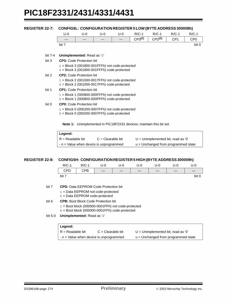
PIC18F2331/2431/4331/4431
REGISTER 22-7: CONFIG5L: CONFIGURATION REGISTER 5 LOW (BYTE ADDRESS 300008h)
REGISTER 22-8: CONFIG5H: CONFIGURATION REGISTER 5 HIGH (BYTE ADDRESS 300009h)
U-0 U-0 U-0 U-0 R/C-1 R/C-1 R/C-1 R/C-1
— — — — CP3(1) CP2(1) CP1 CP0
bit 7 bit 0
bit 7-4 Unimplemented: Read as ‘0’
bit 3 CP3: Code Protection bit
1 = Block 3 (001800-001FFFh) not code-protected 0 = Block 3 (001800-001FFFh) code-protected
bit 2 CP2: Code Protection bit1 = Block 2 (001000-0017FFh) not code-protected 0 = Block 2 (001000-0017FFh) code-protected
bit 1 CP1: Code Protection bit1 = Block 1 (000800-000FFFh) not code-protected 0 = Block 1 (000800-000FFFh) code-protected
bit 0 CP0: Code Protection bit
1 = Block 0 (000200-0007FFh) not code-protected 0 = Block 0 (000200-0007FFh) code-protected
Note 1: Unimplemented in PIC18F2X31 devices; maintain this bit set.
Legend:
R = Readable bit C = Clearable bit U = Unimplemented bit, read as ‘0’
- n = Value when device is unprogrammed u = Unchanged from programmed state
R/C-1 R/C-1 U-0 U-0 U-0 U-0 U-0 U-0
CPD CPB — — — — — —
bit 7 bit 0
bit 7 CPD: Data EEPROM Code Protection bit
1 = Data EEPROM not code-protected0 = Data EEPROM code-protected
bit 6 CPB: Boot Block Code Protection bit1 = Boot block (000000-0001FFh) not code-protected0 = Boot block (000000-0001FFh) code-protected
bit 5-0 Unimplemented: Read as ‘0’
Legend:
R = Readable bit C = Clearable bit U = Unimplemented bit, read as ‘0’
- n = Value when device is unprogrammed u = Unchanged from programmed state
DS39616B-page 274 Preliminary 2003 Microchip Technology Inc.

PIC18F2331/2431/4331/4431
REGISTER 22-9: CONFIG6L: CONFIGURATION REGISTER 6 LOW (BYTE ADDRESS 30000Ah)
REGISTER 22-10: CONFIG6H: CONFIGURATION REGISTER 6 HIGH (BYTE ADDRESS 30000Bh)
U-0 U-0 U-0 U-0 R/P-1 R/P-1 R/P-1 R/P-1
— — — — WRT3(1) WRT2(1) WRT1 WRT0
bit 7 bit 0
bit 7-4 Unimplemented: Read as ‘0’
bit 3 WRT3: Write Protection bit(1)
1 = Block 3 (001800-001FFFh) not write-protected 0 = Block 3 (001800-001FFFh) write-protected
bit 2 WRT2: Write Protection bit(1)
1 = Block 2 (001000-0017FFh) not write-protected 0 = Block 2 (001000-0017FFh) write-protected
bit 1 WRT1: Write Protection bit1 = Block 1 (000800-000FFFh) not write-protected 0 = Block 1 (000800-000FFFh) write-protected
bit 0 WRT0: Write Protection bit
1 = Block 0 (000200-0007FFh) not write-protected 0 = Block 0 (000200-0007FFh) write-protected
Note 1: Unimplemented in PIC18F2X31 devices; maintain this bit set.
Legend:
R = Readable bit P = Programmable bit U = Unimplemented bit, read as ‘0’
- n = Value when device is unprogrammed u = Unchanged from programmed state
R/P-1 R/P-1 R-1 U-0 U-0 U-0 U-0 U-0
WRTD WRTB WRTC — — — — —
bit 7 bit 0
bit 7 WRTD: Data EEPROM Write Protection bit
1 = Data EEPROM not write-protected0 = Data EEPROM write-protected
bit 6 WRTB: Boot Block Write Protection bit1 = Boot block (000000-0001FFh) not write-protected0 = Boot block (000000-0001FFh) write-protected
bit 5 WRTC: Configuration Register Write Protection bit1 = Configuration registers (300000-3000FFh) not write-protected0 = Configuration registers (300000-3000FFh) write-protected
Note: This bit is read-only in normal Execution mode; it can be written only in Program mode.
bit 4-0 Unimplemented: Read as ‘0’
Legend:
R = Readable bit P = Programmable bit U = Unimplemented bit, read as ‘0’
- n = Value when device is unprogrammed u = Unchanged from programmed state
2003 Microchip Technology Inc. Preliminary DS39616B-page 275

PIC18F2331/2431/4331/4431
REGISTER 22-11: CONFIG7L: CONFIGURATION REGISTER 7 LOW (BYTE ADDRESS 30000Ch)
REGISTER 22-12: CONFIG7H: CONFIGURATION REGISTER 7 HIGH (BYTE ADDRESS 30000Dh)
U-0 U-0 U-0 U-0 R/P-1 R/P-1 R/P-1 R/P-1
— — — — EBTR3(1) EBTR2(1) EBTR1 EBTR0
bit 7 bit 0
bit 7-4 Unimplemented: Read as ‘0’
bit 3 EBTR3: Table Read Protection bit(1)
1 = Block 3 (001800-001FFFh) not protected from table reads executed in other blocks0 = Block 3 (001800-001FFFh) protected from table reads executed in other blocks
bit 2 EBTR2: Table Read Protection bit(1)
1 = Block 2 (001000-0017FFh) not protected from table reads executed in other blocks 0 = Block 2 (001000-0017FFh) protected from table reads executed in other blocks
bit 1 EBTR1: Table Read Protection bit1 = Block 1 (000800-000FFFh) not protected from table reads executed in other blocks 0 = Block 1 (000800-000FFFh) protected from table reads executed in other blocks
bit 0 EBTR0: Table Read Protection bit
1 = Block 0 (000200-0007FFh) not protected from table reads executed in other blocks 0 = Block 0 (000200-0007FFh) protected from table reads executed in other blocks
Note 1: Unimplemented in PIC18F2X31 devices; maintain this bit set.
Legend:
R = Readable bit P = Programmable bit U = Unimplemented bit, read as ‘0’
- n = Value when device is unprogrammed u = Unchanged from programmed state
U-0 R/P-1 U-0 U-0 U-0 U-0 U-0 U-0
— EBTRB — — — — — —
bit 7 bit 0
bit 7 Unimplemented: Read as ‘0’
bit 6 EBTRB: Boot Block Table Read Protection bit1 = Boot block (000000-0001FFh) not protected from table reads executed in other blocks0 = Boot block (000000-0001FFh) protected from table reads executed in other blocks
bit 5-0 Unimplemented: Read as ‘0’
Legend:
R = Readable bit P = Programmable bit U = Unimplemented bit, read as ‘0’
- n = Value when device is unprogrammed u = Unchanged from programmed state
DS39616B-page 276 Preliminary 2003 Microchip Technology Inc.

PIC18F2331/2431/4331/4431
REGISTER 22-13: DEVICE ID REGISTER 1 FOR PIC18F2331/2431/4331/4431 DEVICES
REGISTER 22-14: DEVICE ID REGISTER 2 FOR PIC18F2331/2431/4331/4431 DEVICES
R R R R R R R R
DEV2 DEV1 DEV0 REV4 REV3 REV2 REV1 REV0
bit 7 bit 0
bit 7-5 DEV<2:0>: Device ID bitsThese bits are used with the DEV<10:3> bits in the Device ID register 2 to identify the part number.000 = PIC18F4331001 = PIC18F4431
100 = PIC18F2331101 = PIC18F2431
bit 4-0 REV<4:0>: Revision ID bitsThese bits are used to indicate the device revision.
Legend:
R = Read-only bit P = Programmable bit U = Unimplemented bit, read as ‘0’
- n = Value when device is unprogrammed u = Unchanged from programmed state
R R R R R R R R
DEV10 DEV9 DEV8 DEV7 DEV6 DEV5 DEV4 DEV3
bit 7 bit 0
bit 7-0 DEV10:DEV3: Device ID bits
These bits are used with the DEV2:DEV0 bits in the Device ID Register 1 to identify the part number
0000 0101 = PIC18F2331/2431/4331/4431 devices
Note 1: These values for DEV10:DEV3 may be shared with other devices. The specificdevice is always identified by using the entire DEV10:DEV0 bit sequence.
Legend:
R = Read-only bit P = Programmable bit U = Unimplemented bit, read as ‘0’
- n = Value when device is unprogrammed u = Unchanged from programmed state
2003 Microchip Technology Inc. Preliminary DS39616B-page 277

PIC18F2331/2431/4331/4431
22.2 Watchdog Timer (WDT)
For PIC18F2331/2431/4331/4431 devices, the WDT isdriven by the INTRC source. When the WDT isenabled, the clock source is also enabled. The nominalWDT period is 4 ms and has the same stability as theINTRC oscillator.
The 4 ms period of the WDT is multiplied by a 16-bitpostscaler. Any output of the WDT postscaler isselected by a multiplexer, controlled by bits inConfiguration Register 2H (see Register 22-3).Available periods range from 4 ms to 131.072 seconds(2.18 minutes). The WDT and postscaler are clearedwhen any of the following events occur: execute aSLEEP or CLRWDT instruction, the IRCF bits(OSCCON<6:4>) are changed, or a clock failure hasoccurred (see Section 22.4.1 “FSCM and theWatchdog Timer”).
Adjustments to the internal oscillator clock period usingthe OSCTUNE register also affect the period of theWDT by the same factor. For example, if the INTRCperiod is increased by 3%, then the WDT period isincreased by 3%.
22.2.1 CONTROL REGISTER
Register 22-15 shows the WDTCON register. This is areadable and writable register. The SWDTEN bit allowssoftware to enable or disable the WDT, but only if theconfiguration bit has disabled the WDT. The WDTW bitis a read-only bit that indicates when the WDT count isin the fourth quadrant (i.e., when the 8-bit WDT value isb’11000000’ or greater).
FIGURE 22-1: WDT BLOCK DIAGRAM
REGISTER 22-15: WDTCON REGISTER
Note 1: The CLRWDT and SLEEP instructionsclear the WDT and postscaler countswhen executed.
2: Changing the setting of the IRCF bits(OSCCON<6:4> clears the WDT andpostscaler counts.
3: When a CLRWDT instruction is executedthe postscaler count will be cleared.
4: If WINEN = 0, then CLRWDT must beexecuted only when WDTW = 1; other-wise, a device reset will result.
R-0 U-0 U-0 U-0 U-0 U-0 U-0 R/W-0
WDTW — — — — — — SWDTEN
bit 7 bit 0
bit 7 WDTW: Watchdog Timer Window bit1 = WDT count is in fourth quadrant0 = WDT count is not in fourth quadrant
bit 6 Unimplemented
bit 0 SWDTEN: Software Enable / Disable for Watch Dog Timer bit (1) 1 = WDT is turned on0 = WDT is turned off
Note 1: If WDTEN configuration bit = 1, then WDT is always enabled, irrespective of this controlbit. If WDTEN configuration bit = 0, then it is possible to turn WDT on/off with this con-trol bit.
Legend:
R = Readable bit W = Writable bit
U = Unimplemented bit, read as ‘0’ - n = Value at POR
INTRC Source
WDT
Wake-up
Reset
WDT
WDT Counter
Programmable Postscaler1:1 to 1:32,768
Enable WDT
WDTPS<3:0>
SWDTENWDTEN
CLRWDT
4
from Sleep
Reset
All Device Resets
Sleep
INTRC Control
÷125
Change on IRCF Bits
DS39616B-page 278 Preliminary 2003 Microchip Technology Inc.

PIC18F2331/2431/4331/4431
TABLE 22-2: SUMMARY OF WATCHDOG TIMER REGISTERS
22.3 Two-Speed Start-up
The Two-Speed Start-up feature helps to minimize thelatency period from oscillator start-up to code executionby allowing the microcontroller to use the INTRC oscil-lator as a clock source until the primary clock source isavailable. It is enabled by setting the IESO bit inConfiguration Register 1H (CONFIG1H<7>).
Two-Speed Start-up is available only if the primaryOscillator mode is LP, XT, HS or HSPLL (crystal-basedmodes). Other sources do not require a OST start-updelay; for these, Two-Speed Start-up is disabled.
When enabled, Resets and wake-ups from Sleep modecause the device to configure itself to run from the inter-nal oscillator block as the clock source, following thetime-out of the Power-up Timer after a POR Reset isenabled. This allows almost immediate code execu-tion, while the primary oscillator starts and the OST isrunning. Once the OST times out, the device automat-ically switches to PRI_RUN mode.
Because the OSCCON register is cleared on Resetevents, the INTOSC (or postscaler) clock source is notinitially available after a Reset event; the INTRC clockis used directly at its base frequency. To use a higherclock speed on wake-up, the INTOSC or postscalerclock sources can be selected to provide a higher clockspeed by setting bits IFRC2:IFRC0 immediately afterReset. For wake-ups from Sleep, the INTOSC orpostscaler clock sources can be selected by settingIFRC2:IFRC0 prior to entering Sleep mode.
In all other power-managed modes, Two-Speed Start-up is not used. The device will be clocked by the cur-rently selected clock source until the primary clocksource becomes available. The setting of the IESO bitis ignored.
22.3.1 SPECIAL CONSIDERATIONS FOR USING TWO-SPEED START-UP
While using the INTRC oscillator in Two-Speed Start-up, the device still obeys the normal commandsequences for entering power-managed modes,including serial SLEEP instructions (refer toSection 3.1.3 “Multiple Sleep Commands”). In prac-tice, this means that user code can change theSCS1:SCS0 bit settings and issue SLEEP commandsbefore the OST times out. This would allow an applica-tion to briefly wake-up, perform routine “housekeeping”tasks and return to Sleep before the device starts tooperate from the primary oscillator.
User code can also check if the primary clock source iscurrently providing the system clocking by checking thestatus of the OSTS bit (OSCCON<3>). If the bit is set,the primary oscillator is providing the system clock.Otherwise, the internal oscillator block is providing theclock during wake-up from Reset or Sleep mode.
Name Bit 7 Bit 6 Bit 5 Bit 4 Bit 3 Bit 2 Bit 1 Bit 0
CONFIG2H — — WINEN WDTPS3 WDTPS2 WDTPS2 WDTPS0 WDTEN
RCON IPEN — — RI TO PD POR BOR
WDTCON WDTW — — — — — — SWDTEN
Legend: Shaded cells are not used by the Watchdog Timer.
2003 Microchip Technology Inc. Preliminary DS39616B-page 279

PIC18F2331/2431/4331/4431
FIGURE 22-2: TIMING TRANSITION FOR TWO-SPEED START-UP (INTOSC TO HSPLL) Q1 Q3 Q4
OSC1
Peripheral
Program PC PC + 2
INTOSC
PLL Clock
Q1
PC + 6
Q2
Output
Q3 Q4 Q1
CPU Clock
PC + 4
Clock
Counter
Q2 Q2 Q3 Q4
Note 1: TOST = 1024 TOSC; TPLL = 2 ms (approx). These intervals are not shown to scale.
Wake from Interrupt Event
TOST(1)TPLL(1)
1 2 3 4 5 6 7 8Clock Transition
OSTS bit Set
Multiplexer
DS39616B-page 280 Preliminary 2003 Microchip Technology Inc.

PIC18F2331/2431/4331/4431
22.4 Fail-Safe Clock Monitor
The Fail-Safe Clock Monitor (FSCM) allows themicrocontroller to continue operation in the event of anexternal oscillator failure, by automatically switchingthe system clock to the internal oscillator block. TheFSCM function is enabled by setting the Fail-SafeClock Monitor Enable bit, FCMEN (CONFIG1H<6>).
When FSCM is enabled, the INTRC oscillator runs atall times to monitor clocks to peripherals and providean instant backup clock in the event of a clock failure.Clock monitoring (shown in Figure 22-3) isaccomplished by creating a sample clock signal, whichis the INTRC output divided by 64. This allows ampletime between FSCM sample clocks for a peripheralclock edge to occur. The peripheral system clock andthe sample clock are presented as inputs to the ClockMonitor latch (CM). The CM is set on the falling edge ofthe system clock source, but cleared on the rising edgeof the sample clock.
FIGURE 22-3: FSCM BLOCK DIAGRAM
Clock failure is tested for on the falling edge of thesample clock. If a sample clock falling edge occurswhile CM is still set, a clock failure has been detected(Figure 22-4). This causes the following:
• the FSCM generates an oscillator fail interrupt by setting bit OSCFIF (PIR2<7>);
• the system clock source is switched to the internal oscillator block (OSCCON is not updated to show the current clock source – this is the fail-safe condition); and
• the WDT is reset.
Since the postscaler frequency from the internaloscillator block may not be sufficiently stable, it may bedesirable to select another clock configuration andenter an alternate power-managed mode (seeSection 22.3.1 “Special Considerations for UsingTwo-Speed Start-up” and Section 3.1.3 “MultipleSleep Commands” for more details). This can bedone to attempt a partial recovery or execute acontrolled shutdown.
To use a higher clock speed on wake-up, the INTOSCor postscaler clock sources can be selected to providea higher clock speed by setting bits IFRC2:IFRC0immediately after Reset. For wake-ups from Sleep, theINTOSC or postscaler clock sources can be selectedby setting IFRC2:IFRC0 prior to entering Sleep mode.
Adjustments to the internal oscillator block using theOSCTUNE register also affect the period of the FSCMby the same factor. This can usually be neglected, asthe clock frequency being monitored is generally muchhigher than the sample clock frequency.
The FSCM will detect failures of the primary or second-ary clock sources only. If the internal oscillator blockfails, no failure would be detected, nor would any actionbe possible.
22.4.1 FSCM AND THE WATCHDOG TIMER
Both the FSCM and the WDT are clocked by theINTRC oscillator. Since the WDT operates with aseparate divider and counter, disabling the WDT hasno effect on the operation of the INTRC oscillator whenthe FSCM is enabled.
As already noted, the clock source is switched to theINTOSC clock when a clock failure is detected.Depending on the frequency selected by theIRCF2:IRCF0 bits, this may mean a substantial changein the speed of code execution. If the WDT is enabledwith a small prescale value, a decrease in clock speedallows a WDT time-out to occur, and a subsequentdevice Reset. For this reason, fail-safe clock eventsalso reset the WDT and postscaler, allowing it to starttiming from when execution speed was changed anddecreasing the likelihood of an erroneous time-out.
22.4.2 EXITING FAIL-SAFE OPERATION
The fail-safe condition is terminated by either a deviceReset, or by entering a power-managed mode. On Reset,the controller starts the primary clock source specified inConfiguration Register 1H (with any required start-updelays that are required for the Oscillator mode, such asOST or PLL timer). The INTOSC multiplexer provides thesystem clock until the primary clock source becomesready (similar to a Two-Speed Start-up). The clock systemsource is then switched to the primary clock (indicated bythe OSTS bit in the OSCCON register becoming set). TheFail-Safe Clock Monitor then resumes monitoring theperipheral clock.
The primary clock source may never become readyduring start-up. In this case, operation is clocked by theINTOSC multiplexer. The OSCCON register will remain inits Reset state until a power-managed mode is entered.
Entering a power-managed mode by loading theOSCCON register and executing a SLEEP instructionwill clear the fail-safe condition. When the fail-safecondition is cleared, the clock monitor will resumemonitoring the peripheral clock.
Peripheral
INTRC÷ 64
S
C
Q
(32 µs) 488 Hz(2.048 ms)
Clock MonitorLatch (CM)
(edge-triggered)
ClockFailure
Detected
Source
Clock
Q
2003 Microchip Technology Inc. Preliminary DS39616B-page 281

PIC18F2331/2431/4331/4431
FIGURE 22-4: FSCM TIMING DIAGRAM
22.4.3 FSCM INTERRUPTS IN POWER-MANAGED MODES
As previously mentioned, entering a power-managedmode clears the fail-safe condition. By entering apower-managed mode, the clock multiplexer selectsthe clock source selected by the OSCCON register.Fail-safe monitoring of the power-managed clocksource resumes in the power-managed mode.
If an oscillator failure occurs during power-managedoperation, the subsequent events depend on whetheror not the oscillator failure interrupt is enabled. Ifenabled (OSCFIF = 1), code execution will be clockedby the INTOSC multiplexer. An automatic transitionback to the failed clock source will not occur.
If the interrupt is disabled, the device will not exit thepower-managed mode on oscillator failure. Instead, thedevice will continue to operate as before, but clockedby the INTOSC multiplexer. While in Idle mode, subse-quent interrupts will cause the CPU to begin executinginstructions while being clocked by the INTOSC multi-plexer. The device will not transition to a different clocksource until the fail-safe condition is cleared.
22.4.4 POR OR WAKE FROM SLEEP
The FSCM is designed to detect oscillator failure at anypoint after the device has exited Power-on Reset(POR) or Low-Power Sleep mode. When the primarysystem clock is EC, RC or INTRC modes, monitoringcan begin immediately following these events.
For oscillator modes involving a crystal or resonator(HS, HSPLL, LP or XT), the situation is somewhatdifferent. Since the oscillator may require a start-uptime considerably longer than the FCSM sample clocktime, a false clock failure may be detected. To preventthis, the internal oscillator block is automaticallyconfigured as the system clock and functions until theprimary clock is stable (the OST and PLL timers havetimed out). This is identical to Two-Speed Start-upmode. Once the primary clock is stable, the INTRCreturns to its role as the FSCM source.
As noted in Section 22.3.1 “Special Considerationsfor Using Two-Speed Start-up”, it is also possible toselect another clock configuration and enter analternate power-managed mode, while waiting for theprimary system clock to become stable. When the newPowered Managed mode is selected, the primary clockis disabled.
OSCFIF
CM Output
SystemClock
Output
Sample Clock
FailureDetected
OscillatorFailure
Note: The system clock is normally at a much higher frequency than the sample clock. The relative frequencies inthis example have been chosen for clarity.
(Q)
CM Test CM Test CM Test
Note: The same logic that prevents falseoscillator failure interrupts on POR orwake from Sleep will also prevent thedetection of the oscillator’s failure to startat all following these events. This can beavoided by monitoring the OSTS bit andusing a timing routine to determine if theoscillator is taking too long to start. Evenso, no oscillator failure interrupt will beflagged.
DS39616B-page 282 Preliminary 2003 Microchip Technology Inc.

PIC18F2331/2431/4331/4431
22.5 Program Verification and Code Protection
The overall structure of the code protection on thePIC18 Flash devices differs significantly from otherPICmicro® devices.
The user program memory is divided into five blocks.One of these is a boot block of 512 bytes. Theremainder of the memory is divided into four blocks onbinary boundaries.
Each of the five blocks has three code protection bitsassociated with them. They are:
• Code-Protect bit (CPn)• Write-Protect bit (WRTn)• External Block Table Read bit (EBTRn)
Figure 22-5 shows the program memory organizationfor 8- and 16-Kbyte devices, and the specific codeprotection bit associated with each block. The actuallocations of the bits are summarized in Table 22-3.
FIGURE 22-5: CODE-PROTECTED PROGRAM MEMORY FOR PIC18F2331/2431/4331/4431
TABLE 22-3: SUMMARY OF CODE PROTECTION REGISTERS
MEMORY SIZE/DEVICE
Block Code Protection Controlled By:
8 Kbytes(PIC18FX331)
Address Range
16 Kbytes(PIC18FX431)
Address Range
Boot Block0000h0FFFh
Boot Block0000h01FFh
CPB, WRTB, EBTRB
Block 00200h
0FFFhBlock 0
0200h
0FFFhCP0, WRT0, EBTR0
Block 11000h
1FFFhBlock 1
1000h
1FFFhCP1, WRT1, EBTR1
UnimplementedRead 0’s
Block 22000h
2FFFhCP2, WRT2, EBTR2
3FFFhBlock 3
3000h
3FFFhCP3, WRT3, EBTR3
File Name Bit 7 Bit 6 Bit 5 Bit 4 Bit 3 Bit 2 Bit 1 Bit 0
300008h CONFIG5L — — — — CP3 CP2 CP1 CP0
300009h CONFIG5H CPD CPB — — — — — —
30000Ah CONFIG6L — — — — WRT3 WRT2 WRT1 WRT0
30000Bh CONFIG6H WRTD WRTB WRTC — — — — —
30000Ch CONFIG7L — — — — EBTR3 EBTR2 EBTR1 EBTR0
30000Dh CONFIG7H — EBTRB — — — — — —
Legend: Shaded cells are unimplemented.
2003 Microchip Technology Inc. Preliminary DS39616B-page 283

PIC18F2331/2431/4331/4431
22.5.1 PROGRAM MEMORYCODE PROTECTION
The program memory may be read to or written fromany location using the table read and table writeinstructions. The device ID may be read with tablereads. The configuration registers may be read andwritten with the table read and table write instructions.
In normal Execution mode, the CPn bits have no directeffect. CPn bits inhibit external reads and writes. A blockof user memory may be protected from table writes if theWRTn configuration bit is ‘0’. The EBTRn bits controltable reads. For a block of user memory with the EBTRnbit set to ‘0’, a table read instruction that executes fromwithin that block is allowed to read. A table read instruc-tion that executes from a location outside of that block isnot allowed to read, and will result in reading ‘0’s.Figures 22-6 through 22-8 illustrate table write and tableread protection.
FIGURE 22-6: TABLE WRITE (WRTn) DISALLOWED
Note: Code protection bits may only be written toa ‘0’ from a ‘1’ state. It is not possible towrite a ‘1’ to a bit in the ‘0’ state. Codeprotection bits are only set to ‘1’ by a fullchip erase or block erase function. The fullchip erase and block erase functions canonly be initiated via ICSP or an externalprogrammer.
000000h
0001FFh000200h
0007FFh000800h
000FFFh001000h
0017FFh001800h
001FFFh
WRTB,EBTRB = 11
WRT0,EBTR0 = 01
WRT1,EBTR1 = 11
WRT2,EBTR2 = 11
WRT3,EBTR3 = 11
TBLWT *
TBLPTR = 0002FFh
PC = 0007FEh
TBLWT *PC = 0017FEh
Register Values Program Memory Configuration Bit Settings
Results: All table writes disabled to Blockn whenever WRTn = ‘0’.
DS39616B-page 284 Preliminary 2003 Microchip Technology Inc.

PIC18F2331/2431/4331/4431
FIGURE 22-7: EXTERNAL BLOCK TABLE READ (EBTRn) DISALLOWED
FIGURE 22-8: EXTERNAL BLOCK TABLE READ (EBTRn) ALLOWED
000000h
0001FFh000200h
0007FFh000800h
000FFFh001000h
0017FFh001800h
001FFFh
WRTB,EBTRB = 11
WRT0,EBTR0 = 10
WRT1,EBTR1 = 11
WRT2,EBTR2 = 11
WRT3,EBTR3 = 11
TBLRD *
TBLPTR = 0002FFh
PC = 000FFEh
Results: All table reads from external blocks to Blockn are disabled whenever EBTRn = ‘0’. TABLAT register returns a value of ‘0’.
Register Values Program Memory Configuration Bit Settings
000000h
0001FFh000200h
0007FFh000800h
000FFFh001000h
0017FFh001800h
001FFFh
WRTB,EBTRB = 11
WRT0,EBTR0 = 10
WRT1,EBTR1 = 11
WRT2,EBTR2 = 11
WRT3,EBTR3 = 11
TBLRD *
TBLPTR = 0002FFh
PC = 0007FEh
Register Values Program Memory Configuration Bit Settings
Results: Table reads permitted within Blockn, even when EBTRBn = ‘0’. TABLAT register returns the value of the data at the location TBLPTR.
2003 Microchip Technology Inc. Preliminary DS39616B-page 285

PIC18F2331/2431/4331/4431
22.5.2 DATA EEPROM CODE PROTECTION
The entire data EEPROM is protected from externalreads and writes by two bits: CPD and WRTD. CPDinhibits external reads and writes of data EEPROM.WRTD inhibits external writes to data EEPROM. TheCPU can continue to read and write data EEPROMregardless of the protection bit settings.
22.5.3 CONFIGURATION REGISTER PROTECTION
The configuration registers can be write-protected. TheWRTC bit controls protection of the configurationregisters. In normal Execution mode, the WRTC bit isreadable only. WRTC can only be written via ICSP oran external programmer.
22.6 ID Locations
Eight memory locations (200000h-200007h) aredesignated as ID locations, where the user can storechecksum or other code identification numbers. Theselocations are both readable and writable during normalexecution through the TBLRD and TBLWT instructions,or during program/verify. The ID locations can be readwhen the device is code-protected.
22.7 In-Circuit Serial Programming
PIC18F2331/2431/4331/4431 microcontrollers can beserially programmed while in the end application circuit.This is simply done with two lines for clock and data,and three other lines for power, ground and the pro-gramming voltage. This allows customers to manufac-ture boards with unprogrammed devices, and thenprogram the microcontroller just before shipping theproduct. This also allows the most recent firmware or acustom firmware to be programmed.
22.8 In-Circuit Debugger
When the DEBUG bit in configuration registerCONFIG4L is programmed to a ‘0’, the In-CircuitDebugger functionality is enabled. This function allowssimple debugging functions when used with MPLAB®
IDE. When the microcontroller has this featureenabled, some resources are not available for generaluse. Table 22-4 shows which resources are required bythe background debugger.
TABLE 22-4: DEBUGGER RESOURCES
To use the In-Circuit Debugger function of the micro-controller, the design must implement In-Circuit SerialProgramming connections to MCLR/VPP, VDD, VSS,RB7 and RB6. This will interface to the In-CircuitDebugger module available from Microchip or one ofthe third party development tool companies.
22.9 Low-Voltage ICSP Programming
The LVP bit in Configuration Register 4L(CONFIG4L<2>) enables Low-Voltage ICSP Program-ming (LVP). When LVP is enabled, the microcontrollercan be programmed without requiring high voltagebeing applied to the MCLR/VPP pin, but the RB5/PGMpin is then dedicated to controlling Program mode entryand is not available as a general purpose I/O pin.
LVP is enabled in erased devices.
While programming using LVP, VDD is applied to theMCLR/VPP pin as in normal Execution mode. To enterProgramming mode, VDD is applied to the PGM pin.
If Low-Voltage ICSP Programming mode will not beused, the LVP bit can be cleared and RB5/PGMbecomes available as the digital I/O pin RB5. The LVPbit may be set or cleared only when using standard highvoltage programming (VIHH applied to the MCLR/VPP
pin). Once LVP has been disabled, only the standardhigh voltage programming is available and must beused to program the device.
Memory that is not code-protected can be erased usingeither a block erase, or erased row by row, then writtenat any specified VDD. If code-protected memory is to beerased, a block erase is required. If a block erase is tobe performed when using low-voltage programming,the device must be supplied with VDD of 4.5V to 5.5V.
I/O pins: RB6, RB7
Stack: 2 levels
Program Memory: 512 bytes
Data Memory: 10 bytes
Note 1: High voltage programming is alwaysavailable, regardless of the state of theLVP bit or the PGM pin, by applying VIHH
to the MCLR pin.
2: When Low-Voltage Programming isenabled, the RB5 pin can no longer beused as a general purpose I/O pin.
3: When LVP is enabled, externally pull thePGM pin to VSS to allow normal programexecution.
DS39616B-page 286 Preliminary 2003 Microchip Technology Inc.

PIC18F2331/2431/4331/4431
23.0 INSTRUCTION SET SUMMARY
The PIC18 instruction set adds many enhancements tothe previous PICmicro instruction sets, while maintain-ing an easy migration from these PICmicro instructionsets.
Most instructions are a single program memory word(16-bits), but there are three instructions that requiretwo program memory locations.
Each single-word instruction is a 16-bit word dividedinto an OPCODE, which specifies the instruction typeand one or more operands, which further specify theoperation of the instruction.
The instruction set is highly orthogonal and is groupedinto four basic categories:
• Byte-oriented operations• Bit-oriented operations• Literal operations
• Control operations
The PIC18 instruction set summary in Table 23-2 listsbyte-oriented, bit-oriented, literal and control opera-tions. Table 23-1 shows the OPCODE field descriptions.
Most byte-oriented instructions have three operands:
1. The file register (specified by ‘f’) 2. The destination of the result
(specified by ‘d’) 3. The accessed memory
(specified by ‘a’)
The file register designator 'f' specifies which fileregister is to be used by the instruction.
The destination designator ‘d’ specifies where theresult of the operation is to be placed. If 'd' is zero, theresult is placed in the WREG register. If 'd' is one, theresult is placed in the file register specified in theinstruction.
All bit-oriented instructions have three operands:
1. The file register (specified by ‘f’)
2. The bit in the file register (specified by ‘b’)
3. The accessed memory (specified by ‘a’)
The bit field designator 'b' selects the number of the bitaffected by the operation, while the file register desig-nator 'f' represents the number of the file in which thebit is located.
The literal instructions may use some of the followingoperands:
• A literal value to be loaded into a file register (specified by ‘k’)
• The desired FSR register to load the literal value into (specified by ‘f’)
• No operand required (specified by ‘—’)
The control instructions may use some of the followingoperands:
• A program memory address (specified by ‘n’)• The mode of the Call or Return instructions
(specified by ‘s’)• The mode of the table read and table write
instructions (specified by ‘m’)• No operand required
(specified by ‘—’)
All instructions are a single word, except for three dou-ble word instructions. These three instructions weremade double word instructions so that all the requiredinformation is available in these 32 bits. In the secondword, the 4 MSbs are 1’s. If this second word isexecuted as an instruction (by itself), it will execute asa NOP.
All single-word instructions are executed in a singleinstruction cycle, unless a conditional test is true or theprogram counter is changed as a result of the instruc-tion. In these cases, the execution takes two instructioncycles with the additional instruction cycle(s) executedas a NOP.
The double word instructions execute in two instructioncycles.
One instruction cycle consists of four oscillator periods.Thus, for an oscillator frequency of 4 MHz, the normalinstruction execution time is 1 µs. If a conditional test istrue or the program counter is changed as a result of aninstruction, the instruction execution time is 2 µs. Two-word branch instructions (if true) would take 3 µs.
Figure 23-1 shows the general formats that the instruc-tions can have.
All examples use the format ‘nnh’ to represent a hexa-decimal number, where ‘h’ signifies a hexadecimaldigit.
The Instruction Set Summary, shown in Table 23-2,lists the instructions recognized by the MicrochipAssembler (MPASMTM assembler). Section 23.2“Instruction Set” provides a description of eachinstruction.
23.1 READ-MODIFY-WRITE OPERATIONS
Any instruction that specifies a file register as part ofthe instruction performs a Read-Modify-Write (R-M-W)operation. The register is read, the data is modified,and the result is stored according to either the instruc-tion or the destination designator ‘d’. A read operationis performed on a register even if the instruction writesto that register.
For example, a "BCF PORTB,1" instruction will readPORTB, clear bit 1 of the data, then write the resultback to PORTB. The read operation would have theunintended result that any condition that sets the RBIFflag would be cleared. The R-M-W operation may alsocopy the level of an input pin to its corresponding outputlatch.
2003 Microchip Technology Inc. Preliminary DS39616B-page 287

PIC18F2331/2431/4331/4431
TABLE 23-1: OPCODE FIELD DESCRIPTIONS
Field Description
a RAM access bit:a = 0: RAM location in Access RAM (BSR register is ignored)a = 1: RAM bank is specified by BSR register
bbb Bit address within an 8-bit file register (0 to 7).
BSR Bank Select Register. Used to select the current RAM bank.
d Destination select bit:d = 0: store result in WREGd = 1: store result in file register f
dest Destination either the WREG register or the specified register file location.
f 8-bit register file address (0x00 to 0xFF).
fs 12-bit register file address (0x000 to 0xFFF). This is the source address.
fd 12-bit register file address (0x000 to 0xFFF). This is the destination address.
k Literal field, constant data or label (may be either an 8-bit, 12-bit or a 20-bit value).
label Label name.
mm The mode of the TBLPTR register for the table read and table write instructions.Only used with table read and table write instructions:
* No Change to register (such as TBLPTR with table reads and writes).
*+ Post-Increment register (such as TBLPTR with table reads and writes).
*- Post-Decrement register (such as TBLPTR with table reads and writes).
+* Pre-Increment register (such as TBLPTR with table reads and writes).
n The relative address (2’s complement number) for relative branch instructions, or the direct address for Call/Branch and Return instructions.
PRODH Product of Multiply high byte.
PRODL Product of Multiply low byte.
s Fast Call/Return Mode Select bit:s = 0: do not update into/from shadow registerss = 1: certain registers loaded into/from shadow registers (Fast mode)
u Unused or Unchanged.
WREG Working register (accumulator).
x Don't care (0 or 1) .The assembler will generate code with x = 0. It is the recommended form of use for compatibility with all Microchip software tools.
TBLPTR 21-bit Table Pointer (points to a Program Memory location).
TABLAT 8-bit Table Latch.
TOS Top-of-Stack.
PC Program Counter.
PCL Program Counter Low Byte.
PCH Program Counter High Byte.
PCLATH Program Counter High Byte Latch.
PCLATU Program Counter Upper Byte Latch.
GIE Global Interrupt Enable bit.
WDT Watchdog Timer.
TO Time-out bit.
PD Power-down bit.
C, DC, Z, OV, N ALU status bits Carry, Digit Carry, Zero, Overflow, Negative.
[ ] Optional.
( ) Contents.
→ Assigned to.
< > Register bit field.
∈ In the set of.
italics User defined term (font is courier).
DS39616B-page 288 Preliminary 2003 Microchip Technology Inc.

PIC18F2331/2431/4331/4431
FIGURE 23-1: GENERAL FORMAT FOR INSTRUCTIONS
Byte-oriented file register operations
15 10 9 8 7 0
d = 0 for result destination to be WREG register
OPCODE d a f (FILE #)
d = 1 for result destination to be file register (f)a = 0 to force Access Bank
Bit-oriented file register operations
15 12 11 9 8 7 0
OPCODE b (BIT #) a f (FILE #)
b = 3-bit position of bit in file register (f)
Literal operations
15 8 7 0
OPCODE k (literal)
k = 8-bit immediate value
Byte to Byte move operations (2-word)
15 12 11 0
OPCODE f (Source FILE #)
CALL, GOTO and Branch operations
15 8 7 0
OPCODE n<7:0> (literal)
n = 20-bit immediate value
a = 1 for BSR to select bankf = 8-bit file register address
a = 0 to force Access Banka = 1 for BSR to select bankf = 8-bit file register address
15 12 11 0
1111 n<19:8> (literal)
15 12 11 0
1111 f (Destination FILE #)
f = 12-bit file register address
Control operations
Example Instruction
ADDWF MYREG, W, B
MOVFF MYREG1, MYREG2
BSF MYREG, bit, B
MOVLW 0x7F
GOTO Label
15 8 7 0
OPCODE n<7:0> (literal)
15 12 11 0
n<19:8> (literal)
CALL MYFUNC
15 11 10 0
OPCODE n<10:0> (literal)
S = Fast bit
BRA MYFUNC
15 8 7 0
OPCODE n<7:0> (literal) BC MYFUNC
S
2003 Microchip Technology Inc. Preliminary DS39616B-page 289

PIC18F2331/2431/4331/4431
TABLE 23-2: PIC18FXXX INSTRUCTION SET
Mnemonic,Operands
Description Cycles16-Bit Instruction Word Status
AffectedNotes
MSb LSb
BYTE-ORIENTED FILE REGISTER OPERATIONS
ADDWFADDWFCANDWFCLRFCOMFCPFSEQCPFSGTCPFSLTDECFDECFSZDCFSNZINCFINCFSZINFSNZIORWFMOVFMOVFF
MOVWFMULWFNEGFRLCFRLNCFRRCFRRNCFSETFSUBFWB
SUBWFSUBWFB
SWAPFTSTFSZXORWF
f, d, af, d, af, d, af, af, d, af, af, af, af, d, af, d, af, d, af, d, af, d, af, d, af, d, af, d, afs, fd
f, af, af, af, d, af, d, af, d, af, d, af, af, d, a
f, d, af, d, a
f, d, af, af, d, a
Add WREG and fAdd WREG and Carry bit to fAND WREG with fClear fComplement fCompare f with WREG, skip =Compare f with WREG, skip >Compare f with WREG, skip <Decrement fDecrement f, Skip if 0Decrement f, Skip if Not 0Increment fIncrement f, Skip if 0Increment f, Skip if Not 0Inclusive OR WREG with fMove fMove fs (source) to 1st word
fd (destination) 2nd wordMove WREG to fMultiply WREG with fNegate fRotate Left f through CarryRotate Left f (No Carry)Rotate Right f through CarryRotate Right f (No Carry)Set fSubtract f from WREG with borrow Subtract WREG from fSubtract WREG from f with borrowSwap nibbles in fTest f, skip if 0Exclusive OR WREG with f
111111 (2 or 3)1 (2 or 3)1 (2 or 3)11 (2 or 3)1 (2 or 3)11 (2 or 3)1 (2 or 3)112
111111111
11
11 (2 or 3)1
001000100001011000010110011001100000001001000010001101000001010111001111011000000110001101000011010001100101
01010101
001101100001
01da00da01da101a11da001a010a000a01da11da11da10da11da10da00da00daffffffff111a001a110a01da01da00da00da100a01da
11da10da
10da011a10da
ffffffffffffffffffffffffffffffffffffffffffffffffffffffffffffffffffffffffffffffffffffffffffffffffffffffffffff
ffffffff
ffffffffffff
ffffffffffffffffffffffffffffffffffffffffffffffffffffffffffffffffffffffffffffffffffffffffffffffffffffffffffff
ffffffff
ffffffffffff
C, DC, Z, OV, NC, DC, Z, OV, NZ, NZZ, NNoneNoneNoneC, DC, Z, OV, NNoneNoneC, DC, Z, OV, NNoneNoneZ, NZ, NNone
NoneNoneC, DC, Z, OV, NC, Z, NZ, NC, Z, NZ, NNoneC, DC, Z, OV, N
C, DC, Z, OV, NC, DC, Z, OV, N
NoneNoneZ, N
1, 21, 21,221, 2441, 21, 2, 3, 41, 2, 3, 41, 21, 2, 3, 441, 21, 21
1, 2
1, 2
1, 2
1, 2
41, 2
BIT-ORIENTED FILE REGISTER OPERATIONS
BCFBSFBTFSCBTFSSBTG
f, b, af, b, af, b, af, b, af, d, a
Bit Clear fBit Set fBit Test f, Skip if ClearBit Test f, Skip if SetBit Toggle f
111 (2 or 3)1 (2 or 3)1
10011000101110100111
bbbabbbabbbabbbabbba
ffffffffffffffffffff
ffffffffffffffffffff
NoneNoneNoneNoneNone
1, 21, 23, 43, 41, 2
Note 1: When a PORT register is modified as a function of itself (e.g., MOVF PORTB, 1, 0), the value used will be that value present on the pins themselves. For example, if the data latch is ‘1’ for a pin configured as input and is driven low by an external device, the data will be written back with a ‘0’.
2: If this instruction is executed on the TMR0 register (and, where applicable, d = 1), the prescaler will be cleared if assigned.
3: If Program Counter (PC) is modified or a conditional test is true, the instruction requires two cycles. The second cycle is executed as a NOP.
4: Some instructions are 2-word instructions. The second word of these instructions will be executed as a NOP, unless the first word of the instruction retrieves the information embedded in these 16 bits. This ensures that all program memory locations have a valid instruction.
5: If the table write starts the write cycle to internal memory, the write will continue until terminated.
DS39616B-page 290 Preliminary 2003 Microchip Technology Inc.

PIC18F2331/2431/4331/4431
CONTROL OPERATIONS
BCBNBNCBNNBNOVBNZBOVBRABZCALL
CLRWDTDAWGOTO
NOPNOPPOPPUSHRCALLRESETRETFIE
RETLWRETURNSLEEP
nnnnnnnnnn, s
——n
————n
s
ks—
Branch if CarryBranch if NegativeBranch if Not CarryBranch if Not NegativeBranch if Not OverflowBranch if Not ZeroBranch if OverflowBranch Unconditionally Branch if ZeroCall subroutine 1st word
2nd wordClear Watchdog TimerDecimal Adjust WREGGo to address 1st word
2nd wordNo OperationNo Operation Pop top of return stack (TOS)Push top of return stack (TOS)Relative CallSoftware device ResetReturn from interrupt enable
Return with literal in WREG Return from SubroutineGo into Standby mode
1 (2)1 (2)1 (2)1 (2)1 (2)21 (2)1 (2)1 (2)2
112
1111212
221
1110111011101110111011101110110111101110111100000000111011110000111100000000110100000000
000000000000
00100110001101110101000101000nnn0000110skkkk000000001111kkkk0000xxxx000000001nnn00000000
110000000000
nnnnnnnnnnnnnnnnnnnnnnnnnnnnnnnnnnnnkkkkkkkk00000000kkkkkkkk0000xxxx00000000nnnn11110001
kkkk00010000
nnnnnnnnnnnnnnnnnnnnnnnnnnnnnnnnnnnnkkkkkkkk01000111kkkkkkkk0000xxxx01100101nnnn1111000s
kkkk001s0011
NoneNoneNoneNoneNoneNoneNoneNoneNoneNone
TO, PDC, DCNone
NoneNoneNoneNoneNoneAllGIE/GIEH, PEIE/GIELNoneNoneTO, PD
4
TABLE 23-2: PIC18FXXX INSTRUCTION SET (CONTINUED)
Mnemonic,Operands
Description Cycles16-Bit Instruction Word Status
AffectedNotes
MSb LSb
Note 1: When a PORT register is modified as a function of itself (e.g., MOVF PORTB, 1, 0), the value used will be that value present on the pins themselves. For example, if the data latch is ‘1’ for a pin configured as input and is driven low by an external device, the data will be written back with a ‘0’.
2: If this instruction is executed on the TMR0 register (and, where applicable, d = 1), the prescaler will be cleared if assigned.
3: If Program Counter (PC) is modified or a conditional test is true, the instruction requires two cycles. The second cycle is executed as a NOP.
4: Some instructions are 2-word instructions. The second word of these instructions will be executed as a NOP, unless the first word of the instruction retrieves the information embedded in these 16 bits. This ensures that all program memory locations have a valid instruction.
5: If the table write starts the write cycle to internal memory, the write will continue until terminated.
2003 Microchip Technology Inc. Preliminary DS39616B-page 291

PIC18F2331/2431/4331/4431
LITERAL OPERATIONS
ADDLWANDLWIORLWLFSR
MOVLBMOVLWMULLWRETLWSUBLWXORLW
kkkf, k
kkkkkk
Add literal and WREGAND literal with WREGInclusive OR literal with WREGMove literal (12-bit) 2nd word to FSRx 1st wordMove literal to BSR<3:0>Move literal to WREGMultiply literal with WREGReturn with literal in WREG Subtract WREG from literalExclusive OR literal with WREG
1112
111211
00000000000011101111000000000000000000000000
11111011100111100000000111101101110010001010
kkkkkkkkkkkk00ffkkkk0000kkkkkkkkkkkkkkkkkkkk
kkkkkkkkkkkkkkkkkkkkkkkkkkkkkkkkkkkkkkkkkkkk
C, DC, Z, OV, NZ, NZ, NNone
NoneNoneNoneNoneC, DC, Z, OV, NZ, N
DATA MEMORY ↔ PROGRAM MEMORY OPERATIONS
TBLRD*TBLRD*+TBLRD*-TBLRD+*TBLWT*TBLWT*+TBLWT*-TBLWT+*
Table ReadTable Read with post-incrementTable Read with post-decrementTable Read with pre-incrementTable WriteTable Write with post-incrementTable Write with post-decrementTable Write with pre-increment
2
2 (5)
00000000000000000000000000000000
00000000000000000000000000000000
00000000000000000000000000000000
10001001101010111100110111101111
NoneNoneNoneNoneNoneNoneNoneNone
TABLE 23-2: PIC18FXXX INSTRUCTION SET (CONTINUED)
Mnemonic,Operands
Description Cycles16-Bit Instruction Word Status
AffectedNotes
MSb LSb
Note 1: When a PORT register is modified as a function of itself (e.g., MOVF PORTB, 1, 0), the value used will be that value present on the pins themselves. For example, if the data latch is ‘1’ for a pin configured as input and is driven low by an external device, the data will be written back with a ‘0’.
2: If this instruction is executed on the TMR0 register (and, where applicable, d = 1), the prescaler will be cleared if assigned.
3: If Program Counter (PC) is modified or a conditional test is true, the instruction requires two cycles. The second cycle is executed as a NOP.
4: Some instructions are 2-word instructions. The second word of these instructions will be executed as a NOP, unless the first word of the instruction retrieves the information embedded in these 16 bits. This ensures that all program memory locations have a valid instruction.
5: If the table write starts the write cycle to internal memory, the write will continue until terminated.
DS39616B-page 292 Preliminary 2003 Microchip Technology Inc.

PIC18F2331/2431/4331/4431
23.2 Instruction Set
ADDLW ADD literal to W
Syntax: [ label ] ADDLW k
Operands: 0 ≤ k ≤ 255
Operation: (W) + k → W
Status Affected: N, OV, C, DC, Z
Encoding: 0000 1111 kkkk kkkk
Description: The contents of W are added to the 8-bit literal ‘k’ and the result is placed in W.
Words: 1
Cycles: 1
Q Cycle Activity:Q1 Q2 Q3 Q4
Decode Readliteral ‘k’
Process Data
Write to W
Example: ADDLW 0x15
Before Instruction
W = 0x10
After Instruction
W = 0x25
ADDWF ADD W to f
Syntax: [ label ] ADDWF f [,d [,a]]
Operands: 0 ≤ f ≤ 255d ∈ [0,1]a ∈ [0,1]
Operation: (W) + (f) → dest
Status Affected: N, OV, C, DC, Z
Encoding: 0010 01da ffff ffff
Description: Add W to register ‘f’. If ‘d’ is 0, the result is stored in W. If ‘d’ is 1, the result is stored back in register ‘f’ (default). If ‘a’ is 0, the Access Bank will be selected. If ‘a’ is 1, the BSR is used.
Words: 1
Cycles: 1
Q Cycle Activity:
Q1 Q2 Q3 Q4Decode Read
register ‘f’Process
DataWrite to
destination
Example: ADDWF REG, W
Before InstructionW = 0x17REG = 0xC2
After InstructionW = 0xD9REG = 0xC2
2003 Microchip Technology Inc. Preliminary DS39616B-page 293

PIC18F2331/2431/4331/4431
ADDWFC ADD W and Carry bit to f
Syntax: [ label ] ADDWFC f [,d [,a]]
Operands: 0 ≤ f ≤ 255d ∈ [0,1]a ∈ [0,1]
Operation: (W) + (f) + (C) → dest
Status Affected: N, OV, C, DC, Z
Encoding: 0010 00da ffff ffff
Description: Add W, the Carry Flag and data memory location ‘f’. If ‘d’ is 0, the result is placed in W. If ‘d’ is 1, the result is placed in data memory loca-tion ‘f’. If ‘a’ is 0, the Access Bank will be selected. If ‘a’ is 1, the BSR will not be overridden.
Words: 1
Cycles: 1
Q Cycle Activity:
Q1 Q2 Q3 Q4Decode Read
register 'f'Process
DataWrite to
destination
Example: ADDWFC REG, W
Before InstructionCarry bit = 1REG = 0x02W = 0x4D
After InstructionCarry bit = 0REG = 0x02W = 0x50
ANDLW AND literal with W
Syntax: [ label ] ANDLW k
Operands: 0 ≤ k ≤ 255
Operation: (W) .AND. k → W
Status Affected: N, Z
Encoding: 0000 1011 kkkk kkkk
Description: The contents of W are ANDed with the 8-bit literal ‘k’. The result is placed in W.
Words: 1
Cycles: 1
Q Cycle Activity:
Q1 Q2 Q3 Q4Decode Read literal
‘k’Process
DataWrite to W
Example: ANDLW 0x5F
Before InstructionW = 0xA3
After InstructionW = 0x03
DS39616B-page 294 Preliminary 2003 Microchip Technology Inc.

PIC18F2331/2431/4331/4431
ANDWF AND W with f
Syntax: [ label ] ANDWF f [,d [,a]]
Operands: 0 ≤ f ≤ 255d ∈ [0,1]a ∈ [0,1]
Operation: (W) .AND. (f) → dest
Status Affected: N, Z
Encoding: 0001 01da ffff ffff
Description: The contents of W are AND’ed with register ‘f’. If ‘d’ is 0, the result is stored in W. If ‘d’ is 1, the result is stored back in register ‘f’ (default). If ‘a’ is 0, the Access Bank will be selected. If ‘a’ is 1, the BSR will not be overridden (default).
Words: 1
Cycles: 1
Q Cycle Activity:
Q1 Q2 Q3 Q4Decode Read
register 'f'Process
DataWrite to
destination
Example: ANDWF REG, W
Before InstructionW = 0x17REG = 0xC2
After Instruction
W = 0x02REG = 0xC2
BC Branch if Carry
Syntax: [ label ] BC n
Operands: -128 ≤ n ≤ 127
Operation: if carry bit is ‘1’(PC) + 2 + 2n → PC
Status Affected: None
Encoding: 1110 0010 nnnn nnnn
Description: If the Carry bit is 1, then the program will branch.The 2’s complement number ‘2n’ is added to the PC. Since the PC will have incremented to fetch the next instruction, the new address will be PC+2+2n. This instruction is then a two-cycle instruction.
Words: 1
Cycles: 1(2)
Q Cycle Activity:If Jump:
Q1 Q2 Q3 Q4Decode Read literal
‘n’Process
DataWrite to PC
No operation
No operation
No operation
No operation
If No Jump:
Q1 Q2 Q3 Q4Decode Read literal
‘n’Process
DataNo
operation
Example: HERE BC JUMP
Before InstructionPC = address (HERE)
After InstructionIf Carry = 1;
PC = address (JUMP)If Carry = 0;
PC = address (HERE+2)
2003 Microchip Technology Inc. Preliminary DS39616B-page 295

PIC18F2331/2431/4331/4431
BCF Bit Clear f
Syntax: [ label ] BCF f,b[,a]
Operands: 0 ≤ f ≤ 2550 ≤ b ≤ 7a ∈ [0,1]
Operation: 0 → f<b>
Status Affected: None
Encoding: 1001 bbba ffff ffff
Description: Bit ‘b’ in register ‘f’ is cleared. If ‘a’ is 0, the Access Bank will be selected, overriding the BSR value. If ‘a’ = 1, then the bank will be selected as per the BSR value (default).
Words: 1
Cycles: 1
Q Cycle Activity:Q1 Q2 Q3 Q4
Decode Readregister ‘f’
Process Data
Writeregister ‘f’
Example: BCF FLAG_REG, 7
Before InstructionFLAG_REG = 0xC7
After InstructionFLAG_REG = 0x47
BN Branch if Negative
Syntax: [ label ] BN n
Operands: -128 ≤ n ≤ 127
Operation: if negative bit is ‘1’(PC) + 2 + 2n → PC
Status Affected: None
Encoding: 1110 0110 nnnn nnnn
Description: If the Negative bit is ‘1’, then the program will branch.The 2’s complement number ‘2n’ is added to the PC. Since the PC will have incremented to fetch the next instruction, the new address will be PC+2+2n. This instruction is then a two-cycle instruction.
Words: 1
Cycles: 1(2)
Q Cycle Activity:If Jump:
Q1 Q2 Q3 Q4Decode Read literal
‘n’Process
DataWrite to PC
No operation
No operation
No operation
No operation
If No Jump:
Q1 Q2 Q3 Q4Decode Read literal
‘n’Process
DataNo
operation
Example: HERE BN Jump
Before InstructionPC = address (HERE)
After InstructionIf Negative = 1;
PC = address (Jump)If Negative = 0;
PC = address (HERE+2)
DS39616B-page 296 Preliminary 2003 Microchip Technology Inc.

PIC18F2331/2431/4331/4431
BNC Branch if Not Carry
Syntax: [ label ] BNC n
Operands: -128 ≤ n ≤ 127
Operation: if carry bit is ‘0’(PC) + 2 + 2n → PC
Status Affected: None
Encoding: 1110 0011 nnnn nnnn
Description: If the Carry bit is ‘0’, then the program will branch.The 2’s complement number ‘2n’ is added to the PC. Since the PC will have incremented to fetch the next instruction, the new address will be PC+2+2n. This instruction is then a two-cycle instruction.
Words: 1
Cycles: 1(2)
Q Cycle Activity:If Jump:
Q1 Q2 Q3 Q4Decode Read literal
‘n’Process
DataWrite to PC
No operation
No operation
No operation
No operation
If No Jump:
Q1 Q2 Q3 Q4Decode Read literal
‘n’Process
DataNo
operation
Example: HERE BNC Jump
Before InstructionPC = address (HERE)
After InstructionIf Carry = 0;
PC = address (Jump)If Carry = 1;
PC = address (HERE+2)
BNN Branch if Not Negative
Syntax: [ label ] BNN n
Operands: -128 ≤ n ≤ 127
Operation: if negative bit is ‘0’(PC) + 2 + 2n → PC
Status Affected: None
Encoding: 1110 0111 nnnn nnnn
Description: If the Negative bit is ‘0’, then the program will branch.The 2’s complement number ‘2n’ is added to the PC. Since the PC will have incremented to fetch the next instruction, the new address will be PC+2+2n. This instruction is then a two-cycle instruction.
Words: 1
Cycles: 1(2)
Q Cycle Activity:If Jump:
Q1 Q2 Q3 Q4Decode Read literal
‘n’Process
DataWrite to PC
No operation
No operation
No operation
No operation
If No Jump:
Q1 Q2 Q3 Q4Decode Read literal
‘n’Process
DataNo
operation
Example: HERE BNN Jump
Before InstructionPC = address (HERE)
After InstructionIf Negative = 0;
PC = address (Jump)If Negative = 1;
PC = address (HERE+2)
2003 Microchip Technology Inc. Preliminary DS39616B-page 297

PIC18F2331/2431/4331/4431
BNOV Branch if Not Overflow
Syntax: [ label ] BNOV n
Operands: -128 ≤ n ≤ 127
Operation: if overflow bit is ‘0’(PC) + 2 + 2n → PC
Status Affected: None
Encoding: 1110 0101 nnnn nnnn
Description: If the Overflow bit is ‘0’, then the program will branch.The 2’s complement number ‘2n’ is added to the PC. Since the PC will have incremented to fetch the next instruction, the new address will be PC+2+2n. This instruction is then a two-cycle instruction.
Words: 1
Cycles: 1(2)
Q Cycle Activity:If Jump:
Q1 Q2 Q3 Q4Decode Read literal
‘n’Process
DataWrite to PC
No operation
No operation
No operation
No operation
If No Jump:
Q1 Q2 Q3 Q4Decode Read literal
‘n’Process
DataNo
operation
Example: HERE BNOV Jump
Before InstructionPC = address (HERE)
After InstructionIf Overflow = 0;
PC = address (Jump)If Overflow = 1;
PC = address (HERE+2)
BNZ Branch if Not Zero
Syntax: [ label ] BNZ n
Operands: -128 ≤ n ≤ 127
Operation: if zero bit is ‘0’(PC) + 2 + 2n → PC
Status Affected: None
Encoding: 1110 0001 nnnn nnnn
Description: If the Zero bit is ‘0’, then the program will branch.The 2’s complement number ‘2n’ is added to the PC. Since the PC will have incremented to fetch the next instruction, the new address will be PC+2+2n. This instruction is then a two-cycle instruction.
Words: 1
Cycles: 1(2)
Q Cycle Activity:If Jump:
Q1 Q2 Q3 Q4Decode Read literal
‘n’Process
DataWrite to PC
No operation
No operation
No operation
No operation
If No Jump:
Q1 Q2 Q3 Q4Decode Read literal
‘n’Process
DataNo
operation
Example: HERE BNZ Jump
Before InstructionPC = address (HERE)
After InstructionIf Zero = 0;
PC = address (Jump)If Zero = 1;
PC = address (HERE+2)
DS39616B-page 298 Preliminary 2003 Microchip Technology Inc.

PIC18F2331/2431/4331/4431
BRA Unconditional Branch
Syntax: [ label ] BRA n
Operands: -1024 ≤ n ≤ 1023
Operation: (PC) + 2 + 2n → PC
Status Affected: None
Encoding: 1101 0nnn nnnn nnnn
Description: Add the 2’s complement number ‘2n’ to the PC. Since the PC will have incremented to fetch the next instruction, the new address will be PC+2+2n. This instruction is a two-cycle instruction.
Words: 1
Cycles: 2
Q Cycle Activity:
Q1 Q2 Q3 Q4Decode Read literal
‘n’Process
DataWrite to PC
No operation
No operation
No operation
No operation
Example: HERE BRA Jump
Before InstructionPC = address (HERE)
After InstructionPC = address (Jump)
BSF Bit Set f
Syntax: [ label ] BSF f,b[,a]
Operands: 0 ≤ f ≤ 2550 ≤ b ≤ 7a ∈ [0,1]
Operation: 1 → f<b>
Status Affected: None
Encoding: 1000 bbba ffff ffff
Description: Bit ‘b’ in register 'f' is set. If ‘a’ is 0, Access Bank will be selected, over-riding the BSR value. If ‘a’ = 1, then the bank will be selected as per the BSR value.
Words: 1
Cycles: 1
Q Cycle Activity:Q1 Q2 Q3 Q4
Decode Readregister ‘f’
Process Data
Writeregister ‘f’
Example: BSF FLAG_REG, 7
Before InstructionFLAG_REG = 0x0A
After InstructionFLAG_REG = 0x8A
2003 Microchip Technology Inc. Preliminary DS39616B-page 299
PIC18F2331/2431/4331/4431
BTFSC Bit Test File, Skip if Clear
Syntax: [ label ] BTFSC f,b[,a]
Operands: 0 ≤ f ≤ 2550 ≤ b ≤ 7a ∈ [0,1]
Operation: skip if (f<b>) = 0
Status Affected: None
Encoding: 1011 bbba ffff ffff
Description: If bit ‘b’ in register ‘f’ is 0, then the next instruction is skipped.If bit ‘b’ is 0, then the next instruction fetched during the current instruction execution is discarded, and a NOP is executed instead, making this a two-cycle instruction. If ‘a’ is 0, the Access Bank will be selected, over-riding the BSR value. If ‘a’ = 1, then the bank will be selected as per the BSR value (default).
Words: 1
Cycles: 1(2)Note: 3 cycles if skip and followed
by a 2-word instruction.
Q Cycle Activity:
Q1 Q2 Q3 Q4Decode Read
register ‘f’Process Data No
operation
If skip:
Q1 Q2 Q3 Q4No
operationNo
operationNo
operationNo
operation
If skip and followed by 2-word instruction:
Q1 Q2 Q3 Q4No
operationNo
operationNo
operationNo
operation
No operation
No operation
No operation
No operation
Example: HEREFALSETRUE
BTFSC::
FLAG, 1
Before InstructionPC = address (HERE)
After InstructionIf FLAG<1> = 0;
PC = address (TRUE)If FLAG<1> = 1;
PC = address (FALSE)
BTFSS Bit Test File, Skip if Set
Syntax: [ label ] BTFSS f,b[,a]
Operands: 0 ≤ f ≤ 2550 ≤ b < 7a ∈ [0,1]
Operation: skip if (f<b>) = 1
Status Affected: None
Encoding: 1010 bbba ffff ffff
Description: If bit ‘b’ in register ‘f’ is 1, then the next instruction is skipped.If bit ‘b’ is 1, then the next instruction fetched during the current instruc-tion execution, is discarded and a NOP is executed instead, making this a two-cycle instruction. If ‘a’ is 0, the Access Bank will be selected, over-riding the BSR value. If ‘a’ = 1, then the bank will be selected as per the BSR value (default).
Words: 1
Cycles: 1(2)Note: 3 cycles if skip and followed
by a 2-word instruction.
Q Cycle Activity:
Q1 Q2 Q3 Q4Decode Read
register ‘f’Process Data No
operation
If skip:
Q1 Q2 Q3 Q4No
operationNo
operationNo
operationNo
operation
If skip and followed by 2-word instruction:
Q1 Q2 Q3 Q4No
operationNo
operationNo
operationNo
operation
No operation
No operation
No operation
No operation
Example: HEREFALSETRUE
BTFSS::
FLAG, 1
Before InstructionPC = address (HERE)
After InstructionIf FLAG<1> = 0;
PC = address (FALSE)If FLAG<1> = 1;
PC = address (TRUE)
DS39616B-page 300 Preliminary 2003 Microchip Technology Inc.

PIC18F2331/2431/4331/4431
BTG Bit Toggle f
Syntax: [ label ] BTG f,b[,a]
Operands: 0 ≤ f ≤ 2550 ≤ b < 7a ∈ [0,1]
Operation: (f<b>) → f<b>
Status Affected: None
Encoding: 0111 bbba ffff ffff
Description: Bit ‘b’ in data memory location ‘f’ is inverted. If ‘a’ is 0, the Access Bank will be selected, overriding the BSR value. If ‘a’ = 1, then the bank will be selected as per the BSR value (default).
Words: 1
Cycles: 1
Q Cycle Activity:Q1 Q2 Q3 Q4
Decode Readregister ‘f’
Process Data
Writeregister ‘f’
Example: BTG PORTC, 4
Before Instruction:PORTC = 0111 0101 [0x75]
After Instruction:PORTC = 0110 0101 [0x65]
BOV Branch if Overflow
Syntax: [ label ] BOV n
Operands: -128 ≤ n ≤ 127
Operation: if overflow bit is ‘1’(PC) + 2 + 2n → PC
Status Affected: None
Encoding: 1110 0100 nnnn nnnn
Description: If the Overflow bit is ‘1’, then the program will branch.The 2’s complement number ‘2n’ is added to the PC. Since the PC will have incremented to fetch the next instruction, the new address will be PC+2+2n. This instruction is then a two-cycle instruction.
Words: 1
Cycles: 1(2)
Q Cycle Activity:If Jump:
Q1 Q2 Q3 Q4Decode Read literal
‘n’Process
DataWrite to PC
No operation
No operation
No operation
No operation
If No Jump:
Q1 Q2 Q3 Q4Decode Read literal
‘n’Process
DataNo
operation
Example: HERE BOV JUMP
Before InstructionPC = address (HERE)
After InstructionIf Overflow = 1;
PC = address (JUMP)If Overflow = 0;
PC = address (HERE+2)
2003 Microchip Technology Inc. Preliminary DS39616B-page 301

PIC18F2331/2431/4331/4431
BZ Branch if Zero
Syntax: [ label ] BZ n
Operands: -128 ≤ n ≤ 127
Operation: if Zero bit is ‘1’(PC) + 2 + 2n → PC
Status Affected: None
Encoding: 1110 0000 nnnn nnnn
Description: If the Zero bit is ‘1’, then the program will branch.The 2’s complement number ‘2n’ is added to the PC. Since the PC will have incremented to fetch the next instruction, the new address will be PC+2+2n. This instruction is then a two-cycle instruction.
Words: 1
Cycles: 1(2)
Q Cycle Activity:If Jump:
Q1 Q2 Q3 Q4Decode Read literal
‘n’Process
DataWrite to PC
No operation
No operation
No operation
No operation
If No Jump:
Q1 Q2 Q3 Q4Decode Read literal
‘n’Process
DataNo
operation
Example: HERE BZ Jump
Before InstructionPC = address (HERE)
After InstructionIf Zero = 1;
PC = address (Jump)If Zero = 0;
PC = address (HERE+2)
CALL Subroutine Call
Syntax: [ label ] CALL k [,s]
Operands: 0 ≤ k ≤ 1048575s ∈ [0,1]
Operation: (PC) + 4 → TOS,k → PC<20:1>,if s = 1(W) → WS,(STATUS) → STATUSS,(BSR) → BSRS
Status Affected: None
Encoding:1st word (k<7:0>)2nd word(k<19:8>)
11101111
110sk19kkk
k7kkkkkkk
kkkk0kkkk8
Description: Subroutine call of entire 2 Mbyte memory range. First, return address (PC+ 4) is pushed onto the return stack. If ‘s’ = 1, the W, STATUS and BSR registers are also pushed into their respective shadow registers, WS, STATUSS and BSRS. If ‘s’ = 0, no update occurs (default). Then, the 20-bit value ‘k’ is loaded into PC<20:1>. CALL is a two-cycle instruction.
Words: 2
Cycles: 2
Q Cycle Activity:Q1 Q2 Q3 Q4
Decode Read literal ‘k’<7:0>,
Push PC to stack
Read literal ‘k’<19:8>,
Write to PC
No operation
No operation
No operation
No operation
Example: HERE CALL THERE,FAST
Before InstructionPC = address (HERE)
After InstructionPC = address (THERE)TOS = address (HERE + 4)WS = WBSRS = BSRSTATUSS= STATUS
DS39616B-page 302 Preliminary 2003 Microchip Technology Inc.

PIC18F2331/2431/4331/4431
CLRF Clear f
Syntax: [ label ] CLRF f [,a]
Operands: 0 ≤ f ≤ 255a ∈ [0,1]
Operation: 000h → f1 → Z
Status Affected: Z
Encoding: 0110 101a ffff ffff
Description: Clears the contents of the specified register. If ‘a’ is 0, the Access Bank will be selected, overriding the BSR value. If ‘a’ = 1, then the bank will be selected as per the BSR value (default).
Words: 1
Cycles: 1
Q Cycle Activity:Q1 Q2 Q3 Q4
Decode Readregister ‘f’
Process Data
Writeregister ‘f’
Example: CLRF FLAG_REG
Before InstructionFLAG_REG = 0x5A
After InstructionFLAG_REG = 0x00
CLRWDT Clear Watchdog Timer
Syntax: [ label ] CLRWDT
Operands: None
Operation: 000h → WDT,000h → WDT postscaler,1 → TO,1 → PD
Status Affected: TO, PD
Encoding: 0000 0000 0000 0100
Description: CLRWDT instruction resets the Watchdog Timer. It also resets the postscaler of the WDT. Status bits TO and PD are set.
Words: 1
Cycles: 1
Q Cycle Activity:Q1 Q2 Q3 Q4
Decode No operation
Process Data
No operation
Example: CLRWDT
Before InstructionWDT Counter = ?
After InstructionWDT Counter = 0x00WDT Postscaler = 0TO = 1PD = 1
2003 Microchip Technology Inc. Preliminary DS39616B-page 303

PIC18F2331/2431/4331/4431
COMF Complement f
Syntax: [ label ] COMF f [,d [,a]]
Operands: 0 ≤ f ≤ 255d ∈ [0,1]a ∈ [0,1]
Operation: → dest
Status Affected: N, Z
Encoding: 0001 11da ffff ffff
Description: The contents of register ‘f’ are com-plemented. If ‘d’ is 0, the result is stored in W. If ‘d’ is 1, the result is stored back in register ‘f’ (default). If ‘a’ is 0, the Access Bank will be selected, overriding the BSR value. If ‘a’ = 1, then the bank will be selected as per the BSR value (default).
Words: 1
Cycles: 1
Q Cycle Activity:Q1 Q2 Q3 Q4
Decode Readregister ‘f’
Process Data
Write todestination
Example: COMF REG, W
Before InstructionREG = 0x13
After InstructionREG = 0x13W = 0xEC
( f )
CPFSEQ Compare f with W, skip if f = W
Syntax: [ label ] CPFSEQ f [,a]
Operands: 0 ≤ f ≤ 255a ∈ [0,1]
Operation: (f) – (W), skip if (f) = (W) (unsigned comparison)
Status Affected: None
Encoding: 0110 001a ffff ffff
Description: Compares the contents of data memory location ‘f’ to the contents of W by performing an unsigned subtraction.If ‘f’ = W, then the fetched instruc-tion is discarded and a NOP is executed instead, making this a two-cycle instruction. If ‘a’ is 0, the Access Bank will be selected, over-riding the BSR value. If ‘a’ = 1, then the bank will be selected as per the BSR value (default).
Words: 1
Cycles: 1(2)Note: 3 cycles if skip and followed
by a 2-word instruction.
Q Cycle Activity:Q1 Q2 Q3 Q4
Decode Readregister ‘f'’
Process Data
No operation
If skip:Q1 Q2 Q3 Q4No
operationNo
operationNo
operationNo
operation
If skip and followed by 2-word instruction:Q1 Q2 Q3 Q4No
operationNo
operationNo
operationNo
operation
No operation
No operation
No operation
No operation
Example: HERE CPFSEQ REGNEQUAL :EQUAL :
Before InstructionPC Address = HERE
W = ?REG = ?
After InstructionIf REG = W;
PC = Address (EQUAL)If REG ≠ W;
PC = Address (NEQUAL)
DS39616B-page 304 Preliminary 2003 Microchip Technology Inc.

PIC18F2331/2431/4331/4431
CPFSGT Compare f with W, skip if f > W
Syntax: [ label ] CPFSGT f [,a]
Operands: 0 ≤ f ≤ 255a ∈ [0,1]
Operation: (f) − (W),skip if (f) > (W) (unsigned comparison)
Status Affected: None
Encoding: 0110 010a ffff ffff
Description: Compares the contents of data memory location ‘f’ to the contents of the W by performing an unsigned subtraction.If the contents of ‘f’ are greater than the contents of WREG, then the fetched instruction is discarded and a NOP is executed instead, making this a two-cycle instruction. If ‘a’ is 0, the Access Bank will be selected, overriding the BSR value. If ‘a’ = 1, then the bank will be selected as per the BSR value (default).
Words: 1
Cycles: 1(2)Note: 3 cycles if skip and followed
by a 2-word instruction.
Q Cycle Activity:Q1 Q2 Q3 Q4
Decode Readregister ‘f’
Process Data
No operation
If skip:Q1 Q2 Q3 Q4No
operationNo
operationNo
operationNo
operation
If skip and followed by 2-word instruction:Q1 Q2 Q3 Q4No
operationNo
operationNo
operationNo
operation
No operation
No operation
No operation
No operation
Example: HERE CPFSGT REGNGREATER :GREATER :
Before InstructionPC = Address (HERE)W = ?
After InstructionIf REG > W;
PC = Address (GREATER)If REG ≤ W;
PC = Address (NGREATER)
CPFSLT Compare f with W, skip if f < W
Syntax: [ label ] CPFSLT f [,a]
Operands: 0 ≤ f ≤ 255a ∈ [0,1]
Operation: (f) – (W),skip if (f) < (W) (unsigned comparison)
Status Affected: None
Encoding: 0110 000a ffff ffff
Description: Compares the contents of data memory location ‘f’ to the contents of W by performing an unsigned subtraction.If the contents of ‘f’ are less than the contents of W, then the fetched instruction is discarded and a NOP is executed instead, making this a two-cycle instruction. If ‘a’ is 0, the Access Bank will be selected. If ‘a’ is 1, the BSR will not be overridden (default).
Words: 1
Cycles: 1(2)Note: 3 cycles if skip and followed
by a 2-word instruction.
Q Cycle Activity:Q1 Q2 Q3 Q4
Decode Readregister ‘f’
Process Data
No operation
If skip:Q1 Q2 Q3 Q4No
operationNo
operationNo
operationNo
operation
If skip and followed by 2-word instruction:Q1 Q2 Q3 Q4No
operationNo
operationNo
operationNo
operation
No operation
No operation
No operation
No operation
Example: HERE CPFSLT REGNLESS :LESS :
Before InstructionPC = Address (HERE)W = ?
After InstructionIf REG < W;PC = Address (LESS)If REG ≥ W;PC = Address (NLESS)
2003 Microchip Technology Inc. Preliminary DS39616B-page 305

PIC18F2331/2431/4331/4431
DAW Decimal Adjust W Register
Syntax: [ label ] DAW
Operands: None
Operation: If [W<3:0> >9] or [DC = 1] then(W<3:0>) + 6 → W<3:0>;else (W<3:0>) → W<3:0>;
If [W<7:4> >9] or [C = 1] then(W<7:4>) + 6 → W<7:4>;else (W<7:4>) → W<7:4>;
Status Affected: C, DC
Encoding: 0000 0000 0000 0111
Description: DAW adjusts the eight-bit value in W, resulting from the earlier addition of two variables (each in packed BCD format) and produces a correct packed BCD result. The carry bit may be set by DAW regardless of its setting prior to the DAW instruction.
Words: 1
Cycles: 1
Q Cycle Activity:Q1 Q2 Q3 Q4
Decode Readregister W
Process Data
WriteW
Example1: DAW
Before InstructionW = 0xA5C = 0DC = 0
After Instruction
W = 0x05C = 1DC = 0
Example 2:
Before InstructionW = 0xCEC = 0DC = 0
After Instruction
W = 0x34C = 1DC = 0
DECF Decrement f
Syntax: [ label ] DECF f [,d [,a]]
Operands: 0 ≤ f ≤ 255d ∈ [0,1]a ∈ [0,1]
Operation: (f) – 1 → dest
Status Affected: C, DC, N, OV, Z
Encoding: 0000 01da ffff ffff
Description: Decrement register ‘f’. If ‘d’ is 0, the result is stored in W. If ‘d’ is 1, the result is stored back in register ‘f’ (default). If ‘a’ is 0, the Access Bank will be selected, overriding the BSR value. If ‘a’ = 1, then the bank will be selected as per the BSR value (default).
Words: 1
Cycles: 1
Q Cycle Activity:Q1 Q2 Q3 Q4
Decode Readregister ‘f’
Process Data
Write to destination
Example: DECF CNT,
Before InstructionCNT = 0x01Z = 0
After InstructionCNT = 0x00Z = 1
DS39616B-page 306 Preliminary 2003 Microchip Technology Inc.

PIC18F2331/2431/4331/4431
DECFSZ Decrement f, skip if 0
Syntax: [ label ] DECFSZ f [,d [,a]]
Operands: 0 ≤ f ≤ 255d ∈ [0,1]a ∈ [0,1]
Operation: (f) – 1 → dest,skip if result = 0
Status Affected: None
Encoding: 0010 11da ffff ffff
Description: The contents of register ‘f’ are dec-remented. If ‘d’ is 0, the result is placed in W. If ‘d’ is 1, the result is placed back in register ‘f’ (default).If the result is 0, the next instruc-tion, which is already fetched, is discarded, and a NOP is executed instead, making it a two-cycle instruction. If ‘a’ is 0, the Access Bank will be selected, overriding the BSR value. If ‘a’ = 1, then the bank will be selected as per the BSR value (default).
Words: 1
Cycles: 1(2)Note: 3 cycles if skip and followed
by a 2-word instruction.
Q Cycle Activity:
Q1 Q2 Q3 Q4Decode Read
register ‘f’Process
DataWrite to
destination
If skip:
Q1 Q2 Q3 Q4No
operationNo
operationNo
operationNo
operation
If skip and followed by 2-word instruction:
Q1 Q2 Q3 Q4No
operationNo
operationNo
operationNo
operation
No operation
No operation
No operation
No operation
Example: HERE DECFSZ CNT GOTO LOOPCONTINUE
Before InstructionPC = Address (HERE)
After InstructionCNT = CNT - 1If CNT = 0;
PC = Address (CONTINUE)If CNT ≠ 0;
PC = Address (HERE+2)
DCFSNZ Decrement f, skip if not 0
Syntax: [ label ] DCFSNZ f [,d [,a]]
Operands: 0 ≤ f ≤ 255d ∈ [0,1]a ∈ [0,1]
Operation: (f) – 1 → dest,skip if result ≠ 0
Status Affected: None
Encoding: 0100 11da ffff ffff
Description: The contents of register ‘f’ are dec-remented. If ‘d’ is 0, the result is placed in W. If ‘d’ is 1, the result is placed back in register ‘f’ (default).If the result is not 0, the next instruction, which is already fetched, is discarded, and a NOP is executed instead, making it a two-cycle instruction. If ‘a’ is 0, the Access Bank will be selected, overriding the BSR value. If ‘a’ = 1, then the bank will be selected as per the BSR value (default).
Words: 1
Cycles: 1(2)Note: 3 cycles if skip and followed
by a 2-word instruction.
Q Cycle Activity:
Q1 Q2 Q3 Q4Decode Read
register ‘f’Process
DataWrite to
destination
If skip:
Q1 Q2 Q3 Q4No
operationNo
operationNo
operationNo
operation
If skip and followed by 2-word instruction:
Q1 Q2 Q3 Q4No
operationNo
operationNo
operationNo
operation
No operation
No operation
No operation
No operation
Example: HERE DCFSNZ TEMPZERO : NZERO :
Before InstructionTEMP = ?
After InstructionTEMP = TEMP - 1,If TEMP = 0;
PC = Address (ZERO)If TEMP ≠ 0;
PC = Address (NZERO)
2003 Microchip Technology Inc. Preliminary DS39616B-page 307

PIC18F2331/2431/4331/4431
GOTO Unconditional Branch
Syntax: [ label ] GOTO k
Operands: 0 ≤ k ≤ 1048575
Operation: k → PC<20:1>
Status Affected: None
Encoding:1st word (k<7:0>)2nd word(k<19:8>)
11101111
1111k19kkk
k7kkkkkkk
kkkk0kkkk8
Description: GOTO allows an unconditional branch anywhere within entire 2 Mbyte memory range. The 20-bit value ‘k’ is loaded into PC<20:1>. GOTO is always a two-cycle instruction.
Words: 2
Cycles: 2
Q Cycle Activity:Q1 Q2 Q3 Q4
Decode Read literal ‘k’<7:0>,
No operation
Read literal ‘k’<19:8>,
Write to PC
No operation
No operation
No operation
No operation
Example: GOTO THERE
After InstructionPC = Address (THERE)
INCF Increment f
Syntax: [ label ] INCF f [,d [,a]]
Operands: 0 ≤ f ≤ 255d ∈ [0,1]a ∈ [0,1]
Operation: (f) + 1 → dest
Status Affected: C, DC, N, OV, Z
Encoding: 0010 10da ffff ffff
Description: The contents of register ‘f’ are incremented. If ‘d’ is 0, the result is placed in W. If ‘d’ is 1, the result is placed back in register ‘f’ (default). If ‘a’ is 0, the Access Bank will be selected, overriding the BSR value. If ‘a’ = 1, then the bank will be selected as per the BSR value (default).
Words: 1
Cycles: 1
Q Cycle Activity:Q1 Q2 Q3 Q4
Decode Readregister ‘f’
Process Data
Write to destination
Example: INCF CNT,
Before InstructionCNT = 0xFFZ = 0C = ?DC = ?
After InstructionCNT = 0x00Z = 1C = 1DC = 1
DS39616B-page 308 Preliminary 2003 Microchip Technology Inc.

PIC18F2331/2431/4331/4431
INCFSZ Increment f, skip if 0
Syntax: [ label ] INCFSZ f [,d [,a]]
Operands: 0 ≤ f ≤ 255d ∈ [0,1]a ∈ [0,1]
Operation: (f) + 1 → dest,skip if result = 0
Status Affected: None
Encoding: 0011 11da ffff ffff
Description: The contents of register ‘f’ are incremented. If ‘d’ is 0, the result is placed in W. If ‘d’ is 1, the result is placed back in register ‘f’. (default)If the result is 0, the next instruc-tion, which is already fetched, is discarded, and a NOP is executed instead, making it a two-cycle instruction. If ‘a’ is 0, the Access Bank will be selected, overriding the BSR value. If ‘a’ = 1, then the bank will be selected as per the BSR value (default).
Words: 1
Cycles: 1(2)Note: 3 cycles if skip and followed
by a 2-word instruction.
Q Cycle Activity:
Q1 Q2 Q3 Q4Decode Read
register ‘f’Process
DataWrite to
destination
If skip:
Q1 Q2 Q3 Q4No
operationNo
operationNo
operationNo
operation
If skip and followed by 2-word instruction:
Q1 Q2 Q3 Q4No
operationNo
operationNo
operationNo
operation
No operation
No operation
No operation
No operation
Example: HERE INCFSZ CNTNZERO : ZERO :
Before InstructionPC = Address (HERE)
After InstructionCNT = CNT + 1If CNT = 0;PC = Address (ZERO)If CNT ≠ 0;PC = Address (NZERO)
INFSNZ Increment f, skip if not 0
Syntax: [ label ] INFSNZ f [,d [,a]]
Operands: 0 ≤ f ≤ 255d ∈ [0,1]a ∈ [0,1]
Operation: (f) + 1 → dest, skip if result ≠ 0
Status Affected: None
Encoding: 0100 10da ffff ffff
Description: The contents of register ‘f’ are incremented. If ‘d’ is 0, the result is placed in W. If ‘d’ is 1, the result is placed back in register ‘f’ (default).If the result is not 0, the next instruction, which is already fetched, is discarded, and a NOP is executed instead, making it a two-cycle instruction. If ‘a’ is 0, the Access Bank will be selected, over-riding the BSR value. If ‘a’ = 1, then the bank will be selected as per the BSR value (default).
Words: 1
Cycles: 1(2)Note: 3 cycles if skip and followed
by a 2-word instruction.
Q Cycle Activity:
Q1 Q2 Q3 Q4Decode Read
register ‘f’Process
DataWrite to
destination
If skip:
Q1 Q2 Q3 Q4No
operationNo
operationNo
operationNo
operation
If skip and followed by 2-word instruction:
Q1 Q2 Q3 Q4No
operationNo
operationNo
operationNo
operation
No operation
No operation
No operation
No operation
Example: HERE INFSNZ REGZERONZERO
Before InstructionPC = Address (HERE)
After InstructionREG = REG + 1If REG ≠ 0;PC = Address (NZERO)If REG = 0;PC = Address (ZERO)
2003 Microchip Technology Inc. Preliminary DS39616B-page 309

PIC18F2331/2431/4331/4431
IORLW Inclusive OR literal with W
Syntax: [ label ] IORLW k
Operands: 0 ≤ k ≤ 255
Operation: (W) .OR. k → W
Status Affected: N, Z
Encoding: 0000 1001 kkkk kkkk
Description: The contents of W are OR’ed with the eight-bit literal ‘k’. The result is placed in W.
Words: 1
Cycles: 1
Q Cycle Activity:
Q1 Q2 Q3 Q4Decode Read
literal ‘k’Process
DataWrite to W
Example: IORLW 0x35
Before InstructionW = 0x9A
After InstructionW = 0xBF
IORWF Inclusive OR W with f
Syntax: [ label ] IORWF f [,d [,a]]
Operands: 0 ≤ f ≤ 255d ∈ [0,1]a ∈ [0,1]
Operation: (W) .OR. (f) → dest
Status Affected: N, Z
Encoding: 0001 00da ffff ffff
Description: Inclusive OR W with register ‘f’. If ‘d’ is 0, the result is placed in W. If ‘d’ is 1, the result is placed back in register ‘f’ (default). If ‘a’ is 0, the Access Bank will be selected, over-riding the BSR value. If ‘a’ = 1, then the bank will be selected as per the BSR value (default).
Words: 1
Cycles: 1
Q Cycle Activity:Q1 Q2 Q3 Q4
Decode Readregister ‘f’
Process Data
Write to destination
Example: IORWF RESULT, W
Before InstructionRESULT = 0x13W = 0x91
After InstructionRESULT = 0x13W = 0x93
DS39616B-page 310 Preliminary 2003 Microchip Technology Inc.

PIC18F2331/2431/4331/4431
LFSR Load FSR
Syntax: [ label ] LFSR f,k
Operands: 0 ≤ f ≤ 20 ≤ k ≤ 4095
Operation: k → FSRf
Status Affected: None
Encoding: 11101111
11100000
00ffk7kkk
k11kkkkkkk
Description: The 12-bit literal ‘k’ is loaded into the file select register pointed to by ‘f’.
Words: 2
Cycles: 2
Q Cycle Activity:Q1 Q2 Q3 Q4
Decode Read literal ‘k’ MSB
Process Data
Writeliteral ‘k’ MSB to FSRfH
Decode Read literal ‘k’ LSB
Process Data
Write literal ‘k’ to FSRfL
Example: LFSR 2, 0x3AB
After InstructionFSR2H = 0x03FSR2L = 0xAB
MOVF Move f
Syntax: [ label ] MOVF f [,d [,a]]
Operands: 0 ≤ f ≤ 255d ∈ [0,1]a ∈ [0,1]
Operation: f → dest
Status Affected: N, Z
Encoding: 0101 00da ffff ffff
Description: The contents of register ‘f’ are moved to a destination dependent upon the status of ‘d’. If ‘d’ is 0, the result is placed in W. If ‘d’ is 1, the result is placed back in register ‘f’ (default). Location ‘f’ can be any-where in the 256 byte bank. If ‘a’ is 0, the Access Bank will be selected, overriding the BSR value. If ‘a’ = 1, then the bank will be selected as per the BSR value (default).
Words: 1
Cycles: 1
Q Cycle Activity:Q1 Q2 Q3 Q4
Decode Readregister ‘f’
Process Data
Write W
Example: MOVF REG, W
Before InstructionREG = 0x22W = 0xFF
After InstructionREG = 0x22W = 0x22
2003 Microchip Technology Inc. Preliminary DS39616B-page 311

PIC18F2331/2431/4331/4431
MOVFF Move f to f
Syntax: [ label ] MOVFF fs,fdOperands: 0 ≤ fs ≤ 4095
0 ≤ fd ≤ 4095
Operation: (fs) → fdStatus Affected: None
Encoding:1st word (source)2nd word (destin.)
11001111
ffffffff
ffffffff
ffffsffffd
Description: The contents of source register ‘fs’ are moved to destination register ‘fd’. Location of source ‘fs’ can be anywhere in the 4096 byte data space (000h to FFFh) and location of destination ‘fd’ can also be any-where from 000h to FFFh.Either source or destination can be W (a useful special situation).MOVFF is particularly useful for transferring a data memory location to a peripheral register (such as the transmit buffer or an I/O port).
The MOVFF instruction cannot use the PCL, TOSU, TOSH or TOSL as the destination register.
The MOVFF instruction should not be used to modify interrupt settings while any interrupt is enabled (see the note on page 91).
Words: 2
Cycles: 2 (3)
Q Cycle Activity:Q1 Q2 Q3 Q4
Decode Readregister ‘f’
(src)
Process Data
No operation
Decode No operation
No dummy read
No operation
Write register ‘f’
(dest)
Example: MOVFF REG1, REG2
Before InstructionREG1 = 0x33REG2 = 0x11
After InstructionREG1 = 0x33,REG2 = 0x33
MOVLB Move literal to low nibble in BSR
Syntax: [ label ] MOVLB k
Operands: 0 ≤ k ≤ 255
Operation: k → BSR
Status Affected: None
Encoding: 0000 0001 kkkk kkkk
Description: The 8-bit literal ‘k’ is loaded into the Bank Select Register (BSR).
Words: 1
Cycles: 1
Q Cycle Activity:Q1 Q2 Q3 Q4
Decode Read literal ‘k’
Process Data
Writeliteral ‘k’ to
BSR
Example: MOVLB 5
Before InstructionBSR register = 0x02
After InstructionBSR register = 0x05
DS39616B-page 312 Preliminary 2003 Microchip Technology Inc.

PIC18F2331/2431/4331/4431
MOVLW Move literal to W
Syntax: [ label ] MOVLW k
Operands: 0 ≤ k ≤ 255
Operation: k → W
Status Affected: None
Encoding: 0000 1110 kkkk kkkk
Description: The eight-bit literal ‘k’ is loaded into W.
Words: 1
Cycles: 1
Q Cycle Activity:Q1 Q2 Q3 Q4
Decode Readliteral ‘k’
Process Data
Write to W
Example: MOVLW 0x5A
After InstructionW = 0x5A
MOVWF Move W to f
Syntax: [ label ] MOVWF f [,a]
Operands: 0 ≤ f ≤ 255a ∈ [0,1]
Operation: (W) → f
Status Affected: None
Encoding: 0110 111a ffff ffff
Description: Move data from W to register ‘f’. Location ‘f’ can be anywhere in the 256 byte bank. If ‘a’ is 0, the Access Bank will be selected, over-riding the BSR value. If ‘a’ = 1, then the bank will be selected as per the BSR value (default).
Words: 1
Cycles: 1
Q Cycle Activity:Q1 Q2 Q3 Q4
Decode Readregister ‘f’
Process Data
Writeregister ‘f’
Example: MOVWF REG
Before InstructionW = 0x4FREG = 0xFF
After InstructionW = 0x4FREG = 0x4F
2003 Microchip Technology Inc. Preliminary DS39616B-page 313

PIC18F2331/2431/4331/4431
MULLW Multiply Literal with W
Syntax: [ label ] MULLW k
Operands: 0 ≤ k ≤ 255
Operation: (W) x k → PRODH:PRODL
Status Affected: None
Encoding: 0000 1101 kkkk kkkk
Description: An unsigned multiplication is carried out between the contents of W and the 8-bit literal ‘k’. The 16-bit result is placed in PRODH:PRODL register pair. PRODH contains the high byte.W is unchanged.None of the status flags are affected.Note that neither overflow nor carry is possible in this opera-tion. A zero result is possible but not detected.
Words: 1
Cycles: 1
Q Cycle Activity:Q1 Q2 Q3 Q4
Decode Read literal ‘k’
Process Data
Write registers PRODH:PRODL
Example: MULLW 0xC4
Before InstructionW = 0xE2PRODH = ?PRODL = ?
After Instruction
W = 0xE2PRODH = 0xADPRODL = 0x08
MULWF Multiply W with f
Syntax: [ label ] MULWF f [,a]
Operands: 0 ≤ f ≤ 255a ∈ [0,1]
Operation: (W) x (f) → PRODH:PRODL
Status Affected: None
Encoding: 0000 001a ffff ffff
Description: An unsigned multiplication is car-ried out between the contents of W and the register file location ‘f’. The 16-bit result is stored in the PRODH:PRODL register pair. PRODH contains the high byte.Both W and ‘f’ are unchanged.None of the status flags are affected.Note that neither overflow nor carry is possible in this opera-tion. A zero result is possible but not detected. If ‘a’ is 0, the Access Bank will be selected, overriding the BSR value. If ‘a’= 1, then the bank will be selected as per the BSR value (default).
Words: 1
Cycles: 1
Q Cycle Activity:Q1 Q2 Q3 Q4
Decode Readregister ‘f’
Process Data
Writeregisters PRODH:PRODL
Example: MULWF REG
Before InstructionW = 0xC4REG = 0xB5PRODH = ?PRODL = ?
After InstructionW = 0xC4REG = 0xB5PRODH = 0x8APRODL = 0x94
DS39616B-page 314 Preliminary 2003 Microchip Technology Inc.

PIC18F2331/2431/4331/4431
NEGF Negate f
Syntax: [ label ] NEGF f [,a]
Operands: 0 ≤ f ≤ 255a ∈ [0,1]
Operation: ( f ) + 1 → f
Status Affected: N, OV, C, DC, Z
Encoding: 0110 110a ffff ffff
Description: Location ‘f’ is negated using two’s complement. The result is placed in the data memory location ‘f’. If ‘a’ is 0, the Access Bank will be selected, overriding the BSR value. If ‘a’ = 1, then the bank will be selected as per the BSR value.
Words: 1
Cycles: 1
Q Cycle Activity:Q1 Q2 Q3 Q4
Decode Readregister ‘f’
Process Data
Write register ‘f’
Example: NEGF REG, 1
Before InstructionREG = 0011 1010 [0x3A]
After InstructionREG = 1100 0110 [0xC6]
NOP No Operation
Syntax: [ label ] NOP
Operands: None
Operation: No operation
Status Affected: None
Encoding: 00001111
0000xxxx
0000xxxx
0000xxxx
Description: No operation.
Words: 1
Cycles: 1
Q Cycle Activity:Q1 Q2 Q3 Q4
Decode No operation
No operation
No operation
Example:
None.
2003 Microchip Technology Inc. Preliminary DS39616B-page 315

PIC18F2331/2431/4331/4431
POP Pop Top of Return Stack
Syntax: [ label ] POP
Operands: None
Operation: (TOS) → bit bucket
Status Affected: None
Encoding: 0000 0000 0000 0110
Description: The TOS value is pulled off the return stack and is discarded. The TOS value then becomes the previous value that was pushed onto the return stack.This instruction is provided to enable the user to properly manage the return stack to incorporate a software stack.
Words: 1
Cycles: 1
Q Cycle Activity:Q1 Q2 Q3 Q4
Decode Nooperation
POP TOS value
Nooperation
Example: POPGOTO NEW
Before InstructionTOS = 0x0031A2Stack (1 level down) = 0x014332
After InstructionTOS = 0x014332PC = NEW
PUSH Push Top of Return Stack
Syntax: [ label ] PUSH
Operands: None
Operation: (PC+2) → TOS
Status Affected: None
Encoding: 0000 0000 0000 0101
Description: The PC+2 is pushed onto the top of the return stack. The previous TOS value is pushed down on the stack.This instruction allows to implement a software stack by modifying TOS, and then push it onto the return stack.
Words: 1
Cycles: 1
Q Cycle Activity:Q1 Q2 Q3 Q4
Decode PUSH PC+2 onto return
stack
No operation
No operation
Example: PUSH
Before InstructionTOS = 0x00345APC = 0x000124
After InstructionPC = 0x000126TOS = 0x000126Stack (1 level down) = 0x00345A
DS39616B-page 316 Preliminary 2003 Microchip Technology Inc.

PIC18F2331/2431/4331/4431
RCALL Relative Call
Syntax: [ label ] RCALL n
Operands: -1024 ≤ n ≤ 1023
Operation: (PC) + 2 → TOS,(PC) + 2 + 2n → PC
Status Affected: None
Encoding: 1101 1nnn nnnn nnnn
Description: Subroutine call with a jump up to 1K from the current location. First, return address (PC+2) is pushed onto the stack. Then, add the 2’s complement number ‘2n’ to the PC. Since the PC will have incremented to fetch the next instruction, the new address will be PC+2+2n. This instruction is a two-cycle instruc-tion.
Words: 1
Cycles: 2
Q Cycle Activity:Q1 Q2 Q3 Q4
Decode Read literal ‘n’
Push PC to stack
Process Data
Write to PC
No operation
No operation
No operation
No operation
Example: HERE RCALL Jump
Before InstructionPC = Address (HERE)
After InstructionPC = Address (Jump)TOS = Address (HERE+2)
RESET Reset
Syntax: [ label ] RESET
Operands: None
Operation: Reset all registers and flags that are affected by a MCLR Reset.
Status Affected: All
Encoding: 0000 0000 1111 1111
Description: This instruction provides a way to execute a MCLR Reset in software.
Words: 1
Cycles: 1
Q Cycle Activity:
Q1 Q2 Q3 Q4Decode Start
resetNo
operationNo
operation
Example: RESET
After InstructionRegisters = Reset ValueFlags* = Reset Value
2003 Microchip Technology Inc. Preliminary DS39616B-page 317

PIC18F2331/2431/4331/4431
RETFIE Return from Interrupt
Syntax: [ label ] RETFIE [s]
Operands: s ∈ [0,1]
Operation: (TOS) → PC,1 → GIE/GIEH or PEIE/GIEL,if s = 1(WS) → W,(STATUSS) → STATUS,(BSRS) → BSR,PCLATU, PCLATH are unchanged.
Status Affected: GIE/GIEH, PEIE/GIEL.
Encoding: 0000 0000 0001 000s
Description: Return from Interrupt. Stack is popped and Top-of-Stack (TOS) is loaded into the PC. Interrupts are enabled by setting either the high or low priority global interrupt enable bit. If ‘s’ = 1, the contents of the shadow registers WS, STATUSS and BSRS are loaded into their corresponding registers, W, STATUS and BSR. If ‘s’ = 0, no update of these registers occurs (default).
Words: 1
Cycles: 2
Q Cycle Activity:
Q1 Q2 Q3 Q4Decode No
operationNo
operationpop PC from
stack
Set GIEH or GIEL
No operation
No operation
No operation
No operation
Example: RETFIE 1
After InterruptPC = TOSW = WSBSR = BSRSSTATUS = STATUSSGIE/GIEH, PEIE/GIEL = 1
RETLW Return Literal to W
Syntax: [ label ] RETLW k
Operands: 0 ≤ k ≤ 255
Operation: k → W,(TOS) → PC,PCLATU, PCLATH are unchanged
Status Affected: None
Encoding: 0000 1100 kkkk kkkk
Description: W is loaded with the eight-bit literal ‘k’. The program counter is loaded from the top of the stack (the return address). The high address latch (PCLATH) remains unchanged.
Words: 1
Cycles: 2
Q Cycle Activity:Q1 Q2 Q3 Q4
Decode Readliteral ‘k’
Process Data
pop PC from stack, Write
to W
No operation
No operation
No operation
No operation
Example:
CALL TABLE ; W contains table ; offset value ; W now has ; table value :TABLE
ADDWF PCL ; W = offsetRETLW k0 ; Begin tableRETLW k1 ;
: :
RETLW kn ; End of table
Before Instruction
W = 0x07
After Instruction
W = value of kn
DS39616B-page 318 Preliminary 2003 Microchip Technology Inc.

PIC18F2331/2431/4331/4431
RETURN Return from Subroutine
Syntax: [ label ] RETURN [s]
Operands: s ∈ [0,1]
Operation: (TOS) → PC,if s = 1(WS) → W,(STATUSS) → STATUS,(BSRS) → BSR,PCLATU, PCLATH are unchanged
Status Affected: None
Encoding: 0000 0000 0001 001s
Description: Return from subroutine. The stack is popped and the top of the stack (TOS) is loaded into the program counter. If ‘s’= 1, the contents of the shadow registers WS, STATUSS and BSRS are loaded into their cor-responding registers, W, STATUS and BSR. If ‘s’ = 0, no update of these registers occurs (default).
Words: 1
Cycles: 2
Q Cycle Activity:Q1 Q2 Q3 Q4
Decode No operation
Process Data
pop PC from stack
No operation
No operation
No operation
No operation
Example: RETURN
After InterruptPC = TOS
RLCF Rotate Left f through Carry
Syntax: [ label ] RLCF f [,d [,a]]
Operands: 0 ≤ f ≤ 255d ∈ [0,1]a ∈ [0,1]
Operation: (f<n>) → dest<n+1>,(f<7>) → C,(C) → dest<0>
Status Affected: C, N, Z
Encoding: 0011 01da ffff ffff
Description: The contents of register ‘f’ are rotated one bit to the left through the Carry Flag. If ‘d’ is 0, the result is placed in W. If ‘d’ is 1, the result is stored back in register ‘f’ (default). If ‘a’ is 0, the Access Bank will be selected, overriding the BSR value. If ‘a’ = 1, then the bank will be selected as per the BSR value (default).
Words: 1
Cycles: 1
Q Cycle Activity:
Q1 Q2 Q3 Q4Decode Read
register ‘f’Process
DataWrite to
destination
Example: RLCF REG, W
Before InstructionREG = 1110 0110C = 0
After InstructionREG = 1110 0110
W = 1100 1100C = 1
C register f
2003 Microchip Technology Inc. Preliminary DS39616B-page 319

PIC18F2331/2431/4331/4431
RLNCF Rotate Left f (no carry)
Syntax: [ label ] RLNCF f [,d [,a]]
Operands: 0 ≤ f ≤ 255d ∈ [0,1]a ∈ [0,1]
Operation: (f<n>) → dest<n+1>,(f<7>) → dest<0>
Status Affected: N, Z
Encoding: 0100 01da ffff ffff
Description: The contents of register ‘f’ are rotated one bit to the left. If ‘d’ is 0, the result is placed in W. If ‘d’ is 1, the result is stored back in register ‘f’ (default). If ‘a’ is 0, the Access Bank will be selected, overriding the BSR value. If ‘a’ is 1, then the bank will be selected as per the BSR value (default).
Words: 1
Cycles: 1
Q Cycle Activity:Q1 Q2 Q3 Q4
Decode Readregister ‘f’
Process Data
Write to destination
Example: RLNCF REG
Before InstructionREG = 1010 1011
After InstructionREG = 0101 0111
register f
RRCF Rotate Right f through Carry
Syntax: [ label ] RRCF f [,d [,a]]
Operands: 0 ≤ f ≤ 255d ∈ [0,1]a ∈ [0,1]
Operation: (f<n>) → dest<n-1>,(f<0>) → C,(C) → dest<7>
Status Affected: C, N, Z
Encoding: 0011 00da ffff ffff
Description: The contents of register ‘f’ are rotated one bit to the right through the Carry Flag. If ‘d’ is 0, the result is placed in W. If ‘d’ is 1, the result is placed back in register ‘f’ (default). If ‘a’ is 0, the Access Bank will be selected, overriding the BSR value. If ‘a’ is 1, then the bank will be selected as per the BSR value (default).
Words: 1
Cycles: 1
Q Cycle Activity:
Q1 Q2 Q3 Q4Decode Read
register ‘f’Process
DataWrite to
destination
Example: RRCF REG, W
Before InstructionREG = 1110 0110C = 0
After InstructionREG = 1110 0110
W = 0111 0011C = 0
C register f
DS39616B-page 320 Preliminary 2003 Microchip Technology Inc.

PIC18F2331/2431/4331/4431
RRNCF Rotate Right f (no carry)
Syntax: [ label ] RRNCF f [,d [,a]]
Operands: 0 ≤ f ≤ 255d ∈ [0,1]a ∈ [0,1]
Operation: (f<n>) → dest<n-1>,(f<0>) → dest<7>
Status Affected: N, Z
Encoding: 0100 00da ffff ffff
Description: The contents of register ‘f’ are rotated one bit to the right. If ‘d’ is 0, the result is placed in W. If ‘d’ is 1, the result is placed back in regis-ter ‘f’ (default). If ‘a’ is 0, the Access Bank will be selected, overriding the BSR value. If ‘a’ is 1, then the bank will be selected as per the BSR value (default).
Words: 1
Cycles: 1
Q Cycle Activity:Q1 Q2 Q3 Q4
Decode Readregister ‘f’
Process Data
Write to destination
Example 1: RRNCF REG, 1, 0
Before InstructionREG = 1101 0111
After InstructionREG = 1110 1011
Example 2: RRNCF REG, W
Before InstructionW = ?REG = 1101 0111
After InstructionW = 1110 1011REG = 1101 0111
register f
SETF Set f
Syntax: [ label ] SETF f [,a]
Operands: 0 ≤ f ≤ 255a ∈ [0,1]
Operation: FFh → f
Status Affected: None
Encoding: 0110 100a ffff ffff
Description: The contents of the specified register are set to FFh. If ‘a’ is 0, the Access Bank will be selected, overriding the BSR value. If ‘a’ is 1, then the bank will be selected as per the BSR value (default).
Words: 1
Cycles: 1
Q Cycle Activity:Q1 Q2 Q3 Q4
Decode Readregister ‘f’
Process Data
Writeregister ‘f’
Example: SETF REG
Before InstructionREG = 0x5A
After InstructionREG = 0xFF
2003 Microchip Technology Inc. Preliminary DS39616B-page 321

PIC18F2331/2431/4331/4431
SLEEP Enter Sleep mode
Syntax: [ label ] SLEEP
Operands: None
Operation: 00h → WDT,0 → WDT postscaler,1 → TO,0 → PD
Status Affected: TO, PD
Encoding: 0000 0000 0000 0011
Description: The power-down status bit (PD) is cleared. The time-out status bit (TO) is set. Watchdog Timer and its postscaler are cleared.The processor is put into Sleep mode with the oscillator stopped.
Words: 1
Cycles: 1
Q Cycle Activity:Q1 Q2 Q3 Q4
Decode No operation
Process Data
Go tosleep
Example: SLEEP
Before InstructionTO = ?PD = ?
After InstructionTO = 1 †PD = 0
† If WDT causes wake-up, this bit is cleared.
SUBFWB Subtract f from W with borrow
Syntax: [ label ] SUBFWB f [,d [,a]]
Operands: 0 ≤ f ≤ 255d ∈ [0,1]a ∈ [0,1]
Operation: (W) – (f) – (C) → dest
Status Affected: N, OV, C, DC, Z
Encoding: 0101 01da ffff ffff
Description: Subtract register ‘f’ and carry flag (borrow) from W (2’s complement method). If ‘d’ is 0, the result is stored in W. If ‘d’ is 1, the result is stored in register ‘f’ (default). If ‘a’ is 0, the Access Bank will be selected, overriding the BSR value. If ‘a’ is 1, then the bank will be selected as per the BSR value (default).
Words: 1
Cycles: 1
Q Cycle Activity:Q1 Q2 Q3 Q4
Decode Readregister ‘f’
Process Data
Write to destination
Example 1: SUBFWB REG
Before InstructionREG = 0x03W = 0x02C = 0x01
After InstructionREG = 0xFFW = 0x02C = 0x00Z = 0x00N = 0x01 ; result is negative
Example 2: SUBFWB REG, 0, 0
Before InstructionREG = 2W = 5C = 1
After InstructionREG = 2W = 3C = 1Z = 0N = 0 ; result is positive
Example 3: SUBFWB REG, 1, 0
Before InstructionREG = 1W = 2C = 0
After InstructionREG = 0W = 2C = 1Z = 1 ; result is zeroN = 0
DS39616B-page 322 Preliminary 2003 Microchip Technology Inc.

PIC18F2331/2431/4331/4431
SUBLW Subtract W from literal
Syntax: [ label ] SUBLW k
Operands: 0 ≤ k ≤ 255
Operation: k – (W) → W
Status Affected: N, OV, C, DC, Z
Encoding: 0000 1000 kkkk kkkk
Description: W is subtracted from the eight-bit literal ‘k’. The result is placed in W.
Words: 1
Cycles: 1
Q Cycle Activity:Q1 Q2 Q3 Q4
Decode Readliteral ‘k’
Process Data
Write to W
Example 1: SUBLW 0x02
Before InstructionW = 1C = ?
After Instruction
W = 1C = 1 ; result is positiveZ = 0N = 0
Example 2: SUBLW 0x02
Before InstructionW = 2C = ?
After InstructionW = 0C = 1 ; result is zeroZ = 1N = 0
Example 3: SUBLW 0x02
Before Instruction
W = 3C = ?
After InstructionW = FF ; (2’s complement)C = 0 ; result is negativeZ = 0N = 1
SUBWF Subtract W from f
Syntax: [ label ] SUBWF f [,d [,a]]
Operands: 0 ≤ f ≤ 255d ∈ [0,1]a ∈ [0,1]
Operation: (f) – (W) → dest
Status Affected: N, OV, C, DC, Z
Encoding: 0101 11da ffff ffff
Description: Subtract W from register ‘f’ (2’s complement method). If ‘d’ is 0, the result is stored in W. If ‘d’ is 1, the result is stored back in regis-ter ‘f’ (default). If = ‘a’ is 0, the Access Bank will be selected, overriding the BSR value. If ‘a’ is 1, then the bank will be selected as per the BSR value (default).
Words: 1
Cycles: 1
Q Cycle Activity:
Q1 Q2 Q3 Q4Decode Read
register ‘f’Process
DataWrite to
destination
Example 1: SUBWF REG
Before InstructionREG = 3W = 2C = ?
After InstructionREG = 1W = 2C = 1 ; result is positiveZ = 0N = 0
Example 2: SUBWF REG, W
Before InstructionREG = 2W = 2C = ?
After InstructionREG = 2W = 0C = 1 ; result is zeroZ = 1N = 0
Example 3: SUBWF REG
Before InstructionREG = 0x01W = 0x02C = ?
After InstructionREG = 0xFFh ;(2’s complement)W = 0x02C = 0x00 ; result is negativeZ = 0x00N = 0x01
2003 Microchip Technology Inc. Preliminary DS39616B-page 323
PIC18F2331/2431/4331/4431
SUBWFB Subtract W from f with Borrow
Syntax: [ label ] SUBWFB f [,d [,a]]
Operands: 0 ≤ f ≤ 255d ∈ [0,1]a ∈ [0,1]
Operation: (f) – (W) – (C) → dest
Status Affected: N, OV, C, DC, Z
Encoding: 0101 10da ffff ffff
Description: Subtract W and the carry flag (bor-row) from register ‘f’ (2’s complement method). If ‘d’ is 0, the result is stored in W. If ‘d’ is 1, the result is stored back in register ‘f’ (default). If ‘a’ is 0, the Access Bank will be selected, overriding the BSR value. If ‘a’ is 1, then the bank will be selected as per the BSR value (default).
Words: 1
Cycles: 1
Q Cycle Activity:
Q1 Q2 Q3 Q4Decode Read
register ‘f’Process
DataWrite to
destination
Example 1: SUBWFB REG, 1, 0
Before InstructionREG = 0x19 (0001 1001)
W = 0x0D (0000 1101)C = 0x01
After InstructionREG = 0x0C (0000 1011)
W = 0x0D (0000 1101)C = 0x01Z = 0x00N = 0x00 ; result is positive
Example 2: SUBWFB REG, 0, 0
Before InstructionREG = 0x1B (0001 1011)
W = 0x1A (0001 1010)C = 0x00
After InstructionREG = 0x1B (0001 1011)
W = 0x00C = 0x01Z = 0x01 ; result is zeroN = 0x00
Example 3: SUBWFB REG, 1, 0
Before InstructionREG = 0x03 (0000 0011)
W = 0x0E (0000 1101)C = 0x01
After InstructionREG = 0xF5 (1111 0100)
; [2’s comp]W = 0x0E (0000 1101)C = 0x00Z = 0x00N = 0x01 ; result is negative
DS39616B-page 324 Preliminary 2003 Microchip Technology Inc.

PIC18F2331/2431/4331/4431
SWAPF Swap f
Syntax: [ label ] SWAPF f [,d [,a]]
Operands: 0 ≤ f ≤ 255d ∈ [0,1]a ∈ [0,1]
Operation: (f<3:0>) → dest<7:4>,(f<7:4>) → dest<3:0>
Status Affected: None
Encoding: 0011 10da ffff ffff
Description: The upper and lower nibbles of reg-ister ‘f’ are exchanged. If ‘d’ is 0, the result is placed in W. If ‘d’ is 1, the result is placed in register ‘f’ (default). If ‘a’ is 0, the Access Bank will be selected, overriding the BSR value. If ‘a’ is 1, then the bank will be selected as per the BSR value (default).
Words: 1
Cycles: 1
Q Cycle Activity:
Q1 Q2 Q3 Q4Decode Read
register ‘f’Process
DataWrite to
destination
Example: SWAPF REG
Before InstructionREG = 0x53
After InstructionREG = 0x35
2003 Microchip Technology Inc. Preliminary DS39616B-page 325

PIC18F2331/2431/4331/4431
TBLRD Table Read
Syntax: [ label ] TBLRD ( *; *+; *-; +*)
Operands: None
Operation: if TBLRD *,(Prog Mem (TBLPTR)) → TABLAT;TBLPTR - No Change;if TBLRD *+,(Prog Mem (TBLPTR)) → TABLAT;(TBLPTR) +1 → TBLPTR;if TBLRD *-,(Prog Mem (TBLPTR)) → TABLAT;(TBLPTR) -1 → TBLPTR;if TBLRD +*,(TBLPTR) +1 → TBLPTR;(Prog Mem (TBLPTR)) → TABLAT;
Status Affected:None
Encoding: 0000 0000 0000 10nn nn=0 * =1 *+ =2 *- =3 +*
Description: This instruction is used to read the contents of Program Memory (P.M.). To address the program memory, a pointer called Table Pointer (TBLPTR) is used.The TBLPTR (a 21-bit pointer) points to each byte in the program memory. TBLPTR has a 2 Mbyte address range.
TBLPTR[0] = 0:Least Significant Byte of Program Memory Word
TBLPTR[0] = 1:Most Significant Byte of Program Memory Word
The TBLRD instruction can modify the value of TBLPTR as follows:• no change• post-increment• post-decrement• pre-increment
Words: 1
Cycles: 2
Q Cycle Activity:
Q1 Q2 Q3 Q4Decode No
operationNo
operationNo
operation
No operation
No operation(Read Program
Memory)
No operation
No operation(Write TABLAT)
TBLRD Table Read (cont’d)
Example1: TBLRD *+ ;
Before InstructionTABLAT = 0x55TBLPTR = 0x00A356MEMORY(0x00A356) = 0x34
After InstructionTABLAT = 0x34TBLPTR = 0x00A357
Example2: TBLRD +* ;
Before InstructionTABLAT = 0xAATBLPTR = 0x01A357MEMORY(0x01A357) = 0x12MEMORY(0x01A358) = 0x34
After InstructionTABLAT = 0x34TBLPTR = 0x01A358
DS39616B-page 326 Preliminary 2003 Microchip Technology Inc.

PIC18F2331/2431/4331/4431
TBLWT Table Write
Syntax: [ label ] TBLWT ( *; *+; *-; +*)
Operands: None
Operation: if TBLWT*,(TABLAT) → Holding Register;TBLPTR - No Change;if TBLWT*+,(TABLAT) → Holding Register;(TBLPTR) +1 → TBLPTR;if TBLWT*-,(TABLAT) → Holding Register;(TBLPTR) -1 → TBLPTR;if TBLWT+*,(TBLPTR) +1 → TBLPTR;(TABLAT) → Holding Register;
Status Affected: None
Encoding: 0000 0000 0000 11nnnn=0 * =1 *+ =2 *- =3 +*
Description: This instruction uses the 3 LSBs of TBLPTR to determine which of the 8 holding registers the TABLAT is written to. The holding registers are used to program the contents of Program Memory (P.M.). (Refer to Section 6.0 “Flash Program Memory” for addi-tional details on programming Flash memory.)The TBLPTR (a 21-bit pointer) points to each byte in the program memory. TBLPTR has a 2 MBtye address range. The LSb of the TBLPTR selects which byte of the program memory location to access.
TBLPTR[0] = 0:Least Significant Byte of Program Memory Word
TBLPTR[0] = 1:Most Significant Byte of Program Memory Word
The TBLWT instruction can modify the value of TBLPTR as follows:
• no change• post-increment• post-decrement
• pre-increment
TBLWT Table Write (Continued)
Words: 1
Cycles: 2
Q Cycle Activity:
Q1 Q2 Q3 Q4
Decode No operation
No operation
No operation
No operation
No operation
(ReadTABLAT)
No operation
No operation(Write to Holding
Register )
Example1: TBLWT *+;
Before InstructionTABLAT = 0x55TBLPTR = 0x00A356HOLDING REGISTER (0x00A356) = 0xFF
After Instructions (table write completion)TABLAT = 0x55TBLPTR = 0x00A357HOLDING REGISTER (0x00A356) = 0x55
Example 2: TBLWT +*;
Before InstructionTABLAT = 0x34TBLPTR = 0x01389AHOLDING REGISTER (0x01389A) = 0xFFHOLDING REGISTER (0x01389B) = 0xFF
After Instruction (table write completion)TABLAT = 0x34TBLPTR = 0x01389BHOLDING REGISTER (0x01389A) = 0xFFHOLDING REGISTER (0x01389B) = 0x34
2003 Microchip Technology Inc. Preliminary DS39616B-page 327

PIC18F2331/2431/4331/4431
TSTFSZ Test f, skip if 0
Syntax: [ label ] TSTFSZ f [,a]
Operands: 0 ≤ f ≤ 255a ∈ [0,1]
Operation: skip if f = 0
Status Affected: None
Encoding: 0110 011a ffff ffff
Description: If ‘f’ = 0, the next instruction, fetched during the current instruc-tion execution, is discarded and a NOP is executed, making this a two-cycle instruction. If ‘a’ is 0, the Access Bank will be selected, over-riding the BSR value. If ‘a’ is 1, then the bank will be selected as per the BSR value (default).
Words: 1
Cycles: 1(2)Note: 3 cycles if skip and followed
by a 2-word instruction.
Q Cycle Activity:
Q1 Q2 Q3 Q4Decode Read
register ‘f’Process
DataNo
operation
If skip:
Q1 Q2 Q3 Q4No
operationNo
operationNo
operationNo
operation
If skip and followed by 2-word instruction:
Q1 Q2 Q3 Q4No
operationNo
operationNo
operationNo
operation
No operation
No operation
No operation
No operation
Example: HERE TSTFSZ CNTNZERO :ZERO :
Before InstructionPC = Address (HERE)
After InstructionIf CNT = 0x00,PC = Address (ZERO)If CNT ≠ 0x00,PC = Address (NZERO)
XORLW Exclusive OR literal with W
Syntax: [ label ] XORLW k
Operands: 0 ≤ k ≤ 255
Operation: (W) .XOR. k → W
Status Affected: N, Z
Encoding: 0000 1010 kkkk kkkk
Description: The contents of W are XORed with the 8-bit literal ‘k’. The result is placed in W.
Words: 1
Cycles: 1
Q Cycle Activity:Q1 Q2 Q3 Q4
Decode Readliteral ‘k’
Process Data
Write to W
Example: XORLW 0xAF
Before Instruction
W = 0xB5
After Instruction
W = 0x1A
DS39616B-page 328 Preliminary 2003 Microchip Technology Inc.

PIC18F2331/2431/4331/4431
XORWF Exclusive OR W with f
Syntax: [ label ] XORWF f [,d [,a]]
Operands: 0 ≤ f ≤ 255d ∈ [0,1]a ∈ [0,1]
Operation: (W) .XOR. (f) → dest
Status Affected: N, Z
Encoding: 0001 10da ffff ffff
Description: Exclusive OR the contents of W with register ‘f’. If ‘d’ is 0, the result is stored in W. If ‘d’ is 1, the result is stored back in the register ‘f' (default). If ‘a’ is 0, the Access Bank will be selected, overriding the BSR value. If ‘a’ is 1, then the bank will be selected as per the BSR value (default).
Words: 1
Cycles: 1
Q Cycle Activity:Q1 Q2 Q3 Q4
Decode Readregister ‘f’
Process Data
Write to destination
Example: XORWF REG
Before InstructionREG = 0xAFW = 0xB5
After InstructionREG = 0x1AW = 0xB5
2003 Microchip Technology Inc. Preliminary DS39616B-page 329

PIC18F2331/2431/4331/4431
NOTES:
DS39616B-page 330 Preliminary 2003 Microchip Technology Inc.
PIC18F2331/2431/4331/4431
24.0 DEVELOPMENT SUPPORT
The PICmicro® microcontrollers are supported with afull range of hardware and software development tools:
• Integrated Development Environment
- MPLAB® IDE Software• Assemblers/Compilers/Linkers
- MPASMTM Assembler
- MPLAB C17 and MPLAB C18 C Compilers- MPLINKTM Object Linker/
MPLIBTM Object Librarian- MPLAB C30 C Compiler- MPLAB ASM30 Assembler/Linker/Library
• Simulators- MPLAB SIM Software Simulator- MPLAB dsPIC30 Software Simulator
• Emulators- MPLAB ICE 2000 In-Circuit Emulator- MPLAB ICE 4000 In-Circuit Emulator
• In-Circuit Debugger- MPLAB ICD 2
• Device Programmers
- PRO MATE® II Universal Device Programmer- PICSTART® Plus Development Programmer
• Low Cost Demonstration Boards
- PICDEMTM 1 Demonstration Board- PICDEM.netTM Demonstration Board- PICDEM 2 Plus Demonstration Board
- PICDEM 3 Demonstration Board- PICDEM 4 Demonstration Board- PICDEM 17 Demonstration Board
- PICDEM 18R Demonstration Board- PICDEM LIN Demonstration Board- PICDEM USB Demonstration Board
• Evaluation Kits- KEELOQ®
- PICDEM MSC
- microID®
- CAN- PowerSmart®
- Analog
24.1 MPLAB Integrated Development Environment Software
The MPLAB IDE software brings an ease of softwaredevelopment previously unseen in the 8/16-bit micro-controller market. The MPLAB IDE is a Windows®
based application that contains:
• An interface to debugging tools- simulator- programmer (sold separately)
- emulator (sold separately)- in-circuit debugger (sold separately)
• A full-featured editor with color coded context
• A multiple project manager• Customizable data windows with direct edit of
contents• High level source code debugging• Mouse over variable inspection
• Extensive on-line help
The MPLAB IDE allows you to:
• Edit your source files (either assembly or C)• One touch assemble (or compile) and download
to PICmicro emulator and simulator tools (automatically updates all project information)
• Debug using:- source files (assembly or C)- absolute listing file (mixed assembly and C)
- machine code
MPLAB IDE supports multiple debugging tools in asingle development paradigm, from the cost effectivesimulators, through low cost in-circuit debuggers, tofull-featured emulators. This eliminates the learningcurve when upgrading to tools with increasing flexibilityand power.
24.2 MPASM Assembler
The MPASM assembler is a full-featured, universalmacro assembler for all PICmicro MCUs.
The MPASM assembler generates relocatable objectfiles for the MPLINK object linker, Intel® standard HEXfiles, MAP files to detail memory usage and symbol ref-erence, absolute LST files that contain source lines andgenerated machine code and COFF files fordebugging.
The MPASM assembler features include:
• Integration into MPLAB IDE projects• User defined macros to streamline assembly code
• Conditional assembly for multi-purpose source files
• Directives that allow complete control over the assembly process
2003 Microchip Technology Inc. Preliminary DS39616B-page331

PIC18F2331/2431/4331/4431
24.3 MPLAB C17 and MPLAB C18 C Compilers
The MPLAB C17 and MPLAB C18 Code DevelopmentSystems are complete ANSI C compilers forMicrochip’s PIC17CXXX and PIC18CXXX family ofmicrocontrollers. These compilers provide powerfulintegration capabilities, superior code optimization andease of use not found with other compilers.
For easy source level debugging, the compilers providesymbol information that is optimized to the MPLAB IDEdebugger.
24.4 MPLINK Object Linker/MPLIB Object Librarian
The MPLINK object linker combines relocatableobjects created by the MPASM assembler and theMPLAB C17 and MPLAB C18 C compilers. It can linkrelocatable objects from pre-compiled libraries, usingdirectives from a linker script.
The MPLIB object librarian manages the creation andmodification of library files of pre-compiled code. Whena routine from a library is called from a source file, onlythe modules that contain that routine will be linked inwith the application. This allows large libraries to beused efficiently in many different applications.
The object linker/library features include:
• Efficient linking of single libraries instead of many smaller files
• Enhanced code maintainability by grouping related modules together
• Flexible creation of libraries with easy module listing, replacement, deletion and extraction
24.5 MPLAB C30 C Compiler
The MPLAB C30 C compiler is a full-featured, ANSIcompliant, optimizing compiler that translates standardANSI C programs into dsPIC30F assembly languagesource. The compiler also supports many command-line options and language extensions to take fulladvantage of the dsPIC30F device hardware capabili-ties, and afford fine control of the compiler codegenerator.
MPLAB C30 is distributed with a complete ANSI Cstandard library. All library functions have been vali-dated and conform to the ANSI C library standard. Thelibrary includes functions for string manipulation,dynamic memory allocation, data conversion, time-keeping, and math functions (trigonometric, exponen-tial and hyperbolic). The compiler provides symbolicinformation for high level source debugging with theMPLAB IDE.
24.6 MPLAB ASM30 Assembler, Linker, and Librarian
MPLAB ASM30 assembler produces relocatablemachine code from symbolic assembly language fordsPIC30F devices. MPLAB C30 compiler uses theassembler to produce it’s object file. The assemblergenerates relocatable object files that can then bearchived or linked with other relocatable object files andarchives to create an executable file. Notable featuresof the assembler include:
• Support for the entire dsPIC30F instruction set
• Support for fixed-point and floating-point data• Command line interface• Rich directive set
• Flexible macro language• MPLAB IDE compatibility
24.7 MPLAB SIM Software Simulator
The MPLAB SIM software simulator allows code devel-opment in a PC hosted environment by simulating thePICmicro series microcontrollers on an instructionlevel. On any given instruction, the data areas can beexamined or modified and stimuli can be applied froma file, or user defined key press, to any pin. The execu-tion can be performed in Single-step, Execute-Until-Break or Trace mode.
The MPLAB SIM simulator fully supports symbolicdebugging using the MPLAB C17 and MPLAB C18C Compilers, as well as the MPASM assembler. Thesoftware simulator offers the flexibility to develop anddebug code outside of the laboratory environment,making it an excellent, economical softwaredevelopment tool.
24.8 MPLAB SIM30 Software Simulator
The MPLAB SIM30 software simulator allows codedevelopment in a PC hosted environment by simulatingthe dsPIC30F series microcontrollers on an instructionlevel. On any given instruction, the data areas can beexamined or modified and stimuli can be applied froma file, or user defined key press, to any of the pins.
The MPLAB SIM30 simulator fully supports symbolicdebugging using the MPLAB C30 C Compiler andMPLAB ASM30 assembler. The simulator runs in eithera Command Line mode for automated tasks, or fromMPLAB IDE. This high-speed simulator is designed todebug, analyze and optimize time intensive DSProutines.
DS39616B-page 332 Preliminary 2003 Microchip Technology Inc.

PIC18F2331/2431/4331/4431
24.9 MPLAB ICE 2000 High Performance Universal In-Circuit Emulator
The MPLAB ICE 2000 universal in-circuit emulator isintended to provide the product development engineerwith a complete microcontroller design tool set forPICmicro microcontrollers. Software control of theMPLAB ICE 2000 in-circuit emulator is advanced bythe MPLAB Integrated Development Environment,which allows editing, building, downloading and sourcedebugging from a single environment.
The MPLAB ICE 2000 is a full-featured emulator sys-tem with enhanced trace, trigger and data monitoringfeatures. Interchangeable processor modules allow thesystem to be easily reconfigured for emulation of differ-ent processors. The universal architecture of theMPLAB ICE in-circuit emulator allows expansion tosupport new PICmicro microcontrollers.
The MPLAB ICE 2000 in-circuit emulator system hasbeen designed as a real-time emulation system withadvanced features that are typically found on moreexpensive development tools. The PC platform andMicrosoft® Windows 32-bit operating system werechosen to best make these features available in asimple, unified application.
24.10 MPLAB ICE 4000 High Performance Universal In-Circuit Emulator
The MPLAB ICE 4000 universal in-circuit emulator isintended to provide the product development engineerwith a complete microcontroller design tool set for high-end PICmicro microcontrollers. Software control of theMPLAB ICE in-circuit emulator is provided by theMPLAB Integrated Development Environment, whichallows editing, building, downloading and sourcedebugging from a single environment.
The MPLAB ICD 4000 is a premium emulator system,providing the features of MPLAB ICE 2000, but withincreased emulation memory and high speed perfor-mance for dsPIC30F and PIC18XXXX devices. Itsadvanced emulator features include complex triggeringand timing, up to 2 Mb of emulation memory, and theability to view variables in real-time.
The MPLAB ICE 4000 in-circuit emulator system hasbeen designed as a real-time emulation system withadvanced features that are typically found on moreexpensive development tools. The PC platform andMicrosoft Windows 32-bit operating system were cho-sen to best make these features available in a simple,unified application.
24.11 MPLAB ICD 2 In-Circuit Debugger
Microchip’s In-Circuit Debugger, MPLAB ICD 2, is apowerful, low cost, run-time development tool,connecting to the host PC via an RS-232 or high speedUSB interface. This tool is based on the FlashPICmicro MCUs and can be used to develop for theseand other PICmicro microcontrollers. The MPLABICD 2 utilizes the in-circuit debugging capability builtinto the Flash devices. This feature, along withMicrochip’s In-Circuit Serial ProgrammingTM (ICSPTM)protocol, offers cost effective in-circuit Flash debuggingfrom the graphical user interface of the MPLAB Inte-grated Development Environment. This enables adesigner to develop and debug source code by settingbreakpoints, single-stepping and watching variables,CPU status and peripheral registers. Running at fullspeed enables testing hardware and applications inreal-time. MPLAB ICD 2 also serves as a developmentprogrammer for selected PICmicro devices.
24.12 PRO MATE II Universal Device Programmer
The PRO MATE II is a universal, CE compliant deviceprogrammer with programmable voltage verification atVDDMIN and VDDMAX for maximum reliability. It featuresan LCD display for instructions and error messagesand a modular detachable socket assembly to supportvarious package types. In Stand-alone mode, thePRO MATE II device programmer can read, verify, andprogram PICmicro devices without a PC connection. Itcan also set code protection in this mode.
24.13 PICSTART Plus Development Programmer
The PICSTART Plus development programmer is aneasy-to-use, low cost, prototype programmer. It con-nects to the PC via a COM (RS-232) port. MPLABIntegrated Development Environment software makesusing the programmer simple and efficient. ThePICSTART Plus development programmer supportsmost PICmicro devices up to 40 pins. Larger pin countdevices, such as the PIC16C92X and PIC17C76X,may be supported with an adapter socket. ThePICSTART Plus development programmer is CEcompliant.
2003 Microchip Technology Inc. Preliminary DS39616B-page333

PIC18F2331/2431/4331/4431
24.14 PICDEM 1 PICmicroDemonstration Board
The PICDEM 1 demonstration board demonstrates thecapabilities of the PIC16C5X (PIC16C54 toPIC16C58A), PIC16C61, PIC16C62X, PIC16C71,PIC16C8X, PIC17C42, PIC17C43 and PIC17C44. Allnecessary hardware and software is included to runbasic demo programs. The sample microcontrollersprovided with the PICDEM 1 demonstration board canbe programmed with a PRO MATE II device program-mer, or a PICSTART Plus development programmer.The PICDEM 1 demonstration board can be connectedto the MPLAB ICE in-circuit emulator for testing. A pro-totype area extends the circuitry for additional applica-tion components. Features include an RS-232interface, a potentiometer for simulated analog input,push button switches and eight LEDs.
24.15 PICDEM.net Internet/Ethernet Demonstration Board
The PICDEM.net demonstration board is an Internet/Ethernet demonstration board using the PIC18F452microcontroller and TCP/IP firmware. The boardsupports any 40-pin DIP device that conforms to thestandard pinout used by the PIC16F877 orPIC18C452. This kit features a user friendly TCP/IPstack, web server with HTML, a 24L256 SerialEEPROM for Xmodem download to web pages intoSerial EEPROM, ICSP/MPLAB ICD 2 interface con-nector, an Ethernet interface, RS-232 interface, and a16 x 2 LCD display. Also included is the book andCD-ROM “TCP/IP Lean, Web Servers for EmbeddedSystems,” by Jeremy Bentham
24.16 PICDEM 2 Plus Demonstration Board
The PICDEM 2 Plus demonstration board supportsmany 18-, 28-, and 40-pin microcontrollers, includingPIC16F87X and PIC18FXX2 devices. All the neces-sary hardware and software is included to run the dem-onstration programs. The sample microcontrollersprovided with the PICDEM 2 demonstration board canbe programmed with a PRO MATE II device program-mer, PICSTART Plus development programmer, orMPLAB ICD 2 with a Universal Programmer Adapter.The MPLAB ICD 2 and MPLAB ICE in-circuit emulatorsmay also be used with the PICDEM 2 demonstrationboard to test firmware. A prototype area extends thecircuitry for additional application components. Someof the features include an RS-232 interface, a 2 x 16LCD display, a piezo speaker, an on-board temperaturesensor, four LEDs, and sample PIC18F452 andPIC16F877 Flash microcontrollers.
24.17 PICDEM 3 PIC16C92X Demonstration Board
The PICDEM 3 demonstration board supports thePIC16C923 and PIC16C924 in the PLCC package. Allthe necessary hardware and software is included to runthe demonstration programs.
24.18 PICDEM 4 8/14/18-Pin Demonstration Board
The PICDEM 4 can be used to demonstrate the capa-bilities of the 8-, 14-, and 18-pin PIC16XXXX andPIC18XXXX MCUs, including the PIC16F818/819,PIC16F87/88, PIC16F62XA and the PIC18F1320 fam-ily of microcontrollers. PICDEM 4 is intended to show-case the many features of these low pin count parts,including LIN and Motor Control using ECCP. Specialprovisions are made for low-power operation with thesupercapacitor circuit, and jumpers allow on-boardhardware to be disabled to eliminate current draw inthis mode. Included on the demo board are provisionsfor Crystal, RC or Canned Oscillator modes, a five voltregulator for use with a nine volt wall adapter or battery,DB-9 RS-232 interface, ICD connector for program-ming via ICSP and development with MPLAB ICD 2,2x16 liquid crystal display, PCB footprints for H-Bridgemotor driver, LIN transceiver and EEPROM. Alsoincluded are: header for expansion, eight LEDs, fourpotentiometers, three push buttons and a prototypingarea. Included with the kit is a PIC16F627A and aPIC18F1320. Tutorial firmware is included along withthe User’s Guide.
24.19 PICDEM 17 Demonstration Board
The PICDEM 17 demonstration board is an evaluationboard that demonstrates the capabilities of severalMicrochip microcontrollers, including PIC17C752,PIC17C756A, PIC17C762 and PIC17C766. A pro-grammed sample is included. The PRO MATE II deviceprogrammer, or the PICSTART Plus development pro-grammer, can be used to reprogram the device for usertailored application development. The PICDEM 17demonstration board supports program download andexecution from external on-board Flash memory. Agenerous prototype area is available for user hardwareexpansion.
DS39616B-page 334 Preliminary 2003 Microchip Technology Inc.

PIC18F2331/2431/4331/4431
24.20 PICDEM 18R PIC18C601/801 Demonstration Board
The PICDEM 18R demonstration board serves to assistdevelopment of the PIC18C601/801 family of Microchipmicrocontrollers. It provides hardware implementationof both 8-bit Multiplexed/De-multiplexed and 16-bitMemory modes. The board includes 2 Mb externalFlash memory and 128 Kb SRAM memory, as well asserial EEPROM, allowing access to the wide range ofmemory types supported by the PIC18C601/801.
24.21 PICDEM LIN PIC16C43X Demonstration Board
The powerful LIN hardware and software kit includes aseries of boards and three PICmicro microcontrollers.The small footprint PIC16C432 and PIC16C433 areused as slaves in the LIN communication and featureon-board LIN transceivers. A PIC16F874 Flash micro-controller serves as the master. All three microcontrol-lers are programmed with firmware to provide LIN buscommunication.
24.22 PICkitTM 1 Flash Starter Kit
A complete "development system in a box", the PICkitFlash Starter Kit includes a convenient multi-sectionboard for programming, evaluation, and developmentof 8/14-pin Flash PIC® microcontrollers. Powered viaUSB, the board operates under a simple Windows GUI.The PICkit 1 Starter Kit includes the user's guide (onCD ROM), PICkit 1 tutorial software and code for vari-ous applications. Also included are MPLAB® IDE (Inte-grated Development Environment) software, softwareand hardware "Tips 'n Tricks for 8-pin Flash PIC®
Microcontrollers" Handbook and a USB InterfaceCable. Supports all current 8/14-pin Flash PICmicrocontrollers, as well as many future planneddevices.
24.23 PICDEM USB PIC16C7X5 Demonstration Board
The PICDEM USB Demonstration Board shows off thecapabilities of the PIC16C745 and PIC16C765 USBmicrocontrollers. This board provides the basis forfuture USB products.
24.24 Evaluation and Programming Tools
In addition to the PICDEM series of circuits, Microchiphas a line of evaluation kits and demonstration softwarefor these products.
• KEELOQ evaluation and programming tools for Microchip’s HCS Secure Data Products
• CAN developers kit for automotive network applications
• Analog design boards and filter design software
• PowerSmart battery charging evaluation/calibration kits
• IrDA® development kit• microID development and rfLabTM development
software• SEEVAL® designer kit for memory evaluation and
endurance calculations• PICDEM MSC demo boards for Switching mode
power supply, high power IR driver, delta sigma ADC, and flow rate sensor
Check the Microchip web page and the latest ProductLine Card for the complete list of demonstration andevaluation kits.
2003 Microchip Technology Inc. Preliminary DS39616B-page335

PIC18F2331/2431/4331/4431
NOTES:
DS39616B-page 336 Preliminary 2003 Microchip Technology Inc.
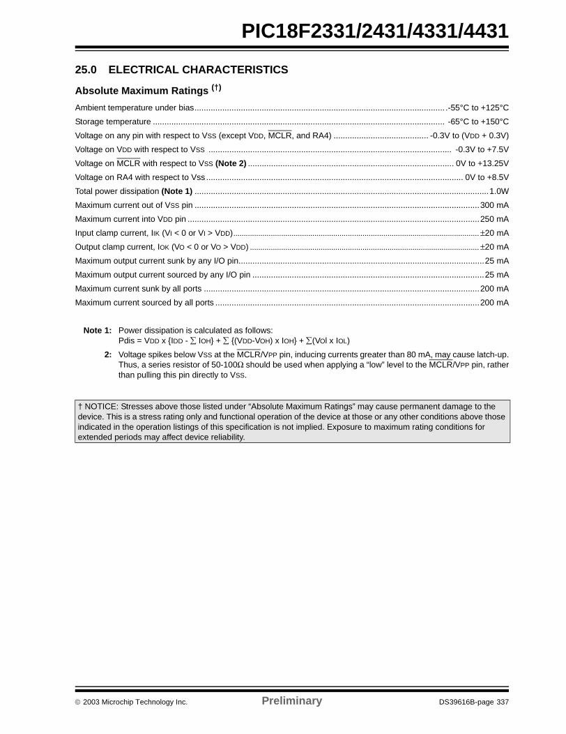
PIC18F2331/2431/4331/4431
25.0 ELECTRICAL CHARACTERISTICS
Absolute Maximum Ratings (†)
Ambient temperature under bias............................................................................................................ .-55°C to +125°C
Storage temperature .............................................................................................................................. -65°C to +150°C
Voltage on any pin with respect to VSS (except VDD, MCLR, and RA4) ......................................... -0.3V to (VDD + 0.3V)
Voltage on VDD with respect to VSS ......................................................................................................... -0.3V to +7.5V
Voltage on MCLR with respect to VSS (Note 2) ......................................................................................... 0V to +13.25V
Voltage on RA4 with respect to Vss ............................................................................................................... 0V to +8.5V
Total power dissipation (Note 1) ...............................................................................................................................1.0W
Maximum current out of VSS pin ...........................................................................................................................300 mA
Maximum current into VDD pin ..............................................................................................................................250 mA
Input clamp current, IIK (VI < 0 or VI > VDD)...................................................................................................................... ±20 mA
Output clamp current, IOK (VO < 0 or VO > VDD) .............................................................................................................. ±20 mA
Maximum output current sunk by any I/O pin..........................................................................................................25 mA
Maximum output current sourced by any I/O pin ....................................................................................................25 mA
Maximum current sunk by all ports .......................................................................................................................200 mA
Maximum current sourced by all ports ..................................................................................................................200 mA
Note 1: Power dissipation is calculated as follows: Pdis = VDD x IDD - ∑ IOH + ∑ (VDD-VOH) x IOH + ∑(VOl x IOL)
2: Voltage spikes below VSS at the MCLR/VPP pin, inducing currents greater than 80 mA, may cause latch-up.Thus, a series resistor of 50-100Ω should be used when applying a “low” level to the MCLR/VPP pin, ratherthan pulling this pin directly to VSS.
† NOTICE: Stresses above those listed under “Absolute Maximum Ratings” may cause permanent damage to the device. This is a stress rating only and functional operation of the device at those or any other conditions above those indicated in the operation listings of this specification is not implied. Exposure to maximum rating conditions for extended periods may affect device reliability.
2003 Microchip Technology Inc. Preliminary DS39616B-page 337

PIC18F2331/2431/4331/4431
FIGURE 25-1: PIC18F2331/2431/4331/4431 VOLTAGE-FREQUENCY GRAPH (INDUSTRIAL)
FIGURE 25-2: PIC18LF2331/2431/4331/4431 VOLTAGE-FREQUENCY GRAPH (INDUSTRIAL)
Frequency
Vo
ltag
e6.0V
5.5V
4.5V
4.0V
2.0V
40 MHz
5.0V
3.5V
3.0V
2.5V
PIC18F2X31/4X31
4.2V
Frequency
Vo
ltag
e
6.0V
5.5V
4.5V
4.0V
2.0V
40 MHz
5.0V
3.5V
3.0V
2.5V
PIC18LF2X31/4X31
FMAX = (16.36 MHz/V) (VDDAPPMIN – 2.0V) + 4 MHz
Note: VDDAPPMIN is the minimum voltage of the PICmicro® device in the application.
4 MHz
4.2V
DS39616B-page 338 Preliminary 2003 Microchip Technology Inc.

PIC18F2331/2431/4331/4431
25.1 DC Characteristics: Supply VoltagePIC18F2331/2431/4331/4431 (Industrial, Extended) PIC18LF2331/2431/4331/4431 (Industrial)
PIC18F2331/2431/4331/4431 (Industrial, Extended)
Standard Operating Conditions (unless otherwise stated)Operating temperature -40°C ≤ TA ≤ +85°C for industrial
PIC18LF2331/2431/4331/4431 (Industrial)
Standard Operating Conditions (unless otherwise stated)Operating temperature -40°C ≤ TA ≤ +85°C for industrial
Param No.
Symbol Characteristic Min Typ Max Units Conditions
VDD Supply Voltage
D001 PIC18LF2X31/4X31 2.0 — 5.5 V HS, XT, RC and LP Osc mode
PIC18F2X31/4X31 4.2 — 5.5 V
D002 VDR RAM Data RetentionVoltage(1)
1.5 — — V
D003 VPOR VDD Start Voltage to ensure internal Power-on Reset signal
— — 0.7 V See section on Power-on Reset for details
D004 SVDD VDD Rise Rateto ensure internal Power-on Reset signal
0.05 — — V/ms See section on Power-on Reset for details
VBOR Brown-out Reset Voltage
D005 BORV1:BORV0 = 10 2.45 — 2.99 V
BORV1:BORV0 = 01 3.80 — 4.64 V
BORV1:BORV0 = 00 4.09 — 4.99 V
Legend: Shading of rows is to assist in readability of the table.Note 1: This is the limit to which VDD can be lowered in Sleep mode, or during a device Reset, without losing RAM data.
2003 Microchip Technology Inc. Preliminary DS39616B-page 339

PIC18F2331/2431/4331/4431
25.2 DC Characteristics: Power-Down and Supply CurrentPIC18F2331/2431/4331/4431 (Industrial, Extended) PIC18LF2331/2431/4331/4431 (Industrial)
PIC18F2331/2431/4331/4431 (Industrial, Extended)
Standard Operating Conditions (unless otherwise stated)Operating temperature -40°C ≤ TA ≤ +85°C for industrial
PIC18LF2331/2431/4331/4431 (Industrial)
Standard Operating Conditions (unless otherwise stated)Operating temperature -40°C ≤ TA ≤ +85°C for industrial
Param No.
Device Typ Max Units Conditions
Power-down Current (IPD)(1)
PIC18LF2X31/4X31 0.1 0.5 µA -40°CVDD = 2.0V,
(Sleep mode)0.1 0.5 µA 25°C
0.2 1.9 µA 85°C
PIC18LF2X31/4X31 0.1 0.5 µA -40°CVDD = 3.0V,
(Sleep mode)0.1 0.5 µA 25°C
0.3 1.9 µA 85°C
All devices 0.1 2.0 µA -40°CVDD = 5.0V,
(Sleep mode)0.1 2.0 µA 25°C
0.4 6.5 µA 85°C
Legend: Shading of rows is to assist in readability of the table.Note 1: The power-down current in Sleep mode does not depend on the oscillator type. Power-down current is measured with
the part in Sleep mode, with all I/O pins in high-impedance state and tied to VDD or VSS, and all features that add delta current disabled (such as WDT, Timer1 Oscillator, BOR, etc.).
2: The supply current is mainly a function of operating voltage, frequency and mode. Other factors, such as I/O pin loading and switching rate, oscillator type and circuit, internal code execution pattern and temperature, also have an impact on the current consumption.The test conditions for all IDD measurements in active Operation mode are:
OSC1 = external square wave, from rail-to-rail; all I/O pins tri-stated, pulled to VDD;MCLR = VDD; WDT enabled/disabled as specified.
3: For RC oscillator configurations, current through REXT is not included. The current through the resistor can be estimated by the formula Ir = VDD/2REXT (mA) with REXT in kΩ.
4: Standard low cost 32 kHz crystals have an operating temperature range of -10°C to +70°C. Extended temperature crystals are available at a much higher cost.
DS39616B-page 340 Preliminary 2003 Microchip Technology Inc.

PIC18F2331/2431/4331/4431
Supply Current (IDD)(2,3)
PIC18LF2X31/4X31 8 40 µA -40°C
FOSC = 31 kHz(RC_RUN mode,
Internal oscillator source)
9 40 µA 25°C VDD = 2.0V
11 40 µA 85°C
PIC18LF2X31/4X31 25 68 µA -40°C
25 68 µA 25°C VDD = 3.0V
20 68 µA 85°C
All devices 55 180 µA -40°C
55 180 µA 25°C VDD = 5.0V
50 180 µA 85°C
PIC18LF2X31/4X31 140 220 µA -40°C
FOSC = 1 MHz(RC_RUN mode,
Internal oscillator source)
145 220 µA 25°C VDD = 2.0V
155 220 µA 85°C
PIC18LF2X31/4X31 215 330 µA -40°C
225 330 µA 25°C VDD = 3.0V
235 330 µA 85°C
All devices 385 550 µA -40°C
390 550 µA 25°C VDD = 5.0V
405 550 µA 85°C
25.2 DC Characteristics: Power-Down and Supply CurrentPIC18F2331/2431/4331/4431 (Industrial, Extended) PIC18LF2331/2431/4331/4431 (Industrial) (Continued)
PIC18F2331/2431/4331/4431 (Industrial, Extended)
Standard Operating Conditions (unless otherwise stated)Operating temperature -40°C ≤ TA ≤ +85°C for industrial
PIC18LF2331/2431/4331/4431 (Industrial)
Standard Operating Conditions (unless otherwise stated)Operating temperature -40°C ≤ TA ≤ +85°C for industrial
Param No.
Device Typ Max Units Conditions
Legend: Shading of rows is to assist in readability of the table.Note 1: The power-down current in Sleep mode does not depend on the oscillator type. Power-down current is measured with
the part in Sleep mode, with all I/O pins in high-impedance state and tied to VDD or VSS, and all features that add delta current disabled (such as WDT, Timer1 Oscillator, BOR, etc.).
2: The supply current is mainly a function of operating voltage, frequency and mode. Other factors, such as I/O pin loading and switching rate, oscillator type and circuit, internal code execution pattern and temperature, also have an impact on the current consumption.The test conditions for all IDD measurements in active Operation mode are:
OSC1 = external square wave, from rail-to-rail; all I/O pins tri-stated, pulled to VDD;MCLR = VDD; WDT enabled/disabled as specified.
3: For RC oscillator configurations, current through REXT is not included. The current through the resistor can be estimated by the formula Ir = VDD/2REXT (mA) with REXT in kΩ.
4: Standard low cost 32 kHz crystals have an operating temperature range of -10°C to +70°C. Extended temperature crystals are available at a much higher cost.
2003 Microchip Technology Inc. Preliminary DS39616B-page 341

PIC18F2331/2431/4331/4431
PIC18LF2X31/4X31 410 600 µA -40°C
FOSC = 4 MHz(RC_RUN mode,
Internal oscillator source)
425 600 µA 25°C VDD = 2.0V
435 600 µA 85°C
PIC18LF2X31/4X31 650 900 µA -40°C
670 900 µA 25°C VDD = 3.0V
680 900 µA 85°C
All devices 1.2 1.8 mA -40°C
1.2 1.8 mA 25°C VDD = 5.0V
1.2 1.8 mA 85°C
25.2 DC Characteristics: Power-Down and Supply CurrentPIC18F2331/2431/4331/4431 (Industrial, Extended) PIC18LF2331/2431/4331/4431 (Industrial) (Continued)
PIC18F2331/2431/4331/4431 (Industrial, Extended)
Standard Operating Conditions (unless otherwise stated)Operating temperature -40°C ≤ TA ≤ +85°C for industrial
PIC18LF2331/2431/4331/4431 (Industrial)
Standard Operating Conditions (unless otherwise stated)Operating temperature -40°C ≤ TA ≤ +85°C for industrial
Param No.
Device Typ Max Units Conditions
Legend: Shading of rows is to assist in readability of the table.Note 1: The power-down current in Sleep mode does not depend on the oscillator type. Power-down current is measured with
the part in Sleep mode, with all I/O pins in high-impedance state and tied to VDD or VSS, and all features that add delta current disabled (such as WDT, Timer1 Oscillator, BOR, etc.).
2: The supply current is mainly a function of operating voltage, frequency and mode. Other factors, such as I/O pin loading and switching rate, oscillator type and circuit, internal code execution pattern and temperature, also have an impact on the current consumption.The test conditions for all IDD measurements in active Operation mode are:
OSC1 = external square wave, from rail-to-rail; all I/O pins tri-stated, pulled to VDD;MCLR = VDD; WDT enabled/disabled as specified.
3: For RC oscillator configurations, current through REXT is not included. The current through the resistor can be estimated by the formula Ir = VDD/2REXT (mA) with REXT in kΩ.
4: Standard low cost 32 kHz crystals have an operating temperature range of -10°C to +70°C. Extended temperature crystals are available at a much higher cost.
DS39616B-page 342 Preliminary 2003 Microchip Technology Inc.

PIC18F2331/2431/4331/4431
Supply Current (IDD)(2,3)
PIC18LF2X31/4X31 4.7 8 µA -40°C
FOSC = 31 kHz(RC_IDLE mode,
Internal oscillator source)
5.0 8 µA 25°C VDD = 2.0V
5.8 11 µA 85°C
PIC18LF2X31/4X31 7.0 11 µA -40°C
7.8 11 µA 25°C VDD = 3.0V
8.7 15 µA 85°C
All devices 12 16 µA -40°C
14 16 µA 25°C VDD = 5.0V
14 22 µA 85°C
PIC18LF2X31/4X31 75 150 µA -40°C
FOSC = 1 MHz(RC_IDLE mode,
Internal oscillator source)
85 150 µA 25°C VDD = 2.0V
95 150 µA 85°C
PIC18LF2X31/4X31 110 180 µA -40°C
125 180 µA 25°C VDD = 3.0V
135 180 µA 85°C
All devices 180 300 µA -40°C
195 300 µA 25°C VDD = 5.0V
200 300 µA 85°C
25.2 DC Characteristics: Power-Down and Supply CurrentPIC18F2331/2431/4331/4431 (Industrial, Extended) PIC18LF2331/2431/4331/4431 (Industrial) (Continued)
PIC18F2331/2431/4331/4431 (Industrial, Extended)
Standard Operating Conditions (unless otherwise stated)Operating temperature -40°C ≤ TA ≤ +85°C for industrial
PIC18LF2331/2431/4331/4431 (Industrial)
Standard Operating Conditions (unless otherwise stated)Operating temperature -40°C ≤ TA ≤ +85°C for industrial
Param No.
Device Typ Max Units Conditions
Legend: Shading of rows is to assist in readability of the table.Note 1: The power-down current in Sleep mode does not depend on the oscillator type. Power-down current is measured with
the part in Sleep mode, with all I/O pins in high-impedance state and tied to VDD or VSS, and all features that add delta current disabled (such as WDT, Timer1 Oscillator, BOR, etc.).
2: The supply current is mainly a function of operating voltage, frequency and mode. Other factors, such as I/O pin loading and switching rate, oscillator type and circuit, internal code execution pattern and temperature, also have an impact on the current consumption.The test conditions for all IDD measurements in active Operation mode are:
OSC1 = external square wave, from rail-to-rail; all I/O pins tri-stated, pulled to VDD;MCLR = VDD; WDT enabled/disabled as specified.
3: For RC oscillator configurations, current through REXT is not included. The current through the resistor can be estimated by the formula Ir = VDD/2REXT (mA) with REXT in kΩ.
4: Standard low cost 32 kHz crystals have an operating temperature range of -10°C to +70°C. Extended temperature crystals are available at a much higher cost.
2003 Microchip Technology Inc. Preliminary DS39616B-page 343

PIC18F2331/2431/4331/4431
PIC18LF2X31/4X31 175 275 µA -40°C
FOSC = 4 MHz(RC_IDLE mode,
Internal oscillator source)
185 275 µA 25°C VDD = 2.0V
195 275 µA 85°C
PIC18LF2X31/4X31 265 375 µA -40°C
280 375 µA 25°C VDD = 3.0V
300 375 µA 85°C
All devices 475 800 µA -40°C
500 800 µA 25°C VDD = 5.0V
505 800 µA 85°C
25.2 DC Characteristics: Power-Down and Supply CurrentPIC18F2331/2431/4331/4431 (Industrial, Extended) PIC18LF2331/2431/4331/4431 (Industrial) (Continued)
PIC18F2331/2431/4331/4431 (Industrial, Extended)
Standard Operating Conditions (unless otherwise stated)Operating temperature -40°C ≤ TA ≤ +85°C for industrial
PIC18LF2331/2431/4331/4431 (Industrial)
Standard Operating Conditions (unless otherwise stated)Operating temperature -40°C ≤ TA ≤ +85°C for industrial
Param No.
Device Typ Max Units Conditions
Legend: Shading of rows is to assist in readability of the table.Note 1: The power-down current in Sleep mode does not depend on the oscillator type. Power-down current is measured with
the part in Sleep mode, with all I/O pins in high-impedance state and tied to VDD or VSS, and all features that add delta current disabled (such as WDT, Timer1 Oscillator, BOR, etc.).
2: The supply current is mainly a function of operating voltage, frequency and mode. Other factors, such as I/O pin loading and switching rate, oscillator type and circuit, internal code execution pattern and temperature, also have an impact on the current consumption.The test conditions for all IDD measurements in active Operation mode are:
OSC1 = external square wave, from rail-to-rail; all I/O pins tri-stated, pulled to VDD;MCLR = VDD; WDT enabled/disabled as specified.
3: For RC oscillator configurations, current through REXT is not included. The current through the resistor can be estimated by the formula Ir = VDD/2REXT (mA) with REXT in kΩ.
4: Standard low cost 32 kHz crystals have an operating temperature range of -10°C to +70°C. Extended temperature crystals are available at a much higher cost.
DS39616B-page 344 Preliminary 2003 Microchip Technology Inc.

PIC18F2331/2431/4331/4431
Supply Current (IDD)(2,3)
PIC18LF2X31/4X31 150 250 µA -40°C
FOSC = 1 MHZ
(PRI_RUN,EC oscillator)
150 250 µA 25°C VDD = 2.0V
160 250 µA 85°C
PIC18LF2X31/4X31 340 350 µA -40°C
300 350 µA 25°C VDD = 3.0V
280 350 µA 85°C
All devices 0.72 1.0 mA -40°C
0.63 1.0 mA 25°C VDD = 5.0V
0.57 1.0 mA 85°C
PIC18LF2X31/4X31 440 600 µA -40°C
FOSC = 4 MHz(PRI_RUN,
EC oscillator)
450 600 µA 25°C VDD = 2.0V
460 600 µA 85°C
PIC18LF2X31/4X31 0.80 1.0 mA -40°C
0.78 1.0 mA 25°C VDD = 3.0V
0.77 1.0 mA 85°C
All devices 1.6 2.0 mA -40°C
1.5 2.0 mA 25°C VDD = 5.0V
1.5 2.0 mA 85°C
All devices 9.5 12 mA -40°C
FOSC = 40 MHZ
(PRI_RUN,EC oscillator)
9.7 12 mA 25°C VDD = 4.2V
9.9 12 mA 85°C
All devices 11.9 15 mA -40°C
12.1 15 mA 25°C VDD = 5.0V
12.3 15 mA 85°C
25.2 DC Characteristics: Power-Down and Supply CurrentPIC18F2331/2431/4331/4431 (Industrial, Extended) PIC18LF2331/2431/4331/4431 (Industrial) (Continued)
PIC18F2331/2431/4331/4431 (Industrial, Extended)
Standard Operating Conditions (unless otherwise stated)Operating temperature -40°C ≤ TA ≤ +85°C for industrial
PIC18LF2331/2431/4331/4431 (Industrial)
Standard Operating Conditions (unless otherwise stated)Operating temperature -40°C ≤ TA ≤ +85°C for industrial
Param No.
Device Typ Max Units Conditions
Legend: Shading of rows is to assist in readability of the table.Note 1: The power-down current in Sleep mode does not depend on the oscillator type. Power-down current is measured with
the part in Sleep mode, with all I/O pins in high-impedance state and tied to VDD or VSS, and all features that add delta current disabled (such as WDT, Timer1 Oscillator, BOR, etc.).
2: The supply current is mainly a function of operating voltage, frequency and mode. Other factors, such as I/O pin loading and switching rate, oscillator type and circuit, internal code execution pattern and temperature, also have an impact on the current consumption.The test conditions for all IDD measurements in active Operation mode are:
OSC1 = external square wave, from rail-to-rail; all I/O pins tri-stated, pulled to VDD;MCLR = VDD; WDT enabled/disabled as specified.
3: For RC oscillator configurations, current through REXT is not included. The current through the resistor can be estimated by the formula Ir = VDD/2REXT (mA) with REXT in kΩ.
4: Standard low cost 32 kHz crystals have an operating temperature range of -10°C to +70°C. Extended temperature crystals are available at a much higher cost.
2003 Microchip Technology Inc. Preliminary DS39616B-page 345

PIC18F2331/2431/4331/4431
Supply Current (IDD)(2,3)
PIC18LF2X31/4X31 35 50 µA -40°C
FOSC = 1 MHz(PRI_IDLE mode,
EC oscillator)
35 50 µA 25°C VDD = 2.0V
35 60 µA 85°C
PIC18LF2X31/4X31 55 80 µA -40°C
50 80 µA 25°C VDD = 3.0V
60 100 µA 85°C
All devices 105 150 µA -40°C
110 150 µA 25°C VDD = 5.0V
115 150 µA 85°C
PIC18LF2X31/4X31 135 180 µA -40°C
FOSC = 4 MHz(PRI_IDLE mode,
EC oscillator)
140 180 µA 25°C VDD = 2.0V
140 180 µA 85°C
PIC18LF2X31/4X31 215 280 µA -40°C
225 280 µA 25°C VDD = 3.0V
230 280 µA 85°C
All devices 410 525 µA -40°C
420 525 µA 25°C VDD = 5.0V
430 525 µA 85°C
All devices 3.2 4.1 mA -40°C
FOSC = 40 MHz(PRI_IDLE mode,
EC oscillator)
3.2 4.1 mA 25°C VDD = 4.2 V
3.3 4.1 mA 85°C
All devices 4.0 5.1 mA -40°C
4.1 5.1 mA 25°C VDD = 5.0V
4.1 5.1 mA 85°C
25.2 DC Characteristics: Power-Down and Supply CurrentPIC18F2331/2431/4331/4431 (Industrial, Extended) PIC18LF2331/2431/4331/4431 (Industrial) (Continued)
PIC18F2331/2431/4331/4431 (Industrial, Extended)
Standard Operating Conditions (unless otherwise stated)Operating temperature -40°C ≤ TA ≤ +85°C for industrial
PIC18LF2331/2431/4331/4431 (Industrial)
Standard Operating Conditions (unless otherwise stated)Operating temperature -40°C ≤ TA ≤ +85°C for industrial
Param No.
Device Typ Max Units Conditions
Legend: Shading of rows is to assist in readability of the table.Note 1: The power-down current in Sleep mode does not depend on the oscillator type. Power-down current is measured with
the part in Sleep mode, with all I/O pins in high-impedance state and tied to VDD or VSS, and all features that add delta current disabled (such as WDT, Timer1 Oscillator, BOR, etc.).
2: The supply current is mainly a function of operating voltage, frequency and mode. Other factors, such as I/O pin loading and switching rate, oscillator type and circuit, internal code execution pattern and temperature, also have an impact on the current consumption.The test conditions for all IDD measurements in active Operation mode are:
OSC1 = external square wave, from rail-to-rail; all I/O pins tri-stated, pulled to VDD;MCLR = VDD; WDT enabled/disabled as specified.
3: For RC oscillator configurations, current through REXT is not included. The current through the resistor can be estimated by the formula Ir = VDD/2REXT (mA) with REXT in kΩ.
4: Standard low cost 32 kHz crystals have an operating temperature range of -10°C to +70°C. Extended temperature crystals are available at a much higher cost.
DS39616B-page 346 Preliminary 2003 Microchip Technology Inc.

PIC18F2331/2431/4331/4431
Supply Current (IDD)(2,3)
PIC18LF2X31/4X31 5.1 9 µA -10°C
FOSC = 32 kHz(4)
(SEC_RUN mode, Timer1 as clock)
5.8 9 µA 25°C VDD = 2.0V
7.9 11 µA 70°C
PIC18LF2X31/4X31 7.9 12 µA -10°C
8.9 12 µA 25°C VDD = 3.0V
10.5 14 µA 70°C
All devices 12.5 20 µA -10°C
16.3 20 µA 25°C VDD = 5.0V
18.9 25 µA 70°C
Supply Current (IDD)(2,3)
PIC18LF2X31/4X31 9.2 15 µA -10°C
FOSC = 32 kHz(4)
(SEC_IDLE mode, Timer1 as clock)
9.6 15 µA 25°C VDD = 2.0V
12.7 18 µA 70°C
PIC18LF2X31/4X31 22.0 30 µA -10°C
21.0 30 µA 25°C VDD = 3.0V
20.0 35 µA 70°C
All devices 30 80 µA -10°C
45 80 µA 25°C VDD = 5.0V
45 85 µA 70°C
25.2 DC Characteristics: Power-Down and Supply CurrentPIC18F2331/2431/4331/4431 (Industrial, Extended) PIC18LF2331/2431/4331/4431 (Industrial) (Continued)
PIC18F2331/2431/4331/4431 (Industrial, Extended)
Standard Operating Conditions (unless otherwise stated)Operating temperature -40°C ≤ TA ≤ +85°C for industrial
PIC18LF2331/2431/4331/4431 (Industrial)
Standard Operating Conditions (unless otherwise stated)Operating temperature -40°C ≤ TA ≤ +85°C for industrial
Param No.
Device Typ Max Units Conditions
Legend: Shading of rows is to assist in readability of the table.Note 1: The power-down current in Sleep mode does not depend on the oscillator type. Power-down current is measured with
the part in Sleep mode, with all I/O pins in high-impedance state and tied to VDD or VSS, and all features that add delta current disabled (such as WDT, Timer1 Oscillator, BOR, etc.).
2: The supply current is mainly a function of operating voltage, frequency and mode. Other factors, such as I/O pin loading and switching rate, oscillator type and circuit, internal code execution pattern and temperature, also have an impact on the current consumption.The test conditions for all IDD measurements in active Operation mode are:
OSC1 = external square wave, from rail-to-rail; all I/O pins tri-stated, pulled to VDD;MCLR = VDD; WDT enabled/disabled as specified.
3: For RC oscillator configurations, current through REXT is not included. The current through the resistor can be estimated by the formula Ir = VDD/2REXT (mA) with REXT in kΩ.
4: Standard low cost 32 kHz crystals have an operating temperature range of -10°C to +70°C. Extended temperature crystals are available at a much higher cost.
2003 Microchip Technology Inc. Preliminary DS39616B-page 347

PIC18F2331/2431/4331/4431
Module Differential Currents (∆IWDT, ∆IBOR, ∆ILVD, ∆IOSCB, ∆IAD)
D022(∆IWDT)
Watchdog Timer 1.5 4.0 µA -40°C
2.2 4.0 µA 25°C VDD = 2.0V
3.1 5.0 µA 85°C
2.5 6.0 µA -40°C
3.3 6.0 µA 25°C VDD = 3.0V
4.7 7.0 µA 85°C
3.7 10.0 µA -40°C
4.5 10.0 µA 25°C VDD = 5.0V
6.1 13.0 µA 85°C
D022A Brown-out Reset 19 35.0 µA -40°C to +85°C VDD = 3.0V
(∆IBOR) 24 45.0 µA -40°C to +85°C VDD = 5.0V
D022B Low-Voltage Detect 8.5 25.0 µA -40°C to +85°C VDD = 2.0V
(∆ILVD) 16 35.0 µA -40°C to +85°C VDD = 3.0V
20 45.0 µA -40°C to +85°C VDD = 5.0V
D025 Timer1 Oscillator 1.7 3.5 µA -40°C
(∆IOSCB) 1.8 3.5 µA 25°C VDD = 2.0V 32 kHz on Timer1(4)
2.1 4.5 µA 85°C
2.2 4.5 µA -40°C
2.6 4.5 µA 25°C VDD = 3.0V 32 kHz on Timer1(4)
2.8 5.5 µA 85°C
3.0 6.0 µA -40°C
3.3 6.0 µA 25°C VDD = 5.0V 32 kHz on Timer1(4)
3.6 7.0 µA 85°C
D026(∆IAD)
A/D Converter 1.0 3.0 µA -40°C to 85°C VDD = 2.0V
1.0 4.0 µA -40°C to 85°C VDD = 3.0V A/D on, not converting
2.0 10.0 µA -40°C to 85°C VDD = 5.0V
25.2 DC Characteristics: Power-Down and Supply CurrentPIC18F2331/2431/4331/4431 (Industrial, Extended) PIC18LF2331/2431/4331/4431 (Industrial) (Continued)
PIC18F2331/2431/4331/4431 (Industrial, Extended)
Standard Operating Conditions (unless otherwise stated)Operating temperature -40°C ≤ TA ≤ +85°C for industrial
PIC18LF2331/2431/4331/4431 (Industrial)
Standard Operating Conditions (unless otherwise stated)Operating temperature -40°C ≤ TA ≤ +85°C for industrial
Param No.
Device Typ Max Units Conditions
Legend: Shading of rows is to assist in readability of the table.Note 1: The power-down current in Sleep mode does not depend on the oscillator type. Power-down current is measured with
the part in Sleep mode, with all I/O pins in high-impedance state and tied to VDD or VSS, and all features that add delta current disabled (such as WDT, Timer1 Oscillator, BOR, etc.).
2: The supply current is mainly a function of operating voltage, frequency and mode. Other factors, such as I/O pin loading and switching rate, oscillator type and circuit, internal code execution pattern and temperature, also have an impact on the current consumption.The test conditions for all IDD measurements in active Operation mode are:
OSC1 = external square wave, from rail-to-rail; all I/O pins tri-stated, pulled to VDD;MCLR = VDD; WDT enabled/disabled as specified.
3: For RC oscillator configurations, current through REXT is not included. The current through the resistor can be estimated by the formula Ir = VDD/2REXT (mA) with REXT in kΩ.
4: Standard low cost 32 kHz crystals have an operating temperature range of -10°C to +70°C. Extended temperature crystals are available at a much higher cost.
DS39616B-page 348 Preliminary 2003 Microchip Technology Inc.

PIC18F2331/2431/4331/4431
25.3 DC Characteristics: PIC18F2331/2431/4331/4431 (Industrial) PIC18LF2331/2431/4331/4431 (Industrial)
DC CHARACTERISTICSStandard Operating Conditions (unless otherwise stated)Operating temperature -40°C ≤ TA ≤ +85°C for industrial
ParamNo.
Symbol Characteristic Min Max Units Conditions
VIL Input Low Voltage
I/O ports:
D030 with TTL buffer VSS 0.15 VDD V VDD < 4.5V
D030A — 0.8 V 4.5V ≤ VDD ≤ 5.5V
D031 with Schmitt Trigger bufferRC3 and RC4
VSS
VSS
0.2 VDD
0.3 VDD
VV
D032 MCLR VSS 0.2 VDD V
D032A OSC1 and T1OSI VSS 0.3 VDD V LP, XT, HS, HSPLL modes(1)
D033 OSC1 VSS 0.2 VDD V EC mode(1)
VIH Input High Voltage
I/O ports:
D040 with TTL buffer 0.25 VDD + 0.8V VDD V VDD < 4.5V
D040A 2.0 VDD V 4.5V ≤ VDD ≤ 5.5V
D041 with Schmitt Trigger bufferRC3 and RC4
0.8 VDD
0.7 VDD
VDD
VDD
VV
D042 MCLR 0.8 VDD VDD V
D042A OSC1 and T1OSI 0.7 VDD VDD V LP, XT, HS, HSPLL modes(1)
D043 OSC1 0.8 VDD VDD V EC mode(1)
IIL Input Leakage Current(2,3)
D060 I/O ports — ±1 µA VSS ≤ VPIN ≤ VDD, Pin at hi-impedance
D061 MCLR — ±1 µA Vss ≤ VPIN ≤ VDD
D063 OSC1 — ±1 µA Vss ≤ VPIN ≤ VDD
IPU Weak Pull-up Current
D070 IPURB PORTB weak pull-up current 50 400 µA VDD = 5V, VPIN = VSS
Note 1: In RC oscillator configuration, the OSC1/CLKI pin is a Schmitt Trigger input. It is not recommended that the PICmicro device be driven with an external clock while in RC mode.
2: The leakage current on the MCLR pin is strongly dependent on the applied voltage level. The specified levels represent normal operating conditions. Higher leakage current may be measured at different input voltages.
3: Negative current is defined as current sourced by the pin.4: Parameter is characterized but not tested.
2003 Microchip Technology Inc. Preliminary DS39616B-page 349

PIC18F2331/2431/4331/4431
VOL Output Low Voltage
D080 I/O ports — 0.6 V IOL = 8.5 mA, VDD = 4.5V, -40°C to +85°C
D083 OSC2/CLKO(RC, RCIO, EC, ECIO modes)
— 0.6 V IOL = 1.6 mA, VDD = 4.5V, -40°C to +85°C
VOH Output High Voltage(3)
D090 I/O ports VDD – 0.7 — V IOH = -3.0 mA, VDD = 4.5V,-40°C to +85°C
D092 OSC2/CLKO (RC, RCIO, EC, ECIO modes)
VDD – 0.7 — V IOH = -1.3 mA, VDD = 4.5V,-40°C to +85°C
D150 VOD Open-Drain High Voltage — 8.5 V RA4 pin
Capacitive Loading Specson Output Pins
D100(4) COSC2 OSC2 pin — 15 pF In XT, HS and LP modes when external clock is used to drive OSC1
D101 CIO All I/O pins and OSC2 (in RC mode)
— 50 pF To meet the AC Timing Specifications
D102 CB SCL, SDA — 400 pF I2C™ Specification
25.3 DC Characteristics: PIC18F2331/2431/4331/4431 (Industrial) PIC18LF2331/2431/4331/4431 (Industrial) (Continued)
DC CHARACTERISTICSStandard Operating Conditions (unless otherwise stated)Operating temperature -40°C ≤ TA ≤ +85°C for industrial
ParamNo.
Symbol Characteristic Min Max Units Conditions
Note 1: In RC oscillator configuration, the OSC1/CLKI pin is a Schmitt Trigger input. It is not recommended that the PICmicro device be driven with an external clock while in RC mode.
2: The leakage current on the MCLR pin is strongly dependent on the applied voltage level. The specified levels represent normal operating conditions. Higher leakage current may be measured at different input voltages.
3: Negative current is defined as current sourced by the pin.4: Parameter is characterized but not tested.
DS39616B-page 350 Preliminary 2003 Microchip Technology Inc.

PIC18F2331/2431/4331/4431
TABLE 25-1: MEMORY PROGRAMMING REQUIREMENTS
DC CharacteristicsStandard Operating Conditions (unless otherwise stated)Operating temperature -40°C ≤ TA ≤ +85°C for industrial
ParamNo.
Sym Characteristic Min Typ† Max Units Conditions
Internal Program Memory Programming Specifications(1)
D110 VPP Voltage on MCLR/VPP pin 9.00 — 13.25 V (Note 3)
D112 IPP Current into MCLR/VPP pin — — 300 µA
D113 IDDP Supply Current during Programming
— — 1 mA
Data EEPROM Memory
D120 ED Byte Endurance 100K 1M — E/W -40°C to +85°CD121 VDRW VDD for Read/Write VMIN — 5.5 V Using EECON to read/write
VMIN = Minimum operating voltage
D122 TDEW Erase/Write Cycle Time — 4 — ms
D123 TRETD Characteristic Retention 40 — — Year Provided no other specifications are violated
D124 TREF Number of Total Erase/Write Cycles before Refresh(2)
1M 10M — E/W -40°C to +85°C
Program Flash Memory
D130 EP Cell Endurance 10K 100K — E/W -40°C to +85°CD131 VPR VDD for Read VMIN — 5.5 V VMIN = Minimum operating
voltage
D132 VIE VDD for Block Erase 4.5 — 5.5 V Using ICSP port
D132A VIW VDD for Externally Timed Erase or Write
4.5 — 5.5 V Using ICSP port
D132B VPEW VDD for Self-timed Write VMIN — 5.5 V VMIN = Minimum operating voltage
D133 TIE ICSP Block Erase Cycle Time — 4 — ms VDD > 4.5V
D133A TIW ICSP Erase or Write Cycle Time (externally timed)
1 — — ms VDD > 4.5V
D133A TIW Self-timed Write Cycle Time — 2 — ms
D134 TRETD Characteristic Retention 40 100 — Year Provided no other specifications are violated
† Data in “Typ” column is at 5.0V, 25°C unless otherwise stated. These parameters are for design guidance only and are not tested.
Note 1: These specifications are for programming the on-chip program memory through the use of Table Write instructions.
2: Refer to Section 7.8 “Using the Data EEPROM” for a more detailed discussion on data EEPROM endurance.
3: Required only if low-voltage programming is disabled.
2003 Microchip Technology Inc. Preliminary DS39616B-page 351

PIC18F2331/2431/4331/4431
FIGURE 25-3: LOW-VOLTAGE DETECT CHARACTERISTICS
TABLE 25-2: LOW-VOLTAGE DETECT CHARACTERISTICS
VLVD
LVDIF
VDD
(LVDIF set by hardware)
(LVDIF can be cleared in software)
Standard Operating Conditions (unless otherwise stated)Operating temperature -40°C ≤ TA ≤ +85°C for industrial
Param No.
Symbol Characteristic Min Typ† Max Units Conditions
D420 LVD Voltage on VDD Transition High to Low
LVV = 0010 2.08 2.26 2.44 V
LVV = 0011 2.26 2.45 2.65 V
LVV = 0100 2.35 2.55 2.76 V
LVV = 0101 2.55 2.77 2.99 V
LVV = 0110 2.64 2.87 3.10 V
LVV = 0111 2.82 3.07 3.31 V
LVV = 1000 3.09 3.36 3.63 V
LVV = 1001 3.29 3.57 3.86 V
LVV = 1010 3.38 3.67 3.96 V
LVV = 1011 3.56 3.87 4.18 V
LVV = 1100 3.75 4.07 4.40 V
LVV = 1101 3.93 4.28 4.62 V
LVV = 1110 4.23 4.60 4.96 V
† Production tested at TAMB = 25°C. Specifications over temp. limits ensured by characterization.
DS39616B-page 352 Preliminary 2003 Microchip Technology Inc.

PIC18F2331/2431/4331/4431
25.4 AC (Timing) Characteristics
25.4.1 TIMING PARAMETER SYMBOLOGY
The timing parameter symbols have been createdfollowing one of the following formats:
1. TppS2ppS 3. TCC:ST (I2C specifications only)
2. TppS 4. Ts (I2C specifications only)T
F Frequency T Time
Lowercase letters (pp) and their meanings:pp
cc CCP1 osc OSC1
ck CLKO rd RDcs CS rw RD or WRdi SDI sc SCK
do SDO ss SSdt Data in t0 T0CKIio I/O port t1 T1CKI
mc MCLR wr WRUppercase letters and their meanings:S
F Fall P PeriodH High R RiseI Invalid (Hi-impedance) V Valid
L Low Z Hi-impedanceI2C only
AA output access High High
BUF Bus free Low LowTCC:ST (I2C specifications only)CC
HD Hold SU SetupST
DAT DATA input hold STO Stop condition
STA Start condition
2003 Microchip Technology Inc. Preliminary DS39616B-page 353

PIC18F2331/2431/4331/4431
25.4.2 TIMING CONDITIONS
The temperature and voltages specified in Table 25-3apply to all timing specifications unless otherwisenoted. Figure 25-4 specifies the load conditions for thetiming specifications.
TABLE 25-3: TEMPERATURE AND VOLTAGE SPECIFICATIONS - AC
FIGURE 25-4: LOAD CONDITIONS FOR DEVICE TIMING SPECIFICATIONS
Note: Because of space limitations, the genericterms “PIC18FXX31” and “PIC18LFXX31”are used throughout this section to refer tothe PIC18F2331/2431/4331/4431 andPIC18LF2331/2431/4331/4431 families ofdevices specifically, and only thosedevices.
AC CHARACTERISTICS
Standard Operating Conditions (unless otherwise stated)Operating temperature -40°C ≤ TA ≤ +85°C for industrialOperating voltage VDD range as described in DC spec Section 25.1 and Section 25.3. LF parts operate for industrial temperatures only.
VDD/2
CL
RL
Pin
Pin
VSS
VSS
CL
RL = 464Ω
CL = 50 pF for all pins except OSC2/CLKOand including D and E outputs as ports
Load Condition 1 Load Condition 2
DS39616B-page 354 Preliminary 2003 Microchip Technology Inc.

PIC18F2331/2431/4331/4431
25.4.3 TIMING DIAGRAMS AND SPECIFICATIONS
FIGURE 25-5: EXTERNAL CLOCK TIMING (ALL MODES EXCEPT PLL)
TABLE 25-4: EXTERNAL CLOCK TIMING REQUIREMENTS
OSC1
CLKO
Q4 Q1 Q2 Q3 Q4 Q1
1
2
3 3 4 4
Param.No.
Symbol Characteristic Min Max Units Conditions
1A FOSC External CLKI Frequency(1) DC 40 MHz EC, ECIO
Oscillator Frequency(1) DC 4 MHz RC osc 0.1 4 MHz XT osc 4 25 MHz HS osc
4 10 MHz HS + PLL osc5 200 kHz LP Osc mode
1 TOSC External CLKI Period(1) 25 — ns EC, ECIO
Oscillator Period(1) 250 — ns RC osc 250 10,000 ns XT osc
25100
250250
nsns
HS osc HS + PLL osc
25 — µs LP osc
2 TCY Instruction Cycle Time(1) 100 — ns TCY = 4/FOSC 3 TosL,
TosHExternal Clock in (OSC1) High or Low Time
30 — ns XT osc2.5 — µs LP osc
10 — ns HS osc4 TosR,
TosFExternal Clock in (OSC1) Rise or Fall Time
— 20 ns XT osc— 50 ns LP osc
— 7.5 ns HS oscNote 1: Instruction cycle period (TCY) equals four times the input oscillator time base period for all configurations
except PLL. All specified values are based on characterization data for that particular oscillator type under standard operating conditions with the device executing code. Exceeding these specified limits may result in an unstable oscillator operation and/or higher than expected current consumption. All devices are tested to operate at “min.” values with an external clock applied to the OSC1/CLKI pin. When an external clock input is used, the “max.” cycle time limit is “DC” (no clock) for all devices.
2003 Microchip Technology Inc. Preliminary DS39616B-page 355

PIC18F2331/2431/4331/4431
TABLE 25-5: PLL CLOCK TIMING SPECIFICATIONS (VDD = 4.2V TO 5.5V)Param
No.Sym Characteristic Min Typ† Max Units Conditions
F10 FOSC Oscillator Frequency Range 4 — 10 MHz HS mode only
F11 FSYS On-chip VCO System Frequency 16 — 40 MHz HS mode only
F12 TPLL PLL Start-up Time (Lock Time) — — 2 ms
F13 ∆CLK CLKO Stability (Jitter) -2 — +2 % † Data in “Typ” column is at 5V, 25°C unless otherwise stated. These parameters are for design guidance only
and are not tested.
TABLE 25-6: INTERNAL RC ACCURACYPIC18F2331/2431/4331/4431 (Industrial)PIC18LF2331/2431/4331/4431 (Industrial)
PIC18F1220/1320 (Industrial)
Standard Operating Conditions (unless otherwise stated)Operating temperature -40°C ≤ TA ≤ +85°C for industrial
PIC18LF1220/1320 (Industrial)
Standard Operating Conditions (unless otherwise stated)Operating temperature -40°C ≤ TA ≤ +85°C for industrial
ParamNo.
Device Min Typ Max Units Conditions
INTOSC Accuracy @ Freq = 8 MHz, 4 MHz, 2 MHz, 1 MHz, 500 kHz, 250 kHz, 125 kHz(1)
F2 PIC18LF2331/2431/4331/4431 -15 +/-5 +15 % 25°C VDD = 3.0V
F3 All devices -15 +/-5 +15 % 25°C VDD = 5.0V
INTRC Accuracy @ Freq = 31 kHz(2)
F5 PIC18LF2331/2431/4331/4431 26.562 — 35.938 kHz 25°C VDD = 3.0V
F6 All devices 26.562 — 35.938 kHz 25°C VDD = 5.0V
INTRC Stability(3)
F8 PIC18LF2331/2431/4331/4431 TBD 1 TBD % 25°C VDD = 3.0V
F9 All devices TBD 1 TBD % 25°C VDD = 5.0V
Legend: Shading of rows is to assist in readability of the table.Note 1: Frequency calibrated at 25°C. OSCTUNE register can be used to compensate for temperature drift.
2: INTRC frequency after calibration.3: Change of INTRC frequency as VDD changes.
DS39616B-page 356 Preliminary 2003 Microchip Technology Inc.

PIC18F2331/2431/4331/4431
FIGURE 25-6: CLKO AND I/O TIMING
TABLE 25-7: CLKO AND I/O TIMING REQUIREMENTS
Note: Refer to Figure 25-4 for load conditions.
OSC1
CLKO
I/O Pin(Input)
I/O Pin(Output)
Q4 Q1 Q2 Q3
10
1314
17
20, 21
19 18
15
11
12
16
Old Value New Value
ParamNo.
Symbol Characteristic Min Typ Max Units Conditions
10 TosH2ckL OSC1 ↑ to CLKO ↓ — 75 200 ns (1)
11 TosH2ckH OSC1 ↑ to CLKO ↑ — 75 200 ns (1)
12 TckR CLKO rise time — 35 100 ns (1)
13 TckF CLKO fall time — 35 100 ns (1)
14 TckL2ioV CLKO ↓ to Port out valid — — 0.5 TCY + 20 ns (1)
15 TioV2ckH Port in valid before CLKO ↑ 0.25 TCY + 25 — — ns (1)
16 TckH2ioI Port in hold after CLKO ↑ 0 — — ns (1)
17 TosH2ioV OSC1↑ (Q1 cycle) to Port out valid — 50 150 ns
18 TosH2ioI OSC1↑ (Q2 cycle) to Port input invalid (I/O in hold time)
PIC18FXX31 100 — — ns
18A PIC18LFXX31 200 — — ns
19 TioV2osH Port input valid to OSC1↑ (I/O in setup time) 0 — — ns
20 TioR Port output rise time PIC18FXX31 — 10 25 ns
20A PIC18LFXX31 — — 60 ns
21 TioF Port output fall time PIC18FXX31 — 10 25 ns
21A PIC18LFXX31 — — 60 ns
22†† TINP INT pin high or low time TCY — — ns
23†† TRBP RB7:RB4 change INT high or low time TCY — — ns
24†† TRCP RB7:RB4 change INT high or low time 20 ns
†† These parameters are asynchronous events not related to any internal clock edges.Note 1: Measurements are taken in RC mode, where CLKO output is 4 x TOSC.
2003 Microchip Technology Inc. Preliminary DS39616B-page 357

PIC18F2331/2431/4331/4431
FIGURE 25-7: RESET, WATCHDOG TIMER, OSCILLATOR START-UP TIMER AND POWER-UP TIMER TIMING
FIGURE 25-8: BROWN-OUT RESET TIMING
TABLE 25-8: RESET, WATCHDOG TIMER, OSCILLATOR START-UP TIMER, POWER-UP TIMER AND BROWN-OUT RESET REQUIREMENTS
Param. No.
Symbol Characteristic Min Typ Max Units Conditions
30 TmcL MCLR Pulse Width (low) 2 — — µs31 TWDT Watchdog Timer Time-out Period
(No Postscaler)— 4.00 TBD ms
32 TOST Oscillation Start-up Timer Period 1024 TOSC — 1024 TOSC — TOSC = OSC1 period33 TPWRT Power-up Timer Period — 65.5 TBD ms
34 TIOZ I/O Hi-impedance from MCLR Low or Watchdog Timer Reset
— 2 — µs
35 TBOR Brown-out Reset Pulse Width 200 — — µs VDD ≤ BVDD (see D005)36 TIVRST Time for Internal Reference
Voltage to become stable— 20 50 µs
37 TLVD Low-Voltage Detect Pulse Width 200 — — µs VDD ≤ VLVD
VDD
MCLR
InternalPOR
PWRTTime-out
OSCTime-out
InternalReset
WatchdogTimerReset
33
32
30
3134
I/O Pins
34
Note: Refer to Figure 25-4 for load conditions.
VDDBVDD
35VBGAP = 1.2V
VIRVST
Enable Internal Reference Voltage
Internal Reference Voltage Stable 36
DS39616B-page 358 Preliminary 2003 Microchip Technology Inc.

PIC18F2331/2431/4331/4431
FIGURE 25-9: TIMER0 AND TIMER1 EXTERNAL CLOCK TIMINGS
TABLE 25-9: TIMER0 AND TIMER1 EXTERNAL CLOCK REQUIREMENTS
Note: Refer to Figure 25-4 for load conditions.
46
47
45
48
41
42
40
T0CKI
T1OSO/T1CKI
TMR0 orTMR1
Param No.
Symbol Characteristic Min Max Units Conditions
40 Tt0H T0CKI High Pulse Width No Prescaler 0.5 TCY + 20 — nsWith Prescaler 10 — ns
41 Tt0L T0CKI Low Pulse Width No Prescaler 0.5 TCY + 20 — ns
With Prescaler 10 — ns42 Tt0P T0CKI Period No Prescaler TCY + 10 — ns
With Prescaler Greater of:20 ns or TCY + 40
N
— ns N = prescalevalue (1, 2, 4,..., 256)
45 Tt1H T1CKI High Time
Synchronous, no prescaler 0.5 TCY + 20 — ns
Synchronous,with prescaler
PIC18FXX31 10 — nsPIC18LFXX31 25 — ns
Asynchronous PIC18FXX31 30 — ns
PIC18LFXX31 50 — ns46 Tt1L T1CKI
Low TimeSynchronous, no prescaler 0.5 TCY + 5 — nsSynchronous, with prescaler
PIC18FXX31 10 — ns
PIC18LFXX31 25 — nsAsynchronous PIC18FXX31 30 — ns
PIC18LFXX31 TBD TBD ns
47 Tt1P T1CKI Input Period
Synchronous Greater of:20 ns or TCY + 40
N
— ns N = prescalevalue (1, 2, 4, 8)
Asynchronous 60 — ns
Ft1 T1CKI Oscillator Input Frequency Range DC 50 kHz48 Tcke2tmrI Delay from External T1CKI Clock Edge to
Timer Increment2 TOSC 7 TOSC —
2003 Microchip Technology Inc. Preliminary DS39616B-page 359

PIC18F2331/2431/4331/4431
FIGURE 25-10: CAPTURE/COMPARE/PWM TIMINGS (ALL CCP MODULES)
TABLE 25-10: CAPTURE/COMPARE/PWM REQUIREMENTS (ALL CCP MODULES)
Note: Refer to Figure 25-4 for load conditions.
CCPx(Capture Mode)
50 51
52
CCPx
53 54
(Compare or PWM Mode)
Param No.
Symbol Characteristic Min Max Units Conditions
50 TccL CCPx input low time
No Prescaler 0.5 TCY + 20 — nsWith Prescaler
PIC18FXX31 10 — nsPIC18LFXX31 20 — ns
51 TccH CCPx input high time
No Prescaler 0.5 TCY + 20 — nsWithPrescaler
PIC18FXX31 10 — nsPIC18LFXX31 20 — ns
52 TccP CCPx input period 3 TCY + 40N
— ns N = prescale value (1,4 or 16)
53 TccR CCPx output fall time PIC18FXX31 — 25 nsPIC18LFXX31 — 45 ns
54 TccF CCPx output fall time PIC18FXX31 — 25 ns
PIC18LFXX31 — 45 ns
DS39616B-page 360 Preliminary 2003 Microchip Technology Inc.

PIC18F2331/2431/4331/4431
FIGURE 25-11: EXAMPLE SPI MASTER MODE TIMING (CKE = 0)
TABLE 25-11: EXAMPLE SPI MODE REQUIREMENTS (MASTER MODE, CKE = 0)
SS
SCK(CKP = 0)
SCK(CKP = 1)
SDO
SDI
70
71 72
7374
75, 76
787980
7978
MSb LSbbit6 - - - - - -1
MSb IN LSb INbit6 - - - -1
Note: Refer to Figure 25-4 for load conditions.
Param No.
Symbol Characteristic Min Max Units Conditions
70 TssL2scH, TssL2scL
SS↓ to SCK↓ or SCK↑ inputTCY — ns
71 TscH SCK input high time (Slave mode)
Continuous 1.25 TCY + 30 — ns
71A Single Byte 40 — ns (Note 1)72 TscL SCK input low time
(Slave mode)Continuous 1.25 TCY + 30 — ns
72A Single Byte 40 — ns (Note 1)73 TdiV2scH,
TdiV2scLSetup time of SDI data input to SCK edge
100 — ns
73A TB2B Last clock edge of Byte1 to the 1st clock edge of Byte2
1.5 TCY + 40 — ns(Note 2)
74 TscH2diL, TscL2diL
Hold time of SDI data input to SCK edge100 — ns
75 TdoR SDO data output rise time PIC18FXX31 — 25 nsPIC18LFXX31 — 45 ns
76 TdoF SDO data output fall time — 25 ns
78 TscR SCK output rise time (Master mode)
PIC18FXX31 — 25 nsPIC18LFXX31 — 45 ns
79 TscF SCK output fall time (Master mode) — 25 ns
80 TscH2doV,TscL2doV
SDO data output valid after SCK edge
PIC18FXX31 — 50 nsPIC18LFXX31 — 100 ns
Note 1: Requires the use of Parameter # 73A.
2: Only if Parameter # 71A and # 72A are used.
2003 Microchip Technology Inc. Preliminary DS39616B-page 361

PIC18F2331/2431/4331/4431
FIGURE 25-12: EXAMPLE SPI MASTER MODE TIMING (CKE = 1)
TABLE 25-12: EXAMPLE SPI MODE REQUIREMENTS (MASTER MODE, CKE = 1)
SS
SCK(CKP = 0)
SCK(CKP = 1)
SDO
SDI
81
71 72
74
75, 76
78
80
MSb
7973
MSb IN
bit6 - - - - - -1
LSb INbit6 - - - -1
LSb
Note: Refer to Figure 25-4 for load conditions.
Param. No.
Symbol Characteristic Min Max Units Conditions
71 TscH SCK input high time (Slave mode)
Continuous 1.25 TCY + 30 — ns
71A Single Byte 40 — ns (Note 1)72 TscL SCK input low time
(Slave mode)Continuous 1.25 TCY + 30 — ns
72A Single Byte 40 — ns (Note 1)73 TdiV2scH,
TdiV2scLSetup time of SDI data input to SCK edge
100 — ns
73A TB2B Last clock edge of Byte1 to the 1st clock edge of Byte2
1.5 TCY + 40 — ns (Note 2)
74 TscH2diL, TscL2diL
Hold time of SDI data input to SCK edge100 — ns
75 TdoR SDO data output rise time PIC18FXX31 — 25 nsPIC18LFXX31 45 ns
76 TdoF SDO data output fall time — 25 ns
78 TscR SCK output rise time (Master mode)
PIC18FXX31 — 25 nsPIC18LFXX31 45 ns
79 TscF SCK output fall time (Master mode) — 25 ns
80 TscH2doV,TscL2doV
SDO data output valid after SCK edge
PIC18FXX31 — 50 nsPIC18LFXX31 100 ns
81 TdoV2scH,TdoV2scL
SDO data output setup to SCK edgeTCY — ns
Note 1: Requires the use of Parameter # 73A.
2: Only if Parameter # 71A and # 72A are used.
DS39616B-page 362 Preliminary 2003 Microchip Technology Inc.

PIC18F2331/2431/4331/4431
FIGURE 25-13: EXAMPLE SPI SLAVE MODE TIMING (CKE = 0)
TABLE 25-13: EXAMPLE SPI MODE REQUIREMENTS (SLAVE MODE TIMING (CKE = 0))
Param No.
Symbol Characteristic Min Max Units Conditions
70 TssL2scH, TssL2scL
SS↓ to SCK↓ or SCK↑ input TCY — ns
71 TscH SCK input high time (Slave mode)
Continuous 1.25 TCY + 30 — ns
71A Single Byte 40 — ns (Note 1)72 TscL SCK input low time
(Slave mode)Continuous 1.25 TCY + 30 — ns
72A Single Byte 40 — ns (Note 1)73 TdiV2scH,
TdiV2scLSetup time of SDI data input to SCK edge 100 — ns
73A TB2B Last clock edge of Byte1 to the first clock edge of Byte2 1.5 TCY + 40 — ns (Note 2)74 TscH2diL,
TscL2diLHold time of SDI data input to SCK edge 100 — ns
75 TdoR SDO data output rise time PIC18FXX31 — 25 nsPIC18LFXX31 45 ns
76 TdoF SDO data output fall time — 25 ns77 TssH2doZ SS↑ to SDO output hi-impedance 10 50 ns78 TscR SCK output rise time (Master mode) PIC18FXX31 — 25 ns
PIC18LFXX31 45 ns79 TscF SCK output fall time (Master mode) — 25 ns80 TscH2doV,
TscL2doVSDO data output valid after SCK edge PIC18FXX31 — 50 ns
PIC18LFXX31 100 ns83 TscH2ssH,
TscL2ssHSS ↑ after SCK edge 1.5 TCY + 40 — ns
Note 1: Requires the use of Parameter # 73A.
2: Only if Parameter # 71A and # 72A are used.
SS
SCK(CKP = 0)
SCK(CKP = 1)
SDO
SDI
70
71 72
7374
75, 76 77
787980
7978
SDI
MSb LSbbit6 - - - - - -1
MSb IN bit6 - - - -1 LSb IN
83
Note: Refer to Figure 25-4 for load conditions.
2003 Microchip Technology Inc. Preliminary DS39616B-page 363

PIC18F2331/2431/4331/4431
FIGURE 25-14: EXAMPLE SPI SLAVE MODE TIMING (CKE = 1)
TABLE 25-14: EXAMPLE SPI SLAVE MODE REQUIREMENTS (CKE = 1)
Param No.
Symbol Characteristic Min Max Units Conditions
70 TssL2scH, TssL2scL
SS↓ to SCK↓ or SCK↑ inputTCY
— ns
71 TscH SCK input high time (Slave mode)
Continuous 1.25 TCY + 30 — ns71A Single Byte 40 — ns (Note 1)72 TscL SCK input low time
(Slave mode)Continuous 1.25 TCY + 30 — ns
72A Single Byte 40 — ns (Note 1)73A TB2B Last clock edge of Byte1 to the first clock edge of Byte2 1.5 TCY + 40 — ns (Note 2)74 TscH2diL,
TscL2diLHold time of SDI data input to SCK edge
100— ns
75 TdoR SDO data output rise time PIC18FXX31 — 25 nsPIC18LFXX31 45 ns
76 TdoF SDO data output fall time — 25 ns
77 TssH2doZ SS↑ to SDO output hi-impedance 10 50 ns78 TscR SCK output rise time
(Master mode)PIC18FXX31 — 25 nsPIC18LFXX31 — 45 ns
79 TscF SCK output fall time (Master mode) — 25 ns80 TscH2doV,
TscL2doVSDO data output valid after SCK edge
PIC18FXX31 — 50 nsPIC18LFXX31 — 100 ns
82 TssL2doV SDO data output valid after SS↓ edge
PIC18FXX31 — 50 nsPIC18LFXX31 — 100 ns
83 TscH2ssH,TscL2ssH
SS ↑ after SCK edge1.5 TCY + 40
— ns
Note 1: Requires the use of Parameter # 73A.2: Only if Parameter # 71A and # 72A are used.
SS
SCK(CKP = 0)
SCK(CKP = 1)
SDO
SDI
70
71 72
82
SDI
74
75, 76
MSb bit6 - - - - - -1 LSb
77
MSb IN bit6 - - - -1 LSb IN
80
83
Note: Refer to Figure 25-4 for load conditions.
DS39616B-page 364 Preliminary 2003 Microchip Technology Inc.

PIC18F2331/2431/4331/4431
FIGURE 25-15: I2C BUS START/STOP BITS TIMING
TABLE 25-15: I2C BUS START/STOP BITS REQUIREMENTS (SLAVE MODE)
FIGURE 25-16: I2C BUS DATA TIMING
Note: Refer to Figure 25-4 for load conditions.
91
92
93SCL
SDA
StartCondition
StopCondition
90
Param. No.
Symbol Characteristic Min Max Units Conditions
90 TSU:STA Start condition 100 kHz mode 4700 — ns Only relevant for repeated Start conditionSetup time 400 kHz mode 600 —
91 THD:STA Start condition 100 kHz mode 4000 — ns After this period, the first clock pulse is generatedHold time 400 kHz mode 600 —
92 TSU:STO Stop condition 100 kHz mode 4700 — nsSetup time 400 kHz mode 600 —
93 THD:STO Stop condition 100 kHz mode 4000 — nsHold time 400 kHz mode 600 —
Note: Refer to Figure 25-4 for load conditions.
90
91 92
100
101
103
106 107
109 109110
102
SCL
SDAIn
SDAOut
2003 Microchip Technology Inc. Preliminary DS39616B-page 365

PIC18F2331/2431/4331/4431
TABLE 25-16: I2C BUS DATA REQUIREMENTS (SLAVE MODE)
Param. No.
Symbol Characteristic Min Max Units Conditions
100 THIGH Clock high time 100 kHz mode 4.0 — µs PIC18FXX31 must operate at a minimum of 1.5 MHz
400 kHz mode 0.6 — µs PIC18FXX31 must operate at a minimum of 10 MHz
SSP Module 1.5 TCY —
101 TLOW Clock low time 100 kHz mode 4.7 — µs PIC18FXX31 must operate at a minimum of 1.5 MHz
400 kHz mode 1.3 — µs PIC18FXX31 must operate at a minimum of 10 MHz
SSP Module 1.5 TCY —
102 TR SDA and SCL rise time
100 kHz mode — 1000 ns
400 kHz mode 20 + 0.1 CB 300 ns CB is specified to be from 10 to 400 pF
103 TF SDA and SCL fall time
100 kHz mode — 300 ns
400 kHz mode 20 + 0.1 CB 300 ns CB is specified to be from 10 to 400 pF
90 TSU:STA Start condition setup time
100 kHz mode 4.7 — µs Only relevant for repeated Start condition400 kHz mode 0.6 — µs
91 THD:STA Start condition hold time
100 kHz mode 4.0 — µs After this period, the first clock pulse is generated400 kHz mode 0.6 — µs
106 THD:DAT Data input hold time 100 kHz mode 0 — ns
400 kHz mode 0 0.9 µs
107 TSU:DAT Data input setup time 100 kHz mode 250 — ns (Note 2)
400 kHz mode 100 — ns
92 TSU:STO Stop condition setup time
100 kHz mode 4.7 — µs
400 kHz mode 0.6 — µs
109 TAA Output valid from clock
100 kHz mode — 3500 ns (Note 1)
400 kHz mode — — ns
110 TBUF Bus free time 100 kHz mode 4.7 — µs Time the bus must be free before a new transmission can start
400 kHz mode 1.3 — µs
D102 CB Bus capacitive loading — 400 pF
Note 1: As a transmitter, the device must provide this internal minimum delay time to bridge the undefined region (min. 300 ns) of the falling edge of SCL to avoid unintended generation of Start or Stop conditions.
2: A Fast mode I2C bus device can be used in a Standard mode I2C bus system, but the requirement TSU:DAT ≥ 250 ns must then be met. This will automatically be the case if the device does not stretch the LOW period of the SCL signal. If such a device does stretch the LOW period of the SCL signal, it must out-put the next data bit to the SDA line.TR max. + TSU:DAT = 1000 + 250 = 1250 ns (according to the Standard mode I2C bus specification) before the SCL line is released.
DS39616B-page 366 Preliminary 2003 Microchip Technology Inc.

PIC18F2331/2431/4331/4431
FIGURE 25-17: SSP I2C BUS START/STOP BITS TIMING WAVEFORMS
TABLE 25-17: SSP I2C BUS START/STOP BITS REQUIREMENTS
FIGURE 25-18: SSP I2C BUS DATA TIMING
Note: Refer to Figure 25-4 for load conditions.
91 93SCL
SDA
StartCondition
StopCondition
90 92
Param.No.
Symbol Characteristic Min Max Units Conditions
90 TSU:STA Start condition 100 kHz mode 2(TOSC)(BRG + 1) — ns Only relevant for repeated Start condition
Setup time 400 kHz mode 2(TOSC)(BRG + 1) —
1 MHz mode(1) 2(TOSC)(BRG + 1) —
91 THD:STA Start condition 100 kHz mode 2(TOSC)(BRG + 1) — ns After this period, the first clock pulse is generated
Hold time 400 kHz mode 2(TOSC)(BRG + 1) —
1 MHz mode(1) 2(TOSC)(BRG + 1) —
92 TSU:STO Stop condition 100 kHz mode 2(TOSC)(BRG + 1) — ns
Setup time 400 kHz mode 2(TOSC)(BRG + 1) —
1 MHz mode(1) 2(TOSC)(BRG + 1) —
93 THD:STO Stop condition 100 kHz mode 2(TOSC)(BRG + 1) — ns
Hold time 400 kHz mode 2(TOSC)(BRG + 1) —
1 MHz mode(1) 2(TOSC)(BRG + 1) —
Note 1: Maximum pin capacitance = 10 pF for all I2C pins.
Note: Refer to Figure 25-4 for load conditions.
9091 92
100
101
103
106107
109 109 110
102
SCL
SDAIn
SDAOut
2003 Microchip Technology Inc. Preliminary DS39616B-page 367

PIC18F2331/2431/4331/4431
TABLE 25-18: SSP I2C BUS DATA REQUIREMENTS Param.
No.Symbol Characteristic Min Max Units Conditions
100 THIGH Clock high time 100 kHz mode 2(TOSC)(BRG + 1) — ms
400 kHz mode 2(TOSC)(BRG + 1) — ms
1 MHz mode(1) 2(TOSC)(BRG + 1) — ms
101 TLOW Clock low time 100 kHz mode 2(TOSC)(BRG + 1) — ms
400 kHz mode 2(TOSC)(BRG + 1) — ms
1 MHz mode(1) 2(TOSC)(BRG + 1) — ms
102 TR SDA and SCL rise time
100 kHz mode — 1000 ns CB is specified to be from 10 to 400 pF 400 kHz mode 20 + 0.1 CB 300 ns
1 MHz mode(1) — 300 ns
103 TF SDA and SCL fall time
100 kHz mode — 300 ns CB is specified to be from 10 to 400 pF 400 kHz mode 20 + 0.1 CB 300 ns
1 MHz mode(1) — 100 ns
90 TSU:STA Start condition setup time
100 kHz mode 2(TOSC)(BRG + 1) — ms Only relevant for Repeated Start condition
400 kHz mode 2(TOSC)(BRG + 1) — ms
1 MHz mode(1) 2(TOSC)(BRG + 1) — ms
91 THD:STA Start condition hold time
100 kHz mode 2(TOSC)(BRG + 1) — ms After this period, the first clock pulse is generated400 kHz mode 2(TOSC)(BRG + 1) — ms
1 MHz mode(1) 2(TOSC)(BRG + 1) — ms
106 THD:DAT Data input hold time
100 kHz mode 0 — ns
400 kHz mode 0 0.9 ms
1 MHz mode(1) TBD — ns
107 TSU:DAT Data input setup time
100 kHz mode 250 — ns (Note 2)
400 kHz mode 100 — ns
1 MHz mode(1) TBD — ns
92 TSU:STO Stop condition setup time
100 kHz mode 2(TOSC)(BRG + 1) — ms
400 kHz mode 2(TOSC)(BRG + 1) — ms
1 MHz mode(1) 2(TOSC)(BRG + 1) — ms
109 TAA Output valid from clock
100 kHz mode — 3500 ns
400 kHz mode — 1000 ns
1 MHz mode(1) — — ns
110 TBUF Bus free time 100 kHz mode 4.7 — ms Time the bus must be free before a new transmission can start
400 kHz mode 1.3 — ms
1 MHz mode(1) TBD — ms
D102 CB Bus capacitive loading — 400 pF
Note 1: Maximum pin capacitance = 10 pF for all I2C pins.
2: A Fast mode I2C bus device can be used in a Standard mode I2C bus system, but parameter #107 ≥ 250 ns must then be met. This will automatically be the case if the device does not stretch the LOW period of the SCL signal. If such a device does stretch the LOW period of the SCL signal, it must output the next data bit to the SDA line, parameter #102 + parameter #107 = 1000 + 250 = 1250 ns (for 100 kHz mode) before the SCL line is released.
DS39616B-page 368 Preliminary 2003 Microchip Technology Inc.

PIC18F2331/2431/4331/4431
FIGURE 25-19: USART SYNCHRONOUS TRANSMISSION (MASTER/SLAVE) TIMING
TABLE 25-19: USART SYNCHRONOUS TRANSMISSION REQUIREMENTS
FIGURE 25-20: USART SYNCHRONOUS RECEIVE (MASTER/SLAVE) TIMING
TABLE 25-20: USART SYNCHRONOUS RECEIVE REQUIREMENTS
121 121
120122
RC6/TX/CK
RC7/RX/DTpin
pin
Note: Refer to Figure 25-4 for load conditions.
Param No.
Symbol Characteristic Min Max Units Conditions
120 TckH2dtV SYNC XMIT (MASTER & SLAVE)Clock high to data out valid PIC18FXX31 — 40 ns
PIC18LFXX31 — 100 ns121 Tckrf Clock out rise time and fall time
(Master mode)PIC18FXX31 — 20 ns
PIC18LFXX31 — 50 ns122 Tdtrf Data out rise time and fall time PIC18FXX31 — 20 ns
PIC18LFXX31 — 50 ns
125
126
RC6/TX/CK
RC7/RX/DT
pin
pin
Note: Refer to Figure 25-4 for load conditions.
Param. No.
Symbol Characteristic Min Max Units Conditions
125 TdtV2ckl SYNC RCV (MASTER & SLAVE)Data hold before CK ↓ (DT hold time) 10 — ns
126 TckL2dtl Data hold after CK ↓ (DT hold time) 15 — ns
2003 Microchip Technology Inc. Preliminary DS39616B-page 369

PIC18F2331/2431/4331/4431
TABLE 25-21: A/D CONVERTER CHARACTERISTICS: PIC18F2331/2431/4331/4431 (INDUSTRIAL) PIC18LF2331/2431/4331/4431 (INDUSTRIAL)
Param No.
Symbol Characteristic Min Typ Max Units Conditions
Device Supply
AVDD Analog VDD Supply VDD-0.3 — VDD+0.3 V
AVSS Analog VSS Supply VSS-0.3 VSS+0.3 V
IAD Module Current(during conversion)
500250
µAµA
VDD = 5VVDD = 2.5V
IADO Module Current Off 1.0 µA
AC Timing Parameters
A10 FTHR Throughput rate ——
20075
kspsksps
VDD = 5V, single channelVDD < 3V, single channel
A11 TAD A/D Clock Period 3851000
20,00020,000
ns VDD = 5VVDD = 3V
A12 TRC A/D Internal RC Oscillator Period 500750
10000
1500225020000
nsnsns
PIC18F partsPIC18LF partsAVDD < 3.0V
A13 TCNV Conversion Time(1) 12 12 12 TAD
A14 TACQ Acquisition Time(2) 2(2) TAD
A16 TTC Conversion start from external 1/4 TCY 1Tcy
Reference Inputs
A20 VREF Reference voltage for 10-bit resolution (VREF+ - VREF-)
1.51.8
——
AVDD-AVSS
AVDD-AVSS
VV
VDD ≥ 3VVDD < 3V
A21 VREFH Reference voltage High(AVDD or VREF+)
1.5V — AVDD V VDD ≥ 3V
A22 VREFL Reference voltage Low(AVSS or VREF-)
AVSS — VREFH-1.5V V
A23 IREF Reference Current 150µA75µA
VDD = 5VVDD = 2.5V
Analog Input Characteristics
A26 VAIN Input Voltage(3) AVSS-0.3 — AVDD+0.3 V
A30 ZAIN Recommended impedance of analog voltage source
— — 2.5 kΩ
A31 ZCHIN Analog channel input impedance — 10.0 kΩ VDD = 3.0 V
DC Performance
A41 NR Resolution 10 bits —
A42 EIL Integral Nonlinearity — — < ±1 LSb VDD ≥ 3.0VVREFH ≥ 3.0V
A43 EIL Differential Nonlinearity — — < ±1 LSb VDD ≥ 3.0VVREFH ≥ 3.0V
A45 EOFF Offset error — ±0.5 < ±1.5 LSb VDD ≥ 3.0VVREFH ≥ 3.0V
A46 EGA Gain error — ±0.5 < ±1.5 LSb VDD ≥ 3.0VVREFH ≥ 3.0V
A47 — Monotonicity(4) guaranteed — VDD ≥ 3.0VVREFH ≥ 3.0V
Note 1: Conversion time does not include acquisition time. See Section 20.0 “10-bit High-Speed Analog-to-Digital Converter (A/D) Module” for a full discussion of acquisition time requirements.
2: In sequential modes, Tacq should be 12Tad or greater.3: For VDD < 2.7V and temperature below 0°C, VAIN should be limited to range < VDD/2.4: The A/D conversion result never decreases with an incraese in the input voltage, and has no missing codes.
DS39616B-page 370 Preliminary 2003 Microchip Technology Inc.

PIC18F2331/2431/4331/4431
26.0 PRELIMINARY DC AND AC CHARACTERISTICS GRAPHS AND TABLES
Graphs are not available at this time.
2003 Microchip Technology Inc. Preliminary DS39616B-page 371

PIC18F2331/2431/4331/4431
NOTES:
DS39616B-page 372 Preliminary 2003 Microchip Technology Inc.

PIC18F2331/2431/4331/4431
27.0 PACKAGING INFORMATION27.1 Package Marking Information
Legend: XX...X Customer specific information*Y Year code (last digit of calendar year)YY Year code (last 2 digits of calendar year)WW Week code (week of January 1 is week ‘01’)NNN Alphanumeric traceability code
Note: In the event the full Microchip part number cannot be marked on one line, it willbe carried over to the next line thus limiting the number of available charactersfor customer specific information.
* Standard PICmicro device marking consists of Microchip part number, year code, week code, andtraceability code. For PICmicro device marking beyond this, certain price adders apply. Please checkwith your Microchip Sales Office. For QTP devices, any special marking adders are included in QTPprice.
XXXXXXXXXXXXXXXXXYYWWNNN
28-Lead PDIP (Skinny DIP) Example
XXXXXXXXXXXXXXXXX
0317017
PIC18F2331-I/SP
28-Lead SOIC
YYWWNNN
Example
XXXXXXXXXXXXXXXXXXXXXXXXXXXXXXXXXXXXXXXX
XXXXXXXXXXXXXXXXXXXX
0310017
PIC18F2431-E/SO
XXXXXXXXXXXXXXXXXX
YYWWNNN
40-Lead PDIP Example
XXXXXXXXXXXXXXXXXXXXXXXXXXXXXXXXXXXX
PIC18F4331-I/P
0312017
44-Lead TQFP Example
XXXXXXXXXXXXXXXXXXXXXXXXXXXXXX
YYWWNNN
PIC18F4431-I/PT
0320017
44-Lead QFN Example
XXXXXXXXXXXXXXXXXXXXXXXXXXXXXX
YYWWNNN
PIC18F4431-I/ML
0320017
2003 Microchip Technology Inc. Preliminary DS39616B-page 373

PIC18F2331/2431/4331/4431
27.2 Package Details
The following sections give the technical details of the packages.
28-Lead Skinny Plastic Dual In-line (SP) – 300 mil (PDIP)
1510515105βMold Draft Angle Bottom
1510515105αMold Draft Angle Top
10.928.898.13.430.350.320eBOverall Row Spacing §
0.560.480.41.022.019.016BLower Lead Width
1.651.331.02.065.053.040B1Upper Lead Width
0.380.290.20.015.012.008cLead Thickness
3.433.303.18.135.130.125LTip to Seating Plane
35.1834.6734.161.3851.3651.345DOverall Length
7.497.246.99.295.285.275E1Molded Package Width
8.267.877.62.325.310.300EShoulder to Shoulder Width
0.38.015A1Base to Seating Plane
3.433.303.18.135.130.125A2Molded Package Thickness
4.063.813.56.160.150.140ATop to Seating Plane
2.54.100pPitch
2828nNumber of Pins
MAXNOMMINMAXNOMMINDimension Limits
MILLIMETERSINCHES*Units
2
1
D
n
E1
c
eB
β
E
α
p
L
A2
B
B1
A
A1
Notes:
JEDEC Equivalent: MO-095Drawing No. C04-070
* Controlling Parameter
Dimension D and E1 do not include mold flash or protrusions. Mold flash or protrusions shall not exceed .010” (0.254mm) per side.
§ Significant Characteristic
DS39616B-page 374 Preliminary 2003 Microchip Technology Inc.

PIC18F2331/2431/4331/4431
28-Lead Plastic Small Outline (SO) – Wide, 300 mil (SOIC)
Foot Angle Top φ 0 4 8 0 4 8
1512015120βMold Draft Angle Bottom1512015120αMold Draft Angle Top
0.510.420.36.020.017.014BLead Width0.330.280.23.013.011.009cLead Thickness
1.270.840.41.050.033.016LFoot Length0.740.500.25.029.020.010hChamfer Distance
18.0817.8717.65.712.704.695DOverall Length7.597.497.32.299.295.288E1Molded Package Width
10.6710.3410.01.420.407.394EOverall Width0.300.200.10.012.008.004A1Standoff §2.392.312.24.094.091.088A2Molded Package Thickness2.642.502.36.104.099.093AOverall Height
1.27.050pPitch2828nNumber of Pins
MAXNOMMINMAXNOMMINDimension LimitsMILLIMETERSINCHES*Units
21
D
p
n
B
E
E1
L
c
β
45°
h
φ
A2
α
A
A1
* Controlling Parameter
Notes:Dimensions D and E1 do not include mold flash or protrusions. Mold flash or protrusions shall not exceed .010” (0.254mm) per side.JEDEC Equivalent: MS-013Drawing No. C04-052
§ Significant Characteristic
2003 Microchip Technology Inc. Preliminary DS39616B-page 375

PIC18F2331/2431/4331/4431
40-Lead Plastic Dual In-line (P) – 600 mil (PDIP)
1510515105βMold Draft Angle Bottom1510515105αMold Draft Angle Top
17.2716.5115.75.680.650.620eBOverall Row Spacing §0.560.460.36.022.018.014BLower Lead Width1.781.270.76.070.050.030B1Upper Lead Width0.380.290.20.015.012.008cLead Thickness3.433.303.05.135.130.120LTip to Seating Plane
52.4552.2651.942.0652.0582.045DOverall Length14.2213.8413.46.560.545.530E1Molded Package Width15.8815.2415.11.625.600.595EShoulder to Shoulder Width
0.38.015A1Base to Seating Plane4.063.813.56.160.150.140A2Molded Package Thickness4.834.454.06.190.175.160ATop to Seating Plane
2.54.100pPitch4040nNumber of Pins
MAXNOMMINMAXNOMMINDimension LimitsMILLIMETERSINCHES*Units
A2
12
D
n
E1
c
βeB
E
α
p
L
B
B1
A
A1
* Controlling Parameter
Notes:Dimensions D and E1 do not include mold flash or protrusions. Mold flash or protrusions shall not exceed .010” (0.254mm) per side.JEDEC Equivalent: MO-011Drawing No. C04-016
§ Significant Characteristic
DS39616B-page 376 Preliminary 2003 Microchip Technology Inc.

PIC18F2331/2431/4331/4431
44-Lead Plastic Thin Quad Flatpack (PT) 10x10x1 mm Body, 1.0/0.10 mm Lead Form (TQFP)
* Controlling Parameter
Notes:Dimensions D1 and E1 do not include mold flash or protrusions. Mold flash or protrusions shall not exceed .010” (0.254mm) per side.JEDEC Equivalent: MS-026Drawing No. C04-076
1.140.890.64.045.035.025CHPin 1 Corner Chamfer
1.00.039(F)Footprint (Reference)
(F)
A
A1 A2
α
E
E1
#leads=n1
p
B
D1 D
n
12
φ
c
βL
Units INCHES MILLIMETERS*Dimension Limits MIN NOM MAX MIN NOM MAX
Number of Pins n 44 44Pitch p .031 0.80
Overall Height A .039 .043 .047 1.00 1.10 1.20Molded Package Thickness A2 .037 .039 .041 0.95 1.00 1.05Standoff § A1 .002 .004 .006 0.05 0.10 0.15Foot Length L .018 .024 .030 0.45 0.60 0.75
Foot Angle φ 0 3.5 7 0 3.5 7Overall Width E .463 .472 .482 11.75 12.00 12.25Overall Length D .463 .472 .482 11.75 12.00 12.25Molded Package Width E1 .390 .394 .398 9.90 10.00 10.10Molded Package Length D1 .390 .394 .398 9.90 10.00 10.10
Pins per Side n1 11 11
Lead Thickness c .004 .006 .008 0.09 0.15 0.20Lead Width B .012 .015 .017 0.30 0.38 0.44
Mold Draft Angle Top α 5 10 15 5 10 15Mold Draft Angle Bottom β 5 10 15 5 10 15
CH x 45 °
§ Significant Characteristic
2003 Microchip Technology Inc. Preliminary DS39616B-page 377

PIC18F2331/2431/4331/4431
44-Lead Plastic Quad Flat No Lead Package (ML) 8x8 mm Body (QFN)
Lead Width
*Controlling Parameter
Drawing No. C04-103
Notes:
Dimensions D and E1 do not include mold flash or protrusions. Mold flash or protrusions shall notexceed .010" (0.254mm) per side.
B .012 .013 .013 0.30 0.33 0.35
Pitch
Number of Pins
Overall Width
Standoff
Overall Length
Overall Height
MAX
Units
Dimension Limits
A1
D
E
np
A
.315 BSC
.000
INCHES
.026 BSC
MIN
44
NOM MAX
.002 0
8.00 BSC
MILLIMETERS*
.039
MIN
44
0.65 BSC
NOM
0.05
1.00
.010 REFBase Thickness A3 0.25 REF
JEDEC equivalent: M0-220
0.90.035
.001 0.02
.315 BSC 8.00 BSC
Lead Length L .014 .016 .018 0.35 0.40 0.45
E2
D2
Exposed Pad Width
Exposed Pad Length .262 .268 .274 6.65 6.80 6.95
.262 .268 .274 6.65 6.80 6.95
D2D
A1
A3
A
TOP VIEW
n
1
LE2
BOTTOM VIEW
B
E
2
PADMETAL
EXPOSED
p
PIN 1INDEX ON
EXPOSED PADTOP MARKINGINDEX ON
OPTIONAL PIN 1
.031 0.80
DS39616B-page 378 Preliminary 2003 Microchip Technology Inc.

PIC18F2331/2431/4331/4431
APPENDIX A: REVISION HISTORY
Revision A (June 2003)
Original data sheet for PIC18F2331/2431/4331/4431devices.
Revision B (December 2003)
The Electrical Specifications in Section 25.0 “Electri-cal Characteristics” have been updated and therehave been minor corrections to the data sheet text.
APPENDIX B: DEVICE DIFFERENCES
The differences between the devices listed in this datasheet are shown in Table B-1.
TABLE B-1: DEVICE DIFFERENCES
Features PIC18F2331 PIC18F2431 PIC18F4331 PIC18F4431
Program Memory (Bytes) 4096 8192 4096 8192
Program Memory (Instructions) 2048 4096 2048 4096
Interrupt Sources 22 22 34 34
I/O Ports Ports A, B, C, D, E Ports A, B, C, D, E Ports A, B, C, D, E Ports A, B, C, D, E
Capture/Compare/PWM Modules 2 2 2 2
Enhanced Capture/Compare/PWM Modules
1 1 1 1
Parallel Communications (PSP) No No Yes Yes
10-bit Analog-to-Digital Module 5 input channels 5 input channels 9 input channels 9 input channels
Packages28-pin SDIP28-pin SOIC
28-pin SDIP28-pin SOIC
40-pin DIP44-pin TQFP44-pin QFN
40-pin DIP44-pin TQFP44-pin QFN
2003 Microchip Technology Inc. Preliminary DS39616B-page 379

PIC18F2331/2431/4331/4431
APPENDIX C: CONVERSION CONSIDERATIONS
This appendix discusses the considerations forconverting from previous versions of a device to theones listed in this data sheet. Typically, these changesare due to the differences in the process technologyused. An example of this type of conversion is from aPIC16C74A to a PIC16C74B.
Not Applicable
APPENDIX D: MIGRATION FROM BASELINE TO ENHANCED DEVICES
This section discusses how to migrate from a baselinedevice (i.e., PIC16C5X) to an enhanced MCU device(i.e., PIC18FXXX).
The following are the list of modifications over thePIC16C5X microcontroller family:
Not Currently Available
DS39616B-page 380 Preliminary 2003 Microchip Technology Inc.

PIC18F2331/2431/4331/4431
APPENDIX E: MIGRATION FROM MID-RANGE TO ENHANCED DEVICES
A detailed discussion of the differences between themid-range MCU devices (i.e., PIC16CXXX) and theenhanced devices (i.e., PIC18FXXX) is provided inAN716, “Migrating Designs from PIC16C74A/74B toPIC18F442.” The changes discussed, while devicespecific, are generally applicable to all mid-range toenhanced device migrations.
This Application Note is available on Microchip’s website; www.Microchip.com.
APPENDIX F: MIGRATION FROM HIGH-END TO ENHANCED DEVICES
A detailed discussion of the migration pathway anddifferences between the high-end MCU devices (i.e.,PIC17CXXX) and the enhanced devices (i.e.,PIC18FXXX) is provided in AN726, “PIC17CXXX toPIC18FXXX Migration.”
This Application Note is available on Microchip’s website; www.Microchip.com.
2003 Microchip Technology Inc. Preliminary DS39616B-page 381

PIC18F2331/2431/4331/4431
NOTES:
DS39616B-page 382 Preliminary 2003 Microchip Technology Inc.

PIC18F2331/2431/4331/4431
INDEX
AA/D ................................................................................... 243
Associated Registers ............................................... 259Calculating the Minimum Required
Acquisition Time ............................................... 254Special Event Trigger (CCP) .................................... 154
Absolute Maximum Ratings ............................................. 337AC (Timing) Characteristics ............................................. 353
Load Conditions for Device Timing Specifications ....................................... 354
Parameter Symbology ............................................. 353Temperature and Voltage Specifications ................. 354Timing Conditions .................................................... 354
Access Bank ...................................................................... 70ACK Pulse ................................................................ 217, 218ADDLW ............................................................................ 293ADDWF ............................................................................ 293ADDWFC ......................................................................... 294Analog-to-Digital Converter. See A/D.ANDLW ............................................................................ 294ANDWF ............................................................................ 295Application Notes
AN578 (Use of the SSP Module in the I2C Multi-Master Environment) ............................... 211
AssemblerMPASM Assembler .................................................. 331
Auto-Wake-up on Sync Break Character ......................... 235
BBank Select Register (BSR) ............................................... 70BC .................................................................................... 295BCF .................................................................................. 296BF bit ................................................................................ 212Block Diagrams
Analog Input Model .................................................. 254Capture Mode Operation ......................................... 153Compare Mode Operation ....................................... 154External Power-on Reset Circuit
(Slow VDD Power-up) ......................................... 46Fail-Safe Clock Monitor ............................................ 281Generic I/O Port ....................................................... 107Interrupt Logic ............................................................ 92Low-Voltage Detect (LVD) ....................................... 262Low-Voltage Detect (LVD) with External Input ......... 262On-Chip Reset Circuit ................................................ 45PIC18F2331/2431 ...................................................... 10PIC18F4331/4431 ...................................................... 11PLL ............................................................................. 22PWM (Standard) ...................................................... 156RA0 Pin .................................................................... 108RA1 Pin .................................................................... 108RA3:RA2 Pins .......................................................... 108RA4 Pin .................................................................... 109RA5 Pin .................................................................... 110RA6 Pin .................................................................... 110RB3:RB0 Pins .......................................................... 113RB4 Pin .................................................................... 114RB5 Pin ............................................................ 115, 121RB7:RB6 Pins .......................................................... 116RC0 Pin .................................................................... 118RC1 Pin .................................................................... 119RC2 Pin .................................................................... 119
RC3 Pin ................................................................... 120RC4 Pin ................................................................... 120RC6 Pin ................................................................... 121RC7 Pin ................................................................... 122RD0 Pin ................................................................... 127RD1 Pin ................................................................... 127RD2 Pin ................................................................... 126RD3 Pin ................................................................... 126RD4 Pin ................................................................... 125RD5 Pin ................................................................... 125RD7:RD6 Pins ......................................................... 124RE2:RE0 Pins .......................................................... 130RE3 Pin ................................................................... 130Reads from Flash Program Memory .......................... 79SSP (I2C Mode) ....................................................... 217SSP (SPI Mode) ...................................................... 214System Clock ............................................................. 27Table Read Operation ............................................... 75Table Write Operation ................................................ 76Table Writes to Flash Program Memory .................... 81Timer0 in 16-bit Mode .............................................. 134Timer0 in 8-bit Mode ................................................ 134Timer1 ..................................................................... 138Timer1 (16-bit Read/Write Mode) ............................ 138Timer2 ..................................................................... 144Timer5 ..................................................................... 146USART Receive ....................................................... 233USART Transmit ...................................................... 231Watchdog Timer ...................................................... 278
BN .................................................................................... 296BNC ................................................................................. 297BNN ................................................................................. 297BNOV ............................................................................... 298BNZ .................................................................................. 298BOR. See Brown-out Reset.BOV ................................................................................. 301BRA ................................................................................. 299Break Character (12-bit) Transmit and Receive .............. 236Brown-out Reset (BOR) ..............................................46, 267BSF .................................................................................. 299BTFSC ............................................................................. 300BTFSS ............................................................................. 300BTG ................................................................................. 301BZ .................................................................................... 302
CC Compilers
MPLAB C17 ............................................................. 332MPLAB C18 ............................................................. 332MPLAB C30 ............................................................. 332
CALL ................................................................................ 302Capture (CCP Module) .................................................... 153
Associated Registers ............................................... 155CCP Pin Configuration ............................................. 153CCPR1H:CCPR1L Registers ................................... 153Software Interrupt .................................................... 153Timer1 Mode Selection ............................................ 153
Capture/Compare/PWM (CCP) ....................................... 151Capture Mode. See Capture.CCP1 ....................................................................... 152
CCPR1H Register ........................................... 152CCPR1L Register ............................................ 152
2003 Microchip Technology Inc. DS39616B-page 383

PIC18F2331/2431/4331/4431
CCP2 ........................................................................ 152CCPR2H Register ............................................ 152CCPR2L Register ............................................ 152
Compare Mode. See Compare.PWM Mode. See PWM.Timer Resources ...................................................... 152
CKE bit ............................................................................. 212CKP bit ............................................................................. 213Clock Sources .................................................................... 26
Selection Using OSCCON Register ........................... 26Clocking Scheme/Instruction Cycle .................................... 61CLRF ................................................................................ 303CLRWDT .......................................................................... 303Code Examples
16 x 16 Signed Multiply Routine ................................. 9016 x 16 Unsigned Multiply Routine ............................. 908 x 8 Signed Multiply Routine ..................................... 898 x 8 Unsigned Multiply Routine ................................. 89Changing Between Capture Prescalers ................... 153Computed GOTO Using an Offset Value ................... 63Data EEPROM Read ................................................. 87Data EEPROM Refresh Routine ................................ 88Data EEPROM Write .................................................. 87Erasing a Flash Program Memory Row ..................... 80Fast Register Stack .................................................... 60How to Clear RAM (Bank 1) Using Indirect
Addressing ......................................................... 71Implementing a Real-Time Clock Using a
Timer1 Interrupt Service .................................. 141Initializing PORTA .................................................... 107Initializing PORTB .................................................... 112Initializing PORTC .................................................... 118Initializing PORTD .................................................... 124Initializing PORTE .................................................... 129Reading a Flash Program Memory Word ................... 79Saving Status, WREG and
BSR Registers in RAM ..................................... 106Writing to Flash Program Memory ....................... 82–83
Code Protection ....................................................... 267, 283COMF ............................................................................... 304Compare (CCP Module) ................................................... 154
Associated Registers ............................................... 155CCP Pin Configuration ............................................. 154CCPR1 Register ....................................................... 154Software Interrupt ..................................................... 154Special Event Trigger ............................................... 154Timer1 Mode Selection ............................................ 154
Computed GOTO ............................................................... 63Configuration Bits ............................................................. 267Configuration Register Protection .................................... 286Context Saving During Interrupts ..................................... 106Control Registers
EECON1 and EECON2 .............................................. 76Conversion Considerations .............................................. 380CPFSEQ .......................................................................... 304CPFSGT ........................................................................... 305CPFSLT ........................................................................... 305Crystal Oscillator/Ceramic Resonator ................................ 21
DD/A Bit .............................................................................. 212Data EEPROM Code Protection ...................................... 286Data EEPROM Memory ..................................................... 85
Associated Registers ................................................. 88EEADR Register ........................................................ 85EECON1 and EECON2 Registers ............................. 85
Operation During Code-Protect ................................. 88Protection Against Spurious Write ............................. 87Reading ..................................................................... 87Using .......................................................................... 88Write Verify ................................................................ 87Writing ........................................................................ 87
Data Memory ..................................................................... 63General Purpose Registers ....................................... 63Map for PIC18F2X31/4X31 ........................................ 64Special Function Registers ........................................ 65
Data/Address Bit (D/A) ..................................................... 212DAW ................................................................................ 306DC and AC Characteristics
Graphs and Tables (Preliminary) ............................. 371DC Characteristics ............................................339, 340, 349DCFSNZ .......................................................................... 307DECF ............................................................................... 306DECFSZ .......................................................................... 307Demonstration Boards
PICDEM 1 ................................................................ 334PICDEM 17 .............................................................. 334PICDEM 18R PIC18C601/801 ................................. 335PICDEM 2 Plus ........................................................ 334PICDEM 3 PIC16C92X ............................................ 334PICDEM 4 ................................................................ 334PICDEM LIN PIC16C43X ........................................ 335PICDEM USB PIC16C7X5 ...................................... 335PICDEM.net Internet/Ethernet ................................. 334
Development Support ...................................................... 331Device Differences ........................................................... 379Device Overview .................................................................. 7
Features (table) ........................................................... 9New Core Features ...................................................... 7Other Special Features ................................................ 8
Direct Addressing ............................................................... 72
EEffects of Power Managed Modes on Various
Clock Sources ............................................................ 29Electrical Characteristics .................................................. 337Enhanced Universal Synchronous Asynchronous
Receiver Transmitter (USART) ................................ 221Equations
16 x 16 Signed Multiplication Algorithm ..................... 9016 x 16 Unsigned Multiplication Algorithm ................. 90A/D Acquisition Time ............................................... 253A/D Minimum Charging Time ................................... 253
Errata ................................................................................... 6Evaluation and Programming Tools ................................. 335External Clock Input ........................................................... 23
FFail-Safe Clock Monitor .............................................267, 281
Interrupts in Power-Managed Modes ....................... 282POR or Wake from Sleep ........................................ 282WDT During Oscillator Failure ................................. 281
Fast Register Stack ............................................................ 60Firmware Instructions ....................................................... 287Flash Program Memory ..................................................... 75
Associated Registers ................................................. 83Control Registers ....................................................... 76Erase Sequence ........................................................ 80Erasing ....................................................................... 80Operation During Code-Protect ................................. 83Reading ..................................................................... 79TABLAT Register ....................................................... 78
DS39616B-page 384 2003 Microchip Technology Inc.

PIC18F2331/2431/4331/4431
Table Pointer .............................................................. 78Boundaries Based on Operation ........................ 78
Table Pointer Boundaries .......................................... 78Table Reads and Table Writes .................................. 75Unexpected Termination of Write Operation .............. 83Write Verify ................................................................ 83Writing to .................................................................... 81
FSCM. See Fail-Safe Clock Monitor.
GGOTO ............................................................................... 308
HHardware Multiplier ............................................................ 89
Introduction ................................................................ 89Operation ................................................................... 89Performance Comparison .......................................... 89
HSPLL ................................................................................ 22
II/O Ports ........................................................................... 107I2C Mode
Addressing ............................................................... 218Associated Registers ............................................... 220Master Mode ............................................................ 220Mode Selection ........................................................ 217Multi-Master Mode ................................................... 220Operation ................................................................. 217Reception ................................................................. 218Slave Mode
SCL and SDA Pins ........................................... 217Transmission ............................................................ 219
ID Locations ............................................................. 267, 286INCF ................................................................................. 308INCFSZ ............................................................................ 309In-Circuit Debugger .......................................................... 286In-Circuit Serial Programming (ICSP) ...................... 267, 286Indirect Addressing
INDF and FSR Registers ........................................... 71Operation ................................................................... 71
Indirect Addressing Operation ............................................ 72Indirect File Operand .......................................................... 63INFSNZ ............................................................................ 309Initialization Conditions for all Registers ...................... 48–51Instruction Cycle ................................................................. 61Instruction Flow/Pipelining ................................................. 61Instruction Format ............................................................ 289Instruction Set .................................................................. 287
ADDLW .................................................................... 293ADDWF .................................................................... 293ADDWFC ................................................................. 294ANDLW .................................................................... 294ANDWF .................................................................... 295BC ............................................................................ 295BCF .......................................................................... 296BN ............................................................................ 296BNC ......................................................................... 297BNN ......................................................................... 297BNOV ....................................................................... 298BNZ .......................................................................... 298BOV ......................................................................... 301BRA .......................................................................... 299BSF .......................................................................... 299BTFSC ..................................................................... 300BTFSS ..................................................................... 300BTG .......................................................................... 301
BZ ............................................................................ 302CALL ........................................................................ 302CLRF ....................................................................... 303CLRWDT ................................................................. 303COMF ...................................................................... 304CPFSEQ .................................................................. 304CPFSGT .................................................................. 305CPFSLT ................................................................... 305DAW ........................................................................ 306DCFSNZ .................................................................. 307DECF ....................................................................... 306DECFSZ .................................................................. 307GOTO ...................................................................... 308INCF ........................................................................ 308INCFSZ .................................................................... 309INFSNZ .................................................................... 309IORLW ..................................................................... 310IORWF ..................................................................... 310LFSR ....................................................................... 311MOVF ...................................................................... 311MOVFF .................................................................... 312MOVLB .................................................................... 312MOVLW ................................................................... 313MOVWF ................................................................... 313MULLW .................................................................... 314MULWF .................................................................... 314NEGF ....................................................................... 315NOP ......................................................................... 315POP ......................................................................... 316PUSH ....................................................................... 316RCALL ..................................................................... 317RESET ..................................................................... 317RETFIE .................................................................... 318RETLW .................................................................... 318RETURN .................................................................. 319RLCF ....................................................................... 319RLNCF ..................................................................... 320RRCF ....................................................................... 320RRNCF .................................................................... 321SETF ....................................................................... 321SLEEP ..................................................................... 322SUBFWB ................................................................. 322SUBLW .................................................................... 323SUBWF .................................................................... 323SUBWFB ................................................................. 324SWAPF .................................................................... 325TBLRD ..................................................................... 326TBLWT .................................................................... 327TSTFSZ ................................................................... 328XORLW ................................................................... 328XORWF ................................................................... 329Summary Table ....................................................... 290
Instructions in Program Memory ........................................ 62Two-Word Instructions ............................................... 62
INTCON RegisterRBIF Bit ................................................................... 112
INTCON Registers ............................................................. 93Inter-Integrated Circuit (I2C). See I2C Mode.Internal Oscillator Block ..................................................... 24
Adjustment ................................................................. 24INTIO Modes ............................................................. 24INTRC Output Frequency .......................................... 24OSCTUNE Register ................................................... 24
Internal RC OscillatorUse with WDT .......................................................... 278
2003 Microchip Technology Inc. DS39616B-page 385

PIC18F2331/2431/4331/4431
Interrupt Sources .............................................................. 267Capture Complete (CCP) ......................................... 153Compare Complete (CCP) ....................................... 154Interrupt-on-Change (RB7:RB4) .............................. 112INTn Pin ................................................................... 106PORTB, Interrupt-on-Change .................................. 106TMR0 ....................................................................... 106TMR1 Overflow ........................................................ 137TMR2 to PR2 Match ................................................. 144TMR2 to PR2 Match (PWM) ............................ 143, 156
Interrupts ............................................................................ 91Interrupts, Enable Bits
CCP1 Enable (CCP1IE Bit) ...................................... 153Interrupts, Flag Bits
CCP1 Flag (CCP1IF Bit) .......................................... 153CCP1IF Flag (CCP1IF Bit) ....................................... 154Interrupt-on-Change (RB7:RB4) Flag (RBIF Bit) ...... 112
INTOSC Frequency Drift .................................................... 42INTOSC, INTRC. See Internal Oscillator Block.IORLW ............................................................................. 310IORWF ............................................................................. 310IPR Registers ................................................................... 102
LLFSR ................................................................................ 311Look-up Tables .................................................................. 63Low-Voltage Detect .......................................................... 261Low-Voltage Detect
Characteristics ......................................................... 352Effects of a Reset ..................................................... 265Operation ................................................................. 264
Current Consumption ....................................... 265Reference Voltage Set Point ............................ 265
Operation During Sleep ............................................ 265Low-Voltage ICSP Programming ..................................... 286LVD. See Low-Voltage Detect.
MMemory Organization ......................................................... 57
Data Memory .............................................................. 63Program Memory ....................................................... 57
Memory Programming Requirements .............................. 351Migration from Baseline to Enhanced Devices ................ 380Migration from High-End to Enhanced Devices ............... 381Migration from Mid-Range to Enhanced Devices ............. 381MOVF ............................................................................... 311MOVFF ............................................................................. 312MOVLB ............................................................................. 312MOVLW ............................................................................ 313MOVWF ........................................................................... 313MPLAB ASM30 Assembler, Linker, Librarian .................. 332MPLAB ICD 2 In-Circuit Debugger ................................... 333MPLAB ICE 2000 High Performance Universal
In-Circuit Emulator ................................................... 333MPLAB ICE 4000 High Performance Universal I
n-Circuit Emulator .................................................... 333MPLAB Integrated Development
Environment Software .............................................. 331MPLINK Object Linker/MPLIB Object Librarian ............... 332MULLW ............................................................................ 314MULWF ............................................................................ 314
NNEGF ............................................................................... 315NOP ................................................................................. 315
OOpcode Field Descriptions ............................................... 288OPTION_REG Register
PSA Bit .................................................................... 135T0CS Bit .................................................................. 135T0PS2:T0PS0 Bits ................................................... 135T0SE Bit ................................................................... 135
Oscillator Configuration ...................................................... 21EC .............................................................................. 21ECIO .......................................................................... 21HS .............................................................................. 21HSPLL ....................................................................... 21Internal Oscillator Block ............................................. 24INTIO1 ....................................................................... 21INTIO2 ....................................................................... 21LP .............................................................................. 21RC .............................................................................. 21RCIO .......................................................................... 21XT .............................................................................. 21
Oscillator Selection .......................................................... 267Oscillator Start-up Timer (OST) ....................................29, 46Oscillator Switching ............................................................ 26Oscillator Transitions ......................................................... 28Oscillator, Timer1 ............................................................. 137
PP (Stop) bit ....................................................................... 212Packaging Information ..................................................... 373
Marking .................................................................... 373PICkit 1 Flash Starter Kit .................................................. 335PICSTART Plus Development Programmer .................... 333PIE Registers ..................................................................... 99Pin Functions
MCLR/VPP/RE3 ....................................................12, 15OSC1/CLKI/RA7 ...................................................12, 15OSC2/CLKO/RA6 .................................................12, 15RA0/AN0 ...............................................................12, 15RA1/AN1 ...............................................................12, 15RA2/AN2/VREF-/CAP1/INDX ................................12, 15RA3/AN3/VREF+/CAP2/QEA .................................12, 15RA4/AN4/CAP3/QEB ................................................. 15RA4/CAP3/QEB ......................................................... 12RA5/AN5/LVDIN ........................................................ 15RB0/PWM0 ...........................................................13, 16RB1/PWM1 ...........................................................13, 16RB2/PWM2 ...........................................................13, 16RB3/PWM3 ...........................................................13, 16RB4/KBI0/PWM5 ....................................................... 16RB4/PWM5 ................................................................ 13RB5/KBI1/PWM4/PGM .........................................13, 16RB6/KBI2/PGC .....................................................13, 16RB7/KBI3/PGD .....................................................13, 16RC0/T1OSO/T1CKI ..............................................14, 17RC1/T1OSI/CCP2/FLTA .......................................14, 17RC2/CCP1/FLTB ..................................................14, 17RC3/T0CKI/T5CKI/INT0 .......................................14, 17RC4/INT1/SDI/SDA ..............................................14, 17RC5/INT2/SCK/SCL .............................................14, 17RC6/TX/CK/SS .....................................................14, 17RC7/RX/DT/SDO ..................................................14, 17RD0/T0CKI/T5CKI ..................................................... 18RD1/SDO ................................................................... 18RD2/SDI/SDA ............................................................ 18RD3/SCK/SCL ........................................................... 18RD4/FLTA .................................................................. 18
DS39616B-page 386 2003 Microchip Technology Inc.

PIC18F2331/2431/4331/4431
RD5/PWM4 ................................................................ 18RD6/PWM6 ................................................................ 18RD7/PWM7 ................................................................ 18RE0/AN6 .................................................................... 19RE1/AN7 .................................................................... 19RE2/AN8 .................................................................... 19VDD ....................................................................... 14, 19VSS ....................................................................... 14, 19
Pinout I/O DescriptionsPIC18F2331/2431 ...................................................... 12PIC18F4331/4431 ...................................................... 15
PIR Registers ..................................................................... 96PLL Lock Time-out ............................................................. 46Pointer, FSRn ..................................................................... 71POP .................................................................................. 316POR. See Power-on Reset.PORTA
Associated Registers ............................................... 111LATA Register .......................................................... 107PORTA Register ...................................................... 107TRISA Register ........................................................ 107
PORTBAssociated Registers ............................................... 117LATB Register .......................................................... 112PORTB Register ...................................................... 112RB7:RB4 Interrupt-on-Change Flag (RBIF Bit) ........ 112TRISB Register ........................................................ 112
PORTCAssociated Registers ............................................... 123LATC Register ......................................................... 118PORTC Register ...................................................... 118TRISC Register ........................................................ 118
PORTDAssociated Registers ............................................... 128LATD Register ......................................................... 124PORTD Register ...................................................... 124TRISD Register ........................................................ 124
PORTEAssociated Registers ............................................... 132LATE Register .......................................................... 129PORTE Register ...................................................... 129TRISE Register ........................................................ 129
Postscaler, WDTAssignment (PSA Bit) .............................................. 135Rate Select (T0PS2:T0PS0 Bits) ............................. 135
Power-Managed Modes ..................................................... 31Entering ...................................................................... 32Idle Modes ................................................................. 33Run Modes ................................................................. 38Selecting .................................................................... 31Sleep Mode ................................................................ 33Summary (table) ........................................................ 31Wake from .................................................................. 40
Power-on Reset (POR) .............................................. 46, 267Oscillator Start-up Timer (OST) ......................... 46, 267Power-up Timer (PWRT) ................................... 46, 267Time-out Sequence .................................................... 46
Power-up Delays ................................................................ 29Power-up Timer (PWRT) .............................................. 29, 46Prescaler, Capture ........................................................... 153Prescaler, Timer0 ............................................................. 135
Assignment (PSA Bit) .............................................. 135Rate Select (T0PS2:T0PS0 Bits) ............................. 135
Prescaler, Timer2 ............................................................. 157PRO MATE II Universal Device Programmer .................. 333
Program CounterPCL Register ............................................................. 60PCLATH Register ...................................................... 60PCLATU Register ...................................................... 60
Program MemoryInterrupt Vector .......................................................... 57Map and Stack
PIC18F2331/4331 ............................................. 57PIC18F2431/4431 ............................................. 57
Reset Vector .............................................................. 57Program Memory Code Protection .................................. 284Program Verification ........................................................ 283Program Verification and Code Protection
Associated Registers ............................................... 283Programming, Device Instructions ................................... 287Pulse Width Modulation. See PWM (CCP Module)
and PWM (ECCP Module).PUSH ............................................................................... 316PUSH and POP Instructions .............................................. 59PWM (CCP Module) ........................................................ 156
Associated Registers ............................................... 157CCPR1H:CCPR1L Registers ................................... 156Duty Cycle ............................................................... 156Example Frequencies/Resolutions .......................... 157Period ...................................................................... 156Set-up for PWM Operation ...................................... 157TMR2 to PR2 Match .........................................143, 156
QQ Clock ............................................................................ 157QEI Sampling Modes ....................................................... 172
RR/W bit ..............................................................212, 218, 219RAM. See Data Memory.RC Oscillator ...................................................................... 23
RCIO Oscillator Mode ................................................ 23RCALL ............................................................................. 317RCON Register
Bit Status During Initialization .................................... 47Bits and Positions ...................................................... 47
RCSTA RegisterSPEN Bit .................................................................. 221
Receive Overflow Indicator Bit (SSPOV) ......................... 213Register File ....................................................................... 63Registers
BAUDCTL (Baud Rate Control) ............................... 224CCPxCON (Capture/Compare/PWM Control) ......... 151CONFIG1H (Configuration 1 High) .......................... 268CONFIG2H (Configuration 2 High) ...................270, 271CONFIG2L (Configuration 2 Low) ........................... 269CONFIG3H (Configuration 3 High) .......................... 272CONFIG4L (Configuration 4 Low) ........................... 273CONFIG5H (Configuration 5 High) .......................... 274CONFIG6H (Configuration 6 High) .......................... 275CONFIG6L (Configuration 6 Low) ........................... 275CONFIG7H (Configuration 7 High) .......................... 276CONFIG7L (Configuration 7 Low) ........................... 276Device ID Register 1 ................................................ 277Device ID Register 2 ................................................ 277EECON1 (Data EEPROM Control 1) ....................77, 86INTCON (Interrupt Control) ........................................ 93INTCON2 (Interrupt Control 2) ................................... 94INTCON3 (Interrupt Control 3) ................................... 95IPR1 (Peripheral Interrupt Priority 1) ....................... 102IPR2 (Peripheral Interrupt Priority 2) ....................... 103
2003 Microchip Technology Inc. DS39616B-page 387

PIC18F2331/2431/4331/4431
LVDCON (LVD Control) ........................................... 263OSCCON (Oscillator Control) .................................... 28OSCTUNE (Oscillator Tuning) ................................... 25PIE1 (Peripheral Interrupt Enable 1) .......................... 99PIE2 (Peripheral Interrupt Enable 2) ........................ 100PIR1 (Peripheral Interrupt Request (Flag) 1) ............. 96PIR2 (Peripheral Interrupt Request (Flag) 2) ............. 97RCON (Reset Control) ....................................... 74, 105RCSTA (Receive Status and Control) ...................... 223SSPCON (Sync Serial Port Control) Register .......... 213SSPSTAT (Sync Serial Port Status) Register .......... 212Status ......................................................................... 73STKPTR (Stack Pointer) ............................................ 59Summary .............................................................. 66–68T0CON (Timer0 Control) .......................................... 133T1CON (Timer 1 Control) ......................................... 137T2CON (Timer 2 Control) ......................................... 143TRISE ....................................................................... 131TXSTA (Transmit Status and Control) ..................... 222WDTCON (Watchdog Timer Control) ....................... 278
Reset .......................................................................... 45, 317Resets .............................................................................. 267RETFIE ............................................................................ 318RETLW ............................................................................. 318RETURN .......................................................................... 319Return Address Stack ........................................................ 58Return Stack Pointer (STKPTR) ........................................ 58Revision History ............................................................... 379RLCF ................................................................................ 319RLNCF ............................................................................. 320RRCF ............................................................................... 320RRNCF ............................................................................. 321
SS (Start) bit ....................................................................... 212SCK .................................................................................. 211SCL .................................................................................. 217SDI ................................................................................... 211SDO ................................................................................. 211Serial Clock (SCK) Pin ..................................................... 211Serial Data In (SDI) Pin .................................................... 211Serial Data Out (SDO) Pin ............................................... 211SETF ................................................................................ 321Slave Select (SS) Pin ....................................................... 211Sleep ................................................................................ 322
OSC1 and OSC2 Pin States ...................................... 29SMP bit ............................................................................. 212Software Simulator (MPLAB SIM) .................................... 332Software Simulator (MPLAB SIM30) ................................ 332Special Event Trigger. See Compare (CCP Module).Special Features of the CPU ............................................ 267Special Function Registers ................................................ 65
Map ............................................................................ 65SPI Mode ......................................................................... 211
Associated Registers ............................................... 216Serial Clock .............................................................. 211Serial Data In ........................................................... 211Serial Data Out ......................................................... 211Slave Select ............................................................. 211
SS .................................................................................... 211SSP
OverviewTMR2 Output for Clock Shift ............................ 143, 144
SSP I2C Operation ........................................................... 217Slave Mode .............................................................. 217
SSPEN Bit ........................................................................ 213
SSPM<3:0> Bits .............................................................. 213SSPOV Bit ....................................................................... 213Stack Full/Underflow Resets .............................................. 59SUBFWB ......................................................................... 322SUBLW ............................................................................ 323SUBWF ............................................................................ 323SUBWFB ......................................................................... 324SWAPF ............................................................................ 325Synchronous Serial Port Enable Bit (SSPEN) ................. 213Synchronous Serial Port Mode Select Bits
(SSPM<3:0>) ........................................................... 213Synchronous Serial Port. See SSP.
TTABLAT Register ............................................................... 78Table Pointer Operations (table) ........................................ 78Table Reads/Table Writes ................................................. 63TBLPTR Register ............................................................... 78TBLRD ............................................................................. 326TBLWT ............................................................................. 327Time-out in Various Situations (table) ................................ 47Timer0 .............................................................................. 133
16-bit Mode Timer Reads and Writes ...................... 135Associated Registers ............................................... 135Clock Source Edge Select (T0SE Bit) ..................... 135Clock Source Select (T0CS Bit) ............................... 135Interrupt ................................................................... 135Operation ................................................................. 135Prescaler. See Prescaler, Timer0.Switching Prescaler Assignment ............................. 135
Timer1 .............................................................................. 13716-bit Read/Write Mode ........................................... 140Associated Registers ............................................... 141Interrupt ................................................................... 140Operation ................................................................. 138Oscillator ...........................................................137, 139Oscillator Layout Considerations ............................. 139Overflow Interrupt .................................................... 137Resetting, Using a Special Event Trigger
Output (CCP) ................................................... 140Special Event Trigger (CCP) ................................... 154TMR1H Register ...................................................... 137TMR1L Register ....................................................... 137Use as a Real-Time Clock ....................................... 140
Timer2 .............................................................................. 143Associated Registers ............................................... 144Operation ................................................................. 143Postscaler. See Postscaler, Timer2.PR2 Register ....................................................143, 156Prescaler. See Prescaler, Timer2.SSP Clock Shift ................................................143, 144TMR2 Register ......................................................... 143TMR2 to PR2 Match Interrupt ...................143, 144, 156
Timer5Block Diagram ......................................................... 146
Timing DiagramsAsynchronous Reception ......................................... 234Asynchronous Transmission .................................... 231Asynchronous Transmission (Back to Back) ........... 231Auto-Wake-up Bit (WUE) During
Normal Operation ............................................ 235Auto-Wake-up Bit (WUE) During Sleep ................... 235Brown-out Reset (BOR) ........................................... 358Capture/Compare/PWM (CCP) ............................... 360CLKO and I/O .......................................................... 357Clock, Instruction Cycle ............................................. 61
DS39616B-page 388 2003 Microchip Technology Inc.

PIC18F2331/2431/4331/4431
Example SPI Master Mode (CKE = 0) ..................... 361Example SPI Master Mode (CKE = 1) ..................... 362Example SPI Slave Mode (CKE = 0) ....................... 363Example SPI Slave Mode (CKE = 1) ....................... 364External Clock (All Modes except PLL) .................... 355Fail-Safe Clock Monitor ............................................ 282I2C Bus Data ............................................................ 365I2C Bus Start/Stop Bits ............................................. 365I2C Reception (7-bit Address) .................................. 219I2C Transmission (7-bit Address) ............................. 219Low-Voltage Detect .................................................. 264Low-Voltage Detect Characteristics ......................... 352Master SSP I2C Bus Data ........................................ 367Master SSP I2C Bus Start/Stop Bits ........................ 367PWM Output ............................................................ 156Reset, Watchdog Timer (WDT), Oscillator Start-up
Timer (OST), Power-up Timer (PWRT) ........... 358Send Break Character Sequence ............................ 236Slow Rise Time (MCLR Tied to VDD,
VDD Rise > TPWRT) ............................................ 55SPI Mode (Master Mode) ......................................... 215SPI Mode (Slave Mode with CKE = 0) ..................... 215SPI Mode (Slave Mode with CKE = 1) ..................... 216Synchronous Reception (Master Mode, SREN) ...... 239Synchronous Transmission ...................................... 237Synchronous Transmission (Through TXEN) .......... 238Time-out Sequence on POR w/PLL Enabled
(MCLR Tied to VDD) ........................................... 55Time-out Sequence on Power-up (MCLR Not
Tied to VDD): Case 1 .......................................... 54Time-out Sequence on Power-up (MCLR Not
Tied to VDD): Case 2 .......................................... 54Time-out Sequence on Power-up (MCLR
Tied to VDD, VDD Rise < TPWRT) ........................ 54Timer0 and Timer1 External Clock .......................... 359Transition for Entry to SEC_IDLE Mode .................... 36Transition for Entry to SEC_RUN Mode .................... 38Transition for Entry to Sleep Mode ............................ 34Transition for Two-Speed Start-up
(INTOSC to HSPLL) ......................................... 280Transition for Wake from RC_RUN Mode
(RC_RUN to NFP) ............................................. 37Transition for Wake from SEC_RUN Mode
(Secondary Clock to HSPLL) ............................. 36Transition for Wake from Sleep (HSPLL) ................... 34Transition Timing For Wake From PRI_IDLE Mode ... 35Transition Timing to PRI_IDLE Mode ........................ 35Transition to RC_IDLE Mode ..................................... 37Transition to RC_RUN Mode ..................................... 39USART Synchronous Receive ( Master/Slave) ........ 369USART SynchronousTransmission
(Master/Slave) .................................................. 369Timing Diagrams and Specifications ................................ 355
Capture/Compare/PWM Requirements ................... 360CLKO and I/O Requirements ................................... 357DC Characteristics - Internal RC Accuracy .............. 356Example SPI Mode Requirements
(Master Mode, CKE = 0) .................................. 361Example SPI Mode Requirements
(Master Mode, CKE = 1) .................................. 362Example SPI Mode Requirements
(Slave Mode, CKE = 0) .................................... 363Example SPI Slave Mode Requirements
(CKE = 1) ......................................................... 364External Clock Requirements .................................. 355
I2C Bus Data Requirements (Slave Mode) .............. 366Master SSP I2C Bus Data Requirements ................ 368Master SSP I2C Bus Start/Stop Bits
Requirements .................................................. 367PLL Clock ................................................................ 356RESET, Watchdog Timer, Oscillator Start-up
Timer, Power-up Timer and Brown-out Reset Requirements ........................................ 358
Timer0 and Timer1 External Clock Requirements ... 359USART Synchronous Receive Requirements ......... 369USART Synchronous Transmission
Requirements .................................................. 369Top-of-Stack Access .......................................................... 58TSTFSZ ........................................................................... 328Two-Speed Start-up ..................................................267, 279Two-Word Instructions
Example Cases .......................................................... 62TXSTA Register
BRGH Bit ................................................................. 225
UUA .................................................................................... 212Update Address bit, UA ................................................... 212USART
Asynchronous Mode ................................................ 23012-bit Break Transmit and Receive ................. 236Associated Registers, Receive ........................ 234Associated Registers, Transmit ....................... 232Auto-Wake-up on Sync Break ......................... 235Receiver .......................................................... 233Setting up 9-bit Mode with Address Detect ..... 233Transmitter ...................................................... 230
Baud Rate Generator (BRG) ................................... 225Associated Registers ....................................... 226Auto-Baud Rate Detect .................................... 229Baud Rate Error, Calculating ........................... 225Baud Rates, Asynchronous Modes ................. 226High Baud Rate Select (BRGH Bit) ................. 225Power-Managed Mode Operation ................... 225Sampling .......................................................... 225
Serial Port Enable (SPEN Bit) ................................. 221Synchronous Master Mode ...................................... 237
Associated Registers, Reception ..................... 240Associated Registers, Transmit ....................... 238Reception ........................................................ 239Transmission ................................................... 237
Synchronous Slave Mode ........................................ 241Associated Registers, Receive ........................ 242Associated Registers, Transmit ....................... 241Reception ........................................................ 242Transmission ................................................... 241
WWatchdog Timer (WDT) ............................................267, 278
Associated Registers ............................................... 279Control Register ....................................................... 278During Oscillator Failure .......................................... 281Programming Considerations .................................. 278
WCOL bit ......................................................................... 213Write Collision Detect bit (WCOL) ................................... 213WWW, On-Line Support ...................................................... 6
XXORLW ............................................................................ 328XORWF ........................................................................... 329
2003 Microchip Technology Inc. DS39616B-page 389

PIC18F2331/2431/4331/4431
NOTES:
DS39616B-page 390 2003 Microchip Technology Inc.

PIC18F2331/2431/4331/4431
ON-LINE SUPPORT
Microchip provides on-line support on the MicrochipWorld Wide Web site.
The web site is used by Microchip as a means to makefiles and information easily available to customers. Toview the site, the user must have access to the Internetand a web browser, such as Netscape® or Microsoft®
Internet Explorer. Files are also available for FTPdownload from our FTP site.
Connecting to the Microchip Internet Web Site
The Microchip web site is available at the followingURL:
www.microchip.com
The file transfer site is available by using an FTP ser-vice to connect to:
ftp://ftp.microchip.com
The web site and file transfer site provide a variety ofservices. Users may download files for the latestDevelopment Tools, Data Sheets, Application Notes,User's Guides, Articles and Sample Programs. A vari-ety of Microchip specific business information is alsoavailable, including listings of Microchip sales offices,distributors and factory representatives. Other dataavailable for consideration is:
• Latest Microchip Press Releases• Technical Support Section with Frequently Asked
Questions • Design Tips
• Device Errata• Job Postings• Microchip Consultant Program Member Listing
• Links to other useful web sites related to Microchip Products
• Conferences for products, Development Systems, technical information and more
• Listing of seminars and events
SYSTEMS INFORMATION AND UPGRADE HOT LINE
The Systems Information and Upgrade Line providessystem users a listing of the latest versions of all ofMicrochip's development systems software products.Plus, this line provides information on how customerscan receive the most current upgrade kits. The Hot LineNumbers are:
1-800-755-2345 for U.S. and most of Canada, and
1-480-792-7302 for the rest of the world.
042003
2003 Microchip Technology Inc. Preliminary DS39616B-page 391

PIC18F2331/2431/4331/4431
READER RESPONSE
It is our intention to provide you with the best documentation possible to ensure successful use of your Microchip prod-uct. If you wish to provide your comments on organization, clarity, subject matter, and ways in which our documentationcan better serve you, please FAX your comments to the Technical Publications Manager at (480) 792-4150.
Please list the following information, and use this outline to provide us with your comments about this document.
To: Technical Publications Manager
RE: Reader Response
Total Pages Sent ________
From: Name
Company
Address
City / State / ZIP / Country
Telephone: (_______) _________ - _________
Application (optional):
Would you like a reply? Y N
Device: Literature Number:
Questions:
FAX: (______) _________ - _________
DS39616BPIC18F2331/2431/4331/4431
1. What are the best features of this document?
2. How does this document meet your hardware and software development needs?
3. Do you find the organization of this document easy to follow? If not, why?
4. What additions to the document do you think would enhance the structure and subject?
5. What deletions from the document could be made without affecting the overall usefulness?
6. Is there any incorrect or misleading information (what and where)?
7. How would you improve this document?
DS39616B-page 392 Preliminary 2003 Microchip Technology Inc.

2003 Microchip Technology Inc. Preliminary DS39616B-page 393
PIC18F2331/2431/4331/4431
PRODUCT IDENTIFICATION SYSTEM
To order or obtain information, e.g., on pricing or delivery, refer to the factory or the listed sales office.
Sales and Support
PART NO. X /XX XXX
PatternPackageTemperatureRange
Device
Device PIC18F2331/2431/4331/4431(1), PIC18F2331/2431/4331/4431T(1,2);
VDD range 4.2V to 5.5V
PIC18LF2331/2431/4331/4431(1), PIC18LF2331/2431/4331/44310T(1,2);
VDD range 2.0V to 5.5V
Temperature Range
I = -40°C to +85°C (Industrial)
Package PT = TQFP (Thin Quad Flatpack)SO = SOICSP = Skinny Plastic DIPP = PDIP ML = QFN
Pattern QTP, SQTP, Code or Special Requirements (blank otherwise)
Examples:
a) PIC18LF4431-I/P 301 = Industrial temp.,PDIP package, Extended VDD limits,QTP pattern #301.
b) PIC18LF2331-I/SO = Industrial temp.,SOIC package, Extended VDD limits.
c) PIC18F4331-I/P = Industrial temp., PDIPpackage, normal VDD limits.
Note 1: F = Standard Voltage rangeLF = Wide Voltage Range
2: T = in tape and reel - SOIC and TQFP packages only.
Data SheetsProducts supported by a preliminary Data Sheet may have an errata sheet describing minor operational differences and recommended workarounds. To determine if an errata sheet exists for a particular device, please contact one of the following:
1. Your local Microchip sales office2. The Microchip Corporate Literature Center U.S. FAX: (480) 792-72773. The Microchip Worldwide Site (www.microchip.com)
Please specify which device, revision of silicon and Data Sheet (include Literature #) you are using.
New Customer Notification SystemRegister on our web site (www.microchip.com/cn) to receive the most current information on our products.

DS39616B-page 394 Preliminary 2003 Microchip Technology Inc.
AMERICASCorporate Office2355 West Chandler Blvd.Chandler, AZ 85224-6199Tel: 480-792-7200 Fax: 480-792-7277Technical Support: 480-792-7627Web Address: http://www.microchip.com
Atlanta3780 Mansell Road, Suite 130Alpharetta, GA 30022Tel: 770-640-0034 Fax: 770-640-0307
Boston2 Lan Drive, Suite 120Westford, MA 01886Tel: 978-692-3848 Fax: 978-692-3821
Chicago333 Pierce Road, Suite 180Itasca, IL 60143Tel: 630-285-0071 Fax: 630-285-0075
Dallas4570 Westgrove Drive, Suite 160Addison, TX 75001Tel: 972-818-7423 Fax: 972-818-2924
DetroitTri-Atria Office Building 32255 Northwestern Highway, Suite 190Farmington Hills, MI 48334Tel: 248-538-2250Fax: 248-538-2260
Kokomo2767 S. Albright Road Kokomo, IN 46902Tel: 765-864-8360Fax: 765-864-8387
Los Angeles18201 Von Karman, Suite 1090Irvine, CA 92612Tel: 949-263-1888 Fax: 949-263-1338
Phoenix2355 West Chandler Blvd.Chandler, AZ 85224-6199Tel: 480-792-7966 Fax: 480-792-4338
San Jose1300 Terra Bella AvenueMountain View, CA 94043Tel: 650-215-1444
Toronto6285 Northam Drive, Suite 108Mississauga, Ontario L4V 1X5, CanadaTel: 905-673-0699 Fax: 905-673-6509
ASIA/PACIFICAustraliaSuite 22, 41 Rawson StreetEpping 2121, NSWAustraliaTel: 61-2-9868-6733 Fax: 61-2-9868-6755China - BeijingUnit 706BWan Tai Bei Hai Bldg.No. 6 Chaoyangmen Bei Str. Beijing, 100027, ChinaTel: 86-10-85282100 Fax: 86-10-85282104China - ChengduRm. 2401-2402, 24th Floor, Ming Xing Financial TowerNo. 88 TIDU StreetChengdu 610016, ChinaTel: 86-28-86766200 Fax: 86-28-86766599China - FuzhouUnit 28F, World Trade PlazaNo. 71 Wusi RoadFuzhou 350001, ChinaTel: 86-591-7503506 Fax: 86-591-7503521China - Hong Kong SARUnit 901-6, Tower 2, Metroplaza223 Hing Fong RoadKwai Fong, N.T., Hong KongTel: 852-2401-1200 Fax: 852-2401-3431China - ShanghaiRoom 701, Bldg. BFar East International PlazaNo. 317 Xian Xia RoadShanghai, 200051Tel: 86-21-6275-5700 Fax: 86-21-6275-5060China - ShenzhenRm. 1812, 18/F, Building A, United PlazaNo. 5022 Binhe Road, Futian DistrictShenzhen 518033, ChinaTel: 86-755-82901380 Fax: 86-755-8295-1393China - ShundeRoom 401, Hongjian BuildingNo. 2 Fengxiangnan Road, Ronggui TownShunde City, Guangdong 528303, ChinaTel: 86-765-8395507 Fax: 86-765-8395571China - QingdaoRm. B505A, Fullhope Plaza,No. 12 Hong Kong Central Rd.Qingdao 266071, ChinaTel: 86-532-5027355 Fax: 86-532-5027205IndiaDivyasree Chambers1 Floor, Wing A (A3/A4)No. 11, O’Shaugnessey RoadBangalore, 560 025, IndiaTel: 91-80-2290061 Fax: 91-80-2290062JapanBenex S-1 6F3-18-20, ShinyokohamaKohoku-Ku, Yokohama-shiKanagawa, 222-0033, JapanTel: 81-45-471- 6166 Fax: 81-45-471-6122
Korea168-1, Youngbo Bldg. 3 FloorSamsung-Dong, Kangnam-KuSeoul, Korea 135-882Tel: 82-2-554-7200 Fax: 82-2-558-5932 or 82-2-558-5934Singapore200 Middle Road#07-02 Prime CentreSingapore, 188980Tel: 65-6334-8870 Fax: 65-6334-8850TaiwanKaohsiung Branch30F - 1 No. 8Min Chuan 2nd RoadKaohsiung 806, TaiwanTel: 886-7-536-4818Fax: 886-7-536-4803TaiwanTaiwan Branch11F-3, No. 207Tung Hua North RoadTaipei, 105, TaiwanTel: 886-2-2717-7175 Fax: 886-2-2545-0139
EUROPEAustriaDurisolstrasse 2A-4600 WelsAustriaTel: 43-7242-2244-399Fax: 43-7242-2244-393DenmarkRegus Business CentreLautrup hoj 1-3Ballerup DK-2750 DenmarkTel: 45-4420-9895 Fax: 45-4420-9910FranceParc d’Activite du Moulin de Massy43 Rue du Saule TrapuBatiment A - ler Etage91300 Massy, FranceTel: 33-1-69-53-63-20 Fax: 33-1-69-30-90-79GermanySteinheilstrasse 10D-85737 Ismaning, GermanyTel: 49-89-627-144-0 Fax: 49-89-627-144-44ItalyVia Quasimodo, 1220025 Legnano (MI)Milan, Italy Tel: 39-0331-742611 Fax: 39-0331-466781NetherlandsP. A. De Biesbosch 14NL-5152 SC Drunen, NetherlandsTel: 31-416-690399 Fax: 31-416-690340United Kingdom505 Eskdale RoadWinnersh TriangleWokingham Berkshire, England RG41 5TUTel: 44-118-921-5869Fax: 44-118-921-5820
11/24/03
WORLDWIDE SALES AND SERVICE


