
DDR4 Board Design and
Signal Integrity Verification
Challenges

Outline
• Enabling DDR4 – Pseudo Open Drain Driver - Benefit
– POD – SI effects
– VrefDQ Calculation
– Data Eye
• Simulating SSN

New Drive Standards – Difference
DDR4
(Pseudo Open Drain)
DDR3
(Stub Series Terminated Logic)

New Drive Standards – Why?
• Current still flows when driving low
DDR4
DDR3

New Drive Standards – Why?
• No current draw when driving a high
DDR4
DDR3

Power Savings with DBI
• Ensure more 1’s than 0’s with POD
• If more than 4 bits in a byte are 0, toggle bits
• DBI shared with DM => only one feature enabled
• DBI pin is I/O (effects both reads and writes)

Implications for SI
• What does asymmetric termination mean for reference
threshold voltage (“center voltage of eye”)?
– Take average voltage of high and low at receiver
– Assume a very short trace for sake of simple calculations
– Assume balanced high and low drive strength
Rt = Termination Resistance
Zo = Transmission Line Impedance
Zd = Driver Output Impedance

DDR3 – Center Voltage
When Driving Low When Driving High

DDR4 – Center Voltage
When Driving Low When Driving High

DDR3 vs. DDR4 Vcent Comparison
• DDR3, Vcent = Vdd/2
– Constant, regardless of setup
• DDR4, Vcent = f(Rt, Zd)
– Varies from setup to setup
– Varies from read to write
– Varies across access to different DRAMs

Input Threshold Levels
• Absolute Vinh/vinl thresholds stayed constant in DDR3 across designs
DDR3 DDR4
• Absolute Vih/Vil threshold
levels can change in DDR4
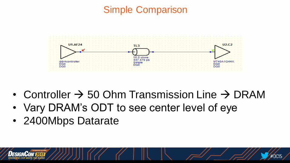
Simple Comparison
• Controller 50 Ohm Transmission Line DRAM
• Vary DRAM’s ODT to see center level of eye
• 2400Mbps Datarate

DDR3 – Sweeping Rx ODT
• No change in Center of eye with ODT

DDR4 – Eye Shifting
• Eye center shifts with ODT change

Vref for a Device
• Need Precision programmable reference voltage
• Center voltage can vary across pins
• Individual Vref per pin may be too expensive
– Silicon and power
• How to determine voltage used for all pins?

Determining Vref – “Avg”
800mV
750mV 730mV 725mV 720mV 710mV 705mV 700mV
• 8 bit device, one Vref resource
• Eye-center of bits different, as below

Determining Vref – Margin Loss
17
Margin Loss for a given bit
Vd = Vref(device) Vx = Vref(pin_x)
𝑀𝑎𝑟𝑔𝑖𝑛 𝐿𝑜𝑠𝑠 = 𝑀𝑝 − 𝑀𝑑 = 𝑉𝑑 − 𝑉𝑥
Note: (The margin “loss” will be negative on the low side waveform in this case
– i.e. a margin gain)
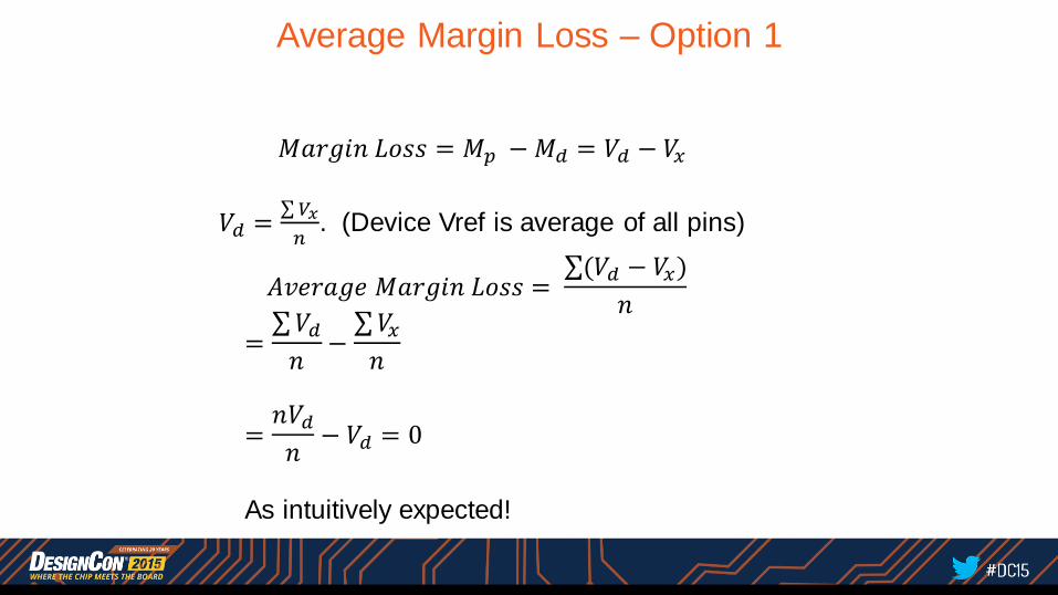
Average Margin Loss – Option 1
= 𝑉𝑑𝑛
− 𝑉𝑥𝑛
=𝑛𝑉𝑑𝑛− 𝑉𝑑 = 0
As intuitively expected!
𝑀𝑎𝑟𝑔𝑖𝑛 𝐿𝑜𝑠𝑠 = 𝑀𝑝 − 𝑀𝑑 = 𝑉𝑑 − 𝑉𝑥
𝑉𝑑 = 𝑉𝑥
𝑛. (Device Vref is average of all pins)
𝐴𝑣𝑒𝑟𝑎𝑔𝑒 𝑀𝑎𝑟𝑔𝑖𝑛 𝐿𝑜𝑠𝑠 =
(𝑉𝑑 − 𝑉𝑥)
𝑛
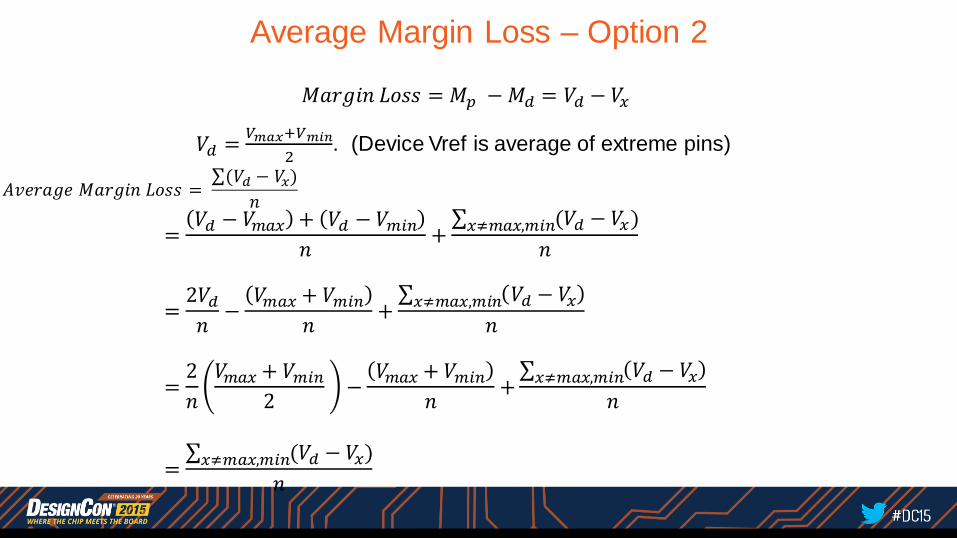
Average Margin Loss – Option 2
=𝑉𝑑 − 𝑉𝑚𝑎𝑥 + 𝑉𝑑 − 𝑉𝑚𝑖𝑛
𝑛+ (𝑉𝑑 − 𝑉𝑥)𝑥≠𝑚𝑎𝑥,𝑚𝑖𝑛
𝑛
=2𝑉𝑑𝑛−𝑉𝑚𝑎𝑥 + 𝑉𝑚𝑖𝑛
𝑛+ 𝑉𝑑 − 𝑉𝑥𝑥≠𝑚𝑎𝑥,𝑚𝑖𝑛
𝑛
=2
𝑛
𝑉𝑚𝑎𝑥 + 𝑉𝑚𝑖𝑛2
−𝑉𝑚𝑎𝑥 + 𝑉𝑚𝑖𝑛
𝑛+ 𝑉𝑑 − 𝑉𝑥𝑥≠𝑚𝑎𝑥,𝑚𝑖𝑛
𝑛
= (𝑉𝑑 − 𝑉𝑥)𝑥≠𝑚𝑎𝑥,𝑚𝑖𝑛
𝑛
𝑀𝑎𝑟𝑔𝑖𝑛 𝐿𝑜𝑠𝑠 = 𝑀𝑝 − 𝑀𝑑 = 𝑉𝑑 − 𝑉𝑥
𝑉𝑑 =𝑉𝑚𝑎𝑥+𝑉𝑚𝑖𝑛
2. (Device Vref is average of extreme pins)
𝐴𝑣𝑒𝑟𝑎𝑔𝑒 𝑀𝑎𝑟𝑔𝑖𝑛 𝐿𝑜𝑠𝑠 =
(𝑉𝑑 − 𝑉𝑥)
𝑛

Average Margin Loss – Comparison
Option 1 always has average margin loss of 0
Option 2 has average margin loss (on one side) of ≥ 0
Shouldn’t we choose Option 1?
No! Consider worst case pins.

Average Margin Loss – Comparison
Option 1: Average of all signals
𝟕𝟑𝟎𝒎𝑽
Option 2: Average of extreme signals
𝟕𝟓𝟎𝒎𝑽
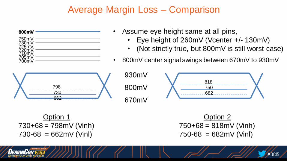
730+68 = 798mV (Vinh)
730-68 = 662mV (Vinl)
750+68 = 818mV (Vinh)
750-68 = 682mV (Vinl)
Average Margin Loss – Comparison
800mV
750mV 730mV 725mV 720mV 710mV 705mV 700mV
Option 1
730+68 = 798mV (Vinh)
730-68 = 662mV (Vinl)
Option 2
750+68 = 818mV (Vinh)
750-68 = 682mV (Vinl)
• Assume eye height same at all pins,
• Eye height of 260mV (Vcenter +/- 130mV)
• (Not strictly true, but 800mV is still worst case)
930mV
670mV
800mV 750 818
682 730 798
662
800mV
• 800mV center signal swings between 670mV to 930mV
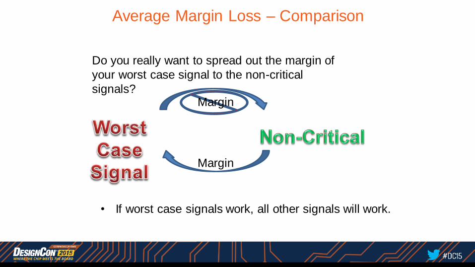
Average Margin Loss – Comparison
Do you really want to spread out the margin of
your worst case signal to the non-critical
signals? Margin
Margin
• If worst case signals work, all other signals will work.
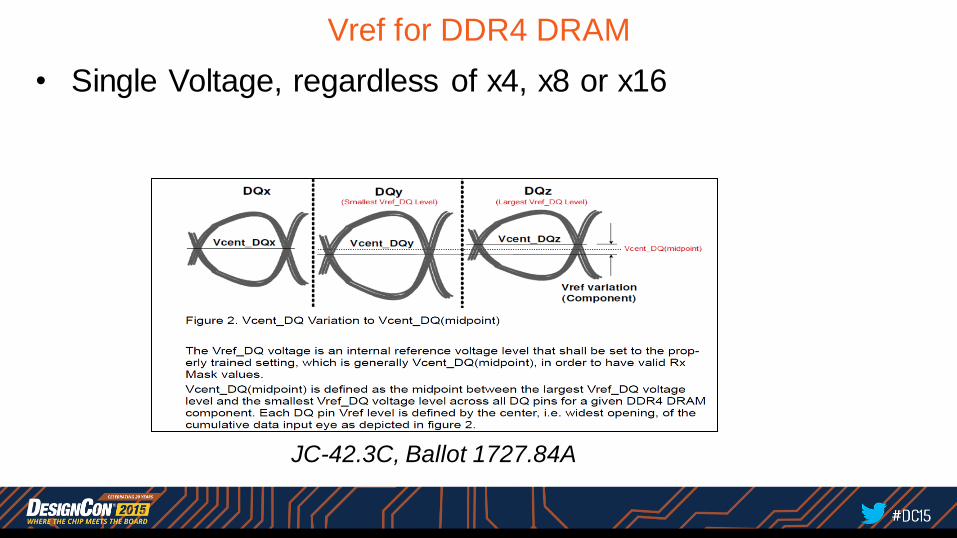
Vref for DDR4 DRAM
• Single Voltage, regardless of x4, x8 or x16
JC-42.3C, Ballot 1727.84A

Vref for DDR4 DRAM
• Range from 45% of Vdd to 92.5% of Vdd
• Step size can be between 0.5%Vddq to 0.8%Vddq – Exact value will be specific to the DRAM and should be in the datasheet

Vref for Controller (Read)
• Single Vref for entire channel
– Inexpensive, easy for controller to implement
– Greater similarity required in DQ signal characteristics

Vref for Controller (Read)
• Single Vref for each DRAM in the rank
– Allows for grouping of signals going to each DRAM

Vref for Controller (Read)
• Single Vref for each Lane in the rank
– Allows for grouping of signals going to each Lane
– Differs from previous setup only for x16 DRAMs

Vref for Controller (Read)
• Single vs. Multi-Rank support
– Cost vs. layoutability
Generating the Eye
• Concept of Eye borrowed from SerDes
• No self-clocking, or clock recovery scheme
• Explicit clock or strobe at play
• In simulation run, cannot just specify frequency
– Must incorporate clock/strobe

Eye - What the Strobe Sees
Double Counted Not Counted

Eye Generation - Folding vs. Strobe
• Data running at 2400MT/s
• Clock P/N slightly offset to simulate poor trace design.

Compare Folding vs. Strobing
DQ Eye Sampled at Strobe
DQ Eye Wrapped at 416.67ps

Enabling DDR4 Simulation
with Power Aware IBIS

I/O Modeling Options
• Simulating SSO is a desired part
of system PDN design
• Choice of I/O model directly
relates to simulation time and
accuracy of SI and PI results
• Common choices include Spice,
IBIS 4.2 and IBIS 5.0.
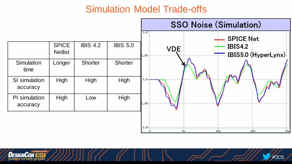
Simulation Model Trade-offs
SPICE
Netlist
IBIS 4.2 IBIS 5.0
Simulation
time
Longer Shorter Shorter
SI simulation
accuracy
High High High
PI simulation
accuracy
High Low High
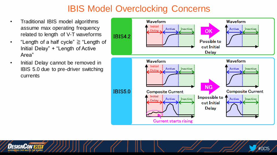
IBIS Model Overclocking Concerns
• Traditional IBIS model algorithms
assume max operating frequency
related to length of V-T waveforms
• “Length of a half cycle” ≧ “Length of
Initial Delay” + “Length of Active
Area”
• Initial Delay cannot be removed in
IBIS 5.0 due to pre-driver switching
currents

Correcting Overclocking in the EDA Software
• Pre-driver and driver currents must
be correctly summed relative to each
switching event
• Must support “Length of a half cycle”
= “Length of Active Area”

Correcting Overclocking in the EDA Software
• Improved simulation
algorithms generate
correct results at every
valid datarate

System Level Simulation

Simulation Schematic
• Includes
Controller,
x32 DQ
bus,
Address/
Command

Simulation Results
• Single net simulation
• Excludes SSO and
Crosstalk
• 2400 Mbps
• Comparison at SDRAM
die pad
• Eye Widths (TdiVW)
within 7ps (1.9%)

Simulation Results
• Simulation includes SSO noise
• 32 DQs and 4 DQ/DQS# pairs switching
• 2400 Mbps
• Comparison of VDE at controller die
• Comparison of DQ at SDRAM die pad
• SSO noise simulated accurately

Simulation Results
• Simulation includes
SSO and Crosstalk
• 1 DQ as Victim net
• 31 DQs and 4
DQ/DQS# pairs as
Aggressor nets
• 2400 Mbps
• Comparison at SDRAM
die pad
• Eye Widths (TdiVW)
within 22ps (7.3%)
• Some mismatch from
un-modeled pre-driver
delay sensitivity
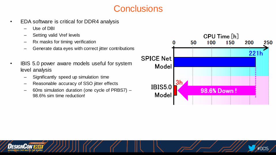
Conclusions
• EDA software is critical for DDR4 analysis
– Use of DBI
– Setting valid Vref levels
– Rx masks for timing verification
– Generate data eyes with correct jitter contributions
• IBIS 5.0 power aware models useful for system
level analysis
– Significantly speed up simulation time
– Reasonable accuracy of SSO jitter effects
– 60ns simulation duration (one cycle of PRBS7) –
98.6% sim time reduction!


