
Department of Electronic Science
University of Delhi SouthCampus
Benito Juarez Road,
New Delhi - 110021

The Department of Electronic Science was established in 1985 and is widely recognised as one of the most prestigious Electronic Science Departments in the country.
The Department is conducting courses leading to M.Tech in Microwave Electronics and M.Sc. in Electronics. The aim of these programmes is to provide the necessary theoretical background and practical experience in order to meet the requirements of the R&D Organizations and Industries. All students joining the M.Sc. course are required to undergo summer training in the Industry or R&D Organisations. In addition, the M.Tech and M.Sc. students work for 6 months on projects in collaboration with Industry and R&D Organisations. The curriculum of these courses is updated regularly to keep it in consonance with the changing industrial environment. The interface with the Industry is further enhanced by an annual seminar under the Visitor’s Programme in which professionals from industry, R&D organizations and academics are invited. Our alumini, now spread over a large number of government and private organisations, facilitate these interactions.
A full range of resources and facilities are available to the students. The department has a well equipped computer laboratory with various circuit simulation and microwave design software for students. In addition, there are well equipped laboratories for experimental work in the following areas: Microwave Measurements, Communication Electronics, Circuit Design, Electrical Machines and Control Systems, Electronic Materials and Semiconductor Devices, Microprocessors and Digital Signal Processing and Optical Electronics. Attempt is made to assess the students’ performance through continuous series of tests and presentations in addition to semester end examinations to ensure highest standards. The Department is actively helping the students in their placement through Campus interviews. Students graduating from the Department have found positions in both government and private organizations working in Space Applications, Telecommunications and Semiconductors.
The students graduating from the programs have the necessary theoretical and practical skills to take on any R&D and Production responsibilities in today’s complex and challenging environment. This is evident from the contributions and achievements of our alumni in organizations like ST Microelectronics, Cadence, HFCL, Aricent, Transwitch, SAMEER, ISRO, DRDO laboratories and many more. The faculty members are actively engaged in research as well as supervision of research leading to the Ph.D. degree in the field of optical electronics, semiconductors, microwaves and microelectronics. The Department has national and international collaborations and several research projects funded by the UGC, CSIR, DST, MIT, AICTE, DRDO, NSF (USA) and JSPS (Japan) and University of Delhi.

FACULTY
S. No.
Name Qualification Designation Specialization
1 Prof. P.K. Bhatnagar Ph.D Professor & Head
Semiconductor and Nano materials, Solid State Devices
2 Prof. E. K. Sharma Ph.D Professor Optical Electronics, Fiber/Integrated Optics and Microwave Photonics
3 Prof. Avinashi Kapoor
Ph.D Professor Photovoltaics, Opto-Electronics, Integrated Optics
4 Prof. Mridula Gupta Ph.D Professor Microelectronics, Communication and Microwaves
5 Dr. Harsupreet Kaur Ph.D Assistant Professor
Microelectronics (Semiconductor Device Modeling and Simulation)
6 Mr. Kamlesh Patel M. Tech. Assistant Professor
Microwave components and characterizations
7 Dr. P. Koteswara Rao
Ph.D, Post-Doc
Assistant Professor
Semiconductor Materials and Devices
8 Mr. Amit Birwal M. Tech. Assistant Professor
Microwave communications

INFRASTRUCTURE FACILITIES
The laboratory training in the department provides students with an exposure to the state of art technologies. This gives them practical skills to meet the growing challenges of industry, R & D and academics. Computer Facility The computer facility of the department is equipped with the latest computers and software packages. A formal course in computational techniques provides all students an understanding of numerical techniques and efficient programming practice in high level programming languages. Students are encouraged to use both FORTRAN 77 and C/C++. Use of mathematical tools like Mathcad and Matlab for solving class assignments is also encouraged. Circuit simulation tools like PSpice and Electronic Workbench as well as powerful simulation and design tools for microwave circuits are also available. Internet connectivity is available in the computer lab and other laboratories of the Department.
Semiconductor Materials and Devices The semiconductor devices and materials laboratory provides experimental setups to study and measure various properties of semiconductor materials. These include Hall measurements, Four -probe method, Vander Pauw Method etc. In addition, characteristics of semiconductor devices like UJT, FET, MOSFET, SCR etc. are also studied. Integrated Circuit Technology has revolutionized electronics . The laboratory provides an exposure to instruments needed in the initial steps for integrated circuits. This includes creation and measurement of vacuum, deposition of thin films on substrates and pattern transfer techniques like photolithography. A C-V plotter is also available to study the characteristics of devices. More recently sophisticated facilities like x-ray diffraction, UV-VIS-NIR spectrophotometer and Kiethley source-meter have been added with support from the DST (FIST) grant. Microprocessors and Digital Signal Processing

The laboratory course provides a system level understanding of the 8086 microprocessor involved in the design of microprocessor based electronic equipment. It involves in depth studies of software architecture, instruction set and assembly level programming with PC interfacing. The students also undertake the programming of the microcontroller 8051 and the interfacing of peripherals. Digital Signal Processing technology and applications have seen a rapid growth over the last decade. An exposure to this technology is provided through TMSC2054 DSP chips in stand alone mode and with a PC interface. It includes programming for arithmetic operations, waveform generation and the more complex filter designs.
Circuit Design and Simulation
The circuit design laboratory focuses on design of both analog and digital circuits. For a better understanding the design exercises are carried out using discrete active and passive components as well as ICs. Circuit design and simulation software packages like Multisim, PSpice VHDL, active HDL and Electronic Workbench are also used for design and simulation before hardware implementation. Kits for FPGA implementation of digital design are also there. This gives the students a first exposure to design tools used in the semiconductor industry. Advanced simulators like 2D ATLAS, 3D ATLAS, MEDICI and ISE TCAD are also available for use in project work by students.
Communication and Control
Communication laboratory provides a package of experiments that give practical understanding and implementation of Analog and Digital Communication Circuits. It includes basic experiments such as AM, FM, PAM, PWM, PCM, DM, and their application in transreceiver systems.
The experiments on system control include SCR controlled DC motor, DC and AC servo motors, error signal generation, angular variation &

analysis, PID control of DC motor with computer interface, Programmable Logic Controller (PLC) and DC Motor Position Control.

Optical Electronics The laboratory begins with simple experiments designed to understand wave phenomena like diffraction, polarization, Fourier Optics with a laser source on an optical bench. Online pattern measurements by a CCD array connected to a PC have also been introduced. This is followed by characterization of optical sources and detectors, optical fibers and demonstration of optical communication. Fiber splicing machine is also there in the Lab. In addition assignments based on the software package “Understanding Fiber Optics on a PC” provide a comprehensive understanding of the optical fibre. A powerful tool for design of integrated optical devices based on the beam propagation method, BPMCAD from OPTIWAVE is also available for design projects. Units for understanding lasing action in Nd-Yag laser and study of non-linear effects have also been introduced.
Microwave Measurements and Electromagnetics
The Microwave laboratory, with benches for experimental work at the X-band, provides the basic training on microwave measurements. These measurements introduce the basic concepts of waveguides and transmission lines, characterization of Gunn and Klystron sources, cavity resonators, directional couplers etc. Measurements on an antenna turn-table provide basic understanding of the antenna radiation pattern and its parameters. Sophisticated equipment such as Network Analyzer with RF source is also available for measurements on Microwave Integrated Circuits. Advanced Microstrip Trainer Kit is also available in the Lab to impart knowledge about microwave circuits using microstrip technology. Department as milling machine for the PCB fabrication facility and on chip Probe Station.
Microwave Integrated Circuits The design and simulation of microwave -integrated circuits forms an important component of the M.Tech. Course. The department has over the time procured some of the best electromagnetic simulators: Ensamble from ANSOFT, IE3D and Empire. Hewlett-- Packard in recognizing the department as a major center of microwave education presented a work-

station and one of the best software tools - EESOF’s advanced design software and Momentum. As part of the curriculum students design and simulate various planar microwave circuits like filters, couplers etc., get them fabricated and finally test them with measurements on the Network Analyzer. Photoluminescence measurement
Photoluminescence (PL) is a versatile tool to qualify thin films, solar cells and Light emitting diodes (LEDs). The photoluminescence signal is strongly influenced by the surface passivation quality and impurity-related transitions, it has been used as a method to measure carrier lifetime.
Atomic Force Microscopy measurement
Atomic force microscopy (AFM) or scanning force microscopy (SFM) is a very high-resolution type of scanning probe microscopy, with demonstrated resolution on the order of fractions of a nano-meter, more than 1000 times better than the optical diffraction limit.
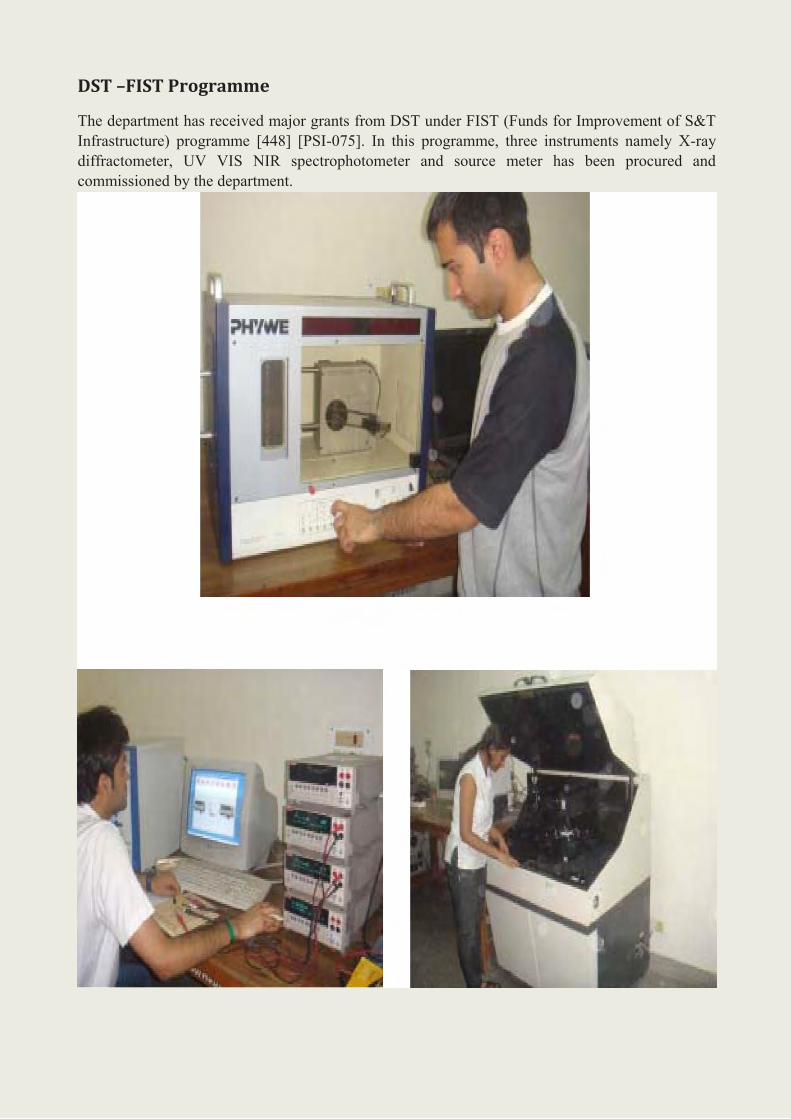
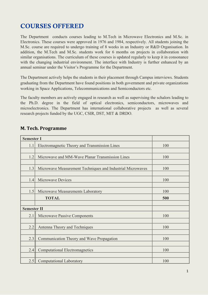
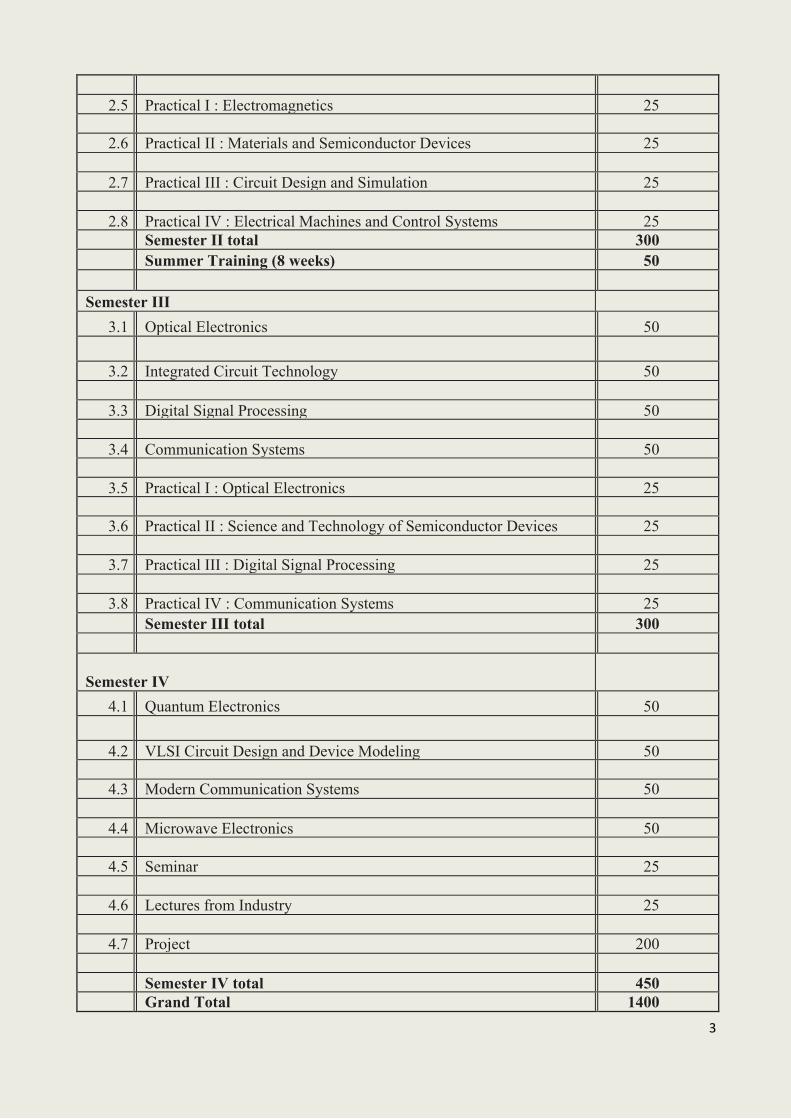
DST –FIST Programme The department has received major grants from DST under FIST (Funds for Improvement of S&T Infrastructure) programme [448] [PSI-075]. In this programme, three instruments namely X-ray diffractometer, UV VIS NIR spectrophotometer and source meter has been procured and commissioned by the department.
1
COURSES OFFERED
The Department conducts courses leading to M.Tech in Microwave Electronics and M.Sc. in Electronics. These courses were approved in 1976 and 1984, respectively. All students joining the M.Sc. course are required to undergo training of 8 weeks in an Industry or R&D Organisation. In addition, the M.Tech and M.Sc. students work for 6 months on projects in collaboration with similar organisations. The curriculum of these courses is updated regularly to keep it in consonance with the changing industrial environment. The interface with Industry is further enhanced by an annual seminar under the Visitor’s Programme for the Department. The Department actively helps the students in their placement through Campus interviews. Students graduating from the Department have found positions in both government and private organizations working in Space Applications, Telecommunications and Semiconductors etc.
The faculty members are actively engaged in research as well as supervising the schalors leading to the Ph.D. degree in the field of optical electronics, semiconductors, microwaves and microelectronics. The Department has international collaborative projects as well as several research projects funded by the UGC, CSIR, DST, MIT & DRDO.
M. Tech. Programme
Semester I
1.1 Electromagnetic Theory and Transmission Lines 100
1.2 Microwave and MM-Wave Planar Transmission Lines 100
1.3 Microwave Measurement Techniques and Industrial Microwaves 100
1.4 Microwave Devices 100
1.5 Microwave Measurements Laboratory 100 TOTAL 500 Semester II
2.1 Microwave Passive Components 100
2.2 Antenna Theory and Techniques 100
2.3 Communication Theory and Wave Propagation 100
2.4 Computational Electromagnetics 100
2.5 Computational Laboratory 100

2
TOTAL 500 Semester III
3.1 Microwave Active Circuits 100
3.2 Communication Systems 100
3.3 Microwave Integrated Circuits 200 (CAD, Fabrication and Measurements) TOTAL 400 Semester IV
4.1 Major Project (six months duration) 400
TOTAL (FOUR SEMESTERS) 1800 M. Sc. Programme
Semester I
1.1 High-level Computer Language and Operating System 50
1.2 Engineering Mathematics 50
1.3 Network Analysis and Synthesis 50
1.4 Advanced Analog and Digital Circuit Design 50
1.5 Practical I : High level Computer Languages and Operating Systems 25
1.6 Practical II : Electronic Circuits 25 1.7 Practical III : Microprocessors 25
1.8 Practical IV : Computational Techniques 25
Semester I total 300 Semester II
2.1 Electromagnetics, Antenna and Propagation 50
2.2 Seminconductor Devices and Materials 50
2.3 Microprocessors 50
2.4 Signal Systems and Control 50
3
2.5 Practical I : Electromagnetics 25
2.6 Practical II : Materials and Semiconductor Devices 25
2.7 Practical III : Circuit Design and Simulation 25
2.8 Practical IV : Electrical Machines and Control Systems 25
Semester II total 300 Summer Training (8 weeks) 50 Semester III
3.1 Optical Electronics 50
3.2 Integrated Circuit Technology 50
3.3 Digital Signal Processing 50
3.4 Communication Systems 50
3.5 Practical I : Optical Electronics 25
3.6 Practical II : Science and Technology of Semiconductor Devices 25
3.7 Practical III : Digital Signal Processing 25
3.8 Practical IV : Communication Systems 25 Semester III total 300 Semester IV
4.1 Quantum Electronics 50
4.2 VLSI Circuit Design and Device Modeling 50
4.3 Modern Communication Systems 50
4.4 Microwave Electronics 50
4.5 Seminar 25
4.6 Lectures from Industry 25
4.7 Project 200
Semester IV total 450 Grand Total 1400
4
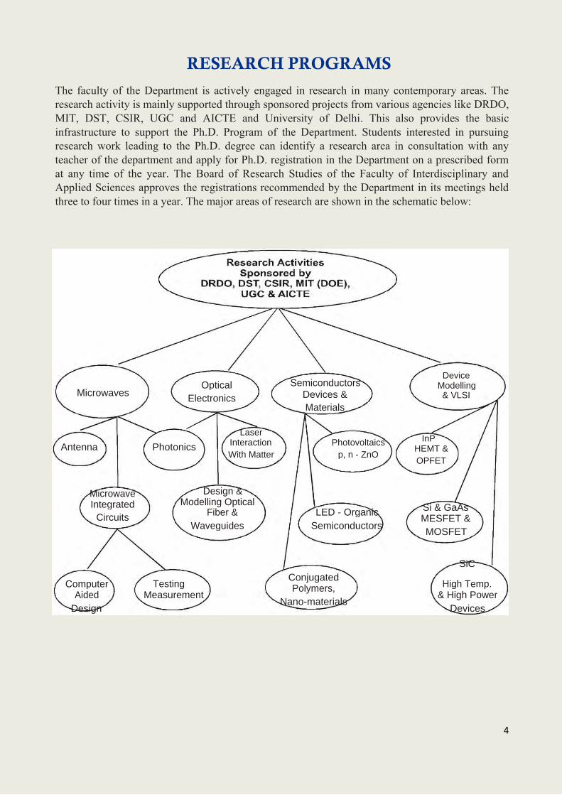
RESEARCH PROGRAMS The faculty of the Department is actively engaged in research in many contemporary areas. The research activity is mainly supported through sponsored projects from various agencies like DRDO, MIT, DST, CSIR, UGC and AICTE and University of Delhi. This also provides the basic infrastructure to support the Ph.D. Program of the Department. Students interested in pursuing research work leading to the Ph.D. degree can identify a research area in consultation with any teacher of the department and apply for Ph.D. registration in the Department on a prescribed form at any time of the year. The Board of Research Studies of the Faculty of Interdisciplinary and Applied Sciences approves the registrations recommended by the Department in its meetings held three to four times in a year. The major areas of research are shown in the schematic below:
Optical Semiconductors
Device
Microwaves Modelling
Devices &
Electronics & VLSI
Materials
Laser InP
Antenna Photonics Interaction Photovoltaics
HEMT &
With Matter p, n - ZnO
OPFET
Microwave Design &
Modelling Optical
Integrated LED - Organic Si & GaAs
Fiber &
Circuits
MESFET &
Waveguides Semiconductors
MOSFET
Computer
Conjugated SiC
Testing
High Temp.
Polymers,
Aided Measurement & High Power
Nano-materials
Design Devices

5
Ph. D. theses completed during (2008 -2013)
S. No. Namer of the student Topic of Ph D Theses
1. Dr. Neha Katyal Investigation of wave mixing in photorefractive materials (Sillenites)
2. Mr. Servin Rathi Modeling, Simulation and Characterization of double gate high electron Mobility Transistor (MEMT) for high power and high frequency Applications with two separate/common modified defferent- metal- insulator geometric control
3. Dr. Priyanka Malik Analytical modeling and simulation of gate dielectric and gate material engineered recessed gate trapezoidal MOSFET in sub-100nm region.
4. Mr. Paramjeet Singh Analysis of Multilayer Lossy Iso/Anisotropic CPW Like Transmission Lines Using Integrated SDA and SLR Methods
5. Dr. Devinder Madhwal Development of Conducting Polymer Based White Light Emitting Diode
6. Mr. Sachin Kumar Sharma
Analytical Modeling and Simulation of Modulation doped field effect transistors
7. Mr. Avneesh Mittal Genetic algoritum based adaptive control systems
8. Mr. Ajay Pratap Singh Theoretical Investigation of optical and transport properties of quantum OOTS in the kondo regime
9. Ms. Neha khanna Dye Sensitised Solar C & U
10. Ms. Pujarini Ghosh Analytical Modeling and Simulation Of Dual Material Gate Stack Architecture Cylindrical/Surrounded Gate MOSFETs.
11. Ms. Shikha Madan Optical and Electrical characterization of 11-VI compound semiconductors quantum dots
12. Ms. Monika Bhattacharya
Modeling, Simulation and Characterization of Noise in InAlAs/InGaAs Tied-geometry Double-gate High Electron Mobility Transistor for Millimeter-wave Applications
13. Ms. Rajni Gautam Analytical Modeling and Simulation of Cylindrical Gate All Around MOSFET- Reliability and Sensor Application
14. Ms. Neetu Singh Dye Sensitised Solar Cell
15. Ms. Renu Guliani Theoretical Modeling and parameter extraction oof dye

6
sensitized solar cell
16. Mr. Y. Premkumar Singh
Theoretical Study of Absorption Enhancement in Silicon Substrate using Plasmonic Nanostructures for Photovoltaic Devices
17. Mr. Anil kumar Study of Surface Plasmon and Lossy Mode Resonances in Optical Waveguides and their application
List of Ph.D research under progress with expected dates of completion:
S.No Name of student Supervisor Date of registration
Expected date of completion
1. Ms Jyoti Bansal Prof. P.K. Bhatnagar July 2009 2014 (Thesis Submitted)
2. Ms. Nainu Priya Chaudhari
Prof. A.K. Verma 2009 2014 (Thesis Submitted)
3. Ms. Rakhi Narang Prof. Mridula Gupta January 2010 2014 (Thesis Submitted)
4. Ms. Vandana Kumari Prof. Mridula Gupta Dr. Manoj Saxena
January 2010 2014 (Thesis Submitted)
5. Khyati Gautam Prof. P.K. Bhatnagar Dr. P. Koteswara Rao
January 2014 January 2018
6. Joginder Singh Prof. P.K. Bhatnagar Dr. P. Koteswara Rao
January 2014 January 2018
7. Varun Singh Nirwal Prof. P.K. Bhatnagar Dr. P. Koteswara Rao
January 2014 January 2018
8. Niharika Kohli Prof. E. K. Sharma November 2011
2015
9. Shivani Sital Prof. E. K. Sharma May 2011 2015
10. Raghvendra Tomar Prof. E. K. Sharma May 2011 2015
11. Anjli Baliyan Prof. E. K. Sharma November 2011
2015
12. Y. Prem Kumar Y Prof. Avinashi Kapoor
2011 2014
13. S. Chaudhary Prof. Avinashi 2011 2014

7
Kapoor
14. Davinder Kaur Prof. Avinashi Kapoor
2012 2016
15. S. Sharma Prof. Avinashi Kapoor
2012 2016
16. N. Gautam Prof. Avinashi Kapoor
2013 2017
17. Sugandha Sharma Prof. Avinashi Kapoor
2014 2018
18. Basant Saini Prof. Avinashi Kapoor
2014 2018
19. Poonam Shokeen Prof. Avinashi Kapoor
2014 2018
20. Yogesh Kumar Prof. Mridula Gupta 2011 2014
21. Jayhind Kumar Verma
Prof. Mridula Gupta April 2013 2017
22. Upasana Kardam Prof. Mridula Gupta April 2013 2017
23. Sachin Tawra Prof. Mridula Gupta July 2013 2017
24. Ajay Singh Prof. Mridula Gupta July 2013 2017
25. Ms. Yashika Gupta Dr. P. Arun 6.1.2014 2018
26. Varun Singh Nirwal Dr. P. Koteswara Rao
6.1.2014 2018
27. Divya Madaan Dr. Vinod Kr. Sharma
6.1.2014 2018

8
Significant Publications of the faculty during 2018-2013
Prof. P. K. Bhatnagar
1. Optical Absorption Spectrum of Single Walled Carbon Nanotubes Dispersed in Sodium Cholate and Sodium Dodecyl Sulfate, Inderpreet Singh, P.K.Bhatnagar, P.C.Mathur, L.M.Bharadwaj, Journal of Material Research, Vol. 23, p632-636, 2008.
2. Development of Low Size Dispersion, High Volume Fraction and Strong Quantum confined CdSxSe1-x Quantum Dots Embedded in Borosilicate Glass Matrix and Study of their Optical Properties, A. Verma, P. K. Bhatnagar, P. C. Mathur, S. Nagpal, P. K. Pandey and J. Kumar, Advanced Materials Research, 31, p 161-163, 2008.
3. A New FRET Based Sensitive DNA Sensor for Medical Diagnostics using PNA Probe and Water Soluble Blue Light Emitting Polymer. Nidhi Mathur, Anamika Aneja, P.K.Bhatnagar and P.C.Mathur. 2008, Accepted in Journal of Sensors. Volume 2008, Article ID 270475, 6 pages (2008) doi:10.1155/2008/270475
4. Triple-FRET Technique for Energy Transfer Between Conjugated Polymer and TAMRA Dye with Possible Applications in Medical Diagnostics. Anamika Aneja, Nidhi Mathur, P.K.Bhatnagar and P.C.Mathur. 2008, Journal of Biological Physics.vol34 p487-493 (2008)
5. Growth Dynamics of II-VI Compound Semiconductor Quantum Dots Embeded in Borosilicate Glass matrix by A.Verma, P.K.Pandey, J.Kumar, S.Nagpal, P.K.Bhatnagar and P.C.Mathur, International Journal of Nanoscience, Vol7, p151-160, June (2008)
6. Two-Photon absorption in Quantum Dots of CdSxSe1-x using open aperture Z- scan and Femto-second laser, Jitender Kumar, A. Verma, P. K. Pandey, P. K. Bhatnagar, P. C. Mathur, M. Bhatnagar, W. Liu and S.H.Tang NANO: brief reports and reviews (world science Net.), Vol 4, 23-29, 2009.
7. Compositional Effect on the Optical Absorption and Photoluminescence of CdSXSe1-XQuantum Dots Embedded in Borosilicate Glasses, Jitender Kumar, A. Verma, P. K. Pandey, P. K. Bhatnagar, P. C. Mathur, M. Bhatnagar, W. Liu and S.H.Tang International Journal of Nanosciences, (Accepted, 1 Feb 2009).
8. Study of optical absorption and Photoluminescence of Quantum Dots of CdS formed in Borosilicate Glass matrix, Jitender Kumar, A. Verma, P. K. Pandey, P. K. Bhatnagar, P. C. Mathur, W. Liu and S.H.Tang Physica Scripta (April ,2009)
9. Optical and electrical characterization of conducting polymer-single walled carbon nanotube composite films. Inderpreet Singh, P.K. Bhatnagar, P.C. Mathur, I. Kaur, L.M. Bharadwaj, R. Pandey. Carbon, Vol. 46, Issue 8, pp 1141-1144, July 2008.

9
10. Study of photoluminescence quenching and DC conductivity measurements in polymer-SWNT composite films for various SWNT concentrations. Inderpreet Singh, P.K. Bhatnagar, P.C. Mathur, I. Kaur, L.M. Bharadwaj, R. Pandey. In special issue of International Journal of Nanotechnology 2009.
11. Development and characterization of an efficient bio-white polymer light-emitting diode with red and green phosphorescent dyes as dopants Devinder Madhwal, S. S. Rait, A. Kumar, A. Verma, K. Tada, M. Onoda, P. K. Bhatnagar and P. C. Mathur Journal of Materials Science Volume 45, Number 12, 3300-3303, DOI: 10.1007/s10853-010-4343-5 (2010)
12.Increased luminance of MEH–PPV and PFO based PLEDs by using salmon DNA as an electron blocking layer”. Devinder Madhwal, S.S. Rait, A. Verma, Amit Kumar, P.K.Bhatnagar, P.C.Mathur, M.Onoda. Journal of Luminescence 130 (2010) 331– 333.
13.The effect of cadmium vacancies on the optical properties of chemically prepared CdS quantum dots by Shikha Madan, Jitender Kumar, Inderpreet Singh, Devinder Madhwal, P K Bhatnagar and P C Mathur Phys. Scr. 82 045702 doi:10.1088/0031- 8949/82/04/045702 (2010).
14. Enhanced luminance of MEH-PPV based PLEDs using single walled carbon nanotube composite as an electron transporting layer by Inderpreet Singh, A. Verma, A.Kumar, S. Rait, I. Kaur, L.M. Bharadwaj, C.S. Bhatia, P.K. Bhatnagar, P.C. Mathur Journal of Luminescence Volume 130, Issue 11, November 2010, Pages 2157–2160
15. Self-trapping mechanism in green phosphorescent dye-doped polymer light-emitting diodes, Devinder Madhwal, S S Rait, A Verma, A Kumar, M Onoda, P. K Bhatnagar and P C Mathur, Physica Scripta Volume 81, 065701 doi:10.1088/0031- 8949/81/06/065701 (2010)
16. A Nano-Biosensor for DNA Sequence Detection Using Absorption Spectra of SWNT-DNA Composite by J. Bansal, I. Singh, N. Mathur, A. Aneja, P.K. Bhatnagar, P.C. Mathur J. Nano- Electron. Phys. 3 (2011) No1, P. 776-782
17. Vinamrita Singh, Swati Arora, P. K. Bhatnagar, Manoj Arora, and R. P. Tandon, Effects of aging on the mobility and lifetime of carriersin organic bulk heterojunction solar cells, Journal of Renewable and Sustainable Energy 3, 063111 (2011) DOI:10.1063/1.3670411
18. Vinamrita Singh,Swati Arora, Pramod Kumar Bhatnagar, Manoj Arora , Ram Pal Tandon, An anomalous behaviour in degraded bulk heterojunction organic solar cells, Accepted for publication in Physica Scripta-2011
19. Swati Arora, Satish Kumar Rajouria, Pankaj Kumar, P K Bhatnagar, Manoj Arora and R P Tandon, Role of donor–acceptor domain formation and interface states in initial degradation of P3HT:PCBM-based solar cells, Phys. Scr. 83 (2011) 035804, (6pp) doi:10.1088/0031-8949/83/03/035804
20. Effect of thermal annealing on the efficiency of poly (3-hexylthiphone):[6,6]-phenyl-C61-butyric acid methyl ester bulk heterojunction solar cells by Inderpreet Singh, Devinder ,Madhwal, Jitender Kumar, Pramod K. Bhatnagar, and Parmatma C. Mathur, Charanjit S. Bhatia Journal of Nanophotonics, vol5,053504 (Apr 11, 2011); doi:10.1117/1.3565485

10
21. Increasing the luminous efficiency of an MEH-PPV based PLED using salmon DNA and single walled carbon nanotube by Devinder Madhwal , Inderpreet Singh, Jitender Kumar, C.S. Bhatia, P.K. Bhatnagar, P.C. Mathur Journal of Luminescence Volume 131, Issue 7, July 2011, Pages 1264–1266
22. Improvement in the luminous efficiency of MEH-PPV based light emitting diodes using zinc oxide nanorods grown by the electrochemical deposition technique on ITO substrates Gupta, Rohini B.; Kumar, Jitender; Madhwal, Devinder; Singh, Inderpreet; Kaur, I.; Bhardwaj, L. M.; Nagpal, S.; Bhatnagar, P. K.; Mathur, P. C., Physica Scripta, Volume 84, Issue 1, pp. 015705 (2011).
23. Color tuning and improved performance of poly[2-methoxy-5-(2′-ethyl-hexyloxy)-1, 4-phenylenevinylene]-based polymer light emitting diode using cadmium selenide/zinc sulphide core shell uncapped quantum dots as dopants by Shikha Madan, Jitender Kumar, Devinder Madhwal, Inderpreet Singh, Pramod Kumar Bhatnagar, and Parmatma Chand Mathur ,J. Nanophoton. 5, 053518 (Aug 09, 2011); doi:10.1117/1.3604001
24.Ultraviolet electroluminescence from zinc oxide nanorods/deoxyribonucleic acid hybrid bio light-emitting diode by Gupta Rohini Bhardwaj; Nagpal Swati; Arora Swati; Bhatnagar Pramod Kumar; Mathur Parmatma Chandra , J. Nanophoton. 5, 059505 (2011)
25. Characterisation of CdSeXS1-X Quantum Dots Using XRD, UV-VIS Absorption and Raman Spectroscopy Measurements by Jitender Kumar, Inderpreet Singh, Shikha Madan ,Devinder Madhwal, P K Bhatnagar and P C Mathur,International Journal of Nanoscience , Accepted for publication, Jan 2012
26. Bulk heterojunction formation with induced concentration gradient from a bilayer structure of P3HT:CdSe/ZnS quantum dots using inter-diffusion process for developing high efficiency solar cell” by Shiv Kumar Dixit, Shikha Madan, Devinder Madhwal, Jitender Kumar, Inderpreet Singh, C.S. Bhatia, P.K.Bhatnagar, P.C.Mathur Organic Electronics Vol. 13, Page 710-15, Jan. 2012.
27. A Environment friendly highly sensitive Ethanol vapor sensor based on Polymethylethacrylate: Functionalized-Multiwall Carbon Nanotubes Composite. Amandeep Kaur, Inderpreet Singh, Jitender Kumar, Devinder Madhwal, P. K. Bhatnagar, P. C. Mathur, C. A. Bernardo and M. C. Paiva Advanced Science and Engineering Medicine 5 1–5, 2013.
28. Bulk heterojunction formation with induced concentration gradient from a bilayer structure of P3HT:CdSe/ZnS quantum dots using inter-diffusion process for developing high efficiency solar cell. Shiv Kumar Dixit , Shikha Madan, Devinder Madhwal , Jitender Kumar, Inderpreet Singh, C.S. Bhatia, P.K. Bhatnagar, P.C. Mathur. Organic Electronics 13 (2012) 710–714.
29. Enhancement of efficiency of a conducting polymer P3HT: CdSe/ZnS quantum dots hybrid solar cell by adding single walled carbon nanotube for transporting photogenerated electrons. S.K. Dixit, S. Madan, A. Kaur, D. Madhwal, I. Singh, P. K. Bhatnagar, P. C. Mathur, C. S. Bhatia, Journal of Renewable and Sustainable Energy, 5 (2013) 033107.
30. J. Bansal, I. Singh, P.K. Bhatnagar, P.C. Mathur “DNA Sequence detection based on Raman Spectroscopy using Single Walled Carbon Nanotube” Published in J of Bioscience and Bioengineering, 2013 Apr,115(4),438-41

11
Prof. Enakshi K. Sharma
1. Analysis Of Cladding Modes In An Asymmetric Dual-Core Fiber, Florence Chan, K. Yasumoto and Enakshi K. Sharma, Microwave and Optical Technology Letters(USA) 51, 507-510 (2009).
2. Er-LiNbo3 Waveguide: Field Approximation for Simplified Gain Calculations in DWDM Application, Geetika Jain, Amita Kapoor and Enakshi K. Sharma, Journal of Optical Society of America B (USA) 26, 633-639 (2009).
3. Analysis of Transmission Characteristics of Long Period Gratings in Tapered Optical Fibers, K.C. Patra, Rashmi Singh, Enakshi K. Sharma and K. Yasumoto, Applied Optics(USA) ,48, G95-G100 (2009).
4. Long Period Grating Refractive Index Sensor: optimal design for single wavelength interrogation, Amita Kapoor and Enakshi K. Sharma, Applied Optics(USA) , 48, G88-G94 (2009).
5. Power exchange in strongly coupled diffused channel waveguide arrays: an analytical approach, KC Patra, S Srivastava and Enakshi Khular Sharma, J. Optics (UK), 12, 1-8, (2010)
6. Saturation characteristics of InGaAsP-InP bulk SOA, Amita Kapoor, Enakshi K Sharma, Wolfgang Freude and Juerg Leuthold, Proc. of SPIE (USA), 7597, (2010).
7. Numerical calculation based study of spectral anomalies and their applications in modified Mach-Zehnder interferometer, Nandan S. Bist, B.K. Yadav, Bhaskar Kanseri, H.C. Kandpal and Enakshi K. Sharma, Optik (Germany), 121, 581-587, (2010).
8. The influence of source and object characteristics on coincidence imaging , Nandan S. Bist, Enakshi K. Sharma and H.C. Kandpal, J. Opt.(UK), 12, 045701 (6pp), (2010).
9. Exprimental observation of lensless ghost imaging by measuring reflected photons, Nandan S. Bist, Enakshi K. Sharma and H.C. Kandpal, Optics and Lasers in Engineering(UK), 48, 671-675, (2010).
10. Effects of thermal light source properties in two-photon subwavelength coincidence interference experiments, Nandan S. Bist, Enakshi K. Sharma and H.C. Kandpal, Optik (Germany), 122, 128-132, (2011).
11. Study of the Amplification Characteristics of a Coaxial EDF with varying coupling conditions, Jyoti Anand, Jagneet Kaur Anand and Enakshi K. Sharma, Optics and Laser Technology (UK), 44, 688-695, (2012).
12. Design and Modeling of Titanium Indiffused LiNbO3 Waveguides for Optimum Coupling to Communication Grade Fiber, Geetika Jain and Enakshi K. Sharma, Journal of Computational and Theoretical Nanoscience (Germany),10, 1326-1334 (2013).
13. Inherent Gain Flattening due to Two Mode Interference in Erbium Doped Coaxial Fibers, Jyoti Anand, Jagneet Kaur Anand and Enakshi Khular Sharma, Optical Fiber Technology, 19, 298-303 (2013).

12
14. Coupled Mode Analysis for Simplified Gain Calculations in Erbium Doped Coaxial Fibers, Jyoti Anand, Jagneet Kaur Anand and Enakshi Khular Sharma,, J. Optical Soc. Of America B, 30, 1496-1502 (2013)
15. Surface Plasmon Resonance based Fiber Optic Sensor for the Detection of Ttriglycerides using Gel Entrapment Technique, Anjli Baliyan, Priya Bhatia, B.D.Gupta, Enakshi K Sharma, Arti Kumari and Rani Gupta, Sensors and Actuators B, 188, 917-922 (2013)

13
Prof. A. K. Verma
1. Nasimuddin, Esselle Karu and Verma A. K. .2007. Wideband Circularly Polarized Stacked Microstrip Antennas. IEEE Antennas and Wireless Propagation Letters, Vol. 6: 21-24
2. Nasimuddin, Esselle Karu and Verma A. K. .2007. Optimizing the Coaxial-Feed Location
to Enhance Circular Polarization Bandwidth of Stacked Microstrip Antennas. Microwave and Optical Tech. Letters, Vol. 49, No. 1, January : pp. 132-135.
3. Nasimuddin, Esselle Karu and Verma A. K. .2008. Wideband High-Gain Circularly Polarized Stacked Microstrip Antennas with an Optimized C-Type Feed and a Short Horn. IEEE Transactions on Antennas and Propagation, Vol 56, No. 2,February: 578-581.
4. Verma A. K., Singh Himanshu. 2009. Circuit Model of Microstrip Step Discontinuity”, International Journal of Microwave and Optical Technology, Vol. 4, No. 2, March: 76-82.
5. Verma A. K., Awasthi Y.K., Singh Himanshu. 2009. Closed-form Model of W/h- Dependent Equivalent Isotropic Relative Permittivity of Microstrip on Multilayer Anisotropic Substrate. International Journal of Microwave and Optical Technology, Vol. 4, No. 2, March: 107-114.
6. Singh Himanshu, Verma A. K., Awasthi Y.K. .2009. Circuit model of multilayer microstrip step discontinuity using SLR formulation”, International Journal of Electromagnetics, Vol. 29, No. 6, July: 483-498.
7. Verma A. K., Awasthi Y.K., Singh Himanshu. 2009. Equivalent Isotropic Relative Permittivity of Microstrip on Multilayer Anisotropic Substrate. International Journal of Electronics, Vol. 96, No .8, August: 865-875.
8. . Awasthi Y.K., Singh Himanshu, Kumar A., Singh P., Verma A. K. . 2009. Accurate CAD-Model Analysis of Multilayer Microstrip Line on Anisotropic Substrate. Journal of Infrared, Millimeter, and Terahertz Waves, 16 October.
9. P. Majumdar and A.K. Verma, “Closed-form Dispersion Models for Propagation Characteristics of Slot-line in Lossy Media with Conductor Thickness,” International Journal of Microwave and Optical Technology, Vol.4,No.2, pp-83-89, March 2009.
10. Majumdar,P , Verma A. K.. 2010. Accurate Closed- form Model for Computation of Conductor Loss of Coplanar Waveguide,” International Journal of RF and Microwave Computer-Aided Engineering, vol. 20, no.1January ,6-14.
11. Majumdar,P , Verma A. K.. 2010. Modified Closed-form Dispersion and Losses Models of Slot-Line with Conductor Thickness,” International Journal of Infrared, Millimeter and Terahertz Waves, vol. 31, no.3, March: 271-287.
12. Y. Ranga, Karu. P. Esselle and A. K Verma, “ Planar-Monopole-Fed, Surface-Mounted Quasi- TEM Horn Antenna for UWB Systems”, IEEE Trans Antenna and Prop. vol 58, no.7 pp.2436-2439, July, 2010.
13. Payal Majumdar and A.K. Verma, “Accurate CAD Model of Stopping Distance to Compute Conductor Loss of CPW,” International Journal of Electronics and

14
Communications, AËU, Vol.64, pp.1157-1166, December 2010. 14. Y. Ranga, Karu. P. Esselle, A. Weily and A. K Verma, “A constant gain printed circular
monopole antenna for UWB applications”, Microwave and Optical Technology Letters, vol. 52, no. 6, June 2010, Pages: 1261-1264.
15. Y. Ranga, Karu. P. Esselle and Andrew R. Weily, “Compact Ultra-Wideband CPW-Fed PrintedSemicircular Slot Antenna,” Microwave and Optical Technology Letters, vol. 52, no. 10, October 2010, Pages: 2367-2372.
16. Payal Majumdar and A.K. Verma, “CAD Models of Losses for Symmetric Elliptical and Circular Cylindrical Coplanar Strip Lines,” Int. Journal of Electronics, Vol. 98, No. 7, pp. 863-882, July 2011.
17. Payal Majumdar and A.K. Verma, “Integrated Closed-form model and Circuit Model of Lossy Slot line,” IET Microwaves, Antennas & Propagation, Vo.5, No.14, 2011, pp.1763-1773.
18. A.K.Verma and Ashwani Kumar ,”Synthesis of Microstrip Lowpass Filter Using Defected Ground Structures” IET Microwaves, Antennas & Propagation, 2011.
19. Payal Majumdar and A.K. Verma, “CAD Models of Losses for Symmetric Elliptical and Circular Cylindrical Coplanar Strip Lines,” Int. Journal of Electronics, Vol. 98, No. 7, pp. 863-882, July 2011.
20. Payal Majumdar and A.K. Verma, “Integrated Closed-form model and Circuit Model of Lossy Slot line,” IET Microwaves, Antennas & Propagation, vol. 5 ,No. 14 November 18 2011, pp. 1763-1772 .
21. A.K.Verma, Ashwani Kumar “Design of Low Pass Filters using Some Defected Ground Structures”, International Journal of Electronics and Communications Elsevier, Volume 65, Issue 10, Pages 864-872, October 2011.
22. A.K.Verma, Ashwani Kumar, “Synthesis of Microstrip Low pass Filter Using Defected Ground Structures”, IET Microwaves, Antennas & Propagation, Volume: 5 Issue:12, page(s): 1431 - 1439. September 16 2011.
23. Anand K. Verma, ,Adel Abdel-Rahman, Ashwani Kumar , Nainu P. Chaudhari, Atallah Balalem and Abbas Omar, "New Compact Dual-Band Bandstop Filter" International Journal of Electronics,Taylor & Francis.
24. A. K. Verma, Paramjeet Singh, “Loss Computation of Multilayer Coplanar Waveguide using Single Layer Reduction Method”, International Journal of Electromagnetics and Applications (IJEA), Vol. 2, No. 6, November 2012, pp. 174-181.
25. A.. K. Verma, Paramjeet Singh, Ritu Bansal, “Computation of Static and Frequency Dependent Line Parameters of Multilayer CPW using Static SDA and Single Layer Reduction Method”, International Journal of RF and Microwave Computer-Aided Engineering, (Accepted).
26. A. K. Verma, Paramjeet Singh, Ritu Bansal, “Modeling for Dispersion and Losses of

15
Multilayer Asymmetric CPW on Iso/Anisotropic Substrate”, Progress In Electromagnetics Research B (PIER-B), Vol. 48, February 2013, pp. 395-419.
27. Anand K. Verma, Nainu P. Chaudhari, and Ashwani Kumar, „High Performance Microstrip Transverse Resonance Lowpass Filter”, Microwave Optical Tech. Letters, Vol. 55, May 2013.
28. Anand K. Verma, Nainu P. Chaudhari, and Ashwani Kumar, “ Improved performance step impedance lowpass filter”, Int. J. Electron. Commun. (AEÜ) 67 (2013) 754– 760

16
Prof. A. K. Kapoor
1. Single layer Homogeneous model for surface roughness by polarized light scattering, Udaibir Singh and Avinashi Kapoor, Optics and Laser Technology, Volume 40, Issue 2, Pages 315-324, March 2008 2. Effect of S and P Polarization on single layer Homogeneous model, Udaibir Singh and Avinashi Kapoor, Proc. of SPIE, 6720, Art. No. 67201R, 2008 3. Consistency and Variations in optical characteristics of four-layer polymeric waveguides, Rajesh Kumar, Amit Pratap Singh, Avinashi Kapoor, K.N. Tripathi, Optik, 119(12), 553-558, 2008. 4. Effects of deposition temperature on the structural and morphological properties of thin ZnO films fabricated by pulsed laser deposition”, Rakhi Khandelwal, Amit P Singh, Avinashi Kapoor, Sorin Grigorescu, Paola Miglietta, Nadya E Stankova and Alessio Perrone, Optics and Laser Technology, Volume 40, Issue 2, Pages 247-251, 2008. 5. Effects of deposition temperature on the structural and morphological properties of SnO2 films fabricated by pulsed laser deposition”, Rakhi Khandelwal, Amit P Singh, Avinashi Kapoor, Sorin Grigorescu, Paola Miglietta, Nadya E Stankova and Alessio Perrone, Optics and Laser Technology, Volume 41, Issue 1, Pages 89-93, 2009 6. Quantum Dot Solar Cell: An Overview Partha Goswami, Garima Puneyani, Naorem Santakrus Singh and Avinashi Kapoor, Published in Research Signpost review book "Applied Physics in the 21st Century", 2008, 159-183. 7. Extraction of parameters of a real solar cell-A review article”, Amit Jain and Avinashi Kapoor, Published in Research Signpost review book "Applied Physics in the 21st Century", 2008, 131-158. 8. Inducement of spin-pairing and correlated semi-metallic state in Mott-Hubbard quantum dot array, Partha Goswami and Avinashi Kapoor, Physica E, Volume 41, Pages 379-386, 2009.
9. Tuning of PID Parameters Using Artificial Neural Network, Nisha, Avneesh Mittal , O.P.Sharma , Nitu Dhyani, Vijay Sharma, Avinashi Kapoor and T.K. Saxena, 2009, IEEE-Xplore, pp 309-312. 10. Determination of the solar cell junction ideality factor using special tans function theory (STFT), N. Santakrus Singh, Amit Jain, Avinashi Kapoor, Solar Energy Materials & Solar Cells, Volume 3(2009), 1423-1426. 11. Influence of pump beam Polarization on signal beam in photorefractive crystal in TWM : transmission geometry”, Neha Katyal, Natasha, Amitava Roy, Avinashi Kapoor, Optik, 2010.

17
12. Investigation of transmittance property of Palladium thin film fabricated by pulsed laser deposition with polarization using single layer model, Udaibir Singh, Nisha Jha, Tikendra Prakash Singh, Avinashi Kapoor and Alessio Perrone, Optics and Laser Technology, 42 (2010)1128-1133
13. Designing & Development of Static System for controlling temperature using NNPID, Nisha Jha, Udaibir Singh, Avinashi Kapoor, Sajosps, 2010 , vol. 11, No. 1, 127-131. 14. High extinction ratio metal–insulator–semiconductor waveguide surface plasmon polariton polarizer V.K. Sharma, Anil Kumar, Avinashi Kapoor, Optics Communications Vol.284 pp.1815-1821, 2011
15. Modeling of Dye Sensitized Solar Cells, Neetu Singh, R.M. Mehra, Avinashi Kapoor, Invertis Journal of Renewable Energy Vol. 1, No. 1, 2011, pp. 51-61 16. Optimal Design of Neural Fuzzy Inference Network for Temperature Control, Nisha Jha, Udaibir Singh, T.K. Saxena and Avinashi Kapoor, Journal of Applied Sciences, 2011. 17. Online Adaptive Control for Non Linear Processes under influence of External Disturbance, Nisha Jha, Udaibir Singh, T.K. Saxena and Avinashi Kapoor, International Journal of Artificial Intelligence and Expert System (IJAE), Vol. 2, Issue 2, pp. 36-46., 2011 18. Synthesis and characterization of ZnO nanoparticles, Neetu Singh, R.M. Mehra, Avinashi Kapoor, J. Nano- Electron. Phys. (JNEP), accepted 2011, Vol. 3, (2011) No1, P.132-139. 19. Analysis of surface and guided wave plasmon polariton modes in insulator–metal– insulator planar plasmonic waveguides, V.K. Sharma, Anil Kumar, A. Kapoor, Optics Communications, Vol.285,pp.1123–1127,2012 20. Integrated optic TE/TM pass polarizers using resonant coupling between ITO thin film lossy modes and dielectric waveguide modes, Anil Kumar, V.K. Sharma, D. Kumar, A. Kapoor, Accepted for publication in Optics Communications, 2012 21. Disorder induced semiconductor to metal transition and modifications of grain boundaries in nanocrystalline zinc oxide thin film, Fouran Singh, Babloo Chaudhary, Vinod Kumar, R. G. Singh, Sanjeev Kumar, J. Appl. Phys., 2012, 112, 073101.
22. Genetic algorithm based incremental PID temperature controller for long dead time nonlinear bath, Avneesh Mittal, Avinashi Kapoor, T. K. Saxena, IJESR June 2012, Volume-2/Issue-6/Article No-6/449-467. 23. Genetic algorithm based tuning of fixed bias PID controller for a nonlinear constant

18
temperature water bath under load disturbances, Avneesh Mittal, Avinashi Kapoor, T. K. Saxena, JASE 6-2, 2012, 96-109.
24. Enhancement in light coupling into silicon solar cells using low cost and earth abundant aluminium nanoparticles, Y. Prem Kumar Singh, Amit Jain, A. Kapoor, International Journal of Engineering and Applied Sciences, Vol. 1, 2012, 86-90. 25. An exact analytical method for calculating the parameters of a real solar cell using special trans function theory (STFT), IJRER, Jan 2013.
26. Enhancement in Optical Absorption of Plasmonic Solar Cells, Y. Premkumar Singh, Anil Kumar, Amit Jain and A. Kapoor, The Open Renewable Energy Journal, Vol. 6, 2013, 1-6. 27. Role of film thickness on the properties of ZnO thin films grown by sol-gel method, Vinod Kumar, Neetu Singh, R. M. Mehra, Avinashi Kapoor and L. P. Purohit, H.C. Swart, Thin Solid Films (2013), Elsevier 28. Genetic Algorithm based Neuro Fuzzy Tuning of PID Controller for a Nonlinear Temperature Water Bath with Feedforward Control, Avneesh Mittal, Priyanka Jain, Avinashi Kapoor, T. K. Saxena, IEEE Xplore: 978-1-4799-1441-8/13/$31.00 ©2013 IEEE, pp:34-38. 29. High efficiency hybrid solid state blended dyes sensitized solar cell based on zinc oxide nanostructures, R. G. Singh, Naina Gautam, Subodh K. Gautam, Vinod Kumar and A. Kapoor, Journal of Renewable and Sustainable Energy, Vol. 5, 2013, 033134- 1-8 30.Adaptive Tuning of PID Controller for a Nonlinear Constant Temperature Water Bath under Set Point Disturbances using GANFC Avneesh Mittal, Avinashi Kapoor, T. K. Saxena J. Automation & Systems Engineering (Communicated)

19
Prof. Mridula Gupta
1. Temperature dependent analytical model of sub-micron GaN MESFETs for microwave frequency applications, Sneha Kabra, Harsupreet Kaur, Subhasis Haldar, Mridula Gupta and R.S. Gupta, Solid State Electronics, Vol. 52, Pp. 25-30, 2008.
2. Multi-material gate poly-crystalline thin film transistors: Modeling and simulation for an improved gate transport efficiency, version 3 Amit Sehgal, Tina Mangla, Mridula Gupta, R. S. Gupta, Thin Solid Films, Vol. No. 516, Pp. 2162-2170, 2008.
3. Analytical Performance Evaluation of AlGaN/GaN Metal Insulator Semiconductor Heterostructure Field Effect Transistor (MISHFET) and its Comparison with Conventional HFETs for High Power Microwave Applications, Ruchika Aggarwal, Anju Agrawal, Mridula Gupta and R.S. Gupta, Microwave and Optical Technology Letters, Vol. 50, No. 2, P.331 – 338, (February) 2008.
4. Laterally amalgamated Dual Material Gate Concave (L-DUMGAC) MOSFET for ULSI, Rishu Chaujar, Ravneet Kaur, Manoj Saxena, Mridula Gupta and R.S. Gupta, Microelectronic Engineering, Vol. 85, Pp. 566 – 576, March 2008.
5. Dual Material Double Layer Gate Stack SON MOSFET: A Novel Architecture for enhanced analog performance – Part I Impact of Gate Metal Workfunction Engineering, Poonam Kasturi, Manoj Saxena, Mridula Gupta and R.S. Gupta, IEEE Transactions on Electron Devices, Vol. 55, No. 1, Pp. 372-381, 2002008
6. Dual Material Double Layer Gate Stack SON MOSFET: A Novel Architecture
for enhanced analog performance – Part II Impact of Gate Dielectric Material Engineering, Poonam Kasturi, Manoj Saxena, Mridula Gupta and R.S. Gupta, IEEE Transactions on Electron Devices, Vol. 55, No. 1, Pp. 382-387, 2008.
7. Two-dimensional analytical sub-threshold model of multi-layered gate dielectric recessed channel (MLaG-RC) nanoscale MOSFET, Rishu Chaujar, Ravneet Kaur, Manoj Saxena, Mridula Gupta and R.S. Gupta, Semiconductor Science and Technology, Vol. 23, No. 4, (10pp), April 2008.
8. Analytical modeling and simulation of subthreshold behavior in nanoscale dual material gate AlGaN/GaN HEMT, Sona P. Kumar, Anju Agrawal, Rishu Chaujar, Mridula Gupta and R.S. Gupta, Superlattices and Microstructures, Vol. 44, No. Pp. 37-53, July 2008.
9. Graded Channel Architecture: the Solution for Misaligned DG FD SOI n-MOSFETs, Rupendra Kumar Sharma, Ritesh Gupta, Mridula Gupta and R. S. Gupta, Semiconductor Science and Technology, Vol. 23, No. 7, Pp., 075041, 2008.
10. Intermodulation Distortion and Linearity Performance Assessment of 50-nm gate length LDUMGAC MOSFET for RFIC Design, Rishu Chaujar, Ravneet Kaur, Manoj Saxena, Mridula Gupta and R.S. Gupta, Superlattices and Microstructures, Vol. 44, Pp.143-152, 2008.

20
11. TCAD Assessment of Gate Electrode Workfunction Engineered Recessed Channel (GEWE-RC) MOSFET and its Multi-Layered Gate Architecture: Part-I: Hot Carrier Reliability Evaluation, Rishu Chaujar, Ravneet Kaur, Manoj Saxena, Mridula Gupta and R.S. Gupta, IEEE Transactions on Electron Devices, Vol. 55, No. 10, Pp. 2602-2613, 2008.
12. On-State and RF Performance Investigation of Sub-50nm L-DUMGAC MOSFET Design for High-Speed Logic and Switching Applications, Rishu Chaujar, Ravneet Kaur, Manoj Saxena, Mridula Gupta and R.S. Gupta, Semiconductor Science and Technology, Vol. 23, 095009 (8pp), 2008.
13. Gate Dielectric Engineering of Quarter Sub Micron AlGaN/GaN MISHFET: A New Device Architecture for Improved Transconductance and High Cut-off Frequency, Ruchika Aggarwal, Anju Agrawal, Mridula Gupta and R.S. Gupta, Solid State Electronics, Vol. 52, Pp. 1610-1614, 2008.
14. Modeling and Analysis of Fully Strained and Partially Relaxed Lattice Mismatched AlGaN/GaN HEMT for High Temperature Applications, Parvesh Gangwani, Ravneet Kaur, Sujata Pandey, Subhasis Haldar, Mridula Gupta and R.S. Gupta, Superlattices and Microstructures, Vol. 44, No. 6, Pp. 781-793, Dec. 2008.
15. Two-dimensional threshold voltage model and design considerations for gate electrode workfunction engineered recessed channel (GEWE-RC) nanoscale MOSFET: part 1, Rishu Chaujar, Ravneet Kaur, Manoj Saxena, Mridula Gupta and R.S. Gupta, Semiconductor Science and Technology, Vol. 23, 045006 (10pp), 2008.
16. Two-Dimensional Analytical Subthreshold Model of Graded Channel DG FD SOI n-MOSFET with Gate Misalignment Effect, Rupendra Kumar Sharma, Mridula Gupta and R.S. Gupta, Superlattices and Microstructures, Vol. 45, Pp. 91-104, 2009.
17. T-gate geometric (solution for submicrometer gate length) HEMT: Physical analysis, modeling and implementation as parasitic elements and its usage as dual gate for variable gain amplifiers, Ritesh Gupta, Servin Rathi, Ravneet Kaur, Mridula Gupta, R.S. Gupta, Superlattices and Microstructures, Vol. 45, No. 3, Pp. 105-116, 2009.
18. Investigation of Multi-Layered-Gate Electode Workfunction Engineered Recessed Channel (MLGEWE-RC) Sub-50nm MOSFET: A Novel Design, Rishu Chaujar, Ravneet Kaur, Manoj Saxena, Mridula Gupta and R.S. Gupta, International Journal of Numerical Modelling: Electronic Networks, Devices and Fields, Vol. 22, No. 3, Pp. 259-278, May/June 2009.
19. Dynamic Performance of Graded Channel DG FD SOI n-MOSFETs for Minimizing the Gate Misalignment Effect, Rupendra Kumar Sharma, Mridula Gupta and R.S. Gupta, Microelectronics Reliability, Vol. 49, No. 6, pp. 592-599, June 2009.
20. Dual-material double-gate SOI n-MOSFET: Gate misalignment analysis, Rupendra Kumar Sharma, Ritesh Gupta, Mridula Gupta and R.S. Gupta, IEEE Transactions on Electron Devices, Vol. 56, No. 6, 1284–1291, 2009.

21
21. TCAD assessment of gate electrode workfunction engineered recessed channel (GEWE-RC) MOSFET and its multi-layered gate architecture: Part II: Analog and large signal performance evaluation, Rishu Chaujar, Ravneet Kaur, Manoj Saxena, Mridula Gupta and R.S. Gupta, Superlattices and Microstructeres, Vol. 46, No. 4, Pp. 645-655, October 2009.
22. Modeling of hetero-interface potential and threshold voltage for tied and separate nanoscale InAlAs-InGaAs symmetric double-gate HEMT, Servin Rathi, Jyotika Jogi, Mridula Gupta, R.S. Gupta, Microelectronics Reliability, Vol. 49, pp. 1508-1514, 2009.
23. Design considerations and impact of technological parametric variations on RF/microwave performance of GEWE-RC MOSFET, Rishu Chaujar, Ravneet Kaur, Manoj Saxena, Mridula Gupta and R.S. Gupta, Microwave and Optical Technology Letters, Vol. 53, No. 3, P.652-657, 2010.
24. Gate Material Engineered-Trapezoidal Recessed Channel MOSFET (GME-TRC) for High Performance Analog and RF Applications, Priyanka Malik, Sona P. Kumar, Rishu Chaujar, Mridula Gupta & R.S. Gupta, Microwave and Optical Technology Letters, Vol. 53, No. 3, P.694-698, 2010.
25. Metal Insulator Gate Geometric HEMT: Novel Attributes and Design Consideration for High Speed Analog Applications, Ritesh Gupta, Ravneet Kaur, Sandeep Kr Aggarwal, Mridula Gupta, and R. S. Gupta, Journal of Semiconductor Technology and Science, Vol.10, No.1, 66-77, (March), 2010.
26. Analytical modeling of Channel noise for Gate Material Engineered Surrounded/Cylindrical Gate (SGT/CGT) MOSFET, Pujarini Ghosh, Rishu Chaujar, Subhasis Haldar, R.S Gupta and Mridula Gupta, World Academy of Science, Engineering and Technology No.40, 620-623, 2010.
27. Two-dimensional Analytical Drain Current Model for Multilayered-Gate Material Engineered Trapezoidal Recessed Channel (MLGME-TRC) MOSFET: a Novel Design, Priyanka Malik, Rishu Chaujar, Mridula Gupta, R.S. Gupta, World Academy of Science, Engineering and Technology vol. 40, pp. 472-476, 2010.
28. Microwave performance enhancement in Double and Single Gate HEMT with channel thickness variation. Ritesh Gupta, Servin Rathi, Mridula Gupta and R S Gupta, Superlattice and Microstructures, Vol. 47, No. 6, P. 779-794, (June) 2010.
29. An analytical charge-based drain current model for nanoscale In0.52Al0.48As-In0.53Ga0.47 As separated double-gate HEMT, Servin Rathi, Jyotika Jogi, R.S. Gupta and Mridula Gupta, Semiconductor Science and Technology, Vol. 25, No.11, P. 115003-115009, (Oct) 2010.
30. Physics Based Threshold voltage analysis of Gate Material Engineered Trapezoidal Recessed Channel (GME TRC) Nanoscale MOSFET and its Multilayered gate architecture, Priyanka Malik, Rishu Chaujar, Mridula Gupta and R.S Gupta. International Journal of Microwave and Optical Technology, Vol.5, No.6, P.361-368, (Nov) 2010.

22
31. Device linearity and intermodulation distortion comparison of Dual Material Gate and conventional AlGaN/GaN High Electron Mobility Transistor, Sona P Kumar, Anju Agrawal, Rishu Chaujar, Mridula Gupta and R.S. Gupta. Microelectronics Reliability. Vol. 51, No.3, P. 587-596, (March) 2011.
32. Improved Linearity Performance of AlGaN/GaN MISHFET over Conventional HFETs: An Optimization Study for Wireless Infrastructure Applications, Ruchika Aggarwal, Anju Agrawal, R.S Gupta. and Mridula Gupta. Superlattices and Microstructures. Vol.50, No. 1, P.1-13, (July) 2011.
33. Scattering parameter based Modeling and Simulation of symmetric tied-gate InAlAs/InGaAs DG-HEMT for millimeter-wave applications, Monika Bhattacharya, Jyotika Jogi, R.S Gupta and Mridula Gupta. Solid State Electronics, Vol.63, No.1, P.149-153, (September) 2011.
34. TCAD Assessment of Device Design Technologies for Enhanced Performance of Nanoscale DG MOSFET, Rupendra Sharma, Mridula Gupta and R.S Gupta, IEEE Trans. Electron Devices. Vol. 58, No. 9, P. 2936-2943, (September), 2011.
35. Linearity-Distortion analysis of GME-TRC MOSFET for High Perfromance and Wireless Applications, Priyanka Malik, R.S.Gupta, Rishu Chaujar and Mridula Gupta, Journal of Semiconductor Technology and Science, P. 152-174, (July) 2011.
36. AC Analysis of nanoscale GME-TRC MOSFET for Microwave and RF Applications, Priyanka Malik, R.S.Gupta, Rishu Chaujar and Mridula Gupta. Microelectronic Reliability, Vol. 52, no. 1, pp. 151-158, (January) 2012.
37. Impact of Interface Fixed Charges on the Performance of the Channel Material Engineered Cylindrical Nanowire MOSFET, Rajni Gautam, Manoj Saxena, R.S. Gupta , and Mridula Gupta, AIRCC journal (International journal of VLSI design & Communication Systems VLSICS ), Vol. 1, No. 3, P. 225-241, (September), 2011.
38. Linearity and Analog Performance Analysis of Double Gate Tunnel Fet: Effect of Temperature and Gate Stack, Rakhi Narang, Manoj Saxena, R. S. Gupta and Mridula Gupta, International journal of VLSI design & Communication Systems ( VLSICS).,Vol. 2, No. 3, P.185-200, (September), 2011.
39. An Analytical Drain Current Model for Dual Material Engineered Cylindrical/Surrounded Gate MOSFET, Pujarini Ghosh, Subhasis Haldar, R.S. Gupta, and Mridula Gupta, Microelectronics Journal Vol. 43, No. 1, pp.17-24, 2012.
40. Dielectric Modulated Tunnel Field Effect Transistor – A Bio molecule Sensor, Rakhi Narang, Manoj Saxena, R.S. Gupta, and Mridula Gupta, IEEE Electron Device Letters, vol. 33, no. 2, pp. 266-268, Feb 2012.
41. Two Dimensional Analytical Subthreshold Model of Nanoscale Cylindrical Surrounding Gate MOSFET Including Impact of Localised Charges, Rajni Gautam, Manoj Saxena, R.S.Gupta and Mridula Gupta, Journal of computational and theoretical nanoscience, Vol.9, No.4, p.602-610. (April) 2012.
42. Simulation Study of Insulated Shallow Extension Silicon On Nothing (ISESON)

23
MOSFET for High Temperature Applications, Vandana Kumari, Manoj Saxena, R.S. Gupta, and Mridula Gupta, Microelectronics Reliability Vol.52, No.8, pp.1610:1612 (August), 2012.
43. Gate-Geometric Recessed Nano-scale In0.52Al0.48As-In0.53Ga0.47As Double–Gate HEMT for High Breakdown, Servin Rathi, Mridula Gupta and R. S. Gupta, IEEE Transaction on Device and Material Reliability Vol. 12, No. 1, pp.139-145, 2012.
44. Effect of Localised Charges on Nanoscale Cylindrical Surrounding Gate MOSFET: Analog Performance and Linearity Analysis, Rajni Gautam, Manoj Saxena, R.S.Gupta and Mridula Gupta, Microelectronics Reliability, vol. 52, no.6, pp. 989-994, June 2012.
45. Immunity against Temperature Variability and Bias point Invariability in Double Gate Tunnel Field Effect Transistor, Rakhi Narang, Manoj Saxena, R.S. Gupta, and Mridula Gupta, Microelectronics Reliability, Vol.52, No.8, pp.1617-1620. (August) 2012.
46. Temperature Dependent Drain Current Model for Gate stack Insulated Shallow Extension Silicon on Nothing (ISESON)MOSFET for wide operating temperature range, Vandana Kumari, Manoj Saxena, R.S. Gupta, and Mridula Gupta, Microelectronics Reliability. Vol. 52, no. 6, pp. 974–983, June 2012.
47. Analog and Digital Performance Assessment of Empty Space in Double Gate (ESDG) MOSFET: A Novel Device Architecture, Vandana Kumari, Manoj Saxena, R.S. Gupta, and Mridula Gupta, Journal of computational and theoretical nanoscience (JCTN), Vol. 10, no. 2, pp.389-398, 2013.
48. An Accurate Charge-Control- Based Approach for Noise Performance Assessment of a Symmetric Tied-Gate INAlAs/INGaAs DG HEMT, Monika Bhattacharya, Jyotika Jogi, R.S Gupta and Mridula Gupta, IEEE Transactions on Electron Devices, Vol. 59 , no. 6, pp. 1644 – 1652, June 2012
49. Analytical Model for Double-Gate Tunneling Field-Effect Transistor (DG-TFET) using carrier concentration approach, Rakhi Narang, Manoj Saxena, R.S. Gupta, and Mridula Gupta, Journal of Computational and Theoretical Nanoscience (JCTN). Vol. 10, no. 5, pp.1-7, 2013.
50. Two dimensional analytical drain current model for Double Gate MOSFET incorporating Dielectric Pocket (DP-DG), Vandana Kumari, Manoj Saxena, R.S. Gupta, and Mridula Gupta, IEEE Transactions On Electron Devices, vol 59, no. 10, pp. 2567 - 2574, 2012.
51. A Dielectric Modulated Tunnel FET based Biosensor for Label Free Detection: Analytical Modeling Study and Sensitivity Analysis, Rakhi Narang, K. V. S. Reddy, Manoj Saxena, R.S. Gupta, and Mridula Gupta, IEEE Transactions on Electron Devices, vol. 59, no. 10, pp. 2809-2817, Oct 2012.
52. An Accurate Small Signal Modeling of Cylindrical/Surrounded Gate MOSFET for High Frequency Applications, Pujarini Ghosh, Subhasis Haldar, R.S.Gupta and Mridula Gupta. Journal of Semiconductor Technology and Science, Vol. 12, no. 4, pp. 377-387, 2012.

24
53. Analytical Modeling and Simulation for Dual Metal Gate Stack Architecture (DMGSA) Cylindrical/Surrounded Gate MOSFET, Pujarini Ghosh, Subhasis Haldar, R.S.Gupta and Mridula Gupta. Journal of Semiconductor Technology and Science, Vol. 12, no. 4, pp. 458-466, 2012.
54. An Investigation of Linearity Performance and Intermodulation Distortion of GME CGT MOSFET for RFIC Design, Pujarini Ghosh, Subhasis Haldar, R.S.Gupta and Mridula Gupta, IEEE Transactions on Electron Devices, Vol. 59, no.12, pp. 3263-3268, 2012.
55. Numerical Model of Gate All Around MOSFET With Vacuum Gate Dielectric For Biomolecule Detection, Rajni Gautam, Manoj Saxena, R.S.Gupta, and Mridula Gupta, IEEE Electron Device Letters, vol.33, no.12, pp. 1756-1758, 2012.
56. “Numerical analysis of localised charges impact on Static and Dynamic Performance of Nanoscale Cylindrical Surrounding Gate MOSFET Based CMOS Inverter”, Rajni Gautam, Manoj Saxena, R. S. Gupta, and Mridula Gupta, Microelectronics Reliability, Vol. 53, Issue 2, Pages 236–244, 2013.
57. Assessment of Ambipolar Behavior of a Tunnel FET and Influence of Structural Modifications, Rakhi Narang, Manoj Saxena, R.S. Gupta, and Mridula Gupta, Journal of Semiconductor Technology and Science, Vol. 12, no. 4, pp. 482-491, 2012.
58. Investigation of Empty Space in Nanoscale Double Gate (ESDG) MOSFET for High Speed Digital Circuit Applications, Vandana Kumari, Manoj Saxena, R.S. Gupta, and Mridula Gupta, Journal of Semiconductor Technology and Science, Vol. 13, no. 2, pp.127-138, 2013.
59. Device and Circuit Level Performance Comparison of Tunnel FET Architectures and Impact of Heterogeneous Gate Dielectric, R. Narang, M. Saxena, R. S. Gupta and M. Gupta, Journal of Semiconductor Technology And Science, Vol. 13, no. 3, pp. 224-236, 2013.
60. Circuit Level Implementation for Insulated Shallow Extension Silicon On Nothing (ISE-SON) MOSFET: A Novel Device Architecture, Vandana Kumari, Manoj Saxena, R.S. Gupta, and Mridula Gupta, IETE Journal of Research, vol 59, no. 4, pp.353-359, 2013.
61. Temperature Dependent Analytical Model for Microwave and Noise Performance Characterization of In0.52Al0.48As/InmGa1-mAs (0.53 ≤ m ≤ 0.8) DG -HEMT, Monika Bhattacharya, Jyotika Jogi, R.S Gupta and Mridula Gupta, IEEE Transactions on Device and Material Reliability , Vol.13, No.1, pp.293-300, 2013.
62. Hot Carrier Reliability of Gate All Around MOSFET for RF/Microwave Applications, Rajni Gautam, Manoj Saxena, R.S. Gupta, and Mridula Gupta, IEEE Transactions on Device and Material Reliability, Vol. 13, no. 1, pp. 245 – 251, 2013.
63. Gate-to-Drain Capacitance Dependent Model for Noise Performance Evaluation of InAlAs/InGaAs Double-gate HEMT, Monika Bhattacharya, Jyotika Jogi, R.S

25
Gupta and Mridula Gupta, Journal of Semiconductor Technology and Science, Vol. 13, no.4, pp. 331-341, 2013.
64. Gate All Around MOSFET with Vacuum Gate Dielectric for Improved Hot Carrier Reliability and RF performance, Rajni Gautam, Manoj Saxena, R.S.Gupta , and Mridula Gupta, IEEE Transactions on Electron Devices, Vol. 60, no.6, pp. 1820-1827, 2013.
65. Drain current model for a gate all around GAA p-n-p-n TFET, R. Narang, M. Saxena, R.S. Gupta, and M. Gupta, Microelectronics Journal, Vol. 44, no. 6, pp. 479-488, 2013.
66. Analytical Modeling of Dielectric Pocket Double Gate (DP-DG) MOSFET Incorporating Hot Carrier Induced Interface Charges, Vandana Kumari, Manoj Saxena, R.S. Gupta, and Mridula Gupta, IEEE Transactions on Device and Material Reliability, 2013.
67. Analytical Model of Double Gate MOSFET for High Sensitivity Low Power Photosensor, Rajni Gautam, Manoj Saxena, R.S.Gupta, and Mridula Gupta, Journal of Semiconductor Technology and Science, Vol. 13, no.5, pp. 501-510, 2013.
68. Performance Investigation of Insulated Shallow Extension Silicon On Nothing (ISE-SON) MOSFET for Low Voltage Digital Applications, Vandana Kumari, Manoj Saxena, R.S. Gupta, and Mridula Gupta, Journal of Semiconductor Technology and Science, Vol. 13, no.6, pp. 622-634, 2013.
69. Comparative Study of Silicon On Nothing and III-V On Nothing Architecture for High Speed and Low Power Analog and RF/Digital Applications,Vandana Kumari, Manoj Saxena, R.S. Gupta, and Mridula Gupta, IEEE Trans. On Nanotechnology, Vol. 12, no. 6, pp. 978-984, 2013.
70. Impact of Temperature variations on the Device and Circuit Performance of Tunnel FET: A Simulation Study, Rakhi Narang, Manoj Saxena, R.S. Gupta, and Mridula Gupta, IEEE Trans. On Nanotechnology, Vol. 12, no. 6, pp. 951-957, 2013.
71. Gate All Around MOSFET for Catalytic Metal Gate for Gas Sensing application, Rajni Gautam, Manoj Saxena, R.S. Gupta, and Mridula Gupta, IEEE Trans. On Nanotechnology, Vol. 12, no. 6, pp. 939-944, 2013.
72. Impact of Temperature and Indium composition in the channel on the Microwave performance of single-gate and double-gate InAlAs/InGaAs HEMT, Monika Bhattacharya, Jyotika Jogi, R.S Gupta and Mridula Gupta, IEEE Trans. On Nanotechnology, Vol. 12, no. 6, pp. 965-970, 2013.
73. Temperature Dependent Subthreshold Model of Long Channel GAA MOSFET Including Localized Charges to Study Variations in its Temperature Sensitivity, Rajni Gautam, Manoj Saxena, R.S. Gupta, and Mridula Gupta, Microelectronics Reliability, Vol. 54, no.1, pp. 37-43, 2013.

26
74. Analytical Model of Double Gate MOSFET for High Sensitivity Low Power Photosensor, Rajni Gautam, Manoj Saxena, R.S.Gupta, and Mridula Gupta, Journal of Semiconductor Technology and Science, Vol. 13, no.5, pp. 501-510, 2013.

27
Dr Harsupreet Kaur
1. Harsupreet Kaur, Sneha Kabra, Subhasis Haldar, and R. S. Gupta, “An Analytical Threshold Voltage Model for Graded Channel Asymmetric Gate Stack (GCASYMGAS) Surrounding Gate MOSFET” Solid State Electronics, vol. 52, pp.305-311, 2008.
2. Temperature dependent analytical model of sub-micron GaN MESFETs for microwave frequency applications” Sneha Kabra, Harsupreet Kaur, Subhasis Haldar, Mridula Gupta and R.S. Gupta, Solid State Electronics, Vol. 52, Pp. 25-30, 2008
3. Harsupreet Kaur, Sneha Kabra, Subhasis Haldar, and R. S. Gupta, “Impact of Laterally Asymmetric Channel and Gate Stack Design on Device Performance of Surrounding Gate MOSFETs : A Modeling and Simulation Study”, Vol. 52, no. 3, pp. 746-750, Microwave and Optical Technology Letters”, 2010
Dr. P. Koteswara Rao
1. KoteswaraRaoPeta, Sang Tae Lee, Moon-Deock, Kim, Jae-Eung Oh, Song-Gang Kim and Tae-Geun Kim, Deep level defects in Ga- and N- polarity GaN grown by molecular beam epitaxy on Si(111), Journal of Crystal Growth, 378 (2013) 299-302.
2. KoteswaraRaoPeta, Byung-Guon Park, Sang-Tae Lee, Moon-Deock, Kim, Jae-Eung Oh, and Tae-Geun Kim and V. Rajagopal Reddy, Analysis of electrical properties and deep level defects in undopedGaNSchottky barrier diode, Thin Solid Films, 534 (2013) 603-608.
3. KoteswaraRaoPeta, Byungguon Park, Sang-Tae Lee, Moon-Deock, KimandJae-Eung Oh, Temperature-dependent electrical properties of (Pt/Au)/Ga-polarity GaN/Si (111) Schottky diode, Microelectronic Engineering,93 (2012) 100-104.
4. P. KoteswaraRao, Byungguon Park, Sang-Tae Lee, Young-Kyun Noh, Moon-Deock, Kim and Jae-Eung Oh, Analysis of leakage current mechanisms in Pt/Au Schottky contact on Ga-polarity GaN by Frenkel-Poole emission and deep level studies, Journal of Applied Physics 110, (2011) 013716
5. V.Rajagopal Reddy, M.Siva Pratap Reddy and P.KoteswaraRao, Effect of rapid thermal annealing on deep level defects in the Si-doped GaN, Microelectronic Engineering, Vol. 87, (2010) 117-121.
6. V.Rajagopal Reddy, M. Ravinandan, P.KoteswaraRao and Chel-Jong Choi, Effect of thermal annealing on electrical and structural properties of Pt/Mo Schottky contact on n-type GaN, Journal of Materials Science: Materials in Electronic, Vol. 20, (2009) 1018-1025.
7. M.Ravinandan, P.KoteswaraRao and V.Rajagopal Reddy, Analysis of current-voltage characteristics of Pd/Au Schottky structure on n-type GaN in wide temperature range, Semiconductor Science and Technology, Vol.24, (2009) 035004.
8. P.KoteswaraRaoand V.Rajagopal Reddy, Effect of annealing temperature on electrical and structural properties oftransparent indium-tin-oxide electrode to n-type GaN, Materials Chemistry and Physics, Vol. 45 (2009) 22-32.

28
9. M. Ravinandan, P.Koteswara Rao and V.Rajagopal Reddy, Temperature dependent of curent-voltage (I-V) characteristics of Pt/Au Schottky contact on n-type GaN, Journal ofOptoelectronics and Advanced Materials, Vol. 10 (2008) 2787-2792.
10. V.Rajagopal Reddy, M.Ravinandan, P.KoteswaraRao and Chel-Jong Choi, Electrical and structural properties of rapidly annealed Pd/Mo Schottky contacts on n-type GaN, Semiconductor Science and Technology, Vol.23 (2008) 095026.
11. P. KoteswaraRao andV.Rajagopal Reddy, Temperature-dependent electrical properties of Au Schottky contact and deep level defects in n-type GaN, Optoelectronics and Advanced Materials-Rapid Communication, Vol.2 (2008) 410-414.
12. V.Rajagopal Reddy and P.KoteswaraRao, Annealing temperature effect on electrical and structural properties of Cu/Au Schottky contacts to n-type GaN, Microelectronic Engineering, Vol. 85 (2008) 470-476.

29
h-index: (As per information received from Faculty)
Prof. P. K. Bhatnagar: 8 Prof. Enakshi K. Sharma: 6 Prof. A. K. Verma: 8 Prof. Avinashi Kapoor: 11 Prof. Mridula Gupta: 8 Dr. Harsupreet Kaur: 4 Mr. Kamlesh Patel: 2 Dr. P. Koteswara Rao: 5
Significant projects conducted by the faculty during 2008-2013
Prof. P. K. Bhatnagar
S. No.
Funding agencies
Project Title Duration Grant Received
1. DST Measurement of Optical Non- Linearities in Wide BandgapII-VI Semiconductor Quantum Dots Suitable for All-Optical Switching Devices
2008-2011 Rs. 18 lakhs
2. DST Fabrication characterization and enhancement of efficiency of Conducting polymer DNA based white light emitting diodes
2009-2012 Rs. 37.9536 lakhs
3. DBT Mutation Detection for Medical Diagnostics using Fret Between Cationic Conjugated Polymer and Labelled PNA Probes
2010-2013 Rs. 54.094 lakhs
4. DST- IJCSP (Japan)
Fabrication and characterization of Ultraviolet (300-400 nm) Light Emitting Diodes Based on Heterojunctions of Electrochemically grown n-ZnO Nanorods and p-type Organic Materials
2011-2013 Rs. 4.935 lakhs
5. DST- Portugal
Development and Characterization of 2011-2014 Rs. 4.312 lakhs

30
Chemically functionalized Single and Multi Walled Carbon Nanotube – Thermoplastic Composites
6. MNRE Development and Characterization of a Hybrid Structure: Salmon DNA- Conducting Polymer (P3HT) – Quantum Dot (CdSe)- Carbon Nanotube (SWNT) suitable for a Bio Solar Cell with High Efficiency due to Impact Ionization and Improved Stability
2011-2014 Rs. 90.061 lakhs
7. DBT Development of an Accurate & Reliable Biosensor Based on Raman Scattering & Photoluminescence Emission in Single Walled Carbon Nanotubes for Medical Diagnostics and Mutation Detection in Diseased DNA
2012-2014 Rs. 14.326 lakhs
8. DST
Fabrication characterization and enhancement of efficiency of Conducting polymer DNA based white light emitting diodes
2009-2012 Rs. 37,95,360
Prof. Enakshi K. Sharma
S. No.
Funding agencies
Project Title Duration Grant Received
1. University Grants Commission (UGC)
Coupled Mode Analysis for Design and Simulation of Arrayed Waveguides and Coupled Waveguide Device
2011-2014
Rs.11,86,693
2. University of Delhi
Grants under the Scheme to Strengthen R & D Doctoral Research Program by Providing Funds to University Faculty
2012-2013
Rs. 2.0 lakhs
Prof. A. K. Verma
S. No.
Project Title Duration Funding agencies
Grant Received
1. Optical control of microwave DOE, Govt Rs.20 Lakhs

31
devices-I of India
2. Optical control of microwave devices-II
DOE, Govt of India
Rs.10 Lakhs
3. High gain microstrip antenna UGC Rs.9 Lakhs
Prof. Avinashi Kapoor
S. No.
Funding agencies
Project Title Duration Grant Received
1. DST
Study of Electron transport in doped ZnO thin films by PLD and its Characterization Date of completion: 2012
2009-2012 Rs.4.0 Lakhs
2. DST
Quantum – Dot Sensitized Solar Cells based on Nanostructured ZnO (Indo-Japan).
2009-2012 Rs. 7.0 lakhs
3. UGC Theoretical study of semiconductor/metal clad surface Plasmon waveguides.
2011-2014 Rs. 5.0 lakhs
Prof. Mridula Gupta
S. No.
Project Title Duration Funding agencies
Grant Received
1. Noise Analysis of Tunnel Field Effect Transistors for Biosensing applications and Impact of Noise on Circuit Performance (PI)
2012-2013 DU 2.5 Lakhs
2. Modeling and simulation of Nanoscale Dual Material Gate Insulated Shallow Extension Silicon on Nothing MOSFET for Low voltage low power applications (PI)
2009-2012 UGC 9.21 Lakhs
3. Physics based Modeling and Simulation of sub-100 nm Recessed channel (RC) and Insulated shallow extension (ISE) MOSFET with gate electrode work-function engineering structure for high
2011-2012 DRDO 4.7 Lakhs

32
performance applications (PI).
4. Modeling, Simulation & Characterization of Modified Different Gate Geometric Double Gate High Electron Mobility Transistor for High Power and High Frequency Applications with Two Separate/Common Gate Control (PI)
2008-2011
DST 19.67 Lacs
5. Modeling, Simulation & Characterization of Modified Different Gate Geometric High Electron Mobility Transistor for Tera Hertz Applications (PI)
2007-2010 DRDO 14.83 Lacs
Dr. P. Koteswara Rao
S. No. Project Title Sponsoring Agency/Date of start
Budget Status
1. Analysis of forward leakage current GaN based blue light emitting diode with different barriers
DU R&D Grant
Rs. 2, 80, 000
Running

33
External funding sources for research and grant amount:
The faculty conducts projects which are funded by exxternal sources. Some of the projects conducted during 2008-2013 are
Completed projects
Prof.P.K.Bhatnagar
S. No.
Project Title Duration Funding agencies
Grant Received
1. Measurement of Optical Non- Linearities in Wide BandgapII-VI Semiconductor Quantum Dots Suitable for All-Optical Switching Devices
2008-2011 DST- Completed
Rs. 18 lakhs
2. Fabrication characterization and enhancement of efficiency of Conducting polymer DNA based white light emitting diodes
2009-2012 DST- completed
Rs. 37.9536 lakhs
3. Mutation Detection for Medical Diagnostics using Fret Between Cationic Conjugated Polymer and Labelled PNA Probes
2010-2013 DBT- completed
Rs. 54.094 lakhs
4. Fabrication and characterization of Ultraviolet (300-400 nm) Light Emitting Diodes Based on Heterojunctions of Electrochemically grown n-ZnO Nanorods and p-type Organic Materials
2011-2013 DST- IJCSP (Japan) completed
Rs. 4.935 lakhs
Total Rs. 114.9826 Lakhs
Projects with Prof. Mridula Gupta
S. No.
Project Title Duration Funding agencies
Grant Received
2. Modeling and simulation of Nanoscale Dual Material Gate Insulated Shallow Extension Silicon on Nothing MOSFET
2009-2012 UGC 9.21 Lacs

34
for Low voltage low power applications (PI)
3. Physics based Modeling and Simulation of sub-100 nm Recessed channel (RC) and Insulated shallow extension (ISE) MOSFET with gate electrode work-function engineering structure for high performance applications (PI).
2011-2012 DRDO 4.7 Lacs
4. Modeling, Simulation & Characterization of Modified Different Gate Geometric Double Gate High Electron Mobility Transistor for High Power and High Frequency Applications with Two Separate/Common Gate Control (PI)
2008-2011
DST 19.67 Lacs
5. Modeling, Simulation & Characterization of Modified Different Gate Geometric High Electron Mobility Transistor for Tera Hertz Applications (PI)
2007-2010 DRDO 14.83 Lacs
Total Rs. 50 Lakhs (Approx)
Ongoing Projects:
Prof.P.K.Bhatnagar
S. No.
Funding agencies
Project Title Duration Grant Received
1. DST- Portugal
Development and Characterization of Chemically functionalized Single and Multi Walled Carbon Nanotube – Thermoplastic Composites
2011-2014 Rs. 4.312 lakhs
2. MNRE Development and Characterization of a Hybrid Structure: Salmon DNA- Conducting Polymer (P3HT) – Quantum Dot (CdSe)- Carbon Nanotube (SWNT) suitable for a Bio
2011-2014 Rs. 90.061 lakhs

35
Solar Cell with High Efficiency due to Impact Ionization and Improved Stability
3. DBT Development of an Accurate & Reliable Biosensor Based on
Raman Scattering & Photoluminescence Emission in Single Walled Carbon Nanotubes for Medical Diagnostics and Mutation Detection in Diseased DNA
2012-2014 Rs. 14.326 lakhs
Total Rs. 108 Lakhs (Approx)
Prof. E. K. Sharma
S. No.
Funding agencies
Project Title Duration Grant Received
1. University Grants Commission (UGC)
Coupled Mode Analysis for Design and Simulation of Arrayed Waveguides and Coupled Waveguide Device
2011-2014
Rs.11,86,693/-
Total Rs. 11.87 Lakhs (Approx)
Prof. Mridula Gupta
S. No.
Funding agencies
Project Title Duration Grant Received
1 DST Analytical Modeling and Simulation for sub-100nm Advance Tunnel FET architectures for RF/Microwave and Biosensing Applications (PI)
2012-till date
31.20 Lacs
2 CSIR Capacitive Modeling, Simulation, Characterization & Noise analysis of surrounded/cylindrical Gate MOSFET (SGT/CGT) for High frequency Applications(PI)
2011-till date
10.72 Lacs
Total Rs. 42 Lakhs (Approx)

36
Number of students receiving JRF/ SRF Since 2012
S. No. Name of the students Date of Registration Scholarship
1 Ms. Swati Sharma 12.7.2012 NET-JRF 2 Ms. Davinder kaur 12.7.2012 NET-JRF 3 Mr. Jay Hind Verma 16.4.2013 CSIR-JRF (Project Fellow)
4 Ms. Upasana 16.4.2013 Rajiv Gandhi National Fellowship SC/ST
5 Ms. Swati Sharma 12.7.2012 NET-JRF
6 Ms. Dhruvashi 16.4.2013 Rajiv Gandhi National Fellowship SC/ST
7 Mr. Ajay November 2013 NET-JRF
8. Mr. Jayhind Kumar Verma November 2013 NET-JRF
9. Mr. Sachin kumar November 2013 NET-JRF
Number of students receiving Non-NET fellowships from 2012
S. No. Name of the students Date of Registration Scholarship
1 Ms. Amandeep kaur 27.01.2012 Project Asstt. 2 Ms. Naina Gautam 16.4.2013 IUAC(Project Fellow)
3 Ms. Dhruvashi 16.4.2013 Rajiv Gandhi National Fellowship SC/ST
4 Ms. Kusum Rawat 22.7.2013
UGC Department fellowship (Non-NET)
37
Significant achievement and awards recevied by the students
The faculty and students of the Department are actively involved in various activities and have won awards at the International and National level. Following are some of the achievements of our faculty and students.
Distinguished National/International Awards received by faculty
Prof. Mridula Gupta: Chairperson IEEE EDS Delhi Chapter, The ED Delhi chapter was presented with the IEEE Electron Devices Society 2013 Region 10 Chapter of year award for an outstanding record of sustained Region 10 chapter activities.
Prof. Avinashi Kapoor: Bharat Jyoti Award 2011
Dr. Harsupreet Kaur: “Young Scientist Award” in The XXIX General Assembly of the International Union of Radio Science (Union Radio-Scientifique Internationale) URSI-GA 2008 conference held in Chicago, Illinois, USA during August 7-16, 2008
Distinguished National/International Awards received by students
Harsupreet Kaur: “Young Scientist Award” in The XXIX General Assembly of the International Union of Radio Science (Union Radio-Scientifique Internationale) URSI-GA 2008 conference held in Chicago, Illinois, USA during August 7-16, 2008
Harsupreet Kaur - Sponsored trip from Conference Organizers to attend XIX General Assembly of the International Union of Radio Science, (Union Radio Scientifique Internationale – URSI), Illinois, USA, 2008.
Rishu Chaujar - Best Student paper award in National Conference on Trends in VLSI and embedded system, Indian Microelectronics Society Conference, Chandigarh, 2007.
Rakhi Narang - Second prize in Oral Paper Presentation at National Conference and Workshop On Recent Advances in Modern Communication Systems and Nanotechnology (NCMCN- 2011), Jaipur, India.
Yogest Pratap - first prize in Oral Paper Presentation at International Conference on Microwave Antenna, propagation & Remote Sensing (ICMARS-2012), Jodhpur, India.
Sachin Kumar - Second prize for best paper presentation at International Conference on Microwave Antenna, propagation & Remote Sensing (ICMARS-2013), Jodhpur, India

38

39

40
List of Internataional MOU's
Indo-Japan Collaboration Project on Infrastructural Communication Technologies Supporting Fully Ubiquitous Information Society on the “Analysis, Modeling and Design of Fiber Gratings for Various Applications Including Gain Flattening Fiber Amplifiers” (2006-2009) (Prof. E. K. Sharma)
Indo-Japan Collaboration Project (Prof. Avinashi Kapoor)

41
Seminars/ Conferences/Workshops organized
International Conferences organized during 2008 -2013 The 12th International Symposium on Microwave and Optical Technology (ISMOT-2009) was organized in Hotel Ashok, New Delhi, India from December 16-19, 2009 with Prof. Banmali S. Rawat (ECE 1968, 1970) from the University of Nevada, Reno, USA as General Chair and Prof. R.S. Gupta (ECE 1969) from the University of Delhi as Symposium Chair.
The symposium was inaugurated by Dr. A.P.J. Abdul Kalam, former President of India who emphasized the importance of microwave technology and optical fiber communication in global and Indian communication area and defense in his opening remarks. Dr. Kalam was able to mingle with young Indian Scientists after the inauguration without any restrictions. The ISMOT-2009 was jointly organized by the Department of Electrical and Biomedical Engineering-College of Engineering, University of Nevada, Reno, USA and Department of Electronic Sciences-South Campus, University of Delhi, India. The other sponsors were; IEEE EDS Delhi Chapter, India, IEEE MTTS Delhi Chapter, India, Society for Microelectronics and VLSI, New Delhi, India, IEEE Photonics Chapter and IEEE Northern Nevada Section.
ISMOT-2009 was attended by about 300 microwave and optical technology experts from over 35 countries. Large number of young Indian microwave and optical scientists had the opportunity to exchange ideas with over 125 foreign experts in these fields. Over 200 research papers were presented on the latest developments in microwave communication, antennas, radar, biological effects, microwave and optical devices, meta materials for microwave applications, optical communication, optical sensing, cellular phones and mobile communication, high power amplifiers and filters, microwave photonics, electro-optics, optical fibers, optical solitons, optical networks, laser technology, optical multiplexing/demultiplexing, and future technologies. Several special sessions and short courses in microwaves, antennas and optical areas were also organized.

42
National Conferences organized during 2008-2013
First National Conference on Recent Developments in Electronics (NCRDE- 2013) was the first conference organized by IEEE EDS Delhi chapter at University of Delhi, South Campus, New Delhi, during 18-20 January 2013. The main aim of the conference and the workshop was to provide a forum for students to interact with the eminent scientists and experts working in the area of research and development of process, device design & technology. The conference got an overwhelming response from a large number of researchers and experts from different parts of the country. The event saw the researchers from industry as well as academia presenting their work and sharing their views. The Conference received about 81 contributory papers, out of which 51 were accepted for oral presentations. There were in total 10 technical sessions along with 14 keynote/invited/plenary talks addressed by very eminent speakers. The conference was held in conjunction with National Workshop on Recent Trends in Semiconductor Devices and Technology sponsored by Defence Research and Development Organisation. There were two tutorials conducted on diverse topics like “ESD Challenges in Sub-micron Devices: Design, Testing and Application” by Prof. M.K. RadhaKrishnan (NanoRel Bangalore) and “Extending Microwave Measurements beyond the Horizon” by Mr. Adesh Kumar Jain (Agilent Technologies) for the benefit of the students.

43
Our faculty is actively involved in organizing conferences (International and National), Seminars and workshops and following are some of the events in which the faculty played a pivotal role:
Prof. E. K. Sharma:
• International conference “Gender, Diversity and cultural pluralism: Canada and India” ,17th – 18th, January, 2012. Funded by Department of Foreign Affairs and International Trade, (DFAIT) ,Canada.
Prof. A. K. Verma
• Co-Chair Technical Program: 12th International Symposium on Microwave and Optical Technology (ISMOT), Dec 16-19, New Delhi, India. Prof. Mridula Gupta:
Chair Person First National Conference on Recent Development in Electronics (NCRDE-2013), University of Delhi South Campus, New Delhi, India, January 18-20, 2013.
Chair Person Mini-Colloquia on "Compact Modelling Techniques for Nanoscale Devices and Circuit Analysis”, New Delhi, India, March 14-15, 2012
Chair Person Mini Colloquia - The 18th WIMNACT-MQ3-New Delhi, India - Workshop and IEEE EDS Mini-colloquium on NAnometer CMOS Technology- Mini-Colloquia On Compact Modeling and Fabrication Techniques of Advance MOSFET/ HEMT Structures. June 04-05, 2009.
General Secretary 12th International Symposium on Microwave and Optical Technology (ISMOT-2009), Ashoka Hotel, December 16 – 19, 2009.

44
Educational Trips
Educational trips enhance learning in many ways and students get an opportunity to bond with their peers and teachers outside the classroom and have a range of new experiences. The Department lays emphasis on all round development and organizes educational trips for the students of M. Tech. II semester and M. Sc. IV semester during the month of March every year. Students are taken to reputed institutes and research labs all over India and are encouraged to have on-site and hands on exposure and understanding of the latest, state-of-the art electronic systems. The purpose is to keep the students abreast of the latest and fast paced developments happening in the diverse fields related to Electronics.
Department has taken students to various research organizations such as Defence and Space laboratories, like DEAL and IRDE, Dehradun, SAC Ahmedabad, CSIO Chandigarh, CEERI Pilani, to name a few.

45

46
Seminars/Lectures and Talks
The Department organizes seminars, lectures and talks on a regular basis and invites eminent personalities from academia and industrial organizations to interact with the students and give them insights about the latest developments taking place in various research areas and to provide them with the necessary exposure required for placements in industry. Last year, the experts who delivered invited talks during the Visitors' Programme include, Prof. B. P. Pal, Dr. A. K. Maini, Dr Meena Mishra, Mr Ajay Ranjan Mishra. This year a short Course on "Nanotechnology Journey from Quantum Physics to Nanoengineering" was organized and Prof Vijay K. Arora from Wilkes University, U. S. A., Universiti Teknologi Malaysia was invited to deliver the course. The event saw a huge participation from across India. Some other events organized during the last few years are
IEEE EDS Distinguished Lecture on “ESD Protection Design for RF/AMS ICs” Professor Albert Wang, Fellow-IEEE, Department of Electrical and Computer Engineering, University of California, RiversideUSA on May 29, 2009
The 18th WIMNACT-MQ3-New Delhi, India - Workshop and IEEE EDS Mini-colloquium
on NAnometer CMOS Technology- Mini-Colloquia On Compact Modeling and Fabrication Techniques of Advance MOSFET/ HEMT Structures was organized during 4-5 June 2009
Technical Lecture on “Emerging Technologies for Future Digital Campus” by Dr. Keith
Rajecki, Solution Architect GEH, Sun Microsystem, on August 19, 2009.
Lecture Series on March 22, 2010 was organized in which Prof. K.L. Chopra Former Director, IIT Kharagpur, Prof. A.K. Ghatak, Former Professor, IIT Delhi, Dr. S.K. Mishra, Director, RTDC, Sharda University Prof. Dinesh Singh, Director, University of Delhi South Campus delivered lectures on varied topics.
IEEE-EDS Distinguished Lecturer Talk by Dr. M. K. Radhkrishnan, Chief Technical
Consultant, NanoRel on Advancements in Device Analysis : Modes of Search for D-Zone on September 24, 2010
IEEE-EDS Distinguished Lecturer Talk Rajendra Singh Holcombe Department of Electrical
and Computer Engineering, Center for Silicon Nanoelectronics, Clemson University, Clemson on January 07, 2010
Third National Workshop On Recent Trends in Semiconductor Devices and Technology
held during January 19-20, 2013

47

48

49
Alumni Meet
The Department organizes Alumini Meet in conjunction with Annual Visitor's Programme. It is an oppoutunity for the faculty and students to connect and stay in touch with our alumni and to ensure that our alumni feel connected irrespective of the physical boundaries. These meets have been providing a platform for all alumni to know the progress our Department has made over the years. These meets are an occasion for the alumni to get nostalgic and relive their memories and they also help us to maintain the strong connect with our alumni and gain from their knowledge and expertise of the industry.

50

51
Placements
Campus interviews are arranged at the Department For both M.Sc. and M.Tech students for
placement.
Following are some of the organisations where students have found placement through Campus
selections:
ISRO LRDE CADENCE
SAC GAETEC AGILENT
SSPL DLRL VXL
NPL EMINENT TECHNOLOGY TRANSSWITCH
LASTEC MOTOROLA SIEMENS
DEAL TCS ATRENTA
SAMEER ASTRA MICROWAVES NOKIA
CEERI ARICENT SHYAM TELECOM
C-DOT ST MICROLECTRONICS HSL ASIA
SAPIENT HSS RF ARRAY

52


