
Copyright ⓒ The Korean Society for Aeronautical & Space SciencesReceived: August 14, 2017 Revised: December 3, 2017 Accepted: December 11, 2017
675 http://ijass.org pISSN: 2093-274x eISSN: 2093-2480
PaperInt’l J. of Aeronautical & Space Sci. 18(4), 675–687 (2017)DOI: http://dx.doi.org/10.5139/IJASS.2017.18.4.675
Design of an FPGA-Based RTL-Level CAN IP Using Functional Simulation for FCC of a Small UAV System
Won Seop Choe*, Dong In Han**, Chan Oh Min**, Sang Man Kim**, Young Sik Kim**, and Dae
Woo Lee***Pusan National University, Jangjeon 2-dong Geumjeong-gu, Busan 46241, Republic of Korea
Ha-Joon Lee**Agency for Defense Development, Daejeon 34186, Republic of Korea
Abstract
In the aerospace industry, we have produced various models according to operational conditions and the environment
after development of the base model is completed. Therefore, when design change is necessary, there are modification and
updating costs of the circuit whenever environment variables change. For these reasons, recently, in various fields, system
designs that can flexibly respond to changing environmental conditions using field programmable gate arrays (FPGAs) are
attracting attention, and the rapidly changing aerospace industry also uses FPGAs to organize the system environment.
In this paper, we design the controller area network (CAN) intellectual property (IP) protocol used instead of the avionics
protocol that includes ARINC-429 and MIL-STD-1553, which are not suitable for small unmanned aerial vehicle (UAV)
systems at the register transistor logic (RTL) level, which does not depend on the FPGA vender, and we verify the performance.
Consequentially, a Spartan 6 FPGA model–based system on chip (SoC) including an embedded system is constructed by using
the designed CAN communications IP and Xilinx Microblaze, and the configured SoC only recorded an average 32% logic
element usage rate in the Spartan 6 FPGA model.
Key words: FPGA, CAN IP, RTL, SoC
1. Introduction
The field programmable gate array (FPGA) has an advantage
in that it is possible to handle complicated arithmetic
processing in parallel by using internal logic elements, and it
is possible to respond quickly to frequently occurring design
change requests. Also, the FPGA verifies the circuit before
developing the application-specific integrated circuit (ASIC),
which is a semiconductor tailor-made for a specific purpose,
and we suggest that it is possible to develop a practical system
that can replace the ASIC by using the platform developed for
the FPGA as the final product.
An ordinary microcontroller unit (MCU) and digital signal
processor (DSP) products used in the conventional aerospace
field do not have a reconfigurable hard processor core
structure, and are not configurable to cope with functions
suited to a rapidly changing environment. In addition, it
is difficult to execute hardware-level parallel processing
operations such as an FPGA [12]. With these advantages,
many researches using FPGA are being conducted in various
fields including aerospace [8,11,13,14].
Recently, design of logical communication protocol
controllers using FPGAs has been actively conducted to reduce
physical protocol controller [10]. Prior studies were carried
out to implement many serial communication protocols such
as universal asynchronous receiver/transmitter (UART) used
This is an Open Access article distributed under the terms of the Creative Com-mons Attribution Non-Commercial License (http://creativecommons.org/licenses/by-nc/3.0/) which permits unrestricted non-commercial use, distribution, and reproduc-tion in any medium, provided the original work is properly cited.
* Graduate Student ** Graduate Student, Senior researcher *** Professor, Corresponding author, E-mail: [email protected]
(675~687)2017-156.indd 675 2018-01-05 오후 8:42:12
DOI: http://dx.doi.org/10.5139/IJASS.2017.18.4.675 676
Int’l J. of Aeronautical & Space Sci. 18(4), 675–687 (2017)
for the most common [1], serial programming interface (SPI)
[2], inter integrated circuit (I2C) [2,3] and high level data link
control (HDLC) [4,9] using FPGA. In case of controller area
network (CAN), there is research for CAN 2.0A controller
with microcontroller (FPGA+MCU) [5]. Also, study for
implementation of CAN 2.0B controller was performed [6].
However, researches for CAN IP that supports both CAN
2.0A and CAN 2.0B and study to apply for the aerospace field
are hardly done except the vehicle processor [7].
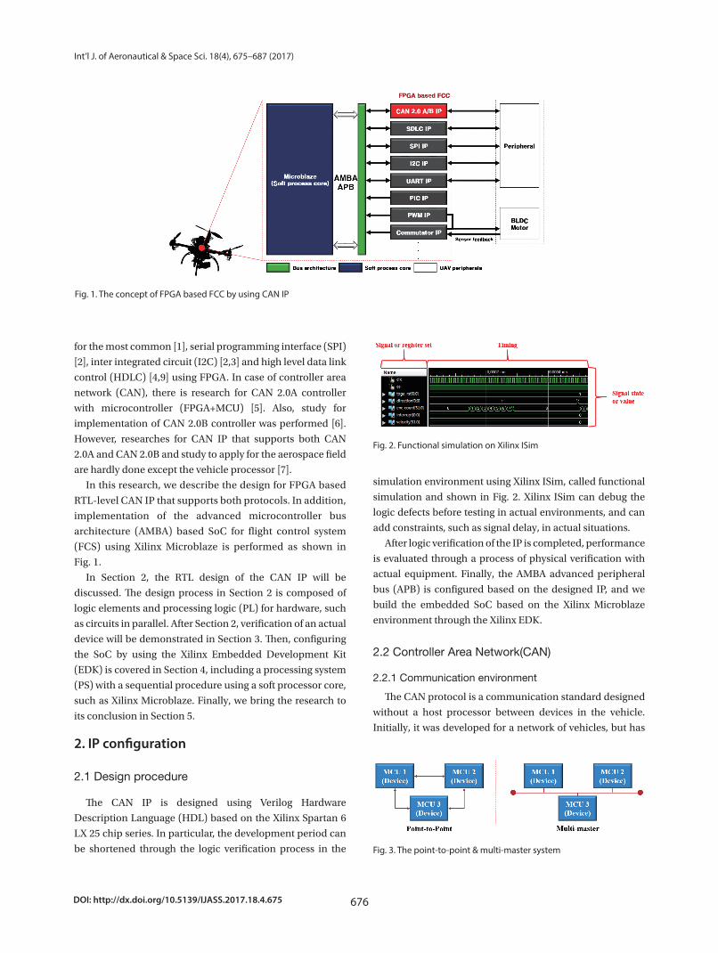
In this research, we describe the design for FPGA based
RTL-level CAN IP that supports both protocols. In addition,
implementation of the advanced microcontroller bus
architecture (AMBA) based SoC for flight control system
(FCS) using Xilinx Microblaze is performed as shown in
Fig. 1.
In Section 2, the RTL design of the CAN IP will be
discussed. The design process in Section 2 is composed of
logic elements and processing logic (PL) for hardware, such
as circuits in parallel. After Section 2, verification of an actual
device will be demonstrated in Section 3. Then, configuring
the SoC by using the Xilinx Embedded Development Kit
(EDK) is covered in Section 4, including a processing system
(PS) with a sequential procedure using a soft processor core,
such as Xilinx Microblaze. Finally, we bring the research to
its conclusion in Section 5.
2. IP configuration
2.1 Design procedure
The CAN IP is designed using Verilog Hardware
Description Language (HDL) based on the Xilinx Spartan 6
LX 25 chip series. In particular, the development period can
be shortened through the logic verification process in the
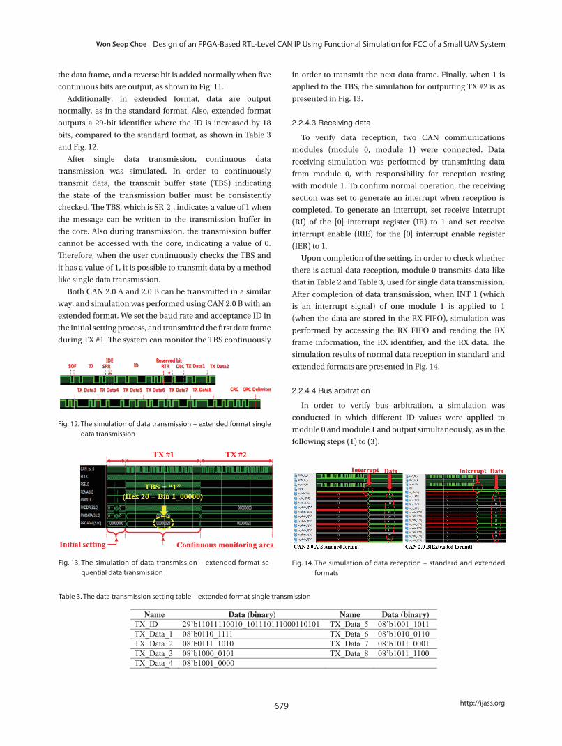
simulation environment using Xilinx ISim, called functional
simulation and shown in Fig. 2. Xilinx ISim can debug the
logic defects before testing in actual environments, and can
add constraints, such as signal delay, in actual situations.
After logic verification of the IP is completed, performance
is evaluated through a process of physical verification with
actual equipment. Finally, the AMBA advanced peripheral
bus (APB) is configured based on the designed IP, and we
build the embedded SoC based on the Xilinx Microblaze
environment through the Xilinx EDK.
2.2 Controller Area Network(CAN)
2.2.1 Communication environment
The CAN protocol is a communication standard designed
without a host processor between devices in the vehicle.
Initially, it was developed for a network of vehicles, but has
3
Fig. 1. The concept of FPGA based FCC by using CAN IP
In Section 2, the RTL design of the CAN IP will be discussed. The design process in Section 2 is
composed of logic elements and processing logic (PL) for hardware, such as circuits in parallel. After
Section 2, verification of an actual device will be demonstrated in Section 3. Then, configuring the
SoC by using the Xilinx Embedded Development Kit (EDK) is covered in Section 4, including a
processing system (PS) with a sequential procedure using a soft processor core, such as Xilinx
Microblaze. Finally, we bring the research to its conclusion in Section 5.
2. IP configuration
2.1 Design procedure
The CAN IP is designed using Verilog Hardware Description Language (HDL) based on the Xilinx
Spartan 6 LX 25 chip series. In particular, the development period can be shortened through the logic
verification process in the simulation environment using Xilinx ISim, called functional simulation and
shown in Fig. 2. Xilinx ISim can debug the logic defects before testing in actual environments, and
can add constraints, such as signal delay, in actual situations.
Fig. 2. Functional simulation on Xilinx ISim
Fig. 1. The concept of FPGA based FCC by using CAN IP
4
Fig. 3. Functional simulation on Xilinx ISim
After logic verification of the IP is completed, performance is evaluated through a process of
physical verification with actual equipment. Finally, the AMBA advanced peripheral bus (APB) is
configured based on the designed IP, and we build the embedded SoC based on the Xilinx Microblaze
environment through the Xilinx EDK.
2.2 Controller Area Network(CAN)
2.2.1 Communication environment
The CAN protocol is a communication standard designed without a host processor between devices
in the vehicle. Initially, it was developed for a network of vehicles, but has recently been widely
applied, not only to vehicles but also to all fields of industry, including aerospace. In the aerospace
field that includes UAVs, point-to-point communications like a universal asynchronous
receiver/transmitter (UART) between an MCU and devices requires a lot of wires, which directly
leads to complicated maintenance, increased weight, and lower mileage. A CAN increases
communications efficiency using the multi-master system shown in Fig. 3.
Fig. 3. The point-to-point & multi-master system
Fig. 2. Functional simulation on Xilinx ISim
4
Fig. 3. Functional simulation on Xilinx ISim
After logic verification of the IP is completed, performance is evaluated through a process of
physical verification with actual equipment. Finally, the AMBA advanced peripheral bus (APB) is
configured based on the designed IP, and we build the embedded SoC based on the Xilinx Microblaze
environment through the Xilinx EDK.
2.2 Controller Area Network(CAN)
2.2.1 Communication environment
The CAN protocol is a communication standard designed without a host processor between devices
in the vehicle. Initially, it was developed for a network of vehicles, but has recently been widely
applied, not only to vehicles but also to all fields of industry, including aerospace. In the aerospace
field that includes UAVs, point-to-point communications like a universal asynchronous
receiver/transmitter (UART) between an MCU and devices requires a lot of wires, which directly
leads to complicated maintenance, increased weight, and lower mileage. A CAN increases
communications efficiency using the multi-master system shown in Fig. 3.
Fig. 3. The point-to-point & multi-master system Fig. 3. The point-to-point & multi-master system
(675~687)2017-156.indd 676 2018-01-05 오후 8:42:12

677
Won Seop Choe Design of an FPGA-Based RTL-Level CAN IP Using Functional Simulation for FCC of a Small UAV System
http://ijass.org
recently been widely applied, not only to vehicles but also to
all fields of industry, including aerospace. In the aerospace
field that includes UAVs, point-to-point communications
like a universal asynchronous receiver/transmitter (UART)
between an MCU and devices requires a lot of wires, which
directly leads to complicated maintenance, increased weight,
and lower mileage. A CAN increases communications
efficiency using the multi-master system shown in Fig. 3.
2.2.2 Protocol compatibility
Generally, the CAN protocol is classified into two
categories, CAN 2.0A and CAN 2.0B. The CAN 2.0A has an
11-bit identifier according to the standard format. On the
other hand, CAN 2.0B which is an extended format has a 29-
bit identifier. Therefore, CAN 2.0A controller can transmit
and receive with the only standard format(CAN 2.0A), and
extended format(CAN 2.0B) can transmit and receive both
data formats. The critical compatibility problem between
both formats is that CAN 2.0A cannot receive data of CAN
2.0B as shown in Fig. 4.
In this paper, we designed a CAN IP to support both CAN
protocols with the goal of operating speeds up to 1 Mbps at
multi-master communication environment.
2.2.3 CAN IP configuration
The designed CAN IP consists of a baud rate prescaler, bit
timing logic, and a bit stream processor. The IP configuration
is shown in Fig. 5.
The baud rate prescaler receives the system clock and
generates the time quanta (TQ) corresponding to the time
units for CAN communications. Also, nominal bit time is
composed of tsync, tpropseg, and tps, as seen in Fig. 6, and each
element has operations (1) to (3), as follows. Sampling point
in nominal bit time can be adjusted by setting the bit time
logic.
(1) tsync: Notify the start of nominal bit time (1 TQ)
(2) tpropseg: Compensate for the physical delay between
CAN nodes (1-8 TQ)
(3) tps: Compensate for the edge phase error (2-8 TQ)
A bit stream processor was designed to perform functions
that include bit stream generating/de-generating, first in,
first out (FIFO), cyclical redundancy check (CRC), and
acceptance filter(ACF) as outlined in steps (1) to (5).
(1) Bit stream generator: Generate the data to be
transmitted to the frame structure.
(2) Bit stream de-generator: Input the bit from other nodes
at the sampling point and convert into data.
(3) FIFO: Consists of TX FIFO (108 bytes) and RX FIFO
(128 bytes).
(4) CRC: Use ordinary 15-bit CRC (x15+x14+x10+x8+x7+x4
+x3+1).
(5) Acceptance filter: Receive desired ID only by using
acceptance code and mask bit.
When the designed CAN IP receives the data, it checks the
validity of the data and stores the ID and information on the
8 bit register(Appendix A). Transmitting, also ID and data
are transmitted similar to physical CAN protocol controller
IC that carries out the contents specified in the CAN
communication such as buffer and control of data. However,
CAN IP designed on this research consists of logic elements
only, plays the same role as the physical protocol controller
as shown in Fig. 7.
6
The baud rate prescaler receives the system clock and generates the time quanta (TQ)
corresponding to the time units for CAN communications. Also, nominal bit time is composed of
, , and , as seen in Fig. 6, and each element has operations (1) to (3), as follows.
Sampling point in nominal bit time can be adjusted by setting the bit time logic.
Fig. 6. The sampling point at the nominal bit time
(1) : Notify the start of nominal bit time (1 TQ)
(2) : Compensate for the physical delay between CAN nodes (1-8 TQ)
(3) : Compensate for the edge phase error (2-8 TQ)
A bit stream processor was designed to perform functions that include bit stream generating/de-
generating, first in, first out (FIFO), cyclical redundancy check (CRC), and acceptance filter(ACF) as
outlined in steps (1) to (5).
(1) Bit stream generator: Generate the data to be transmitted to the frame structure.
(2) Bit stream de-generator: Input the bit from other nodes at the sampling point and convert into
data.
(3) FIFO: Consists of TX FIFO (108 bytes) and RX FIFO (128 bytes).
(4) CRC: Use ordinary 15-bit CRC ( + + + + + + +1).
(5) Acceptance filter: Receive desired ID only by using acceptance code and mask bit.
When the designed CAN IP receives the data, it checks the validity of the data and stores the ID
and information on the 8 bit register(Appendix A). Transmitting, also ID and data are transmitted
similar to physical CAN protocol controller IC that carries out the contents specified in the CAN
communication such as buffer and control of data. However, CAN IP designed on this research
consists of logic elements only, plays the same role as the physical protocol controller as shown in Fig.
7.
Fig. 6. The sampling point at the nominal bit time
7
Fig. 7. Key contribution of FPGA based CAN IP
Therefore, when designing CAN IP using FPGA, there is an advantage that physical elements can
be reduced. In addition, it is possible to implement the system intensively. Finally in the aerospace
industry field, the reduction in physical constraints as designed CAN IP is directly linked with the
performance of aircraft.
2.2.4 Logical verification using Xilinx ISim
Logical verification of the CAN IP was performed by using Xilinx ISim, a basic functional
simulator provided in the Xilinx ISE Design Suite. A total of eight main subjects required in the CAN
protocol were simulated and presented in the list below:
(1) Data bit setting
(2) Data transmission
(3) Receiving data
(4) Bus arbitration
(5) Error detection
(6) Acceptance filtering
2.2.4.1 Data bit setting
Simulation was performed with a 50 MHz clock and using about a 70~75% sampling point utilized
mainly by ordinary CAN communications through measured time of 1 bit SoF for a bit rate of 1000,
100, and 20. Also, bus timing registers(BTR0 and BTR1) of each bit rate are as seen in Table. 1.
BTR0 defines the value of the baud rate prescaler , BTR1 includes length of the bit period, the
location of the sampling point and the number of samples to be taken at each sampling point. Each
Fig. 7. Key contribution of FPGA based CAN IP5
2.2.2 Protocol compatibility
Generally, the CAN protocol is classified into two categories, CAN 2.0A and CAN 2.0B. The CAN
2.0A has an 11-bit identifier according to the standard format. On the other hand, CAN 2.0B which is
an extended format has a 29-bit identifier. Therefore, CAN 2.0A controller can transmit and receive
with the only standard format(CAN 2.0A), and extended format(CAN 2.0B) can transmit and receive
both data formats. The critical compatibility problem between both formats is that CAN 2.0A cannot
receive data of CAN 2.0B as shown in Fig. 4.
Fig. 4. Compatibility problem about CAN protocol
In this paper, we designed a CAN IP to support both CAN protocols with the goal of operating
speeds up to 1 Mbps at multi-master communication environment.
2.2.3 CAN IP configuration
The designed CAN IP consists of a baud rate prescaler, bit timing logic, and a bit stream processor.
The IP configuration is shown in Fig. 5.
Fig. 5. The CAN IP configuration and data vector
Fig. 4. Compatibility problem about CAN protocol
5
2.2.2 Protocol compatibility
Generally, the CAN protocol is classified into two categories, CAN 2.0A and CAN 2.0B. The CAN
2.0A has an 11-bit identifier according to the standard format. On the other hand, CAN 2.0B which is
an extended format has a 29-bit identifier. Therefore, CAN 2.0A controller can transmit and receive
with the only standard format(CAN 2.0A), and extended format(CAN 2.0B) can transmit and receive
both data formats. The critical compatibility problem between both formats is that CAN 2.0A cannot
receive data of CAN 2.0B as shown in Fig. 4.
Fig. 4. Compatibility problem about CAN protocol
In this paper, we designed a CAN IP to support both CAN protocols with the goal of operating
speeds up to 1 Mbps at multi-master communication environment.
2.2.3 CAN IP configuration
The designed CAN IP consists of a baud rate prescaler, bit timing logic, and a bit stream processor.
The IP configuration is shown in Fig. 5.
Fig. 5. The CAN IP configuration and data vector Fig. 5. The CAN IP configuration and data vector
4
Fig. 3. Functional simulation on Xilinx ISim
After logic verification of the IP is completed, performance is evaluated through a process of
physical verification with actual equipment. Finally, the AMBA advanced peripheral bus (APB) is
configured based on the designed IP, and we build the embedded SoC based on the Xilinx Microblaze
environment through the Xilinx EDK.
2.2 Controller Area Network(CAN)
2.2.1 Communication environment
The CAN protocol is a communication standard designed without a host processor between devices
in the vehicle. Initially, it was developed for a network of vehicles, but has recently been widely
applied, not only to vehicles but also to all fields of industry, including aerospace. In the aerospace
field that includes UAVs, point-to-point communications like a universal asynchronous
receiver/transmitter (UART) between an MCU and devices requires a lot of wires, which directly
leads to complicated maintenance, increased weight, and lower mileage. A CAN increases
communications efficiency using the multi-master system shown in Fig. 3.
Fig. 3. The point-to-point & multi-master system Fig. 3. The point-to-point & multi-master system
(675~687)2017-156.indd 677 2018-01-05 오후 8:42:13

DOI: http://dx.doi.org/10.5139/IJASS.2017.18.4.675 678
Int’l J. of Aeronautical & Space Sci. 18(4), 675–687 (2017)
Therefore, when designing CAN IP using FPGA, there is
an advantage that physical elements can be reduced. In
addition, it is possible to implement the system intensively.
Finally in the aerospace industry field, the reduction in
physical constraints as designed CAN IP is directly linked
with the performance of aircraft.
2.2.4 Logical verification using Xilinx ISim
Logical verification of the CAN IP was performed by using
Xilinx ISim, a basic functional simulator provided in the
Xilinx ISE Design Suite. A total of eight main subjects required
in the CAN protocol were simulated and presented in the list
below:
(1) Data bit setting
(2) Data transmission
(3) Receiving data
(4) Bus arbitration
(5) Error detection
(6) Acceptance filtering
2.2.4.1 Data bit setting
Simulation was performed with a 50 MHz clock and using
about a 70~75% sampling point utilized mainly by ordinary
CAN communications through measured time of 1 bit SoF for
a bit rate of 1000, 100, and 20. Also, bus timing registers(BTR0
and BTR1) of each bit rate are as seen in Table. 1. BTR0
defines the value of the baud rate prescaler, BTR1 includes
length of the bit period, the location of the sampling point
and the number of samples to be taken at each sampling
point. Each BTR is stored in address 6 and 7 on 8 bit CAN
register(Appendix A). Finally, it can be observed that the
SoF was correctly measured for each bit rate, except for a
measurement error of 0.6% at 20 Kbps, as shown in Fig. 8 to
Fig. 10.
2.2.4.2 Data transmission
It is necessary in the process to write the information of
the frame, the identifier, and the data to the FIFO transmitter
(TX) for data transmission. TX frame data (16th CAN address),
identifier (17th CAN address), upper-four-byte data (20th
CAN address) and lower-four-byte data (23th CAN address)
can be stored in FIFO. Data can be transferred by saving it in
the transmission FIFO and setting the transmission request
(TR) bit to 1 for data transfer. After setting the identifier and
data, like the lower part of Table 2, the simulation to analyze
the data of the standard format was carried out. It can be
confirmed that data are output according to the protocol of
Table 1. Bit rate table used in the bit-setting simulation
1
Table. 1. Bit rate table used in the bit-setting simulation
Bit rate Prescalar TQ Seg 1
Seg 2
Sampling point (%) BTR 0 BTR 1
1000 1 25 17 8 68.00 0x00 0x7f 100 12 21 16 5 76.19 0x0b 0x4e 20 54 23 17 6 73.91 0x35 0x5f
Table. 2. The data transmission setting table – standard format single transmission
Name Data (binary) Name Data (binary) TX_ID 11’b1100_0110_101 TX_Data_5 08’b0011_0111 TX_Data_1 08’b0000_1011 TX_Data_6 08’b0100_0010 TX_Data_2 08’b0001_0110 TX_Data_7 08’b0100_1101 TX_Data_3 08’b0010_0001 TX_Data_8 08’b0101_1000 TX_Data_4 08’b0010_1100
Table. 3. The data transmission setting table – extended format single transmission
Name Data (binary) Name Data (binary) TX_ID 29’b11011110010_101110111000110101 TX_Data_5 08’b1001_1011 TX_Data_1 08’b0110_1111 TX_Data_6 08’b1010_0110 TX_Data_2 08’b0111_1010 TX_Data_7 08’b1011_0001 TX_Data_3 08’b1000_0101 TX_Data_8 08’b1011_1100 TX_Data_4 08’b1001_0000
Table. 4. Module ID table – between standard formats (2.0A data, 2.0A data → CAN IP)
Module number ID (binary) Module 0 11’b1100_0110_101 Module 1 11’b1100_0110_011
Table. 5. Module ID table between extended formats (2.0B data, 2.0B data → CAN IP)
Module number ID (binary) ID (decimal) Module 0 29’b11011110010_101110111000110101 29’d466284085 Module 1 29’b11011110010_101110011011010110 29’d466282198
Table. 6. Module ID table between standard format and extended format (2.0A data, 2.0B data → CAN IP)
Module number ID (binary) Module 0 11’b11000110101 Module 1 29’b11011110010_101110011011010110
8
BTR is stored in address 6 and 7 on 8 bit CAN register(Appendix A). Finally, it can be observed that
the SoF was correctly measured for each bit rate, except for a measurement error of 0.6% at 20 Kbps,
as shown in Fig. 8 to Fig. 10.
Table. 1. Bit rate table used in the bit-setting simulation
Bit rate Prescalar TQ Seg 1
Seg 2
Sampling point (%) BTR 0 BTR 1
1000 1 25 17 8 68.00 0x00 0x7f 100 12 21 16 5 76.19 0x0b 0x4e 20 54 23 17 6 73.91 0x35 0x5f
Fig. 8. SoF measurement at a bit rate of 1000 Kbps
Fig. 9. SoF measurement at a bit rate of 100 Kbps
Fig. 10. SoF measurement at a bit rate of 20 Kbps
2.2.4.2 Data transmission
It is necessary in the process to write the information of the frame, the identifier, and the data to the
FIFO transmitter (TX) for data transmission. TX frame data (16th CAN address), identifier (17th CAN
address), upper-four-byte data (20th CAN address) and lower-four-byte data (23th CAN address) can
be stored in FIFO. Data can be transferred by saving it in the transmission FIFO and setting the
transmission request (TR) bit to 1 for data transfer. After setting the identifier and data, like the lower
part of Table 2, the simulation to analyze the data of the standard format was carried out. It can be
confirmed that data are output according to the protocol of the data frame, and a reverse bit is added
Fig. 8. SoF measurement at a bit rate of 1000 Kbps
8
BTR is stored in address 6 and 7 on 8 bit CAN register(Appendix A). Finally, it can be observed that
the SoF was correctly measured for each bit rate, except for a measurement error of 0.6% at 20 Kbps,
as shown in Fig. 8 to Fig. 10.
Table. 1. Bit rate table used in the bit-setting simulation
Bit rate Prescalar TQ Seg 1
Seg 2
Sampling point (%) BTR 0 BTR 1
1000 1 25 17 8 68.00 0x00 0x7f 100 12 21 16 5 76.19 0x0b 0x4e 20 54 23 17 6 73.91 0x35 0x5f
Fig. 8. SoF measurement at a bit rate of 1000 Kbps
Fig. 9. SoF measurement at a bit rate of 100 Kbps
Fig. 10. SoF measurement at a bit rate of 20 Kbps
2.2.4.2 Data transmission
It is necessary in the process to write the information of the frame, the identifier, and the data to the
FIFO transmitter (TX) for data transmission. TX frame data (16th CAN address), identifier (17th CAN
address), upper-four-byte data (20th CAN address) and lower-four-byte data (23th CAN address) can
be stored in FIFO. Data can be transferred by saving it in the transmission FIFO and setting the
transmission request (TR) bit to 1 for data transfer. After setting the identifier and data, like the lower
part of Table 2, the simulation to analyze the data of the standard format was carried out. It can be
confirmed that data are output according to the protocol of the data frame, and a reverse bit is added
Fig. 9. SoF measurement at a bit rate of 100 Kbps
8
BTR is stored in address 6 and 7 on 8 bit CAN register(Appendix A). Finally, it can be observed that
the SoF was correctly measured for each bit rate, except for a measurement error of 0.6% at 20 Kbps,
as shown in Fig. 8 to Fig. 10.
Table. 1. Bit rate table used in the bit-setting simulation
Bit rate Prescalar TQ Seg 1
Seg 2
Sampling point (%) BTR 0 BTR 1
1000 1 25 17 8 68.00 0x00 0x7f 100 12 21 16 5 76.19 0x0b 0x4e 20 54 23 17 6 73.91 0x35 0x5f
Fig. 8. SoF measurement at a bit rate of 1000 Kbps
Fig. 9. SoF measurement at a bit rate of 100 Kbps
Fig. 10. SoF measurement at a bit rate of 20 Kbps
2.2.4.2 Data transmission
It is necessary in the process to write the information of the frame, the identifier, and the data to the
FIFO transmitter (TX) for data transmission. TX frame data (16th CAN address), identifier (17th CAN
address), upper-four-byte data (20th CAN address) and lower-four-byte data (23th CAN address) can
be stored in FIFO. Data can be transferred by saving it in the transmission FIFO and setting the
transmission request (TR) bit to 1 for data transfer. After setting the identifier and data, like the lower
part of Table 2, the simulation to analyze the data of the standard format was carried out. It can be
confirmed that data are output according to the protocol of the data frame, and a reverse bit is added
Fig. 10. SoF measurement at a bit rate of 20 Kbps
Table 2. The data transmission setting table – standard format single transmission
1
Table. 1. Bit rate table used in the bit-setting simulation
Bit rate Prescalar TQ Seg 1
Seg 2
Sampling point (%) BTR 0 BTR 1
1000 1 25 17 8 68.00 0x00 0x7f 100 12 21 16 5 76.19 0x0b 0x4e 20 54 23 17 6 73.91 0x35 0x5f
Table. 2. The data transmission setting table – standard format single transmission
Name Data (binary) Name Data (binary) TX_ID 11’b1100_0110_101 TX_Data_5 08’b0011_0111 TX_Data_1 08’b0000_1011 TX_Data_6 08’b0100_0010 TX_Data_2 08’b0001_0110 TX_Data_7 08’b0100_1101 TX_Data_3 08’b0010_0001 TX_Data_8 08’b0101_1000 TX_Data_4 08’b0010_1100
Table. 3. The data transmission setting table – extended format single transmission
Name Data (binary) Name Data (binary) TX_ID 29’b11011110010_101110111000110101 TX_Data_5 08’b1001_1011 TX_Data_1 08’b0110_1111 TX_Data_6 08’b1010_0110 TX_Data_2 08’b0111_1010 TX_Data_7 08’b1011_0001 TX_Data_3 08’b1000_0101 TX_Data_8 08’b1011_1100 TX_Data_4 08’b1001_0000
Table. 4. Module ID table – between standard formats (2.0A data, 2.0A data → CAN IP)
Module number ID (binary) Module 0 11’b1100_0110_101 Module 1 11’b1100_0110_011
Table. 5. Module ID table between extended formats (2.0B data, 2.0B data → CAN IP)
Module number ID (binary) ID (decimal) Module 0 29’b11011110010_101110111000110101 29’d466284085 Module 1 29’b11011110010_101110011011010110 29’d466282198
Table. 6. Module ID table between standard format and extended format (2.0A data, 2.0B data → CAN IP)
Module number ID (binary) Module 0 11’b11000110101 Module 1 29’b11011110010_101110011011010110
9
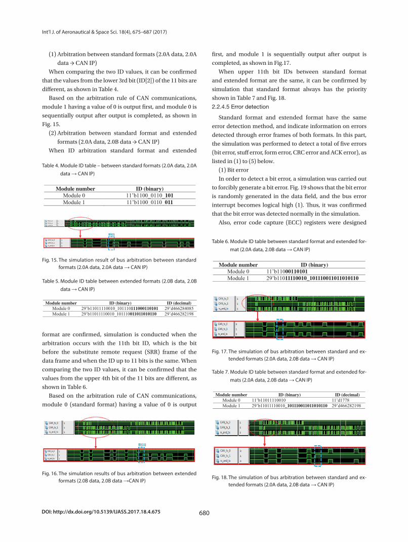
normally when five continuous bits are output, as shown in Fig. 11.
Table. 2. The data transmission setting table – standard format single transmission
Name Data (binary) Name Data (binary) TX_ID 11’b1100_0110_101 TX_Data_5 08’b0011_0111 TX_Data_1 08’b0000_1011 TX_Data_6 08’b0100_0010 TX_Data_2 08’b0001_0110 TX_Data_7 08’b0100_1101 TX_Data_3 08’b0010_0001 TX_Data_8 08’b0101_1000 TX_Data_4 08’b0010_1100
Fig. 11. The simulation of data transmission – standard format single data transmission
Additionally, in extended format, data are output normally, as in the standard format. Also,
extended format outputs a 29-bit identifier where the ID is increased by 18 bits, compared to the
standard format, as shown in Table 3 and Fig. 12.
Table. 3. The data transmission setting table – extended format single transmission
Name Data (binary) Name Data (binary) TX_ID 29’b11011110010_101110111000110101 TX_Data_5 08’b1001_1011 TX_Data_1 08’b0110_1111 TX_Data_6 08’b1010_0110 TX_Data_2 08’b0111_1010 TX_Data_7 08’b1011_0001 TX_Data_3 08’b1000_0101 TX_Data_8 08’b1011_1100 TX_Data_4 08’b1001_0000
Fig. 12. The simulation of data transmission – extended format single data transmission
After single data transmission, continuous data transmission was simulated. In order to
continuously transmit data, the transmit buffer state (TBS) indicating the state of the transmission
buffer must be consistently checked. The TBS, which is SR[2], indicates a value of 1 when the
Fig. 11. The simulation of data transmission – standard format single data transmission
(675~687)2017-156.indd 678 2018-01-05 오후 8:42:13
679
Won Seop Choe Design of an FPGA-Based RTL-Level CAN IP Using Functional Simulation for FCC of a Small UAV System
http://ijass.org
the data frame, and a reverse bit is added normally when five
continuous bits are output, as shown in Fig. 11.
Additionally, in extended format, data are output
normally, as in the standard format. Also, extended format
outputs a 29-bit identifier where the ID is increased by 18
bits, compared to the standard format, as shown in Table 3
and Fig. 12.
After single data transmission, continuous data
transmission was simulated. In order to continuously
transmit data, the transmit buffer state (TBS) indicating
the state of the transmission buffer must be consistently
checked. The TBS, which is SR[2], indicates a value of 1 when
the message can be written to the transmission buffer in
the core. Also during transmission, the transmission buffer
cannot be accessed with the core, indicating a value of 0.
Therefore, when the user continuously checks the TBS and
it has a value of 1, it is possible to transmit data by a method
like single data transmission.
Both CAN 2.0 A and 2.0 B can be transmitted in a similar
way, and simulation was performed using CAN 2.0 B with an
extended format. We set the baud rate and acceptance ID in
the initial setting process, and transmitted the first data frame
during TX #1. The system can monitor the TBS continuously
in order to transmit the next data frame. Finally, when 1 is
applied to the TBS, the simulation for outputting TX #2 is as
presented in Fig. 13.
2.2.4.3 Receiving data
To verify data reception, two CAN communications
modules (module 0, module 1) were connected. Data
receiving simulation was performed by transmitting data
from module 0, with responsibility for reception resting
with module 1. To confirm normal operation, the receiving
section was set to generate an interrupt when reception is
completed. To generate an interrupt, set receive interrupt
(RI) of the [0] interrupt register (IR) to 1 and set receive
interrupt enable (RIE) for the [0] interrupt enable register
(IER) to 1.
Upon completion of the setting, in order to check whether
there is actual data reception, module 0 transmits data like
that in Table 2 and Table 3, used for single data transmission.
After completion of data transmission, when INT 1 (which
is an interrupt signal) of one module 1 is applied to 1
(when the data are stored in the RX FIFO), simulation was
performed by accessing the RX FIFO and reading the RX
frame information, the RX identifier, and the RX data. The
simulation results of normal data reception in standard and
extended formats are presented in Fig. 14.
2.2.4.4 Bus arbitration
In order to verify bus arbitration, a simulation was
conducted in which different ID values were applied to
module 0 and module 1 and output simultaneously, as in the
following steps (1) to (3).
Table 3. The data transmission setting table – extended format single transmission
1
Table. 1. Bit rate table used in the bit-setting simulation
Bit rate Prescalar TQ Seg 1
Seg 2
Sampling point (%) BTR 0 BTR 1
1000 1 25 17 8 68.00 0x00 0x7f 100 12 21 16 5 76.19 0x0b 0x4e 20 54 23 17 6 73.91 0x35 0x5f
Table. 2. The data transmission setting table – standard format single transmission
Name Data (binary) Name Data (binary) TX_ID 11’b1100_0110_101 TX_Data_5 08’b0011_0111 TX_Data_1 08’b0000_1011 TX_Data_6 08’b0100_0010 TX_Data_2 08’b0001_0110 TX_Data_7 08’b0100_1101 TX_Data_3 08’b0010_0001 TX_Data_8 08’b0101_1000 TX_Data_4 08’b0010_1100
Table. 3. The data transmission setting table – extended format single transmission
Name Data (binary) Name Data (binary) TX_ID 29’b11011110010_101110111000110101 TX_Data_5 08’b1001_1011 TX_Data_1 08’b0110_1111 TX_Data_6 08’b1010_0110 TX_Data_2 08’b0111_1010 TX_Data_7 08’b1011_0001 TX_Data_3 08’b1000_0101 TX_Data_8 08’b1011_1100 TX_Data_4 08’b1001_0000
Table. 4. Module ID table – between standard formats (2.0A data, 2.0A data → CAN IP)
Module number ID (binary) Module 0 11’b1100_0110_101 Module 1 11’b1100_0110_011
Table. 5. Module ID table between extended formats (2.0B data, 2.0B data → CAN IP)
Module number ID (binary) ID (decimal) Module 0 29’b11011110010_101110111000110101 29’d466284085 Module 1 29’b11011110010_101110011011010110 29’d466282198
Table. 6. Module ID table between standard format and extended format (2.0A data, 2.0B data → CAN IP)
Module number ID (binary) Module 0 11’b11000110101 Module 1 29’b11011110010_101110011011010110
9
normally when five continuous bits are output, as shown in Fig. 11.
Table. 2. The data transmission setting table – standard format single transmission
Name Data (binary) Name Data (binary) TX_ID 11’b1100_0110_101 TX_Data_5 08’b0011_0111 TX_Data_1 08’b0000_1011 TX_Data_6 08’b0100_0010 TX_Data_2 08’b0001_0110 TX_Data_7 08’b0100_1101 TX_Data_3 08’b0010_0001 TX_Data_8 08’b0101_1000 TX_Data_4 08’b0010_1100
Fig. 11. The simulation of data transmission – standard format single data transmission
Additionally, in extended format, data are output normally, as in the standard format. Also,
extended format outputs a 29-bit identifier where the ID is increased by 18 bits, compared to the
standard format, as shown in Table 3 and Fig. 12.
Table. 3. The data transmission setting table – extended format single transmission
Name Data (binary) Name Data (binary) TX_ID 29’b11011110010_101110111000110101 TX_Data_5 08’b1001_1011 TX_Data_1 08’b0110_1111 TX_Data_6 08’b1010_0110 TX_Data_2 08’b0111_1010 TX_Data_7 08’b1011_0001 TX_Data_3 08’b1000_0101 TX_Data_8 08’b1011_1100 TX_Data_4 08’b1001_0000
Fig. 12. The simulation of data transmission – extended format single data transmission
After single data transmission, continuous data transmission was simulated. In order to
continuously transmit data, the transmit buffer state (TBS) indicating the state of the transmission
buffer must be consistently checked. The TBS, which is SR[2], indicates a value of 1 when the
Fig. 12. The simulation of data transmission – extended format single data transmission
10
message can be written to the transmission buffer in the core. Also during transmission, the
transmission buffer cannot be accessed with the core, indicating a value of 0. Therefore, when the user
continuously checks the TBS and it has a value of 1, it is possible to transmit data by a method like
single data transmission.
Both CAN 2.0 A and 2.0 B can be transmitted in a similar way, and simulation was performed using
CAN 2.0 B with an extended format. We set the baud rate and acceptance ID in the initial setting
process, and transmitted the first data frame during TX #1. The system can monitor the TBS
continuously in order to transmit the next data frame. Finally, when 1 is applied to the TBS, the
simulation for outputting TX #2 is as presented in Fig. 13.
Fig. 13. The simulation of data transmission – extended format sequential data transmission
2.2.4.3 Receiving data
To verify data reception, two CAN communications modules (module 0, module 1) were connected.
Data receiving simulation was performed by transmitting data from module 0, with responsibility for
reception resting with module 1. To confirm normal operation, the receiving section was set to
generate an interrupt when reception is completed. To generate an interrupt, set receive interrupt (RI)
of the [0] interrupt register (IR) to 1 and set receive interrupt enable (RIE) for the [0] interrupt enable
register (IER) to 1.
Upon completion of the setting, in order to check whether there is actual data reception, module 0
transmits data like that in Table 2 and Table 3, used for single data transmission. After completion of
data transmission, when INT 1 (which is an interrupt signal) of one module 1 is applied to 1 (when the
Fig. 13. The simulation of data transmission – extended format se-quential data transmission
11
data are stored in the RX FIFO), simulation was performed by accessing the RX FIFO and reading the
RX frame information, the RX identifier, and the RX data. The simulation results of normal data
reception in standard and extended formats are presented in Fig. 14.
Fig. 14. The simulation of data reception – standard and extended formats
2.2.4.4 Bus arbitration
In order to verify bus arbitration, a simulation was conducted in which different ID values were
applied to module 0 and module 1 and output simultaneously, as in the following steps (1) to (3).
(1) Arbitration between standard formats (2.0A data, 2.0A data → CAN IP)
When comparing the two ID values, it can be confirmed that the values from the lower 3rd bit
(ID[2]) of the 11 bits are different, as shown in Table 4.
Table. 4. Module ID table – between standard formats (2.0A data, 2.0A data → CAN IP)
Module number ID (binary) Module 0 11’b1100_0110_101 Module 1 11’b1100_0110_011
Based on the arbitration rule of CAN communications, module 1 having a value of 0 is
output first, and module 0 is sequentially output after output is completed, as shown in Fig. 15.
Fig. 14. The simulation of data reception – standard and extended formats
(675~687)2017-156.indd 679 2018-01-05 오후 8:42:14
DOI: http://dx.doi.org/10.5139/IJASS.2017.18.4.675 680
Int’l J. of Aeronautical & Space Sci. 18(4), 675–687 (2017)
(1) Arbitration between standard formats (2.0A data, 2.0A
data → CAN IP)
When comparing the two ID values, it can be confirmed
that the values from the lower 3rd bit (ID[2]) of the 11 bits are
different, as shown in Table 4.
Based on the arbitration rule of CAN communications,
module 1 having a value of 0 is output first, and module 0 is
sequentially output after output is completed, as shown in
Fig. 15.
(2) Arbitration between standard format and extended
formats (2.0A data, 2.0B data → CAN IP)
When ID arbitration standard format and extended
format are confirmed, simulation is conducted when the
arbitration occurs with the 11th bit ID, which is the bit
before the substitute remote request (SRR) frame of the
data frame and when the ID up to 11 bits is the same. When
comparing the two ID values, it can be confirmed that the
values from the upper 4th bit of the 11 bits are different, as
shown in Table 6.
Based on the arbitration rule of CAN communications,
module 0 (standard format) having a value of 0 is output
first, and module 1 is sequentially output after output is
completed, as shown in Fig.17.
When upper 11th bit IDs between standard format
and extended format are the same, it can be confirmed by
simulation that standard format always has the priority
shown in Table 7 and Fig. 18.
2.2.4.5 Error detection
Standard format and extended format have the same
error detection method, and indicate information on errors
detected through error frames of both formats. In this part,
the simulation was performed to detect a total of five errors
(bit error, stuff error, form error, CRC error and ACK error), as
listed in (1) to (5) below.
(1) Bit error
In order to detect a bit error, a simulation was carried out
to forcibly generate a bit error. Fig. 19 shows that the bit error
is randomly generated in the data field, and the bus error
interrupt becomes logical high (1). Thus, it was confirmed
that the bit error was detected normally in the simulation.
Also, error code capture (ECC) registers were designed
Table 4. Module ID table – between standard formats (2.0A data, 2.0A data → CAN IP)
1
Table. 1. Bit rate table used in the bit-setting simulation
Bit rate Prescalar TQ Seg 1
Seg 2
Sampling point (%) BTR 0 BTR 1
1000 1 25 17 8 68.00 0x00 0x7f 100 12 21 16 5 76.19 0x0b 0x4e 20 54 23 17 6 73.91 0x35 0x5f
Table. 2. The data transmission setting table – standard format single transmission
Name Data (binary) Name Data (binary) TX_ID 11’b1100_0110_101 TX_Data_5 08’b0011_0111 TX_Data_1 08’b0000_1011 TX_Data_6 08’b0100_0010 TX_Data_2 08’b0001_0110 TX_Data_7 08’b0100_1101 TX_Data_3 08’b0010_0001 TX_Data_8 08’b0101_1000 TX_Data_4 08’b0010_1100
Table. 3. The data transmission setting table – extended format single transmission
Name Data (binary) Name Data (binary) TX_ID 29’b11011110010_101110111000110101 TX_Data_5 08’b1001_1011 TX_Data_1 08’b0110_1111 TX_Data_6 08’b1010_0110 TX_Data_2 08’b0111_1010 TX_Data_7 08’b1011_0001 TX_Data_3 08’b1000_0101 TX_Data_8 08’b1011_1100 TX_Data_4 08’b1001_0000
Table. 4. Module ID table – between standard formats (2.0A data, 2.0A data → CAN IP)
Module number ID (binary) Module 0 11’b1100_0110_101 Module 1 11’b1100_0110_011
Table. 5. Module ID table between extended formats (2.0B data, 2.0B data → CAN IP)
Module number ID (binary) ID (decimal) Module 0 29’b11011110010_101110111000110101 29’d466284085 Module 1 29’b11011110010_101110011011010110 29’d466282198
Table. 6. Module ID table between standard format and extended format (2.0A data, 2.0B data → CAN IP)
Module number ID (binary) Module 0 11’b11000110101 Module 1 29’b11011110010_101110011011010110
Table 5. Module ID table between extended formats (2.0B data, 2.0B data → CAN IP)
1
Table. 1. Bit rate table used in the bit-setting simulation
Bit rate Prescalar TQ Seg 1
Seg 2
Sampling point (%) BTR 0 BTR 1
1000 1 25 17 8 68.00 0x00 0x7f 100 12 21 16 5 76.19 0x0b 0x4e 20 54 23 17 6 73.91 0x35 0x5f
Table. 2. The data transmission setting table – standard format single transmission
Name Data (binary) Name Data (binary) TX_ID 11’b1100_0110_101 TX_Data_5 08’b0011_0111 TX_Data_1 08’b0000_1011 TX_Data_6 08’b0100_0010 TX_Data_2 08’b0001_0110 TX_Data_7 08’b0100_1101 TX_Data_3 08’b0010_0001 TX_Data_8 08’b0101_1000 TX_Data_4 08’b0010_1100
Table. 3. The data transmission setting table – extended format single transmission
Name Data (binary) Name Data (binary) TX_ID 29’b11011110010_101110111000110101 TX_Data_5 08’b1001_1011 TX_Data_1 08’b0110_1111 TX_Data_6 08’b1010_0110 TX_Data_2 08’b0111_1010 TX_Data_7 08’b1011_0001 TX_Data_3 08’b1000_0101 TX_Data_8 08’b1011_1100 TX_Data_4 08’b1001_0000
Table. 4. Module ID table – between standard formats (2.0A data, 2.0A data → CAN IP)
Module number ID (binary) Module 0 11’b1100_0110_101 Module 1 11’b1100_0110_011
Table. 5. Module ID table between extended formats (2.0B data, 2.0B data → CAN IP)
Module number ID (binary) ID (decimal) Module 0 29’b11011110010_101110111000110101 29’d466284085 Module 1 29’b11011110010_101110011011010110 29’d466282198
Table. 6. Module ID table between standard format and extended format (2.0A data, 2.0B data → CAN IP)
Module number ID (binary) Module 0 11’b11000110101 Module 1 29’b11011110010_101110011011010110
11
data are stored in the RX FIFO), simulation was performed by accessing the RX FIFO and reading the
RX frame information, the RX identifier, and the RX data. The simulation results of normal data
reception in standard and extended formats are presented in Fig. 14.
Fig. 14. The simulation of data reception – standard and extended formats
2.2.4.4 Bus arbitration
In order to verify bus arbitration, a simulation was conducted in which different ID values were
applied to module 0 and module 1 and output simultaneously, as in the following steps (1) to (3).
(1) Arbitration between standard formats (2.0A data, 2.0A data → CAN IP)
When comparing the two ID values, it can be confirmed that the values from the lower 3rd bit
(ID[2]) of the 11 bits are different, as shown in Table 4.
Table. 4. Module ID table – between standard formats (2.0A data, 2.0A data → CAN IP)
Module number ID (binary) Module 0 11’b1100_0110_101 Module 1 11’b1100_0110_011
Based on the arbitration rule of CAN communications, module 1 having a value of 0 is
output first, and module 0 is sequentially output after output is completed, as shown in Fig. 15.
Fig. 15. The simulation result of bus arbitration between standard formats (2.0A data, 2.0A data → CAN IP)
12
Fig. 15. The simulation result of bus arbitration between standard formats (2.0A data, 2.0A data → CAN IP)
(2) Arbitration between extended formats (2.0B data, 2.0B data → CAN IP)
Extended format simulation is executed to confirm ID arbitration, and module 1 is
transmitted first from ID[11] by the arbitration rule, as shown in Table 5 and Fig. 16.
Table. 5. Module ID table between extended formats (2.0B data, 2.0B data → CAN IP)
Module number ID (binary) ID (decimal) Module 0 29’b11011110010_101110111000110101 29’d466284085 Module 1 29’b11011110010_101110011011010110 29’d466282198
Fig. 16. The simulation results of bus arbitration between extended formats (2.0B data, 2.0B data → CAN IP)
(3) Arbitration between standard format and extended formats (2.0A data, 2.0B data → CAN IP)
When ID arbitration standard format and extended format are confirmed, simulation is
conducted when the arbitration occurs with the 11th bit ID, which is the bit before the substitute
remote request (SRR) frame of the data frame and when the ID up to 11 bits is the same. When
comparing the two ID values, it can be confirmed that the values from the upper 4th bit of the 11
bits are different, as shown in Table 6.
Table. 6. Module ID table between standard format and extended format (2.0A data, 2.0B data → CAN IP)
Module number ID (binary) Module 0 11’b11000110101 Module 1 29’b11011110010_101110011011010110
Based on the arbitration rule of CAN communications, module 0 (standard format) having a
value of 0 is output first, and module 1 is sequentially output after output is completed, as
shown in Fig.17.
Fig. 16. The simulation results of bus arbitration between extended formats (2.0B data, 2.0B data →CAN IP)
Table 6. Module ID table between standard format and extended for-mat (2.0A data, 2.0B data → CAN IP)
1
Table. 1. Bit rate table used in the bit-setting simulation
Bit rate Prescalar TQ Seg 1
Seg 2
Sampling point (%) BTR 0 BTR 1
1000 1 25 17 8 68.00 0x00 0x7f 100 12 21 16 5 76.19 0x0b 0x4e 20 54 23 17 6 73.91 0x35 0x5f
Table. 2. The data transmission setting table – standard format single transmission
Name Data (binary) Name Data (binary) TX_ID 11’b1100_0110_101 TX_Data_5 08’b0011_0111 TX_Data_1 08’b0000_1011 TX_Data_6 08’b0100_0010 TX_Data_2 08’b0001_0110 TX_Data_7 08’b0100_1101 TX_Data_3 08’b0010_0001 TX_Data_8 08’b0101_1000 TX_Data_4 08’b0010_1100
Table. 3. The data transmission setting table – extended format single transmission
Name Data (binary) Name Data (binary) TX_ID 29’b11011110010_101110111000110101 TX_Data_5 08’b1001_1011 TX_Data_1 08’b0110_1111 TX_Data_6 08’b1010_0110 TX_Data_2 08’b0111_1010 TX_Data_7 08’b1011_0001 TX_Data_3 08’b1000_0101 TX_Data_8 08’b1011_1100 TX_Data_4 08’b1001_0000
Table. 4. Module ID table – between standard formats (2.0A data, 2.0A data → CAN IP)
Module number ID (binary) Module 0 11’b1100_0110_101 Module 1 11’b1100_0110_011
Table. 5. Module ID table between extended formats (2.0B data, 2.0B data → CAN IP)
Module number ID (binary) ID (decimal) Module 0 29’b11011110010_101110111000110101 29’d466284085 Module 1 29’b11011110010_101110011011010110 29’d466282198
Table. 6. Module ID table between standard format and extended format (2.0A data, 2.0B data → CAN IP)
Module number ID (binary) Module 0 11’b11000110101 Module 1 29’b11011110010_101110011011010110
Table 7. Module ID table between standard format and extended for-mats (2.0A data, 2.0B data → CAN IP)
2
Table. 7. Module ID table between standard format and extended formats (2.0A data, 2.0B data → CAN IP)
Module number ID (binary) ID (decimal) Module 0 11’b11011110010 11’d1778 Module 1 29’b11011110010_101110011011010110 29’d466282198
Table. 8. ECC register information on bit errors
ECC reg Signal name Value Classification ECC [7:6] Errc_0 0 Bit error ECC [5] Error_dir_0 0 Error during transmission ECC [4:0] Error_segment_0 01010 Error at data field
Table. 9. ECC register information on the stuff error
ECC reg Signal name Value Classification ECC [7:6] Errc_1 10 Stuff error ECC [5] Error_dir_1 1 Error during receiving ECC [4:0] Error_segment_1 01010 Error at data field
Table. 10. ECC register information on form error
ECC reg Signal name Value Classification ECC [7:6] Errc_1 01 Form error ECC [5] Error_dir_1 1 Error during receiving ECC [4:0] Error_segment_1 011000 Error at CRC delimiter
Table. 11. ECC register information on the CRC error
ECC reg Signal name Value Classification ECC [7:6] Errc_1 11 Other error ECC [5] Error_dir_1 1 Error during receiving ECC [4:0] Error_segment_1 11001 Error at acknowledge slot
Table. 12. ECC register information on the ACK error
ECC reg Signal name Value Classification ECC [7:6] Errc_0 11 Other error ECC [5] Error_dir_0 0 Error during transmission ECC [4:0] Error_segment_0 11001 Error at acknowledge slot
13
Fig. 17. The simulation of bus arbitration between standard and extended formats (2.0A data, 2.0B data → CAN IP)
When upper 11th bit IDs between standard format and extended format are the same, it can be
confirmed by simulation that standard format always has the priority shown in Table 7 and
Fig. 18.
Table. 7. Module ID table between standard format and extended formats (2.0A data, 2.0B data → CAN IP)
Module number ID (binary) ID (decimal) Module 0 11’b11011110010 11’d1778 Module 1 29’b11011110010_101110011011010110 29’d466282198
Fig. 18. The simulation of bus arbitration between standard and extended formats (2.0A data, 2.0B data → CAN IP)
2.2.4.5 Error detection
Standard format and extended format have the same error detection method, and indicate
information on errors detected through error frames of both formats. In this part, the simulation was
performed to detect a total of five errors (bit error, stuff error, form error, CRC error and ACK error),
as listed in (1) to (5) below.
(1) Bit error
In order to detect a bit error, a simulation was carried out to forcibly generate a bit error.
Fig. 17. The simulation of bus arbitration between standard and ex-tended formats (2.0A data, 2.0B data → CAN IP)
13
Fig. 17. The simulation of bus arbitration between standard and extended formats (2.0A data, 2.0B data → CAN IP)
When upper 11th bit IDs between standard format and extended format are the same, it can be
confirmed by simulation that standard format always has the priority shown in Table 7 and
Fig. 18.
Table. 7. Module ID table between standard format and extended formats (2.0A data, 2.0B data → CAN IP)
Module number ID (binary) ID (decimal) Module 0 11’b11011110010 11’d1778 Module 1 29’b11011110010_101110011011010110 29’d466282198
Fig. 18. The simulation of bus arbitration between standard and extended formats (2.0A data, 2.0B data → CAN IP)
2.2.4.5 Error detection
Standard format and extended format have the same error detection method, and indicate
information on errors detected through error frames of both formats. In this part, the simulation was
performed to detect a total of five errors (bit error, stuff error, form error, CRC error and ACK error),
as listed in (1) to (5) below.
(1) Bit error
In order to detect a bit error, a simulation was carried out to forcibly generate a bit error.
Fig. 18. The simulation of bus arbitration between standard and ex-tended formats (2.0A data, 2.0B data → CAN IP)
(675~687)2017-156.indd 680 2018-01-05 오후 8:42:15
681
Won Seop Choe Design of an FPGA-Based RTL-Level CAN IP Using Functional Simulation for FCC of a Small UAV System
http://ijass.org
for capturing the error information using error capture. The
captured error information is seen in Table 8.
(2) Stuff error
This occurs when the values of six consecutive bits are on
the bus. In order to confirm error detection, we sent a bit that
outputs 5 or more 0’s to the bus node (rx_and_tx). As a result
of simulation, stuff error was detected on the receiving side,
and a bus error interrupt was generated normally, as shown
in Fig. 20, and ECC register information on the stuff error is
represented in Table 9.
A bit signal of 1 is determined for a CRC delimiter, an ACK
delimiter, and EoF. The form error occurs when breaking
that rule. In order to confirm error detection, a simulation
was performed with the CRC delimiter set to 0. When the
form rule is corrupted, as shown in Fig. 21, it can be known
that the interrupt is normally generated. Also, ECC register
information on the form error is shown in Table 10.
(4) CRC error
Forcibly reverse the 1 bit of the CRC sent in the simulation
to detect a CRC error. As a result, an error occurs after the
CRC is completed, an error frame occurs in the acknowledge
area, as shown in Fig. 22, and ECC register information on
the CRC error is listed in Table 11.
(5) ACK error
When transmission of module 0 is completed, error
detection is simulated when module 1 does not generate a
confirmation bit for reception completion. As a result of the
simulation, a confirmation bit transfer error is detected in
module 0, an ACK error is generated, data are retransmitted,
as presented in Fig. 23, and ECC register information on the
ACK error is listed in Table 12.
2.2.4.6 Acceptance filtering
In this study, selective data receiving by a slave with a specific
identifier was implemented by using an acceptance filter to
increase the efficiency of the multi-master method. In order
14
Fig. 19 shows that the bit error is randomly generated in the data field, and the bus error
interrupt becomes logical high (1). Thus, it was confirmed that the bit error was detected
normally in the simulation.
Fig. 19. The simulation results of error detection – bit error
Also, error code capture (ECC) registers were designed for capturing the error information
using error capture. The captured error information is seen in Table 8.
Table. 8. ECC register information on bit errors
ECC reg Signal name Value Classification ECC [7:6] Errc_0 0 Bit error ECC [5] Error_dir_0 0 Error during transmission ECC [4:0] Error_segment_0 01010 Error at data field
(2) Stuff error
This occurs when the values of six consecutive bits are on the bus. In order to confirm error
detection, we sent a bit that outputs 5 or more 0’s to the bus node (rx_and_tx). As a result of
simulation, stuff error was detected on the receiving side, and a bus error interrupt was
generated normally, as shown in Fig. 20, and ECC register information on the stuff error is
represented in Table 9.
Fig. 20. The simulation result of error detection – stuff error
Table. 9. ECC register information on the stuff error
ECC reg Signal name Value Classification ECC [7:6] Errc_1 10 Stuff error ECC [5] Error_dir_1 1 Error during receiving
Fig. 19. The simulation results of error detection – bit error
Table 8. ECC register information on bit errors
2
Table. 7. Module ID table between standard format and extended formats (2.0A data, 2.0B data → CAN IP)
Module number ID (binary) ID (decimal) Module 0 11’b11011110010 11’d1778 Module 1 29’b11011110010_101110011011010110 29’d466282198
Table. 8. ECC register information on bit errors
ECC reg Signal name Value Classification ECC [7:6] Errc_0 0 Bit error ECC [5] Error_dir_0 0 Error during transmission ECC [4:0] Error_segment_0 01010 Error at data field
Table. 9. ECC register information on the stuff error
ECC reg Signal name Value Classification ECC [7:6] Errc_1 10 Stuff error ECC [5] Error_dir_1 1 Error during receiving ECC [4:0] Error_segment_1 01010 Error at data field
Table. 10. ECC register information on form error
ECC reg Signal name Value Classification ECC [7:6] Errc_1 01 Form error ECC [5] Error_dir_1 1 Error during receiving ECC [4:0] Error_segment_1 011000 Error at CRC delimiter
Table. 11. ECC register information on the CRC error
ECC reg Signal name Value Classification ECC [7:6] Errc_1 11 Other error ECC [5] Error_dir_1 1 Error during receiving ECC [4:0] Error_segment_1 11001 Error at acknowledge slot
Table. 12. ECC register information on the ACK error
ECC reg Signal name Value Classification ECC [7:6] Errc_0 11 Other error ECC [5] Error_dir_0 0 Error during transmission ECC [4:0] Error_segment_0 11001 Error at acknowledge slot
Table 10. ECC register information on form error
2
Table. 7. Module ID table between standard format and extended formats (2.0A data, 2.0B data → CAN IP)
Module number ID (binary) ID (decimal) Module 0 11’b11011110010 11’d1778 Module 1 29’b11011110010_101110011011010110 29’d466282198
Table. 8. ECC register information on bit errors
ECC reg Signal name Value Classification ECC [7:6] Errc_0 0 Bit error ECC [5] Error_dir_0 0 Error during transmission ECC [4:0] Error_segment_0 01010 Error at data field
Table. 9. ECC register information on the stuff error
ECC reg Signal name Value Classification ECC [7:6] Errc_1 10 Stuff error ECC [5] Error_dir_1 1 Error during receiving ECC [4:0] Error_segment_1 01010 Error at data field
Table. 10. ECC register information on form error
ECC reg Signal name Value Classification ECC [7:6] Errc_1 01 Form error ECC [5] Error_dir_1 1 Error during receiving ECC [4:0] Error_segment_1 011000 Error at CRC delimiter
Table. 11. ECC register information on the CRC error
ECC reg Signal name Value Classification ECC [7:6] Errc_1 11 Other error ECC [5] Error_dir_1 1 Error during receiving ECC [4:0] Error_segment_1 11001 Error at acknowledge slot
Table. 12. ECC register information on the ACK error
ECC reg Signal name Value Classification ECC [7:6] Errc_0 11 Other error ECC [5] Error_dir_0 0 Error during transmission ECC [4:0] Error_segment_0 11001 Error at acknowledge slot
Table 11. ECC register information on the CRC error
2
Table. 7. Module ID table between standard format and extended formats (2.0A data, 2.0B data → CAN IP)
Module number ID (binary) ID (decimal) Module 0 11’b11011110010 11’d1778 Module 1 29’b11011110010_101110011011010110 29’d466282198
Table. 8. ECC register information on bit errors
ECC reg Signal name Value Classification ECC [7:6] Errc_0 0 Bit error ECC [5] Error_dir_0 0 Error during transmission ECC [4:0] Error_segment_0 01010 Error at data field
Table. 9. ECC register information on the stuff error
ECC reg Signal name Value Classification ECC [7:6] Errc_1 10 Stuff error ECC [5] Error_dir_1 1 Error during receiving ECC [4:0] Error_segment_1 01010 Error at data field
Table. 10. ECC register information on form error
ECC reg Signal name Value Classification ECC [7:6] Errc_1 01 Form error ECC [5] Error_dir_1 1 Error during receiving ECC [4:0] Error_segment_1 011000 Error at CRC delimiter
Table. 11. ECC register information on the CRC error
ECC reg Signal name Value Classification ECC [7:6] Errc_1 11 Other error ECC [5] Error_dir_1 1 Error during receiving ECC [4:0] Error_segment_1 11001 Error at acknowledge slot
Table. 12. ECC register information on the ACK error
ECC reg Signal name Value Classification ECC [7:6] Errc_0 11 Other error ECC [5] Error_dir_0 0 Error during transmission ECC [4:0] Error_segment_0 11001 Error at acknowledge slot
14
Fig. 19 shows that the bit error is randomly generated in the data field, and the bus error
interrupt becomes logical high (1). Thus, it was confirmed that the bit error was detected
normally in the simulation.
Fig. 19. The simulation results of error detection – bit error
Also, error code capture (ECC) registers were designed for capturing the error information
using error capture. The captured error information is seen in Table 8.
Table. 8. ECC register information on bit errors
ECC reg Signal name Value Classification ECC [7:6] Errc_0 0 Bit error ECC [5] Error_dir_0 0 Error during transmission ECC [4:0] Error_segment_0 01010 Error at data field
(2) Stuff error
This occurs when the values of six consecutive bits are on the bus. In order to confirm error
detection, we sent a bit that outputs 5 or more 0’s to the bus node (rx_and_tx). As a result of
simulation, stuff error was detected on the receiving side, and a bus error interrupt was
generated normally, as shown in Fig. 20, and ECC register information on the stuff error is
represented in Table 9.
Fig. 20. The simulation result of error detection – stuff error
Table. 9. ECC register information on the stuff error
ECC reg Signal name Value Classification ECC [7:6] Errc_1 10 Stuff error ECC [5] Error_dir_1 1 Error during receiving
Fig. 20. The simulation result of error detection – stuff error
15
ECC [4:0] Error_segment_1 01010 Error at data field
(3) Form error
A bit signal of 1 is determined for a CRC delimiter, an ACK delimiter, and EoF. The form
error occurs when breaking that rule. In order to confirm error detection, a simulation was
performed with the CRC delimiter set to 0. When the form rule is corrupted, as shown in
Fig. 21, it can be known that the interrupt is normally generated. Also, ECC register
information on the form error is shown in Table 10.
Fig. 21. The simulation result of error detection – form error
Table. 10. ECC register information on form error
ECC reg Signal name Value Classification ECC [7:6] Errc_1 01 Form error ECC [5] Error_dir_1 1 Error during receiving ECC [4:0] Error_segment_1 011000 Error at CRC delimiter
(4) CRC error
Forcibly reverse the 1 bit of the CRC sent in the simulation to detect a CRC error. As a result,
an error occurs after the CRC is completed, an error frame occurs in the acknowledge area, as
shown in Fig. 22, and ECC register information on the CRC error is listed in Table 11.
Fig. 22. The simulation result of error detection – CRC error
Fig. 21. The simulation result of error detection – form error
15
ECC [4:0] Error_segment_1 01010 Error at data field
(3) Form error
A bit signal of 1 is determined for a CRC delimiter, an ACK delimiter, and EoF. The form
error occurs when breaking that rule. In order to confirm error detection, a simulation was
performed with the CRC delimiter set to 0. When the form rule is corrupted, as shown in
Fig. 21, it can be known that the interrupt is normally generated. Also, ECC register
information on the form error is shown in Table 10.
Fig. 21. The simulation result of error detection – form error
Table. 10. ECC register information on form error
ECC reg Signal name Value Classification ECC [7:6] Errc_1 01 Form error ECC [5] Error_dir_1 1 Error during receiving ECC [4:0] Error_segment_1 011000 Error at CRC delimiter
(4) CRC error
Forcibly reverse the 1 bit of the CRC sent in the simulation to detect a CRC error. As a result,
an error occurs after the CRC is completed, an error frame occurs in the acknowledge area, as
shown in Fig. 22, and ECC register information on the CRC error is listed in Table 11.
Fig. 22. The simulation result of error detection – CRC error Fig. 22. The simulation result of error detection – CRC errorTable 9. ECC register information on the stuff error
2
Table. 7. Module ID table between standard format and extended formats (2.0A data, 2.0B data → CAN IP)
Module number ID (binary) ID (decimal) Module 0 11’b11011110010 11’d1778 Module 1 29’b11011110010_101110011011010110 29’d466282198
Table. 8. ECC register information on bit errors
ECC reg Signal name Value Classification ECC [7:6] Errc_0 0 Bit error ECC [5] Error_dir_0 0 Error during transmission ECC [4:0] Error_segment_0 01010 Error at data field
Table. 9. ECC register information on the stuff error
ECC reg Signal name Value Classification ECC [7:6] Errc_1 10 Stuff error ECC [5] Error_dir_1 1 Error during receiving ECC [4:0] Error_segment_1 01010 Error at data field
Table. 10. ECC register information on form error
ECC reg Signal name Value Classification ECC [7:6] Errc_1 01 Form error ECC [5] Error_dir_1 1 Error during receiving ECC [4:0] Error_segment_1 011000 Error at CRC delimiter
Table. 11. ECC register information on the CRC error
ECC reg Signal name Value Classification ECC [7:6] Errc_1 11 Other error ECC [5] Error_dir_1 1 Error during receiving ECC [4:0] Error_segment_1 11001 Error at acknowledge slot
Table. 12. ECC register information on the ACK error
ECC reg Signal name Value Classification ECC [7:6] Errc_0 11 Other error ECC [5] Error_dir_0 0 Error during transmission ECC [4:0] Error_segment_0 11001 Error at acknowledge slot
Table 12. ECC register information on the ACK error
2
Table. 7. Module ID table between standard format and extended formats (2.0A data, 2.0B data → CAN IP)
Module number ID (binary) ID (decimal) Module 0 11’b11011110010 11’d1778 Module 1 29’b11011110010_101110011011010110 29’d466282198
Table. 8. ECC register information on bit errors
ECC reg Signal name Value Classification ECC [7:6] Errc_0 0 Bit error ECC [5] Error_dir_0 0 Error during transmission ECC [4:0] Error_segment_0 01010 Error at data field
Table. 9. ECC register information on the stuff error
ECC reg Signal name Value Classification ECC [7:6] Errc_1 10 Stuff error ECC [5] Error_dir_1 1 Error during receiving ECC [4:0] Error_segment_1 01010 Error at data field
Table. 10. ECC register information on form error
ECC reg Signal name Value Classification ECC [7:6] Errc_1 01 Form error ECC [5] Error_dir_1 1 Error during receiving ECC [4:0] Error_segment_1 011000 Error at CRC delimiter
Table. 11. ECC register information on the CRC error
ECC reg Signal name Value Classification ECC [7:6] Errc_1 11 Other error ECC [5] Error_dir_1 1 Error during receiving ECC [4:0] Error_segment_1 11001 Error at acknowledge slot
Table. 12. ECC register information on the ACK error
ECC reg Signal name Value Classification ECC [7:6] Errc_0 11 Other error ECC [5] Error_dir_0 0 Error during transmission ECC [4:0] Error_segment_0 11001 Error at acknowledge slot
16
Table. 11. ECC register information on the CRC error
ECC reg Signal name Value Classification ECC [7:6] Errc_1 11 Other error ECC [5] Error_dir_1 1 Error during receiving ECC [4:0] Error_segment_1 11001 Error at acknowledge slot
(5) ACK error
When transmission of module 0 is completed, error detection is simulated when module 1
does not generate a confirmation bit for reception completion. As a result of the simulation, a
confirmation bit transfer error is detected in module 0, an ACK error is generated, data are
retransmitted, as presented in Fig. 23, and ECC register information on the ACK error is listed
in Table 12.
Fig. 23. The simulation result of error detection – ACK error
Table. 12. ECC register information on the ACK error
ECC reg Signal name Value Classification ECC [7:6] Errc_0 11 Other error ECC [5] Error_dir_0 0 Error during transmission ECC [4:0] Error_segment_0 11001 Error at acknowledge slot
2.2.4.6 Acceptance filtering
In this study, selective data receiving by a slave with a specific identifier was implemented by
using an acceptance filter to increase the efficiency of the multi-master method. In order to verify
acceptance filter logic, data reception in the following standard format and extended format cases was
simulated.
(1) Standard format
We set the acceptance mask to 1 to receive all data, regardless of ID value, when receiving
all data on the left side of Fig. 24. It can be confirmed that two data transmitted with two IDs
Fig. 23. The simulation result of error detection – ACK error
(675~687)2017-156.indd 681 2018-01-05 오후 8:42:17

DOI: http://dx.doi.org/10.5139/IJASS.2017.18.4.675 682
Int’l J. of Aeronautical & Space Sci. 18(4), 675–687 (2017)
to verify acceptance filter logic, data reception in the following
standard format and extended format cases was simulated.
(1) Standard format
We set the acceptance mask to 1 to receive all data,
regardless of ID value, when receiving all data on the left side of
Fig. 24. It can be confirmed that two data transmitted with two
IDs are normally received by the bus node. In the ID filtering
simulation on the right side of Fig. 24, the value is updated
based on the first received data. However, the second received
data are filtered using the acceptance filter, and it can be
confirmed that the received values of the data are not updated.
(2) Extended format
The simulation proceeds in a way similar to the standard
format, and it can be verified that two data transmitted with
two IDs are normally received by the bus node, as shown in
the left side of Fig. 25. Also, in the right side of Fig. 25, it can
be confirmed that ID filtering is normally executed.
3. Experimental results
In this section, a demonstration of the designed RTL-level
CAN IP with an actual device is discussed. Verification was
performed in two stages (a point-to-point test and a multi-
master test) by using a method of board-to-board random
data transmission/reception.
3.1 Point-to-point transmission/reception experiment
The CAN protocol supports the multi-master process and
can make the system simple. However, the basic purpose
of communications is a 1:1 network between the master
17
are normally received by the bus node. In the ID filtering simulation on the right side of Fig. 24,
the value is updated based on the first received data. However, the second received data are
filtered using the acceptance filter, and it can be confirmed that the received values of the data
are not updated.
Fig. 24. The simulation result of the acceptance filter – standard format
(2) Extended format
The simulation proceeds in a way similar to the standard format, and it can be verified that
two data transmitted with two IDs are normally received by the bus node, as shown in the left
side of Fig. 25. Also, in the right side of Fig. 25, it can be confirmed that ID filtering is
normally executed.
Fig. 25. The simulation result of the acceptance filter – extended format
Fig. 24. The simulation result of the acceptance filter – standard format
17
are normally received by the bus node. In the ID filtering simulation on the right side of Fig. 24,
the value is updated based on the first received data. However, the second received data are
filtered using the acceptance filter, and it can be confirmed that the received values of the data
are not updated.
Fig. 24. The simulation result of the acceptance filter – standard format
(2) Extended format
The simulation proceeds in a way similar to the standard format, and it can be verified that
two data transmitted with two IDs are normally received by the bus node, as shown in the left
side of Fig. 25. Also, in the right side of Fig. 25, it can be confirmed that ID filtering is
normally executed.
Fig. 25. The simulation result of the acceptance filter – extended format Fig. 25. The simulation result of the acceptance filter – extended format
Fig. 26. Verification environment of the point-to-point test
(675~687)2017-156.indd 682 2018-01-05 오후 8:42:17

683
Won Seop Choe Design of an FPGA-Based RTL-Level CAN IP Using Functional Simulation for FCC of a Small UAV System
http://ijass.org
device and a slave device. Thus, basic communications
performance of the designed CAN IP is presented by
performing a point-to-point experiment. The verification
method is random data transmission/reception using an
FPGA (Spartan 6) and an ARM processor (Cortex M3) as
shown in Fig. 26.
In Fig. 26, random data transmitted from the FPGA are
branched by the ARM processor, and branched data are
retransmitted to PC Port #2 and the FPGA. Also, the FPGA
compares the data received from the ARM processor with
data transmitted to the ARM processor for the first time.
When an error frame occurs among the compared two sets
of data, an error count (EC) is transmitted to PC port #1 on
the right side of Fig. 27. The data ultimately transferred by
PC Port #2 are the data transmitted to the ARM processor in
the FPGA for the first time, as seen on the left side of Fig. 27.
As a result of the experiment over five hours, it was
confirmed that a total of 76,538,616 frames were transmitted
with no error frames at 1Mbps communication speed, and
the designed IP can perform under point-to-point normally
on random format (protocol, identifier, data length, data).
3.2 Multi-master transmission/reception experiment
One of the advantages of the CAN protocol is that the system
can be simplified via the multi-master method. Verification
19
Fig. 27. Frame information from PC ports #1 and #2
As a result of the experiment over five hours, it was confirmed that a total of 76,538,616 frames
were transmitted with no error frames at 1Mbps communication speed, and the designed IP can
perform under point-to-point normally on random format (protocol, identifier, data length, data).
3.2 Multi-master transmission/reception experiment
One of the advantages of the CAN protocol is that the system can be simplified via the multi-master
method. Verification of multi-master communications was performed to confirm that the CAN IP
designed in the multi-master environment operates normally. The multi-master environment was
constructed by specifying the point-to-point verification environment as one of the modules,
connecting two modules to a common CAN bus, as presented in Fig. 28 and Fig. 29.
Fig. 28. Verification environment of the multi-master test
Fig. 27. Frame information from PC ports #1 and #2
19
Fig. 27. Frame information from PC ports #1 and #2
As a result of the experiment over five hours, it was confirmed that a total of 76,538,616 frames
were transmitted with no error frames at 1Mbps communication speed, and the designed IP can
perform under point-to-point normally on random format (protocol, identifier, data length, data).
3.2 Multi-master transmission/reception experiment
One of the advantages of the CAN protocol is that the system can be simplified via the multi-master
method. Verification of multi-master communications was performed to confirm that the CAN IP
designed in the multi-master environment operates normally. The multi-master environment was
constructed by specifying the point-to-point verification environment as one of the modules,
connecting two modules to a common CAN bus, as presented in Fig. 28 and Fig. 29.
Fig. 28. Verification environment of the multi-master test
Fig. 28. Verification environment of the multi-master test
20
Fig. 29. Concept of the multi-master test
The experiments proceeded in a method similar to point-to-point verification except for module ID,
and the difference between the two experiments is that the multi-master experiment connects two
point-to-point modules to one CAN bus node for the multi-master environment. In addition, different
identifiers are given to modules to distinguish module-specific data.
Fig. 30. Frame information from module 1 (ID: 589) and module 2 (ID: 1589)
As a result of the experiment over five hours, there was a total of 47,326,867 transmission frames
with no error frames at module 1, as presented on the left side of Fig. 30. Also, a total of 47,403,298
frames with no error frames in module 2 were detected, as shown on the right side of Fig. 30. Through
the experiment, it was possible to know that multi-master communications executed normally with
two modules with different identifiers.
Fig. 29. Concept of the multi-master test
(675~687)2017-156.indd 683 2018-01-05 오후 8:42:18
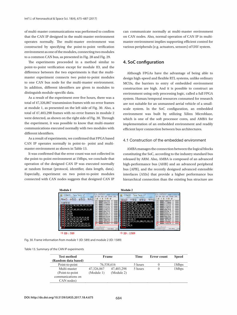
DOI: http://dx.doi.org/10.5139/IJASS.2017.18.4.675 684
Int’l J. of Aeronautical & Space Sci. 18(4), 675–687 (2017)
of multi-master communications was performed to confirm
that the CAN IP designed in the multi-master environment
operates normally. The multi-master environment was
constructed by specifying the point-to-point verification
environment as one of the modules, connecting two modules
to a common CAN bus, as presented in Fig. 28 and Fig. 29.
The experiments proceeded in a method similar to
point-to-point verification except for module ID, and the
difference between the two experiments is that the multi-
master experiment connects two point-to-point modules
to one CAN bus node for the multi-master environment.
In addition, different identifiers are given to modules to
distinguish module-specific data.
As a result of the experiment over five hours, there was a
total of 47,326,867 transmission frames with no error frames
at module 1, as presented on the left side of Fig. 30. Also, a
total of 47,403,298 frames with no error frames in module 2
were detected, as shown on the right side of Fig. 30. Through
the experiment, it was possible to know that multi-master
communications executed normally with two modules with
different identifiers.
As a result of experiments, we confirmed that FPGA based
CAN IP operates normally in point-to- point and multi-
master environment as shown in Table 13.
It was confirmed that the error count was not collected in
the point-to-point environment at 1Mbps, we conclude that
operation of the designed CAN IP was executed normally
at random format (protocol, identifier, data length, data).
Especially, experiment on two point-to-point modules
connected with CAN nodes suggests that designed CAN IP
can communicate normally at multi-master environment
on CAN nodes. Also, normal operation of CAN IP in multi-
master environment implies supporting efficient control for
various peripherals (e.g. actuators, sensors) of UAV system.
4. SoC configuration
Although FPGAs have the advantage of being able to
design high-speed and flexible RTL systems, unlike ordinary
MCUs, the barriers to entry of embedded environment
construction are high. And it is possible to construct an
environment using only processing logic, called a full FPGA
system. Human/temporal resources consumed for research
are not suitable for an unmanned aerial vehicle of a small-
scale system. In the SoC configuration, an embedded
environment was built by utilizing Xilinx Microblaze,
which is one of the soft processor cores, and AMBA for
implementation of an embedded environment and readily
efficient layer connection between bus architectures.
4.1 Construction of the embedded environment
AMBA manages the connection between the logical blocks
constituting the SoC, according to the industry standard bus
released by ARM. Also, AMBA is composed of an advanced
high-performance bus (AHB) and an advanced peripheral
bus (APB), and the recently designed advanced extensible
interfaces (AXIs) that provide a higher performance bus
hierarchical connection than the existing bus structure are
20
Fig. 29. Concept of the multi-master test
The experiments proceeded in a method similar to point-to-point verification except for module ID,
and the difference between the two experiments is that the multi-master experiment connects two
point-to-point modules to one CAN bus node for the multi-master environment. In addition, different
identifiers are given to modules to distinguish module-specific data.
Fig. 30. Frame information from module 1 (ID: 589) and module 2 (ID: 1589)
As a result of the experiment over five hours, there was a total of 47,326,867 transmission frames
with no error frames at module 1, as presented on the left side of Fig. 30. Also, a total of 47,403,298
frames with no error frames in module 2 were detected, as shown on the right side of Fig. 30. Through
the experiment, it was possible to know that multi-master communications executed normally with
two modules with different identifiers.
Fig. 30. Frame information from module 1 (ID: 589) and module 2 (ID: 1589)
Table 13. Summary of the CAN IP experiments
3
Table. 13. Summary of the CAN IP experiments
Test method (Random data based)
Frame Time Error count Speed
Point-to-point 76,538,616 5 hours 0 1Mbps Multi-master
(Point-to-point communications on
CAN nodes)
47,326,867 (Module 1)
47,403,298 (Module 2)
5 hours 0 1Mbps
Table. 14. List of APB IP packed in the FPGA module
APB list IP instance Base address APB_1 PIC 0x79400000 APB_2 Timer 0x70400000 ABP_3 UART 0x70420000 ABP_4 CAN 0x70440000 APB_5 SPI 0x70460000 APB_6 I2C 0x70480000 APB_7 PWM 0x704A0000 APB_8 SDLC 0x704C0000 APB_9 Commutator 0x704E0000
Table. 15. Integrated module SLU specification in a Spartan 6 LX 25
Slice Used Available Utilization REG 4,888 30,064 16 % LUTs 5,875 15,032 39 %
Occupied 2,332 3,758 62 % MUXCYs 816 7,516 10 %
Utilization average 32%
Table. 16. FPGA board specifications
Board specifications FPGA Xilinx Spartan 6 LX 25(100Mhz) Flash Cypress S25FL128SAGNF1001(128MB) Connector PMOD(Module connector x 14) x 8 Emulator JTAG header(Digilent HS3) Others Compile LED/Reset/Flash boot selector
(675~687)2017-156.indd 684 2018-01-05 오후 8:42:18
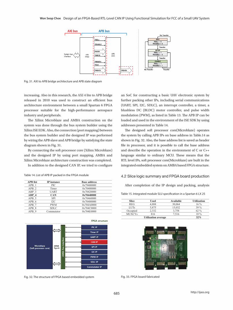
685
Won Seop Choe Design of an FPGA-Based RTL-Level CAN IP Using Functional Simulation for FCC of a Small UAV System
http://ijass.org
increasing. Also in this research, the AXI 4 lite to APB bridge
released in 2010 was used to construct an efficient bus
architecture environment between a small Spartan 6 FPGA
processor suitable for the high-performance aerospace
industry and peripherals.
The Xilinx Microblaze and AMBA construction on the
system was done through the bus system builder using the
Xilinx ISE EDK. Also, the connection (port mapping) between
the bus system builder and the designed IP was performed
by wiring the APB slave and APB bridge by satisfying the state
diagram shown in Fig. 31.
By connecting the soft processor core (Xilinx Microblaze)
and the designed IP by using port mapping, AMBA and
Xilinx Microblaze architecture construction was completed.
In addition to the designed CAN IP, we tried to configure
an SoC for constructing a basic UAV electronic system by
further packing other IPs, including serial communications
(UART, SPI, I2C, SDLC), an interrupt controller, a timer, a
blushless DC (BLDC) motor controller, and pulse width
modulation (PWM), as listed in Table 13. The APB IP can be
loaded and used in the environment of the ISE SDK by using
addresses presented in Table 14.
The designed soft processor core(Microblaze) operates
the system by calling APB IPs on base address in Table.14 as
shown in Fig. 32. Also, the base address list is saved as header
file in processor, and it is possible to call the base address
and describe the operation in the environment of C or C++
language similar to ordinary MCU. These means that the
RTL level IPs, soft processor core(Microblaze) are built in the
integrated embedded system on AMBA based FPGA structure.
4.2 Slice logic summary and FPGA board production
After completion of the IP design and packing, analysis
Table 14. List of APB IP packed in the FPGA module
3
Table. 13. Summary of the CAN IP experiments
Test method (Random data based)
Frame Time Error count Speed
Point-to-point 76,538,616 5 hours 0 1Mbps Multi-master
(Point-to-point communications on
CAN nodes)
47,326,867 (Module 1)
47,403,298 (Module 2)
5 hours 0 1Mbps
Table. 14. List of APB IP packed in the FPGA module
APB list IP instance Base address APB_1 PIC 0x79400000 APB_2 Timer 0x70400000 ABP_3 UART 0x70420000 ABP_4 CAN 0x70440000 APB_5 SPI 0x70460000 APB_6 I2C 0x70480000 APB_7 PWM 0x704A0000 APB_8 SDLC 0x704C0000 APB_9 Commutator 0x704E0000
Table. 15. Integrated module SLU specification in a Spartan 6 LX 25
Slice Used Available Utilization REG 4,888 30,064 16 % LUTs 5,875 15,032 39 %
Occupied 2,332 3,758 62 % MUXCYs 816 7,516 10 %
Utilization average 32%
Table. 16. FPGA board specifications
Board specifications FPGA Xilinx Spartan 6 LX 25(100Mhz) Flash Cypress S25FL128SAGNF1001(128MB) Connector PMOD(Module connector x 14) x 8 Emulator JTAG header(Digilent HS3) Others Compile LED/Reset/Flash boot selector
22
to construct an efficient bus architecture environment between a small Spartan 6 FPGA processor
suitable for the high-performance aerospace industry and peripherals.
The Xilinx Microblaze and AMBA construction on the system was done through the bus system
builder using the Xilinx ISE EDK. Also, the connection (port mapping) between the bus system
builder and the designed IP was performed by wiring the APB slave and APB bridge by satisfying the
state diagram shown in Fig. 31.
Fig. 31. AXI to APB bridge architecture and APB state diagram
By connecting the soft processor core (Xilinx Microblaze) and the designed IP by using port
mapping, AMBA and Xilinx Microblaze architecture construction was completed.
In addition to the designed CAN IP, we tried to configure an SoC for constructing a basic UAV
electronic system by further packing other IPs, including serial communications (UART, SPI, I2C,
SDLC), an interrupt controller, a timer, a blushless DC (BLDC) motor controller, and pulse width
modulation (PWM), as listed in Table 13. The APB IP can be loaded and used in the environment of
the ISE SDK by using addresses presented in Table 14.
Table. 14. List of APB IP packed in the FPGA module
APB list IP instance Base address APB_1 PIC 0x79400000 APB_2 Timer 0x70400000 ABP_3 UART 0x70420000 ABP_4 CAN 0x70440000 APB_5 SPI 0x70460000 APB_6 I2C 0x70480000 APB_7 PWM 0x704A0000 APB_8 SDLC 0x704C0000
Fig. 31. AXI to APB bridge architecture and APB state diagram
23
APB_9 Commutator 0x704E0000
The designed soft processor core(Microblaze) operates the system by calling APB IPs on base
address in Table.14 as shown in Fig. 32. Also, the base address list is saved as header file in processor,
and it is possible to call the base address and describe the operation in the environment of C or C++
language similar to ordinary MCU. These means that the RTL level IPs, soft processor
core(Microblaze) are built in the integrated embedded system on AMBA based FPGA structure.
Fig. 42. The structure of FPGA based embedded system
4.2 Slice logic summary and FPGA board production
After completion of the IP design and packing, analysis of slice logic utilization (SLU) of the
FPGA module designed using the summary report supported by the Xilinx ISE suite was performed,
as shown in Table 15.
Table. 15. Integrated module SLU specification in a Spartan 6 LX 25
Slice Used Available Utilization REG 4,888 30,064 16 % LUTs 5,875 15,032 39 %
Occupied 2,332 3,758 62 % MUXCYs 816 7,516 10 %
Utilization average 32%
It can be seen that the elements shown in Table 15 were not over-mapped and were designed within
the normal range (65~70%). In addition, the remaining slice utilization suggests that the SoC can be
Fig. 32. The structure of FPGA based embedded system
Table 15. Integrated module SLU specification in a Spartan 6 LX 25
3
Table. 13. Summary of the CAN IP experiments
Test method (Random data based)
Frame Time Error count Speed
Point-to-point 76,538,616 5 hours 0 1Mbps Multi-master
(Point-to-point communications on
CAN nodes)
47,326,867 (Module 1)
47,403,298 (Module 2)
5 hours 0 1Mbps
Table. 14. List of APB IP packed in the FPGA module
APB list IP instance Base address APB_1 PIC 0x79400000 APB_2 Timer 0x70400000 ABP_3 UART 0x70420000 ABP_4 CAN 0x70440000 APB_5 SPI 0x70460000 APB_6 I2C 0x70480000 APB_7 PWM 0x704A0000 APB_8 SDLC 0x704C0000 APB_9 Commutator 0x704E0000
Table. 15. Integrated module SLU specification in a Spartan 6 LX 25
Slice Used Available Utilization REG 4,888 30,064 16 % LUTs 5,875 15,032 39 %
Occupied 2,332 3,758 62 % MUXCYs 816 7,516 10 %
Utilization average 32%
Table. 16. FPGA board specifications
Board specifications FPGA Xilinx Spartan 6 LX 25(100Mhz) Flash Cypress S25FL128SAGNF1001(128MB) Connector PMOD(Module connector x 14) x 8 Emulator JTAG header(Digilent HS3) Others Compile LED/Reset/Flash boot selector
24
utilized through communications, driving, and additional system IPs, for UAVs, even in a small
Spartan 6 FPGA model.
Finally, the bit stream file of the logic SoC was extracted, and the FPGA board, like the one in
Fig. 33, was fabricated by referring to the Xilinx printed circuit board user guide for physical
implementation of the SoC [15,16]. The specifications of the designed FPGA board are shown in
Table 16. In addition, construction of the SoC was completed by downloading the bit stream file to
nonvolatile flash memory on the produced FPGA board.
Fig. 33. FPGA board fabricated
Table. 16. FPGA board specifications
Board specifications FPGA Xilinx Spartan 6 LX 25(100Mhz) Flash Cypress S25FL128SAGNF1001(128MB) Connector PMOD(Module connector x 14) x 8 Emulator JTAG header(Digilent HS3) Others Compile LED/Reset/Flash boot selector
5. Conclusion
In this paper, design of an FPGA-based RTL-level CAN IP functional simulation, and configuration
of an SoC were conducted. The CAN protocol configuration was implemented by RTL-level
Hardware Description Language for design of the FPGA vendor–independent IP. In addition, the
flexibility of the FPGA was further enhanced through registers that can be modified by the user.
For logical verification of the designed IP, functional simulation was conducted. In simulation
experiments, functions including error detection and format identification were performed normally.
Also, an AMBA-based soft processor core implantation using the designed IP was suggested for
Fig. 33. FPGA board fabricated
(675~687)2017-156.indd 685 2018-01-05 오후 8:42:19
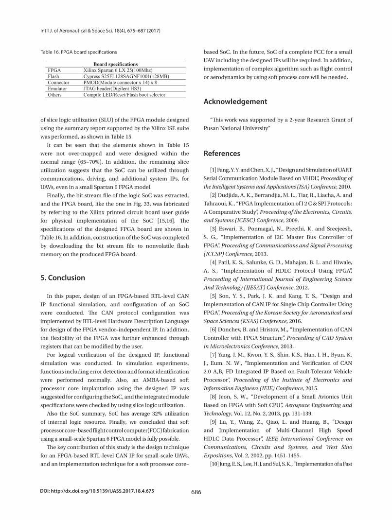
DOI: http://dx.doi.org/10.5139/IJASS.2017.18.4.675 686
Int’l J. of Aeronautical & Space Sci. 18(4), 675–687 (2017)
of slice logic utilization (SLU) of the FPGA module designed
using the summary report supported by the Xilinx ISE suite
was performed, as shown in Table 15.
It can be seen that the elements shown in Table 15
were not over-mapped and were designed within the
normal range (65~70%). In addition, the remaining slice
utilization suggests that the SoC can be utilized through
communications, driving, and additional system IPs, for
UAVs, even in a small Spartan 6 FPGA model.
Finally, the bit stream file of the logic SoC was extracted,
and the FPGA board, like the one in Fig. 33, was fabricated
by referring to the Xilinx printed circuit board user guide
for physical implementation of the SoC [15,16]. The
specifications of the designed FPGA board are shown in
Table 16. In addition, construction of the SoC was completed
by downloading the bit stream file to nonvolatile flash
memory on the produced FPGA board.
5. Conclusion
In this paper, design of an FPGA-based RTL-level CAN
IP functional simulation, and configuration of an SoC
were conducted. The CAN protocol configuration was
implemented by RTL-level Hardware Description Language
for design of the FPGA vendor–independent IP. In addition,
the flexibility of the FPGA was further enhanced through
registers that can be modified by the user.
For logical verification of the designed IP, functional
simulation was conducted. In simulation experiments,
functions including error detection and format identification
were performed normally. Also, an AMBA-based soft
processor core implantation using the designed IP was
suggested for configuring the SoC, and the integrated module
specifications were checked by using slice logic utilization.
Also the SoC summary, SoC has average 32% utilization
of internal logic resource. Finally, we concluded that soft
processor core–based flight control computer(FCC) fabrication
using a small-scale Spartan 6 FPGA model is fully possible.
The key contribution of this study is the design technique
for an FPGA-based RTL-level CAN IP for small-scale UAVs,
and an implementation technique for a soft processor core–
based SoC. In the future, SoC of a complete FCC for a small
UAV including the designed IPs will be required. In addition,
implementation of complex algorithm such as flight control
or aerodynamics by using soft process core will be needed.
Acknowledgement
“This work was supported by a 2-year Research Grant of
Pusan National University”
References
[1] Fang, Y. Y. and Chen, X. J., “Design and Simulation of UART
Serial Communication Module Based on VHDL”, Proceeding of
the Intelligent Systems and Applications (ISA) Conference, 2010.
[2] Oudjida, A. K., Berrandjia, M. L., Tiar, R., Liacha, A. and
Tahraoui, K., “FPGA Implementation of I 2 C & SPI Protocols:
A Comparative Study”, Proceeding of the Electronics, Circuits,
and Systems (ICESC) Conference, 2009.
[3] Eswari, B., Ponmagal, N., Preethi, K. and Sreejeesh,
S. G., “Implementation of I2C Master Bus Controller of
FPGA”, Proceeding of Communications and Signal Processing
(ICCSP) Conference, 2013.
[4] Patil, K. S., Salunke, G. D., Mahajan, B. L. and Hiwale,
A. S., “Implementation of HDLC Protocol Using FPGA”,
Proceeding of International Journal of Engineering Science
And Technology (IJESAT) Conference, 2012.
[5] Son, Y. S., Park, J. K. and Kang, T. S., “Design and
Implementation of CAN IP for Single Chip Controller Using
FPGA”, Proceeding of the Korean Society for Aeronautical and
Space Sciences (KSAS) Conference, 2016.
[6] Donchev, B. and Hristov, M., “Implementation of CAN
Controller with FPGA Structure”, Proceeding of CAD System
in Microelectronics Conference, 2013.
[7] Yang, J. M., Kwon, Y. S., Shin. K.S., Han. J. H., Byun. K.
J., Eum. N. W., “Implementation and Verification of CAN
2.0 A,B, FD Integrated IP Based on Fault-Tolerant Vehicle
Processor”, Proceeding of the Institute of Electronics and
Information Engineers (IEIE) Conference, 2015.
[8] Jeon, S. W., “Development of a Small Avionics Unit
Based on FPGA with Soft CPU”, Aerospace Engineering and
Technology, Vol. 12, No. 2, 2013, pp. 131-139.
[9] Lu, Y., Wang, Z., Qiao, L. and Huang, B., “Design
and Implementation of Multi-Channel High Speed
HDLC Data Processor”, IEEE International Conference on
Communications, Circuits and Systems, and West Sino
Expositions, Vol. 2, 2002, pp. 1451-1455.
[10] Jung, E. S., Lee, H. J. and Sul, S. K., “Implementation of a Fast
Table 16. FPGA board specifications
3
Table. 13. Summary of the CAN IP experiments
Test method (Random data based)
Frame Time Error count Speed
Point-to-point 76,538,616 5 hours 0 1Mbps Multi-master
(Point-to-point communications on
CAN nodes)
47,326,867 (Module 1)
47,403,298 (Module 2)
5 hours 0 1Mbps
Table. 14. List of APB IP packed in the FPGA module
APB list IP instance Base address APB_1 PIC 0x79400000 APB_2 Timer 0x70400000 ABP_3 UART 0x70420000 ABP_4 CAN 0x70440000 APB_5 SPI 0x70460000 APB_6 I2C 0x70480000 APB_7 PWM 0x704A0000 APB_8 SDLC 0x704C0000 APB_9 Commutator 0x704E0000
Table. 15. Integrated module SLU specification in a Spartan 6 LX 25
Slice Used Available Utilization REG 4,888 30,064 16 % LUTs 5,875 15,032 39 %
Occupied 2,332 3,758 62 % MUXCYs 816 7,516 10 %
Utilization average 32%
Table. 16. FPGA board specifications
Board specifications FPGA Xilinx Spartan 6 LX 25(100Mhz) Flash Cypress S25FL128SAGNF1001(128MB) Connector PMOD(Module connector x 14) x 8 Emulator JTAG header(Digilent HS3) Others Compile LED/Reset/Flash boot selector
(675~687)2017-156.indd 686 2018-01-05 오후 8:42:19
687
Won Seop Choe Design of an FPGA-Based RTL-Level CAN IP Using Functional Simulation for FCC of a Small UAV System
http://ijass.org
Current Controller Using FPGA”, The Transactions of the Korean
Institute of Power Electronics, Vol. 12, No. 4, 2007, pp. 339-345.
[11] Oh, K. H., Shim, H. S., Park, D. H. and Ra, S. W., “Design
and Implementation of Data Terminal Controller for UAV
Using FPGA”, Journal of The Korean Society for Aeronautical
and Space Sciences, Vol. 40, No. 5, 2012, pp. 454-460.
[12] Chang, K. C., Digital Design & Modeling with VHDL
and Synthesis, IEEE Computer Society Press, 1996.
[13] Kim, Y. S., Kim, J. H., Han, D. I., Lee, M. H., Park, J.
H. and Lee, D. W., “FPGA Based HW/SW Co-Design for
Vision Based Real-Time Position Measurement of an UAV”,
International Journal of Aeronautical and Space Sciences,
Vol. 17, No. 2, 2016, pp. 232-239.
[14] Abbas, S. H., Lee, J. R. and Kim, Z., “FPGA-Based
Design and Implementation of Data Acquisition and
Real-Time Processing for Laser Ultrasound Propagation”,
International Journal of Aeronautical and Space Sciences,
Vol. 17, No. 4, 2016, pp. 467-475.
[15] Xilinx, “7 Series FPGAs PCB Design Guide(UG483)”,
Xilinx, 2017, pp. 2-76.
[16] Xilinx, “Spartan-6 FPGA Configuration User
Guide(UG380)”, Xilinx, 2009, pp. 2-174.
Appendix
Eight-bit CAN register information by address and functions
5
Appendix A. Eight-bit CAN register information by address and functions
CAN ADD
OPERATING MODE RESET MODE
READ WRITE READ WRITE
0 Mode Mode Mode Mode
1 (00H) Command (00H) Command
2 Status - Status -
3 Interrupt - Interrupt -
4 Interrupt enable Interrupt enable Interrupt enable Interrupt enable
6 Bus timing 0 - Bus timing 0 Bus timing 0
7 Bus timing 1 - Bus timing 1 Bus timing 1
11 Arbitration lost capture - Arbitration lost capture -
12 Error code capture - Error code capture -
14 RX error counter - RX error counter RX error counter
15 TX error counter - TX error counter TX error counter
16 RX frame information SFF
RX frame information EFF
TX frame information SFF
TX frame information EFF
Acceptance Code 1 Acceptance Code 1
17 RX identifier 1
RX identifier 1
TX identifier 1
TX identifier 1 Acceptance Code 2 Acceptance Code 2
18 RX identifier 2
RX identifier 2
TX identifier 2
TX identifier 2 Acceptance Code 3 Acceptance Code 3
19 RX data 1 RX identifier 3 TX data 1 TX
identifier 3 Acceptance Code 4 Acceptance Code 4
20 RX data 2 RX identifier 4 TX data 2 TX
identifier 4 Acceptance Mask 1 Acceptance Mask 1
21 RX data 3 RX data 1 TX data 3 TX data 1 Acceptance Mask 2 Acceptance Mask 2
22 RX data 4 RX data 2 TX data 4 TX data 2 Acceptance Mask 3 Acceptance Mask 3
23 RX data 5 RX data 3 TX data 5 TX data 3 Acceptance Mask 4 Acceptance Mask 4
24 RX data 6 RX data 4 TX data 6 TX data 4 Reserved -
25 RX data 7 RX data 5 TX data 7 TX data 5 Reserved -
26 RX data 8 RX data 6 TX data 8 TX data 6 Reserved -
27 - RX data 7 - TX data 7 Reserved
28 - RX data 8 - TX data 8 Reserved
29 RX message counter - RX message counter -
31 Clock divider Clock divider Clock divider Clock divider
(675~687)2017-156.indd 687 2018-01-05 오후 8:42:19
![Embedded System Design using FPGA - Indico [Home]indico.ictp.it/event/a12223/session/78/contribution/52/material/0/... · Logic circuit design ... Synthesizable RTL, Gate level, IPs,](https://cdn.vdocument.in/doc/165x107/5ab10ad67f8b9ac3348be31e/embedded-system-design-using-fpga-indico-home-circuit-design-synthesizable.jpg)


