
Design of Z-Source Inverter for Electric Bikes
Wencong Zhang
Electrical Engineering and Computer SciencesUniversity of California at Berkeley
Technical Report No. UCB/EECS-2017-53http://www2.eecs.berkeley.edu/Pubs/TechRpts/2017/EECS-2017-53.html
May 11, 2017

Copyright © 2017, by the author(s).All rights reserved.
Permission to make digital or hard copies of all or part of this work forpersonal or classroom use is granted without fee provided that copies arenot made or distributed for profit or commercial advantage and that copiesbear this notice and the full citation on the first page. To copy otherwise, torepublish, to post on servers or to redistribute to lists, requires priorspecific permission.
Acknowledgement
I would like to thank my advisor, Professor Seth Sanders, for his insightfulguidance and support on the project. I would also like to acknowledgeProfessor Jose Antonio Cobos Marquez for his comments and contribution.Finally, I would like to thank my fiancée and family for their support andfaith in me.

Design of Z-Source Inverter for Electric Bikes
by Wencong Zhang
Research Project
Submitted to the Department of Electrical Engineering and Computer Sciences, University of California at Berkeley, in partial satisfaction of the requirements for the degree of Master of Science, Plan II. Approval for the Report and Comprehensive Examination:
Committee:
Professor Seth Sanders Research Advisor
(Date)
* * * * * * *
Professor Jose Antonio Cobos Marquez Second Reader
(Date)

Acknowledgements
I would like to thank my advisor, Professor Seth Sanders, for his insightful guidance and
support on the project. I would also like to acknowledge Professor Jose Antonio Cobos Marquez
for his comments and contribution. Finally, I would like to thank my fiancée and family for their
support and faith in me.

Abstract
This technical report presents the design of a Z-source inverter for an electric bike
controller. The objective of this work is to evaluate the potential of using this non-standard
inverter topology for a medium power (250W - 3kW) motor drive application. The Z-source
inverter is able to use the shoot-through state to boost the dc bus voltage, which enables a
permanent magnet motor to achieve a higher top speed. In addition to a concise review of
relevant work done on this topic, this report also presents an original analysis on the switching
behavior of the Z-source inverter and proposes the minimum switching space vector modulation
control strategy. The design of a 1.5kW Z-source inverter prototype is detailed and the
advantages of the proposed control strategy are verified experimentally.

Contents
1. Introduction 2. Z-Source Inverter Overview
2.1 Topology and Principles of Operation
2.2 Z-source Inverter Modulation Strategies
2.3 Z-Source Inverter Switching Analysis
2.4 Impedance Network Passives Requirement Analysis
3. Z-Source Inverter Design and Implementation
3.1 Circuit Design and Layout
3.2 Minimum Switching Space Vector Modulation
4. Experimental Results
4.1 Z-Source Inverter Modes of Operation
4.2 Z-Source Inverter Loss Analysis
4.3 Minimum Switching Space Vector Modulation Control Results
5. Conclusion
Appendices:
1 Differential Power Analysis for ZSI
2 Minimum Switching SVM Algorithm
3 Differential Power Comparison Between Control Methods

Introduction
Power inverters are a class of circuits that convert DC power to AC power and they are
the fundamental building block of any electric variable speed drives. With the growing
electrification of transport, there is a need to design inverters suitable for a range of drive
applications. This report focuses on the inverter design for a low to medium power (250W -
3kW) drive application such as an electric bicycle or an electric moped.
Any battery-powered electric drive system consists of three basic building blocks:
batteries, power inverters and electric machines. In the case of an electric bike, sealed lead-acid
(SLA) batteries or Li-ion batteries (Fig.1) are the most commonly used. Asia accounts for 90%
of the global market for electric bikes and most e-bikes sold in Asia use SLA batteries due to
their relatively lower cost. A typical battery arrangement is to put three to six 12V SLA battery
packs in series to provide 36 to 72V source voltage. Li-ion batteries are used on high-
performance e-bikes for their much superior energy density. Typically, 18650 Li-ion cells with
nominal voltage 3.7V are configured in a series-parallel connection to provide the desired
voltage and maximum current output capability; the pack voltage is commonly configured to be
from 24V to 72V.
Figure 1(a): 12V SLA Battery
Figure 1(b): E-bike Li-ion Battery Pack

The electric machines employed in these electric drive systems are almost exclusively
surface permanent magnet synchronous machines (SPM) because of their simplicity and high
torque density (Fig. 2a). Gears may be used in motors with small form factors to trade speed for
torque (Fig. 2b). The torque output of a SPM is proportional to its current and its back-EMF is
proportional to its speed. Therefore, if a voltage source inverter is used, which can only step
down the input voltage, the voltage of the battery pack determines the top speed or no-load speed
of a SPM. In addition, as the motor approaches its top speed, its torque and power output drop
sharply because the battery pack does not have enough voltage to push high current into the fast-
spinning motor. For induction machines that are sometimes used on electric vehicles (EVs), field
weakening can be used to extend the speed of the machine beyond its base speed. This is
achieved by reducing its magnetizing current hence the air gap flux. This technique is inefficient
and even impractical with SPMs because the windings in an SPM typically have low inductance,
which means that it would require a significant amount of current to counteract the magnetic
field provided by the permanent magnets. The heat generated from this large amount of current
not only reduces the efficiency of the drive, but also runs the risk of overheating under
continuous operation.
Figure 2(a): E-bike SPM
Figure 2(b): Planetary Gears in an E-bike Hub Motor
To increase the top speed of an SPM, the most direct approach is to have an inverter that
is able to boost the battery voltage. A boost converter front-end is well suited for this purpose
although the costs of extra circuitry and control complexity have prohibited the
commercialization of such two-staged approach for low to medium power drive systems (Fig. 3).
A novel single-stage topology that has received a lot of attention recently is the Z-source

inverter, which utilizes the traditionally forbidden shoot-through states to boost the voltage. (Fig.
4) [1]. Having the voltage boost functionality in an inverter does not only allow the motor to go
faster, but also allows the motor to maintain constant speed under battery voltage fluctuations.
Figure 3: 2-Stage Boosted Inverter Topology
Figure 4: Z-Source Inverter Topology
The concept of a Z-source inverter was first proposed in 2002 by Prof. F.Z.Peng [1].
Since then, Z-source-related research has grown rapidly: an array of Z-source inverter topologies
and control strategies has been proposed to improve on the original concept. This report
discusses the design of a 1.5kW Z-source inverter for an e-bike application and presents a new
control strategy that reduces switching loss and the average stresses on the switching devices and
passives compared to the popular constant boost control [2].

Z-Source Inverter Overview
Topology and Principles of Operation
The Z-source inverter topology, shown in Fig.4, has a unique impedance network front-
end consisting of two inductors and two capacitors. Compared to a voltage-source inverter that
can only operate in 6 actives states and 2 zero states, the Z-source inverter can also operate in the
shoot-through states where the upper and lower switches in one or more phase legs are gated on
simultaneously. Since shoot-through events no longer result in inverter failures, the Z-source
inverter is more robust against EMI and parasitic turn-on of devices. Illustrated in Fig.5 are the
equivalent circuits of the shoot-through states and non shoot-through states of the Z-source
inverter.
Figure 5(a): ZSI in Shoot-through State
Figure 5(b): ZSI in non Shoot-through State
In the following description of the circuit operation, we assume that the capacitors in the
impedance network (C1 and C2) are identical. We also make this assumption for the inductors L1
and L2. Then, based on the symmetry of the circuit, capacitor voltages and inductor currents are
typically observed to be the same in practice. The capacitors in the impedance network (C1 and
C2) are initially charged to the input voltage Vin. During the shoot-through state, the source diode
D1 is reverse biased and it blocks a voltage 2Vcap - Vin. Therefore, the input is disconnected from
the rest of the circuit. Due to the short circuit in one or more phase legs, the voltage across each
inductor in the impedance network (L1 and L2) is Vcap; energy is transferred from C1 to L1 and C2
to L2. In the non shoot-through state, the diode D1 is forward biased and the inverter bus voltage
is 2Vcap - Vin; energy is transferred from L1 to C2 and L2 to C1.

The detailed derivation of the steady state voltages has been presented in [1] and this
report presents some key equations relevant to inverter operation and control design. In the
following equations, d represents the shoot-through duty cycle, M is the modulation depth of the
inverter, B is the boost factor from input voltage to inverter bus voltage, < > means taking the
periodic average of the value inside the bracket, VAC is the output peak AC voltage without using
overmodulation and Vbus_nst is the Vbus voltage during non shoot-through state.
𝑉!"# = !!!!!!!
𝑉!" (1)
𝑉!"#_!"# = !!!!!
𝑉!" (2)
𝐼! = 𝐼!" (3)
𝑉!" = 𝑀×𝐵× !!"!
(4)
It is worth mentioning that there are variant Z-source topologies based on the original Z-
source topology presented above. The two most notable variant topologies are the quasi Z-source
inverter and the trans Z-source inverter (Fig. 6). The quasi Z-source inverter has the advantage of
continuous input current and easier layout design [3]. The trans Z-source inverter uses coupled
magnetics to achieve higher voltage gain [3].
Figure 6(a): Quasi ZSI
Figure 6(b): Trans ZSI

Z-source Inverter Modulation Strategies
Reference [4] presents a comprehensive review of different Z-source inverter modulation
strategies. This report focuses on the modulation techniques for three phase (2 Level) Z-source
inverters because they are commonly used in motor drive applications. These proposed strategies
could be broadly categorized as sine PWM (SPWM) and space vector PWM (SVPWM). These
strategies aim to achieve a wide range of modulation, less commutation per switching cycle,
lower device stress and smaller size requirements for passives. Simple control [1], maximum
boost control [5] and maximum constant boost control [2] are widely cited SPWM control
strategies. Since space-vector modulation is a more natural choice for motor drive applications
with the advantage of generating higher voltages with lower THD, this report discusses and
compares the SVPWM ideas. In succinct terms, simple control and constant boost control use
constant modulation depth and constant boost factor. Maximum boost control uses constant
modulation depth and time-varying boost factor.
Unlike a 2-stage boosted inverter topology where the voltage boost is independent of the
modulation depth of the inverter, the Z-source inverter has a fundamental trade-off between
shoot-through states and active states. Therefore, the Z-source inverter is intrinsically inferior in
terms of bus utilization. Simple control presented in [1] has the advantage of implementation
simplicity but does not utilize the inverter bus voltage efficiently. Therefore, the device voltage
stress is high, as an unnecessarily large boost is required to achieve a certain AC output.
Maximum boost control, presented in [2], has the most efficient bus utilization since it converts
all traditional zero states into shoot-through states. However, due to the non-constant shoot-
through duty cycle, large passives are required to suppress the low frequency (6 times the output
frequency) voltage ripple on the inverter bus. Maximum constant boost control with 3rd
harmonic injection proposed in [3] achieves constant shoot-through duty cycle by not converting
all potential zero states. Shown in Fig.7 is the shoot-through duty cycle comparison in an output
period between the two schemes.

Figure 7: Shoot-through Duty Cycle Comparison
The two schemes can also be visualized on a space vector diagram. Shown in Fig.8a is
the maximum boost control. The yellow region represents the time allocated to traditional zero
states that can be converted to shoot-through states. If a constant modulation depth is used, there
is more time for shoot-through states near the vertices of the hexagon. In Fig.8b, the yellow
region representing the shoot-through states has pulled back from the vertices and the green
region represents the unconverted zero states. Under this modulation, the size requirement of the
passives is significantly reduced but it incurs higher voltage stress on the devices compared to
maximum boost control.
Figure 8(a): Maximum Boost Control
Figure 8(b): Maximum Constant Boost Control

Since the shoot-through states can be accessed in the Z-source inverter, the set of possible
gating patterns is larger than that of a voltage source inverter. This freedom to access the shoot-
through states gives rise to new opportunities in designing innovative modulation strategies. The
design of switching patterns is guided by the tradeoff between the size of the passives and
switching loss. In order to minimize the size requirement of the passives in the impedance
network, we want to insert as many shoot through states as possible. However, to keep switching
loss low, we must also minimize the frequency of switching actions. Fig. 9 shows a symmetric
space vector switching pattern where 6 shoot-through events are distributed in a switching
period. This gives us the highest number of shoot-through events in a period without having
more switching events than the traditional symmetric space vector modulation. If we convert all
the zero states, both (000) and (111), into shoot-through states, then two gate signals (A+ and C-
in the example) will be held high throughout the switching period, thus reducing the switching
loss by 1/3 in the converter. This control strategy will be explained in detail in section 4.3.
Figure 9: Modified Symmetric SVM for ZSI

Z-Source Inverter Switching Analysis
The unique topology of the Z-source inverters (ZSI) has attracted much attention from
researchers but the relatively more difficult layout of the ZSI has prohibited its adoption in
industry [3]. For example, significant voltage spikes during switching is a known issue in ZSI.
Regrettably, the analysis of the switching dynamics in ZSI has been largely ignored in literature.
This section aims to provide an original analysis of the switching behaviors of ZSI and
recommend layout and control guidelines to mitigate voltage spikes in ZSI design.
In order to remedy the voltage spikes, the current commutation during switching and the
critical parasitic inductance need to be identified. The analysis of voltage source inverter
commutation is reviewed and extended to the ZSI.
Shown in Fig.10a is a single-phase voltage source inverter. The output is modeled as a
constant current source with amplitude Iout. The yellow loop is where the commutation current
flows and where the parasitic inductance causes ringing at the switching node. The magnitude of
the ringing depends on the parasitic inductance, the magnitude of the commutation current and
the device output capacitance, assuming the gate turn-on/turn-off time has been fixed. In this
case, the magnitude of the commutation current is equal to the absolute value of the output
current; the direction of the output current does not affect the magnitude of the ringing.

Figure 10(a): High Frequency Loop in Voltage
Source Inverter
Figure 10(b): High Frequency Loop in ZSI
A single-phase ZSI is redrawn in Fig.10b. The inductors in the impedance network are
assumed to be large so that current sources of magnitude IL are used to replace them. When the
upper and lower switches are operated without shoot-through, the diode is on. Comparing Fig.9b
with Fig.9a, it is obvious that the commutation current loop is the shaded yellow region and the
magnitude of commutation current is again equal to the absolute value of the output current. The
analysis for state transitions involving the shoot-through state is subtler. We first assume that the
lower switch is on and the upper switch is turned on and off to enter and exit the shoot-through
state. This is shown in Fig.11a. When the top switch is off, the current flowing in it is 0. When
the switch is gated on, the diode is turned off and the current flowing is 2IL. The commutation
current loop is still the yellow region but the magnitude of the current is 2IL. Next we consider
the case where the upper switch is on and the lower switch is turned on and off to enter and exit
the shoot-through state. This is shown in Fig.11b. When the lower switch is gated on, the current
flowing through it jumps from 0 to 2IL - Iout. Therefore, the commutation current loop is still the
yellow region but the magnitude of the current is 2IL - Iout. It is interesting to note that the
direction of the output current matters here; the worst-case commutation current has a magnitude
of 2IL + |Iout| when Iout flows into the switching node.

Figure 11(a): Shoot-through via Upper Switch
Figure 11(b): Shoot-through via Lower Switch
We can extend this analysis to a three-phase ZSI, which is shown in Fig.12. The currents
flowing in the inverter link marked in red are 0, Iout and 2IL in zero, active and shoot-through
states respectively. The worst-case commutation current depends on the direction of Iout. Under
the assumption of unity power factor, Iout is non-negative. As power factor decreases, worst-case
Iout also becomes more negative, resulting in higher commutation current.
Figure 12: High Frequency Loop in ZSI
Impedance Network Passives Requirement Analysis
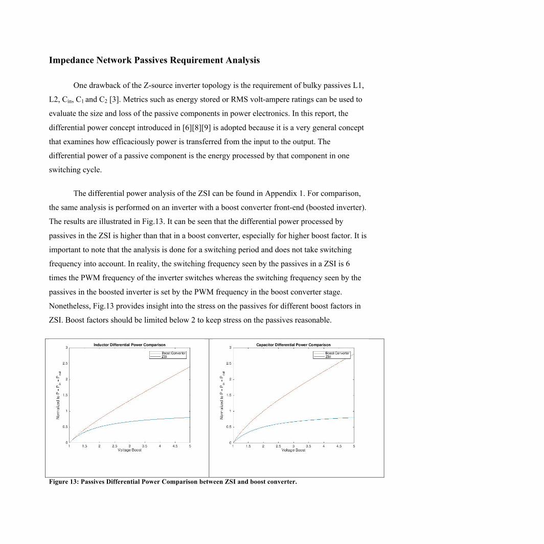
One drawback of the Z-source inverter topology is the requirement of bulky passives L1,
L2, Cin, C1 and C2 [3]. Metrics such as energy stored or RMS volt-ampere ratings can be used to
evaluate the size and loss of the passive components in power electronics. In this report, the
differential power concept introduced in [6][8][9] is adopted because it is a very general concept
that examines how efficaciously power is transferred from the input to the output. The
differential power of a passive component is the energy processed by that component in one
switching cycle.
The differential power analysis of the ZSI can be found in Appendix 1. For comparison,
the same analysis is performed on an inverter with a boost converter front-end (boosted inverter).
The results are illustrated in Fig.13. It can be seen that the differential power processed by
passives in the ZSI is higher than that in a boost converter, especially for higher boost factor. It is
important to note that the analysis is done for a switching period and does not take switching
frequency into account. In reality, the switching frequency seen by the passives in a ZSI is 6
times the PWM frequency of the inverter switches whereas the switching frequency seen by the
passives in the boosted inverter is set by the PWM frequency in the boost converter stage.
Nonetheless, Fig.13 provides insight into the stress on the passives for different boost factors in
ZSI. Boost factors should be limited below 2 to keep stress on the passives reasonable.
Figure 13: Passives Differential Power Comparison between ZSI and boost converter.

Z-Source Inverter Design and Implementation
Circuit Design and Layout
The specifications of the ZSI prototype are listed in Table 1. The selection of passives
and switching devices are presented in Table 2.
Input Voltage 24V - 48V
Max Power 1.5kW
Max Boost Factor 2
Voltage Ripple of Vbus 3%
Current Ripple of Inductors 20%
Switching Frequency 20kHz
Efficiency >95% for most operating points
Table 1: E-bike ZSI Specifications
Components Part/Value Features
Inverter Switches IRFB4110 Vdss = 100V, Id = 120A, Rds(on) =
3.7mOhm
Source Diode D1 APT60S20 200V 75A Schottky with fast recovery
Inductors L1, L2 L_tot = 12uH Custom Coupled Inductor Design
Capacitors Cin, C1, C2 40uF Paktron Film Capacitor with low ESR/ESL
Gate Drive IC UCC27211
Rg 22 Ohm Turn-on time constant = 220ns
Rt, Ct 100 Ohm, 1nF Turn-off time constant = 100ns
Table 2: ZSI Component Selection
The inductor design deserves some discussion. The two inductors L1 and L2 are wound in
a bifilar fashion on the same toroidal core to achieve tight coupling. Since the current flowing
through the two inductors are identical, the coupled inductor design doubles the inductance of
each winding [7]. Therefore, the total number of turns required to build the coupled inductor is
half of that of two separate inductors. This design is critical to reducing the size of the inductors
in a ZSI.
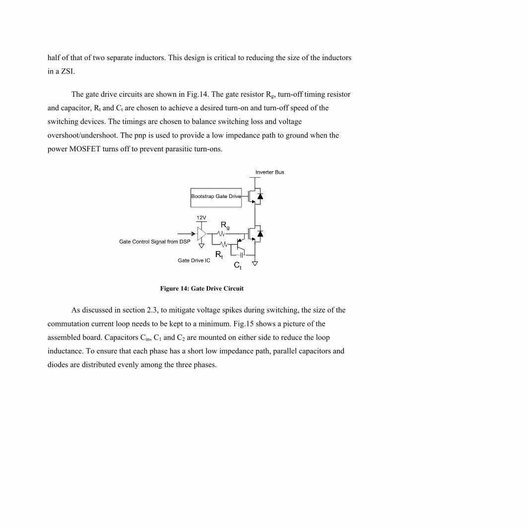
The gate drive circuits are shown in Fig.14. The gate resistor Rg, turn-off timing resistor
and capacitor, Rt and Ct are chosen to achieve a desired turn-on and turn-off speed of the
switching devices. The timings are chosen to balance switching loss and voltage
overshoot/undershoot. The pnp is used to provide a low impedance path to ground when the
power MOSFET turns off to prevent parasitic turn-ons.
Figure 14: Gate Drive Circuit
As discussed in section 2.3, to mitigate voltage spikes during switching, the size of the
commutation current loop needs to be kept to a minimum. Fig.15 shows a picture of the
assembled board. Capacitors Cin, C1 and C2 are mounted on either side to reduce the loop
inductance. To ensure that each phase has a short low impedance path, parallel capacitors and
diodes are distributed evenly among the three phases.
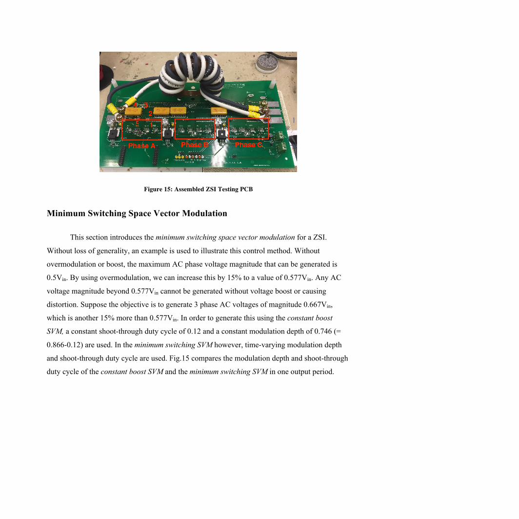
Figure 15: Assembled ZSI Testing PCB
Minimum Switching Space Vector Modulation
This section introduces the minimum switching space vector modulation for a ZSI.
Without loss of generality, an example is used to illustrate this control method. Without
overmodulation or boost, the maximum AC phase voltage magnitude that can be generated is
0.5Vin. By using overmodulation, we can increase this by 15% to a value of 0.577Vin. Any AC
voltage magnitude beyond 0.577Vin cannot be generated without voltage boost or causing
distortion. Suppose the objective is to generate 3 phase AC voltages of magnitude 0.667Vin,
which is another 15% more than 0.577Vin. In order to generate this using the constant boost
SVM, a constant shoot-through duty cycle of 0.12 and a constant modulation depth of 0.746 (=
0.866-0.12) are used. In the minimum switching SVM however, time-varying modulation depth
and shoot-through duty cycle are used. Fig.15 compares the modulation depth and shoot-through
duty cycle of the constant boost SVM and the minimum switching SVM in one output period.

Figure 15: Shoot-through Duty Cycle and Modulation Depth Comparison
Again, these two control methods can be illustrated on a space vector diagrams. In
Fig.16a, constant boost control with a constant shoot-through duty cycle of 0.12 is shown. The
blue traces show the modulation depth trajectory, which is a circle with constant radius. In the
minimum switching space vector modulation shown in Fig.16b, instead of leaving the traditional
zero states near the vertices unconverted, the algorithm utilizes them as active states. To generate
sinusoidal output, we use time-varying boost factor to compensate for the time-varying
modulation depth. The algorithm is detailed in Appendix 2.

Figure 16(a): Constant Boost SVM Example
Figure 16(b): Minimum Switching SVM Example
The minimum switching space vector modulation is superior to the constant boost control
because of the elimination of the traditional zero states, which can be interpreted as the converter
idle state. For α = 30 + 60n degrees where n is an integer from 0 to 5, the modulation depth and
shoot-through duty cycle for the two control schemes are exactly the same. This is because
constant boost control already utilizes all zero states at those angles. These are also the angles at
which the most amount of boosting is required. Therefore, the two control methods have the
same worst-case differential power. However, as the minimum switching SVM uses less boosting
at all other angles, it places less average stress on the devices and passives. To have a more
quantitative comparison, we compare the converter best-case differential power and the average
differential power over one output period in Appendix 3. The results are summarized in Table 3.
Worst Case
(α = 30 + 60n)
Best Case
(α = 60n)
Average over
one output
period
Constant Boost SVM 0.6758 0.6758 0.6638
Min Switching SVM 0.6758 0 0.4526
Table 3: Normalized Converter Differential Power Comparison
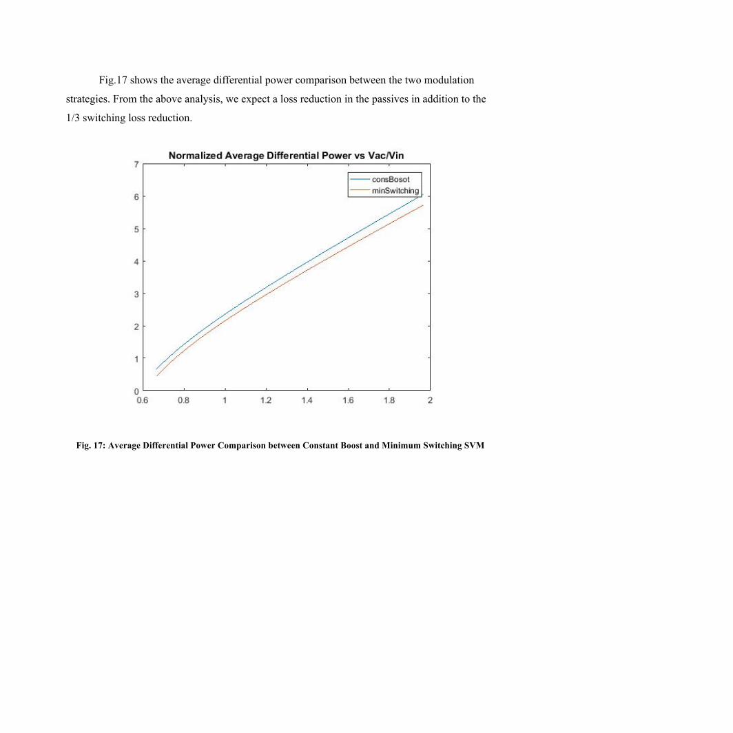
Fig.17 shows the average differential power comparison between the two modulation
strategies. From the above analysis, we expect a loss reduction in the passives in addition to the
1/3 switching loss reduction.
Fig. 17: Average Differential Power Comparison between Constant Boost and Minimum Switching SVM

Experimental Results
Z-Source Inverter Modes of Operation
A 1.5kW Z-source inverter with specifications listed in Table 1 has been designed, built
and tested. During the first phase of testing, the constant boost control is used to evaluate the
performance of the ZSI. Next, the proposed minimum switching SVM is used to demonstrate its
operation and advantages over the constant boost control.
A ZSI has three main modes of operations: self-boost (DCM) mode, no-boost mode and
boost mode. The self-boost mode or DCM occurs under light load conditions even without
intentional insertion of shoot-through states. The boost occurs with the turn-on of body diodes of
the MOSFETs in a phase leg when the inductor (L1 and L2) currents drop below the output
current due to ripple in each PWM period. This scenario is illustrated in Fig.18 and waveforms
showing the self-boost events are in Fig.19. As long as the maximum boosted voltage does not
exceed the voltage rating of the switching devices, this self-boost mode does not present
significant challenges to the design. In fact, this mode is ideal for high-speed coasting on an e-
bike with direct drive permanent magnet motors where the back-EMF of the motor exceeds the
battery voltage.
Figure 18: Self Boost Mode Equivalent Circuit

Figure 19: Self-Boost Mode Waveforms. The time scale is 5us/div. The scales for the yellow, green, red and blue waveforms are 50V/div, 20V/div, 10V/div and 10V/div respectively. There is no shoot-through since the two gate signals (red and blue) are never both high. However, the inverter link voltage goes down to zero in the parasitic boost mode regions, suggesting the output has been shorted by the turn-on of the body diodes in all phase legs. The oscillations in the inverter link voltage (yellow) and switching node voltage (green) are the classical DCM behaviors.
The no-boost mode is used when the output voltage can be generated without the need of
voltage boost. The control and circuit behavior in this mode is identical to those of a voltage
source inverter except the dead time can be set to zero since shoot-through no longer presents a
reliability issue. Operation in this state is the most efficient since the additional losses associated
with the use of shoot-through states are not incurred. However, due to the parasitic inductance of
the high frequency loop, the voltage overshoot on MOSFET turn-off is significant. Fig.20
illustrates the waveforms in this mode of operation.

Figure 20: no-boost mode waveform. The time scale is 10us/div and vertical scales for the waveforms are identical with those in Fig.19. Due to the absence of shoot-through states, the inverter link voltage never goes to zero. The voltage overshoot on MOSFET turn-off is significant.
The boost mode is used to enable generation of even larger voltage output. Operation in
the boost mode is slightly more inefficient compared to the no-boost mode. This is primarily due
to the higher MOSFET conduction loss during the shoot-through states where current of
magnitude 2IL flows through both MOSFETs in a phase leg. There is also more Coss loss: upon
entering the shoot-through state where one phase leg is shorted, the output capacitances of all the
MOSFETs are discharged. Upon transitioning into a non shoot-through state, the Coss of one
MOSFET per phase leg needs to be charged up to a voltage equal to the inverter link voltage.
The Coss loss in the boost mode is approximately 6 times that in the no-boost mode because there
are 6 shoot-through events in a PWM period. However, this loss is very small, less than 1% of
total system loss in the boost mode. The advantage of this operation is that the 3 parallel Coss act
as a snubber capacitance and reduce voltage overshoot on MOSFET turn-off. Fig.21 illustrates
the waveforms in the boost mode.

Figure 21: boost mode waveform. The time scale is 5us/div and vertical scales for the waveforms are identical with those in Fig.19 and Fig.20. Shoot-through occurs when both the high gate signal and the low gate signal are high, where the inverter link voltage and phase voltage go to zero. The inverter link voltage is boosted to around 52V, which is 1.45 times the 36V input voltage. The voltage overshoot on MOSFET turn-off is significantly reduced.
Efficiency and voltage overshoot measurements are carried out on the ZSI prototype.
Table 4 summarizes the testing conditions. The ZSI operates in self-boost mode (DCM) for
output phase current below 12Arms. Then as the modulation depth is increased gradually to 75%
without using shoot-through, the ZSI operates in the no-boost mode for output phase current
between 12Arms to 16Arms. Next, the shoot-through duty cycle is increased gradually from 0%
to 25%; at 25% shoot-through duty cycle, the ZSI achieves the max boost factor of 2. Fig.22
shows the efficiency plot versus output currents. Fig.23 shows the overshoot voltage versus
output currents.
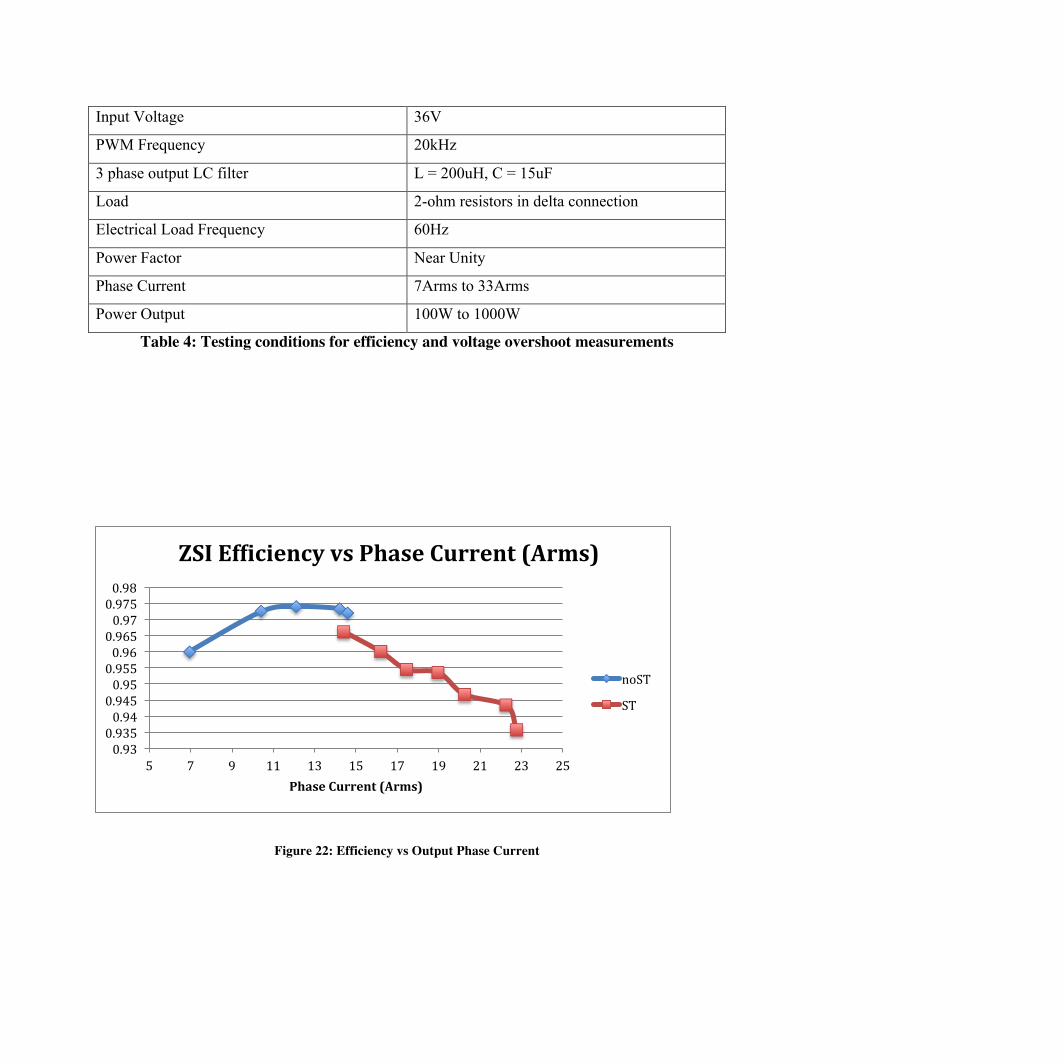
Input Voltage 36V
PWM Frequency 20kHz
3 phase output LC filter L = 200uH, C = 15uF
Load 2-ohm resistors in delta connection
Electrical Load Frequency 60Hz
Power Factor Near Unity
Phase Current 7Arms to 33Arms
Power Output 100W to 1000W
Table 4: Testing conditions for efficiency and voltage overshoot measurements
Figure 22: Efficiency vs Output Phase Current
0.930.9350.940.9450.950.9550.960.9650.970.9750.98
5 7 9 11 13 15 17 19 21 23 25PhaseCurrent(Arms)
ZSIEf5iciencyvsPhaseCurrent(Arms)
noST
ST

Figure 23: Voltage Overshoot vs Phase Current in Different Modes
0
10
20
30
40
50
60
5 10 15 20 25
Overshoot(V)
OutputPhaseCurrent(Arms)
VoltageOvershoot(V)vsPhaseCurrent(Arms)
Self-Boost
No-Boost
Boost

Z-Source Inverter Loss Analysis
The inverter achieves over 95% efficiency for most of its operating points. This section
presents the loss breakdown and evaluates potential circuit or control modifications that can
further improve the efficiency of the converter. Fig. 24 shows the loss breakdown analysis in a
pie chart. The test conditions are the same as listed in Table 4 and the output phase current is
16.5 Arms, resulting in an output power of 550W.
Figure 24: Loss Breakdown Analysis
Losses in the inductor and semiconductor devices account for most of the loss in the
system. Thermal measurements on the heatsinks attached to the MOSFETs and diodes have been
carried out to validate the analysis on the semiconductor losses. The MOSFET switching losses
mainly stem from the overlap of voltage and current during device turn-on/turn-off. Due to the
voltage overshoots and undershoots caused by the parasitic inductance, turn-on and turn-off
times are intentionally slowed down to reduce them at the expense of higher switching loss. To
further improve the efficiency of the converter, one practical approach is to install MOSFETs in

parallel with the source schottky diode D1 to reduce diode conduction losses. Furthermore, the
minimum switching space vector modulation could be used to reduce switching losses.
Minimum Switching Space Vector Modulation Results
This section presents the comparison between the minimum switching SVM and the
constant boost SVM. The two schemes were run to generate an AC voltage of magnitude
0.667Vin at 60Hz from 36V power supply. Due to the voltage drop across the cable between the
power supply and the ZSI prototype, the input voltage is effectively 32V. Shown in Fig.25 is the
output line-to-line voltage waveform generated by the constant boost SVM, which serves as a
benchmark. This waveform is collected after the output LC filter. Shown in Fig.26 is the output
line-to-line voltage waveform generated by the minimum switching SVM. The almost identical
waveforms indicate that the minimum switching SVM, which uses time-varying modulation depth
and shoot-through duty cycle, is able to achieve the same output as the popular constant boost
SVM.
Figure 25: Line-to-line voltage output generated by the constant boost SVM. The time scale is 5ms/div and vertical
scale is 10V/div.
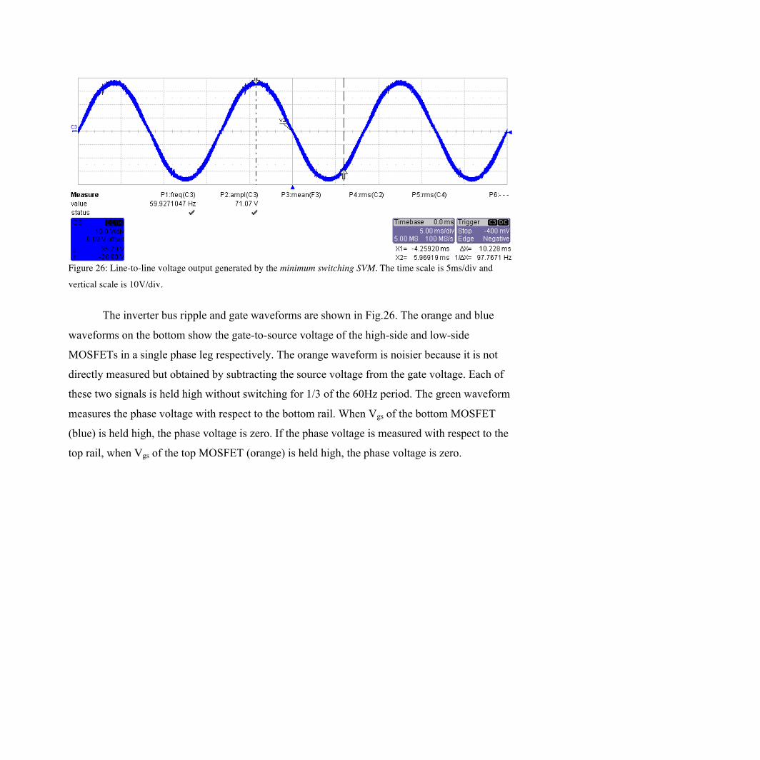
Figure 26: Line-to-line voltage output generated by the minimum switching SVM. The time scale is 5ms/div and
vertical scale is 10V/div.
The inverter bus ripple and gate waveforms are shown in Fig.26. The orange and blue
waveforms on the bottom show the gate-to-source voltage of the high-side and low-side
MOSFETs in a single phase leg respectively. The orange waveform is noisier because it is not
directly measured but obtained by subtracting the source voltage from the gate voltage. Each of
these two signals is held high without switching for 1/3 of the 60Hz period. The green waveform
measures the phase voltage with respect to the bottom rail. When Vgs of the bottom MOSFET
(blue) is held high, the phase voltage is zero. If the phase voltage is measured with respect to the
top rail, when Vgs of the top MOSFET (orange) is held high, the phase voltage is zero.
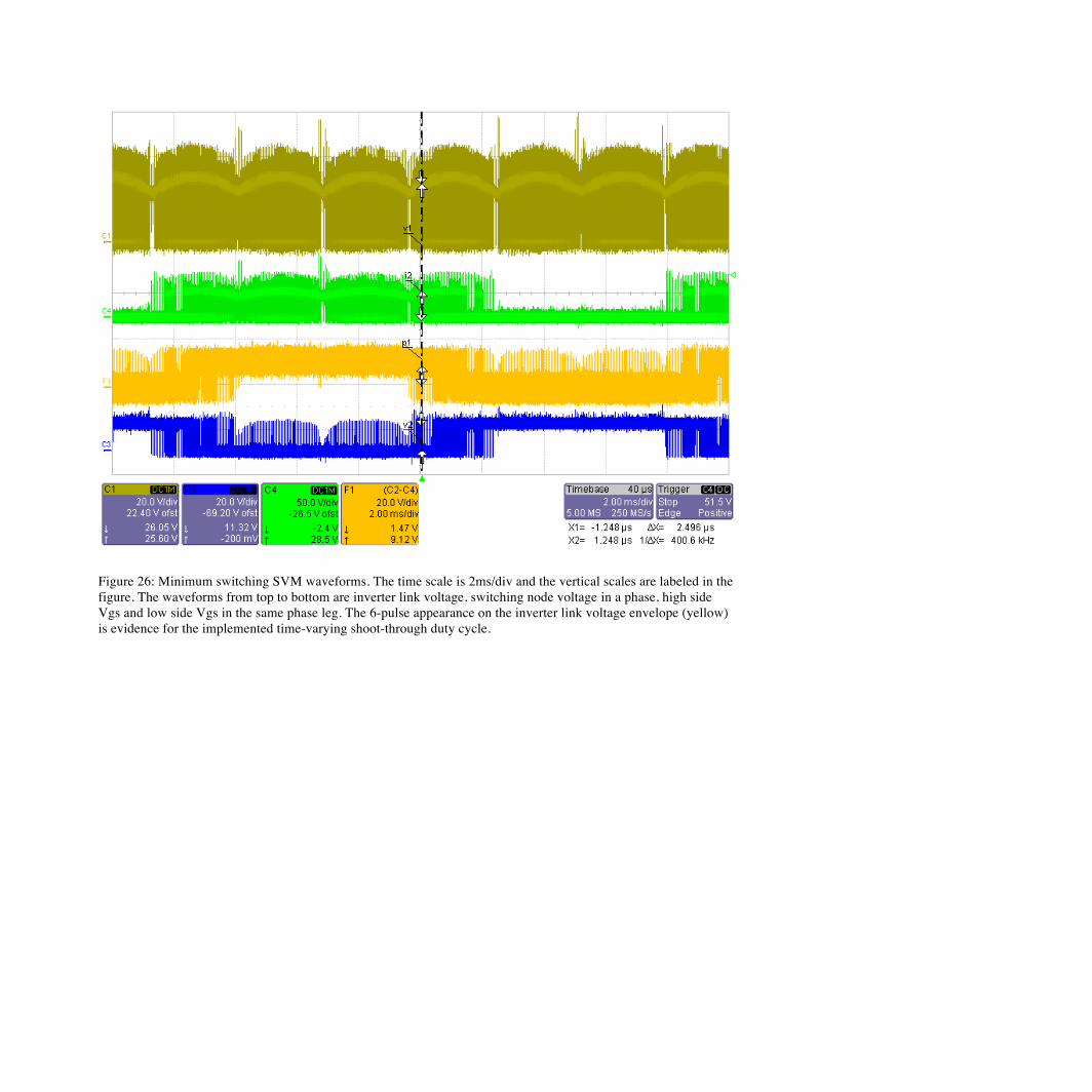
Figure 26: Minimum switching SVM waveforms. The time scale is 2ms/div and the vertical scales are labeled in the figure. The waveforms from top to bottom are inverter link voltage, switching node voltage in a phase, high side Vgs and low side Vgs in the same phase leg. The 6-pulse appearance on the inverter link voltage envelope (yellow) is evidence for the implemented time-varying shoot-through duty cycle.

Fig.27 shows that the minimum switching symmetric SVM reduces the total system loss
by 20% compared to the constant boost SVM in the tests conducted. The loading conditions in
these tests are the same as in Table 4. Input voltages at 24V, 28V, 32V and 36V are used for
each scheme to generate the data points for comparison.
Figure 27: Power Loss Comparison between Minimum Switching SVM and Constant Boost SVM
0
0.01
0.02
0.03
0.04
0.05
0.06
11 12 13 14 15 16 17 18 19OutputPhaseCurrent(Arms)
LossvsOutputPhaseCurrent(Arms)
consBoost
minSwitching

Conclusion
This technical report presents the analysis, circuit design and control design of a Z-source
inverter for an electric bike. The original analysis on ZSI based on differential power provides
insight into the disadvantages of the topology and provides a quantitative measure of the boost
factor that can be practically used. The newly developed minimum switching SVM uses variable
modulation depth and variable boost to reduce converter loss significantly. Due to the
unavailability of a dynamometer, all the experiments were performed on an RL load. However,
the proposed space vector modulation can be easily fitted into a standard field oriented control
scheme for driving AC machines. The minimum switching SVM control used for the initial
performance evaluation only considers a single operating point but it could be easily extended
using the algorithm in Appendix 2.
This project demonstrates that the ZSI is a viable candidate for high performance e-bike
controllers. The use of a ZSI can extend the constant torque region and achieve higher top speed
in an e-bike. Without voltage boost, this could only be achieved by either using larger battery
packs or switching to motors that produce less torque. The main disadvantages of the topology
are the volume and cost of the added passives in the impedance network front-end. If only
modest boost is required (< 2X), which is the case for an e-bike, these disadvantages may be a
small price to pay for the higher performance and more flexibility in designing e-bike systems.

References
[1] F.Z.Peng, “Z-source inverter,” IEEE Trans. Ind. Appl., vol. 39, no. 2, pp. 504–510, 2003.
[2] S.Miaosen, W.Jin, A.Joseph, F.Z.Peng, L.M.Tolbert, and D.J.Adams, “Maximum constant boost control of the z-source inverter,” Proc. IEEE Ind. Appl. Conf., pp. 1–147, 2004.
[3] H. Cha, Y. Li, and F.Z.Peng, “Practical layouts and dc-rail voltage clamping techniques of z-source inverters,” IEEE Trans. Power Electron., vol. 31, no. 11, pp. 7471–7479, 2016.
[4] Y. Siwakoti, F.Z.Peng, F.Blaabjerg, P.C.Loh, G.E.Town, and S.Yang, “Impedance-source networks for electric power conversion part ii: Review of control and modulation techniques,” IEEE Trans. Power Electron., vol. 30, no. 4, pp. 1887–1906, 2015.
[5] F.Z. Peng, M. Shen, and Z. Qian, “Maximum boost control of the z-source inverter,” Proc. of IEEE PESC, 2004.
[6] J.A. Cobos, H. Cristobal, D. Serrano, R. Ramos, J. Oliver and P. Alou. "Differential Power as a metric to optimize power converters & architectures," 2017 IEEEE Energy Conversion Congress and Exposition, ECCE.
[7] M.Olszewski, "Z-Source Inverter for Fuel Cell Vehicles," Michigan State University, East Lansing, MI, Contract DE-AC05-00OR22725, Sep. 2005
[8] J. A. Cobos, “Optimization of Energy Buffered Converters,” 13th International Conference on Power Electronics (CIEP'2016). Guanajuato, Mexico June 20-23, 2016. [9] José A. Cobos, The Google “Little Box Challenge”. UC Berkeley Power Electronics. March 2017. URL: https://www.youtube.com/watch?v=YXBAh8ajwuw

Appendices
1. Differential Power Analysis for ZSI
Each of Inductors L1, L2:
𝑃!"#!_!!" = 𝑉!"# × 𝐼! × 𝑑 = 𝑃! ×𝑑 1− 𝑑1− 2𝑑
Each of Capacitors C1, C2:
𝑃!"#!_!!" = 𝑉!"# × 𝐼! × 𝑑 = 𝑃! ×𝑑 1− 𝑑1− 2𝑑
Capacitor Cin:
𝑃!"##_!"# = 𝑃! × 𝑑

2. Minimum Switching SVM Algorithm
To eliminate all zero states in the control, we can express the output AC magnitude as a function of d the shoot through duty cycle and α the angle labeled in Fig.15a. Note that in the following equations we will assume common mode injection is utilized.
𝑉!" = 𝑀 × 𝐵 × 𝑉!"
3 cos(𝜋6 − 𝛼)
Substituting M = 1-d and B = !!!!!
𝑉!" = 1− 𝑑1− 2𝑑×
𝑉!"3 cos(𝜋6 − 𝛼)
Given a desired AC voltage vector and angle α which is either measured with a hall sensor or estimated with an observer, d can be solved using the above equation.

3. Differential Power Comparison Between Control Methods
For constant boost SVM,
𝑉!" = 1− 𝑑1− 2𝑑×
𝑉!"3
For minimum switching SVM,
𝑉!" = 1− 𝑑1− 2𝑑×
𝑉!"3 cos(𝜋6 − 𝛼)
For a certain !!"!!"
, we can calculate the d for the two control strategies. In the case of minimum
switching SVM, d is a function of 𝛼 as well. The following MATLAB script is used to evaluate
the average differential power of the converters.
%% Appendix 3 Converter Differential Power Calculation under Constant Boost SVM and Minimum Switching SVM
%Comparison based on the example in 3.2
%For constant boost SVM, shoot-through duty cycle is constant at 0.12.
%For minimum switching SVM, shoot-through duty cycle is time-varying and presented in appendix 2
alpha = linspace(0,pi/3,1000); %1000 points from 0 to 60 deg
AF = cos(pi/6-alpha); %AF = angle factor, calculated for ease of calculation later
ST_duty_cycle = (AF*2/sqrt(3) - 1)./(AF*4/sqrt(3)-1); %Time-varying ST duty cycle for the example
Pint_ZSI = @(ZSI_d) ((2*(1-ZSI_d).*ZSI_d./(1-2*ZSI_d))+(2*ZSI_d.*(1-ZSI_d))./(1-2*ZSI_d)+ZSI_d); %Converter Differential Power as a function of ST duty cycle
Max_ST_dutyCycle = max(ST_duty_cycle);
Min_ST_dutyCycle = 0;
Pint_consboost_worst = Pint_ZSI(Max_ST_dutyCycle);
Pint_consboost_best = Pint_consboost_worst;

Pint_consboost_average = Pint_consboost_worst;
Pint_minsw_worst = Pint_ZSI(Max_ST_dutyCycle);
Pint_minsw_best = Pint_ZSI(Min_ST_dutyCycle);
Pint_minsw_average = mean(Pint_ZSI(ST_duty_cycle));
fprintf('Average normalized differential power for constant boost is %d and that for minimum switching is %d\n',Pint_consboost_average,Pint_minsw_average);
%% Instead of working on this specific example, examine general case; want to plot average diff power vs AC magnitude for these two modulation strategies
d_array = [];
for i = 0.667:0.01:2
syms d
eqn = (1-d)/(sqrt(3)*(1-2*d)) == i;
sol_d = solve(eqn,d);
d_array = [d_array,sol_d];
end
Pint_consboost_average_array = Pint_ZSI(d_array);
Vac_over_Vin = 0.667:0.01:2;
plot(Vac_over_Vin,Pint_consboost_average_array)
%%
Pint_minsw_average_array = [];
for i = 0.667:0.01:2
syms d
d_period = [];
for alpha = 0:pi/300:pi/3
AF = cos(pi/6-alpha);
eqn = (1-d)/(sqrt(3)*(1-2*d)*AF) == i;
sol_d = solve(eqn,d);

d_period = [d_period,sol_d];
end
Pint_minsw_average_each = mean(Pint_ZSI(d_period));
Pint_minsw_average_array = [Pint_minsw_average_array,Pint_minsw_average_each];
end
Vac_over_Vin = 0.667:0.01:2;
plot(Vac_over_Vin,Pint_minsw_average_array)


