A11100 ^flb7B3NBS
PUBLICATIONS
NBSIR 79-1748
Detection of Phosphorus in
Epitaxial Silicon by EPR
Te-Tse Chang
Electron Devices Division
Center for Electronics and Electrical
Engineering
National Bureau of Standards
Washington, DC 20234
May 1979
Too. 1)56
79-1748
Prepared for
U.S. Army ERADCOMNight Vision and Electro-optics Laboratory
Ft. Belvoir, VA 22060

1'j

National Bureau of Stands
JUN 2 1 J97g
NBSIR 79 1748
DETECTION OF PHOSPHORUS IN
EPITAXIAL SILICON BY EPR
Te-Tse Chang
Electron Devices Division
Center for Electronics and Electrical
Engineering
National Bureau of StandardsWashington, DC 20234
May 1979
Prepared for
U.S. Army ERADCOMNight Vision and Electro-optics LaboratoryFt. Belvoir, VA 22060
U.S. DEPARTMENT OF COMMERCE, Juanita M. Kreps, Secretary
Jordan J. Baruch, Assistant Secretary for Science and Technology
NATIONAL BUREAU OF STANDARDS. Ernest Ambler. Director


TABLE OF CONTENTS
Page
Abstract 1
I . I ntroduction 1
I I . Background 2
a. Unpaired Electrons in Magnetic Field 2
b. Localized Conduction Electrons in n- type Si 3
ill. Experimental Results 5
IV. Conclusion 8
V. Acknowledgement 8
V I . References 9
Di stri bution 10
iii

LIST OF FIGURES
Page
1. The Zeeman energy level diagram of an unpaired electron. Thehorizontal axis is the magnetic field, the vertical axis is
the energy, both in arbitrary units 3
2. The Zeeman energy level diagram of an electron associatedwith a nucleus of spin 1/2. Ms is the magnetic quantumnumber of the electronic spin, M| is the magnetic quantumnumber of the nuclear spin 4
3. The EPR spectrum from phosphorus doped silicon. The temper-ature is 4.2 K 6
4. The EPR spectrum from the epitaxial layer of indium dopedsilicon. The arrows point to the peaks identified as thecontribution from phosphorus ions 7
iv
Detection of Phosphorus in Epitaxial Silicon by EPR
Te-Tse ChangElectron Devices Division
National Bureau of StandardsWashington, DC 2023^
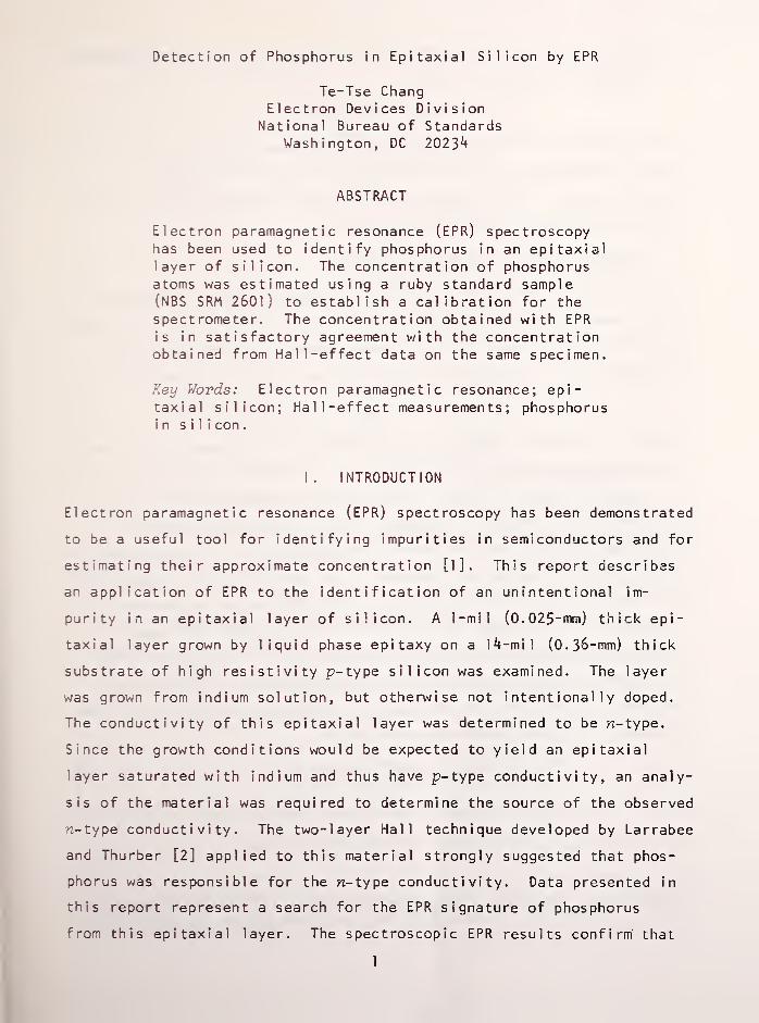
ABSTRACT
Electron paramagnetic resonance (EPR) spectroscopyhas been used to identify phosphorus in an epitaxiallayer of silicon. The concentration of phosphorusatoms was estimated using a ruby standard sample(NBS SRM 2601) to establish a calibration for the
spectrometer. The concentration obtained with EPRis in satisfactory agreement with the concentrationobtained from Hall-effect data on the same specimen.
Key Words: Electron paramagnetic resonance; epi-taxial silicon; Hall-effect measurements; phosphorusin s i 1 i con
.
I. INTRODUCTION
Electron paramagnetic resonance (EPR) spectroscopy has been demonstrated
to be a useful tool for identifying impurities in semiconductors and for
estimating their approximate concentration [1]. This report describes
an application of EPR to the identification of an unintentional im-
purity in an epitaxial layer of silicon. A 1-mil (0.025~mm) thick epi-
taxial layer grown by liquid phase epitaxy on a 14-mil (0.36-mm) thick
substrate of high resistivity p- type silicon was examined. The layer
was grown from indium solution, but otherwise not intentionally doped.
The conductivity of this epitaxial layer was determined to be n-type.
Since the growth conditions would be expected to yield an epitaxial
layer saturated with indium and thus have p- type conductivity, an analy-
sis of the material was required to determine the source of the observed
n- type conductivity. The two-layer Hall technique developed by Larrabee
and Thurber [2] applied to this material strongly suggested that phos-
phorus was responsible for the n-type conductivity. Data presented in
this report represent a search for the EPR signature of phosphorus
from this epitaxial layer. The spectroscopic EPR results confirm' that
1

the impurity giving rise to the rc-type conductivity is indeed phosphorus
as inferred from the Hall data.
II. BACKGROUND
A few aspects of EPR spectroscopy that are essential for the identifi-
cation of phosphorus ions in silicon will be described briefly in
"liberal terms". For a rigorous and complete treatment of the subject,
there are excellent treatises available [ 3 ]
•
a. Unpaired Electrons in Magnetic Field.
When an unpaired electron is placed in a magnetic field, the magnetic
dipole moment of the electron will align itself either parallel or anti-
parallel to the magnetic field. Hence, there are two energy states
(see figure 1). The spacing between the two states is given by
hv = g3H (1
)
where h is Planck's constant, v is the transition frequency, g is the
Lande spectroscopic splitting factor, 3 is the Bohr magneton, and H is
the external magnetic field. In a transition between the two states
electromagnetic energy of frequency v will be absorbed or emitted.
Since the frequency and the external magnetic field can be measured, and
since h and 3 are universal constants, the value of g can be determined
experimentally. For free electrons, g = 2.0023, which corresponds to a•“V
transition of v = 9-5 GHz at a magnetic field of about 3420 gauss.
Conduction electrons in silicon are subject to the crystalline field
and therefore behave according to the band structure of the crystal
.
They are not free, and the g- factor is different from that of the free
electrons. The best measured value [4] is
gcE= K"875 1 0 - 00010 - (2)
This difference in g-value will shift the resonance magnetic field
about 8 gauss at a resonance frequency of 9-5 GHz.
"Gauss" is a customary unit to measure magnetic field in EPR spectros-copy. "Gauss" has the same magnitude as "Oersted" in vacuum, which is
equivalent to 10-4
Tesla.
2
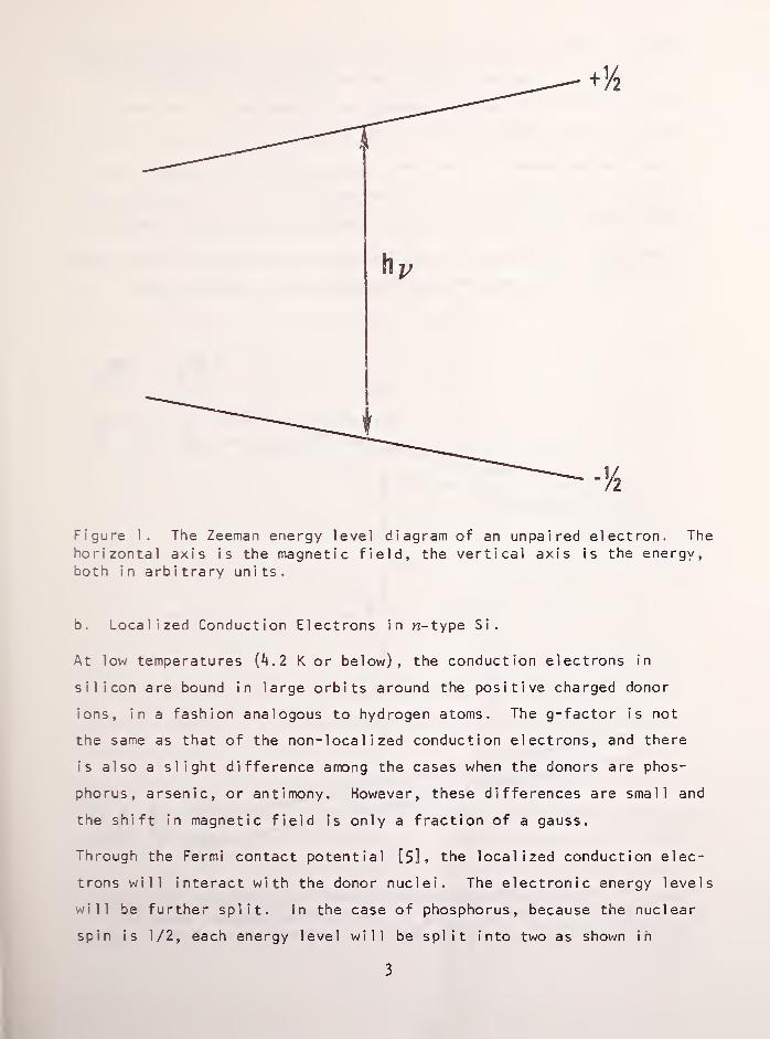
Figure 1. The Zeeman energy level diagram of an unpaired electron. Thehorizontal axis is the magnetic field, the vertical axis is the energy,both in arbitrary units.
b. Localized Conduction Electrons in n-type Si.
At low temperatures (A. 2 K or below), the conduction electrons in
silicon are bound in large orbits around the positive charged donor
ions, in a fashion analogous to hydrogen atoms. The g-factor is not
the same as that of the non- 1 oca 1 i zed conduction electrons, and there
is also a slight difference among the cases when the donors are phos-
phorus, arsenic, or antimony. However, these differences are small and
the shift in magnetic field is only a fraction of a gauss.
Through the Fermi contact potential [ 5 ], the localized conduction elec-
trons will interact with the donor nuclei. The electronic energy levels
will be further split. in the case of phosphorus, because the nuclear
spin is 1/2, each energy level will be split into two as shown in
3

figure 2. During an electronic transition, the nuclear states usually
do not change. Thus two transitions are possible as indicated in
figure 2, and the selection rules AM^ = ± 1, and AM^. = 0 are obeyed.
The EPR spectrum should appear as two absorption lines.
In the case of arsenic, since the nuclear spin is 3/2, each of the
electronic levels will be split into four (21 + 1 = 4). The spectrum
should appear as four lines of equal separation and equal intensity.
For antimony, the isotropic distribution is 57.25% spin 5/2, and 42.75%
spin 7/2 [6]. The spectrum should appear as six lines and eight
M s
+J4
Figure 2. The Zeeman energy level diagram of an electron associatedwith a nucleus of spin 1/2. Ms is the magnetic quantum number ofthe electronic spin, Mj is the magnetic quantum number of the nuclear
spin.
4

lines superimposed. The members of the six line group should be about
twice as intense as the members of the eight lines.
III. EXPERIMENTAL RESULTS
The EPR spectrometer is of conventional homodyne design, operated at
9-5 GHz. All the experiments were performed at a temperature of -k 2 K.
The spectrometer is able to detect the EPR absorption from a sample of
10** active spins provided the corresponding E P R absorption line is one
gauss wide. From Hall measurements, the concentration of phosphorus
ions in the epitaxial layer was estimated to be about 10 17 cm 3. The
specimen available for EPR experiments was about 0.25 cm 2 in area, and
the epitaxial layer was about 2.5 x 1 0 3 cm thick. The total number of
spins available tc be detected in the specimen was thus estimated to be
about 6 x 10 13. However, since there are two phosphorus lines, and
each is about three to four gauss wide, it was necessary to operate the
spectrometer near the limit of its sensitivity and some experimental
precautions were required.
First, the spectrometer was operated using a specimen of phosphorus-
doped silicon in which the total number of phosphorus ions was known to
be about 10 lp. The characteristic spectrum of electrons bound to phos-
phorus ions was observed as shown in figure 3. The two hyperfine lines
as discussed above are resolved; the spacing about ^0 gauss. The
weak absorptions between the two lines are due to the clustering of
phosphorus ions, that enables the orbit of the electron to enclose two
or more phosphorus ions. From these observations, the range of the
resonance magnetic field and the expected pattern of the absorption
1 i nes was known
.
The specimen of the silicon epitaxial layer was then placed in the
sample cavity of the spectrometer along with a ruby standard sample [7].
The ruby SRM has a total of 1 x 10 16 Cr3+
ions with spin 3/2. A weak
transition of Cr 3+
(the active specie of the ruby SRM) was selected,
the intensity of which is about 0.003 of the major (1/2, - 1/2)
transition. This spectral line of the SRM is equivalent in strength
to 3 x 10 13 spins. The spectrometer could register this transition as
5

Figure 3. The EPR spectrum from phosphorus doped silicon. Thetemperature is k.2 K.
6
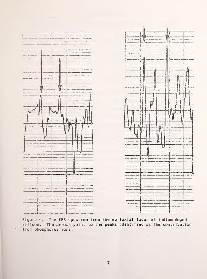
Figure 4. The EPR spectrum from the epitaxial layer of indium dopedsilicon. The arrows point to the peaks identified as the contributionfrom phosphorus ions.
7
a full scale signal. Then the desired range of the magnetic field for
the phosphorus resonance was searched with a slow sweeping rate
('v 1 G/min), and a long lock-in amplifier integration time (10 s)
.
The signal from the epitaxial layer was observed under the above
conditions. The results of the two best sweeps are shown in figure 4.
The arrows point to the phosphorus signal, the intensity of which is
about one tenth of that of the selected transition of the ruby SRM.
The backgrounds are not random. They may be the contribution from
clustered phosphorus ions, non-local i zed conduction electrons, or other
donors in the layer.
IV. CONCLUSION
The presence of phosphorus ions in the epitaxial layer was confirmed
from the result of this experiment. The concentration of phosphorus
ions was estimated to be about IQ 16 cm" 3 from the intensity of the EPR
line. Since the signal was weak and the background intense, an accurate
measurement of the concentration was not possible. The lines were about
ten gauss wide, which is broader than that from the reference sample.
This may be due to the fact that the spins are residing in a thin layer,
or some unknown mechanism may broaden the EPR absorption lines. It may
be possible that the contributions from some of the spins are too broad
to be observable. Because of these considerations, it is conceivable
that the estimate of the concentration could be off by an order of
magnitude, and hence the 10 16 cm-3
value should be considered as a
lower bound, in satisfactory agreement with 10 17 cm" 3 from the Hall
measurements [2].
V. ACKNOWLEDGEMENT
Dr. Barbara E. Sumner of the Night Vision and Electro-optics Laboratory,
Ft. Belvoir, VA provided the specimen studied in this report and useful
technical discussions. Technical discussions with R. D. Larrabee and
W. R. Thurber are also gratefully acknowledged.
VI. REFERENCES
1. See for example: Alger, R. S., Electron Paramagnetic Resonance:Techniques and Applications (Interscience, New York, NY, 1 968 )
.
2. Larrabee, R. D. and Thurber, W. R., Theory and Application of a
Two-Layer Hall Technique, NBSIR 78-1553, October 1978.
3. See for example: Poole, Jr., C. P., Electron Spin Resonance,(Interscience, New York, NY, 1967); Poole, Jr., C. P. and Farach,H. A., The Theory of Magnetic Resonance, (Wi ley- Interscience, NewYork, NY, 1972).
4. Feher, G.,Electron Spin Resonance Experiments on Donors in Silicon
I. Electronic Structure of Donors by the Electron Nuclear DoubleResonance Technique, Phys. Rev. 114 , 1 2 1
9
-1 244 ( 1 959)
-
5. Fermi, E., Uber die magnetischen Momente der Atomkerne, Z. Phys.
60, 320-333 (1930).
6. Weast, R. C., Handbook of Chemistry and Physics, pp. B- 333, B-334(The Chemical Rubber Company, 1 890 1 Cranwood Parkway, Cleveland, OH
44128).
7- Chang, T. and Kahn, A. H.,Electron Paramagnetic Resonance Intensity
Standards: SRM 2601; Description and Use, NBS Special Publication260-59 (U. S. Department of Commerce/National Bureau of Standards,Washington, DC 20234, August 1978).
9

NBS-1I4A (REV. B-76)
U.S. DEPT. OF COMM.
BIBLIOGRAPHIC DATASHEET
1. PUBLICATION OR REPORT NO.
NBSIR 79-1748
i. pleat* Accession No.
4. TITLE AND SUBTITLE
Detection of Phosphorus in Epitaxial Silicon by EPR
5. Publication Date
May 1979
7. AUTHOR(S) 8. Performing Organ. Report No.
Te-Tse Chang
9. PERFORMING ORGANIZATION NAME AND ADDRESS
NATIONAL BUREAU OF STANDARDSDEPARTMENT OF COMMERCEWASHINGTON, DC 20234
11. Contract/Grant No.
MERADCOM 28052
12. SPONSORING ORGANIZATION NAME AND COMPLETE ADDRESS fSfreaf, city, state, ZIP)
U.S. Army ERADCOMNight Vision and Electro-optics LaboratoryFt. Belvoir, VA 22060
13. Type of Report & Period Covered
15. SUPPLEMENTARY NOTES
Conducted as part of the NBS Semiconductor Technology Program.
| |Document describes a computer program; SF-185, FIPS Software Summary, is attached.
16. ABSTRACT (A 200-word or less factual aummary of moat significant information. If document includes a significant bibliography or
literature survey, mention it here.)
Electron paramagnetic resonance (EPR) spectroscopy has been used to identifyphosphorus in an epitaxial layer of silicon. The concentration of phosphorusatoms was estimated using a ruby standard sample (NBS SRM 2601) to establish a
calibration for the spectrometer. The concentration obtained with EPR is in
satisfactory agreement with the concentration obtained from Hall'-effect data on
the same specimen.
17. KEY WORDS (six to twelve entries; alphabetical order; capitalize only the first tetter of the first key word unless a proper name;separated by semicolons)
Electron paramagnetic resonance; epitaxial silicon; Hall-effect measurements;
phosphorus in silicon.
18. AVAILABILITY H Unlimited
n For Official Distribution. Do Not Release to NTIS
[ |Order From Sup. of Doc., U.S. Government Printing Office, Washington, DC20402, SD Stock No. SN003-003-
(x~l Order From National Technical Information Service (NTIS), Springfield,
VA. 22161
19. SECURITY CLASS(THIS REPORT)
UNCLASSIFIED
20. SECURITY CLASS(THIS PAGE)
UNCLASSIFIED
21. NO. OFPRINTED PAGES
15
22. Price
$4.00
USCOMM* DC