
1 | P a g e
DEVBHOOMI INSTITUTE OF TECHNOLOGY FOR WOMEN,
DEHRADUN - 248407
DEPARTMENT OF ELECTRONICS AND COMMUNICATION
ENGINEERING
Prepared BY:
Ajay Kumar Gautam
Asst. Prof.
Electronics & Communication Engineering Department
OFC & VLSI SIMULATION LAB MANUAL

2 | P a g e
PEC-753 OFC & VLSI SIMULATION LAB
Design of following ckt using appropriate software like VHDL/ FPGA and OFC kits
1) 3-input NAND gate.
2) Half adder, Full Adder
3) D-Latch, T Flip Flop
4) Serial in-serial out shift register, Bidirectional shift Register
5) 3 Bit synchronous counter
6) To set up Fiber Optic Analog link.
7) To set up fiber Optic Digital link.
8) Measurement of Propagation loss and numerical aperture.
9) Characterization of laser diode and light emitting diode.

3 | P a g e
EXPERIMENT 01
SETTING UP FIBER OPTIC ANALOG LINK
OBJECTIVE:
The objective of this experiment is to study a 650 nm fiber optic
analog link. In this experiment, we will study a relationship between the input signal
and the received signal.
PROCEDURE:
1. Connect the power supply to the board.
2. Ensure that all switch faults are OFF.
3. Make the following connections.
a. Connect the function generator 1 KHz sine wave output to the emitter
1’s input.
b. Connect the fiber optic cable between the emitter’s output and
detector’s input.
c. Connect detector’s output to the AC amplifier 1’s input.
4. On the board switch emitter 1’s driver to analog mode.
5. Switch ON the power.
6. Observe the input to emitter (tp 5) with output from AC amplifier 1 (tp 28)
and note that the two signals are same.
RESULT:
Thus the relationship between input and output waves was obtained.

4 | P a g e
SETTING UP FIBER OPTIC ANALOG LINK
Emitter circuit Detector circuit
Function Generator AC Amplifier
1 KHz Circuit
OBSERVATION
Input Voltage
(V)
Output Voltage
(V)
Time
(ms)
Gnd

5 | P a g e
EXPERIMENT 02
SETTING UP FIBER OPTIC DIGITAL LINK
OBJECTIVE:
The objective of this experiment is to study a 650 nm fiber optic digital
link. In this experiment, we will study a relationship between the input signal and the
received signal.
PROCEDURE:
7. Connect the power supply to the board.
8. Ensure that all switch faults are OFF.
9. Make the following connections.
a. Connect the function generator 1 KHz square wave output to the
emitter 1’s input.
b. Connect the fiber optic cable between the emitter’s output and
detector’s input.
c. Connect detector 1’s output to the comparator 1’s input.
d. Connect comparator 1’s output to AC amplifier 1’s input.
10. On the board switch emitter 1’s driver to digital mode.
11. Switch ON the power.
12. Monitor both the inputs to comparator 1 (tp 13 and tp 14). Slowly adjust the
comparator bias. Reset until DC level on the input (tp 13) lies midway
between the high and low level of the signal on positive input (tp 14).
13. Observe the input to emitter (tp 5) with output from AC amplifier 1 (tp 28)
and note that the two signals are same.
RESULT:
Thus the relationship between input and output waves was obtained.
Frequency (KHz) =

6 | P a g e
SETTING UP FIBER OPTIC DIGITAL LINK
Emitter circuit Detector circuit
AC amplifier
Circuit
OBSERVATION
Input Voltage
(V)
Output Voltage
(V)
Time
(ms)
Function
Generator
1 KHz
Comparator
Gnd

7 | P a g e
EXPERIMENT 03
STUDY OF PROPAGATION LOSS IN OPTICAL FIBRE
Objective:
The objective of this experiment is to measure the propagation loss and the
bending loss in the optical fibre.
Theory:
Attenuation loss (or path propagation loss) is the reduction in power density
(attenuation) of an electromagnetic wave as it propagates through space. Attenuation
loss is a major component in the analysis and design of the link budget of a
telecommunication system.
Attenuation occurring as a result of either a bend in an optical fibre that
exceeds the minimum bend radius or an abrupt discontinuity in the core/cladding
interface is called bending loss. The incident light rays strike the boundary between
the core and the cladding at an angle less than the critical angle and enter the
cladding, where they are lost
Procedure:
i)To find propagation loss:
1. Connect the power supply to the board.
2. Make the following connections
a) Function generators 1KHz sinewave output to input 1 socket of emitter 1 circuit
via 4mm lead.
b) Connect 0.5m optic fibre between emitter 1 output and detector 1’s input.
c) Connect detector 1 output to amplifier 1 input socket via 4mm lead.
3. Switch ON the power supply.
4. Set the oscilloscope channel 1 to 0.5V /div and adjust 4-6 div amplitude by using
x1 probe with
the help of variable pot in function generator block input 1 of emitter 1.
5. Observe the output signal from detector t p 10 on CRO.
6. Adjust the amplitude of the received signal as that of transmitted one with the help
of gain adjust
pot in AC amplifier block. Note this amplitude and name it V1.

8 | P a g e
7. Now replace the previous FO cable with 1m cable without disturbing any previous
setting.
8. Measure the amplitude at the receiver side again at output of amplifier 1 socket t p
28. Note this value and name it V2.
9. Calculate propagation (attenuation) loss with the help of following formula
V1/V2 = exp(-α(L1+L2))
Where α is loss in nepers/m
1 neper = 8.686dB
L1 = length of shorter cable (0.5m)
L2 = length of longer cable (1m)
ii)To find bending loss
1. Repeat all steps from 1-6 of the above procedure using 1m cable.
2. Wind FO cable on the Mandrel and observe the corresponding AC amplifier
output on CRO.
It will be gradually reducing showing loss due to bends.
Block diagram: Study of Propagation Loss
Study of Bending Loss

9 | P a g e
Results: Thus the propagation and bending losses in the fibre optic was measured and
studied by this experiment.

10 | P a g e
EXPERIMENT 04
NOR & NAND Implementation
Objectives:
• To demonstrate the implementation of a digital system sing NAND and NOR
gates.
Background Information:
NAND and NOR gates is said to be universal gates because any digital
system can be implemented using only one of these gates.
Digital circuits are frequently constructed with only NAND or NOR gates;
because these gates are easier to fabricate with electronic components. Because
of the importance of NAND and NOR in the design of digital circuits, rules and
procedures have been developed for the conversion from Boolean functions in
terms of AND, OR and NOT into equivalent NAND or NOR logic diagrams.
NAND and NOR are called universal gates because any digital system or
Boolean function can be implemented with only these gates.
From DeMorgan theorem, we can see other representation for NAND and NOR
gates as follows:

11 | P a g e
Equipment Requires:
The following equipments are needed to perform all the procedures :
Universal Breadboard
Jumper wire kit
(1) 7400 TTL QUAD 2-INPUT NAND GATE
(1) 7402 TTL QUAD 2-INPUT NOR GATE
(1) 7410 TTL TRIPLE 3-INPUT NAND GATE
(1) 7427 TTL TRIPLE 3-INPUT NOR GATE
2x Toggle Switches
1x Carbon-film Resistor (470Ω)
1x LED
Procedure:
1. Using only NAND and NOR gates to implement all basic logic gates and then
verify your results.

12 | P a g e
2. NAND Implementation of Boolean functions:
� Assume that all variables and their complements are available as inputs.
� Find the minimum SOP expression of the function.
� Draw the corresponding two-level AND-OR circuit diagram.
� Replace all gates with NAND gates; learning the gates interconnections are
kept unchanged.

13 | P a g e
EXPERIMENT 04
SHIFT REGISTERS
1. Introduction
Shift registers are specialized memory systems composed of flip-flops or other
types of memory cells. The distinguishing feature of shift registers is that data can
be transferred on command from one cell to the adjacent memory cell as many
times as needed.
The simplest shift registers will transfer one data bit in for each clock cycle
until the register capacity is reached. At this time the register contents may be
sampled.
More complex registers will allow direct sampling of each output stage so that
the register contents can be examined on each clock cycle. Other registers allow
parallel loading where the entire register is loaded at once.
A special type of shift register known as the universal shift register will shift
entries left or right, and input or output data serially or parallel. Shift registers
may be constructed from either J-K flip-flops as shown in Figure below.
Figure J-K flip-flop Shift Register
Figure D flip-flop Shift Register
The single data input of the shift register in Figure.1 is known as a single rail
input. If the J and K inputs are used as separate data inputs then the shift register
output
Clock
output
Serial input
Parallel
SerialQJ
Q
CLK
K
QJ
Q
CLK
K
QJ
Q
CLK
Serial input
Clock
Serial outputD Q
CLK
D Q
CLK
D Q
CLK

14 | P a g e
is said to have a dual rail input. Likewise if the shift register uses both the true
and complement outputs the circuit is called a dual rail output circuit. Of course
if only one of the outputs is used then the circuit is described as having a single
rail output. Note that the output of the J-K shift register shown can be either
serial or parallel. Shift registers can be classified as :
a. Serial-in/serial-out : SISO
b. Serial-in/parallel-out : SIPO
c. Parallel-in/serial-out : PISO
d. Parallel-in/parallel-out : PIPO
All parallel input registers can be operated as serial input registers and the
same is true for output. The reverse situation is not true in that serial input
registers cannot be operated as parallel input registers.
Johnson Counter :
Shift registers can be used to form a special kind of counter known as a ring
counter. A ring counter works by loading a binary ONE into the input flip-flop of
a shift register and tying the register output to the input. When the register is
clocked the ONE will move through the register one cell at a time. After a
number of clock pulses equal to the number of cells in the register, the ONE will
circuit back to the input flip-flop.
This allows a form of counting. This type of counter uses more flip-flops than
required to perform the count. For example, three flip-flops configured as a ring
counter can have only three states or counts while a binary counter with three
flip-flops can count eight states when properly decoded.
The advantage of the ring counter is that no decoding is required to determine
the count. The ring counter has 2N-N disallowed states where that N is the
number of flip-flops. A special type of ring counter is the Johnson counter.
The Johnson counter has the output inverted before it is fed back into the input
so that the maximum count is 2·N with N being the number of flip-flops. This, of
course means that the Johnson counter has (2N)-(2 · N) disallowed states. The
Johnson counter makes better use of the flip-flops than a simple ring counter and
it also can be decoded by using a two-input AND for each decoded output.
Schematic for a 3-flip-flop Johnson counter is shown in Figure.6.3.
Figure Johnson counter
2. Exercises
2.1. Objective
Q1 Q2 Q3
Q1' Q2' Q3'
Clock
D Q
CLK
Q
D Q
CLK
Q
D Q
CLK
Q

15 | P a g e
The purpose of this lab is to investigate shift registers. We will implement
shift register and johnson counter using discrete flip-flop ICs..
2.2. Materials
2x74LS74 Dual D-Type Positive Edge-Triggered Flip-Flop
1x74LS174 Hex D Flip-Flop
2x74LS08 Quadruple 2 Input Positive AND Gate
1x74LS32 Quadruple 2 Input Positive OR Gate
2.3. Procedure
1. Set up the circuit shown in Figure.
Figure Shift Register
2. Turn on power. Turn switch1 to logic-1 position..
3. Use switch2 as the input bit, PB2 as the clock input and Led1-Led4 as the
output.
4. Reset the outputs of the register using switch1.
5. Fill in the following table.
Serial input
(Switch2)
Reset input
(Switch1)
Clock pulse
(PB2) Led1 Led2 Led3 Led4
x 0
1 1
0 1
1 1
1 1
x = Don't care.
6. Connect the complement output of the fourth flip-flop to the input of the first
flip-flop. This counter is called Johnson counter.
7. Reset the outputs of the counter.
8. Rotate the single bit with the shift condition. Observe and record the state of
the register after each clock pulse.
PB2Clock
switch1 (reset)
switch2 (serial input)
led1 led2 led3 led4
D2
CLK3
Q5
Q6
CL
1
D12
CLK11
Q9
Q8
CL
7
D2
CLK3
Q5
Q6
CL
1
D12
CLK11
Q9
Q8
CL
7
D1 D2 D3 D4
16 | P a g e
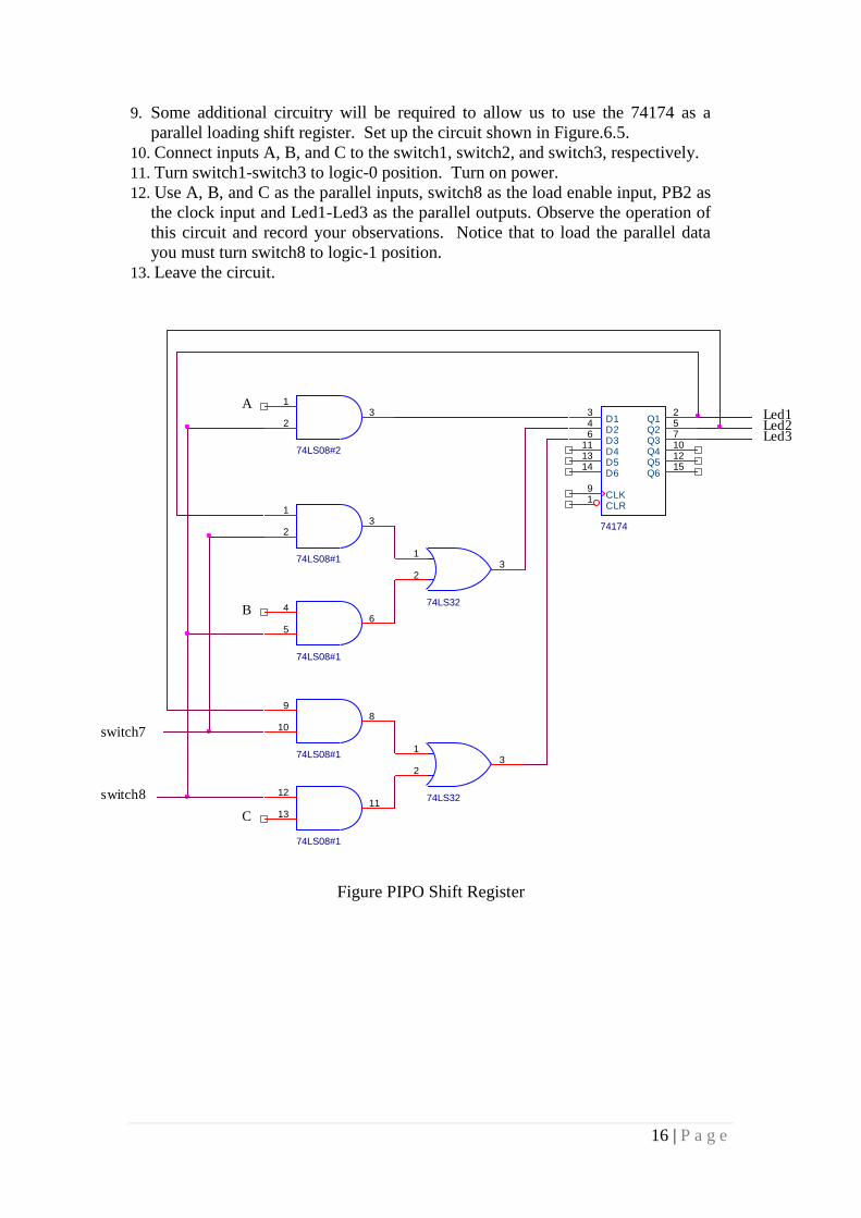
9. Some additional circuitry will be required to allow us to use the 74174 as a
parallel loading shift register. Set up the circuit shown in Figure.6.5.
10. Connect inputs A, B, and C to the switch1, switch2, and switch3, respectively.
11. Turn switch1-switch3 to logic-0 position. Turn on power.
12. Use A, B, and C as the parallel inputs, switch8 as the load enable input, PB2 as
the clock input and Led1-Led3 as the parallel outputs. Observe the operation of
this circuit and record your observations. Notice that to load the parallel data
you must turn switch8 to logic-1 position.
13. Leave the circuit.
Figure PIPO Shift Register
PB2(Clock)
A
switch8
B
C
Led1Led2Led3
74174
D13
D24
D36
D411
D513
D614
CLK9
CLR1
Q12
Q25
Q37
Q410
Q512
Q615
74LS08#1
1
23
74LS08#1
4
56
74LS08#1
9
108
74LS08#1
12
1311
74LS08#2
1
23
74LS32
1
23
74LS32
1
23
switch7

17 | P a g e
EXPT NO. 5
DESIGN OF ADDER AND SUBTRACTOR
AIM:
To design and construct half adder, full adder and verify the truth
table using logic gates.
APPARATUS REQUIRED:
Sl.No. COMPONENT SPECIFICATION QTY.
1. AND GATE IC 7408 1
2. X-OR GATE IC 7486 1
3. NOT GATE IC 7404 1
4. OR GATE IC 7432 1
3. IC TRAINER KIT - 1
4. PATCH CORDS - 23
THEORY:
HALF ADDER:
A half adder has two inputs for the two bits to be added and two
outputs one from the sum ‘ S’ and other from the carry ‘ c’ into the higher
adder position. Above circuit is called as a carry signal from the addition
of the less significant bits sum from the X-OR Gate the carry out from the
AND gate.

18 | P a g e
FULL ADDER:
A full adder is a combinational circuit that forms the arithmetic
sum of input; it consists of three inputs and two outputs. A full adder is
useful to add three bits at a time but a half adder cannot do so. In full
adder sum output will be taken from X-OR Gate, carry output will be
taken from OR Gate.
LOGIC DIAGRAM:
HALF ADDER
TRUTH TABLE:
A B CARRY SUM
0
0
1
1
0
1
0
1
0
0
0
1
0
1
1
0
K-Map for SUM: K-Map for CARRY:

19 | P a g e
SUM = A’B + AB’ CARRY = AB
LOGIC DIAGRAM:
FULL ADDER
FULL ADDER USING TWO HALF ADDER
TRUTH TABLE:
A B C CARRY SUM
0
0
0
0
1
1
1
1
0
0
1
1
0
0
1
1
0
1
0
1
0
1
0
1
0
0
0
1
0
1
1
1
0
1
1
0
1
0
0
1

20 | P a g e
K-Map for SUM:
SUM = A’B’C + A’BC’ + ABC’ + ABC
K-Map for CARRY:
CARRY = AB + BC + AC

21 | P a g e
Experiment 6
D Flip-Flop
Objectives: To build and utilize a D flip-flop circuit.
Required Equipment: The MultiSIM software, 74LS series chips, one
switch/LED box, 5V power supply, breadboard and wires.
Preparatory Exercises:
Review the operation and uses for D flip-flops in your digital logic design texts.
Also review the specifications for the 74LS74 IC in the TTL data sheets.
1. Give a brief description of the use of D flip-flops in logic design.
2. Develop a 74LS74 D flip-flop using 2-input and 3-input NAND gates.
Simulate it using MultiSIM. Submit a clearly labeled circuit diagram.
3. For the circuit developed in Exercise 2, calculate the worst-case
propagation delay from positive edge of clock to outputs, and from reset
and preset inputs to outputs. In addition, calculate the worst-case data
setup time for input D relative to positive edge of clock.
4. In the design above, beginning in each case from reset:
What happen if D=1and a clock pulse occurs?
What happen if D=0 and a clock pulse occurs?
5. Connect the designed circuit using TTL NAND IC’s and be prepared to
operate the circuit using the switch/LED boxes during the lab.
Laboratory Procedure:
1. Simulate the circuit developed above with MultiSIM using NAND IC’s.
2. Using the circuit designed and assembled in the Preparatory Exercises,
correct any design errors, and demonstrate the operation of the circuit.
3. The switch/LED boxes will be available during the lab for debugging and
demonstration purposes.
4. The circuits should perform all the functions provided by the 74LS74 gates
including the set and reset.
5. Treat all incoming signals including the clock as inputs controlled by the
switch box and both Q and Q’ as outputs to the LEDs.
6. Demonstrate proper operation of the circuit to the lab instructor.
Report Contents:
1. A title page (including course name, experiment number and name,
instructor’s name, group number, student names, and date)
2. Answer of the above preparatory exercises.
3. A description of the process in sufficient detail for a reader without the
assignment sheet to be able to follow the design from inception to
completion.
4. A circuit diagram for the circuit and any requested tables, diagrams, and
calculations.
5. Comments on the experiment including any difficulties encountered.
Report Preparation: All material included should be presented in neat and
orderly fashion. Use of a word processor and drawing package is required.


