TEL AVIV UNIVERSITY THE IBY AND ALADAR FLEISHMAN FACULTY OF ENGINEERING
Developing of Advanced Sputtering Methods
By
Alexander Axelevitch
THESIS SUBMITTED DOR THE DEGREE OF "DOCTOR OF PHYLOSOPHY"
SUBMITTED TO THE SENATE OF TEL-AVIV UNIVERSITY
December 2001

TEL AVIV UNIVERSITY THE IBY AND ALADAR FLEISHMAN FACULTY OF ENGINEERING
Developing of Advanced Sputtering Methods
By
Alexander Axelevitch
THESIS SUBMITTED DOR THE DEGREE OF "DOCTOR OF PHYLOSOPHY"
SUBMITTED TO THE SENATE OF TEL-AVIV UNIVERSITY
This Research Work was Carried Out at Tel-Aviv University in The Faculty Of Engineering
Under The Supervision of Prof. Yossi Rosenwaks and Dr. Gady Golan
December 2001

ii
This work was carried out under the supervision of
Prof. Yossi Rosenwaks
and
Dr. Gady Golan
Department of Physical Electronics
Faculty of Engineering
Tel-Aviv University
iii
ACKNOWLEDGMENTS
Firstly, I would like to give my deep gratitude to my supervisors, Prof. Yossi
Rosenwaks and Dr. Gady Golan for their highly professional guidance, attention,
patience and helpful participation.
I am grateful especially to Dr. Gady Golan for his everyday cooperation and
support of my work in the Thin Film and Microelectronics Laboratory of Holon
Academic Institute of Technology.
I would like to thank to my colleague in the Thin Film and Microelectronics
Laboratory Dr. Emma Rabinovitch and engineer Gennady Makrinich for their help
during my work in the experimental elaboration and fruitful discussions.
I would like to thank everyone who has helped me during my course of my
Ph.D. studies. I have enjoyed with very productive discussions with Prof. Nathan
Croitoru, Prof. Ady Seidman, Prof. Menachem Nathan, Prof. Reuven L. Boxman,
Prof. Gil Rosenman, Prof. Uzi Efron, Prof. Aharon Peled, Dr. Aviezer Israeli. My
special gratitude is given to the leader of the Electrical and Electronic Engineering
Faculty of the Holon Academic Institute of Technology Prof. Arie Shencman for his
adequate help.
Deep appreciation to my family and especially to my wife Ella, without their
patience, love, faith, and encouragement, this work would not have been possible.
iv
Abstract
Ultra-thin semiconductors and metal films have gained high technological
importance in recent years. Sputtering is considered to be the preferable way for
industrial thin semiconductor systems preparation. However, the magnetron
sputtering, usually used for this purpose, does not enable independent control of the
various physical factors, affecting the growth process. Each independent physical
deposition parameter, such as sputtering voltage, substrate temperature, gas pressure,
etc., can be taken as a degree of freedom in the deposition process design. The
controllability of the required coating properties increases with the number of degrees
of freedom.
The main goal of this work was to develop a sputtering based method with an
increased number of degrees of freedom, to produce ultra-thin semiconductor films
and various metal contact films suitable for electronic and opto-electronic
applications. The basic idea behind the developed method was to create a plane of gas
discharge (plasma) placed between the sputtering target and the growing film in order
to enable the sputtered atoms to reach the substrate without collisions. Thus, the shape
of the created plasma is viewed as a thin wall. The thickness of the plasma wall
should be small enough and the distance between the target and the substrate should
be less than the mean free path of the gas atoms. The latter requirement limits the
pressure of the used gases, while the plane plasma shape requires efficient
confinement. All these requirements are best satisfied with the artificial discharge,
supplied by electrons emitted from an independent heated cathode. The external
magnetic field confines the plasma to the shape of the cathode. If the cathode is made
of a tungsten coil, we obtain a wall-shaped plasma. This system enables a fine control
of the plasma parameters, independent of each other.
v
The first part of the thesis is dedicated to the modeling and practical
implementation of the novel sputtering method. First, a simple qualitative model of
the diode and triode electrode systems in vacuum is reviewed. Then a basic
quantitative description of the plane gas discharge is provided. The mean free path of
the gas molecules in the vacuum chamber is chosen as the critical parameter that
defines the type of the sputtered particle transport and the range of the gas pressure
used in the vacuum chamber. The properties and behavior of the plane plasma are
considered under the conditions of ballistics (collisionless) and boundary transfer of
the sputtered atoms (taking into account the diffusion part as well).
A laboratory vacuum setup equipped with a diffusion high vacuum pump and
a mechanical fore-vacuum pump was used as the basis for the novel sputtering
implementation. A heated tungsten coil was used as the cathode. A tantalum plate
supplied with a positive DC voltage with respect to the cathode served as the anode.
The electron flux emitted from the cathode and directed to the anode was confined
using a collimating aperture set up near the cathode and the external magnetic field of
about 100 Oe. The basic properties of the plane plasma were studied with the
Langmuir probe introduced in plasma. The electron temperature and ion
concentrations were estimated from the Langmuir probe I-V characteristics. The
evaluation was done using the Bohm approximation for collisionless conditions,
which were created in the designed system. The measurements were taken in a gas
pressure range from 0.2 mTorr up to 5 mTorr in various points of the vacuum
chamber: along the plasma axis and in its vicinity. It was found that the electrons with
the maximum temperature of about 7-7.5 eV occur along the plasma axis. Positive
argon ion concentration was found to vary in the range of 3.5×1011 cm-3 to
6×1011 cm-3 on the plasma axis, depending on the gas pressure.

vi
The sputtering target was placed on a water-cooled target holder. It was
arranged in parallel to the plasma wall at a distance of about 5 cm from the plasma
axis. The substrate holder was placed at the same distance from the plasma, opposite
to the target holder, in order that the electrons emitted by the cathode will not irradiate
the substrate. The substrate in the novel system is completely protected from the
plasma and the electron irradiation. The substrate temperature does not exceed 60 °C
during 1 hour of operation. A negative high voltage was applied to the target, relative
to the supporting tungsten or tantalum ring electrode (a novel element in the system)
located in the plasma body. This element allowed to obtain high deposition rates with
low applied power. Titanium and silicon were tested as sputtering targets. The
deposition rates for these materials were 60 A°/min and 100 A°/min, respectively,
with the applied power not exceeding 50 W. All of the electrical supplies were
isolated from ground, to protect against parasitic discharges in the vacuum chamber.
This novel sputtering method enables one to independently vary the sputtering
voltage and the ion current while sputtering. This is of course impossible in a
conventional sputtering system such as a magnetron sputtering system. The sputtering
rate is defined by the ion current. In this system, the ion current can be varied in
accordance with the distance between the plasma and the sputtering target. A
magnetic rectangular screen creating a non-homogeneous magnetic field, moves the
plasma wall by rotation around the target holder. This magnetic screen serves as the
fourth electrode in the system. The following table shows the position of the proposed
sputtering method in comparison with the other known methods:
Process Type Typical Particle Energy Vacuum (Pa) Evaporation < 1 eV 0.001
Triode (tetrode) Sputtering 500 … 3000 0.05 Magnetron Sputtering 10 … 100 0.5
Diode Sputtering 1000 10

vii
The second part of the thesis is devoted to the method allowing a major
reduction in the number of trial and error needed to develop and optimize the
deposition process. The novel deposition system described in the first part of the
thesis, used no less than 7 independent parameters. In this part we describe an
approach using the "random section method" and the "response surface
methodology". The main idea behind this approach is the presentation of a real multi-
parameter process as a multi-variable equation (model) and approximate numerical
solution of it, based on the carried experiments. This method was applied for the
deposition and optimization of the transparent conductive In2O3 films and resistive
tantalum films.
The third part of the thesis describes a novel "post-deposition treatment
process", called "the Vacuum Photothermal Processing" (VPP), which enables the
improvement of the obtained properties of the sputtered thin films. This process
consists of simultaneous irradiation of the treated samples with non-coherent light and
an electron beam. This method is considered as an additional level of freedom in the
multiparameter space. The VPP enables stabilization of the deposited coatings,
improving their homogeneity, and curing the irreversible electrical breakdown in p-n
junctions. In addition, the VPP decreases the number of surface states and minimizes
the roughness between the surfaces and interfaces in the semiconductor and the
conducting film systems. Controlling the electron flux during VPP makes it possible
to change the value of the potential barrier between the semiconductor (silicon) and
the conductor (metal contact). The potential barriers in Ti-Si and Ni-Si systems were
varied using the VPP method from 0.605 eV to 0.785 eV and from 0.571 eV to 0.672
eV, respectively.

viii
CONTENTS
List of symbols x
List of figures xii
List of tables xvi
1. INTRODUCTION 1
1.1 General 1
1.2 Sputtering Deposition Methods 2
2. PLANE GAS DISCHARGE APPLICATION FOR SPUTTERING 5
2.1 Introduction 5
2.2 Sputtering discharge modeling (qualitative description) 8
2.2.1 Vacuum diode 8
2.2.2 Gas in the vacuum chamber 9
2.2.3 Triode sputtering system 11
2.3 Plane plasma modeling (quantitative description) 14
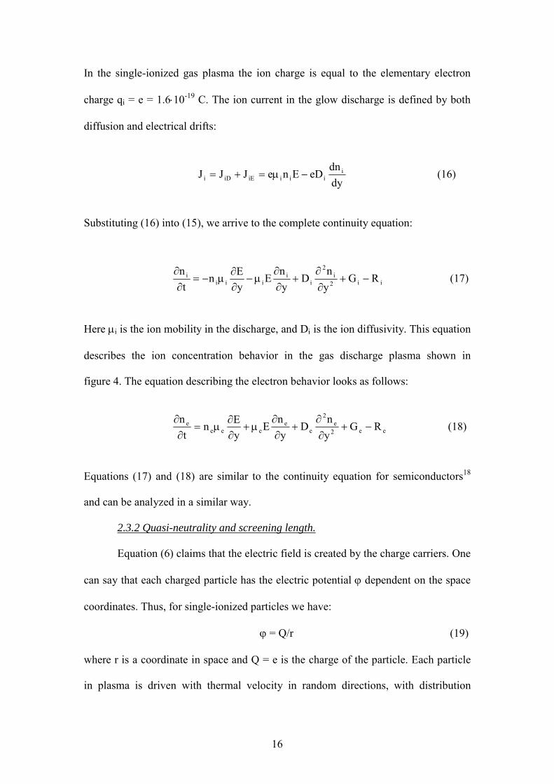
2.3.1 Continuity equation 14
2.3.2 Quasi-neutrality and screening length 16
2.3.3 Electrostatic plasma oscillation 18
2.3.4 Ambipolar diffusion 20
2.3.5 Charged carriers generation 21
2.3.6 Charged carriers recombination 24
2.3.7 External magnetic field influence 24
2.3.8 Sputtering in the plasma discharge 27
2.4 Triode sputtering application 31
2.4.1 Triode sputtering system implementation 31
2.4.2 External electromagnet 32
2.4.3 Internal parameters of the plasma 35
2.4.4 Practical Langmuir probe measurement 38
2.4.5 Thin film deposition by the plane discharge 46
2.5 Tetrode sputtering application 49
3. OPTIMIZATION AND IMPROVEMENT OF THE DEPOSITED FILMS 57
3.1 Mathematical modeling of the sputtering process with random
section method application 57

ix
3.1.1 Deposition of In2O3 conductive transparent coatings by DC
sputtering 61
3.1.1.1 Introduction 61
3.1.1.2 Experimental details 62
3.1.1.3 Practical model implementation 64
3.1.1.4 Experimental results 67
3.1.2 Deposition Ta resistive coatings with defined conductivity 74
3.1.2.1 Introduction 74
3.1.2.2 Experimental details 76
3.1.2.3 Practical model implementation 78
3.1.2.4 Experimental results 79
3.2 Vacuum Photothermal Processing (VPP) 85
3.2.1 Introduction 85
3.2.2 Development and investigation of VPP treatment 86
3.2.2.1 Basic Principles of Rapid Thermal Processing 86
3.2.2.2 Experimental details 88
3.2.2.3 Sample preparation 90
3.2.2.4 Control experiments 92
3.2.2.5 Experimental results 94
3.2.2.6 The mechanical properties of the films 98
3.2.2.7 The electrical properties of the films 104
3.2.3 VPP influence on the Schottky barrier height 108
4. CONCLUSIONS AND FUTURE DIRECTIONS 114
4.1 Conclusions 114
4.2 Future research direction 116
5. REFERENCES 117
x
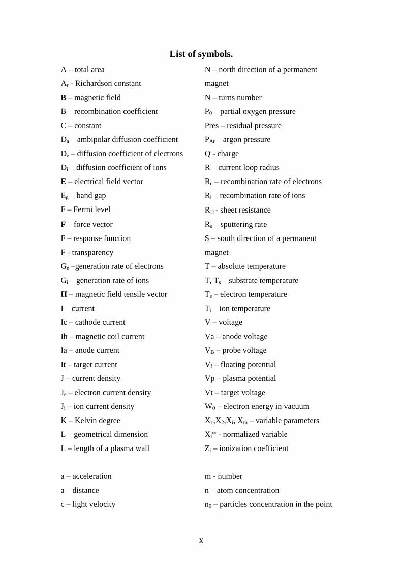
List of symbols. A – total area N – north direction of a permanent
Ar - Richardson constant magnet
B – magnetic field N – turns number
B – recombination coefficient P0 – partial oxygen pressure
C – constant Pres – residual pressure
Da – ambipolar diffusion coefficient PAr – argon pressure
De – diffusion coefficient of electrons Q - charge
Di – diffusion coefficient of ions R – current loop radius
E – electrical field vector Re – recombination rate of electrons
Eg – band gap Ri – recombination rate of ions
F – Fermi level R# - sheet resistance
F – force vector Rs – sputtering rate
F – response function S – south direction of a permanent
F - transparency magnet
Ge –generation rate of electrons T – absolute temperature
Gi – generation rate of ions T, Ts – substrate temperature
H – magnetic field tensile vector Te – electron temperature
I – current Ti – ion temperature
Ic – cathode current V – voltage
Ih – magnetic coil current Va – anode voltage
Ia – anode current VB – probe voltage
It – target current Vf – floating potential
J – current density Vp – plasma potential
Je – electron current density Vt – target voltage
Ji – ion current density W0 – electron energy in vacuum
K – Kelvin degree X1,X2,Xi, Xm – variable parameters
L – geometrical dimension Xi* - normalized variable
L – length of a plasma wall Zi – ionization coefficient
a – acceleration m - number
a – distance n – atom concentration
c – light velocity n0 – particles concentration in the point
xi
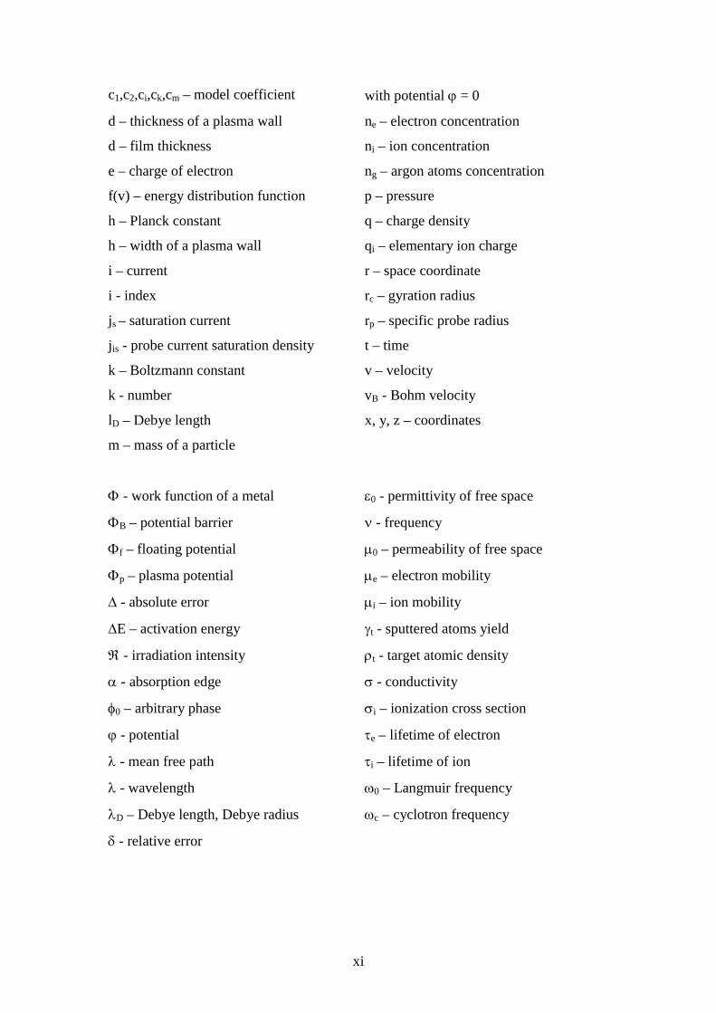
c1,c2,ci,ck,cm – model coefficient with potential ϕ = 0
d – thickness of a plasma wall ne – electron concentration
d – film thickness ni – ion concentration
e – charge of electron ng – argon atoms concentration
f(v) – energy distribution function p – pressure
h – Planck constant q – charge density
h – width of a plasma wall qi – elementary ion charge
i – current r – space coordinate
i - index rc – gyration radius
js – saturation current rp – specific probe radius
jis - probe current saturation density t – time
k – Boltzmann constant v – velocity
k - number vB - Bohm velocity
lD – Debye length x, y, z – coordinates
m – mass of a particle
Φ - work function of a metal ε0 - permittivity of free space
ΦB – potential barrier ν - frequency
Φf – floating potential µ0 – permeability of free space
Φp – plasma potential µe – electron mobility
∆ - absolute error µi – ion mobility
∆E – activation energy γt - sputtered atoms yield
ℜ - irradiation intensity ρt - target atomic density
α - absorption edge σ - conductivity
φ0 – arbitrary phase σi – ionization cross section
ϕ - potential τe – lifetime of electron
λ - mean free path τi – lifetime of ion
λ - wavelength ω0 – Langmuir frequency
λD – Debye length, Debye radius ωc – cyclotron frequency
δ - relative error
xii
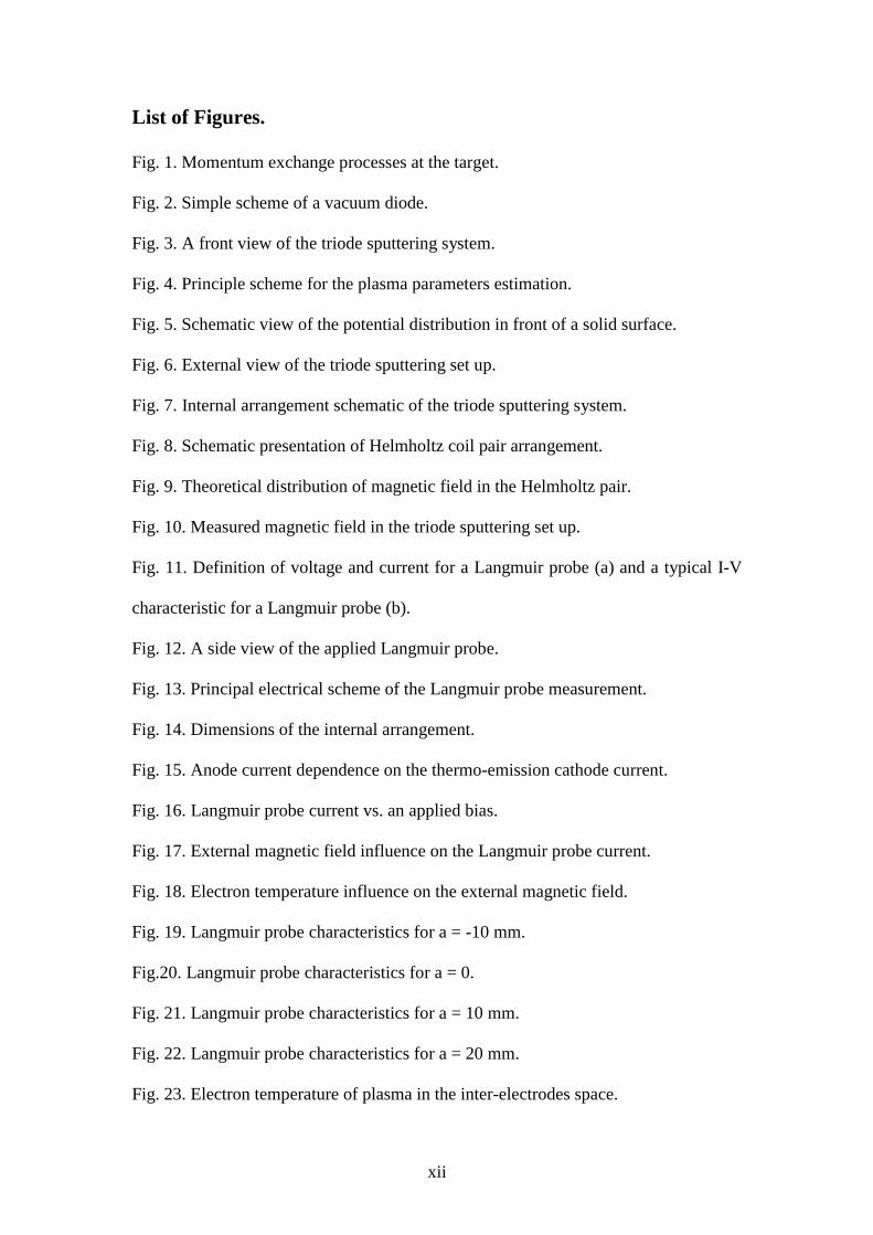
List of Figures.
Fig. 1. Momentum exchange processes at the target.
Fig. 2. Simple scheme of a vacuum diode.
Fig. 3. A front view of the triode sputtering system.
Fig. 4. Principle scheme for the plasma parameters estimation.
Fig. 5. Schematic view of the potential distribution in front of a solid surface.
Fig. 6. External view of the triode sputtering set up.
Fig. 7. Internal arrangement schematic of the triode sputtering system.
Fig. 8. Schematic presentation of Helmholtz coil pair arrangement.
Fig. 9. Theoretical distribution of magnetic field in the Helmholtz pair.
Fig. 10. Measured magnetic field in the triode sputtering set up.
Fig. 11. Definition of voltage and current for a Langmuir probe (a) and a typical I-V
characteristic for a Langmuir probe (b).
Fig. 12. A side view of the applied Langmuir probe.
Fig. 13. Principal electrical scheme of the Langmuir probe measurement.
Fig. 14. Dimensions of the internal arrangement.
Fig. 15. Anode current dependence on the thermo-emission cathode current.
Fig. 16. Langmuir probe current vs. an applied bias.
Fig. 17. External magnetic field influence on the Langmuir probe current.
Fig. 18. Electron temperature influence on the external magnetic field.
Fig. 19. Langmuir probe characteristics for a = -10 mm.
Fig.20. Langmuir probe characteristics for a = 0.
Fig. 21. Langmuir probe characteristics for a = 10 mm.
Fig. 22. Langmuir probe characteristics for a = 20 mm.
Fig. 23. Electron temperature of plasma in the inter-electrodes space.
xiii
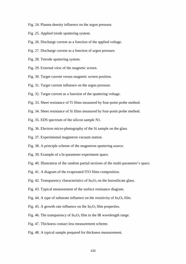
Fig. 24. Plasma density influence on the argon pressure.
Fig. 25. Applied triode sputtering system.
Fig. 26. Discharge current as a function of the applied voltage.
Fig. 27. Discharge current as a function of argon pressure.
Fig. 28. Tetrode sputtering system.
Fig. 29. External view of the magnetic screen.
Fig. 30. Target current versus magnetic screen position.
Fig. 31. Target current influence on the argon pressure.
Fig. 32. Target current as a function of the sputtering voltage.
Fig. 33. Sheet resistance of Ti films measured by four-point probe method.
Fig. 34. Sheet resistance of Si films measured by four-point probe method.
Fig. 35. EDS spectrum of the silicon sample N1.
Fig. 36. Electron micro-photography of the Si sample on the glass
Fig. 37. Experimental magnetron vacuum station.
Fig. 38. A principle scheme of the magnetron sputtering source.
Fig. 39. Example of a bi-parameter experiment space.
Fig. 40. Illustration of the random partial sections of the multi-parameter’s space.
Fig. 41. A diagram of the evaporated ITO films composition.
Fig. 42. Transparency characteristics of In2O3 on the borosilicate glass.
Fig. 43. Typical measurement of the surface resistance diagram.
Fig. 44. A type of substrate influence on the resistivity of In2O3 film.
Fig. 45. A growth rate influence on the In2O3 film properties.
Fig. 46. The transparency of In2O3 film in the IR wavelength range.
Fig. 47. Thickness contact less measurement scheme.
Fig. 48. A typical sample prepared for thickness measurement.
xiv
Fig. 49. Tantalum thin films photography (X 160): a–Ar pressure of 90 mTorr, b–Ar
pressure of 110 mTorr, c–Ar pressure of 130 mTorr, d–Ar pressure of 300 mTorr.
Fig. 50. Conductivity of tantalum films as a function of two variables: argon pressure
and sputtering voltage.
Fig. 51. Tantalum film conductivity at the calculated point.
Fig. 52. A 3-D presentation of the tantalum films conductivity as a function of the
technological parameters.
Fig. 53. Typical Rapid Thermal Annealing (RTA).
Fig. 54. Principle schematic of Vacuum Photothermal Processing set-up.
Fig. 55. Principle scheme of the I-V measurement.
Fig. 56. Typical MDSM structure for I-V characterization.
Fig. 57. Schematic upper and front view of the treated MSM samples.
Fig. 58. Typical Vacuum Photothermal Processing.
Fig. 59. Principle scheme of the VPP treatment set-up including a control electrode.
Fig. 60. Tungsten steams pressure.
Fig. 61. Tungsten coil temperature during VPP.
Fig. 62. Tungsten resistivity dependence on the temperature.
Fig. 63. Spectral efficiency of tungsten for different temperatures.
Fig. 64. Thermo-emission current density of Tungsten.
Fig. 65. Microscopic view of the Al-Al2O3-Ge-Au system (× 80).
Fig. 66. A 3D presentation of the Ge thin film surface (AFM microscope).
Fig. 67. External view of the processed MDSM samples.
Fig. 68. Experimental photographs of Ni electrodes on the silicon for as deposited and
VPP treated samples, in two magnifications: (a) as deposited film, *150; (b) as
deposited film, *3000; (c) VPP treated film, *150; (d) VPP treated film, *3000.

xv
Fig. 69. Experimental photographs of Ti electrodes on the silicon for as-deposited and
VPP treated samples for two different magnifications: (a) as deposited film, *150; (b)
as deposited film, *3000; (c) VPP treated film, *150; (d) VPP treated film, *3000.
Fig. 70. Samples temperatures vs. processing time for various thermal treatments.
Fig. 71. AFM 3D photographs of as deposited and VPP treated Ti films: (a) as
deposited Au-Si-Ti system; (b) VPP treated Au-Si-Ti system.
Fig. 72. AFM section analysis of the roughness for as-deposited and VPP treated Au-
Si-Ti systems: as deposited Au-Si-Ti system; (b) VPP treated Au-Si-Ti system.
Fig. 73. Electrical property measurements before and after a traditional furnace
annealing treatment of the glass-Al-Al2O3-Ge-Au system.
Fig. 74. VPP with glass filter (sample 1b).
Fig. 75. VPP processing of a glass-Al-Al2O3-Ge-Au system.
Fig. 76. Sheet resistance distribution of the glass-In2O3 system.
Fig. 77. Sheet resistance distribution of VPP processed glass-In2O3 system.
Fig. 78. I-V characterization of as deposited and VPP treated Au-Si-Au systems.
Fig. 79. I-V characterization of as deposited and VPP treated Au-Si-Ti systems with a
bias voltage in the control electrode.
Fig. 80. I-V characterization of as deposited and VPP treated Au-Si-Ni systems with a
bias voltage in the control electrode.
Fig. 81. The influence of a biased VPP treatment on the potential barrier magnitude in
Au-Si-Metal systems.
xvi
List of Tables.
Table 1. Typical sputtering parameters of the triode deposition system.
Table 2. Sputtering deposition rates using Argon (A°/min).
Table 3. Sputtering deposition parameters used for the Si films deposition.
Table 4. Different deposition process and its basic parameters.
Table 5. Standard form for the model coefficient estimation: F is the response
function and Xi* are the normalized process parameters.
Table 6. Normalized active technological parameters.
Table 7. Experimental data on the In2O3 film deposition.
Table 8. Optimized technological parameters.
Table 9. Parameters of the films after optimization.
Table 10.Variable deposition parameters of Ta films.
Table 11. Tantalum conductivity as a function of two variables.
Table 12. Parameters of the experimental trials.

1
1. INTRODUCTION
1.1 General
Over the past decades, thin-film science and technology have developed into a
major industry. This growth is a result of a fundamental understanding and
development of the processes and tools that are used in thin-film deposition. The
importance of coatings for the industry and the progress in synthesis of new materials
have produced an explosion of processing technologies1. There are many different
methods for thin-film deposition: chemical vapor deposition (CVD), plasma enhanced
chemical vapor deposition (PECVD), liquid reaction, condensation, and physical
vacuum deposition (PVD), including evaporation and sputtering which are
particularly important in thin-film deposition.
The main idea of these methods is separation of atoms from a substance and
deposition of these newly obtained atoms in the form of the required coating on a
substrate. We can regard the PVD process as consisting of three parts: 1) material
decomposition; 2) transportation of the separated material atoms to the substrate;
3) growing a thin film on the substrate. Each of these parts may be considered
separately. Each one is influenced by numerous technological parameters.
1. The first part of the process is defined by the energy introduced in the
decomposition process (for example, by heating the material in the vacuum
evaporation method). Such parameters as the residual vacuum level, presence of
reactive gas and pressure, or thermal properties of the material are only a few of
the many parameters that affect the first part of the process.
2. The space between the atom source and the substrate location, presence of plasma
in this space, and the level of vacuum are parameters that define the second part of
the process.
2
3. In the third part of the process, the focus is on the substrate and the processes
occurring in the vicinity of it in the vacuum chamber. Processes in the third part
are defined by such parameters as the energy of deposited atoms, the
contamination present on the surface of the substrate, and the substrate
temperature.
In this work, I aim to improve each part of the film growth process.
1.2 Sputtering Deposition Methods
Sputtering is one of the most effective methods of thin film deposition. It is
widely used in the present-day semiconductor2, photovoltaic3, and microelectronics4
industries. Materials with high melting points such as ceramics and refractory metals,
which are hard to deposit by evaporation, are easily deposited using sputtering.
Different sputtering methods, from a simple DC glow discharge sputtering to the
multi-electrode DC and RF sputtering, enable deposition of any type of material and
synthesis of new materials with pre-defined properties. For instance, sputtering can be
used to create a new metallic material from an intermetallic compound, this new
material having the same chemical composition as an intermetallic semiconductor
with a zinc-blend or wurtzit-type crystalline structure and being stable at the room
temperature and atmospheric pressure5. At the same time, each sputtering method has
its particular limitation (for example, DC sputtering requires a conductive target1, etc.)
Sputtering is a process in which highly energetic ions strike the surface of a
solid target, causing the emission of neutral atoms or molecules from the target
surface as a result of momentum transfer6. Assuming a hard-sphere elastic-collision
model7, the exchange of momentum among atoms in and around a collision cascade is
3
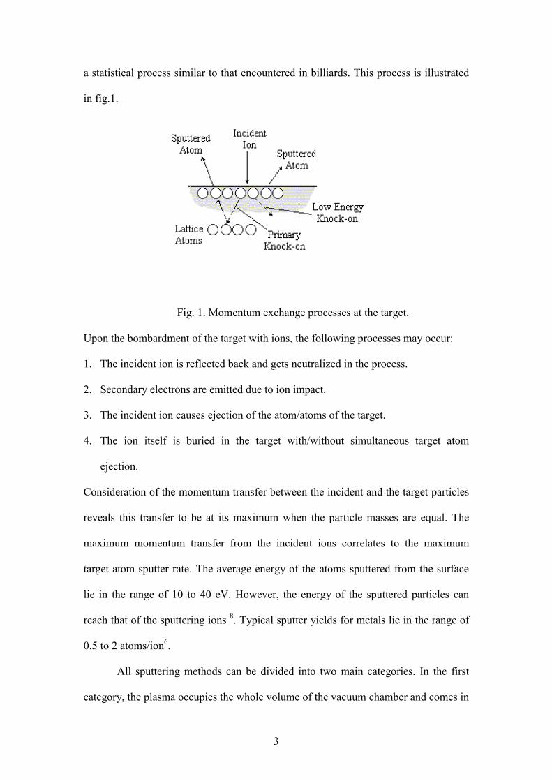
a statistical process similar to that encountered in billiards. This process is illustrated
in fig.1.
Fig. 1. Momentum exchange processes at the target.
Upon the bombardment of the target with ions, the following processes may occur:
1. The incident ion is reflected back and gets neutralized in the process.
2. Secondary electrons are emitted due to ion impact.
3. The incident ion causes ejection of the atom/atoms of the target.
4. The ion itself is buried in the target with/without simultaneous target atom
ejection.
Consideration of the momentum transfer between the incident and the target particles
reveals this transfer to be at its maximum when the particle masses are equal. The
maximum momentum transfer from the incident ions correlates to the maximum
target atom sputter rate. The average energy of the atoms sputtered from the surface
lie in the range of 10 to 40 eV. However, the energy of the sputtered particles can
reach that of the sputtering ions 8. Typical sputter yields for metals lie in the range of
0.5 to 2 atoms/ion6.
All sputtering methods can be divided into two main categories. In the first
category, the plasma occupies the whole volume of the vacuum chamber and comes in

4
contact with the grown layer and with the walls of a vacuum chamber. In the second
category, the plasma is confined to a restricted volume by means of electromagnetic
field or other method. In this case, independent control of different physical
parameters affecting the deposition process becomes especially important.
Each independent physical deposition parameter such as sputtering voltage,
substrate temperature or gas pressure, can be considered as a degree of freedom in the
deposition process. Controllability of the required coating properties increases with
the number of degrees of freedom. All known sputtering methods are based on a
number of variable input parameters that are independent and controllable. Up to now,
however, the distance between the plasma and the sputtering target has never been
used as an independent and controllable parameter. This novel parameter permits to
modify the film growth rate independently of all other deposition parameters.
The first part of this Thesis describes the mathematical modeling of plasma,
construction of a novel sputtering deposition system with several independent control
parameters and studying the processes in this system.
In order to develop a novel sputtering deposition process for a specific type of
film in the system with several independent parameters, a large number of
experiments are required. This number can be substantially reduced when using the
mathematical planning methods. A methodology for reducing the trial-and-errors
number is described in the second part of the Thesis.
A post-deposition treatment is also a very useful process for modifying and stabilizing
the film properties. Our novel post-deposition treatment method leads to an additional
level of freedom and to enhanced controllability. The innovative method for post-
deposition treatment called Vacuum Photo-thermal Processing (VPP) is described in
the third part of the Thesis.
5
2. PLANE GAS DISCHARGE APPLICATION FOR SPUTTERING
2.1 Introduction
Sputtering technology, which includes a large number of PVD methods, is
widely used for deposition of thin-film layers on semiconductor wafers. These layers
are used as diffusion barriers, primary conductors, antireflection coatings, etc. With
the progression toward finer topographical dimensions on wafers and increasing
aspect ratios, the broad angular distribution of sputtered atoms leads to poor coating
quality in deep grooves or other singularities on substrates9. This is mainly
conditioned by high energy of sputtered particles.
Sputter deposition is usually carried out in diode plasma systems known as
magnetrons. In these systems, the cathode is sputtered by ion bombardment and emits
atoms, which are then deposited on the wafer in the form of a thin film.
Originally, physical sputter deposition utilized DC diodes, which simply
represented parallel plates powered by a power supply of several kilovolts. This
process was conducted under the working pressure of several tens to hundreds of
mTorr. The negative plate, also known as the cathode or the sputtering target, was
bombarded with ions from the plasma volume set up between these two plates. The
sputtered cathode atoms could then deposit on various surfaces inside the vacuum
chamber, forming films. The DC diodes were characterized by slow deposition rates,
high voltage and low currents. This method was not suitable for deposition of
dielectric films.
Replacing the DC supply with an RF supply, usually operated at a frequency of
13.56 MHz, made deposition of dielectric films possible. However, the deposition
rates were no higher. A further improvement in sputtering techniques was achieved by
confining plasma electrons by means of magnetic field. This technique is known as
6
magnetron sputtering. Higher plasma density reduces the discharge impedance and
results in much higher current and lower voltage discharge. Another known sputtering
technique is the vacuum arc deposition process, which enables very high deposition
rates10.
The electron confinement in a magnetron is due to the presence of orthogonal
electrical (E) and magnetic (B) fields at the cathode surface. These fields result in a
classical E××××B drift for electrons (the Hall effect), which gives rise to a sequence of
cycloidal hopping steps parallel to the cathode face. As a result, the secondary
electrons, which are emitted from the cathode due to ion bombardment, are confined
to the nearest vicinity of the cathode. In a magnetron, the electric field is always
oriented normally to the cathode surface. The transverse magnetic field is configured
in such a way that the E××××B drift paths form closed loops, which trap the drifting
electrons and force them to circulate many times around the cathode face. As a
consequence, the ions sputter only a limited part of the cathode11 and create
heterogeneous etching ring zones on its surface.
In all of the above-mentioned sputtering methods, plasma occupies the entire
volume of the vacuum chamber and comes in contact with the internal metal parts and
the grown layer. Also, the self-sustained gas discharge in the diode system is mainly
supported by the auto-electron and secondary emission7. The voltage necessary to
initiate a discharge is defined by known framework of the Paschen law7, 110. After
initiating, the discharge current depend on the gas pressure and nearly independent of
the applied voltage (the normal glow discharge region111, 112). These conditions
negatively act on the quality of deposited coatings. A substrate charges negatively and
undergoes damage from plasma ions113. Also, this negative charge uncontrollably
changes conditions of the film growth.

7
Artificially supported sputtering methods can be divided into two basic
categories: in the first category, unconfined plasma contacts the substrate (so-called
ion-plating methods); in the second category, the plasma is confined by electro-
magnetic field, as seen in example [12]. If the plasma is in contact with the substrate
surface, its influence on the growing film gets out of control. This influence may
cause contamination in the deposited films, while uncontrolled heating of the growing
film may change its physical properties. An independent source of electrons, such as a
hot filament, is an important part of the artificial discharge system. It promotes a
significant decrease in the working pressure during sputtering and independently
controls the plasma current. In this case, the sputtering voltage (a high negative
voltage) is applied to the third electrode: the target to be sputtered. Therefore, this
system includes three electrodes with three independent supply sources: the cathode
heating supply, the plasma maintain supply (voltage applied to the anode-cathode
pair), and the high voltage sputtering supply (voltage applied to the sputtering target).
This system is called the triode sputtering system. Such a system was used for
deposition the signal electrodes for vidicons sensitive in the near UV spectrum13, 14.
As described in ref. [13, 14], the plasma was confined in the narrow flat band form by
a combination of collimating shield placed near the cathode and of an external
magnetic field. This magnetic field was produced by two identical electro-magnetic
coils placed at the distance equal to the coil radius (Helmholtz coils). This approach
enabled the formation of reproducible deposits of bi-layer thin-film systems of
Pd+Al2O3 with a transparency of 72% on the wavelength of 250 nm and resistivity no
more than 2 kOhm/sq. In these experiments, the Pd layers of the deposited films were
about 20 Å thick, and the alumina coating layers about 50 Å thick. The film
thickness was measured by a laser ellipsometer.
8
Since the considered discharge structure is highly non-uniform and very
complicated, a complete quantitative model of the discharge has not been developed.
It is of interest to estimate the parameters of plasma in the triode sputtering system.
These parameters are the plasma density, the electron temperature, and the floating
potential as a function of position of a point in a discharge gap.
2.2 Sputtering discharge modeling (qualitative description)
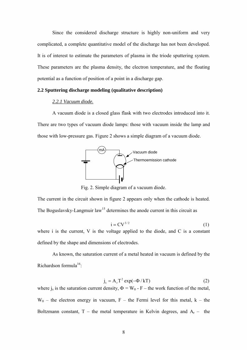
2.2.1 Vacuum diode.
A vacuum diode is a closed glass flask with two electrodes introduced into it.
There are two types of vacuum diode lamps: those with vacuum inside the lamp and
those with low-pressure gas. Figure 2 shows a simple diagram of a vacuum diode.
Fig. 2. Simple diagram of a vacuum diode.
The current in the circuit shown in figure 2 appears only when the cathode is heated.
The Boguslavsky-Langmuir law15 determines the anode current in this circuit as
where i is the current, V is the voltage applied to the diode, and C is a constant
defined by the shape and dimensions of electrodes.
As known, the saturation current of a metal heated in vacuum is defined by the
Richardson formula16:
where js is the saturation current density, Φ = W0 - F the work function of the metal,
W0 the electron energy in vacuum, F the Fermi level for this metal, k the
Boltzmann constant, T the metal temperature in Kelvin degrees, and Ar the
(1) CVi 2/3=
(2) )kT/exp(TAj 2rs Φ−=
mA Vacuum diode
Thermoemission cathode
9
Richardson constant equal to 120 A/cm2K2. This expression describes the current
density as a function of a heated metal temperature measured in Kelvin degrees. The
corresponding number of electrons emitted from the cathode surface can be simply
estimated from this current density.
A homogeneous magnetic field applied co-axially to the electrical field
(applied in the anode-cathode direction) confines the electrons emitted from thermo-
cathode. Thus, the greater part of the produced electrons will be collected on the
anode, while only a small part of them will recombine on the vacuum chamber walls
or return to the cathode. In this case, the current through the anode-cathode system
(diode) should increase. The maximum diode current is limited by the Richardson
expression. Note that the described case was collisionless.
2.2.2 Gas in the vacuum chamber.
Introducing gas in a vacuum chamber changes the picture due to additional
processes that may occur to gas atoms, such as collisions of various types, ionization,
etc. First of all, it is necessary to define the model which is best to apply here, i.e.,
vacuum, diffusion or intermediate model. As is known, gas particles moving inside a
bell jar collide. The average path between collisions, called the mean free path (λ), is
the critical parameter defining the type of model. If λ exceeds the geometrical
dimensions L of the vacuum chamber (λ>> L), one can use the vacuum (collisionless)
model, neglecting the diffusion processes in plasma. Practically, this case is described
by the relation λ > 4L. In the case when λ ≈ L, both vacuum and diffusion transfer
types should be considered. In the third case (λ < L), the transport properties of
plasma should be described using a diffusion model similar to the continuity equation
for semiconductors, although the case of gas requires a more complicated description.
A description using such a model (Schottky diffusion model for medium pressure)
10
appeared in a review by N. Braithwaite7. Complications here arise due to the presence
of non-homogeneous plasma and high rate of collisions between electrons, gas
molecules and ions.
Collisions may be of several types. For example, a collision of an electron
with an argon atom may excite the atom to a higher energy level without ionization:
e + Ar ⇒ Ar* + e (excitation), corresponding to the change of state 3p6 → 4p54s1 for
the valence electrons4. This metastable atom can then emit a photon and return to a
lower energy state e + Ar ⇒ Ar* + e ⇒ Ar + e + hν (relaxation process). The
radiation is usually in the visible or ultraviolet spectrum. Each gas is known to
possess an individual color at the plasma state. This color is explained by both
radiation processes: relaxation and recombination. Other processes are ionization acts
of the following types: e + Ar ⇒ Ar− or e + Ar ⇒ 2e + Ar+. The lifetime of these ions
is defined by the gas pressure, the applied voltage, and the applied magnetic field.
Each act of recombination is accompanied by an act of radiation.
The type of sputtering model to be applied can be determined by the critical
parameter, λ. Typical internal dimensions of vacuum stations in operation are ~ 30-50
cm. The working pressure p (Torr) appropriate for these dimensions (λ is measured in
cm) can be calculated from the known relation2:
p ≈ 5×10⁻³/λ (3)
If the gas pressure in the vacuum chamber is equal to ~1×10⁻³ Torr, we have the
boundary (intermediate) model. The diffusion processes can be neglected for the
pressure values of p ≤ 0.5×10⁻³ Torr (the ballistic transport model17). For the pressure
values higher than 1×10⁻³ Torr, only the diffusion transport model7, 17 can be used to
describe the processes of sputtering and deposition. It is important to distinguish
between two types of sputtered atom collisions: those with ions and those with neutral
gas molecules. Collisions between a sputtered atom and a gas ion may cause
11
ionization of the atoms and promote chemical reactions between the atoms and the
gas ions. Collisions between neutral gas atoms and a sputtered atom are called
thermalization. This term describes a cool-down of the sputtered atom energy to the
point where it matches the gas temperature (typically a few hundred degrees).
Obviously, the type and the amount of collisions define the film quality.
2.2.3 Triode sputtering system.
A triode sputtering discharge system is based using of a special electron
source. This source supports the sputtering process by emitting electrons throughout
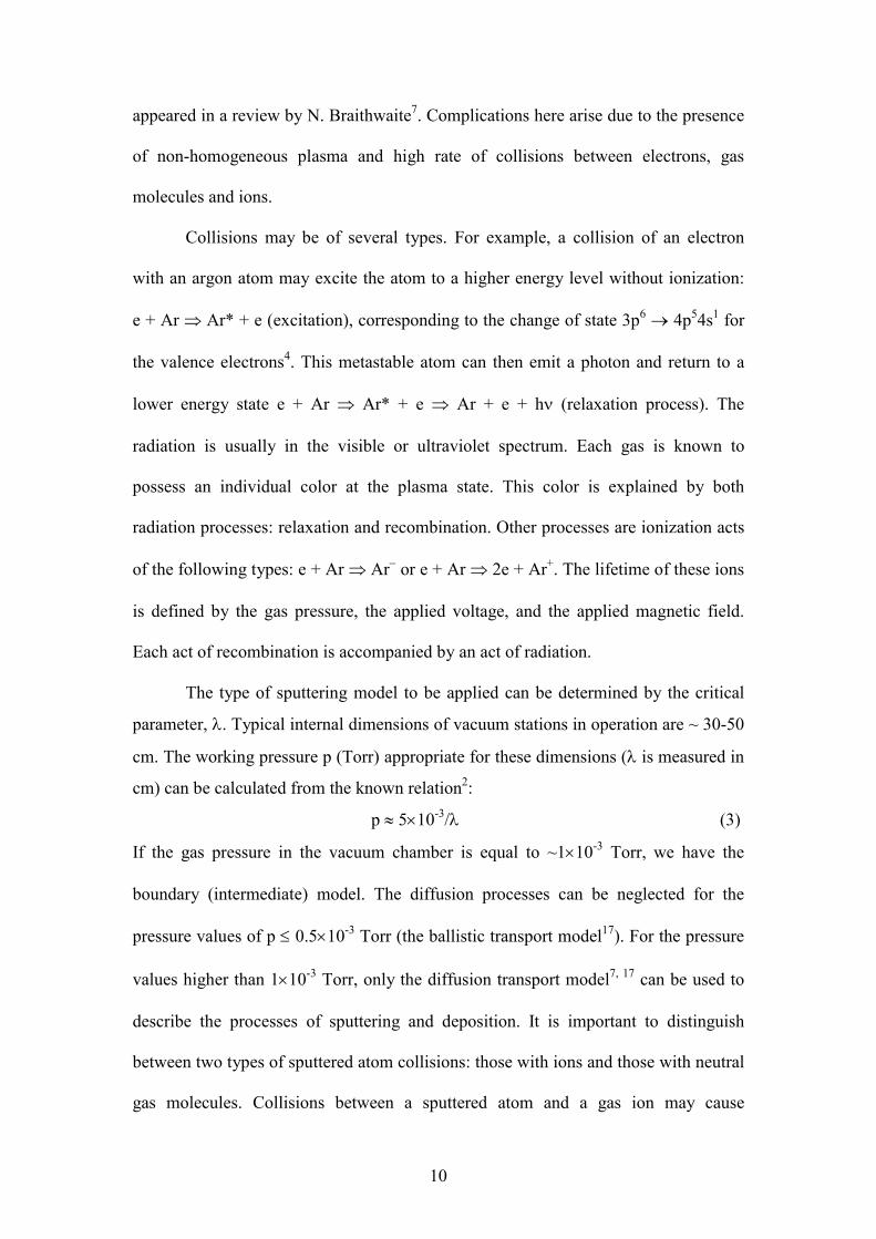
its duration. Figure 3 shows a diagram of a triode sputtering system13. This system
consists of a thermo-emissive cathode (the first electrode), a round anode, placed in
front of the cathode (the second electrode), and a water-cooled multiple target holder
connected to a high voltage supply (the third electrode). A metallic shield with a
collimating aperture in its center serves as the cathode screening. Externally mounted
electromagnet coils (Helmholtzs coils) generate a homogeneous magnetic field on
the electron beam axis. The substrate is located opposite the target, normally to the
anode-cathode axis; a rounded turning shield protects the substrate.
Fig. 3. A front view of the triode sputtering system.
12
The installation works as follows. The plasma-forming gas argon fills up a
bell jar after it has been evacuated up to residual vacuum. The argon pressure is set to
a required level defined by the sputtering conditions. The cathode current is switched
on to heat the tungsten coil. A constant electrical field is applied to the cathode-anode
gap to fire a forced discharge. The collimating aperture collimates this discharge to
the form of a band. The homogeneous magnetic field produced by the Helmholtz coils
confines the collimated discharge to a thin plasma band, to serve as the ion source in
the system. Confining of the plasma discharge increases the plasma current, therefore,
the ion concentration in the plasma band significantly increases. The plasma band
thickness is essentially less than the vacuum chamber dimensions. Therefore, we can
believe that the sputtered atoms overcome the targetsubstrate distance without
collisions with ions. Therefore, high ion concentration in the plasma band makes it
possible to decrease the gas pressure in the bell jar and thus transform the type of
sputtered atom transport from diffusion to intermediate or ballistic.
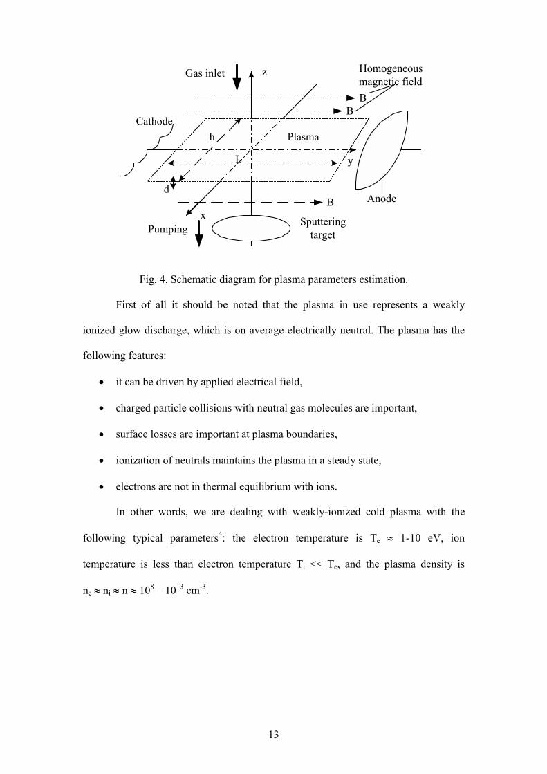
Let us now consider a model that can represent the triode sputtering process
described above and its physical parameters. Figure 3 represents a simplified scheme
of a triode sputtering system. The plasma in our case is a thin flat rectangle glow
volume. This volume consists of rarefied gas (argon), electrons and ions (mainly
positive single-ionized argon atoms). This volume occupies the space between the
cathode and the anode, as shown in figure 4, and is confined in the bell jar.
13
Fig. 4. Schematic diagram for plasma parameters estimation.
First of all it should be noted that the plasma in use represents a weakly
ionized glow discharge, which is on average electrically neutral. The plasma has the
following features:
• it can be driven by applied electrical field,
• charged particle collisions with neutral gas molecules are important,
• surface losses are important at plasma boundaries,
• ionization of neutrals maintains the plasma in a steady state,
• electrons are not in thermal equilibrium with ions.
In other words, we are dealing with weakly-ionized cold plasma with the
following typical parameters4: the electron temperature is Te ≈ 1-10 eV, ion
temperature is less than electron temperature Ti << Te, and the plasma density is
ne ≈ ni ≈ n ≈ 108 1013 cm-3.
x
y
z
Cathode
Anode
Plasma
L
h
d
BB
B
Homogeneousmagnetic field
Sputteringtarget
Gas inlet
Pumping

14
2.3 Plane plasma modeling (quantitative description)
2.3.1 Continuity equation.
The usual macroscopic form of Maxwells equations is30
where E and H are the electric and magnetic field vectors and µ0 = 4π⋅10-7 H/m and ε0
≈ 8.85⋅10-12 F/m are, respectively, the free space permeability and permittivity. The
sources of the electrical and the magnetic fields are, respectively, the charge density q
and the current density J. The charge density change in a point can be obtained by
taking a partial time derivative of Equation (6) and substituting the expression for the
magnetic field source from Equation (5).
According to the known formula of the vector analysis,
∇∇∇∇(∇∇∇∇××××H) = 0 (10)
Substituting Equations (8) and (10) into (9), we get the charge continuity equation in
the form of the charge conservation law:
====⋅⋅⋅⋅∇∇∇∇
====⋅⋅⋅⋅∇∇∇∇
++++====××××∇∇∇∇
−−−−====××××∇∇∇∇
) (H
) (E
)(JEH
) (HE
7 0
6 q
5 t
4 t
0
0
0
ε
∂∂
ε
∂∂
µ
(((( )))) )8(tq
t 0 E ∂∂
ε∂∂
====∇∇∇∇
(((( )))) (((( )))) (((( )))) (9) tt 00 JHJHEE ∇∇∇∇−−−−××××∇∇∇∇∇∇∇∇====−−−−××××∇∇∇∇∇∇∇∇====
∇∇∇∇====∇∇∇∇
∂∂
εε∂∂
)11(0tq +J ====∇∇∇∇
∂∂

15
The charge density q may be appeared as a sum q = niqi - nee of ion and electron
components. Taking into account this assumption in the weakly-ionized plasma, the
equation (11) can be written independently for each type of charged carriers.
Therefore, we can write these equations in a one-dimensional form as follows:
for electrons and
for ions. Here A⋅dy = d⋅h⋅dy is an elementary volume of a plasma slice with cross-
section area A and thickness dy; ni and ne concentrations of the ions and electrons in
the slice; e and qi are elementary charges of electron and ion; Ji and Je ion and
electron current densities in the corresponding part of the slice; Gi and Ge generation
rates of ions and electrons in the slice; and Ri and Re decreasing rates of the ion and
electron amounts in the slice.
If we assume that the ion current in the Y-direction changes continuously (at least in
the positive column region), we can write
Now equation (13) transforms to the following equation:
(14) dyyJ
)yy(J)y(J iii
∂∂
−=δ+−
(15) RGyJ
q1
tn
iii
i
i −+∂∂
−=∂
∂
( ) ( )[ ] (12) dyRAdyGAyyJyJeAdyA
tn
eeeee ⋅−⋅+δ+−−=⋅
∂∂
( ) ( )[ ] (13) dyRAdyGAyyJyJqAdyA
tn
iiiii
i ⋅−⋅+δ+−=⋅∂
∂
16
In the single-ionized gas plasma the ion charge is equal to the elementary electron
charge qi = e = 1.6⋅10-19 C. The ion current in the glow discharge is defined by both
diffusion and electrical drifts:
Substituting (16) into (15), we arrive to the complete continuity equation:
Here µi is the ion mobility in the discharge, and Di is the ion diffusivity. This equation
describes the ion concentration behavior in the gas discharge plasma shown in
figure 4. The equation describing the electron behavior looks as follows:
Equations (17) and (18) are similar to the continuity equation for semiconductors18
and can be analyzed in a similar way.
2.3.2 Quasi-neutrality and screening length.
Equation (6) claims that the electric field is created by the charge carriers. One
can say that each charged particle has the electric potential ϕ dependent on the space
coordinates. Thus, for single-ionized particles we have:
ϕ = Q/r (19)
where r is a coordinate in space and Q = e is the charge of the particle. Each particle
in plasma is driven with thermal velocity in random directions, with distribution
(16) dydn
eDEneJJJ iiiiiEiDi −µ=+=
(17) RGyn
Dyn
EyEn
tn
ii2i
2
ii
iiii −+
∂∂
+∂∂
µ−∂∂
µ−=∂
∂
(18) RGyn
Dyn
EyEn
tn
ee2e
2
ee
eeee −+
∂∂
+∂∂
µ+∂∂
µ=∂
∂

17
subject to Boltzmann rule. The electrical field E is equal to the potential gradient and
acts in the opposite direction:
E = -∇∇∇∇ ϕ (20)
Substituting (20) into (6) yields the well-known Poisson equation:
where q is the charge density dependent on the space coordinates. Taking into
account the Boltzmann distribution
where T is the temperature, n is the concentration of charged particles in the point
with the potential of ϕ, and n0 is the concentration of charged particles in the point
with ϕ = 0, i.e., the average concentration of particles over the entire space. The
Poisson equation can be written in the form:
To solve this equation, we simplify it, assuming the random deviations of the
momentary concentrations and potential fluctuation. Based on this assumption, we
can develop the exponential function in a Taylor series and stop after the second
term20, thus linearizing the right side in Equation (24):
(21) q∆000 ====−−−−====−−−−∇∇∇∇∇∇∇∇====∇∇∇∇ ϕεϕεε )(E
(22) q
0ε−=ϕ∆
(23) enn kTe
0
ϕ−
=
(24) ene kTe
00
ϕ−
ε−=ϕ∆
(25) kTen
0
20 ϕ
ε−=ϕ∆
18
For a spherical symmetrical distribution of potential near the charged particle
(charged point), we obtain the solution in the form of:
where C is an integration constant that approximates to e (see Prediction (19)), and lD
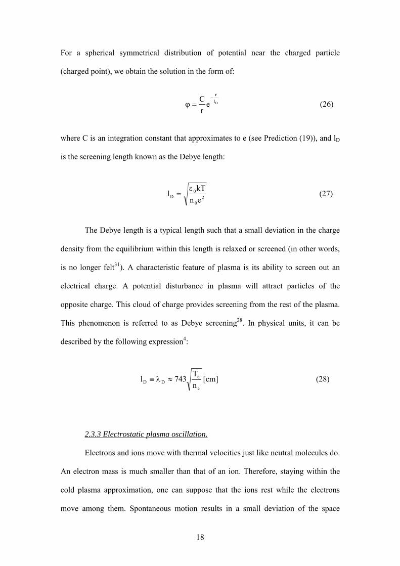
is the screening length known as the Debye length:
The Debye length is a typical length such that a small deviation in the charge
density from the equilibrium within this length is relaxed or screened (in other words,
is no longer felt31). A characteristic feature of plasma is its ability to screen out an
electrical charge. A potential disturbance in plasma will attract particles of the
opposite charge. This cloud of charge provides screening from the rest of the plasma.
This phenomenon is referred to as Debye screening28. In physical units, it can be
described by the following expression4:
2.3.3 Electrostatic plasma oscillation.
Electrons and ions move with thermal velocities just like neutral molecules do.
An electron mass is much smaller than that of an ion. Therefore, staying within the
cold plasma approximation, one can suppose that the ions rest while the electrons
move among them. Spontaneous motion results in a small deviation of the space
(26) erC
Dlr
−
=ϕ
(27) enkT
l 20
0D
ε=
(28) [cm] nT
743le
eDD ≈λ≡
19
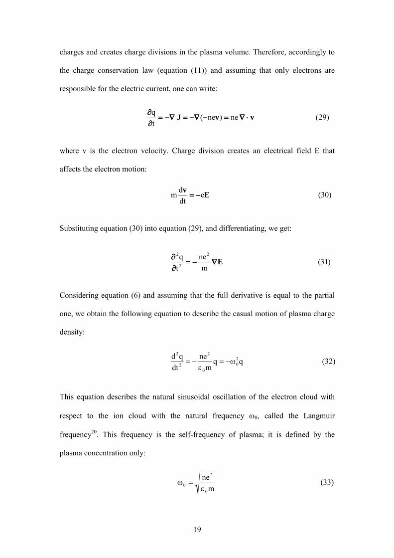
charges and creates charge divisions in the plasma volume. Therefore, accordingly to
the charge conservation law (equation (11)) and assuming that only electrons are
responsible for the electric current, one can write:
where v is the electron velocity. Charge division creates an electrical field E that
affects the electron motion:
Substituting equation (30) into equation (29), and differentiating, we get:
Considering equation (6) and assuming that the full derivative is equal to the partial
one, we obtain the following equation to describe the casual motion of plasma charge
density:
This equation describes the natural sinusoidal oscillation of the electron cloud with
respect to the ion cloud with the natural frequency ω0, called the Langmuir
frequency20. This frequency is the self-frequency of plasma; it is defined by the
plasma concentration only:
)29 (ne)ne(tq v vJ ⋅⋅⋅⋅∇∇∇∇====−−−−−−−−∇∇∇∇====−−−−∇∇∇∇====
∂∂∂∂∂∂∂∂
)30(edtdm Ev
−−−−====
)31 (m
netq 2
2
2
E∇∇∇∇−−−−====∂∂∂∂∂∂∂∂
(32) qqm
nedt
qd 20
0
2
2
2
ω−=ε
−=
(33) m
ne
0
2
0 ε=ω
20
2.3.4 Ambipolar diffusion.
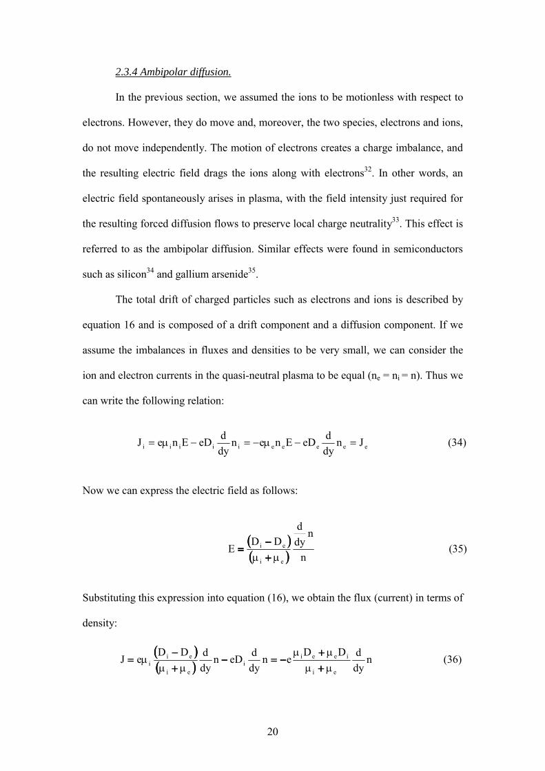
In the previous section, we assumed the ions to be motionless with respect to
electrons. However, they do move and, moreover, the two species, electrons and ions,
do not move independently. The motion of electrons creates a charge imbalance, and
the resulting electric field drags the ions along with electrons32. In other words, an
electric field spontaneously arises in plasma, with the field intensity just required for
the resulting forced diffusion flows to preserve local charge neutrality33. This effect is
referred to as the ambipolar diffusion. Similar effects were found in semiconductors
such as silicon34 and gallium arsenide35.
The total drift of charged particles such as electrons and ions is described by
equation 16 and is composed of a drift component and a diffusion component. If we
assume the imbalances in fluxes and densities to be very small, we can consider the
ion and electron currents in the quasi-neutral plasma to be equal (ne = ni = n). Thus we
can write the following relation:
Now we can express the electric field as follows:
Substituting this expression into equation (16), we obtain the flux (current) in terms of
density:
(34) JndydeDEnen
dydeDEneJ eeeeeiiiii =−µ−=−µ=
(((( ))))(((( )))) )35 (
n
ndyd
DDE
ei
ei µµ ++++
−−−−====
(((( ))))(((( )))) )36 (n
dydDD
endydeDn
dydDD
eJei
ieeii
ei
eii
µµµµ
µµµ
++++++++
−−−−====−−−−++++−−−−
====
21
Now we can rewrite the expression (36), with the term Da as an ambipolar diffusion
coefficient:
Here the ambipolar diffusion coefficient is equal to
Since the electron mobility is much greater than that of ions, we can simplify the form
of Da as:
Taking in account the known Einstein relation36:
we get:
From (41) we see that the ambipolar diffusion is controlled by the slower particles (in
our case the ions), but increases in direct proportion to the temperature ratio. Thus, if
Te >> Ti, which is the usual case in weakly ionized plasma, the diffusion rates of both
ions and electrons are much higher than that of free ions.
2.3.5 Charged carriers generation.
Ionization of neutral particles (argon atoms) in the case of not self-sustained
discharge is normally achieved by electron impact. The electrons are produced by
(37) dyneDJ a
∂=
(38) DD
Dei
ieeia µ+µ
µ+µ=
(39) DDD ee
iia µ
µ+=
(41) TT
1DDi
eia
+=
(40) e
kTD µ=

22
thermo-electron emission from a hot filament (tungsten) and accelerated to about 100
eV. This energy is sufficient to ionize argon atoms, whose ionization potential is
equal to 15.76 eV23. The energy of thermally produced electrons is not
monochromatic, but rather has a Boltzmann distribution37. The amount of collisions
between the electrons and other particles in the plasma is defined by the argon
pressure. A detailed consideration of all collision types: ionization, excitation, and
recombination processes in the plasma is very complicated and practically
impossible19. Moreover, all processes in plasma are probabilistic, so that a precise
solution of a system describing the behavior of each particle is useless20.
A solid surface in contact with plasma will charge up negatively with respect
to the plasma. The reason for this is the mass difference between the electrons and the
ions. The main part of the potential difference between the solid and the plasma will
be confined to a narrow sheath restricted to several Debye lengths in thickness28. This
potential distribution is schematically shown in figure 5.
Fig. 5. Schematic view of the potential distribution in front of a solid surface.
Electrons emitted by the hot cathode run through the sheath distance and begin
to move through the plasma volume. Initially there are no electrons in the volume, and
23
we can write the first condition for the electrons movement as a function of two
variables, the distance y (see fig. 4) and the time t:
n(y,t) = n0(y,0) = 0 (42)
In the course of time, an area with high electron concentration arises at the border of
the plasma volume. This surface concentration is constant and equal to the amount of
emitted electrons (see formula (2)). Electrons move through the plasma volume in
accordance with the Fick law. On their way, however, the electrons collide with the
neutral argon atoms, and the number of electrons decreases. One can say that this
diffusion process never takes electrons through the entire depth of the plasma volume.
In other words, if we assume that the plasma volume is infinite, we can write:
nt(∞,t) = 0 (43)
Taking into account conditions (42) and (43), we obtain that the electron movement in
the case of the forced (non-self-sustained) discharge can be described as diffusion
from a constant source, i.e., in terms of the error function38.
This type of electron behavior lasts for a limited time period, until a sufficient amount
of positive ions is generated.
A typical degree of ionization in the weakly ionized plasma does not exceed 1 atom in
104 items; therefore most of argon atoms remain neutral21. These neutral atoms have
the thermal energy corresponding to the ambient temperature and thus play a minor
role in the process. The ion generation rate can be presented in the form22:
Gi = Zine (45)
where Zi is the ionization coefficient and ne is the number of emitted electrons. Here
the electron concentration ne is defined by the Richardson formula16 and is equal to
(44) Dt2
yerfcn)t,y(n 0
=

24
8.2⋅1015 electrons · cm-2s-1 for the cathode temperature 2000 K 7. The ionization
coefficient Zi is defined by the pressure in the vacuum chamber, the electron energy
distribution, the electron velocity, and the cross-section of the argon atoms7:
where f(v) is the energy distribution function for electrons, ng the argon
concentration, σi the ionization cross-section, and f(v)dv the weighting. The
integration in the numerator does the adding, while the denominator completes the
weighting averaging.
2.3.6 Recombination of charged carriers.
Parameters Ri and Re in the continuity equations (17) and (18) describe the
recombination rate of the charged carriers. The processes of recombination are caused
by collisions between electrons and ions7. The amount of collisions is determined by
the argon concentration in the vacuum chamber and the argon cross-section, that is,
by the time between atom collisions, or lifetime:
where τi and τe are lifetimes of ions and electrons and B is a recombination
coefficient, which depends on the collision cross-section and the energy distribution
of the interacting particles.
2.3.7 External magnetic field influence.
Every charge is a source of the electric field, through which it exerts force on
any other charge in inverse square proportion to the distance between them. An
(46) dv)v(f
dv)v(vf)v(nZ
0
0 ig
i
∫∫
∞
∞σ
=
(47) n
Bn/1n
Bn/1nn
RRe
e
g
e
g
i
i
iie τ
===τ
≈≈
25
electric field imposed externally will apply forces to any charge that enters it. Charges
that move with respect to magnetic fields also experience forces. The Lorentz force
conveniently combines the electric and magnetic effects on a charge7:
F = e(E + v××××B) (48)
Here e is the elementary charge in Coulombs; E is the electric field in Volts per
meter; v is the velocity in meter per second; ×××× implies the vector product; and B is the
magnetic flux density in Teslas. In the case of constant electric field E = E0 without
magnetic field (B ≡ 0), a particle moves with a constant acceleration along E0 (see
figure 4):
y(t) = y0 + v0t + 0.5a0t2 (49)
where y0 and v0 are the particle position and velocity at t = 0 and a0 = eE0/m.
For the negative particles and a constant magnetic field B = B0, which we take
to lie along y, with E ≡ 0, the components of (48) are:
A motion of charge in the direction y is coupled from the x and z motions.
Differentiating (51) and eliminating vx with the help of (50), we obtain
This equation describes the circular motion of a charged particle with gyration
(cyclotron) frequency equal to:
=
=
−=
(52) 0dt
dvm
(51) dt
dvm
(50)
y
0z
0
Bev
Bevdt
dvm
x
zx
(53) vm
)eB(dt
vdz2
20
2z
2
−=
26
Solving Equation (53) and using (54) to obtain vx, we have:
where v⊥0 is the speed component perpendicular to B0 (y-axis), and φ0 is an arbitrary
phase. Integrating yields the particle position
where
is the gyration radius, which can be expressed through the particle energy15:
Equations (58) - (60) show that the particle moves in a circular orbit perpendicular to
B, with frequency ωc and radius rc, around a guiding center with coordinates
(x0,z0,y0+vy0t), which moves uniformly along y. Positive ions gyrate around the
(54) m
eB0c =ω
=
φ+ω−=
φ+ω=
⊥
⊥
(57) vv
(56) )t(Sinvv
(55) )t(Cosvv
0yy
0c0x
0c0z
+=
φ−+φ+ω=
φ−+φ+ω=
(60) tvyy
(59) )Cosrx()(Cosr x
(58) )Sinrz()(Sinrz
0y0
0c00cc
0c00cc
(61) v
rc
0c ω
= ⊥
(62) B
)kT(em2r
0
5.05.0
=

27
magnetic field lines according to the left-hand rule, and electrons gyrate according to
the right-hand rule.
The non-self-sustained discharge applied in the system on figure 4 uses both
constant electric and constant magnetic fields. The directions of both fields are
parallel to each other. Thus, the field components can be written as follows:
Bx = Bz = 0; By = B0; Ex = Ez = 0; Ey = E0 (63)
Expressing v as a vector sum v = vy(t) + v⊥(t) in the Lorentz force equation (48), we
obtain the uniform acceleration along y and an equation for the transverse motion:
Solving this equation in a general form is a rather complicated task. However, we can
consider a combined solution of (49) and (58) - (60).
All the particles that move along y-axis are not affected by the deviated forces such as
E0 ×××× B0 ≡ 0 (65)
Electrons and ions that have a perpendicular velocity component obtain gyration
influence, which increases with the angle between the velocity and the y-axis. In other
words, the constant magnetic field that is parallel to the applied electric field confines
the charged particles in the plasma. Thus, a flat plasma band can be obtained on the
following conditions: applying a hot cathode electron source, using a collimating
aperture, and applying an external magnetic field directed in parallel to the applied
electric field.
2.3.8 Sputtering in the plane discharge.
A sputtering process begins with supplying a high negative voltage to the
target. This process, as shown above, consists in the ion bombardment of the
(64) 0Bevdt
dvm ×= ⊥⊥
28
sputtering target. Therefore, a part of the ions leave the positive plasma column. The
sputtering process in a system with plane forced discharge occurs in the direction (z-
axis) perpendicular to the anode-cathode axis (see figure 4). We can write the
equations describing the ion collection process and the sputtering process for this
direction. The concentration of ions in the plasma band is homogeneous in the y and
x-directions since it is defined by the Helmholtz coil pair26. The ions formed by the
discharge in the triode sputtering system are collected by the entire target surface.
This is a very important advantage of the described sputtering process in comparison
with the magnetron sputtering, in which sputtering is not homogeneous11. Also, the
sputtered particles in the magnetron sputtering were shown to be ionized27, which is
excluded with the triode sputtering.
The floating potential of the positive column, which usually amounts to
several tens volts, does not enable any particles to be sputtered from the target
surface. The commonly used sputtering voltage ranges from 500 to 3,000 V, which
makes it possible to neglect the value of floating potential during sputtering. One can
consider (with idealization) the plane discharge and the surface of sputtering target as
two infinite plane-parallel plates, similar to a plane-parallel capacitor. One of the
plane-parallel plates emits charged particles (ions) and has the potential equal to that
of the plasma. The other plate has the sputtering potential Vt (the target potential) and,
in the first approximation, perfectly absorbs all the arriving charged particles. Let us
assume that the plasma plate emits only one type of particles, with charge +q and
mass mi, at zero velocity. The sheath edge formed by the discharge is defined as a
position where the ions reach the ion sound speed. The potential in the described
capacitor is given by the Poisson equation, which we can write, for the sake of
simplicity, in the one-dimensional form:
29
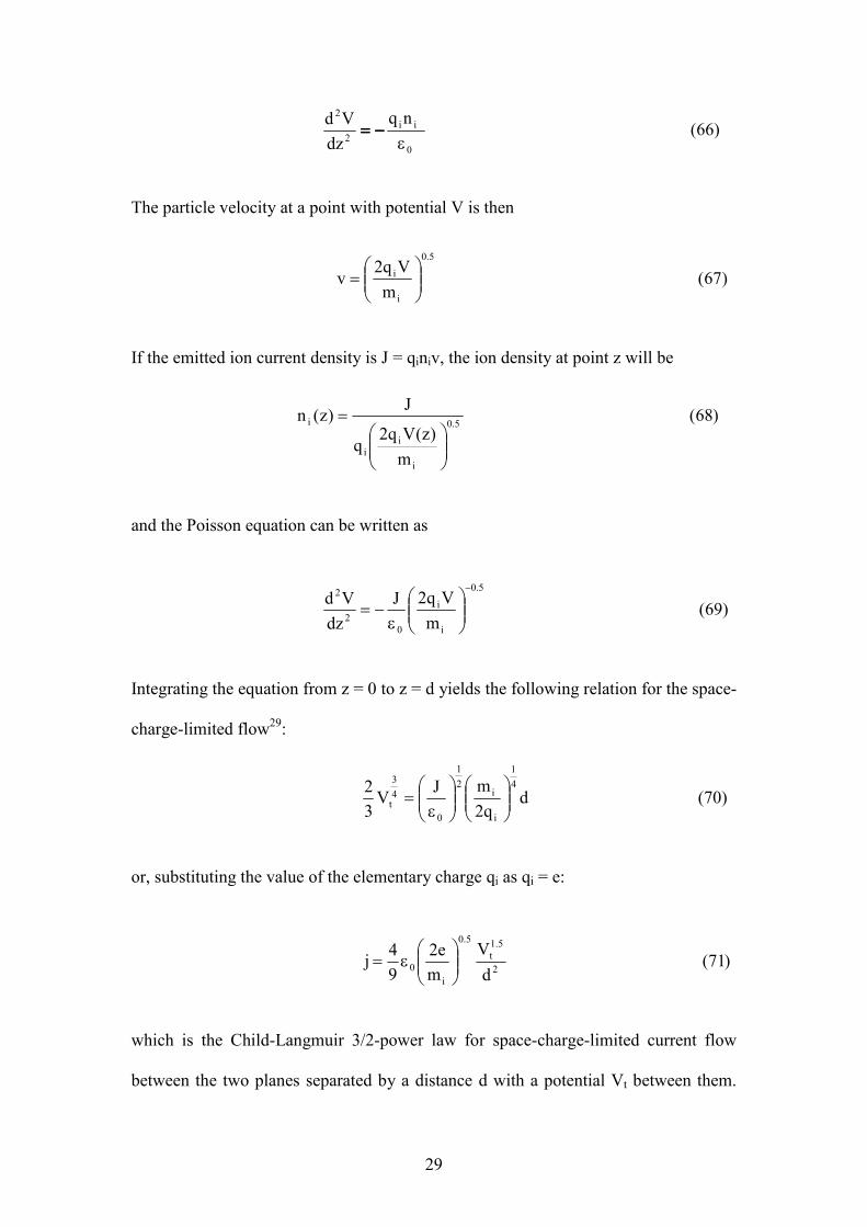
The particle velocity at a point with potential V is then
If the emitted ion current density is J = qiniv, the ion density at point z will be
and the Poisson equation can be written as
Integrating the equation from z = 0 to z = d yields the following relation for the space-
charge-limited flow29:
or, substituting the value of the elementary charge qi as qi = e:
which is the Child-Langmuir 3/2-power law for space-charge-limited current flow
between the two planes separated by a distance d with a potential Vt between them.
)66(nq
dzVd
0
ii2
2
ε
−−−−====
)67 (m
Vq2v
5.0
i
i
=
)68(
m)z(Vq2
q
J)z(n 5.0
i
ii
i
=
)69(m
Vq2Jdz
Vd5.0
i
i
02
2
−
ε
−=
)70(dq2
mJV32 4
1
i
i21
0
43
t
ε
=
)71(d
Vm
e294j 2
5.1t
5.0
i0
ε=

30
The current density obtained in the formula (71) is the target ion current. This current
can be measured during sputtering only.
Now let γt be the yield of sputtered atoms per incident ion and ρt the atomic
density of the sputtering target material. Then the sputtering rate can be written as:
(72) [cm/s] 1ejR
t
its ρ
γ=
31
2.4 Triode sputtering application
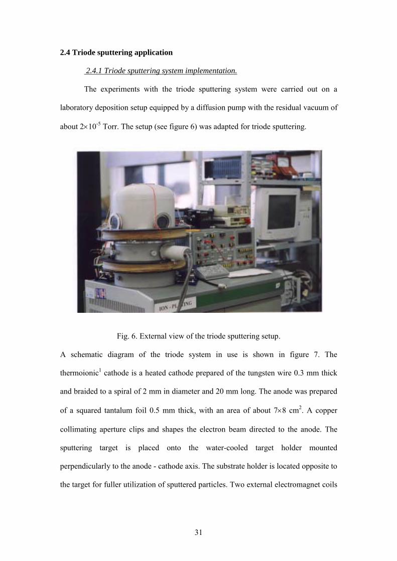
2.4.1 Triode sputtering system implementation.
The experiments with the triode sputtering system were carried out on a
laboratory deposition setup equipped by a diffusion pump with the residual vacuum of
about 2×10⁻⁵ Torr. The setup (see figure 6) was adapted for triode sputtering.
Fig. 6. External view of the triode sputtering setup.
A schematic diagram of the triode system in use is shown in figure 7. The
thermoionic1 cathode is a heated cathode prepared of the tungsten wire 0.3 mm thick
and braided to a spiral of 2 mm in diameter and 20 mm long. The anode was prepared
of a squared tantalum foil 0.5 mm thick, with an area of about 7×8 cm2. A copper
collimating aperture clips and shapes the electron beam directed to the anode. The
sputtering target is placed onto the water-cooled target holder mounted
perpendicularly to the anode - cathode axis. The substrate holder is located opposite to
the target for fuller utilization of sputtered particles. Two external electromagnet coils
32
of 34 cm in diameter arranged co-axially with the anode - cathode axis were used to
create a homogeneous magnetic field in the discharge space.
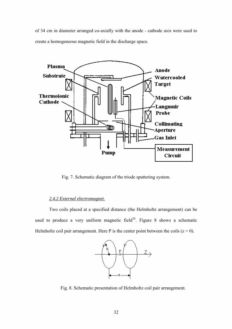
Fig. 7. Schematic diagram of the triode sputtering system.
2.4.2 External electromagnet.
Two coils placed at a specified distance (the Helmholtz arrangement) can be
used to produce a very uniform magnetic field26. Figure 8 shows a schematic
Helmholtz coil pair arrangement. Here P is the center point between the coils (z = 0).
Fig. 8. Schematic presentation of Helmholtz coil pair arrangement.
33
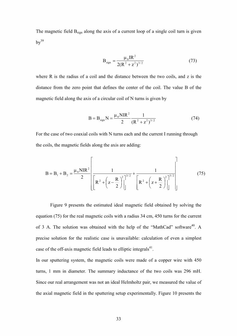
The magnetic field Bsign along the axis of a current loop of a single coil turn is given
by39
where R is the radius of a coil and the distance between the two coils, and z is the
distance from the zero point that defines the center of the coil. The value B of the
magnetic field along the axis of a circular coil of N turns is given by
For the case of two coaxial coils with N turns each and the current I running through
the coils, the magnetic fields along the axis are adding:
Figure 9 presents the estimated ideal magnetic field obtained by solving the
equation (75) for the real magnetic coils with a radius 34 cm, 450 turns for the current
of 3 A. The solution was obtained with the help of the MathCad software40. A
precise solution for the realistic case is unavailable: calculation of even a simplest
case of the off-axis magnetic field leads to elliptic integrals41.
In our sputtering system, the magnetic coils were made of a copper wire with 450
turns, 1 mm in diameter. The summary inductance of the two coils was 296 mH.
Since our real arrangement was not an ideal Helmholtz pair, we measured the value of
the axial magnetic field in the sputtering setup experimentally. Figure 10 presents the
(74) )zR(
12
NIRNBB 2/322
20
sign +µ
==
(75)
2RzR
1
2RzR
12
NIRBBB 2/32
2
2/322
20
21
++
+
−+
µ=+=
(73) )zR(2
IRB 2/322
20
sign +µ
=

34
experimentally measured magnetic field values. The magnetic field was measured
using the Digital Teslameter DTM-132 of Group 3. The current running through the
coils was 3 A.
Fig. 9. Theoretical distribution of magnetic field in the Helmholtz pair.
-2 0 2 4 6 8 10 12 14 16 180
102030405060708090
100110120130140150160170180190
Internal field between coils (z = 0) Edge field of the coil (z = 5 cm) Magnetic field outside of the coil (z = 8 cm) Magnetic field outside of the coil (z = 11 cm)
Axia
l mag
netic
fiel
d, G
s
Distance from the coil center, cm
Fig. 10. Measured magnetic field in the triode sputtering setup.
35
2.4.3 Internal plasma parameters.
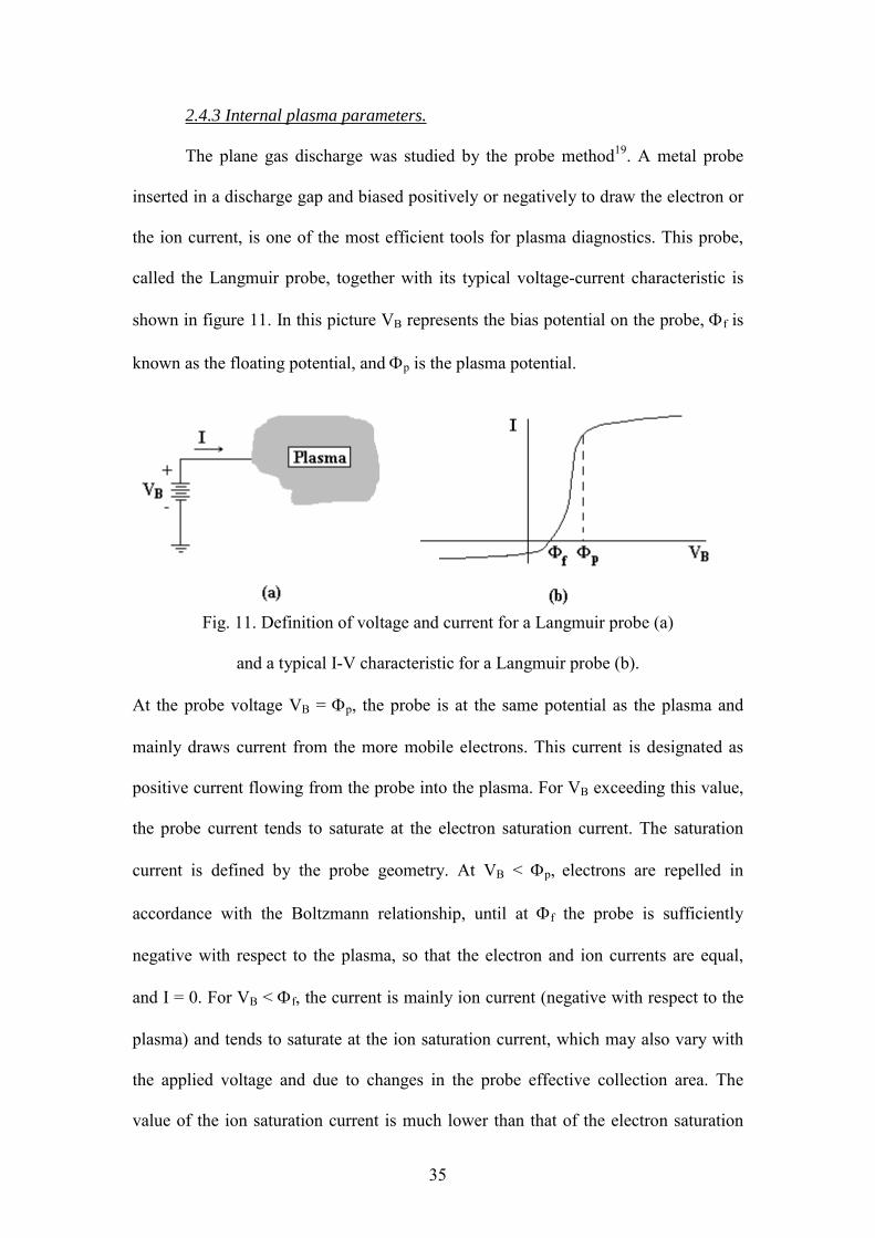
The plane gas discharge was studied by the probe method19. A metal probe
inserted in a discharge gap and biased positively or negatively to draw the electron or
the ion current, is one of the most efficient tools for plasma diagnostics. This probe,
called the Langmuir probe, together with its typical voltage-current characteristic is
shown in figure 11. In this picture VB represents the bias potential on the probe, Φf is
known as the floating potential, and Φp is the plasma potential.
Fig. 11. Definition of voltage and current for a Langmuir probe (a)
and a typical I-V characteristic for a Langmuir probe (b).
At the probe voltage VB = Φp, the probe is at the same potential as the plasma and
mainly draws current from the more mobile electrons. This current is designated as
positive current flowing from the probe into the plasma. For VB exceeding this value,
the probe current tends to saturate at the electron saturation current. The saturation
current is defined by the probe geometry. At VB < Φp, electrons are repelled in
accordance with the Boltzmann relationship, until at Φf the probe is sufficiently
negative with respect to the plasma, so that the electron and ion currents are equal,
and I = 0. For VB < Φf, the current is mainly ion current (negative with respect to the
plasma) and tends to saturate at the ion saturation current, which may also vary with
the applied voltage and due to changes in the probe effective collection area. The
value of the ion saturation current is much lower than that of the electron saturation
36
current due to a much greater ion mass. The electron temperature may be estimated
from the probe current graph at Φf < Vb < Φp region in fig. 11 using the Boltzmann
distribution for electrons116.
The measuring scheme and the probe construction are dictated by the experimental
conditions and the plasma parameters. The type of a model to be best used for
estimation of the plasma characteristics is defined by the interrelation between three
basic parameters: rp (the probe radius), λD (Debye radius, see formula (28)), and λ
(the mean free path, see formula (3))19. As mentioned above, the probe is surrounded
by a layer of volume charge. This layer thickness is very important for the
measurement. One can describe three typical cases:
1. λ >> rp >> λD, thin layer of volume charge;
2. λ >> λD >> rp, collisionless thick layer of volume charge;
3. λD >> λ >> rp, thick layer of volume charge with collisions.
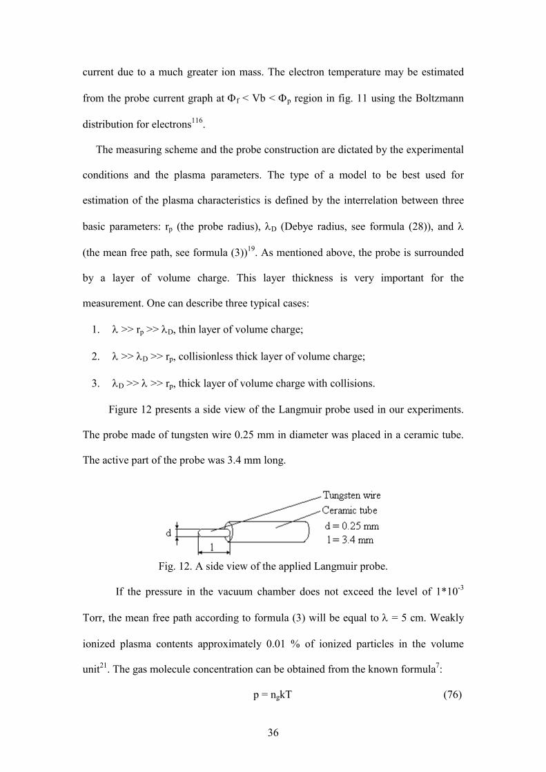
Figure 12 presents a side view of the Langmuir probe used in our experiments.
The probe made of tungsten wire 0.25 mm in diameter was placed in a ceramic tube.
The active part of the probe was 3.4 mm long.
Fig. 12. A side view of the applied Langmuir probe.
If the pressure in the vacuum chamber does not exceed the level of 1*10-3
Torr, the mean free path according to formula (3) will be equal to λ = 5 cm. Weakly
ionized plasma contents approximately 0.01 % of ionized particles in the volume
unit21. The gas molecule concentration can be obtained from the known formula7:
p = ngkT (76)
37
Here p is the pressure in the vacuum chamber, ng molecule concentration, and T
the gas temperature. Therefore, the electron concentration in the argon atmosphere
with the pressure of 1*10-3 Torr, is approximately 3.56*109 cm-3. If we assume that
the electron temperature of the weakly ionized plasma is ~ 1 - 10 eV4, 115 (see page
13), the Debye radius will be equal to approximately λD = 0.125 0.395 mm (from
formula (28)). Comparison of the parameters rp, λD, and λ shows that they satisfy the
second case: λ >> λD >> rp: collisionless thick layer of the volume charge. In this case
we can estimate the electron temperature in the plasma from the experimental I-V
characteristics of the Langmuir probe, using the known formula19:
In such a way, the electron temperature is equal to the slope angle of the Langmuir
probe characteristic in the semi-logarithmic scale. This ideal characteristic ignores
the perturbation processes such as bombardment of the probe by high-energy
electrons, emission of secondary electrons from the probe, and etching away of the
probe.
The collisionless condition allows us to use the Bohm approximation45 to
estimate the ion concentration in the plasma:
where jis is the probe current saturation density and vB is the Bohm velocity.
(77) dV
JlndkeT
-1
B
ee
=
(78) mkT
envenji
eiBiis =≈

38
2.4.4 Practical Langmuir probe measurement.
Figure 13 presents the electrical schematic diagram of Langmuir probe measurement.
The measuring probe was placed in the plasma and supplied by the bias voltage
ranging from 40 V up to + 40 V through the resistor R = 5.7 Ω.
Fig. 13. Principal electrical scheme of the Langmuir probe measurement.
Measurements were taken in various points of the plasma at different pressures in the
vacuum chamber. The distance a between the Langmuir probe and the plasma axis
(see figure 14) was also varied in the experimental trials.
Fig. 14. Dimensions of the setup interior arrangement (mm)
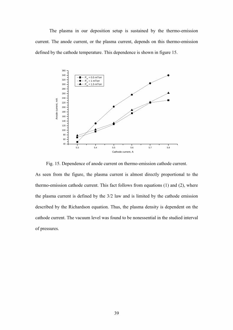
39
The plasma in our deposition setup is sustained by the thermo-emission
current. The anode current, or the plasma current, depends on this thermo-emission
defined by the cathode temperature. This dependence is shown in figure 15.
Fig. 15. Dependence of anode current on thermo-emission cathode current.
As seen from the figure, the plasma current is almost directly proportional to the
thermo-emission cathode current. This fact follows from equations (1) and (2), where
the plasma current is defined by the 3/2 law and is limited by the cathode emission
described by the Richardson equation. Thus, the plasma density is dependent on the
cathode current. The vacuum level was found to be nonessential in the studied interval
of pressures.
5.3 5.4 5.5 5.6 5.7 5.8
40
60
80
100
120
140
160
180
200
220
240
260
280
300
320
340
360
PAr = 0.5 mTorr PAr = 1 mTorr PAr = 1.5 mTorr
Anod
e cu
rrent
, mA
Cathode current, A
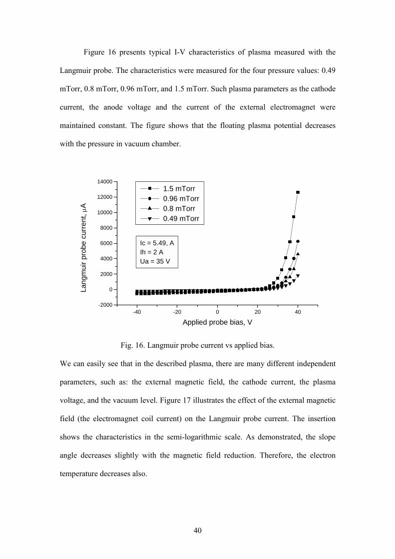
40
Figure 16 presents typical I-V characteristics of plasma measured with the
Langmuir probe. The characteristics were measured for the four pressure values: 0.49
mTorr, 0.8 mTorr, 0.96 mTorr, and 1.5 mTorr. Such plasma parameters as the cathode
current, the anode voltage and the current of the external electromagnet were
maintained constant. The figure shows that the floating plasma potential decreases
with the pressure in vacuum chamber.
Fig. 16. Langmuir probe current vs applied bias.
We can easily see that in the described plasma, there are many different independent
parameters, such as: the external magnetic field, the cathode current, the plasma
voltage, and the vacuum level. Figure 17 illustrates the effect of the external magnetic
field (the electromagnet coil current) on the Langmuir probe current. The insertion
shows the characteristics in the semi-logarithmic scale. As demonstrated, the slope
angle decreases slightly with the magnetic field reduction. Therefore, the electron
temperature decreases also.
-40 -20 0 20 40-2000
0
2000
4000
6000
8000
10000
12000
14000
Ic = 5.49, AIh = 2 AUa = 35 V
1.5 mTorr 0.96 mTorr 0.8 mTorr 0.49 mTorr
Lang
mui
r pro
be c
urre
nt, µ
A
Applied probe bias, V
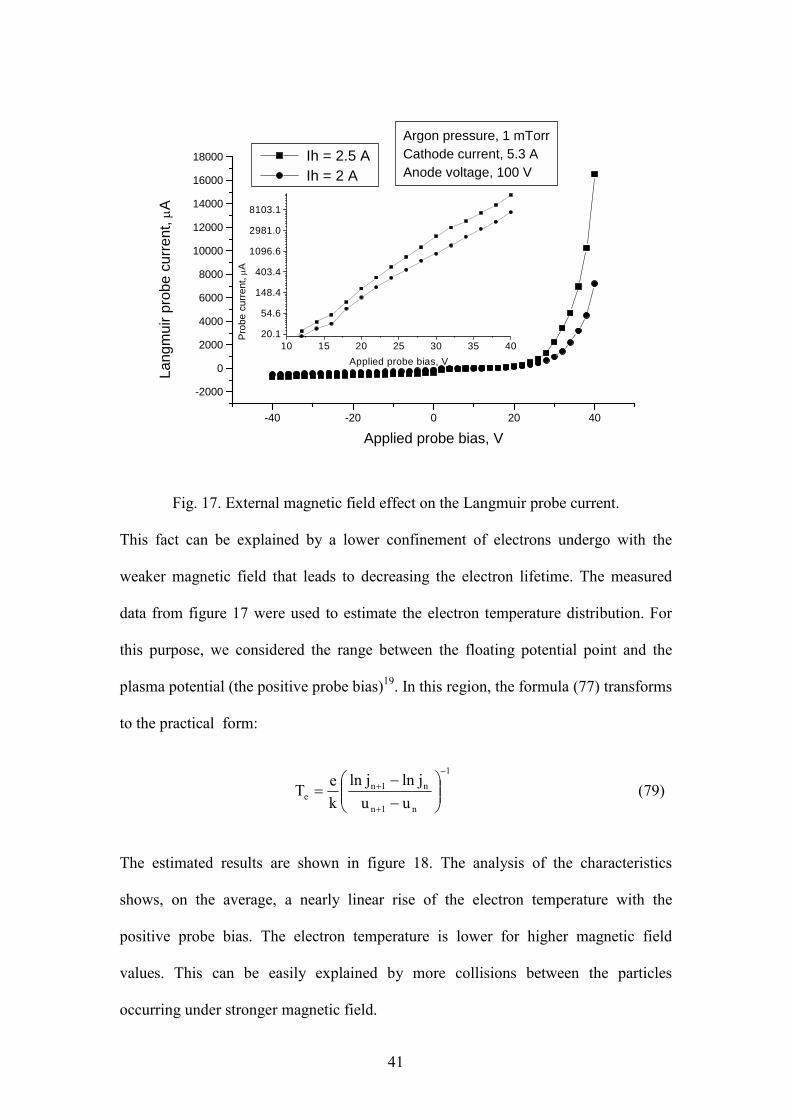
41
-40 -20 0 20 40
-2000
0
2000
4000
6000
8000
10000
12000
14000
16000
18000
Argon pressure, 1 mTorrCathode current, 5.3 AAnode voltage, 100 V
Ih = 2.5 A Ih = 2 A
Lang
mui
r pro
be c
urre
nt, µ
A
Applied probe bias, V
Fig. 17. External magnetic field effect on the Langmuir probe current.
This fact can be explained by a lower confinement of electrons undergo with the
weaker magnetic field that leads to decreasing the electron lifetime. The measured
data from figure 17 were used to estimate the electron temperature distribution. For
this purpose, we considered the range between the floating potential point and the
plasma potential (the positive probe bias)19. In this region, the formula (77) transforms
to the practical form:
The estimated results are shown in figure 18. The analysis of the characteristics
shows, on the average, a nearly linear rise of the electron temperature with the
positive probe bias. The electron temperature is lower for higher magnetic field
values. This can be easily explained by more collisions between the particles
occurring under stronger magnetic field.
(79) uu
jlnjlnkeT
1
n1n
n1ne
−
+
+
−−
=
10 15 20 25 30 35 4020.1
54.6
148.4
403.4
1096.6
2981.0
8103.1
Prob
e cu
rrent
, µA
Applied probe bias, V
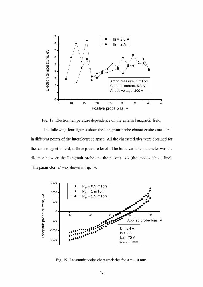
42
Fig. 18. Electron temperature dependence on the external magnetic field.
The following four figures show the Langmuir probe characteristics measured
in different points of the interelectrode space. All the characteristics were obtained for
the same magnetic field, at three pressure levels. The basic variable parameter was the
distance between the Langmuir probe and the plasma axis (the anode-cathode line).
This parameter a was shown in fig. 14.
-40 -20 0 20 40
-1500
-1000
-500
0
500
1000
1500
Ic = 5.4 AIh = 2 AUa = 70 Va = - 10 mm
PAr = 0.5 mTorr PAr = 1 mTorr PAr = 1.5 mTorr
Lang
mui
r pro
be c
urre
nt, µ
A
Applied probe bias, V
Fig. 19. Langmuir probe characteristics for a = -10 mm.
5 10 15 20 25 30 35 40 450
1
2
3
4
5
6
7
8
9
Argon pressure, 1 mTorrCathode current, 5.3 AAnode voltage, 100 V
Ih = 2.5 A Ih = 2 A
Elec
tron
tem
pera
ture
, eV
Positive probe bias, V
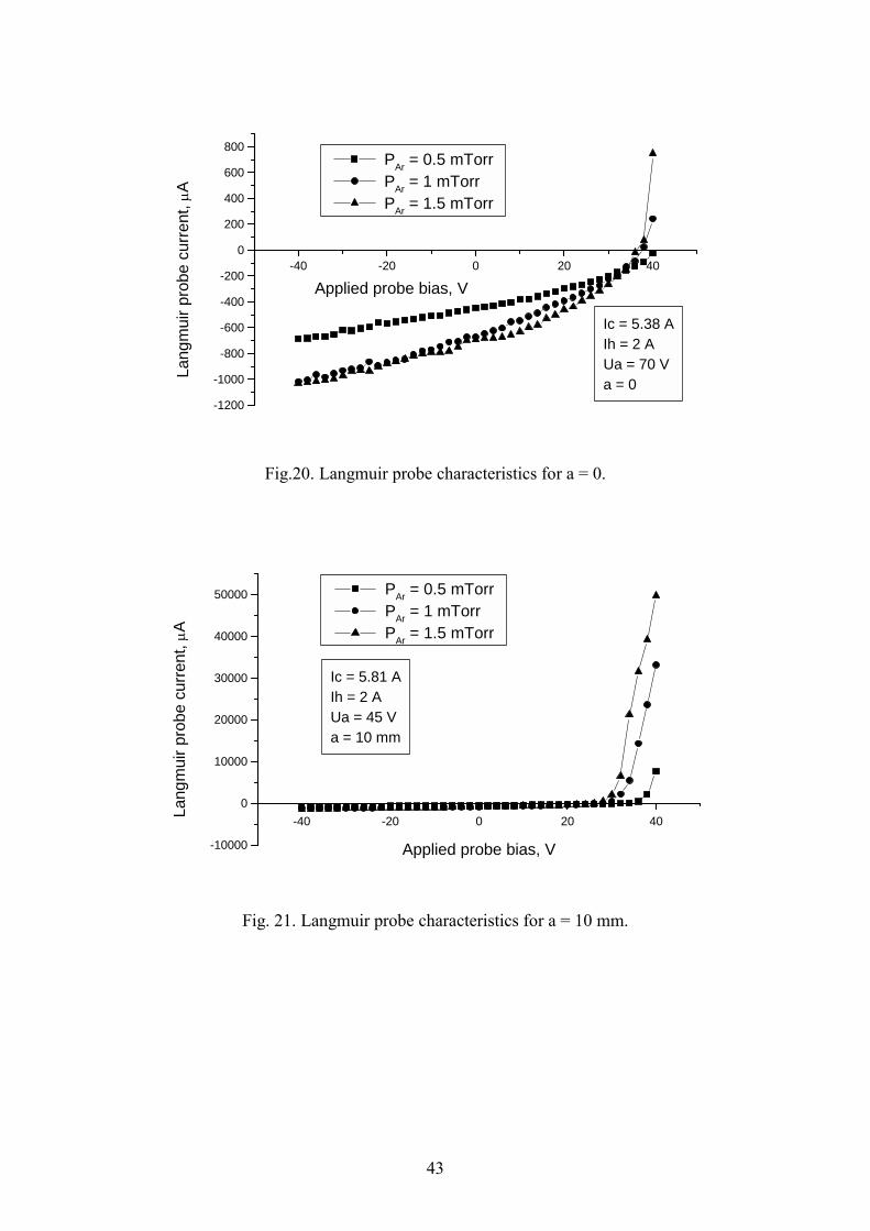
43
-40 -20 0 20 40
-1200
-1000
-800
-600
-400
-200
0
200
400
600
800
Ic = 5.38 AIh = 2 AUa = 70 Va = 0
PAr = 0.5 mTorr PAr = 1 mTorr PAr = 1.5 mTorr
Lang
mui
r pro
be c
urre
nt, µ
A
Applied probe bias, V
Fig.20. Langmuir probe characteristics for a = 0.
-40 -20 0 20 40
-10000
0
10000
20000
30000
40000
50000
Ic = 5.81 AIh = 2 AUa = 45 Va = 10 mm
PAr = 0.5 mTorr PAr = 1 mTorr PAr = 1.5 mTorr
Lang
mui
r pro
be c
urre
nt, µ
A
Applied probe bias, V
Fig. 21. Langmuir probe characteristics for a = 10 mm.
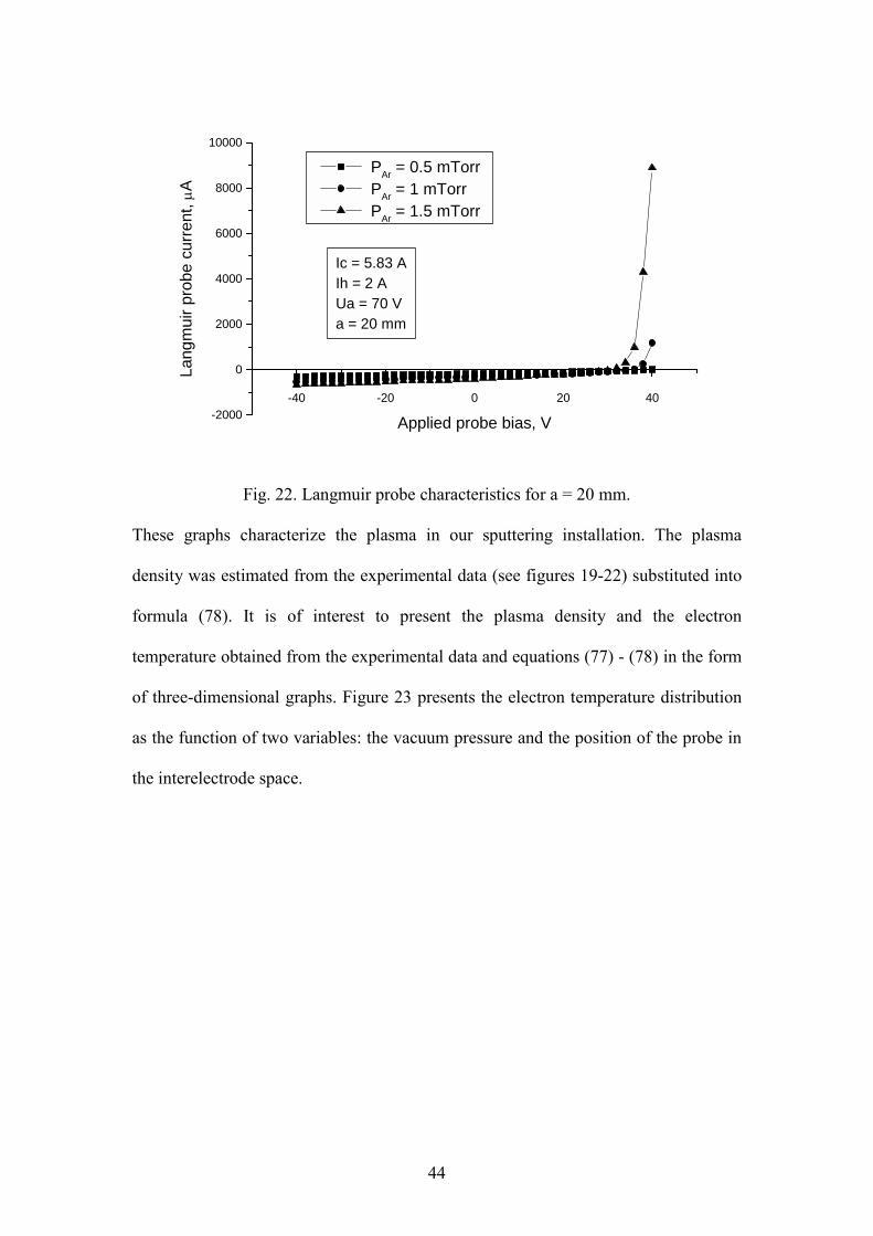
44
-40 -20 0 20 40-2000
0
2000
4000
6000
8000
10000
Ic = 5.83 AIh = 2 AUa = 70 Va = 20 mm
PAr = 0.5 mTorr PAr = 1 mTorr PAr = 1.5 mTorr
Lang
mui
r pro
be c
urre
nt, µ
A
Applied probe bias, V
Fig. 22. Langmuir probe characteristics for a = 20 mm.
These graphs characterize the plasma in our sputtering installation. The plasma
density was estimated from the experimental data (see figures 19-22) substituted into
formula (78). It is of interest to present the plasma density and the electron
temperature obtained from the experimental data and equations (77) - (78) in the form
of three-dimensional graphs. Figure 23 presents the electron temperature distribution
as the function of two variables: the vacuum pressure and the position of the probe in
the interelectrode space.

45
Fig. 23. Electron temperature of plasma in the interelectrode space.
0.500.75
1.001.25
1.50 -10
0
10
3.5
4.0
4.5
5.0
5.5
6.0
6.5
7.0
7.5
8.0
8.5
9.0
Plas
ma
dens
ity, *
1011
cm
-3
Distan
ce fr
om th
e
plasm
a axis
(a),
mm
Argon pressure, mTorr
Fig. 24. Effect of argon pressure on plasma density.
0.500.75
1.001.25
1.50 -10
0
10
2.02.53.03.54.04.5
5.0
5.5
6.0
6.5
7.0
7.5
8.0El
ectro
n te
mpe
ratu
re, e
V
Distan
ce fr
om th
e
plasm
a axis
(a),
mm
Argon pressure, mTorr
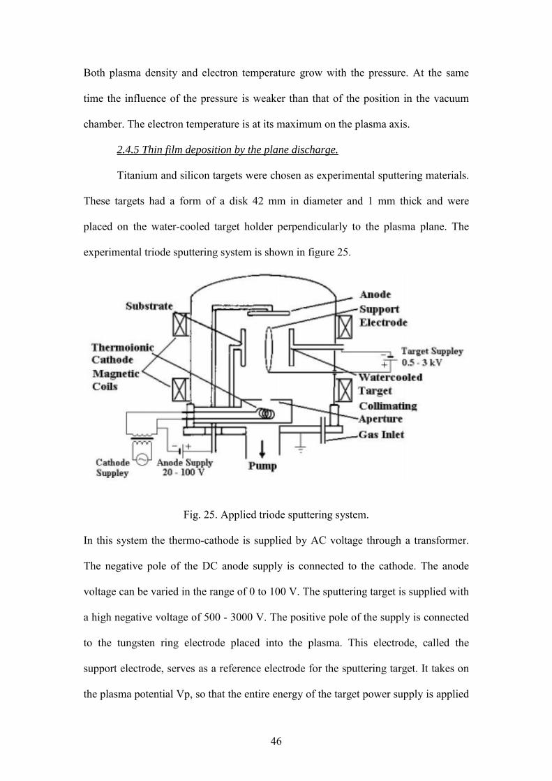
46
Both plasma density and electron temperature grow with the pressure. At the same
time the influence of the pressure is weaker than that of the position in the vacuum
chamber. The electron temperature is at its maximum on the plasma axis.
2.4.5 Thin film deposition by the plane discharge.
Titanium and silicon targets were chosen as experimental sputtering materials.
These targets had a form of a disk 42 mm in diameter and 1 mm thick and were
placed on the water-cooled target holder perpendicularly to the plasma plane. The
experimental triode sputtering system is shown in figure 25.
Fig. 25. Applied triode sputtering system.
In this system the thermo-cathode is supplied by AC voltage through a transformer.
The negative pole of the DC anode supply is connected to the cathode. The anode
voltage can be varied in the range of 0 to 100 V. The sputtering target is supplied with
a high negative voltage of 500 - 3000 V. The positive pole of the supply is connected
to the tungsten ring electrode placed into the plasma. This electrode, called the
support electrode, serves as a reference electrode for the sputtering target. It takes on
the plasma potential Vp, so that the entire energy of the target power supply is applied
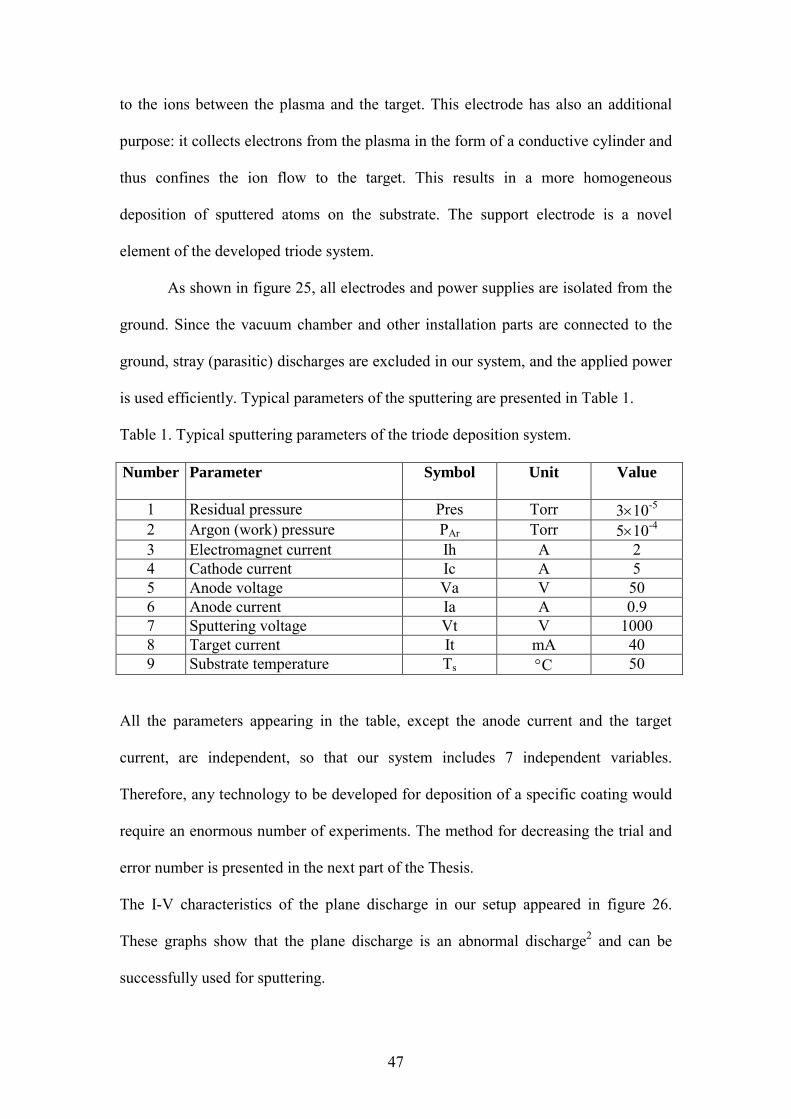
47
to the ions between the plasma and the target. This electrode has also an additional
purpose: it collects electrons from the plasma in the form of a conductive cylinder and
thus confines the ion flow to the target. This results in a more homogeneous
deposition of sputtered atoms on the substrate. The support electrode is a novel
element of the developed triode system.
As shown in figure 25, all electrodes and power supplies are isolated from the
ground. Since the vacuum chamber and other installation parts are connected to the
ground, stray (parasitic) discharges are excluded in our system, and the applied power
is used efficiently. Typical parameters of the sputtering are presented in Table 1.
Table 1. Typical sputtering parameters of the triode deposition system.
Number Parameter Symbol Unit Value
1 Residual pressure Pres Torr 3×10⁻⁵ 2 Argon (work) pressure PAr Torr 5×10⁻⁴ 3 Electromagnet current Ih A 2 4 Cathode current Ic A 5 5 Anode voltage Va V 50 6 Anode current Ia A 0.9 7 Sputtering voltage Vt V 1000 8 Target current It mA 40 9 Substrate temperature Ts °C 50
All the parameters appearing in the table, except the anode current and the target
current, are independent, so that our system includes 7 independent variables.
Therefore, any technology to be developed for deposition of a specific coating would
require an enormous number of experiments. The method for decreasing the trial and
error number is presented in the next part of the Thesis.
The I-V characteristics of the plane discharge in our setup appeared in figure 26.
These graphs show that the plane discharge is an abnormal discharge2 and can be
successfully used for sputtering.

48
Fig. 26. Discharge current as a function of the applied voltage.
The discharge current is influenced by the argon pressure and the cathode current.
Fig. 27 shows the effect of the argon pressure on the discharge current for two
different values of the cathode current.
Fig. 27. Discharge current as a function of argon pressure.
The plasma (discharge) current is defined by the electron emission from the cathode
and the concentration of argon atoms in the vacuum chamber.
10 20 30 40 50 600
200
400
600
800
1000
PAr = 1.1 mTorr
Ic = 3.22 A Ic = 3.50 A Ic = 3.49 A
Dis
char
ge c
urre
nt, m
A
Applied discharge voltage, V
0.6 0.7 0.8 0.9 1.0 1.1 1.2500
600
700
800
900
1000
Ic = 3.50 A Ic = 3.49 A
Dis
char
ge c
urre
nt, m
A
Argon pressure, mTorr
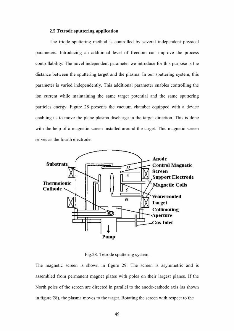
49
2.5 Tetrode sputtering application
The triode sputtering method is controlled by several independent physical
parameters. Introducing an additional level of freedom can improve the process
controllability. The novel independent parameter we introduce for this purpose is the
distance between the sputtering target and the plasma. In our sputtering system, this
parameter is varied independently. This additional parameter enables controlling the
ion current while maintaining the same target potential and the same sputtering
particles energy. Figure 28 presents the vacuum chamber equipped with a device
enabling us to move the plane plasma discharge in the target direction. This is done
with the help of a magnetic screen installed around the target. This magnetic screen
serves as the fourth electrode.
Fig.28. Tetrode sputtering system.
The magnetic screen is shown in figure 29. The screen is asymmetric and is
assembled from permanent magnet plates with poles on their largest planes. If the
North poles of the screen are directed in parallel to the anode-cathode axis (as shown
in figure 28), the plasma moves to the target. Rotating the screen with respect to the

50
target axis around the target holder varies the distance between the plasma and the
target.
Fig. 29. External view of the magnetic screen.
The dependence of the target current on the magnetic screen direction is shown in
figure 30.
1 2 330
32
34
36
38
40
42
44
46
48
1 - without magnetic screen2 - S-S position of the magnet3 - N-N position of the magnet
Targ
et c
urre
nt, m
A
Magnetic screen position
Fig. 30. Target current versus magnetic screen position.
This influence can be explained by interaction of two magnetic fields: the external
homogeneous magnetic field and the asymmetrical magnetic field of the control
screen. Plasma as a conductive substance is affected by magnetic fields. The

51
intersection of the magnetic fields serves as a trap for the plasma body and moves it in
the corresponding direction.
We have evaluated the mechanical and electrical properties of the Si and Ti
thin films deposited by the described sputtering method. The sheet resistance was
measured with a standard four-point probe method, and the film thickness was found
by a Tencor Instruments profilometer. The film surface structure was studied on a
Leica Stereoscan 430 Scanning Electron Microscope (SEM) operating in 20 KeV. The
composition of the deposited films was evaluated by the Energy Dispersive
Spectrometry (EDS) method, with the help of the add-on EDS device mounted on the
STEREOSCAN-430. The microhardness of deposited films was measured using a
standard tester PMT-3 manufactured in Russia65, 66. The indentation period was 15
seconds; 5-10 indentations were taken for each specimen. The glass substrates were
cleaned with isoprophanol.
All the films were semi-transparent (they were thin), since the sputtering
duration did not exceed 15 min in all the trials. The method has revealed high
deposition rates. Table 2 presents the deposition rates compared to the data obtained
by ion beam sputtering method and reported by J.P. Greene43.
Table 2. Sputtering deposition rates with Argon, Å/min (Vt = 1000 V).
Element Ref [43] Ref [44] Our results Titanium 50 21 60 Silicon - 35 100
The deposition of Ti films was carried out with the sputtering voltage of 1000 V and
the Argon pressure of 1×10⁻³ Torr. The target current was 46 mA, and the control
magnetic screen was placed in the N-N position (see fig. 30). The obtained Ti film
was 600 Å thick and its microhardness was ~ 315 kG/mm2.
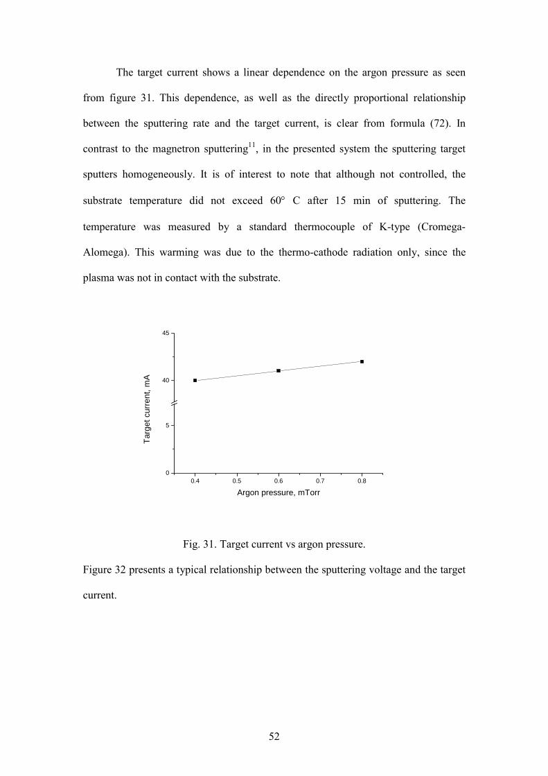
52
The target current shows a linear dependence on the argon pressure as seen
from figure 31. This dependence, as well as the directly proportional relationship
between the sputtering rate and the target current, is clear from formula (72). In
contrast to the magnetron sputtering11, in the presented system the sputtering target
sputters homogeneously. It is of interest to note that although not controlled, the
substrate temperature did not exceed 60° C after 15 min of sputtering. The
temperature was measured by a standard thermocouple of K-type (Cromega-
Alomega). This warming was due to the thermo-cathode radiation only, since the
plasma was not in contact with the substrate.
Fig. 31. Target current vs argon pressure.
Figure 32 presents a typical relationship between the sputtering voltage and the target
current.
0.4 0.5 0.6 0.7 0.80
5
40
45
Targ
et c
urre
nt, m
A
Argon pressure, mTorr

53
Fig. 32. Target current vs sputtering voltage.
Figure 33 presents the sheet resistance measured for the Ti films deposited
under different deposition conditions. Obviously, the deposition rate affects the film
thickness, and the sheet resistance is defined by the film thickness and density.
Fig. 33. Sheet resistance of Ti films measured by four-point probe method.
200 400 600 800 1000 1200 1400 1600
20
25
30
35
40
45
Targ
et c
urre
nt, m
A
Sputtering voltage, V
0.0 0.2 0.4 0.6 0.8 1.0 1.2 1.4 1.60
5
10
15
20
25
Ti film, S-S position Ti film, N-N positionM
easu
red
volta
ge, m
V
Applied current, mA

54
The sheet resistance was measured for Si films as well. These data appearing in figure
34 also show a directly proportional I-V dependence.
Fig. 34. Sheet resistance of Si films measured by four-point probe method.
These films were deposited with two different sets of deposition parameters, as shown
in table 3.
Table 3. Sputtering deposition parameters used for the Si films deposition.
Pres PAr Ic Ih Va Ia Ut It t El/m R# Units Torr mTorr A A V mA V mA min Ω/sq.N1 4×10⁻⁵ 0.7 3.5 2 55 930 1000 36 10 - 23.96N2 4×10⁻⁵ 0.5 3.1 2 55 740 1500 32 15 N-N 41.16
The data appearing in Table 3 shows a good possibility for fine control of the
deposited film properties. The microhardness of the silicon semi-transparent film was
found to be 465 kG/mm2. This value is sufficiently high for thin Si films, as compared
to the bulk crystalline silicon, which has the microhardness of ~1000 kG/mm2.
0.4 0.6 0.8 1.0 1.2 1.4 1.6 1.8 2.0 2.2
3456789
10111213141516171819
Si film, N1 Si film, N2
Mea
sure
d vo
ltage
, mV
Applied current, mA
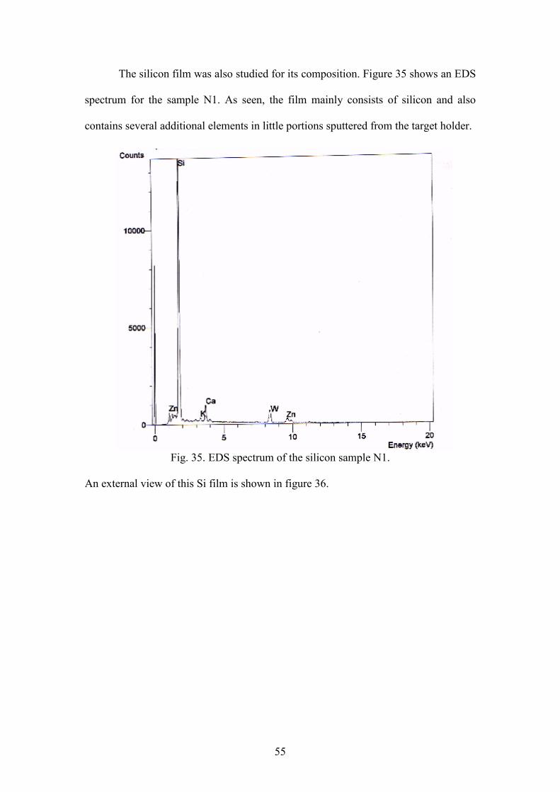
55
The silicon film was also studied for its composition. Figure 35 shows an EDS
spectrum for the sample N1. As seen, the film mainly consists of silicon and also
contains several additional elements in little portions sputtered from the target holder.
Fig. 35. EDS spectrum of the silicon sample N1.
An external view of this Si film is shown in figure 36.
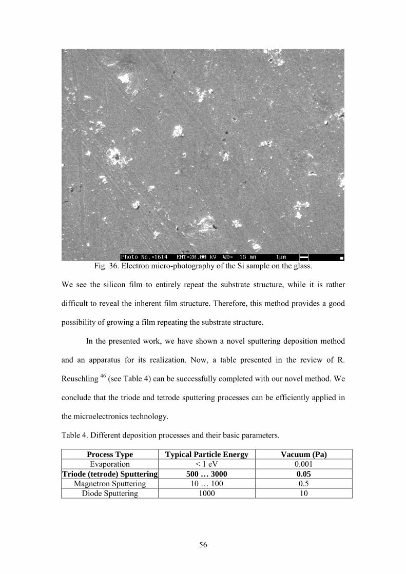
56
Fig. 36. Electron micro-photography of the Si sample on the glass.
We see the silicon film to entirely repeat the substrate structure, while it is rather
difficult to reveal the inherent film structure. Therefore, this method provides a good
possibility of growing a film repeating the substrate structure.
In the presented work, we have shown a novel sputtering deposition method
and an apparatus for its realization. Now, a table presented in the review of R.
Reuschling 46 (see Table 4) can be successfully completed with our novel method. We
conclude that the triode and tetrode sputtering processes can be efficiently applied in
the microelectronics technology.
Table 4. Different deposition processes and their basic parameters.
Process Type Typical Particle Energy Vacuum (Pa) Evaporation < 1 eV 0.001
Triode (tetrode) Sputtering 500 … 3000 0.05 Magnetron Sputtering 10 100 0.5
Diode Sputtering 1000 10
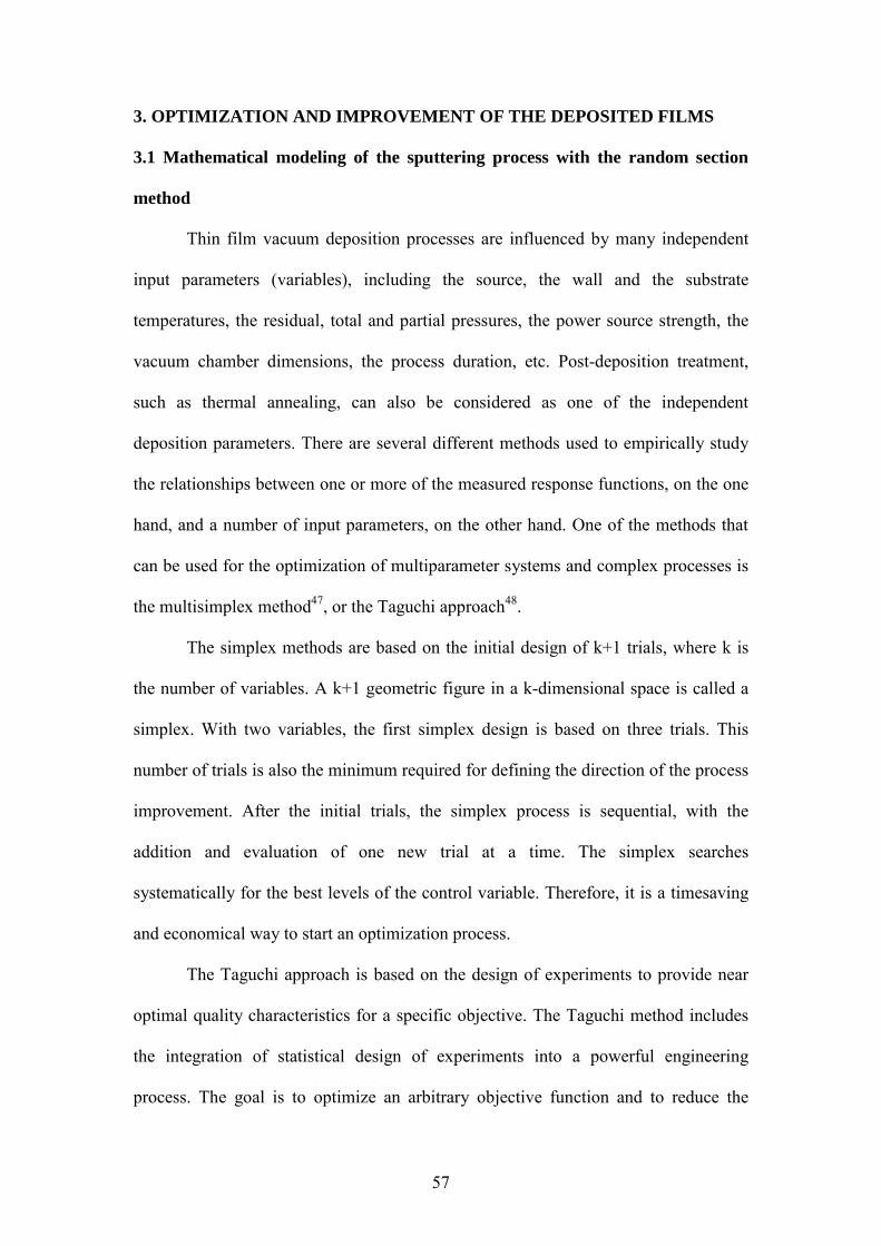
57
3. OPTIMIZATION AND IMPROVEMENT OF THE DEPOSITED FILMS
3.1 Mathematical modeling of the sputtering process with the random section
method
Thin film vacuum deposition processes are influenced by many independent
input parameters (variables), including the source, the wall and the substrate
temperatures, the residual, total and partial pressures, the power source strength, the
vacuum chamber dimensions, the process duration, etc. Post-deposition treatment,
such as thermal annealing, can also be considered as one of the independent
deposition parameters. There are several different methods used to empirically study
the relationships between one or more of the measured response functions, on the one
hand, and a number of input parameters, on the other hand. One of the methods that
can be used for the optimization of multiparameter systems and complex processes is
the multisimplex method47, or the Taguchi approach48.
The simplex methods are based on the initial design of k+1 trials, where k is
the number of variables. A k+1 geometric figure in a k-dimensional space is called a
simplex. With two variables, the first simplex design is based on three trials. This
number of trials is also the minimum required for defining the direction of the process
improvement. After the initial trials, the simplex process is sequential, with the
addition and evaluation of one new trial at a time. The simplex searches
systematically for the best levels of the control variable. Therefore, it is a timesaving
and economical way to start an optimization process.
The Taguchi approach is based on the design of experiments to provide near
optimal quality characteristics for a specific objective. The Taguchi method includes
the integration of statistical design of experiments into a powerful engineering
process. The goal is to optimize an arbitrary objective function and to reduce the

58
sensitivity of engineering designs to uncontrollable parameters or noise. The objective
function used and maximized in the present case is the signal-to-noise ratio. This
method involves three steps of the optimization process:
1. System design (development of a system designed to function under nominal
conditions, with a given initial set of input parameters);
2. Parameter design (selection of optimal levels for the controllable system
parameters);
3. Tolerance design (a narrower tolerance range must be specified for those design
factors whose variation imparts a large negative influence on the output
function).
The Taguchi method can significantly reduce the number of experiments needed to
find the response function, by improving the efficiency of generating information
needed for the system design.
The response surface methodology (RSM) is an optimization approach, which
uses mathematical and statistical techniques to search for the best combination of the
process variables. The response surface represents the domain of all feasible solutions
for the process model49. The response surface approach is the best method for an
empirical study of the relationships between one or more of the measured response
functions such as resistivity, transparency, density, on the one hand, and various input
parameters, on the other hand50. After such a study, the RSM method enables the
process optimization with a minimum of trial and errors. If the process model is
presented as mathematical function, one can say that the response surface is a trace of
the response function (the main parameter) in the multi-parameter space. Then it can
be written in the form of F = f(X1,X2,..Xm), where X1, X2, and Xm are the
independently controlled measured input variables of the sputtering process.

59
In the narrow interval of the variation of the input variables, the
response function may be considered as an analytical function. The approximation
process may begin as a polynomial model with linear independent coefficients51.
Therefore, it may be expanded in a Taylor series over the chosen area in the form:
(80) )xx(!n
)x(f)x(f n0
0n
0)n(
−= ∑∞
=
By choosing the first three terms of the above expansion, a second order
approximation is obtained:
(81) )xx(dx
)x(fd21)xx(
dx)x(df)x(f)x(f 2
020
2
00
0 −+−+=
This expression has the form of a parabolic function with linear coefficients:
f(x) = a + bx + cx2 (82)
For a multi-parameter process of m levels, i.e. with m independently controlled
measured input variables, the expression is transformed to a model of the following
type, without the high order (in our case, third order) interaction effects:
F = c0 + c1X1 + c2X2 + c3X3 + + cmX1m + cm+1X1X2 + cm+2X1X3 +
+ + ckXm-1Xm + ck+1X12 + ck+2X2
2 + + ck+mXm2 (83)
where F is the response function, ci are the model coefficients, and Xi are the
processing parameters.
A standard form for a planned series of experiments for evaluating the normalized
process parameters is shown in table 5 52. The parameters are normalized using the
following equation:
Xi* = 2(Xi X0)/∆X (84)
where X0 is the midpoint of the variable range, and ∆X is the variation range.
Table 5. Standard form for model coefficient estimation: F is the response function
and Xi* are the normalized process parameters.
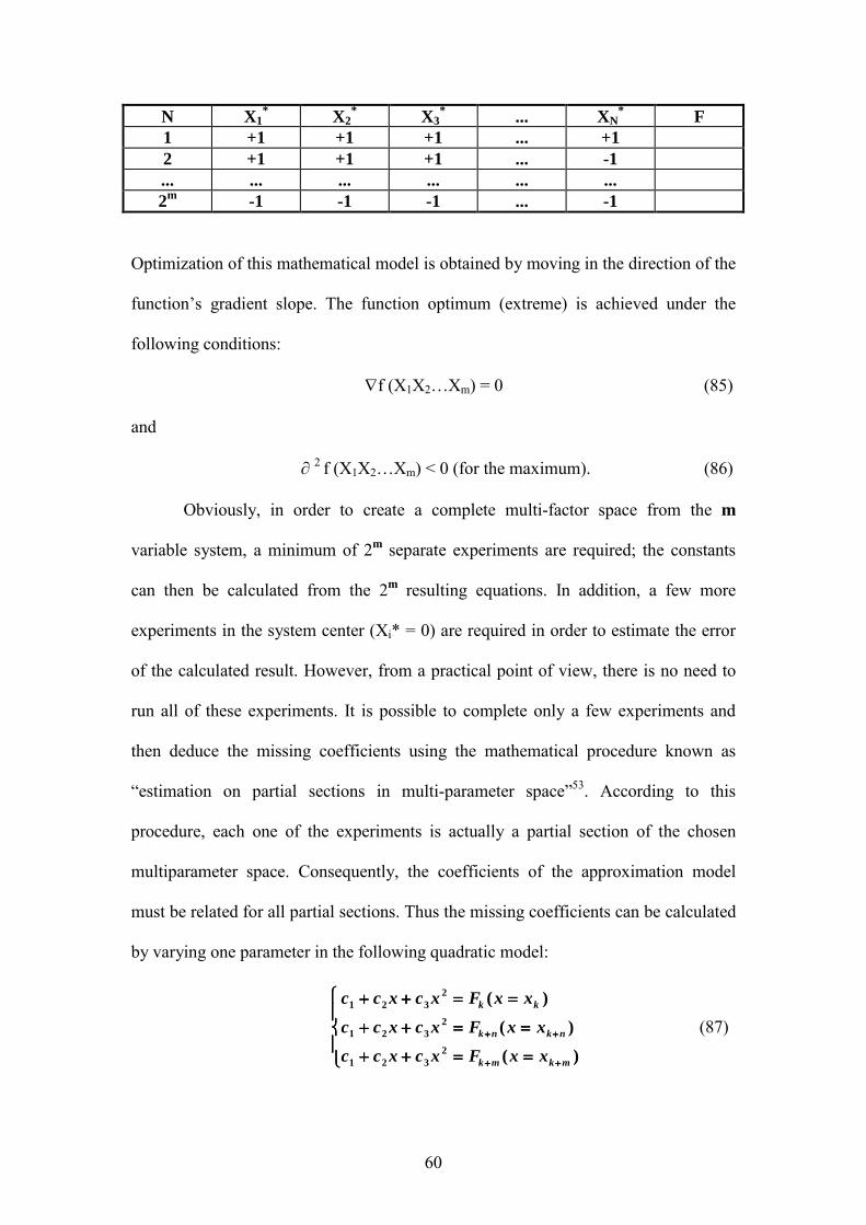
60
N X1* X2
* X3* ... XN
* F 1 +1 +1 +1 ... +1 2 +1 +1 +1 ... -1 ... ... ... ... ... ... 2m -1 -1 -1 ... -1
Optimization of this mathematical model is obtained by moving in the direction of the
functions gradient slope. The function optimum (extreme) is achieved under the
following conditions:
∇f (X1X2Xm) = 0 (85)
and
∂ 2 f (X1X2Xm) < 0 (for the maximum). (86)
Obviously, in order to create a complete multi-factor space from the m
variable system, a minimum of 2m separate experiments are required; the constants
can then be calculated from the 2m resulting equations. In addition, a few more
experiments in the system center (Xi* = 0) are required in order to estimate the error
of the calculated result. However, from a practical point of view, there is no need to
run all of these experiments. It is possible to complete only a few experiments and
then deduce the missing coefficients using the mathematical procedure known as
estimation on partial sections in multi-parameter space53. According to this
procedure, each one of the experiments is actually a partial section of the chosen
multiparameter space. Consequently, the coefficients of the approximation model
must be related for all partial sections. Thus the missing coefficients can be calculated
by varying one parameter in the following quadratic model:
c c x c x F x xc c x c x F x xc c x c x F x x
k k
k n k n
k m k m
1 2 32
1 2 32
1 2 32
++++ ++++ ==== ====
++++ ++++ ==== ====
++++ ++++ ==== ====
++++ ++++
++++ ++++
( )( )( )
(87)

61
where ci is the missing coefficient, x the process parameter (X1,X2,..XN), F the
response function, and m, n are indices. The rest of the missing coefficients describing
the required model are then obtained by solving the coefficient matrix with the
Kramer method.
In the case of a large deviation between the measured data and the model, the
approximation order, i.e. the order of approximation equation, should be increased.
3.1.1 Deposition of In2O3 conductive transparent coatings by DC sputtering
3.1.1.1 Introduction.
Transparent conductive coatings with high electrical conductivity and the
maximum optical transparency attracted much attention in recent years. These
coatings have many practical applications, such as, for instance, transparent electrodes
in microelectronics, optoelectronic devices and photovoltaic systems.
Indium oxide thin films possess the electronic properties of n-type
semiconductors with a band gap in the range of 3.5 to 4 eV. Oxygen vacancies in the
films provide free electrons by acting as doubly charged donors. Since the indium
oxide films generally suffer from oxygen deficiency, the electron gas in the
conduction band is degenerate54. These transparent films are often alloyed with tin
oxide (5 to 10 %); such films are known as indium tin oxide (ITO). These films have
a higher free charge concentration, which increases the electrical conductivity55, 56.
Films without the tin admixture have higher resistivity and lower transparency than
ITO57. The tin is commonly believed to provide free electrons by substituting for the
indium atoms and acting as a singly charged donor at the indium site. Other alloys of
indium oxide with elements from the IV, V or VI columns of the periodic table have
62
been reported58. An attempt to deposit by DC magnetron sputtering the insulating
indium oxide films for creating tunnel junction barrier layers has also been reported59.
Most of the unalloyed indium oxide films were prepared by different
evaporation methods. These methods had one common characteristic: injection of
oxygen in the vacuum chamber (reactive evaporation)60, 61. The influence of oxygen
on the partial pressure of the structure of the reactively deposited indium oxide films
has been described in ref. [62]. In ref. [63], the influence of the substrate temperature,
deposition rate, base and background pressures, and alloy constituents concentration
were studied. However, the films with the maximum transparency and minimum
resistivity have been prepared by sputtering 64.
Most of the literature in this field has concentrated on the physical analysis of
ITO coatings. In our work, we present a different approach to the manufacturing of
transparent conductive thin films. In addition to considering the physical properties of
the final product, we developed a mathematical model of the processing stages based
on the above mentioned response surface methodology (RSM). Using our process
model enabled us to optimize the technological parameter values more efficiently,
with a minimum number of trial runs. The modeling method was applied and tested to
the known magnetron sputtering53, 82, 117.
3.1.1.2 Experimental procedure.
The experiments were carried out on a laboratory magnetron sputtering
vacuum station (see figure 37), equipped with a diffusion pump. A principle
schematic diagram of the magnetron sputtering source is shown in figure 38. The
residual pressure prior to the deposition process was less than 4×10⁻⁵ Torr and the
sputtering was done in a pure argon atmosphere (99.996%). The substrate temperature
was varied during the deposition process and the samples underwent a post-deposition

63
heat treatment, while still in vacuum. The indium oxide films were deposited on a
borosilicate glass plate 0.13-0.17 mm thick and on an optical glass 1 mm thick. The
sputtering target was in a shape of a round disk, 50 mm in diameter and 3 mm thick,
made of pure indium oxide (99.999%). The substrate-to-target distance was taken as 5
cm.
Fig. 37. Experimental magnetron vacuum station.
We evaluated the optical and electrical properties of the resultant In2O3 films.
The optical transparency of the films and absorption for 250 < λ < 880 nm was
determined on a Uvicon 941 Plus spectrophotometer. Transparency in the IR
spectrum was measured in the range of 400 to 2500 nm. A computerized metallurgical
microscope with magnification × 80 to × 1600 was used for the microtopography
evaluation. The microhardness of the resulting films was measured using a tester
PMT-3. The indentation period was 15 seconds; 5 to 10 indentations were taken for
each specimen. The substrates were cleaned with alcohol in the ultrasound heater for
5 min.
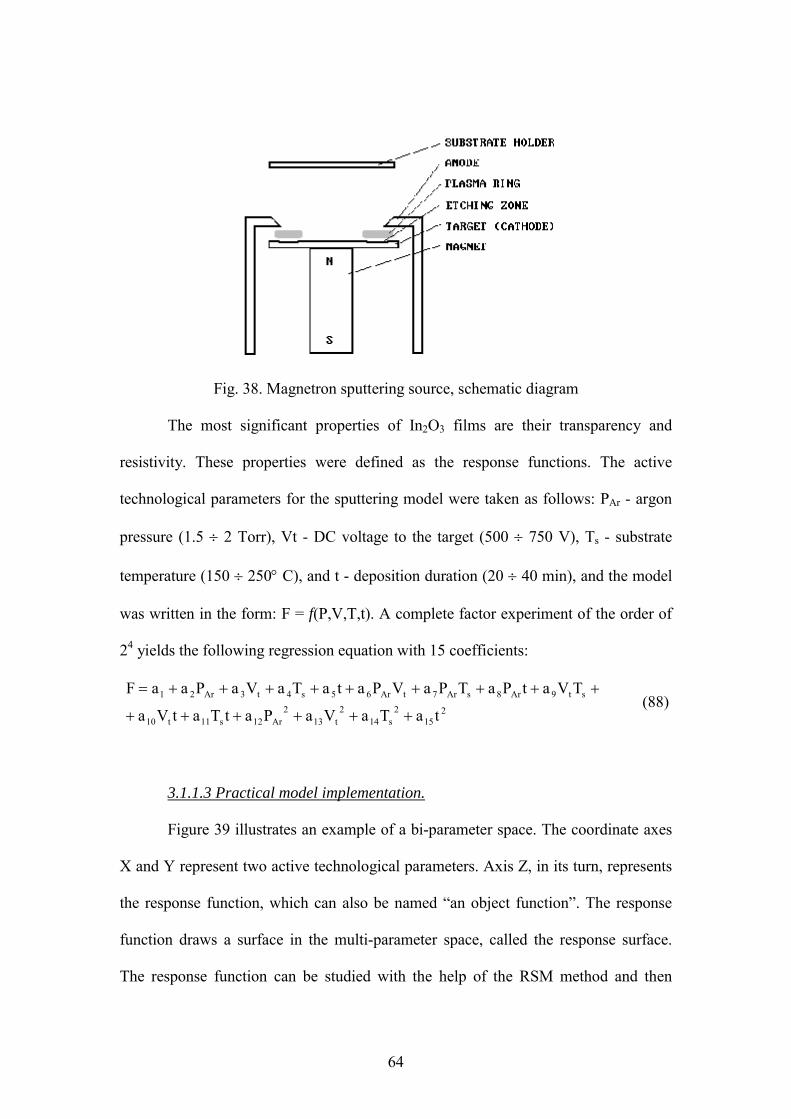
64
Fig. 38. Magnetron sputtering source, schematic diagram
The most significant properties of In2O3 films are their transparency and
resistivity. These properties were defined as the response functions. The active
technological parameters for the sputtering model were taken as follows: PAr - argon
pressure (1.5 ÷ 2 Torr), Vt - DC voltage to the target (500 ÷ 750 V), Ts - substrate
temperature (150 ÷ 250° C), and t - deposition duration (20 ÷ 40 min), and the model
was written in the form: F = f(P,V,T,t). A complete factor experiment of the order of
24 yields the following regression equation with 15 coefficients:
2
152
s142
t132
Ar12s11t10
st9Ar8sAr7tAr65s4t3Ar21
taTaVaPatTatVa
TVatPaTPaVPataTaVaPaaF
++++++
+++++++++= (88)
3.1.1.3 Practical model implementation.
Figure 39 illustrates an example of a bi-parameter space. The coordinate axes
X and Y represent two active technological parameters. Axis Z, in its turn, represents
the response function, which can also be named an object function. The response
function draws a surface in the multi-parameter space, called the response surface.
The response function can be studied with the help of the RSM method and then

65
optimized. A standard orthogonal plan for this experiment can be presented in a
tabular form (see Table 6), which is also convenient for numerical calculations50, 52.
Fig. 39. Example of bi-parameter experiment space.
This table contains the selected normalized active technological parameters: P*, V*,
T*, t* and the defined response functions. The normalization was done by formula
(84).
Table 6. Normalized active technological parameters.
N P* V* T* t* D RS 1 +1 +1 +1 +1 2 +1 +1 +1 -1
16 -1 -1 -1 -1
It is obvious that in order to create a complete 15-constant parameter space
from a 4-variables system, 15 separate experiments should be carried out. These
constants will be then calculated from the 15 obtained equations. In addition, it is
necessary to perform a few more experiments in the system center in order to obtain
an estimation of the relative experiment error. A virtual example of a multi-parameter
space experiment and a random partial section of it is shown in figure 40. Each one of
the experiments is actually a partial section of the chosen multi-parameter space.

66
Fig. 40. Illustration of random partial sections of the multi-parameter space.
These random partial sections are described by the same equations and belong to the
analytical response function. Consequently, the coefficients of the approximation
model must be equal for all partial sections. Thus the missing coefficients can be
calculated by varying one parameter using the equations (87). The rest of the missing
coefficients describing the required model are then obtained by solving the coefficient
matrix. One should always bear in mind that only the first few resultant coefficients
were experimentally obtained, while the rest of the coefficients were derived
mathematically from following matrix (i is an index):
( ) ( ) ( )ii2i
2i
2i
2iiiiiiiiiiiiiiiii Fa tT V P tT tV TV tP TP VP tT V P 1 ⋅= (89)
At this point the optimization model of equation (85) can be implemented.
Thus, the optimization problem is transformed to the following gradient relation:
0
tT V P
)t,T,V,P(F)t,T,V,P(F s
t
Ar
stAr**** =
∂∂∂∂
⋅∇=∂ , (90)
where F(P*,V*,T*,t*) is the required extreme. Analysis of this relation yields 16
possible combinations (24) between the four variables. Similarly, analysis of the
second derivative yields the type of extreme: a maximum for the transparency and a
minimum for the resistivity.
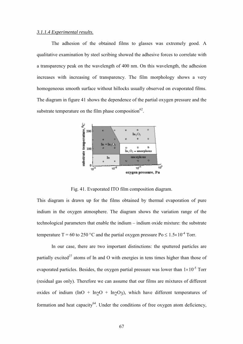
67
3.1.1.4 Experimental results.
The adhesion of the obtained films to glasses was extremely good. A
qualitative examination by steel scribing showed the adhesive forces to correlate with
a transparency peak on the wavelength of 400 nm. On this wavelength, the adhesion
increases with increasing of transparency. The film morphology shows a very
homogeneous smooth surface without hillocks usually observed on evaporated films.
The diagram in figure 41 shows the dependence of the partial oxygen pressure and the
substrate temperature on the film phase composition62.
Fig. 41. Evaporated ITO film composition diagram.
This diagram is drawn up for the films obtained by thermal evaporation of pure
indium in the oxygen atmosphere. The diagram shows the variation range of the
technological parameters that enable the indium indium oxide mixture: the substrate
temperature T = 60 to 250 °C and the partial oxygen pressure Po ≤ 1.5×10⁻⁴ Torr.
In our case, there are two important distinctions: the sputtered particles are
partially excited27 atoms of In and O with energies in tens times higher than those of
evaporated particles. Besides, the oxygen partial pressure was lower than 1×10⁻⁵ Torr
(residual gas only). Therefore we can assume that our films are mixtures of different
oxides of indium (InO + In2O + In2O3), which have different temperatures of
formation and heat capacity64. Under the conditions of free oxygen atom deficiency,
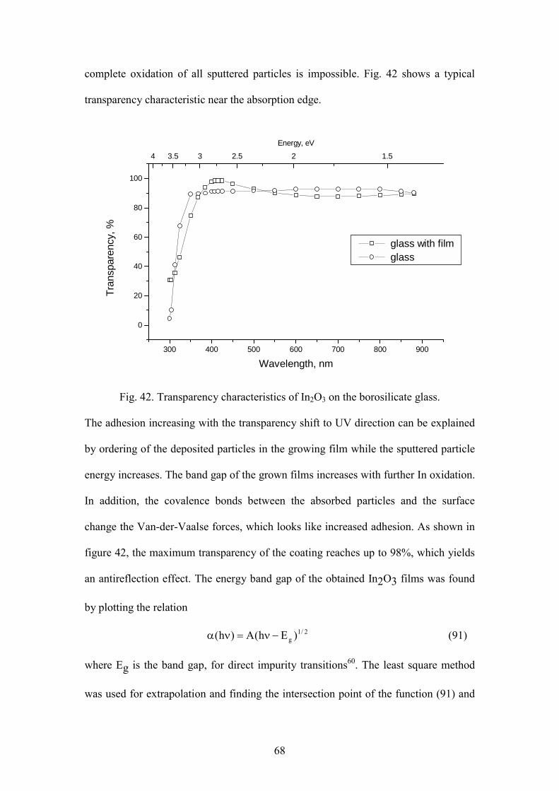
68
complete oxidation of all sputtered particles is impossible. Fig. 42 shows a typical
transparency characteristic near the absorption edge.
Fig. 42. Transparency characteristics of In2O3 on the borosilicate glass.
The adhesion increasing with the transparency shift to UV direction can be explained
by ordering of the deposited particles in the growing film while the sputtered particle
energy increases. The band gap of the grown films increases with further In oxidation.
In addition, the covalence bonds between the absorbed particles and the surface
change the Van-der-Vaalse forces, which looks like increased adhesion. As shown in
figure 42, the maximum transparency of the coating reaches up to 98%, which yields
an antireflection effect. The energy band gap of the obtained In2O3 films was found
by plotting the relation
2/1g )Eh(A)h( −ν=να (91)
where Eg is the band gap, for direct impurity transitions60. The least square method
was used for extrapolation and finding the intersection point of the function (91) and
300 400 500 600 700 800 900
0
20
40
60
80
100
glass with film glass
Tran
spar
ency
, %
Wavelength, nm
4 3.5 3 2.5 2 1.5Energy, eV
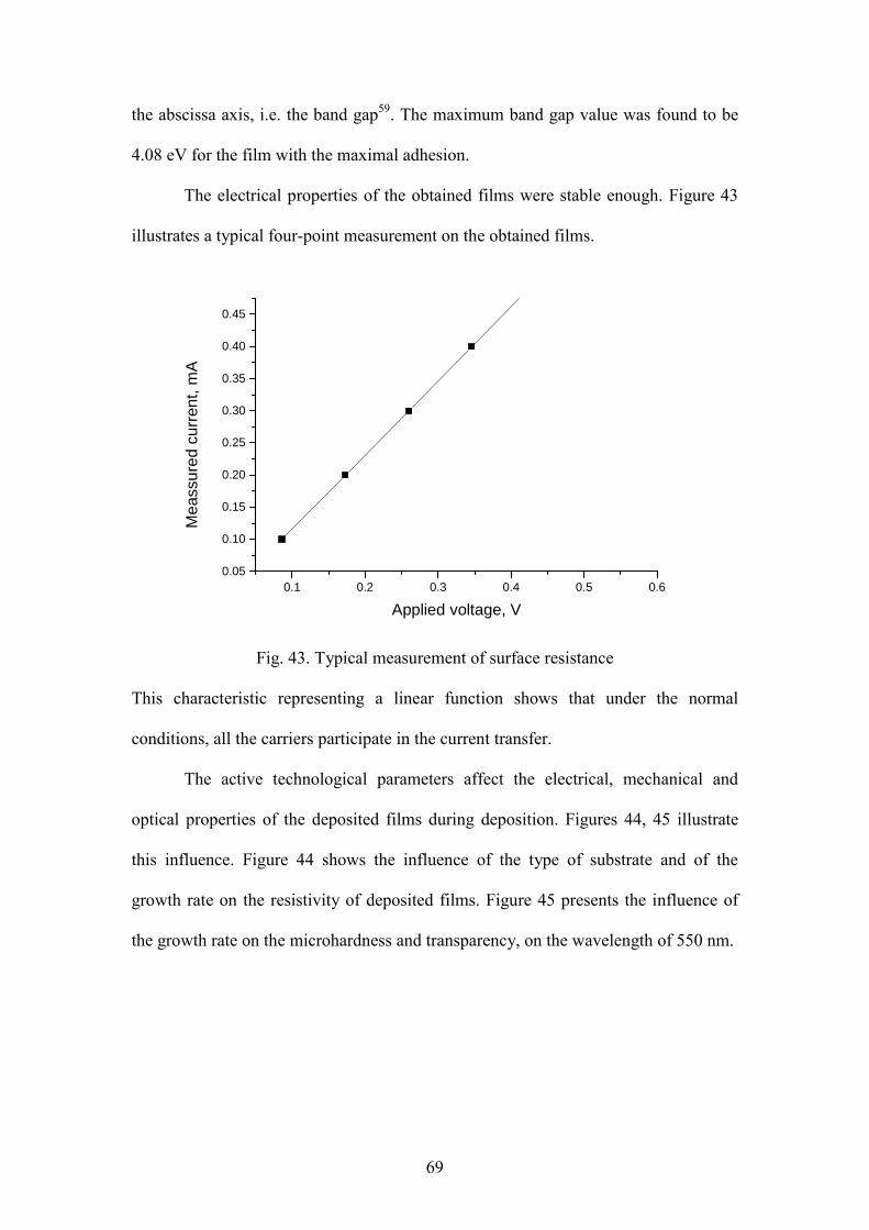
69
the abscissa axis, i.e. the band gap59. The maximum band gap value was found to be
4.08 eV for the film with the maximal adhesion.
The electrical properties of the obtained films were stable enough. Figure 43
illustrates a typical four-point measurement on the obtained films.
Fig. 43. Typical measurement of surface resistance
This characteristic representing a linear function shows that under the normal
conditions, all the carriers participate in the current transfer.
The active technological parameters affect the electrical, mechanical and
optical properties of the deposited films during deposition. Figures 44, 45 illustrate
this influence. Figure 44 shows the influence of the type of substrate and of the
growth rate on the resistivity of deposited films. Figure 45 presents the influence of
the growth rate on the microhardness and transparency, on the wavelength of 550 nm.
0.1 0.2 0.3 0.4 0.5 0.60.05
0.10
0.15
0.20
0.25
0.30
0.35
0.40
0.45
Mea
ssur
ed c
urre
nt, m
A
Applied voltage, V
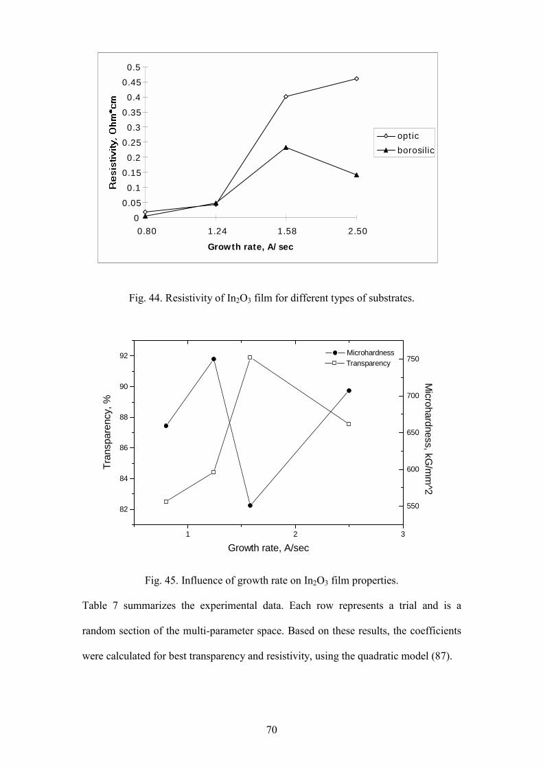
70
Fig. 44. Resistivity of In2O3 film for different types of substrates.
Fig. 45. Influence of growth rate on In2O3 film properties.
Table 7 summarizes the experimental data. Each row represents a trial and is a
random section of the multi-parameter space. Based on these results, the coefficients
were calculated for best transparency and resistivity, using the quadratic model (87).
00.050.1
0.150.2
0.250.3
0.350.4
0.450.5
0.80 1.24 1.58 2.50Growth rate, A/sec
opticborosilic
1 2 3
82
84
86
88
90
92
Growth rate, A/sec
Tran
spar
ency
, %
Transparency
550
600
650
700
750
Microhardness, kG
/mm
^2
Microhardness

71
Table 7. Experimental data on In2O3 film deposition.
Vt, V V* PAr,Torr P* Ts, °C T* t, min t* RZ, Ω/sq F, %
400 -1.8 2 1 20 -3.6 30 0 463714.2 90.7 700 0.6 2 1 150 -1 30 0 5142.007 86.02 750 1 1.83 0.32 250 1 30 0 5176.905 88.97 750 1 1.67 -0.32 250 1 20 -1 15391.73 90.9 600 -0.2 1.96 0.84 150 -1 40 1 10656.96 91.9 500 -1 1.5 -1 150 -1 40 1 4706.079 93.47
The obtained partial model for the F parameter response (transparency) is:
(92)
t38.5t5.002.86F
T71.0T47.178.86F
V37.3V04.683.90F
P04.0P72.377.89F
2
2ss
2tt
2ArAr
++=
++=
−−=
+−=
According to these expressions, the model coefficients are obtained in the form of a
regression equation, by the standard procedure of the least square method. In this
calculation, the second order interference effects should be considered as well. The
required expression is derived in the following form:
F = 88.96 - 0.93PAr + 0.13Vt - 1.5Ts + 0.37t + 0.005PArVt + 0.005PArTs + 0.006PArt +
+ 0.006VtTs + 0.005Vtt + 0.005Tst + 0.38PAr2 + 0.006Vt
2 + 0.006Ts2 + 0.005t2 (93)
Calculations of the optimal deposition parameters were done using the steep rise
method (90). The optimization was done for two parameters: transparency at λ = 550
nm and sheet resistance. The resultant optimized technological values for these two
parameters are shown in Table 8.
Table 8. Optimized technological parameters.
Vt, V PAr, Torr Ts, °C t, min d, Å RZ, Ω/sq F, % (550nm) 1000 2.03 172 15 720 2438.22 88.23 750 1.76 179 34 2525 1704.03 90.97

72
A SEM microstructure analysis of the films indicated good homogeneity with grain
dimensions smaller than the microscope resolution. Figure 46 represents the
transparency of the film in the large wavelength range.
Fig. 46. The transparency of In2O3 film in the IR wavelength range.
The absorption edge of the film corresponds to the transparency of the In2O3 film at
the energy gap of ~ 3.88 eV. Variation of the process parameters enabled us to control
the shift in the absorption edge value, the value of maximum transparency and the
transparency curve shape. The model error for (82) was evaluated at the point (-1,-1,-
1,1), and the relative error in the chosen space of active parameters was:
(94) %2%10063.91
63.9147.93%100F )1,1,1,1(
=−
=∆
=δ−−−
This small error proves that the proposed model is adequate and can be used to set
magnetron deposition parameters. The designed model coefficients (regression
coefficients) can be presented as coefficients of Taylor expansion around the points of
interest. This approximation method is very convenient, since the accuracy of the
0 500 1000 1500 2000 25000
10
20
30
40
50
60
70
80
90
100
Tran
spar
ency
, %
Wavelength, nm
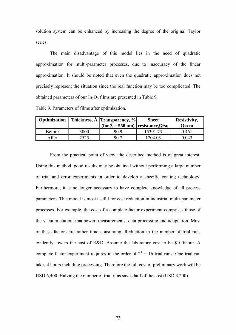
73
solution system can be enhanced by increasing the degree of the original Taylor
series.
The main disadvantage of this model lies in the need of quadratic
approximation for multi-parameter processes, due to inaccuracy of the linear
approximation. It should be noted that even the quadratic approximation does not
precisely represent the situation since the real function may be too complicated. The
obtained parameters of our In2O3 films are presented in Table 9.
Table 9. Parameters of films after optimization.
Optimization Thickness, Å Transparency, %(for λλλλ = 550 nm)
Sheet resistance,ΩΩΩΩ/sq
Resistivity, ΩΩΩΩ××××cm
Before 3000 90.9 15391.73 0.461 After 2525 90.7 1704.03 0.043
From the practical point of view, the described method is of great interest.
Using this method, good results may be obtained without performing a large number
of trial and error experiments in order to develop a specific coating technology.
Furthermore, it is no longer necessary to have complete knowledge of all process
parameters. This model is most useful for cost reduction in industrial multi-parameter
processes. For example, the cost of a complete factor experiment comprises those of
the vacuum station, manpower, measurements, data processing and adaptation. Most
of these factors are rather time consuming. Reduction in the number of trial runs
evidently lowers the cost of R&D. Assume the laboratory cost to be $100/hour. A
complete factor experiment requires in the order of 24 = 16 trial runs. One trial run
takes 4 hours including processing. Therefore the full cost of preliminary work will be
USD 6,400. Halving the number of trial runs saves half of the cost (USD 3,200).
74
3.1.2 Deposition of Ta resistive coatings with specified conductivity
3.1.2.1 Introduction.
Tantalum films were widely used as resistive coatings since the early sixties.
These films feature a negative temperature resistance coefficient (NTC),
superconductivity at low temperatures (4 K for the bulk tantalum and 40-50 K for the
tantalum oxide thin films), and a wide range of resistivity at low temperatures (10 to
1000 µΩ⋅cm at 0 to 30 % oxygen content)68. During the nineties, tantalum films were
successfully applied in microelectronic applications owing to their attractive physical
properties such as high dielectric constant (~20-40), transparency in the spectrum
range of 0.4 µm to 8 µm, high durability, corrosion resistance, and excellent
mechanical protection to the layers underneath69.
All of these advantages of tantalum oxide thin films make them usable for a
wide variety of electrical and mechanical applications. Tantalum oxide films were
applied in capacitors and in MOS transistors in dynamic random access memories
(DRAM)70, 71, in MOS memory film devices70, as photosensitive materials in Braggs
gratings for optical waveguides72, and as a protection layer in photosensitive device
systems. High dielectric constant (greater than 20) and high material strength make
the tantalum oxide films a potential candidate for replacing the silicon oxide films in
integrated circuits71. Replacement of SiO2 with Ta2O5 in VLSI capacitors results in a
six-fold increase of the capacity69, owing to its higher dielectric constant. Ta2O5 films
were applied as membranes in biomedical systems73 due to their biological
compatibility with blood and other biological matters.
The deposition techniques for tantalum oxide films and their conductivity
mechanisms were studied in several reports68,69,74. In these and some other
researches75-77 the tantalum oxide films were presented as a mixture of metallic Ta

75
and insulating Ta2O5. In these papers, a non-linear dependence between the
conductivity (σ) and the inverse temperature value (1/T) was obtained. One of the
models75 presents the electrical conductivity of the Ta + Ta2O5 system as a function of
the fractional volume of tantalum particles in the tantalum oxide matrix. However, the
experiments showed the conductivity to decrease much faster than predicted by the
model. Then the authors suggested an activation model of the process, i.e. σ ∝ exp(-
∆E/T), where ∆E is the activation energy. Therefore, the non-linearity was suggested
to be the result of a combination of metallic and tunneling conductivity. Another
proposed explanation implied the excess tantalum to form donor levels along the band
gap of Ta2O5.
Hall effect measurements showed the major carriers in the Ta+Ta2O5 system to
be of positive sign76. Using this result, F.C. Livermore et al.77 showed that the
electrical conductivity mechanism consists of both types of conductivity: metallic and
tunneling. The metallic contribution to the conductivity process acts in parallel with
the activation mechanism. To explain the conductivity mechanism, the authors of this
paper77 suggested a layer model of oxygendoped tantalum. In this model the Ta
layers varied in their oxygen content. It was shown that the two-layer model explains
the TCR sign inversion with respect to the temperature increase68. It was found that
the resistivity of both layers together could be represented by a linear function whose
slope was positive or negative in accordance with the prevailing layer.
Tantalum is a refractory (high-melting) metal. Its vapor pressure reaches 10-2
Torr at its melting point, 3000 °C. The tantalum thin films are usually formed by
sputtering methods78 or by electronbeam evaporation72. Resistive tantalum films are
usually solid solutions of (Ta + Ta2O5) or (Ta + Ta2N). The type of deposition usually
used for these films is reactive sputtering.

76
In our work we tried to use the above ideas for mathematical modeling of the
magnetron sputtering. Here, we used such modeling for the deposition of thin film
resistors consisting of tantalum and its oxides. A feasibility of depositing tantalum
films with the specified resistance values controlled by variation of the technological
parameters was successfully proved.
3.1.2.2 Experimental procedure.
The experiments were done using the same laboratory magnetron sputtering
vacuum station11 (see fig. 5). The glass microscope slides of 25*75 mm2 were used as
substrates in all experimental trials. Residual gas was used as an active oxidizing
reactive agent. By the end of the process the samples were thermally treated with the
help of a novel method known as Vacuum Photothermal Processing (VPP)79, for 2
minutes, at about 250-300°C, in a vacuum of 3-5*10-5 Torr.
The following five independent technological parameters were varied in the
deposition experiments:
- V, sputtering voltage: 1.5 to 2.5 kV;
- PAr, argon pressure: 70 to 300 mTorr;
- Pres, residual air pressure: 2.5*10-5 to 7.5*10-5 Torr;
- Ts, the substrate temperature: 200 °C;
- t, deposition duration: 1.5 to 2.5 hours.
A standard four-point probe method was used for the sheet resistance
measurement. Each sample was measured in several points, and the averaged results
were used for further estimations. The surface structure of the obtained films was
studied on a computerized metallurgical microscope with optical magnification up to
×1600. Film thickness was measured on the homemade computerized micro-
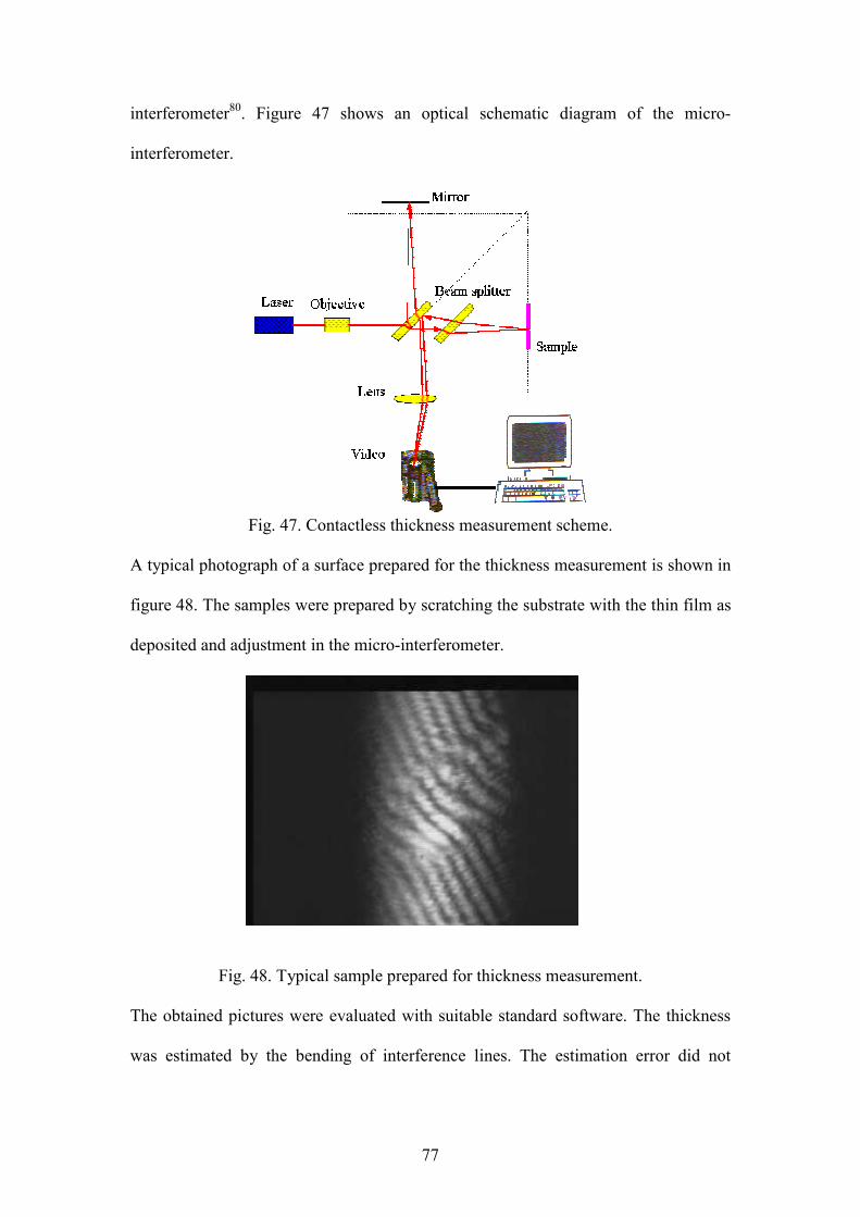
77
interferometer80. Figure 47 shows an optical schematic diagram of the micro-
interferometer.
Fig. 47. Contactless thickness measurement scheme.
A typical photograph of a surface prepared for the thickness measurement is shown in
figure 48. The samples were prepared by scratching the substrate with the thin film as
deposited and adjustment in the micro-interferometer.
Fig. 48. Typical sample prepared for thickness measurement.
The obtained pictures were evaluated with suitable standard software. The thickness
was estimated by the bending of interference lines. The estimation error did not
78
exceed 2.5%. The measurement precision was approximately 20 A°, which is no
worse than the accuracy of a standard Tenkor Instruments profilometer (100 A°).
3.1.2.3 Practical model implementation.
A magnetron sputtering process can be described in the form of the equation F
= f(x1,x2,..xi,..xn), where xi are the process parameters. The process analysis enables
us to use only several parameters, while taking other parameters as insignificant. For
the first level approximation, we chose the following equation
F = f (Pres, PAr, V, Ts, t), (95)
where Pres is the residual pressure in the vacuum chamber, PAr the working argon
pressure, V the sputtering voltage, Ts the substrate temperature, and t the
deposition duration.
In order to provide complete evaporation of the air and water molecules from the
substrate, we chose Ts = 200 °C for all the experimental trials. This temperature was
not essential for the metal film growth81, but enabled better adhesion to the substrate.
The deposition duration was two hours. With sufficiently thick tantalum layers, we
can neglect the initial stage of film growth. The long deposition duration also allows
us to neglect the influence of the residual pressure, due to a relatively high pressure of
argon gas in the course of the 2-hour process.
Therefore, for such a deposition process the following approximation model can be
applied:
σ = f(PAr, V) (96)
Here the conductivity σ represents a response function of two variables. Suppose that
the response function is analytical, so that it can be expanded in a Taylor series82. The
first three terms represent a classical second-degree equation. Therefore, the resulting
equation can be written as:
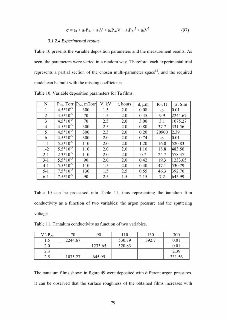
79
σ = a1 + a2PAr + a3V + a4PArV + a5PAr2 + a6V2 (97)
3.1.2.4 Experimental results.
Table 10 presents the variable deposition parameters and the measurement results. As
seen, the parameters were varied in a random way. Therefore, each experimental trial
represents a partial section of the chosen multi-parameter space82, and the required
model can be built with the missing coefficients.
Table 10. Variable deposition parameters for Ta films.
N Pres, Torr PAr, mTorr V, kV t, hours d, µm RZ, Ω σ, Sim 1 4.5*10-5 300 1.5 2.0 0.08 ∞ 0.01 2 4.5*10-5 70 1.5 2.0 0.45 9.9 2244.67 3 4.5*10-5 70 2.5 2.0 3.00 3.1 1075.27 4 4.5*10-5 300 2.5 2.0 0.80 37.7 331.56 5 4.5*10-5 300 2.3 2.0 0.20 20900 2.39 6 4.5*10-5 300 2.0 2.0 0.74 ∞ 0.01
1-1 5.5*10-5 110 2.0 2.0 1.20 16.0 520.83 1-2 5.5*10-5 110 2.0 2.0 1.10 18.8 483.56 2-1 2.3*10-5 110 2.0 2.0 0.7 24.7 578.37 3-1 5.5*10-5 90 2.0 2.0 0.42 19.3 1233.65 4-1 5.5*10-5 110 1.5 2.0 0.40 47.1 530.79 5-1 7.5*10-5 130 1.5 2.5 0.55 46.3 392.70 6-1 7.5*10-5 90 2.5 1.5 2.15 7.2 645.99
Table 10 can be processed into Table 11, thus representing the tantalum film
conductivity as a function of two variables: the argon pressure and the sputtering
voltage.
Table 11. Tantalum conductivity as function of two variables.
V \ PAr 70 90 110 130 300 1.5 2244.67 530.79 392.7 0.01 2.0 1233.65 520.83 0.01 2.3 2.39 2.5 1075.27 645.99 331.56
The tantalum films shown in figure 49 were deposited with different argon pressures.
It can be observed that the surface roughness of the obtained films increases with

80
higher pressures. The surface roughness usually reflects the presence of spot defects
or second phase inclusions. It is reasonable to assume that these defects are crystal
inclusions of the tantalum oxide film in the metal tantalum matrix. Therefore, when
the number of these inclusions (spot defects) exceeds the defined threshold level, the
activation type of conductivity become prevailing over the metallic type.
(a) (b)
© (d)
Fig. 49. Tantalum thin films photographs (X 160):
a Ar pressure of 90 mTorr, b Ar pressure of 110 mTorr,
c Ar pressure of 130 mTorr, d Ar pressure of 300 mTorr
This reasoning originates from figure 50, which represents in a graphical form the
dependence of conductivity on the working pressure, for various sputtering voltages.
It is easily observed that the graphs σ = f (PAr) are similar to each other for various
sputtering voltages. As shown in these graphs, conductivity decreases with the
increase in the working pressure. The area on the graph with a sharp bending, in
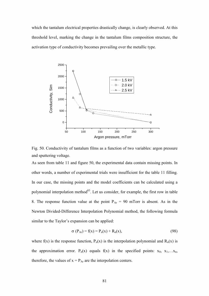
81
which the tantalum electrical properties drastically change, is clearly observed. At this
threshold level, marking the change in the tantalum films composition structure, the
activation type of conductivity becomes prevailing over the metallic type.
Fig. 50. Conductivity of tantalum films as a function of two variables: argon pressure
and sputtering voltage.
As seen from table 11 and figure 50, the experimental data contain missing points. In
other words, a number of experimental trials were insufficient for the table 11 filling.
In our case, the missing points and the model coefficients can be calculated using a
polynomial interpolation method83. Let us consider, for example, the first row in table
8. The response function value at the point PAr = 90 mTorr is absent. As in the
Newton Divided-Difference Interpolation Polynomial method, the following formula
similar to the Taylors expansion can be applied:
σ (PAr) = f(x) = Pn(x) + Rn(x), (98)
where f(x) is the response function, Pn(x) is the interpolation polynomial and Rn(x) is
the approximation error. Pn(x) equals f(x) in the specified points: x0, x1,xn,
therefore, the values of x = PAr are the interpolation centers.
50 100 150 200 250 300
0
500
1000
1500
2000
2500
1.5 kV 2.0 kV 2.5 kV
Con
duct
ivity
, Sim
Argon pressure, mTorr
82
The 3rd degree interpolation polynomial, in our case, can be written in the form of:
Pn(x) = f[x0] + (x - x0)f[x1,x0] + (x - x0)(x - x1)f[x2,x1,x0] + (99)
+ (x - x0)(x - x1)(x - x2)f[x3,x2,x1,x0]
where
This model can be re-written in the Lagrange form, for higher levels of interpolation.
Thus, the coefficients of the process model can be calculated from the following
formula:
Estimation of the required coefficients gives the following specific model:
P3(x) = -2.55*10-3x3 + 1.39x2 250.81x + 14216 (102)
Figure 51 represents this P3(x) ≈ σ(PAr) for the sputtering voltage of V = 1.5 kV.
( ) (101) )xx(
)xx()x(f
xPn
0in
ij0j
ji
n
ij0j
ji
n ∑∏
∏
=
≠=
≠=
−
−
=
(100) )xx(
)x(f)xx()xx(
)x(f...
)xx()xx()x(f
)xx()xx()x(f
)x,...,x,x(f
n
0in
ij0j
ji
i
0n1nn
0
0n1nn
1n
0n1nn
n01nn
∑∏=
≠=
−
−
−
−−
−=
−⋅⋅⋅−++
+−⋅⋅⋅−
+−⋅⋅⋅−
=

83
50 100 150 200 250 300
0
500
1000
1500
2000
2500
Data calculated by interpolationfor x = 90: y = 1044
Sputtering voltage V = 1.5 kV
Con
duci
vity
, Sim
Argon pressure, mTorr
Fig. 51. Tantalum film conductivity, calculated value.
As shown, the estimated point fits the experimental graph without disfiguring it.
Generalizing the interpolation model in 3-D84 using the Lagrange form yields the
response surface shown in figure 52.
Fig. 52. 3-D presentation of tantalum films conductivity as a function of technological
parameters.
84
This graph enables the deposition of tantalum films with pre-defined conductivity in
the chosen areas of the technological parameter variations. Thus, we have
demonstrated the possibility to successfully apply the proposed engineering method to
experiment planning and development of various deposition technologies.
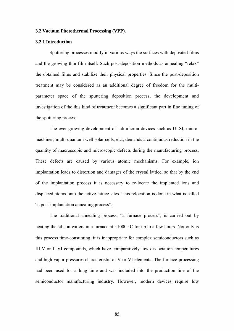
85
3.2 Vacuum Photothermal Processing (VPP).
3.2.1 Introduction
Sputtering processes modify in various ways the surfaces with deposited films
and the growing thin film itself. Such post-deposition methods as annealing relax
the obtained films and stabilize their physical properties. Since the post-deposition
treatment may be considered as an additional degree of freedom for the multi-
parameter space of the sputtering deposition process, the development and
investigation of the this kind of treatment becomes a significant part in fine tuning of
the sputtering process.
The ever-growing development of sub-micron devices such as ULSI, micro-
machines, multi-quantum well solar cells, etc., demands a continuous reduction in the
quantity of macroscopic and microscopic defects during the manufacturing process.
These defects are caused by various atomic mechanisms. For example, ion
implantation leads to distortion and damages of the crystal lattice, so that by the end
of the implantation process it is necessary to re-locate the implanted ions and
displaced atoms onto the active lattice sites. This relocation is done in what is called
a post-implantation annealing process.
The traditional annealing process, a furnace process, is carried out by
heating the silicon wafers in a furnace at ~1000 °C for up to a few hours. Not only is
this process time-consuming, it is inappropriate for complex semiconductors such as
III-V or II-VI compounds, which have comparatively low dissociation temperatures
and high vapor pressures characteristic of V or VI elements. The furnace processing
had been used for a long time and was included into the production line of the
semiconductor manufacturing industry. However, modern devices require low
86
temperature processing, low thermal and residual stress, low defect concentration, and
faster processes with high yields and throughputs.
The fundamental disadvantages of furnace processes had been overcome with
the introduction of Rapid Thermal Annealing (RTA). The first RTA process was
demonstrated in 1975 by using pulsed lasers to anneal ion implanted GaAs devices85.
Many different types of RTA methods for transient annealing were proposed since
then, although the first industrial RTA application was described in 1980 86,87. All of
these methods were based on the application of different types of heating lamps or
lasers on the annealed substrate. Further we demonstrate the experimental results of a
novel approach called Vacuum Photothermal Processing (VPP) based on fast direct
irradiation of thin films in vacuum. This approach is based on the RTA process and
relates the changes in the electric properties of the semiconductor films to photonic
rather than to thermal effects.
3.2.2 Development and investigation of VPP treatment.
3.2.2.1 Basic Principles of Rapid Thermal Processing.
The basic idea behind the RTA is the exposure of semiconductor samples to a
radiation flux generated by arc or halogen lamps. A schematic diagram of this
technique is shown in figure 53. One or two banks of halogen lamps above and below
irradiate the wafer while providing nitrogen atmosphere in the reaction chamber in
order to stabilize the vapor pressure88.
Fig. 53. Typical Rapid Thermal Annealing (RTA) [88].
87
The power to the water-cooled lamps is computer controlled via a negative feedback
loop. In the old RTA configuration, a thermocouple on a calibration wafer was used
as a temperature sensor. Most of the modern RTA systems use a pyrometer for direct
measurement of the heated wafer temperature. A typical RTA processing period for
implants in GaAs is 2 to 10 seconds in the temperature range of 800 to 1050° C.
Modifications of this technique may include several numbers of lamp banks and
several numbers of lamps in the bank. Other arrangements of the lamps structure may
also affect the final properties of the treated samples89.
The Rapid Thermal Processing (RTP) is based on incoherent radiation from
tungsten or halogen lamps90. This procedure combines the annealing process with
photonic influence. The furnace processes are caused by photons of infra-red range
with wavelengths longer than 0.8 µm. Irradiation of samples with short wavelength
(visible and UV ranges) photons permits to decrease the treatment period as well as
the annealing temperature of samples. In the case of the RTP the short wavelength
photons influence becomes more significant than heating waves. According to the
Plank radiation law for black bodies16, the maximum of the spectral radiation
distribution shifts to the shorter wavelengths part of the spectrum for higher radiation
intensities. The tungsten filament in the halogen lamps is heated up to about 3000° K
so that most of the RTP treatment is done by the shorter wavelength photons, that is,
those with energy ranging from the ultraviolet to the visible range. Obviously, the
influence mechanism of long wavelength photons on semiconductors differs from that
of the short wavelength photons. The authors of the fundamental paper91 showed that
owing to quantum effects, the incoherent light results in a short RTP impact, which
brings the reduction in the activation energy and the surface roughness, and the
improvement of the annealing uniformity.
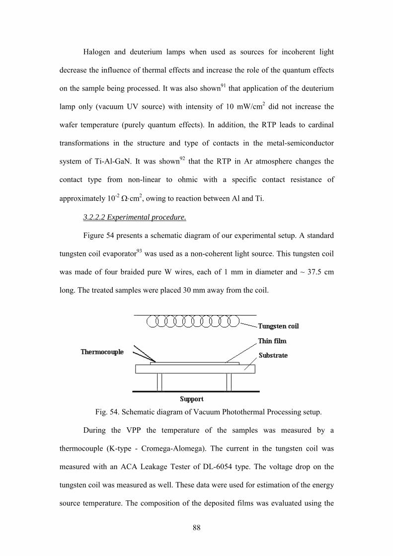
88
Halogen and deuterium lamps when used as sources for incoherent light
decrease the influence of thermal effects and increase the role of the quantum effects
on the sample being processed. It was also shown91 that application of the deuterium
lamp only (vacuum UV source) with intensity of 10 mW/cm2 did not increase the
wafer temperature (purely quantum effects). In addition, the RTP leads to cardinal
transformations in the structure and type of contacts in the metal-semiconductor
system of Ti-Al-GaN. It was shown92 that the RTP in Ar atmosphere changes the
contact type from non-linear to ohmic with a specific contact resistance of
approximately 10-2 Ω⋅cm2, owing to reaction between Al and Ti.
3.2.2.2 Experimental procedure.
Figure 54 presents a schematic diagram of our experimental setup. A standard
tungsten coil evaporator93 was used as a non-coherent light source. This tungsten coil
was made of four braided pure W wires, each of 1 mm in diameter and ~ 37.5 cm
long. The treated samples were placed 30 mm away from the coil.
Fig. 54. Schematic diagram of Vacuum Photothermal Processing setup.
During the VPP the temperature of the samples was measured by a
thermocouple (K-type - Cromega-Alomega). The current in the tungsten coil was
measured with an ACA Leakage Tester of DL-6054 type. The voltage drop on the
tungsten coil was measured as well. These data were used for estimation of the energy
source temperature. The composition of the deposited films was evaluated using the

89
Energy Dispersive Spectrometry (EDS) add-on mounted on the STEREOSCAN-430
(LEICA Scanning Electron Microscope operating on 20 keV). The film thickness was
measured with the automatic Tencor Instruments profilometer. The surface views and
structure of samples were studied on the Canon microscope with magnification up to
x1600. The fine surface roughness of the samples as deposited and after the VPP
treatment was measured with the Digital Instruments DimensionTM 3100 Scanning
Probe Microscope.
The I-V characteristics of the thin film systems prior to and after the VPP
processing were compared. In addition, the I-V characteristics of the VPP treated
samples were compared to those of the control samples. The characteristics were
obtained with the help of the Keithley bench station. Figure 55 illustrates the
measuring system.
Fig. 55. Schematic diagram of the I-V measurement.
The potential barrier between the metal electrode and the silicon was calculated from
the I-V characteristics 18, 94. The Shockley equation for the saturation current density
is:
(103)
kTq
expTAJ B2rS
Φ−=
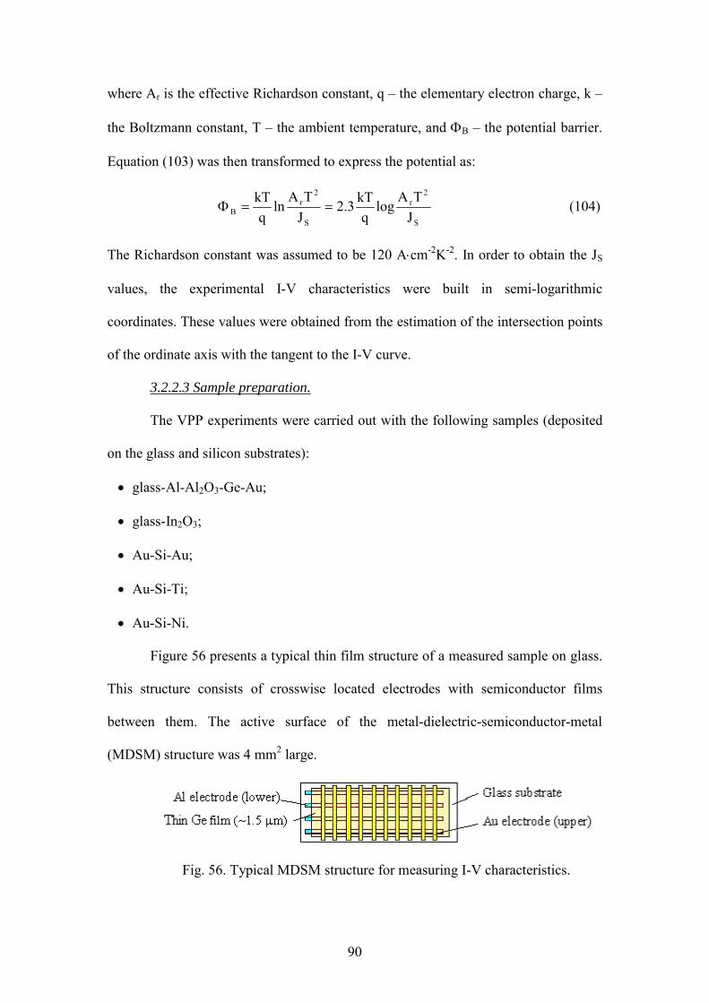
90
where Ar is the effective Richardson constant, q the elementary electron charge, k
the Boltzmann constant, T the ambient temperature, and ΦB the potential barrier.
Equation (103) was then transformed to express the potential as:
(104) JTA
logq
kT3.2JTA
lnq
kT
S
2r
S
2r
B ==Φ
The Richardson constant was assumed to be 120 A⋅cm-2K-2. In order to obtain the JS
values, the experimental I-V characteristics were built in semi-logarithmic
coordinates. These values were obtained from the estimation of the intersection points
of the ordinate axis with the tangent to the I-V curve.
3.2.2.3 Sample preparation.
The VPP experiments were carried out with the following samples (deposited
on the glass and silicon substrates):
• glass-Al-Al2O3-Ge-Au;
• glass-In2O3;
• Au-Si-Au;
• Au-Si-Ti;
• Au-Si-Ni.
Figure 56 presents a typical thin film structure of a measured sample on glass.
This structure consists of crosswise located electrodes with semiconductor films
between them. The active surface of the metal-dielectric-semiconductor-metal
(MDSM) structure was 4 mm2 large.
Fig. 56. Typical MDSM structure for measuring I-V characteristics.
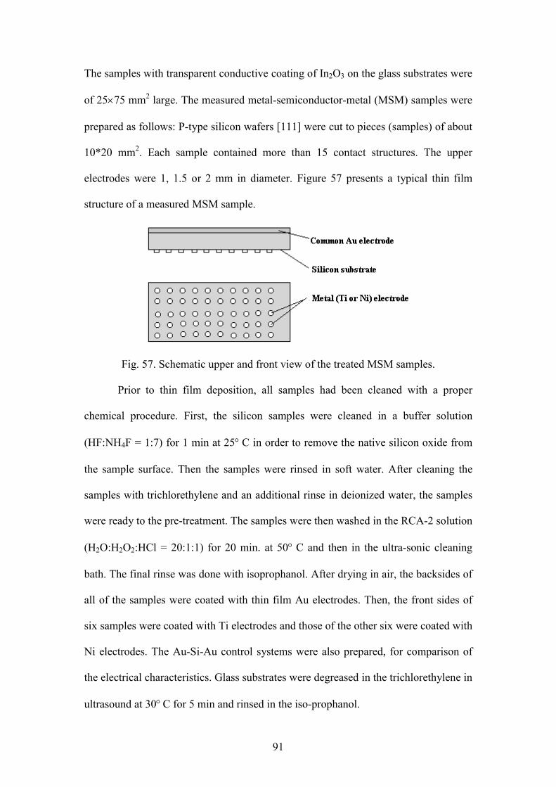
91
The samples with transparent conductive coating of In2O3 on the glass substrates were
of 25×75 mm2 large. The measured metal-semiconductor-metal (MSM) samples were
prepared as follows: P-type silicon wafers [111] were cut to pieces (samples) of about
10*20 mm2. Each sample contained more than 15 contact structures. The upper
electrodes were 1, 1.5 or 2 mm in diameter. Figure 57 presents a typical thin film
structure of a measured MSM sample.
Fig. 57. Schematic upper and front view of the treated MSM samples.
Prior to thin film deposition, all samples had been cleaned with a proper
chemical procedure. First, the silicon samples were cleaned in a buffer solution
(HF:NH4F = 1:7) for 1 min at 25° C in order to remove the native silicon oxide from
the sample surface. Then the samples were rinsed in soft water. After cleaning the
samples with trichlorethylene and an additional rinse in deionized water, the samples
were ready to the pre-treatment. The samples were then washed in the RCA-2 solution
(H2O:H2O2:HCl = 20:1:1) for 20 min. at 50° C and then in the ultra-sonic cleaning
bath. The final rinse was done with isoprophanol. After drying in air, the backsides of
all of the samples were coated with thin film Au electrodes. Then, the front sides of
six samples were coated with Ti electrodes and those of the other six were coated with
Ni electrodes. The Au-Si-Au control systems were also prepared, for comparison of
the electrical characteristics. Glass substrates were degreased in the trichlorethylene in
ultrasound at 30° C for 5 min and rinsed in the iso-prophanol.

92
All metal films were deposited on the laboratory evaporation vacuum setup
with the vacuum of approximately 3*10-5 Torr. The substrate temperature during
evaporation was ~200° C. A thin film of Al2O3 is a natural oxide that grows on the
lower electrode while exposing the vacuum chamber to air. The germanium thin films
and semiconductor indium oxide thin films were grown by sputtering using a
laboratory magnetron vacuum station95, 96. The grown Ge films were about 1.5 µm
thick. The thickness of the In2O3 transparent conductive thin films was found to be
about 250 nm82.
3.2.2.4 Control experiments.
It was found that the temperature of the samples during the VPP raises up to
about 400° C (see figure 58).
Fig. 58. Typical Vacuum Photothermal Processing.
Our goal in this work was to verify the type of the treatment mechanism. There are
several factors of influence on the VPP: ultra-violet photons, thermal effects, and
electrons emitted from the heated tungsten wire. The examination was done in three
ways. In the first control experiment, the similar samples were heated up by a hot
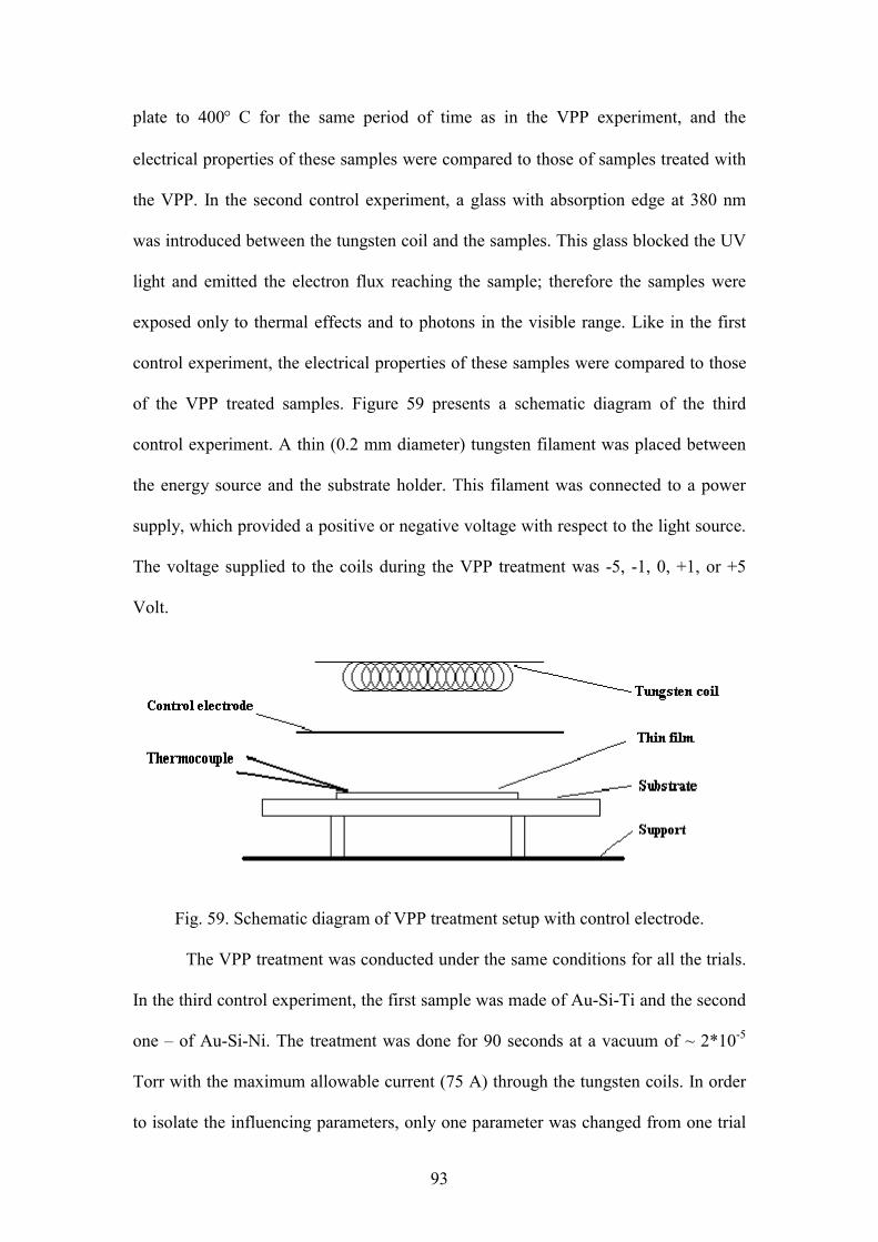
93
plate to 400° C for the same period of time as in the VPP experiment, and the
electrical properties of these samples were compared to those of samples treated with
the VPP. In the second control experiment, a glass with absorption edge at 380 nm
was introduced between the tungsten coil and the samples. This glass blocked the UV
light and emitted the electron flux reaching the sample; therefore the samples were
exposed only to thermal effects and to photons in the visible range. Like in the first
control experiment, the electrical properties of these samples were compared to those
of the VPP treated samples. Figure 59 presents a schematic diagram of the third
control experiment. A thin (0.2 mm diameter) tungsten filament was placed between
the energy source and the substrate holder. This filament was connected to a power
supply, which provided a positive or negative voltage with respect to the light source.
The voltage supplied to the coils during the VPP treatment was -5, -1, 0, +1, or +5
Volt.
Fig. 59. Schematic diagram of VPP treatment setup with control electrode.
The VPP treatment was conducted under the same conditions for all the trials.
In the third control experiment, the first sample was made of Au-Si-Ti and the second
one of Au-Si-Ni. The treatment was done for 90 seconds at a vacuum of ~ 2*10-5
Torr with the maximum allowable current (75 A) through the tungsten coils. In order
to isolate the influencing parameters, only one parameter was changed from one trial
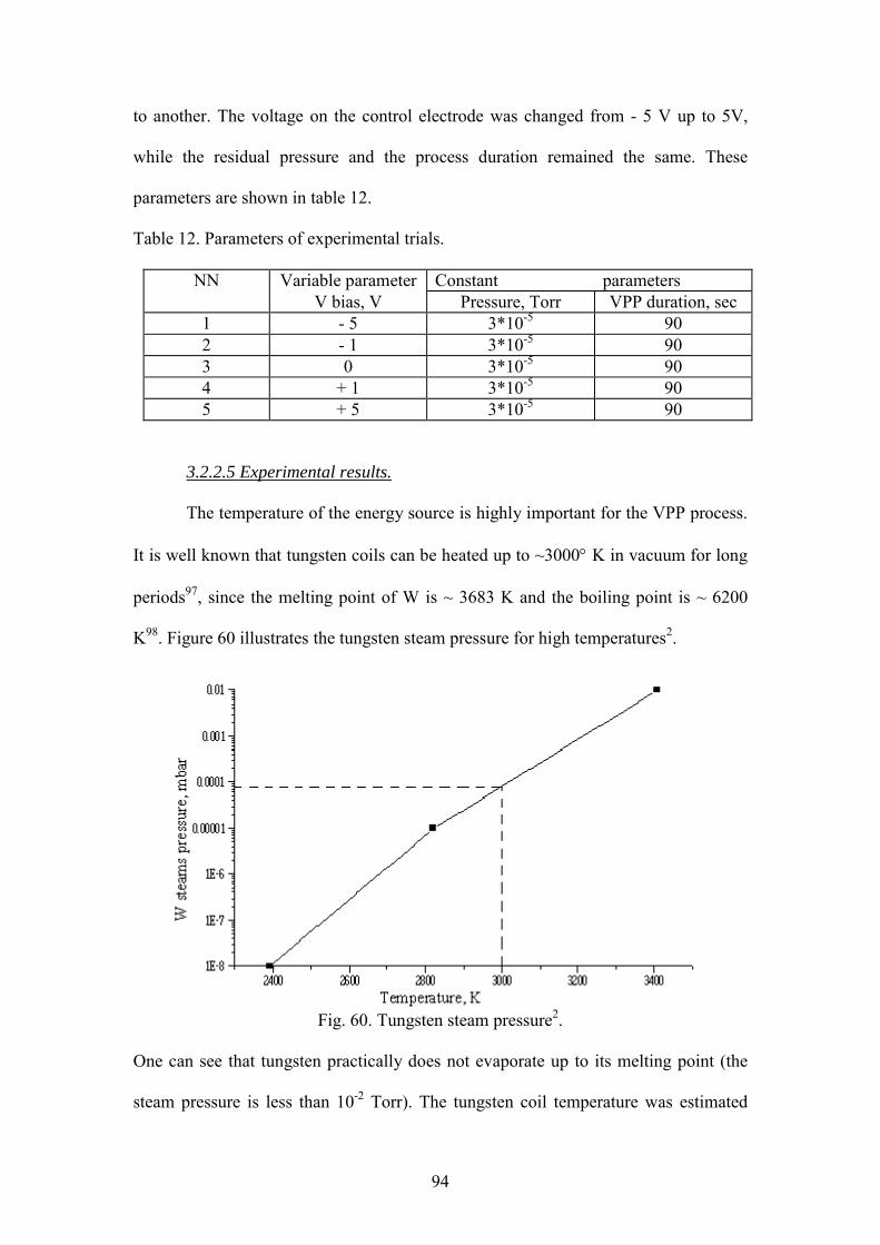
94
to another. The voltage on the control electrode was changed from - 5 V up to 5V,
while the residual pressure and the process duration remained the same. These
parameters are shown in table 12.
Table 12. Parameters of experimental trials.
NN Variable parameter Constant parameters V bias, V Pressure, Torr VPP duration, sec 1 - 5 3*10-5 90 2 - 1 3*10-5 90 3 0 3*10-5 90 4 + 1 3*10-5 90 5 + 5 3*10-5 90
3.2.2.5 Experimental results.
The temperature of the energy source is highly important for the VPP process.
It is well known that tungsten coils can be heated up to ~3000° K in vacuum for long
periods97, since the melting point of W is ~ 3683 K and the boiling point is ~ 6200
K98. Figure 60 illustrates the tungsten steam pressure for high temperatures2.
Fig. 60. Tungsten steam pressure2.
One can see that tungsten practically does not evaporate up to its melting point (the
steam pressure is less than 10-2 Torr). The tungsten coil temperature was estimated
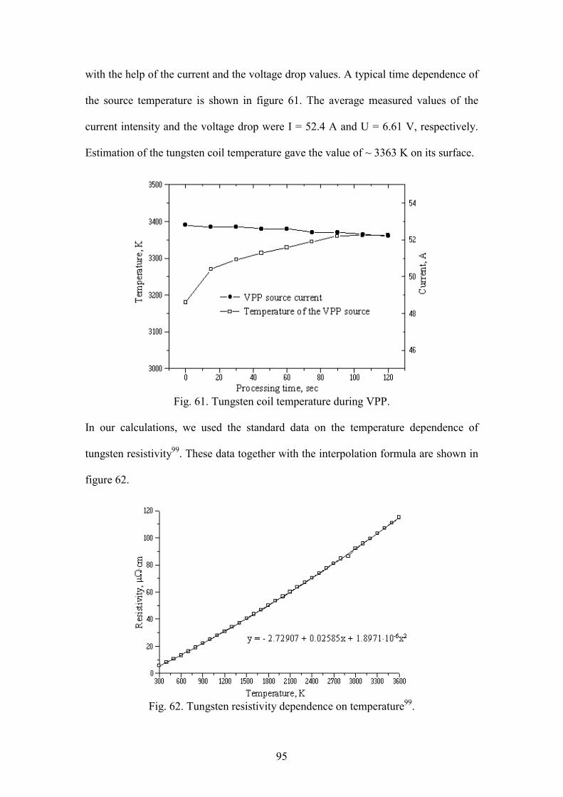
95
with the help of the current and the voltage drop values. A typical time dependence of
the source temperature is shown in figure 61. The average measured values of the
current intensity and the voltage drop were I = 52.4 A and U = 6.61 V, respectively.
Estimation of the tungsten coil temperature gave the value of ~ 3363 K on its surface.
Fig. 61. Tungsten coil temperature during VPP.
In our calculations, we used the standard data on the temperature dependence of
tungsten resistivity99. These data together with the interpolation formula are shown in
figure 62.
Fig. 62. Tungsten resistivity dependence on temperature99.
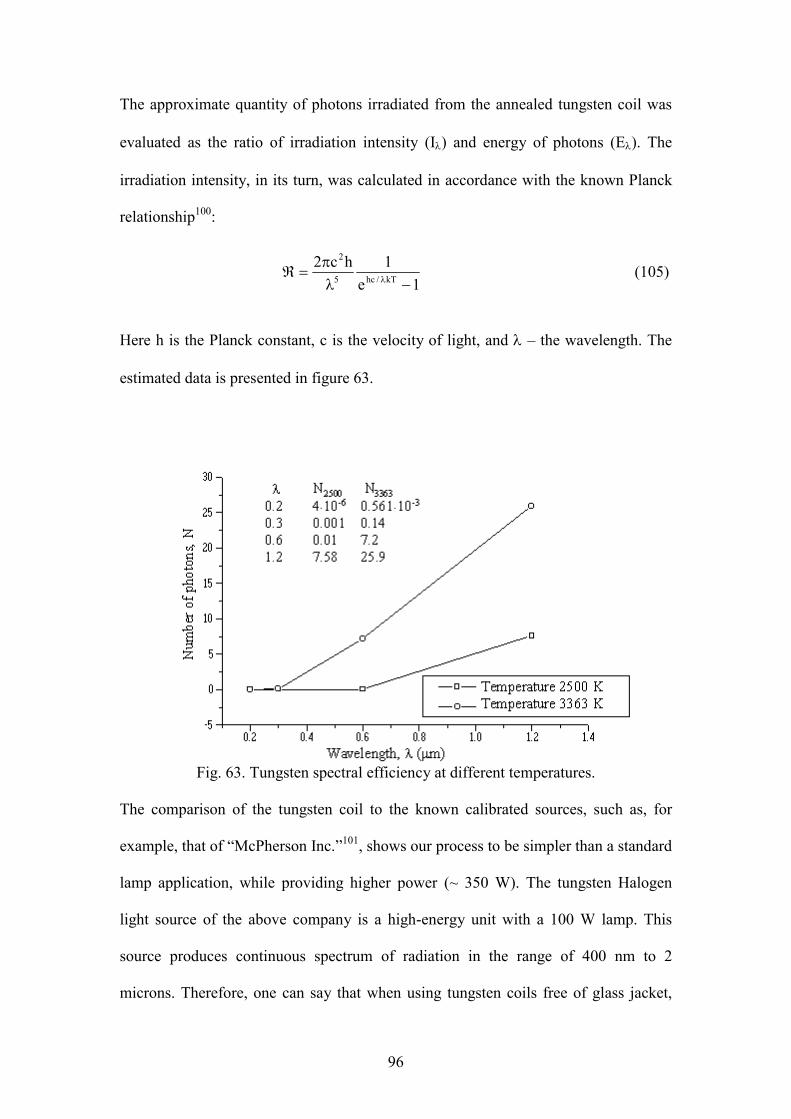
96
The approximate quantity of photons irradiated from the annealed tungsten coil was
evaluated as the ratio of irradiation intensity (Iλ) and energy of photons (Eλ). The
irradiation intensity, in its turn, was calculated in accordance with the known Planck
relationship100:
Here h is the Planck constant, c is the velocity of light, and λ the wavelength. The
estimated data is presented in figure 63.
Fig. 63. Tungsten spectral efficiency at different temperatures.
The comparison of the tungsten coil to the known calibrated sources, such as, for
example, that of McPherson Inc.101, shows our process to be simpler than a standard
lamp application, while providing higher power (~ 350 W). The tungsten Halogen
light source of the above company is a high-energy unit with a 100 W lamp. This
source produces continuous spectrum of radiation in the range of 400 nm to 2
microns. Therefore, one can say that when using tungsten coils free of glass jacket,
(105) 1e
1hc2kT/hc5
2
−λπ
=ℜ λ
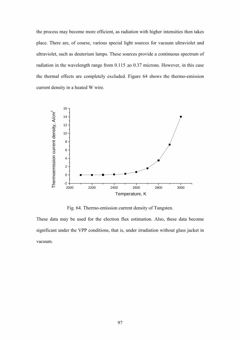
97
the process may become more efficient, as radiation with higher intensities then takes
place. There are, of course, various special light sources for vacuum ultraviolet and
ultraviolet, such as deuterium lamps. These sources provide a continuous spectrum of
radiation in the wavelength range from 0.115 до 0.37 microns. However, in this case
the thermal effects are completely excluded. Figure 64 shows the thermo-emission
current density in a heated W wire.
Fig. 64. Thermo-emission current density of Tungsten.
These data may be used for the electron flux estimation. Also, these data become
significant under the VPP conditions, that is, under irradiation without glass jacket in
vacuum.
2000 2200 2400 2600 2800 3000-2
0
2
4
6
8
10
12
14
16
Ther
moe
mis
sion
cur
rent
den
sity
, A/c
m2
Temperature, K
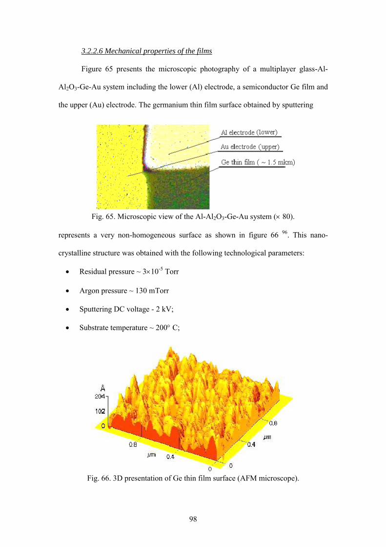
98
3.2.2.6 Mechanical properties of the films
Figure 65 presents the microscopic photography of a multiplayer glass-Al-
Al2O3-Ge-Au system including the lower (Al) electrode, a semiconductor Ge film and
the upper (Au) electrode. The germanium thin film surface obtained by sputtering
Fig. 65. Microscopic view of the Al-Al2O3-Ge-Au system (× 80).
represents a very non-homogeneous surface as shown in figure 66 96. This nano-
crystalline structure was obtained with the following technological parameters:
• Residual pressure ~ 3×10⁻⁵ Torr
• Argon pressure ~ 130 mTorr
• Sputtering DC voltage - 2 kV;
• Substrate temperature ~ 200° C;
Fig. 66. 3D presentation of Ge thin film surface (AFM microscope).

99
This surface was found to have many surface states, which essentially influenced the
electron transport mobility in the studied system. A rapid thermal processing step has
been shown to be a cure mechanism to produce precise structural phase
transformations, including carrier traps removal 102,103.
The three main parameters that most influence the thin film system properties
during thermal processing are the film material and thickness, and the thermal
treatment duration. The vacuum photo-thermal processing was studied for various
processing intervals, materials and film thicknesses. The treatment period was chosen
according to the known data2, ranging from 15 to 90 seconds. The influence of the
thermal processes becomes significant after about 120 seconds of treatment due to the
temperature increase of the sample, resulting in higher diffusion rate. For
temperatures higher than 400°C, the Au atoms penetrate the semiconductor system
and the entire structure is destroyed. Figure 67 presents comparative external views of
some samples treated by the VPP and by the conventional furnace annealing
treatment.
Fig. 67. External view of the processed MDSM samples.

100
All samples designated 2b were heated up to 400°C and were destroyed in a real-time
measurement due to the different thermal expansion/contraction coefficients of the
semiconductor layers and the glass substrate. The thin films were wrecked and part of
Au atoms were diffused into the Ge layer. On the other hand, all of the VPP treated
samples (1b) kept their shape and form.
A view of the MSM samples before and after the VPP treatment is presented
in figures 68 and 69. These figures demonstrate the significant changes in the
electrode surfaces. Figures 68a and 68b show the Ni electrodes with magnification
×150 and ×3000, respectively.
(a) (b)
© (d)
Fig. 68. Experimental photographs of Ni electrodes on silicon for as deposited and
VPP treated samples, in two magnifications:
(a) as deposited film, *150; (b) as deposited film, *3000;
© VPP treated film, *150; (d) VPP treated film, *3000.
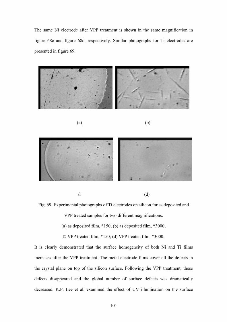
101
The same Ni electrode after VPP treatment is shown in the same magnification in
figure 68c and figure 68d, respectively. Similar photographs for Ti electrodes are
presented in figure 69.
(a) (b)
© (d)
Fig. 69. Experimental photographs of Ti electrodes on silicon for as deposited and
VPP treated samples for two different magnifications:
(a) as deposited film, *150; (b) as deposited film, *3000;
© VPP treated film, *150; (d) VPP treated film, *3000.
It is clearly demonstrated that the surface homogeneity of both Ni and Ti films
increases after the VPP treatment. The metal electrode films cover all the defects in
the crystal plane on top of the silicon surface. Following the VPP treatment, these
defects disappeared and the global number of surface defects was dramatically
decreased. K.P. Lee et al. examined the effect of UV illumination on the surface
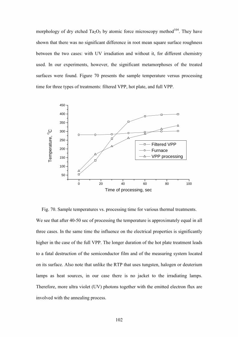
102
morphology of dry etched Ta2O5 by atomic force microscopy method104. They have
shown that there was no significant difference in root mean square surface roughness
between the two cases: with UV irradiation and without it, for different chemistry
used. In our experiments, however, the significant metamorphoses of the treated
surfaces were found. Figure 70 presents the sample temperature versus processing
time for three types of treatments: filtered VPP, hot plate, and full VPP.
0 20 40 60 80 100
50
100
150
200
250
300
350
400
450
Filtered VPP Furnace VPP processing
Tem
pera
ture
, OC
Time of processing, sec
Fig. 70. Sample temperatures vs. processing time for various thermal treatments.
We see that after 40-50 sec of processing the temperature is approximately equal in all
three cases. In the same time the influence on the electrical properties is significantly
higher in the case of the full VPP. The longer duration of the hot plate treatment leads
to a fatal destruction of the semiconductor film and of the measuring system located
on its surface. Also note that unlike the RTP that uses tungsten, halogen or deuterium
lamps as heat sources, in our case there is no jacket to the irradiating lamps.
Therefore, more ultra violet (UV) photons together with the emitted electron flux are
involved with the annealing process.

103
The 3D atomic force microscope (AFM) pictures of these treated Ti films are
presented in figure 71. Comparison between figures 71a and 71b emphasizes the
smoothing effect of the VPP treatment. The second picture presents the flat plane
surface of the metal electrode. Following the VPP treatment the metallic grains
became lower and the roughness decreased. The AFM section analysis of the
roughness is shown in figure 72. It can be seen that the mean roughness on the VPP
treated samples decreases to less than a half and the maximum surface grain height
decreases from 6.67 nm to 1.83 nm.
(a) (b)
Fig. 71. 3D AFM photographs of as deposited and VPP treated Ti films.
(a) as deposited Au-Si-Ti system; (b) VPP treated Au-Si-Ti system.
(a) (b)
Fig. 72. AFM section analysis of roughness for as deposited and VPP treated Au-Si-
Ti systems.
(a) (a) as deposited Au-Si-Ti system; (b) VPP treated Au-Si-Ti system.
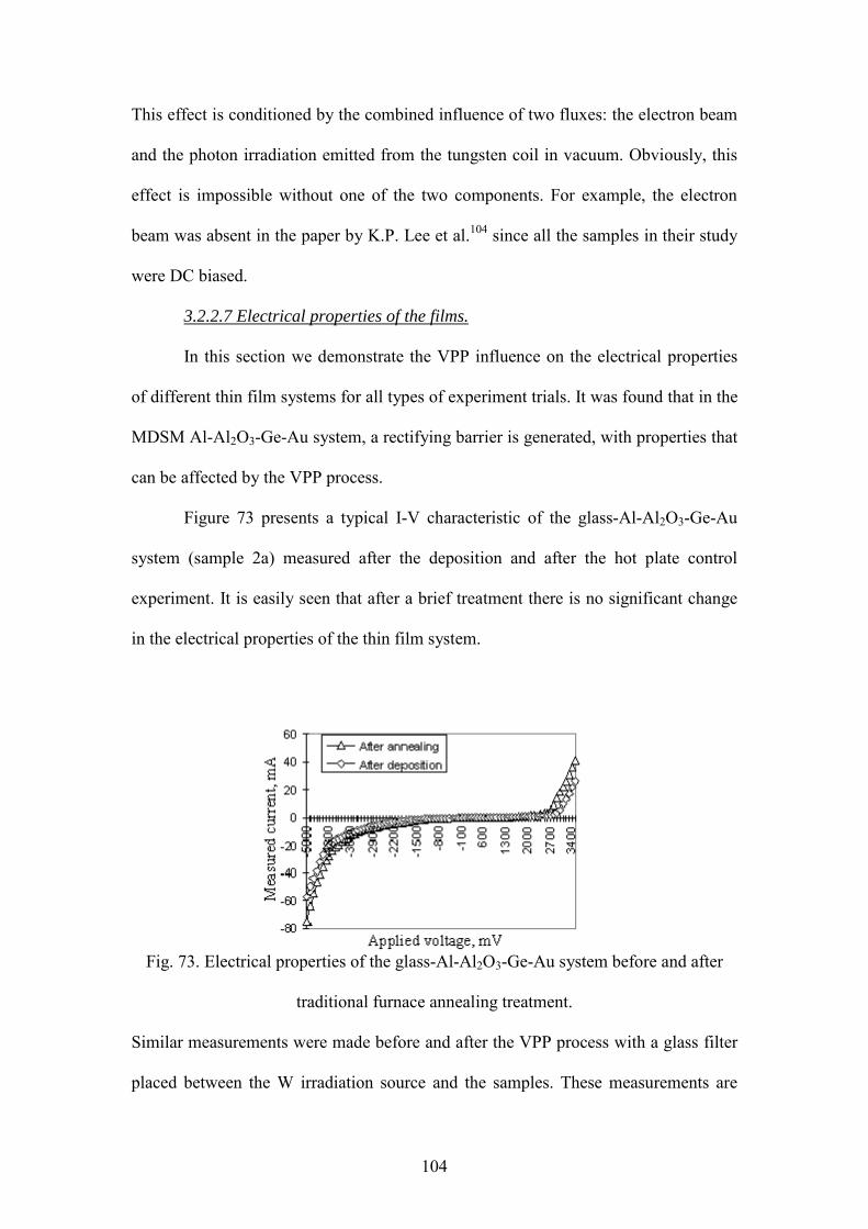
104
This effect is conditioned by the combined influence of two fluxes: the electron beam
and the photon irradiation emitted from the tungsten coil in vacuum. Obviously, this
effect is impossible without one of the two components. For example, the electron
beam was absent in the paper by K.P. Lee et al.104 since all the samples in their study
were DC biased.
3.2.2.7 Electrical properties of the films.
In this section we demonstrate the VPP influence on the electrical properties
of different thin film systems for all types of experiment trials. It was found that in the
MDSM Al-Al2O3-Ge-Au system, a rectifying barrier is generated, with properties that
can be affected by the VPP process.
Figure 73 presents a typical I-V characteristic of the glass-Al-Al2O3-Ge-Au
system (sample 2a) measured after the deposition and after the hot plate control
experiment. It is easily seen that after a brief treatment there is no significant change
in the electrical properties of the thin film system.
Fig. 73. Electrical properties of the glass-Al-Al2O3-Ge-Au system before and after
traditional furnace annealing treatment.
Similar measurements were made before and after the VPP process with a glass filter
placed between the W irradiation source and the samples. These measurements are

105
shown in figure 74. The most significant modifications in the electrical properties (as
compared to the hot plate control experiment) are mainly due to the added W coil
irradiation in the visible range.
Fig. 74. VPP with glass filter (sample 1b).
Figure 75 shows the I-V characteristics before and after a VPP process. The
experiment was done on several typical glass-Al-Al2O3-Ge-Au samples (1A). All
samples were grown under the same conditions, and the resulting Ge layer was about
~1.5 µm thick for all the samples. We conclude from these results that the factors
responsible for essential modification in the film properties are shorter wavelength
irradiation together with the electron flux emitted by the W coil during the VPP.
Fig. 75. VPP processing of a glass-Al-Al2O3-Ge-Au system.

106
In this figure, the VPP results in an increase of the thin film resistance and of
the built-in potential barrier height. This phenomenon can be explained by excitation
of free bonds in the boundary between the metal and the nano-crystalline germanium
layers owing to the absorbed short-wavelength photons. On the other hand, the
excited surface states are saturated, and the potential barrier increases. In other words,
the number of free charge carriers in the semiconductor and in the interface between
the metal electrode and the semiconductor film decreases. Furthermore, after the VPP,
the breakdown points were cured and the breakdown voltage increased, which also
resulted in reduced number of free charge carriers.
As shown in figures 76 and 77, the VPP reduces the sheet resistance value in
the glass-In2O3 systems, while improving its uniformity. This effect can be explained
by the redistribution of the partially oxidized indium atoms in the oxide film and the
partial reduction of indium oxide at the expense of excited electrons under the ultra-
violet photon impact. Therefore, the VPP is found to improve the quality of
transparent conductive layers.
The sheet resistance measurements were carried out on the surfaces of the
samples by the four-point method. These measurements have shown a significant
decrease in the sheet resistance of the film, from about 1,000 Ω/Sq to an average
value of 120 Ω/Sq. The uniformity of the sheet resistance across the sample was
improved as well.
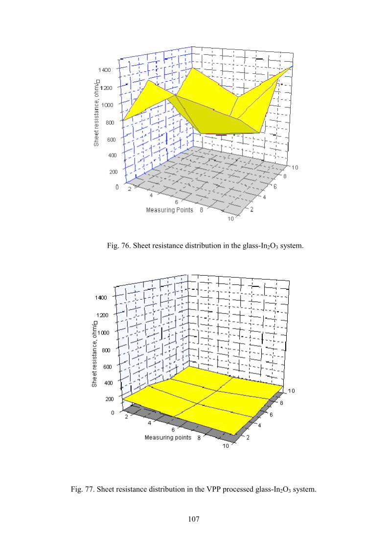
107
Fig. 76. Sheet resistance distribution in the glass-In2O3 system.
Fig. 77. Sheet resistance distribution in the VPP processed glass-In2O3 system.
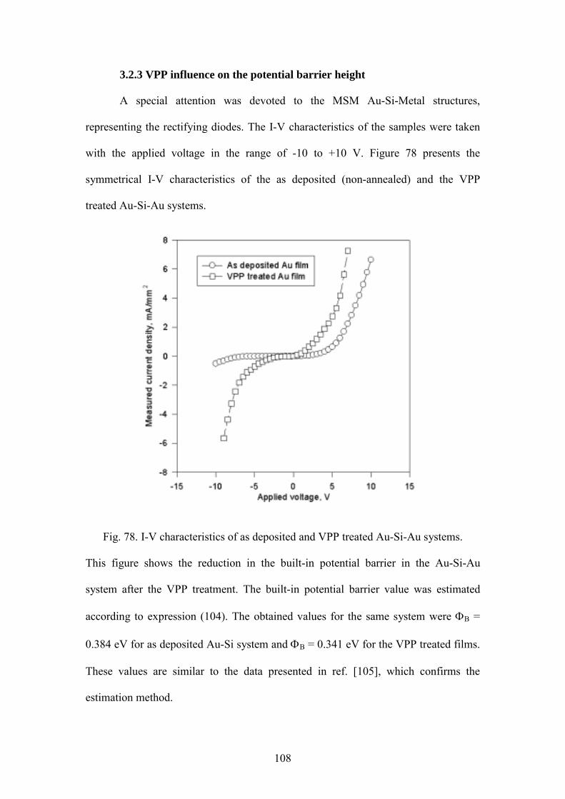
108
3.2.3 VPP influence on the potential barrier height
A special attention was devoted to the MSM Au-Si-Metal structures,
representing the rectifying diodes. The I-V characteristics of the samples were taken
with the applied voltage in the range of -10 to +10 V. Figure 78 presents the
symmetrical I-V characteristics of the as deposited (non-annealed) and the VPP
treated Au-Si-Au systems.
Fig. 78. I-V characteristics of as deposited and VPP treated Au-Si-Au systems.
This figure shows the reduction in the built-in potential barrier in the Au-Si-Au
system after the VPP treatment. The built-in potential barrier value was estimated
according to expression (104). The obtained values for the same system were ΦB =
0.384 eV for as deposited Au-Si system and ΦB = 0.341 eV for the VPP treated films.
These values are similar to the data presented in ref. [105], which confirms the
estimation method.
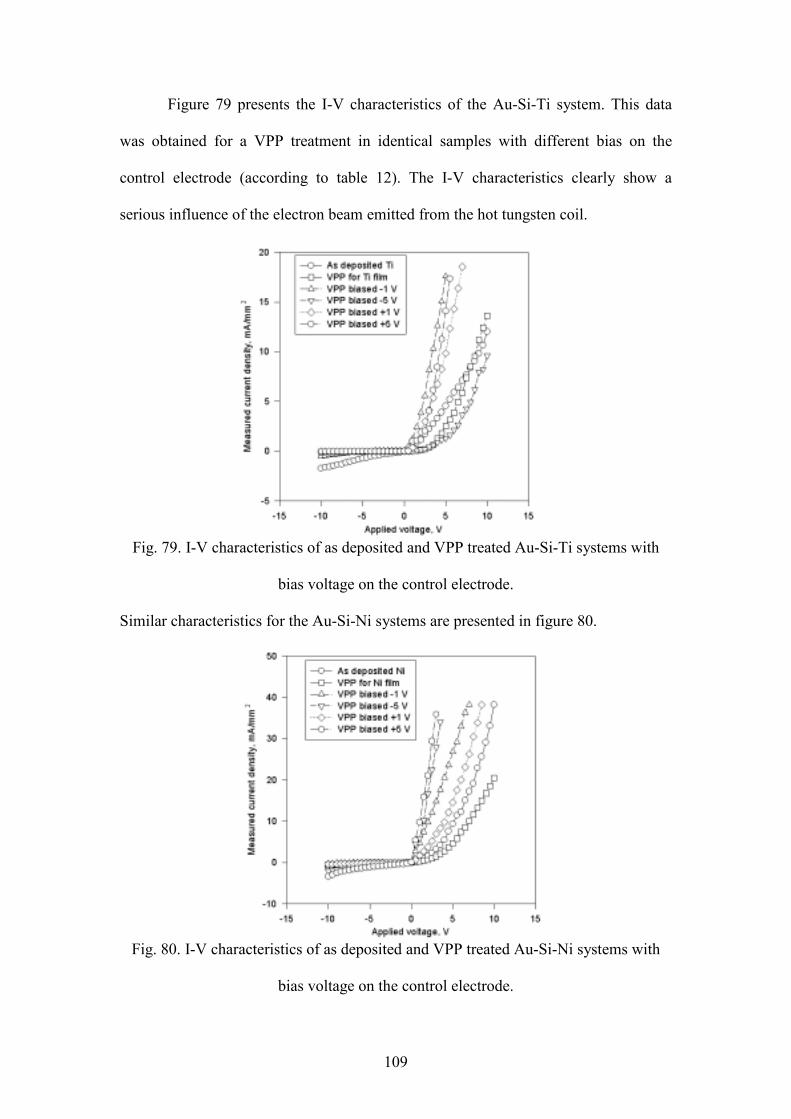
109
Figure 79 presents the I-V characteristics of the Au-Si-Ti system. This data
was obtained for a VPP treatment in identical samples with different bias on the
control electrode (according to table 12). The I-V characteristics clearly show a
serious influence of the electron beam emitted from the hot tungsten coil.
Fig. 79. I-V characteristics of as deposited and VPP treated Au-Si-Ti systems with
bias voltage on the control electrode.
Similar characteristics for the Au-Si-Ni systems are presented in figure 80.
Fig. 80. I-V characteristics of as deposited and VPP treated Au-Si-Ni systems with
bias voltage on the control electrode.
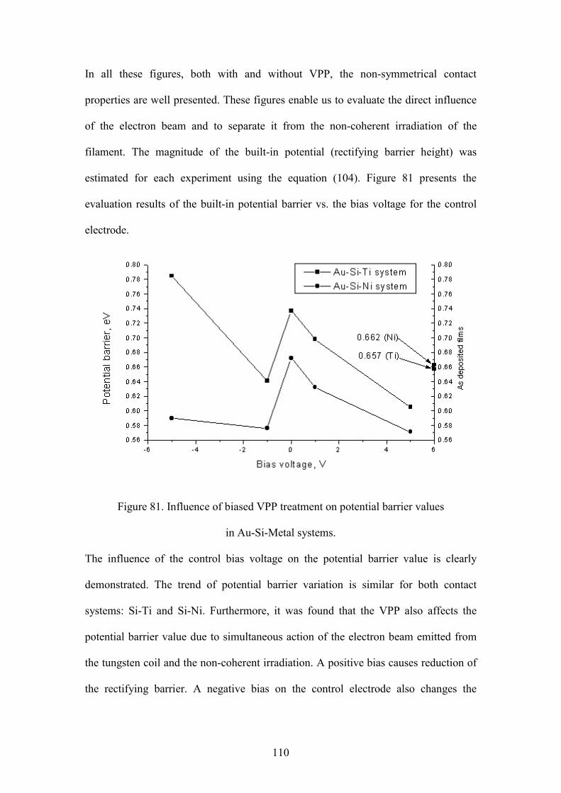
110
In all these figures, both with and without VPP, the non-symmetrical contact
properties are well presented. These figures enable us to evaluate the direct influence
of the electron beam and to separate it from the non-coherent irradiation of the
filament. The magnitude of the built-in potential (rectifying barrier height) was
estimated for each experiment using the equation (104). Figure 81 presents the
evaluation results of the built-in potential barrier vs. the bias voltage for the control
electrode.
Figure 81. Influence of biased VPP treatment on potential barrier values
in Au-Si-Metal systems.
The influence of the control bias voltage on the potential barrier value is clearly
demonstrated. The trend of potential barrier variation is similar for both contact
systems: Si-Ti and Si-Ni. Furthermore, it was found that the VPP also affects the
potential barrier value due to simultaneous action of the electron beam emitted from
the tungsten coil and the non-coherent irradiation. A positive bias causes reduction of
the rectifying barrier. A negative bias on the control electrode also changes the
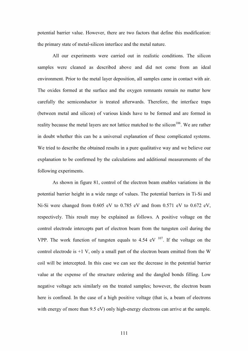
111
potential barrier value. However, there are two factors that define this modification:
the primary state of metal-silicon interface and the metal nature.
All our experiments were carried out in realistic conditions. The silicon
samples were cleaned as described above and did not come from an ideal
environment. Prior to the metal layer deposition, all samples came in contact with air.
The oxides formed at the surface and the oxygen remnants remain no matter how
carefully the semiconductor is treated afterwards. Therefore, the interface traps
(between metal and silicon) of various kinds have to be formed and are formed in
reality because the metal layers are not lattice matched to the silicon106. We are rather
in doubt whether this can be a universal explanation of these complicated systems.
We tried to describe the obtained results in a pure qualitative way and we believe our
explanation to be confirmed by the calculations and additional measurements of the
following experiments.
As shown in figure 81, control of the electron beam enables variations in the
potential barrier height in a wide range of values. The potential barriers in Ti-Si and
Ni-Si were changed from 0.605 eV to 0.785 eV and from 0.571 eV to 0.672 eV,
respectively. This result may be explained as follows. A positive voltage on the
control electrode intercepts part of electron beam from the tungsten coil during the
VPP. The work function of tungsten equals to 4.54 eV 107. If the voltage on the
control electrode is +1 V, only a small part of the electron beam emitted from the W
coil will be intercepted. In this case we can see the decrease in the potential barrier
value at the expense of the structure ordering and the dangled bonds filling. Low
negative voltage acts similarly on the treated samples; however, the electron beam
here is confined. In the case of a high positive voltage (that is, a beam of electrons
with energy of more than 9.5 eV) only high-energy electrons can arrive at the sample.

112
These electrons may penetrate through the metal electrode and result in a significant
decrease in the potential barrier. This reduction may be explained by the interface
ordering, that is, ordering of both the silicon surface defects and the metal growing
defects. As shown in figures 46 47 and 49 - 50, the roughness of samples decreased
with the controlled VPP treatment. On the contrary, using UV irradiation without
electron beam has no significant effect on the roughness of treated surfaces104. High
negative voltage acts similarly on the various metals, however, in a reverse trend to
the positive voltage. We tried to explain this fact by taking into consideration the fine
metal structure. The metals that we used in our experiments (Ti, Ni) are referred to as
transition metals108, whose upper d-shell electrons should be considered as the valence
electrons109. Nickel and titanium have two electrons in the upper orbit. However, two
electrons are missing in the upper d-shells of nickel atoms and eight electrons in
those of titanium. This difference in the energetic structure of metals explains the
difference in behavior between the VPP treated Si-Ti and Si-Ni samples. Under a high
energetic electron current beam, the Si-Ti system first fills the electron states in the
unfilled electron orbit, and only then begins to fill the external orbit. Although the
system Si-Ni behaves similarly, the number of free electron states in this system is
less than in Si-Ti. The gold atom, on the contrary, has fully complete upper d-shells.
So, in the Si-Au system, the gold atom behaves oppositely to the described VPP
treatment mechanism. In this system the potential barrier value decreases following
the VPP from 0.384 eV to 0.341 eV.
It is of interest to note a similar behavior of Ti and Ni metals under the
influence of the light and electron beam irradiation during the VPP, as shown in
figure 81. We believe this behavior to be specified by the common metal properties of
these elements. The difference between them is determined by the different number of

113
electrons in the upper d-shell. We also suppose the similar behavior of other metals
with similar structures, which fact it will be of interest to study experimentally.

114
4. CONCLUSIONS AND FUTURE DIRECTIONS
4.1 Conclusions.
Vacuum deposition methods are very important to the up-to-date
microelectronics technology. Sputtering is one of the most useful methods for thin
film deposition. In the present work we have demonstrated a novel sputtering
deposition method and the apparatus for its implementation. The basic idea derives
from a mathematical approach describing a complex system as multi-parametric with
several levels of freedom. Each independent parameter should be considered as a
level of freedom. Such approach enables a fine control of the deposition process. In
our work, we have achieved the following results:
1. An artificial plane plasma discharge was obtained in a comparatively high
vacuum; a special construction for moving the plane plasma was implemented and
tested.
2. Electron temperature and ion concentration distribution in the plane plasma was
studied with the help of Langmuir probe measurement.
3. A novel multiparameter sputtering deposition system based on the plane plasma
discharge was developed.
4. The novel sputtering system enables the deposition of metal and semiconductor
thin films in high vacuum (0.2 - 5 mTorr) with high and fine-controllable
deposition rates (Si and Ti films were deposited and tested).
5. In this deposition system, the substrate is totally isolated from the plasma; the
substrate temperature is not affected by the plasma.
6. The target material sputters homogeneously over the entire target surface (in
contrast to the magnetron sputtering); an additional support electrode confines the
sputtering ions and decreases the loss of sputtered atoms.
115
7. A modeling method for the deposition processes based on the theory of
multiparameter systems was developed; the method of partial sections in a
multiparameter space was applied for decreasing the number of trial-and-error
attempts in the course of development of a specific deposition technology.
8. This modeling method was used for the development of practical sputtering
deposition technologies for specific materials, such as transparent conductive
In2O3 films and Ta resistors with predefined resistivity.
9. A novel method, the Vacuum Photo-Thermal Processing (VPP), for heat treatment
of deposited films, was developed. This method can be considered as an additional
level of freedom in the multiparameter system. The VPP consists of a
simultaneous irradiation of the treated sample in vacuum with electron flux and
non-coherent light, mainly from the UV and VUV spectrum.
10. The VPP provides for stabilizing the deposited coatings, improved homogeneity,
and curing the irreversible electrical breakdown in thin-film systems; it also
decreases the number of surface states and improves the roughness of surfaces and
interfaces between the semiconductor and the metal film coating.
11. A method for controlling the electron flux during VPP was developed. It was
found that the value of the electron flux affects the potential barrier height in the
rectifying diodes. The possibility of operating the potential barrier height in the
metal-silicon contact systems was studied.
12. It was found that the potential barriers for the pairs Si Ti and Si Ni behave in
the same way and the physical changes on the interface are identical in nature.

116
4.2 Future Directions.
In extension of our investigations in the field of the plane plasma discharge, it
seems important to study the electron temperature distribution more precisely when
implementing this plasma for reactive sputtering deposition. This application should
extend the DC sputtering for deposition of dielectric films and various semiconductor
films. We also suggest to use the proposed sputtering method for the case of complex
intermetallic compounds such as NiCr and YBa2CuO3. A high RF voltage applied to
the target support electrode pair will enable direct sputtering of dielectric materials.
Since the sputtering in our experiments was carried out in a comparatively high
vacuum (collisionless case), we believe that the deposited films will be of
stoichiometric composition. We believe that the novel sputtering method
demonstrated in our work can be used for numerous types of materials and
applications.
In this work we developed a novel type of thermal post-deposition treatment
(VPP). At present, only the effect of the VPP on the Ti and Ni has been studied. We
are also planning to study the VPP influence on other metals, as well as on the
interfaces of metals with a number of semiconductors, to begin with Ge and SiC.
Moreover, it seems highly important to investigate the specific nature of VPP
influence on the metal-semiconductor interface in order to find whether the VPP can
be used for repair of neutron-irradiated semiconductor devices. The physics and
chemistry of VPP and participation of hydroxyl groups, hydrogen, and water
molecules in these process also will be subject of future works.
117
REFERENCES
1. S Ismat Shah, Handbook of Thin Film Process technology, IOP Publishing Ltd.,
1995.
2. L.I. Maissel, R. Glang, Handbook of Thin Film Technology, McGraw-Hill,
N.Y., 1970.
3. A. Wynveen, Fan, J., Kakalios, J., Shinar, J., Studies of light soaking stability in
rf sputter-deposited a-Si:H,
http://cmp.ameslab.gov/cmp/Abstracts/shinar_21.html
4. M.A. Lieberman, A.J. Lichtenberg, Principles of plasma discharges and materials
processing, John Wiley & Sons, Inc, N.Y., 1994.
5. S. Minomura, Metallic modified material of intermetallic compound, Pat. USA
N 4238232,1980.
6. R. Kossowsky, Surface Modification Engineering, CRC Press, Boca Raton,
1989.
7. N. St. J. Braithwaite, Introduction to gas discharge, Plasma Source Sci. Technol.
9 (2000) 517 527.
8. T. Mousel, W. Eckstein, H. Gnaser, Energy spectra of sputtered species under
sub-keV ion bombardment: experiments and computer simulations, Nucl. Instr.
and Meth. B 152 36-48, 1999.
9. S.M. Rossnagel, Sputter deposition for semiconductor manufacturing, IBM
Journal of Research and Development, Vol.43,No ½, 1999, 163-180.
10. I.I. Beilis, M. Keidar, R.L. Boxman, and S. Goldsmith, Interelectrode plasma
parameters and plasma deposition in a hot refractory anode vacuum arc, Physics
of Plasmas, V. 7, n. 7, 2000, 3068 3076.
118
11. G. Golan, A. Axelevitch, Ring etching zones on magnetron sputtering targets,
Thin Solid Films, Vol.300, pp.72 - 77, 1997.
12. Shablov, V.I., Bercushkina, E.I., Sharova, Z.M., The triode sputtering equipment
for development and preparing of electron-gun and photo-electric devices,
Review of electron techniques, series 8 (139), (Russian), 1973.
13. A. Axelevitch, The method of production of signal plate for vidicon, Certificate
of invention USSR N 616,944; Intl. Cl. H01j 9/20, 1978.
14. Golan, G., Axelevitch, A., Rabinovitch, Bilayer structure of Pd-Al2O3 for UV
vidicon applications, Thin Solid Films, Vol. 283, pp.235 - 238, 1996.
15. E.G. Kalashnikov, Electricity, Science, Moscow, (Russian), 1977.
16. M. Born, Atomic Physics, Blackie and Son, London, 1963.
17. R.A. Powell, S.M. Rossnagel, Thin Films (PVD for Microelectronics: Sputter
Deposition Applied to Semiconductor Manufacturing), Vol.26, Academic Press,
San-Diego, 1999.
18. A. Bar-Lev, G. Golan, Semiconductors, The Open University of Israel, Tel-
Aviv, (Hebrew) 1996.
19. B.V. Alekseev, B.A. Kotelnikov, Plasma diagnosis by the probe method,
Energoatomizdat, Mosow, (Russian), 1988.
20. D.A. Frank-Kamenetsky, Lectures on the Plasma Physics, Atomizdat, Moscow,
(Russian), 1964.
21. R.J. Stokes, D.F. Evans, Fundamentals of Interfacial Engineering, Wiley-VCH,
N.Y., 1997.
22. S.V. Berezhnoj, C.B. Shin, U. Buddemeier, I. Kaganovich, Charged species
profiles in oxygen plasma, Appl. Phys. Lett., 77(6,7) 2000, 800 802.

119
23. C.M. Ferreira, J. Loureiro, Electron kinetics in atomic and molecular plasmas,
Plasma Sources Sci. Technol. 9 (2000) 528 540.
24. S.O. Kasap, Principles of electrical engineering materials and devices,
McGraw-Hill, Boston, 1997.
25. T. Smy, L. Tan, S.S. Winterton, S.K.Dew, M.J. Brett, Simulation of sputter
deposition at high pressures, J. Vac. Sci. Technol. A 15(6) 1997, 2847 2853.
26. C. Walsh, Measurement of the Magnetic Field of a Helmholtz Coil Pair,
http://sensor.phys.dal.ca/minilabs/helmholtz/helmholtz.htm
27. C. Christou, Z.H. Barber, Ionization of sputtered material in a planar magnetron
discharge, J. Vac.Sci. Technol. A 18(6), 2000, 2897 2907.
28. A. Möller, Probe measurements of Fluctuations and Transport in Reversed-Field
Pinches, Dissertation thesis, Royal Institute of Technology, Stockholm, 1998.
29. R.H. Huddlestone, S.L. Leonard, Plasma Diagnostic Techniques, Academic
Press, N.Y., 1965.
30. L.D. Landau, E.M. Lifshitz, Fundamental Physics, Vol. 2, Field Theory,
Science, Moscow, (Russian), 1988.
31. Course of Semiconductors, University of Kiel, Faculty of Engineering,
http://www.techfak.uni-kiel.de/matwis/amat/semi_en/
32. Fundamental of Chemical Vapor Deposition,
http://www.timedomaincvd.com/CVD_Fundamentals/plasmas/plasmaTOC.htm
33. D. Ramshaw, C.H. Chang, Ambipolar Diffusion in Multicomponent Plasmas,
Plasma Chem. Plasma Process. 11, 395 (1991).
34. E. Velmre and A. Udal, Influence of Excitonic Scattering on Charge Carrier
Ambipolar Diffusion in Silicon, http://www.essderc.org/papers-97/235.pdf

120
35. D. Streb, G. Klem, P. Kiesel, G.H. Dohler, Investigation of the fast ambipolar
diffusion in GaAs n-i-p and n-i-p-i structures,
http://www.tpl.physik.uni-erlangen/allgemein/diff.html
36. ECE 423: Gaseous Electronics and Plasmas,
http://nigelz.ece.uiuc.edu/classes/ece423/handouts.html
37. M. Ashfold, MSc Physics of Advanced Semiconductor Materials, Plasma
Diagnostics: Mass Spectroscopy,
http://www.chm.bris.ac.uk/~paulmay/misc/msc/msc3.htm
38. D. Wood, Optoelectronic Semiconductor Devices, Prentice Hall, N.Y., 1994.
39. The Helmholtz Coil, Physics Laboratory Manual, Part two, Department of
Physics, New Jersey Institute of Technology, University Heights,
http://physics.njit.edu/classes/physlab/laboratory121/lab210/lab210.htm
40. R.C. Schaefer, Helmholtz Coil Problem and Solution Mathcad Application
Files, http://www.mathsoft.com/appsindex.html
41. D.B. Montgomery, J. Terrell, Some useful information for the design of air-core
solenoids, 1961.
42. P. May, MSc Physics of Advanced Semiconductor Materials, Plasmas and
Plasma Processing, http://www.chm.bris.ac.uk/~paulmay/misc/msc/msc4.htm
43. J.P. Greene, G.E. Thomas, Nucl. Instr. And Meth. A (1997) Argon beam
sputtering deposition rates using Argon,
http://www.phy.anl.gov/targetlab/sputtabl.htm
44. Fine Beam Saddle Fied Ion Source, Information Sheet B, Atom Tech Ltd., Island
Farm Ave., West Molesey, Surrey KT8 2UZ, England.
45. Ion Flux to Surfaces: the Bohm Velocity,
http://www.timedomaincvd.com/CVD_Fundamentals/plasmas/ion_flux.html

121
46. Sputter Coating of SEM Samples by Ralf Reuschling,
http://www.boc.com/evt/products/tfd/emsys/ralf_reuschling.htm
47. MultiSimplex, Design of Experiments Optimization Strategies,
http://www.multisimplex.com/strategy1.htm
48. Resit Unal, Edwin B. Dean, Taguchi Approach to Design Optimization for
Quality and Cost: an Overview,
http://techreport.larc.nasa.gov/ltrs/91/conf-13-ispa-unal%2bdean.refer.html
49. E.B. Dean, Taguchi Methods, http://mijuno.larc.nasa.gov/dfc/tm.html
50. G. Box, W. Hunter, J. Hunter, Statistics for Experimenters: An Introduction to
Design, Data Analysis, and Model Building, N.Y., John-Wiley, 1978.
51. V.A. Voznesensky, Experiment planning statistical methods for technical and
economical investigations, Statistics, Moscow, (Russian), 1974.
52. L. Moshinsky, Epoxy resins and hardeners, Arcady-Press, Tel-Aviv, (Russian),
1995.
53. G. Golan, A. Axelevitch, E. Rabinovitch, A Linear Model Application for the
Design of Transparent Conductive In2O3 Coatings, Microelectronics Journal, 29,
689 - 694, 1998.
54. J.R. Bellingham, W.A. Phyllips and C.J. Adkins, Electrical and optical
properties of amorphous indium oxide, J. Phys.: Condens. Matter, 2, 1990, 6207
- 6221.
55. Y. Shigesato and D.C. Paine, A microstructural study of low resistivity tin
indium oxide prepared by D.C. magnetron sputtering, Thin Solid Films, 238,
1994, 44 - 50.
122
56. A.H. Khalid, A.A. Rezazadeh, Fabrication and characterization of transparent-
gate field effect transistors using indium tin oxide, IEE Proc.-Optoelectron., 143
(1), 1996, 7 -11.
57. A. Murkherjee, The deposition of transparent conductive oxide thin films onto
large sheets of glass, acrylic and polycarbonate, Vacuum, 39, 1989, 537 - 540.
58. T. Maruyama, T. Tago, Germanium- and silicon-doped indium oxide thin films
prepared by radio-frequency magnetron sputtering, Appl. Phys. Lett., 64 (11),
1994, 1395 - 1397.
59. S. Kasiviswanathan and G. Rangarajan, Direct current magnetron sputtered
In2O3 films as tunnel barriers, J. Appl. Phys., 75 (5), 1994, 2572 - 2577.
60. S. Naseem, M. Iqbal, K. Hussain, Optoelectrical and structural properties of
evaporated indium oxide thin films, Solar Energy materials and Solar Cells, 31,
1993, 155 - 162.
61. J.I. Jeong, J.H. Moon, J.H. Hong, J.S. Kang, and Y.P. Lee, Low resistivity
transparent In2O3 films prepared by reactive ion plating, Appl. Phys. Lett., 64,
10, 1994, 1215-1217.
62. S. Muranaka, H. Hirooka, Y. Bando, Influence of oxygen pressure on the
structure of reactively deposited indium oxide films, J. Mater. Chem., 3 (3),
1993, 237 - 240.
63. S. Mirzapour, S.M. Rozati, M.G. Takwale, B.R. Marathe and V.G. Bhide,
Dependence of structural and electrical properties of undoped spray-deposited
indium oxide thin films on deposition temperature, Materials Letters, 13, 1992,
275 - 278.
64. R.N. Joshi, V.P. Singh, J.C. McClure, Characteristics of indium tin oxide films
deposited by r.f. magnetron sputtering, Thin Solid Films, 257, 1995, 32 - 35.
123
65. G. Golan, E. Rabinovitch, A. Axelevitch, L. Klibanov, A. Seidman, N. Kroitoru,
Microhardness analysis of diamond like carbon films, Diamond Films and
Technology, 7, 4, 257 - 266, 1997.
66. E. Rabinovitch, A. Axelevitch, B. Sigalov and G. Golan, Microhardness
Measurements of Indentation Size Effects in Sputtered Thin Films, The 17th
Israel Vacuum Society Conference, Tel Aviv, P5, December 1997.
67. Handbook of Chemistry and Physics, 48th Edition, The Chemical Rubber Co.,
N.Y., 1967.
68. W. D. Westwood, N. Waterhouse, P.S. Wilcox, Tantalum Thin Films,
Academic Press, New York, 1975.
69. K. Chen, M. Nielsen, S. Soss, E. J. Rymaszewski, T.-M. Lu, and C.T. Wan,
Study of Tantalum Oxide Thin Film Capacitors on Metallized Polymer Sheets
for Advanced Packaging Applications, IEEE Transactions on Components,
Packaging, and Manufacturing Technology Part B: Advanced Packaging, May
1997, 20, 02, p. 117.
70. Tantalum Ethoxide and Niobium Ethoxide,
http://www.cerac.com/pubs/proddata/ethoxds.htm
71. Y. Takaishi, Process of fabricating dynamic random access memory device
having storage capacitor low in contact resistance and small in leakage current
through tantalum oxide film, United States Patent 5,726,083, March 10, 1998.
72. Tantalum oxide, Ta2O5 for Optical Coating,
http://www.cerac.com/pubs/proddata/ta205.htm
73. A.S. Poghossian, The Mechanism of Blood-Compatibility of Some Materials
Used in Biomedical Sensors. Proceedings of the East Asia Conference on
Chemical Sensors, October 12-13, Supplement B, 1993.

124
74. M. Mukaida, Y. Imai, A. Watanabe, K. Osato, T. Kameyama, K. Fukuda,
Electrical Property of Tantalum oxide Films Prepared by KrF Excimer Laser
Chemical Vapor Deposition, Tran. Mat. Res. Japan, 14A, 767-770, 1994.
75. D. Gerstenberg, and C. J. Calbick, J. Appl. Phys., 35, 402, 1964.
76. K.E. Hennings, and U.D. Strahle, Schweigz. Archiv Fer Angewandte Wissensch.
und Tech. (Switzerland), 35, 365, 1969.
77. F.C. Livermore, P.S. Wilcox, and W.D. Westwood, J. Vac. Sci. Technol. 8, 155,
1971.
78. Resistor technology assessed at microwave frequencies,
http://www.kditriangle.com/pdfiles/APPNOTE5.pdf
79. G. Golan, A. Axelevitch, E. Rabinovitch, and R. Margolin, Vacuum
Photothermal Processing (VPP) for Complex Thin Film Systems Curing, Journal
of Optoelectronics and Advanced Materials, Vol. 1, 4, December 1999, p. 69-80.
80. A. Axelevitch, R. Margolin, E. Rabinovitch, G. Golan, Sputtered Ta Oxide
Films as Precision Resistors, AGIL-2000, 3rd Conference of the Israeli Materials
Society, Jerusalem, Israel, 8-9 November 2000.
81. G. Golan, A. Axelevitch, Novel Sputtering Method For Pd-Al2O3 UV
Transparent Conductive Coatings, Microelectronics Journal, Vol. 31, 6, June
2000, 469-473.
82. G. Golan, A. Axelevitch, and E. Rabinovitch, General Technological Modeling
Method for the Design of Transparent Conductive In2O3 electrodes, J. Vac. Sci.
Technol. A 16(4), 2614-2618, 1998.
83. B. Cernahan, H.A. Luther, J.O. Wilkes, Applied Numerical Methods, John
Wiley & Sons, N.Y., 1969.
125
84. B.P. Demidovich, I.A. Maron, Calculus Mathematics Fundamentals, (in
Russian), Science, Moscow, 1970.
85. G.A. Kachurin, N.B. Pridachin, and L.S. Smirnov, Annealing of Radiation
Defects by Laser Radiation Pulses, Sov. Phys. Semicond., 9, 1975, 946.
86. K. Nishiyama, M. Arai and N. Watanabe, Radiation Annealing of Boron-
Implanted Silicon with a Halogen Lamp, Jap. J. Appl. Phys., 19 (10) October
1980, L563 - L566.
87. A. Gat, Heatpulse annealing of Arsenic Implanted Silicon with a CW Arc
Lamp, IEEE Electron. Dev. Lett., EDL-2, 4, April 1981, 85-87.
88. David Wood, Optoelectronic Semiconductor Devices, Prentice Hall, 1994.
89. R. Singh, V. Vedagarbha, S.V. Nimmagadda, S. Narayanan, Comparative study
of back surface field contact formation using different lamp configurations in
rapid thermal processing, J. Vac. Sci. Technol. B, 16 (2) 1998, 613 618.
90. R. Singh, S. Sinha, R. P. S. Thakur, and P. Chou, Some photoeffect roles in
rapid isothermal processing, Appl. Phys. Lett., 58 (11) March 1991, 1217 - 1219.
91. R. Singh, S. V. Nimmagadda, V. Parihar, Y. Chen, and K. F. Poole, Role of
Rapid Photothermal Processing in Process Integration, IEEE Transactions on
Electron Devices, 45, 3, 1998, 643 - 653.
92. H. Cordes, Y. A. Chang, Interfacial Reactions and Electrical Properties of Ti/n-
GaN Contacts, MRS Internet Journal of Nitride Semiconductor Research,
http://nsr.mij.mrs.org/2/2/complete.utf.html
93. Vacuum Evaporation Sources Catalog, R.D. Mathis Company, 1999.
94. S.O. Kasap, Principles of electrical engineering materials and devices,
McGraw-Hill, Boston, 1997.
126
95. A. Axelevitch, B. Sigalov, E. Rabinovitch and G. Golan, Heterostructures of Si-
Ge multilayer prepared by sputtering techniques, The 17th Israel Vacuum Society
Conference, Tel Aviv, Israel, P6, December 1997.
96. A. Axelevitch, E. Rabinovitch and G. Golan, Sputtered Nanocrystalline
Semiconductors, Workshop on Science and Technology of Nanostructures
(STN-98), Rehovot, Israel, April, 1998.
97. S.O. Kasap, http://Materials.Usask.Ca/server/kasap/WorkExample/example2-2
98. Refractory metals catalog, Molypress Company, 1999,
http://www.molypress.com
99. University of Chicago, Dept. of Geophysical Sci., Prof. D. Archer, PS 134, 1998,
http://geosci.uchicago.edu/~archer/PS134/LabManual/lab.thermal.html
100. D. Halliday, R. Resnick, Physics, part II, John Wiley & Sons, New York,
1962.
101. Light Sources Catalog, McPherson Inc., 1998,
http://www.mcphersoninc.com/lightsources/lightsources.htm
102. Laboratory for the Integration of Sensors and Actuators of Ecole Polytechnique
of Montreal, Catalog of facilities, 1996,
http://lisa.polymtl.ca/Equipement/Fabrication.htm
103. C. W. Nam, S. Ashok, T. Sekiguchi, Thermal anneal activation of near-surface
deep level defects in electroncyclotron resonance hydrogen plasma-exposed
silicon, J. Vac. Sci. Technol. B, 15 (2) 1997, 226 231.
104. K.P. Lee, H. Cho, R.K. Singh, S.J. Pearton, C. Hobbs, and P. Tobin, Ultraviolet
light enhancement of Ta2O5 dry etch rates, J. Vac. Sci. Technol. B 18 (1), 2000,
293 - 295.
105. H.L. Kwok, Electronic Materials, PWS Publishing Company, Boston, 1997.

127
106. K.Hess, Advanced Theory of Semiconductor Devices, IEEE Press, N.Y. 2000.
107. I.S. Grigoriev, E.Z. Meilihov, Handbook of Physical Values, Moscow,
Energoatomizdat, 1991, (Russian).
108. L. Pauling, General Chemistry, W.H. Freeman and Company, 1954.
109. N.W. Ashcroft, N.D. Mermin, Solid State Physics, Holt, Rinenart and
Winston, N.Y., 1976.
110. Effects of Operating Parameters on Capacitive Plasmas,
http://www.timedomaincvd.com/CVD_Fundamentals/plasmas/Cap_parameters.html
111. J.L. Vossen and W. Kern, Thin Film Processes, Academic, N.Y., 1978.
112. H. Conrads and M. Schmidt, Plasma generation and plasma sources, Plasma
Sources Sci.Technol. 9 (2000) 441 454.
113. Plasma Damage,
http://www.timedomaincvd.com/CVD_Fundamentals/plasmas/plasma_damage.html
114. F. Debal, J. Bretagne, J.P. Dauchot, M. Heck, and M. Wautelet, On the role of
plasma-surface interactions in dc magnetron discharges in Ar-N2 gas mixtures,
Plasma Sources Sci.Technol. 10 (2001) 30 -37.
115. J.D. Huba, "Plasma Formulary", Naval Research Laboratory, 2000.
116. F. Mulally, "Plasma Probe Investigation", December 2000,
http://www.netsoc.ucd.ie/~fergalm/plasma/plasma.html
117. G. Golan, A. Axelevitch, R. Margolin, and E. Rabinovitch, Novel Approach to
Sputtered Tantalum Film Resistors With Controlled Pre-Defined Resistance,
Microelectronics Engineering, Vol.32, No 1, 2001, pp.61-67.
118. C. Niu, K. Shepherd, D. Martini, J.A. Kelber, D.R. Jennison, and A. Bogicevic,
Cu Interactions with α-Al2O3(0001): Effects of Surface Hydroxyl Groups vs.
Dehydroxylation by Ar Ion Sputtering, Surface Science, v. 465, 163, 2000.
אביב-אוניברסיטת תל
ש איבי ואלדר פליישמן''הפקולטה להנדסה ע
פיתוח שיטות התזה מתקדמות "דוקטור לפילוסופיה"חיבור לשם קבלת התואר
'אלכסנדר אקסלביץ
אביב-הוגש לסנאט אוניברסיטת תל 2001דצמבר
אביב-אוניברסיטת תל
ש איבי ואלדר פליישמן''הפקולטה להנדסה ע
פיתוח שיטות התזה מתקדמות
'אלכסנדר אקסלביץ "דוקטור לפילוסופיה"חיבור לשם קבלת התואר
אביב-הוגש לסנאט אוניברסיטת תל
א בפקולטה להנדסה''עבודה זה נעשתה באוניברסיטת ת ר גדי גולן'' ודיוסי רוזנווקס' בהדרכה פרופ
2001דצמבר
תקציר
. ומתכות) מ"מל( גובר והולך העניין בשכבות דקות של מוליכים למחצה ות האחרונשניםב
. מ של שכבות דקות''מתקדמות מקבלות עדיפות ביצירת מערכות מל (Sputtering)שיטות התזה
מלאה ועצמאית מאפשרת שליטה אלה אינה למטרות המקובלת כיום מגנטרונית ההתזה השיטת
כל אחד מן הפרמטרים .הפיזיקליים המשתתפים בתהליך יצירת השכבה הדקהבכל הפרמטרים
, מתח ההתזה: כמו למשל, הפיזיקליים של תהליך גידול השכבה באמצעות התזה יונית
ככל שמספר דרגות החופש . הם דרגות חופש בתהליך', וכו, לחץ האדים בפעמון, טמפרטורת המצע
שליטה עצמאית על כל אחת מדרגות . גידול השכבהגדול יותר כך מסובכת השליטה על תהליך
. החופש הללו עשויה להביא לשיפור בתכונות השכבה המגודלת
מספר רב של דרגות בעלת , מתקדמת התזה תשיטהמטרה העיקרית של עבודה זו היא פיתוח
ם ליישומים אלקטרוני,ליצירת שכבות דקות של מוליכים למחצה ומתכות מסוגים שונים, חופש
בגז זוהרת פריקה יצירת הוא זו שיטה חדשה עיון המרכזי העומד מאחרי רה. םאלקטרוני-ופטווא
הניתזים כך שאטומים ,בין המצעהניתוז ל תבין מטרהממוקמת ,)וחהטפלזמה ש(וח טבמבנה ש
בעבודה הפלזמה שנבנה , ואכן. הדדיותהתנגשויותלעבר המצע יוכלו לעשות דרכם ללא מהמטרה
מרחק בין כך גם הודיו פלזמה להיות קטן ה של קיר ועוביעל . מימדי- במבנה דו דקקירזו נראית כ
. גזהשל אטומי (Mean Free Path)חופשי כם הלהיות פחות ממהלעל מרחק זה . מצע למטרהה
כל את . למקומהודורש ריתוק יעיל של הפלזמהבפעמון ארגון התנאי זה מגביל את לחץ גז
שדה . עצמאיתמספקת אלקטרונים מקתודה הי פריקת גז מלאכותית "עקבל ל ניתן ל''התנאים הנ
כמו סליל קתודה זו נראית . קתודההה של תאת הפלזמה בצורמקבע אלקטרומגנטי חיצוני
פלזמה הפרמטרי בצורה זו ניתן לקבל שליטה עצמאית על . היא כקיר דקה תצורוארוך טונגסטן
. למשנהואחד בין מרכיב ללא תלות
. יישום מעשי של שיטת ההתזה החדשהה מתאר את המודל המוצע וון של העבודהחלקה הראש
. טריודהמסוג דיודה וואקום לניתוז יוני מסוג של מערכת טניפשו מודל איכותי בתחילה מוצג
והמודל הפיסיקלי הפלזמה השטוחהמנגנון יצירת תיאור בסיסי כמותי של בשלב זה מובא
גז החופשי של מולקולות המהלך קח בתהליך זה היה ההפרמטר הקריטי שנל. המתאר אותה
גז של הרמת הלחץ את והמותזים קים יחלקמעבר של האת סוג הפרמטר זה מגדיר . בואקום
שטוחה בתנאי העברה הפלזמה המאפייני התנהגות בחינה נעשתה לגבי . ואקוםפעמון הב

של הפעפוע גם תהליך בון ים בהם נלקח בחשגבוליבתנאים ו) הדדיותהתנגשויותללא (יםבליסטי
. המותזיםאטומים ה
בה אומשבתור בסיס למערכת הניתוז החדשה שימשה משאבת דיפוזיה מעבדתית לואקום גבוה
ואילו לוחות כקתודהנימת להט מסוג טונגסטן שימשה . ואקום-בתור פורלואקום נמוך מכנית
שנפלט מן םאלקטרוניהף שט. לאנודה ניתן מתח גבוה ביחס לקתודה. אנודהטנטלום שימשו כ
שדה על ידי ההפתח הכווני שליד הקתודה ובהיותו מוגבל על ידי , אנודההוכוון לעבר הקתודה ה
סודיות של הפלזמה השטוחה יה היתכונות. בקירוב ארסטד100 בעצמה של חיצוניטי המגנה
מדדו נעמון בפאלקטרונים וריכוז היונים ה תורטטמפר. פלזמהלב הלאנגמיר בדיד נלמדו בעזרת מ
מיליטור 0.2 -מהנע החל מדידות בוצעו בלחץ ארגון ה. לאנגמירמדיד של I-V -אופייני הבדיקת ב
במהלך הניסויים נמצא . פלזמההציר ולאורך ואקוםהבתא ים מיליטור במקומות שונ5 -עד לו
. הציר של הפלזמהזור מצויים באוולט - אלקטרון7-7.5 של תמרביבעלי אנרגיה שאלקטרונים
בלחץ בתלות על ציר של הפלזמה , cm-3 6×10¹¹ עד cm-3 3.5×10¹¹בין נע חיובים היונים הריכוז
.הגז
במקביל למשטח המטרה הוצבה . במיםכולו מחזיק מיוחד המקורר גבי על מטרת הניתוז הועמדה
,אך מצידה השניבאותו מרחק מהפלזמה מוקם מחזיק המצע . מ ממנו" ס5במרחק של והפלזמה
ן מוגן מהיה המצע . על המצעלשוב ולהקרין הקתודה ן מולקטרונים שנפלטלמנוע מא מנת על
במשך שעה 60°Cה על ת המצע לא עלתטמפרטור. של הקתודההפלזמה ומקרינה אלקטרונית
הטונגסטןטבעתאלקטרודת לביחס מטרה ההשלילי הופעל על הגבוה המתח . אחת של התזה
. יחסיתהספקים נמוכיםמהיר בידול קצב געובדה זו גרמה ל. תומכתה
100 - וA/min 60 :קצבי הגידול לחומרים אלה היו. טיטניום וסיליקון נבחרו כמטרות להתזה
A/min, 50עם הספק שלא עלה על , בהתאמה W .על אדמה ן הכל המקורות חשמליים בודדו מ
.ואקוםהבתא טפיליים מפני מטענים גונן למנת
, הנלווהיונים ההתזה וזרם המתח את שרת לשנות באופן עצמאי התזה הנוכחית מאפהשיטת
כמערכת במערכת התזה רגילהכמובן לביצוע לא ניתן שינוי עצמאי שכזה . בזמן ההתזה
זרם היונים יכול , שפותחהבמערכת . שבפלזמהקצב ההתזה נקבע על פי זרם היונים. המגנטרונית
מסך מגנטי מלבני . זמה לבין מטרת ההתזהפלהמרחק בין שינוי הלהשתנות בהתאמה עם היה
מסך מגנטי זה . ניע את קיר הפלזמה סביב מחזיק המטרהמסוגל להיוצר שדה מגנטי לא הומוגני ה
. )טטרודה (משמש כאלקטרודה רביעית במערכת
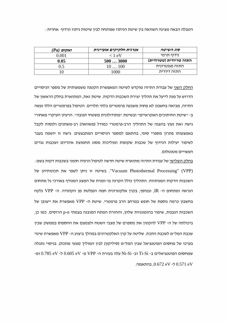
:אחרותניתוז ונידוף לבין שיטות שיטת הניתוז שפותחה השוואה בין ציגה הטבלה הבאה מ
סוג השיטה ית חלקיקים אופייניתאנרג (Pa)ואקום 0.001 < 1 eV נידוף תרמי )טטרודית(התזה טריודית 3000 … 500 0.05 התזה מגנטרונית 100 … 10 0.5 התזה דיודית 1000 10
מספר הניסויים של מאפשרת הקטנה משמעותית הזה מוקדש לשיטה יהתעבודת של החלק השני
ראשון של המתוארת בחלק ה ,שיטת זאת. ות הדקותת השכבתהליך יציראת לייעל על מנת הדרוש
הטיפול בפרמטרים הללו נעשה . פרמטרים בלתי תלוייםהלא פחות משבעמביאה בחשבון ,זהיהת
הרעיון העיקרי מאחורי ". חי תגובהט משתמתודולוגי"בשיטת ו" יםיאקראהחיתוכים השיטת "-ב
נסות לקבל משתנים ול-רב) משוואה(דל פרמטרי כמו-רבהתהליך ההצגה של נעוץ בגישה זאת
יושמה בעבר זוגישה . בצעיםמתהניסויים הבהתאם למספר , סופיפתרון מספרי באמצעותו
נגדים תחמוצת אינדיום ושכבות סוג ופות ומוליכות מקשכבות שלשיפור יעילות הנידוף של
. העשויים מטנטלום
:שכבות דקות בשםהרפיה חומני בול פ שיטה חדשה לטיתארוזה מתיהתעבודת של חלק השלישיב
"Vacuum Photothermal Processing" (VPP) . יהן שלונותכתאת לשפר בשיטה זו ניתן
של המצע המנודף באורכי גל מתחום תזמני- בוהתהליך כולל הקרנה. השכבות הדקות המנותזות
נלקח VPP -ה. חמה הנפלטת מן הקתודה תבקרן אלקטרוני, ובנוסף, IR -הנראה ומתחום ה
של ןייצובאת מאפשרת VPP -שיטת ה. פרמטרי רבהבחשבון כרמה נוספת של חופש במרחב
, כמו כן. הרוסיםp-nבצמתי החזרת המתח המובנה ו, ןהומוגניות שלהבשיפור , השכבות הנבנות
חספוס בממשק שבין צמצם את הלשטח והמצבי של םמספראת קטין להVPP -ביכולתה של ה
שינוי מאפשרת VPP-הביצוע במהלך םאלקטרוניהשליטה על קרן . תכתה תשכבלמ ''מלשכבת ה
בניסוי נתגלה ). מגעי מתכת(לבין המוליך ) סיליקון(מ "בין המלשפוטנציאל המחסום כו של ערב
- ומeV 0.785 - לeV 0.605 - מVPP -הבעזרת עלה Ni-Si - ובTi-Si - בםמחסום הפוטנציאליש
0.571 eV0.672 - ל eV,מה בהתא.


