
International Journal of Science and Research (IJSR) ISSN (Online): 2319-7064
Index Copernicus Value (2013): 6.14 | Impact Factor (2013): 4.438
Volume 4 Issue 5, May 2015
www.ijsr.net Licensed Under Creative Commons Attribution CC BY
Domino CMOS Implementation of Power
Optimized and High Performance CLA adder
Kistipati Karthik Reddy1, Jeeru Dinesh Reddy
2
1PG Student, BMS College of Engineering, Bull temple Road, Bengaluru, India
2Assistant Professor, BMS College of Engineering, Bull temple Road, Bengaluru, India
Abstract: A carry look-ahead adder enhances speed of addition since it produces final carry out before generating final sum.
Proposed work implements circuit design for a low-power high speed carry look ahead adder using Domino logic and results of
propagation delay, average and maximum power is calculated in high precise analog design environment(ADE).The technology node
assumed here is 180nm.Domino CMOS circuits enjoy area, delay and testability advantages over static circuits as such proposed
architecture is general and can be upgraded to NP Domino or Zipper circuits. The basic building blocks starting at transistor level and
logical blocks for adder and carry look-ahead logic is designed in Cadence Virtuoso cell-library and simulated in ADE_L.
Keywords: CMOS, ADE, CLA , LVS, DRC
1. Introduction
Advances in CMOS technology have led to a revived interest
in the design of basic functional blocks for digital systems.
As technology scaling no longer achieves constant power
density, the energy-efficiency of functional units is of
increasing importance to system designers. In electronics, an
adder or summer is a digital circuit that performs addition of
numbers. In many computers and other kinds of processors,
adders are used not only in the arithmetic logic unit, but also
in other parts of the processor, where they are used to
calculate addresses, table indices, and similar operations.
High-speed adders based on the CLA principle remain
dominant, since the carry delay can be improved by
calculating each stage in parallel. The Manchester carry
chain (MCC) is the most common dynamic (domino) CLA
adder architecture with a regular fast and simple structure[1]
adequate for implementation in VLSI.
Due to the fast changes happening in the semiconductor
technology the ability to pack more circuits in a small area
has increased many fold .And thus comes problem with our
conventional CMOS circuits, because it requires N+N=2N
no. of devices to perform a logic which can be a hardware
limitation in high density chips like SOCs. Dynamic CMOS
takes only N+2 logic gates compared to static CMOS
structures as mentioned above, taking upper edge over
CMOS. Other things which are not advantageous is PMOS
transistors are either heavy and slower[2] compared to
NMOS which may affect series connections to get slower.
2. Architecture
2.1 Domino logic
Dynamic gates are faster than static gates despite the extra
“evaluate” FET in the pull down path because of the
reduction in self-loading and the elimination of the pull up
short-circuit current during the first part of the output change.
An N-bit adder can be designed by modeling each blocks of a
CLA adder as shown in the figure.
Figure 1: showing Dynamic logic implementation
The main idea however is restricted to 4-bit adder as such the
complexity of adder increases with increase of bits thereon
requiring more no. of gates thus hardware.
2.2 Carry Look Ahead Adder
To reduce the computation time, engineers devised faster
ways to add two binary numbers by using carry-look ahead
adders. They work by creating two signals (P and G) for each
bit position, based on whether a carry is propagated through
from a less significant bit position (at least one input is a '1'),
generated in that bit position (both inputs are '1'), or killed in
that bit position (both inputs are '0'). In most cases, P is
simply the sum output of a half-adder and G is the carry
output of the same adder. After P and G are generated the
carries for every bit position are created. Some advanced
carry-look ahead architectures are the Manchester carry
chain, Brent–Kung adder, and the Kogge–Stone adder.
Paper ID: SUB154455 1301

International Journal of Science and Research (IJSR) ISSN (Online): 2319-7064
Index Copernicus Value (2013): 6.14 | Impact Factor (2013): 4.438
Volume 4 Issue 5, May 2015
www.ijsr.net Licensed Under Creative Commons Attribution CC BY
Figure 2: showing Domino CMOS logic implementation
Figure 3: showing a carry look ahead adder
3. Proposed System
3.1 Operational idea and system functionality
The operation of the single-stage dynamic CMOS logic gate
is quite straightforward. For practical multi-stage
applications, however, the dynamic CMOS gate presents a
significant problem. Domino logic is a CMOS-based
evolution of the dynamic logic techniques based on either
PMOS or NMOS transistors. It allows a rail-to-rail logic
swing and was developed to speed up circuits[3].
Domino CMOS logic gates allow a significant reduction in
the number of transistors required to realize any complex
Boolean function. The distribution of the clock signal within
the system is quite straightforward, since a single clock can
be used to precharge and evaluate any number of cascaded
stages, as long as the signal propagation delay from the first
stage to the last stage does not exceed the time span of the
evaluation phase. The limitation is that the number of
inverting static logic stages in cascade must be even, so that
the inputs of the next domino CMOS stage experience only 0
to 1 transitions during the evaluation. The precharging of all
high-capacitance nodes within the circuit effectively
eliminates all potential charge-sharing problems during
evaluation. The use of multiple precharge transistors also
enables us to use the precharged intermediate nodes as
resources for additional outputs. An additional logic
functions can be realized by tapping the internal nodes of the
dynamic CMOS stage.
The four functions of carry generation is to be realized are
listed in the following.
C1 = G1 + P1C0
C2 = G2 + P2G1 + P2P1C0
C3 =G3 + P3G2 + P3P2G1+ P3P2P1C0
C4 =G4 + P4G3 + P4P3G2 + P4P3P2G1 + P4P3P2P1C0
The functions Cl through C4 are the four carry terms to be
used in a four-stage carry-look ahead adder, where the
variables G0 and Pi are defined as
GI = AI * BI
PI =AI+BI
Where Ai and Bi are the input bits associated with the ith
stage. Hence, the circuit is also known as the Manchester
carry chain. The generation of the four carry terms using four
separate standard CMOS logic gates or four separate single-
output domino CMOS circuits, on the other hand, would
require a large number of transistors and consequently a
much larger silicon area. The transient performance of
domino CMOS logic gates can be improved by adjusting the
nMOS transistor sizes in the pull-down path, with the
objective of reducing the discharge time. The best
performance is obtained with a graded sizing of nMOS
transistors in series structures, where the nMOS transistor
closest to the output node also has the smallest (W/L) ratio.
3.2 Domino logic for carry generation
Domino implementation for carry generation in Cadence
virtuoso with a common clock structure is then fed through a
drive circuit having a carry look adder block. Each of the
PMOS and NMOS are connected to a common substrate and
no third-order effects are assumed while developing the
circuit for simulation. As each of logic block from carry is
complemented by CMOS and then fed to an inverter to get
the proper output.
Figure 4: showing carry logic block in multi-out Domino
logic
Paper ID: SUB154455 1302

International Journal of Science and Research (IJSR) ISSN (Online): 2319-7064
Index Copernicus Value (2013): 6.14 | Impact Factor (2013): 4.438
Volume 4 Issue 5, May 2015
www.ijsr.net Licensed Under Creative Commons Attribution CC BY
Figure 5: showing generate and propagate logic blocks
3.3 Proposed system
The proposed circuit diagram after all functional blocks are
added and carry logic along with generate pattern with
domino CMOS logic is shown below. The technology node
assumed to be λ=180nm. The clock used here is a general
(universal) clock for entire circuit, inputs to this block is Cin
from previous stage , propagate and generate functions which
are produced form sum blocks.
Figure 6: showing proposed system diagram logic
Sl.No. Component Quantity
1 AND gate 14
2 OR gate 8
3 XOR gate 8
As its sure that a total of 92 transistors are used to develop
logic using Domino whereas if used on by pseudo or pass
transistor logic the minimum number of transistors required
are 126.The adder circuit is implemented in Cadence
Virtuoso with analog design environment(ADE). Netlists are
generated and comparison of schematic with layout for DRC
and LVS checks are performed. It was found that both the
checks are satisfactory and are in good agreement with
technology node. Final stage is to extract parasitic
capacitances and resistors to be compared with wire load
modules(WLM) is suggested.
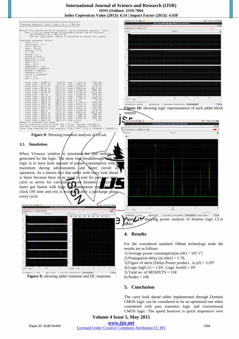
3.4 Synthesis report
The transient and steady state analysis of a carry look ahead
adder with domino logic implementation at a time frame of
300ns is observed for throughput and its results are observed.
Figure 7: showing steady state(DC) analysis
Paper ID: SUB154455 1303
International Journal of Science and Research (IJSR) ISSN (Online): 2319-7064
Index Copernicus Value (2013): 6.14 | Impact Factor (2013): 4.438
Volume 4 Issue 5, May 2015
www.ijsr.net Licensed Under Creative Commons Attribution CC BY
Figure 8: Showing transient analysis of circuit
3.5 Simulation
When Virtuoso window is simulated for and netlists are
generated for the logic. The most vital breakthrough with the
logic is to have least amount of power consumption with a
maximum during sub-transients and faster circuit of
operation. As a known fact that adder with carry look ahead
is faster because there in no need to wait for previous stage
carry to arrive for calculation, with dynamic circuits the
faster got fastest with logic implementation reserved for a
clock ON time and rest is evaluated after a precharge phase
every cycle.
Figure 9: showing adder transient and DC response
Figure 10: showing logic representation of each adder block
outputs
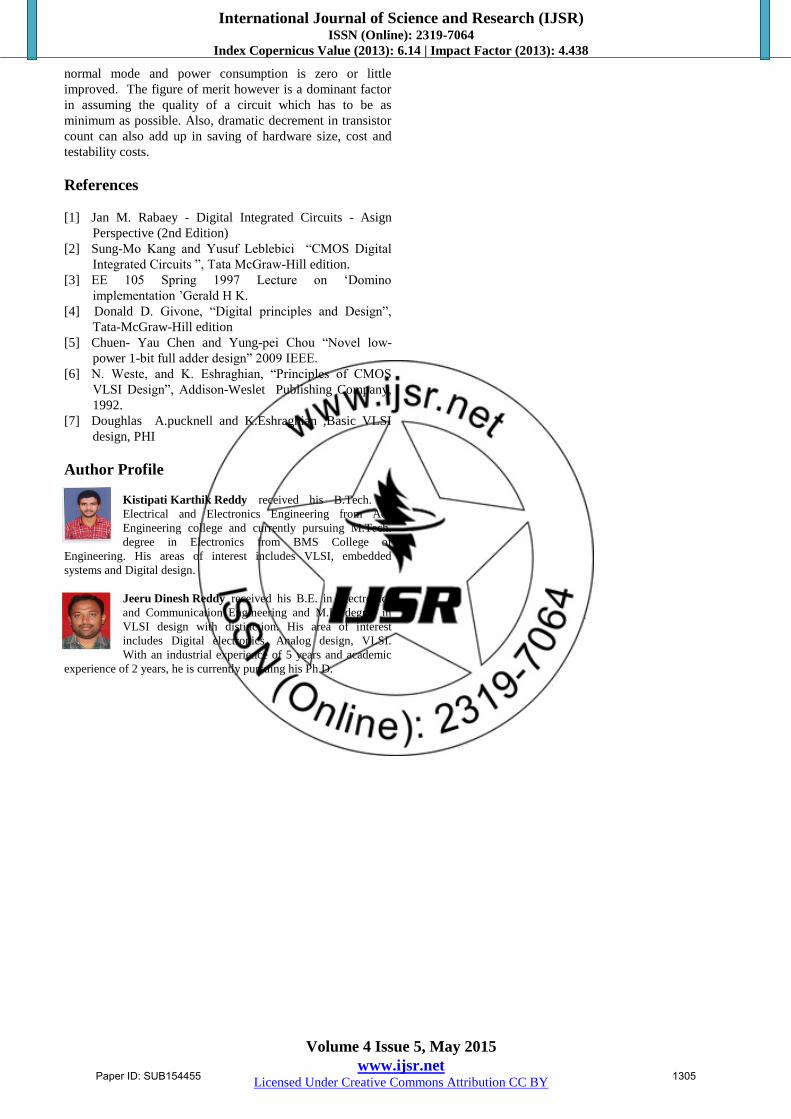
Figure 11: showing power analysis of domino logic CLA
adder
4. Results
For the considered standard 180nm technology node the
results are as follows
1) Average power consumption(in uW) = 187.17,
2) Propagation delay (in nSec) = 1.76,
3) Figure of merit (Delay-Power product , in pJ) = 3.297
4) Logic high (1) = 1.8V, Logic low(0) = 0V
5) Total no. of MOSFETS = 158
6) Nodes = 106
5. Conclusion
The carry look ahead adder implemented through Domino
CMOS logic can be considered to be an optimized one when
considered with pass transistor logic and conventional
CMOS logic. The speed however is quick responsive over
Paper ID: SUB154455 1304
International Journal of Science and Research (IJSR) ISSN (Online): 2319-7064
Index Copernicus Value (2013): 6.14 | Impact Factor (2013): 4.438
Volume 4 Issue 5, May 2015
www.ijsr.net Licensed Under Creative Commons Attribution CC BY
normal mode and power consumption is zero or little
improved. The figure of merit however is a dominant factor
in assuming the quality of a circuit which has to be as
minimum as possible. Also, dramatic decrement in transistor
count can also add up in saving of hardware size, cost and
testability costs.
References
[1] Jan M. Rabaey - Digital Integrated Circuits - Asign
Perspective (2nd Edition)
[2] Sung-Mo Kang and Yusuf Leblebici “CMOS Digital
Integrated Circuits ”, Tata McGraw-Hill edition.
[3] EE 105 Spring 1997 Lecture on „Domino
implementation ‟Gerald H K.
[4] Donald D. Givone, “Digital principles and Design”,
Tata-McGraw-Hill edition
[5] Chuen- Yau Chen and Yung-pei Chou “Novel low-
power 1-bit full adder design” 2009 IEEE.
[6] N. Weste, and K. Eshraghian, “Principles of CMOS
VLSI Design”, Addison-Weslet Publishing Company,
1992.
[7] Doughlas A.pucknell and K.Eshraghian ,Basic VLSI
design, PHI
Author Profile
Kistipati Karthik Reddy received his B.Tech. in
Electrical and Electronics Engineering from Ace
Engineering college and currently pursuing M.Tech.
degree in Electronics from BMS College of
Engineering. His areas of interest includes VLSI, embedded
systems and Digital design.
Jeeru Dinesh Reddy received his B.E. in Electronics
and Communication Engineering and M.E. degree in
VLSI design with distinction. His area of interest
includes Digital electronics, Analog design, VLSI.
With an industrial experience of 5 years and academic
experience of 2 years, he is currently pursuing his Ph.D.
Paper ID: SUB154455 1305


