
ECE 260B – CSE 241A Cost/Mfg 1 Andrew B. Kahng, UCSD
ECE260B – CSE241AWinter 2007
Cost and Manufacturing – Part 1
Website: http://vlsicad.ucsd.edu/courses/ece260b-w07
ECE 260B – CSE 241A Cost/Mfg 2 Andrew B. Kahng, UCSD
Overview of Cost
Source: Nassda Corporation
ECE 260B – CSE 241A Cost/Mfg 3 Andrew B. Kahng, UCSD
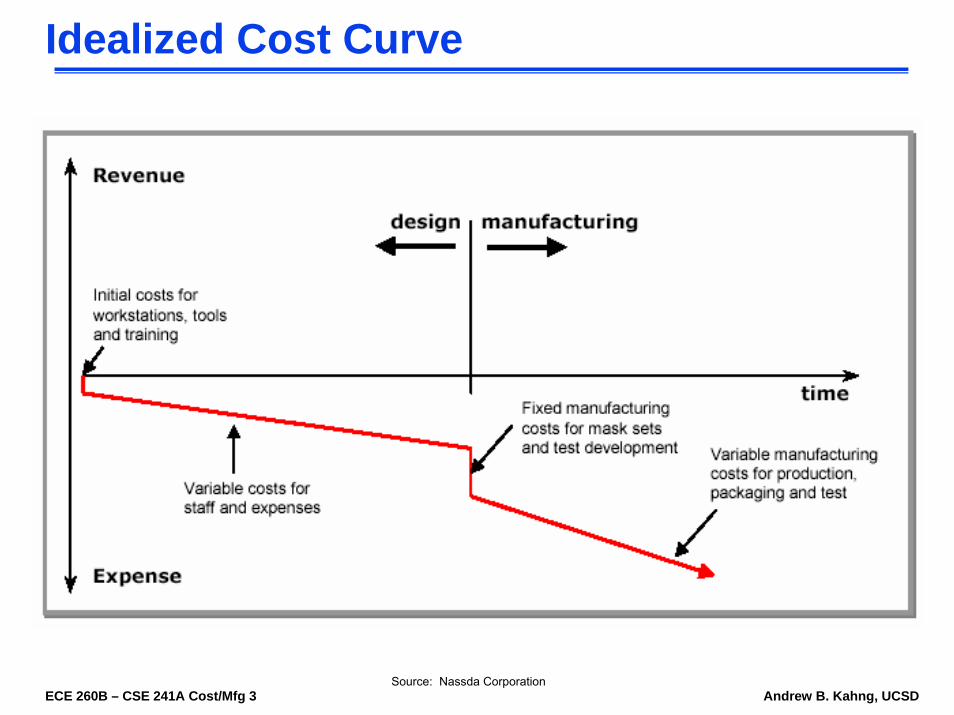
Idealized Cost Curve
Source: Nassda Corporation
ECE 260B – CSE 241A Cost/Mfg 4 Andrew B. Kahng, UCSD
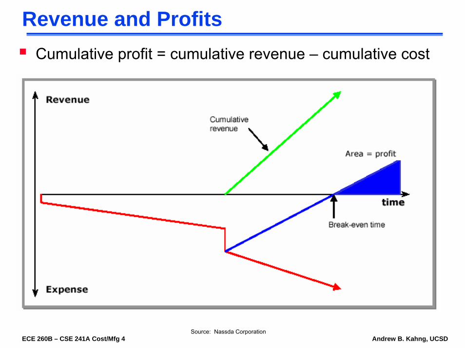
Revenue and ProfitsCumulative profit = cumulative revenue – cumulative cost
Source: Nassda Corporation

ECE 260B – CSE 241A Cost/Mfg 5 Andrew B. Kahng, UCSD
Impact of RespinsSeverely delays time-to-profit
first-time successful silicon, time-to-market are everything
Source: Nassda Corporation

ECE 260B – CSE 241A Cost/Mfg 6 Andrew B. Kahng, UCSD
Distribution of Respin Counts
10.34%
31.03% 31.03 %
10.34 %
17.24 %
1 2 3 4 5 Or More
Probability
Spin Count
Silicon Spins, High Complexity Communications ICs*
High AnalogContent
10%
20%
30%
First-timeSilicon Success *High Complexity = >1 Million Complexity Units
Source: Ron Collett, Numetrics (DAC-2002 panel)
ECE 260B – CSE 241A Cost/Mfg 7 Andrew B. Kahng, UCSD
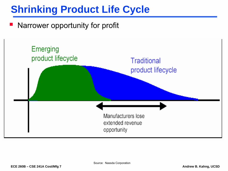
Shrinking Product Life CycleNarrower opportunity for profit
Source: Nassda Corporation
ECE 260B – CSE 241A Cost/Mfg 8 Andrew B. Kahng, UCSD
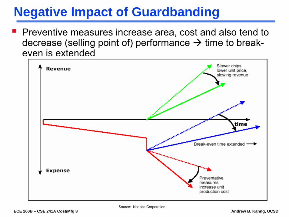
Negative Impact of GuardbandingPreventive measures increase area, cost and also tend to decrease (selling point of) performance time to break-even is extended
Source: Nassda Corporation
ECE 260B – CSE 241A Cost/Mfg 9 Andrew B. Kahng, UCSD
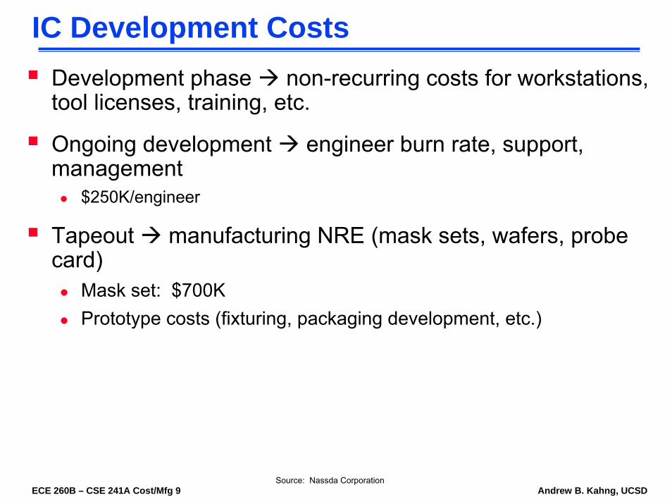
IC Development CostsDevelopment phase non-recurring costs for workstations, tool licenses, training, etc.
Ongoing development engineer burn rate, support, management
$250K/engineer
Tapeout manufacturing NRE (mask sets, wafers, probe card)
Mask set: $700KPrototype costs (fixturing, packaging development, etc.)
Source: Nassda Corporation

ECE 260B – CSE 241A Cost/Mfg 10 Andrew B. Kahng, UCSD
System Costs
Source: Nassda Corporation

ECE 260B – CSE 241A Cost/Mfg 11 Andrew B. Kahng, UCSD
Silicon (Die) Costs200mm wafer with 25 mask levels: $2750
2mm edge unusable area = 30,171 mm2
Cost per mm2 = 9.11 cents
300mm wafer at mature 90nm will cost ~$3500 - $50005 cents per mm2
Helps keep Moore’s Law on track
ITRS: Reduce the 2mm edge to 1mm 1.3% more wafer area (about 10 days of Moore’s Law …)
Source: Nassda Corporation

ECE 260B – CSE 241A Cost/Mfg 12 Andrew B. Kahng, UCSD
YieldA manufacturing defect is a finite chip area with electrically malfunctioning circuitry caused by errors in the fabrication process
A chip with no manufacturing defect is called a (functionally) good chip
Fraction (or percentage) of good chips produced in a manufacturing process is called the yield
Yield is denoted by symbol Y
Cost of a chip:Cost of fabricating and testing a wafer
--------------------------------------------------Yield x Number of chip sites on the wafer
Source: Hessabi, Sharif Univ.

ECE 260B – CSE 241A Cost/Mfg 13 Andrew B. Kahng, UCSD
Why Yield / Area Are ImportantConsider a cellphone chip
Sells (say) 10M copiesDesign house pays (say) $5K/300mm 90nm wafer and $6K for 65nm wafer10mmX10mm chip size at 90nm ~700 die/wafer (assume 100% yield)Scaled to 65nm 7mmX7mm ~1400 die/wafer
- Need min. 60% yield at 65nm for same cost as 90nm (not accounting for design time, etc)
- If I get 100% yield at 65nm, I save ~$30M!! Not counting TTM value
What matters is good die/wafer however you get itBetter P&R tools, better foundry equipment …Better designers, better lithographers, better device engineers,…
Justifies the existence of even the “half-nodes”110nm, 80nm, 55nm….
Source: Hessabi, Sharif Univ.
ECE 260B – CSE 241A Cost/Mfg 14 Andrew B. Kahng, UCSD
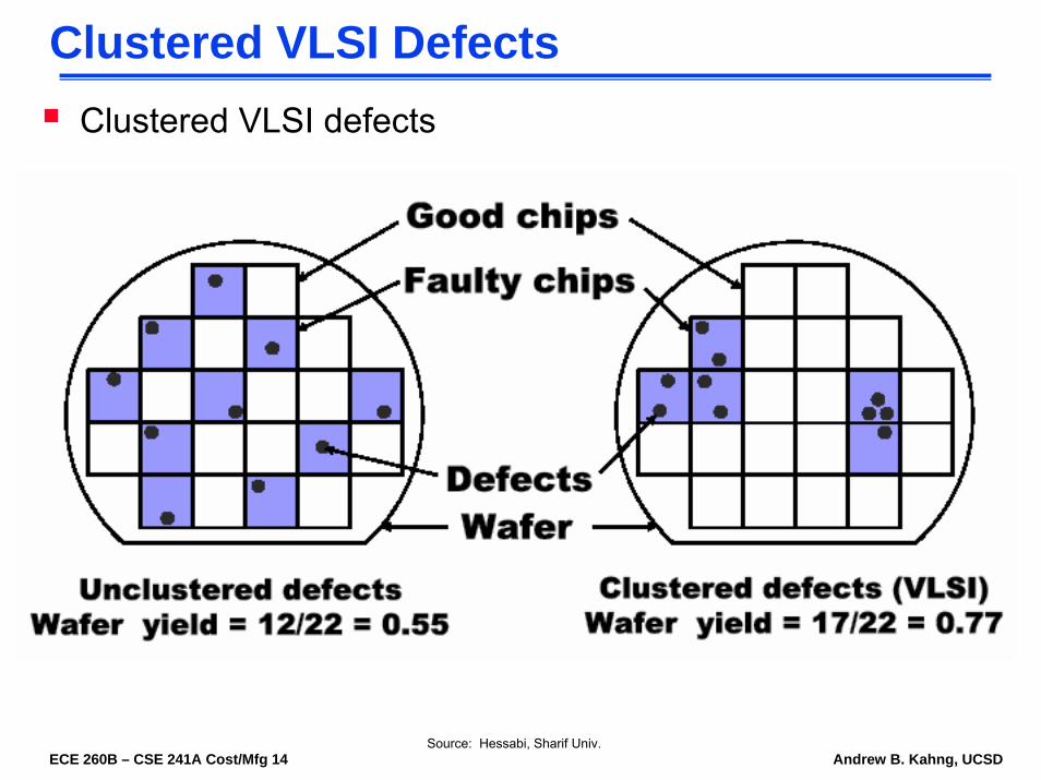
Clustered VLSI DefectsClustered VLSI defects
Source: Hessabi, Sharif Univ.

ECE 260B – CSE 241A Cost/Mfg 15 Andrew B. Kahng, UCSD
Yield Parameters and Yield EquationDefect density d = average #defects per unit chip areaChip area (A), defect clustering parameter (α)Negative binomial distribution of defects
p(x) = Prob (#defects on chip = x)
Γ(α+x) (Ad /α) x
= ----------- X ----------------x ! Γ(α) (1+Ad /α) α+x
where Γ is the gamma functionα =0 p(x) is a delta function (maximum clustering)α = ∞ p(x) is Poisson distribution (no clustering)
Yield Y = Prob (#defects = 0) = ( 1 + Ad / α ) -αExample: Ad = 1.0, α = 0.5, Y = 0.58Unclustered defects: α = ∞ , Y = e-Ad
- Example: Ad = 1.0, α = ∞ , Y = 0.37 unclustered is pessimisticSource: Hessabi, Sharif Univ.
ECE 260B – CSE 241A Cost/Mfg 16 Andrew B. Kahng, UCSD
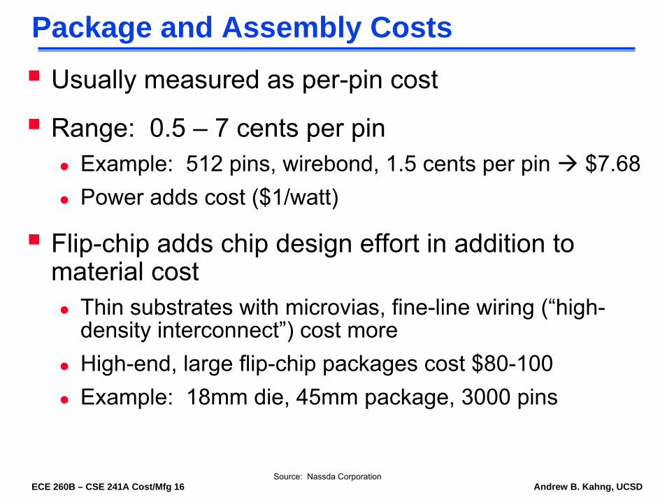
Package and Assembly CostsUsually measured as per-pin cost
Range: 0.5 – 7 cents per pinExample: 512 pins, wirebond, 1.5 cents per pin $7.68Power adds cost ($1/watt)
Flip-chip adds chip design effort in addition to material cost
Thin substrates with microvias, fine-line wiring (“high-density interconnect”) cost moreHigh-end, large flip-chip packages cost $80-100Example: 18mm die, 45mm package, 3000 pins
Source: Nassda Corporation

ECE 260B – CSE 241A Cost/Mfg 17 Andrew B. Kahng, UCSD
Design for TestDesign for Test on chip impacts board, system level economics
Costs- Reduced yield due to area- Overhead, yield loss due to non-functional tests
Benefits- Reduced ATE cost due to self-test- Less expensive alternatives to burn-in
Source: Hessabi, Sharif Univ.

ECE 260B – CSE 241A Cost/Mfg 18 Andrew B. Kahng, UCSD
Test CostsTest cost depends on time spent on ATEExample: 15 seconds @ $250/hr = $3.75
Ranges: 5-60 seconds, $50-500/hour
Example: Year 2000 mid-range mfg test costATE: 0.5-1.0GHz, analog instruments,1,024 digital pins: purchase price = $1.2M + 1,024 x $3,000 = $4.272MRunning cost (5-yr linear depreciation) = Depreciation + Maintenance + Operation = $0.854M + $0.085M + $0.5M = $1.439M/yearTest cost (24 hour ATE operation) = $1.439M/(365 x 24 x 3,600) = 4.5 cents/second
- (previous example: 6.94 cents/sec)
Key phrases: Test compression, pincount reductionSource: Hessabi, Sharif Univ.
ECE 260B – CSE 241A Cost/Mfg 19 Andrew B. Kahng, UCSD
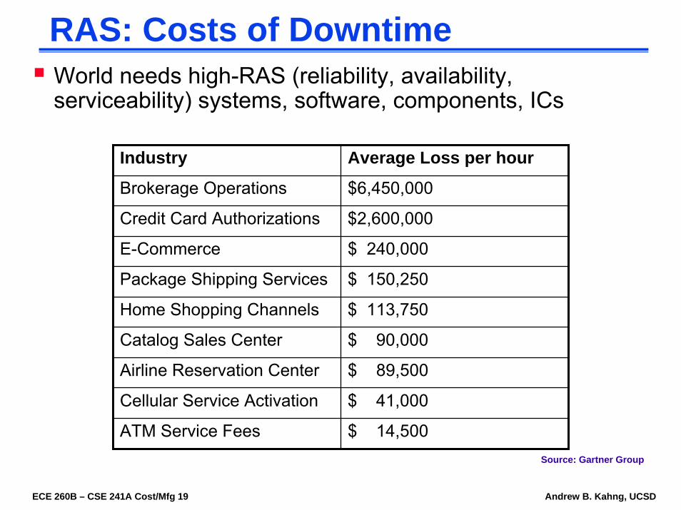
RAS: Costs of DowntimeWorld needs high-RAS (reliability, availability, serviceability) systems, software, components, ICs
Industry Average Loss per hour
Brokerage Operations $6,450,000
Credit Card Authorizations $2,600,000
E-Commerce $ 240,000
Package Shipping Services $ 150,250
Home Shopping Channels $ 113,750
Catalog Sales Center $ 90,000
Airline Reservation Center $ 89,500
Cellular Service Activation $ 41,000
ATM Service Fees $ 14,500Source: Gartner Group

ECE 260B – CSE 241A Cost/Mfg 20 Andrew B. Kahng, UCSD
Estimation of RAS ParametersHigh level RAS Metrics
mean time before failure (MTBF), mean time to failure (MTTF), mean time to repair (MTTR)total uptime or down time of the system in a yearfive 9’s reliability (99.999%), three 9’s reliability (99.9%)need to estimate for active and passive components, boards and systems
Low level RAS Metricsbit error rates, bit flips per second, packets lost per second, packets dropped per secondfailures or glitches in components per secondunintentional failures per second, and intentional failures per second
Estimation tools tightly couple RAS metrics with functionality, performance and cost of the systemearly in the design cycle accuracy is not high (50%)at final system development accuracy must improve to 10%

ECE 260B – CSE 241A Cost/Mfg 21 Andrew B. Kahng, UCSD
Design Costs
Source: Nassda Corporation
ECE 260B – CSE 241A Cost/Mfg 22 Andrew B. Kahng, UCSD
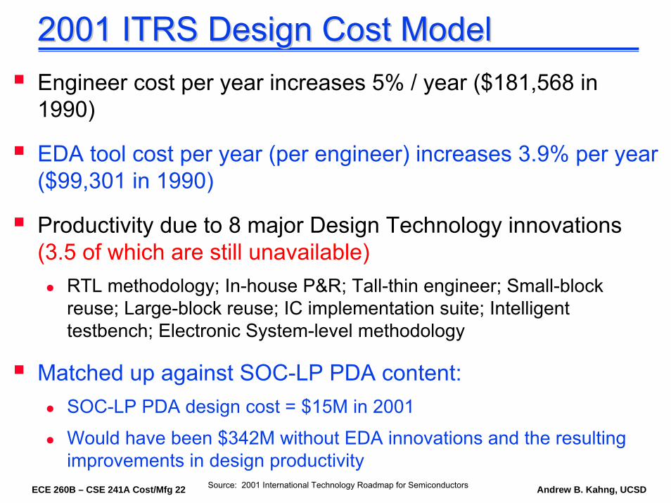
2001 ITRS Design Cost Model2001 ITRS Design Cost ModelEngineer cost per year increases 5% / year ($181,568 in 1990)
EDA tool cost per year (per engineer) increases 3.9% per year ($99,301 in 1990)
Productivity due to 8 major Design Technology innovations (3.5 of which are still unavailable)
RTL methodology; In-house P&R; Tall-thin engineer; Small-block reuse; Large-block reuse; IC implementation suite; Intelligent testbench; Electronic System-level methodology
Matched up against SOC-LP PDA content:SOC-LP PDA design cost = $15M in 2001
Would have been $342M without EDA innovations and the resulting improvements in design productivity
Source: 2001 International Technology Roadmap for Semiconductors
ECE 260B – CSE 241A Cost/Mfg 23 Andrew B. Kahng, UCSD
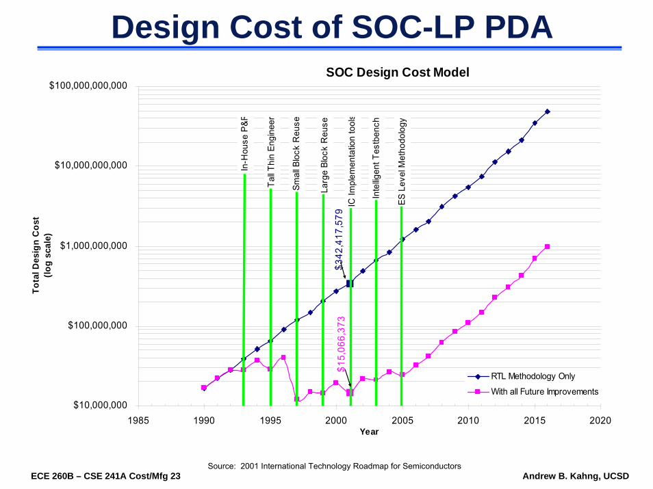
SOC Design Cost Model
$342
,417
,579
$15,
066,
373
$10,000,000
$100,000,000
$1,000,000,000
$10,000,000,000
$100,000,000,000
1985 1990 1995 2000 2005 2010 2015 2020Year
Tota
l Des
ign
Cos
t (lo
g sc
ale)
RTL Methodology Only
With all Future Improvements
In-H
ouse
P&R
Tall T
hin
Engi
neer
Smal
l Blo
ck R
euse
IC Im
plem
enta
tion
tool
s
Larg
e Bl
ock
Reu
se
Inte
lligen
t Tes
tben
ch
ES L
evel
Met
hodo
logy
Design Cost of SOC-LP PDA
Source: 2001 International Technology Roadmap for Semiconductors

ECE 260B – CSE 241A Cost/Mfg 24 Andrew B. Kahng, UCSD
Factors Affecting Success
Chip Complexity = ƒ(circuit types, timing, reuse, power . . .)
Design Productivity =Effort = ƒ(Eng. & mgmt. skills, EDA tools, spec stability,
mfg. process stability, etc.)
Complexity
Effort
Rate of Effort Consumption = ƒ(best practices)
Quality of Design Process, e.g. spin count probability density function
Key milestones, e.g. ƒ(effort consumed, bug rate)
Source: Ron Collett, Numetrics (DAC-2002 panel)

ECE 260B – CSE 241A Cost/Mfg 25 Andrew B. Kahng, UCSD
Modeling of Design Complexity vs. Effort
Complexity Units (Millions)R2 Defined
Actual Project Effort(Person-weeks)
Perfect Fit: R2 = 1No Correlation: R2 = 0
Relationship Between Predicted Project Effort and Actual Project Effort
R2 = 0.52 (CU < 900K)R2 = 0.62 (CU > 900K)
0
2,000
4,000
6,000
8,000
10,000
0 0.2 0.4 0.6 0.8 1 1.2 1.4 1.6 1.8
Source: Ron Collett, Numetrics (DAC-2002 panel)

ECE 260B – CSE 241A Cost/Mfg 26 Andrew B. Kahng, UCSD
Modeling of Design Productivity
Design Productivity vs. Peak Staffing
Des
ign
Prod
ucti
vity
Peak Staffing
= IC Projects
Source: Ron Collett, Numetrics (DAC-2002 panel)
ECE 260B – CSE 241A Cost/Mfg 27 Andrew B. Kahng, UCSD
Cost Savings – Silicon, NRE
Source: Nassda Corporation

ECE 260B – CSE 241A Cost/Mfg 28 Andrew B. Kahng, UCSD
How to Save Total NRE + Wafer Cost?Multi-project wafers
Not just packing dependentDepends on similar densities, speeds, etc. (process biases)Depends on volumes
Metal-only respinsSpare (“bonus”) resources in synthesis, layout
How to allocate? How to locate?
Source: Hessabi, Sharif Univ.
ECE 260B – CSE 241A Cost/Mfg 29 Andrew B. Kahng, UCSD
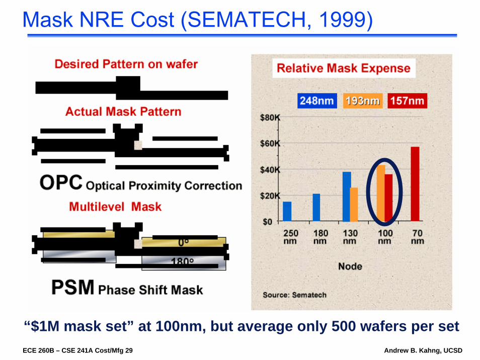
Mask NRE Cost (SEMATECH, 1999)
“$1M mask set” at 100nm, but average only 500 wafers per set
ECE 260B – CSE 241A Cost/Mfg 30 Andrew B. Kahng, UCSD
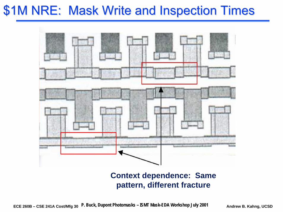
Context dependence: Same pattern, different fracture
P. Buck, Dupont Photomasks – ISMT Mask-EDA Workshop July 2001
$1M NRE: Mask Write and Inspection Times$1M NRE: Mask Write and Inspection Times

ECE 260B – CSE 241A Cost/Mfg 31 Andrew B. Kahng, UCSD
$1M NRE: Mask Write and Inspection Times$1M NRE: Mask Write and Inspection TimesToo many data formats
Most tools have unique data formatRaster to variable shaped-beam conversion is inefficientReal-time manufacturing tool switch, multiple qualified toolsduplicate fractures to avoid delays if tool switch required
Data volumeOPC increases figure count accelerationMEBES format is flatALTA machines (laser mask writers) slow down with > 1GB dataData volume strains distributed manufacturing resources
Refracturing mask data90% of mask data files manipulated or refractured: process bias sizing (iso-dense, loading effects, linearity, …), mask write optimization, multiple tool formats, …
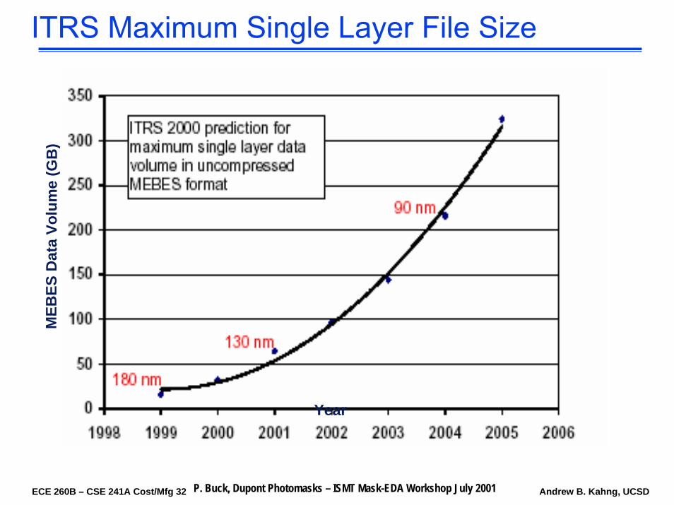
ECE 260B – CSE 241A Cost/Mfg 32 Andrew B. Kahng, UCSD
MEB
ES D
a ta
Volu
me
( GB
)
Year
P. Buck, Dupont Photomasks – ISMT Mask-EDA Workshop July 2001
ITRS Maximum Single Layer File Size

ECE 260B – CSE 241A Cost/Mfg 33 Andrew B. Kahng, UCSD
ABF Data Volume (MB)
Writ
e Ti
me
(Re f
orm
at +
Pr in
t ) ( H
r s)
P. Buck, Dupont Photomasks – ISMT Mask-EDA Workshop July 2001
Mask Write Time vs. Data Volume
ECE 260B – CSE 241A Cost/Mfg 34 Andrew B. Kahng, UCSD
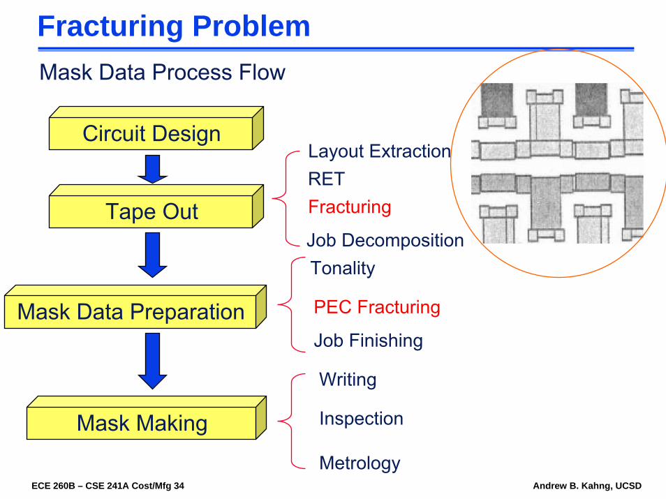
Fracturing ProblemMask Data Process Flow
Layout ExtractionRET
Circuit Design
Tape OutJob Decomposition
Mask Data Preparation
Mask Making
Writing
Inspection
Metrology
Tonality
PEC Fracturing
Job Finishing
Fracturing

ECE 260B – CSE 241A Cost/Mfg 35 Andrew B. Kahng, UCSD
Challenges in Fracturing
• A shot whose minimum width < ε is called a sliver
< ε
sliverslant
• # shots increase mask writing time increase cost increase
• each shot should be an axis-parallel trapezoid• the side size of each shot < M
• slant edges should not be partitioned
• # slivers increase mask error enhancement factor (MEEF) increaselarger CD variation and error yield decrease

ECE 260B – CSE 241A Cost/Mfg 36 Andrew B. Kahng, UCSD
Fracturing Problem
a list of polygons P with axis parallel and slant edges
Max shot size M
Slivering size ε
Partition P into non-overlapping trapezoidal shots
Number of shots and number of slivers
Given:
Minimizing:
Normal fracturing Reverse tone fracturing
ECE 260B – CSE 241A Cost/Mfg 37 Andrew B. Kahng, UCSD
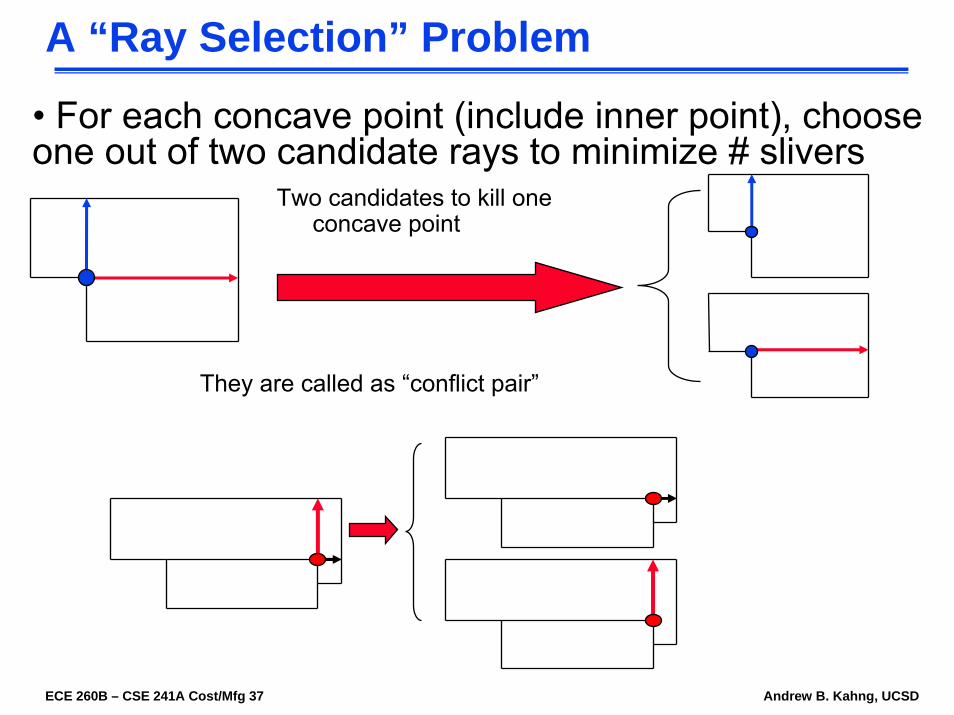
A “Ray Selection” Problem
Two candidates to kill one concave point
• For each concave point (include inner point), choose one out of two candidate rays to minimize # slivers
They are called as “conflict pair”
ECE 260B – CSE 241A Cost/Mfg 38 Andrew B. Kahng, UCSD
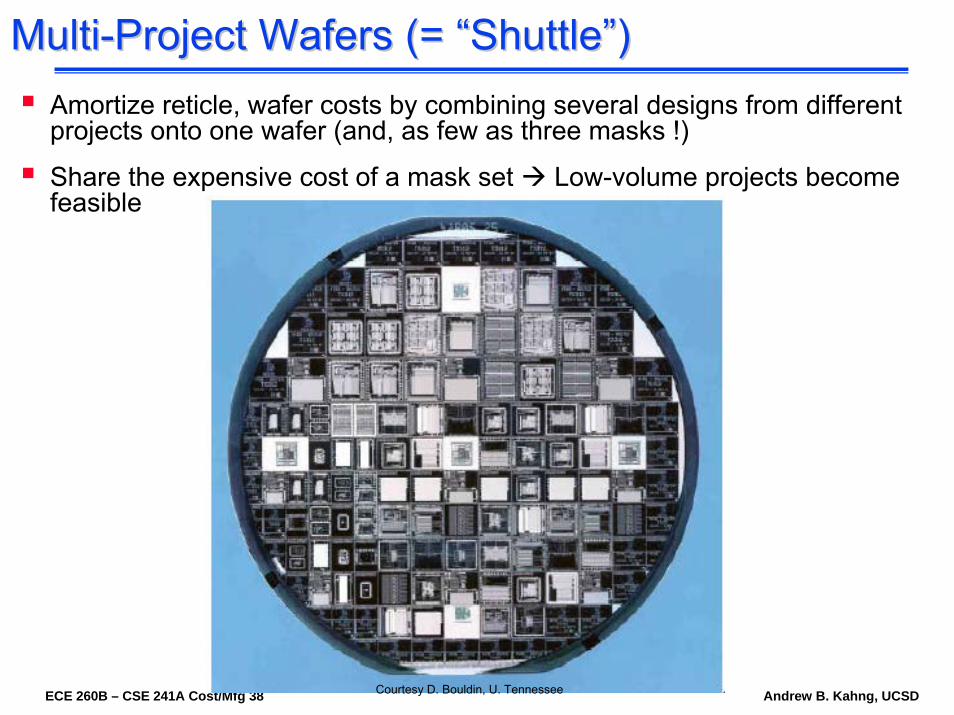
MultiMulti--Project Wafers (= Project Wafers (= ““ShuttleShuttle””))Amortize reticle, wafer costs by combining several designs from different projects onto one wafer (and, as few as three masks !)
Share the expensive cost of a mask set Low-volume projects become feasible
Courtesy D. Bouldin, U. Tennessee

ECE 260B – CSE 241A Cost/Mfg 39 Andrew B. Kahng, UCSD
MPW Design Flow
Four Steps of Design Flow
Die Assignment
Placement
Shotmap
Stepper
Dicing Plan
Reticle
ECE 260B – CSE 241A Cost/Mfg 40 Andrew B. Kahng, UCSD
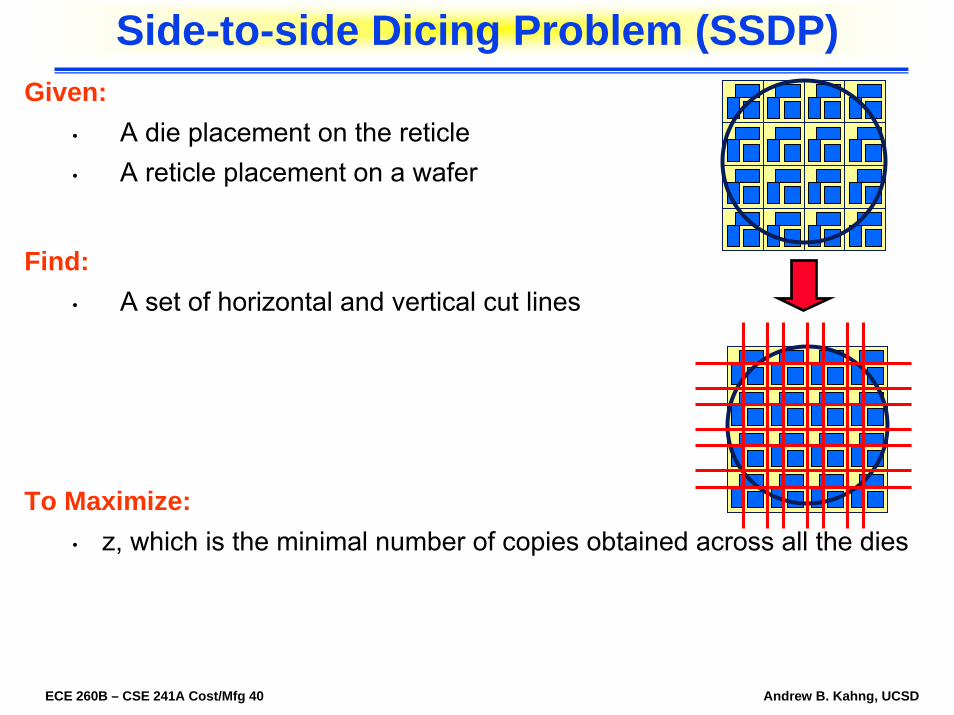
Side-to-side Dicing Problem (SSDP)Given:
• A die placement on the reticle• A reticle placement on a wafer
Find:• A set of horizontal and vertical cut lines
To Maximize:• z, which is the minimal number of copies obtained across all the dies
ECE 260B – CSE 241A Cost/Mfg 41 Andrew B. Kahng, UCSD
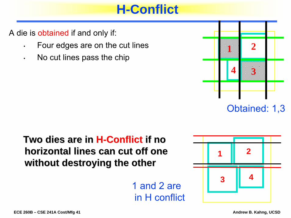
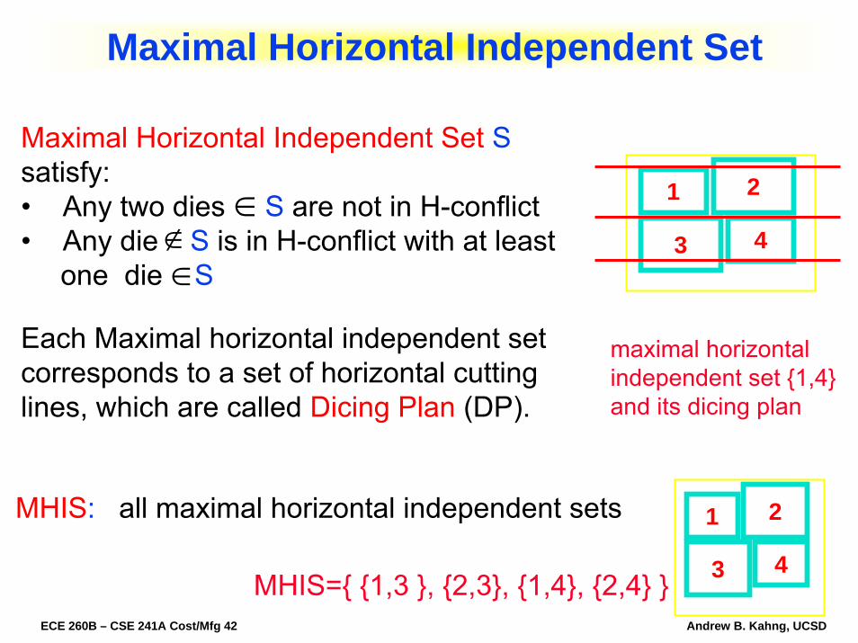
H-ConflictA die is obtained if and only if:
• Four edges are on the cut lines• No cut lines pass the chip
1 2
4 3
Obtained: 1,3
Two dies are in Two dies are in HH--ConflictConflict if no if no horizontal lines can cut off one horizontal lines can cut off one without destroying the other without destroying the other
1 2
431 and 2 are in H conflict
ECE 260B – CSE 241A Cost/Mfg 42 Andrew B. Kahng, UCSD
MHIS={ {1,3 }, {2,3}, {1,4}, {2,4} }
Maximal Horizontal Independent Set S satisfy: • Any two dies S are not in H-conflict• Any die S is in H-conflict with at least
one die S
Each Maximal horizontal independent set corresponds to a set of horizontal cutting lines, which are called Dicing Plan (DP).
MHIS: all maximal horizontal independent sets
1 2
43∈
∉∈
maximal horizontal independent set {1,4} and its dicing plan
1 2
43
Maximal Horizontal Independent Set
ECE 260B – CSE 241A Cost/Mfg 43 Andrew B. Kahng, UCSD
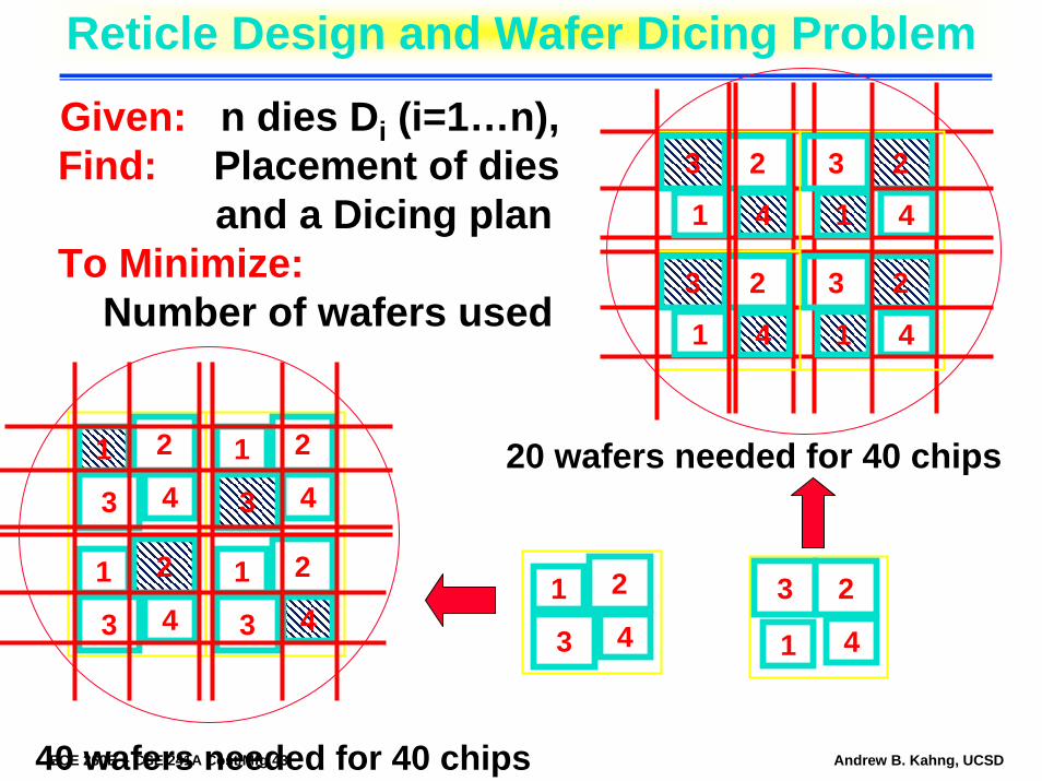
Reticle Design and Wafer Dicing Problem
Given: n dies Di (i=1…n), Find: Placement of dies
and a Dicing planTo Minimize:
Number of wafers used
1 2
43
1 2
43
1 2
43
1 2
43
2
4
2
4
1
2
4
3
1
3
1
2
4
3
1
3
40 wafers needed for 40 chips
20 wafers needed for 40 chips
1 2
43 1
2
4
3

ECE 260B – CSE 241A Cost/Mfg 44 Andrew B. Kahng, UCSD
Shot-Map and Stepping Problem
• Layout of reticle on multi-project wafer can have significant impact on die yield
• Objective: max weighted die yieldyield probability- defect distributions
- edge loss
weights (target production volumes, etc.) for different designs

ECE 260B – CSE 241A Cost/Mfg 45 Andrew B. Kahng, UCSD
Yield Modeling - Defect Density Models• Poisson
random or even defect distribution
• Murphysymmetrical triangular distribution [0, 2D] with peak at D
• Negative-Binomial (Seeds)defect clustering
α: cluster parameter
• Bose-Einsteinfatal defects: in certain critical mask layers
n : # critical mask layers

ECE 260B – CSE 241A Cost/Mfg 46 Andrew B. Kahng, UCSD
• Edge radial yield degradationWafer yields degrade with closer proximity of the wafer perimeterMore important with larger wafer dimension- 200mm 300mm (average 12mm X 12mm chip)
⇒ about 60% more chips that are bordering wafer perimeter
• Radial yield model [Teets 94]
r : distance of reticle from wafer center ∂ and β- empirically determined variables- functions of chip size
Wafer Radial Yield
( )( )1
1radial
rY
e β∂ −=
+
ECE 260B – CSE 241A Cost/Mfg 47 Andrew B. Kahng, UCSD
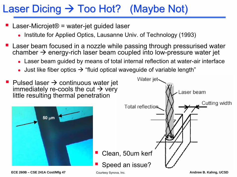
Laser Dicing Laser Dicing Too Hot? (Maybe Not)Too Hot? (Maybe Not)Laser-Microjet® = water-jet guided laser
Institute for Applied Optics, Lausanne Univ. of Technology (1993)
Laser beam focused in a nozzle while passing through pressurised water chamber energy-rich laser beam coupled into low-pressure water jet
Laser beam guided by means of total internal reflection at water-air interfaceJust like fiber optics “fluid optical waveguide of variable length”
Courtesy Synova, Inc.
Pulsed laser continuous water jet immediately re-cools the cut very little resulting thermal penetration
Clean, 50um kerf
Speed an issue?
ECE 260B – CSE 241A Cost/Mfg 48 Andrew B. Kahng, UCSD
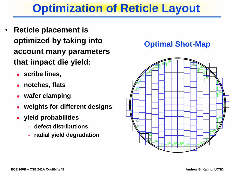
• Reticle placement is optimized by taking into account many parameters that impact die yield:
scribe lines, notches, flats wafer clampingweights for different designsyield probabilities
- defect distributions- radial yield degradation
Optimal Shot-Map
Optimization of Reticle Layout

ECE 260B – CSE 241A Cost/Mfg 49 Andrew B. Kahng, UCSD
Readingshttp://www.dac.com/38th/acceptedpapers.nsf/9cfb1ebaaf59043587256a6a00031f78/5383bbf67973bfc488256a78006d4b42/$FILE/2_2.PDF (W. Maly invited paper, Session 2, DAC-2001 – “IC Design in High-Cost Nanometer-Technologies Era”
http://www.nassda.com/ROIWhitePaper.pdf (Nassda Corporation, “Maximizing Silicon ROI: The Cost of Failure and Success”)
See also Wright, Williams and Kelly website (SEMATECH Cost of Ownership Model)
ECE 260B – CSE 241A Cost/Mfg 50 Andrew B. Kahng, UCSD
Homework 2/21, Due Wednesday 2/28Question 1. How does the semiconductor industry achieve low-volume IC production with, say, just three photomasks even though the chip has device, interconnect, and contact/via shapes? Explain and give a concrete example.
Question 2. Determine the number of die of size {7x7, 10x10, 14x14} mm^2 that can fit within a {200, 300} mm (diameter) wafer. If a die having any portion within 15mm of the wafer edge will fail, then how many good die will be obtained per wafer in the above 6 scenarios? (Find a utility on the web, or write your own code, to help answer this.)


