
EEC 118 Lecture #11:CMOS Design GuidelinesAlternative Static Logic
FamiliesRajeevan Amirtharajah
University of California, Davis
Jeff ParkhurstIntel Corporation

Amirtharajah/Parkhurst, EEC 118 Spring 2010 4
Outline
• Finish Arithmetic Discussion
• Review: Static CMOS Sizing
• Design Guidelines for CMOS
• Pseudo-NMOS Logic: Rabaey 6.2
• Pass Transistor Circuits: Rabaey 6.2 (Kang & Leblebici 9.1-9.2)

Amirtharajah/Parkhurst, EEC 118 Spring 2010 5
Review: CMOS Sizing• Equivalent inverter approach: replace transistors
which are “on” with equivalent transistor
• Use equivalent inverter to find VM, delays, etc.
if A=0, B switches:
A
B
A B
F
Wna Wnb
Wpb
Wpa Wpeff
Wneff
B F
nbneff
pbpapeff
WW
WWW
=
+=111
Amirtharajah/Parkhurst, EEC 118 Spring 2010 6
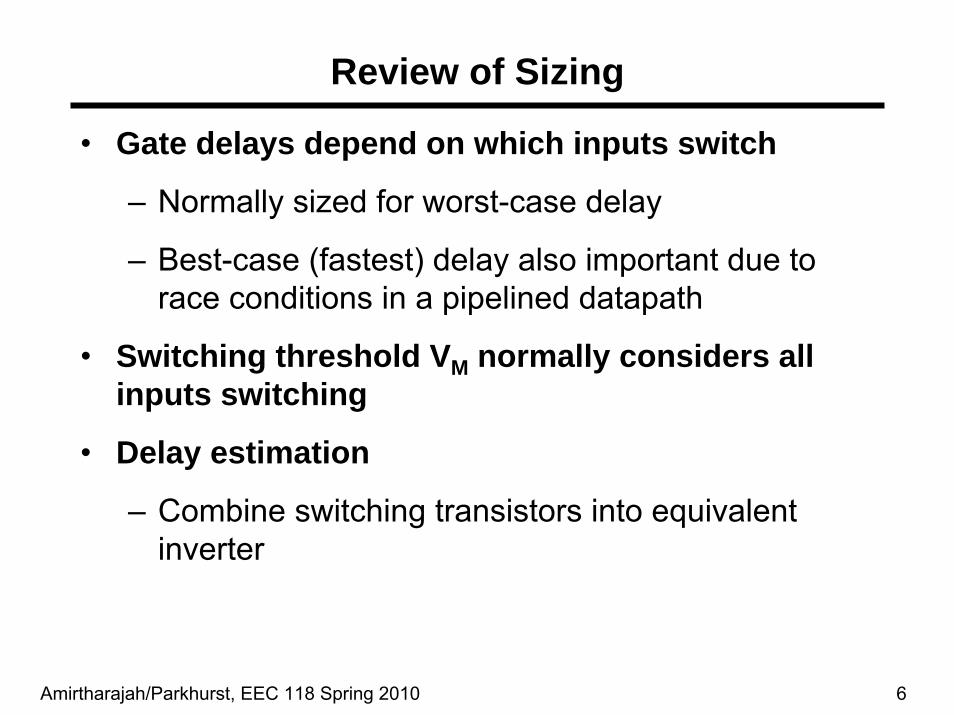
Review of Sizing
• Gate delays depend on which inputs switch
– Normally sized for worst-case delay
– Best-case (fastest) delay also important due to race conditions in a pipelined datapath
• Switching threshold VM normally considers all inputs switching
• Delay estimation
– Combine switching transistors into equivalent inverter
Amirtharajah/Parkhurst, EEC 118 Spring 2010 7
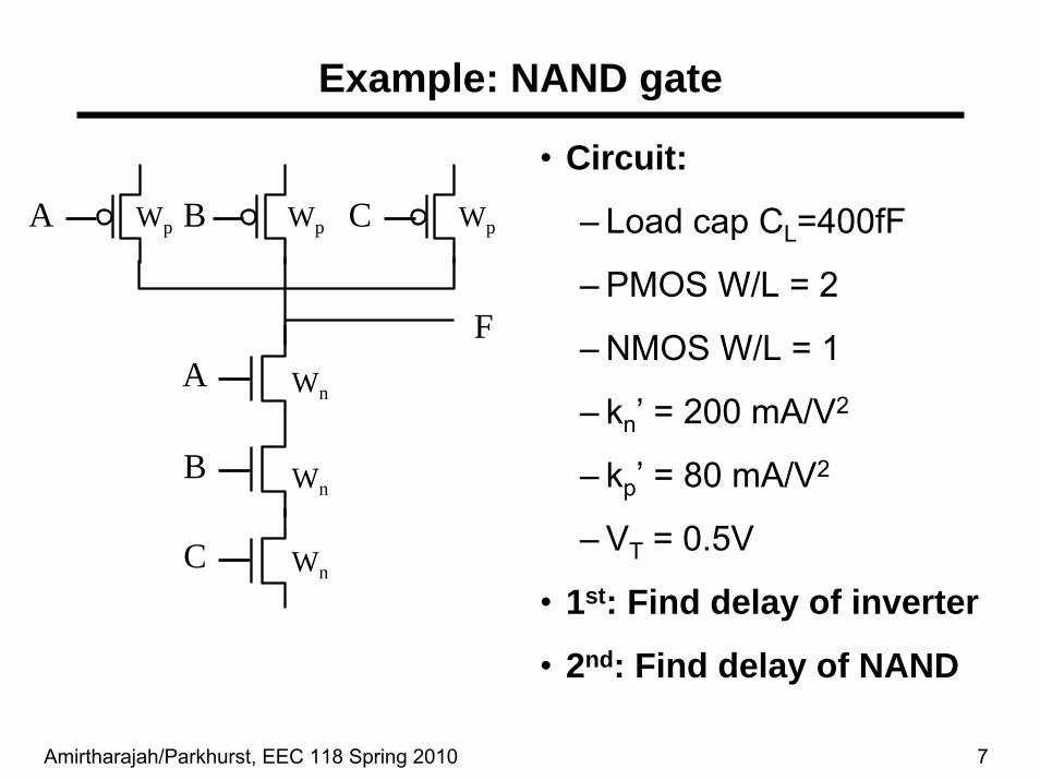
Example: NAND gate
• Circuit:
– Load cap CL=400fF
– PMOS W/L = 2
– NMOS W/L = 1
– kn’ = 200 mA/V2
– kp’ = 80 mA/V2
– VT = 0.5V
• 1st: Find delay of inverter
• 2nd: Find delay of NAND
AF
Wn
Wp
B
C
A WpB WpC
Wn
Wn
Amirtharajah/Parkhurst, EEC 118 Spring 2010 8
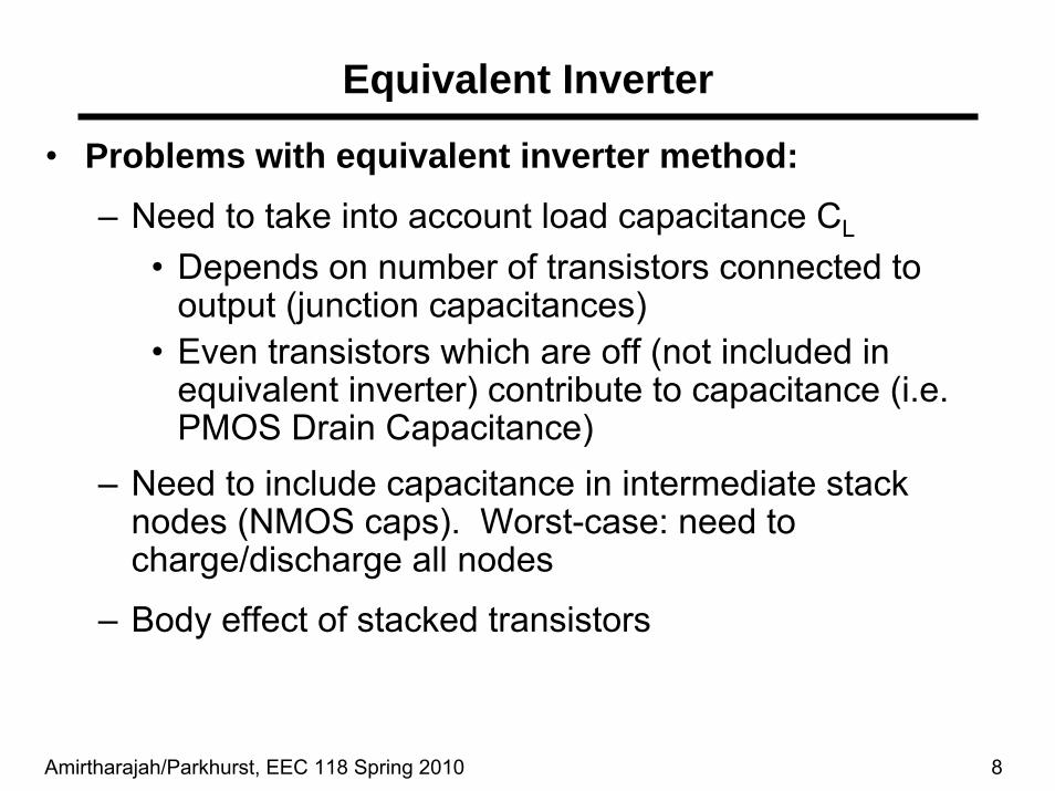
Equivalent Inverter
• Problems with equivalent inverter method:– Need to take into account load capacitance CL
• Depends on number of transistors connected to output (junction capacitances)
• Even transistors which are off (not included in equivalent inverter) contribute to capacitance (i.e. PMOS Drain Capacitance)
– Need to include capacitance in intermediate stack nodes (NMOS caps). Worst-case: need to charge/discharge all nodes
– Body effect of stacked transistors

Amirtharajah/Parkhurst, EEC 118 Spring 2010 9
Load Capacitance• Output capacitance includes junction caps of all
transistors on output
• Reducing load capacitance
– Minimize number of transistors on output node
– Tapering transistor stacks:• Wider transistors closest to power and ground nodes,
narrower at output• Transistors closest to power nodes carry more current

Amirtharajah/Parkhurst, EEC 118 Spring 2010 10
Intermediate Node Capacitances
• Internal capacitances in CMOS gates are charged and discharged– Depends on input pattern
– Increases delay of gate
• Simple analysis– Combine internal capacitances into output load
– Assumes all capacitances charged and discharged fully
• Effect on delay analysis– Gate delay depends on timing of inputs!
Amirtharajah/Parkhurst, EEC 118 Spring 2010 11
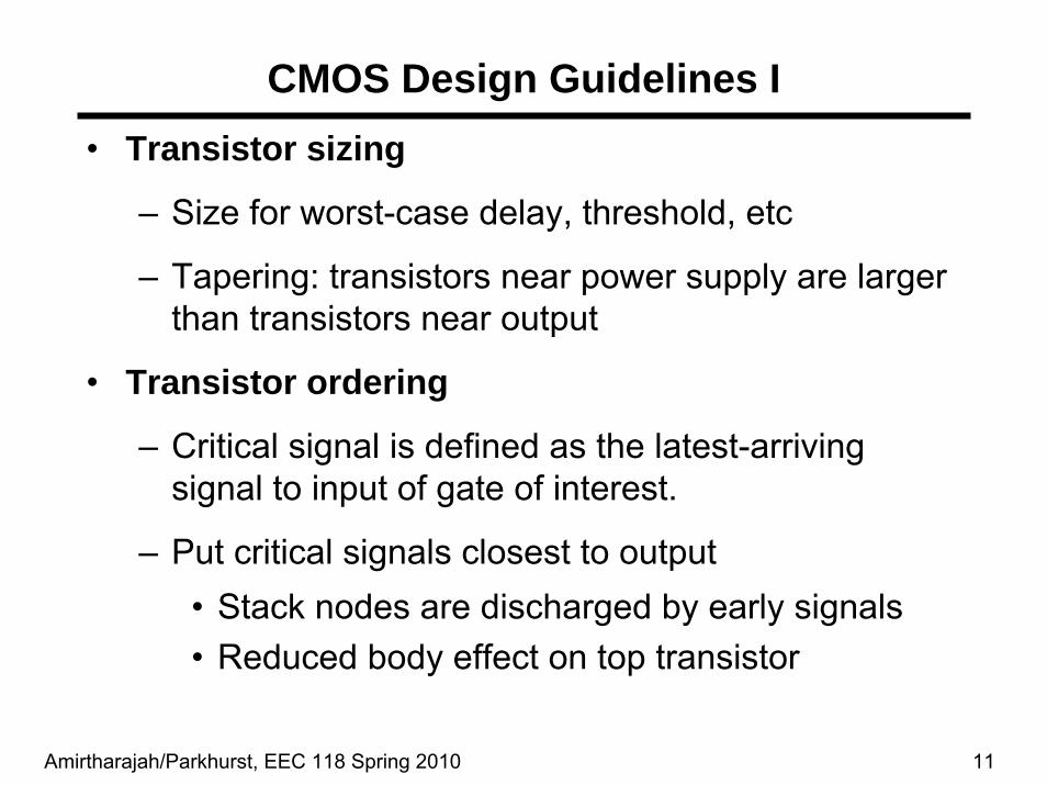
CMOS Design Guidelines I• Transistor sizing
– Size for worst-case delay, threshold, etc
– Tapering: transistors near power supply are larger than transistors near output
• Transistor ordering
– Critical signal is defined as the latest-arriving signal to input of gate of interest.
– Put critical signals closest to output• Stack nodes are discharged by early signals• Reduced body effect on top transistor

Amirtharajah/Parkhurst, EEC 118 Spring 2010 12
CMOS Design Guidelines II• Limit fan-in of gate
– Fan-in: number of gate inputs– Affects size of transistor stacks– Normally fan-in limit is 3-4
• Convert large multi-input gates into smaller chain of gates
• Limit fanout of gate– Fanout: number of gates connected to output– Capacitive load: affects gate delay
• NANDs are better than NORs– Series NMOS devices less area, capacitance than
equivalent series PMOS devices
Amirtharajah/Parkhurst, EEC 118 Spring 2010 13
CMOS Disadvantages• For N-input CMOS gate, 2N transistors required
– Each input connects to an NMOS and PMOS transistor
– Large input capacitance: limits fanout
• Large fan-in gates: always have long transistor stack in PUN or PDN– Limits pullup or pulldown delay
– Requires very large transistors
• Single-stage gates are inverting
Amirtharajah/Parkhurst, EEC 118 Spring 2010 14
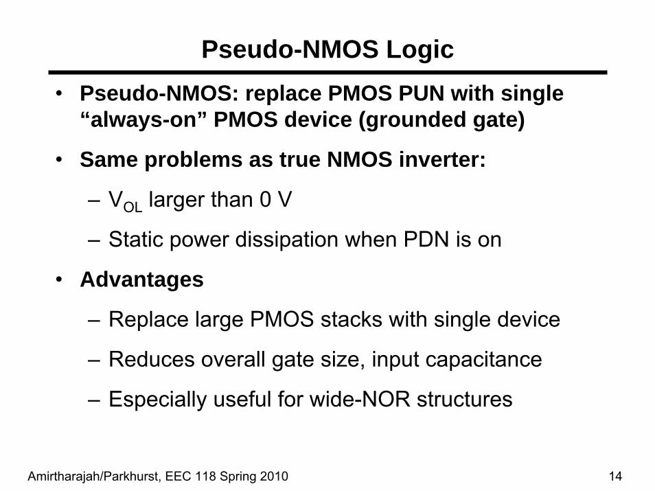
Pseudo-NMOS Logic• Pseudo-NMOS: replace PMOS PUN with single
“always-on” PMOS device (grounded gate)
• Same problems as true NMOS inverter:
– VOL larger than 0 V
– Static power dissipation when PDN is on
• Advantages
– Replace large PMOS stacks with single device
– Reduces overall gate size, input capacitance
– Especially useful for wide-NOR structures
Amirtharajah/Parkhurst, EEC 118 Spring 2010 15
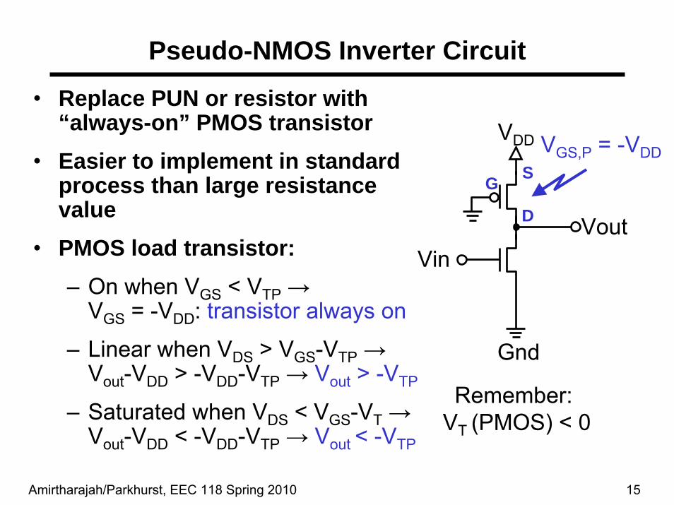
Pseudo-NMOS Inverter Circuit
• Replace PUN or resistor with “always-on” PMOS transistor
• Easier to implement in standard process than large resistance value
• PMOS load transistor:– On when VGS < VTP →
VGS = -VDD: transistor always on
– Linear when VDS > VGS-VTP →Vout-VDD > -VDD-VTP → Vout > -VTP
– Saturated when VDS < VGS-VT →Vout-VDD < -VDD-VTP → Vout < -VTP
Vin
VDD
Gnd
G S
D
VGS,P = -VDD
Vout
Remember: VT (PMOS) < 0
Amirtharajah/Parkhurst, EEC 118 Spring 2010 16
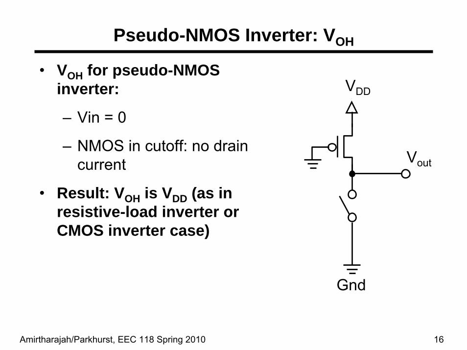
Pseudo-NMOS Inverter: VOH
• VOH for pseudo-NMOS inverter:
– Vin = 0
– NMOS in cutoff: no drain current
• Result: VOH is VDD (as in resistive-load inverter or CMOS inverter case)
VDD
Gnd
Vout
Amirtharajah/Parkhurst, EEC 118 Spring 2010 17
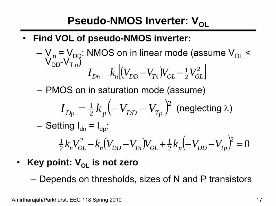
Pseudo-NMOS Inverter: VOL
• Find VOL of pseudo-NMOS inverter: – Vin = VDD: NMOS on in linear mode (assume VOL <
VDD-VT,n) ( )[ ]221
OLOLTnDDnDn VVVVkI −−=
– PMOS on in saturation mode (assume)
( )221
TpDDpDp VVkI −−= (neglecting λ)
– Setting Idn = Idp:
( ) ( ) 02212
21 =−−+−− TpDDpOLTnDDnOLn VVkVVVkVk
• Key point: VOL is not zero
– Depends on thresholds, sizes of N and P transistors

Amirtharajah/Parkhurst, EEC 118 Spring 2010 18
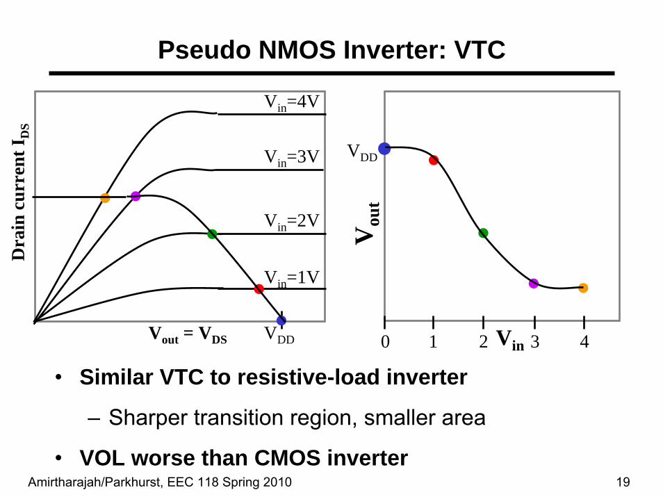
Pseudo NMOS Inverter: I/V Curves
VDS = Vout
Dra
in c
urre
nt I D
S
Vin=2V
VDD
Vin=1V
Vin=3V
Vin=4V
-VDS = -(Vout - VDD)-D
rain
cur
rent
-ID
S
I/V curve for NMOS: I/V curve for PMOS:
VGS=-VDD
• Plot of -IDS vs -VDS since current is from source to drain• Only one curve since VGSfixed
Amirtharajah/Parkhurst, EEC 118 Spring 2010 19
Vout = VDS
Dra
in c
urre
nt I D
S
Vin=2V
VDD
Vin=1V
Vin=3V
Vin=4V
Vou
t
Vin1 2 3 40
VDD
• Similar VTC to resistive-load inverter
– Sharper transition region, smaller area
• VOL worse than CMOS inverter
Pseudo NMOS Inverter: VTC
Amirtharajah/Parkhurst, EEC 118 Spring 2010 20
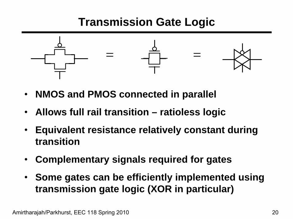
Transmission Gate Logic
• NMOS and PMOS connected in parallel
• Allows full rail transition – ratioless logic
• Equivalent resistance relatively constant during transition
• Complementary signals required for gates
• Some gates can be efficiently implemented using transmission gate logic (XOR in particular)
= =
Amirtharajah/Parkhurst, EEC 118 Spring 2010 21
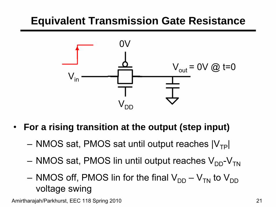
Equivalent Transmission Gate Resistance
• For a rising transition at the output (step input)
– NMOS sat, PMOS sat until output reaches |VTP|
– NMOS sat, PMOS lin until output reaches VDD-VTN
– NMOS off, PMOS lin for the final VDD – VTN to VDDvoltage swing
Vin
Vout = 0V @ t=0
VDD
0V
Amirtharajah/Parkhurst, EEC 118 Spring 2010 22
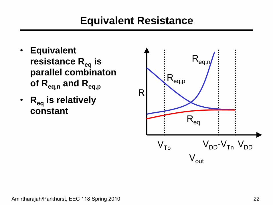
Equivalent Resistance
• Equivalent resistance Req is parallel combinatonof Req,n and Req,p
• Req is relatively constant
VDDVTp VDD-VTn
Req,p
Req,n
Req
R
Vout
Amirtharajah/Parkhurst, EEC 118 Spring 2010 23
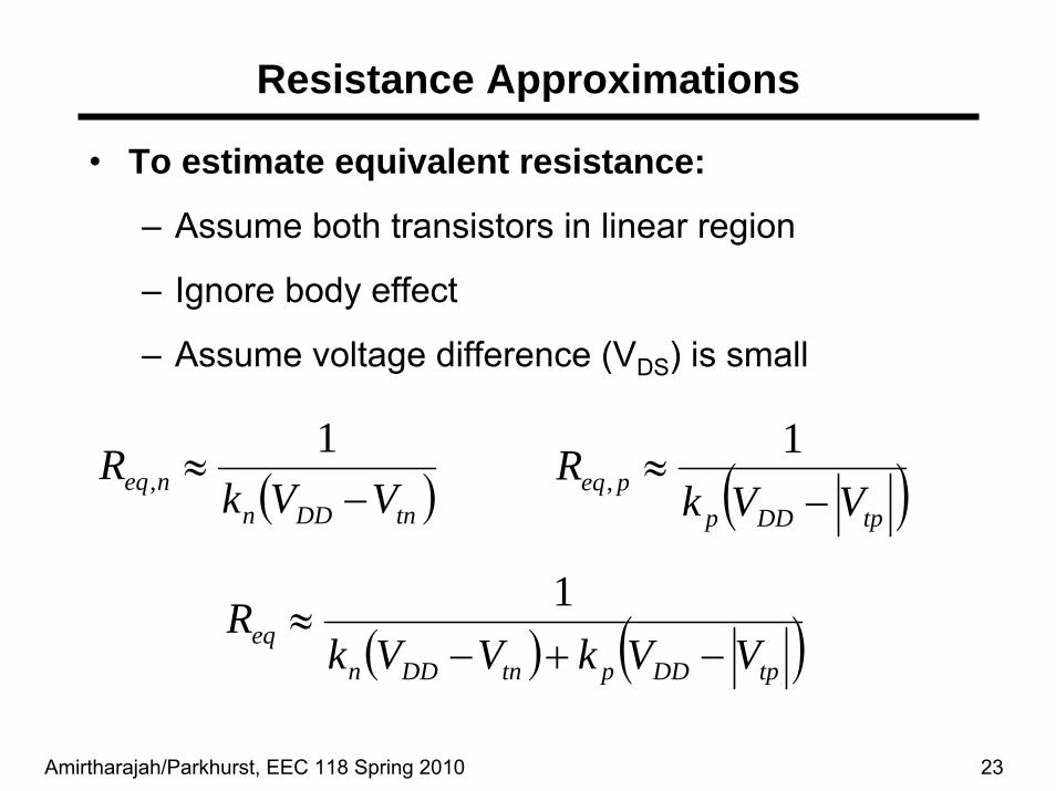
Resistance Approximations
• To estimate equivalent resistance:
– Assume both transistors in linear region
– Ignore body effect
– Assume voltage difference (VDS) is small
( )tnDDnneq VVk
R−
≈1
, ( )tpDDppeq VVk
R−
≈1
,
( ) ( )tpDDptnDDneq VVkVVk
R−+−
≈1
Amirtharajah/Parkhurst, EEC 118 Spring 2010 24
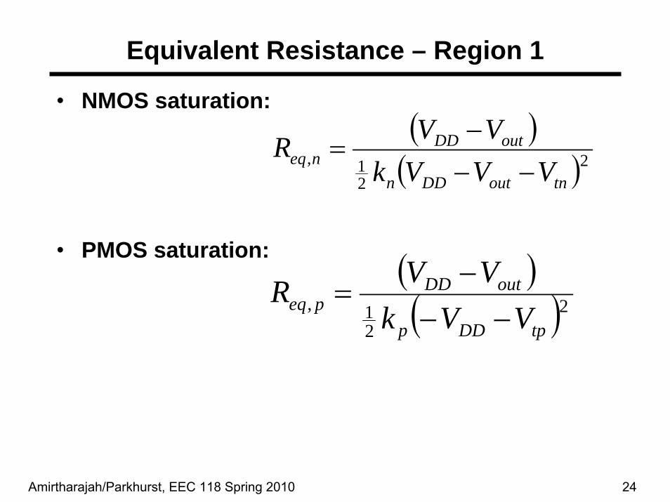
Equivalent Resistance – Region 1
• NMOS saturation:
• PMOS saturation:
( )( )22
1,tnoutDDn
outDDneq VVVk
VVR−−
−=
( )( )22
1,tpDDp
outDDpeq VVk
VVR−−
−=
Amirtharajah/Parkhurst, EEC 118 Spring 2010 25
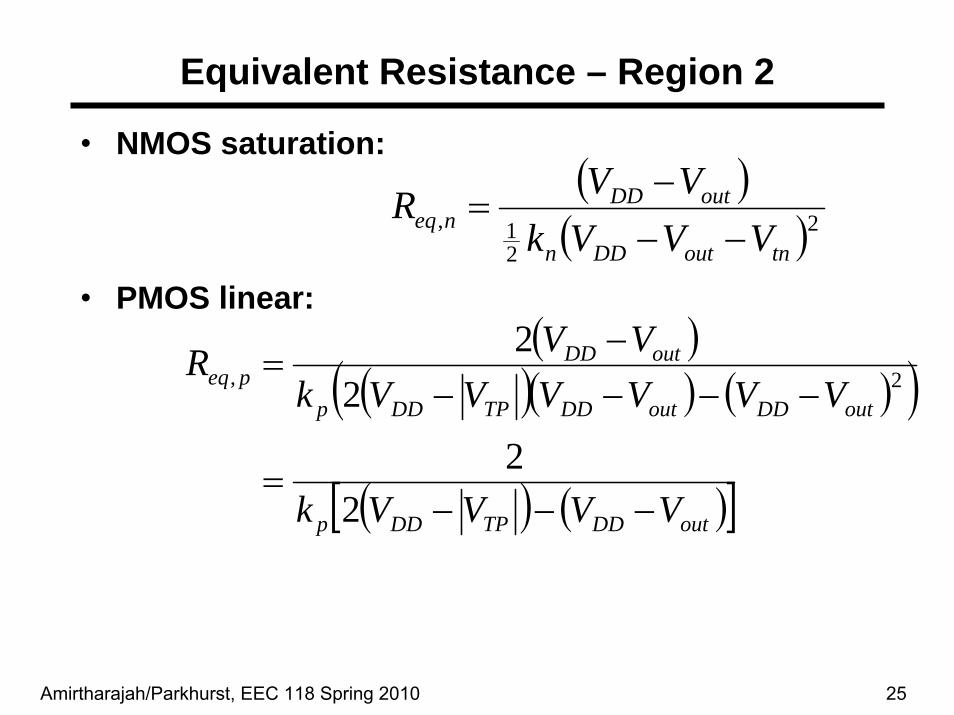
Equivalent Resistance – Region 2
• NMOS saturation:
• PMOS linear:( )
( )( ) ( )( )
( ) ( )[ ]outDDTPDDp
outDDoutDDTPDDp
outDDpeq
VVVVk
VVVVVVkVVR
−−−=
−−−−−
=
22
22
2,
( )( )22
1,tnoutDDn
outDDneq VVVk
VVR−−
−=
Amirtharajah/Parkhurst, EEC 118 Spring 2010 26
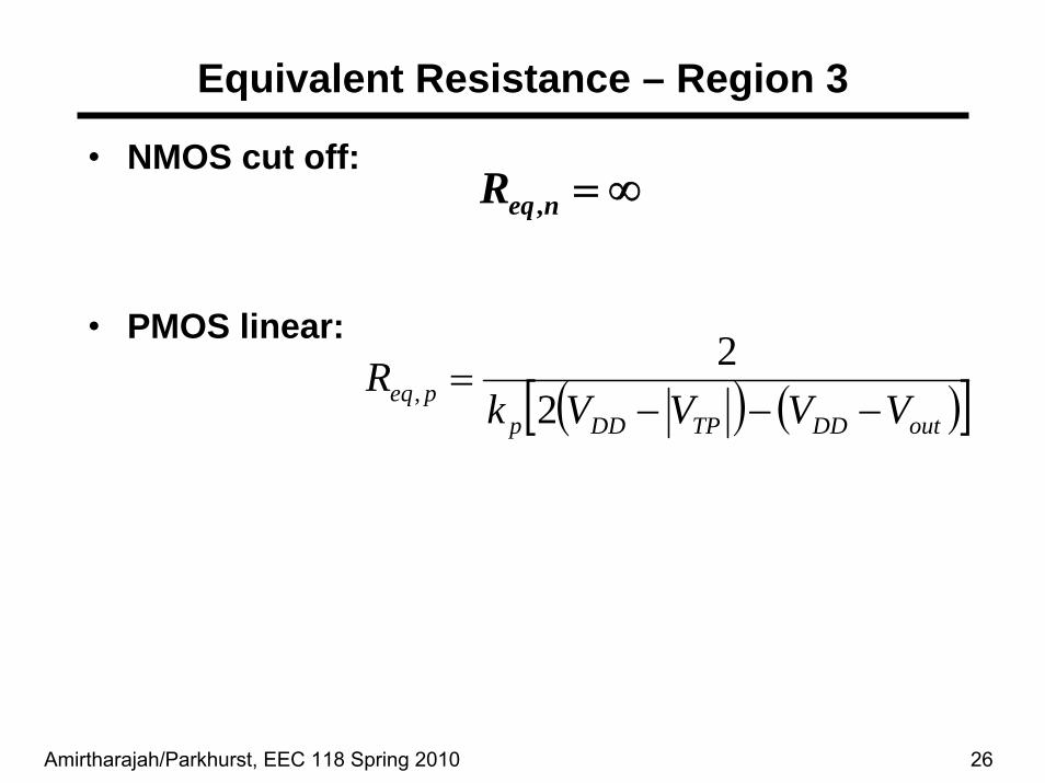
Equivalent Resistance – Region 3
• NMOS cut off:
• PMOS linear:
∞=neqR ,
( ) ( )[ ]outDDTPDDppeq VVVVk
R−−−
=2
2,
Amirtharajah/Parkhurst, EEC 118 Spring 2010 27
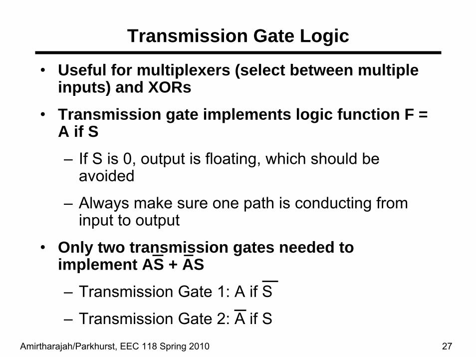
Transmission Gate Logic
• Useful for multiplexers (select between multiple inputs) and XORs
• Transmission gate implements logic function F = A if S– If S is 0, output is floating, which should be
avoided
– Always make sure one path is conducting from input to output
• Only two transmission gates needed to implement AS + AS– Transmission Gate 1: A if S
– Transmission Gate 2: A if S
Amirtharajah/Parkhurst, EEC 118 Spring 2010 28
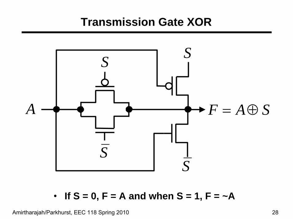
• If S = 0, F = A and when S = 1, F = ~A
Transmission Gate XOR
S
S
A
S
S
SAF ⊕=
Amirtharajah/Parkhurst, EEC 118 Spring 2010 29
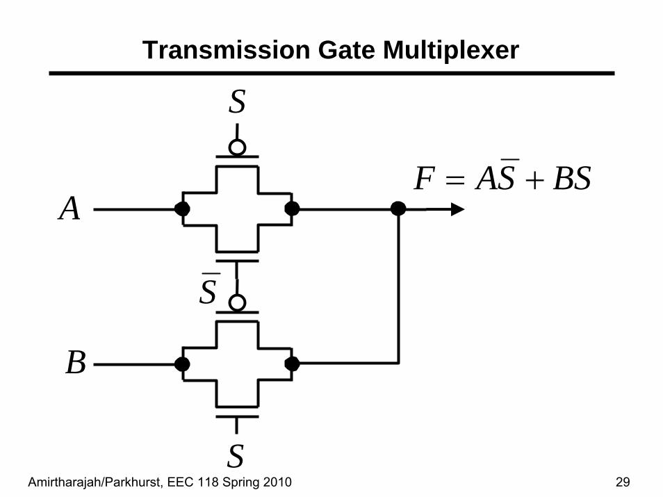
Transmission Gate Multiplexer
S
S
A
S
BSSAF +=
B

Amirtharajah/Parkhurst, EEC 118 Spring 2010 30
• PMOS devices in parallel with NMOS transistors pass full VDD (only one logic path shown above)
• Requires more devices, but each can be sized smaller than static CMOS
• Output inverter reduces impact of fanout
Full Transmission Gate LogicB C
A
B C
BCAF =

Amirtharajah/Parkhurst, EEC 118 Spring 2010 31
Next Topic: Dynamic Circuits
• Extend dynamic sequential circuit idea to logic circuits
– Improved speed
– Reduced area
– Challenging to design: timing and noise issues, charge sharing, leakage
– Preferred design style for high performance circuits


