
1 of 71GS1559 HD-LINX™ II Multi-Rate Deserializer with Loop-Through Cable DriverData Sheet30572 - 8 July 2008
GS1559 HD-LINX™ II Multi-Rate Deserializer with Loop-Through Cable Driver
www.gennum.com
Key Features• SMPTE 292M and SMPTE 259M-C compliant
descrambling and NRZI → NRZ decoding (with bypass)
• DVB-ASI 8b/10b decoding
• Auto-configuration for HD-SDI and SD-SDI
• Serial loop-through Cable Driver output selectable as reclocked or non-reclocked
• Dual serial digital input buffers with 2 x 1 mux
• Integrated serial digital signal termination
• Integrated Reclocker
• Automatic or Manual rate selection/indication (HD/SD)
• Descrambler Bypass option
• User selectable additional processing features including:
• CRC, TRS, ANC data checksum, line number and EDH CRC error detection and correction
• Programmable ANC data detection• Illegal code remapping
• Internal Flywheel for noise immune H, V, F extraction
• FIFO load Pulse
• 20-bit/10-bit CMOS parallel output data bus
• 148.5MHz / 74.25MHz / 27MHz / 13.5MHz parallel digital output
• Automatic standards detection and indication
• 1.8V core Power Supply and 3.3V Charge Pump Power Supply
• 3.3V digital I/O supply
• JTAG test interface
• Available in a Pb-free package
• Small footprint (11mm x 11mm)
Applications• SMPTE 292M Serial Digital Interfaces
• SMPTE 259M-C Serial Digital Interfaces
• DVB-ASI Serial Digital Interfaces
DescriptionThe GS1559 is a reclocking Deserializer with a serial loop-through Cable Driver. When used in conjunction with the GS1574 Automatic Cable Equalizer and the GO1555/GO1525* Voltage Controlled Oscillator, a receive solution can be realized for HD-SDI, SD-SDI and DVB-ASI applications.
In addition to reclocking and deserializing the input data stream, the GS1559 performs NRZI-to-NRZ decoding, descrambling as per SMPTE 292M/259M-C, and word alignment when operating in SMPTE mode. When operating in DVB-ASI mode, the device will word align the data to K28.5 sync characters and 8b/10b decode the received stream.
Two serial digital input buffers are provided with a 2x1 Multiplexer to allow the device to select from one of two serial digital input signals.
The Integrated Reclocker features a very wide Input Jitter Tolerance of ±0.3 UI (total 0.6 UI), a rapid asynchronous lock time, and full compliance with DVB-ASI data streams.
An integrated Cable Driver is provided for serial input loop-through applications and can be selected to output either buffered or reclocked data. This Cable Driver also features an output mute on loss of signal, high-impedance mode, adjustable signal swing, and automatic dual slew-rate selection depending on HD/SD operational requirements.
The GS1559 also includes a range of data processing functions such as error detection and correction, automatic standards detection, and EDH support. The device can also detect and extract SMPTE 352M payload identifier packets and independently identify the received video standard. This information is read from internal registers via the Host Interface port.
Line-based CRC errors, line number errors, TRS errors, EDH CRC errors and ancillary data checksum errors can all be detected. A single ‘DATA_ERROR’ pin is provided which is a logical 'OR'ing of all detectable errors. Individual error status is stored in internal ‘ERROR_STATUS’ registers.
Finally, the device can correct detected errors and insert new TRS ID words, line-based CRC words, ancillary data checksum words, EDH CRC words, and line numbers. Illegal code re-mapping is also available. All processing functions may be individually enabled or disabled via Host Interface control.
GS1559 HD-LINX™ II Multi-Rate Deserializer with Loop-Through Cable DriverData Sheet30572 - 8 July 2008
2 of 71
*For new designs use the GO1555.
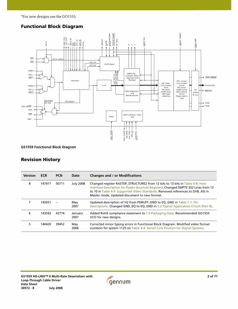
Functional Block Diagram
GS1559 Functional Block Diagram
Revision History
Version ECR PCN Date Changes and / or Modifications
8 147971 50711 July 2008 Changed register RASTER_STRUCTURE2 from 12 bits to 13 bits in Table 4-8: Host Interface Description for Raster Structure Registers. Changed SMPTE 352 Lines from 13 to 10 in Table 4-9: Supported Video Standards. Removed references to DVB_ASI in Master mode. Updated document to new format.
7 145031 – May 2007
Updated description of H2 from PDBUFF_GND to EQ_GND in Table 1-1: Pin Descriptions. Changed GND_EQ to EQ_GND in 5.2 Typical Application Circuit (Part B).
6 143592 42774 January 2007
Added RoHS compliance statement to 7.3 Packaging Data. Recommended GO1555 VCO for new designs.
5 140420 39452 May 2006
Corrected minor typing errors in Functional Block Diagram. Modified video format numbers for system 1125 on Table 4-4: Switch Line Position for Digital Systems.
DDI_1
TERM 1
TERM 2
DDI_1
DDI_2
DDI_2
Reclocker
SDO
SDO
SDO_EN/DIS
RSET
S->P
SMPTE De-scramble, Wordalignment and
flywheel
H V F
DOUT[19:0]
IP_SEL
carrier_detect
RC
_BY
P
(o/p mute)pll_lock
RESET_TR
ST
asi_sync_d
et
HOST Interface / JTAGtest
CS_TM
SSC
LK_TC
KSD
IN_TD
ISD
OU
T_TDO
FIFO_LD
DATA_ERROR
YANC
CANC
Reset
JTAG
/HO
ST
IOPR
OC
_EN/D
IS
CRC checkLine number
checkTRS check
CSUM checkANC datadetection
Word alignmentand
8b/10b decode
CRC correctLine number
correctTRS correct
CSUM correctEDH check &
correctIllegal code re-
map
20bit/10b
it
I/O
Buffer& mux
FW_EN
/DIS
CP_C
AP
DV
B_A
SI
pll_lock
VC
OV
CO
LFLB
_CO
NT
VC
O_V
CC
VC
O_G
ND
SD/H
D
MA
STER/SLA
VE
PCLK
LOC
KED
LOCK detect
CD1
CD2
SMPTE_B
YPA
SS
smp
te_sync_d
et
rclk_ctrl
rclk_bypass

Contents
Key Features ........................................................................................................................................................1
Applications.........................................................................................................................................................1
Description...........................................................................................................................................................1
Functional Block Diagram ..............................................................................................................................2
Revision History .................................................................................................................................................2
1. Pin Out..............................................................................................................................................................5
1.1 Pin Assignment..................................................................................................................................5
1.2 Pin Descriptions ................................................................................................................................6
2. Electrical Characteristics ........................................................................................................................ 16
2.1 Absolute Maximum Ratings....................................................................................................... 16
2.2 DC Electrical Characteristics ..................................................................................................... 16
2.3 AC Electrical Characteristics ..................................................................................................... 18
3. Input/Output Circuits .............................................................................................................................. 20
3.1 Host Interface Map........................................................................................................................ 22
3.1.1 Host Interface Map (R/W Configurable Registers) ................................................ 23
3.1.2 Host Interface Map (Read Only Registers) ............................................................... 24
4. Detailed Description................................................................................................................................. 25
4.1 Functional Overview.................................................................................................................... 25
4.2 Serial Digital Input ........................................................................................................................ 25
4.2.1 Input Signal Selection ..................................................................................................... 25
4.2.2 Carrier Detect Input......................................................................................................... 26
4.2.3 Single Input Configuration............................................................................................ 26
4.3 Serial Digital Reclocker ............................................................................................................... 26
4.3.1 External VCO ..................................................................................................................... 26
4.3.2 Loop Bandwidth................................................................................................................ 27
4.4 Serial Digital Loop-Through Output........................................................................................ 27
4.4.1 Output Swing ..................................................................................................................... 27
4.4.2 Reclocker Bypass Control .............................................................................................. 28
4.4.3 Serial Digital Output Mute............................................................................................. 28
4.5 Serial-To-Parallel Conversion ................................................................................................... 29
4.6 Modes Of Operation ..................................................................................................................... 29
4.6.1 Lock Detect ......................................................................................................................... 29
4.6.2 Master Mode....................................................................................................................... 30
4.6.3 Slave Mode.......................................................................................................................... 31
4.7 SMPTE Functionality .................................................................................................................... 31
4.7.1 SMPTE Descrambling and Word Alignment ........................................................... 32
4.7.2 Internal Flywheel ............................................................................................................. 32
4.7.3 Switch Line Lock Handling............................................................................................ 33
4.7.4 HVF Timing Signal Generation .................................................................................... 36
4.8 DVB-ASI Functionality ................................................................................................................ 38
4.8.1 DVB-ASI 8b/10b Decoding and Word Alignment................................................. 38
4.8.2 Status Signal Outputs ...................................................................................................... 38
GS1559 HD-LINX™ II Multi-Rate Deserializer with Loop-Through Cable DriverData Sheet30572 - 8 July 2008
3 of 71

4.9 Data Through Mode ...................................................................................................................... 39
4.10 Additional Processing Functions ........................................................................................... 39
4.10.1 FIFO Load Pulse .............................................................................................................. 39
4.10.2 Ancillary Data Detection and Indication ............................................................... 40
4.10.3 SMPTE 352M Payload Identifier ............................................................................... 43
4.10.4 Automatic Video Standard and Data Format Detection................................... 44
4.10.5 Error Detection and Indication.................................................................................. 47
4.10.6 Error Correction and Insertion .................................................................................. 53
4.10.7 EDH Flag Detection ....................................................................................................... 55
4.11 Parallel Data Outputs................................................................................................................. 57
4.11.1 Parallel Data Bus Buffers ............................................................................................. 57
4.11.2 Parallel Output in SMPTE Mode................................................................................ 58
4.11.3 Parallel Output in DVB-ASI Mode............................................................................ 58
4.11.4 Parallel Output in Data-Through Mode.................................................................. 59
4.11.5 Parallel Output Clock (PCLK) ..................................................................................... 59
4.12 GSPI Host Interface..................................................................................................................... 60
4.12.1 Command Word Description ..................................................................................... 61
4.12.2 Data Read and Write Timing ...................................................................................... 61
4.12.3 Configuration and Status Registers.......................................................................... 62
4.13 JTAG................................................................................................................................................. 63
4.14 Device Power Up......................................................................................................................... 64
4.15 Device Reset.................................................................................................................................. 64
5. Application Reference Design .............................................................................................................. 65
5.1 Typical Application Circuit (Part A)......................................................................................... 65
5.2 Typical Application Circuit (Part B) ......................................................................................... 66
6. References & Relevant Standards ........................................................................................................ 67
7. Package & Ordering Information ......................................................................................................... 68
7.1 Package Dimensions..................................................................................................................... 68
7.2 Solder Reflow Profiles.................................................................................................................. 69
7.3 Packaging Data............................................................................................................................... 70
7.4 Ordering Information................................................................................................................... 70
GS1559 HD-LINX™ II Multi-Rate Deserializer with Loop-Through Cable DriverData Sheet30572 - 8 July 2008
4 of 71
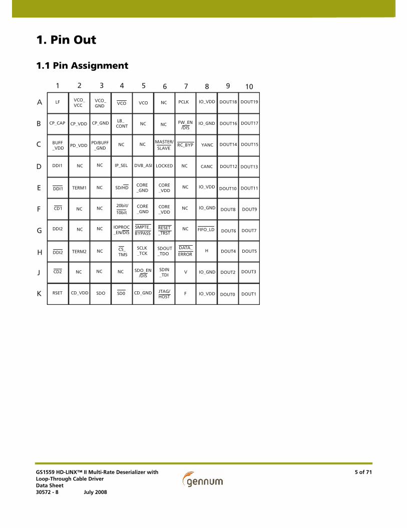
1. Pin Out
1.1 Pin Assignment
1 32 4 5 6 7 8 9 10
A
B
C
D
E
F
G
H
J
K
LOCKED
PCLK
LB_CONT
NC
RC_BYP
DOUT19DOUT18
DOUT17DOUT16
DOUT14
DOUT12
DOUT10
DOUT8
DOUT6
DOUT4
DOUT2
DOUT1
DOUT15
DOUT13
DOUT11
DOUT9
DOUT7
DOUT5
DOUT3
DOUT0JTAG/HOST
SD/HD
IO_VDD
IO_VDD
IO_GND
FIFO_LD
H
IO_VDD
CORE_VDD
IO_GND
CORE_VDD
CORE_GND
CORE_GND
DATA_
ERROR
FW_EN/DIS
DVB_ASI
SMPTE_BYPASS
MASTER/SLAVE
NC
NC20bit/
10bit
SDIN_TDI
SCLK_TCK
SDOUT_TDO
CS_TMS
RESET_TRST
NC
NC
NC
CD_VDD
SDO_EN/DIS
IOPROC_EN/DIS
RSET
NC
NC NC NC
BUFF_VDD
NC
NCNCNC
NCCD1
CP_CAP
TERM1
DDI1
DDI1
DDI2
DDI2 TERM2
SDO SD0
VCO_VCC
VCO_GND
LF VCOVCO
CP_VDD CP_GND
PD_VDDPD/BUFF
_GNDYANC
IP_SEL CANC
NC
CD2 NC NC NC V IO_GND
CD_GND F
NC
GS1559 HD-LINX™ II Multi-Rate Deserializer with Loop-Through Cable DriverData Sheet30572 - 8 July 2008
5 of 71

1.2 Pin Descriptions
Table 1-1: Pin Descriptions
Pin Number
Name Timing Type Description
A1 LF Analog Output Control voltage to external Voltage Controlled Oscillator. Nominally +1.25V DC.
A2 VCO_VCC – Output Power
Power Supply for the external Voltage Controlled Oscillator. Connect to pin 7 of the GO1555/GO1525*. This pin is an output.
Should be isolated from all other power supplies.
*For new designs use the GO1555.
A3 VCO_GND – Output Power
Ground reference for the external Voltage Controlled Oscillator. Connect to pins 2, 4, 6, and 8 of the GO1555/GO1525*. This pin is an output.
Should be isolated from all other grounds.
*For new designs use the GO1555.
A4, A5 VCO, VCO Analog Input Differential inputs for the external VCO reference signal. For single ended devices such as the GO1555/GO1525*, VCO should be AC coupled to VCO_GND.
VCO is nominally 1.485GHz.
*For new designs use the GO1555.
A6, B5, B6, C4, C5, D2, D3, D7,
E3, E7, F2, F3, F7, G2,
G3, G7, H3, J2, J3,
J4,
NC – – No Connect.
A7 PCLK – Output PARALLEL DATA BUS CLOCK Signal levels are LVCMOS/LVTTL compatible.
HD 20-bit mode PCLK = 74.25MHz or 74.25/1.001MHz
HD 10-bit mode PCLK = 148.5MHz or 148.5/1.001MHz
SD 20-bit mode PCLK = 13.5MHz
SD 10-bit mode PCLK = 27MHz
A8, E8, K8 IO_VDD – Power Power Supply connection for digital I/O buffers. Connect to +3.3V DC digital.
GS1559 HD-LINX™ II Multi-Rate Deserializer with Loop-Through Cable DriverData Sheet30572 - 8 July 2008
6 of 71

A10, A9, B10, B9, C10, C9, D10, D9, E10, E9
DOUT[19:10] Synchronous with PCLK
Output PARALLEL DATA BUS Signal levels are LVCMOS/LVTTL compatible.
DOUT19 is the MSB and DOUT10 is the LSB.
HD 20-bit mode SD/HD = LOW 20bit/10bit = HIGH
Luma data output in SMPTE mode SMPTE_BYPASS = HIGH DVB_ASI = LOW
Data output in Data-Through mode SMPTE_BYPASS = LOW DVB_ASI = LOW
HD 10-bit mode SD/HD = LOW 20bit/10bit = LOW
Multiplexed Luma and Chroma data output in SMPTE mode SMPTE_BYPASS = HIGH DVB_ASI = LOW
Data output in Data-Through mode SMPTE_BYPASS = LOW DVB_ASI = LOW
SD 20-bit mode SD/HD = HIGH 20bit/10bit = HIGH
Luma data output in SMPTE mode SMPTE_BYPASS = HIGH DVB_ASI = LOW
Data output in Data-Through mode SMPTE_BYPASS = LOW DVB_ASI = LOW
DVB-ASI data in DVB-ASI mode SMPTE_BYPASS = LOW DVB_ASI = HIGH
SD 10-bit mode SD/HD = HIGH 20bit/10bit = LOW
Multiplexed Luma and Chroma data output in SMPTE mode SMPTE_BYPASS = HIGH DVB_ASI = LOW
Data input in data through mode SMPTE_BYPASS = LOW DVB_ASI = LOW
DVB-ASI data in DVB-ASI mode SMPTE_BYPASS = LOW DVB_ASI = HIGH
B1 CP_CAP Analog Input PLL lock time constant capacitor connection. Normally connected to VCO_GND through 2.2nF.
B2 CP_VDD – Power Power supply connection for the Charge Pump. Connect to +3.3V DC analog.
B3 CP_GND – Power Ground connection for the Charge Pump. Connect to analog GND.
B4 LB_CONT Analog Input Control voltage to set the loop bandwidth of the integrated Reclocker. Normally connected to VCO_GND through 40kΩ.
Table 1-1: Pin Descriptions (Continued)
Pin Number
Name Timing Type Description
GS1559 HD-LINX™ II Multi-Rate Deserializer with Loop-Through Cable DriverData Sheet30572 - 8 July 2008
7 of 71

B7 FW_EN/DIS Non Synchronous
Input CONTROL SIGNAL INPUT Signal levels are LVCMOS/LVTTL compatible.
Used to enable or disable the noise immune Flywheel of the device.
When set HIGH, the internal Flywheel is enabled. This Flywheel is used in the extraction and generation of TRS timing signals, in automatic video standards detection, and in manual switch line lock handling.
When set LOW, the internal Flywheel is disabled and TRS correction and insertion is unavailable.
B8, F8, J8 IO_GND – Power Ground connection for digital I/O buffers. Connect to digital GND.
C1 BUFF_VDD – Power Power Supply connection for the Serial Digital Input buffers. Connect to +1.8V DC analog.
C2 PD_VDD – Power Power Supply connection for the Phase Detector. Connect to +1.8V DC analog.
C3 PDBUFF_GND – Power Ground connection for the Phase Detector and Serial Digital Input buffers. Connect to analog GND.
C6 MASTER/SLAVE Non Synchronous
Input CONTROL SIGNAL INPUT Signal levels are LVCMOS/LVTTL compatible.
Used to determine the input / output selection for the DVB_ASI, SD/HD, RC_BYP and SMPTE_BYPASS pins.
When set HIGH, the GS1559 is set to operate in Master mode where SD/HD, RC_BYP and SMPTE_BYPASS become status signal output pins set by the device. In this mode, the GS1559 will automatically detect, reclock, deserialize and process SD SMPTE and HD SMPTE input data.
When set LOW, the GS1559 is set to operate in Slave mode where DVB_ASI, SD/HD, RC_BYP and SMPTE_BYPASS become control signal input pins. In this mode, the application layer must set these external device pins for the correct reception of either SMPTE or DVB-ASI data. Slave mode also supports the reclocking and deserializing of data not conforming to SMPTE or DVB-ASI streams.
C7 RC_BYP Non Synchronous
Input /Output
CONTROL SIGNAL INPUT / STATUS SIGNAL OUTPUT Signal levels are LVCMOS/LVTTL compatible.
This pin will be an input set by the application layer in Slave mode, and will be an output set by the device in Master mode.
Master mode (MASTER/SLAVE = HIGH) The RC_BYP signal will be HIGH only when the device has successfully locked to a SMPTE compliant input data stream. In this case, the serial digital loop-through output will be a reclocked version of the input.
The RC_BYP signal will be LOW whenever the input does not conform to a SMPTE compliant data stream. In this case, the serial digital loop-through output will be a buffered version of the input.
Slave mode (MASTER/SLAVE = LOW) When set HIGH, the serial digital output will be a reclocked version of the input signal regardless of whether the device is in SMPTE, DVB-ASI or Data-Through mode.
When set LOW, the serial digital output will be a buffered version of the input signal in all modes.
Table 1-1: Pin Descriptions (Continued)
Pin Number
Name Timing Type Description
GS1559 HD-LINX™ II Multi-Rate Deserializer with Loop-Through Cable DriverData Sheet30572 - 8 July 2008
8 of 71
C8 YANC Synchronous with PCLK
Output STATUS SIGNAL OUTPUT Signal levels are LVCMOS/LVTTL compatible.
Used to indicate the presence of ancillary data in the video stream.
HD Mode (SD/HD = LOW) The YANC signal will be HIGH when the device has detected VANC or HANC data in the luma video stream and LOW otherwise.
SD Mode (SD/HD = LOW) For 20-bit demultiplexed data (20bit/10bit = HIGH), the YANC signal will be HIGH when VANC or HANC data is detected in the Luma video stream and LOW otherwise.
For 10-bit multiplexed data (20bit/10bit = LOW), the YANC signal will be HIGH when VANC or HANC data is detected anywhere in the data stream and LOW otherwise.
D1, E1 DDI1, DDI1 Analog Input Differential input pair for serial digital input 1.
D4 IP_SEL Non Synchronous
Input CONTROL SIGNAL INPUT Signal levels are LVCMOS/LVTTL compatible.
Used to select DDI1 / DDI1 or DDI2 / DDI2 as the Serial Digital Input signal, and CD1 or CD2 as the Carrier Detect input signal.
When set HIGH, DDI1 / DDI1 is selected as the Serial Digital Input and CD1 is selected as the Carrier Detect input signal.
When set LOW, DDI2 / DDI2 Serial Digital Input and CD2 Carrier Detect input signal is selected.
D5 DVB_ASI Non Synchronous
Input / Output
CONTROL SIGNAL INPUT / STATUS SIGNAL OUTPUT Signal levels are LVCMOS/LVTTL compatible.
This pin will be an input set by the application layer in Slave mode.
This pin and its function are not supported in Master mode.
Slave mode (MASTER/SLAVE = LOW) When set HIGH in conjunction with SD/HD = HIGH and SMPTE_BYPASS = LOW, the device will be configured to operate in DVB-ASI mode.
When set LOW, the device will not support the decoding or word alignment of received DVB-ASI data.
D6 LOCKED Synchronous with PCLK
Output STATUS SIGNAL OUTPUT Signal levels are LVCMOS / LVTTL compatible.
The LOCKED signal will be HIGH whenever the device has correctly received and locked to SMPTE compliant data in SMPTE mode or DVB-ASI compliant data in DVB-ASI mode.
It will be LOW otherwise.
Table 1-1: Pin Descriptions (Continued)
Pin Number
Name Timing Type Description
GS1559 HD-LINX™ II Multi-Rate Deserializer with Loop-Through Cable DriverData Sheet30572 - 8 July 2008
9 of 71
D8 CANC Synchronous with PCLK
Output STATUS SIGNAL OUTPUT Signal levels are LVCMOS/LVTTL compatible.
Used to indicate the presence of ancillary data in the video stream.
HD Mode (SD/HD = LOW) The CANC signal will be HIGH when the device has detected VANC or HANC data in the chroma video stream and LOW otherwise.
SD Mode (SD/HD = LOW) For 20-bit demultiplexed data (20bit/10bit = HIGH), the CANC signal will be HIGH when VANC or HANC data is detected in the Chroma video stream and LOW otherwise.
For 10-bit multiplexed data (20bit/10bit = LOW), the CANC signal will be HIGH when VANC or HANC data is detected anywhere in the data stream and LOW otherwise.
E2 TERM1 Analog Input Termination for Serial Digital Input 1. AC couple to EQ_GND.
E4 SD/HD Non Synchronous
Input / Output
CONTROL SIGNAL INPUT / STATUS SIGNAL OUTPUT Signal levels are LVCMOS/LVTTL compatible.
This pin will be an input set by the application layer in Slave mode, and will be an output set by the device in Master mode.
Master mode (MASTER/SLAVE = HIGH) The SD/HD signal will be LOW whenever the received serial digital signal is 1.485Gb/s or 1.485/1.001Gb/s.
The SD/HD signal will be HIGH whenever the received serial digital signal is 270Mb/s.
Slave mode (MASTER/SLAVE = LOW) When set LOW, the device will be configured for the reception of 1.485Gb/s or 1.485/1.001Gb/s signals only and will not lock to any other serial digital signal.
When set HIGH, the device will be configured for the reception of 270Mb/s signals only and will not lock to any other serial digital signal.
NOTE: When in Slave mode, reset the device after the SD/HD input has been initially configured, and after each subsequent SD/HD data rate change.
NOTE: This pin has an internal pull-up resistor of 100K.
E5, F5 CORE_GND – Power Ground connection for the digital core logic. Connect to digital GND.
E6, F6 CORE_VDD – Power Power Supply connection for the digital core logic. Connect to +1.8V DC digital.
F1 CD1 Non Synchronous
Input STATUS SIGNAL INPUT Signal levels are LVCMOS/LVTTL compatible.
Used to indicate the presence of a serial digital input signal. Normally generated by a Gennum automatic cable Equalizer.
When LOW, the serial digital input signal received at the DDI1 and DDI1 pins is considered valid.
When HIGH, the associated serial digital input signal is considered to be invalid. In this case, the LOCKED signal is set LOW and all parallel outputs are muted.
Table 1-1: Pin Descriptions (Continued)
Pin Number
Name Timing Type Description
GS1559 HD-LINX™ II Multi-Rate Deserializer with Loop-Through Cable DriverData Sheet30572 - 8 July 2008
10 of 71
F4 20bit/10bit Non Synchronous
Input CONTROL SIGNAL INPUT Signal levels are LVCMOS/LVTTL compatible.
Used to select the output data bus width in SMPTE or Data-Through modes. This signal is ignored in DVB-ASI mode.
When set HIGH, the parallel output will be 20-bit demultiplexed data.
When set LOW, the parallel outputs will be 10-bit multiplexed data.
F10, F9, G10, G9, H10, H9, J10, J9, K10, K9
DOUT[9:0] Synchronous with PCLK
Output PARALLEL DATA BUS Signal levels are LVCMOS/LVTTL compatible.
DOUT9 is the MSB and DOUT0 is the LSB.
HD 20-bit mode SD/HD = LOW 20bit/10bit = HIGH
Chroma data output in SMPTE mode SMPTE_BYPASS =HIGH DVB_ASI = LOW
Data output in Data-Through mode SMPTE_BYPASS = LOW DVB_ASI = LOW
HD 10-bit mode SD/HD = LOW 20bit/10bit = LOW
Forced LOW in all modes.
SD 20-bit mode SD/HD = HIGH 20bit/10bit = HIGH
Chroma data output in SMPTE mode SMPTE_BYPASS = HIGH DVB_ASI = LOW
Data output in Data-Through mode SMPTE_BYPASS = LOW DVB_ASI = LOW
Forced LOW in DVB-ASI mode SMPTE_BYPASS = LOW DVB_ASI = HIGH
SD 10-bit mode SD/HD = HIGH 20bit/10bit = LOW
Forced LOW in all modes.
G1, H1 DDI2, DDI2 Analog Input Differential input pair for serial digital input 2.
Table 1-1: Pin Descriptions (Continued)
Pin Number
Name Timing Type Description
GS1559 HD-LINX™ II Multi-Rate Deserializer with Loop-Through Cable DriverData Sheet30572 - 8 July 2008
11 of 71

G4 IOPROC_EN/DIS Non Synchronous
Input CONTROL SIGNAL INPUT Signal levels are LVCMOS/LVTTL compatible.
Used to enable or disable I/O processing features.
When set HIGH, the following I/O processing features of the device are enabled:
• EDH CRC Error Correction (SD-only)
• ANC Data Checksum Correction
• Line-based CRC Error Correction (HD-only)
• Line Number Error Correction (HD-only)
• TRS Error Correction
• Illegal Code Remapping
To enable a subset of these features, keep IOPROC_EN/DIS HIGH and disable the individual feature(s) in the IOPROC_DISABLE register accessible via the Host Interface.
When set LOW, the I/O processing features of the device are disabled, regardless of whether the features are enabled in the IOPROC_DISABLE register.
G5 SMPTE_BYPASS Non Synchronous
Input / Output
CONTROL SIGNAL INPUT / STATUS SIGNAL OUTPUT Signal levels are LVCMOS/LVTTL compatible.
This pin will be an input set by the application layer in Slave mode, and will be an output set by the device in Master mode.
Master mode (MASTER/SLAVE = HIGH) The SMPTE_BYPASS signal will be HIGH only when the device has locked to a SMPTE compliant data stream. It will be LOW otherwise.
Slave mode (MASTER/SLAVE = LOW) When set HIGH in conjunction with DVB_ASI = LOW, the device will be configured to operate in SMPTE mode. All I/O processing features may be enabled in this mode.
When set LOW, the device will not support the descrambling, decoding or word alignment of received SMPTE data. No I/O processing features will be available.
G6 RESET_TRST Non Synchronous
Input CONTROL SIGNAL INPUT Signal levels are LVCMOS/LVTTL compatible.
Used to reset the internal operating conditions to default settings and to reset the JTAG test sequence.
Host mode (JTAG/HOST = LOW) When asserted LOW, all functional blocks will be set to default conditions and all input and output signals become high-impedance, including the Serial Digital Outputs SDO and SDO.
Must be set HIGH for normal device operation.
NOTE: When in Slave mode, reset the device after the SD/HD input has been initially configured, and after each subsequent SD/HD data rate change.
JTAG test mode (JTAG/HOST = HIGH) When asserted LOW, all functional blocks will be set to default and the JTAG test sequence will be held in reset.
When set HIGH, normal operation of the JTAG test sequence resumes.
Table 1-1: Pin Descriptions (Continued)
Pin Number
Name Timing Type Description
GS1559 HD-LINX™ II Multi-Rate Deserializer with Loop-Through Cable DriverData Sheet30572 - 8 July 2008
12 of 71

G8 FIFO_LD Synchronous with PCLK
Output CONTROL SIGNAL OUTPUT Signal levels are LVCMOS/LVTTL compatible.
Used as a control signal for external FIFO(s).
Normally HIGH but will go LOW for one PCLK period at SAV.
H2 TERM2 Analog Input Termination for serial digital input 2. AC couple to EQ_GND.
H4 CS_TMS Synchronous with
SCLK_TCK
Input CONTROL SIGNAL INPUT Signal levels are LVCMOS/LVTTL compatible.
Chip Select/Test Mode Select
Host mode (JTAG/HOST = LOW) CS_TMS operates as the Host Interface Chip Select, CS, and is active LOW.
JTAG Test mode (JTAG/HOST = HIGH) CS_TMS operates as the JTAG Test Mode Select, TMS, and is active HIGH.
NOTE: If the Host Interface is not being used, tie this pin HIGH.
H5 SCLK_TCK Non Synchronous
Input CONTROL SIGNAL INPUT Signal levels are LVCMOS/LVTTL compatible.
Serial Data Clock/Test Clock.
Host mode (JTAG/HOST = LOW) SCLK_TCK operates as the Host Interface Burst Clock, SCLK. Command and data read/write words are clocked into the device synchronously with this clock.
JTAG Test Mode (JTAG/HOST = HIGH) SCLK_TCK operates as the JTAG test clock, TCK.
NOTE: If the Host Interface is not being used, tie this pin HIGH.
H6 SDOUT_TDO Synchronous with
SCLK_TCK
Output CONTROL SIGNAL OUTPUT Signal levels are LVCMOS/LVTTL compatible.
Serial Data Output/Test Data Output Host mode (JTAG/HOST = LOW)
SDOUT_TDO operates as the Host Interface Serial Digital Output, SDOUT, used to read status and configuration information from the internal registers of the device.
JTAG Test Mode (JTAG/HOST = HIGH) SDOUT_TDO operates as the JTAG test data output, TDO.
H7 DATA_ERROR Synchronous with PCLK
Output STATUS SIGNAL OUTPUT Signal levels are LVCMOS/LVTTL compatible.
The DATA_ERROR signal will be LOW when an error within the received data stream has been detected by the device. This pin is a logical 'OR'ing of all detectable errors listed in the internal ERROR_STATUS register.
Once an error is detected, DATA_ERROR will remain LOW until the start of the next video frame/field, or until the ERROR_STATUS register is read via the Host Interface.
The DATA_ERROR signal will be HIGH when the received data stream has been detected without error.
NOTE: It is possible to program which error conditions are monitored by the device by setting appropriate bits of the ERROR_MASK register HIGH. All error conditions are detected by default.
Table 1-1: Pin Descriptions (Continued)
Pin Number
Name Timing Type Description
GS1559 HD-LINX™ II Multi-Rate Deserializer with Loop-Through Cable DriverData Sheet30572 - 8 July 2008
13 of 71

H8 H Synchronous with PCLK
Output STATUS SIGNAL OUTPUT Signal levels are LVCMOS/LVTTL compatible.
Used to indicate the portion of the video line containing active video data. H signal timing is configurable via the H_CONFIG bit of the IOPROC_DISABLE register accessible via the Host Interface.
Active Line Blanking (H_CONFIG = 0h) The H signal will be HIGH for the entire Horizontal blanking period, including the EAV and SAV TRS words, and LOW otherwise. This is the default setting.
TRS Based Blanking (H_CONFIG = 1h) The H signal will be HIGH for the entire Horizontal blanking period as indicated by the H bit in the received TRS ID words, and LOW otherwise.
J1 CD2 Non Synchronous
Input STATUS SIGNAL INPUT Signal levels are LVCMOS/LVTTL compatible.
Used to indicate the presence of a serial digital input signal. Normally generated by a Gennum automatic Cable Equalizer.
When LOW, the serial digital input signal received at the DDI2 and DDI2 pins is considered valid.
When HIGH, the associated serial digital input signal is considered to be invalid. In this case, the LOCKED signal is set LOW and all parallel outputs are muted.
J5 SDO_EN/DIS Non Synchronous
Input CONTROL SIGNAL INPUT Signal levels are LVCMOS/LVTTL compatible.
Used to enable or disable the serial digital output loop-through stage.
When set LOW, the Serial Digital Output signals SDO and SDO are disabled and become high-impedance.
When set HIGH, the Serial Digital Output signals SDO and SDO are enabled.
J6 SDIN_TDI Synchronous with
SCLK_TCK
Input CONTROL SIGNAL INPUT Signal levels are LVCMOS/LVTTL compatible.
Serial Data In/Test Data Input
Host mode (JTAG/HOST = LOW) SDIN_TDI operates as the Host Interface Serial Digital Input, SDIN, used to write address and configuration information to the internal registers of the device.
JTAG Test Mode (JTAG/HOST = HIGH) SDIN_TDI operates as the JTAG test data input, TDI.
NOTE: If the Host Interface is not being used, tie this pin HIGH.
J7 V Synchronous with PCLK
Output STATUS SIGNAL OUTPUT Signal levels are LVCMOS/LVTTL compatible.
Used to indicate the portion of the video field/frame that is used for Vertical blanking.
The V signal will be HIGH for the entire Vertical blanking period as indicated by the V bit in the received TRS signals.
The V signal will be LOW for all lines outside of the Vertical blanking interval.
Table 1-1: Pin Descriptions (Continued)
Pin Number
Name Timing Type Description
GS1559 HD-LINX™ II Multi-Rate Deserializer with Loop-Through Cable DriverData Sheet30572 - 8 July 2008
14 of 71

K1 RSET Analog Input Used to set the serial digital loop-through output signal amplitude. Connect to CD_VDD through 281Ω +/- 1% for 800mVp-p single-ended output swing.
K2 CD_VDD – Power Power Supply connection for the serial digital Cable Driver. Connect to +1.8V DC analog.
K3, K4 SDO, SDO Analog Output Serial digital loop-through output signal operating at 1.485Gb/s, 1.485/1.001Gb/s, or 270Mb/s.
The slew rate of these outputs is automatically controlled to meet SMPTE 292M and 259M requirements according to the setting of the SD/HD pin.
K5 CD_GND – Power Ground connection for the serial digital Cable Driver. Connect to analog GND.
K6 JTAG/HOST Non Synchronous
Input CONTROL SIGNAL INPUT Signal levels are LVCMOS/LVTTL compatible.
Used to select JTAG Test mode or Host Interface mode.
When set HIGH, CS_TMS, SDOUT_TDO, SDI_TDI and SCLK_TCK are configured for JTAG boundary scan testing.
When set LOW, CS_TMS, SDOUT_TDO, SDI_TDI and SCLK_TCK are configured as GSPI pins for normal Host Interface operation.
K7 F Synchronous with PCLK
Output STATUS SIGNAL OUTPUT Signal levels are LVCMOS/LVTTL compatible.
Used to indicate the ODD/EVEN field of the video signal.
The F signal will be HIGH for the entire period of field 2 as indicated by the F bit in the received TRS signals.
The F signal will be LOW for all lines in field 1 and for all lines in progressive scan systems.
Table 1-1: Pin Descriptions (Continued)
Pin Number
Name Timing Type Description
GS1559 HD-LINX™ II Multi-Rate Deserializer with Loop-Through Cable DriverData Sheet30572 - 8 July 2008
15 of 71

2. Electrical Characteristics
2.1 Absolute Maximum Ratings
2.2 DC Electrical Characteristics
Parameter Value/Units
Supply Voltage Core -0.3V to +2.1V
Supply Voltage I/O -0.3V to +4.6V
Input Voltage Range (any input) -2.0V to + 5.25V
Ambient Operating Temperature -20°C < TA < 85°C
Storage Temperature -40°C < TSTG < 125°C
ESD Protection On All Pins (see Note 1) 1kV
NOTES:
1. HBM, per JESDA-114B.
Table 2-1: DC Electrical Characteristics
TA = 0°C to 70°C, unless otherwise specified.
Parameter Symbol Conditions Min Typ Max Units TestLevel
Notes
System
Operation Temperature Range
TA – 0 – 70 °C 3 1
Digital Core Supply Voltage CORE_VDD – 1.71 1.8 1.89 V 3 1
Digital I/O Supply Voltage IO_VDD – 3.13 3.3 3.47 V 3 1
Charge Pump Supply Voltage CP_VDD – 3.13 3.3 3.47 V 3 1
Phase Detector Supply Voltage
PD_VDD – 1.71 1.8 1.89 V 3 1
Input Buffer Supply Voltage BUFF_VDD – 1.71 1.8 1.89 V 3 1
Cable Driver Supply Voltage CD_VDD – 1.71 1.8 1.89 V 3 1
External VCO Supply Voltage Output
VCO_VCC – 2.25 – 2.75 V 1 –
+1.8V Supply Current I1V8 SDO Enabled – – 245 mA 3 4
+3.3V Supply Current I3V3 – – – 55 mA 3 5
GS1559 HD-LINX™ II Multi-Rate Deserializer with Loop-Through Cable DriverData Sheet30572 - 8 July 2008
16 of 71

Total Device Power PD SDO Enabled – – 550 mW 3 –
PD SDO Disabled
– – 450 mW 3 –
Digital I/O
Input Logic LOW VIL – – – 0.8 V 4 –
Input Logic HIGH VIH – 2.1 – – V 4 –
Output Logic LOW VOL +8mA – 0.2 0.4 V 4 –
Output Logic HIGH VOH -8mA IO_VDD - 0.4
– – V 4 –
Input
Input Bias Voltage VB – – 1.45 – V 1 2
RSET Voltage VRSET RSET=281Ω 0.54 0.6 0.66 V 1 3
Output
Output Common Mode Voltage
VCMOUT 75Ω load, RSET=281Ω, SD and HD
0.8 1.0 1.2 V 1 –
TEST LEVELS
1. Production test at room temperature and nominal supply voltage with guardbands for supply and temperature ranges.
2. Production test at room temperature and nominal supply voltage with guardbands for supply and temperature ranges using correlated test.
3. Production test at room temperature and nominal supply voltage.
4. QA sample test.5. Calculated result based on Level 1, 2, or 3.6. Not tested. Guaranteed by design simulations.7. Not tested. Based on characterization of nominal parts.8. Not tested. Based on existing design/characterization data of
similar product.9. Indirect test.
NOTES
1. All DC and AC electrical parameters within specification.2. Input common mode is set by internal biasing resistors.3. Set by the value of the RSET resistor.4. Sum of all 1.8V supplies.5. Sum of all 3.3V supplies.
Table 2-1: DC Electrical Characteristics (Continued)
TA = 0°C to 70°C, unless otherwise specified.
Parameter Symbol Conditions Min Typ Max Units TestLevel
Notes
GS1559 HD-LINX™ II Multi-Rate Deserializer with Loop-Through Cable DriverData Sheet30572 - 8 July 2008
17 of 71

2.3 AC Electrical Characteristics
Table 2-2: AC Electrical Characteristics
TA = 0°C to 70°C, unless otherwise shown
Parameter Symbol Conditions Min Typ Max Units TestLevel
Notes
System
Serial Digital Input Jitter Tolerance
IJT Nominal loop bandwidth
0.6 – – UI 1 1
Master Mode Asynchronous Lock Time
No data to HD – – 468 us 6,7 2
HD to SD – – 260 us 6,7 2
No data to SD – – 340 us 6,7 2
SD to HD – – 256 us 6,7 2
No data to DVB-ASI – – 65 us 6,7 2
Slave Mode Asynchronous Lock Time
No data to HD – – 240 us 6,7 2
No data to SD – – 197 us 6,7 2
No data to DVB-ASI – – 68 us 6,7 2
Device Latency 10-bit SD – 21 – PCLK 8 –
20-bit HD – 19 – PCLK 8 –
DVB-ASI – 11 – PCLK 8 –
Reset Pulse Width treset – 1 – – ms 8 4
Serial Digital Differential Input
Serial Input Data Rate
DRDDI – – 1.485 – Gb/s 1 –
– – 1.485/1.001 – Gb/s 9 –
– – 270 – Mb/s 1 –
Serial Digital Input Signal Swing
ΔVDDI Differential with internal 100Ω input termination
200 600 1000 mVp-p 1 –
Serial Digital Output
Serial Output Data Rate
DRSDO – – 1.485 – Gb/s 1 –
– – 1.485/1.001 – Gb/s 9 –
– – 270 – Mb/s 1 –
Serial Output Swing ΔVSDO RSET = 281Ω Load = 75Ω
650 800 950 mVp-p 1 –
Serial Output Rise Time 20% ~ 80%
trSDO HD signal – – 260 ps 1 –
SD signal 400 550 1500 ps 1 –
Serial Output Fall Time 20% ~ 80%
tfSDO HD signal – – 260 ps 1 –
SD signal 400 550 1500 ps 1 –
GS1559 HD-LINX™ II Multi-Rate Deserializer with Loop-Through Cable DriverData Sheet30572 - 8 July 2008
18 of 71

Serial Output Intrinsic Jitter
tIJ Pseudorandom and pathological HD signal
– 90 125 ps 5 3
Pseudorandom and pathological SD signal
– 270 350 ps 5 3
Parallel Output
Parallel Clock Frequency
fPCLK – 13.5 – 148.5 MHz 4 –
Parallel Clock Duty Cycle
DCPCLK – 40 50 60 % 4 –
Output Data Hold Time
tOH 20-bit HD, 15pF 1.0 – – ns 4 –
10-bit SD, 15pF 19.5 – – ns 8 –
Output Data Delay Time
tOD 20-bit HD, 15pF – – 4.5 ns 4 –
10-bit SD, 15pF – – 22.8 ns 8 –
Output Data Rise/Fall Time
tr/tf – – – 1.5 ns 3 –
GSPI
GSPI Input Clock Frequency
fSCLK – – – 6.6 MHz 8 –
GSPI Input Clock Duty Cycle
DCSCLK – 40 – 60 % 8 –
GSPI Input Data Setup Time
– – 0 – – ns 8 –
GSPI Input Data Hold Time
– – 1.43 – – ns 8 –
GSPI Output Data Hold Time
– – 2.1 – – ns 8 –
GSPI Output Data Delay Time
– – – – 7.27 ns 8 –
TEST LEVELS
1. Production test at room temperature and nominal supply voltage with guardbands for supply and temperature ranges.
2. Production test at room temperature and nominal supply voltage with guardbands for supply and temperature ranges using correlated test.
3. Production test at room temperature and nominal supply voltage.4. QA sample test.5. Calculated result based on Level 1, 2, or 3.6. Not tested. Guaranteed by design simulations.7. Not tested. Based on characterization of nominal parts.8. Not tested. Based on existing design/characterization data of similar
product.9. Indirect test.
NOTES
1. 6MHz sinewave modulation.2. HD = 1080i, SD = 525i3. Serial Digital Output Reclocked (RC_BYP = HIGH).4. See Device Reset on page 64, Figure 4-16.
Table 2-2: AC Electrical Characteristics (Continued)
TA = 0°C to 70°C, unless otherwise shown
Parameter Symbol Conditions Min Typ Max Units TestLevel
Notes
GS1559 HD-LINX™ II Multi-Rate Deserializer with Loop-Through Cable DriverData Sheet30572 - 8 July 2008
19 of 71

3. Input/Output Circuits
All resistors in ohms, all capacitors in farads, unless otherwise shown.
Figure 3-1: Serial Digital Input
Figure 3-2: VCO Input
Figure 3-3: PLL Loop Bandwidth Control
VDD50
50
DDI
DDI
45K
150K
TERM
VDD25
25
VCO
VCO
1.5K
5K
865mV 7.2K
LB_CONT
GS1559 HD-LINX™ II Multi-Rate Deserializer with Loop-Through Cable DriverData Sheet30572 - 8 July 2008
20 of 71

Figure 3-4: Serial Digital Output
Figure 3-5: VCO Control Output & PLL Lock Time Capacitor
SDO
SDO
300CP_CAP
LF
GS1559 HD-LINX™ II Multi-Rate Deserializer with Loop-Through Cable DriverData Sheet30572 - 8 July 2008
21 of 71

GS1
559
HD
-LIN
X™
II M
ult
i-R
ate
Des
eria
lizer
wit
h
Loo
p-T
hro
ug
h C
able
Dri
ver
Dat
a Sh
eet
3057
2 -
8Ju
ly 2
008
22 o
f 71
M
3.1
Ho
st I
nte
rface
Map
REGI
STER
NAM
EAD
DRES
S15
1413
1211
109
87
65
43
21
0
ERRO
R_M
ASK
01Ah
Not U
sed
Not U
sed
Not U
sed
Not U
sed
Not U
sed
VD_S
TD_
ERR_
MAS
K
FF_C
RC_
ERR_
MAS
K
AP_C
RC_
ERR_
MAS
K
LOCK
_
ERR_
MAS
K
CCS_
ERR_
MA
SKYC
S_ER
R_M
ASK
CCRC
_
ERR_
MAS
K
YCRC
_
ERR_
MAS
K
LNUM
_ERR
_M
ASK
SAV_
ERR_
MAS
KEA
V_ER
R_AS
K
FF_L
INE_
END_
F101
9hNo
t Use
dNo
t Use
dNo
t Use
dNo
t Use
dNo
t Use
dNo
t Use
db9
b8b7
b6b5
b4b3
b2b1
b0
FF_L
INE_
STAR
T_F1
018h
Not U
sed
Not U
sed
Not U
sed
Not U
sed
Not U
sed
Not U
sed
b9b8
b7b6
b5b4
b3b2
b1b0
FF_L
INE_
END_
F001
7hNo
t Use
dNo
t Use
dNo
t Use
dNo
t Use
dNo
t Use
dNo
t Use
db9
b8b7
b6b5
b4b3
b2b1
b0
FF_L
INE_
STAR
T_F0
016h
Not U
sed
Not U
sed
Not U
sed
Not U
sed
Not U
sed
Not U
sed
b9b8
b7b6
b5b4
b3b2
b1b0
AP_L
INE_
END_
F101
5hNo
t Use
dNo
t Use
dNo
t Use
dNo
t Use
dNo
t Use
dNo
t Use
db9
b8b7
b6b5
b4b3
b2b1
b0
AP_L
INE_
STAR
T_F1
014h
Not U
sed
Not U
sed
Not U
sed
Not U
sed
Not U
sed
Not U
sed
b9b8
b7b6
b5b4
b3b2
b1b0
AP_L
INE_
END_
F001
3hNo
t Use
dNo
t Use
dNo
t Use
dNo
t Use
dNo
t Use
dNo
t Use
db9
b8b7
b6b5
b4b3
b2b1
b0
AP_L
INE_
STAR
T_F0
012h
Not U
sed
Not U
sed
Not U
sed
Not U
sed
Not U
sed
Not U
sed
b9b8
b7b6
b5b4
b3b2
b1b0
RAST
ER_S
TRUC
TURE
401
1hNo
t Use
dNo
t Use
dNo
t Use
dNo
t Use
dNo
t Use
db1
0b9
b8b7
b6b5
b4b3
b2b1
b0
RAST
ER_S
TRUC
TURE
301
0hNo
t Use
dNo
t Use
dNo
t Use
dNo
t Use
dNo
t Use
db1
0b9
b8b7
b6b5
b4b3
b2b1
b0
RAST
ER_S
TRUC
TURE
200
FhNo
t Use
dNo
t Use
dNo
t Use
dNo
t Use
db1
1b1
0b9
b8b7
b6b5
b4b3
b2b1
b0
RAST
ER_S
TRUC
TURE
100
EhNo
t Use
dNo
t Use
dNo
t Use
dNo
t Use
db1
1b1
0b9
b8b7
b6b5
b4b3
b2b1
b0
VIDE
O_F
ORM
AT_O
UT_B
00Dh
VFO
4-b7
VFO
4-b6
VFO
4-b5
VFO
4-b4
VFO
4-b3
VFO
4-b2
VFO
4-b1
VFO
4-b0
VFO
3-b7
VFO
3-b6
VFO
3-b5
VFO
3-b4
VFO
3-b3
VFO
3-b2
VFO
3-b1
VFO
3-b0
VIDE
O_F
ORM
AT_O
UT_A
00Ch
VFO
2-b7
VFO
2-b6
VFO
2-b5
VFO
2-b4
VFO
2-b3
VFO
2-b2
VFO
2-b1
VFO
2-b0
VFO
1-b7
VFO
1-b6
VFO
1-b5
VFO
1-b4
VFO
1-b3
VFO
1-b2
VFO
1-b1
VFO
1-b0
00Bh
00Ah
ANC_
TYPE
500
9hb1
5b1
4b1
3b1
2b1
1b1
0b9
b8b7
b6b5
b4b3
b2b1
b0
ANC_
TYPE
400
8hb1
5b1
4b1
3b1
2b1
1b1
0b9
b8b7
b6b5
b4b3
b2b1
b0
ANC_
TYPE
300
7hb1
5b1
4b1
3b1
2b1
1b1
0b9
b8b7
b6b5
b4b3
b2b1
b0
ANC_
TYPE
200
6hb1
5b1
4b1
3b1
2b1
1b1
0b9
b8b7
b6b5
b4b3
b2b1
b0
ANC_
TYPE
100
5hb1
5b1
4b1
3b1
2b1
1b1
0b9
b8b7
b6b5
b4b3
b2b1
b0
VIDE
O_S
TAND
ARD
004h
Not U
sed
VDS-
b4VD
S-b3
VDS-
b2VD
S-b1
VDS-
b0IN
T_PR
OG
STD_
LOCK
CDF-
b3CD
F-b2
CDF-
b1CD
F-b0
YDF-
b3YD
F-b2
YDF-
b1YD
F-b0
EDH_
FLAG
003h
Not U
sed
ANC-
UES
ANC-
IDA
ANC-
IDH
ANC-
EDA
ANC-
EDH
FF-U
ESFF
-IDA
FF-ID
HFF
-EDA
FF-E
DHAP
-UES
AP-ID
AAP
-IDH
AP-E
DAAP
-EDH
002h
ERRO
R_ST
ATUS
001h
Not U
sed
Not U
sed
Not U
sed
Not U
sed
Not U
sed
VD_S
TD_
ERR
FF_C
RC_
ERR
AP_C
RC_
ERR
LOCK
_
ERR
CCS_
ERR
YCS_
ERR
CCRC
_
ERR
YCRC
_
ERR
LNUM
_ERR
SAV_
ERR
EAV_
ERR
IOPR
OC_
DISA
BLE
000h
Not U
sed
Not U
sed
Not U
sed
Not U
sed
Not U
sed
Not U
sed
Not U
sed
H_CO
NFIG
Not U
sed
Not U
sed
ILLE
GAL_
REM
APED
H_CR
C_IN
SAN
C_
CSUM
_INS
CRC_
INS
LNUM
_ IN
STR
S_IN
S

GS1
559
HD
-LIN
X™
II M
ult
i-R
ate
Des
eria
lizer
wit
h
Loo
p-T
hro
ug
h C
able
Dri
ver
Dat
a Sh
eet
3057
2 -
8Ju
ly 2
008
23 o
f 71
3.1
.1 H
ost
In
terf
ace
Map
(R
/W C
on
fig
ura
ble
Reg
iste
rs)
REGI
STER
NAM
EAD
DRES
S15
1413
1211
109
87
65
43
21
0
ERRO
R_M
ASK
01Ah
VD_S
TD_
ERR_
MAS
K
FF_C
RC_
ERR_
MAS
K
AP_C
RC_
ERR_
MAS
K
LOCK
_
ERR_
MAS
K
CCS_
ERR_
MA
SKYC
S_ER
R_M
ASK
CCRC
_
ERR_
MAS
K
YCRC
_
ERR_
MAS
K
LNUM
_ERR
_M
ASK
SAV_
ERR_
MAS
KEA
V_ER
R_M
ASK
FF_L
INE_
END_
F101
9hb9
b8b7
b6b5
b4b3
b2b1
b0
FF_L
INE_
STAR
T_F1
018h
b9b8
b7b6
b5b4
b3b2
b1b0
FF_L
INE_
END_
F001
7hb9
b8b7
b6b5
b4b3
b2b1
b0
FF_L
INE_
STAR
T_F0
016h
b9b8
b7b6
b5b4
b3b2
b1b0
AP_L
INE_
END_
F101
5hb9
b8b7
b6b5
b4b3
b2b1
b0
AP_L
INE_
STAR
T_F1
014h
b9b8
b7b6
b5b4
b3b2
b1b0
AP_L
INE_
END_
F001
3hb9
b8b7
b6b5
b4b3
b2b1
b0
AP_L
INE_
STAR
T_F0
012h
b9b8
b7b6
b5b4
b3b2
b1b0
011h
010h
00Fh
00Eh
00Dh
00Ch
00Bh
00Ah
ANC_
TYPE
500
9hb1
5b1
4b1
3b1
2b1
1b1
0b9
b8b7
b6b5
b4b3
b2b1
b0
ANC_
TYPE
400
8hb1
5b1
4b1
3b1
2b1
1b1
0b9
b8b7
b6b5
b4b3
b2b1
b0
ANC_
TYPE
300
7hb1
5b1
4b1
3b1
2b1
1b1
0b9
b8b7
b6b5
b4b3
b2b1
b0
ANC_
TYPE
200
6hb1
5b1
4b1
3b1
2b1
1b1
0b9
b8b7
b6b5
b4b3
b2b1
b0
ANC_
TYPE
100
5hb1
5b1
4b1
3b1
2b1
1b1
0b9
b8b7
b6b5
b4b3
b2b1
b0
004h
003h
002h
001h
IOPR
OC_
DISA
BLE
000h
H_CO
NFIG
ILLE
GAL_
REM
APED
H_CR
C_IN
SAN
C_
CSUM
_INS
CRC_
INS
LNUM
_ IN
STR
S_IN
S

GS1
559
HD
-LIN
X™
II M
ult
i-R
ate
Des
eria
lizer
wit
h
Loo
p-T
hro
ug
h C
able
Dri
ver
Dat
a Sh
eet
3057
2 -
8Ju
ly 2
008
24 o
f 71
3.1
.2 H
ost
In
terf
ace
Map
(R
ead
On
ly R
eg
iste
rs)
REGI
STER
NAM
EAD
DRES
S15
1413
1211
109
87
65
43
21
0
01Ah
019h
018h
017h
016h
015h
014h
013h
012h
RAST
ER_S
TRUC
TURE
401
1hb1
0b9
b8b7
b6b5
b4b3
b2b1
b0
RAST
ER_S
TRUC
TURE
301
0hb1
0b9
b8b7
b6b5
b4b3
b2b1
b0
RAST
ER_S
TRUC
TURE
200
Fhb1
1b1
0b9
b8b7
b6b5
b4b3
b2b1
b0
RAST
ER_S
TRUC
TURE
100
Ehb1
1b1
0b9
b8b7
b6b5
b4b3
b2b1
b0
VIDE
O_F
ORM
AT_O
UT_B
00Dh
VFO
4-b7
VFO
4-b6
VFO
4-b5
VFO
4-b4
VFO
4-b3
VFO
4-b2
VFO
4-b1
VFO
4-b0
VFO
3-b7
VFO
3-b6
VFO
3-b5
VFO
3-b4
VFO
3-b3
VFO
3-b2
VFO
3-b1
VFO
3-b0
VIDE
O_F
ORM
AT_O
UT_A
00Ch
VFO
2-b7
VFO
2-b6
VFO
2-b5
VFO
2-b4
VFO
2-b3
VFO
2-b2
VFO
2-b1
VFO
2-b0
VFO
1-b7
VFO
1-b6
VFO
1-b5
VFO
1-b4
VFO
1-b3
VFO
1-b2
VFO
1-b1
VFO
1-b0
00Bh
00Ah
009h
008h
007h
006h
005h
VIDE
O_S
TAND
ARD
004h
VDS-
b4VD
S-b3
VDS-
b2VD
S-b1
VDS-
b0IN
T_PR
OG
STD_
LOCK
CDF-
b3CD
F-b2
CDF-
b1CD
F-b0
YDF-
b3YD
F-b2
YDF-
b1YD
F-b0
EDH_
FLAG
003h
ANC-
UES
ANC-
IDA
ANC-
IDH
ANC-
EDA
ANC-
EDH
FF-U
ESFF
-IDA
FF-ID
HFF
-EDA
FF-E
DHAP
-UES
AP-ID
AAP
-IDH
AP-E
DAAP
-EDH
002h
ERRO
R_ST
ATUS
001h
VD_S
TD_
ERR
FF_C
RC_
ERR
AP_C
RC_
ERR
LOCK
_
ERR
CCS_
ERR
YCS_
ERR
CCRC
_
ERR
YCRC
_
ERR
LNUM
_ERR
SAV_
ERR
EAV_
ERR
000h
4. Detailed Description
4.1 Functional OverviewThe GS1559 is a multi-rate reclocking Deserializer with an integrated serial digital loop-through output. When used in conjunction with the multi-rate GS1574 Adaptive Cable Equalizer and the external GO1555/GO1525* Voltage Controlled Oscillator, a receive solution at 1.485Gb/s, 1.485/1.001Gb/s or 270Mb/s is realized.
The device has two basic modes of operation which determine precisely how SMPTE or DVB-ASI compliant input data streams are reclocked and processed.
In Master mode, (MASTER/SLAVE = HIGH), the GS1559 will automatically detect, reclock, deserialize and process SD SMPTE 259M-C or HD SMPTE 292M input data.
In Slave mode, (MASTER/SLAVE = LOW), the application layer must set external device pins for the correct reception of either SMPTE or DVB-ASI data. Slave mode also supports the reclocking and deserializing of data not conforming to SMPTE or DVB-ASI streams.
The provided serial loop-through outputs may be selected as either buffered or reclocked versions of the input signal, and feature a high-impedance mode, output mute on loss of signal and adjustable signal swing.
In the digital signal processing core, several data processing functions are implemented, including error detection and correction, and automatic video standards detection. These features are all enabled by default, but may be individually disabled via internal registers accessible through the GSPI Host Interface.
Finally, the GS1559 contains a JTAG interface for boundary scan test implementations.
*For new designs use the GO1555.
4.2 Serial Digital InputThe GS1559 contains two current mode differential serial digital input buffers, allowing the device to be connected to two SMPTE 259M-C or 292M compliant input signals.
Both input buffers have internal 50Ω termination resistors which are connected to ground via the TERM1 and TERM2 pins. The input common mode level is set by internal biasing resistors such that the serial digital input signals must be AC coupled into the device. Gennum recommends using a capacitor value of 4.7μF to accommodate pathological signals.
The input buffers use a separate power supply of +1.8V DC supplied via the BUFF_VDD and PDBUFF_GND pins.
4.2.1 Input Signal Selection
A 2x1 input Multiplexer is provided to allow the application layer to select between the two serial digital input streams using a single external pin. When IP_SEL is set HIGH,
GS1559 HD-LINX™ II Multi-Rate Deserializer with Loop-Through Cable DriverData Sheet30572 - 8 July 2008
25 of 71

serial digital input 1 (DDI1 / DDI1) is selected as the input to the GS1559's reclocker stage. When IP_SEL is set LOW, serial digital input 2 (DDI2 / DDI2) is selected.
4.2.2 Carrier Detect Input
For each of the differential inputs, an associated Carrier Detect input signal is included, (CD1 and CD2). These signals are generated by Gennum's family of automatic cable Equalizers.
When LOW, CDx indicates that a valid serial digital data stream is being delivered to the GS1559 by the Equalizer. When HIGH, the serial digital input to the device should be considered invalid. If no Equalizer precedes the device, the application layer should set CD1 and CD2 accordingly.
A 2x1 input Multiplexer is also provided for these signals. The internal CARRIER_DETECT signal is determined by the setting of the IP_SEL pin and is used by the lock detect block of the GS1559 to determine the lock status of the device, (see Lock Detect on page 29).
4.2.3 Single Input Configuration
If the application requires a single differential input, the DDI pin for the second set of inputs and the associated carrier detect should be tied HIGH. The DDI pin may be left unconnected, and the termination pin should be AC terminated to ground.
4.3 Serial Digital ReclockerThe output of the 2x1 serial digital input Multiplexer passes to the GS1559's internal reclocker stage. The function of this block is to lock to the input data stream, extract a clean clock, and retime the serial digital data to remove high frequency jitter.
The Reclocker was designed with a 'hexabang' Phase and Frequency Detector. That is, the PFD used can identify six 'degrees' of phase/frequency misalignment between the input data stream and the clock signal provided by the VCO, and correspondingly signal the Charge Pump to produce six different control voltages. This results in fast and accurate locking of the PLL to the data stream.
In Master mode, the operating center frequency of the Reclocker is toggled between 270Mb/s and 1.485Gb/s by the Lock Detect block, (see Lock Detect on page 29). In Slave mode, however, the center frequency is determined entirely by the SD/HD input control signal set by the application layer.
If lock is achieved, the Reclocker provides an internal PLL_LOCK signal to the Lock Detect block of the device.
4.3.1 External VCO
The GS1559 requires the external GO1555/GO1525* Voltage Controlled Oscillator as part of the reclocker's phase-locked loop. This external VCO implementation was chosen to ensure high quality reclocking.
GS1559 HD-LINX™ II Multi-Rate Deserializer with Loop-Through Cable DriverData Sheet30572 - 8 July 2008
26 of 71

Power for the external VCO is generated entirely by the GS1559 from an integrated voltage regulator. The internal regulator uses +3.3V DC supplied via the CP_VDD/CP_GND pins to provide +2.5V DC on the VCO_VCC/VCO_GND pins.
The control voltage to the VCO is output from the GS1559 on the LF pin and requires 4.7kΩ pull-up and pull-down resistors to ensure correct operation.
The GO1555/GO1525* produces a 1.485GHz reference signal for the Reclocker, input on the VCO pin of the GS1559. Both LF and VCO signals should be referenced to the supplied VCO_GND as shown in the recommended application circuit of Typical Application Circuit (Part A) on page 65.
*For new designs use the GO1555.
4.3.2 Loop Bandwidth
The loop bandwidth of the integrated Reclocker is nominally 1.4MHz, but may be increased or decreased via the LB_CONT pin. It is recommended that this pin be connected to VCO_GND through 39.2kΩ to maximize the input jitter tolerance of the device.
4.4 Serial Digital Loop-Through OutputThe GS1559 contains an integrated current mode differential serial digital Cable Driver with automatic slew rate control. When enabled, this serial digital output provides an active loop-through of the input signal.
The integrated Cable Driver uses a separate power supply of +1.8V DC supplied via the CD_VDD and CD_GND pins.
To enable the loop-through output, SDO_EN/DIS must be set HIGH by the application layer. Setting the SDO_EN/DIS signal LOW will cause the SDO and SDO output pins to become high-impedance, resulting in reduced device power consumption.
When not using the serial digital output from the GS1559, the SDO and SDO pins should be left unconnected (floating). In addition, the SDO_EN pin should be set LOW and the RSET pin may be AC terminated to analog ground through a 10nF capacitor.
Gennum recommends using the GS1528A SDI Dual Slew-Rate Cable Driver to meet SMPTE specifications.
4.4.1 Output Swing
Nominally, the voltage swing of the serial digital loop-through output is 800mVp-p single-ended into a 75Ω load. This is set externally by connecting the RSET pin to CD_VDD through 281Ω.
The loop-through output swing may be decreased by increasing the value of the RSET resistor. The relationship is approximated by the curve shown in Figure 4-1.
Alternatively, the serial digital output can drive 800mVp-p into a 50Ω load. Since the output swing is reduced by a factor of approximately one third when the smaller load is used, the RSET resistor must be 187Ω to obtain 800mVp-p.
GS1559 HD-LINX™ II Multi-Rate Deserializer with Loop-Through Cable DriverData Sheet30572 - 8 July 2008
27 of 71

Figure 4-1: Serial Digital Loop-Through Output Swing
4.4.2 Reclocker Bypass Control
The serial digital loop-through output may be either a buffered version of the serial digital input signal, or a reclocked version of that signal.
When operating in Slave mode, the application layer may choose the reclocked output by setting RC_BYP to logic HIGH. If RC_BYP is set LOW, the data stream will bypass the internal Reclocker and the serial digital output will be a buffered version of the input.
When operating in Master mode, the device will assert the RC_BYP pin HIGH only when it has successfully locked to a SMPTE input data stream, (see Lock Detect on page 29). In this case, the serial digital loop-through output will be a reclocked version of the input.
4.4.3 Serial Digital Output Mute
The GS1559 will automatically mute the serial digital loop-through output in both Master and Slave modes when the internal CARRIER_DETECT signal indicates an invalid serial input.
The loop-through output will also be muted in Slave mode when SDO/SDO is selected as reclocked, (RC_BYP = HIGH), but the Lock Detect block has failed to lock to the data stream, (LOCKED = LOW).
Table 4-1 summarizes the possible states of the serial digital loop-through output data stream.
300
400
500
600
700
800
900
1000
250 300 350 400 450 500 550 600 650 700 750
RSET(W)
DV
SDO(m
Vp
-p)
Table 4-1: Serial Digital Loop-Through Output Status
SLAVE MODE
SDO CD LOCKED RC_BYP(INPUT)
RECLOCKED LOW HIGH HIGH
BUFFERED LOW X LOW
GS1559 HD-LINX™ II Multi-Rate Deserializer with Loop-Through Cable DriverData Sheet30572 - 8 July 2008
28 of 71

4.5 Serial-To-Parallel ConversionThe retimed data and phase-locked clock signals from the Reclocker are fed to the serial-to-parallel converter. The function of this block is to extract 10-bit or 20-bit parallel data words from the reclocked serial data stream and present them to the SMPTE and DVB-ASI word alignment blocks simultaneously.
4.6 Modes Of OperationThe GS1559 has two basic modes of operation which determine how the Lock Detect block controls the integrated Reclocker. Master mode is enabled when the application layer sets the MASTER/SLAVE pin HIGH, and Slave mode is enabled when MASTER/SLAVE is set LOW.
4.6.1 Lock Detect
The Lock Detect block controls the center frequency of the integrated Reclocker to ensure lock to the received serial digital data stream is achieved, and indicates via the LOCKED output pin that the device has detected the appropriate sync words. In Data-Through mode, the detection for appropriate sync words is turned off. The LOCKED pin is an indication of analog lock.
Lock Detection is a continuous process, which begins at device power-up or after a system reset, and continues until the device is powered-down or held in reset.
The lock detection algorithm first determines if a valid serial digital input signal has been presented to the device by sampling the internal CARRIER_DETECT signal. As described in Carrier Detect Input on page 26, this signal will be LOW when a good serial digital input signal has been detected.
If the CARRIER_DETECT signal is HIGH, the serial data into the device is considered invalid, and the VCO frequency will be set to the center of the pull range. The LOCKED pin will be LOW and all outputs of the device except for the PCLK output will be muted.
MUTED LOW LOW HIGH
MUTED HIGH LOW* X
MASTER MODE
SDO CD LOCKED RC_BYP(OUTPUT)
RECLOCKED LOW HIGH HIGH
BUFFERED LOW LOW LOW
MUTED HIGH LOW* LOW
*NOTE: LOCKED = HIGH if and only if CD = LOW
Table 4-1: Serial Digital Loop-Through Output Status
GS1559 HD-LINX™ II Multi-Rate Deserializer with Loop-Through Cable DriverData Sheet30572 - 8 July 2008
29 of 71

Instead, the PCLK output frequency will operate within +/-3% of the rates shown in Table 4-16 of Parallel Output Clock (PCLK) on page 59.
NOTE: When the device is operating in DVB-ASI slave mode, the parallel outputs will not mute when the CARRIER_DETECT signal is HIGH. The LOCKED signal will function normally.
If a valid input signal has been detected, and the device is in Master mode, the lock algorithm will enter a hunt phase where four attempts are made to detect the presence of SMPTE TRS sync words. At each attempt, the center frequency of the reclocker will be toggled between 270Mb/s and 1.485Gb/s.
Assuming that a valid SMPTE signal has been applied to the device, asynchronous lock times will be as listed in Table 2-2.
In Slave mode, the application layer fixes the center frequency of the Reclocker such that the lock algorithm will attempt to lock within the single data rate determined by the setting of the SD/HD pin. Asynchronous lock times are also listed in Table 2-2.
NOTE: The PCLK output will continue to operate during the Lock Detection process. The frequency may toggle between 148MHz and 27MHz when the 20bit/10bit pin is set LOW, or between 74MHz and 13.5MHz when 20bit/10bit is set HIGH.
For SMPTE inputs, the Lock Detect block will only assert the LOCKED output signal HIGH if (1) the Reclocker has locked to the input data stream as indicated by the internal PLL_LOCK signal, and (2) TRS sync words have been correctly identified.
When Reclocker lock as indicated by the internal PLL_LOCK signal is achieved in this mode, one of the following will occur:
1. In Slave mode, data will be passed directly to the parallel outputs without any further processing taking place and the LOCKED signal will be asserted HIGH if and only if the SMPTE_BYPASS and DVB_ASI input pins are set LOW; or
2. In Master mode, the LOCKED signal will be asserted LOW, the parallel outputs will be latched to logic LOW, and the SMPTE_BYPASS output signal will also be set LOW.
4.6.2 Master Mode
Recall that the GS1559 is said to be in master mode when the MASTER/SLAVE input signal is set HIGH. In this case, the following three device pins become output status signals:
• SMPTE_BYPASS
• SD/HD
• RC_BYP
The combined setting of these three pins will indicate whether the device has locked to valid SMPTE data at SD or HD rates. DVB_ASI functionality is not supported in Master mode. Table 4-2 shows the possible combinations.
GS1559 HD-LINX™ II Multi-Rate Deserializer with Loop-Through Cable DriverData Sheet30572 - 8 July 2008
30 of 71

4.6.3 Slave Mode
The GS1559 is said to be in Slave mode when the MASTER/SLAVE input signal is set LOW. In this case, the device pins listed in Master Mode on page 30, in addition to the DVB_ASI pin, become input control signals.
It is required that the application layer set the inputs to reflect the appropriate input data format (SMPTE_BYPASS, DVB_ASI, and SD/HD). If just one of these three is configured incorrectly, the device will not lock to the input data stream, and the DATA_ERROR pin will be set LOW.
The input signal RC_BYP allows the application layer to determine whether the serial digital loop-through output will be a reclocked or buffered version of the input, (see Reclocker Bypass Control on page 28). Table 4-3 shows the required settings for various input formats.
4.7 SMPTE FunctionalityThe GS1559 is said to be in SMPTE mode once the device has detected SMPTE TRS sync words and locked to the input data stream as described in Lock Detect on page 29. The device will remain in SMPTE mode until such time that SMPTE TRS sync words fail to be detected.
Table 4-2: Master Mode Output Status Signals
FORMAT PIN SETTINGS
SMPTE_BYPASS SD/HD RC_BYP
HD SMPTE HIGH LOW HIGH
SD SMPTE HIGH HIGH HIGH
NOT SMPTE* LOW HIGH OR LOW LOW
*NOTE: When the device locks to the data stream in PLL lock mode, the parallel outputs will be latched LOW, and the serial loop-through output will be a buffered version of the input.
Table 4-3: Slave Mode Input Control Signals
FORMAT PIN SETTINGS
SMPTE_BYPASS DVB_ASI SD/HD
HD SMPTE HIGH LOW LOW
SD SMPTE HIGH LOW HIGH
DVB-ASI LOW HIGH HIGH
NOT SMPTE OR DVB-ASI*
LOW LOW HIGH OR LOW
*NOTE: See Data Through Mode on page 39 for a complete description of Data Through mode.
GS1559 HD-LINX™ II Multi-Rate Deserializer with Loop-Through Cable DriverData Sheet30572 - 8 July 2008
31 of 71

The Lock Detect block may also drop out of SMPTE mode under the following conditions:
• RESET_TRST is asserted LOW
• CDx is HIGH
• SMPTE_BYPASS is asserted LOW in Slave mode
• DVB_ASI is asserted HIGH in Slave mode
TRS word detection is a continuous process and both 8-bit and 10-bit TRS words will be identified by the device in both SD and HD modes.
In Master mode, the GS1559 sets the SMPTE_BYPASS pin HIGH to indicate that it has locked to a SMPTE input data stream. When operating in Slave mode, the application layer must assert the DVB_ASI pin LOW and the SMPTE_BYPASS pin HIGH in order to enable SMPTE operation.
4.7.1 SMPTE Descrambling and Word Alignment
After serial-to-parallel conversion, the internal 10-bit or 20-bit data bus is fed to the SMPTE Descramble and Word Alignment block. The function of this block is to carry out NRZI-to-NRZ decoding, descrambling according to SMPTE 259M or 292M, and word alignment of the data to the TRS sync words.
Word alignment occurs when two consecutive valid TRS words (SAV and EAV inclusive) with the same bit alignment have been detected.
In normal operation, re-synchronization of the word alignment process will only take place when two consecutive identical TRS word positions have been detected. When automatic or manual switch line lock handling is 'actioned', (see Switch Line Lock Handling on page 33), word alignment re-synchronization will occur on the next received TRS code word.
4.7.2 Internal Flywheel
The GS1559 has an internal Flywheel which is used in the generation of internal/external timing signals, in the detection and correction of certain error conditions and in automatic video standards detection. It is only operational in SMPTE mode.
The Flywheel consists of a number of counters and comparators operating at video pixel and video line rates. These counters maintain information about the total line length, active line length, total number of lines per field/frame, and total active lines per field/frame for the received video stream.
The Flywheel 'learns' the video standard by timing the horizontal and vertical reference information contained in the TRS ID words of the received video stream. Full synchronization of the Flywheel to the received video standard therefore requires one complete video frame.
Once synchronization has been achieved, the Flywheel will continue to monitor the received TRS timing information to maintain synchronization.
GS1559 HD-LINX™ II Multi-Rate Deserializer with Loop-Through Cable DriverData Sheet30572 - 8 July 2008
32 of 71

The FW_EN/DIS input pin controls the synchronization mechanism of the Flywheel. When this input signal is LOW, the Flywheel will re-synchronize all pixel and line based counters on every received TRS ID word.
When FW_EN/DIS is held HIGH, re-synchronization of the pixel and line based counters will only take place when a consistent synchronization error has been detected. Two consecutive video lines with identical TRS timing different to the current Flywheel timing must occur to initiate re-synchronization of the counters. This provides a measure of noise immunity to internal and external timing signal generation.
The Flywheel will be disabled should the LOCKED signal or the RESET_TRST signal be LOW. A LOW to HIGH transition on either signal will cause the Flywheel to re-acquire synchronization on the next received TRS word, regardless of the setting of the FW_EN/DIS pin.
4.7.3 Switch Line Lock Handling
The principal of Switch Line Lock Handling is that the switching of synchronous video sources will only disturb the horizontal timing and alignment of the stream, whereas the vertical timing remains in synchronization.
To account for the horizontal disturbance caused by a synchronous switch, it is necessary to re-synchronize the Flywheel immediately after the switch has taken place. Rapid re-synchronization of the GS1559 to the new video standard can be achieved by controlling the Flywheel using the FW_EN/DIS pin.
At every PCLK cycle the device samples the FW_EN/DIS pin. When a logic LOW to HIGH transition at this pin is detected anywhere within the active line, the Flywheel will re-synchronize immediately to the next TRS word. This is shown in Figure 4-2.
To ensure Switch Line Lock Handling, the FW_EN/DIS signal should be LOW for a minimum of one PCLK cycle (maximum one video line) anywhere within the active portion of the line on which the switch has taken place.
GS1559 HD-LINX™ II Multi-Rate Deserializer with Loop-Through Cable DriverData Sheet30572 - 8 July 2008
33 of 71
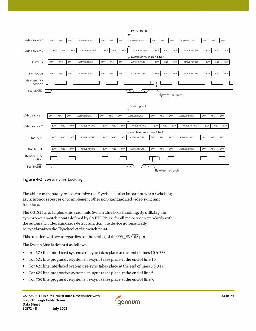
Figure 4-2: Switch Line Locking
The ability to manually re-synchronize the Flywheel is also important when switching asynchronous sources or to implement other non-standardized video switching functions.
The GS1559 also implements automatic Switch Line Lock handling. By utilizing the synchronous switch points defined by SMPTE RP168 for all major video standards with the automatic video standards detect function, the device automatically re-synchronizes the Flywheel at the switch point.
This function will occur regardless of the setting of the FW_EN/DIS pin.
The Switch Line is defined as follows:
• For 525 line interlaced systems: re-sync takes place at the end of lines 10 & 273.
• For 525 line progressive systems: re-sync takes place at the end of line 10.
• For 625 line interlaced systems: re-sync takes place at the end of lines 6 & 319.
• For 625 line progressive systems: re-sync takes place at the end of line 6.
• For 750 line progressive systems: re-sync takes place at the end of line 7.
EAV ANC ACTIVE PICTURE EAV ANCSAV EAV ANC ACTIVE PICTURESAV EAV ANC
ACTIVE PICTURE
SAV
EAV ANC SAV
Video source 1
EAV ANC ACTIVE PICTURE EAV ANCSAV EAV ANC ACTIVE PICTURESAV EAV ANC SAV
ACTIVE PICTURE EAV ANC SAV
Video source 2
EAV ANC ACTIVE PICTURESAV EAV ANC SAVDATA IN ACTIVE PICTURE EAV ANC SAVANCACTIVE PICTURE EAV ANC SAV
Switch point
Flywheel TRSposition
EAV ANC ACTIVE PICTURESAV EAV ANC SAV ANCACTIVE PICTUREDATA OUT ACTIVE PICTURE EAV ANC SAVEAV ANC SAV
FW_EN/DIS
switch video source 1 to 2
Flywheel re-synch
EAV ANC ACTIVE PICTURE EAV ANCSAV EAV ANC ACTIVE PICTURESAV EAV ANC
ACTIVE PICTURE
SAV
EAV ANC SAV
Video source 1
EAV ANC ACTIVE PICTURE EAV ANCSAV EAV ANC ACTIVE PICTURESAV EAV ANC SAV
ACTIVE PICTURE EAV ANC SAV
Video source 2
EAV ANC ACTIVE PICTURESAV EAV ANC SAVDATA IN ACTIVE PICTURE EAV ANC SAVACTIVE PICTURE EAV ANC SAV
Switch point
Flywheel TRSposition
EAV ANC ACTIVE PICTURESAV EAV ANC SAV ACTIVE PICTUREDATA OUT
switch video source 2 to 1
EAV ANC SAV ACTIVE PICTURE EAV ANC SAV
Flywheel re-synchFW_EN/DIS
GS1559 HD-LINX™ II Multi-Rate Deserializer with Loop-Through Cable DriverData Sheet30572 - 8 July 2008
34 of 71

• For 1125 line interlaced systems: re-sync takes place at the end of lines 7 & 568.
• For 1125 line progressive systems: re-sync takes place at the end of line 7.
A full list of all major video standards and switching lines is shown in Table 4-4.
NOTE 1: The Flywheel timing will define the line count such that the line numbers shown in Table 4-4 may not correspond directly to the digital line counts.
NOTE 2: Unless indicated by SMPTE 352M Payload Identifier Packets, the GS1559 will not distinguish between 50/60 frames PsF and 25/30 frames interlaced for the 1125 line video systems; 24 PsF will be identified.
Table 4-4: Switch Line Position for Digital Systems
System Video Format Sampling Signal Standard
Parallel Interface
Serial Interface
Switch Line No.
HD-SDTI 1920x1080 (PsF) 4:2:2 274M 274M + 348M 292M 7
1920x1080 (2:1) 4:2:2 274M 274M + 348M 292M 7, 569
1280x720 (1:1) 4:2:2 296M 296M + 348M 292M 7
SDTI 720x576/50 (2:1) 4:2:2 BT.656 BT.656 + 305M 259M 6, 319
720x483/59.94 (2:1) 4:2:2 125M 125M + 305M 259M 10, 273
750 1280x720/60 (1:1) 4:2:2 296M 296M 296M 7
1280x720/50 (1:1) 4:2:2 296M 296M 296M 7
1280x720/30 (1:1) 4:2:2 296M 296M 296M 7
1280x720/25 (1:1) 4:2:2 296M 296M 296M 7
1280x720/24 (1:1) 4:2:2 296M 296M 296M 7
1125 1920x1080/30 (PsF) 4:2:2 274M + RP211 274M + RP211 292M 7
1920x1080/25 (PsF) 4:2:2 274M + RP211 274M + RP211 292M 7
1920x1080/24 (PsF) 4:2:2 274M + RP211 274M + RP211 292M 7
1920x1080/60 (2:1) 4:2:2 274M + RP211 274M + RP211 292M 7, 569
1920x1080/50 (2:1) 4:2:2 274M + RP211 274M + RP211 292M 7, 569
525 960x483/59.94 (2:1) 4:2:2 267M 349M 292M 10, 273
960x483/59.94 (2:1) 4:2:2 267M 267M 259M 10, 273
720x483/59.94 (2:1) 4:4:4:4 267M 349M 292M 10, 273
720x483/59.94 (2:1) 4:4:4:4 267M 347M 344M 10, 273
720x483/59.94 (2:1) 4:4:4:4 267M RP174 344M 10, 273
720x483/59.94 (2:1) 4:4:4:4 267M RP175 RP175 10, 273
720x483/59.94 (2:1) 4:2:2 125M 349M 292M 10, 273
720x483/59.94 (2:1) 4:2:2 125M 125M 259M 10, 273
720x483/59.94 (1:1) 4:2:2 293M 349M 292M 10
GS1559 HD-LINX™ II Multi-Rate Deserializer with Loop-Through Cable DriverData Sheet30572 - 8 July 2008
35 of 71

4.7.4 HVF Timing Signal Generation
The GS1559 extracts critical timing parameters from either the received TRS signals (FW_EN/DIS = LOW), or from the internal Flywheel-Timing Generator (FW_EN/DIS = HIGH).
Horizontal blanking period (H), Vertical blanking period (V), and even/odd Field (F) timing are all extracted and presented to the application layer via the H:V:F status output pins.
The H signal timing is configurable via the H_CONFIG bit of the internal IOPROC_DISABLE register as either active line based blanking, or TRS based blanking, (see Error Correction and Insertion on page 53).
Active Line Based Blanking is enabled when the H_CONFIG bit is set LOW. In this mode, the H output is HIGH for the entire horizontal blanking period, including the EAV and SAV TRS words. This is the default H timing used by the device.
When H_CONFIG is set HIGH, TRS based blanking is enabled. In this case, the H output will be HIGH for the entire horizontal blanking period as indicated by the H bit in the received TRS ID words.
The timing of these signals is shown in Figure 4-3.
525 720x483/59.94 (1:1) 4:2:2 293M 347M 344M 10
720x483/59.94 (1:1) 4:2:2 293M 293M 294M 10
720x483/59.94 (1:1) 4:2:0 293M 349M 292M 10
720x483/59.94 (1:1) 4:2:0 293M 293M 294M 10
625 720x576/50 (1:1) 4:2:2 BT.1358 349M 292M 6
720x576/50 (1:1) 4:2:2 BT.1358 347M 344M 6
720x576/50 (1:1) 4:2:2 BT.1358 BT.1358 BT.1362 6
720x576/50 (1:1) 4:2:0 BT.1358 349M 292M 6
720x576/50 (1:1) 4:2:0 BT.1358 BT.1358 BT.1362 6
960x576/50 (2:1) 4:2:2 BT.601 349M 292M 6, 319
960x576/50 (2:1) 4:2:2 BT.601 BT.656 259M 6, 319
720x576/50 (2:1) 4:4:4:4 BT.799 349M 292M 6, 319
720x576/50 (2:1) 4:4:4:4 BT.799 347M 344M 6, 319
720x576/50 (2:1) 4:4:4:4 BT.799 BT.799 344M 6, 319
720x576/50 (2:1) 4:4:4:4 BT.799 BT.799 – 6, 319
720x576/50 (2:1) 4:2:2 BT.601 349M 292M 6, 319
720x576/50 (2:1) 4:2:2 BT.601 125M 259M 6, 319
Table 4-4: Switch Line Position for Digital Systems (Continued)
System Video Format Sampling Signal Standard
Parallel Interface
Serial Interface
Switch Line No.
GS1559 HD-LINX™ II Multi-Rate Deserializer with Loop-Through Cable DriverData Sheet30572 - 8 July 2008
36 of 71

Figure 4-3: H, V, F Timing
H:V:F TIMING - HD 20-BIT OUTPUT MODE
PCLK
LUMA DATA OUT
CHROMA DATA OUT
H
XYZ(eav)0000003FF
XYZ(eav)0000003FF
V
F
XYZ(sav)0000003FF
XYZ(sav)0000003FF
H;V:F TIMING AT SAV - HD 10-BIT OUTPUT MODE
0000003FF3FF XYZ(sav)000000 XYZ
(sav)
PCLK
H
V
F
H:V:F TIMING AT EAV - HD 10-BIT OUTPUT MODE
PCLK
0000003FF3FF XYZ(eav)000000 XYZ
(eav) MULTIPLEXED Y/Cr/Cb DATA OUT
H
V
F
MULTIPLEXED Y/Cr/Cb DATA OUT
H:V:F TIMING - SD 20-BIT OUTPUT MODE
PCLK
CHROMA DATA OUT
LUMA DATA OUT
H
0003FF
XYZ(eav)000
V
F
0003FF
XYZ(SAV)000
H:V:F TIMING - SD 10-BIT OUTPUT MODE
MULTIPLEXED Y/Cr/Cb DATA OUT
PCLK
H
V
F
XYZ(eav)0000003FF XYZ
(sav)0000003FF
H SIGNAL TIMING:
H_CONFIG = LOW
H_CONFIG = HIGH
GS1559 HD-LINX™ II Multi-Rate Deserializer with Loop-Through Cable DriverData Sheet30572 - 8 July 2008
37 of 71

4.8 DVB-ASI FunctionalityThe Lock Detect block may drop out of DVB-ASI mode under the following conditions:
• RESET_TRST is asserted LOW
• CDx is HIGH
• SMPTE_BYPASS is asserted HIGH in Slave mode
• DVB_ASI is asserted LOW in Slave mode
DVB_ASI functionality is only supported in Slave mode. To operate in DVB_ASI mode, the device must be in Slave mode and the application layer must set the SD/HD pin HIGH, in addition to setting SMPTE_BYPASS LOW and DVB_ASI HIGH.
4.8.1 DVB-ASI 8b/10b Decoding and Word Alignment
After serial-to-parallel conversion, the internal 10-bit data bus is fed to the DVB-ASI 8b/10b Decode and Word Alignment block. The function of this block is to word align the data to the K28.5 sync characters, and 8b/10b decode and bit-swap the data to achieve bit alignment with the data outputs.
The extracted 8-bit data will be presented to DOUT[17:10], bypassing all internal SMPTE mode data processing.
NOTE: When operating in DVB-ASI mode, DOUT[9:0] are forced LOW.
4.8.2 Status Signal Outputs
In DVB-ASI mode, the DOUT19 and DOUT18 pins will be configured as DVB-ASI status signals SYNCOUT and WORDERR respectively.
SYNCOUT will be HIGH whenever a K28.5 sync character is present on the output. This output may be used to drive the Write Enable signal of an external FIFO, thus providing a means of removing the K28.5 sync characters from the data stream. Parallel DVB-ASI data may then be clocked out of the FIFO at some rate less than 27MHz. See Figure 4-4.
WORDERR will be high whenever the device has detected a running disparity error or illegal code word.
Figure 4-4: DVB-ASI FIFO Implementation Using The GS1559
8 8
AOUT ~ HOUT
WORDERR
PCLK = 27MHz
SYNCOUT
DDI
CLK_IN
CLK_OUT
FIFO
DDI
READ_CLK<27MHz
FE
FF
TS
WE
WORDERRGS1559
GS1559 HD-LINX™ II Multi-Rate Deserializer with Loop-Through Cable DriverData Sheet30572 - 8 July 2008
38 of 71

4.9 Data Through ModeThe GS1559 may be configured by the application layer to operate as a simple serial-to-parallel converter. In this mode, the device presents data to the output data bus without performing any decoding, descrambling or word-alignment.
Data-Through mode is enabled only when the MASTER/SLAVE, SMPTE_BYPASS, and DVB_ASI input pins are set LOW. Under these conditions, the lock detection algorithm enters PLL Lock mode, (see Lock Detect on page 29), such that the device may reclock data not conforming to SMPTE or DVB-ASI streams. The LOCKED pin will indicate analog lock.
When operating in Master mode, the GS1559 will set the SMPTE_BYPASS signal to logic LOW if presented with a data stream without SMPTE TRS ID words. The LOCKED and data bus outputs will be forced LOW and the serial digital loop-through output will be a buffered version of the input.
4.10 Additional Processing FunctionsThe GS1559 contains an additional Data Processing block which is available in SMPTE mode only, (see SMPTE Functionality on page 31).
4.10.1 FIFO Load Pulse
To aid in the application-specific implementation of auto-phasing and line synchronization functions, the GS1559 will generate a FIFO load pulse to reset line-based FIFO storage.
The FIFO_LD output pin will normally be HIGH but will go LOW for one PCLK period, thereby generating a FIFO write reset signal.
The FIFO load pulse will be generated such that it is co-timed to the SAV XYZ code word presented to the output data bus. This ensures that the next PCLK cycle will correspond to the first active sample of the video line.
Figure 4-5 shows the timing relationship between the FIFO_LD signal and the output video data.
GS1559 HD-LINX™ II Multi-Rate Deserializer with Loop-Through Cable DriverData Sheet30572 - 8 July 2008
39 of 71

Figure 4-5: FIFO_LD Pulse Timing
4.10.2 Ancillary Data Detection and Indication
The GS1559 will detect all types of ancillary data in either the vertical or horizontal blanking spaces, and indicate via the status signal output pins YANC and CANC the position of ancillary data in the output data stream. These status signal outputs are synchronous with PCLK and can be used as clock enables to external logic, or as write enables to an external FIFO or other memory device.
When operating in HD mode, (SD/HD = LOW), the YANC signal will be HIGH whenever ancillary data is detected in the Luma data stream, and the CANC signal will be HIGH whenever ancillary data is detected in the Chroma data stream.
PCLK
LUMA DATA OUT
CHROMA DATA OUT
FIFO_LD
3FF 3FF
3FF
3FF
000 000000000 XYZ(SAV)
000000
000000
XYZ(SAV)
XYZ(SAV)
XYZ(SAV)
MULTIPLEXED Y/Cr/Cb DATA OUT
PCLK
FIFO_LD
FIFO LOAD PULSE - HD 10BIT OUTPUT MODE
FIFO LOAD PULSE - HD 20BIT OUTPUT MODE
3FF
3FF
000
000
000000 XYZ(SAV)
MULTIPLEXED Y/Cr/Cb DATA OUT
PCLK
PCLK
LUMA DATA OUT
CHROMA DATA OUT
FIFO_LD
FIFO_LD
XYZ(SAV)
FIFO LOAD PULSE - SD 10BIT OUTPUT MODE
FIFO LOAD PULSE - SD 20BIT OUTPUT MODE
GS1559 HD-LINX™ II Multi-Rate Deserializer with Loop-Through Cable DriverData Sheet30572 - 8 July 2008
40 of 71
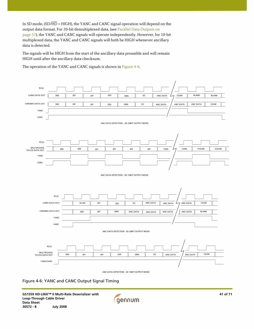
In SD mode, (SD/HD = HIGH), the YANC and CANC signal operation will depend on the output data format. For 20-bit demultiplexed data, (see Parallel Data Outputs on page 57), the YANC and CANC signals will operate independently. However, for 10-bit multiplexed data, the YANC and CANC signals will both be HIGH whenever ancillary data is detected.
The signals will be HIGH from the start of the ancillary data preamble and will remain HIGH until after the ancillary data checksum.
The operation of the YANC and CANC signals is shown in Figure 4-6.
Figure 4-6: YANC and CANC Output Signal Timing
ANC DATA DETECTION - HD 20BIT OUTPUT MODE
ANC DATA DETECTION - HD 10BIT OUTPUT MODE
000
000
000 000
3FF
3FF
3FF
3FF
3FF 3FF3FF 3FF
DID
YDID
DID DBN
DBN
ANC DATA
ANC DATAANC DATA ANC DATA
DC
DC
BLANK BLANKCSUM
CSUM
CANC YCSUM CCSUM
YANC
CANC
PCLK
LUMA DATA OUT
CHROMA DATA OUT
MULTIPLEXED Y/Cr/Cb DATA OUT
YANC
CANC
PCLK
BLANK DID
DBN
ANC DATA
ANC DATA
ANC DATA
ANC DATA
ANC DATA
ANC DATA ANC DATA
ANC DATA
BLANK
CSUM
CSUM3FF
000
000
DID3FF
DBN
DC
3FF
3FF
DC ANC DATA
ANC DATA DETECTION - SD 20BIT OUTPUT MODE
ANC DATA DETECTION - SD 10BIT OUTPUT MODE
PCLK
MULTIPLEXED Y/Cr/Cb DATA OUT
YANC/CANC
PCLK
LUMA DATA OUT
CHROMA DATA OUT
YANC
CANC
GS1559 HD-LINX™ II Multi-Rate Deserializer with Loop-Through Cable DriverData Sheet30572 - 8 July 2008
41 of 71

4.10.2.1 Programmable Ancillary Data Detection
Although the GS1559 will detect all types of ancillary data by default, it also allows the Host Interface to specifically program up to five different ancillary data types for detection. This is accomplished via the ANC_TYPE register (Table 4-5).
For each data type to be detected, the Host Interface must program the DID and/or SDID of the ancillary data type of interest. The GS1559 will compare the received DID and/or SDID with the programmed values and assert YANC and CANC only if an exact match is found.
If any DID or SDID value is set to zero in the ANC_TYPE register, no comparison or match will be made for that value. For example, if the DID is programmed but the SDID is set to zero, the device will detect all ancillary data types matching the DID value, regardless of the SDID.
In the case where all five DID and SDID values are set to zero, the GS1559 will detect all ancillary data types. This is the default setting after device reset.
Where one or more, but less than five, DID and/or SDID values have been programmed, then only those matching ancillary data types will be detected and indicated.
NOTE 1: The GS1559 will always detect EDH ancillary data packets for EDH error detection purposes, regardless of which DID/SDID values have been programmed for ancillary data indication, (see EDH CRC Error Detection on page 50).
NOTE 2: See SMPTE 291M for a definition of ancillary data terms.
Table 4-5: Host Interface Description for Programmable Ancillary Data Type Registers
Register Name Bit Name Description R/W Default
ANC_TYPE1 Address: 005h
15-8 ANC_TYPE1[15:8] Used to program the DID for ancillary data detection at the YANC and CANC output
R/W 0
7-0 ANC_TYPE1[7:0] Used to program the SDID for ancillary data detection at the YANC and CANC output.
Should be set to zero if no SDID is present in the ancillary data packet to be detected.
R/W 0
ANC_TYPE2 Address: 006h
15-8 ANC_TYPE2[15:8] Used to program the DID for ancillary data detection at the YANC and CANC output
R/W 0
7-0 ANC_TYPE2[7:0] Used to program the SDID for ancillary data detection at the YANC and CANC output.
Should be set to zero if no SDID is present in the ancillary data packet to be detected.
R/W 0
ANC_TYPE3 Address: 007h
15-8 ANC_TYPE3[15:8] Used to program the DID for ancillary data detection at the YANC and CANC output
R/W 0
7-0 ANC_TYPE3[7:0] Used to program the SDID for ancillary data detection at the YANC and CANC output.
Should be set to zero if no SDID is present in the ancillary data packet to be detected.
R/W 0
GS1559 HD-LINX™ II Multi-Rate Deserializer with Loop-Through Cable DriverData Sheet30572 - 8 July 2008
42 of 71

4.10.3 SMPTE 352M Payload Identifier
The GS1559 can receive and detect the presence of the SMPTE 352M Payload Identifier Ancillary Data Packet. This four word Payload Identifier Packet may be used to indicate the transport mechanism, frame rate and line scanning/sampling structure.
Upon reception of this packet, the device will extract the four words describing the video format being transported and make this information available to the Host Interface via the four VIDEO_FORMAT_OUT registers (Table 4-6).
The VIDEO_FORMAT_OUT registers will only be updated if the received checksum is the same as the locally calculated checksum.
These registers will be cleared to zero, indicating an undefined format, if the device loses lock to the input data stream (LOCKED = LOW), or if the SMPTE_BYPASS pin is asserted LOW. This is also the default setting after device reset.
The SMPTE 352M packet should be received once per field for interlaced systems and once per frame for progressive systems. If the packet is not received for two complete video frames, the VIDEO_FORMAT_OUT registers will be cleared to zero.
ANC_TYPE4 Address: 008h
15-8 ANC_TYPE4[15:8] Used to program the DID for ancillary data detection at the YANC and CANC output
R/W 0
7-0 ANC_TYPE4[7:0] Used to program the SDID for ancillary data detection at the YANC and CANC output.
Should be set to zero if no SDID is present in the ancillary data packet to be detected.
R/W 0
ANC_TYPE5 Address: 009h
15-8 ANC_TYPE5[15:8] Used to program the DID for ancillary data detection at the YANC and CANC output
R/W 0
7-0 ANC_TYPE5[7:0] Used to program the SDID for ancillary data detection at the YANC and CANC output.
Should be set to zero if no SDID is present in the ancillary data packet to be detected.
R/W 0
Table 4-5: Host Interface Description for Programmable Ancillary Data Type Registers (Continued)
Register Name Bit Name Description R/W Default
GS1559 HD-LINX™ II Multi-Rate Deserializer with Loop-Through Cable DriverData Sheet30572 - 8 July 2008
43 of 71

4.10.4 Automatic Video Standard and Data Format Detection
The GS1559 can independently detect the input video standard and data format by using the timing parameters extracted from the received TRS ID words. This information is presented to the Host Interface via the VIDEO_STANDARD register (Table 4-7).
Total samples per line, active samples per line, total lines per field/frame and active lines per field/frame are also calculated and presented to the Host Interface via the RASTER_STRUCTURE registers (Table 4-8). These line and sample count registers are updated once per frame at the end of line 12. This is in addition to the information contained in the VIDEO_STANDARD register.
After device reset, the four RASTER_STRUCTURE registers default to zero.
4.10.4.1 Video Standard Indication
The video standard codes reported in the VD_STD[4:0] bits of the VIDEO_STANDARD register represent the SMPTE standards as shown in Table 4-9.
In addition to the 5-bit video standard code word, the VIDEO_STANDARD register also contains two status bits. The STD_LOCK bit will be set HIGH whenever the Flywheel has achieved full synchronization. The INT_PROG bit will be set LOW if the detected video standard is progressive and HIGH if the detected video standard is interlaced.
The VD_STD[4:0], STD_LOCK and INT_PROG bits of the VIDEO_STANDARD register will default to zero after device reset. The VD_STD[4:0] and INT_PROG bits will also default to zero if the device loses lock to the input data stream, (LOCKED = LOW), or if the SMPTE_BYPASS pin is asserted LOW. The STD_LOCK bit will retain its previous value if the input is removed.
Table 4-6: Host Interface Description for SMPTE 352M Payload Identifier Registers
Register Name Bit Name Description R/W Default
VIDEO_FORMAT_OUT_B Address: 00Dh
15-8 SMPTE352M Byte 4
Data will be available in this register when Video Payload Identification Packets are detected in the data stream.
R 0
7-0 SMPTE352M Byte 3
Data will be available in this register when Video Payload Identification Packets are detected in the data stream.
R 0
VIDEO_FORMAT_OUT_A Address: 00Ch
15-8 SMPTE352M Byte 2
Data will be available in this register when Video Payload Identification Packets are detected in the data stream.
R 0
7-0 SMPTE352M Byte 1
Data will be available in this register when Video Payload Identification Packets are detected in the data stream.
R 0
GS1559 HD-LINX™ II Multi-Rate Deserializer with Loop-Through Cable DriverData Sheet30572 - 8 July 2008
44 of 71

Table 4-7: Host Interface Description for Video Standard and Data Format Register
Register Name Bit Name Description R/W Default
VIDEO_STANDARD Address: 004h
15 – Not Used. – –
14-10 VD_STD[4:0] Video Data Standard (see Table 4-9). R 0
9 INT_PROG Interlace/Progressive: Set LOW if detected video standard is PROGRESSIVE and is set HIGH if it is INTERLACED.
R 0
8 STD_LOCK Standard Lock: Set HIGH when the Flywheel has achieved full synchronization.
R 0
7-4 CDATA_FORMAT[3:0] Chroma Data Format. Set HIGH in SD mode. Indicates Chroma data format in HD mode (see Table 4-10).
R Fh
3-0 YDATA_FORMAT[3:0] Luma Data Format. Indicates Luma data format in HD mode and data format in SD mode (see Table 4-10).
R Fh
Table 4-8: Host Interface Description for Raster Structure Registers
Register Name Bit Name Description R/W Default
RASTER_STRUCTURE1 Address: 00Eh
15-12 – Not Used. – –
11-0 RASTER_STRUCTURE1[11:0] Words Per Active Line. R 0
RASTER_STRUCTURE2 Address: 00Fh
15-13 – Not Used. – –
12-0 RASTER_STRUCTURE2[12:0] Words Per Total Line. R 0
RASTER_STRUCTURE3 Address: 010h
15-11 – Not Used. – –
10-0 RASTER_STRUCTURE3[10:0] Total Lines Per Frame. R 0
RASTER_STRUCTURE4 Address: 011h
15-11 – Not Used. – –
10-0 RASTER_STRUCTURE4[10:0] Active Lines Per Field. R 0
Table 4-9: Supported Video Standards
VD_STD[4:0] SMPTE Standard
Video Format Length of HANC
Length of Active Video
Total Samples
SMPTE352M Lines
00h 296M (HD) 1280x720/60 (1:1) 358 1280 1650 10
01h 296M (HD) 1280x720/60 (1:1) - EM 198 1440 1650 10
02h 296M (HD) 1280x720/30 (1:1) 2008 1280 3300 10
03h 296M (HD) 1280x720/30 (1:1) - EM 408 2880 3300 10
04h 296M (HD) 1280x720/50 (1:1) 688 1280 1980 10
05h 296M (HD) 1280x720/50 (1:1) - EM 240 1728 1980 10
06h 296M (HD) 1280x720/25 (1:1) 2668 1280 3960 10
07h 296M (HD) 1280x720/25 (1:1) - EM 492 3456 3960 10
GS1559 HD-LINX™ II Multi-Rate Deserializer with Loop-Through Cable DriverData Sheet30572 - 8 July 2008
45 of 71

08h 296M (HD) 1280x720/24 (1:1) 2833 1280 4125 10
09h 296M (HD) 1280x720/24 (1:1) - EM 513 3600 4125 10
0Ah 274M (HD) 1920x1080/60 (2:1) or 1920x1080/30 (PsF)
268 1920 2200 10, 572
0Bh 274M (HD) 1920x1080/30 (1:1) 268 1920 2200 18
0Ch 274M (HD) 1920x1080/50 (2:1) or
1920x1080/25 (PsF)
708 1920 2640 10, 572
0Dh 274M (HD) 1920x1080/25 (1:1) 708 1920 2640 18
0Eh 274M (HD) 1920x1080/25 (1:1) - EM 324 2304 2640 18
0Fh 274M (HD) 1920x1080/25 (PsF) - EM 324 2304 2640 10, 572
10h 274M (HD) 1920x1080/24 (1:1) 818 1920 2750 18
11h 274M (HD) 1920x1080/24 (PsF) 818 1920 2750 10, 572
12h 274M (HD) 1920x1080/24 (1:1) - EM 338 2400 2750 18
13h 274M (HD) 1920x1080/24 (PsF) - EM 338 2400 2750 10, 572
14h 295M (HD) 1920x1080/50 (2:1) 444 1920 2376 10, 572
15h 260M (HD) 1920x1035/60 (2:1) 268 1920 2200 10, 572
16h 125M (SD) 1440x487/60 (2:1)
(Or dual link progressive)
268 1440 1716 10, 276
17h 125M (SD) 1440x507/60 (2:1) 268 1440 1716 10, 276
19h 125M (SD) 525-line 487 generic – – 1716 10, 276
1Bh 125M (SD) 525-line 507 generic – – 1716 10, 276
18h ITU-R BT.656 (SD)
1440x576/50 (2:1)
(Or dual link progressive)
280 1440 1728 9, 322
1Ah ITU-R BT.656 (SD)
625-line generic (EM) – – 1728 9, 322
1Dh Unknown HD – – – – –
1Eh Unknown SD – – – – –
1Ch, 1Fh Reserved – – – – –
Table 4-9: Supported Video Standards (Continued)
VD_STD[4:0] SMPTE Standard
Video Format Length of HANC
Length of Active Video
Total Samples
SMPTE352M Lines
GS1559 HD-LINX™ II Multi-Rate Deserializer with Loop-Through Cable DriverData Sheet30572 - 8 July 2008
46 of 71

4.10.4.2 Data Format Indication
The Luma and Chroma data format codes will be reported in the YDATA_FORMAT[3:0] and CDATA_FORMAT[3:0] bits of the VIDEO_STANDARD register when the device is operating in HD mode, (SD/HD = LOW).
In SD or DVB-ASI mode, the data format code will only appear in the YDATA_FORMAT[3:0] bits. The CDATA_FORMAT[3:0] bits will be set to 'Fh'. These codes represent the data formats listed in Table 4-10.
The YDATA_FORMAT[3:0] and CDATA_FORMAT[3:0] bits of the VIDEO_STANDARD register will default to 'Fh' after device reset. These bits will also default to 'Fh' if the device loses lock to the input data stream, (LOCKED = LOW), or if Data-Through mode is enabled, (see Data Through Mode on page 39).
4.10.5 Error Detection and Indication
The GS1559 contains a number of Error Detection functions to enhance operation of the device when operating in SMPTE mode. These functions, (except Lock Error Detection), will not be available in either DVB-ASI or Data-Through operating modes. See DVB-ASI Functionality on page 38 and Data Through Mode on page 39.
The device maintains an Error Status register at address 001h called ERROR_STATUS (Table 4-11). Each type of error has a specific flag or bit in this register which is set HIGH whenever that error is detected.
The ERROR_STATUS register will be cleared at the start of each video field or when read by the Host Interface, which ever condition occurs first.
All bits of the ERROR_STATUS register except the LOCK_ERR bit will also be cleared if a change in the video standard is detected, or under the following conditions:
Table 4-10: Data Format Codes
YDATA_FORMAT[3:0] or CDATA_FORMAT[3:0]
Data Format Applicable Standards
0h SDTI DVCPRO - No ECC SMPTE 321M
1h SDTI DVCPRO - ECC SMPTE 321M
2h SDTI DVCAM SMPTE 322M
3h SDTI CP SMPTE 326M
4h Other SDTI fixed block size –
5h Other SDTI variable block size –
6h SDI –
7h DVB-ASI –
8h TDM data SMPTE 346M
9h ~ Eh Reserved –
Fh Unknown data format –
GS1559 HD-LINX™ II Multi-Rate Deserializer with Loop-Through Cable DriverData Sheet30572 - 8 July 2008
47 of 71

• RESET_TRST is held LOW
• LOCKED is asserted LOW
• SMPTE_BYPASS is asserted LOW in slave mode
In addition to the ERROR_STATUS register, a register called ERROR_MASK (Table 4-12) is included which allows the Host Interface to select the specific error conditions that will be detected. There is one bit in the ERROR_MASK register for each type of error represented in the ERROR_STATUS register.
The bits of the ERROR_MASK register will default to 'zero' after device reset, thus enabling all error types to be detected. The Host Interface may disable individual error detection by setting the corresponding bit HIGH in this register.
Error conditions are also indicated to the application layer via the status signal pin DATA_ERROR. This output pin is a logical 'OR'ing of each error status flag stored in the ERROR_STATUS register. DATA_ERROR is normally HIGH, but will be set LOW by the device when an error condition that has not been masked is detected.
GS1559 HD-LINX™ II Multi-Rate Deserializer with Loop-Through Cable DriverData Sheet30572 - 8 July 2008
48 of 71

Table 4-11: Host Interface Description for Error Status Register
Register Name Bit Name Description R/W Default
ERROR_STATUS Address: 001h
15-11 – Not Used. – –
10 VD_STD_ERR Video Standard Error Flag. Set HIGH when a mismatch between the received SMPTE352M packets and the calculated video standard occurs.
R 0
9 FF_CRC_ERR Full Field CRC Error Flag. Set HIGH in SD mode when a Full Field (FF) CRC mismatch has been detected in Field 1 or 2.
R 0
8 AP_CRC_ERR Active Picture CRC Error Flag. Set HIGH in SD mode when an Active Picture (AP) CRC mismatch has been detected in Field 1 or 2.
R 0
7 LOCK_ERR Lock Error Flag. Set HIGH whenever the LOCK pin is LOW (indicating the device not correctly locked).
R 0
6 CCS_ERR Chroma Checksum Error Flag. Set HIGH when ancillary data packet checksum error has been detected in the C channel.
R 0
5 YCS_ERR Luma Checksum Error Flag. Set HIGH when ancillary data packet checksum error has been detected in the Y channel.
R 0
4 CCRC_ERR Chroma CRC Error Flag. Set HIGH in HD mode when a mismatch occurs between the calculated and received CRC values in the C channel.
R 0
3 YCRC_ERR Luma CRC Error Flag. Set HIGH in HD mode when a mismatch occurs between the calculated and received CRC values in the Y channel.
R 0
2 LNUM_ERR Line Number Error Flag. Set HIGH in HD mode when a mismatch occurs between the calculated and received line numbers.
R 0
1 SAV_ERR Start of Active Video Error Flag. Set HIGH when TRS errors are detected in either 8-bit or 10-bit TRS words. In HD mode only Y channel TRS codes will be checked. FW_EN/DIS must be set HIGH.
R 0
0 EAV_ERR End of Active Video Error Flag. Set HIGH when TRS errors are detected in either 8-bit or 10-bit TRS words. In HD mode only Y channel TRS codes will be checked. FW_EN/DIS must be set HIGH.
R 0
GS1559 HD-LINX™ II Multi-Rate Deserializer with Loop-Through Cable DriverData Sheet30572 - 8 July 2008
49 of 71

4.10.5.1 Video Standard Error Detection
If a mismatch between the received SMPTE 352M packets and the calculated video standard occurs, the GS1559 will indicate a video standard error by setting the VD_STD_ERR bit of the ERROR_STATUS register HIGH.
4.10.5.2 EDH CRC Error Detection
The GS1559 calculates Full Field (FF) and Active Picture (AP) CRC words according to SMPTE RP165 in support of Error Detection and Handling packets in SD signals.
These calculated CRC values are compared with the received CRC values. If a mismatch is detected, the error is flagged in the AP_CRC_ERR and/or FF_CRC_ERR bits of the ERROR_STATUS register. These two flags are shared between fields 1 and 2.
The AP_CRC_ERR bit will be set HIGH when an active picture CRC mismatch has been detected in field 1 or 2. The FF_CRC_ERR bit will be set HIGH when a full field CRC mismatch has been detected in field 1 or 2.
EDH CRC errors will only be indicated when the device is operating in SD mode (SD/HD = HIGH), and when the device has correctly received EDH packets.
SMPTE RP165 specifies the calculation ranges and scope of EDH data for standard 525 and 625 component digital interfaces. The GS1559 will utilize these standard ranges by default.
If the received video format does not correspond to 525 or 625 digital component video standards as determined by the Flywheel pixel and line counters, then one of two schemes for determining the EDH calculation ranges will be employed:
Table 4-12: Host Interface Description for Error Mask Register
Register Name Bit Name Description R/W Default
ERROR_MASK Address: 01Ah
15-11 – Not Used. – –
10 VD_STD_ERR_MASK Video Standard Error Flag Mask bit. R/W 0
9 FF_CRC_ERR_MASK Full Field CRC Error Flag Mask bit. R/W 0
8 AP_CRC_ERR_MASK Active Picture CRC Error Flag Mask bit. R/W 0
7 LOCK_ERR_MASK Lock Error Flag Mask bit. R/W 0
6 CCS_ERR_MASK Chroma Checksum Error Flag Mask bit. R/W 0
5 YCS_ERR_MASK Luma Checksum Error Flag Mask bit. R/W 0
4 CCRC_ERR_MASK Chroma CRC Error Flag Mask bit. R/W 0
3 YCRC_ERR_MASK Luma CRC Error Flag Mask bit. R/W 0
2 LNUM_ERR_MASK Line Number Error Flag Mask bit. R/W 0
1 SAV_ERR_MASK Start of Active Video Error Flag Mask bit. R/W 0
0 EAV_ERR_MASK End of Active Video Error Flag Mask bit. R/W 0
GS1559 HD-LINX™ II Multi-Rate Deserializer with Loop-Through Cable DriverData Sheet30572 - 8 July 2008
50 of 71

1. Ranges will be based on the line and pixel ranges programmed by the Host Interface; or
2. In the absence of user-programmed calculation ranges, ranges will be determined from the received TRS timing information.
The registers available to the Host Interface for programming EDH calculation ranges include Active Picture and Full Field line start and end positions for both fields. Table 4-13 shows the relevant registers, which default to 'zero' after device reset.
If any or all of these register values are zero, then the EDH CRC calculation ranges will be determined from the Flywheel generated H signal. The first active and full field pixel will always be the first pixel after the SAV TRS code word. The Last Active and Full Field pixel will always be the last pixel before the start of the EAV TRS code words.
Table 4-13: Host Interface Description for EDH Calculation Range Registers
Register Name Bit Name Description R/W Default
AP_LINE_START_F0 Address: 012h
15-10 – Not Used. – –
9-0 AP_LINE_START_F0[9:0] Field 0 Active Picture start line data used to set EDH calculation range outside of SMPTE RP 165 values.
R/W 0
AP_LINE_END_F0 Address: 013h
15-10 – Not Used. – –
9-0 AP_LINE_END_F0[9:0] Field 0 Active Picture end line data used to set EDH calculation range outside of SMPTE RP 165 values.
R/W 0
AP_LINE_START_F1 Address: 014h
15-10 – Not Used. – –
9-0 AP_LINE_START_F1[9:0] Field 1 Active Picture end line data used to set EDH calculation range outside of SMPTE RP 165 values.
R/W 0
AP_LINE_END_F1 Address: 015h
15-10 – Not Used. – –
9-0 AP_LINE_END_F1[9:0] Field 1 Active Picture end line data used to set EDH calculation range outside of SMPTE RP 165 values.
R/W 0
GS1559 HD-LINX™ II Multi-Rate Deserializer with Loop-Through Cable DriverData Sheet30572 - 8 July 2008
51 of 71

4.10.5.3 Lock Error Detection
The LOCKED pin of the GS1559 indicates the lock status of the Reclocker and Lock Detect blocks of the device. Only when the LOCKED pin is asserted HIGH has the device correctly locked to the received data stream, (see Lock Detect on page 29).
The GS1559 will also indicate Lock Error to the Host Interface when LOCKED = LOW by setting the LOCK_ERR bit in the ERROR_STATUS register HIGH.
4.10.5.4 Ancillary Data Checksum Error Detection
The GS1559 will calculate checksums for all received ancillary data and compare the calculated values to the received checksum words. If a mismatch is detected, the error is flagged in the CCS_ERR and/or YCS_ERR bits of the ERROR_STATUS register.
When operating in HD mode, (SD/HD = LOW), the device will make comparisons on both the Y and C channels separately. If an error condition in the Y channel is detected, the YCS_ERR bit will be set HIGH. If an error condition in the C channel is detected, the CCS_ERR bit will be set HIGH.
When operating in SD mode, (SD/HD = HIGH), only the YCS_ERR bit will be set HIGH when checksum errors are detected.
Although the GS1559 will calculate and compare checksum values for all ancillary data types by default, the Host Interface may program the device to check only certain types of ancillary data checksums.
This is accomplished via the ANC_TYPE register as described in Programmable Ancillary Data Detection on page 42.
FF_LINE_START_F0 Address: 016h
15-10 – Not Used. – –
9-0 FF_LINE_START_F0[9:0] Field 0 Full Field start line data used to set EDH calculation range outside of SMPTE RP 165 values.
R/W 0
FF_LINE_END_F0 Address: 017h
15-10 – Not Used. – –
9-0 FF_LINE_END_F0[9:0] Field 0 Full Field start line data used to set EDH calculation range outside of SMPTE RP 165 values.
R/W 0
FF_LINE_START_F1 Address: 018h
15-10 – Not Used. – –
9-0 FF_LINE_START_F1[9:0] Field 1 Full Field start line data used to set EDH calculation range outside of SMPTE RP 165 values.
R/W 0
FF_LINE_END_F1 Address: 019h
15-10 – Not Used. – –
9-0 FF_LINE_END_F1[9:0] Field 1 Full Field end line data used to set EDH calculation range outside of SMPTE RP 165 values.
R/W 0
Table 4-13: Host Interface Description for EDH Calculation Range Registers (Continued)
Register Name Bit Name Description R/W Default
GS1559 HD-LINX™ II Multi-Rate Deserializer with Loop-Through Cable DriverData Sheet30572 - 8 July 2008
52 of 71
4.10.5.5 Line Based CRC Error Detection
The GS1559 will calculate line based CRC words for HD video signals for both the Y and C data channels. These calculated CRC values are compared with the received CRC values and any mismatch is flagged in the YCRC_ERR and/or CCRC_ERR bits of the ERROR_STATUS register.
Line based CRC error flags will only be generated when the device is operating in HD mode, (SD/HD = LOW).
If a CRC error is detected in the Y channel, the YCRC_ERR bit in the Error Status Register will be set HIGH. If a CRC error is detected in the C channel, the CCRC_ERR bit in the Error Status Register is set HIGH. Y and C CRC errors will also be generated if CRC values are not received.
4.10.5.6 HD Line Number Error Detection
When operating in HD mode, the GS1559 will calculate line numbers based on the timing generated by the internal Flywheel. These calculated line numbers are compared with the received line numbers for the Y channel data and any mismatch is flagged in the LNUM_ERR bit of the ERROR_STATUS.
Line Number Errors will also be generated if line number values are not received.
4.10.5.7 TRS Error Detection
TRS Errors Flags are generated by the GS1559 when:
1. The received TRS timing does not correspond to the internal Flywheel timing; or
2. The received TRS hamming codes are incorrect.
Both 8-bit and 10-bit SAV and EAV TRS words are checked for timing and data integrity errors. These are flagged via the SAV_ERR and/or EAV_ERR bits of the ERROR_STATUS register.
Timing-based TRS errors will only be generated if the FW_EN/DIS pin is set HIGH.
NOTE: In HD mode, (SD/HD = LOW), only the Y channel TRS codes will be checked for errors.
4.10.6 Error Correction and Insertion
In addition to Signal Error Detection and Indication, the GS1559 may also correct certain types of errors by inserting corrected code words, checksums and CRC values into the data stream. These features are only available in SMPTE mode and IOPROC_EN/DIS must be set HIGH. Individual correction features may be enabled or disabled via the IOPROC_DISABLE register (Table 4-14).
All of the IOPROC_DISABLE register bits default to 'zero' after device reset, enabling all of the processing features. To disable any individual error correction feature, the Host Interface must set the corresponding bit HIGH in the IOPROC_DISABLE register.
GS1559 HD-LINX™ II Multi-Rate Deserializer with Loop-Through Cable DriverData Sheet30572 - 8 July 2008
53 of 71

4.10.6.1 Illegal Code Remapping
If the ILLEGAL_REMAP bit of the IOPROC_DISABLE register is set LOW, the GS1559 will remap all codes within the Active Picture between the values of 3FCh and 3FFh to 3FBh. All codes within the Active Picture area between the values of 000h and 003h will be re-mapped to 004h.
In addition, 8-bit TRS and ancillary data preambles will be remapped to 10-bit values if this feature is enabled.
4.10.6.2 EDH CRC Error Correction
The GS1559 will generate and insert Active Picture and Full Field CRC words into the EDH data packets received by the device. This feature is only available in SD mode and is enabled by setting the EDH_CRC_INS bit of the IOPROC_DISABLE register LOW.
EDH CRC calculation ranges are described in EDH CRC Error Detection on page 50.
NOTE: Although the GS1559 will modify and insert EDH CRC words and EDH packet checksums, EDH error flags will not be updated by the device.
Table 4-14: Host Interface Description for Internal Processing Disable Register
Register Name Bit Name Description R/W Default
IOPROC_DISABLE Address: 000h
15-9 – Not Used. – –
8 H_CONFIG Horizontal sync timing output configuration. Set LOW for active line blanking timing. Set HIGH for H blanking based on the H bit setting of the TRS words. See Figure 4-2.
0
7-6 – Not Used. – –
5 ILLEGAL_REMAP Illegal Code re-mapping. Correction of illegal code words within the active picture. Set HIGH to disable. The IOPROC_EN/DIS pin must be set HIGH.
R/W 0
4 EDH_CRC_INS Error Detection & Handling (EDH) Cyclical Redundancy Check (CRC) error correction insertion. In SD mode set HIGH to disable. The IOPROC_EN/DIS pin must be set HIGH.
R/W 0
3 ANC_CSUM_INS Ancillary Data Check-sum insertion. Set HIGH to disable. The IOPROC_EN/DIS pin must be set HIGH.
R/W 0
2 CRC_INS Y and C line based CRC insertion. In HD mode, inserts line based CRC words in both the Y and C channels. Set HIGH to disable. The IOPROC_EN/DIS pin must be set HIGH.
R/W 0
1 LNUM_INS Y and C line number insertion. In HD mode set HIGH to disable. The IOPROC_EN/DIS pin must be set HIGH.
R/W 0
0 TRS_INS Timing Reference Signal Insertion. Set HIGH to disable. The IOPROC_EN/DIS pin must be set HIGH.
R/W 0
GS1559 HD-LINX™ II Multi-Rate Deserializer with Loop-Through Cable DriverData Sheet30572 - 8 July 2008
54 of 71

4.10.6.3 Ancillary Data Checksum Error Correction
When ancillary Data Checksum Error Correction and Insertion is enabled, the GS1559 will generate and insert ancillary data checksums for all ancillary data words by default. Where user specified ancillary data has been programmed into the device (Programmable Ancillary Data Detection on page 42), only the checksums for the programmed ancillary data types will be corrected.
This feature is enabled when the ANC_CSUM_INS bit of the IOPROC_DISABLE register is set LOW.
4.10.6.4 Line Based CRC Correction
The GS1559 will generate and insert line based CRC words into both the Y and C channels of the data stream. This feature is only available in HD mode and is enabled by setting the CRC_INS bit of the IOPROC_DISABLE register LOW.
4.10.6.5 HD Line Number Error Correction
In HD mode, the GS1559 will calculate and insert line numbers into the Y and C channels of the output data stream.
Line Number Generation is in accordance with the relevant HD video standard as determined by the device, (see Automatic Video Standard and Data Format Detection on page 44).
This feature is enabled when SD/HD = LOW, and the LNUM_INS bit of the IOPROC_DISABLE register is set LOW.
4.10.6.6 TRS Error Correction
When TRS error correction and insertion is enabled, the GS1559 will generate and insert 10-bit TRS code words as required.
TRS Word Generation will be performed in accordance with the timing parameters generated by the Flywheel to provide an element of noise immunity. As a result, TRS correction will only take place if the Flywheel is enabled, (FW_EN/DIS = HIGH).
In addition, the TRS_INS bit of the IOPROC_DISABLE register must be set LOW.
4.10.7 EDH Flag Detection
As described in EDH CRC Error Detection on page 50, the GS1559 can detect EDH packets in the received data stream. The EDH flags for Ancillary Data, Active Picture and Full Field areas are extracted from the detected EDH packets and placed in the EDH_FLAG register of the device (Table 4-15).
One set of flags is provided for both fields 1 and 2. Field 1 flag data will be overwritten by field 2 flag data.
The EDH_FLAG register may be read by the Host Interface at any time during the received frame except on the lines defined in SMPTE RP165 where these flags are updated.
GS1559 HD-LINX™ II Multi-Rate Deserializer with Loop-Through Cable DriverData Sheet30572 - 8 July 2008
55 of 71

NOTE 1: By programming the ANC_TYPE1 register (005h) with the DID word for EDH ancillary packets, the application layer may detect a high-to-low transition on either the YANC or CANC output pin of the GS1559 to determine (a) when EDH packets have been received by the device, and (b) when the EDH_FLAG register can be read by the Host Interface. See Ancillary Data Detection and Indication on page 40 for more information on ancillary data detection and indication.
NOTE 2: The bits of the EDH_FLAG register are sticky and will not be cleared by a read operation. If the GS1559 is decoding a source containing EDH packets, where EDH flags may be set, and the source is replaced by one without EDH packets, the EDH_FLAG register will not be cleared.
NOTE 3: The GS1559 will detect EDH flags, but will not update the flags if an EDH CRC error is detected. Gennum's GS1532 Multi-Rate Serializer allows the host to individually set EDH flags.
Table 4-15: Host Interface Description for EDH Flag Register
Register Name Bit Name Description R/W Default
EDH_FLAG Address: 003h
15 – Not used. – –
14 ANC-UES out Ancillary Unknown Error Status flag. R 0
13 ANC-IDA out Ancillary Internal device error Detected Already flag. R 0
12 ANC-IDH out Ancillary Internal device error Detected Here flag. R 0
11 ANC-EDA out Ancillary Error Detected Already flag. R 0
10 ANC-EDH out Ancillary Error Detected Here flag. R 0
9 FF-UES out Full Field Unknown Error Status flag. R 0
8 FF-IDA out Full Field Internal device error Detected Already flag. R 0
7 FF-IDH out Full Field Internal device error Detected Here flag. R 0
6 FF-EDA out Full Field Error Detected Already flag. R 0
5 FF-EDH out Full Field Error Detected Here flag. R 0
4 AP-UES out Active Picture Unknown Error Status flag. R 0
3 AP-IDA out Active Picture Internal device error Detected Already flag.
R 0
2 AP-IDH out Active Picture Internal device error Detected Here flag. R 0
1 AP-EDA out Active Picture Error Detected Already flag. R 0
0 AP-EDH out Active Picture Error Detected Here flag. R 0
GS1559 HD-LINX™ II Multi-Rate Deserializer with Loop-Through Cable DriverData Sheet30572 - 8 July 2008
56 of 71

4.11 Parallel Data OutputsData outputs leave the device on the rising edge of PCLK as shown in Figure 4-7 and Figure 4-8.
The data may be scrambled or unscrambled, framed or unframed, and may be presented in 10-bit or 20-bit format. The output data bus width is controlled independently from the internal data bus width by the 20bit/10bit input pin.
Likewise, the output data format is defined by the setting of the external SD/HD, SMPTE_BYPASS and DVB_ASI pins. Recall that in Slave mode, these pins are set by the application layer as inputs to the device. In Master mode, however, the GS1559 sets the SD/HD and SMPTE_BYPASS pins as output status signals.
4.11.1 Parallel Data Bus Buffers
The parallel data outputs of the GS1559 are driven by high-impedance buffers which support both LVTTL and LVCMOS levels. These buffers use a separate power supply of +3.3V DC supplied via the IO_VDD and IO_GND pins.
All output buffers, including the PCLK output, may be driven to a high-impedance state if the RESET_TRST signal is asserted LOW.
Note that the timing characteristics of the parallel data output buffers are optimized for 10-bit HD operation. As shown in Figure 4-7, the output data hold time for HD is 1.5ns.
Due to this optimization, however, the output data hold time for SD data is so small that the rising edge of the PCLK is nearly incident with the data transition. To improve output hold time at SD rates, the PCLK output is inverted is SD mode, (SD/HD = HIGH). This is shown in Figure 4-8.
Figure 4-7: HD PCLK to Data Timing
PCLK
DOUT[19:0] DATA
Control signal output
tOH
tOD
HD MODE
GS1559 HD-LINX™ II Multi-Rate Deserializer with Loop-Through Cable DriverData Sheet30572 - 8 July 2008
57 of 71

Figure 4-8: SD PCLK to Data Timing
4.11.2 Parallel Output in SMPTE Mode
When the device is operating in SMPTE mode, (see SMPTE Functionality on page 31), both SD and HD data may be presented to the output bus in either multiplexed or demultiplexed form depending on the setting of the 20bit/10bit input pin.
In 20-bit mode, (20bit/10bit = HIGH), the output data will be word aligned, demultiplexed Luma and Chroma data. Luma words will always appear on DOUT[19:10] while Chroma words will occupy DOUT[9:0].
In 10-bit mode, (20bit/10bit = LOW), the output data will be word aligned, multiplexed Luma and Chroma data. The data will be presented on DOUT[19:10], and the device will force DOUT[9:0] LOW.
4.11.3 Parallel Output in DVB-ASI Mode
When operating in DVB-ASI mode, (see DVB-ASI Functionality on page 38), the GS1559 automatically configures the output port for 10-bit operation regardless of the setting of the 20bit/10bit pin.
The extracted 8-bit data words will be presented on DOUT[17:10] such that DOUT17 = HOUT is the most significant bit of the decoded transport stream data and DOUT10 = AOUT is the least significant bit.
In addition, DOUT19 and DOUT18 will be configured as the DVB-ASI status signals SYNCOUT and WORDERR respectively. See Status Signal Outputs on page 38 for a description of these DVB-ASI specific output signals.
DOUT[9:0] will be forced LOW when the GS1559 is operating in DVB-ASI mode.
PCLK
DOUT[19:0] DATA
Control signal output
tOH
tOD
SD MODE
GS1559 HD-LINX™ II Multi-Rate Deserializer with Loop-Through Cable DriverData Sheet30572 - 8 July 2008
58 of 71

4.11.4 Parallel Output in Data-Through Mode
When operating in Data-Through mode, (see Data Through Mode on page 39), the GS1559 presents data to the output data bus without performing any decoding, descrambling or word-alignment.
As described in Data Through Mode on page 39, the data bus outputs will be forced to logic LOW if the device is set to operate in Master mode but cannot identify SMPTE TRS ID in the input data stream.
4.11.5 Parallel Output Clock (PCLK)
The frequency of the PCLK output signal of the GS1559 is determined by the output data format. Table 4-16 below lists the possible output signal formats and their corresponding parallel clock rates. Note that DVB-ASI output will always be in 10-bit format, regardless of the setting of the 20bit/10bit pin.
Table 4-16: Parallel Data Output Format
Output Data Format DOUT [19:10]
DOUT [9:0]
PCLK Status / Control Signals*
20bit/ 10bit
SD/HD SMPTE_BYPASS DVB_ASI
SMPTE MODE
20bit DEMULTIPLEXED SD LUMA CHROMA 13.5MHz HIGH HIGH HIGH LOW
10bit MULTIPLEXED SD LUMA / CHROMA
FORCED LOW
27MHz LOW HIGH HIGH LOW
20bit DEMULTIPLEXED HD LUMA CHROMA 74.25 or 74.25/ 1.001MHz
HIGH LOW HIGH LOW
10bit MULTIPLEXED HD LUMA / CHROMA
FORCED LOW
148.5 or 148.5/ 1.001MHz
LOW LOW HIGH LOW
DVB-ASI MODE
10bit DVB-ASI DVB-ASI DATA
FORCED LOW
27MHz HIGH HIGH LOW HIGH
DVB-ASI DATA
FORCED LOW
27MHz LOW HIGH LOW HIGH
GS1559 HD-LINX™ II Multi-Rate Deserializer with Loop-Through Cable DriverData Sheet30572 - 8 July 2008
59 of 71

4.12 GSPI Host InterfaceThe GSPI, or Gennum Serial Peripheral Interface, is a 4-wire interface provided to allow the host to enable additional features of the device and/or to provide additional status information through configuration registers in the GS1559.
The GSPI comprises a Serial Data Input signal SDIN, Serial Data Output signal SDOUT, an active low Chip Select CS, and a Burst Clock SCLK. The Burst Clock must have a duty cycle between 40% and 60%.
Because these pins are shared with the JTAG interface port, an additional control signal pin JTAG/HOST is provided. When JTAG/HOST is LOW, the GSPI interface is enabled.
When operating in GSPI mode, the SCLK, SDIN, and CS signals are provided by the Host Interface. The SDOUT pin is a high-impedance output allowing multiple devices to be connected in parallel and selected via the CS input. The interface is illustrated in Figure 4-9.
All read or write access to the GS1559 is initiated and terminated by the Host Processor. Each access always begins with a 16-bit Command Word on SDIN indicating the address of the register of interest. This is followed by a 16-bit Data Word on SDIN in Write mode, or a 16-bit Data Word on SDOUT in Read mode.
Figure 4-9: Gennum Serial Peripheral Interface (GSPI)
DATA-THROUGH MODE**
20bit DEMULTIPLEXED SD DATA DATA 13.5MHz HIGH HIGH LOW LOW
10bit MULTIPLEXED SD DATA FORCED LOW
27MHz LOW HIGH LOW LOW
20bit DEMULTIPLEXED HD DATA DATA 74.25 or 74.25/ 1.001MHz
HIGH LOW LOW LOW
10bit MULTIPLEXED HD DATA FORCED LOW
148.5 or 148.5/ 1.001MHz
LOW LOW LOW LOW
*NOTE1: Recall that SD/HD, SMPTE_BYPASS, and DVB_ASI are input control pins in slave mode to be set by the application layer, but the SD/HD and SMPTE_BYPASS pinsare output status signals set by the device in Master mode.
**NOTE 2: Data-Through mode is only available in Slave mode Data Through Mode on page 39.
Table 4-16: Parallel Data Output Format (Continued)
SCLK
CS
SDOUT
SDIN
SCLK
CS
SDIN
SDOUT
Application Host GS1559
GS1559 HD-LINX™ II Multi-Rate Deserializer with Loop-Through Cable DriverData Sheet30572 - 8 July 2008
60 of 71

4.12.1 Command Word Description
The Command Word is transmitted MSB first and contains a Read/Write bit, nine reserved bits and a 6-bit register address. Set R/W = '1' to read and R/W = '0' to write from the GSPI.
Command Words are clocked into the GS1559 on the rising edge of the Serial Clock SCLK. The appropriate Chip Select, CS, signal must be asserted low a minimum of 1.5ns (t0 in Figure 4-12 and Figure 4-13) before the first clock edge to ensure proper operation.
Each Command Word must be followed by only one Data Word to ensure proper operation.
Figure 4-10: Command Word
Figure 4-11: Data Word
4.12.2 Data Read and Write Timing
Read and Write mode timing for the GSPI interface is shown in Figure 4-12 and Figure 4-13 respectively. The maximum SCLK frequency allowed is 6.6MHz.
When writing to the registers via the GSPI, the MSB of the Data Word may be presented to SDIN immediately following the falling edge of the LSB of the Command Word. All SDIN data is sampled on the rising edge of SCLK.
When reading from the registers via the GSPI, the MSB of the Data word will be available on SDOUT 12ns following the falling edge of the LSB of the Command word, and thus may be read by the Host on the very next rising edge of the clock. The remaining bits are clocked out by the GS1559 on the negative edges of SCLK.
Figure 4-12: GSPI Read Mode Timing
R/W RSV RSV RSV A0A1A2A3A4A5RSVRSVRSVRSVRSV RSV
MSB LSB
D15 D14 D13 D12 D0D1D2D3D4D5D6D7D8D9D11 D10
MSB LSB
SDOUT
R/W RSV RSV A0A1A2A3A4A5RSVRSVRSVRSVRSVRSV
D15 D14 D13 D12 D0D1D2D3D4D5D6D7D8D9D11 D10
SCLK
CS
SDIN RSV
t0 t2
t3input data setup time
dutycycle t4 period t5
t6output datahold time
GS1559 HD-LINX™ II Multi-Rate Deserializer with Loop-Through Cable DriverData Sheet30572 - 8 July 2008
61 of 71

Figure 4-13: GSPI Write Mode Timing
4.12.3 Configuration and Status Registers
Table 4-17 summarizes the GS1559's internal status and configuration registers.
All of these registers are available to the Host via the GSPI and are all individually addressable.
Where status registers contain less than the full 16 bits of information however, two or more registers may be combined at a single logical address.
R/W RSV RSV A0A1A2A3A4A5RSVRSVRSVRSVRSVRSV D15 D14 D13 D12 D0D1D2D3D4D5D6D7D8D9D11 D10
SCLK
CS
SDIN RSV
t0 t2
t3input data setup time
dutycycle t4 period
Table 4-17: GS1559 internal registers
Address Register Name See Section
000h IOPROC_DISABLE Section 4.10.6
001h ERROR_STATUS Section 4.10.5
003h EDH_FLAG Section 4.10.7
004h VIDEO_STANDARD Section 4.10.4
005h - 009h ANC_TYPE Section 4.10.2.1
00Ch - 00Dh VIDEO_FORMAT Section 4.10.3
00Eh - 011h RASTER_STRUCTURE Section 4.10.4
012h - 019h EDH_CALC_RANGES Section 4.10.5.2
01Ah ERROR_MASK Section 4.10.5
GS1559 HD-LINX™ II Multi-Rate Deserializer with Loop-Through Cable DriverData Sheet30572 - 8 July 2008
62 of 71

4.13 JTAGWhen the JTAG/HOST input pin of the GS1559 is set HIGH, the Host Interface port will be configured for JTAG test operation. In this mode, pins H4 to H6 and J6 become TMS, TCK, TDO, and TDI. In addition, the RESET_TRST pin will operate as the test reset pin.
Boundary scan testing using the JTAG interface will be enabled in this mode.
There are two methods in which JTAG can be used on the GS1559:
1. As a stand-alone JTAG interface to be used at in-circuit ATE (Automatic Test Equipment) during PCB assembly; or
2. Under control of the host for applications such as system power on self tests.
When the JTAG tests are applied by ATE, care must be taken to disable any other devices driving the digital I/O pins. If the tests are to be applied only at ATE, this can be accomplished with tri-state buffers used in conjunction with the JTAG/HOST input signal. This is shown in Figure 4-14.
Figure 4-14: In-Circuit JTAG
Alternatively, if the test capabilities are to be used in the system, the Host may still control the JTAG/HOST input signal, but some means for tri-stating the Host must exist in order to use the interface at ATE. This is represented in Figure 4-15.
Figure 4-15: System JTAG
Please contact your Gennum representative to obtain the BSDL model for the GS1559.
Application HOST GS1559
CS_TMS
SCLK_TCK
SDIN_TDI
SDOUT_TDO
JTAG_HOST
In-circuit ATE probe
Application HOST GS1559
CS_TMS
SCLK_TCK
SDIN_TDI
SDOUT_TDO
JTAG_HOSTIn-circuit ATE probe
Tri-State
GS1559 HD-LINX™ II Multi-Rate Deserializer with Loop-Through Cable DriverData Sheet30572 - 8 July 2008
63 of 71

4.14 Device Power UpThe GS1559 has a recommended power supply sequence. To ensure correct power up, power the CORE_VDD pins before the IO_VDD pins.
Device pins may also be driven prior to power up without causing damage.
To ensure that all internal registers are cleared upon power-up, the application layer must hold the RESET_TRST signal LOW for a minimum of 1ms after the core power supply has reached the minimum level specified in DC Electrical Characteristics on page 16. See Figure 4-16.
4.15 Device ResetIn order to initialize all internal operating conditions to their default states the application layer must hold the RESET_TRST signal LOW for a minimum of treset = 1ms.
When held in reset, all device outputs will be driven to a high-impedance state.
Figure 4-16: Reset Pulse
CORE_VDD
RESET_TRSTtreset
+1.65V+1.8V
Reset Reset
treset
GS1559 HD-LINX™ II Multi-Rate Deserializer with Loop-Through Cable DriverData Sheet30572 - 8 July 2008
64 of 71

5. Application Reference Design
5.1 Typical Application Circuit (Part A)
GS1574A
SDI
CD
SDI
VEE_D
MU
TE
VC
C_D
AG
C
BY
PASS
MC
LAD
J
VEE_A
NOTE: All resistors in Ohms, capacitors in Farads, and inductors in Henrys, unless otherwise noted.
VEE_A
AG
C
VC
C_A
SDO
SDO
VEE_D
10n
1
10n
SDO
4u7
4u7
+
+
SDO
CD
MUTE
BYPASS
MCLADJ470n
6.2n
75
SDI
1u
75
1u
37R4
EQ_VCC
4
5 6
2
3
87
16
12
13
11
1415
9
10
470n
EQ_VCC
EQ_GNDEQ_GND
EQ_GND EQ_GND
EQ_GND
EQ_GND
EQ_GND
GS1559 HD-LINX™ II Multi-Rate Deserializer with Loop-Through Cable DriverData Sheet30572 - 8 July 2008
65 of 71

5.2 Typical Application Circuit (Part B)
G S 1 5 5 9
VC
O_G
ND
VC
O_V
CC
A2
A3
VC
OV
COLF
A5
A4
A1
CP
_CA
PLB
_CO
NT
V C O _ V C C 1 u
1 0 n
G N D _ V C OV C O _ V C C
V C O _ V C C
G O 1 5 5 5( G O 1 5 2 5 )
5
4 8
2
713
6
VC
TR
G N D G N D
GN
D
VC
CO
/PNC
GN
D
1 0 n
1 0 n
4 K 7 5 + / - 1 %
G N D _ V C O
G N D _ V C O
G N D _ V C O
G N D _ V C O
G N D _ V C O
1 0 0 n
0
3 9 K 2
2 n2
G N D _ V C O
G N D _ V C O
B1
B4
+ 3 . 3 V
C P _ V D D
C P _ G N D0
1 u 1 u1 0 n 1 0 n
0
G N D _ A
+ 1 . 8 V _ A
1 0 n
G N D _ A
D O U T 1 8D O U T 1 9
D A T A [ 1 9 . . 0 ]
D A T A 1 8D A T A 1 9
A 9A 1 0
D A T A 0D A T A 1D O U T 1
D O U T 0
K 1 0K 9
D A T A 1 2D A T A 1 3D A T A 1 4
D A T A 1 6D A T A 1 7
D A T A 1 5
D O U T 1 3D O U T 1 2
D O U T 1 4D O U T 1 5D O U T 1 6D O U T 1 7
D A T A 1 1D A T A 1 0D A T A 9D O U T 9
D O U T 1 0D O U T 1 1
F 1 0
D A T A 7D A T A 8
D A T A 3
D A T A 6
D A T A 2
D A T A 4D A T A 5
D O U T 2D O U T 3D O U T 4D O U T 5D O U T 6D O U T 7D O U T 8
J 1 0J 9
H 1 0H 9
G 1 0G 9
F 9
E 9E 1 0D 9D 1 0C 9C 1 0B 9B 1 0
A6
B5 B6
C4 C5
D2
D3
D7
E3 E7 F2 F7F3 G2
G7
G3
H3 J2 J4J3
T E R M 11 0 nE Q _ G N D E 2
C D 1D D I _ 1
F 1D 1
E 1
T E R M 21 0 nE Q _ G N D H 2
D D I _ 2
D D I _ 2
D D I 24 u 7
D D I 24 u 7
C D 2J 1G 1
H 1
R S E T
+ 1 . 8 V _ A
2 8 1 + / - 1 %
1 0 n
K 1
D D I _ 1
B 7
C 7
C 6
D 5
D 4
E 4
F 4G 4
G 5
J 5
K 6
H 4H 6J 6H 5
G 6R E S E T _ T R S T
I P S E LF W _ E N / D I S
J T A G / H O S TM A S T E R / S L A V E
D V B _ A S IR C _ B Y P
S M P T E _ B Y P A S SS D / H D
S C L K _ T C K
S D O U T _ T D OS D I N _ T D I
C S _ T M S
I P S E L
2 0 b i t / 1 0 b i tI O P R O C _ E N / D I SS D O _ E N / D I SF W _ E N / D I S
J T A G / H O S TM A S T E R / S L A V E
D V B _ A S IR C _ B Y PS C L K _ T C K
S D O U T _ T D OS D I N _ T D I
C S _ T M S
R E S E T _ T R S T2 0 b i t / 1 0 b i tI O P R O C _ E N / D I SS D O _ E N / D I S
I P S E LF W _ E N / D I S
J T A G / H O S TM A S T E R / S L A V E
D V B _ A S IR C _ B Y P
S M P T E _ B Y P A S SS D / H D
S C L K _ T C K
S D O U T _ T D OS D I N _ T D I
C S _ T M S
R E S E T _ T R S T
S C L K _ T C K
S D O U T _ T D O
S D I N _ T D I
I P S E L
2 0 b i t / 1 0 b i t
I O P R O C _ E N / D I S
S D O _ E N / D I S
F W _ E N / D I S
J T A G / H O S T
M A S T E R / S L A V E
2 k2
2 k2
2 k2
2 k2
D V B _ A S I
R C _ B Y P
N O T E : S M P T E _ B Y P A S S , S D / H D , D V B _ A S I , a n d R C _ B Y Pa r e I N P U T S i n s l a v e m o d e ( M A S T E R / S L A V E = L O W ) , a n da r e O U T P U T S i n m a s t e r m o d e ( M A S T E R / S L A V E = H I G H ) .
S M P T E _ B Y P A S S
S D / H D
R E S E T _ T R S T
S C L K _ T C K
S D O U T _ T D O
S D I N _ T D I
I P S E L
2 0 b i t / 1 0 b i t
I O P R O C _ E N / D I S
S D O _ E N / D I S
F W _ E N / D I S
J T A G / H O S T
M A S T E R / S L A V E
D V B _ A S I
R C _ B Y P
S M P T E _ B Y P A S S
S D / H D
C S _ T M SC S _ T M S
7 5P C L K
D A T A _ E R R O R
L O C K
C A N C
F I F O _ L D
Y A N C
F
V
H
P C L K
D A T A _ E R R O R
L O C K
C A N C
F I F O _ L D
Y A N C
F
V
H
A 7
C 8D 8
D 6H 7
G 8
K 7J 7H 8
P C L KD A T A _ E R R O R
L O C K E D
C A N CF I F O _ L D
Y A N C
FVH
P C L KD A T A _ E R R O R
L O C K
C A N CF I F O _ L D
Y A N C
FVH
CO
RE
_VD
D
CO
RE
_GN
D
E6
E5
CO
RE
_GN
D
CO
RE
_VD
D
F5 F6
IO_G
ND
IO_V
DD
J8 K8
IO_G
ND
IO_V
DD
F8 E8IO
_VD
D
IO_G
ND
A8
B8
SDO
SDO
+ 1 . 8 V _ A
7 57 5
1 0 n
T o t h e G S 1 5 2 8 A C a b l e D r i v e r
G N D _ A
K3
K4
CD
_VD
DC
D_G
ND
K2
K5
CP
_VD
DC
P_G
ND
B3
B2
PD
BU
FF_G
ND
PD
_VD
DB
UFF
_VD
D
C3
C2 C1
CO
RE
_VD
D
CO
RE
_GN
DC
OR
E_G
ND
CO
RE
_VD
D
IO_G
ND
IO_V
DD
IO_G
ND
IO_V
DD
IO_V
DD
IO_G
ND
CP
_VD
DC
P_G
ND
PD
BU
FF
_G
ND
PD
_VD
DB
UFF
_VD
D
+ 3 . 3 V
I O _ G N D
I O _ V D D1 u1 0 n
G N D _ D
+ 3 . 3 V
I O _ G N D
I O _ V D D1 u1 0 n
G N D _ D
+ 3 . 3 V
I O _ G N D
I O _ V D D1 u1 0 n
G N D _ D
+ 1 . 8 V
C O R E _ G N D
C O R E _ V D D
1 0 n
G N D _ D
+ 1 . 8 V
C O R E _ G N D
C O R E _ V D D
1 0 n
G N D _ D
P D B U F F _ G N D
P D _ V D D
B U F F _ V D D+ 1 . 8 V
1 0 n
G N D _ A
N O T E : S e e G e n n u m ' s R e f e r e n c e D e s i g n :" I n t e r f a c i n g t h e G S 1 5 3 2 t o t h e G S 1 5 2 8 M u l t i - r a t e C a b l e D r i v e r "
+ 3 . 3 V+ 1 . 8 V _ A
0G N D _ D
C D
4 K 7 5 + / - 1 %
GS1559 HD-LINX™ II Multi-Rate Deserializer with Loop-Through Cable DriverData Sheet30572 - 8 July 2008
66 of 71

6. References & Relevant Standards
SMPTE 125M Component video signal 4:2:2 – bit parallel interface
SMPTE 260M 1125 / 60 high definition production system – digital representation and bit parallel interface
SMPTE 267M Bit parallel digital interface – component video signal 4:2:2 16 x 9 aspect ratio
SMPTE 274M 1920 x 1080 scanning analog and parallel digital interfaces for multiple picture rates
SMPTE 291M Ancillary Data Packet and Space Formatting
SMPTE 292M Bit-Serial Digital Interface for High-Definition Television Systems
SMPTE 293M 720 x 483 active line at 59.94 Hz progressive scan production – digital representation
SMPTE 296M 1280 x 720 scanning, analog and digital representation and analog interface
SMPTE 352M Video Payload Identification for Digital Television Interfaces
SMPTE RP165 Error Detection Checkwords and Status Flags for Use in Bit-Serial Digital Interfaces for Television
SMPTE RP168 Definition of Vertical Interval Switching Point for Synchronous Video Switching
GS1559 HD-LINX™ II Multi-Rate Deserializer with Loop-Through Cable DriverData Sheet30572 - 8 July 2008
67 of 71
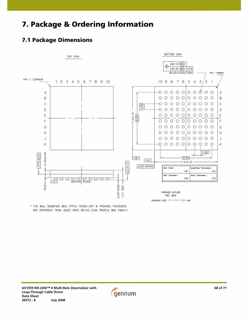
7. Package & Ordering Information
7.1 Package Dimensions
GS1559 HD-LINX™ II Multi-Rate Deserializer with Loop-Through Cable DriverData Sheet30572 - 8 July 2008
68 of 71

7.2 Solder Reflow ProfilesThe GS1559 is available in a Pb or Pb-free package. It is recommended that the Pb package be soldered with Pb paste using the Standard Eutectic profile shown in Figure 7-1, and the Pb-free package be soldered with Pb-free paste using the reflow profile shown in Figure 7-2.
NOTE: It is possible to solder a Pb-free package with Pb paste using a Standard Eutectic profile with a reflow temperature maintained at 245oC – 250oC.
Figure 7-1: Standard Eutectic Solder Reflow Profile (Pb package, Pb paste)
Figure 7-2: Maximum Pb-free Solder Reflow Profile (Pb-free package, Pb-free paste)
25°C
100°C
150°C
183°C
230°C220°C
Time
Temperature
6 min. max
120 sec. max
60-150 sec.
10-20 sec.
3°C/sec max
6°C/sec max
25°C
150°C
200°C
217°C
260°C250°C
Time
Temperature
8 min. max
60-180 sec. max
60-150 sec.
20-40 sec.
3°C/sec max
6°C/sec max
GS1559 HD-LINX™ II Multi-Rate Deserializer with Loop-Through Cable DriverData Sheet30572 - 8 July 2008
69 of 71

7.3 Packaging Data
7.4 Ordering Information
Parameter Value
Package Type 11mm x 11mm 100-ball LBGA
Package Drawing Reference JEDEC M0192
Moisture Saturation Level 3
Junction to Case Thermal Resistance, θj-c 10.4°C/W
Junction to Air Thermal Resistance, θj-a (at zero airflow)
37.1°C/W
Psi 0.4°C/W
Pb-free and RoHS compliant Yes
Part Number Package Pb-free and RoHS Compliant
Temperature Range
GS1559-CBE2 100-ball BGA Yes 0°C to 70°C
GS1559-CB 100-ball BGA No 0°C to 70°C
GS1559 HD-LINX™ II Multi-Rate Deserializer with Loop-Through Cable DriverData Sheet30572 - 8 July 2008
70 of 71

CAUTIONELECTROSTATIC SENSITIVE DEVICES
DO NOT OPEN PACKAGES OR HANDLE EXCEPT AT A STATIC-FREE WORKSTATION
OTTAWA DESIGN CENTRE232 Herzberg Road, Suite 101 Kanata, Ontario K2K 2A1 Canada
Phone: +1 (613) 270-0458
Fax: +1 (613) 270-0429
UNITED KINGDOM DESIGN CENTRENorth Building, Walden Court Parsonage Lane, Bishop’s Stortford Hertfordshire, CM23 6DB Great Britain
Phone: +44 (1279) 714170
Fax: +44 (1279) 714171
JAPAN KKShinjuku Green Tower Building 27F 6-14-1, Nishi Shinjuku Shinjuku-ku, Tokyo, 160-0023 Japan
Phone: +81 (03) 3349 5501
Fax: +81 (03) 3349 5505
Email: [email protected]
Web Site: http://www.gennum.co.jp
SNOWBUSH IP - A DIVISION OF GENNUM439 University Ave. Suite 1700 Toronto, Ontario M5G 1Y8 Canada
Phone: +1 (416) 925-5643
Fax: +1 (416) 925-0581
Web Site: http://www.snowbush.com
AGUASCALLIENTES PHYSICAL DESIGN CENTERVenustiano Carranza 122 Int. 1 Centro, Aguascalientes Mexico CP 20000
Phone: +1 (416) 848-0328
GERMANYNiederlassung Deutschland Stefan-George-Ring 29 81929 München, Germany
Phone: +49 89 309040 290
Fax: +49 89 309040 293
Email: [email protected]
UNITED STATES - WESTERN REGIONBayshore Plaza 2107 N 1st Street, Suite #300 San Jose, CA 95131 United States
Phone: +1 (408) 392-9430
Fax: +1 (408) 392-9404
UNITED STATES - EASTERN REGION4281 Harvester Road Burlington, Ontario L7L 5M4 Canada
Phone: +1 (905) 632-2996
Fax: +1 (905) 632-2055
TAIWAN6F-4, No.51, Sec.2, Keelung Rd. Sinyi District, Taipei City 11502 Taiwan R.O.C.
Phone: (886) 2-8732-8879
Fax: (886) 2-8732-8870
KOREA8F, Jinnex Lakeview Bldg. 65-2, Bangidong, Songpagu Seoul, Korea 138-828
Phone: +82-2-414-2991
Fax: +82-2-414-2998
DOCUMENT IDENTIFICATIONDATA SHEETThe product is in production. Gennum reserves the right to make changes to the product at any time without notice to improve reliability, function or design, in order to provide the best product possible.
GS1559 HD-LINX™ II Multi-Rate Deserializer with Loop-Through Cable DriverData Sheet30572 - 8 July 2008
71 of 7171
Gennum Corporation assumes no liability for any errors or omissions in this document, or for the use of the circuits or devices described herein. The sale of the circuit or device described herein does not imply any patent license, and Gennum makes no representation that the circuit or device is free from patent infringement.
All other trademarks mentioned are the properties of their respective owners.
GENNUM and the Gennum logo are registered trademarks of Gennum Corporation.
© Copyright 2004 Gennum Corporation. All rights reserved. Printed in Canada.
www.gennum.com
GENNUM CORPORATIONMailing Address: P.O. Box 489, Station A, Burlington, Ontario L7R 3Y3 Canada
Street Addresses: 4281 Harvester Road, Burlington, Ontario L7L 5M4 Canada
Phone: +1 (905) 632-2996 Fax: +1 (905) 632-2055
Email: [email protected] www.gennum.com


