H48SC28016 450W DC/DC Power Module
DS_H48SC28016_06132014 E-mail: [email protected]
http://www.deltaww.com/dcdc
P1
FEATURES
High efficiency: 95% @ 28V/16A
Size:
61.0x57.9x11.2mm
(2.40”x2.28”x0.44”) w/o heat-spreader
61.0x57.9x13.2mm
(2.40”x2.28”x0.52”) with heat-spreader
Industry standard footprint and pinout
Fixed frequency operation
Parallel and droop current sharing
Input UVLO
OTP and output OVP
Output OCP hiccup mode
Output voltage trim down : -18%
Output voltage trim up: +18%
Monotonic startup into normal and
pre-biased loads
1500V isolation and basic insulation
No minimum load required
No negative current during power or enable on/off
ISO 9001, TL 9000, ISO 14001, QS 9000,
OHSAS18001 certified manufacturing facility
UL/cUL 60950-1 (US & Canada)
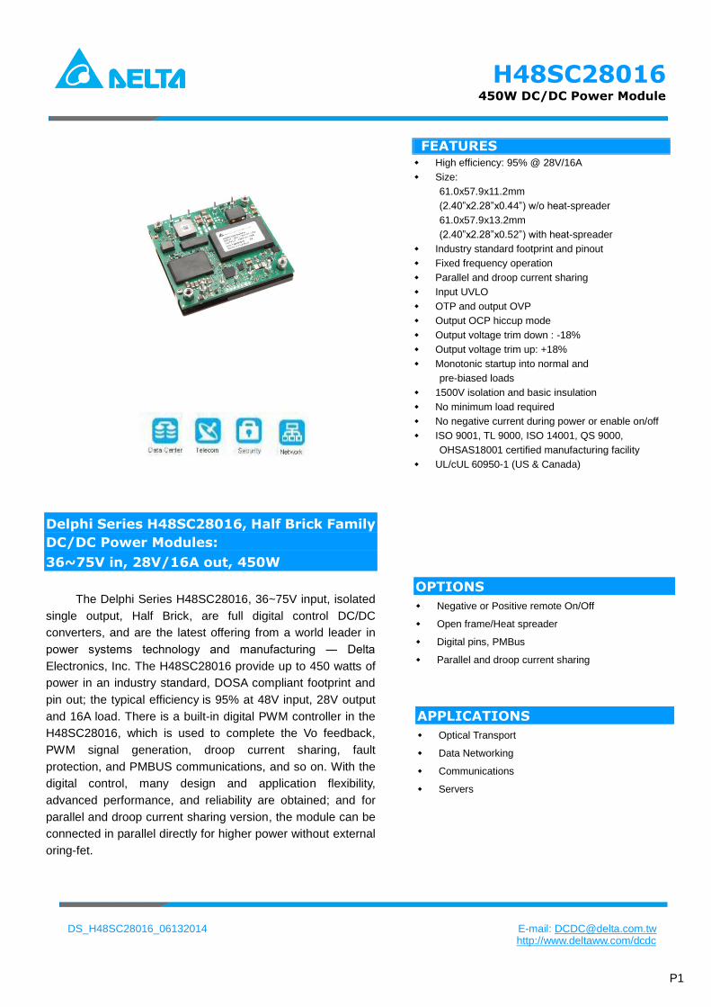
Delphi Series H48SC28016, Half Brick Family
DC/DC Power Modules:
36~75V in, 28V/16A out, 450W
The Delphi Series H48SC28016, 36~75V input, isolated
single output, Half Brick, are full digital control DC/DC
converters, and are the latest offering from a world leader in
power systems technology and manufacturing ― Delta
Electronics, Inc. The H48SC28016 provide up to 450 watts of
power in an industry standard, DOSA compliant footprint and
pin out; the typical efficiency is 95% at 48V input, 28V output
and 16A load. There is a built-in digital PWM controller in the
H48SC28016, which is used to complete the Vo feedback,
PWM signal generation, droop current sharing, fault
protection, and PMBUS communications, and so on. With the
digital control, many design and application flexibility,
advanced performance, and reliability are obtained; and for
parallel and droop current sharing version, the module can be
connected in parallel directly for higher power without external
oring-fet.
APPLICATIONS
Optical Transport
Data Networking
Communications
Servers
OPTIONS
Negative or Positive remote On/Off
Open frame/Heat spreader
Digital pins, PMBus
Parallel and droop current sharing

DS_H48SC28016_06132014 E-mail: [email protected]
http://www.deltaww.com/dcdc P2
TECHNICAL SPECIFICATIONS (TA=25°C, airflow rate=300 LFM, Vin=48Vdc, nominal Vout unless otherwise noted.)
Note1: If the ambient temp is less than 0°C, double minimum output capacitance and additional 50uF ceramic capacitance is necessary.
Note2: For wider output voltage trim range and larger output capacitance, please contact Delta.
PARAMETER NOTES and CONDITIONS H48SC28016 (Standard) Min. Typ. Max. Units
ABSOLUTE MAXIMUM RATINGS
Input Voltage Vdc
Continuous 0 80 Vdc
Transient (100ms) 100ms 100 Vdc
Operating Ambient Temperature -40 85 °C
Storage Temperature -55 125 °C
Input/Output Isolation Voltage 1500 Vdc INPUT CHARACTERISTICS
Operating Input Voltage 36 48 75 Vdc
Input Under-Voltage Lockout
Turn-On Voltage Threshold 33.0 35.0 36.0 Vdc
Turn-Off Voltage Threshold 30.0 33.0 35.0 Vdc
Lockout Hysteresis Voltage 1 2 3 Vdc
Maximum Input Current Full Load, 36Vin 17 A
No-Load Input Current Vin=48V, Io=0A 110 mA
Off Converter Input Current Vin=48V, Io=0A 22 mA
Inrush Current ( I2t) 1 A
2s
Input Reflected-Ripple Current P-P thru 12µH inductor, 5Hz to 20MHz 80 mA
Input Voltage Ripple Rejection 120 Hz 50 dB OUTPUT CHARACTERISTICS
Output Voltage Set Point Vin=48V, Io=Io.max, Tc=25°C 27.72 28 28.28 Vdc
Output Regulation
Over Load Io=Io, min to Io, max ±56 mV
Over Line Vin=36V to 75V ±56 mV
Over Temperature Tc=-40°C to 85°C ±560 mV
Total Output Voltage Range Over sample load, line and temperature 27.16 28.84 V
Output Voltage Ripple and Noise 5Hz to 20MHz bandwidth
Peak-to-Peak Vin=48V, Full Load, 50µF ceramic, 1000uF Electrolytic Capacitor 100 mV
RMS Vin=48V, Full Load, 50µF ceramic, 1000uF Electrolytic Capacitor 30 mV
Operating Output Current Range Vin=36V to75V 0 16 A
Output Over Current Protection(hiccup mode) Output Voltage 10% Low 17.6 24 A DYNAMIC CHARACTERISTICS
Output Voltage Current Transient 48Vin, 50µF ceramic, 1000uF Electrolytic Capacitor, 0.1A/µs
Positive Step Change in Output Current 75% Io.max to 50% Io.max 300 mV
Negative Step Change in Output Current 50% Io.max to 75% Io.max 300 mV
Settling Time (within 1% Vout nominal) 200 µs
Turn-On Transient
Start-Up Time, From On/Off Control 80 mS
Start-Up Time, From Input 100 mS
Output Capacitance (note1) Full load; 5% overshoot of Vout at startup, low ESR cap. 470 5000 µF EFFICIENCY
100% Load Vin=36V 94.5 %
100% Load Vin=48V 95 %
60% Load Vin=48V 95.5 % ISOLATION CHARACTERISTICS
Input to Output 1500 Vdc
Isolation Resistance 10 MΩ
Isolation Capacitance 6.9 nF FEATURE CHARACTERISTICS
Switching Frequency 120 KHz
ON/OFF Control, Negative Remote On/Off logic
Logic Low (Module On) Von/off 0.8 V
Logic High (Module Off) Von/off 3.5 10 V
ON/OFF Control, Positive Remote On/Off logic
Logic Low (Module Off) Von/off 0.8 V
Logic High (Module On) Von/off 3.5 10 V
ON/OFF Current (for both remote on/off logic) Ion/off at Von/off=0.0V mA
Leakage Current (for both remote on/off logic) Logic High, Von/off=5V
Output Voltage Trim Range (note2) Pout ≦ max rated power,Io ≦ Io.max -18 +18 %
Output Voltage Remote Sense Range Pout ≦ max rated power,Io ≦ Io.max -3 +10 %
Output Over-Voltage Protection % of nominal Vout 125 150 %
GENERAL SPECIFICATIONS
MTBF Io=80% of Io, max; Ta=25°C, airflow rate=300LFM 2.9 Mhours hours Weight Without heat spreader 62.0 grams
Weight With heat spreader 93.5 grams
Over-Temperature Shutdown (With heat spreader) Refer to Figure 18 for Hot spot location (48Vin,80% Io) 110 °C
Over-Temperature Shutdown ( NTC resistor ) 125 °C
Note: Please attach thermocouple on NTC resistor to test OTP function, the hot spots’ temperature is just for reference.

DS_H48SC28016_06132014 E-mail: [email protected]
http://www.deltaww.com/dcdc P3
ELECTRICAL CHARACTERISTICS CURVES
Figure 1: Efficiency vs. load current for 36V, 48V, and 75V input voltage at 25°C.
Figure 2: Power dissipation vs. load current for 36V, 48V, and 75V input voltage at 25°C.
Figure 3: Full load input characteristics at room temperature.
DS_H48SC28016_06132014 E-mail: [email protected]
http://www.deltaww.com/dcdc P4
ELECTRICAL CHARACTERISTICS CURVES
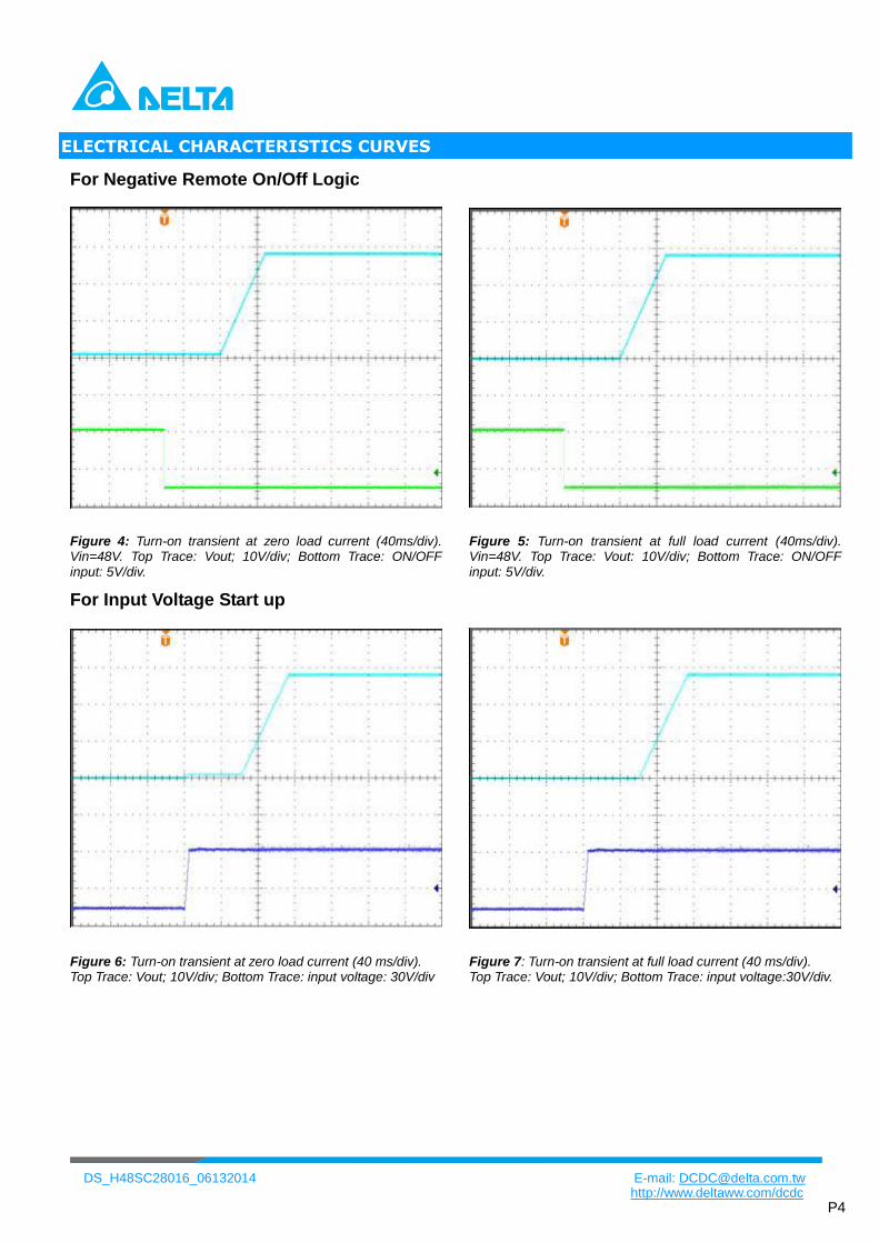
For Negative Remote On/Off Logic
Figure 4: Turn-on transient at zero load current (40ms/div). Vin=48V. Top Trace: Vout; 10V/div; Bottom Trace: ON/OFF input: 5V/div.
Figure 5: Turn-on transient at full load current (40ms/div). Vin=48V. Top Trace: Vout: 10V/div; Bottom Trace: ON/OFF input: 5V/div.
For Input Voltage Start up
Figure 6: Turn-on transient at zero load current (40 ms/div). Top Trace: Vout; 10V/div; Bottom Trace: input voltage: 30V/div
Figure 7: Turn-on transient at full load current (40 ms/div). Top Trace: Vout; 10V/div; Bottom Trace: input voltage:30V/div.

DS_H48SC28016_06132014 E-mail: [email protected]
http://www.deltaww.com/dcdc P5
ELECTRICAL CHARACTERISTICS CURVES
Figure 8: Output voltage response to step-change in load current (50%-75% of Io, max; di/dt = 0.1A/µs; Vin=48V). Load cap: 1000µF Electrolytic Capacitor and 50µF ceramic capacitor. Top Trace: Vout (0.2V/div, 200us/div), Bottom Trace: Iout (5A/div). Scope measurement should be made using a BNC cable (length shorter than 20 inches). Position the load between 51 mm to 76 mm (2 inches to 3 inches) from the module
Figure 9: Output voltage response to step-change in load current (75%-50% of Io, max; di/dt = 0.1A/µs; Vin=48V). Load cap: 1000µF Electrolytic Capacitor and 50µF ceramic capacitor. Top Trace: Vout (0.2V/div, 200us/div), Bottom Trace: Iout (5A/div). Scope measurement should be made using a BNC cable (length shorter than 20 inches). Position the load between 51 mm to 76 mm (2 inches to 3 inches) from the module
Figure 10: Test set-up diagram showing measurement points for Input Terminal Ripple Current and Input Reflected Ripple Current. Note: Measured input reflected-ripple current with a simulated source Inductance (LTEST) of 12 μH. Capacitor Cs offset possible battery impedance. Measure current as shown above.
Figure 11: Input Terminal Ripple Current, ic, at max output current and nominal input voltage with 12µH source impedance
and 100µF electrolytic capacitor (500 mA/div,4us/div).
100uF
DS_H48SC28016_06132014 E-mail: [email protected]
http://www.deltaww.com/dcdc P6
ELECTRICAL CHARACTERISTICS CURVES
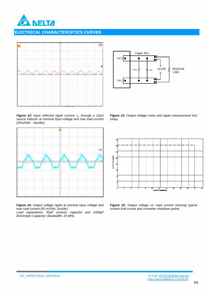
Figure 12: Input reflected ripple current, is, through a 12µH source inductor at nominal input voltage and max load current
(25mA/div,4us/div).
Figure 13: Output voltage noise and ripple measurement test setup.
Figure 14: Output voltage ripple at nominal input voltage and max load current (50 mV/div, 2us/div) Load capacitance: 50µF ceramic capacitor and 1000µF Electrolytic Capacitor. Bandwidth: 20 MHz.
Figure 15: Output voltage vs. load current showing typical current limit curves and converter shutdown points.

DS_H48SC28016_06132014 E-mail: [email protected]
http://www.deltaww.com/dcdc P7
DESIGN CONSIDERATIONS
Input Source Impedance The impedance of the input source connecting to the DC/DC power modules will interact with the modules and affect the stability. A low ac-impedance input source is recommended. If the source inductance is more than a few μH, we advise 220μF electrolytic capacitor (ESR < 0.7 Ω at 100 kHz) mounted close to the input of the module to improve the stability.
Layout and EMC Considerations Delta’s DC/DC power modules are designed to operate in a wide variety of systems and applications. For design assistance with EMC compliance and related PWB layout issues, please contact Delta’s technical support team. An external input filter module is available for easier EMC compliance design. Below is the reference design for an input filter tested with H48SC28016 to meet class B in CISSPR 22.
Schematic and Components List
4.7uPA2416
(Pulse)
100n
10u
100n
100n
100n
100n 470u*2PA2416
(Pulse)
INPUT+
INPUT-
Vin+
Vin-
Vout+
Vout-
MODULE
750uH 750uH
Test Result:Vin=48V,Io=16A
1 MHz 10 MHz150 kHz 30 MHz
10.0
20.0
30.0
40.0
50.0
60.0
70.0
0.0
80.0
dBμV
Limits
55022MQP
55022MAV
�
Transducer
8130
Traces
PK+
AV
Blue Line is quasi peak mode;green line is average mode.
Safety Considerations The power module must be installed in compliance with the spacing and separation requirements of the end-user’s safety agency standard, i.e., UL60950-1, CSA C22.2 NO. 60950-1 2nd and IEC 60950-1 2nd : 2005 and EN 60950-1 2nd: 2006+A11+A1: 2010, if the system in which the power module is to be used must meet safety agency requirements. Basic insulation based on 75 Vdc input is provided between the input and output of the module for the purpose of applying insulation requirements when the input to this DC-to-DC converter is identified as TNV-2 or SELV. An additional evaluation is needed if the source is other than TNV-2 or SELV. When the input source is SELV circuit, the power module meets SELV (safety extra-low voltage) requirements. If the input source is a hazardous voltage which is greater than 60 Vdc and less than or equal to 75 Vdc, for the module’s output to meet SELV requirements, all of the following must be met: The input source must be insulated from the ac
mains by reinforced or double insulation. The input terminals of the module are not operator
accessible. A SELV reliability test is conducted on the system
where the module is used, in combination with the module, to ensure that under a single fault, hazardous voltage does not appear at the module’s output.
When installed into a Class II equipment (without grounding), spacing consideration should be given to the end-use installation, as the spacing between the module and mounting surface have not been evaluated. The power module has extra-low voltage (ELV) outputs when all inputs are ELV. This power module is not internally fused. To achieve optimum safety and system protection, an input line fuse is highly recommended. The safety agencies require a normal-blow fuse with 50A maximum rating to be installed in the ungrounded lead. A lower rated fuse can be used based on the maximum inrush transient energy and maximum input current.
Soldering and Cleaning Considerations Post solder cleaning is usually the final board assembly process before the board or system undergoes electrical testing. Inadequate cleaning and/or drying may lower the reliability of a power module and severely affect the
DS_H48SC28016_06132014 E-mail: [email protected]
http://www.deltaww.com/dcdc P8
reliability of a power module and severely affect the finished circuit board assembly test. Adequate cleaning and/or drying is especially important for un-encapsulated and/or open frame type power modules. For assistance on appropriate soldering and cleaning procedures, please contact Delta’s technical support team.
FEATURES DESCRIPTIONS
Over-Current Protection
The modules include an internal output over-current protection circuit, which will endure current limiting for an unlimited duration during output overload. If the output current exceeds the OCP set point, the modules will shut down (hiccup mode). The modules will try to restart after shutdown. If the overload condition still exists, the module will shut down again. This restart trial will continue until the overload condition is corrected.
Over-Voltage Protection
The modules include an internal output over-voltage protection circuit, which monitors the voltage on the output terminals. If this voltage exceeds the over-voltage set point, the protection circuit will constrain the max duty cycle to limit the output voltage, if the output voltage continuously increases the modules will shut down, and then restart after a hiccup-time (hiccup mode).
Over-Temperature Protection
The over-temperature protection consists of circuitry that provides protection from thermal damage. If the temperature exceeds the over-temperature threshold the module will shut down.The module will restart after the temperature is within specification.
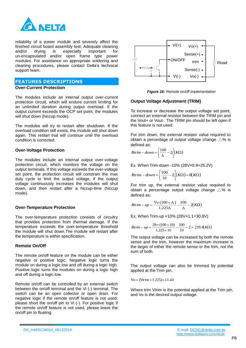
Remote On/Off
The remote on/off feature on the module can be either negative or positive logic. Negative logic turns the module on during a logic low and off during a logic high. Positive logic turns the modules on during a logic high and off during a logic low. Remote on/off can be controlled by an external switch between the on/off terminal and the Vi (-) terminal. The switch can be an open collector or open drain. For negative logic if the remote on/off feature is not used, please short the on/off pin to Vi (-). For positive logic if the remote on/off feature is not used, please leave the on/off pin to floating.
Vo(+)
Sense(+)
Vo(-)
trim
Vi(+)
Vi(-)
ON/OFFRload
Sense(-)
Figure 16: Remote on/off implementation
Output Voltage Adjustment (TRIM) To increase or decrease the output voltage set point, connect an external resistor between the TRIM pin and the Vout+ or Vout-. The TRIM pin should be left open if this feature is not used. For trim down, the external resistor value required to
obtain a percentage of output voltage change △% is
defined as:
KdownRtrim 2
100
Ex. When Trim-down -10% (28V×0.9=25.2V)
KKdownRtrim 82
10
100
For trim up, the external resistor value required to
obtain a percentage output voltage change △% is
defined as:
KupRtrim 2
100
1.225
) (100 Vo
Ex. When Trim-up +10% (28V×1.1=30.8V)
KupRtrim 4.2392
10
100
10225.1
)10100(28
The output voltage can be increased by both the remote sense and the trim, however the maximum increase is the larger of either the remote sense or the trim, not the sum of both. The output voltage can also be trimmed by potential applied at the Trim pin.
11.431.225)(o VtrimV
Where trim Vtrim is the potential applied at the Trim pin, and Vo is the desired output voltage.
DS_H48SC28016_06132014 E-mail: [email protected]
http://www.deltaww.com/dcdc P9
When using remote sense and trim, the output voltage of the module is usually increased, which increases the power output of the module with the same output current. Care should be taken to ensure that the maximum output power of the module remains at or below the maximum rated power.
THERMAL CONSIDERATIONS
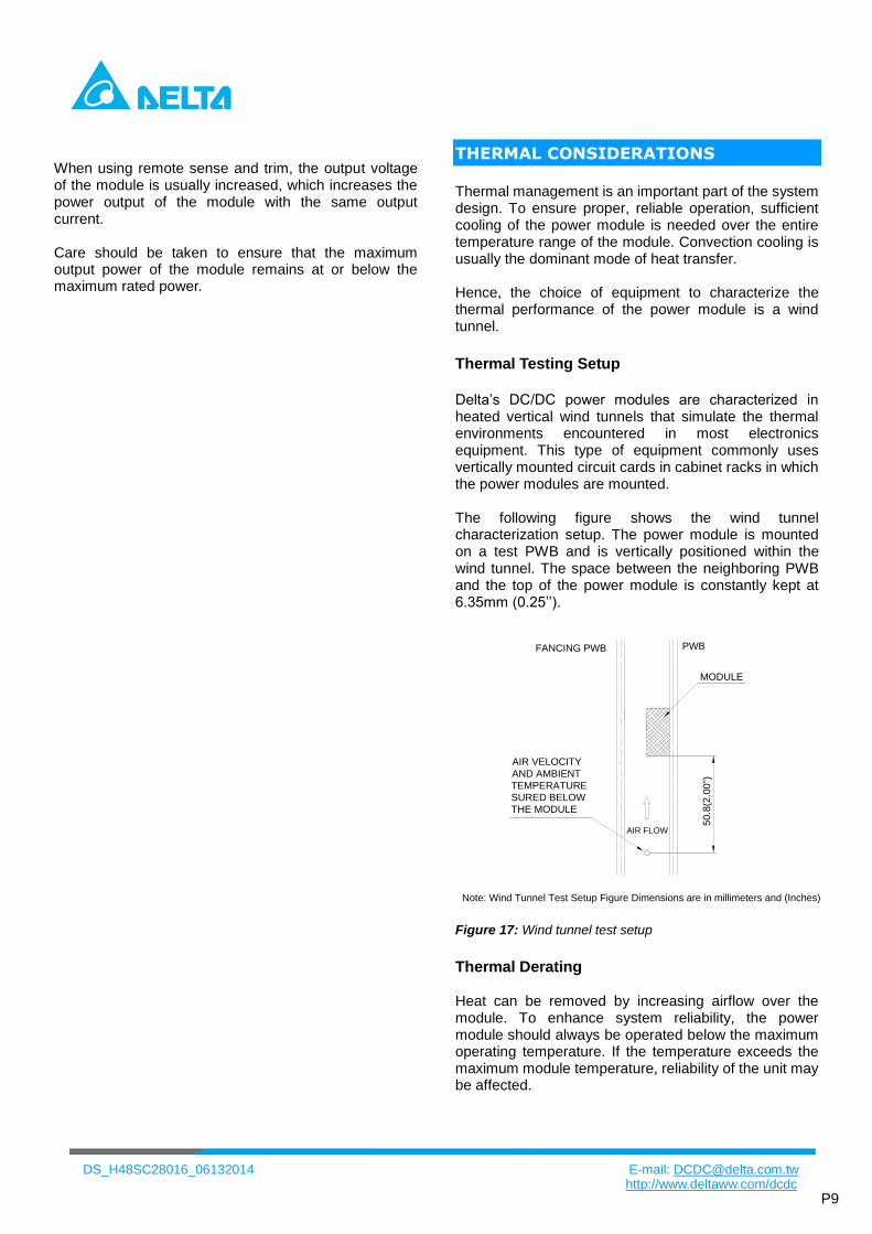
Thermal management is an important part of the system design. To ensure proper, reliable operation, sufficient cooling of the power module is needed over the entire temperature range of the module. Convection cooling is usually the dominant mode of heat transfer. Hence, the choice of equipment to characterize the thermal performance of the power module is a wind tunnel.
Thermal Testing Setup Delta’s DC/DC power modules are characterized in heated vertical wind tunnels that simulate the thermal environments encountered in most electronics equipment. This type of equipment commonly uses vertically mounted circuit cards in cabinet racks in which the power modules are mounted. The following figure shows the wind tunnel characterization setup. The power module is mounted on a test PWB and is vertically positioned within the wind tunnel. The space between the neighboring PWB and the top of the power module is constantly kept at 6.35mm (0.25’’).
AIR FLOW
MODULE
PWB
50
.8(2
.00")
AIR VELOCITY
AND AMBIENT
TEMPERATURE
SURED BELOW
THE MODULE
FANCING PWB
Note: Wind Tunnel Test Setup Figure Dimensions are in millimeters and (Inches)
Figure 17: Wind tunnel test setup
Thermal Derating
Heat can be removed by increasing airflow over the module. To enhance system reliability, the power module should always be operated below the maximum operating temperature. If the temperature exceeds the maximum module temperature, reliability of the unit may be affected.

DS_H48SC28016_06132014 E-mail: [email protected]
http://www.deltaww.com/dcdc P10
THERMAL CURVES
(ATTACH TO COLD PLATE)
Vin(+)
ON/OFF
CASE
Vin(-)
SENSE(-)
Vout(-)
TRIM
SENSE(+)
Vout(+)
Figure 18: *Temperature measurement location viewed from
top side. The allowed maximum hot spot temperature is defined
at 100℃.
0
50
100
150
200
250
300
350
400
450
500
25 30 35 40 45 50 55 60 65 70 75 80 85 90 95 100 105
H48SC28016(Standard) Output Power vs. Hot Spot Temperature@Vin = 48V (Either Orientation,With Heatspreader)
Hot Spot Temperature (℃)
Output Power (W)
Figure 19: Output power vs. Hot spot temperature @Vin=48V (Either Orientation)

DS_H48SC28016_06132014 E-mail: [email protected]
http://www.deltaww.com/dcdc P11
MECHANICAL DRAWING (WITH HEAT SPREADER)
For modules with through-hole pins and the optional heatspreader, they are intended for wave soldering assembly
onto system boards; please do not subject such modules through reflow temperature profile.
DS_H48SC28016_06132014 E-mail: [email protected]
http://www.deltaww.com/dcdc P12
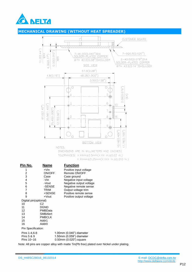
MECHANICAL DRAWING (WITHOUT HEAT SPREADER)
Pin No. Name Function
1 2 3 4 5 6 7 8 9
+Vin ON/OFF Case -Vin -Vout -SENSE TRIM +SENSE +Vout
Positive input voltage Remote ON/OFF Case ground Negative input voltage Negative output voltage Negative remote sense Output voltage trim Positive remote sense Positive output voltage
Digital pin(optional) 10 11 12 13 14 15 16
C2 DGND PMBData SMBAlert PMBCLK Addr1 Addr0
Pin Specification:
Pins 1-4,6-8 1.00mm (0.040”) diameter Pins 5 & 9 1.50mm (0.059”) diameter Pins 10~16 2. 0.50mm (0.020”) square
Note: All pins are copper alloy with matte Tin(Pb free) plated over Nickel under plating.

DS_H48SC28016_06132014 E-mail: [email protected]
http://www.deltaww.com/dcdc P14
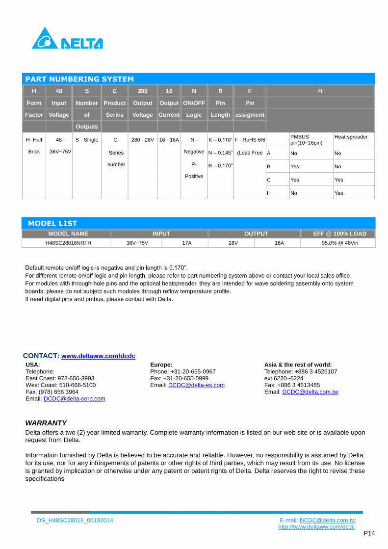
PART NUMBERING SYSTEM
H 48 S C 280 16 N R F H
Form
Factor
Input
Voltage
Number
of
Outputs
Product
Series
Output
Voltage
Output
Current
ON/OFF
Logic
Pin
Length
Pin
assigment
H- Half
Brick
48 -
36V~75V
S - Single C-
Series
number
280 - 28V 16 - 16A
N -
Negative
P-
Positive
K – 0.110”
N – 0.145”
R – 0.170”
F - RoHS 6/6
(Lead Free
PMBUS pin(10~16pin)
Heat spreader
A No No
B Yes No
C Yes Yes
H No Yes
MODEL LIST
MODEL NAME INPUT OUTPUT EFF @ 100% LOAD
H48SC28016NRFH 36V~75V 17A 28V 16A 95.0% @ 48Vin
Default remote on/off logic is negative and pin length is 0.170”.
For different remote on/off logic and pin length, please refer to part numbering system above or contact your local sales office.
For modules with through-hole pins and the optional heatspreader, they are intended for wave soldering assembly onto system
boards; please do not subject such modules through reflow temperature profile.
If need digital pins and pmbus, please contact with Delta.
CONTACT: www.deltaww.com/dcdc
USA:
Telephone: East Coast: 978-656-3993 West Coast: 510-668-5100 Fax: (978) 656 3964 Email: [email protected]
Europe:
Phone: +31-20-655-0967 Fax: +31-20-655-0999 Email: [email protected]
Asia & the rest of world:
Telephone: +886 3 4526107 ext 6220~6224 Fax: +886 3 4513485 Email: [email protected]
WARRANTY
Delta offers a two (2) year limited warranty. Complete warranty information is listed on our web site or is available upon request from Delta.
Information furnished by Delta is believed to be accurate and reliable. However, no responsibility is assumed by Delta
for its use, nor for any infringements of patents or other rights of third parties, which may result from its use. No license
is granted by implication or otherwise under any patent or patent rights of Delta. Delta reserves the right to revise these
specifications


