
HT8 MCU Integrated DAC Application Guideline – Voice Application
AN0466E 1 / 7 November 11, 2017
HT8 MCU Integrated DAC Application Guideline – Voice Application
D/N: AN0466E
Introduction Holtek’s Voice devices include the HT83F02 which has an integrated Delta Sigma PWM
driver which can directly drive speakers. There is also the HT83F22, HT66FV1x0 and
BS66FV3x0 series which include an integrated R-2R DAC and Class AB Audio Power
Amplifier. With respect to the latter series, their voice function is implemented using a
DAC to generate the voice analog signals which then are amplified by the power amplifier
to drive speakers. The DAC resolution determines the smoothness of the voice output.
Holtek’s Voice MCUs cover both 12-bit and 16-bit DAC specifications and also provide
other necessary peripherals to meet different product requirements. To provide users with
a practical guide, this application note will use Holtek’s Voice MCU, the HT66FV140, as
an example to introduce the operating principles of its integrated R-2R DAC from.
Functional Description Commonly used DACs can be divided into five types, the R-2R ladder resistor network
DAC, the weighted resistance network DAC, the inverted R-2R ladder resistor network
DAC, the weighted current DAC and the Delta Sigma DAC. With the need for higher
quality audio the DAC specifications have consequently gradually improved. Higher DAC
resolution results in smaller signal distortion thus resulting in better sound quality. The
following provides a description of the common R-2R ladder resistor network DAC.
(1) R-2R architecture DAC basic principle description
8-bit R-2R Resistor Network DAC Conversion Circuit

HT8 MCU Integrated DAC Application Guideline – Voice Application
AN0466E 2 / 7 November 11, 2017
As shown in the above figure, VREF on the left is the DAC reference voltage input.
Each 2R branch is connected to a SPDT (Single-Pole Double-Throw) switch, which
controls whether the branch is connected to the operational amplifier inverting input
or to ground. The switching direction of the SPDT switch is determined by the DAC
input digital signal. The MSB of the 8-bit DAC digital signal is on the leftmost, and the
LSB is on the rightmost. For example, if using the sequence of D7, D6, D5, D4, D3,
D2, D1, D0 to express the 8-bit DAC data, the MSB is D7 and the LSB is D0. The
LSB branch SPDT switch is controlled by D0. The LSB branch is connected to the
operational amplifier inverting input when D0 is equal to 1 and to ground when D0
equals 0. This also applies to the other branches. According to the R-2R resistor
network superposition principle, the overall output current IOUT of the resistor network
is calculated as below:
𝐼𝐼OUT =𝑉𝑉REF𝑅𝑅 �
𝐷𝐷028 +
𝐷𝐷127 + ⋯+
𝐷𝐷622 +
𝐷𝐷721� =
𝑉𝑉REF28 × 𝑅𝑅�(𝐷𝐷i × 2𝑖𝑖)
7
𝑖𝑖=0
After the operational amplifier, the output analog voltage VOUT is:
𝑉𝑉OUT = −𝐼𝐼OUT × 𝑅𝑅fb = −𝑅𝑅fbR ×
𝑉𝑉REF28 �(𝐷𝐷i × 2𝑖𝑖)
7
𝑖𝑖=0
From the output formula provided above, the output voltage VOUT is proportional to
the input DAC value, i.e., the larger the input DAC value is, the higher the output
analog voltage VOUT will be.
(2) DAC application specification
Taking the HT66FV140 as an example, its voice development platform supports
HT-ADPCM4, HT-UPCM8, HT-PCM12 and HT-PCM16 four voice coding formats.
The table below shows the maximum sampling frequencies of each coding format
voice file corresponding to different MCU system frequencies.
System Freq. Coding Mode 8MHz 12MHz 16MHz
HT-ADPCM4 14kHz 21kHz 28kHz HT-UPCM8 17kHz 26kHz 35kHz HT-PCM12 18kHz 27kHz 36kHz HT-PCM16 19kHz 29kHz 39kHz
(3) DAC voice playing control diagram
Voice Playing Control Diagram

HT8 MCU Integrated DAC Application Guideline – Voice Application
AN0466E 3 / 7 November 11, 2017
The HT66FV140 contains a fully integrated 16-bit DAC complete with volume control
together with a power amplifier. The voice data placed in the PLADH and PLADL
registers can be output to the power amplifier via the DAC and then the power
amplifier can drive the external speakers. The volume control can be adjusted using
the USVC[6:0] bits with a range of -32dB to 6dB.
(4) DAC control register description
The voice playing function of the HT66FV140 is controlled using a series of registers.
Two control registers exist to control the 16-bit DAC and power amplifier functions
together with the speaker mute control. Two data register pairs exist to store the data
which is to be played. The detailed register names and bit definitions are shown below.
Register Name
Bit 7 6 5 4 3 2 1 0
USVC MUTEB USVC6 USVC5 USVC4 USVC3 USVC2 USVC1 USVC0 PLAC — — — — — — PAEN DAEN PLADL P_D7 P_D6 P_D5 P_D4 P_D3 P_D2 P_D1 P_ D0 PLADH P_D15 P_D14 P_D13 P_D12 P_D11 P_D10 P_D9 P_D8
DAC Control Registers List
USVC is an 8-bit register whose MSB, MUTEB, is used to enable or disable the
speaker output function. When this bit equals 0, both the DAC and the power
amplifier are disabled and the speaker is turned off. When this bit equals 1, both the
DAC and the power amplifier are enabled and the speaker is turned on. The speaker
output volume which ranges from -32dB to 6dB is controlled by the USVC6~USVC0
bits. Detailed volume control configuration is provided below.
Output Volume Control

HT8 MCU Integrated DAC Application Guideline – Voice Application
AN0466E 4 / 7 November 11, 2017
The PAEN bit in the PLAC register is used to enable the power amplifier and the
DAEN bit is used to enable the DAC. When the MCU enters the power down mode,
both the DAC and the power amplifier will be automatically disabled. The PLADH and
PLADL register are used to store the 16-bit play data high and low byte respectively.
Note that if it is required to update this pair of play data registers, the low byte should
be written first after which the high byte should be written.
Operating Principle
The voice playing function of voice type ICs is essentially a digital to analog conversion
process. The pre-processed voice data is converted into an analog signal by the DAC,
which is then amplified by the power amplifier and output to the speaker. Regarding the
voice data pre-processing, it includes voice signal acquisition, coding, equalizer processing,
etc., which are completed using a computer. The digital to analog conversion process of
Holtek’s voice ICs is given in the figure above. By placing the pre-processed voice digital
data into the PLADH and PLADL register pair, adjusting the volume using the USVC bit field
and enabling the DAC, the voice signal can be output on the AUD pin. Using an RC filter
and a coupling capacitor the DAC output signal can be transferred to the power amplifier to
implement a voice playing function.
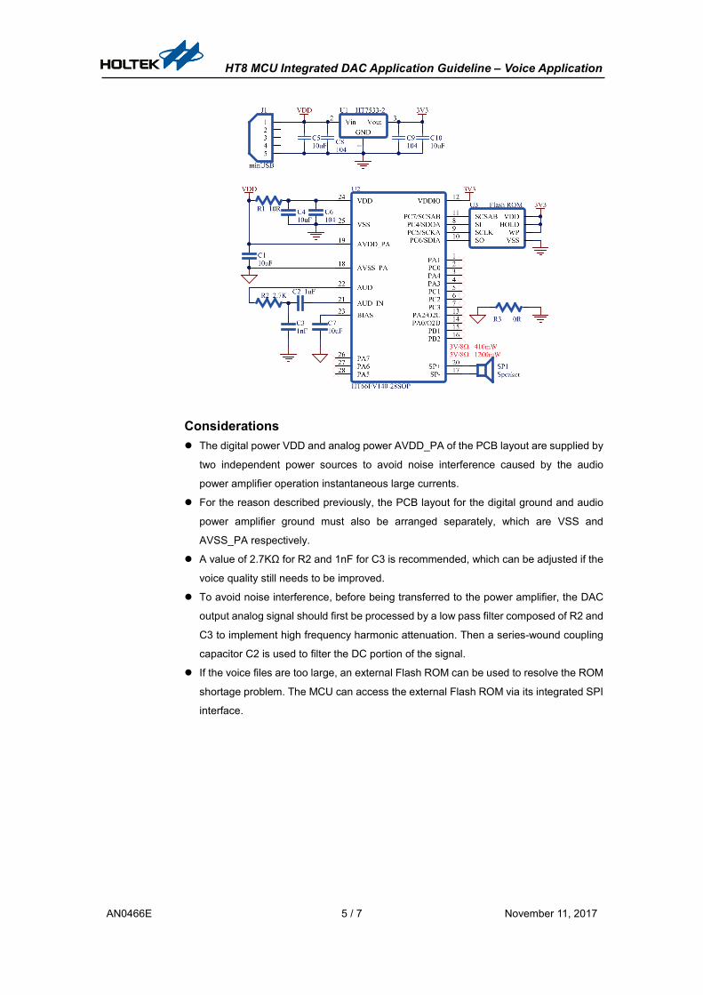
Hardware Description The integrated power amplifier within Holtek’s HT66FV140 voice MCU is shown in the
following figure. The MCU reads the voice data from the Flash ROM via the SPI interface.
The voice data is first converted by the DAC and then output on the AUD pin. After being
filtered by the RC filter composed of R2 and C3, the voice signal will be coupled to the
AUD_IN pin by C2 and then input to the internal power amplifier. The voice signal
amplified by the power amplifier is output to the speaker from the SP+ pin and then
returned to the internal speaker ground from the SP- pin.
HT8 MCU Integrated DAC Application Guideline – Voice Application
AN0466E 5 / 7 November 11, 2017
Considerations The digital power VDD and analog power AVDD_PA of the PCB layout are supplied by
two independent power sources to avoid noise interference caused by the audio
power amplifier operation instantaneous large currents.
For the reason described previously, the PCB layout for the digital ground and audio
power amplifier ground must also be arranged separately, which are VSS and
AVSS_PA respectively.
A value of 2.7KΩ for R2 and 1nF for C3 is recommended, which can be adjusted if the
voice quality still needs to be improved.
To avoid noise interference, before being transferred to the power amplifier, the DAC
output analog signal should first be processed by a low pass filter composed of R2 and
C3 to implement high frequency harmonic attenuation. Then a series-wound coupling
capacitor C2 is used to filter the DC portion of the signal.
If the voice files are too large, an external Flash ROM can be used to resolve the ROM
shortage problem. The MCU can access the external Flash ROM via its integrated SPI
interface.
HT8 MCU Integrated DAC Application Guideline – Voice Application
AN0466E 6 / 7 November 11, 2017
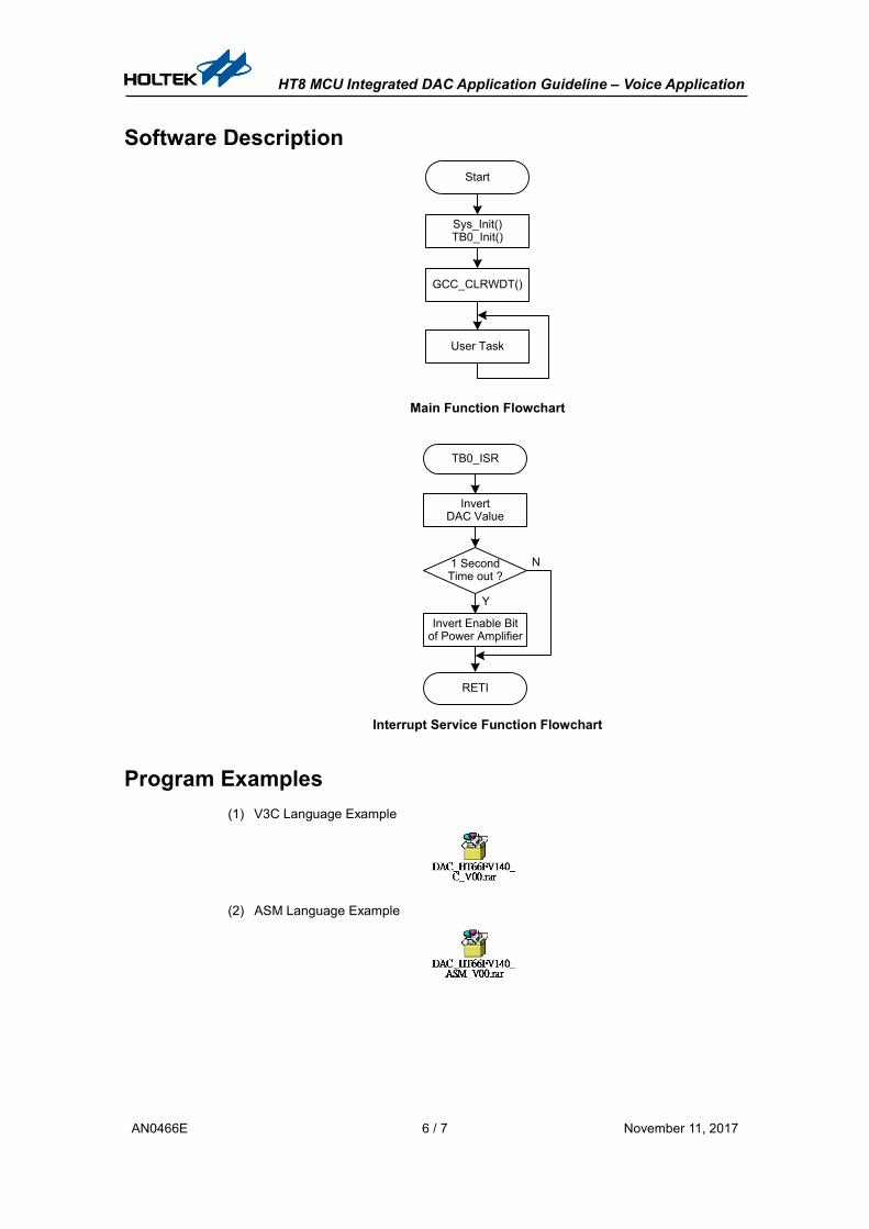
Software Description Start
Sys_Init()TB0_Init()
GCC_CLRWDT()
User Task
Main Function Flowchart
TB0_ISR
1 SecondTime out ?
Invert Enable Bitof Power Amplifier
RETI
Y
N
InvertDAC Value
Interrupt Service Function Flowchart
Program Examples (1) V3C Language Example
(2) ASM Language Example
HT8 MCU Integrated DAC Application Guideline – Voice Application
AN0466E 7 / 7 November 11, 2017
Conclusion
With the DAC usage tips and considerations summarised together with the program
examples provided in this application note, users should be better equipped to use the
DAC function more flexibly.
Versions and Modification Information Date Author Issue Release and Modification
2017.10.26 李昱緯 First Version
Disclaimer
All information, trademarks, logos, graphics, videos, audio clips, links and other items
appearing on this website ('Information') are for reference only and is subject to change at
any time without prior notice and at the discretion of Holtek Semiconductor Inc.
(hereinafter 'Holtek', 'the company', 'us', 'we' or 'our'). Whilst Holtek endeavors to ensure
the accuracy of the Information on this website, no express or implied warranty is given
by Holtek to the accuracy of the Information. Holtek shall bear no responsibility for any
incorrectness or leakage.
Holtek shall not be liable for any damages (including but not limited to computer virus,
system problems or data loss) whatsoever arising in using or in connection with the use of
this website by any party. There may be links in this area, which allow you to visit the
websites of other companies. These websites are not controlled by Holtek. Holtek will
bear no responsibility and no guarantee to whatsoever Information displayed at such sites.
Hyperlinks to other websites are at your own risk.
Limitation of Liability In any case, the Company has no need to take responsibility for any loss or damage
caused when anyone visits the website directly or indirectly and uses the contents,
information or service on the website.
Governing Law This disclaimer is subjected to the laws of the Republic of China and under the jurisdiction
of the Court of the Republic of China.
Update of Disclaimer Holtek reserves the right to update the Disclaimer at any time with or without prior notice,
all changes are effective immediately upon posting to the website.


