
Clemson UniversityTigerPrints
All Dissertations Dissertations
8-2007
Improving the Performance of Software DefinedRadio by Employing Digital Feedback of RadioFrequency PropertiesJoel SimoneauClemson University, [email protected]
Follow this and additional works at: https://tigerprints.clemson.edu/all_dissertations
Part of the Electrical and Computer Engineering Commons
This Dissertation is brought to you for free and open access by the Dissertations at TigerPrints. It has been accepted for inclusion in All Dissertations byan authorized administrator of TigerPrints. For more information, please contact [email protected].
Recommended CitationSimoneau, Joel, "Improving the Performance of Software Defined Radio by Employing Digital Feedback of Radio FrequencyProperties" (2007). All Dissertations. 227.https://tigerprints.clemson.edu/all_dissertations/227

IMPROVING THE PERFORMANCE OF SOFTWARE DEFINED RADIO BY EMPLOYING DIGITAL FEEDBACK OF RADIO
FREQUENCY PROPERTIES
A Dissertation Presented to
the Graduate School of Clemson University
In Partial Fulfillment of the Requirements for the Degree
Doctor of Philosophy Electrical Engineering
by Joel B. Simoneau
August 2007
Accepted by: L. Wilson Pearson, Committee Chair
Carl Baum Pingshan Wang
Nader Jalili

ii

iii
ABSTRACT
This dissertation provides tools for the analysis and integration of the hardware
and software components of a software defined radio for optimum radio frequency
performance. A device is introduced that is able to give baseband feedback of radio
frequency properties suitable for analysis in software. Three applications for the device
are devised. The first is an image rejection upconverter that achieves greater than 65 dB
of image rejection over a broad frequency range without the use of a radio frequency
filter. The second application is a baseband correction scheme for extending the
bandwidth and improving the magnitude and phase match of an off-the-shelf IQ mixer.
The third application is a receive filter that can reject a near-band, high-power interferer
again without the use of a radio frequency filter. The theoretical development and
experimental verification of each system is included.

iv

v
DEDICATION
I am a man well-loved. That love has come from many directions. I tasted this
love first through my loving parents, Jim and Susan, as they patiently trained me through
many years, and pointed me in the way of love. My faithful wife, Hayley, has been my
partner throughout this work and her love has been a calm amidst the storm of preparing
it. My two daughters, Madelyn and Susannah, have filled my heart with joy to see them
grow in every way.
This love has come from many directions; it has but one source: my Lord and
Savior Jesus. It is to this love that is willing to give its own life to save sinners that I
dedicate this work. I pray that it would be a fitting tribute to His work in my life and this
world.

vi

vii
ACKNOWLEDGMENTS
I would like to gratefully acknowledge the members of my committee for their aid
in preparing this document. I would especially like to acknowledge my advisor Professor
L. Wilson Pearson for both the guiding hand and freedom that he has allotted to me
generously during my time as a graduate student. Being under his tutelage has truly been
a pleasure and honor. I would also like to acknowledge James McChesney, who planted
the seeds of this work by pointing me to the work of Vasudev and Collins, along with the
paradigm of baseband compensation for radio frequency performance.
I also owe a debt of gratitude to the Dean’s Fellowship, Holcombe Fellowship,
and the Center for Research in Wireless Communications at Clemson University. The
funding provided by these sources has enabled me to focus on excellence in my research
and has provided me with the tools I needed to keep up with the state of the art.
I would also like to acknowledge my fellow graduate students who have spent a
great deal of time listening to me talk about the work contained herein and offered their
welcome advice. I would especially like to acknowledge Venkatesh Seetharam and Chris
Tompkins in this regard. Their listening ears and advice, both practical and theoretical,
aided greatly in the progress of this work.

viii

ix
TABLE OF CONTENTS
Page
TITLE PAGE....................................................................................................... i ABSTRACT......................................................................................................... iii DEDICATION..................................................................................................... v ACKNOWLEDGMENTS ................................................................................... vii LIST OF FIGURES ............................................................................................. xi PREFACE............................................................................................................ 1 MULTITONE FEEDBACK THROUGH A DEMODULATING LOG DETECTOR FOR DETECTION OF SPURIOUS EMISSIONS IN SOFTWARE RADIO............................................................. 5 Introduction.............................................................................................. 5 Log Detector with Single Tone Input ...................................................... 8 Two-Tone Response ................................................................................ 13 M-Tone Input ........................................................................................... 17 Experimental Verification........................................................................ 18 Conclusions.............................................................................................. 20 References................................................................................................ 21 FREQUENCY- AND- AMPLITUDE-AGILE IMAGE REJECTION USING A LOG DETECTOR FEEDBACK SYSTEM...................................................................................... 22 Introduction.............................................................................................. 23 System Description .................................................................................. 25 Linear Feedback Control Analysis........................................................... 27 Experimental Results ............................................................................... 30 Conclusions and Future Work ................................................................. 32 References ............................................................................................... 33 IQ MIXER BANDWIDTH EXTENSION BY WAY OF BASEBAND CORRECTION .......................................................................... 34 Introduction.............................................................................................. 34

x
Table of Contents (Continued)
Page
Model for Corrected Mixer and Correction Determination ...................................................................... 36 Experimental Determination of Compensation Coefficients ............................................................................................ 41 Results...................................................................................................... 42 Conclusions.............................................................................................. 44 References ............................................................................................... 45 REJECTION OF A CLOSE-IN FREQUENCY INTERFERER EMPLOYING A LOG DETECTOR AND CLASSICAL DOWNCONVERTER ................................................................ 46 Introduction.............................................................................................. 46 Basic System Operation........................................................................... 48 Response of Filter to Modulated Inputs................................................... 50 Experimental Results ............................................................................... 52 Conclusions.............................................................................................. 58 References ............................................................................................... 59 CONCLUSIONS.................................................................................................. 60 APPENDIX: Programmable Logic Implementation ........................................... 62

xi
LIST OF FIGURES
Figure Page 1.1 Block diagram of Analog Devices’ 8318 log detector............................. 7 1.2 A/0 voltage characteristic ........................................................................ 8 1.3 Error in A/0 ideal characteristic vs. number of cascaded cells ................................................................... 11 1.4 Output voltage vs. input power for single tone input............................... 13 1.5 Power out at difference frequency vs. power in the main lobe....................................................................... 17 1.6 Experimental Configuration..................................................................... 19 1.7 Experimental power out at difference frequency vs. power in at f1 ................................................................................ 20 1.8 Power out at difference frequency vs. power in the main lobe...................................................................................... 20 2.1 Block diagram of feedback system.......................................................... 25 2.2 Simulink block diagram of feedback processing performed in the FPGA...................................................................... 27 2.3 z domain model for image-rejection system............................................ 28 2.4 Stability region for log detector feedback scheme................................... 29 2.5 Fall time regions for log detector feedback scheme ................................ 30 2.6a Image rejection vs. frequency for 802.11G frequency band.................... 31 2.6b Image rejection vs. frequency for 802.11A frequency band.................... 32 2.7 Image rejection vs. main lobe power ....................................................... 32 3.1 Block diagram of IQ mixer compensation scheme.................................. 37
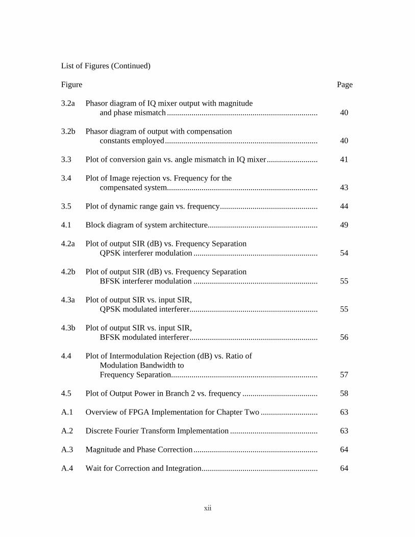
xii
List of Figures (Continued) Figure Page 3.2a Phasor diagram of IQ mixer output with magnitude and phase mismatch .......................................................................... 40 3.2b Phasor diagram of output with compensation constants employed........................................................................... 40 3.3 Plot of conversion gain vs. angle mismatch in IQ mixer......................... 41 3.4 Plot of Image rejection vs. Frequency for the compensated system.......................................................................... 43 3.5 Plot of dynamic range gain vs. frequency................................................ 44 4.1 Block diagram of system architecture...................................................... 49 4.2a Plot of output SIR (dB) vs. Frequency Separation QPSK interferer modulation ............................................................. 54 4.2b Plot of output SIR (dB) vs. Frequency Separation BFSK interferer modulation ............................................................. 55 4.3a Plot of output SIR vs. input SIR, QPSK modulated interferer............................................................... 55 4.3b Plot of output SIR vs. input SIR, BFSK modulated interferer............................................................... 56 4.4 Plot of Intermodulation Rejection (dB) vs. Ratio of Modulation Bandwidth to Frequency Separation........................................................................ 57 4.5 Plot of Output Power in Branch 2 vs. frequency ..................................... 58 A.1 Overview of FPGA Implementation for Chapter Two ............................ 63 A.2 Discrete Fourier Transform Implementation ........................................... 63 A.3 Magnitude and Phase Correction ............................................................. 64 A.4 Wait for Correction and Integration......................................................... 64

xiii
List of Figures (Continued) Figure Page A.5 IF Upconversion....................................................................................... 65 A.6 Summation of initial and corrected signals.............................................. 65 A.7 FPGA Implementation for Chapter Three ............................................... 66 A.8 DSP Implementation for Chapter Three .................................................. 67 A.9 FPGA Implementation for Chapter Four ................................................. 68 A.10 QPSK Modulation.................................................................................... 68 A.11 64-QAM Modulation ............................................................................... 69 A.12 BPSK Modulation.................................................................................... 69 A.13 BFSK Modulation.................................................................................... 70 A.14 IF Upconversion....................................................................................... 70 A.15 Amplitude Set .......................................................................................... 71

1
PREFACE
This preface introduces to the reader the context, scope and significance of the
work contained in this dissertation. The context in which this dissertation is introduced is
the advent of software defined radio (SDR), which has fundamentally altered wireless
communication system design. Before SDR, the only part of the transmitter design that
was digital was the bit stream used to modulate a radio frequency carrier. The
modulation, pulse shaping, frequency upconversion, filtering, and amplification were all
performed in hardware. Now portions of each of these five tasks can be performed in
software. Because many of the tasks are implemented in software, there is a great deal of
latitude to be offered in an SDR as opposed to its traditional counterparts. For example,
implementation of multiple modulation schemes and pulse shapes exhibits greater
flexibility, as well as economy, when performed in software rather than hardware. This
flexibility enables the emerging technology of cognitive radio in which communicating
radios adapt to their radio frequency environment to optimize communication
performance. Adaptation in frequency of operation is particularly valuable in taking
advantage of otherwise unused portions of the spectrum.
As a consequence of the change of technology, radio design has become a
multidisciplinary activity. Designers of radio hardware must now allow a digital signal
processing (DSP) engineer to take on much of the design that was previously done in
hardware, and design the remaining hardware in a way that will integrate seamlessly with
the digital design. The DSP engineer must also understand the process of the full radio

2
system to be able to compensate for the strengths and weaknesses inherent in the analog
hardware design.
In scope this dissertation analyzes and integrates the hardware and software side
of an SDR for optimum radio frequency performance. In the first paper, a device is
introduced that is able to give baseband feedback of radio frequency properties suitable
for analysis in software. In the three subsequent papers, three applications for the device
are devised. The first is an image rejection upconverter that achieves greater than 65 dB
of image rejection over a broad frequency range without the use of a radio frequency
filter. The second application is a baseband correction scheme for extending the
bandwidth and improving the magnitude and phase accuracy of an off-the-shelf IQ mixer.
The third application is a receiving scheme that rejects a near-band, high-power interferer
again without the use of a radio frequency filter. For each of the four papers, both
theoretical development and experimental verification are performed.
It is this paradigm of integrating software feedback and baseband compensation in
order to improve radio frequency performance that defines the significance of this work.
Previously, the designer of radio frequency circuits would simply try to optimize the RF
performance of a particular device that would then have to interact with only adjacent
components, possibly incorporating a switched system for increased frequency or
amplitude range such as that implemented by Tiiliharju in [P.1]. In the same vein,
Gruszczynski et. al designed an analog compensation structure to obviate directly the
parasitics that cause the performance degradation of RF devices in [P.2]. While his work
achieves significantly improved RF performance, it pays the price of complexity, number

3
of components, and a lack of ability to adjust parameters in real time. A real time solution
to RF impairments was implemented by Vasudev and Collins in [P.3], in which they
employed feedback through a square law detector to solve the problem of image
rejection. However, their experimental setup employed benchtop instruments, which also
adds an unnecessary layer of complexity and more dynamic range than is necessary. They
also did not envision the application of this concept to the compensation of other radio
frequency impairments.
This dissertation introduces a robust baseband feed and control network to
compensate for non-ideal performance in RF and microwave circuits. Through subjecting
these RF devices to a closed-loop system, it extends the work of Vasudev and Collins. RF
performance such as image rejection, interference rejection, and bandwidth are greatly
improved with the application of simple signal processing techniques that account for
certain non-ideal behaviors in the hardware that limit performance. In this work,
commercial off-the shelf components and programmable logic components are employed
to yield SDR functionality that extends the state of the art in radio frequency performance
through intelligent integration of the hardware and software.
References
[P.1] E. Tiiliharju “Integration of Broadband Direct-Conversion Quadrature Modulators,” PhD. Dissertation, Dept. Elect. Eng., Helsinki Univ. of Tech., Helsinki, Finland, 2006.
[P.2] S. Gruszczynski, K. Wincza, and K. Sachse, “Design of Compensated Coupled-Stripline 3-dB Directional Couplers, Phase Shifters, and Magic-T’s—Part I: Single-Section Coupled-Line Circuits,” IEEE Trans. Microwave Theory and Tech., Vol. 54, no. 11, November, 2006, pp. 3986-3994

4
[P.3] N. Vasudev and O. M. Collins, “Near ideal RF Up converters,” IEEE Trans. Microwave Theory Tech. vol. 50 pp. 2569-2575, Nov 2002

5
MULTITONE FEEDBACK THROUGH A DEMODULATING LOG DETECTOR FOR DETECTION OF SPURIOUS EMISSIONS IN SOFTWARE RADIO
Abstract— This paper provides an analysis of a log detector in order to determine
its response to a multi-tone input for detection of spurious emissions in a radio
frequency transmitter. Treatment is given to the single tone response of the log
detector and extended to a two-tone log detector system, where a large signal and a
small signal are present. The large signal is observed to experience logarithmic
processing with an output at zero frequency. The small signal produces an output at
the difference frequency of the large signal frequency and small signal frequency
that is approximately proportional to the ratio of the small signal voltage to the
large signal voltage. The two-tone results are generalized to an m-tone input.
Experimental results are presented to show the accuracy of the model. The log
detector circuit analyzed is able to detect a spurious emission within 45 MHz of the
main signal with + 1 dB of accuracy.
I. Introduction
Since the advent of software defined radio (SDR), it has been seen as an attractive
possibility to apply all radio functionality in software, employing solely a digital-to-
analog and analog-to-digital conversion stage and an antenna for hardware functionality
and thereby bypassing the need for radio frequency hardware [1.1]. Because of the cost
and complexity inherent in the data conversion stage for such a system, current software
defined radios seem to be settling for the data conversion at baseband or a low
intermediate frequency and relying on traditional radio frequency hardware to perform

6
the high frequency amplification, filtering, and frequency conversion functions [1.2].
RF hardware is unattractive in many cases because of spurious emissions
produced in the frequency conversion and amplification stages. Traditionally, these
problems have been solved by radio frequency (RF) filters. It is desirable, however, to
have a dynamic radio that may function over a variety of frequency bands. For this type
of radio, a traditional RF filter is replaced by a more costly and complex frequency-agile
filter.
An alternative to the frequency-agile filter is to provide digital feedback to the
software component of the radio that allows for cancellation of the spurious emissions.
Vasudev and Collins [1.3] suggest that a square law detector be used to provide software
feedback of spurious emissions caused by local oscillator leakage and unrejected images
of the desired RF signal. The square law detector is unattractive because of the wide
dynamic range required to process the feedback signal.
A logarithmic (log) detector is studied in this paper as a means for providing this
kind of feedback. The theoretical output of a log detector is given by
( ) ( )( )2log ( )out inv t C LPF v t= (1.1)
Where C is a constant determined by the log detector and LPF denotes the low-
pass filter function. When the input comprises two sinusoidal tones, the output is given
by
( ) ( ) ( )2
2 1 10
0 0
1log log cos2out
V Vv t C V tV V
ω φ⎡ ⎤⎛ ⎞⎛ ⎞ ⎛ ⎞⎢ ⎥⎜ ⎟⎜ ⎟ ⎜ ⎟⎜ ⎟ ⎜ ⎟⎢ ⎥⎜ ⎟⎝ ⎠ ⎝ ⎠⎢ ⎥⎝ ⎠⎣ ⎦
= + + + Δ + Δ (1.2)
Where V0 is the amplitude of the first sinusoid and V1 is the amplitude of the

7
second. ωΔ and φΔ are the radian frequency and phase differences, respectively. With
the assumption that the ratio of V1 to V0 is very small, we may use the first order Taylor
approximation to the log(1/2 +x) to get
( ) ( )2
0 1
0log 2 cos
2outV Vv t C t
Vω φ
⎡ ⎤⎛ ⎞ ⎛ ⎞⎢ ⎥⎜ ⎟ ⎜ ⎟⎜ ⎟⎜ ⎟⎢ ⎥⎝ ⎠⎝ ⎠⎣ ⎦
≈ + Δ + Δ (1.3)
This expression is attractive because it allows for separation of the small-tone
signal by use of the discrete Fourier Transform (DFT), and its output at the difference
frequency is proportional to the ratio of the spurious tone to the main tone. It is this ratio
that is to be minimized for optimal performance. The feedback proportional to the ratio
would give information to the software on this performance with a dynamic range
requirement proportional to the desired spurious-free-dynamic-range improvement, rather
than the total dynamic range required. There is a question, however, as to whether current
log detector circuits will in fact exhibit this behavior since they are designed to merely
approximate the logarithmic response. In the literature currently, there is no treatment of
the multi-tone response of a log detector.
Fig. 1.1. Block Diagram of Analog Devices AD8318 Log detector [1.2]. The response of this logarithmic amplifier configuration is analyzed for multi-tone inputs.

8
We have implemented a multi-tone feedback scheme, employing an Analog Devices
AD8318 logarithmic amplifier. A treatment of how the one-tone behavior of this
structure approximates a log function is contained in the manufacturer’s application note
for the device [1.4]. The schematic structure of this is given in Figure 1.1. The following
section reviews briefly the single-tone principles of operation of this device, for the sake
of establishing terminology and methodology. Sections III and IV provide extensions to
two and more tones. Experimental results are presented in Section V.
Vin
Vout
actual
ideal
Fig. 1.2. A/0 Voltage characteristic. Notice that for the ideal, the voltage gain is A for the linear region, and 0 elsewhere.
II. Log Detector with Single Tone Input
An ideal logarithmic amplifier produces an output
0logoutref
Vv C V⎛ ⎞⎜ ⎟⎝ ⎠
= (1.4)
where C and Vref are internal parameters of the detector and the input is given by
( ) ( )0 0sininv t V tω= . (1.5)
AEK
EK

9
In spectral analysis later in the paper, the Fourier Transform of (1.4) is required. The
presence of the logarithm in (1.4) precludes even contour integral methods for computing
the needed transform. However, the log detector employs a piecewise-linear
approximation to the log function and the Fourier transform of this approximation is
tractable.
The schematic in Figure 1.1 comprises amplifier cells with piecewise linear gain
response, as shown in Figure 1.2. The cell is a so-called A/0 amplifier because the slope
of the ideal gain curve is A over a linear region extending to Vin= EK, and is zero at
higher voltages. This ideal characteristic is approximated in the log detector by a
hyperbolic tangent function. The piecewise linear characterization is adequate for the
present analysis. For cascaded cells, the hyperbolic tangent approximations converge
quickly to the ideal A/0 behavior as seen in Figure 1.3.
The detector cells shown in Figure 1.1 are full wave rectifiers that perform the
absolute value function followed by a low-pass filter. Each of these detector cells also
has baseband gain that sets the slope of the log detector output, which is the constant C in
equation (1.4). The detector cell output currents are then summed and converted to an
output voltage, which is again low-pass filtered.
A logarithmic amplifier employs a total of K amplifiers. The amplifiers furthest
along the cascade in Figure 1.1 are more strongly saturated, and more amplifiers are
saturated for a higher input level. Specifically, the number of amplifiers operating in the
linear region is

10
0int int log K
AEN RV
⎡ ⎤⎛ ⎞⎡ ⎤ ⎢ ⎥⎜ ⎟⎣ ⎦ ⎜ ⎟⎢ ⎥⎝ ⎠⎣ ⎦
= = (1.6)
and R is the logarithmic ratio of the knee voltage in Fig. 2 to the maximum input voltage
For the Nth amplifier in the cascade, the input is AN-1 times vin(t). The input to their
respective detector cells will simply be the input voltage multiplied by AN. For
subsequent amplifiers, there will be compression in the output of the amplifier due to the
characteristic A/0 shown in Figure 1.2. In the saturated region, the amplifier cell clips the
output of the sinusoid.
Anticipating the need for a Fourier transformable form, we construct the
expression for the voltage output of amplifier k where k>N and have
( ) ( )
0
0
0,
04
04
2
1 4
1 ,4
sat
sat
sat
kin Tamp k
q
K T T
K T T
qTv t A v t p t
AE p t q T
AE p t q T
∞
=−∞
−
−
⎧ ⎛ ⎞⎪⎨ ⎜ ⎟⎪ ⎝ ⎠⎩
⎛ ⎞⎛ ⎞⎜ ⎟⎜ ⎟
⎝ ⎠⎝ ⎠⎫⎛ ⎞⎛ ⎞ ⎪
⎜ ⎟⎬⎜ ⎟⎝ ⎠ ⎪⎝ ⎠⎭
= −
+ − +
− − −
∑
(1.7)
where T0 is the period of νin, Tsat is the time of saturation—the time at which the
amplifier reaches the saturation region—given by
( )1
10
0 0
sin sin,
KR kk
sat
EAA V
Tω ω
−− −
⎛ ⎞⎜ ⎟⎜ ⎟⎝ ⎠= = (1.8)
and the pulse function is defined as
( ) 1, | |.
0, | |Tt T
p tt T
⎧⎨⎩
<=
> (1.9)

11
These expressions are the time-domain representations of the voltages at the input
to each of the K detectors. As stated above, the detector cells perform both the absolute
value and low-pass filtering function on their respective inputs. For the first N+1
detectors, the output before low pass filtering is
( ) ( ) ( )0 00 0,4 4
2 1 2 34 4
k kin inT Trect k
q
q qv t A v t p t T A v t p t T∞
=−∞
⎧ ⎫⎛ ⎞ ⎛ ⎞⎛ ⎞ ⎛ ⎞⎪ ⎪⎜ ⎟ ⎜ ⎟⎨ ⎬⎜ ⎟ ⎜ ⎟
⎝ ⎠ ⎝ ⎠⎪ ⎪⎝ ⎠ ⎝ ⎠⎩ ⎭
− −= − − −∑ (1.10)
for 0 k N≤ ≤ . The expression for k>N is given by
( ) ( ) ( )0 00 0, , ,4 4
2 1 2 3 .4 4T Trect k amp k amp k
q
q qv t v t p t T v t p t T∞
=−∞
⎧ ⎫⎛ ⎞ ⎛ ⎞⎛ ⎞ ⎛ ⎞⎪ ⎪⎜ ⎟ ⎜ ⎟⎨ ⎬⎜ ⎟ ⎜ ⎟
⎝ ⎠ ⎝ ⎠⎪ ⎪⎝ ⎠ ⎝ ⎠⎩ ⎭
− −= − − −∑ (1.11)
Expression (1.11) is Fourier transformed in order to model the low-pass filter function of
the detector in the frequency domain. Because of the periodicity in the time-domain,
each of the transforms is a sum of impulses in the frequency domain. The following
expression results for 0 k N≤ ≤ :
0
0.5
1
1.5
2
2.5
0 2 4 6 8 10
Number of Cascaded Cells
Perc
ent E
rror
Fig. 1.3. Error in A/0 ideal characteristic vs. number of cascaded cells. Notice that the error dampens rather than propagating further through the cascaded cells, allowing us to use the piecewise-linear A/0 formulation for the analysis.

12
( ) ( )( )
( )( )
0
0
00
1 40 0,
00
1 4
sin ( 1) 441
sin ( 1) 4 .
1
m
m
j q Tkrect k
q
j q T
TqV A V q e
j q
Tqe
q
ω
ω
ωπ δ ω ω
ω
∞− −
=−∞
− +
⎧ ⎡ ⎛ ⎞⎪ ⎜ ⎟⎢⎪ ⎝ ⎠⎢⎨
⎢⎪⎢⎪ ⎣⎩
⎫⎤⎛ ⎞⎪⎜ ⎟ ⎥⎪⎝ ⎠ ⎥⎬
⎥⎪⎥⎪⎦⎭
−= −
−
+−
+
∑ i
(1.12)
Similarly, for k>N,
( ) ( )( ) ( )
( )( ) ( )
0
0
20
1 20 0,
20
1 2
sin ( 1)24 1
1
sin ( 1)2 1
1
4
m
m
sat
j q Tkrect k
q
sat
j q T
TqV A V q e
q
Tqe
q
j
ω
ω
ωπ δ ω ω
ω
π
∞− −
=−∞
− +
⎧ ⎡ ⎛ ⎞⎪ ⎢ ⎜ ⎟⎪ ⎝ ⎠⎢⎨ ⎢⎪ ⎢⎪ ⎣⎩
⎫⎤⎛ ⎞⎪⎥⎜ ⎟ ⎪⎝ ⎠ ⎥⎬⎥⎪⎥⎪⎦⎭
−= − −
−
+− −
+
+
∑
( )
( )( ) 0
0
1 40 0
2sin
22 .m
sat
j q TR
q
T Tq
A V q eq
ω
ωδ ω ω
∞− −
=−∞
⎧ ⎫⎛ ⎞⎪ ⎪⎜ ⎟
⎜ ⎟⎪ ⎪⎪ ⎪⎝ ⎠⎨ ⎬⎪ ⎪⎪ ⎪⎪ ⎪⎩ ⎭
−
−∑
(1.13)
The low-pass filter in the detector attenuates all components except for q = 0. By
substitution, the output of detector k is found to be
( ) ( )0det
det, 20 0 0 0det
8 ,
4 4 sin 2 ,2
k
k k Rsatsat
A G V k NV TG V A A T T k N
πδ ω
π ω ω
⎧⎪
⎡ ⎤⎨ ⎛ ⎞⎢ ⎥⎜ ⎟⎪
⎝ ⎠⎣ ⎦⎩
− ≤=
− + − >i (1.14)
where Gdet represents the gain of each detector. The final output of the log detector is
simply the sum of each of the detector outputs, given by
det,0
,K
out kk
V V=
= ∑ (1.15)

13
where K+1 is the total number of detectors. Figure 1.4 shows a plot of Vout and the log of
the magnitude of the input signal, with a value of Gdet that gives the best fit. The multi-
tone input may be analyzed utilizing this single-tone result with the small signal
assumption for tones not residing at ω0.
0
0.5
1
1.5
2
2.5
-60 -40 -20 0
Pin (dBm)
Log
Det
ecto
r Out
(V a
t DC
) idealcalculated
Fig. 1.4. Output Voltage vs. Input Power for Single Tone Input. The deviation from the ideal is less than 2 dB.
III. Two-Tone Response
The two-tone response of the log detector may be analyzed similarly. The input
signal is given as
( ) ( ) ( )0 0 1 1 1sin sininv t V t V tω ω φ= + + (1.16)
with the assumptions that
0 1V V , (1.17)
and
0 1| | 2 Bω ω π− < , (1.18)

14
where B is the corner frequency of the low pass filter at the output of the detector cell,
which is 45 MHz for the device analyzed. Because of (1.17), it is inferred that the
nonlinear behavior of the amplifiers is exactly the same as in the single tone analysis,
meaning that R, N, and Tsat remain unchanged. In fact, all of the time domain
expressions are valid with the simple substitution of (1.16).
The Fourier transforms are a bit more involved because of nonlinear effects in the
log detector. The following expression is added to (1.12) for 0 k N≤ ≤ :
( ) ( )( )
( ) ( )( )
0 0
0 0
00
1 41 0 1, 1
00
1 41 0 1
sin ( 1) 44 ( 1)1
sin ( 1) 44 ( 1)1
j q Tkrect k
q
j q Tk
TqV A V q e
j q
TqA V q e
j q
ω
ω
ωπ δ ω ω ω
ωπ δ ω ω ω
∞− +
=−∞
− −
⎧ ⎛ ⎞⎜ ⎟⎪⎪ ⎝ ⎠
⎨⎪⎪⎩
⎫⎛ ⎞⎜ ⎟ ⎪⎪⎝ ⎠
⎬⎪⎪⎭
+= − − −
+
−− − + +
−
∑ i
i
. (1.19)
The corresponding term to be added to (1.13) is
( )( ) ( )( ) ( )
( ) ( )( ) ( )
0 0
0 0
20
1 21 0 1, 1
20
1 21 0 1
sin ( 1)24 1 1
1
sin ( 1)2 4 ( 1) 1 .
1
sat
j q Tkrect k
q
sat
j q Tk
TqV A V q e
q
TqA V q e
q
ω
ω
ωπ δ ω ω ω
ωπ δ ω ω ω
∞− +
=−∞
− −
⎧ ⎛ ⎞⎪ ⎜ ⎟⎪ ⎝ ⎠⎨⎪⎪⎩
⎫⎛ ⎞⎪⎜ ⎟⎪⎝ ⎠⎬⎪⎪⎭
+= − − − −
+
−− − + + −
−
∑ i
i
(1.20)
The output has additional spectral components at the difference frequencies of ω0 and ω1
due to intermodulation resulting from non-linearity. The filtered output is given by (1.14)
summed with the following term that is the q=0 value of (1.19) and (1.20).

15
( )( )
( )( )
0 11det
0 1det, 1
0 121 0det
0 1
4 ,
.
8 sin ,2
k
k
k sat
A G V k N
VTA G V k N
δ ω ω ωπ
δ ω ω ω
δ ω ω ωπ ω
δ ω ω ω
⎧ ⎛ ⎞⎪ ⎜ ⎟⎪ ⎜ ⎟⎪ ⎝ ⎠⎨
⎛ ⎞⎪ ⎛ ⎞ ⎜ ⎟⎪ ⎜ ⎟ ⎜ ⎟⎝ ⎠⎪ ⎝ ⎠⎩
+ −≤
+ − +=
+ −>
+ − +
i
i
(1.21)
Application of (1.15) with the summand being (1.14) plus (1.21) gives the complete
response to two tones. The addition of (1.21) to account for the presence of the second
tone introduces the intermodulation products present in (1.21) along with the fundamental
present in (1.14). The individual spectral components can be separated in hardware
through digital filtering.
The signals are now separated in order to find the response of the log detector at
these difference frequencies. It is clear from (1.20) and (1.21) that the result at the
difference frequency is linear with respect to the small quantity V1. The influence of V0 is
implicit, since it is V0 that defines the terms Tsat and N found in (1.21). (These parameters
define the analog logarithmic approximation of the entire circuit.)
We first simplify (1.21) for k>N. In order to accomplish this, we substitute Tsat
from (1.8), with the result
( ) ( )( )
10 12
1det, 1 det0 1
sin8 sin , .
2
R kk
k
AV A G V k N
δ ω ω ωπ
δ ω ω ω
− −⎛ ⎞ ⎛ ⎞⎜ ⎟ ⎜ ⎟⎜ ⎟ ⎜ ⎟
⎝ ⎠⎝ ⎠
+ −= >
+ − +i (1.22)
Under the condition that AR-k is small, the small-argument approximation to the sine is
applicable and we are left with
( ) ( )21 0 1 0 1det, 1 det2 , .R k
kV G A V k Nπ δ ω ω ω δ ω ω ω− ⎡ ⎤⎣ ⎦≈ + − + − + >i (1.23)

16
With this result, we can identify the output sum due to the small-signal tone into two
series to form an expression for the small signal output given by
( )( ) 21 1 0 1det
0 12 2 .
N Kk R k
outk k N
V G V A A Aπ δ ω ω ω −
= = +
⎛ ⎞⎜ ⎟⎝ ⎠
≈ − +∑ ∑∓ i (1.24)
The sums of two geometric series of A are contained in (1.24), and can be replaced with
their closed forms giving
( )( )( )( )1
1 1 0 1det
2 2 12 .
1
N R R R N N KR
out
A A A AV G A V
Aπ δ ω ω ω
− + − − −− + −= −
−∓ i (1.25)
If V0 is small enough such that 0 1,RKA V E− = and also if V0 is sufficiently large such that
1N KA − --i.e., that some amplifiers are saturated, we are left with an expression for the
output at the difference frequency of the form
( )( ) ( )11
1 0 1det0
22 .
1
N R R N
Kout
A AVV G EV A
π δ ω ω ω− + −+
≈ −−
∓ i (1.26)
In (1.26), use is made that 0R
KA E V= to eliminate the explicit appearance of AR.
One can see that the output at the difference frequency is proportional to the ratio
of V1 to V0. A plot of this expression along with a plot of the exact expression is given in
Figure 1.5 for a constant ratio of V1 /V0. The approximation (1.26) fails near the upper
end of the operating range. The periodic behavior in this figure is due to the AR-N term in
the expression. Since N is the greatest integer less than R, each period denotes R crossing
an integer value.

17
-55-53-51-49-47-45-43-41-39-37-35
-60 -50 -40 -30 -20 -10 0
Main Lobe Power (dBm)
Log
Det
ecto
r Out
(dB
m a
t f1-
f 0)
exact
approximate
Fig. 1.5. Power out at difference frequency vs. power in the main lobe. For this plot, the ratio of the power in the large tone and small tone was held constant while the total power was scaled. As can be seen, the approximate analysis breaks down at power levels that violate the assumptions made.
IV. M-tone Input
We may adopt all of the analysis of the previous section as also valid for an input
at ωm in a multitone system provided
0 11
,M
mV V
=∑ (1.27)
and
0| | 2m Bω ω π− < . (1.28)
Then for a sampled signal
( ) ( ) ( )0 01
sin sinM
in m m mm
v t V t V tω ω φ=
= + +∑ , (1.29)
we have the response
( )( ) ( )1
, det 00
22 .
1
N R R Nm
out m K m
A AVV G E
V Aπ δ ω ω ω
− + −+≈ −
−∓ (1.30)

18
If in the set of tones in (1.29), two frequencies are separated upward and downward from
ω0 by the same amount, they are aliased together and cannot be separately identified.
This is described mathematically as follows
0 0| | | |m iω ω ω ω− ≠ − . (1.31)
V. Experimental Verification
The experimental configuration for the verification of the two-tone derivation is
given in Figure 1.6. The two synthesizers used were identical Agilent E4433B Signal
Generators labeled A and B operating at 2.4 GHz and 2.4005 GHz respectively. The
hybrid used to sum the signals is a Narda 4346 hybrid, and the spectrum analyzer used to
deduce the power levels at the input and output is the HP 8565E. It is the NIST traceable
calibration on this spectrum analyzer that provides the power reference for the
measurements.
Linearity was first evaluated The power level of signal generator A was set to -17
dBm at the input to the log detector, and signal generator B varied its power level over an
80 dB range, leaving the results shown in Figure 1.7. This figure shows the linearity of
the log detector response to be within 1 dB over 75 dB of dynamic range.

19
Synth Af=2400 MHz
RF
Synth Bf=2400.5MHz
RF
SpectrumAnalyzer
RFO
C
I
DUT=AD 8318Log det
Fig. 1.6. Experimental Configuration. This experimental setup was designed to test the accuracy of the computed results.
The second test performed was the verification of the results shown in Figure 1.5.
For this test the power level of signal generator A was set to be 40 dB below that of
signal generator B, and the power level of each was varied over a >55 dB range. Figure
1.8 shows the experimental output and the calculated output from (1.25). The factor Gdet
in (1.25) is not explicitly available, and the two curves in the figure have been visually
aligned. The calculated results manifest abrupt transitions at the knees of individual
amplifier responses. In contrast, the experimental results demonstrate a smoother
approximation to the desired behavior in (1.3) by being constant within 1 dB over a 40
dB range of input power with the ratio of main lobe to side lobe power held constant.
The results of Figure 1.7 and Figure 1.8 together demonstrate that over a 40 dB
range of main lobe power, the ratio of main lobe to side lobe power ranging from 5 to 80
dB relative to main lobe power can be determined to within 2 dB.

20
-90
-70
-50
-30
-10
10
-100 -80 -60 -40 -20 0
Side Lobe Power (dBm)
Log
Det
ecto
r Out
(dB
m a
t f0
- f1)
Fig. 1.7. Experimental Power out at difference frequency vs. Power in at f1 For this plot, the large tone power was held constant at -17 dBm while the sidelobe power was scaled. As can be seen, the output is linear within 1 dB over a 75 dB range.
VI. Conclusions
A logarithmic detector is designed to logarithmically scale a single RF input and
convert it to baseband. When such a detector is operated with small sideband signals, it is
found to convert these signals to sidebands at their difference frequencies from the
-55-53-51-49-47-45-43-41-39-37-35
-60 -40 -20 0
Main Lobe Power (dBm)
Log
Det
ecto
r Out
(dB
m a
t f1 -
f 0)
calculatedmeasured
Fig. 8. Power out at difference frequency vs. power in the main lobe. For this plot, the ratio of the power in the large tone and small tone was held constant while the total power was scaled. The error between the calculated and measured responses is caused by inaccuracies in the piecewise linear approximation of the amplifier cell response.

21
principal RF carrier. The phasor representations of these signals are not logarithmically
scaled, but rather are proportional to the ratio of the sideband voltage to the RF voltage,
1 0V V .
Because this is a phasor ratio, the phase correspondence principal holds for the
phase differences. Further, the magnitude of the sideband responses is scaled and only the
relative amplitudes in the collection of signals into the amplifier affect the output.
Changing input levels for the entire collection of signals are buffered by this scaling.
Experimental evaluation of the process and model described here showed linearity
of a low level signal relative to the principal RF signal within ±1 dB. The logarithmic
response for the principal signal showed deviation between the piecewise linear model
and the measured response as high as 3 dB. This difference is due to the error in the
piecewise approximation of the hyperbolic tangent.
References
[1.1] J. Mitola, “The Software Radio Architecture,” IEEE Commun. Mag., vol. 33, no. 5, May 1995, pp. 26–38.
[1.2] P.B. Kennington, RF and Baseband Techniques for Software Defined Radio. pp. 199-200, Artech House, 2005.
[1.3] N. Vasudev and O. M. Collins, “Near ideal RF Up converters,” IEEE Trans. Microwave Theory Tech. vol. 50 pp. 2569-2575, Nov 2002
[1.4] “AD8307 Data Sheet” Analog Devices Inc., Norwood, MA, 2003, pp.7-10.

22
FREQUENCY AND AMPLITUDE AGILE IMAGE REJECTION USING A LOG DETECTOR FEEDBACK SYSTEM
Abstract— In the context of dynamic spectrum utilization, it is attractive to
possess a single-sideband transmitter that is frequency-agile while maintaining the
low out-of-band emissions of its fixed-band counterparts without the use of a
frequency-agile RF band pass filter. This paper introduces a frequency- and
amplitude-agile image rejection scheme based on a feedback loop through a
broadband log detector. Implementation is performed with an off-the-shelf
upconverter and log detector. Compensation is performed digitally in a software-
defined-radio platform, as shown in Figure 2.1. The log detector feedback loop
requires dynamic range on the order of the desired image rejection improvement,
rather than a previously-devised system that requires a dynamic range on the order
of the total image rejection. The analog to digital conversion (ADC) in the feedback
loop processes a signal at twice the intermediate frequency to sense the present level
of rejection, and this result is employed in software to suppress the undesired image.
Image rejection of greater than 65 dB is demonstrated over the 802.11A and
802.11G frequency bands using an off-the-shelf upconverter. The system maintains
greater than 65 dB of image rejection when the power level is adjusted over a 30 dB
range. Linear feedback control analysis is performed to obtain figures of merit for
the stability and fall-time properties of the feedback system. Performance
degradation due to inaccuracies in the feedback compensation over the frequency
range of the system is analyzed. This feedback-image-rejection scheme allows an off-

23
the-shelf upconverter to maintain a low out-of-band emission level over its entire
frequency and amplitude range without the use of a radio frequency band pass
filter.
I. Introduction
In software-defined and frequency-agile radio development, it is attractive to have
a frequency-agile transmitter that possesses similar performance to its traditional fixed-
band counterparts. A major obstacle to this goal is image rejection, which is generally
performed at the radio frequency (RF) with an analog RF filter. For a frequency-agile
transmitter, the RF frequency is not fixed, however, and an analog image-reject filter
would also have to be frequency-agile, with concomitant complexity and cost.
Schemes have been proposed for image rejection with mixed results. One method
that gained momentum in the nineties was the image-rejection mixer [2.1]. This mixer
cancels the negative image using complex arithmetic in digital processing to affect a 90-
degree phase shift in the unwanted image. An additional 90-degree phase shift at the in-
phase/quadrature (IQ) mixer completes a 180-degree phase shift for cancellation. While
this method is highly attractive, its rejection properties are dependent on a tightly
controlled magnitude and phase match in the 2 channels of an IQ mixer. A phase match
of within half of a degree is required to achieve an image rejection of 60 dB [2.2]. Such a
phase match is unrealistic in the face of changing frequency in a frequency-agile system.
Vasudev and Collins [2.3] proposed a method of using feedback through a square
law detector for image cancellation, though not in the context of frequency agility. They
were able to improve the image rejection of an off-the-shelf upconverter by more than 20

24
dB using feedback through a spectrum analyzer. The dynamic range that a spectrum
analyzer provides is not directly achievable in a manufactured transmitter, and the
feedback scheme must be augmented in order to sense the image signal and reject it.
Although it provides valuable proof-of-principle for the use of digital feedback in RF
systems, linear feedback control analysis of the system is not performed. Further work is
required to implement this system in a practical transmitter.
In [2.4], a log detector is analyzed for its multi-tone response and it is established
that the voltage at the difference frequency is proportional to the ratio between two
voltages: that at the image frequency and that at the main lobe. The results in [2.4]
demonstrate that a measurement of the voltage at the difference frequency will yield a
value proportional to this ratio within 2 dB of the actual ratio. To employ this ratio as
feedback to digital processing, an analog to digital converter (ADC) with a dynamic
range on the order of the desired rejection improvement is required, along with fixed
amplification to raise the signal at the difference frequency to a level compatible with the
ADC.
The present paper demonstrates frequency- and amplitude-agile image rejection
utilizing linear feedback control through a log detector and board-level processing
devices to achieve the required image rejection. An overview of the system and its
components is given in Section II. Linear feedback control analysis for the system is
given in Section III. Experimental Results are given in Section IV.

25
LogDetectorAD8318
Narda 4227-16Cpl= 16.0 dB
OI
C
SpectrumAnalyzer
RFGPIB
IL= 1.00 dBFCO= 15.00 MHz
Minicircuits LPF
LyrtechSignalMaster
TMS320C6701 / Virtex-II
ADC DAC DAC Maxim 2828Upconverter
I RF
Q
Figure 2.1. Block diagram of feedback system. The Lyrtech board comprises an FPGA, a DSP processor, and two channels each of ADC and DAC.
II. System Description
The experimental configuration for the feedback-image-rejection scheme is given
in Figure 2.1. The Xilinx Virtex FPGA embedded in a Lyrtech SignalMaster®
Development Platform generates in-phase and quadrature (I and Q) sinusoids at an
intermediate frequency (IF) that are conditioned for image rejection as described above
and in [2.1]. These IF signals are then upconverted and amplified by the Maxim® 2828
upconverter. That signal is then sampled by the Narda® 4227 coupler, with the main
signal going to the spectrum analyzer for observation and the component that is 16 dB
down going to the Analog Devices® AD8318 log detector. The output of the log detector
is then amplified, low-pass filtered, and fed back into the Development Platform to be
processed and added to the transmit channel to cancel the unwanted image. The output is
monitored with a spectrum analyzer for evaluation of the scheme.
The processing performed by the FPGA is shown in Figure 2.2 as a Matlab
Simulink® block diagram used to program the Development Platform. The FPGA

26
employs the value of the Discrete Fourier Transform (DFT) at the difference frequency as
a feedback value proportional to the voltage ratio of the image to the main lobe. This
feedback is integrated over time, then its magnitude is scaled and its phase is shifted to
give negative feedback. This conditioned feedback signal is then upconverted to the
negative intermediate frequency, added to the original signal, and sent to the digital-to-
analog converters, producing the I and Q output channels. The feedback continues until
the noise floor is reached either in the feedback system or the transmitter.
The noise floor of the feedback is set in part by the DFT implementation. In this
particular example, a 768-point DFT was used. The DFT is not performed continuously.
A time delay allows feedback effects to establish before starting the next DFT cycle,
allowing the transients associated with the feedback to decay prior to taking the next
DFT. The FPGA was programmed using the Xilinx System Generator Plug-in for
Simulink as well as the Lyrtech FPGALink Plug-in. The FPGA does not compensate for
changes in the RF frequency or power levels. The compensation occurs solely through
the feedback loop.
The feedback scaling constant was determined first by experimental data on the
log detector from [2.4] and then fine-tuned experimentally in the configuration of Figure
2.1. The feedback phase offset was determined in a similar manner. The desired
theoretical value and the effect of errors in the complex feedback constant, K , are
analyzed in Section III. Based on the capability of the log detector, the feedback system
is functional between 1 MHz and 8 GHz. The Maxim upconverter operates in frequency

27
ranges allocated for 802.11A and 802.11G (4.9-5.9 GHz and 2.4-2.5 GHz, respectively).
Thus the upconverter limits the frequency agility of the overall system.
Figure 2.2. Simulink Block Diagram of feedback processing performed in the FPGA.
III. Linear Feedback Control Analysis
The system described above may be analyzed as a linear feedback control system.
This yields quantitative results for both the stability and transient behavior of the system.
A block diagram of the control system model is given in Figure 2.3. The system is
modeled as discrete-time because changes to the image rejection occur only at times that
the DFT output changes. The z transform is therefore used to analyze the system, as is
shown in the block diagram. The resulting transfer function is
( ) ( )1 , 1
1zH z z AK
z AK−= > −
+ −. (2.1)
A is a phasor constant applied by the analog feedback network; K is a phasor
constant applied in software. If the input to the system is the unit step function,

28
representing an image that is initially unrejected, the sample domain response to this
input is found to be
( )1n
y n AK u n⎡ ⎤ ⎡ ⎤⎣ ⎦ ⎣ ⎦= − . (2.2)
Figure 2.3. z domain model for image-rejection system, used for linear feedback control analysis. The conversion block with unit delay represents an ideal zero-order hold which occurs during the combination of the analog to digital conversion and DFT operation.
Equation (2.2) shows that both the fall time and stability of the feedback scheme
depend on the magnitude of the complex expression, ( )1 AK− . The stability condition
requires that
1 1AK − < . (2.3)
Writing AjA Ae φ= and KjK Ke φ= , we deduce the stability condition from (2.3):
( )2 2 2 cos 0KAA K AK φ φ− + < . (2.4)

29
Figure 2.4 displays the constraint (2.4) graphically. The magnitude of the product AK is
displayed as a function of φA+φK. All values of the product lying under the curve yield a
steady-state value of zero for the rejected image. All values above the curve leave the
system unstable.
0
0.5
1
1.5
2
2.5
-90 -60 -30 0 30 60 90
φA+φK
AK
Figure 2.4. Stability Region for Log Detector Feedback Scheme. Values under the curve yield a steady-state value of zero for the rejected image.
Equation (2.2) shows that optimum fall time occurs when 1AK = . The value of A
is set by the analog feedback network and frequency dependence is intrinsic the coupler
and log detector shown in Figure 2.1. The value of K is ideally selected to be the
reciprocal of A . The selected value of K , however, is set by a measurement of
magnitude and phase with accuracy limitations. For the sake of saving memory, it is
attractive for K to be independent of the frequency of operation. It is therefore necessary
to analyze the consequences of a value of K that is not the exact reciprocal of A . If we
employ the 40 dB fall time1 as a figure of merit, we obtain from (2.2)
1 The 40 dB fall time, defined as the smallest value of n for which [ ] .01 [0]y n y< • , for all n>n40.

30
( )( )( )40 2 2
2log .01log 1 2 cos KA
nA K AK φ φ
⎡ ⎤⎢ ⎥⎢ ⎥⎢ ⎥
=+ − +
. (2.5)
Figure 2.5 displays constant-fall-time contours on the stability chart of Figure 2.4.
Complex values inside the enclosed region will result in fall times less than or equal to
the respective value of n40. The optimum (zero) fall time occurs at the point (0,1), lying at
the center of the graph.
0
0.5
1
1.5
2
2.5
-90 -60 -30 0 30 60 90
φ A+φ K
AK
n40=infn40=100n40=20n40=10n40=5
Figure 2.5. Fall Time Regions for Log Detector Feedback Scheme. Values enclosed will result in a 40 dB fall time less than or equal to the associated value of n40.
IV. Experimental Results
The system in Figure 2.1 was exercised as described in Section II. The
intermediate frequency was set to 1 MHz. The software feedback constant, K, for the
system was 5x10⁻⁴, and the feedback phase shift was 90 degrees. The feedback constant
was chosen based on measurements of A and the stability constraint over the desired
frequency range. In the configuration of Figure 2.1, the image-rejection mixing alone
achieved 35 dB of rejection. Figure 2.6 shows the results of feedback-image-rejection vs.

31
frequency. It should be noted that 100 time averages of the spectral data were needed in
the spectrum analyzer in order even to sense the rejected image. Figure 2.6 shows an
image rejection greater than 65 dB over the entire frequency range of the Maxim
upconverter.
Figure 2.7 shows the image rejection at a local oscillator frequency of 2.437 GHz
as a function of the main lobe output power level. The Maxim upconverter contains a
variable gain amplifier (VGA) that can be adjusted over a 30 dB range. This figure
demonstrates the ability of this particular feedback scheme to reject the image over a
broad range of output power levels. One also notes from this figure that the image
rejection is at a higher level at higher power levels up to -10 dBm of transmit power.
65
67
69
71
73
75
77
2.41 2.42 2.43 2.44 2.45 2.46 2.47
Frequency (GHz)
Imag
e R
ejec
tion
(dB
)
Figure 2.6a. Image rejection vs. frequency for 802.11G frequency band.

32
65
67
69
71
73
75
77
4.9 5.1 5.3 5.5 5.7 5.9
Frequency (GHz)
Imag
e R
ejec
tion
(dB
)
Figure 2.6b. Image rejection vs. frequency for 802.11A frequency band.
65
67
69
71
73
75
77
-25 -20 -15 -10 -5 0 5 10
Main Lobe Power (dBm)
Imag
e R
ejec
tion
(dB
)
Figure 2.7. Image rejection vs. main lobe power for a local oscillator frequency of 2.437 GHz.
V. Conclusions and Future Work
The image rejection scheme presented in this paper has been demonstrated to
work over a broad range of frequencies and output power levels with image rejection

33
greater than 65 dB over the bands tested. Further work is required to verify its
effectiveness over other frequency ranges.
References
[2.1] D.K. Weaver, "A third method of generation and detection of singlesideband signals," Proc. IRE, vol. 44, Dec., 1956, pp. 1703-5.
[2.2] L. E. Larson, “Radio Frequency Integrated Circuit Technology for Low-Power Wireless Communications,” IEEE Personal Communications pp. 10-19, June 1998.
[2.3] N. Vasudev and O. M. Collins, “Near ideal RF Upconverters,” IEEE Trans. Microwave Theory Tech. vol. 50 pp. 2569-2575, Nov 2002.
[2.4] J. Simoneau and L. W. Pearson, “Response of a Demodulating Log Detector to a Multi-tone Input,” accepted, IEEE Trans. Circuits Syst

34
IQ MIXER BANDWIDTH EXTENSION BY WAY OF BASEBAND CORRECTION
Abstract— This paper introduces a method for extending the bandwidth of a
transmit IQ mixer by compensating for the magnitude and phase mismatch in the
mixer with the use of baseband compensation constants. The derivation of these
constants is performed and experimental results are provided. The bandwidth of a
commercial off-the-shelf IQ mixer is extended from 8-12 GHz (40%) to .75-20 GHz
(186%), and the magnitude and phase mismatch is improved from + 1dB and +7
degrees to + 0.3dB and +1.8 degrees, respectively. The correction system is
amenable to real-time implementation, thereby providing substantial resiliency to
changes in the operating environment.
I. Introduction In software defined-radio transmitters, it is attractive to apply complex signal
processing in software at baseband or a low intermediate frequency (IF). By employing
complex signal processing, the data conversion rate and therefore power consumption
and cost may be kept as low as possible. The use of certain radio frequency components
such as a phase shifter or high-Q radio frequency (RF) filter may also be avoided
employing this method.
The application of complex signal processing to a transmitter is dependent on the
phase and amplitude match between channels in an IQ mixer that serves as an
upconverter. In the context of dynamic radio, in which the transmitter is frequency-agile,
this complex signal processing is even more attractive because it can potentially obviate
the use of a frequency-agile post-selection RF filter, and may also be employed to give a

35
broadband phase shift for beam-steering purposes. Some commercial off-the-shelf IQ
mixer units exhibit a 100% local oscillator bandwidth (e.g. 1.5 to 4.5 GHz). A useful
target for civilian dynamic radio is to achieve a bandwidth of 300 MHz to 6 GHz—i.e.,
181% bandwidth. Most design concepts would allow some switching over this band.
Various designs have been proposed for extending the bandwidth of an IQ mixer.
In [3.1], the author presents switched lumped circuit hybrids to produce a resulting total
bandwidth of .56-4.76 GHz (157% bandwidth) with a phase variation of less than 2
degrees and a magnitude variation of less than .3 dB. Very recently, Mo, et. al. [3.2] have
created a 180-degree hybrid coupler with 120% bandwidth and 25 degrees phase
variation over the band. This work would also need to be adapted to a quadrature hybrid
and the phase tracking improved. Other recent work [3.3, 3.4] presents an analog
compensation approach that achieves decade bandwidth hybrids, but in three-section
devices. The multiple sections create a large footprint for the component. In [3.5], an
amplifier configuration is used to correct for inaccuracies in an IQ mixer in receive mode,
with analog variable-gain amplifiers (VGA) implementing two compensation constants.
This approach has some features in common with the transmit-mixer approach discussed
in this paper though the work in [3.5] does not exploit all of the degrees of freedom
readily available. It should be noted that one of the strengths of this amplifier
configuration is its suitability for any IF (zero to the maximum output bandwidth of the
data converter).
This paper proposes a method for extending the bandwidth of a conventional
transmit IQ mixer employing compensation constants that are a function of the local

36
oscillator frequency in order to attain magnitude and phase match for the IQ mixer.
Complex signal processing is employed in the baseband portion of the transmitter in
order to reduce the number of radio frequency components and also reduce the required
data conversion rate. We have implemented the scheme by employing digital
compensation of the outgoing signal prior to digital-to-analog (D/A) conversion. A
scheme employing analog compensation as in [3.5] is workable, however, digital
compensation makes it far easier to build the appropriate frequency dependence into the
compensation terms and adds negligible cost to a digital radio.
The functionality of I-Q mixer compensation is analyzed in Section II. A method
for obtaining the compensation constants is given in Section III, and experimental results
are given in Section IV.
II. Model for Corrected Mixer and Correction Determination
A block diagram for a hybrid mixer and a compensation circuit is shown in Figure
3.1. The dividers and combiners are ideal in the sense that that an input voltage on a
divider is present on both outputs and the output voltage of a combiner is the sum of the
two input voltages. The results derived from the circuit in Figure 3.1 can be corrected for
real divider performance with the scale factor appropriate to the divider. The input signals
are Iin and Qin. The signals delivered to the input ports of the output RF combiner are
denoted S1 and S2. The final RF output is denoted as S.

37
Fig. 3.1. Block diagram of IQ mixer compensation scheme. If the baseband compensation is implemented in software, then D/A converters join the baseband elements to the mixer module.
The figure shows a partitioning of the components into baseband (or IF) operation
and RF operation, which are joined at the mixers. The mixer module is depicted as
containing a local oscillator with an angular frequency ωLO. The major motivation for
seeking exceptional bandwidth from the mixer is application in frequency-agile radio.
The mixer “error,” the extent of its departure from ideal, is a function of ωLO.
Consequently, the compensation elements in the baseband block will need to take on
values based on ωLO. This dependence is not denoted in the figure. If the compensation is
implemented in software, prior to D/A conversion, this frequency dependence is trivial to
implement. The present scheme can be implemented with analog compensation, in
principle. However, the frequency programming presents a major practical obstacle.

38
A matrix description of the signals in the network can be constructed as
1
2
in
in
S IS Q
⎡ ⎤ ⎡ ⎤⎡ ⎤ ⎡ ⎤⎣ ⎦ ⎣ ⎦⎢ ⎥ ⎢ ⎥⎣ ⎦⎣ ⎦= M C , (3.1)
where M is a 2 x 2 matrix characterizing the mixer, and C is a 2 x 2 matrix comprising
the four correction factors shown in Figure 3.1. The mixer matrix relates baseband
quantities to RF quantities. If the mixer were ideal and no compensation was needed,
(3.1) would reduce through C’s becoming an identity matrix and M’s taking the form
associated with a perfect quadrature mixer. Viz:
122
1 0
0in
jin
S IS Qe
π
⎡ ⎤⎡ ⎤ ⎡ ⎤⎢ ⎥⎢ ⎥ ⎢ ⎥⎣ ⎦⎣ ⎦ ⎢ ⎥⎣ ⎦= . (3.2)
If the mixer departs from the ideal, with no correction (3.1) becomes
( )1
22
1 0
0in
jin
S IS QAe
π φ−
⎡ ⎤⎡ ⎤ ⎡ ⎤⎢ ⎥⎢ ⎥ ⎢ ⎥⎣ ⎦⎣ ⎦ ⎢ ⎥⎣ ⎦= . (3.3)
Here, A is the (non-unity) amplitude factor of the quadrature channel and φ is the phase
error between the two channels, with the in-phase channel taken as the reference.
The corrected signal matrix then is
( )
( ) ( )
1 1122 2 2
1 1
2 22 2
1 0
0
.
I Q inj
inI Q
I Qin
j jin
I Q
C CS IS QC CAe
C C IQC Ae C Ae
π φ
π πφ φ
−
− −
⎡ ⎤ ⎡ ⎤⎡ ⎤ ⎡ ⎤⎢ ⎥ ⎢ ⎥⎢ ⎥ ⎢ ⎥⎣ ⎦⎣ ⎦ ⎢ ⎥ ⎢ ⎥⎣ ⎦⎣ ⎦⎡ ⎤
⎡ ⎤⎢ ⎥⎢ ⎥⎢ ⎥ ⎣ ⎦
⎣ ⎦
=
=
(3.4)
Expanding the matrix product to obtain S1 and S2 and summing these two signals gives
( ) ( )2 21 2 1 2
j jout in inI I Q QS C C Ae I C C Ae Q
π πφ φ− −⎛ ⎞ ⎛ ⎞⎜ ⎟ ⎜ ⎟⎝ ⎠ ⎝ ⎠
= + + + . (3.5)

39
By setting
( ) ( )2 221 2 1 2
j jjI I Q QC C Ae e C C Ae
π ππφ φ− −− ⎛ ⎞⎜ ⎟⎝ ⎠
+ = + , (3.6)
we create an RF output with signals in mutual quadrature and proportional, respectively,
to Iin and Qin.
Equation (3.6) is complex valued and can be separated into two real-valued
equations. The Cij parameters provide four degrees of freedom, while our objective is to
correct for A and φ. If we normalize the parameters by setting C1I =1 and require that C2I
=±A-1C1Q, then we have four equations and four unknowns. The constraint on the
magnitude of the cross terms serves to balance signals into the D/A converters in the top
and bottom halves of the system. The 4 x 4 system can be solved to obtain
1 1IC = , (3.7a)
1tan sin
1 sec cos 1QC φ φφ φ
− −= =± ±
, and (3.7b)
( )
21
2cos coscos cos 1QC A
Aφ φφ φ
−±= = ±±
. (3.7c)
Since the choice of plus or minus is arbitrary, we select it to be the sign of cosφ so that
C1Q and C2I remain finite for all values of φ .
This compensation scheme may also be expressed in the phasor domain as a
scalar multiplication and phasor addition. Figure 3.2 illustrates this point. In Figure 3.2a,
the uncorrected output is shown with magnitude and phase errors on the quadrature
component. In Figure 3.2b, the compensation scheme is illustrated, showing the 90

40
degree phase shift between the two resulting vectors.
Fig. 3.2a. Phasor diagram of IQ mixer output with magnitude and phase mismatch.
Fig. 3.2b. Phasor diagram of output with compensation constants employed. Resultingvectors are solid. Summands are dashed.
As can be seen from the constants in (3.7), the dynamic range at the output of the
D/A converter that compensates for the amplitude will be decreased by |20log A| dB. The
trade-off encountered in the phase compensation of this scheme is the ratio of radio
frequency amplitude to baseband input.
( )22 22cos
cos 1RF RF
in in
I QI Q
φφ
= =+
. (3.8)
cos
sin
cos
sin
1 0∠
(90 )A φ∠ −
1 0QC ∠
1 0IC ∠
( )2 90IAC φ∠ −
( )2 90 -QAC φ∠

41
This term may be interpreted as a conversion loss, since it is always less than or equal to
one, and it multiplies the magnitude of the upconverted signal. It may be seen from this
expression how the method fails at ( )2 1 2nφ π= + . Since the magnitude of the RF
amplitudes is zero, the signal is in fact not upconverted at all for this value of phase error.
A plot of the conversion gain introduced versus angle is given in Figure 3.3.
-38
-33
-28
-23
-18
-13
-8
-3
2
0 45 90 135 180 225 270 315 360
Initial Phase Mismatch (degrees)
Con
vers
ion
Gai
n (d
B)
Fig. 3.3. Plot of Conversion Gain vs. Angle mismatch in IQ Mixer.
III. Experimental Determination of Compensation Coefficients
For a given mixer, the parameters A and φ are not known and generally are not
directly observable. However, Weaver’s method for generation of a single sideband
signal [3.6] provides a means for indirect observation of IQ quality.
The parameter A may be measured by taking the ratio of two successive output
measurements: one with a signal applied to the quadrature input of the mixer and a
second with the same signal applied to the in-phase input. The Weaver method is
sensitive to phase mismatch in an IQ mixer. In the method, a cosine at an intermediate
frequency (IF) is used as the in-phase input and a sin at that IF is fed to the quadrature

42
input. With a perfectly matched IQ mixer, the signal at the sum frequency of the LO and
IF will cancel, and the signal at the difference frequency will sum together, providing a
single-sideband output. The cancellation at the sum frequency depends on accurate
magnitude and phase match in the IQ mixer. Therefore, observation of the sum-
frequency signal provides a measure amplitude/phase tracking in the mixer channels.
We have demonstrated [3.7] simple circuitry that allows feedback of the output
spectrum in an SDR transmitter into the digital processing. This circuit can be employed
here to allow the processor to monitor the sum-frequency sideband as defined by Weaver.
We can then view the adjustment of the constants in Figure 3.1 as an optimization
problem with the sum-signal amplitude to be minimized as a function of the
compensation constants. This optimization can be executed in the processor, essentially
amounting to a tuning of the compensation to optimize the IQ tracking in the hybrid. This
procedure can be repeated across the LO frequency range and tabulated. It is also
conceivable to automate the procedure to correct the tracking tuning “on the fly” as it
were, allowing correction as mixer parameter values change in a system’s operating
environment.
IV. Results
An Eclipse Microwave IQ8012 IQ mixer with a specified bandwidth of 8-12 GHz
(40% Bandwidth) was employed to obtain experimental results. This IQ mixer has a
nominal image rejection of 25 dB over the 8-12 GHz band, which corresponds to a phase
match within +7 degrees and a magnitude accuracy within + 1dB. The compensation
scheme derived in Section II was employed. At each frequency, the value of A and φ that

43
gave the greatest image rejection was used, as outlined in Section III. The results of the
compensation scheme for image rejection versus frequency are shown in Figure 3.4. In
the frequency range of 0.75 to 20 GHz (185% bandwidth), it is shown that the amplitude
and phase mismatch are +0.3 dB and +1.8 degrees respectively. This rejection is achieved
employing stored data that compensates for the device characteristics derived in a single
set of measurements at room temperature. Experience with automatic sidelobe cancelling
in [3.7] suggests that the unwanted harmonic can be suppressed at levels below -60 dB.
25
30
35
40
45
50
55
60
0 5 10 15 20
Frequency (GHz)
Imag
e R
ejec
tion
(dB
)
Fig. 3.4. Plot of Image rejection vs. Frequency for the compensated system. Two types of conversion loss are incurred through the use of this scheme. One is a
result of the compensation scheme, as stated in (3.8). The other is a result of the mixer
circuit operating outside its designed bandwidth. For the low frequency ranges, a
conversion loss in excess of 12 dB above the in-band value was incurred by this second
type. This is a consequence of employing an off-the-shelf device in the demonstration
here. One can envision a hybrid and diode switch combination that obviates most of the
excess conversion loss.

44
For the implementation with this specific mixer, the conversion loss due to (3.8)
is less than 3 dB over the entire range. A plot of the dynamic range lost versus frequency
as a result of the parameter A in the uncompensated IQ mixer is given in Figure 3.5. It
shows that up to 15 dB of dynamic range is lost because of the magnitude of the tracking
imbalance (2.5 bits of dynamic range in a D/A converter) between the in-phase and
quadrature branches.
-16
-14
-12
-10
-8
-6
-4
-2
0
0 5 10 15 20
Frequency (GHz)
Dyn
mic
Ran
ge G
ain
(dB
)
Fig. 3.5. Plot of Dynamic Range Gain vs. Frequency.
V. Conclusions
The IQ mixer compensation scheme shown in Figure 3.1 was employed to extend
the bandwidth of an IQ mixer from 8 to 12 GHz (40%) with magnitude and phase
mismatch of + 1dB and +7 degrees, respectively, to an IQ mixer with a bandwidth of .75-
20 GHz with a magnitude and phase mismatch of + .3 dB and +1.8 degrees, respectively.
A maximum dynamic range loss of 15 dB was incurred. The conversion loss incurred due
to phase match was less than 3 dB over the entire range; however, a conversion loss of

45
greater than 12 dB was incurred due to the output of the mixer operating outside its
designed frequency.
References
[3.1] E. Tiiliharju “Integration of Broadband Direct-Conversion Quadrature Modulators,” PhD. Dissertation, Dept. Elect. Eng., Helsinki Univ. of Tech., Helsinki, Finland, 2006.
[3.2] T. T. Mo, Q. Xue, and C. H. Chan, “A Broadband Compact Microstrip Rat-Race Hybrid Using a Novel CPW Inverter,” IEEE Trans. Microwave Theory and Tech., Vol. 55, no. 1, Jauary, 2007, pp. 161-167.
[3.3] S. Gruszczynski, K. Wincza, and K. Sachse, “Design of Compensated Coupled-Stripline 3-dB Directional Couplers, Phase Shifters, and Magic-T’s—Part I: Single-Section Coupled-Line Circuits,” IEEE Trans. Microwave Theory and Tech., Vol. 54, no. 11, November, 2006, pp. 3986-3994.
[3.4] S. Gruszczynski, K. Wincza, and K. Sachse, “Design of Compensated Coupled-Stripline 3-dB Directional Couplers, Phase Shifters, and Magic-T’s—Part II: Broadband Coupled-Line Circuits,” IEEE Trans. Microwave Theory and Tech., Vol. 54, no. 11, November, 2006, pp. 3501-3507.
[3.5] Y. Zheng and C.B. Terry, "Self tuned fully integrated high image rejection low IF receivers: architecture and performance." Proc. Int. Symp. on Circ. and Sys., 2003. Vol. 2, pgs 165-168 May 25-28, 2003.
[3.6] D.K. Weaver, "A third method of generation and detection of singlesideband signals," Proc. IRE, vol. 44, Dec., 1956, pp. 1703-5.
[3.7] J. Simoneau and L.W. Pearson, “Frequency- and Amplitude-Agile Image Rejection Using a Log Detector Feedback System.” in review, IEEE Trans. Microwave Theory Tech.

46
REJECTION OF A CLOSE-IN-FREQUENCY INTERFERER EMPLOYING A LOG DETECTOR AND CLASSICAL DOWNCONVERTER
Abstract—This paper introduces a scheme for rejecting a high-power, near-in-
frequency, radio frequency interferer. The mechanism for the rejection is to employ
two branches; one is a classical downconverter branch, and the other is a log
detector followed by a high pass filter. The two branches then undergo a complex
multiplication which cancels the highest intermodulation product introduced by the
scheme, and the final output is presented at the originally intended intermediate
frequency. The scheme is appropriate for a constant-amplitude modulation on the
interferer and any combination of phase, frequency, and amplitude modulation on
the intended signal.
I. Introduction In the processing of radio frequency (RF) signals, it is an frequent occurrence that
a strong interferer must be rejected in order to process the desired radio frequency signal.
Classically, this is achieved by the use of a high-Q RF filter that rejects signals in
frequency ranges except the desired one. The frequency difference between the desired
and interfering signal dictates the order and therefore expense of the RF filter that must
be employed. Further, the requirement for high-Q in separating closely spaced signals
generally precludes the filter’s being realized in an economical technology.
Frequency-agile radio systems that are now being considered will operate with the
frequency of the desired signal varying over a substantial range. To process a desired RF

47
signal in the presence of interference with an RF filter, requires that the filter be high-Q
and frequency-agile, thereby adding further to cost.
This paper introduces a method of rejecting an interferer that is close in frequency
without the use of an RF filter. A scheme such as this one could be employed to lessen
the frequency requirements of the high-Q RF filter that must be employed in a frequency-
agile dynamic radio system.
The architecture of the scheme is shown in Figure 4.1. This scheme is suitable for
rejecting exactly one near-in-frequency, constant amplitude interferer that is up to 30 dB
higher than the desired signal. If the interfering signal is either frequency-, or phase-
modulated, this system is suitable when the interference is higher than the desired signal
in the desired frequency band, as long as the center frequency of the interferer and
desired signal are separated sufficiently. Frequency, phase, and amplitude modulation
may be applied to the desired signal with identical theoretical results. It should be noted
that this system relies on the high-power interfering signal to properly sense the desired
signal. If the interferer’s operation is intermittent, then the receiver should monitor the
signal to interference ratio at each of the outputs and switch between this system and the
classical downconverter in Branch 1 alone when the signal to interference ratio is on the
order of 1 or above.
An introduction to the system’s operation is given in Section II, along with the
response of the system to a two-tone input. Analysis of the response of the system to
modulated signals is given in Section III. In Section IV, experimental results are
presented for both the pure-tone and modulated cases.

48
II. Basic System Operation
Suppose the system in Figure 4.1 is excited by a two-tone input of the form
( ) ( ) ( )0 0 0 1 1 1cos cosinv t V t V tω φ ω φ= + + + . (4.1)
V1, 1φ , and ω1 are associated with a desired signal, and V0 , 0φ , and ω0 with a stronger
interference signal—i.e., V0>>V1. Branches 1 and 2 of the system respectively process
this input using traditional heterodyne downconversion and log detection. The signals
( ) ( ) ( )1 0 0 0 1 1 1cos cosmixB LNA IF IFv t G G V t V tω φ ω φ⎡ ⎤⎣ ⎦= + + + (4.2)
and
( ) ( )12 det
0cosHP HPB
Vv t G C tV
ω φ θ= Δ + Δ + (4.3)
with 0 1ω ω ωΔ = − , and 0 1φ φ φΔ = − result. The local oscillator frequency is ωLO and the
intermediate frequencies are ωIFi= ωi - ωLO, i=1,2.. Gmix and GLNA are the gain of the mixer
and low noise amplifier, respectively, and Cdet and GHP are the voltage gain of the log
detector and high pass filter, respectively. The result (4.3) follows from the analysis in
[4.1], where a high-pass filter is employed to filter out the baseband term. In (4.3), GHP
and HPθ are the magnitude and phase response, respectively, of the high-pass filter at the
difference frequency.

49
Branch 2
�
Branch1
HPF
LOGDET
2
1
Quad
�
In-Phs
L.O.OUT 1
OUT 2
S
D
IL
R
LPF
Quad
�
In-Phs IL
R
IL
R
STD. OUT
Figure 4.1. Block Diagram of System Architecture
The in-phase and quadrature product of the outputs of Branches 1 and 2 are,
respectively,
( ) ( )
( )( )
( ) ( )( )
11 11 det
10 0
21
1 10
cos2
cos2
cos cos
mixHP HPLNA IFmult
HPIF
HP IF
Vv t G C G G t
V t
V t tV
ω φ θ
ω ω φ φ θ
ω φ θ ω φ
⎡⎢⎣
⎤⎥⎥⎦
= + + +
Δ + + + Δ + +
Δ + Δ + +
(4.4)
and
( ) ( ) ( )
( ) ( )( )
( ) ( )( )
11 12 det
11 0
21
1 10
sgn cos2
sgn cos 22
sin sin .
mixHP HPLNA IFmult
HPIF
HP IF
Vv t G C G G t
V t
V t tV
ω ω φ θ
ω ω ω φ φ θ
ω φ θ ω φ
⎡⎢⎣
⎤⎥⎥⎦
= Δ + +
− Δ + Δ + + Δ +
+ Δ + Δ + +
(4.5)
Because V1/V0<<1, the third term in both (4.4) and (4.5) is negligible.

50
When sgn(Δω)>0, addition of (4.4) and (4.5) leads to cancellation of the second
term in each expression and reinforcement between the first terms. When sgn(Δω)<0,
subtraction of (4.5) from (4.4) produces the same effect. Thus,
( ) ( ) ( ) ( )1 1 11 2 detsgn cos ,mixHP HPLNA IFmult multv t v t G C G G V tω ω φ θ+ Δ ≈ + + (4.6)
The context in which this scheme is applied provides knowledge of Δω in one
way or another. If the receiver is not managing the frequency of the intended signal, then
software must sense the frequencies of the two signals. If the receiver is part of a system
that manages the frequency ω1 of the intended signal vis-à-vis the interfering signal, the
sign of Δω is dictated in the process. In either case, the sum or difference output of the
final hybrid in Figure 4.1 is selected in order to give the correct result as stated in (4.6).
III. Response of System to Modulated Inputs
For generalized amplitude, phase, and frequency shift keying, of which
Quadrature Amplitude Modulation (QAM) is a subset, the interfering and desired signal
become
( ) ( ) ( )
( ) ( )
0
1
0 0 0 0
1 1 1 1
cos 2
cos 2 ,
in Tm m mm
Tn n nn
v t V t p t mT
V t p t nT t
ω φ
ω φ
∞
=−∞∞
=−∞
= + − +
+ − − Δ
∑
∑ (4.7)
again with the assumption that V0m >> V1n for all m and n. The pulse function pT(t) is 1
for |t|<T, and zero elsewhere. The Vim, ωim, and φim terms are sets of values dictated by
the modulation scheme and the bit stream that created the modulation. Note that the pulse
sequences and hence the modulation schemes are independent for the intended and

51
interfering waveforms. When the foregoing development is applied to (4.7), one obtains
( )( ) ( )
( )( )
( )( ) ( ) ( )
( )
1
0
0
0
1 1 1 1det 22
1
1 0 0 022
22
0,0, 0 0
0, 1
cos 2
2 1 cos 2
cos log
out mix TLNA n IFn
t RCTn IF m m
m n
m kTt kRC RCTm IF m m
k k
V C G G V t p t nT tRC
K RCV u t m T e t p t mT
RC
Ve V t e p
V
ω ω φω
ω φω
ω φ τ
−
−−
−
−
=−∞ −
⎡⎛ ⎞⎢⎜ ⎟⎢⎜ ⎟⎜ ⎟⎢⎝ ⎠⎣
⎛ ⎞⎜ ⎟⎜ ⎟⎜ ⎟⎝ ⎠
⎛ ⎞⎜ ⎟⎜ ⎟⎝ ⎠
Δ= + − − ΔΔ +
+ − + + −Δ +
+ − −
∑
∑∑
∑ ( )02 .m
mT∞
=−∞
⎤⎛ ⎞⎥⎜ ⎟⎥⎜ ⎟⎜ ⎟⎥⎝ ⎠⎦
∑
(4.8)
To obtain this result, the same procedure described by (4.6) applies to (4.8), with
the sign of Δω determining the whether output 1 or 2 is selected. For the interferer
frequency and phase modulation cases, where V0m= V0, the third term in (4.8) vanishes.
For an amplitude-modulated interferer of sufficiently high data rate, the third term has
been shown to dominate the output and therefore minimize the interference rejection.
This scheme is therefore most suitable for a constant-amplitude signal as the interferer,
although no modulation restriction is placed on the intended signal.
The second term in (4.8) is a term that represents the intermodulation that is
filtered out by the high pass filter in Branch 2. Because this intermodulation is filtered
out, it is no longer able to be rejected in the multiplication process and therefore remains
at the output. This leaves residual intermodulation that is quantified in the section that
follows. The rejection of this intermodulation is dependent on the frequency separation of
the two signals and the time constant of the RC filter that is employed as a high pass
filter.

52
IV. Experimental Results
We have implemented the scheme in Figure 4.1 experimentally. The outputs of
two Agilent E4433B signal generators are summed to produce the summed-signal input
to the system. The radio frequency splitter is implemented with a Wilkinson Power
divider. In Branch 1 the downconversion and quadrature splitting is performed by the
Maxim 2828 IQ downconverter with its local oscillator set to 2.437 GHz. In branch two,
the log detector employed is the Analog Devices AD8318 Demodulating Log Detector
with a frequency range of 1 MHz to 8 GHz, which is the same log detector analyzed in
[4.1]. The high pass filter in branch 2 is implemented by an RC circuit with a corner
frequency of 1 kHz. Another RC network performs the 90 degree splitting at the output of
branch two. The design employed in this setup was highly frequency dependent and
therefore required tuning to reject the intermodulation product that is 2 ωΔ away in
frequency.2 The multiplication of the signals is carried out by the Analog Devices
MLT04 multiplier which has a frequency range of zero to eight MHz. An inductor was
also added to the output of branch two in order to minimize external DC bias, which
would cause significant corruption in the output. The outputs of the multipliers are then
summed employing the Analog Devices AD835 chip that also is able to account for
voltage imbalance in the 90 degree hybrids. The output is then taken from the AD835
into an HP 8565E Spectrum Analyzer. We note that all of the IF hybrids and the
2This would not represent a problem in implementation if IF filtering is employed at the output of the in-
phase multiplier to eliminate adjacent band interference that resides at a predicable difference frequency. If this is done, the output of the system would simply be taken from the output of this FIR filter, and no information about the interfering signal would need to be known.

53
multipliers could be implemented digitally. However, the phase shift in the 90° hybrid is
costly to implement digitally because more than one frequency is involved.
The modulation is implemented digitally in a Virtex 2 FPGA inside a Lyrtech
SignalMaster baseband processing device. The data conversion rate employed for the
experiment was 32 MHz with 14 bits in D/A conversion. The symbol rate for all
modulated signals is 100 kHz. Three types of modulation were employed: quadrature
phase shift keying (QPSK), 64-ary quadrature amplitude modulation (64-QAM), and
binary frequency shift keying (BFSK). The 64-QAM modulation employs a square,
equally spaced 8x8 constellation in the I-Q plane, and the BFSK employs a separation of
100 kHz between carriers. The modulated signals are generated at 1 MHz and then
upconverted to 2.438 GHz through the use of a Maxim 2828 upconverter.
Theoretical results were derived employing the equations given in sections III and
IV. The results labeled as modeled employ these equations along with output leakage in
the analog multipliers of -45 dB, which was observed in experimentation. For all the
figures that follow, the desired signal resides at 2.438 GHz and the interfering signal is
varied in order to give the proper difference frequency employing the Weaver method to
yield single-sideband signals [4.2].
Figure 4.2a shows the results of output signal to interference ratio (SIR) vs.
frequency separation for a QPSK interferer and various types of modulation on the
desired (small) signal. The input SIR for this case is -20 dB. The desired signal resides at
2.438 GHz, which translates to an IF of 1 MHz. 25 dB rejection of the intermodulation
product at 2 ωΔ is obtained if the 90 degree splitting circuit in branch two is properly
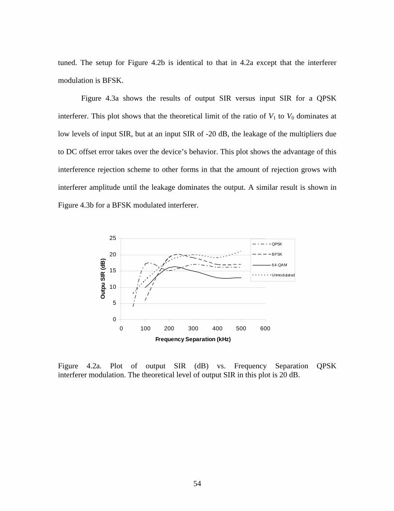
54
tuned. The setup for Figure 4.2b is identical to that in 4.2a except that the interferer
modulation is BFSK.
Figure 4.3a shows the results of output SIR versus input SIR for a QPSK
interferer. This plot shows that the theoretical limit of the ratio of V1 to V0 dominates at
low levels of input SIR, but at an input SIR of -20 dB, the leakage of the multipliers due
to DC offset error takes over the device’s behavior. This plot shows the advantage of this
interference rejection scheme to other forms in that the amount of rejection grows with
interferer amplitude until the leakage dominates the output. A similar result is shown in
Figure 4.3b for a BFSK modulated interferer.
0
5
10
15
20
25
0 100 200 300 400 500 600
Frequency Separation (kHz)
Out
pu S
IR (d
B)
QPSK
BFSK
64-QAM
Unmodulated
Figure 4.2a. Plot of output SIR (dB) vs. Frequency Separation QPSK interferer modulation. The theoretical level of output SIR in this plot is 20 dB.

55
0
5
10
15
20
25
0 100 200 300 400 500 600
Frequency Separation (kHz)
Out
pu S
IR (d
B)
QPSK
BFSK
64-QAM
Unmodulated
Figure 4.2b. Plot of output SIR (dB) vs. Frequency Separation, BFSK interferer modulation. The theoretical level of output SIR in this plot is 20 dB.
-10
-5
0
5
10
15
20
25
-50 -40 -30 -20 -10
Input SIR
Out
put S
IR
QPSKFSKQAMModeled
Figure 4.3a. Plot of output SIR vs. input SIR, QPSK modulated interferer. The modeled result assumes -45 dB of leakage in the multipliers. The frequency separation is 200 kHz. The QAM result for this case did not yield an appreciable output SIR except for 1 value of amplitude, and is therefore not shown.

56
-15
-10
-5
0
5
10
15
20
25
30
35
-50 -40 -30 -20 -10
Input SIR
Out
put S
IR
QPSKFSKQAMModeled
Figure 4.3b Plot of Output SIR vs. input SIR, BFSK modulated interferer. The modeled result assumes -45 dB of leakage in the multipliers. The frequency separation is 400 kHz and the modulation rate is 100 kHz.
It was found experimentally that as the modulation rate of the interferer
approaches and surpasses the frequency separation of the two signals, an intermodulation
product arises in the main signal. The intermodulation rejection is defined as the ratio of
side lobe power in the interfering input signal to the side lobe power in the desired output
signal. A plot of the level of intermodulation rejection versus the ratio of symbol rate to
frequency separation is given in Figure 4.4. This plot shows that the intermodulation
becomes significant as the ratio approaches and exceeds one. The desired signal is
unmodulated for this figure, and the modulation type for the interferer is varied. A
sample spectral plot for the reason that this residual modulation occurs is shown in Figure
4.5.

57
A significant observation stems from this plot. If we take the point at which the
modulation rate is half of the frequency separation and QPSK is employed, there is a side
lobe of the interfering signal that resides at the center frequency of the intended signal.
Figure 4.4 shows that the intended signal can still be recovered with an intermodulation
rejection of greater than 10 dB, even when the side lobe of the interferer is greater than
the main lobe of the intended signal at the intended signal’s center frequency.
0
5
10
15
20
25
30
35
0 0.5 1 1.5 2Ratio of Symbol Rate to Frequency Separation
Inte
rmod
ulat
ion
Rej
ectio
n (d
B) QPSK
FSKTheoretical
Figure 4.4 Plot of Intermodulation Rejection (dB) vs. Ratio of Symbol Rate to Frequency Separation.

58
-30
-20
-10
0
0 100 200 300 400
frequency (kHz)
Pow
er O
ut o
f Bra
nch
2 (d
Bm
)
Figure 4.5 Plot of Output Power in Branch 2 vs. frequency. The difference frequency for this plot is 150 kHz. The residual intermodulation is caused by the asymmetry about the difference frequency caused by the high pass filter in Branch 2.
V. Conclusions
The interference cancelling scheme shown in Figure 4.1 has been analyzed
analytically and experimentally. Experiments confirm its ability to reject a constant
amplitude, high-power, near-in-frequency interferer in a manner that is proportional to
the ratio of interferer to signal, as shown in Figure 4.2. Known limitations of this device
are the input leakage in the multiplier for very high interference levels (greater than 25
dB), and intermodulation on the primary signal when the modulation rate of the interferer
approaches the frequency separation between the two signals.
This work is expected to find application in dynamic frequency allocation. A
secondary user of the spectrum could communicate very close in frequency to a high-
powered primary user such as an FM transmitter while maintaining a high quality of

59
service and a low interference level for the FM band. Other applications include control
of an interfering signal that emerges at a frequency near an ongoing communication. The
strength of this system is that the amount of interference rejection grows with a decrease
in the input signal to interference ratio. It is therefore most suitable in cases where one
man-made interference source is the primary obstacle to signal detection or
communication in a narrow band of spectrum.
References
[4.1] J. Simoneau and L.W. Pearson, “Multitone Feedback through Demodulating Log Detector for Detection of Spurious Emissions in Software Radio.” Accepted, IEEE Trans. Circ. and Sys.
[4.2] D.K. Weaver, "A third method of generation and detection of singlesideband signals," Proc. IRE, vol. 44, Dec., 1956, pp. 1703-5.

60
CONCLUSIONS
Each paper presented in this dissertation represents an improvement to software
defined radio employing digital compensation for radio frequency impairments. In the
first paper, a means for real-time feedback of radio frequency (RF) properties of an RF
transmitter was derived. The demodulating log detector was found to have the useful
property of proportionality to the ratio of a high power signal to a lower-power signal at
the difference frequency between the two signals.
In the second paper, this property was employed to enhance the image rejection of
an IQ upconverter. Employing digital feedback through the log detector in a linear
feedback control loop, the image rejection of an IQ upconverter was improved from 35
dB without feedback to greater than 65 dB with the feedback employed. It was found that
the bandwidth of this scheme is limited only by the IQ mixer itself, not the feedback
network.
In the third paper, the bandwidth of an IQ mixer was enhanced employing a
baseband compensation scheme. Employing this compensation, the bandwidth of a
commercial off-the-shelf IQ mixer was extended from 8-12 GHz (40%) to .75-20 GHz
(186%), and the magnitude and phase mismatch was improved from + 1dB and +7
degrees to + 0.3dB and +1.8 degrees, respectively. Employing this scheme in concert
with the one provided in the second paper, it is possible to achieve a high level of image
rejection over a wide bandwidth beginning with an IQ mixer that is relatively narrow in
bandwidth and possesses only a moderate level of image rejection.

61
In the fourth paper, the log detector behavior that was derived in the first paper is
employed to reject a high-power, near-in-frequency interferer. Employing this scheme, an
output signal to interference ratio of greater than 10 dB is demonstrated for an input
signal to interference ratio of -10 to -35 dB and a frequency separation between signal
and interferer of only 2 kHz. If this result were employed in a frequency-agile radio, it is
possible that the channel-to-channel spacing could be greatly improved, leading to a
much more efficient utilization of the RF spectrum.

62
APPENDIX
Programmable Logic Implementation
Chapters two through four of this dissertation each involved some level of
programmable logic implementation. As has been described, this was performed
employing the Lyrtech SignalMaster platform which contains a Xilinx Virtex II field
programmable gate array (FPGA), and a Texas Instruments C67x digital signal processor
(DSP) chip. The method for programming these devices was to build block diagrams in
Matlab Simulink which were then compiled to the proper code for the selected processing
device. Xilinx System Generator was employed to perform the compilation to the Virtex
II FPGA, while the Lyrtech DSPlink compiled the block diagrams to C code for the
commands to be executed in the DSP. Programmable logic is broken down into three
sections: FPGA implementation for the results of Chapter Two, FPGA and DSP
implementation for Chapter Three, and FPGA implementation for Chapter Four.
FPGA Implementation for Chapter 2
The overview of FPGA implementation for this paper is shown in Figure A.1.
This figure shows the feedback being fed through an analog to digital converter (A/D),
the Discrete Fourier Transform being taken (as shown in Figure A.2), followed by the
magnitude and phase correction (as shown in Figure A.3), followed by integration and
waiting for correction (as shown in Figure A.4), followed by IF upconversion of the
correction (as shown in Figure A.5), and finally summing the corrected and initial signals
(as shown in Figure A.6).

63
Figure A.1. Overview of FPGA Implementation for Chapter Two.
Figure A.2. Discrete Fourier Transform Implementation. Inputs are the feedback signal and IF frequency. The IF frequency is doubled in order to implement the DFT at twice the IF. The sine and cosine at this frequency are then correlated with the input and accumulated to yield the real and imaginary value of the DFT at twice the IF.

64
Figure A.3. Magnitude and Phase Correction. The constant multiplication is performed on the real imaginary parts of the DFT, while the value of phase shift is drawn from a control register, and the phase shift is applied by a complex multiplication, followed by summing to form the new real and imaginary parts of the phase-shifted DFT.
Figure A.4. Wait for Correction and Integration. The wait for correction is applied by a multiplexer that alternated feeding a zero and the DFT result into integrators for the real and imaginary parts of the signals.
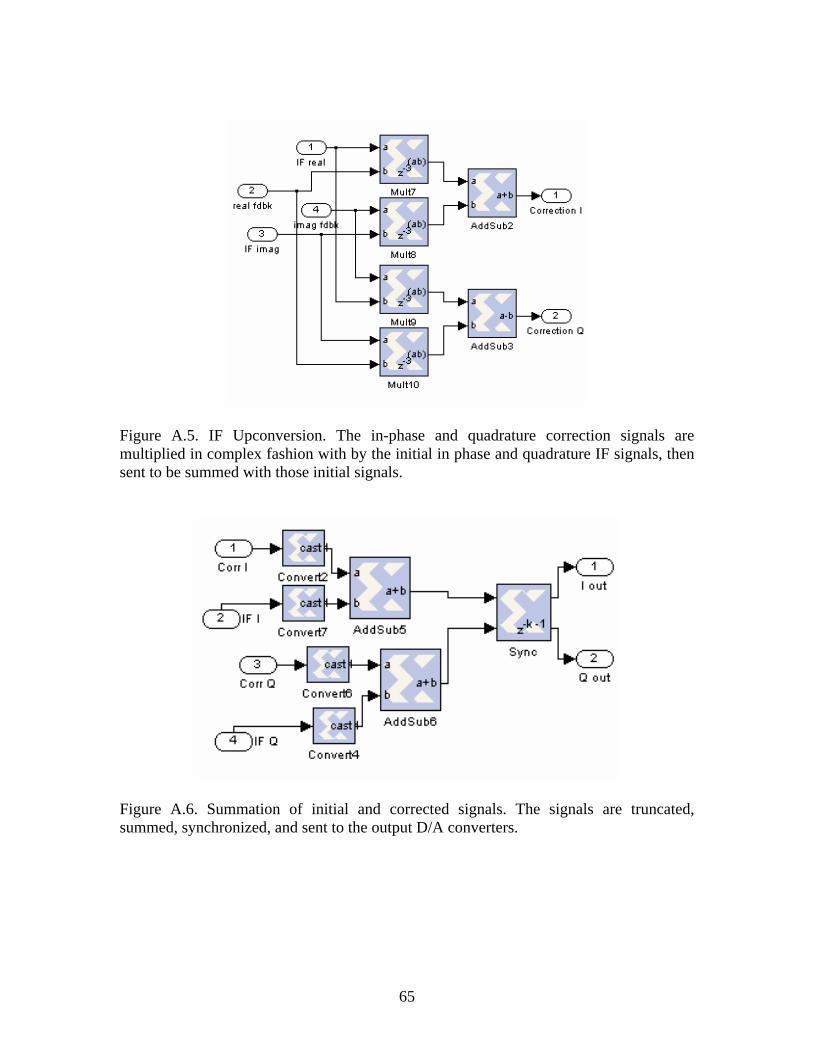
65
Figure A.5. IF Upconversion. The in-phase and quadrature correction signals are multiplied in complex fashion with by the initial in phase and quadrature IF signals, then sent to be summed with those initial signals.
Figure A.6. Summation of initial and corrected signals. The signals are truncated, summed, synchronized, and sent to the output D/A converters.

66
FPGA and DSP implementation for Chapter Three
Figure A.7 shows the FPGA implementation for Chapter Three, which is simply
the four multipliers fed by the DSP calculation based on magnitude and phase mismatch,
which is shown in Figure A.8.
Figure A.7. FPGA Implementation for Chapter Three. Four multipliers are fed by the DSP registers and an IF signal. These are then summed and sent to the D/A output for the in-phase and quadrature branches of the upconverter.

67
Figure A.8. DSP Implementation for Chapter Three. The four compensation constants are those derived in Chapter 3, based on the parameters A and φ.
FPGA Implementation for Chapter Four
Figure A.9 is an overview of the FPGA implementation for Chapter Four. This
implementation implements four different modulation schemes on a desired signal. Not
pictured in this figure is the implementation for the interferer, which is identical in
implementation to the desired signal. The four different types of modulation are
quadrature phase shift keying (QPSK), as shown in Figure A.10, 64-ary quadrature
amplitude modulation (64-QAM), shown in Figure A.11, Binary Phase Shift Keying
(BPSK), shown in Figure A.12, and Binary Frequency shift keying (BFSK), shown in
Figure A.13. The modulation type is selected by a register input, and the signal is then
unconverted to an IF and conditioned for single sideband output as shown in Figure A.14.

68
Figure A.15 shows the setting of the relative amplitude, and then the desired signal is
summed with the interferer and put on the D/A for upconversion.
Figure A.9. FPGA Implementation for Chapter Four. The input register selects the type of modulation. In phase and quadrature signals are generated, upconverted to the proper IF, the relative amplitude of the desired signal is set, and then summed with the interferer for upconversion.
Figure A.10. QPSK Modulation. The random input bit stream is generated by a linear feedback shift register, and upsampled to give the proper bit rate to feed the Mux and select between positive or negative input. An identical circuit is employed for the quadrature modulation with the LFSR seed varied.

69
Figure A.11. 64-QAM Modulation. The LFSR generates a random bit stream which is fed to the Mux to select between eight possible amplitudes. An identical circuit feeds the quadrature output, with the seed of the LFSR varied to give an independent bit stream.
Figure A.12. BPSK Modulation. Implementation is identical to QPSK, except that the output here is fed to both in-phase and quadrature outputs.

70
Figure A.13. BFSK Modulation. The LFSR is identical to those previously mentioned. This bit stream selects between the two frequencies, which are fed to the intermediate frequency synthesizer if FSK is selected.
Figure A.14. IF Upconversion. The IF frequency is set to 1 MHz and the frequency is shifted if FSK is selected, then multiplied by the in-phase and quadrature inputs. The sum and difference are taken on the signals to generate 90 degrees of phase shift, thereby conditioning the signal for single-sideband output.

71
Figure A.15. Amplitude Set. The relative amplitude of the desired and interfering is set by a register input and multipliers, and the output is then summed with the interferer and sent to the IQ upconverter.


