
Full Paper
In Situ Doped Polyaniline Nanotubes forApplications in Flexible Conductive Coatings
Sarang P. Gumfekar, Wenjie Wang, Boxin Zhao*
In-situ doped polyaniline nanotubes were fabricated and investigated in term of theirmorphological, thermal and electrical properties at varied doping levels. Different from thecommon post-doping of polyaniline base to form its emeraldine salt, the aniline monomers weredirectly converted into conductive emeraldine salt during synthesis by dropwise addition of
the dopant and oxidants. This process resulted in auniform and stable protonation of the polyanilinewith good electrical conductivity. Furthermore, itwas found that the crystalline conductive polyani-line nanotubes have a good flexibility whenamalgamatedwith polyvinyl alcohol, showing theirpotential as flexible conductive coating materials.S. P. Gumfekar, W. Wang, B. ZhaoDepartment of Chemical Engineering, Waterloo Institute forNanotechnology, University of Waterloo, 200 University AvenueWest, Waterloo, ON, Canada N2L3G1E-mail: [email protected]. WangState Key Laboratory of Explosive Science and Technology, Schoolof Mechatronical Engineering, Beijing Institute of Technology,Beijing 100081, P. R. China
� 2014 WILEY-VCH Verlag GmbH & Co. KGaA, Weinheim wileyonlinelibrary.c
Early View Publication; these are NOT th
facial polymerization,[14] electrochemical polymeriza-[15] [4,16]
1. Introduction
Polyaniline (PANI) is one of themost promising electrically
conductive polymers in various fields of electronics, such as
sensors,[1,2] electromagnetic interference shielding,[3,4]
super-capacitors,[5–7] diodes,[8] and transducers.[9] This
polymer exhibits metallic behavior in terms of electrical,
magnetic, and optical properties and retains the properties
of conventional polymers such as flexibility and tempera-
ture-dependent viscosity. Nanostructured PANI has
attracted a great deal of interest because of its tunable
conductivity switching between insulator and conductor,
nontoxic properties, and good environmental and chemical
stability.[6,10–12] Different forms of PANI, such as nano-
particles, nanotubes, and nanowires, have been prepared
by various physical and chemical synthesis methods.
Physical methods include electro-spinning[13] and various
deposition techniques, while chemical routes include
inter
tion, and emulsion polymerization.
The electrical conductivity of PANI is obtained typically
by doping the PANI emeraldine base,[17,18] whose backbone
structure is illustrated inFigure1a.Thedegreeofdopingcan
be controlledbyaciddopingorbasededoping.Hydrochloric
acid is widely used as a dopant for PANI because of its
availability and simple reaction chemistry. Doping in PANI
has a significant impact on its potential applications in
nano-electronics and nano-devices. Morales et al. showed
that the increase in substitution on PANI backbone
decreased the electronic conjugation, which resulted in
thedecrease of conductivity.[19] Thus, dopingneedsbedone
without affecting the backbone structure of PANI. It has
also been shown that un-doped PANI forms aggregates due
to such inter-chain interactions as the hydrogen bonding
betweenthe imineandaminenitrogensitesontheadjacent
PANI molecules.[20] However, the effects of the degree of
doping on the electrical conductivity particularly in the
conductive regime are much less investigated, and the
bonding nature of chloride ions with PANI backbone chain
is still unclear. Better understanding of these effects is
important for the potential applications of PANI as, for
example, conductive fillers in the development of electrical
conductive adhesive and coatings.
In recentyears, therehavebeenincreasinglydemandsfor
the development of PANI-filled conductive adhesive films
and coatings to partially replace the conventional metallic
Macromol. Mater. Eng. 2014, DOI: 10.1002/mame.201300354 1om
e final page numbers, use DOI for citation !! R

Figure 1. a) Backbone structure of polyaniline emeraldine base indicating reduced and oxidized form and b) The scheme of formingpolyaniline emeraldine salt from aniline monomer with ‘‘in situ’’ doping of HCl in presence of ammonium persulfate. Chloride ions areattached to imine nitrogen of polyaniline backbone.
www.mme-journal.de
S. P. Gumfekar, W. Wang, B. Zhao
2
REa
fillers so as to make the process more environmental
friendly and enhance flexibility of the films for the varied
applications in LCD, flexible display, and diodes. However,
PANIhas limited solubility inorganic solvents and inwater.
It has been shown that PANI can be made water soluble
using bi-functional water soluble dopants.[21,22] But the
electrical performance of common thin film and sensor
applicationsofwater solublePANIwasrelativelypoor.[23,24]
Solubility of PANI in organic solvents has also been
studied.[25–27] The PANI in base form can be made soluble
in organic solvents such as NMP, DMSO, and DMF. Widely
studied dopant DBSA could result in only 8% solubility of
PANI.[27] In general, PANIhas apoorprocessability,which is
amajor barrier in the fabrication of PANI films. In addition,
amorphous PANI has a relatively lower conductivity
than the metallic fillers; this low conductivity limits its
application. Because of these limitations, there has been a
continuous interest in the synthesis and applications of
crystalline PANI nanotubes. Crystalline PANI has a much
better conductivity than the amorphous one and has the
potential to replace metallic fillers in more applications.
One-dimensional PANI nanotubes allow an efficient
transport of electrical carriers throughout the conductive
network, which is highly desired when integrated nano-
scale devices involve the moving charges.[28]
In this study,wereport the fabricationof crystallinePANI
nanotubes with varied doping levels. In contrast to the
common post-doping of PANI base to form its emeraldine
salt, the PANI nanotubes were in situ doped by HCl during
the polymerization at varied dopant to monomer (D/M)
Macromol. Mater. Eng. 2014, DOI
� 2014 WILEY-VCH Verlag Gmb
rly View Publication; these are NOT the final pag
ratios. This process resulted in a uniform and stable
protonation of the PANI with good electrical conductivity.
The relations between the D/M ratios and PANI spectro-
scopic and structural features, crystallinity, and electrical
conductivity were systematically investigated to provide
fundamental insights to the roles of the dopant in the
structure and properties of the PANI nanostructures. We
also demonstrated the good dispersion ability of in situ
doped PANI nanotubes in polyvinyl alcohol (PVA) solutions
and the potential applications by coating them onto a
polyethylene terephthalate (PET) substrate to form a
flexible electrically conductive film.
2. Materials and Experiments
2.1. Materials
Aniline (99.9%, corrected for water content) was purchased
from J.T. Baker, USA, and stored in a dark place to avoid
photo-polymerization. Ammonium persulfate (98%) was
procured from EMD Chemicals, which contained an
insoluble matter less than 0.005%. Polyoxyethylene sorbi-
tan monooleate and PVA (99þ% hydrolyzed) of molecular
weight 146 000–186 000 Da was purchased from Sigma
(USA). Hydrochloric acid (37%) was used as a doping agent
and was purchased from Thermo Fisher Scientific. All the
glassware were cleaned prior to use; they were soaked in a
1M solution of sodium hydroxide for 24h, neutralized with
acetic acid, and then rinsed with DI water. The DI water
(resistivity> 10 MV cm at 25 8C; total organic carbon <20
: 10.1002/mame.201300354
H & Co. KGaA, Weinheim www.MaterialsViews.com
e numbers, use DOI for citation !!

In Situ Doped Polyaniline Nanotubes for Coating Applications
www.mme-journal.de
ppb) was obtained using the RiOs-DI Clinical system (Milli-
Pore Corporation).
2.2. Fabrication of Polyaniline Nanostructures
Amonomer solution, 0.1M aniline was prepared in 1M HCl,
wherein the 1M HCl was prepared in de-ionized water. A
surfactant solution of polyoxyethylene sorbitan mono-
oleate (0.08M) was prepared in ethanol; it has a faint hazy
yellow color. The monomer and surfactant solutions were
sonicated separately and then were mixed together and
poured into a 1 L reactor, equipped with a temperature-
controlled jacket. As-prepared mixture was brought to 4 8Cand stirred vigorously with a magnetic needle to form an
emulsion mixture. To start the reaction, 0.05M solution of
ammonium persulfate in 1M HCl was continuously added
for a half hour to the emulsified mixture of aniline.
Polymerization of aniline is a type of chemical oxidative
polymerization of aniline; it is exothermic. We carried out
the reactionat4 8Cbycirculatingcoolantaroundthereactorandprecisely controlling the rateofadditionofAPSsolution
to the aniline solution under vigorous stirring. Polymeriza-
tion of aniline continued for 2h according to the scheme
depicted in Figure 1b. Reactionwas carried outwith dopant
tomonomer (D/M) ratios of 8, 16, and 50 for the studyof the
effect of dopant. The PANI was purified by the centrifuga-
tion of the reactionmixture followed bywashing profusely
with deionized water and acetone for at least four times to
remove the traces of surfactant, unreacted aniline, and
unreacted HCl. Purified PANI was dried under dynamic
vacuum for 24h to remove the washing solutions.
2.3. Chemical, Structural, Thermal, and Electrical
Characterizations
Polyaniline samples were characterized in terms of their
chemical, structural, morphological, optical, and thermal
properties. Fourier-transform infrared spectra (FTIR) of the
PANI samples (three repeats) were recorded using a Varian
640-IR with 100 scans per spectrum at 2 cm�1 resolution
between the wavenumbers 400–2 000 cm�1. The spectra
were corrected for the presence of moisture and CO2 in the
optical path. Morphological characteristics of PANI nano-
tubeswere examinedat various locations of the samples by
field emission scanning electron microscope (SEM) using
LEO FE-SEM 1530 (Carl Zeiss NTS), operated at 10 kV. The
samples were prepared by depositing one drop of the
sonicated PANI containing solution on the conductive
carbon tape and dried in air for 24h, followed by gold
sputtering for 120 s.
High-angle annular dark-field (HAADF) transmission
electron microscopy images combined with energy disper-
sive X-ray spectroscopy (Oxford EDX detector) data were
acquired on a FEI Titan 80–300 TEM (FEI company,
Macromol. Mater. Eng. 2014, DO
� 2014 WILEY-VCH Verlag Gmwww.MaterialsViews.com
Early View Publication; these are NO
Eindhoven, The Netherlands), equippedwith a CEOS image
corrector and operated at 80 kV. To prepare TEM samples,
one droplet of dilute dispersion of PANI nanotubes in
methanol (1mgmL�1) was dropped on a lacey/holey
carbon copper grid and dried for 1/2 h in air. Ultraviolet–
visible spectroscopy of the PANI samples was performed
(three repeats) using aUV–Vis spectrophotometer (UV–Vis)
(UV-2501 pc, Shimadzu). For this, PANI was dissolved in
DMF; the solutionwas placed in a quartz cuvette of 1.00 cm
path length. Weight loss and subsequent degradation
mechanism of doped PANI in powder form was studied
using thermo-gravimetric analysis (TGA) (TA instrument,
Q500-1254). Samples of about 4mg were placed in a
TGA sample pan. Dynamic scan was performed from 25 to
800 8C with a heating rate of 10 8Cmin�1 under nitrogen
atmosphere.
To measure the bulk electrical contact resistivity of the
synthesized PANI nanotubes, they were uniformly spread
onto a piece of non-conductive Scotch tape under a slight
finger pressure to form a compact film of 300mm thick.
Thefilmdimensionswere 1 cm� 3 cm. Eight to ten samples
were characterized at different locations on the film.
The resistivity was measured by a four-point probe setup
consisting of a probe fixture (CascadeMicrotech, Inc.) and a
source meter (Keithley 2440 5A Source Meter, Keithley
Instruments, Inc.). The sheet resistance of the PANI nano-
tubes film (Rs) was estimated by measuring the drop in
voltage when a constant current of 100mA was applied.
The electrical resistivity (r) of the film of PANI nanotubes
was calculated using the following equation:
I: 10.10
bH & C
T the
r ¼ Rst ¼ ptln 2
� �VI V cm ð1Þ
where t is the thickness of samples, and I and V are the
applied current and the measured voltage, respectively.
2.4. Fabrication and Characterization of Flexible
Electrically Conductive Films
Tomake PANI coating on a flexible surface, a pre-measured
quantity of PANI nanotubes was uniformly dispersed in a
PVA aqueous solution (10wt%) under intense sonication.
The PVA solution was prepared by dissolving PVA in de-
ionized water at 80 8C in vigorously stirred environment.
Note that the optical transparency of PVA can be affected
due to the overheating,whichwas avoided in ourwork. The
overheating might degrade the polymeric chains resulting
in yellowish hazy color. PET overhead transparency (Xerox
Corporation, NY, USA)was chosen as a substrate for casting
the film of PVA–PANI solution; the casting of 1 g mixture
was performed using a spin-coater at 500 RPM. The
thickness of the film coated onto PET substrate was
measured by a Vernier caliper to be 300� 15mm. As-casted
02/mame.201300354
o. KGaA, Weinheim 3
final page numbers, use DOI for citation !! R

www.mme-journal.de
S. P. Gumfekar, W. Wang, B. Zhao
4
REa
conductive films were dried in air at room temperature for
12h to allow the firm bonding of PANI nanotubes onto the
substrate. The PANI-coatedfilmwasvisually examinedand
physically bent and scratched to check its quality and
durability. The bulk resistivity of PANI-coated PET film
was measured using the same four-point probe setup as
described before.
3. Results and Discussion
3.1. Fabrication of Polyaniline Nanotubes
Polyaniline nanotubes were fabricated using the mini-
emulsion polymerization method with polyoxyethylene
sorbitanmonooleate (Tween 80) as the surfactant. Figure 2
illustrates the experimental setup inwhich the oxidantAPS
and dopant HCl were added dropwise into the monomer
aniline solution. Although the mechanism is not fully
understood, it has been shown that the surfactant
molecules form nano-sized micelles in the solutions,
containing the aniline monomers; the polymerization of
aniline occurred in the confined spaces of the micelles
as initially reported by Wan.[29,30] During the reaction, a
transition of color from blue to green was observed,
suggesting the formation of emeraldine salt of PANI. We
observed that an increase in dopant to monomer (D/M)
ratio caused the green color to become darker, suggesting
that the dopant HCl might increase the rate of polymeriza-
Figure 2. Schematic set-up of the polymerization of anilines: a) dropwHCl, b) temperature controlled jacketed reactor, c) as-synthesized puof polyaniline nanotubes in DMF at different dopant to monomeremeraldine salt of polyaniline.
Macromol. Mater. Eng. 2014, DOI
� 2014 WILEY-VCH Verlag Gmb
rly View Publication; these are NOT the final pag
tion of aniline. Figure 2d shows typical images of stable
dispersion of PANI at different D/M ratios. It can be
seen that the increase in the D/M ratio caused a color
transformation from bluish green to dark green. A bluish
green color in the sample with D/M¼ 8 implied the
presence of emeraldine base along with emeraldine salt
while its disappearance in the later two images signified
the complete transformation into emeraldine salt. Thus,
the increase in dopant caused increased formation of
emeraldine salt of PANI.
Thereare twokey features in the fabrication. Thefirstone
is the ‘‘in situ’’ HCl doping. In contrast to the post-doping of
PANI base to form its emeraldine salt, the ‘‘in situ’’ doping
process directly converted aniline monomers into the
emeraldine salt during the polymerization to obtain
homogeneous doping. This process allows the dopant
molecules and PANI backbone to bond firmly due to
electrostatic forces between them.[31–33] This acidic condi-
tion also helped to stabilize the surfactant micelles. The
second feature involved the suppression of secondary
nucleation of PANI on the already formed nanotubes of
PANI by the dropwise addition of APS with vigorous
stirring. Our preliminary experiments where all APS was
added to aniline at once (without stirring) showed a rapid
sedimentation of aggregated PANI particles from solution
because secondary nucleation took place on the surface of
newly formed PANI and resulted in the formation of strong
aggregates.[34] Li and Kaner[35] have shown that homoge-
neous nucleation of PANI results in formation of nanotubes
ise addition of an aqueous solution of the oxidant APS and dopantrified polyaniline nanotubes, and d) images of the stable dispersion(D/M) ratios; the increasing dark color signifies the formation of
: 10.1002/mame.201300354
H & Co. KGaA, Weinheim www.MaterialsViews.com
e numbers, use DOI for citation !!

In Situ Doped Polyaniline Nanotubes for Coating Applications
www.mme-journal.de
while heterogeneous nucleation causes formation of
granular particles.
The resultant PANI nanotubes were analyzed using SEM
at variedmagnifications as shown in Figure 3a–c. Although
the SEM images at the lowmagnification (Figure 3a) appear
to have some particulate materials, the higher magnifica-
tion SEM images (Figure 3b,c) do not show any particles. It
can be seen that PANI nanotubes form entangled network
in bulk state because of interchain and/or intrachain
interactions. This type of interconnecting network is
desired to obtain uniform electrical conductivity and
flexibility. Figure 4a,c,e are typical TEM images of the PANI
nanotubes formed at various dopant to monomer (D/M)
ratios, where a single PANI nanotubes at highermagnifica-
tion is shown in the inset. It can be seen that the PANI
nanotubes are hollow from inside and exhibit distinct
crystalline boundary as shown in the inset nanotubes.
Individual nanotubes were joined together into larger
secondary structures (mainlyone-dimensional) on theends
and surface of the primarily grown PANI nanotubes. Thus,
in the interconnecting network observed SEM image of
Figure 3, the nanotubes are physically entangledwith each
other. The length and diameter of the PANI nanotubeswere
estimated from these TEM images, and found to be
215� 19nm and 40� 12nm, respectively for both samples
withD/M¼ 8andD/M¼ 16. The length anddiameter of the
PANI nanotubes were found to be 134� 15nm and
31� 6nm, respectively for samples of D/M¼ 50.
Figure 4b,d,f show the corresponding selected area
electron diffraction (SAED) patterns. They show the
alternate dark and bright fringes, which can be attributed
to the crystallinity of the nanotubes. Grain boundaries
along the different crystalline planes can also be seen from
the HRTEM images of PANI confirming the polycrystalline
nature of the nanotubes. Furthermore, a detailed examina-
tion of the TEM images revealed some secondary growth of
PANI as indicated by the arrows in Figure 4c,e. Excessive
growth of secondary structures could result in branching
of nanotubes, which has been successfully inhibited by
the controlled addition of oxidant APS.
Figure 3. SEM images of bulk, powdered polyaniline synthesized withviews of entangled polyaniline nanotubes.
Macromol. Mater. Eng. 2014, DO
� 2014 WILEY-VCH Verlag Gmwww.MaterialsViews.com
Early View Publication; these are NO
3.2. Spectroscopic Analysis of Polyaniline
Nanostructures
Chemical characteristics of PANI nanostructures and the
effect of dopingwere examinedbyFT-IR. Figure 5 shows the
FT-IR spectra of PANI for dopant tomonomer (D/M) ratio of
8, 16, and 50. Distinct characteristics of doped samples are
associated with emeraldine salt of PANI. The peak at
621 cm�1 is associated with S—C vibrations,[36–38] where
theAPS is consideredas theexpected sourceof sulfuratoms.
The peak at 849 cm�1 is related to the out-of-plane
stretching vibration of 1,4-disubstituted benzenoid ring,
which is a para-coupling structure.[32] The minor peak at
1 059 cm�1 is associated with the sulfate ion stretching
vibrations,[29,33] while the peak at 1 024 cm�1 is ascribed to
S55Ovibrations.[34] Appearance and subsequent increase in
the absorption peak at 1 194 cm�1 is associated with the
vibration modes of N55Q55N. The increased absorption is
ascribed to the increase in PANI content with enhanced
doping.[4] The peak at 1 276 cm�1 is attributed to C—H in-
planebendingmode. Thepeakat 1367 cm�1 is attributed to
C—Nþ* stretching vibration in a polaron structure;[4] this
absorption band is correlated to p-electron delocalization
induced in the PANI bydopingprocess. Itwas observed that
delocalization of p-electrons (1 367 cm�1) increased with
increase in dopant to monomer ratio, suggesting the
conjugation and subsequent increase in interconnecting
network of PANI, which caused stronger delocalization of
p-electrons. Additionally, there are two peaks at 1 535 and
1520 cm�1,which are attributed to the stretching vibration
of quinoid and benzenoid ring, respectively.[39,40] The peak
at 1 520 cm�1 undergoes a minor red shift with increased
doping levelsbut thepeakat1535 cm�1 is fixedbecause the
quinoid rings are widely separated – see Figure 1a. There is
another characteristic peak at 1 640 cm�1 due to stretching
vibrations of C55C; this peak shifted to higher wave-
numbers (or lower wavelengths) with the increase in
dopant concentration. This shift and increased absorption
were attributed to increased protonation in PANI due to the
dopant molecules.[41]
D/M¼ 50 with increasingmagnification (a! c), showing the close-in
I: 10.1002/mame.201300354
bH & Co. KGaA, Weinheim 5
T the final page numbers, use DOI for citation !! R

Figure 4. HRTEM images and corresponding selected area diffraction pattern (SAED) of polyaniline nanotubes with (a, b) D/M¼8, (c, d)D/M¼ 16, (e, f) D/M¼ 50. Arrows in (c) and (e) show the probable sites of secondary nucleation.
www.mme-journal.de
S. P. Gumfekar, W. Wang, B. Zhao
6
REa
We noticed that there is a peak at about 1 600 cm�1 for
D/M¼ 50butnot forD/M¼ 16. It canpossibly be attributed
to non-symmetric stretching of benzene ring, which can
be observed in the presence of adsorbed H2O on PANI
backbone. Thus, we suspect that some water molecules
Macromol. Mater. Eng. 2014, DOI
� 2014 WILEY-VCH Verlag Gmb
rly View Publication; these are NOT the final pag
mayhave been adsorbed to the highly doped PANI. Overall,
the observed FTIR features for D/M¼ 8 areweaker than the
other two because its polymerization is not completely
triggered whereas para-coupling (849 cm�1) and polaron
structure (1 276 cm�1) peaks appear with increased D/M
: 10.1002/mame.201300354
H & Co. KGaA, Weinheim www.MaterialsViews.com
e numbers, use DOI for citation !!

Figure 5. FT-IR spectra of polyaniline nanotubes with different dopant to monomer (D/M) ratios.
In Situ Doped Polyaniline Nanotubes for Coating Applications
www.mme-journal.de
ratio because of aniline polymerization toward emeraldine
salt.[38] The FTIR results suggest that the dopant to
monomer ratio has an important role in the polymerization
of aniline. Later, we will discuss the effect of this ratio on
optical and electrical properties of the PANI.
Figure 6. UV–visible spectra of polyaniline nanotubes showingdistinct peaks at �330 and �450nm with varied dopant tomonomer ratios (D/M).
3.3. Optical Characteristics of Polyaniline
Nanostructures
UV–Vis absorption spectrum for each dopant to monomer
ratio is shown in Figure 6, displaying three distinct peaks
at low wavelengths and one ‘‘free-carrier’’ tail at high
wavelengths. The absorption peaks and tail are typical
features of PANI at its emeraldine oxidation state. The first
characteristic peak is at �330nm, which can be assigned
to p� p� transition of benzenoid rings and to the charge-
transfer-exciton transition formed in benzenoid and
adjacent quinoid ring. The other peak is at �450nm,
signifying the existence of polaron–p� transition.[10,17,40]
The third absorption peak at higher wavelengths is the
signature of p-polaron transition.[6,17] The relative posi-
tions of these absorption peaks indicated the different
electron transitions of the PANI backbone and provided
insights to the protonation of the PANI backbone and its
electrically conductive state.
Addition of protons to the PANI chain results in
subsequent formation of polarons, which increases its
electrical conductivity. A comparison of the spectra of PANI
of varied dopant to monomer ratios (and subsequent
increase in protonation) revealed a redshift of the lower
wavelength absorption peak from 332 nm-to-326 nm-to-
Macromol. Mater. Eng. 2014, DO
� 2014 WILEY-VCH Verlag Gmwww.MaterialsViews.com
Early View Publication; these are NO
319nm. The similar trend of redshift was observed for
the second peak from 449 nm-to-438 nm-to-431nm. We
attributed this redshift to the possible increase in the
molecularweight of PANIwith the increase in protonation.
The spectra also allowed us to obtain some indirect
information about the conformation of PANI nanotubes.
PANI nanotubes can exhibit two conformations, i.e.,
‘‘compact coil’’ and ‘‘extended coil’’ conformations; the
compact coil has a significantly broad (long tail) polaron
absorption peak at �650nm while extended coil exhibits
intense absorption in near-infrared region.[42,43] UV–Vis
spectra suggested that as-synthesized PANI nanotubes
I: 10.1002/mame.201300354
bH & Co. KGaA, Weinheim 7
T the final page numbers, use DOI for citation !! R
www.mme-journal.de
S. P. Gumfekar, W. Wang, B. Zhao
8
REa
were in ‘‘compact coil’’ conformation; the increase in
dopant to monomer ratio decreased the character of
‘‘compact coil’’ conformation.[33,42,44]
3.4. Thermal Properties of Polyaniline Nanotubes
Distinct thermal features were observed in TGA of PANI as
shown in Figure 7. The temperature corresponding to
weight losswas calculated from the derivative data of TGA.
There are three major transitions or three types of weight
losses for all three curves. First, the PANI lost a certain
amount of weight below 125 8C. This weight loss was
attributed to the expulsion of unbound water, volatile
impurities, and gaseous HCl which could be physically
sorbed inpolymermatrix.[45–47] The secondweight losswas
observed between 200 and 300 8C. Thisweight loss has two
possible reasons: one is the removal of ‘‘linked’’water to the
PANI backbone that also acts as a secondary dopant; the
other reason could be the removal of small fragments of
PANI, which can decompose at lower temperature than the
main PANI chains. There might be possible cross-linking of
the polymeric chains during heating between 100 and
300 8C.[48] Thefinalweight losswas observed at the onset of
525 8C; and the slope of the thermo-gravimetric curve
between500and600 8Cwasfoundtobesteeper thanthatof
between 200 and 300 8C, indicating the structural changes
of PANI. We attributed this weight loss to the thermal
decomposition of main molecular chains of PANI. In
nitrogen atmosphere, these extended aromatic structures
decomposed and formed the coke. The residues at 800 8Caccounted for highly carbonized materials and thermally
stable species. It is worthwhile to note that the thermal
curves shifted to the upper right direction as the D/M
increased from 8 to 50, suggesting increased thermal
stabilization of PANI nanostructures at higher D/M ratios.
Figure 7. Thermo-gravimetric analysis of polyaniline withdifferent dopant to monomer ratios.
Macromol. Mater. Eng. 2014, DOI
� 2014 WILEY-VCH Verlag Gmb
rly View Publication; these are NOT the final pag
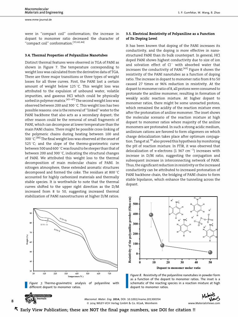
3.5. Electrical Resistivity of Polyaniline as a Function
of Its Doping Level
It has been known that doping of the PANI increases its
conductivity, and the doping is more effective in nano-
structured PANI than its bulk counterpart. In general, HCl
doped PANI shows highest conductivity due to size of ion
and solvation effect of Cl� with absorbed water that
increases the conductivity of PANI.[43] Figure 8 shows the
resistivity of the PANI nanotubes as a function of doping
ratio. The increase in dopant tomonomer ratio from 8 to 50
caused 27 times or 96% reduction in resistivity. At the
dopant tomonomer ratioof 8, all protonswere consumed to
protonate the aniline monomer, resulting in formation of
weakly acidic reaction mixture. At higher dopant to
monomer ratios, there might be some unreacted protons,
which remained the acidity of the reaction mixture even
after the protonation of aniline monomer. The inset shows
the molecular scenario of the reaction mixture at high
dopant to monomer ratios where majority of the aniline
monomers are protonated. In such a strong acidicmedium,
anilinium cations are favored to form oligomers on which
charge delocalization takes place after optimum conjuga-
tion. Tanget al.38 alsoproved thishypothesis bymonitoring
the pH of reaction mixture. In FTIR, it was observed that
delocalization of p-electrons (1 367 cm�1) increases with
increase in D/M ratio, suggesting the conjugation and
subsequent increase in interconnecting network of PANI.
Thus, the significant reduction inresistivityor the increased
conductivity can be attributed to increased protonation of
PANI backbone chain, the bridging of PANI chains to form
stable bipolaron, which enhance the tunneling across the
dopant.
Figure 8. Resistivity of the polyaniline nanotubes in powder formas a function of the dopant to monomer ratios. The inset is aschematic of the reacting species in a reaction mixture at highdopant to monomer ratios.
: 10.1002/mame.201300354
H & Co. KGaA, Weinheim www.MaterialsViews.com
e numbers, use DOI for citation !!

In Situ Doped Polyaniline Nanotubes for Coating Applications
www.mme-journal.de
3.6. Performance of Flexible Electrically Conducting
Coating
Thepotential applicationof the crystalline conductivePANI
nanotubes for the conductive flexible coatings was
investigated by examining the morphologies, mechanical
integrity, and electrical resistivity of PANI (dispersed in
PVA) coatings on PET films. Although there might be some
effects of film thickness on electrical properties of the
coating,[49] 300mmthick PANI films,which is typical for the
conductive coating applications, were employed in this
work to study the effect of morphology and doping levels.
The composite contained 50wt% as-synthesized PANI
nanotubes. Generally, non-uniform dispersion of filler in
polymer matrix results in poor electrical performance and
formation of distinct conductive domains[50,51] because of
the weak compatibility of fillers with polymer matrix and
undesired strong interactions between the filler particles.
To address this concern, we tested the dispersion of PANI
nanotubes in the PVA, a typical polymer binder and
antioxidant for PANI.[52] It was found that the PANI
nanotubes could be readily dispersed into the PVA aqueous
solution; and, a layer of the uniformdispersion can be spin-
coated on the surface of the PET substrate to form a PANI
coating of 300� 15mmthick. Recently, it was reported that
the entangled PANI structure has enhanced processability
inpolymer suspensions.[53] Thus, the crystalline conductive
PANI has a good film forming properties when used with
PVA. Perhaps, the HCl dopant present on the backbone
chain of PANI induced positive charges on the backbone
chains, resulting in electrostatic repulsion among the PANI
nanotubes in colloidal dispersion. Li and Kaner[28] obtained
the similar colloidal dispersion and attributed it to the
sufficiently acidic pHof the solution,which in turn signifies
the electrostatic stabilization.
Figure 9a shows an image of the as-fabricated PANI/PVA
coating, exhibiting a visually smooth and uniform surface.
The coated film was bent in 908 as shown in Figure 9b. No
wrinkles, cracks, and delamination were spotted on the
coatings, suggesting its mechanical robustness under
Figure 9. a) An image of as-fabricated conducting film, b) an image shthe flexible electrically conducting film showing the uniform dispers
Macromol. Mater. Eng. 2014, DO
� 2014 WILEY-VCH Verlag Gmwww.MaterialsViews.com
Early View Publication; these are NO
mechanical strains. The detailed surface morphologies
were examined using SEM; Figure 9c is one typical SEM
image showing the uniform dispersion and the entangled
network of PANI nanotubes, which is a desired property for
various uses in flexible electronics.
The electrical resistivity was characterized by the four-
point probe setup. The Figure 10 shows the resistivity as a
function of the dopant to monomer ratio for the PANI
(dispersed in PVA) coating on the PET substrate. As
expected, the electrical resistivity decreased as the D/M
ratio increased, showing a similar trend to that of the pure
PANI (see Figure 8). It is informative to notice the difference
in the reduction of electrical resistivity between PANI and
PANI/PVA. First, the resistivity of PANI/PVA conducting
coatingswasmuchhigher thanthatofonlyPANIbecauseof
the insulating nature of the PVA. Second, the increase in
D/M ratio from 8 to 50 caused 27 times reduction in
resistivity of PANI powder whereas 13 times reduction in
case of PANI/PVA. The observed resistivity of the film at
D/M¼ 50 is 1.72E6. This differencemaybe explained by the
insulating effect of the PVAmatrix.Note that the PANI/PVA
films are uncured in this study, and their properties may
change when exposed to different environmental con-
ditions. Future studies may need to use crosslinkers in
the PANI/PVA films to improve its durability and
other performance requirements for industrial coating
applications.
Finally, it is worthwhile to discuss the technical
implications of the highly crystalline PANI nanotubes
(emeraldine salt) as fabricated in our process with a
precisely controlled addition of the oxidantAPS anddopant
HCl in context to various technological applications. In
recent years, many researchers have attempted to synthe-
size the crystalline PANI byvariousmethods. Thus far,most
of the crystalline PANI contains only a small portion of
crystallinity with a majority of an amorphous character.
The limited transport of electrical charges in major
amorphous regions makes these ‘‘less’’ crystalline PANI
ineffective in electronic applications. Furthermore, the
history of the crystalline PANI has a vital impact on the
owing flexibility of the polyaniline coated film, and c) SEM image ofion and the entangled network of polyaniline nanotubes.
I: 10.1002/mame.201300354
bH & Co. KGaA, Weinheim 9
T the final page numbers, use DOI for citation !! R

Figure 10. Resistivity of the polyaniline nanotubes/PVA flexiblefilm as a function of the dopant to monomer ratios.
www.mme-journal.de
S. P. Gumfekar, W. Wang, B. Zhao
10
REa
performance of electronic applications. It is important to
know, how the crystallinity is obtained. In 1992, Laridjani
and co-workers[54,55] introduced the concept of ‘‘amorphog-
raphy – the relationship between amorphous and crystal-
line order,’’ it states that crystallinity of emeraldine salt
obtained from emeraldine base has different physical
properties than that of obtained from direct protonation
during the synthesis. Most of the electronic applications,
which require the blending of crystalline PANI emeraldine
salt with host polymer matrix involve the use of solvent,
curing agent, stabilizer, etc. In such cases, dedoping of
crystalline PANI is always a problem, which results in
formation of amorphous domains. The dedoping and
subsequent transformation from crystalline to amorphous
character is more obvious in emeraldine salt synthesized
from emeraldine base.[56,57] In this respect, the in situ
doping may provide a feasible solution to reduce the
problemof dedoping.Moreover, the highly crystalline PANI
nanotubes can be readily dispersed into a PVA matrix and
coated onto flexible films, showing its potential for large-
scale fabricationof flexible electrically conductive coatings.
4. Conclusions
In situ doped, crystalline, and conductive nanotubes of
PANI were fabricated using miniemulsion polymerization
processwithcontrolledadditionofoxidant. ‘‘In situ’’ doping
reduces the extra step of doping compared to the
conventional processes. The dropwise addition of oxidant
partially suppressed the secondary growth of PANI nano-
tubes, resulting in the formation of one-dimensional
structure. TEM analyses verified that the nanotubes were
hollow inside and have distinct crystalline boundaries.
Macromol. Mater. Eng. 2014, DO
� 2014 WILEY-VCH Verlag Gmb
rly View Publication; these are NOT the final pag
The effects of monomer ratios D/M on the structure
and properties of the PANI nanotubes were investigated.
The length and diameter of the PANI nanotubes with
D/M¼ 8 and D/M¼ 16 were found to remain constant at
215� 19nm and 40� 12nm, respectively. The higher D/M
ratio (D/M¼ 50) reduced PANI dimensions to 134� 15nm
in length and 31� 6nm in diameter. FTIR analyses
showed that dopant molecules protonated the PANI
backbone chain and resulted in the delocalization of
p-electrons. UV–Vis absorption spectrum for each D/M
ratio showed three distinct peaks and one ‘‘free-carrier’’
long tail of the electron transitions, which is typical
absorption of the emeraldine oxidation state of PANI.
TGA revealed that the strong interactions between PANI
backbone chain and dopant molecules prevent the
thermal degradation of PANI powder up to 500 8C.Theelectrical contact resistivitywas characterizedby the
four-point probe setup as a function of theD/M ratio for the
pure PANI powders and the PANI dispersed in PVA coating.
The increase in D/M ratio from 8 to 50 caused 27 times
reduction in resistivity of PANI powder whereas 13 times
reduction in case of PANI/PVA. This reduction in resistivity
was attributed to increase in protonation and subsequent
increase in conjugated network of PANI. Morphological
analysis of dry PANI powder and its dispersion in PVA
matrix showed that smaller aggregates formed in dry PANI
but dispersion of its colloidal solution in PVA can be
significantly uniform to fabricate the flexible conducting
coating. The high crystalline conductive PANI nanotubes
were investigated further by examining themorphologies,
mechanical integrity when bent and electrical contact
resistivity of coatings on PET films. Doped PANI nanotubes
were found able to uniformly disperse in PVA matrix
resulting in good film-forming and flexible properties.
As-fabricated PANI/PAV coating did not show any cracks
when bent, demonstrating PANI’s potential application
in the conductive flexible coatings.
Acknowledgements: The authors thank the Natural Sciences andEngineering Research Council of Canada (NSERC) for the financialsupport and thank Dr. Andreas Korinek from the Canadian Centerfor Electron Microscopy, McMaster University for help with TEMmeasurements.
Received: September 11, 2013; Revised: November 26, 2013;Published online:DOI: 10.1002/mame.201300354
Keywords: conductive coating; conductive polyaniline; electricalconductive polymers; in situ doping; polyaniline nanotubes
[1] J. Janata, M. Josowicz, Nat. Mater. 2003, 2, 19.[2] C. Dhand, M. Das, G. Sumana, A. K. Srivastava, M. K. Pandey,
C. G. Kim, M. Datta, B. D. Malhotra, Nanoscale 2010, 2, 747.
I: 10.1002/mame.201300354
H & Co. KGaA, Weinheim www.MaterialsViews.com
e numbers, use DOI for citation !!

In Situ Doped Polyaniline Nanotubes for Coating Applications
www.mme-journal.de
[3] K. Singh, A. Ohlan, V. H. Pham, B. R. S. Varshney, J. Jang, S. H.Hur, W. M. Choi, M. Kumar, S. K. Dhawan, B.-S. Kong, J. S.Chung, Nanoscale 2013, 5, 2411.
[4] M. A. Dar, R. K. Kotnala, V. Verma, J. Shah, W. A. Siddiqui, M.Alam, J. Phys. Chem. C 2012, 116, 5277.
[5] W. Chen, H. N. Alshareef, R. Raghavanbaby, Nanoscale 2013,5, 4134.
[6] X. Lu, W. Zhang, C. Wang, T.-C. Wen, Y. Wei, Prog. Polym. Sci.2011, 36, 671.
[7] Y. Li, Y. Fang, H. Liu, X. Wu, Y. Lu, Nanoscale 2012, 4, 2867.[8] S. E. Bourdo, V. Saini, J. Piron, I. Al-Brahim, C. Boyer, J. Rioux, V.
Bairi, A. S. Biris, T. Viswanathan, ACS Appl. Mater. Interfaces2012, 4, 363.
[9] S. Sukeerthi, A. Q. Contractor, Chem. Mater. 1998, 10, 2412.[10] S. Jafarzadeh, E. Thormann, T. R€onnevall, A. Adhikari, P.-E.
Sundell, J. Pan, P. M. Claesson, ACS Appl. Mater. Interfaces2011, 3, 1681.
[11] Y.-Z. Long, M.-M. Li, C. Gu, M. Wan, J.-L. Duvail, Z. Liu, Z. Fan,Prog. Polym. Sci. 2011, 36, 1415.
[12] D. Li, J. Huang, R. B. Kaner, Acc. Chem. Res. 2009, 42, 135.[13] J. H. Jun, K. Cho, J. Yun, K. S. Suh, T. Kim, S. Kim, Org. Electron.
2008, 9, 445.[14] J. Li, Q. Jia, J. Zhu, M. Zheng, Polym. Int. 2008, 341, 337.[15] D. Chinn, J. DuBow, M. Liess, Chem. Mater. 1995, 7, 1504.[16] E. Marie, R. Rothe, M. Antonietti, K. Landfester, Macro-
molecules 2003, 36, 3967.[17] B. J. Polk, K. Potje-Kamloth, M. Josowicz, J. Janata, J. Phys.
Chem. B 2002, 106, 11457.[18] W. Wang, S. P. Gumfekar, Q. Jiao, B. Zhao, J. Mater. Chem. C
2013, 1, 2851.[19] G. Morales, M. Llusa, M. Miras, C. Barbero, Polymer 1997, 38,
5247.[20] W. Zheng, M. Angelopoulos, A. J. Epstein, A. G. MacDiarmid,
Macromolecules 1997, 30, 2953.[21] J. Laska, J. Widlarz, Synth. Met. 2003, 135-136, 261.[22] Y.-W. Lin, T.-M. Wu, J. Appl. Polym. Sci. 2012, 126, E123.[23] Y. Li, B. Ying, L. Hong, M. Yang, Synth. Met. 2010, 160, 455.[24] L. Shao, J. Qiu,M. Liu, H. Feng, L. Lei, G. Zhang, Y. Zhao, C. Gao, L.
Qin, Synth. Met. 2011, 161, 806.[25] A. Dan, P. K. Sengupta, J. Appl. Polym. Sci. 2007, 106, 2675.[26] A. J. Dominis, G. M. Spinks, L. A. P. Kane-Maguire, G. G.
Wallace, Synth. Met. 2002, 129, 165.[27] J. Kim, S. Kwon, D. Ihm, Curr. Appl. Phys. 2007, 7, 205.[28] D. Li, R. B. Kaner, Chem. Commun. 2005, 26, 3286.[29] M. Wan, Macromol. Rapid Commun. 2009, 30, 963.[30] M. Wan, Adv. Mater. 2008, 20, 2926.[31] R. Ma�zeikiene, A. Malinauskas, Eur. Polym. J. 2000, 36, 1347.
Macromol. Mater. Eng. 2014, DO
� 2014 WILEY-VCH Verlag Gmwww.MaterialsViews.com
Early View Publication; these are NO
[32] O. Rivero, C. Sanchis, F. Huerta, E. Morall�on, Phys. Chem. Chem.Phys. 2012, 14, 10271.
[33] P. K. Kahol, N. J. Pinto, E. J. Berndtsson, B. J. McCormick, J. Phys.Condens. Matter 1994, 6, 5631.
[34] D. Li, R. B. Kaner, J. Mater. Chem. 2007, 17, 2279.[35] D. Li, R. B. Kaner, J. Am. Chem. Soc. 2006, 128, 968.[36] M. Trchov�a, I. Sedenkov�a, E. N. Konyushenko, J. Stejskal, P.
Holler, G. Ciri�c-Marjanovi�c, J. Phys. Chem. B 2006, 110, 9461.[37] J. Stejskal, I. Sapurina, M. Trchov�a, E. N. Konyushenko,
Macromolecules 2008, 41, 3530.[38] S.-J. Tang, A.-T. Wang, S.-Y. Lin, K.-Y. Huang, C.-C. Yang, J.-M.
Yeh, K.-C. Chiu, Polym. J. 2011, 43, 667.[39] H. Ding, J. Shen, M. Wan, Z. Chen, Macromol. Chem. Phys.
2008, 209, 864.[40] T. Abdiryim, Z. Xiao-Gang, R. Jamal,Mater. Chem. Phys. 2005,
90, 367.[41] C. Chen, C.-F. Mao, S.-F. Su, Y.-Y. Fahn, J. Appl. Polym. Sci. 2007,
103, 3415.[42] R. Sainz, R. William, N. Young,Macromolecules 2006, 39, 7324.[43] Y. Xia, J. Wiesinger, A. G. MacDiarmid, Chem. Mater. 1995, 7,
443.[44] T. Kugler, J. R. Rasmusson, J.-E. €Osterholm, A. P. Monkman,
W. R. Salaneck, Synth. Met. 1996, 76, 181.[45] A. Wolter, P. Rannou, J. Travers, B. Gilles, D. Djurado, Phys. Rev.
B 1998, 58, 7637.[46] P. Rannou, M. Nechtschein, Synth. Met. 1997, 84, 755.[47] Y. Weir, G. Jang, K. F. Hsueh, E. M. Scherr, A. G. Macdiarmid,
A. J. Epstein, Polymer 1992, 33, 314.[48] S. Bhadra, D. Khastgir, Polym. Degrad. Stabil. 2008, 93, 1094.[49] H. Dinh, P. Van�ysek, V. Birss, J. Electrochem. Soc. 1999, 146,
3324.[50] B. M. Amoli, S. Gumfekar, A. Hu, Y. N. Zhou, B. Zhao, J. Mater.
Chem. 2012, 22, 20048.[51] S. Gumfekar, B. Meschi Amoli, A. Chen, B. Zhao, J. Polym. Sci. B:
Polym. Phys. 2013, 51, 1448.[52] A. V. Nand, S. Ray, J. Travas-Sejdic, P. A. Kilmartin, Mater.
Chem. Phys. 2012, 134, 443.[53] X.-S. Du, C.-F. Zhou, G.-T. Wang, Y.-W. Mai, Chem. Mater. 2008,
20, 3806.[54] J. P. Pouget, M. Laridjani, M. E. Jozefowicz, A. J. Epstein, E. M.
Scherr, A. G. MacDiarmid, Synth. Met. 1992, 51, 95.[55] M. Laridjani, J. P. Pouget, E. M. Scherr, A. G. MacDiarmid, M. E.
Jozefowicz, A. J. Epstein, Macromolecules 1992, 25, 4106.[56] N.-R. Chiou, L. J. Lee, A. J. Epstein, Chem. Mater. 2007, 19,
3589.[57] Z. D. Zujovic, L. Zhang, G. A. Bowmaker, P. A. Kilmartin, J.
Travas-Sejdic, Macromolecules 2008, 41, 3125.
I: 10.1002/mame.201300354
bH & Co. KGaA, Weinheim 11
T the final page numbers, use DOI for citation !! R


