Download - Integrated circuit isolation technologies
EE 311 Notes/Prof Saraswat Isolation
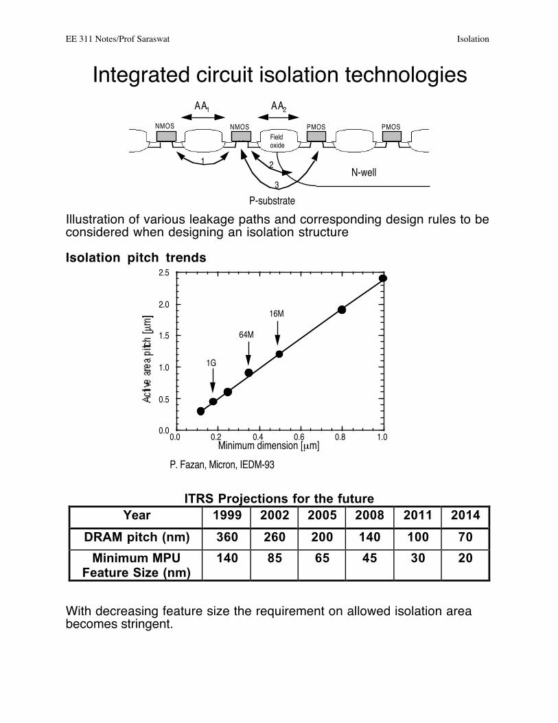
Integrated circuit isolation technologies
N+NMOS
N-well
P-substrate
1 2
3
AA1 AA2
NMOS PMOS PMOSField oxide
Illustration of various leakage paths and corresponding design rules to beconsidered when designing an isolation structure
Isolation pitch trends
0.0 0.2 0.4 0.6 0.8 1.0Minimum dimension [µm]
0.0
0.5
1.0
1.5
2.0
2.5
16M
64M
1G
Isolation pitch as a function of minimum dimension
P. Fazan, Micron, IEDM-93
ITRS Projections for the futureYear 1999 2002 2005 2008 2011 2014
DRAM pitch (nm) 360 260 200 140 100 70
Minimum MPUFeature Size (nm)
140 85 65 45 30 20
With decreasing feature size the requirement on allowed isolation areabecomes stringent.

EE 311 Notes/Prof Saraswat Isolation
2
Isolation Techniques
• Diffusion isolation with reverse biased diodes.o Historically used for bipolaro Currently used to isolate NMOS from PMOS through a well
• Oxide isolation
n+ p+
p-substrate
poly
− Used in early days of MOS− Field can’t be implanted for parasitic transistor Vt control− Step height is too much

EE 311 Notes/Prof Saraswat Isolation
3
• Local oxidation of silicon (LOCOS)− Main method used today in a variety of forms e. g., semi-recessed
LOCOS, fully-recessed LOCOS, SWAMI, poly-buffered LOCOS.
Grow SiO2, deposit Si3N4
BoronPattern,Field implant
Grow fieldoxide
Strip nitride, pad-oxide
Local Oxidation of Silicon (LOCOS) process sequence
− 0.6 µm pitch: LOCOS limit if thick (>300 nm) field oxides arerequired. 0.4 µm pitch with recessed LOCOS (200 nm field oxide)has been demonstrated (K. Shibahara et al. IEDM-94, p. 639). Belowthese dimensions LOCOS based technology may not be used.
• Trench isolation− Cutting edge technology today
Deep trench isolation
N-wellP-substrate
Shallow trench isolation

EE 311 Notes/Prof Saraswat Isolation
4
Fully-recessed and semi-recessed LOCOS
NitridePad oxide
Fully recessed LOCOS
Nitride Pad oxide
Semi-recessed LOCOSNitride
Field oxide
After field oxidation
After field oxidation
Illustration of the difference in shape and topography in a semi-recessedand fully-recessed LOCOS structure obtained by etching Si prior tooxidation.
TEM of Conventional semi-recessed LOCOS

EE 311 Notes/Prof Saraswat Isolation
5
2D effects in thermal oxidation of Si
Ref: Kao, McVittie, Nix, and Saraswat, ``2-D Thermal Oxidation of Silicon,'' IEEE Trans. Elec. Dev., May 1987.
Typical experimental result from Kao, et.al. Silicon wafers were plasma etched toproduce a variety of shaped structures including the cylinder illustrated in the topdrawing. These structures were oxidized and the oxide thickness was measured. Thedrawing at the right labels the structure shown experimentally on the left. The oxide isthinner on both concave and convex corners than it is on flat regions.

EE 311 Notes/Prof Saraswat Isolation
6
Typical experimental data after Kao. The oxide thickness is plotted versus the radius of curvatureof the structure being oxidized. For each temperature, about 500 nm of oxide was grown on a flatsurface (1/r = 0). These results are for H2O oxidations. Similar results were found for O2. Notethe retardation of the oxidation for sharp corners (more than a factor of 2 in some cases.
Several physical mechanisms are important in understanding these results.
2D Oxidant Diffusion: In corner regions and other shaped structures, oxidant transport to the Si/SiO2 interface is a 2D orperhaps even 3D transport problem. Since the oxide is amorphous, the diffusion coefficients of O2or H2O should not be direction dependent, but numerical techniques are generally required to solvethe diffusion equation in multiple dimensions.
Diffusion of oxidants in cylindrical structures. (a) shows the convex surface of a Si cylinder duringoxidation. Because of the wider exposure to the ambient, the concentration of the oxidant is higherin the convex case than it is for a flat surface. The opposite is true for the concave surface, such as ahole etched in the silicon as shown in (b).
EE 311 Notes/Prof Saraswat Isolation
7
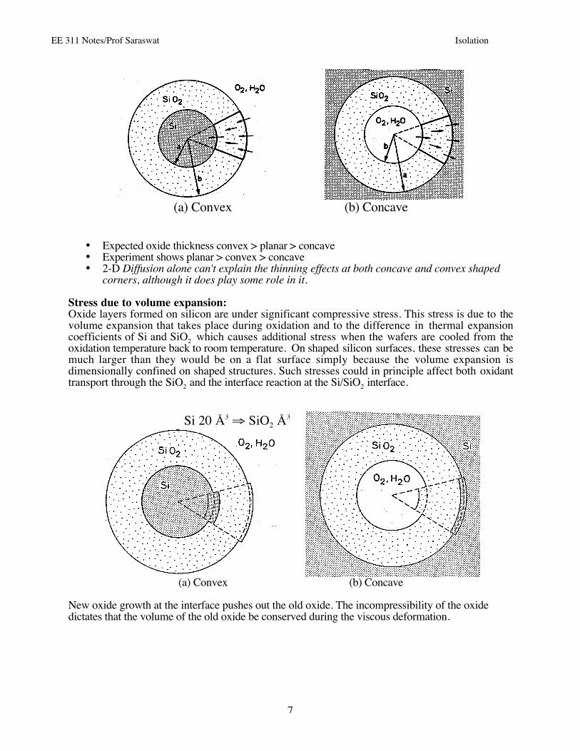
(a) Convex (b) Concave
• Expected oxide thickness convex > planar > concave• Experiment shows planar > convex > concave• 2-D Diffusion alone can't explain the thinning effects at both concave and convex shaped
corners, although it does play some role in it.
Stress due to volume expansion:Oxide layers formed on silicon are under significant compressive stress. This stress is due to thevolume expansion that takes place during oxidation and to the difference in thermal expansioncoefficients of Si and SiO2 which causes additional stress when the wafers are cooled from theoxidation temperature back to room temperature. On shaped silicon surfaces, these stresses can bemuch larger than they would be on a flat surface simply because the volume expansion isdimensionally confined on shaped structures. Such stresses could in principle affect both oxidanttransport through the SiO2 and the interface reaction at the Si/SiO2 interface.
(a) Convex (b) Concave
New oxide growth at the interface pushes out the old oxide. The incompressibility of the oxidedictates that the volume of the old oxide be conserved during the viscous deformation.
Si 20 Å3 ⇒ SiO2 Å3

EE 311 Notes/Prof Saraswat Isolation
8
Stress Effects from Non Planar Deformation
(a) Convex (b) ConcaveThere is a normal stress for both convex and concave surfaces; in the bulk of the oxide. Thepressure, is tensile for the convex structure in (a) and compressive for the concave structure in (b).
To model these stress effects, Kao et. al. suggested the following modifications to theparameters usually used in the linear parabolic model.
kS(stress) = kS exp −σnVRkT
exp −
σtVTkT
(1)
D(stress) = Dexp −P( ) VD( )kT
(2)
C*(stress) = C* exp −P( ) VS( )kT
(3)
where kS is the normal interface reaction rate, σn is the stress normal to the growing interface, σt isthe stress tangential to the growing interface, D is the normal oxidant diffusivity (at 1 Atm), C* isthe normal oxidant solubility and P is the hydrostatic pressure in the growing oxide. VR, VT, VD andVS are considered to be stress dependent activation volumes and should be regarded as fittingparameters. They are used in the SUPREM IV implementation of this model.
The final oxide parameter that is needed to calculate growth on shaped surfaces, is the oxideviscosity. SiO2 is a glass and can relax some of the stresses that build up during oxidation byviscoelastic flow. In fact, the stresses that can build up during oxidation are so large, that the oxideviscosity itself needs to be modeled as a function of stress. A relationship of the following formhas been found to produce good agreement with experiment
η(stress) = η(T) σSVC /2kTsinh σSVC /2kT( )
(4)
where η(T) is the stress free, temperature dependent, oxide viscosity, σs is the shear stress in theoxide, and VC is again a fitting parameter.
EE 311 Notes/Prof Saraswat Isolation
9
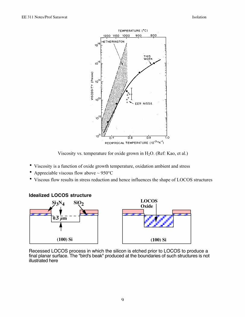
Viscosity vs. temperature for oxide grown in H2O. (Ref: Kao, et al.)
• Viscosity is a function of oxide growth temperature, oxidation ambient and stress
• Appreciable viscous flow above ~ 950°C
• Viscous flow results in stress reduction and hence influences the shape of LOCOS structures
Idealized LOCOS structureSi3N4 SiO2 LOCOS
Oxide
0.5 µm
(100) Si (100) Si
Recessed LOCOS process in which the silicon is etched prior to LOCOS to produce afinal planar surface. The "bird's beak" produced at the boundaries of such structures is notillustrated here

EE 311 Notes/Prof Saraswat Isolation
10
Realistic LOCOS structure
Simulation of a recessed LOCOS isolation structure using the ATHENA simulator. The initialstructure (top left) is formed by depositing a SiO2/Si3N4 structure followed by etching of this stackon the left side. The silicon is then etched to form a recessed oxide and the structure is oxidized for90 min at 1000˚C in H2O. The time evolution of the bird’s head shape during the oxidation isshown in the simulations. (Ref: Plummer’s book)
LOCOS structure parameters dependence on processparameters
Hbh2
Hbh1Hbb
Lbb
Parameters describing the bird’s beak in a semi-recessed LOCOS and thebird’s beak and bird’s head in a fully recessed LOCOS structure.

EE 311 Notes/Prof Saraswat Isolation
11
50 100 150 200 250Nitride thickness [nm]
100
200
300
400
50010 nm pad oxide15 nm pad oxide
Bird’s beak length dependence on nitride and pad oxide thickness in asemi-recessed LOCOS. The field oxide was grown at 1000˚C to athickness of approximately 600nm.
50 100 150 200 250Nitride thickness [nm]
50
100
150
200
25010 nm pad oxide15 nm pad oxide
Bird’s beak height dependence on nitride and pad oxide thickness in asemi-recessed LOCOS. The field oxide was grown at 1000˚C to athickness of approximately 600nm.

EE 311 Notes/Prof Saraswat Isolation
12
Problems in scaling of LOCOS type isolation structures
H2O
SiO2 NH3
Si
Si + NH3 Si3N4 + H2
Si3N4 + H2O SiO2 + NH3
The Kooi or “white ribbon” effect is due to the nitridation of the siliconsurface under the nitride mask edge. This can result in local thinning ofgate oxide. The local nitride can be removed by additional oxidation andetch.
Forces in Local Oxidation of Silicon
F4
F1
F2
F3
Schematic representation of forces acting on the silicon in a LOCOSstructure . F1: Intrinsic film stress F2: Bending stress F3: Field oxidegrowth F4: Thermal stress

EE 311 Notes/Prof Saraswat Isolation
13
0
10
Simulated LOCOS structures with contours of constant compressivestress (0, 10, 50, 100, and 500 MPa). No recess, 100 nm nitride
10 0
Simulated LOCOS structures with contours of constant compressivestress (0, 10, 50, 100, and 500 MPa). 150 nm recess, 200 nm nitride

EE 311 Notes/Prof Saraswat Isolation
14
100 120 140 160 180 200Nitride thickness [nm]
0
250
500
750
1000
1250
1500no recess100 nm recess150 nm recess
Average compressive stress in edge region along <111> for the different LOCOS isolationstructures.
Stress ↑ as nitride thickness ↑recess thickness ↑pad oxide thickness ↓oxidation temperature ↓
Example of an oxidation simulation showing the effects of including stress effects in oxidationusing the ATHENA simulator. A 20 nm SiO2 pad oxide is first grown and a 150 nm Si3N4 layer isthen deposited. The nitride is then etched on the left side of each structure. A 90 minute 1000˚CH2O oxidation was then performed. In the simulation on the left, no stress dependent parameters

EE 311 Notes/Prof Saraswat Isolation
15
were included in the simulation. Stress dependent parameters were included in the simulation onthe right. (Ref: Plummr’s Book)
Effect of stress on physical and electrical properties
Band gap narrowingWhen a crystal is mechanically deformed, the crystal symmetry and the lattice spacings arealtered and hence the energy bands change. The change in band gap can cause change in intrinsiccarrier concentration. This can result in increased junction leakage.
Crystal defect formationIf the stress exceeds the yield stress, defects can form resulting in further increase in leakage.
10 100 1000 10000Stress [MPa]
100
101
102
Hydrostatic[111]
Calculated influence of a pure hydrostatic and a uniaxial compressive stress along a <111>direction on the intrinsic carrier concentration.
EE 311 Notes/Prof Saraswat Isolation
16
0 250 500 750 1000 1250 1500
Average compressive stress [MPa]
0
100
200
300
400
DefectsNo defects
Gate overlap
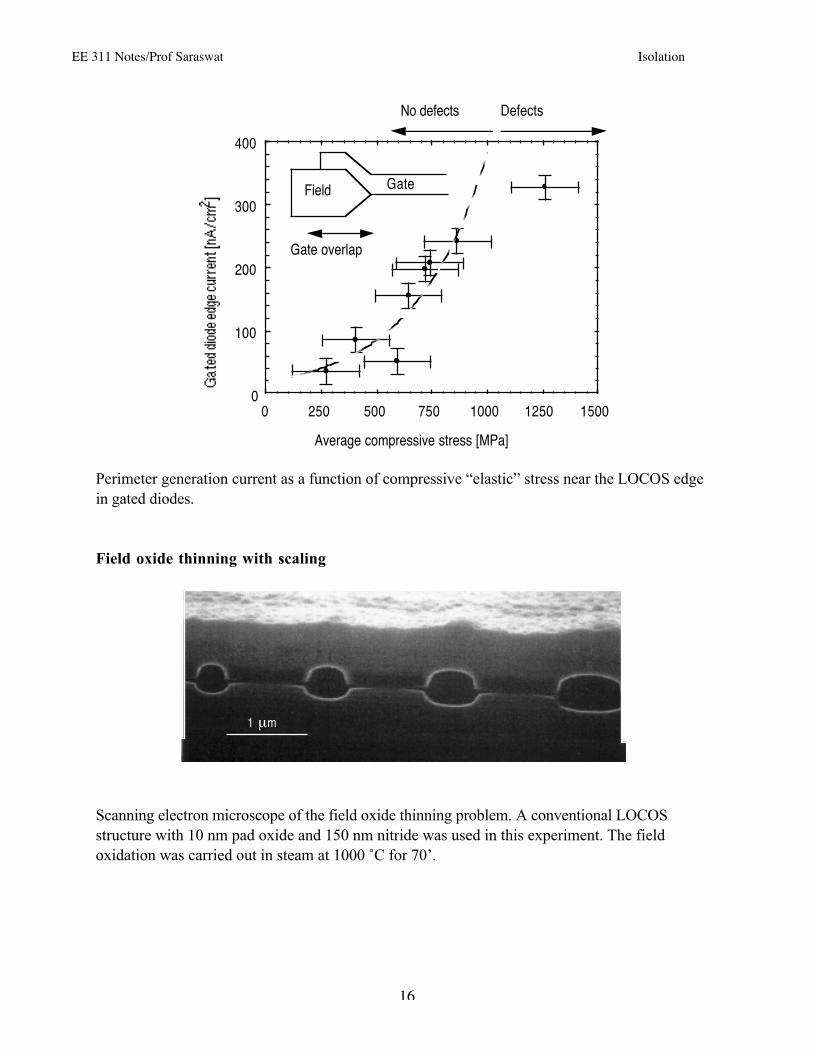
Field Gate
Perimeter generation current as a function of compressive “elastic” stress near the LOCOS edgein gated diodes.
Field oxide thinning with scaling
1 µm
Scanning electron microscope of the field oxide thinning problem. A conventional LOCOSstructure with 10 nm pad oxide and 150 nm nitride was used in this experiment. The fieldoxidation was carried out in steam at 1000 ˚C for 70’.
EE 311 Notes/Prof Saraswat Isolation
17
0.0 0.1 0.2 0.3 0.4 0.5 0.6 0.7 0.8 0.9 1.0Oxidation window width [µm]
0.5
0.6
0.7
0.8
0.9
1.0
LocosPoly-buffer LOCOS
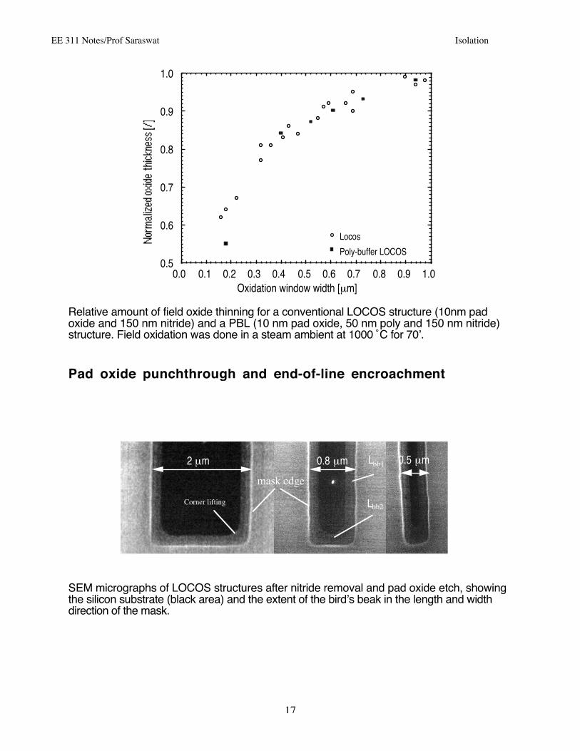
Relative amount of field oxide thinning for a conventional LOCOS structure (10nm padoxide and 150 nm nitride) and a PBL (10 nm pad oxide, 50 nm poly and 150 nm nitride)structure. Field oxidation was done in a steam ambient at 1000 ˚C for 70’.
Pad oxide punchthrough and end-of-line encroachment
2 µm 0.8 µm 0.5 µm
Lbb2
Lbb1
Corner lifting
mask edge
SEM micrographs of LOCOS structures after nitride removal and pad oxide etch, showingthe silicon substrate (black area) and the extent of the bird’s beak in the length and widthdirection of the mask.
EE 311 Notes/Prof Saraswat Isolation
18
0.0 0.5 1.0 1.5 2.0Distance [µm]
10-1110-1010-910-810-710-610-510-410-310-210-1100
1000 ˚C1100 ˚C
900 ˚C
Mask edge
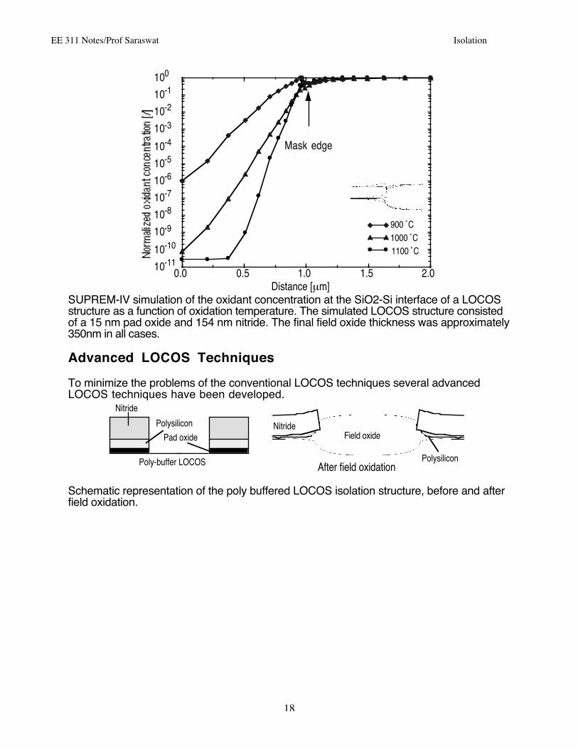
SUPREM-IV simulation of the oxidant concentration at the SiO2-Si interface of a LOCOSstructure as a function of oxidation temperature. The simulated LOCOS structure consistedof a 15 nm pad oxide and 154 nm nitride. The final field oxide thickness was approximately350nm in all cases.
Advanced LOCOS Techniques
To minimize the problems of the conventional LOCOS techniques several advancedLOCOS techniques have been developed.
Polysilicon
Poly-buffer LOCOS After field oxidation
Nitride
Pad oxide Field oxideNitride
Polysilicon
Schematic representation of the poly buffered LOCOS isolation structure, before and afterfield oxidation.

EE 311 Notes/Prof Saraswat Isolation
19
Simulation of an advanced isolation structure (the SWAMI process originally developed byHewlett-Packard), using the ATHENA simulator. The structure prior to oxidation is on the top left.This structure is formed by depositing an oxide followed by a thick Si3N4 layer, both of which areetched away on the left side. A silicon etch on the left side is then followed by a second oxide andnitride deposition. These layers are then etched away on the far left side, leaving the thin SiO2/Si3N4stack covering the sidewall of the silicon. A 450 min H2O oxidation at 1000˚C is then performedwhich results in the structure on the top right. An experimental structure fabricated with a similarprocess flow is shown on the bottom right. The stress levels in the SiO2 are shown at the end of theoxidation on the bottom left.
Nitride or poly spacerNitride
Pad-oxideRe-oxide
Nitride
Pad-oxideRe-oxide
Nitride or polysilicon
(a)
(b)
Schematic representation of nitride or poly spacer LOCOS (a) and Nitride-Clad or PELOX(b) before field oxidation

EE 311 Notes/Prof Saraswat Isolation
20
Trench Isolation
Deep trench isolation
N-wellP-substrate
Shallow trench isolation
Schematic representation of the shallow and deep trench structures for inter-device andinter-well isolation respectively. After etching and re-oxidizing the trench sidewalls, they arefilled with a deposited dielectric and planarized.
Fabrication sequence of of shallow trench isolation (STI)
EE 311 Notes/Prof Saraswat Isolation
21
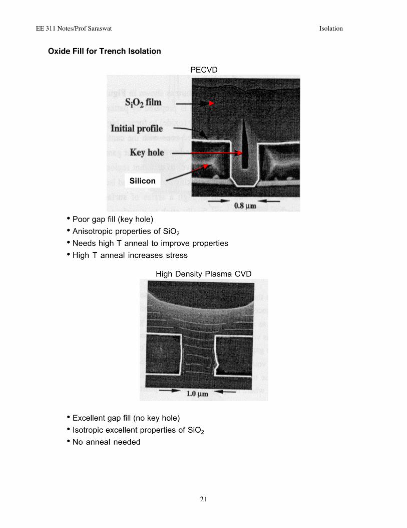
Oxide Fill for Trench Isolation
PECVD
Silicon
• Poor gap fill (key hole)
• Anisotropic properties of SiO2
• Needs high T anneal to improve properties
• High T anneal increases stress
High Density Plasma CVD
• Excellent gap fill (no key hole)
• Isotropic excellent properties of SiO2
• No anneal needed

EE 311 Notes/Prof Saraswat Isolation
22
Chemical-Mechanical Polishing (CMP) for Planarization
CMP Equipment
EE 311 Notes/Prof Saraswat Isolation
23
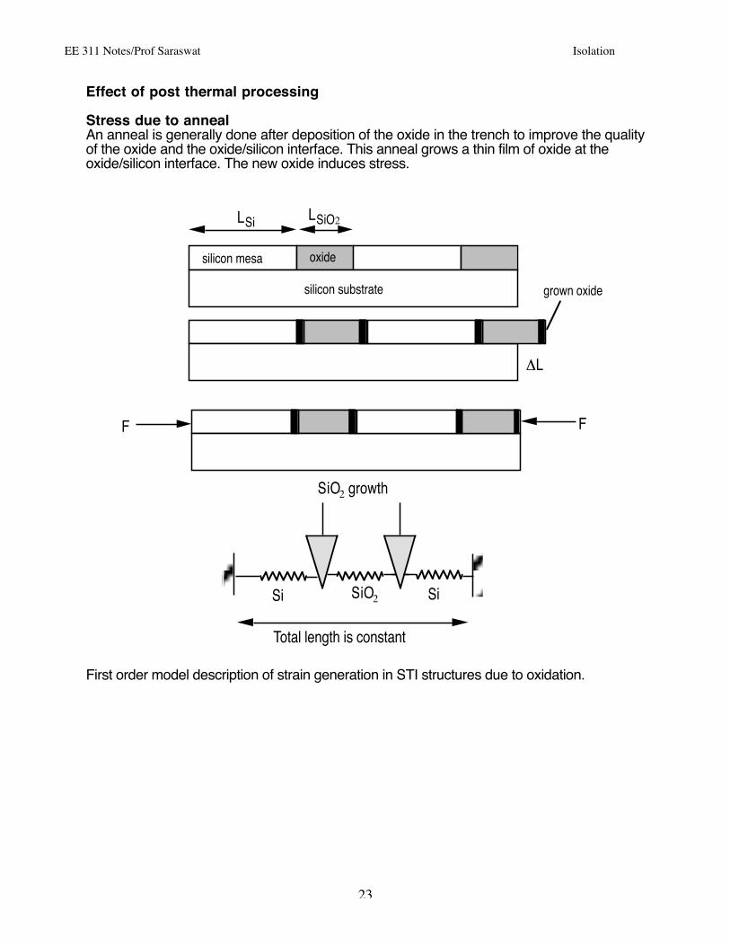
Effect of post thermal processing
Stress due to annealAn anneal is generally done after deposition of the oxide in the trench to improve the qualityof the oxide and the oxide/silicon interface. This anneal grows a thin film of oxide at theoxide/silicon interface. The new oxide induces stress.
Si SiO2 Si
SiO2 growth
ΔL
FF
LSi LSiO2
silicon mesa oxide
silicon substrate grown oxide
Total length is constant
First order model description of strain generation in STI structures due to oxidation.

EE 311 Notes/Prof Saraswat Isolation
24
1 100200400600800
100012001400160018002000
Active area length [µm]
900 ˚C
1000 ˚C
Increasing grown oxide thickness
Compressive stress in the silicon mesa as a function of active area length, LSi, oxidethickness (5, 10, 15, 20 nm) and oxidation temperature. The STI length, LSiO2 was 0.18 µmin all cases.
1 10Active area length [µm]
0200400600800
100012001400160018002000
Decreasing STI length (1-0.2 µm)
Compressive stress in the silicon mesa as a function of active area (mesa) and STI lengthfor an oxide of 10 nm grown at 1000 ˚C.
EE 311 Notes/Prof Saraswat Isolation
25
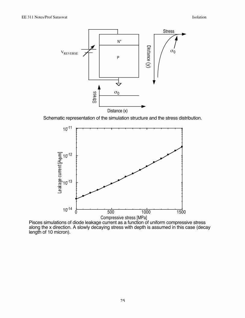
P
Stress
Distance (x)
σ0
σ0
N+
VREVERSE
Schematic representation of the simulation structure and the stress distribution.
0 500 1000 1500Compressive stress [MPa]
10-14
10-13
10-12
10-11
Pisces simulations of diode leakage current as a function of uniform compressive stressalong the x direction. A slowly decaying stress with depth is assumed in this case (decaylength of 10 micron).

EE 311 Notes/Prof Saraswat Isolation
26
1 10 100Active area pitch [µm]
100
101
102
103
900 ˚C
1000 ˚C
1100 ˚C
Stress-induced leakage increase, normalized to the stress free current as a function of STIactive device pitch and reoxidation temperature. Lower temperatures will result in higherstress and almost certainly lead to defect formation in scaled STI structures.
104 105 106 107 108 109 1010
Number of bits
10-14
10-13
10-12
10-11
10-10
Leakage current per cell as a function of DRAM generation. To reduce power requirementsassociated with refreshing data, long retention times (64-250 mSec.) necessitate lowerleakage currents (S. Asai, Hitachi)
EE 311 Notes/Prof Saraswat Isolation
27
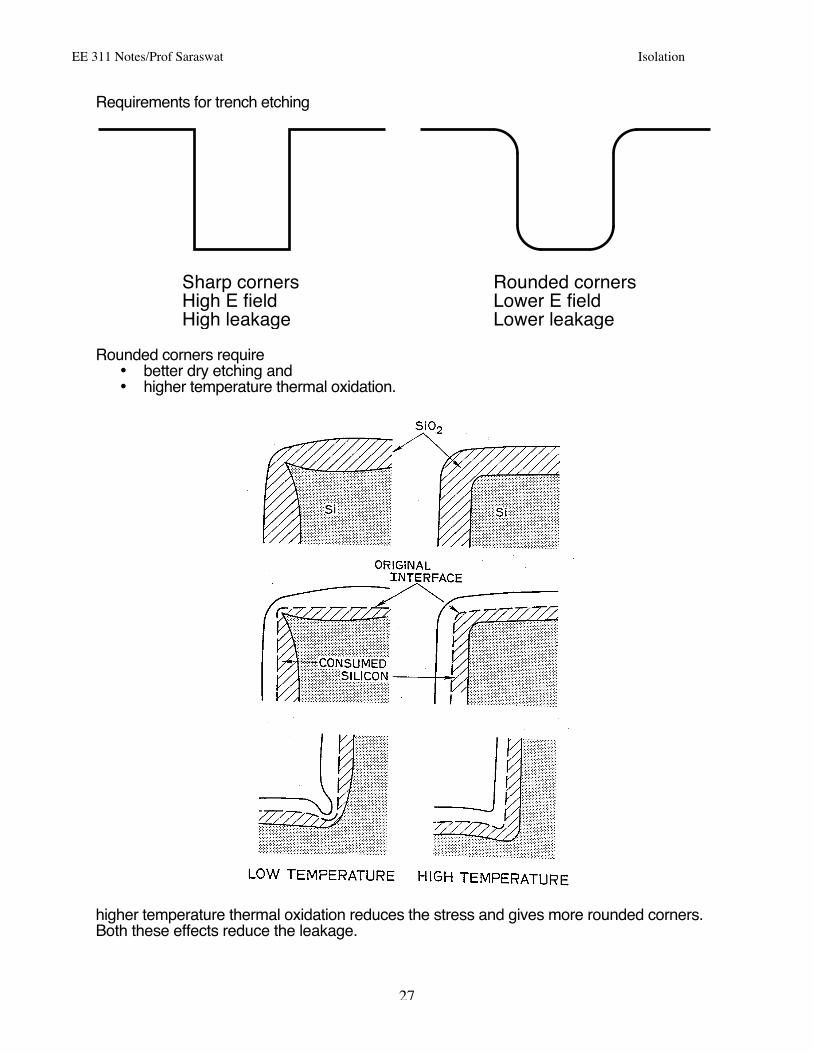
Requirements for trench etching
Sharp cornersHigh E fieldHigh leakage
Rounded cornersLower E fieldLower leakage
Rounded corners require• better dry etching and• higher temperature thermal oxidation.
higher temperature thermal oxidation reduces the stress and gives more rounded corners.Both these effects reduce the leakage.
EE 311 Notes/Prof Saraswat Isolation
28
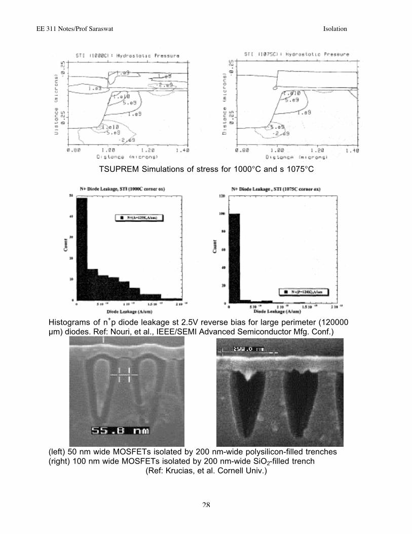
TSUPREM Simulations of stress for 1000°C and s 1075°C
Histograms of n+p diode leakage st 2.5V reverse bias for large perimeter (120000µm) diodes. Ref: Nouri, et al., IEEE/SEMI Advanced Semiconductor Mfg. Conf.)
(left) 50 nm wide MOSFETs isolated by 200 nm-wide polysilicon-filled trenches(right) 100 nm wide MOSFETs isolated by 200 nm-wide SiO2-filled trench
(Ref: Krucias, et al. Cornell Univ.)


