Universita degli Studi di Pavia
Facolta di Ingegneria
Dottorato di ricerca inMicroelettronica
XXII ciclo
Integrated magnetic sensor interfacecircuits and photovoltaic energy
harvester systems
Tutor:
Chiar.mo Prof. Piero Malcovati
Coordinatore del Corso di Dottorato:
Chiar.mo Prof. Rinaldo Castello
Tesi di Dottorato
di Ferri Massimo

Alle ambizioni

Contents
Introduction 1
1 Magnetic Sensor Interface Circuits 3
1.1 Introduction . . . . . . . . . . . . . . . . . . . . . . . . . . . . . 3
1.2 Magnetic Sensors . . . . . . . . . . . . . . . . . . . . . . . . . . 5
1.2.1 SQUID . . . . . . . . . . . . . . . . . . . . . . . . . . . 6
1.2.2 Search-coil . . . . . . . . . . . . . . . . . . . . . . . . . 6
1.2.3 Magneto-inductive sensor . . . . . . . . . . . . . . . . . 6
1.2.4 Magneto-resistance . . . . . . . . . . . . . . . . . . . . . 7
1.2.5 Hall sensor . . . . . . . . . . . . . . . . . . . . . . . . . 7
1.2.6 Fluxgate sensor . . . . . . . . . . . . . . . . . . . . . . . 9
1.3 Digital Compass System Characterization . . . . . . . . . . . . . 16
1.3.1 Magnetic field measurement system . . . . . . . . . . . . 18
1.3.2 Automated acquisition system . . . . . . . . . . . . . . . 25
1.3.3 Dedicated software . . . . . . . . . . . . . . . . . . . . . 30
1.3.4 Acquisition system optimization . . . . . . . . . . . . . . 32
1.3.5 Experimental results . . . . . . . . . . . . . . . . . . . . 34
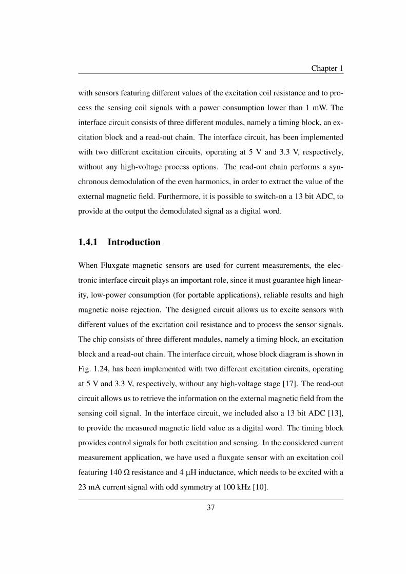
1.4 Re-Design of the Fluxgate Magnetic Sensor Interface Circuit . . . 36
1.4.1 Introduction . . . . . . . . . . . . . . . . . . . . . . . . . 37
1.4.2 Excitation circuits . . . . . . . . . . . . . . . . . . . . . 38
1.4.3 Read-out chain . . . . . . . . . . . . . . . . . . . . . . . 44
i
Contents
1.4.4 Experimental Results . . . . . . . . . . . . . . . . . . . . 59
2 Energy Harvesting 65
2.1 Introduction . . . . . . . . . . . . . . . . . . . . . . . . . . . . . 65
2.2 Micro Energy Harvesting . . . . . . . . . . . . . . . . . . . . . . 68
2.3 Photovoltaic Energy Harvesting Process . . . . . . . . . . . . . . 71
2.3.1 Optical absorption . . . . . . . . . . . . . . . . . . . . . 72
2.3.2 Solar cells . . . . . . . . . . . . . . . . . . . . . . . . . . 74
2.4 Integrated Micro-Solar Cell Structures for Harvesting Supplied
Microsystems in 0.35-µm CMOS Technology . . . . . . . . . . . 78
2.4.1 Solar cells characterization . . . . . . . . . . . . . . . . . 79
2.4.2 Power management system chip . . . . . . . . . . . . . . 84
2.4.3 Miniaturized solar cell model . . . . . . . . . . . . . . . 85
2.4.4 Ring oscillator and charge pump . . . . . . . . . . . . . . 87
2.4.5 Power monitoring circuit . . . . . . . . . . . . . . . . . . 88
2.4.6 Hysteresis comparator . . . . . . . . . . . . . . . . . . . 88
2.4.7 Voltage level shifter . . . . . . . . . . . . . . . . . . . . . 90
2.4.8 Voltage regulator . . . . . . . . . . . . . . . . . . . . . . 90
2.4.9 Storage capacitor sizing . . . . . . . . . . . . . . . . . . 92
2.4.10 Experimental results . . . . . . . . . . . . . . . . . . . . 93
2.5 Integrated Stabilized Photovoltaic Energy Harvester . . . . . . . . 95
2.5.1 Micro solar cells . . . . . . . . . . . . . . . . . . . . . . 96
2.5.2 Bandgap Reference Circuit . . . . . . . . . . . . . . . . . 98
2.5.3 LDO Circuit . . . . . . . . . . . . . . . . . . . . . . . . 101
2.5.4 Simulation Results . . . . . . . . . . . . . . . . . . . . . 103
2.5.5 Temperature Sensor . . . . . . . . . . . . . . . . . . . . 105
2.5.6 Experimental Results . . . . . . . . . . . . . . . . . . . . 105
2.5.7 Outlook . . . . . . . . . . . . . . . . . . . . . . . . . . . 107
ii

Contents
A PIC 16F877 Datasheet 111
Conclusions 113
iii


List of Figures
1.1 Classification of magnetic sensors . . . . . . . . . . . . . . . . . 5
1.2 Hall effect . . . . . . . . . . . . . . . . . . . . . . . . . . . . . . 8
1.3 Structure of a Fluxgate magnetic sensor . . . . . . . . . . . . . . 11
1.4 Effect of the magnetic field on the Fluxgate sensor output . . . . . 12
1.5 Structure of a planar Fluxgate magnetic sensor . . . . . . . . . . . 15
1.6 Structure of a planar Fluxgate sensor with an external magnetic field 16
1.7 Measurement and acquisition systems interaction . . . . . . . . . 17
1.8 Fluxgate sensor micro-photograph . . . . . . . . . . . . . . . . . 19
1.9 Block diagram of the integrated read-out circuit. . . . . . . . . . . 20
1.10 Effect of the magnetic field on the sensor output . . . . . . . . . . 22
1.11 Microphotograph of the integrated front-end circuit . . . . . . . . 24
1.12 Layout of the magnetic sensor interface circuit board . . . . . . . 24
1.13 Photograph of the magnetic sensor interface circuit board . . . . . 24
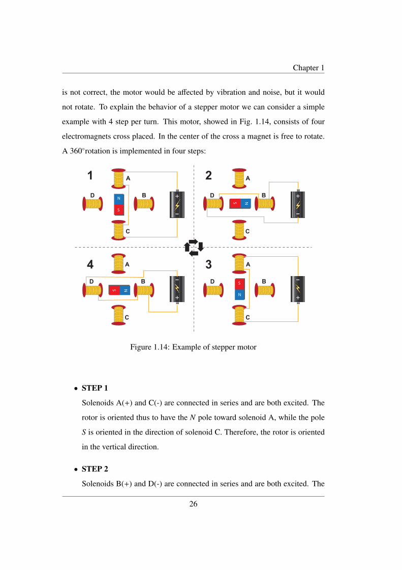
1.14 Example of stepper motor . . . . . . . . . . . . . . . . . . . . . . 26
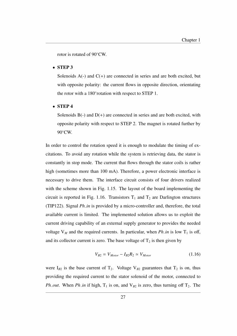
1.15 Driver adopted to excite a single solenoid of the stator . . . . . . . 28
1.16 Layout of the motor driver board . . . . . . . . . . . . . . . . . . 28
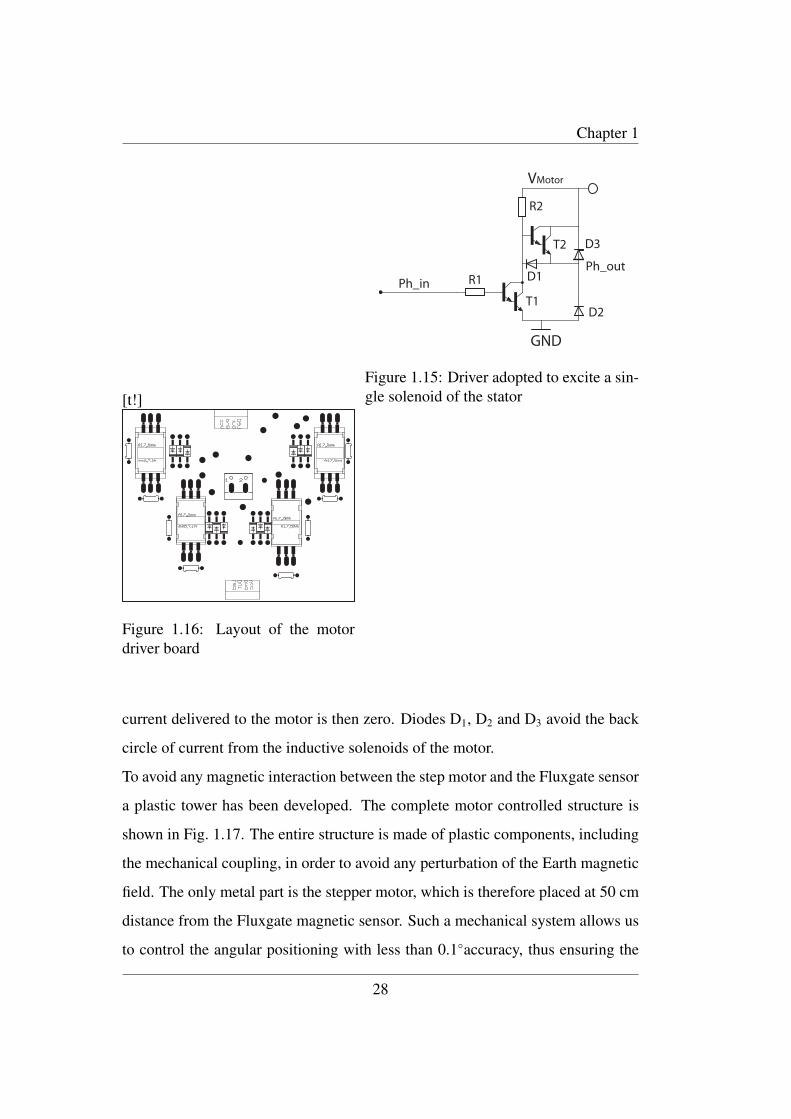
1.17 Plastic tower . . . . . . . . . . . . . . . . . . . . . . . . . . . . . 29
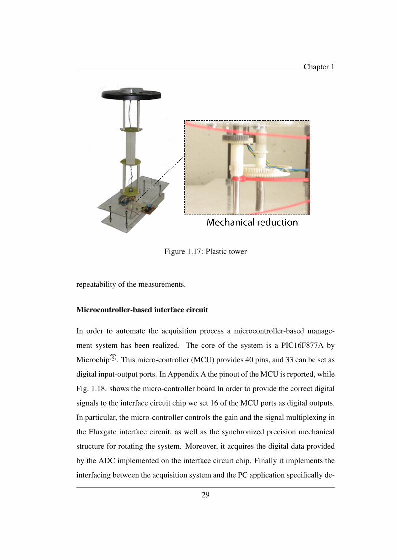
1.18 Board of the microcontroller-based interface circuit . . . . . . . . 30
1.19 Front panel of the software . . . . . . . . . . . . . . . . . . . . . 31
1.20 Angular accuracy as a function of the acquisition system evolution 33
v

Contents
1.21 Angular accuracy achieved with the automated acquisition system 34
1.22 Data acquired from the sensor over 360with the automated ac-
quisition system . . . . . . . . . . . . . . . . . . . . . . . . . . . 35
1.23 Linearity of the complete system . . . . . . . . . . . . . . . . . . 36
1.24 System block diagram . . . . . . . . . . . . . . . . . . . . . . . . 38
1.25 Schematic of the 3.3 V excitation circuit . . . . . . . . . . . . . . 39
1.26 Excitation current waveform obtained in simulation with the 3.3-
V excitation circuit . . . . . . . . . . . . . . . . . . . . . . . . . 39
1.27 Schematic of the 5-V excitation circuit . . . . . . . . . . . . . . . 40
1.28 Triangular waveform generator . . . . . . . . . . . . . . . . . . . 41
1.29 Waveform obtained in simulation at the output of the triangular
waveform generator . . . . . . . . . . . . . . . . . . . . . . . . . 42
1.30 Schematic of the voltage-driven current generator . . . . . . . . . 43
1.31 Current waveform delivered to the H-bridge obtained in simulation 44
1.32 Full H-Bridge circuit scheme . . . . . . . . . . . . . . . . . . . . 45
1.33 Current waveform delivered to the sensor obtained in simulation . 45
1.34 Block diagram of the read-out chain . . . . . . . . . . . . . . . . 46
1.35 Effect of the external magnetic field over the sensor . . . . . . . . 46
1.36 Charge injection . . . . . . . . . . . . . . . . . . . . . . . . . . . 48
1.37 Clock feed-through . . . . . . . . . . . . . . . . . . . . . . . . . 49
1.38 Schematic of the switches . . . . . . . . . . . . . . . . . . . . . . 49
1.39 Schematic of the operational amplifiers . . . . . . . . . . . . . . 50
1.40 Equivalent circuit of the operational amplifier . . . . . . . . . . . 51
1.41 Relation between gm and ID obtained with the circuit simulator . . 53
1.42 Bode diagram of the operational amplifiers used before the de-
modulator . . . . . . . . . . . . . . . . . . . . . . . . . . . . . . 54
vi

Contents
1.43 Bode diagram of the operational amplifiers used after the demod-
ulator . . . . . . . . . . . . . . . . . . . . . . . . . . . . . . . . 55
1.44 Instrumentation amplifier . . . . . . . . . . . . . . . . . . . . . . 56
1.45 Instrumentation amplifier transient response to an ideal Fluxgate
output signal . . . . . . . . . . . . . . . . . . . . . . . . . . . . . 57
1.46 Schematic of the Sallen-Key filter . . . . . . . . . . . . . . . . . 58
1.47 Frequency response of the Sallen-Key filter . . . . . . . . . . . . 59
1.48 Programmable gain amplifier . . . . . . . . . . . . . . . . . . . . 60
1.49 Programmable gain amplifier logic circuit scheme . . . . . . . . . 60
1.50 Microphotograph of the interface circuit chip . . . . . . . . . . . 61
1.51 Maximum relative linearity error of the system as a function of
the full-scale magnetic field . . . . . . . . . . . . . . . . . . . . . 62
1.52 Transfer characteristic of the system for a full-scale magnetic field
of 100 µT (±50 µT) . . . . . . . . . . . . . . . . . . . . . . . . . 62
1.53 Relative linearity error of the system for a full-scale magnetic field
of 100 µT (±50 µT) . . . . . . . . . . . . . . . . . . . . . . . . . 63
2.1 Trend of power dissipation in microprocessors design field . . . . 66
2.2 Optically generated electron-hole pair formation in a semiconductor 73
2.3 Photon intensity versus distance for two absorption coefficients . . 75
2.4 A p-n junction solar cell with resistive load . . . . . . . . . . . . 76
2.5 I-V characteristics of a p-n junction solar cell . . . . . . . . . . . 77
2.6 Maximum power rectangle of the solar cell I-V characteristics . . 78
2.7 Geometries and dimensions of the realized micro solar cells . . . . 79
2.8 Cross-section and equivalent circuit of realized solar structures . . 80
2.9 Short-circuit photo-generated current as a function of the incident
light power . . . . . . . . . . . . . . . . . . . . . . . . . . . . . 81
vii

Contents
2.10 Short-circuit photo-generated current as a function of the incident
light power with floating parasitic diode . . . . . . . . . . . . . . 82
2.11 Power curves of structure C: (Curve A) harvester contribution
with short-circuited parasitic diode, (Curve B) harvester contri-
bution with floating parasitic diode and (Curve C) sum of both
contributions . . . . . . . . . . . . . . . . . . . . . . . . . . . . 82
2.12 Block diagram of the proposed system . . . . . . . . . . . . . . . 84
2.13 Solar cell circuit model . . . . . . . . . . . . . . . . . . . . . . . 86
2.14 Schematic of the ring oscillator and of the charge pump . . . . . . 87
2.15 Schematic of the hysteresis comparator . . . . . . . . . . . . . . 89
2.16 Schematic of the voltage level shifter . . . . . . . . . . . . . . . . 91
2.17 Schematic of the linear voltage regulator . . . . . . . . . . . . . . 91
2.18 Simulation of the current flowing through the storage capacitor . . 93
2.19 Simulation of the voltage across the storage capacitor . . . . . . . 94
2.20 Microphotograph of the chip . . . . . . . . . . . . . . . . . . . . 94
2.21 Measurement of the voltage across the storage capacitor . . . . . . 95
2.22 Integrated micro solar cell structure . . . . . . . . . . . . . . . . 97
2.23 Schematic of the bandgap reference circuit . . . . . . . . . . . . . 99
2.24 Simulated temperature dependence of the bandgap reference voltage100
2.25 Schematic of the LDO circuit . . . . . . . . . . . . . . . . . . . . 101
2.26 Transient simulation of the system start-up with variable illumi-
nation . . . . . . . . . . . . . . . . . . . . . . . . . . . . . . . . 103
2.27 System output voltage as a function of temperature . . . . . . . . 104
2.28 Layout of the chip . . . . . . . . . . . . . . . . . . . . . . . . . . 104
2.29 Schematic of the complete system including the autonomous tem-
perature sensor . . . . . . . . . . . . . . . . . . . . . . . . . . . 106
2.30 Microphotograph of the chip . . . . . . . . . . . . . . . . . . . . 106
viii

Contents
2.31 Power curve of a reference photovoltaic cell . . . . . . . . . . . . 107
2.32 Power curve of the voltage regulator . . . . . . . . . . . . . . . . 107
2.33 Temperature sensor response . . . . . . . . . . . . . . . . . . . . 108
2.34 Summary of the performance of the system . . . . . . . . . . . . 108
ix


Introduction
The first part of the thesis focuses on the design of integrated magnetic sensor
interface circuits. Magnetic phenomena can represent an optimal information car-
rier in many applications. The first application considered is an electronic com-
pass based on a Fluxgate magnetic sensor. In particular we designed a reliable
measurement setup that allowed us to improve the previously obtained results of
50%. Indeed with a manual approach the maximum detectable angular accuracy
was 4 degrees, while with an automated approach it has been reduced to 1.5 de-
grees.
A new fluxgate magnetic sensor interface circuit has then been designed, to re-
alize a low-power current measurement system for portable applications. The
total power consumption has been drastically reduced with an improvement of the
linearity of the entire system. The circuit can provide a widely programmable ex-
citation current to the Fluxgate sensor and read-out the sensor signal with variable
gain. Moreover, the circuit provides digital output. All the design and implemen-
tation details are presented together with experimental results.
The second part of this thesis is focused on photovoltaic energy harvesting so-
lutions. In particular we realized two integrated microsystems. The first one is
photovoltaic power supply system for discrete-time applications. In particular we
realized a totally autonomous circuit that charges an external capacitor and moni-
tors the accumulated energy. When the energy is enough to supply an external or
on-chip system, the load is connected. When the capacitor is discharged the load
1

Introduction
is disconnected. This approach allows us to supply any kind of electronic device
that consumes more power than the power that the integrated micro solar cell can
provide. This solution has been realized in 0.35-µm standard CMOS technology.
The second energy harvester solution is a photovoltaic voltage regulator with an
autonomous temperature sensor. In particular the system provides a regulated 3.3-
V voltage supply and provides information about the temperature of the chip. The
system has been designed also for low level of illumination.
Both solutions are presented with experimental results.
2
Chapter 1
Magnetic Sensor Interface Circuits
In this chapter a short background information about magneticsensors is provided, with a detailed description of the considereddevices: the Fluxgate magnetic sensors. Moreover we will de-scribe the measurement setup that has been developed to charac-terize an integrated interface circuit previously realized. On thebasis of the obtained experimental results, a new version of the ispresented with the relative experimental results.
1.1 Introduction
Magnetic materials and their behavior are known since hundreds of years [1],
and their applications range have been drastically improved. At the beginning
they were available only as mechanical devices for navigation and orientation in
open spaces. The 1-1 compass is one of the oldest example. Recently to detect a
magnetic field it is possible to use both mechanical and electronic sensors. The
main advantage of the electronic sensors, which have been recently developed, is
that they can be integrated together with electronic interface circuits in the data
processing flow. This improves the embedding development trend, but introduces
3
Chapter 1
more complexity in the measurement setup design. There are several types of
magnetic sensors, but, basically, all of them, when detecting a magnetic field,
show a small variation of a physical property or of a parameter of the device.
The entity of this variation, which is related to the sensitivity of the sensor to the
applied magnetic field, makes the sensor itself suitable for a specific application
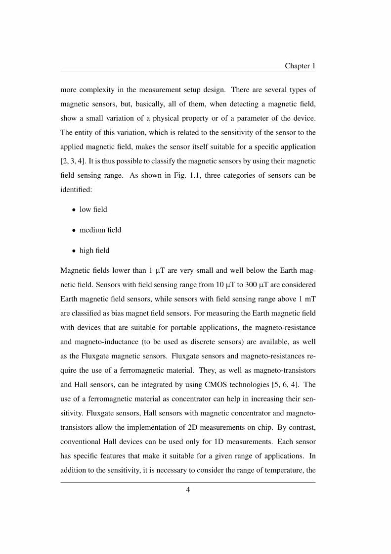
[2, 3, 4]. It is thus possible to classify the magnetic sensors by using their magnetic
field sensing range. As shown in Fig. 1.1, three categories of sensors can be
identified:
• low field
• medium field
• high field
Magnetic fields lower than 1 µT are very small and well below the Earth mag-
netic field. Sensors with field sensing range from 10 µT to 300 µT are considered
Earth magnetic field sensors, while sensors with field sensing range above 1 mT
are classified as bias magnet field sensors. For measuring the Earth magnetic field
with devices that are suitable for portable applications, the magneto-resistance
and magneto-inductance (to be used as discrete sensors) are available, as well
as the Fluxgate magnetic sensors. Fluxgate sensors and magneto-resistances re-
quire the use of a ferromagnetic material. They, as well as magneto-transistors
and Hall sensors, can be integrated by using CMOS technologies [5, 6, 4]. The
use of a ferromagnetic material as concentrator can help in increasing their sen-
sitivity. Fluxgate sensors, Hall sensors with magnetic concentrator and magneto-
transistors allow the implementation of 2D measurements on-chip. By contrast,
conventional Hall devices can be used only for 1D measurements. Each sensor
has specific features that make it suitable for a given range of applications. In
addition to the sensitivity, it is necessary to consider the range of temperature, the
4
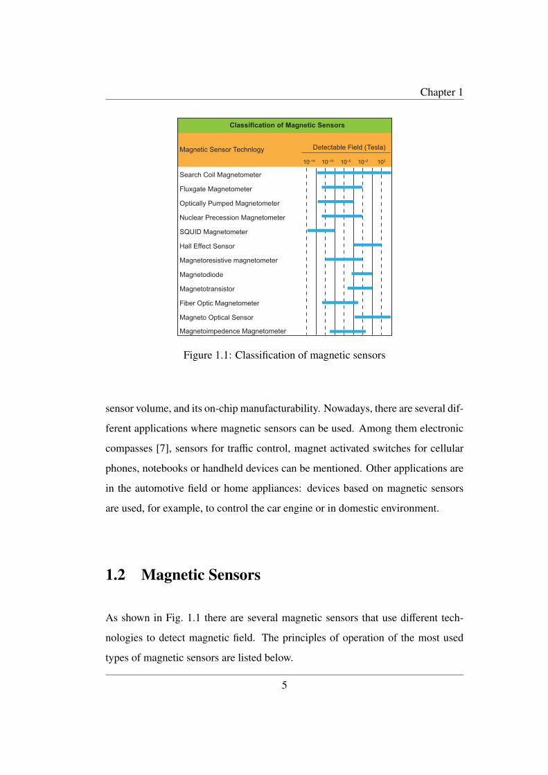
Chapter 1
Magnetic Sensor Technlogy
Classification of Magnetic Sensors
Detectable Field (Tesla)
10–14 10–10 10–5 10–2 102
Search Coil Magnetometer
Fluxgate Magnetometer
Optically Pumped Magnetometer
Nuclear Precession Magnetometer
SQUID Magnetometer
Hall Effect Sensor
Magnetoresistive magnetometer
Magnetodiode
Magnetotransistor
Fiber Optic Magnetometer
Magneto Optical Sensor
Magnetoimpedence Magnetometer
Figure 1.1: Classification of magnetic sensors
sensor volume, and its on-chip manufacturability. Nowadays, there are several dif-
ferent applications where magnetic sensors can be used. Among them electronic
compasses [7], sensors for traffic control, magnet activated switches for cellular
phones, notebooks or handheld devices can be mentioned. Other applications are
in the automotive field or home appliances: devices based on magnetic sensors
are used, for example, to control the car engine or in domestic environment.
1.2 Magnetic Sensors
As shown in Fig. 1.1 there are several magnetic sensors that use different tech-
nologies to detect magnetic field. The principles of operation of the most used
types of magnetic sensors are listed below.
5

Chapter 1
1.2.1 SQUID
The magnetic sensor with the highest sensitivity is the Superconducting Quantum
Interface Device (SQUID). Developed around 1962, it is able to detect magnetic
fields from few femto-Tesla to tens of Tesla. It is used in medical applications
since it can detect the human brain neuro-magnetic field (about few femtoTesla).
The main drawback of such a sensor is the low temperature of operation (about
4 K) needed to cool down the junction required to measure the current induced by
the magnetic field.
1.2.2 Search-coil
Search coils are based on the induction Faraday law, which establishes that the
induced voltage in a coil is proportional to the variation of the magnetic field
concatenated to the same coil. This voltage creates a current that is proportional
to the speed of the variation of the field itself. The sensitivity of the search-coil
depends on the properties of the magnetic material used, the area of the coils and
the number of coils used. The direct application of the Faraday law makes this
sensor not suitable for static or low-frequency fields.
1.2.3 Magneto-inductive sensor
fempto-Tesla The magneto-inductive sensor is a new type of magnetic sensor de-
veloped about twenty years ago. Nowadays it is one of the cheapest and most
used sensor thanks to its reliability. The magneto-inductive sensor is basically a
solenoid with magnetic material inside. If a current flows inside the solenoid, it
generates a magnetic field and an induced voltage. By linking this voltage to the
initial current it is possible to obtain the value of the inductance of the sensor. An
external magnetic field Hext changes the value of the magneto-inductance, since
it changes the value of the induced voltage by the sensed magnetic field. By em-
6

Chapter 1
ploying a circuit able to detect the value of the inductance, it is possible to derive
the value of an external magnetic field.
1.2.4 Magneto-resistance
Magneto-resistive sensors are based on the anisotropic magneto-resistance effect
(AMR) and have been developed in the last 30 years. Magneto-resistive sensors
exploit the fact that external fields H influences the electrical resistance ρ of cer-
tain ferromagnetic alloys. This solid-state magneto-resistive effect can be easily
realized by using a thin film technology. The specific resistance ρ of anisotropic
ferromagnetic metals depends on the angle θ between the internal magnetization
M and the current I, according to
ρ(θ) = ρp + (ρp − ρ‖)cos2(θ) (1.1)
where ρp and ρ‖ are the resistivities perpendicular and parallel to M. The quotient
(ρp − ρ‖)ρ
=∆ρ
ρ(1.2)
is called the magneto-resistive effect and may amount to several percent. Sensors
are always made of ferromagnetic thin films as this has two major advantages
over bulk material: the resistance is high and the anisotropy can be made uniaxial.
The ferromagnetic layer behaves like a single domain and has one distinguished
direction of magnetization in its plane called the easy axis (e.a.), which is the
direction of magnetization without external field influence.
1.2.5 Hall sensor
The Hall effect was discovered by Dr. Edwin Hall in 1879. Dr. Hall found that
when a magnet was placed so that its field was perpendicular to one face of a
thin rectangle of gold through which current was flowing, a difference in potential
7

Chapter 1
appeared at the opposite edges. He found that this voltage was proportional to the
current flowing through the conductor, and the flux density or magnetic induction
perpendicular to the conductor. When a current-carrying conductor is placed into
a magnetic field, a voltage will be generated perpendicular to both the current
and the field. This principle is known as the Hall effect. Figure 5.2-5 illustrates
the basic principle of the Hall effect. It shows a thin sheet of semiconducting
material (Hall element) through which a current flows. The output connections are
perpendicular to the direction of the current. When no magnetic field is present,
the current distribution is uniform and no potential difference is seen across the
output. When a perpendicular magnetic field is present a Lorentz force is exerted
on the current. This force disturbs the current distribution, resulting in a potential
difference (voltage) across the output. This voltage is the Hall voltage (VH). For
[ht]
Figure 1.2: Hall effect
the Lorentz’s law, a charged particle q moving inside the conductor in magnetic
8

Chapter 1
field B with a speed equal to vd, is subject to a force equal to:
F = q · vd × B (1.3)
where × is the vectorial product operator between vd and B.
In stationary condition this force is balanced by the induced electrical field gener-
ated from a charge redistribution, named Hall field HE. The integral of this field
along the conductor gives the Hall voltage VH. This voltage is equal to VH = EHW
in the case that B is uniform along the conductor, where W is the width. An elec-
tron placed inside the conductor is subject to a force equal to F = q ·EH. Using
equation 1.3, and considering vd = −Jx/q, where Jx is he current density, it results
q · EH = q · vd · B (1.4)
that means
EH = RH · Jx · B (1.5)
where RH is defined as the Hall coefficient. By considering parameter r that takes
into account the variation of speed of the carrier (+ for electrons or − for holes)
RH = ±r
q(1.6)
Hall voltage can be expressed as
VH = RHI · B
108t(1.7)
By using equation 1.7 it is possible to determine the type of carriers and the con-
centration. From this values and knowing the current, it is possible to obtain the
conductivity and the Hall mobility (µ = σ|RH |).
1.2.6 Fluxgate sensor
Fluxgate sensors are among the most used magnetometers thanks to their pos-
sibility to be integrated together with microelectronic circuits. Fluxgate magne-
tometers were first introduced in the 1930’s. Some development was for airborne
9

Chapter 1
magnetic surveys and for submarine detection, like Hall devices. They were fur-
ther developed for geomagnetic studies, for mineral prospecting and for magnetic
measurements in outer space. They have also been adapted and developed for
various detections and surveillance devices, both for civil and military use. De-
spite the advent of newer technologies for magnetic field measurements, Fluxgate
magnetometers continue to be used successfully in all of these areas, thanks to
their reliability, relative simplicity, and low cost. In the late 1950’s, the Flux-
gate was adapted to space magnetometer applications. Even as early as 1948, a
three-axis Fluxgate was used in an Aerobee sounding rocket to a peak altitude
of 112 km. The first satellite to carry a magnetometer of any type was Sputnik
3 which was launched in 1958 and carried a servo-oriented Fluxgate. Luniks 1
and 2 (Russian lunar probes), both launched in 1958, carried triaxial Fluxgates.
The USSR Venus probe launched in 1961 carried two single-axis Fluxgates. The
first American satellite to carry a Fluxgate was Earth orbiting Explorer 6 launched
in 1959. Some satellites or space probes carrying Fluxgate have included USSR
Mars probe, Nasa Explorer 12, 14 and 18, Mariner 2 (Venus) the USSR Earth-
orbit Electron 2 and Apollo 12, 14, 15 and 16. Nowadays, developments for this
sensor are expected in the solution based on CMOS technology for the coils and
CMOS compatible post-processing technology (i.e. sputtering) for the core de-
position. In this way, it is possible to realize micro-Fluxgates featuring very low
power consumption (in the order of few mW) and minimum silicon area. They
show some common point with magneto-inductances due essentially to their sim-
ilar structure. The basic structure of a Fluxgate sensor is shown in Fig. 1.3. The
sensor consists of a couple of coils: the first one provides the excitation [8] to
saturate the ferromagnetic material of the core (excitation coils). The second one
is used to read out the signal (sensing coils). These coils are wrapped around a
ferromagnetic core with an high magnetic permeability, in order to collect all the
10
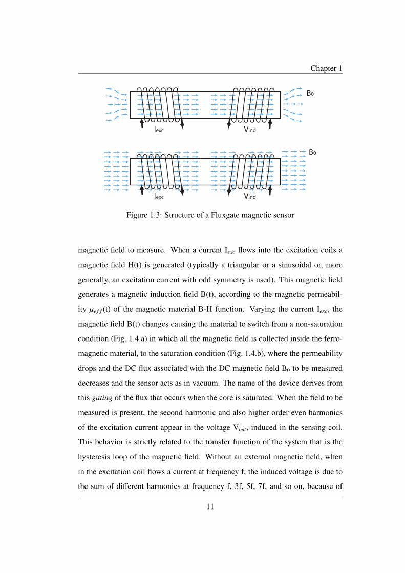
Chapter 1
Iexc Vind
B0
Iexc Vind
B0
Figure 1.3: Structure of a Fluxgate magnetic sensor
magnetic field to measure. When a current Iexc flows into the excitation coils a
magnetic field H(t) is generated (typically a triangular or a sinusoidal or, more
generally, an excitation current with odd symmetry is used). This magnetic field
generates a magnetic induction field B(t), according to the magnetic permeabil-
ity µe f f (t) of the magnetic material B-H function. Varying the current Iexc, the
magnetic field B(t) changes causing the material to switch from a non-saturation
condition (Fig. 1.4.a) in which all the magnetic field is collected inside the ferro-
magnetic material, to the saturation condition (Fig. 1.4.b), where the permeability
drops and the DC flux associated with the DC magnetic field B0 to be measured
decreases and the sensor acts as in vacuum. The name of the device derives from
this gating of the flux that occurs when the core is saturated. When the field to be
measured is present, the second harmonic and also higher order even harmonics
of the excitation current appear in the voltage Vout, induced in the sensing coil.
This behavior is strictly related to the transfer function of the system that is the
hysteresis loop of the magnetic field. Without an external magnetic field, when
in the excitation coil flows a current at frequency f, the induced voltage is due to
the sum of different harmonics at frequency f, 3f, 5f, 7f, and so on, because of
11
Chapter 1
Mag
netiz
ing
Fiel
d In
tens
ityM
agne
tizin
g Fl
uxIn
duce
d Vo
ltage
Sens
or O
utpu
t
Core A
Core B
t tt
t tt
t tt
t tt
Hext 1Hext 2
Wihout external field With external field >Hext 1 Hext 2
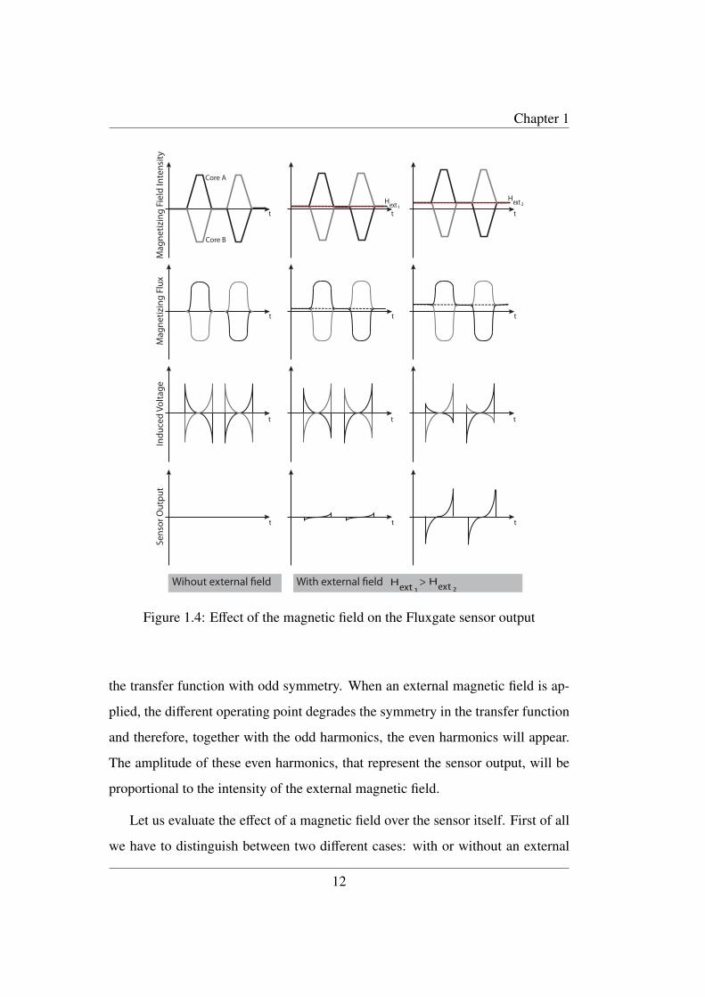
Figure 1.4: Effect of the magnetic field on the Fluxgate sensor output
the transfer function with odd symmetry. When an external magnetic field is ap-
plied, the different operating point degrades the symmetry in the transfer function
and therefore, together with the odd harmonics, the even harmonics will appear.
The amplitude of these even harmonics, that represent the sensor output, will be
proportional to the intensity of the external magnetic field.
Let us evaluate the effect of a magnetic field over the sensor itself. First of all
we have to distinguish between two different cases: with or without an external
12

Chapter 1
magnetic field Hext. If we assume the ferromagnetic material B-H characteristic
to be linear outside the saturation region with a constant value of µe f f , we obtain
B = µe f fµ0H (1.8)
where µ0 is the magnetic permeability of vacuum. If Hext = 0 (1st column in
Fig. 1.4), and a triangular excitation current with frequency f is used, a magnetic
field is generated, given by
H(t) = 4 · f ·Hm · t f or t ∈[−
14 f
Hs
Hm+
n
f,
14 f
Hs
Hm+
n
f
](1.9)
H(t) = −4 · f ·Hm · t f or t ∈[ 12 f−
14 f
Hs
Hm+
n
f,
12 f
+1
4 f
Hs
Hm+
n
f
](1.10)
where n is a integer. For the Faraday-Neumann law, the output voltage of the
sensor Vout is proportional to the time derivative of the magnetic flux through the
N sensing coils with area S.
Vout = −N ·dΦ
dt= −Nsens · A ·
dB
dt(1.11)
The time derivative of the induced magnetic field is equal to
dB
dt= 4 · µ · f ·Hm f or t ∈
[−
14 f
Bs
Bm+
n
f,
14 f
Bs
Bm+
n
f
](1.12)
dB
dt= −4 · f ·Hm · t f or t ∈
[−
14 f
Bs
Bm+
n + 12 f
,1
2 f+
14 f
Bs
Bm+
2n + 1f
](1.13)
Outside this time limits, the magnetic material is in the saturation condition and
thusdB
dt= 0. In this way Vout consists of equally spaced positive and negative
pulses, with amplitude equal to 4 ·N · S · µ · f ·Hm. If a positive external magnetic
field Hext is added, it changes the position and the length of the pulse, since it
changes the period of time in which the ferromagnetic material is in saturation
(2nd and 3rd column in Fig. 1.4). The negative pulse of Vout is shifted of the
13

Chapter 1
quantityHext
4 · f ·Hm, while the positive pulse is postponed of the same amount of
time. For a negative magnetic field the delays are the same but opposite in sign.
With a Fourier analysis the spectrum of the output induced voltage Vout consists
of odd harmonics if no external magnetic field is present, while second order and
higher order even harmonics appear in presence of external magnetic field.
For a sinusoidal excitation I = I0 · sin(2π f t) we obtain
Vind = −dΦ
dt= −Nsens · S ·
d
dt
[µ ·Nexc · I0 · (sin(2π · fexc · t)
l
](1.14)
where µ = µe f f · µ0 is the magnetic permeability, fexc is the excitation frequency,
Nsens the number of sensing coils, Nexc the number of excitation coils, l the length
of the excitation coils. The sensor sensitivity can be improved by maximizing the
induced voltage, and this can be done using the following solutions:
• by increasing the excitation frequency (fexc); however, an upper bound to
fexc is given by the cut-off frequency of the ferromagnetic material relative
permeability;
• by increasing the number of turns of the sensing coil (Nsens);
• by increasing the cross section of the ferromagnetic material (S), consider-
ing that a larger cross-section requires a larger current to saturate the ferro-
magnetic material and, hence, an increased power consumption.
The amplitude of the second harmonic is equal to:
Vout2 = 8 ·Nsens · S · µ · f ·Hext · sin(πHs
Hm
)· sin(4π f t) (1.15)
It is possible to notice that the amplitude is a linear function of the external mag-
netic field. The read out circuitry has to be able to detect the second order and
the even high order harmonics that carry information about the external magnetic
14
Chapter 1
field, rejecting the other harmonics of the spectrum.
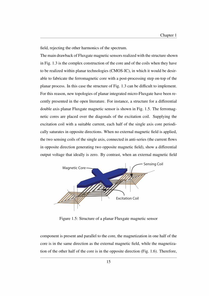
The main drawback of Fluxgate magnetic sensors realized with the structure shown
in Fig. 1.3 is the complex construction of the core and of the coils when they have
to be realized within planar technologies (CMOS-IC), in which it would be desir-
able to fabricate the ferromagnetic core with a post-processing step on-top of the
planar process. In this case the structure of Fig. 1.3 can be difficult to implement.
For this reason, new topologies of planar integrated micro-Fluxgate have been re-
cently presented in the open literature. For instance, a structure for a differential
double axis planar Fluxgate magnetic sensor is shown in Fig. 1.5. The ferromag-
netic cores are placed over the diagonals of the excitation coil. Supplying the
excitation coil with a suitable current, each half of the single axis core periodi-
cally saturates in opposite directions. When no external magnetic field is applied,
the two sensing coils of the single axis, connected in anti-series (the current flows
in opposite direction generating two opposite magnetic field), show a differential
output voltage that ideally is zero. By contrast, when an external magnetic field
Excitation Coil
Sensing CoilMagnetic Core
Figure 1.5: Structure of a planar Fluxgate magnetic sensor
component is present and parallel to the core, the magnetization in one half of the
core is in the same direction as the external magnetic field, while the magnetiza-
tion of the other half of the core is in the opposite direction (Fig. 1.6). Therefore,
15
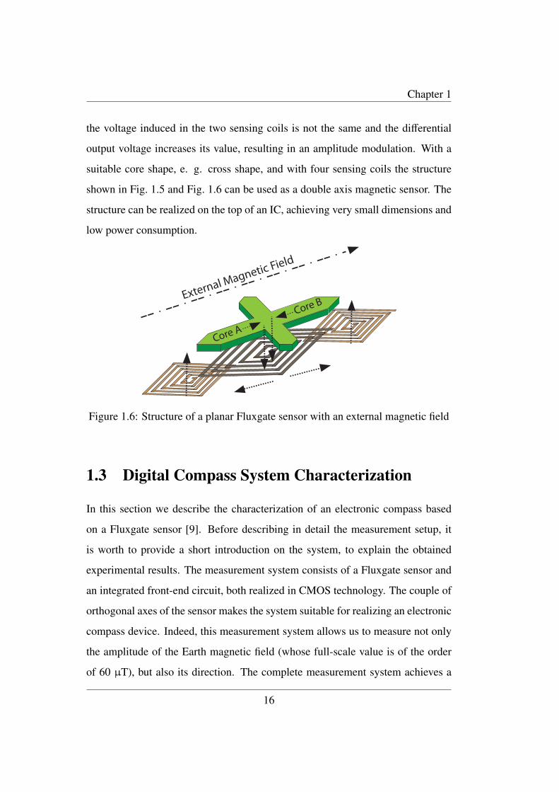
Chapter 1
the voltage induced in the two sensing coils is not the same and the differential
output voltage increases its value, resulting in an amplitude modulation. With a
suitable core shape, e. g. cross shape, and with four sensing coils the structure
shown in Fig. 1.5 and Fig. 1.6 can be used as a double axis magnetic sensor. The
structure can be realized on the top of an IC, achieving very small dimensions and
low power consumption.
Core A
Core BExternal Magnetic Field
Figure 1.6: Structure of a planar Fluxgate sensor with an external magnetic field
1.3 Digital Compass System Characterization
In this section we describe the characterization of an electronic compass based
on a Fluxgate sensor [9]. Before describing in detail the measurement setup, it
is worth to provide a short introduction on the system, to explain the obtained
experimental results. The measurement system consists of a Fluxgate sensor and
an integrated front-end circuit, both realized in CMOS technology. The couple of
orthogonal axes of the sensor makes the system suitable for realizing an electronic
compass device. Indeed, this measurement system allows us to measure not only
the amplitude of the Earth magnetic field (whose full-scale value is of the order
of 60 µT), but also its direction. The complete measurement system achieves a
16
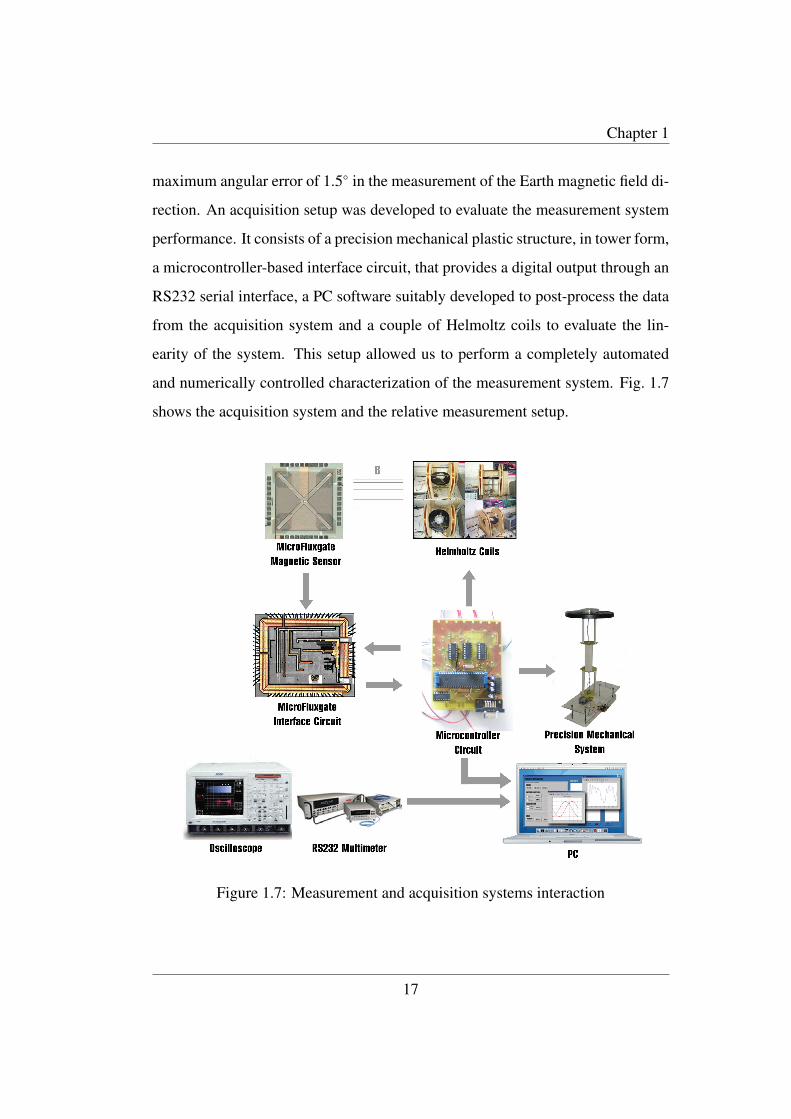
Chapter 1
maximum angular error of 1.5 in the measurement of the Earth magnetic field di-
rection. An acquisition setup was developed to evaluate the measurement system
performance. It consists of a precision mechanical plastic structure, in tower form,
a microcontroller-based interface circuit, that provides a digital output through an
RS232 serial interface, a PC software suitably developed to post-process the data
from the acquisition system and a couple of Helmoltz coils to evaluate the lin-
earity of the system. This setup allowed us to perform a completely automated
and numerically controlled characterization of the measurement system. Fig. 1.7
shows the acquisition system and the relative measurement setup.
Figure 1.7: Measurement and acquisition systems interaction
17

Chapter 1
1.3.1 Magnetic field measurement system
The Earth magnetic field measurement system consists of 2D planar fluxgate mag-
netic sensor and an integrated read-out circuit, for exciting the Fluxgate sensor and
reading-out the magnetic field magnitude in digital domain.
Fluxgate sensor
When realized with integrated circuit technologies, the three-dimensional geome-
try of a Fluxgate sensor evolves in a planar structure [10, 11], as shown in Fig. 1.5.
In this case, the excitation and sensing coils are implemented as spirals, realized
with two different metal layers, while the magnetic core is usually obtained with
a post processing of the silicon wafer. In Fig. 1.5 both magnetic axes are shown
but, for simplicity, only a pair of sensing coils are indicated. This structure is able
to detect a magnetic field coplanar with the structure itself, the output signal being
proportional to the projection of the field along the directions of the two cross arms
of the magnetic core. The integrated micro-Fluxgate used, whose photograph is
shown in Fig. 1.8, has been developed in a 0.5 µm CMOS process and the ferro-
magnetic core is realized as a post-processing step by dc-magnetron sputtering.
The obtained core features the good magnetic properties of the amorphous ferro-
magnetic material used as target (Vitrovac 6025 X), with a very small thickness
(about 1 µm). The thickness was chosen as a compromise between the sensitivity
of the device and the power consumption (the thicker the core, the higher is the
current required to bring it into saturation). The used technology includes copper
metal lines for the excitation coil and aluminum metal for the sensing coils. The
total area of the planar copper excitation coil (5.5 µm, 71 turns and 12 µm pitch
whose 8 µm metal width and 4 µm of spacing between two metals) is 1760 x 1760
µm2 and its resistance is about 123.4 Ω. The total area for the aluminium sensing
coils (1 µm thickness, 66 turns, 3 µm pitch with 1.4 µm metal width and 1.6 µm
18
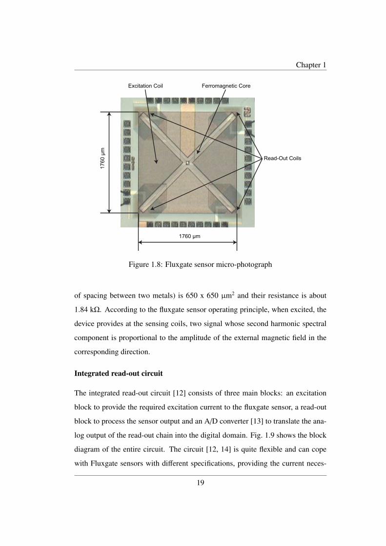
Chapter 1
Ferromagnetic CoreExcitation Coil
1760 µm
Read-Out Coils
1760
µm
Figure 1.8: Fluxgate sensor micro-photograph
of spacing between two metals) is 650 x 650 µm2 and their resistance is about
1.84 kΩ. According to the fluxgate sensor operating principle, when excited, the
device provides at the sensing coils, two signal whose second harmonic spectral
component is proportional to the amplitude of the external magnetic field in the
corresponding direction.
Integrated read-out circuit
The integrated read-out circuit [12] consists of three main blocks: an excitation
block to provide the required excitation current to the fluxgate sensor, a read-out
block to process the sensor output and an A/D converter [13] to translate the ana-
log output of the read-out chain into the digital domain. Fig. 1.9 shows the block
diagram of the entire circuit. The circuit [12, 14] is quite flexible and can cope
with Fluxgate sensors with different specifications, providing the current neces-
19
Chapter 1
-
+VIN -
+-
+
Micro FluxgateMagnetic
Sensor
Ibias
High VoltageStage (25 V)
Low VoltageStage (3.3 V)
Excitation
Micro FluxgateMagnetic
Sensor
X10V1
+VD VM VO
V1–
V+
V–
AMIXERDifferenceAmplifier
X6
X10 AMIXERDifferenceAmplifier
X6
MULTIPLEXER
IncrementalADC
Read-Out
Sallen-Key Filter
Sallen-Key Filter
b2 b1
b2 b1
b0
Figure 1.9: Block diagram of the integrated read-out circuit.
sary for their correct operation and reading-out the output voltage. This has two
main consequences: first the excitation circuit output stage had to be implemented
with a high voltage technology, in order to supply the required current (in the tens
of milliampere range) into a wide range of coil resistances (with a worst case of
280 Ω); second the read-out block needs to have a programmable gain to accom-
modate the various amplitudes of the sensor output signals.
The excitation circuit consists of two different blocks, with two different power
supplies: the first one is the low-voltage block, with a supply voltage equal to
3.3 V, while the second, realized with high-voltage transistors, uses a supply volt-
age up to 25 V. A linear, class-AB output stage has been used in order to minimize
the distortion of the excitation current, and allow the interface circuit to excite sen-
sors with different coil impedance. The first block generates a square wave with a
frequency equal to 100 kHz and programmable output amplitude, which is then in-
20
Chapter 1
tegrated, in order to obtain a triangular waveform, centered around half of the 3.3-
V supply voltage. The excitation of the sensor with a triangular current waveform
represents a trade-off between the low-noise performance of solutions based on
sinusoidal excitation and the simple implementation of solutions based on pulsed
excitation [15]. The second block consists of a high voltage mirrored operational
amplifier with low-impedance output stage, which receives the triangular wave-
form at the input and, through a resistive feedback produces a triangular current
at the output. A mirrored amplifier allows us to achieve the maximum swing at
the output terminal. The class-AB output stage of the amplifier is designed to
provide all the current required by the sensor. A decoupling stage between the
low-voltage and the high-voltage blocks is necessary to level-shift the triangular
wave produced by the low-voltage block around half of the high-voltage power
supply.
In order to ensure proper timing for the excitation and read-out blocks, the whole
circuit is driven by a clock at 400 kHz. This clock is internally divided by a cas-
cade of flip-flops. The outputs of this timing circuit are two signals: a 100 kHz
square wave signal with its complementary output, that is used to drive the excita-
tion block, and a 200 kHz square wave signal used to drive the read-out block and
to realize the second harmonic demodulation, needed to measure the sensor out-
put. By using a 400 kHz master clock a duty cycle of 50% on both the 100 kHz
and the 200 kHz output waveform can be ensured. A duty cycle different from
50%, indeed, could compromise the demodulation of the signals produced by the
sensing coils and, therefore, it has to be avoided.
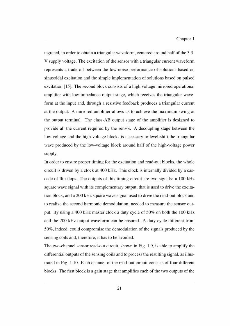
The two-channel sensor read-out circuit, shown in Fig. 1.9, is able to amplify the
differential outputs of the sensing coils and to process the resulting signal, as illus-
trated in Fig. 1.10. Each channel of the read-out circuit consists of four different
blocks. The first block is a gain stage that amplifies each of the two outputs of the
21
Chapter 1
Mag
netiz
ing
Fiel
d In
tens
ityCore A
Core B
t ttHext 1
Hext 2
VM
t tt
VM VM
t tt
Vo Vo Vo
t tt
Vo Vo Vo
X10
Volta
ge o
utpu
t
t tt
V1+
V1+V1+
V1-V1
-V1-
Indu
ced
Volta
ge
t tt
V+
V-
V+
V-
V+
V-
Figure 1.10: Effect of the magnetic field on the sensor output
22
Chapter 1
sensing coils (V+ and V−) by a factor of ten. In the second block the difference be-
tween the two outputs of the first block (V+1 and V−1 ) is amplified again by a factor
of six (VD) and demodulated (VM), to translate the second and higher order even
harmonics, which contain information on the magnetic field, down to dc. In order
to ensure the correct demodulation of the sensor signal and to avoid problems due
to the possible asynchronicity between the clock and the output itself, a quadra-
ture demodulation was implemented. Using this technique and adding together
the contribution of the two orthogonal signals, it is possible to avoid errors due
to timing misalignments between the read-out clock and the output of the sensor.
The demodulation of the signal is performed with the 200 kHz clock generated
by the timing circuit. The third block is a second order Sallen-Key low-pass filter
that removes all the high frequency components resulting from the demodulation
and returns a dc value that is proportional to the magnetic field. The difference
between this output voltage and the analog ground is the amplified with a digitally
programmable gain (from 1 to 100 with digital signals b1 and b2) in the last block
(Vo). For all the blocks we used a conventional two-stages operational amplifiers.
The dc output of the read-out chain is finally processed by a 13-bit incremen-
tal ADC, and delivered in digital form to the output interface. We used a single
ADC with a multiplexer, driven by digital signal b0 for both the read-out channels.
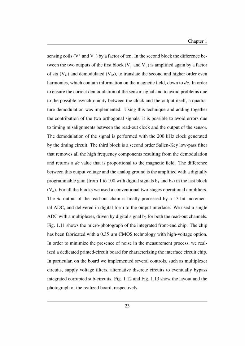
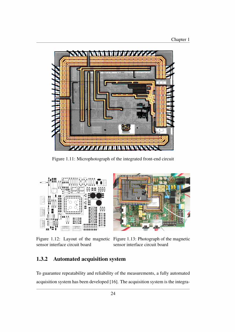
Fig. 1.11 shows the micro-photograph of the integrated front-end chip. The chip
has been fabricated with a 0.35 µm CMOS technology with high-voltage option.
In order to minimize the presence of noise in the measurement process, we real-
ized a dedicated printed-circuit board for characterizing the interface circuit chip.
In particular, on the board we implemented several controls, such as multiplexer
circuits, supply voltage filters, alternative discrete circuits to eventually bypass
integrated corrupted sub-circuits. Fig. 1.12 and Fig. 1.13 show the layout and the
photograph of the realized board, respectively.
23
Chapter 1
Figure 1.11: Microphotograph of the integrated front-end circuit
Figure 1.12: Layout of the magneticsensor interface circuit board
Figure 1.13: Photograph of the magneticsensor interface circuit board
1.3.2 Automated acquisition system
To guarantee repeatability and reliability of the measurements, a fully automated
acquisition system has been developed [16]. The acquisition system is the integra-
24

Chapter 1
tion between mechanical and electronic subsystems. To make the measurement
process completely automated, a microcontroller-based interface circuit was de-
veloped, together with a plastic rotating tower and a dedicated PC software. The
automation of the process has allowed to improve the reliability of the measured
data more that 50% with respect to a manual setup system.
Stepper motor control and precision rotating plastic tower
The positioning precision of the sensor in the Earth magnetic field is the most crit-
ical requirement in the design of the acquisition setup. The main contribution to
the angular error obtained in previous manual approaches [12] is closely related
to the mechanism of orientation of the sensor with respect to the direction of the
external magnetic field. In order to ensure a high level of precision, the manual
positioning has been substituted with an automated and numerically controlled
process. In particular, we adopted a stepper motor, driven by an appropriate elec-
tronic interface. Stepper motors, differently than other motors, turn due to a series
of electrical pulses to the motor windings. Each pulse rotates the rotor by an ex-
act angle. These pulses are called ”steps”, hence the name ”stepper motor”. The
rotation angle per pulse is set by the motor manufacturing and it is provided in the
data-sheet of the motor. They can range from a fraction of a degree (i. e., 0.10)
for ultra-fine movements, to larger steps (i. e. 62.5). The motor that we used was
retrieved from an inkjet printer and provides 0.5 degree/pulse (dpp). In order to
obtain a finest precision, a mechanical reduction has been introduced, thus allow-
ing us to obtain a precision well below 0.1.
Stepper motors consist of a permanent magnet rotating shaft, called the rotor, and
electromagnets on the stationary portion that surrounds the motor, called the sta-
tor. In order to make the rotor move, the electromagnets of the stator must be
excited with a proper sequence, composed of four steps. Whenever the sequence
25
Chapter 1
is not correct, the motor would be affected by vibration and noise, but it would
not rotate. To explain the behavior of a stepper motor we can consider a simple
example with 4 step per turn. This motor, showed in Fig. 1.14, consists of four
electromagnets cross placed. In the center of the cross a magnet is free to rotate.
A 360rotation is implemented in four steps:
N
S
N
S
+
-
NS NS
+
-
N
S
N
S
+
-
NS NS+
-
1 2
34
A
B
C
D
A
B
C
D
A
B
C
D
A
B
C
D
Figure 1.14: Example of stepper motor
• STEP 1
Solenoids A(+) and C(-) are connected in series and are both excited. The
rotor is oriented thus to have the N pole toward solenoid A, while the pole
S is oriented in the direction of solenoid C. Therefore, the rotor is oriented
in the vertical direction.
• STEP 2
Solenoids B(+) and D(-) are connected in series and are both excited. The
26
Chapter 1
rotor is rotated of 90CW.
• STEP 3
Solenoids A(-) and C(+) are connected in series and are both excited, but
with opposite polarity: the current flows in opposite direction, orientating
the rotor with a 180rotation with respect to STEP 1.
• STEP 4
Solenoids B(-) and D(+) are connected in series and are both excited, with
opposite polarity with respect to STEP 2. The magnet is rotated further by
90CW.
In order to control the rotation speed it is enough to modulate the timing of ex-
citations. To avoid any rotation while the system is retrieving data, the stator is
constantly in stop mode. The current that flows through the stator coils is rather
high (sometimes more than 100 mA). Therefore, a power electronic interface is
necessary to drive them. The interface circuit consists of four drivers realized
with the scheme shown in Fig. 1.15. The layout of the board implementing the
circuit is reported in Fig. 1.16. Transistors T1 and T2 are Darlington structures
(TIP122). Signal Ph in is provided by a micro-controller and, therefore, the total
available current is limited. The implemented solution allows us to exploit the
current driving capability of an external supply generator to provides the needed
voltage VM and the required currents. In particular, when Ph in is low T1 is off,
and its collector current is zero. The base voltage of T2 is then given by
VB2 = VMotor − IB2R2 ' VMotor (1.16)
were IB2 is the base current of T2. Voltage VB2 guarantees that T2 is on, thus
providing the required current to the stator solenoid of the motor, connected to
Ph out. When Ph in if high, T1 is on, and VB2 is zero, thus turning off T2. The
27
Chapter 1
[t!]
VMotor
GND
Ph_inPh_out
T1
T2
R1
R2
D1
D2
D3
Figure 1.15: Driver adopted to excite a sin-gle solenoid of the stator
Figure 1.16: Layout of the motordriver board
current delivered to the motor is then zero. Diodes D1, D2 and D3 avoid the back
circle of current from the inductive solenoids of the motor.
To avoid any magnetic interaction between the step motor and the Fluxgate sensor
a plastic tower has been developed. The complete motor controlled structure is
shown in Fig. 1.17. The entire structure is made of plastic components, including
the mechanical coupling, in order to avoid any perturbation of the Earth magnetic
field. The only metal part is the stepper motor, which is therefore placed at 50 cm
distance from the Fluxgate magnetic sensor. Such a mechanical system allows us
to control the angular positioning with less than 0.1accuracy, thus ensuring the
28
Chapter 1
Figure 1.17: Plastic tower
repeatability of the measurements.
Microcontroller-based interface circuit
In order to automate the acquisition process a microcontroller-based manage-
ment system has been realized. The core of the system is a PIC16F877A by
Microchip R©. This micro-controller (MCU) provides 40 pins, and 33 can be set as
digital input-output ports. In Appendix A the pinout of the MCU is reported, while
Fig. 1.18. shows the micro-controller board In order to provide the correct digital
signals to the interface circuit chip we set 16 of the MCU ports as digital outputs.
In particular, the micro-controller controls the gain and the signal multiplexing in
the Fluxgate interface circuit, as well as the synchronized precision mechanical
structure for rotating the system. Moreover, it acquires the digital data provided
by the ADC implemented on the interface circuit chip. Finally it implements the
interfacing between the acquisition system and the PC application specifically de-
29
Chapter 1
Figure 1.18: Board of the microcontroller-based interface circuit
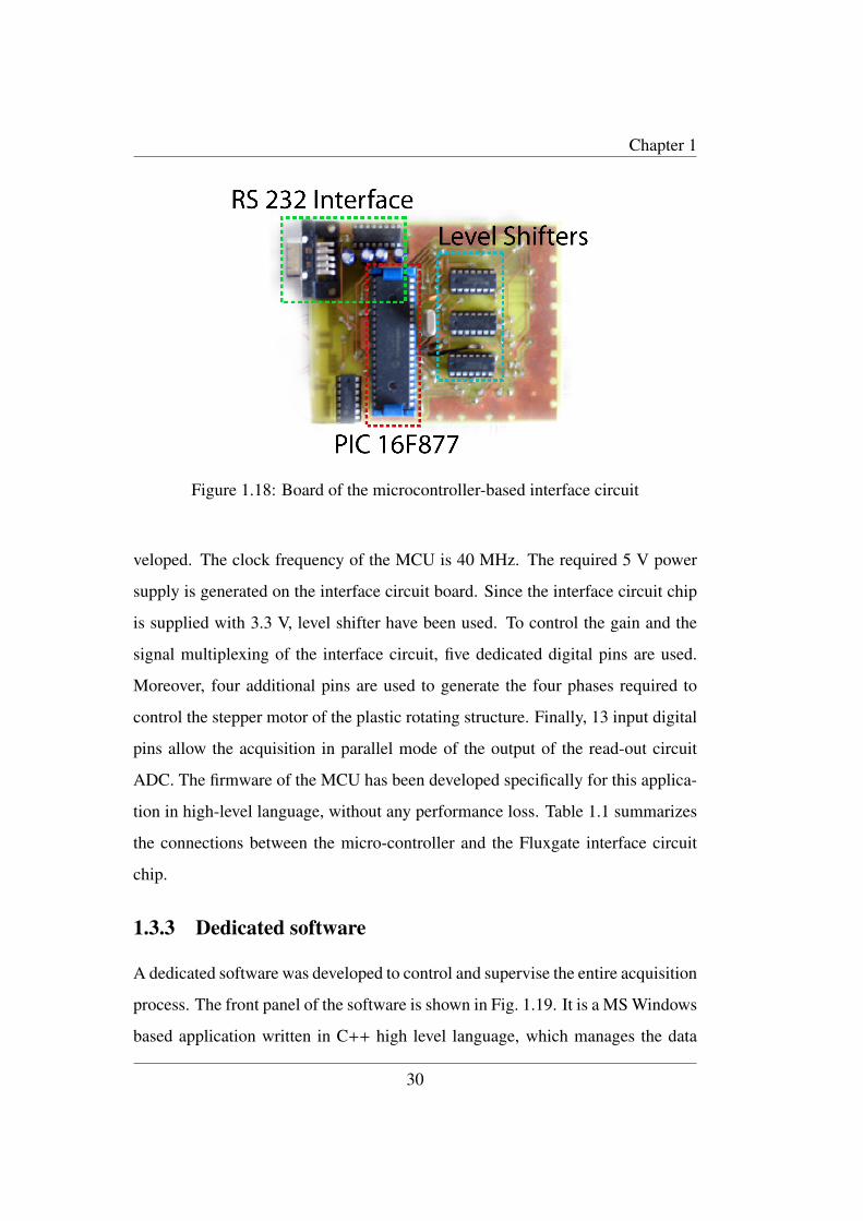
veloped. The clock frequency of the MCU is 40 MHz. The required 5 V power
supply is generated on the interface circuit board. Since the interface circuit chip
is supplied with 3.3 V, level shifter have been used. To control the gain and the
signal multiplexing of the interface circuit, five dedicated digital pins are used.
Moreover, four additional pins are used to generate the four phases required to
control the stepper motor of the plastic rotating structure. Finally, 13 input digital
pins allow the acquisition in parallel mode of the output of the read-out circuit
ADC. The firmware of the MCU has been developed specifically for this applica-
tion in high-level language, without any performance loss. Table 1.1 summarizes
the connections between the micro-controller and the Fluxgate interface circuit
chip.
1.3.3 Dedicated software
A dedicated software was developed to control and supervise the entire acquisition
process. The front panel of the software is shown in Fig. 1.19. It is a MS Windows
based application written in C++ high level language, which manages the data
30
Chapter 1
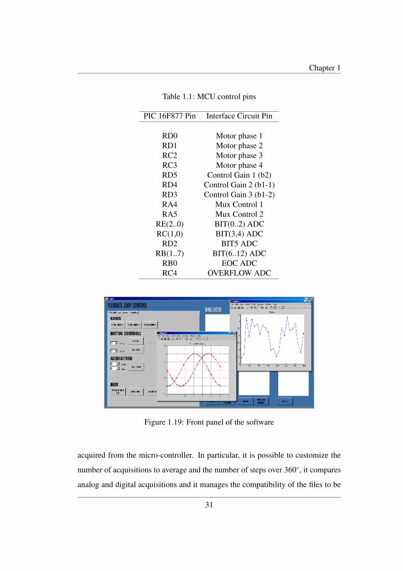
Table 1.1: MCU control pins
PIC 16F877 Pin Interface Circuit Pin
RD0 Motor phase 1RD1 Motor phase 2RC2 Motor phase 3RC3 Motor phase 4RD5 Control Gain 1 (b2)RD4 Control Gain 2 (b1-1)RD3 Control Gain 3 (b1-2)RA4 Mux Control 1RA5 Mux Control 2
RE(2..0) BIT(0..2) ADCRC(1,0) BIT(3,4) ADC
RD2 BIT5 ADCRB(1..7) BIT(6..12) ADC
RB0 EOC ADCRC4 OVERFLOW ADC
Figure 1.19: Front panel of the software
acquired from the micro-controller. In particular, it is possible to customize the
number of acquisitions to average and the number of steps over 360, it compares
analog and digital acquisitions and it manages the compatibility of the files to be
31

Chapter 1
processed with Matlab. Furthermore it can verify the measurement setup with
dedicated system check software routines.
1.3.4 Acquisition system optimization
The proposed fully automated acquisition setup is the result of an optimization
process, which started from a manual approach. In the very first acquisition setup,
the sensor was mounted on a plastic disc, which was manually rotated upon a table
with 5reference marks. The output signal of the sensing coils was subtracted
by means of a simple operational amplifier based circuit (because of coupling
effects it was not possible to simply connect the sensing coils in anti-series). The
difference was further amplified with a gain of 100 and read-out with a spectrum
analyzer. In spite of the intrinsic sensitivity of the spectrum analyzer this approach
lead to a maximum angular error of about 4.5. Partially this was caused by the
manual rotation of the system and partially by the fact that, because of the time
required by the spectrum analyzer to make a measurement, a single acquisition
per position was performed. A first improvement was the introduction of the
integrated read-out circuit, which provides a dc voltage directly proportional to
the measured field: this signal is available continuously and it is easier to perform
an average over a number of subsequent measurements. At this stage the internal
average of a Keithley 2000 multimeter was used.
Finally, the proposed acquisition system was introduced, providing a number of
benefits:
• the system has a high degree of integration, even in the auxiliary circuitry,
helping in improving the signal-to-noise ratio;
• the chance of making errors while reading the data is strongly reduced;
• the precision of the mechanical rotation is as high as 0.1;
32

Chapter 1
• speed is maximized.
This last characteristic is relevant, since it allows to increase the number of av-
eraged acquisitions for a given position and for a given total time required for a
full rotation. Alternatively, the time required for the 360rotation can be mini-
mized for a given number of averages, lowering the probability of local magnetic
perturbation during the measurement (it is worth stressing the fact that the used
approach measures the actual Earth magnetic field). In general this automatic
acquisition system allows measurements to be performed with up to 720 steps,
leading to a much finer angle discretization than the 5used for the manual ro-
tation. The angular accuracy in the reconstructed position is then improved, as
shown in Fig. 1.20. All the values of angular accuracy reported in Fig. 1.20 are
calculated by applying fixed calibration coefficients for correcting offset and gain
differences between the two axes (for each setup the coefficients are determined
from one measurement and the used for any further measurements).
5
4
3
2
1
0
Ang
ular
Acc
urac
y [D
egre
e]
ManualPositioning
BenchInstrumentation
ManualPositioning
Integrated CircuitRead-Out
Manual PositioningSemi-Automated
Acquisition(with Averages)
Fully-AutomatedPositioning
andRead-Out
Figure 1.20: Angular accuracy as a function of the acquisition system evolution
33
Chapter 1
1.3.5 Experimental results
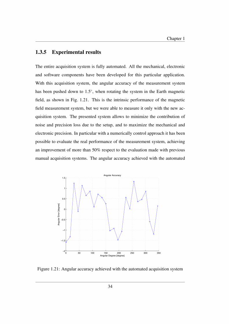
The entire acquisition system is fully automated. All the mechanical, electronic
and software components have been developed for this particular application.
With this acquisition system, the angular accuracy of the measurement system
has been pushed down to 1.5, when rotating the system in the Earth magnetic
field, as shown in Fig. 1.21. This is the intrinsic performance of the magnetic
field measurement system, but we were able to measure it only with the new ac-
quisition system. The presented system allows to minimize the contribution of
noise and precision loss due to the setup, and to maximize the mechanical and
electronic precision. In particular with a numerically control approach it has been
possible to evaluate the real performance of the measurement system, achieving
an improvement of more than 50% respect to the evaluation made with previous
manual acquisition systems. The angular accuracy achieved with the automated
0 50 100 150 200 250 300 350−2
−1.5
−1
−0.5
0
0.5
1
1.5Angular Accuracy
Ang
ular
Err
or [d
egre
e]
Angular Degree [degree]
Figure 1.21: Angular accuracy achieved with the automated acquisition system
34
Chapter 1
acquisition system is limited only by the fluxgate sensor and the read-out circuit,
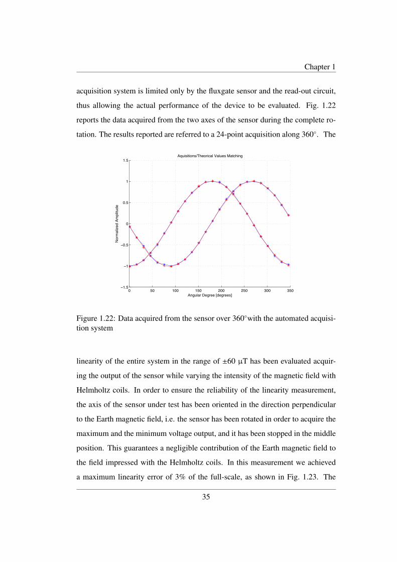
thus allowing the actual performance of the device to be evaluated. Fig. 1.22
reports the data acquired from the two axes of the sensor during the complete ro-
tation. The results reported are referred to a 24-point acquisition along 360. The
0 50 100 150 200 250 300 350−1.5
−1
−0.5
0
0.5
1
1.5Aquisitions/Theorical Values Matching
Angular Degree [degrees]
Nor
mal
ized
Am
plitu
de
Figure 1.22: Data acquired from the sensor over 360with the automated acquisi-tion system
linearity of the entire system in the range of ±60 µT has been evaluated acquir-
ing the output of the sensor while varying the intensity of the magnetic field with
Helmholtz coils. In order to ensure the reliability of the linearity measurement,
the axis of the sensor under test has been oriented in the direction perpendicular
to the Earth magnetic field, i.e. the sensor has been rotated in order to acquire the
maximum and the minimum voltage output, and it has been stopped in the middle
position. This guarantees a negligible contribution of the Earth magnetic field to
the field impressed with the Helmholtz coils. In this measurement we achieved
a maximum linearity error of 3% of the full-scale, as shown in Fig. 1.23. The
35

Chapter 1
800
600
400
200
0
-800
-600
-400
-200
-1000
LSB
-80 -60 -40 -20 0 20 40 60 80
Magnetic Induction [µT]
Figure 1.23: Linearity of the complete system
sensitivity obtained is 11 LSB/µT that corresponds to 0.45 mV/µT, considering a
300-mV ADC input voltage swing. All the data collected are in agreement with
the performance of the sensor stand-alone, previously measured with dedicated
test equipment [12].
1.4 Re-Design of the Fluxgate Magnetic Sensor In-terface Circuit
In this section a re-design of the Fluxgate magnetic sensor interface circuit is
presented. The new interface circuits targets current measurement applications
instead of electronic compasses. The re-design was aimed to reduce the supply
voltage and the power consumption of the available interface circuit, thus achiev-
ing a complete low-voltage, low-power and high linearity device. The integrated
circuit provides the correct excitation signal to the Fluxgate sensors and reads-out
the sensor signals from the sensing coils. The designed circuit allows us to deal
36
Chapter 1
with sensors featuring different values of the excitation coil resistance and to pro-
cess the sensing coil signals with a power consumption lower than 1 mW. The
interface circuit consists of three different modules, namely a timing block, an ex-
citation block and a read-out chain. The interface circuit, has been implemented
with two different excitation circuits, operating at 5 V and 3.3 V, respectively,
without any high-voltage process options. The read-out chain performs a syn-
chronous demodulation of the even harmonics, in order to extract the value of the
external magnetic field. Furthermore, it is possible to switch-on a 13 bit ADC, to
provide at the output the demodulated signal as a digital word.
1.4.1 Introduction
When Fluxgate magnetic sensors are used for current measurements, the elec-
tronic interface circuit plays an important role, since it must guarantee high linear-
ity, low-power consumption (for portable applications), reliable results and high
magnetic noise rejection. The designed circuit allows us to excite sensors with
different values of the excitation coil resistance and to process the sensor signals.
The chip consists of three different modules, namely a timing block, an excitation
block and a read-out chain. The interface circuit, whose block diagram is shown in
Fig. 1.24, has been implemented with two different excitation circuits, operating
at 5 V and 3.3 V, respectively, without any high-voltage stage [17]. The read-out
circuit allows us to retrieve the information on the external magnetic field from the
sensing coil signal. In the interface circuit, we included also a 13 bit ADC [13],
to provide the measured magnetic field value as a digital word. The timing block
provides control signals for both excitation and sensing. In the considered current
measurement application, we have used a fluxgate sensor with an excitation coil
featuring 140 Ω resistance and 4 µH inductance, which needs to be excited with a
23 mA current signal with odd symmetry at 100 kHz [10].
37
Chapter 1
Biasing Timing
Excitation5 V
Excitation3.3 V
Readout Chain ADC
+
+
+
Figure 1.24: System block diagram
1.4.2 Excitation circuits
As already mentioned, we implemented two different excitation circuits, namely
a 3.3 V supplied circuit and a 5 V supplied circuit. The first circuit requires the
use of an external inductance, while the second is fully integrated. Both circuits
provide a 36 mA triangular excitation current at 100 kHz.
3.3-V excitation circuit
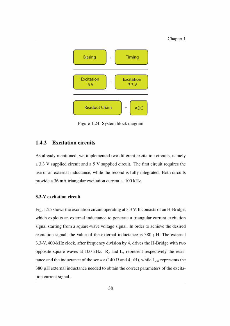
Fig. 1.25 shows the excitation circuit operating at 3.3 V. It consists of an H-Bridge,
which exploits an external inductance to generate a triangular current excitation
signal starting from a square-wave voltage signal. In order to achieve the desired
excitation signal, the value of the external inductance is 380 µH. The external
3.3-V, 400-kHz clock, after frequency division by 4, drives the H-Bridge with two
opposite square waves at 100 kHz. Rs and Ls represent respectively the resis-
tance and the inductance of the sensor (140 Ω and 4 µH), while Lext represents the
380 µH external inductance needed to obtain the correct parameters of the excita-
tion current signal.
38
Chapter 1
Rs Ls Lext
Vdd
gnd
2S1S
T Q
Q
CLK
T Q
Q
CLK
Vdd Vdd
CLK
S1
S2
M1 M2
M3 M4
Figure 1.25: Schematic of the 3.3 V excitation circuit
Signals S1 and S2 switch at 100 kHz. The aspect ratio of all transistors is 10 mm/0.4 µm.
Fig. 1.26 shows the excitation current waveform obtained in simulation.
20m
10m
0.0
-10m
-20m
-30m
( A )
0.0 30u 60u 90utime ( s )
Figure 1.26: Excitation current waveform obtained in simulation with the 3.3-Vexcitation circuit
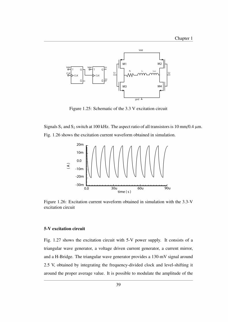
5-V excitation circuit
Fig. 1.27 shows the excitation circuit with 5-V power supply. It consists of a
triangular wave generator, a voltage driven current generator, a current mirror,
and a H-Bridge. The triangular wave generator provides a 130-mV signal around
2.5 V, obtained by integrating the frequency-divided clock and level-shifting it
around the proper average value. It is possible to modulate the amplitude of the
39
Chapter 1
+
-
+
-
+
-
Rs Ls
gnd
2S1SVref2
Vref
+
-
Vref2
Vdd2 Vdd
2
Vdd2
Vdd
S1
S1
S2
T Q
Q
CLK
S1
S2
Vdd
Clk
R1
R2
R3
R4
C1
R5
R6R7
Rrif
M1
M2
4M3M
M5
M6 M7
M8 M9
Figure 1.27: Schematic of the 5-V excitation circuit
signal changing the value of Vref. The Wilson current mirror amplifies the current
by K = 10, thus leading to a 20-mA peak current signal. The 200-kHz H-Bridge
driving signals are used to switch alternatively the direction of the current flowing
into the excitation coil of the sensor. In particular, when signal S 1 is high and
signal S 2 is low, transistors M3 and M7 are switched-on, while transistors M6 and
M5 are switched-off. During this period, the current flowing through the sensor
is KIref. By contrast, when signal S 1 is low and signal S 2 is high, transistors M6
and M5 are switched-on, and the excitation current flowing through the sensor is
−KIref. As a result, the sensor is excited with a 40-mA peak-to-peak current, as
required. Without the H-Bridge, this behavior would have been possible only with
a symmetric supply voltage (±5 V).
Triangular waveform generator
Fig. 1.28 shows the schematic of the circuit used to generate the triangular wave-
form of the excitation signal at a frequency of 100 kHz. Table 1.2 summarizes the
parameters of the devices used in the circuit of Fig. 1.28. The main clock signal
is at 400 kHz, and it is provided from outside the chip. A flip-flop is used as fre-
quency divider, providing signals S1 and S2 at 200 kHz. When S1 is high and S2 is
40
Chapter 1
+
-
+
-
Vref2
Vref
+
-
Vref2
Vdd2 Vdd
2
S1
S1
S2
T Q
Q
CLK
S1
S2
Vdd
Clk
R1
R2
R3
R4
C1
R5
R6R7
A1A2
A3
V1V2 Vout
Figure 1.28: Triangular waveform generator
Table 1.2: Design parameters of the triangular waveform generator
R1 R2 R3 R4 R5 R6 R7 C1
37 kΩ 37 kΩ 1.25 MΩ 1 MΩ 37 kΩ 37 kΩ 37 kΩ 1pF
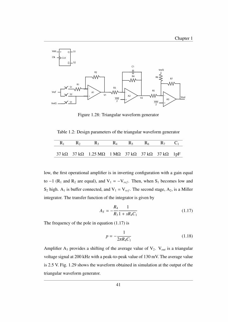
low, the first operational amplifier is in inverting configuration with a gain equal
to −1 (R1 and R2 are equal), and V1 = −Vre f . Then, when S1 becomes low and
S2 high. A1 is buffer connected, and V1 = Vre f . The second stage, A2, is a Miller
integrator. The transfer function of the integrator is given by
AS = −R4
R3
11 + sR4C1
(1.17)
The frequency of the pole in equation (1.17) is
p = −1
2πR4C1(1.18)
Amplifier A3 provides a shifting of the average value of V2. Vout is a triangular
voltage signal at 200 kHz with a peak-to-peak value of 130 mV. The average value
is 2.5 V. Fig. 1.29 shows the waveform obtained in simulation at the output of the
triangular waveform generator.
41
Chapter 1
2.670
2.610
2.550
2.490
( V )
150u 190u 230u 270utime ( s )
Figure 1.29: Waveform obtained in simulation at the output of the triangular wave-form generator
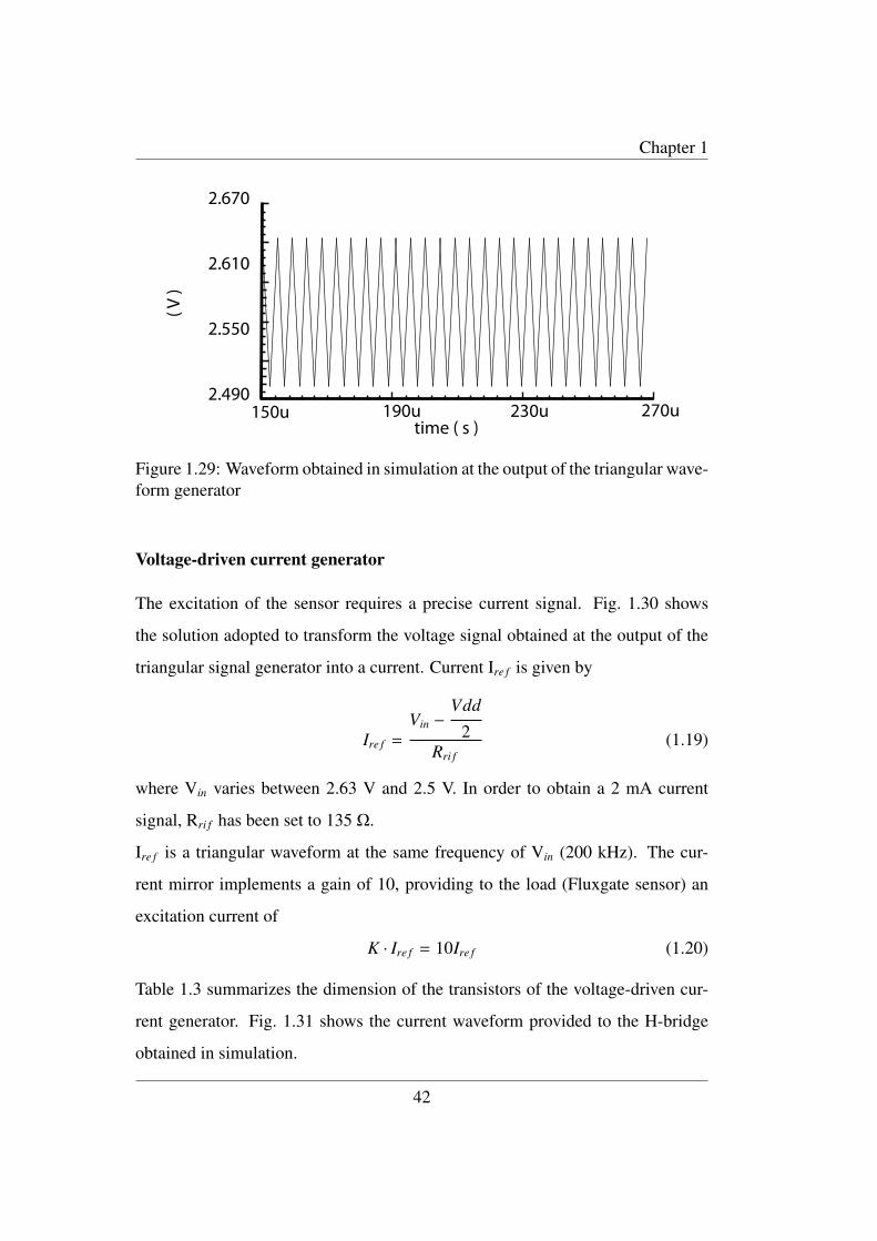
Voltage-driven current generator
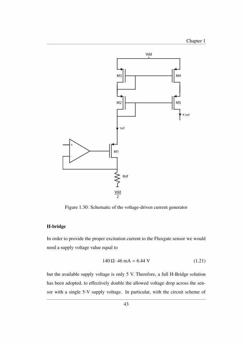
The excitation of the sensor requires a precise current signal. Fig. 1.30 shows
the solution adopted to transform the voltage signal obtained at the output of the
triangular signal generator into a current. Current Ire f is given by
Ire f =
Vin −Vdd
2Rri f
(1.19)
where Vin varies between 2.63 V and 2.5 V. In order to obtain a 2 mA current
signal, Rri f has been set to 135 Ω.
Ire f is a triangular waveform at the same frequency of Vin (200 kHz). The cur-
rent mirror implements a gain of 10, providing to the load (Fluxgate sensor) an
excitation current of
K · Ire f = 10Ire f (1.20)
Table 1.3 summarizes the dimension of the transistors of the voltage-driven cur-
rent generator. Fig. 1.31 shows the current waveform provided to the H-bridge
obtained in simulation.
42
Chapter 1
+
-
Vdd2
Vdd
Rrif
M1
M2
M3 M4
M5
K Iref
Iref
Figure 1.30: Schematic of the voltage-driven current generator
H-bridge
In order to provide the proper excitation current to the Fluxgate sensor we would
need a supply voltage value equal to
140 Ω · 46 mA = 6.44 V (1.21)
but the available supply voltage is only 5 V. Therefore, a full H-Bridge solution
has been adopted, to effectively double the allowed voltage drop across the sen-
sor with a single 5-V supply voltage. In particular, with the circuit scheme of
43
Chapter 1
Table 1.3: Design parameters of the of the voltage-driven current generator
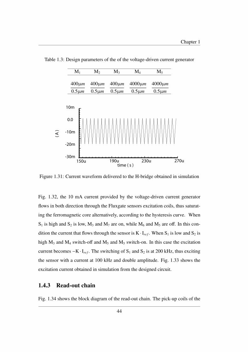
M1 M2 M3 M4 M5
400µm
0.5µm
400µm
0.5µm
400µm
0.5µm
4000µm
0.5µm
4000µm
0.5µm
10m
-10m
-20m
-30m
( A )
150u 190u 230u 270utime ( s )
0.0
Figure 1.31: Current waveform delivered to the H-bridge obtained in simulation
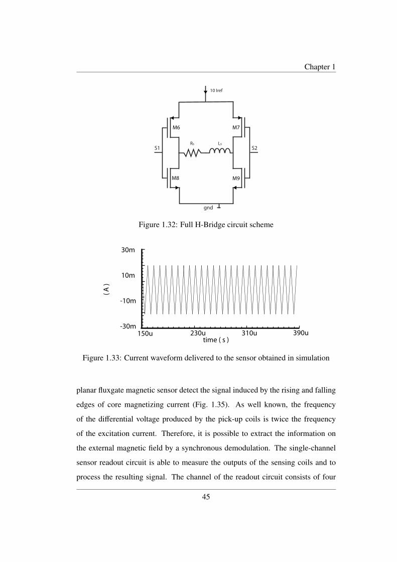
Fig. 1.32, the 10 mA current provided by the voltage-driven current generator
flows in both direction through the Fluxgate sensors excitation coils, thus saturat-
ing the ferromagnetic core alternatively, according to the hysteresis curve. When
S1 is high and S2 is low, M3 and M7 are on, while M6 and M5 are off. In this con-
dition the current that flows through the sensor is K · Ire f . When S1 is low and S2 is
high M3 and M4 switch-off and M5 and M5 switch-on. In this case the excitation
current becomes −K · Ire f . The switching of S1 and S2 is at 200 kHz, thus exciting
the sensor with a current at 100 kHz and double amplitude. Fig. 1.33 shows the
excitation current obtained in simulation from the designed circuit.
1.4.3 Read-out chain
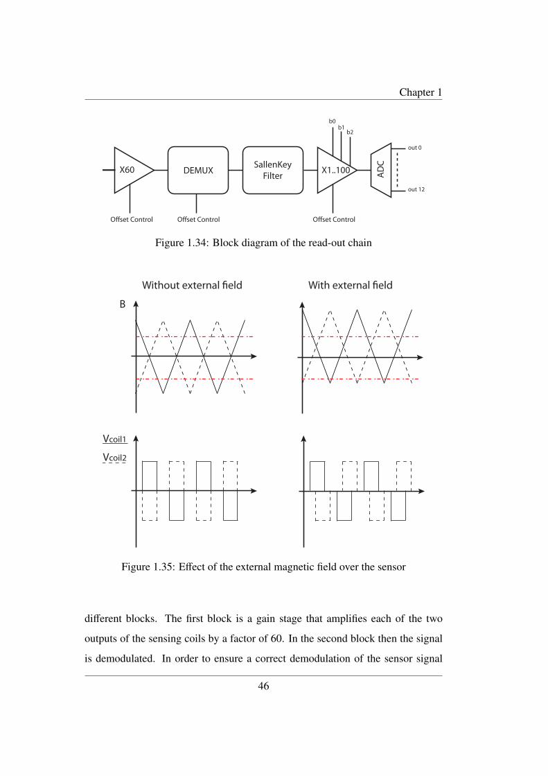
Fig. 1.34 shows the block diagram of the read-out chain. The pick-up coils of the
44
Chapter 1
Rs Ls
gnd
S1 S2
M6 M7
M8 M9
10 Iref
Figure 1.32: Full H-Bridge circuit scheme
30m
-10m
-30m
( A )
150u 230u 310u 390utime ( s )
10m
Figure 1.33: Current waveform delivered to the sensor obtained in simulation
planar fluxgate magnetic sensor detect the signal induced by the rising and falling
edges of core magnetizing current (Fig. 1.35). As well known, the frequency
of the differential voltage produced by the pick-up coils is twice the frequency
of the excitation current. Therefore, it is possible to extract the information on
the external magnetic field by a synchronous demodulation. The single-channel
sensor readout circuit is able to measure the outputs of the sensing coils and to
process the resulting signal. The channel of the readout circuit consists of four
45
Chapter 1
X60 X1..100 AD
C
DEMUXSallenKey
Filter
Offset Control Offset Control Offset Control
b0b1
b2
out 0
out 12
Figure 1.34: Block diagram of the read-out chain
Without external field With external field
B
Vcoil1
Vcoil2
Figure 1.35: Effect of the external magnetic field over the sensor
different blocks. The first block is a gain stage that amplifies each of the two
outputs of the sensing coils by a factor of 60. In the second block then the signal
is demodulated. In order to ensure a correct demodulation of the sensor signal
46

Chapter 1
and to avoid problems due to the asynchronicity between the clock and the output
of the sensor itself, a quadrature demodulation has been implemented. Using this
technique and adding together the contribution of the two orthogonal signals, it is
possible to avoid errors due to timing misalignments between the readout clock
and the output of the sensor. The readout process is done at a frequency equal to
200 kHz. The third block is a second order Sallen-Key low-pass filter that removes
all the high frequency components resulting from the demodulation and returns a
DC value that is proportional to the magnetic field. The difference between this
output voltage and the analog ground is then amplified with programmable gain
(from 0 to 100) in the last block.
In order to achieve low power consumption, we adopted the following solutions:
• single read-out circuit;
• dedicated operational amplifiers with low power consumption.
Therefore, we designed the following blocks:
• low charge injection switches;
• low output resistance operational amplifier with a bandwidth of 200 kHz,
with low power consumption;
• low output resistance operational amplifier with a bandwidth of 10 kHz,
with low power consumption;
• coherent quadrature demodulator;
• Sallen-Key filter with a bandwidth of 500 Hz;
• variable gain operational amplifier.
47
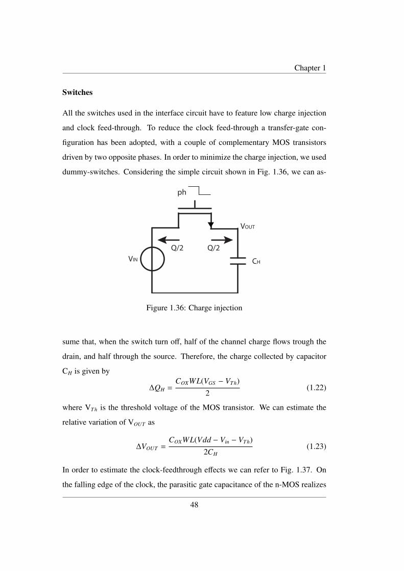
Chapter 1
Switches
All the switches used in the interface circuit have to feature low charge injection
and clock feed-through. To reduce the clock feed-through a transfer-gate con-
figuration has been adopted, with a couple of complementary MOS transistors
driven by two opposite phases. In order to minimize the charge injection, we used
dummy-switches. Considering the simple circuit shown in Fig. 1.36, we can as-
ph
Q/2 Q/2
CH
VOUT
VIN
Figure 1.36: Charge injection
sume that, when the switch turn off, half of the channel charge flows trough the
drain, and half through the source. Therefore, the charge collected by capacitor
CH is given by
∆QH =COXWL(VGS − VTh)
2(1.22)
where VTh is the threshold voltage of the MOS transistor. We can estimate the
relative variation of VOUT as
∆VOUT =COXWL(Vdd − Vin − VTh)
2CH(1.23)
In order to estimate the clock-feedthrough effects we can refer to Fig. 1.37. On
the falling edge of the clock, the parasitic gate capacitance of the n-MOS realizes
48
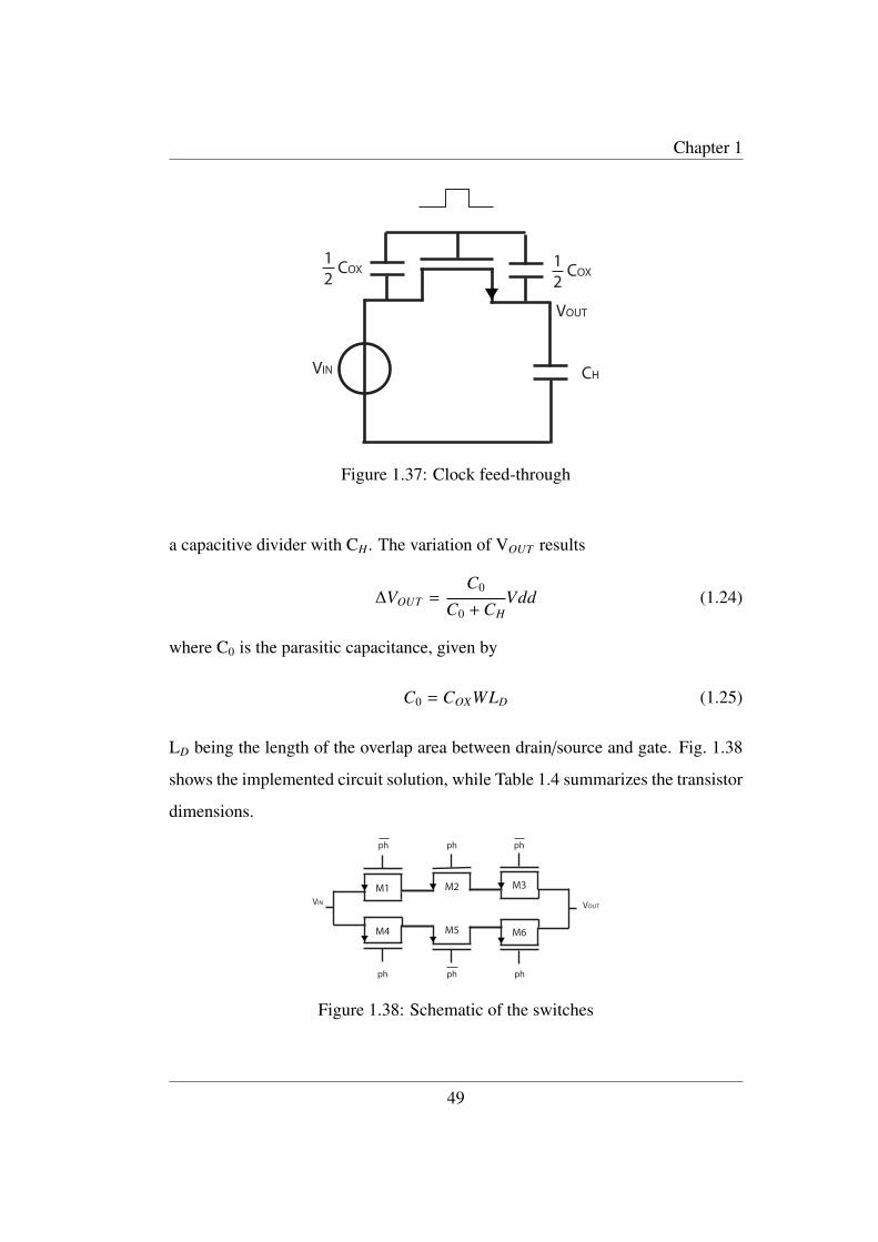
Chapter 1
CH
VOUT
VIN
12COX 1
2COX
Figure 1.37: Clock feed-through
a capacitive divider with CH. The variation of VOUT results
∆VOUT =C0
C0 + CHVdd (1.24)
where C0 is the parasitic capacitance, given by
C0 = COXWLD (1.25)
LD being the length of the overlap area between drain/source and gate. Fig. 1.38
shows the implemented circuit solution, while Table 1.4 summarizes the transistor
dimensions.
VIN VOUT
ph ph ph
ph phph
M1 M2 M3
M4 M5 M6
Figure 1.38: Schematic of the switches
49
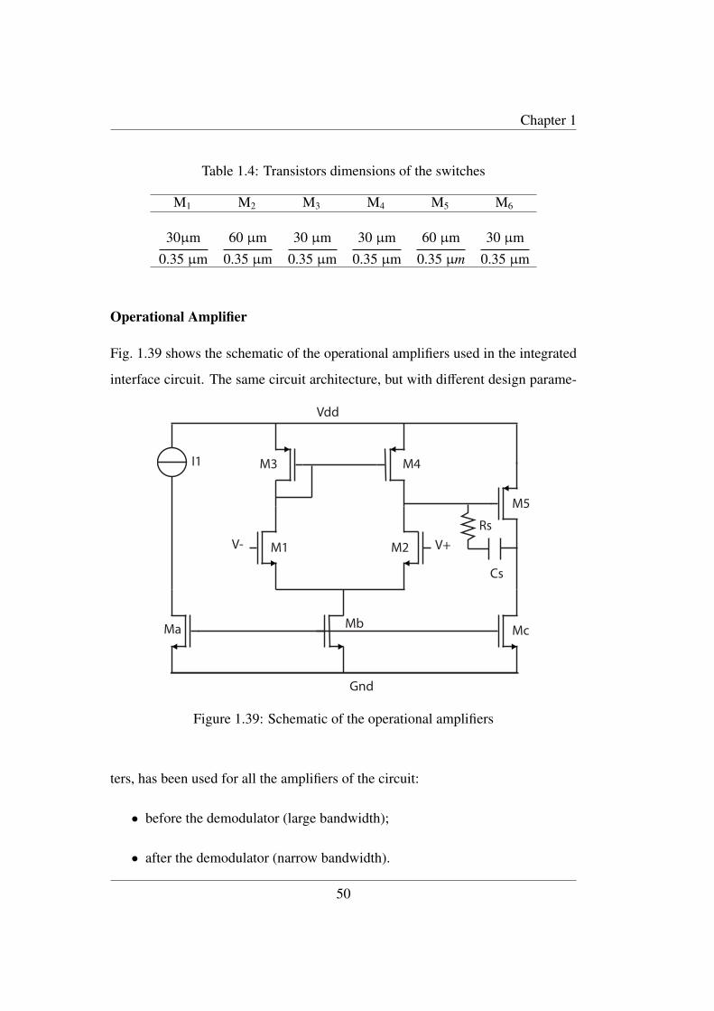
Chapter 1
Table 1.4: Transistors dimensions of the switches
M1 M2 M3 M4 M5 M6
30µm0.35 µm
60 µm0.35 µm
30 µm0.35 µm
30 µm0.35 µm
60 µm0.35 µm
30 µm0.35 µm
Operational Amplifier
Fig. 1.39 shows the schematic of the operational amplifiers used in the integrated
interface circuit. The same circuit architecture, but with different design parame-
V- V+Rs
Cs
M3 M4
M1 M2
M5
MbMa Mc
I1
Vdd
Gnd
Figure 1.39: Schematic of the operational amplifiers
ters, has been used for all the amplifiers of the circuit:
• before the demodulator (large bandwidth);
• after the demodulator (narrow bandwidth).
50

Chapter 1
The amplifiers used before and after the demodulator are different in terms of
transistor dimensions and bis current, thus featuring different power consumption,
bandwidth and gain.
The structure of Fig. 1.39 consists of two stages. The low-frequency gain is given
by
Av = A1A2 =gm1gm5
(gm2 + gm4)(gm5 + gmc)(1.26)
To study the operational amplifier behavior at high frequency, we can refer to the
equivalent circuit shown in Fig. 1.40. Resistor R1 represents the output resistance
gm1 Vin
R1
Cc Rc
C1
gm5 V1
V1
R2 C2
V0
Figure 1.40: Equivalent circuit of the operational amplifier
of the first stage (R1 = r02//r04), while R2 is the output resistance of the second
stage (R2 = r05//r0C), C1 is the total capacitance between the first and the second
stage, and C2 the output capacitance.
The transfer function of the circuit is
Vo
Vin= Av
[1 + s(Rc − 1/gm5)Cc](1 +
s
p1
)(1 +
s
p2
) (1.27)
where
p1 '− 1
gm5R2R1CC(1.28)
and
p2 '− gm5CC
C1C2 + (C1 + C2)CC(1.29)
51

Chapter 1
This transfer function features also a zero placed at
z =1
(RC − 1/gm5)CC(1.30)
If we assume that the pole given by equation (1.28) is the dominant pole, we
obtain a gain-bandwidth product given by
fT =gm1
2πCC(1.31)
In order to obtain the best transistor dimensions for achieving the desired specifi-
cations, we used the gm/ID method. The curve gm/ID reduces the range of values
for the best dimension search. The relation between gm/ID and the bias point of
the transistors can be explained using the definition of gm, that is
gm
ID=
1ID
δID
δVGS
∣∣∣∣∣∣VDS =constant
=δlog(ID)δVGS
∣∣∣∣∣∣VDS =constant
(1.32)
This relation can be obtained in two ways:
• experimentally;
• analytically (or by means of circuital simulators).
We adopted the second method, even if the results are closely dependent on the
reliability of the used transistor models (Fig. 1.41).
The cutoff frequency of the operational amplifiers before the demodulator must
be higher than 200 kHz, for obvious reasons. The resulting dimensioning of this
family of operational amplifiers is summarized in Table 1.5. Fig. 1.42 shows the
Bode diagram of the operational amplifiers dimensioned according to Table 1.5.
The operational amplifiers used after the demodulator require low bandwidth and
slew-rate, because the information contents of the Fluxgate sensing coils signal
has already been down-converted to dc. Therefore, the focus has been put on
minimizing the power consumption. The dimensions of the transistors used are
52
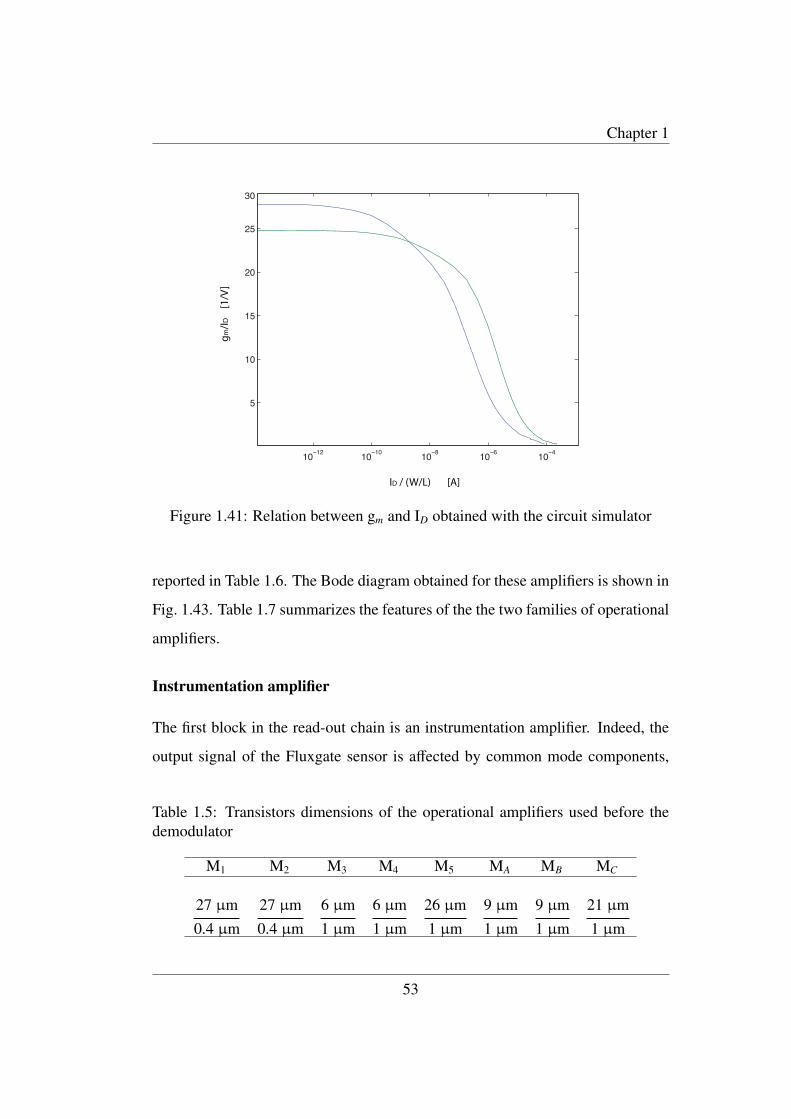
Chapter 1
10−12
10−10
10−8
10−6
10−4
5
10
15
20
25
30
gm/ID
[1
/V]
ID / (W/L) [A]
Figure 1.41: Relation between gm and ID obtained with the circuit simulator
reported in Table 1.6. The Bode diagram obtained for these amplifiers is shown in
Fig. 1.43. Table 1.7 summarizes the features of the the two families of operational
amplifiers.
Instrumentation amplifier
The first block in the read-out chain is an instrumentation amplifier. Indeed, the
output signal of the Fluxgate sensor is affected by common mode components,
Table 1.5: Transistors dimensions of the operational amplifiers used before thedemodulator
M1 M2 M3 M4 M5 MA MB MC
27 µm0.4 µm
27 µm0.4 µm
6 µm1 µm
6 µm1 µm
26 µm1 µm
9 µm1 µm
9 µm1 µm
21 µm1 µm
53
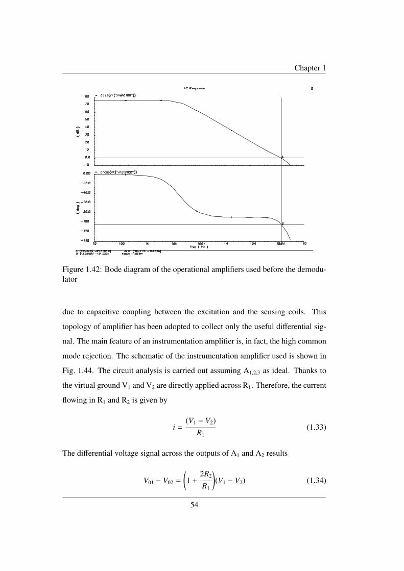
Chapter 1
Figure 1.42: Bode diagram of the operational amplifiers used before the demodu-lator
due to capacitive coupling between the excitation and the sensing coils. This
topology of amplifier has been adopted to collect only the useful differential sig-
nal. The main feature of an instrumentation amplifier is, in fact, the high common
mode rejection. The schematic of the instrumentation amplifier used is shown in
Fig. 1.44. The circuit analysis is carried out assuming A1,2,3 as ideal. Thanks to
the virtual ground V1 and V2 are directly applied across R1. Therefore, the current
flowing in R1 and R2 is given by
i =(V1 − V2)
R1(1.33)
The differential voltage signal across the outputs of A1 and A2 results
V01 − V02 =
(1 +
2R2
R1
)(V1 − V2) (1.34)
54
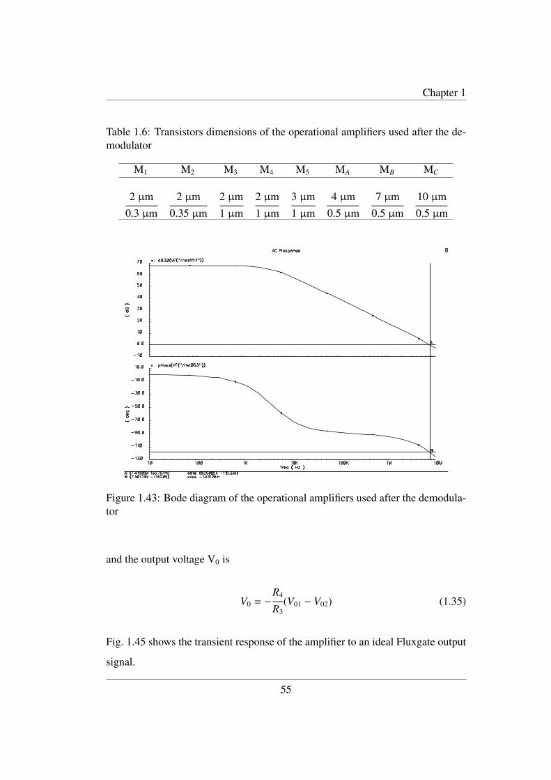
Chapter 1
Table 1.6: Transistors dimensions of the operational amplifiers used after the de-modulator
M1 M2 M3 M4 M5 MA MB MC
2 µm0.3 µm
2 µm0.35 µm
2 µm1 µm
2 µm1 µm
3 µm1 µm
4 µm0.5 µm
7 µm0.5 µm
10 µm0.5 µm
Figure 1.43: Bode diagram of the operational amplifiers used after the demodula-tor
and the output voltage V0 is
V0 = −R4
R3(V01 − V02) (1.35)
Fig. 1.45 shows the transient response of the amplifier to an ideal Fluxgate output
signal.
55
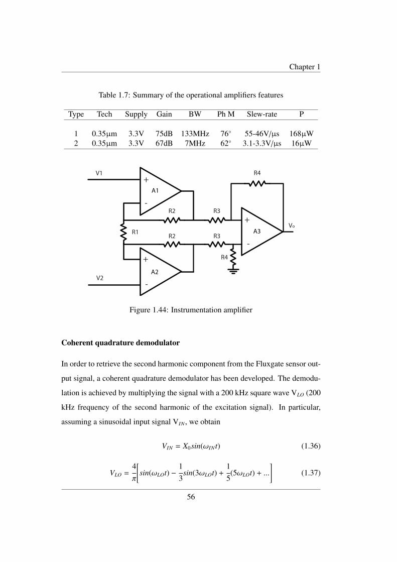
Chapter 1
Table 1.7: Summary of the operational amplifiers features
Type Tech Supply Gain BW Ph M Slew-rate P
1 0.35µm 3.3V 75dB 133MHz 76 55-46V/µs 168µW2 0.35µm 3.3V 67dB 7MHz 62 3.1-3.3V/µs 16µW
R1
R2
R2
R3
R3
V1
V2
Vo
+
+
+
-
-
-
R4
R4
A1
A2
A3
Figure 1.44: Instrumentation amplifier
Coherent quadrature demodulator
In order to retrieve the second harmonic component from the Fluxgate sensor out-
put signal, a coherent quadrature demodulator has been developed. The demodu-
lation is achieved by multiplying the signal with a 200 kHz square wave VLO (200
kHz frequency of the second harmonic of the excitation signal). In particular,
assuming a sinusoidal input signal VIN , we obtain
VIN = X0sin(ωINt) (1.36)
VLO =4π
[sin(ωLOt) −
13
sin(3ωLOt) +15(5ωLOt) + ...
](1.37)
56
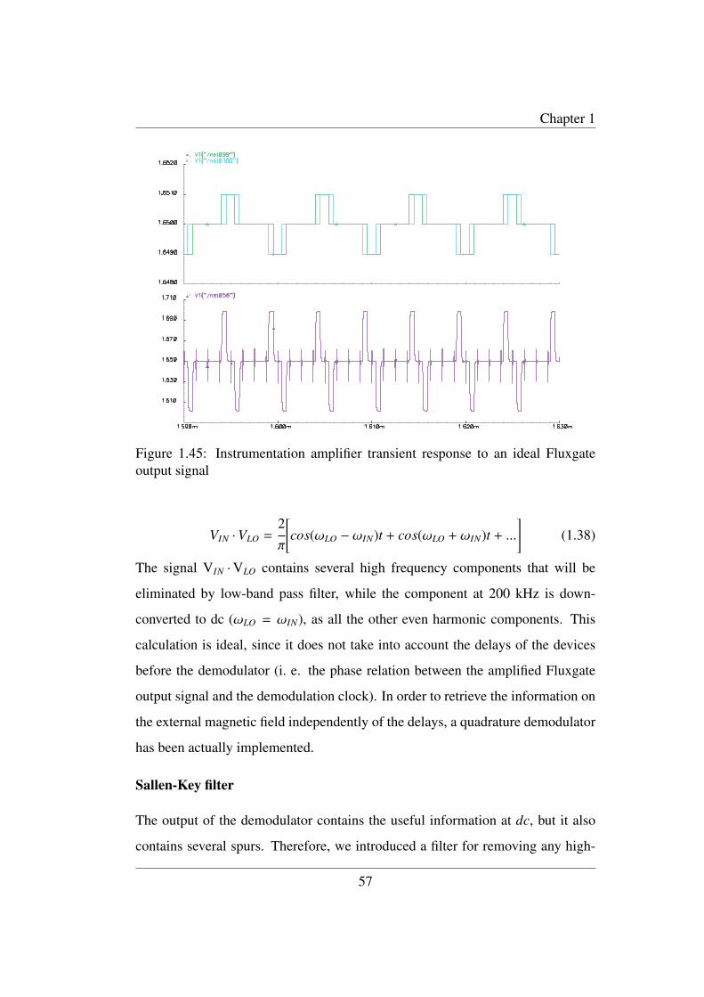
Chapter 1
Figure 1.45: Instrumentation amplifier transient response to an ideal Fluxgateoutput signal
VIN ·VLO =2π
[cos(ωLO − ωIN)t + cos(ωLO + ωIN)t + ...
](1.38)
The signal VIN ·VLO contains several high frequency components that will be
eliminated by low-band pass filter, while the component at 200 kHz is down-
converted to dc (ωLO = ωIN), as all the other even harmonic components. This
calculation is ideal, since it does not take into account the delays of the devices
before the demodulator (i. e. the phase relation between the amplified Fluxgate
output signal and the demodulation clock). In order to retrieve the information on
the external magnetic field independently of the delays, a quadrature demodulator
has been actually implemented.
Sallen-Key filter
The output of the demodulator contains the useful information at dc, but it also
contains several spurs. Therefore, we introduced a filter for removing any high-
57
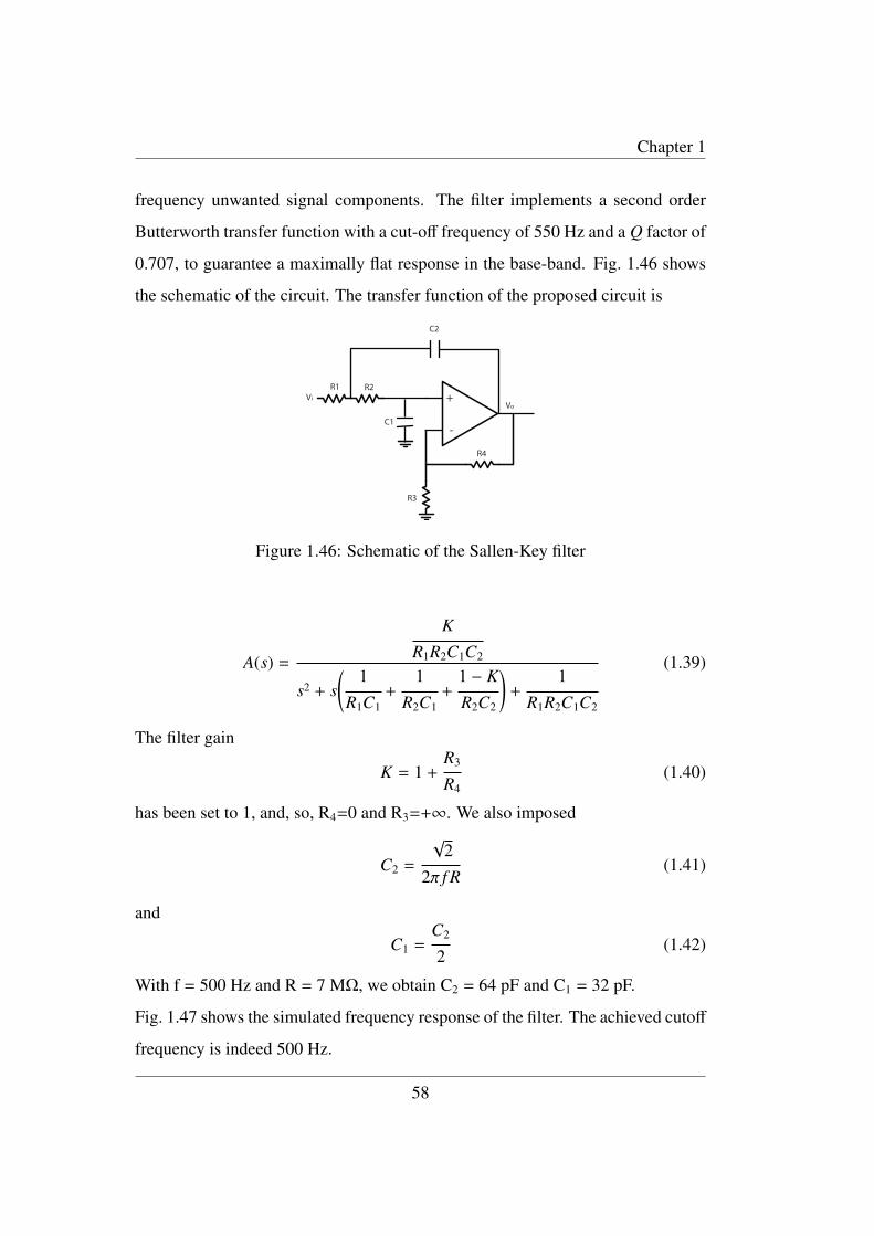
Chapter 1
frequency unwanted signal components. The filter implements a second order
Butterworth transfer function with a cut-off frequency of 550 Hz and a Q factor of
0.707, to guarantee a maximally flat response in the base-band. Fig. 1.46 shows
the schematic of the circuit. The transfer function of the proposed circuit is
R3
Vo+
-
R4
C1
C2
R1 R2Vi
Figure 1.46: Schematic of the Sallen-Key filter
A(s) =
K
R1R2C1C2
s2 + s( 1R1C1
+1
R2C1+
1 − K
R2C2
)+
1R1R2C1C2
(1.39)
The filter gain
K = 1 +R3
R4(1.40)
has been set to 1, and, so, R4=0 and R3=+∞. We also imposed
C2 =
√2
2π f R(1.41)
and
C1 =C2
2(1.42)
With f = 500 Hz and R = 7 MΩ, we obtain C2 = 64 pF and C1 = 32 pF.
Fig. 1.47 shows the simulated frequency response of the filter. The achieved cutoff
frequency is indeed 500 Hz.
58
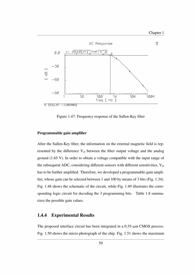
Chapter 1
Figure 1.47: Frequency response of the Sallen-Key filter
Programmable gain amplifier
After the Sallen-Key filter, the information on the external magnetic field is rep-
resented by the difference VD between the filter output voltage and the analog
ground (1.65 V). In order to obtain a voltage compatible with the input range of
the subsequent ADC, considering different sensors with different sensitivities, VD
has to be further amplified. Therefore, we developed a programmable-gain ampli-
fier, whose gain can be selected between 1 and 100 by means of 3 bits (Fig. 1.34).
Fig. 1.48 shows the schematic of the circuit, while Fig. 1.49 illustrates the corre-
sponding logic circuit for decoding the 3 programming bits. Table 1.8 summa-
rizes the possible gain values.
1.4.4 Experimental Results
The proposed interface circuit has been integrated in a 0.35-µm CMOS process.
Fig. 1.50 shows the micro-photograph of the chip. Fig. 1.51 shows the maximum
59
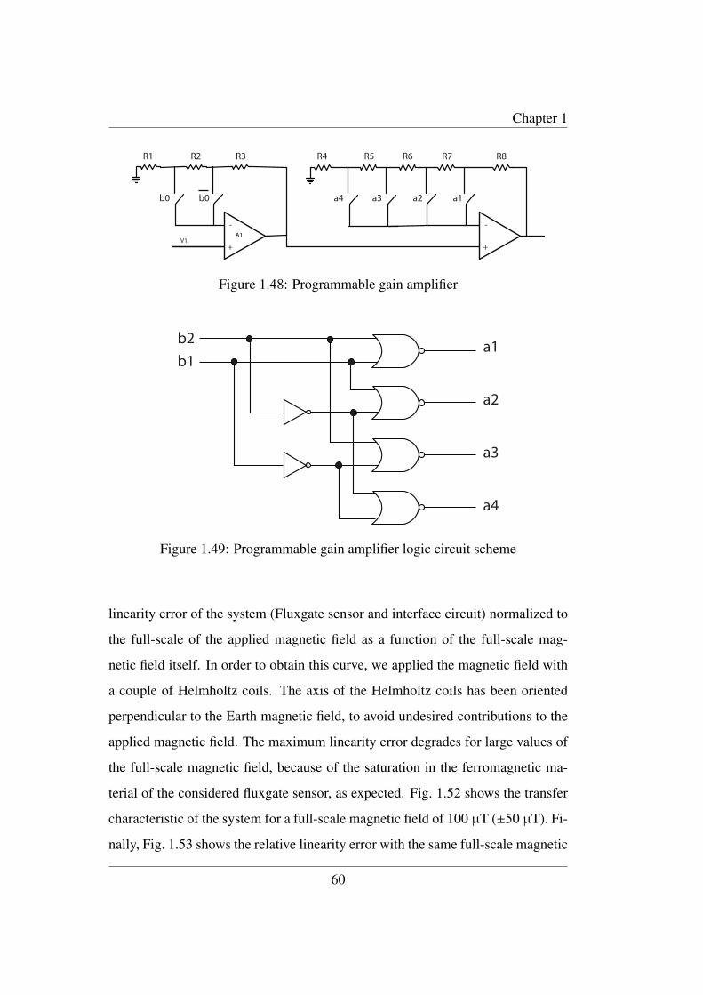
Chapter 1
V1A1
+
-
+
-
R1 R2 R3 R4 R5 R6 R7 R8
b0 b0 a4 a3 a2 a1
Figure 1.48: Programmable gain amplifier
b2b1
a1
a2
a3
a4
Figure 1.49: Programmable gain amplifier logic circuit scheme
linearity error of the system (Fluxgate sensor and interface circuit) normalized to
the full-scale of the applied magnetic field as a function of the full-scale mag-
netic field itself. In order to obtain this curve, we applied the magnetic field with
a couple of Helmholtz coils. The axis of the Helmholtz coils has been oriented
perpendicular to the Earth magnetic field, to avoid undesired contributions to the
applied magnetic field. The maximum linearity error degrades for large values of
the full-scale magnetic field, because of the saturation in the ferromagnetic ma-
terial of the considered fluxgate sensor, as expected. Fig. 1.52 shows the transfer
characteristic of the system for a full-scale magnetic field of 100 µT (±50 µT). Fi-
nally, Fig. 1.53 shows the relative linearity error with the same full-scale magnetic
60
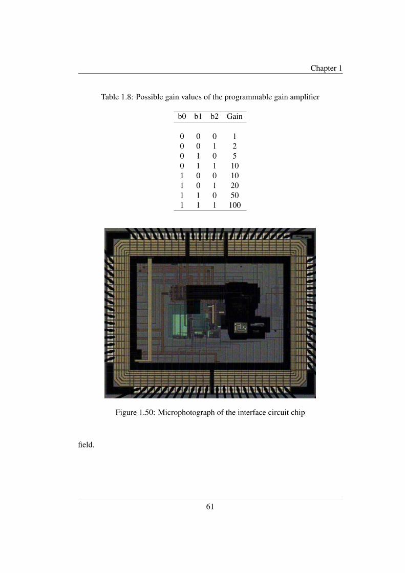
Chapter 1
Table 1.8: Possible gain values of the programmable gain amplifier
b0 b1 b2 Gain
0 0 0 10 0 1 20 1 0 50 1 1 101 0 0 101 0 1 201 1 0 501 1 1 100
Figure 1.50: Microphotograph of the interface circuit chip
field.
61
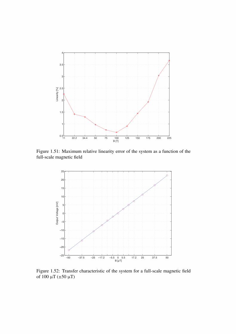
11 22.2 34.4 50 75 100 125 150 175 200 2250.5
1
1.5
2
2.5
3
3.5
4
B [T]
Line
arity
[%]
Figure 1.51: Maximum relative linearity error of the system as a function of thefull-scale magnetic field
−50 −37.5 −25 −17.2 −5.5 0 5.5 17.2 25 37.5 50−25
−20
−15
−10
−5
0
5
10
15
20
25
B [µT]
Out
put V
olta
ge [m
V]
Figure 1.52: Transfer characteristic of the system for a full-scale magnetic fieldof 100 µT (±50 µT)
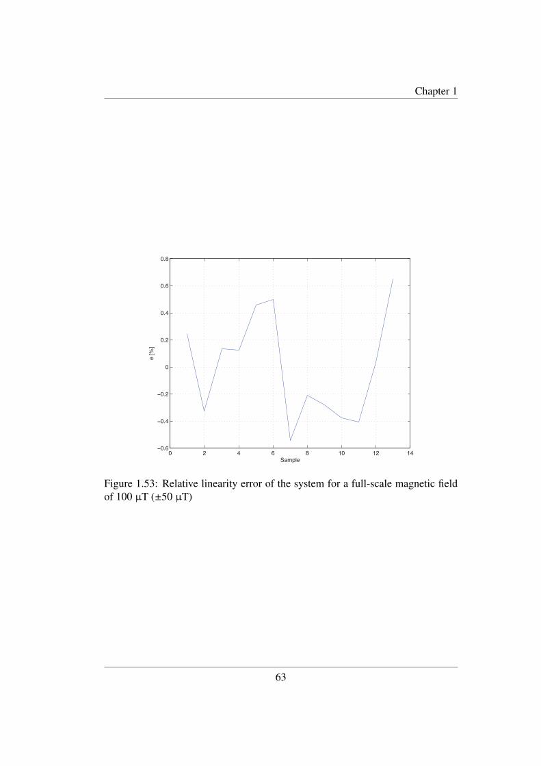
Chapter 1
0 2 4 6 8 10 12 14−0.6
−0.4
−0.2
0
0.2
0.4
0.6
0.8
e [%
]
Sample
Figure 1.53: Relative linearity error of the system for a full-scale magnetic fieldof 100 µT (±50 µT)
63

Chapter 1
64

Chapter 2
Energy Harvesting
In this chapter we present the activity on energy harvesting. Inparticular, we developed several integrated solutions to retrievethe energy needed to supply a microsystem from the environment,thus avoiding the use of batteries and making the system com-pletely autonomous. The energy source that has been consid-ered is light, and the exploited process to convert it into electricalpower is the photoelectric effect of a p-n junction on silicon, com-monly used in CMOS fabrication technology.
2.1 Introduction
Modern ultra-low-power integrated circuits have reached such a level of integra-
tion and processing efficiency that many applications no longer require traditional
batteries. These applications include complex and often power-intensive wireless
sensor networks that may involve sampling various sensors and communicating
wirelessly. By harvesting minuscule amounts of wasted energy from the envi-
ronment, such systems are enabled with near infinite up-time without a battery
as its primary power source. Not only does energy harvesting enhance current
65

Chapter 2
Pentium D 840
Pentium EE 955
Core 2 Extreme QX670
Pentium 570
Athlon 64 X2 6000+
Athlon 64 X2 FX-62
Pentium 660
Athlon 64 X2 5400+
Core 2 Extreme X6800
Core 2 Extreme E6700
Athlon 64 X2 5000+ (65nm)
Athlon 64 X2 3800+ EE
Core 2 Duo E6300 (B2)
Core 2 Duo E6300 (L2)
Sempron 3500+
Sempron 3600+
002051001050
30,96
33,26
37,36
45,49
46,45
63,39
66
66,78
86,39
93,78
106,15
119,47
123,92
126,96
137,6
140,73
5,59
5,95
8,62
12,02
6,14
7,73
15,78
20,64
8,87
22,65
9,72
11,79
29,86
24,28
54,54
42,09
Microprocesors power consumption trend
Idle state power consumption [W]Full load state power consumption [W]
Figure 2.1: Trend of power dissipation in microprocessors design field
applications by eliminating their dependency on the battery, but it also enables
entirely new applications that were not feasible given the finite lifetime and size
of batteries. Similar to Moore’s Law, which defines the trend of digital technology
to double in transistor count every two years, an inverse trend occurs for power
consumption. Roughly every 18 months, the power dissipation of digital systems
is cut in half. Despite the technology scaling, electrochemical batteries [18] are
characterized by a slow growth in terms of energy density, and represent an add
on of weight and volume, limiting the lifetime of the devices. Advancements in
power efficiency already had very significant results for small, ultra-low-power
microcontrollers (MCUs) specifically designed for battery-powered applications
and have resulted in designs where battery life has exceeded 10 years. For typ-
ical ultra-low-power MCUs, it is common for standby current to be less than 1
µA, and active current consumption in the 200 µA/MIPS range. Since the clock
rate of these MCUs is typically in the order of 25 MHz or less, the peak current
consumption is always relatively small and can be powered with simple power
supplies. Power consumption of a given application is rarely characterized by a
66

Chapter 2
single MCU’s current draw. Analog conversion circuitry, power regulation, and
communication devices each play a part in the system and consume power even
when they are not active. By integrating the functionality of each of the devices
into a single chip using a single low-power fabrication process, it is not only possi-
ble to significantly reduce the leakage current of the overall system, but by giving
a single MCU control to disable peripherals that are not in use, power consump-
tion can be reduced even further. A single, highly integrated device will typically
consume less power than separate discrete solutions; a single device also simpli-
fies the design and reduces the cost and area required for a given function.
Traditional batteries, such as lithium-ion cells, have been the default source for
power in portable electronics for decades; however, traditional batteries place hard
restrictions on product usability, lifetime, and cost of ownership. While process-
ing power roughly doubles ever two years, battery technology advances at a much
more sluggish pace. Historically, battery capacity has doubled every 10 years. In
addition to the very slow growth in their energy capacity, traditional batteries have
a limit to the total practical energy density they can provide. Present-day lithium-
ion batteries, which are popular due to their high energy-to-weight ratio, have an
energy density of 150 to 200 Wh/kg. Research has shown that it is possible to
increase their energy density by tenfold within a few years; however, even if this
is achieved, we must still consider practical safety concerns. Given improper use,
batteries with extremely high energy densities can become dangerous, explosive
devices. For most battery-operated devices, the cost associated with owning and
operating the device is rarely limited to the initial cost of manufacturing it. In
the long term, replacing the battery can have a significant impact on the overall
cost of ownership. This is especially critical in applications where battery replace-
ment is impractical or has high labor costs associated with maintenance. Take for
example water meters that must be buried underground. Accessing the water me-
67

Chapter 2
ter would require digging it up, which in colder climates might be one meter or
deeper underground. Thanks to this unavoidable inaccessibility, the replacement
cost of the battery could be in the $100 to $200 range per water meter. Miniatur-
ization of products has been an ongoing trend in most application spaces, but the
driving force has come from consumer electronics and medical applications. For
consumer products, the demand for smaller and sleeker devices has driven inno-
vation for more highly integrated electronics given the finite amount of space that
products are expect to take up. While integration at the IC level has kept up with
consumer demand, the power source is not benefiting from miniaturization. The
space allowed for batteries is shrinking, the lifetime for which they are expected
to operate is longer, and the amount of power they are expected to provide has
also increased. The requirements for batteries in modern electronics have far ex-
ceeded what can be delivered. Despite the challenges with traditional batteries, it
is possible to maintain functionality with today rechargeable batteries, or we may
even forgo the battery altogether if we couple an ultra-low-power embedded pro-
cessor with a power supply that harvests energy from its environment. Alternative
power sources could extend the lifetime of low-power systems, such as mobile
and sensor nodes[19], reducing the volume-dependency and the weight. There-
fore, harvesting systems [20] [21] [22] are becoming the new challenge in both
research and commercial communities. In most cases, in fact, the final device is
located in environments with many energy sources, such as lights, vibrations or
thermal gradients. In this case energy scavenging represents an optimum option
to increase the performance of the device.
2.2 Micro Energy Harvesting
In principle, energy harvesting has been around for thousands of years. The first
waterwheels have been dated back to as far as the fourth century B.C. The wa-
68

Chapter 2
terwheel effectively harvested the energy from flowing water and transferred it
to mechanical energy. Similarly, present-day wind farms or solar arrays all use
the same principle of operation and usually provide power back to the main grid.
These large-scale applications can be referred to as macro energy harvesting. On
the other hand, micro energy harvesting, which we will be focusing on, is the
principle that enables small, autonomous devices to capture energy from the envi-
ronment and store it. While micro and macro energy harvesting may be similar in
principle, their scope and applications are radically different. The portion of the
system that harvests energy consists of two main parts:
• the component that converts the ambient energy from the environment;
• a means of storing the energy for later use by the application.
Although the rest of the system can be defined in an infinite number of ways and is
dependent on the task at hand, energy-harvesting systems typically contain similar
components given that they are ideal for sensor network applications. An ultra-
low-power MCU will be the heart of the system and is responsible for the majority
of the processing, sensing, and communication. The MCU will interface to any
number of sensors to collect data from its environment and will usually transfer
or receive data via a wireless transceiver. Since energy harvesting systems are
completely untethered, they each act as autonomous systems. The sources of en-
ergy to harvest are similarly numerous, and more esoteric systems continue to
be introduced. However, the most common sources for ambient energy are light,
thermal, radio frequency (RF), and vibration. The characteristics of typical energy
harvesters are summarized in Table 2.1. Each has unique advantages and disad-
vantages, and the specific harvesting technology is dependent on the application
and the use case. Clearly, a device outfitted with a solar panel would not benefit if
it sits in a dark cave all day. The key to an energy-harvesting system is to take en-
69
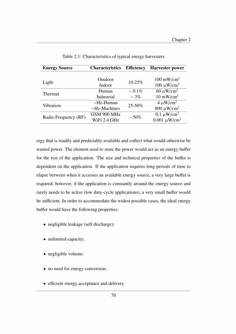
Chapter 2
Table 2.1: Characteristics of typical energy harvesters
Energy Source Characteristics Efficiency Harvester power
LightOutdoor
10-25%100 mW/cm2
Indoor 100 µW/cm2
ThermalHuman ∼ 0.1% 60 µW/cm2
Industrial ∼ 3% 10 mW/cm2
Vibration∼Hz-Human
25-50%4 µW/cm2
∼Hz-Machines 800 µW/cm2
Radio Frequency (RF)GSM 900 MHz
∼50%0.1 µW/cm2
WiFi 2.4 GHz 0.001 µW/cm2
ergy that is readily and predictably available and collect what would otherwise be
wasted power. The element used to store the power would act as an energy buffer
for the rest of the application. The size and technical properties of the buffer is
dependent on the application. If the application requires long periods of time to
elapse between when it accesses an available energy source, a very large buffer is
required; however, if the application is constantly around the energy source and
rarely needs to be active (low duty-cycle applications), a very small buffer would
be sufficient. In order to accommodate the widest possible cases, the ideal energy
buffer would have the following properties:
• negligible leakage (self discharge);
• unlimited capacity;
• negligible volume;
• no need for energy conversion;
• efficient energy acceptance and delivery.
70
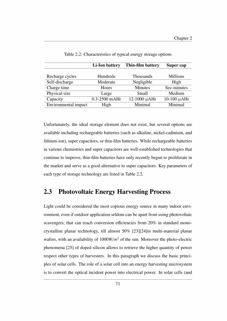
Chapter 2
Table 2.2: Characteristics of typical energy storage options
Li-Ion battery Thin-film battery Super cap
Recharge cycles Hundreds Thousands MillionsSelf-discharge Moderate Negligible HighCharge time Hours Minutes Sec-minutesPhysical size Large Small MediumCapacity 0.3-2500 mAHr 12-1000 µAHr 10-100 µAHrEnvironmental impact High Minimal Minimal
Unfortunately, the ideal storage element does not exist, but several options are
available including rechargeable batteries (such as alkaline, nickel-cadmium, and
lithium-ion), super capacitors, or thin-film batteries. While rechargeable batteries
in various chemistries and super capacitors are well-established technologies that
continue to improve, thin-film batteries have only recently begun to proliferate in
the market and serve as a good alternative to super capacitors. Key parameters of
each type of storage technology are listed in Table 2.2.
2.3 Photovoltaic Energy Harvesting Process
Light could be considered the most copious energy source in many indoor envi-
ronment, even if outdoor application seldom can be apart from using photovoltaic
scavengers, that can reach conversion efficiencies from 20% in standard mono-
crystalline planar technology, till almost 50% [23][24]in multi-material planar
wafers, with an availability of 1000W/m2 of the sun. Moreover the photo-electric
phenomena [25] of doped silicon allows to retrieve the higher quantity of power
respect other types of harvesters. In this paragraph we discuss the basic princi-
ples of solar cells. The role of a solar cell into an energy harvesting microsystem
is to convert the optical incident power into electrical power. In solar cells (and
71
Chapter 2
photodetectors) the optical energy is absorbed in a semiconductor and generates
excess of electron-hole pairs, producing photocurrents. The output terminal of a
solar cell is connected to a resistive load, so that the input optical power is con-
verted to electrical power. The simple p-n junction solar cell is considered in the
energy harvester integrated solution that will be described in this chapter. The
main characterization of a solar cell is made in terms of short circuit current, open
circuit voltage, maximum power and conversion efficiency.
2.3.1 Optical absorption
According to the wave-particle duality principle, the light wave can be treated
as particles, which are referred to as photons. The energy related to a photon is
E = hν where h is Plank’s constant and ν is the frequency. We can also relate
wavelength and energy by
λ =c
ν=
hc
E=
1.24E
µm (2.1)
where E is the photon energy in eV and c is the speed of light.
There are several possible photon-semiconductor interaction mechanisms. For
example, photons can interact with the semiconductor lattice whereby the photon
energy is converted into heat. Photons can also interact with the semiconductor
impurity atoms, either donors or acceptors, or they can interact with defects into
the semiconductor. However those kinds of interaction for an energy harvest-
ing application are undesired, and, so, are considered as source of efficiency loss
because any optical power related to those phenomena cannot be converted into
electrical power. The basic photon interaction process of greater interest is the in-
teraction with valence electrons. When a photon collides with a valence electron,
enough energy may be imparted to elevate the electron into conduction band. Such
a process generates electron-hole pairs and creates excess carrier concentrations.
72
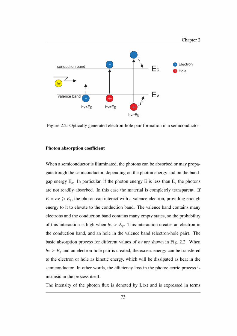
Chapter 2
hv
- +
-
+
-
Ev
Ecconduction band
valence band
- Electron+ Hole
hv<Eg hv=Eg
hv>Eg
Figure 2.2: Optically generated electron-hole pair formation in a semiconductor
Photon absorption coefficient
When a semiconductor is illuminated, the photons can be absorbed or may propa-
gate trough the semiconductor, depending on the photon energy and on the band-
gap energy Eg. In particular, if the photon energy E is less than Eg the photons
are not readily absorbed. In this case the material is completely transparent. If
E = hν > Eg, the photon can interact with a valence electron, providing enough
energy to it to elevate to the conduction band. The valence band contains many
electrons and the conduction band contains many empty states, so the probability
of this interaction is high when hv > Eg. This interaction creates an electron in
the conduction band, and an hole in the valence band (electron-hole pair). The
basic absorption process for different values of hv are shown in Fig. 2.2. When
hν > Eg and an electron-hole pair is created, the excess energy can be transfered
to the electron or hole as kinetic energy, which will be dissipated as heat in the
semiconductor. In other words, the efficiency loss in the photoelectric process is
intrinsic in the process itself.
The intensity of the photon flux is denoted by Iv(x) and is expressed in terms
73

Chapter 2
of energy/cm2-sec. If we assume that an incident photon flux at the position x
emerges at the position x + dx, it is possible to evaluate the absorbed energy per
unit time at the distance dx. In particular it is given by
αIν(x)dx (2.2)
where α is the absorption coefficient. The absorption coefficient is the relative
number of photons absorbed per unit distance, given in units of cm−1. In particu-
lar:
Iν(x + dx) − Iν(x) =dIν(x)
dx· dx = −αIν(x)dx (2.3)
ordIν(x)
dx= −αIν(x) (2.4)
If the initial condition is given as Iν(0) = Iν0, then the solution to the differential
equation (2.4) is
Iν(x) = Iν0e−αx (2.5)
The intensity of the photon flux decreases exponentially with the distance though
the semiconductor material. The photon intensity as a function of x for two general
values of absorption coefficient is shown in Fig. 2.3. If the absorption coefficient
is large, the photons are absorbed over a relatively short distance.
The absorption coefficient in the semiconductor is a very strong function of photon
energy and band-gap energy. The absorption coefficient increases very rapidly for
hν > Eg, or for λ < 1.24/Eg.
2.3.2 Solar cells
A solar cell is a p-n junction device with no voltage directly applied across the
junction. The solar cell converts photon power into electrical power and delivers
this power to a load. These devices have long been used for the power supply of
satellites and space vehicles, and also as the power supply to some calculators.
74
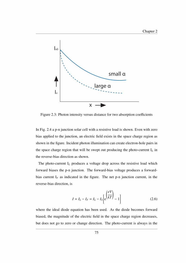
Chapter 2
small α
large α
Iv0
x
Iv
Figure 2.3: Photon intensity versus distance for two absorption coefficients
In Fig. 2.4 a p-n junction solar cell with a resistive load is shown. Even with zero
bias applied to the junction, an electric field exists in the space charge region as
shown in the figure. Incident photon illumination can create electron-hole pairs in
the space charge region that will be swept out producing the photo-current IL in
the reverse-bias direction as shown.
The photo-current IL produces a voltage drop across the resistive load which
forward biases the p-n junction. The forward-bias voltage produces a forward-
bias current IF as indicated in the figure. The net p-n junction current, in the
reverse-bias direction, is
I = IL − IF = IL − IS
[e
(eV
kT
)− 1
](2.6)
where the ideal diode equation has been used. As the diode becomes forward
biased, the magnitude of the electric field in the space charge region decreases,
but does not go to zero or change direction. The photo-current is always in the
75
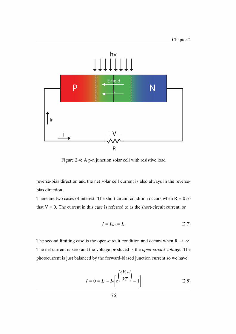
Chapter 2
P NE-field
IL
hv
+ V -
IF
I
R
Figure 2.4: A p-n junction solar cell with resistive load
reverse-bias direction and the net solar cell current is also always in the reverse-
bias direction.
There are two cases of interest. The short circuit condition occurs when R = 0 so
that V = 0. The current in this case is referred to as the short-circuit current, or
I = IS C = IL (2.7)
The second limiting case is the open-circuit condition and occurs when R → ∞.
The net current is zero and the voltage produced is the open-circuit voltage. The
photocurrent is just balanced by the forward-biased junction current so we have
I = 0 = IL − IS
[e
(eVOC
kT
)− 1
](2.8)
76

Chapter 2
ISC
VOCV
I
Figure 2.5: I-V characteristics of a p-n junction solar cell
thus the open-circuit voltage VOC is
VOC = Vt ln(1 +
IL
IS
)(2.9)
A plot of the diode current I as a function of the diode voltage V from equation
(2.6) is shown in Fig. 2.5. It is possible to note the short-circuit current and the
open-circuit voltage points on the curve. The power delivered to the resistive load
is
P = I ·V = IL ·V − IS
[e
(eVOC
kT
)− 1
]·V (2.10)
It is possible to find the current and the voltage which will deliver the maximum
power to the load by setting the derivative of P equal to zero, or dP/dV = 0. Using
equation (2.10), we find
dP
dV= 0 = IL − IS
[e
(eVOC
kT
)− 1
]− IS Vm
( e
kT
)e
(eVm
kT
)(2.11)
77

Chapter 2
ISC
VOCV
I
Im
Vm
Figure 2.6: Maximum power rectangle of the solar cell I-V characteristics
where Vm is the voltage which produces the maximum power. We can now rewrite
equation (2.11) in the form
(1 +
Vm
Vt
)e
(eVm
kT
)= 1 +
IL
IS(2.12)
The value of Vm may be determined by trial and error. Fig. 2.6 shows the maxi-
mum power rectangle where Im is the current when V = Vm.
2.4 Integrated Micro-Solar Cell Structures for Har-vesting Supplied Microsystems in 0.35-µm CMOSTechnology
In this section we present a solar harvester test chip, realized to characterize sev-
eral integrated solar cell structures, gathering the information required to design
a complete power management system for handling the harvested energy. In par-
ticular, we realized photodiodes with three different geometries of the p-diffusion,
and three different dimensions of the n-well. The chip is realized in a 0.35-µm
78
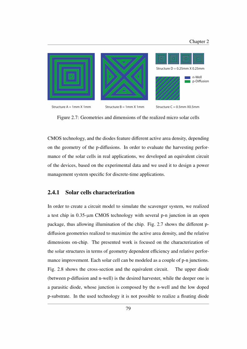
Chapter 2
Structure D = 0.25mm X 0.25mm
n-Wellp-Diffusion
Structure C = 0.5mm X0.5mmStructure B = 1mm X 1mmStructure A = 1mm X 1mm
Figure 2.7: Geometries and dimensions of the realized micro solar cells
CMOS technology, and the diodes feature different active area density, depending
on the geometry of the p-diffusions. In order to evaluate the harvesting perfor-
mance of the solar cells in real applications, we developed an equivalent circuit
of the devices, based on the experimental data and we used it to design a power
management system specific for discrete-time applications.
2.4.1 Solar cells characterization
In order to create a circuit model to simulate the scavenger system, we realized
a test chip in 0.35-µm CMOS technology with several p-n junction in an open
package, thus allowing illumination of the chip. Fig. 2.7 shows the different p-
diffusion geometries realized to maximize the active area density, and the relative
dimensions on-chip. The presented work is focused on the characterization of
the solar structures in terms of geometry dependent efficiency and relative perfor-
mance improvement. Each solar cell can be modeled as a couple of p-n junctions.
Fig. 2.8 shows the cross-section and the equivalent circuit. The upper diode
(between p-diffusion and n-well) is the desired harvester, while the deeper one is
a parasitic diode, whose junction is composed by the n-well and the low doped
p-substrate. In the used technology it is not possible to realize a floating diode
79
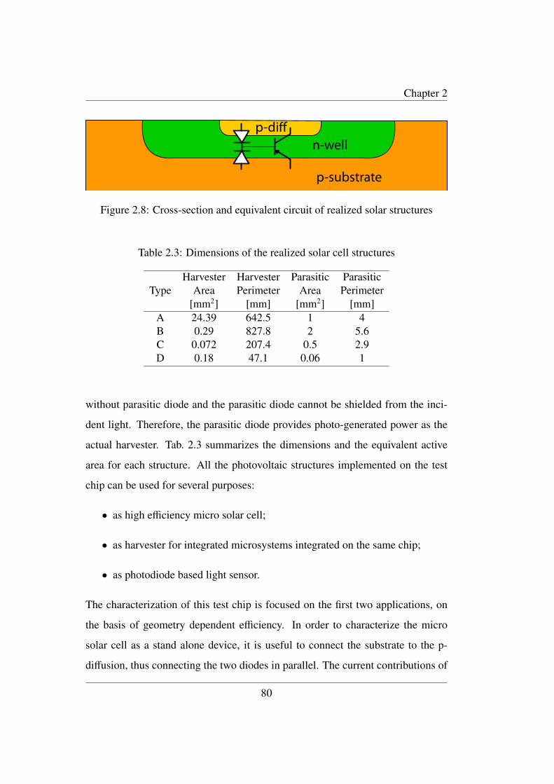
Chapter 2
p-substrate
n-wellp-di
Figure 2.8: Cross-section and equivalent circuit of realized solar structures
Table 2.3: Dimensions of the realized solar cell structures
TypeHarvester Harvester Parasitic Parasitic
Area Perimeter Area Perimeter[mm2] [mm] [mm2] [mm]
A 24.39 642.5 1 4B 0.29 827.8 2 5.6C 0.072 207.4 0.5 2.9D 0.18 47.1 0.06 1
without parasitic diode and the parasitic diode cannot be shielded from the inci-
dent light. Therefore, the parasitic diode provides photo-generated power as the
actual harvester. Tab. 2.3 summarizes the dimensions and the equivalent active
area for each structure. All the photovoltaic structures implemented on the test
chip can be used for several purposes:
• as high efficiency micro solar cell;
• as harvester for integrated microsystems integrated on the same chip;
• as photodiode based light sensor.
The characterization of this test chip is focused on the first two applications, on
the basis of geometry dependent efficiency. In order to characterize the micro
solar cell as a stand alone device, it is useful to connect the substrate to the p-
diffusion, thus connecting the two diodes in parallel. The current contributions of
80
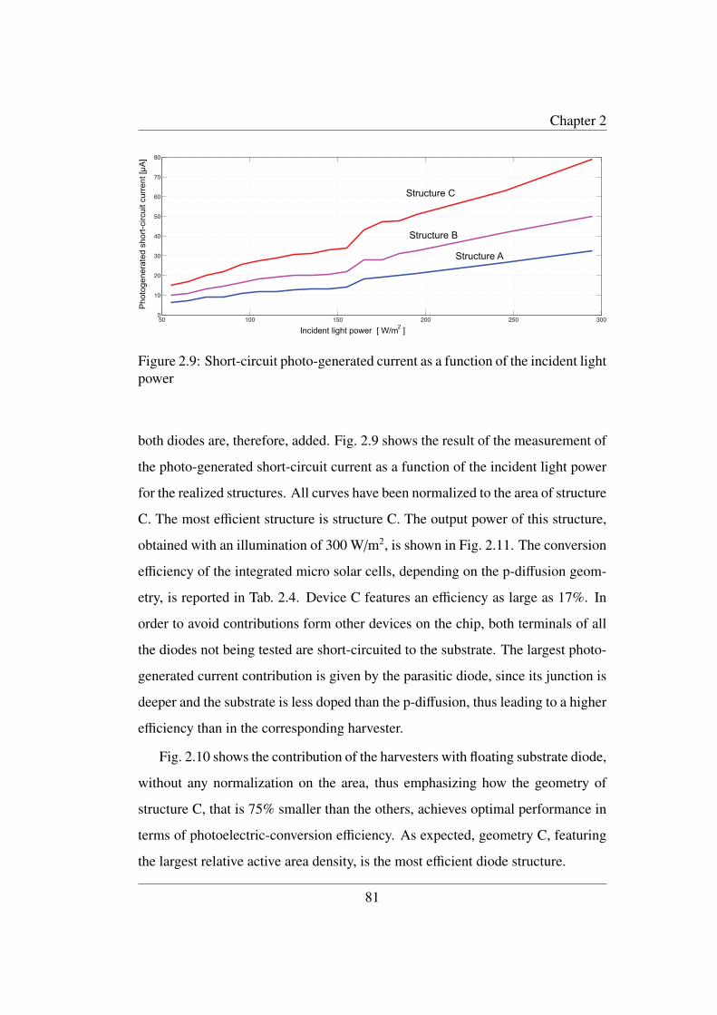
Chapter 2
50 100 150 200 250 3000
10
20
30
40
50
60
70
80
Structure C
Structure B
Structure A
Incident light power [ W/m ]2
Pho
toge
nera
ted
shor
t-circ
uit c
urre
nt [µ
A]
Figure 2.9: Short-circuit photo-generated current as a function of the incident lightpower
both diodes are, therefore, added. Fig. 2.9 shows the result of the measurement of
the photo-generated short-circuit current as a function of the incident light power
for the realized structures. All curves have been normalized to the area of structure
C. The most efficient structure is structure C. The output power of this structure,
obtained with an illumination of 300 W/m2, is shown in Fig. 2.11. The conversion
efficiency of the integrated micro solar cells, depending on the p-diffusion geom-
etry, is reported in Tab. 2.4. Device C features an efficiency as large as 17%. In
order to avoid contributions form other devices on the chip, both terminals of all
the diodes not being tested are short-circuited to the substrate. The largest photo-
generated current contribution is given by the parasitic diode, since its junction is
deeper and the substrate is less doped than the p-diffusion, thus leading to a higher
efficiency than in the corresponding harvester.
Fig. 2.10 shows the contribution of the harvesters with floating substrate diode,
without any normalization on the area, thus emphasizing how the geometry of
structure C, that is 75% smaller than the others, achieves optimal performance in
terms of photoelectric-conversion efficiency. As expected, geometry C, featuring
the largest relative active area density, is the most efficient diode structure.
81
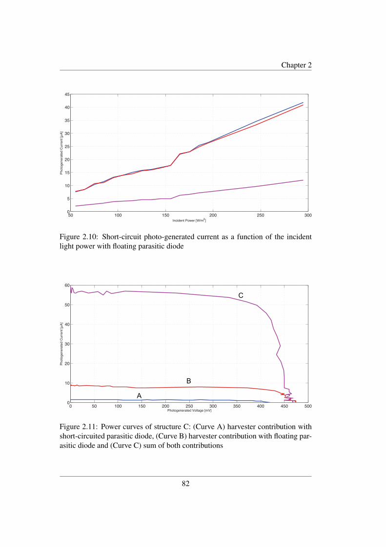
Chapter 2
50 100 150 200 250 3000
5
10
15
20
25
30
35
40
45
Incident Power [W/m2]
Pho
toge
nera
ted
Cur
rent
[µA
]
Figure 2.10: Short-circuit photo-generated current as a function of the incidentlight power with floating parasitic diode
0 50 100 150 200 250 300 350 400 450 5000
10
20
30
40
50
60
Photogenerated Voltage [mV]
Pho
toge
nera
ted
Cur
rent
[µA
]
A
B
C
Figure 2.11: Power curves of structure C: (Curve A) harvester contribution withshort-circuited parasitic diode, (Curve B) harvester contribution with floating par-asitic diode and (Curve C) sum of both contributions
82
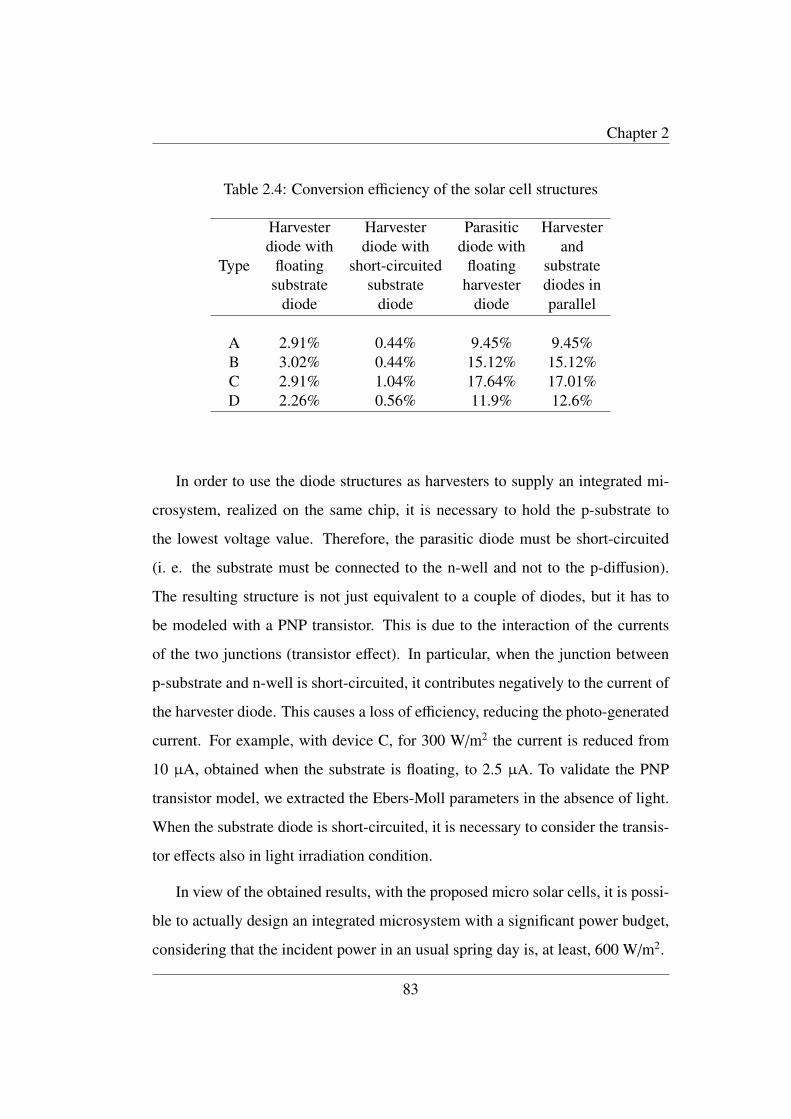
Chapter 2
Table 2.4: Conversion efficiency of the solar cell structures
Type
Harvester Harvester Parasitic Harvesterdiode with diode with diode with and
floating short-circuited floating substratesubstrate substrate harvester diodes in
diode diode diode parallel
A 2.91% 0.44% 9.45% 9.45%B 3.02% 0.44% 15.12% 15.12%C 2.91% 1.04% 17.64% 17.01%D 2.26% 0.56% 11.9% 12.6%
In order to use the diode structures as harvesters to supply an integrated mi-
crosystem, realized on the same chip, it is necessary to hold the p-substrate to
the lowest voltage value. Therefore, the parasitic diode must be short-circuited
(i. e. the substrate must be connected to the n-well and not to the p-diffusion).
The resulting structure is not just equivalent to a couple of diodes, but it has to
be modeled with a PNP transistor. This is due to the interaction of the currents
of the two junctions (transistor effect). In particular, when the junction between
p-substrate and n-well is short-circuited, it contributes negatively to the current of
the harvester diode. This causes a loss of efficiency, reducing the photo-generated
current. For example, with device C, for 300 W/m2 the current is reduced from
10 µA, obtained when the substrate is floating, to 2.5 µA. To validate the PNP
transistor model, we extracted the Ebers-Moll parameters in the absence of light.
When the substrate diode is short-circuited, it is necessary to consider the transis-
tor effects also in light irradiation condition.
In view of the obtained results, with the proposed micro solar cells, it is possi-
ble to actually design an integrated microsystem with a significant power budget,
considering that the incident power in an usual spring day is, at least, 600 W/m2.
83

Chapter 2
Micro Solar Cell Ring
Oscillator(OSC)
ChargePump
VphAuxiliary
MicroSolarCell
Cs
LDO
Hysteresis ComparatorUnbalanced Inverter LO
AD
Supply Switch
0-500mV
0-3.3V
3.8V - 4.3V
3.3V
Figure 2.12: Block diagram of the proposed system
2.4.2 Power management system chip
Since a solar energy scavenger is intrinsically a discrete-time power source, which
varies with the environmental conditions, photovoltaic systems need an energy
storage device and a power management system [26]. Fortunately, many appli-
cations, such as sensor network nodes [27, 28, 29, 30] or, in general wireless
embedded systems [31, 32] that operate in discrete-time regime, consume power
only during short time-slots [33]. In the system that is being presented, an inte-
grated miniaturized solar cell is used as energy source and a power management
system has been developed [32], to handle the collected energy. The block di-
agram of the system is shown in Fig. 2.12, where a generic sensor system has
been adopted as load [34]. The circuit elevates with a charge pump the voltage
produced by the miniaturized solar cell and charges an external capacitor, in or-
der to supply with 3.3 V through a linear voltage regulator (LDO) the load for a
given time-slot, in asynchronous discrete-time regime. The time-slots dedicated
to energy accumulation and system operation are established automatically by the
system. With this solution it is possible, by choosing the value of the capaci-
tance, to trade the amount of power available for the load with the time required
to accumulate it, thus allowing to supply the load for the required time-slot with
the required current with a given duty-cycle. The proposed power management
84
Chapter 2
circuit consists of an hysteresis comparator and an unbalanced inverter, that con-
trols a switch to connect the load to the storage capacitance. The comparator
monitors the charge voltage on the storage capacitor. When the stored charge
is sufficient to reach a voltage equal to 4.3 V the comparator provides a signal
that, by means of the unbalanced inverter, connects the LDO to the supply voltage
(i. e. the storage capacitor), thus supplying the load. When the voltage on the
storage capacitor decreases below 3.8 V, the LDO is disconnected and the load
switched off. In Section 2.4.1 we presented the solar source characterization of
the same structure implemented on this chip, used to design an equivalent circuit
described in Section 2.4.3. Those results are fundamental for the design of the
subsequent power management system. In Section 2.4.4 we describe the charge
pump used to elevate the solar cell voltage to a usable value, while Section 2.4.5
and Section 2.4.8 present the power management system and the LDO, respec-
tively. Finally, in Section 2.4.9 we derive the criteria for the choice of the value of
the storage capacitance.
2.4.3 Miniaturized solar cell model
On the basis of the results obtained from the characterization of the test chip, we
developed an equivalent circuit model of the solar cell implemented on the har-
vester chip. Fig. 2.11 shows the power curve used to create the equivalent circuit
model, illustrated in Fig. 2.13. In particular, by means of a Matlab algorithm
which needs only five measured values of the output power to find the appropriate
model parameters, we achieved the following result:
• Iph = 12.28 µA;
• AD = 100 µm2;
• PD = 40 µm;
85
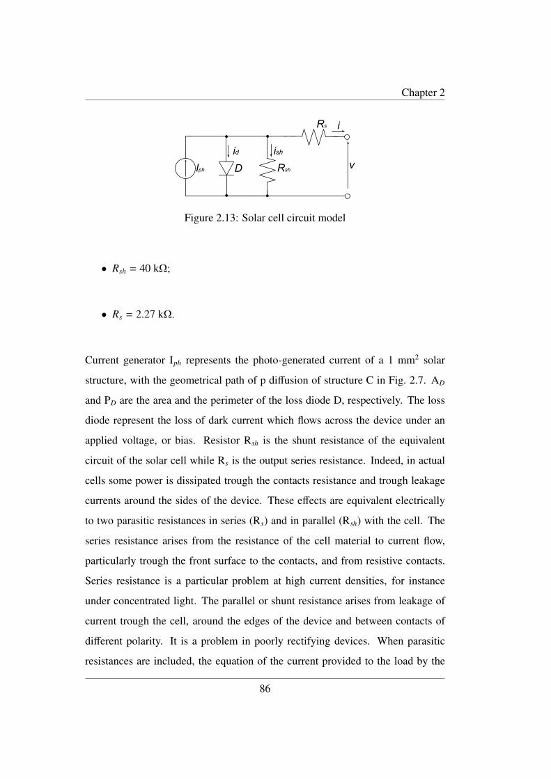
Chapter 2
Iph D Rsh
Rs i
vid ish
Figure 2.13: Solar cell circuit model
• Rsh = 40 kΩ;
• Rs = 2.27 kΩ.
Current generator Iph represents the photo-generated current of a 1 mm2 solar
structure, with the geometrical path of p diffusion of structure C in Fig. 2.7. AD
and PD are the area and the perimeter of the loss diode D, respectively. The loss
diode represent the loss of dark current which flows across the device under an
applied voltage, or bias. Resistor Rsh is the shunt resistance of the equivalent
circuit of the solar cell while Rs is the output series resistance. Indeed, in actual
cells some power is dissipated trough the contacts resistance and trough leakage
currents around the sides of the device. These effects are equivalent electrically
to two parasitic resistances in series (Rs) and in parallel (Rsh) with the cell. The
series resistance arises from the resistance of the cell material to current flow,
particularly trough the front surface to the contacts, and from resistive contacts.
Series resistance is a particular problem at high current densities, for instance
under concentrated light. The parallel or shunt resistance arises from leakage of
current trough the cell, around the edges of the device and between contacts of
different polarity. It is a problem in poorly rectifying devices. When parasitic
resistances are included, the equation of the current provided to the load by the
86

Chapter 2
ph
ph
ph
12
ph
1
M1
M2
M3
M4 M5
M6
C1 C2 C3
Mc
Mc1 Mc12 MoutVout
Cout
Cc
Cc1 Cc12
Three Stage Ring Oscillator
Charge Pump
Figure 2.14: Schematic of the ring oscillator and of the charge pump
cell becomes
ILOAD = Iph − I0
(e
q(V + IRs)kT − 1
)−
V + IRs
Rsh(2.13)
The output power curve of the created model is very close to the power curve of
the referred cell illuminated with an incident light power of 400 W/m2.
2.4.4 Ring oscillator and charge pump
The ring oscillator and the charge pump shown in Fig. 2.14 represent the front-
end block of the power management circuit. In order to allow the voltage across
the storage capacitor to reach at least 4 V, a Dickson charge pump [35] has been
implemented. The circuit requires two non-overlapping clock phases, ph and ph,
with amplitude equal to the voltage produced by the micro solar cell Vph. The
charge pump operates by moving charge along the diode chain, charging the ca-
pacitors to increasing voltages. The charge pump has been designed to obtained
a voltage of 5 V, starting from Vph 500 mV, thus requiring 12 stages. A three
stage ring oscillator provides the clock phases for the charge pump with a fre-
quency equal to 29.5 kHz, which correspond to the best trade-off between time
required to charge Cc and the charge transfer rate. The performance of the system
is limited by the supply voltage, which is equal to the open-circuit voltage Vph
87

Chapter 2
of the integrated micro solar cell, that forces all transistors to work in the sub-
threshold region. Such a system provides a very low current flow through each
transistor, introducing an efficiency loss in terms of charge transfer, and hence,
in terms of charging time. In order to provide a constant voltage of 3.3 V to the
load with a significant current for an established time slot, a storage capacitor is
necessary. Therefore, the proposed system is only suitable for loads operated in
discrete-time regime, such as sensor network nodes.
2.4.5 Power monitoring circuit
In order to control the voltage across the storage capacitor and hence the stored
energy, we developed a power monitoring circuit, which consists of an hysteresis
comparator and a voltage level shifter. The management circuit provides a control
signal to a switch, which connects the load to the storage capacitor when the
voltage across the storage capacitor reaches 4.3 V and disconnects the load when
it becomes lower than 3.8 V. In order to avoid discharging the storage capacitor,
the comparator is supplied directly by an auxiliary solar cell, while the inverter is
connected to the storage capacitor voltage. The total current consumption of the
monitoring block is less than 10 nA when the load is disconnected.
2.4.6 Hysteresis comparator
In order to control the charge and discharge status of the external capacitor, the
hysteresis comparator monitors the voltage on the capacitor, connects the load
when it reaches 4.3 V, and disconnect it when it decrease to 3.8 V. The schematic
of the comparator circuit is shown in Fig. 2.15. Hysteresis is required to have a
rising threshold different from the falling threshold. The hysteresis value of this
solution is proportional to the ratios βMP4/βMP3 and βMP5/βMP10. Assume that
initially the input voltage Vre f is much lower than the threshold voltage of the
88

Chapter 2
V
Vref
V Vout
R
Ma Mb
M1 M2
M3 M4 M5 M6
M7
M8
M9
M10
Vth_in
Figure 2.15: Schematic of the hysteresis comparator
comparator. In this case all the current flows through M1 and M4; M5 and M6
are off and consequently the output voltage is low. M3 is on too, but no current
is flowing in it. Initially when the input voltage increases nothing happens until
Vre f ' Vthin. At this point some current starts to flow into M2 from M3 and M1 and
IM1 starts to decrease. Therefore, the following relations can be written, assuming
αr as the ratio βM3/βM4 (footer r stands for rising):
IM2 = IM3 = αrIM4 (2.14)
IM1 + IM2 = IRbias (2.15)
IM1 + αrIM4 = IRbias (2.16)
IM2 = αrIM4 ∝ (Vre f − Vth−in)2 (2.17)
If the input voltage is increased further on, M2 demands for more current that can
come only from M3 that mirrors IM4 with the ratio αr, while IM4 is decreasing.
At a certain point, M3 ( αrIM4) cannot validate the equation (2.16), because IM3 =
IM1 is too low and consequently M3 goes on, providing the current M2 is asking,
given by
IM2 + IM3 = IRbias (2.18)
89
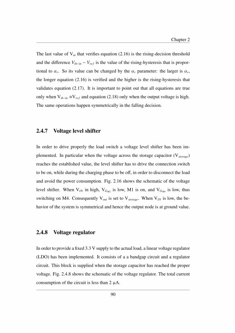
Chapter 2
The last value of Vin that verifies equation (2.16) is the rising-decision threshold
and the difference Vth−in − Vre f is the value of the rising-hysteresis that is propor-
tional to αr. So its value can be changed by the αr parameter: the larger is αr,
the longer equation (2.16) is verified and the higher is the rising-hysteresis that
validates equation (2.17). It is important to point out that all equations are true
only when Vth−in Vre f and equation (2.18) only when the output voltage is high.
The same operations happen symmetrically in the falling decision.
2.4.7 Voltage level shifter
In order to drive properly the load switch a voltage level shifter has been im-
plemented. In particular when the voltage across the storage capacitor (Vstorage)
reaches the established value, the level shifter has to drive the connection switch
to be on, while during the charging phase to be off, in order to disconnect the load
and avoid the power consumption. Fig. 2.16 shows the schematic of the voltage
level shifter. When VIN in high, VGM2 is low, M1 is on, and VGM4 is low, thus
switching on M4. Consequently Vout is set to Vstorage. When VIN is low, the be-
havior of the system is symmetrical and hence the output node is at ground value.
2.4.8 Voltage regulator
In order to provide a fixed 3.3 V supply to the actual load, a linear voltage regulator
(LDO) has been implemented. It consists of a a bandgap circuit and a regulator
circuit. This block is supplied when the storage capacitor has reached the proper
voltage. Fig. 2.4.8 shows the schematic of the voltage regulator. The total current
consumption of the circuit is less than 2 µA.
90
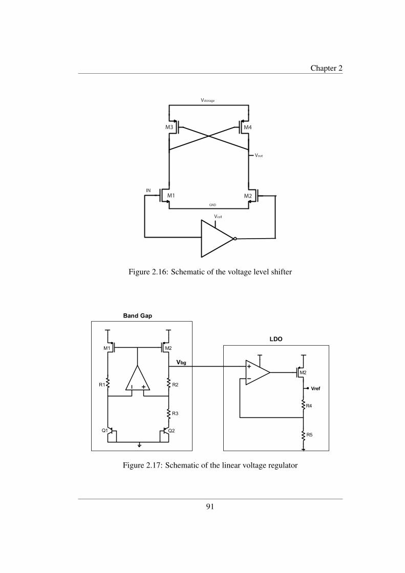
Chapter 2
Vcell
Vstorage
GND
IN
Vout
M1 M2
M3 M4
Figure 2.16: Schematic of the voltage level shifter
M1 M2
Q1 Q2
R1 R2
R3
Vbg
M2
R4
R5
Vref
Band Gap
LDO
Figure 2.17: Schematic of the linear voltage regulator
91

Chapter 2
Bandgap circuit
The bandgap circuit provides a stable voltage reference (Vbg) as reference input
of the LDO. It operates compensating the negative temperature coefficient of a
pn-junction voltage Vbe, with the positive temperature coefficient of the thermal
voltage VT . The output voltage of the circuit is
Vbg = Vbe + mVT (2.19)
where m depends on the bandgap circuit topology. With the topology used, m
coefficient is given by
m =R2
R1ln
[(W1/L1)(W2/L2)
A2
A1
](2.20)
Even if the supply voltage follows the discharge curve of the storage capacitor,
Vbg remains constant.
LDO
The LDO provides a stable 3.3 V supply voltage with an input voltage ranging
from 3.3 V to 4.8 V, allowing the actual load to operate properly. In particular, the
output voltage is given by
Vre f = VbgR4 + R5
R4. (2.21)
Simulation results demonstrate that the output voltage has a maximum error of
0.3% over the whole input voltage range, although, in order to reduce the power
dissipation, R4 and R5 are in the MΩ range. The total current consumption is about
1 µA.
2.4.9 Storage capacitor sizing
The storage capacitor is an external component, and, hence, its value can be cho-
sen on the basis of the actual load power consumption. In particular, the charge
transfer rate of the charge pump in the range from 3.8 V to 4.3 V is less than
92
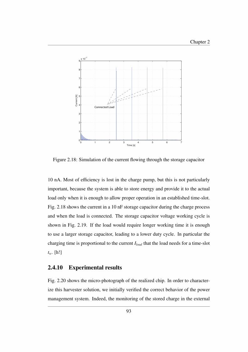
Chapter 2
0 1 2 3 4 5 6 70
1
2
3
4
5
6
7
8
9x 10
−7
Time [s]
Cur
rent
[A]
Connected Load
Figure 2.18: Simulation of the current flowing through the storage capacitor
10 nA. Most of efficiency is lost in the charge pump, but this is not particularly
important, because the system is able to store energy and provide it to the actual
load only when it is enough to allow proper operation in an established time-slot.
Fig. 2.18 shows the current in a 10 nF storage capacitor during the charge process
and when the load is connected. The storage capacitor voltage working cycle is
shown in Fig. 2.19. If the load would require longer working time it is enough
to use a larger storage capacitor, leading to a lower duty cycle. In particular the
charging time is proportional to the current Iload that the load needs for a time-slot
tw. [h!]
2.4.10 Experimental results
Fig. 2.20 shows the micro-photograph of the realized chip. In order to character-
ize this harvester solution, we initially verified the correct behavior of the power
management system. Indeed, the monitoring of the stored charge in the external
93
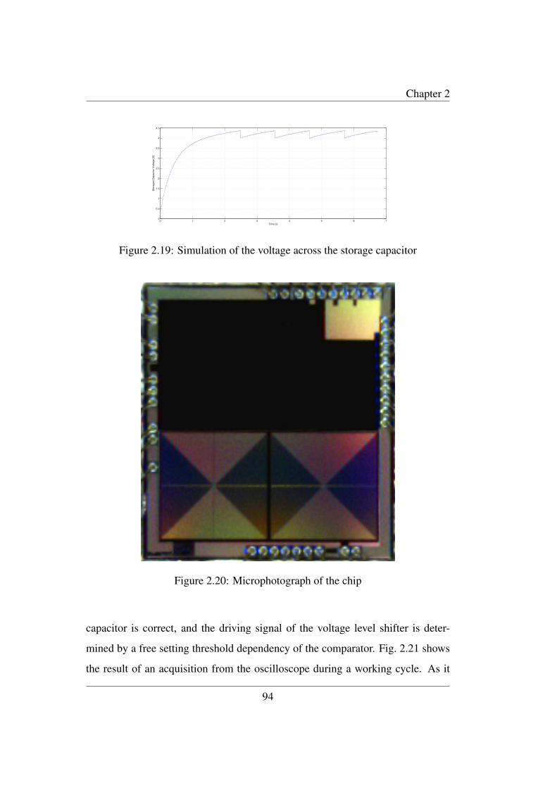
Chapter 2
0 1 2 3 4 5 6 70
0.5
1
1.5
2
2.5
3
3.5
4
4.5
Time [s]
Sto
rage
d C
apac
itor
Vol
tage
[V]
Figure 2.19: Simulation of the voltage across the storage capacitor
Figure 2.20: Microphotograph of the chip
capacitor is correct, and the driving signal of the voltage level shifter is deter-
mined by a free setting threshold dependency of the comparator. Fig. 2.21 shows
the result of an acquisition from the oscilloscope during a working cycle. As it
94
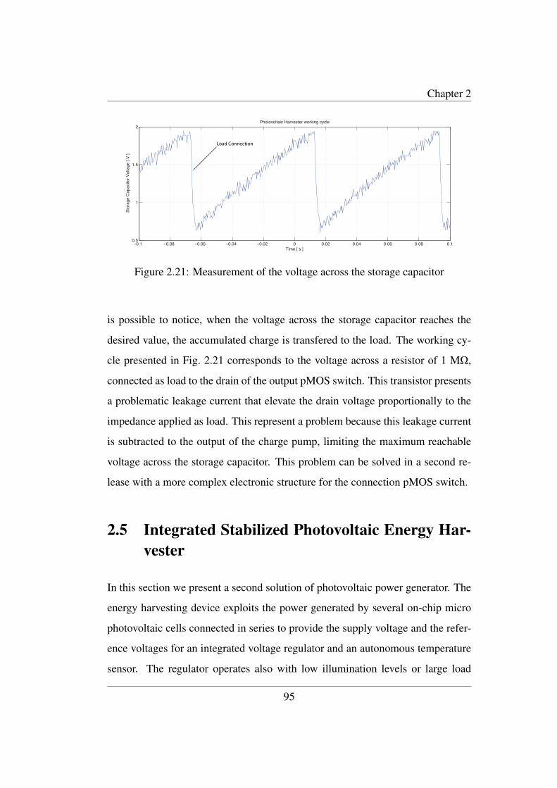
Chapter 2
−0.1 −0.08 −0.06 −0.04 −0.02 0 0.02 0.04 0.06 0.08 0.10.5
1
1.5
2
Time [ s ]
Sto
rage
Cap
acito
r V
olta
ge [
V ]
Photovoltaic Harvester working cycle
Load Connection
Figure 2.21: Measurement of the voltage across the storage capacitor
is possible to notice, when the voltage across the storage capacitor reaches the
desired value, the accumulated charge is transfered to the load. The working cy-
cle presented in Fig. 2.21 corresponds to the voltage across a resistor of 1 MΩ,
connected as load to the drain of the output pMOS switch. This transistor presents
a problematic leakage current that elevate the drain voltage proportionally to the
impedance applied as load. This represent a problem because this leakage current
is subtracted to the output of the charge pump, limiting the maximum reachable
voltage across the storage capacitor. This problem can be solved in a second re-
lease with a more complex electronic structure for the connection pMOS switch.
2.5 Integrated Stabilized Photovoltaic Energy Har-vester
In this section we present a second solution of photovoltaic power generator. The
energy harvesting device exploits the power generated by several on-chip micro
photovoltaic cells connected in series to provide the supply voltage and the refer-
ence voltages for an integrated voltage regulator and an autonomous temperature
sensor. The regulator operates also with low illumination levels or large load
95
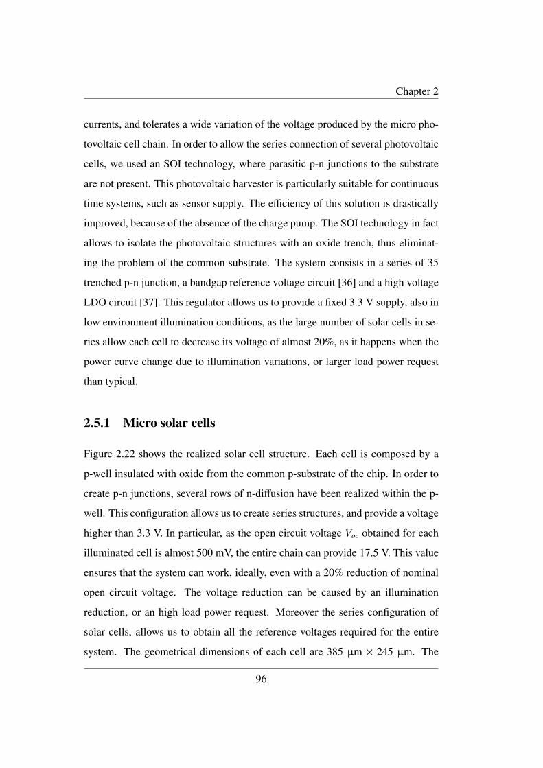
Chapter 2
currents, and tolerates a wide variation of the voltage produced by the micro pho-
tovoltaic cell chain. In order to allow the series connection of several photovoltaic
cells, we used an SOI technology, where parasitic p-n junctions to the substrate
are not present. This photovoltaic harvester is particularly suitable for continuous
time systems, such as sensor supply. The efficiency of this solution is drastically
improved, because of the absence of the charge pump. The SOI technology in fact
allows to isolate the photovoltaic structures with an oxide trench, thus eliminat-
ing the problem of the common substrate. The system consists in a series of 35
trenched p-n junction, a bandgap reference voltage circuit [36] and a high voltage
LDO circuit [37]. This regulator allows us to provide a fixed 3.3 V supply, also in
low environment illumination conditions, as the large number of solar cells in se-
ries allow each cell to decrease its voltage of almost 20%, as it happens when the
power curve change due to illumination variations, or larger load power request
than typical.
2.5.1 Micro solar cells
Figure 2.22 shows the realized solar cell structure. Each cell is composed by a
p-well insulated with oxide from the common p-substrate of the chip. In order to
create p-n junctions, several rows of n-diffusion have been realized within the p-
well. This configuration allows us to create series structures, and provide a voltage
higher than 3.3 V. In particular, as the open circuit voltage Voc obtained for each
illuminated cell is almost 500 mV, the entire chain can provide 17.5 V. This value
ensures that the system can work, ideally, even with a 20% reduction of nominal
open circuit voltage. The voltage reduction can be caused by an illumination
reduction, or an high load power request. Moreover the series configuration of
solar cells, allows us to obtain all the reference voltages required for the entire
system. The geometrical dimensions of each cell are 385 µm × 245 µm. The
96
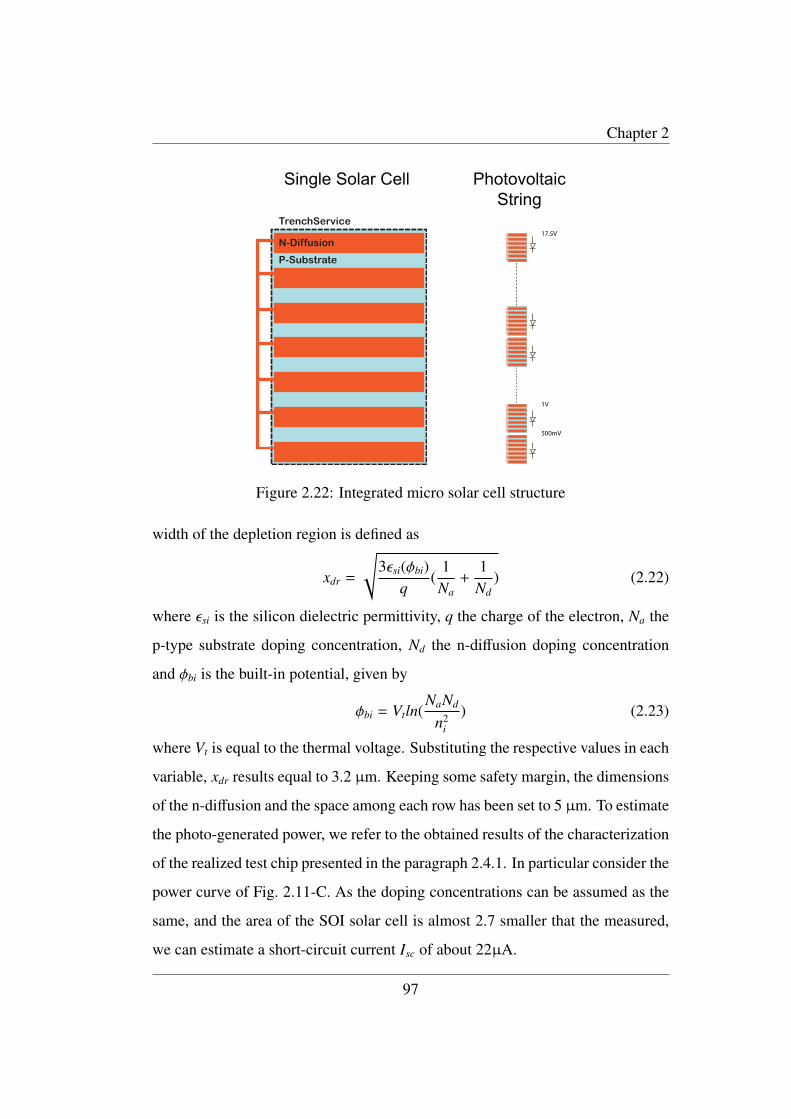
Chapter 2
N-Diffusion
P-Substrate
TrenchService
Single Solar Cell PhotovoltaicString
500mV
1V
17.5V
Figure 2.22: Integrated micro solar cell structure
width of the depletion region is defined as
xdr =
√3εsi(φbi)
q(
1Na
+1
Nd) (2.22)
where εsi is the silicon dielectric permittivity, q the charge of the electron, Na the
p-type substrate doping concentration, Nd the n-diffusion doping concentration
and φbi is the built-in potential, given by
φbi = Vtln(NaNd
n2i
) (2.23)
where Vt is equal to the thermal voltage. Substituting the respective values in each
variable, xdr results equal to 3.2 µm. Keeping some safety margin, the dimensions
of the n-diffusion and the space among each row has been set to 5 µm. To estimate
the photo-generated power, we refer to the obtained results of the characterization
of the realized test chip presented in the paragraph 2.4.1. In particular consider the
power curve of Fig. 2.11-C. As the doping concentrations can be assumed as the
same, and the area of the SOI solar cell is almost 2.7 smaller that the measured,
we can estimate a short-circuit current Isc of about 22µA.
97
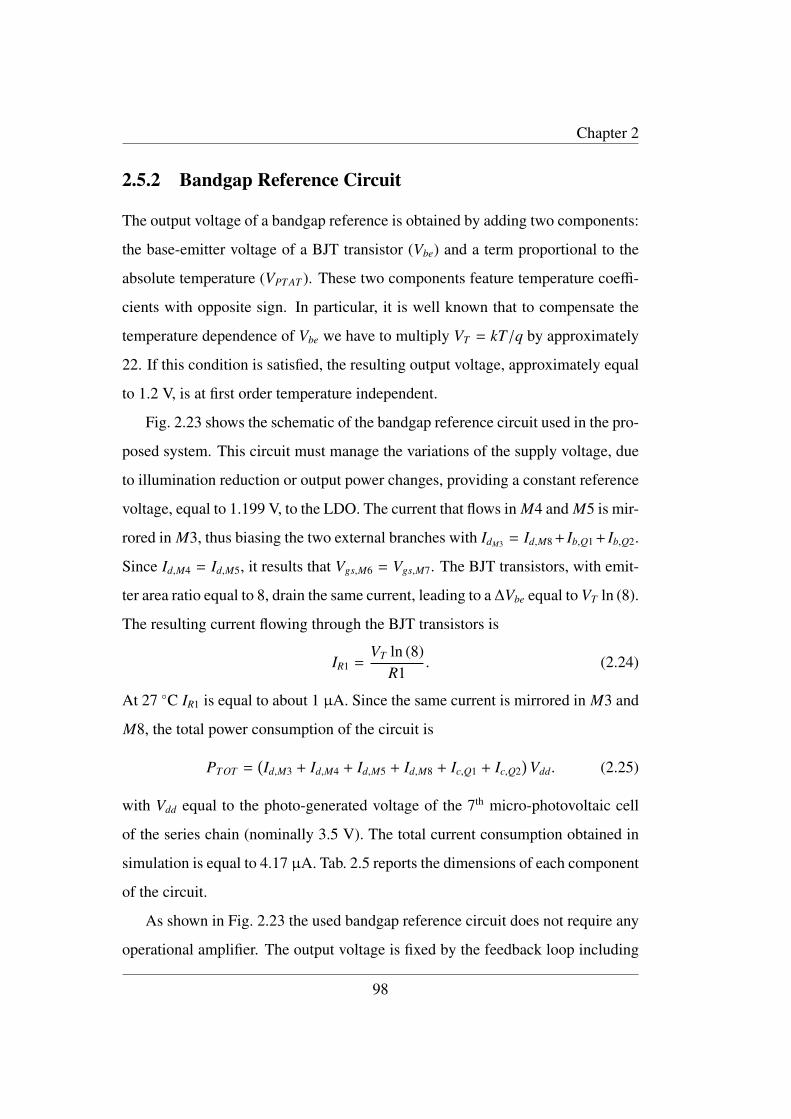
Chapter 2
2.5.2 Bandgap Reference Circuit
The output voltage of a bandgap reference is obtained by adding two components:
the base-emitter voltage of a BJT transistor (Vbe) and a term proportional to the
absolute temperature (VPT AT ). These two components feature temperature coeffi-
cients with opposite sign. In particular, it is well known that to compensate the
temperature dependence of Vbe we have to multiply VT = kT/q by approximately
22. If this condition is satisfied, the resulting output voltage, approximately equal
to 1.2 V, is at first order temperature independent.
Fig. 2.23 shows the schematic of the bandgap reference circuit used in the pro-
posed system. This circuit must manage the variations of the supply voltage, due
to illumination reduction or output power changes, providing a constant reference
voltage, equal to 1.199 V, to the LDO. The current that flows in M4 and M5 is mir-
rored in M3, thus biasing the two external branches with IdM3 = Id,M8 + Ib,Q1 + Ib,Q2.
Since Id,M4 = Id,M5, it results that Vgs,M6 = Vgs,M7. The BJT transistors, with emit-
ter area ratio equal to 8, drain the same current, leading to a ∆Vbe equal to VT ln (8).
The resulting current flowing through the BJT transistors is
IR1 =VT ln (8)
R1. (2.24)
At 27 C IR1 is equal to about 1 µA. Since the same current is mirrored in M3 and
M8, the total power consumption of the circuit is
PTOT =(Id,M3 + Id,M4 + Id,M5 + Id,M8 + Ic,Q1 + Ic,Q2
)Vdd. (2.25)
with Vdd equal to the photo-generated voltage of the 7th micro-photovoltaic cell
of the series chain (nominally 3.5 V). The total current consumption obtained in
simulation is equal to 4.17 µA. Tab. 2.5 reports the dimensions of each component
of the circuit.
As shown in Fig. 2.23 the used bandgap reference circuit does not require any
operational amplifier. The output voltage is fixed by the feedback loop including
98
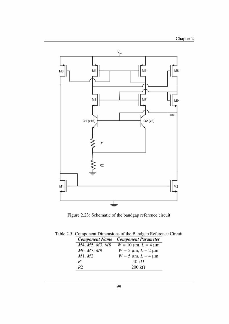
Chapter 2
Vdd
M6
5M4M
M7
M3 M8
M1 M2
R1
R2
M9
Q2 (x2)Q1 (x16)
OUT
Figure 2.23: Schematic of the bandgap reference circuit
Table 2.5: Component Dimensions of the Bandgap Reference CircuitComponent Name Component ParameterM4, M5, M3, M8 W = 10 µm, L = 4 µmM6, M7, M9 W = 5 µm, L = 2 µmM1, M2 W = 5 µm, L = 4 µmR1 40 kΩ
R2 200 kΩ
99
Chapter 2
Figure 2.24: Simulated temperature dependence of the bandgap reference voltage
transistor M8, which compensates any eventual variation of Vbe,Q1,Q2. The cascode
transistors M6 and M7 are used to increase the gain of the loop. Considering in
simulation a temperature ranging from −40 C to 150 C, the output voltage in
typical conditions shows a variation of 0.8 mV, corresponding to 3.5 ppm/C, as
illustrated in Fig. 2.24. In worst cases the variation of the output voltage ranges
from 6.6 mV to 8 mV (from 29 ppm/C to 35 ppm/C).
In order to emulate a reduction of the incident light power, we simulated the
bandgap reference circuit with a ramp applied to the power supply voltage Vdd,
finding the minimum micro-photovoltaic cell voltage required to start-up the cir-
cuit at different temperatures. The achieved results are summarized in Tab. 2.6.
In order to reduce the power consumption, current IdM3 is mirrored to bias also the
Table 2.6: Minimum Bandgap Reference Circuit Operating VoltageTemperature [C] Minimum Photovoltaic Cell Voltage [mV]
−40 365.427 362.4
150 352
LDO circuit.
100
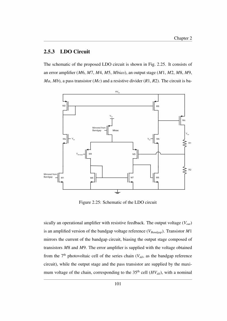
Chapter 2
2.5.3 LDO Circuit
The schematic of the proposed LDO circuit is shown in Fig. 2.25. It consists of
an error amplifier (M6, M7, M4, M5, Mbias), an output stage (M1, M2, M8, M9,
Ma, Mb), a pass transistor (Mc) and a resistive divider (R1, R2). The circuit is ba-
Mirrored fromBandgap
Mirrored fromBandgap
Vdd
HVdd
M2 M9
Ma Mb
Mc
M4 M5
M1 M6 M7 M8
R1
R2
Vout
VBandgap
Vdd Vdd
Mbias
Figure 2.25: Schematic of the LDO circuit
sically an operational amplifier with resistive feedback. The output voltage (Vout)
is an amplified version of the bandgap voltage reference (VBandgap). Transistor M1
mirrors the current of the bandgap circuit, biasing the output stage composed of
transistors M8 and M9. The error amplifier is supplied with the voltage obtained
from the 7th photovoltaic cell of the series chain (Vdd, as the bandgap reference
circuit), while the output stage and the pass transistor are supplied by the maxi-
mum voltage of the chain, corresponding to the 35th cell (HVdd), with a nominal
101

Chapter 2
Table 2.7: Component Dimensions of the LDO CircuitComponent Name Component ParameterM2, M9 W = 6 µm, L = 4 µmMa, Mb W = 6 µm, L = 2 µmMc W = 24 µm, L = 2 µmM1, M3 W = 10 µm, L = 4 µmM4, M5 W = 10 µm, L = 2 µmM6, M7 W = 4 µm, L = 4 µmM8 W = 0.5 µm, L = 0.35 µmR1 1 MΩ
R2 1.8 MΩ
value of 17.5 V. To protect M1 and M8 from the high voltage, we introduced a
cascode structure with the high-voltage transistors Ma and Mb.
The transfer function of the LDO circuit can be written as
Vout
VBandgap=
A1 − Aβ
, (2.26)
where
A = gm5 (rds5‖rds7) gm8rds9 (2.27)
and
β =R2
R1 + R2. (2.28)
Assuming Aβ 1, we obtain
Vout
VBandgap= 1 +
R2R1
= 2.8, (2.29)
and, hence, starting from a bandgap reference voltage of 1.2 V, we obtain an output
voltage equal to 3.3 V. Tab. 2.7 summarizes the dimensions of all the devices of
the proposed LDO circuit.
The total current consumption of the LDO circuit is 3.25 µA, while the total
power dissipation depends on the incident light.
102
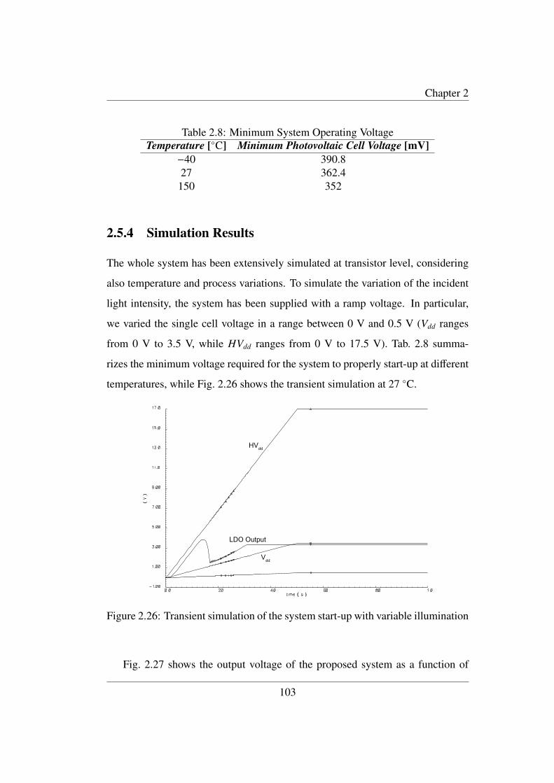
Chapter 2
Table 2.8: Minimum System Operating VoltageTemperature [C] Minimum Photovoltaic Cell Voltage [mV]
−40 390.827 362.4150 352
2.5.4 Simulation Results
The whole system has been extensively simulated at transistor level, considering
also temperature and process variations. To simulate the variation of the incident
light intensity, the system has been supplied with a ramp voltage. In particular,
we varied the single cell voltage in a range between 0 V and 0.5 V (Vdd ranges
from 0 V to 3.5 V, while HVdd ranges from 0 V to 17.5 V). Tab. 2.8 summa-
rizes the minimum voltage required for the system to properly start-up at different
temperatures, while Fig. 2.26 shows the transient simulation at 27 C.
HVdd
Vdd
LDO Output
Figure 2.26: Transient simulation of the system start-up with variable illumination
Fig. 2.27 shows the output voltage of the proposed system as a function of
103

Chapter 2
the temperature in the range from −40 C to 150 C. The overall output variation
results about 2.2 mV. The phase margin of the system results 75 with 10 pF of
Figure 2.27: System output voltage as a function of temperature
capacitive load.
Fig. 2.28 shows the layout of the chip. The total area is about 4.5 mm2, with
only 10% occupied by the electronics. Tab. 2.9 summarizes the simulated perfor-
Figure 2.28: Layout of the chip
mance of the system.
104

Chapter 2
Table 2.9: System PerformanceParameter ValuePSRR (DC) −130 dBPSRR (1 kHz) −82.6 dBPSRR (100 kHz) −42.9 dBPhase margin (10 pF load) 75
Bandgap current consumption 4.17 µABandgap temperature variation 800 µV (3.5 ppm/C)(−40 C – 150 C)LDO current consumption 3.25 µAOutput voltage temperature variation 2.2 mV (3.5 ppm/C)(−40 C – 150 C)Total current consumption 7.42 µAMinimum photovoltaic cell voltage (27 C) 362 mV
2.5.5 Temperature Sensor
In order to validate the adopted energy harvesting concept, we also implemented
on-chip a temperature sensor. To this end, the temperature dependent bias current
of the bandgap circuit has been mirrored in an additional branch. This current,
flowing through a resistor produces a temperature dependent voltage, as shown in
Fig. 2.29. The value of the sensing resistor is 6.8 MΩ, and the system has been
simulated in the temperature range from −40 C to 150 C.
2.5.6 Experimental Results
Fig. 2.30 shows the microphotograph of the implemented device. The total area
of the chip is about 4 mm2, and it has been fabricated with a 0.35-µm SOI CMOS
technology. The electronics has been shielded by a metal layer to avoid illumina-
tion, and it is represented by the matt rectangle on the left bottom side of Fig. 2.30.
Fig. 2.31 shows the power curve of a reference photovoltaic cell, obtained chang-
ing the load current value with a power of the incident constant spectrum light
equal to 300 W/m2. Fig. 2.32 shows the power curve on a resistive load applied to
105
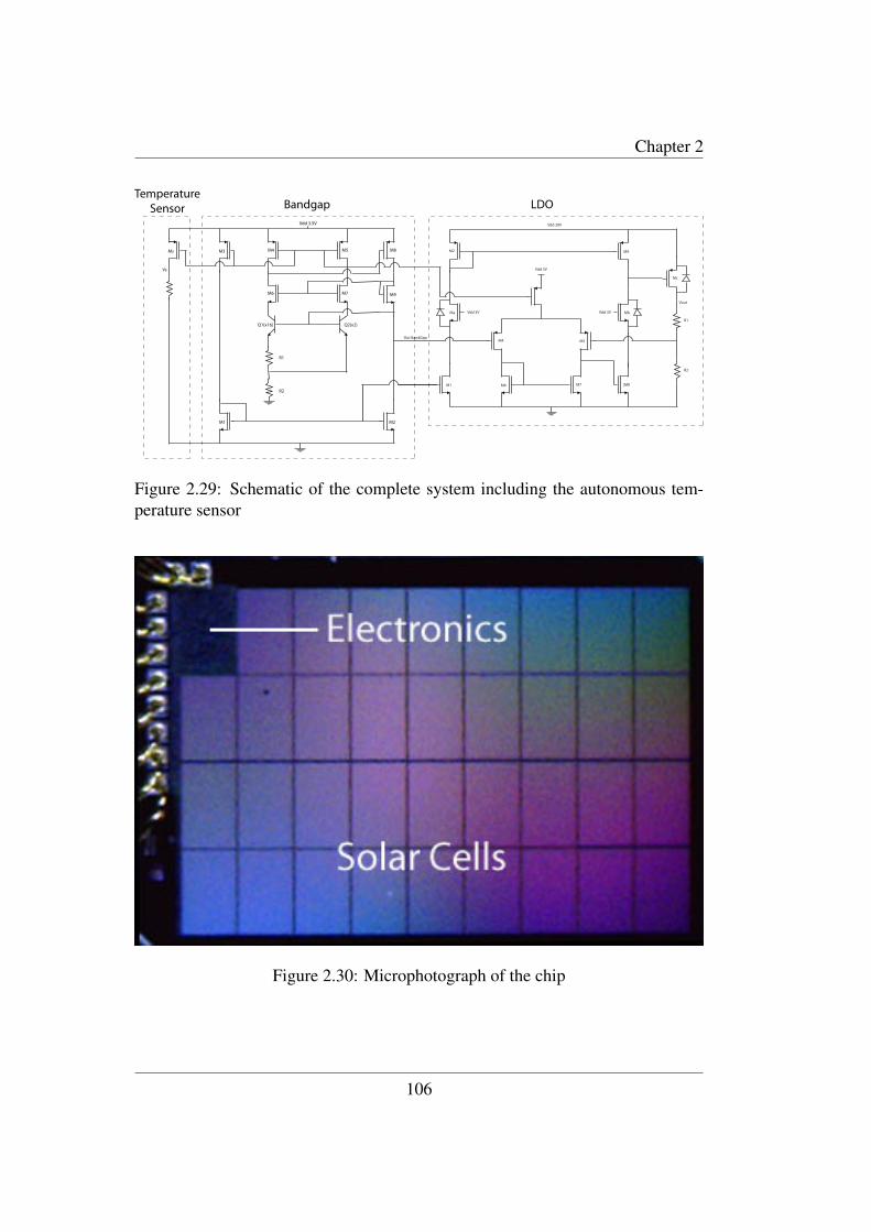
Chapter 2
Vdd 3.5V
M6
5M4M
M7
M3 M8
M1 M2
R1
R2
M9
)2x(2Q)61x(1Q
Out BandGap
Vdd 3V
V3 ddVV3 ddV
Vdd 20V
M2 M9
Ma Mb
Mc
M4 M5
M1 M6 M7 |M8
R1
R2
Vout
Bandgap LDO
Ms
Temperature
Sensor
Vs
Figure 2.29: Schematic of the complete system including the autonomous tem-perature sensor
Figure 2.30: Microphotograph of the chip
106
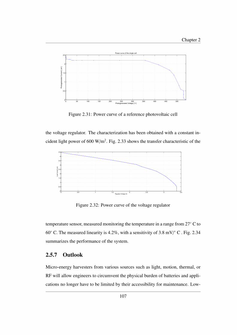
Chapter 2
0 50 100 150 200 250 300 350 400 450 5000
0.5
1
1.5
2
2.5
Photogenerated Voltage [ V ]
Pho
toge
nera
ted
Cur
rent
[ uA
]
Power curve of the single cell
Figure 2.31: Power curve of a reference photovoltaic cell
the voltage regulator. The characterization has been obtained with a constant in-
cident light power of 600 W/m2. Fig. 2.33 shows the transfer characteristic of the
0 0.5 1 1.5 2 2.5 3 3.50
0.5
1
1.5
2
2.5
3
3.5
4
4.5
Regulator Voltage (V)
Load
Cur
rent
(uA
)
Figure 2.32: Power curve of the voltage regulator
temperature sensor, measured monitoring the temperature in a range from 27 C to
60 C. The measured linearity is 4.2%, with a sensitivity of 3.8 mV/ C . Fig. 2.34
summarizes the performance of the system.
2.5.7 Outlook
Micro-energy harvesters from various sources such as light, motion, thermal, or
RF will allow engineers to circumvent the physical burden of batteries and appli-
cations no longer have to be limited by their accessibility for maintenance. Low-
107
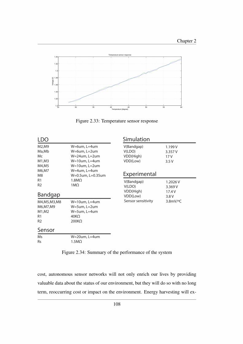
Chapter 2
25 30 35 40 45 50 55 601.2
1.22
1.24
1.26
1.28
1.3
1.32
1.34
Temperature [degree]
Vo
lta
ge
[V
]
Temperature sensor response
Figure 2.33: Temperature sensor response
M2,M9Ma,MbMcM1,M3M4,M5M6,M7M8R1R2
W=6um, L=4umW=6um, L=2umW=24um, L=2umW=10um, L=4umW=10um, L=2umW=4um, L=4umW=0.5um, L=0.35um1.8MΩ1MΩ
M4,M5,M3,M8M6,M7,M9M1,M2R1R2
W=10um, L=4umW=5um, L=2umW=5um, L=4um40KΩ200KΩ
MsRs
W=20um, L=4um1.5MΩ
Bandgap
Sensor
LDO SimulationV(Bandgap)V(LDO)VDD(High)VDD(Low)
1.199 V3.357 V17 V3.5 V
ExperimentalV(Bandgap)V(LDO)VDD(High)VDD(Low)Sensor sensitivity
1.2026 V3.369 V17.4 V3.8 V3.8mV/ºC
Figure 2.34: Summary of the performance of the system
cost, autonomous sensor networks will not only enrich our lives by providing
valuable data about the status of our environment, but they will do so with no long
term, reoccurring cost or impact on the environment. Energy harvesting will ex-
108

Chapter 2
tend the usable life of existing products and will enable design options that were
not possible before. Some applications may sound like science fiction today, but
the technology exists to enable a new generation of applications. By harvesting
the vibrational energy, intelligent sensors will be able to be implanted in roads,
bridges, and buildings at the time of construction, providing real-time feedback
on the structural integrity guaranteeing our safety. By harvesting energy from
the sun, farmers will be able to monitor the health of their crop using low-cost,
disposable sensors, producing greater crop yield with lower maintenance. By har-
vesting the heat from the skin, smart band-aids smaller than a quarter will be able
to monitor patient’s vital signs and transmit the information wirelessly to a cen-
tral medical base station, without having to tether a patient to a machine. We just
need to break the design engineer’s mold of what a traditional power source needs
to look like and embrace the benefits of perpetually powered energy harvesting
systems.
109


Appendix A
PIC 16F877 Datasheet
111

CONCLUSIONI
© 2001 Microchip Technology Inc. DS30292C-page 1
PIC16F87X
Devices Included in this Data Sheet:
Microcontroller Core Features:
• High performance RISC CPU• Only 35 single word instructions to learn
• All single cycle instructions except for program branches which are two cycle
• Operating speed: DC - 20 MHz clock inputDC - 200 ns instruction cycle
• Up to 8K x 14 words of FLASH Program Memory, Up to 368 x 8 bytes of Data Memory (RAM)Up to 256 x 8 bytes of EEPROM Data Memory
• Pinout compatible to the PIC16C73B/74B/76/77
• Interrupt capability (up to 14 sources)• Eight level deep hardware stack• Direct, indirect and relative addressing modes
• Power-on Reset (POR)• Power-up Timer (PWRT) and
Oscillator Start-up Timer (OST) • Watchdog Timer (WDT) with its own on-chip RC
oscillator for reliable operation• Programmable code protection• Power saving SLEEP mode
• Selectable oscillator options• Low power, high speed CMOS FLASH/EEPROM
technology• Fully static design• In-Circuit Serial Programming™ (ICSP) via two
pins• Single 5V In-Circuit Serial Programming capability
• In-Circuit Debugging via two pins• Processor read/write access to program memory• Wide operating voltage range: 2.0V to 5.5V
• High Sink/Source Current: 25 mA• Commercial, Industrial and Extended temperature
ranges• Low-power consumption:
- < 0.6 mA typical @ 3V, 4 MHz
- 20 μA typical @ 3V, 32 kHz- < 1 μA typical standby current
Pin Diagram
Peripheral Features:
• Timer0: 8-bit timer/counter with 8-bit prescaler• Timer1: 16-bit timer/counter with prescaler,
can be incremented during SLEEP via external crystal/clock
• Timer2: 8-bit timer/counter with 8-bit periodregister, prescaler and postscaler
• Two Capture, Compare, PWM modules- Capture is 16-bit, max. resolution is 12.5 ns- Compare is 16-bit, max. resolution is 200 ns
- PWM max. resolution is 10-bit• 10-bit multi-channel Analog-to-Digital converter• Synchronous Serial Port (SSP) with SPI™ (Master
mode) and I2C™ (Master/Slave)• Universal Synchronous Asynchronous Receiver
Transmitter (USART/SCI) with 9-bit address detection
• Parallel Slave Port (PSP) 8-bits wide, withexternal RD, WR and CS controls (40/44-pin only)
• Brown-out detection circuitry forBrown-out Reset (BOR)
• PIC16F873• PIC16F874
• PIC16F876• PIC16F877
RB7/PGDRB6/PGC
RB5
RB4RB3/PGM
RB2
RB1
RB0/INT
VDD
VSS
RD7/PSP7
RD6/PSP6RD5/PSP5
RD4/PSP4
RC7/RX/DT
RC6/TX/CK
RC5/SDO
RC4/SDI/SDARD3/PSP3
RD2/PSP2
MCLR/VPP
RA0/AN0
RA1/AN1RA2/AN2/VREF-
RA3/AN3/VREF+
RA4/T0CKI
RA5/AN4/SS
RE0/RD/AN5
RE1/WR/AN6
RE2/CS/AN7VDD
VSS
OSC1/CLKIN
OSC2/CLKOUT
RC0/T1OSO/T1CKI
RC1/T1OSI/CCP2
RC2/CCP1
RC3/SCK/SCLRD0/PSP0
RD1/PSP1
1
2
3
4
5
6
7
8
910
11
12
13
14
15
16
17
18
1920
40
39
38
37
36
35
34
33
3231
30
2928
27
26
25
24
23
2221
PIC
16F
877/
874
PDIP
112

Conclusions
In this thesis we have presented the design of integrated magnetic sensor interface
circuits and photovoltaic energy harvesting solutions.
Initially, we realized an automated measurement setup to improve the reliability
of the result obtained with different approaches in the characterization of Fluxgate
magnetic sensors. The performance of the system has been improved by more then
50%. Then a new Fluxgate magnetic sensor interface circuit has been designed.
Special care has been taken in order to reduce the total power consumption, as the
final portable application is a current measurement system with digital output.
The energy harvesting solutions that has been proposed are suitable for discrete
and continuous time working systems. The first is a sort of solar battery with
a power management system, and the second is a photovoltaic voltage regulator
with an autonomous temperature sensor. All the obtained results have been pub-
lished in national and international conferences. The details of the publications
can be found at http://sms.unipv.it/%7emferri.
113


Bibliography
[1] R. Boll and K. Overshott, Magnetic Sensors, Volume 5, Sensors: A Compre-
hensive Survey. Wiley-VCH, 12 1989.
[2] P. Ripka and P. Navatril, “Fluxgate sensors for magnetopneumometry,” in
Proceedings of Sensors and Actuators A: Physical, vol. 60, May 1997, pp.
76–79.
[3] W. Hernandez, “Fluxgate magnetometer for magnetic fields in the range 1-
100 I14 t,” Electronics Letters, vol. 31, no. 24, pp. 2110–2111, Nov 1995.
[4] P. M. Drljaca, P. Kejik, F. Vincent, D. Piguet, and R. S. Popovic, “Low-power
2D fully integrated CMOS fluxgate magnetometer,” IEEE Sensors Journal,
vol. 5, pp. 909–915, Oct. 2005.
[5] S. Choi, S. Kawahito, Y. Matsumoto, M. Ispida, and Y. Tadokoro, “An inte-
grated micro fluxgate magnetic sensor,” Sensors and Actuators A: Physical,
vol. 55, pp. 121–126, July 1996.
[6] L. Chiesi, P. Kejik, B. Janossy, and R. Popovic, “CMOS planar 2D micro-
fluxgate sensor,” Sensors and Actuators A: Physical, vol. 82, pp. 174–180,
May 2000.
115
CONCLUSIONI
[7] A. Baschirotto, E. Dallago, M. Ferri, P. Malcovati, A. Rossini, and
G. Venchi, “A cmos 2d micro-fluxgate earth magnetic field detecting sys-
tem with rs232 digital output,” in IEEE Sensors, 2007, pp. 240 – 243.
[8] A. Baschirotto, E. Dallago, P. Malcovati, M. Marchesi, and G. Venchi, “De-
velopment and comparative analysis of fluxgate magnetic sensor structures
in pcb technology,” Magnetics, IEEE Transactions on, vol. 42, no. 6, pp.
1670–1680, June 2006.
[9] J.-S. Hwang, H.-S. Park, D.-S. Shim, K.-W. Na, W.-Y. Choi, and S.-O.
Choi, “Electronic compass using two-axis micro fluxgate sensing element,”
TRANSDUCERS, Solid-State Sensors, Actuators and Microsystems, 12th In-
ternational Conference on, 2003, vol. 2, pp. 1618–1621 vol.2, June 2003.
[10] A. Baschirotto, E. Dallago, P. Malcovati, M. Marchesi, and G. Venchi,
“From a pcb fluxgate to an integrated micro fluxgate magnetic sensor,” In-
strumentation and Measurement Technology Conference, 2005. IMTC 2005.
Proceedings of the IEEE, vol. 3, pp. 1756–1760, May 2005.
[11] A. Baschirotto, A. Cabrini, E. Dallago, P. Malcovati, M. Marchesi, and
G. Venchi, “Development and analysis of a pcb vector 2-d magnetic field
sensor system for electronic compasses,” Sensors Journal, IEEE, vol. 6,
no. 2, pp. 365–371, April 2006.
[12] A. Baschirotto, E. Dallago, V. Ferragina, M. Ferri, M. Grassi, P. Malcovati,
M. Marchesi, E. Melissano, M. Morelli, A. Rossini, S. Ruzza, P. Siciliano,
and G. Venchi, “A CMOS 2D micro-fluxgate earth magnetic field sensor
with digital output,” in IEEE International Solid-State Circuits Conference
Digest of Technical Papers, Feb. 2007, pp. 390–391.
116

CONCLUSIONI
[13] V. Ferragina, M. Ferri, M. Grassi, A. Rossini, P. Malcovati, and A. Baschi-
rotto, “A 12.4 enob incremental a/d converter for high-linearity sensors read-
out applications,” Circuits and Systems, 2007. ISCAS 2007. IEEE Interna-
tional Symposium on, pp. 3582–3585, May 2007.
[14] A. Baschirotto, F. Borghetti, E. Dallago, P. Malcovati, M. Marchesi, and
G. Venchi, “A cmos front-end circuit for integrated fluxgate magnetic sen-
sors,” in Circuits and Systems, 2006. ISCAS 2006. Proceedings. 2006 IEEE
International Symposium on, 0-0 2006, pp. 4 pp.–4406.
[15] A. Baschirotto, F. Borghetti, E. Dallago, P. Malcovati, M. March-
esi, E. Melissano, P. Siciliano, and G. Venchi, “Fluxgate magnetic
sensor and front-end circuitry in an integrated microsystem,” Sen-
sors and Actuators A: Physical, vol. 132, no. 1, pp. 90 –
97, 2006, the 19th European Conference on Solid-State Transducers.
[Online]. Available: http://www.sciencedirect.com/science/article/B6THG-
4K4WMR5-2/2/2fdffebb442ba7bf0d7f0b535013ea15
[16] E. Dallago, M. Ferri, P. Malcovati, A. Rossini, G. Venchi, and A. Baschi-
rotto, “A cmos 2d micro-fluxgate earth magnetic field detecting system with
rs232 digital output,” Sensors, 2007 IEEE, pp. 240–243, Oct. 2007.
[17] A. Baschirotto, E. Dallago, V. Ferragina, M. Ferri, M. Grassi, P. Malcovati,
M. Marchesi, E. Melissano, M. Morelli, A. Rossini, S. Ruzza, P. Siciliano,
and G. Venchi, “A cmos 2d micro-fluxgate earth magnetic field sensor with
digital output,” Solid-State Circuits Conference, 2007. ISSCC 2007. Digest
of Technical Papers. IEEE International, pp. 390–610, Feb. 2007.
[18] M. Marwick and A. Andreou, “Photo-battery fabricated in silicon on sap-
phire cmos,” Electronics Letters, vol. 44, no. 12, pp. 766–767, 5 2008.
117
CONCLUSIONI
[19] D. Dondi, D. Brunelli, L. Benini, P. Pavan, A. Bertacchini, and L. Larcher,
“Photovoltaic cell modeling for solar energy powered sensor networks,” Ad-
vances in Sensors and Interface, 2007. IWASI 2007. 2nd International Work-
shop on, pp. 1–6, June 2007.
[20] N. Guilar, A. Chen, T. Kleeburg, and R. Amirtharajah, “Integrated solar
energy harvesting and storage,” Low Power Electronics and Design, 2006.
ISLPED’06. Proceedings of the 2006 International Symposium on, pp. 20–
24, Oct. 2006.
[21] N. J. Guilar, E. G. Fong, T. Kleeburg, D. R. Yankelevich, and R. Amirthara-
jah, “Energy harvesting photodiodes with integrated 2d diffractive storage
capacitance,” in ISLPED ’08: Proceeding of the thirteenth international
symposium on Low power electronics and design. New York, NY, USA:
ACM, 2008, pp. 63–68.
[22] A. Hande, T. Polk, W. Walker, and D. Bhatia, “Indoor solar energy
harvesting for sensor network router nodes,” Microprocessors and
Microsystems, vol. 31, no. 6, pp. 420–432, September 2007. [Online].
Available: http://dx.doi.org/10.1016/j.micpro.2007.02.006
[23] A. Barnett, C. Honsberg, D. Kirkpatrick, S. Kurtz, D. Moore, D. Salzman,
R. Schwartz, J. Gray, S. Bowden, K. Goossen, M. Haney, D. Aiken, M. Wan-
lass, and K. Emery, “50Photovoltaic Energy Conversion, Conference Record
of the 2006 IEEE 4th World Conference on, vol. 2, pp. 2560–2564, May
2006.
[24] E. Ralph, “High efficiency solar cell arrays system trade-offs,” Photovoltaic
Energy Conversion, 1994., Conference Record of the Twenty Fourth. IEEE
118
CONCLUSIONI
Photovoltaic Specialists Conference - 1994, 1994 IEEE First World Confer-
ence on, vol. 2, pp. 1998–2001 vol.2, Dec 1994.
[25] J. McGee, “Photoelectric cells-a review of progress,” Component Parts, IRE
Transactions on, vol. 5, no. 1, pp. 2–23, Mar 1958.
[26] N. Guilar, A. Chen, T. Kleeburg, and R. Amirtharajah, “Integrated solar en-
ergy harvesting and storage,” in ACM/IEEE ISLPED, 2006, pp. 20–24.
[27] A. Kansal and M. Srivastava, “An environmental energy harvesting frame-
work for sensor networks,” in Intl. Symp. Low Power Elec. and Design
(ISLPED) ’03, 2003, pp. 481–486.
[28] A. Arms, C. Townsed, D. Churchill, J. Galbreath, and S. Mundell, “Power
management for energy harvesting wireless sensor,” in SPIE International
Symposium on Smart Structures and Smart Materials, 2005.
[29] B. Otis, Y. Chee, and J. Rabey, “A 400 µw-rx, 1.6mw-tx super-regenerative
transceiver for wireless sensor networks,” in IEEE International Solid-State
Circuits Conference (ISSCC 2005), 2005, pp. 396–7.
[30] M. Rahimi, H. Shah, G. Sukhatme, J. Heideman, and D. Estrin, “Studying
the feasibility of energy scavenging in mobile sensor network,” in IEEE In-
ternational Conference on Robotics and Automation Proceedings, 2003, pp.
19–24.
[31] V. Raghunathan, A. Kansal, J. Hsu, J. Friedman, and M. Srivastava, “De-
sign considerations for solar energy harvesting wireless embedded systems,”
in International Symposium on Informatic Processing in Sensor Networks,
2005, pp. 457–462.
119
CONCLUSIONI
[32] A. Kansal, J. Hsu, M. Srivastava, and V. Raqhunathan, “Harvesting aware
power management for sensor networks,” in ACM/IEEE Design Automation
Conference, 2006, pp. 651–656.
[33] W. Walker, T. Polk, A. Hande, and D. Bhatia, “Remote blood pressure mon-
itoring using a wireless sensor network,” in Sixth IEEE Annual Emerging
Information Technology Conference Proceedings, Dallas, Texas, 2006.
[34] P. Woias, Y. Manoli, T. Nann, and V. Stetten, “Energy harvesting for au-
tonomous microsystems,” in MST News, vol. 4, no. 05, 2005, pp. 42–45.
[35] J. Dickson, “On-chip high-voltage generation in nmos integrated circuits us-
ing an improved voltage multiplier technique,” in IEEE J. Solid-State Cir-
cuits Conference, vol. 11, no. 6, 1976, pp. 347–348.
[36] P. Malcovati, F. Maloberti, M. Pruzzi, and C. Fiocchi, “Curvature compen-
sated bicmos bandgap with 1 v supply voltage,” in Solid-State Circuits Con-
ference, 2000. ESSCIRC ’00. Proceedings of the 26th European, Sept. 2000,
pp. 7–10.
[37] C.-W. Lin and Y.-J. Liu, “A power efficient and fast transient response low
drop-out regulator in standard cmos process,” in VLSI Design, Automation
and Test, 2006 International Symposium on, April 2006, pp. 1–4.
120


