
Document Number: 319970-007
Intel® 4 Series Chipset Family Datasheet
For the Intel® 82Q45, 82Q43, 82B43, 82G45, 82G43, 82G41 Graphics and Memory Controller Hub (GMCH) and the Intel® 82P45, 82P43 Memory Controller Hub (MCH)
March 2010

2 Datasheet
INFORMATION IN THIS DOCUMENT IS PROVIDED IN CONNECTION WITH INTEL® PRODUCTS. NO LICENSE, EXPRESS OR IMPLIED, BY ESTOPPEL OR OTHERWISE, TO ANY INTELLECTUAL PROPERTY RIGHTS IS GRANTED BY THIS DOCUMENT. EXCEPT AS PROVIDED IN INTEL'S TERMS AND CONDITIONS OF SALE FOR SUCH PRODUCTS, INTEL ASSUMES NO LIABILITY WHATSOEVER, AND INTEL DISCLAIMS ANY EXPRESS OR IMPLIED WARRANTY, RELATING TO SALE AND/OR USE OF INTEL PRODUCTS INCLUDING LIABILITY OR WARRANTIES RELATING TO FITNESS FOR A PARTICULAR PURPOSE, MERCHANTABILITY, OR INFRINGEMENT OF ANY PATENT, COPYRIGHT OR OTHER INTELLECTUAL PROPERTY RIGHT. Intel products are not intended for use in medical, life saving, life sustaining, critical control or safety systems, or in nuclear facility applications.
Intel may make changes to specifications and product descriptions at any time, without notice.
Designers must not rely on the absence or characteristics of any features or instructions marked "reserved" or "undefined." Intel reserves these for future definition and shall have no responsibility whatsoever for conflicts or incompatibilities arising from future changes to them.
The Intel® 4 Series Chipset family may contain design defects or errors known as errata, which may cause the product to deviate from published specifications. Current characterized errata are available on request.
Contact your local Intel sales office or your distributor to obtain the latest specifications and before placing your product order.
I2C is a two-wire communications bus/protocol developed by Philips. SMBus is a subset of the I2C bus/protocol and was developed by Intel. Implementations of the I2C bus/protocol may require licenses from various entities, including Philips Electronics N.V. and North American Philips Corporation.
Intel® Active Management Technology requires the platform to have an Intel® AMT-enabled chipset, network hardware and software, connection with a power source and a network connection.
No computer system can provide absolute security under all conditions. Intel® Trusted Execution Technology (Intel® TXT) is a security technology under development by Intel and requires for operation a computer system with Intel® Virtualization Technology, a Intel® Trusted Execution Technology-enabled Intel processor, chipset, BIOS, Authenticated Code Modules, and an Intel or other Intel® Trusted Execution Technology compatible measured virtual machine monitor. In addition, Intel® Trusted Execution Technology requires the system to contain a TPMv1.2 as defined by the Trusted Computing Group and specific software for some uses.
Intel® Virtualization Technology requires a computer system with an enabled Intel® processor, BIOS, virtual machine monitor (VMM) and, for some uses, certain computer system software enabled for it. Functionality, performance or other benefits will vary depending on hardware and software configurations and may require a BIOS update. Software applications may not be compatible with all operating systems. Please check with your application vendor.
Intel, Pentium, Intel Core, and the Intel logo are trademarks of Intel Corporation in the U.S. and other countries.
*Other names and brands may be claimed as the property of others.
Copyright© 2010, Intel Corporation

Datasheet 3
Contents
1 Introduction ............................................................................................................ 211.1 Terminology ..................................................................................................... 271.2 (G)MCH System Overview .................................................................................. 30
1.2.1 Host Interface........................................................................................ 301.2.2 System Memory Interface ....................................................................... 311.2.3 Direct Media Interface (DMI).................................................................... 311.2.4 Multiplexed PCI Express* Graphics Interface and Intel® sDVO/DVI/HDMI/DP
Interface............................................................................................... 321.2.4.1 PCI Express* Interface .............................................................. 321.2.4.2 sDVO Multiplexed Interface (Intel® 82Q45, 82Q43, 82B43, 82G45,
82G43, 82G41 GMCH Only)........................................................ 331.2.4.3 HDMI/DVI/DP Multiplexed Interface (Intel® 82Q45, 82Q43, 82B43,
82G45, 82G43, 82G41 GMCH Only)............................................. 331.2.5 Graphics Features (Intel® 82Q45, 82Q43, 82B43, 82G45, 82G43, 82G41 GMCH
Only).................................................................................................... 331.2.6 (G)MCH Clocking.................................................................................... 331.2.7 Power Management ................................................................................ 341.2.8 Thermal Sensor ..................................................................................... 34
2 Signal Description ................................................................................................... 352.1 Host Interface Signals........................................................................................ 362.2 System Memory (DDR2/DDR3) Interface Signals ................................................... 39
2.2.1 System Memory Channel A Interface Signals.............................................. 392.2.2 System Memory Channel B Interface Signals.............................................. 402.2.3 System Memory Miscellaneous Signals ...................................................... 41
2.3 PCI Express* Interface Signals............................................................................ 412.4 Controller Link Interface Signals.......................................................................... 422.5 Analog Display Signals ..... (Intel® 82Q45, 82Q43, 82B43, 82G45, 82G43, 82G41 GMCH
Only)............................................................................................................... 422.6 Clocks, Reset, and Miscellaneous......................................................................... 432.7 Direct Media Interface........................................................................................ 442.8 Serial DVO Interface .............................................................................................
(Intel® 82Q45, 82Q43, 82B43, 82G45, 82G43, 82G41 GMCH Only) ......................... 452.9 HDMI Interface (Intel® 82G45, 82G43, 82G41, 82B43 GMCH Only) ......................... 482.10 Display Port Interface
(Intel® 82Q45, 82Q43, 82B43, 82G45, 82G43, 82G41 GMCH Only) ......................... 492.11 Intel® High Definition Audio Intel® 82Q45, 82Q43, 82B43,82G45, 82G43, 82G41 GMCH
Only)............................................................................................................... 502.12 Power and Grounds ........................................................................................... 51
3 System Address Map ............................................................................................... 533.1 Legacy Address Range ....................................................................................... 57
3.1.1 DOS Range (0h – 9_FFFFh) ..................................................................... 573.1.2 Legacy Video Area (A_0000h–B_FFFFh)..................................................... 573.1.3 Expansion Area (C_0000h-D_FFFFh) ......................................................... 593.1.4 Extended System BIOS Area (E_0000h–E_FFFFh)....................................... 593.1.5 System BIOS Area (F_0000h–F_FFFFh) ..................................................... 603.1.6 PAM Memory Area Details........................................................................ 60
3.2 Main Memory Address Range (1MB – TOLUD)........................................................ 603.2.1 ISA Hole (15 MB –16 MB)........................................................................ 613.2.2 TSEG.................................................................................................... 623.2.3 Pre-allocated Memory ............................................................................. 62

4 Datasheet
3.3 PCI Memory Address Range (TOLUD – 4 GB).........................................................633.3.1 APIC Configuration Space (FEC0_0000h–FECF_FFFFh) .................................653.3.2 HSEG (FEDA_0000h–FEDB_FFFFh)............................................................653.3.3 FSB Interrupt Memory Space (FEE0_0000–FEEF_FFFF) ................................653.3.4 High BIOS Area ......................................................................................65
3.4 Main Memory Address Space (4 GB to TOUUD) ......................................................663.4.1 Memory Re-claim Background ..................................................................673.4.2 Memory Reclaiming.................................................................................67
3.5 PCI Express* Configuration Address Space............................................................673.6 PCI Express* Address Space ...............................................................................683.7 Graphics Memory Address Ranges (Intel® 82Q45, 82Q43, 82B43, 82G45, 82G43, 82G41
GMCH Only)......................................................................................................693.8 System Management Mode (SMM) .......................................................................69
3.8.1 SMM Space Definition..............................................................................693.8.2 SMM Space Restrictions ...........................................................................703.8.3 SMM Space Combinations ........................................................................703.8.4 SMM Control Combinations.......................................................................703.8.5 SMM Space Decode and Transaction Handling.............................................713.8.6 Processor WB Transaction to an Enabled SMM Address Space .......................713.8.7 SMM Access Through GTT TLB (Intel® 82Q45, 82Q43, 82B43, 82G45, 82G43,
82G41 GMCH Only).................................................................................713.9 Memory Shadowing............................................................................................723.10 I/O Address Space .............................................................................................72
3.10.1 PCI Express* I/O Address Mapping............................................................733.11 (G)MCH Decode Rules and Cross-Bridge Address Mapping .......................................73
3.11.1 Legacy VGA and I/O Range Decode Rules ..................................................73
4 Register Description ................................................................................................754.1 Register Terminology .........................................................................................764.2 Configuration Process and Registers .....................................................................77
4.2.1 Platform Configuration Structure...............................................................774.3 Configuration Mechanisms ..................................................................................78
4.3.1 Standard PCI Configuration Mechanism......................................................784.3.2 PCI Express* Enhanced Configuration Mechanism .......................................78
4.4 Routing Configuration Accesses ...........................................................................804.4.1 Internal Device Configuration Accesses......................................................814.4.2 Bridge Related Configuration Accesses.......................................................81
4.4.2.1 PCI Express* Configuration Accesses ...........................................814.4.2.2 DMI Configuration Accesses ........................................................82
4.5 I/O Mapped Registers.........................................................................................824.5.1 CONFIG_ADDRESS—Configuration Address Register ....................................824.5.2 CONFIG_DATA—Configuration Data Register ..............................................84
5 DRAM Controller Registers (D0:F0) ..........................................................................855.1 DRAM Controller Registers (D0:F0) ......................................................................85
5.1.1 VID—Vendor Identification .......................................................................875.1.2 DID—Device Identification .......................................................................875.1.3 PCICMD—PCI Command ..........................................................................885.1.4 PCISTS—PCI Status ................................................................................895.1.5 RID—Revision Identification .....................................................................905.1.6 CC—Class Code ......................................................................................915.1.7 MLT—Master Latency Timer......................................................................915.1.8 HDR—Header Type .................................................................................925.1.9 SVID—Subsystem Vendor Identification .....................................................925.1.10 SID—Subsystem Identification..................................................................925.1.11 CAPPTR—Capabilities Pointer....................................................................93

Datasheet 5
5.1.12 PXPEPBAR—PCI Express Egress Port Base Address...................................... 935.1.13 MCHBAR—(G)MCH Memory Mapped Register Range Base ............................ 945.1.14 GGC—GMCH Graphics Control Register (Intel® 82Q45, 82Q43, 82B43, 82G45,
82G43, 82G41 GMCH Only) ..................................................................... 955.1.15 DEVEN—Device Enable............................................................................ 975.1.16 PCIEXBAR—PCI Express Register Range Base Address................................. 995.1.17 DMIBAR—Root Complex Register Range Base Address............................... 1015.1.18 PAM0—Programmable Attribute Map 0 .................................................... 1025.1.19 PAM1—Programmable Attribute Map 1 .................................................... 1035.1.20 PAM2—Programmable Attribute Map 2 .................................................... 1045.1.21 PAM3—Programmable Attribute Map 3 .................................................... 1055.1.22 PAM4—Programmable Attribute Map 4 .................................................... 1065.1.23 PAM5—Programmable Attribute Map 5 .................................................... 1075.1.24 PAM6—Programmable Attribute Map 6 .................................................... 1085.1.25 LAC—Legacy Access Control .................................................................. 1095.1.26 REMAPBASE—Remap Base Address Register ............................................ 1115.1.27 REMAPLIMIT—Remap Limit Address Register............................................ 1115.1.28 SMRAM—System Management RAM Control ............................................. 1125.1.29 ESMRAMC—Extended System Management RAM Control............................ 1135.1.30 TOM—Top of Memory............................................................................ 1145.1.31 TOUUD—Top of Upper Usable DRAM ....................................................... 1155.1.32 GBSM—Graphics Base of Stolen Memory (Intel® 82Q45, 82Q43, 82B43, 82G45,
82G43, 82G41 GMCH Only) ................................................................... 1165.1.33 BGSM—Base of GTT stolen Memory (Intel® 82Q45, 82Q43, 82B43, 82G45,
82G43, 82G41 GMCH Only) ................................................................... 1165.1.34 TSEGMB—TSEG Memory Base................................................................ 1175.1.35 TOLUD—Top of Low Usable DRAM........................................................... 1175.1.36 ERRSTS—Error Status........................................................................... 1185.1.37 ERRCMD—Error Command..................................................................... 1205.1.38 SMICMD—SMI Command....................................................................... 1215.1.39 SKPD—Scratchpad Data ........................................................................ 1225.1.40 CAPID0—Capability Identifier ................................................................. 122
5.2 MCHBAR ........................................................................................................ 1235.2.1 CHDECMISC—Channel Decode Miscellaneous ........................................... 1255.2.2 C0DRB0—Channel 0 DRAM Rank Boundary Address 0 ............................... 1265.2.3 C0DRB1—Channel 0 DRAM Rank Boundary Address 1 ............................... 1285.2.4 C0DRB2—Channel 0 DRAM Rank Boundary Address 2 ............................... 1285.2.5 C0DRB3—Channel 0 DRAM Rank Boundary Address 3 ............................... 1295.2.6 C0DRA01—Channel 0 DRAM Rank 0,1 Attribute ........................................ 1305.2.7 C0DRA23—Channel 0 DRAM Rank 2,3 Attribute ........................................ 1315.2.8 C0CYCTRKPCHG—Channel 0 CYCTRK PCHG ............................................. 1315.2.9 C0CYCTRKACT—Channel 0 CYCTRK ACT .................................................. 1325.2.10 C0CYCTRKWR—Channel 0 CYCTRK WR.................................................... 1335.2.11 C0CYCTRKRD—Channel 0 CYCTRK READ ................................................. 1345.2.12 C0CYCTRKREFR—Channel 0 CYCTRK REFR............................................... 1355.2.13 C0CKECTRL—Channel 0 CKE Control ....................................................... 1355.2.14 C0REFRCTRL—Channel 0 DRAM Refresh Control ....................................... 1375.2.15 C0ODTCTRL—Channel 0 ODT Control ...................................................... 1395.2.16 C1DRB1—Channel 1 DRAM Rank Boundary Address 1 ............................... 1395.2.17 C1DRB2—Channel 1 DRAM Rank Boundary Address 2 ............................... 1405.2.18 C1DRB3—Channel 1 DRAM Rank Boundary Address 3 ............................... 1405.2.19 C1DRA01—Channel 1 DRAM Rank 0,1 Attributes....................................... 1415.2.20 C1DRA23—Channel 1 DRAM Rank 2,3 Attributes....................................... 1415.2.21 C1CYCTRKPCHG—Channel 1 CYCTRK PCHG ............................................. 1425.2.22 C1CYCTRKACT—Channel 1 CYCTRK ACT .................................................. 143

6 Datasheet
5.2.23 C1CYCTRKWR—Channel 1 CYCTRK WR ....................................................1445.2.24 C1CYCTRKRD—Channel 1 CYCTRK READ..................................................1455.2.25 C1CKECTRL—Channel 1 CKE Control .......................................................1455.2.26 C1REFRCTRL—Channel 1 DRAM Refresh Control........................................1475.2.27 C1ODTCTRL—Channel 1 ODT Control.......................................................1495.2.28 EPC0DRB0—EP Channel 0 DRAM Rank Boundary Address 0 ........................1495.2.29 EPC0DRB1—EP Channel 0 DRAM Rank Boundary Address 1 ........................1505.2.30 EPC0DRB2—EP Channel 0 DRAM Rank Boundary Address 2 ........................1505.2.31 EPC0DRB3—EP Channel 0 DRAM Rank Boundary Address 3 ........................1505.2.32 EPC0DRA01—EP Channel 0 DRAM Rank 0,1 Attribute.................................1515.2.33 EPC0DRA23—EP Channel 0 DRAM Rank 2,3 Attribute.................................1515.2.34 EPDCYCTRKWRTPRE—EPD CYCTRK WRT PRE............................................1525.2.35 EPDCYCTRKWRTACT—EPD CYCTRK WRT ACT ...........................................1525.2.36 EPDCYCTRKWRTWR—EPD CYCTRK WRT WR .............................................1535.2.37 EPDCYCTRKWRTREF—EPD CYCTRK WRT REF ............................................1535.2.38 EPDCYCTRKWRTRD—EPD CYCTRK WRT READ...........................................1545.2.39 EPDCKECONFIGREG—EPD CKE Related Configuration Registers...................1555.2.40 EPDREFCONFIG—EP DRAM Refresh Configuration......................................1565.2.41 TSC1—Thermal Sensor Control 1 ............................................................1585.2.42 TSC2—Thermal Sensor Control 2 ............................................................1595.2.43 TSS—Thermal Sensor Status ..................................................................1615.2.44 TSTTP—Thermal Sensor Temperature Trip Point........................................1625.2.45 TCO—Thermal Calibration Offset .............................................................1635.2.46 THERM1—Hardware Throttle Control .......................................................1645.2.47 TIS—Thermal Interrupt Status................................................................1655.2.48 TSMICMD—Thermal SMI Command .........................................................1675.2.49 PMSTS—Power Management Status.........................................................168
5.3 EPBAR............................................................................................................1695.3.1 EPESD—EP Element Self Description........................................................1695.3.2 EPLE1D—EP Link Entry 1 Description .......................................................1705.3.3 EPLE1A—EP Link Entry 1 Address............................................................1705.3.4 EPLE2D—EP Link Entry 2 Description .......................................................1715.3.5 EPLE2A—EP Link Entry 2 Address............................................................172
6 Host-PCI Express* Registers (D1:F0).....................................................................1736.1 Host-PCI Express* Register Description (D1:F0) ..................................................175
6.1.1 VID1—Vendor Identification ...................................................................1756.1.2 DID1—Device Identification....................................................................1756.1.3 PCICMD1—PCI Command ......................................................................1766.1.4 PCISTS1—PCI Status.............................................................................1786.1.5 RID1—Revision Identification .................................................................1796.1.6 CC1—Class Code ..................................................................................1806.1.7 CL1—Cache Line Size ............................................................................1806.1.8 HDR1—Header Type..............................................................................1816.1.9 PBUSN1—Primary Bus Number ...............................................................1816.1.10 SBUSN1—Secondary Bus Number ...........................................................1816.1.11 SUBUSN1—Subordinate Bus Number.......................................................1826.1.12 IOBASE1—I/O Base Address ..................................................................1826.1.13 IOLIMIT1—I/O Limit Address..................................................................1836.1.14 SSTS1—Secondary Status......................................................................1836.1.15 MBASE1—Memory Base Address .............................................................1846.1.16 MLIMIT1—Memory Limit Address ............................................................1856.1.17 PMBASE1—Prefetchable Memory Base Address .........................................1866.1.18 PMLIMIT1—Prefetchable Memory Limit Address.........................................1876.1.19 PMBASEU1—Prefetchable Memory Base Address Upper ..............................188

Datasheet 7
6.1.20 PMLIMITU1—Prefetchable Memory Limit Address Upper ............................. 1896.1.21 CAPPTR1—Capabilities Pointer................................................................ 1896.1.22 INTRLINE1—Interrupt Line .................................................................... 1906.1.23 INTRPIN1—Interrupt Pin........................................................................ 1906.1.24 BCTRL1—Bridge Control ........................................................................ 1916.1.25 PM_CAPID1—Power Management Capabilities .......................................... 1936.1.26 PM_CS1—Power Management Control/Status ........................................... 1946.1.27 SS_CAPID—Subsystem ID and Vendor ID Capabilities ............................... 1956.1.28 SS—Subsystem ID and Subsystem Vendor ID .......................................... 1966.1.29 MSI_CAPID—Message Signaled Interrupts Capability ID ............................ 1966.1.30 MC—Message Control............................................................................ 1976.1.31 MA—Message Address........................................................................... 1986.1.32 MD—Message Data............................................................................... 1986.1.33 PEG_CAPL—PCI Express-G Capability List ................................................ 1986.1.34 PEG_CAP—PCI Express-G Capabilities ..................................................... 1996.1.35 DCAP—Device Capabilities ..................................................................... 1996.1.36 DCTL—Device Control ........................................................................... 2006.1.37 DSTS—Device Status ............................................................................ 2016.1.38 LCAP—Link Capabilities ......................................................................... 2026.1.39 LCTL—Link Control ............................................................................... 2046.1.40 LSTS—Link Status ................................................................................ 2066.1.41 SLOTCAP—Slot Capabilities.................................................................... 2086.1.42 SLOTCTL—Slot Control.......................................................................... 2096.1.43 SLOTSTS—Slot Status........................................................................... 2106.1.44 RCTL—Root Control .............................................................................. 2116.1.45 RSTS—Root Status ............................................................................... 2126.1.46 DCAP2—Device Capabilities 2................................................................. 2126.1.47 DCTL2—Device Control 2....................................................................... 2126.1.48 DSTS2—Device Status 2 ....................................................................... 2136.1.49 LCAP2—Link Capabilities 2..................................................................... 2136.1.50 LCTL2—Link Control 2........................................................................... 2146.1.51 LSTS2—Link Status 2............................................................................ 2166.1.52 SCAP2—Slot Capabilities 2..................................................................... 2176.1.53 SCTL2—Slot Control 2........................................................................... 2176.1.54 SSTS2—Slot Status 2............................................................................ 2176.1.55 PEGLC—PCI Express-G Legacy Control .................................................... 218
7 Direct Memory Interface Registers (DMIBAR) ....................................................... 2197.1 DMIVCECH—DMI Virtual Channel Enhanced Capability.......................................... 2207.2 DMIPVCCAP1—DMI Port VC Capability Register 1................................................. 2207.3 DMIPVCCAP2—DMI Port VC Capability Register 2................................................. 2217.4 DMIPVCCTL—DMI Port VC Control...................................................................... 2217.5 DMIVC0RCAP—DMI VC0 Resource Capability....................................................... 2227.6 DMIVC0RCTL0—DMI VC0 Resource Control ......................................................... 2227.7 DMIVC0RSTS—DMI VC0 Resource Status............................................................ 2237.8 DMIVC1RCAP—DMI VC1 Resource Capability....................................................... 2247.9 DMIVC1RCTL1—DMI VC1 Resource Control ......................................................... 2247.10 DMIVC1RSTS—DMI VC1 Resource Status............................................................ 2267.11 DMILCAP—DMI Link Capabilities ........................................................................ 2277.12 DMILCTL—DMI Link Control .............................................................................. 2287.13 DMILSTS—DMI Link Status ............................................................................... 228
8 Host-Secondary PCI Express* Bridge Registers (D6:F0) (Intel® 82P45 MCH Only) 2298.1 VID1—Vendor Identification.............................................................................. 2318.2 DID1—Device Identification .............................................................................. 2328.3 PCICMD1—PCI Command ................................................................................. 232

8 Datasheet
8.4 PCISTS1—PCI Status........................................................................................2348.5 RID1—Revision Identification ............................................................................2358.6 CC1—Class Code .............................................................................................2358.7 CL1—Cache Line Size .......................................................................................2368.8 HDR1—Header Type.........................................................................................2368.9 PBUSN1—Primary Bus Number ..........................................................................2368.10 SBUSN1—Secondary Bus Number ......................................................................2378.11 SUBUSN1—Subordinate Bus Number..................................................................2378.12 IOBASE1—I/O Base Address .............................................................................2388.13 IOLIMIT1—I/O Limit Address.............................................................................2388.14 SSTS1—Secondary Status.................................................................................2398.15 MBASE1—Memory Base Address ........................................................................2408.16 MLIMIT1—Memory Limit Address .......................................................................2418.17 PMBASE1—Prefetchable Memory Base Address Upper ...........................................2428.18 PMLIMIT1—Prefetchable Memory Limit Address....................................................2438.19 PMBASEU1—Prefetchable Memory Base Address Upper .........................................2448.20 PMLIMITU1—Prefetchable Memory Limit Address Upper ........................................2458.21 CAPPTR1—Capabilities Pointer ...........................................................................2468.22 INTRLINE1—Interrupt Line................................................................................2468.23 INTRPIN1—Interrupt Pin ...................................................................................2468.24 BCTRL1—Bridge Control ...................................................................................2478.25 PM_CAPID1—Power Management Capabilities ......................................................2488.26 PM_CS1—Power Management Control/Status ......................................................2498.27 SS_CAPID—Subsystem ID and Vendor ID Capabilities ..........................................2508.28 SS—Subsystem ID and Subsystem Vendor ID......................................................2508.29 MSI_CAPID—Message Signaled Interrupts Capability ID........................................2518.30 MC—Message Control .......................................................................................2518.31 MA—Message Address ......................................................................................2528.32 MD—Message Data ..........................................................................................2528.33 PE_CAPL—PCI Express* Capability List ...............................................................2528.34 PE_CAP—PCI Express* Capabilities ....................................................................2538.35 DCAP—Device Capabilities ................................................................................2538.36 DCTL—Device Control.......................................................................................2548.37 DSTS—Device Status .......................................................................................2558.38 LCAP—Link Capabilities.....................................................................................2568.39 LCTL—Link Control...........................................................................................2578.40 LSTS—Link Status............................................................................................2598.41 SLOTCAP—Slot Capabilities ...............................................................................2618.42 SLOTCTL—Slot Control .....................................................................................2628.43 SLOTSTS—Slot Status ......................................................................................2648.44 RCTL—Root Control..........................................................................................2658.45 RSTS—Root Status ..........................................................................................2668.46 PELC—PCI Express Legacy Control .....................................................................2668.47 VCECH—Virtual Channel Enhanced Capability Header............................................2678.48 PVCCAP1—Port VC Capability Register 1 .............................................................2678.49 PVCCAP2—Port VC Capability Register 2 .............................................................2688.50 PVCCTL—Port VC Control ..................................................................................2688.51 VC0RCAP—VC0 Resource Capability ...................................................................2698.52 VC0RCTL—VC0 Resource Control .......................................................................2708.53 VC0RSTS—VC0 Resource Status ........................................................................2718.54 RCLDECH—Root Complex Link Declaration Enhanced ............................................2718.55 ESD—Element Self Description ..........................................................................2728.56 LE1D—Link Entry 1 Description..........................................................................2728.57 LE1A—Link Entry 1 Address ..............................................................................273

Datasheet 9
9 Integrated Graphics Registers (Device 2) (Intel® 82Q45, 82Q43, 82B43, 82G45, 82G43, 82G41 GMCH Only) .................................................................................... 2759.1 Integrated Graphics Registers (D2:F0) ............................................................... 275
9.1.1 VID2—Vendor Identification................................................................... 2779.1.2 DID2—Device Identification ................................................................... 2779.1.3 PCICMD2—PCI Command ...................................................................... 2789.1.4 PCISTS2—PCI Status ............................................................................ 2799.1.5 RID2—Revision Identification ................................................................. 2809.1.6 CC—Class Code.................................................................................... 2809.1.7 CLS—Cache Line Size............................................................................ 2819.1.8 MLT2—Master Latency Timer ................................................................. 2819.1.9 HDR2—Header Type ............................................................................. 2819.1.10 GTTMMADR—Graphics Translation Table, Memory Mapped Range Address ... 2829.1.11 GMADR—Graphics Memory Range Address............................................... 2839.1.12 IOBAR—I/O Base Address ..................................................................... 2849.1.13 SVID2—Subsystem Vendor Identification................................................. 2849.1.14 SID2—Subsystem Identification ............................................................. 2859.1.15 ROMADR—Video BIOS ROM Base Address................................................ 2859.1.16 CAPPOINT—Capabilities Pointer .............................................................. 2859.1.17 INTRLINE—Interrupt Line ...................................................................... 2869.1.18 INTRPIN—Interrupt Pin ......................................................................... 2869.1.19 MINGNT—Minimum Grant...................................................................... 2869.1.20 MAXLAT—Maximum Latency .................................................................. 2879.1.21 CAPID0—Capability Identifier ................................................................. 2879.1.22 MGGC—GMCH Graphics Control Register ................................................. 2889.1.23 DEVEN—Device Enable.......................................................................... 2909.1.24 SSRW—Software Scratch Read Write ...................................................... 2929.1.25 BSM—Base of Stolen Memory ................................................................ 2929.1.26 HSRW—Hardware Scratch Read Write ..................................................... 2929.1.27 MC—Message Control............................................................................ 2939.1.28 MA—Message Address........................................................................... 2939.1.29 MD—Message Data............................................................................... 2949.1.30 GDRST—Graphics Debug Reset .............................................................. 2949.1.31 PMCAPID—Power Management Capabilities ID.......................................... 2959.1.32 PMCAP—Power Management Capabilities ................................................. 2959.1.33 PMCS—Power Management Control/Status............................................... 2969.1.34 SWSMI—Software SMI .......................................................................... 296
9.2 Integrated Graphics Registers (D2:F1) ............................................................... 2979.2.1 VID2—Vendor Identification................................................................... 2989.2.2 DID2—Device Identification ................................................................... 2989.2.3 PCICMD2—PCI Command ...................................................................... 2999.2.4 PCISTS2—PCI Status ............................................................................ 3009.2.5 RID2—Revision Identification ................................................................. 3019.2.6 CC—Class Code Register ....................................................................... 3019.2.7 CLS—Cache Line Size............................................................................ 3029.2.8 MLT2—Master Latency Timer ................................................................. 3029.2.9 HDR2—Header Type ............................................................................. 3029.2.10 MMADR—Memory Mapped Range Address................................................ 3039.2.11 SVID2—Subsystem Vendor Identification................................................. 3039.2.12 SID2—Subsystem Identification ............................................................. 3049.2.13 ROMADR—Video BIOS ROM Base Address................................................ 3049.2.14 CAPPOINT—Capabilities Pointer .............................................................. 3049.2.15 MINGNT—Minimum Grant...................................................................... 3059.2.16 MAXLAT—Maximum Latency .................................................................. 3059.2.17 CAPID0—Mirror of Dev0 Capability Identifier ............................................ 305

10 Datasheet
9.2.18 MGGC—Mirror of Device 0 GMCH Graphics Control Register ........................3069.2.19 DEVEN—Device Enable ..........................................................................3089.2.20 SSRW—Mirror of Function 0 Software Scratch Read Write...........................3099.2.21 BSM—Mirror of Function 0 Base of Stolen Memory.....................................3109.2.22 HSRW—Mirror of Device 2 Function 0 Hardware Scratch Read Write ............3109.2.23 GDRST—Mirror of Device 2 Function 0 Graphics Reset ...............................3119.2.24 PMCAPID—Mirror of Fun 0 Power Management Capabilities ID.....................3129.2.25 PMCAP—Mirror of Fun 0 Power Management Capabilities ............................3129.2.26 PMCS—Power Management Control/Status ...............................................3139.2.27 SWSMI—Mirror of Func0 Software SMI ....................................................313
10 Intel® Manageability Engine Subsystem Registers .................................................31510.1 HECI Function in ME subsystem Registers ...........................................................315
10.1.1 ID— Identifiers.....................................................................................31610.1.2 CMD— Command..................................................................................31610.1.3 STS— Device Status..............................................................................31710.1.4 RID— Revision ID .................................................................................31810.1.5 CC— Class Code ...................................................................................31810.1.6 CLS— Cache Line Size ...........................................................................31910.1.7 MLT— Master Latency Timer...................................................................31910.1.8 HTYPE— Header Type............................................................................31910.1.9 BIST— Built In Self Test ........................................................................32010.1.10HECI_MBAR— HECI MMIO Base Address ..................................................32010.1.11SS— Sub System Identifiers...................................................................32110.1.12CAP— Capabilities Pointer ......................................................................32110.1.13INTR— Interrupt Information .................................................................32210.1.14MGNT— Minimum Grant ........................................................................32210.1.15MLAT— Maximum Latency......................................................................32210.1.16HFS— Host Firmware Status...................................................................32310.1.17PID— PCI Power Management Capability ID .............................................32310.1.18PC— PCI Power Management Capabilities.................................................32410.1.19PMCS— PCI Power Management Control And Status ..................................32510.1.20MID— Message Signaled Interrupt Identifiers ...........................................32610.1.21MC— Message Signaled Interrupt Message Control ....................................32610.1.22MA— Message Signaled Interrupt Message Address ...................................32610.1.23MUA— Message Signaled Interrupt Upper Address (Optional)......................32710.1.24MD— Message Signaled Interrupt Message Data .......................................327
10.2 Second HECI Function in ME Subsystem Registers................................................32810.2.1 ID— Identifiers.....................................................................................32910.2.2 CMD— Command..................................................................................32910.2.3 STS— Device Status..............................................................................33010.2.4 RID—Revision ID ..................................................................................33110.2.5 CC— Class Code ...................................................................................33110.2.6 CLS— Cache Line Size ...........................................................................33210.2.7 MLT— Master Latency Timer...................................................................33210.2.8 HTYPE— Header Type............................................................................33210.2.9 HECI_MBAR— HECI MMIO Base Address ..................................................33310.2.10SS— Sub System Identifiers...................................................................33310.2.11CAP— Capabilities Pointer ......................................................................33410.2.12INTR— Interrupt Information .................................................................33410.2.13MGNT— Minimum Grant ........................................................................33410.2.14MLAT— Maximum Latency......................................................................33510.2.15HFS— Host Firmware Status...................................................................33510.2.16PID— PCI Power Management Capability ID .............................................33510.2.17PC— PCI Power Management Capabilities.................................................336

Datasheet 11
10.2.18PMCS— PCI Power Management Control And Status.................................. 33710.2.19MID— Message Signaled Interrupt Identifiers ........................................... 33810.2.20MC— Message Signaled Interrupt Message Control.................................... 33810.2.21MA— Message Signaled Interrupt Message Address................................... 33810.2.22MUA— Message Signaled Interrupt Upper Address (Optional) ..................... 33910.2.23MD— Message Signaled Interrupt Message Data....................................... 33910.2.24HIDM—HECI Interrupt Delivery Mode ...................................................... 339
10.3 HECI PCI MMIO Space Registers........................................................................ 34010.3.1 H_CB_WW— Host Circular Buffer Write Window........................................ 34010.3.2 H_CSR— Host Control Status ................................................................. 34110.3.3 ME_CB_RW— ME Circular Buffer Read Window ......................................... 34210.3.4 ME_CSR_HA— ME Control Status Host Access .......................................... 343
10.4 Second HECI Function MMIO Space Registers...................................................... 34410.4.1 H_CB_WW— Host Circular Buffer Write Window........................................ 34410.4.2 H_CSR— Host Control Status ................................................................. 34510.4.3 ME_CB_RW— ME Circular Buffer Read Window ......................................... 34610.4.4 ME_CSR_HA— ME Control Status Host Access .......................................... 347
10.5 IDE Function for Remote Boot and Installations PT IDER Registers ......................... 34810.5.1 ID—Identification ................................................................................. 34910.5.2 CMD—Command Register ...................................................................... 34910.5.3 STS—Device Status .............................................................................. 35010.5.4 RID—Revision ID.................................................................................. 35110.5.5 CC—Class Codes .................................................................................. 35110.5.6 CLS—Cache Line Size............................................................................ 35110.5.7 MLT—Master Latency Timer ................................................................... 35210.5.8 PCMDBA—Primary Command Block IO Bar............................................... 35210.5.9 PCTLBA—Primary Control Block Base Address .......................................... 35310.5.10SCMDBA—Secondary Command Block Base Address ................................. 35310.5.11SCTLBA—Secondary Control Block base Address....................................... 35410.5.12LBAR—Legacy Bus Master Base Address .................................................. 35410.5.13SS—Sub System Identifiers ................................................................... 35510.5.14EROM—Expansion ROM Base Address...................................................... 35510.5.15CAP—Capabilities Pointer....................................................................... 35510.5.16INTR—Interrupt Information .................................................................. 35610.5.17MGNT—Minimum Grant ......................................................................... 35610.5.18MLAT—Maximum Latency ...................................................................... 35610.5.19PID—PCI Power Management Capability ID .............................................. 35710.5.20PC—PCI Power Management Capabilities ................................................. 35710.5.21PMCS—PCI Power Management Control and Status ................................... 35810.5.22MID—Message Signaled Interrupt Capability ID ........................................ 35910.5.23MC—Message Signaled Interrupt Message Control..................................... 35910.5.24MA—Message Signaled Interrupt Message Address.................................... 36010.5.25MAU—Message Signaled Interrupt Message Upper Address ........................ 36010.5.26MD—Message Signaled Interrupt Message Data........................................ 360
10.6 IDE BAR0....................................................................................................... 36110.6.1 IDEDATA—IDE Data Register ................................................................. 36210.6.2 IDEERD1—IDE Error Register Device 1 .................................................... 36210.6.3 IDEERD0—IDE Error Register DEV0 ........................................................ 36310.6.4 IDEFR—IDE Features Register ................................................................ 36310.6.5 IDESCIR—IDE Sector Count In Register................................................... 36410.6.6 IDESCOR1—IDE Sector Count Out Register Dev1...................................... 36410.6.7 IDESCOR0—IDE Sector Count Out Register Device 0................................. 36510.6.8 IDESNOR0—IDE Sector Number Out Register Device 0.............................. 36510.6.9 IDESNOR1—IDE Sector Number Out Register Device 1.............................. 36610.6.10IDESNIR—IDE Sector Number In Register................................................ 366

12 Datasheet
10.6.11IDECLIR—IDE Cylinder Low In Register....................................................36710.6.12IDCLOR1—IDE Cylinder Low Out Register Device 1....................................36710.6.13IDCLOR0—IDE Cylinder Low Out Register Device 0....................................36810.6.14IDCHOR0—IDE Cylinder High Out Register Device 0 ..................................36810.6.15IDCHOR1—IDE Cylinder High Out Register Device 1 ..................................36910.6.16IDECHIR—IDE Cylinder High In Register ..................................................36910.6.17IDEDHIR—IDE Drive/Head In Register .....................................................37010.6.18IDDHOR1—IDE Drive Head Out Register Device 1 .....................................37010.6.19IDDHOR0—IDE Drive Head Out Register Device 0 .....................................37110.6.20IDESD0R—IDE Status Device 0 Register ..................................................37210.6.21IDESD1R—IDE Status Device 1 Register ..................................................37310.6.22IDECR—IDE Command Register ..............................................................374
10.7 IDE BAR1 .......................................................................................................37510.7.1 IDDCR—IDE Device Control Register .......................................................37510.7.2 IDASR—IDE Alternate status Register......................................................376
10.8 IDE BAR4 .......................................................................................................37710.8.1 IDEPBMCR—IDE Primary Bus Master Command Register ............................37810.8.2 IDEPBMDS0R—IDE Primary Bus Master Device Specific 0 Register...............37810.8.3 IDEPBMSR—IDE Primary Bus Master Status Register .................................37910.8.4 IDEPBMDS1R—IDE Primary Bus Master Device Specific 1 Register...............38010.8.5 IDEPBMDTPR0—IDE Primary Bus Master Descriptor Table
Pointer Register Byte 0..........................................................................38010.8.6 IDEPBMDTPR1—IDE Primary Bus Master Descriptor Table
Pointer Register Byte 1..........................................................................38010.8.7 IDEPBMDTPR2—IDE Primary Bus Master Descriptor Table
Pointer Register Byte 2..........................................................................38110.8.8 IDEPBMDTPR3—IDE Primary Bus Master Descriptor Table
Pointer Register Byte 3..........................................................................38110.8.9 IDESBMCR—IDE Secondary Bus Master Command Register ........................38210.8.10IDESBMDS0R—IDE Secondary Bus Master Device Specific 0 Register...........38210.8.11IDESBMSR—IDE Secondary Bus Master Status Register .............................38310.8.12IDESBMDS1R—IDE Secondary Bus Master Device Specific 1 Register...........38310.8.13IDESBMDTPR0—IDE Secondary Bus Master Descriptor Table Pointer Register Byte
0 ........................................................................................................38410.8.14IDESBMDTPR1—IDE Secondary Bus Master Descriptor Table Pointer Register Byte
1 ........................................................................................................38410.8.15IDESBMDTPR2—IDE Secondary Bus Master Descriptor Table Pointer Register Byte
2 ........................................................................................................38410.8.16IDESBMDTPR3—IDE Secondary Bus Master Descriptor Table Pointer Register Byte
3 ........................................................................................................38510.9 Serial Port for Remote Keyboard and Text (KT) Redirection ...................................386
10.9.1 ID—Identification..................................................................................38710.9.2 CMD—Command Register ......................................................................38710.9.3 STS—Device Status...............................................................................38810.9.4 RID—Revision ID ..................................................................................38910.9.5 CC—Class Codes...................................................................................38910.9.6 CLS—Cache Line Size ............................................................................38910.9.7 MLT—Master Latency Timer....................................................................39010.9.8 HTYPE—Header Type.............................................................................39010.9.9 BIST—Built In Self Test .........................................................................39010.9.10KTIBA—KT IO Block Base Address...........................................................39110.9.11KTMBA—KT Memory Block Base Address..................................................39110.9.12RSVD—Reserved ..................................................................................39210.9.13RSVD—Reserved ..................................................................................39210.9.14RSVD—Reserved ..................................................................................392

Datasheet 13
10.9.15RSVD—Reserved .................................................................................. 39210.9.16SS—Sub System Identifiers ................................................................... 39310.9.17EROM—Expansion ROM Base Address...................................................... 39310.9.18CAP—Capabilities Pointer....................................................................... 39310.9.19INTR—Interrupt Information .................................................................. 39410.9.20MGNT—Minimum Grant ......................................................................... 39410.9.21MLAT—Maximum Latency ...................................................................... 39410.9.22PID—PCI Power Management Capability ID .............................................. 39510.9.23PC—PCI Power Management Capabilities ................................................. 39510.9.24PMCS—PCI Power Management Control and Status ................................... 39610.9.25MID—Message Signaled Interrupt Capability ID ........................................ 39710.9.26MC—Message Signaled Interrupt Message Control..................................... 39710.9.27MA—Message Signaled Interrupt Message Address.................................... 39810.9.28MAU—Message Signaled Interrupt Message Upper Address ........................ 39810.9.29MD—Message Signaled Interrupt Message Data........................................ 398
10.10 KT IO/ Memory Mapped Device Registers............................................................ 39910.10.1KTRxBR—KT Receive Buffer Register....................................................... 39910.10.2KTTHR—KT Transmit Holding Register ..................................................... 40010.10.3KTDLLR—KT Divisor Latch LSB Register................................................... 40010.10.4KTIER—KT Interrupt Enable Register....................................................... 40110.10.5KTDLMR—KT Divisor Latch MSB Register ................................................. 40110.10.6KTIIR—KT Interrupt Identification Register .............................................. 40210.10.7KTFCR—KT FIFO Control Register ........................................................... 40310.10.8KTLCR—KT Line Control Register ............................................................ 40410.10.9KTMCR—KT Modem Control Register ....................................................... 40510.10.10KTLSR—KT Line Status Register............................................................ 40610.10.11KTMSR—KT Modem Status Register....................................................... 40710.10.12KTSCR—KT Scratch Register................................................................. 407
11 Intel® Trusted Execution Technology Registers (Intel® 82Q45 and 82Q43 GMCH Only) .................................................................. 40911.1 Intel Trusted Execution Technology Specific Registers .......................................... 409
11.1.1 TXT.STS—TXT Status Register ............................................................... 41111.1.2 TXT.ESTS—TXT Error Status Register...................................................... 41211.1.3 TXT.THREAD.EXISTS—TXT Thread Exists Register..................................... 41311.1.4 TXT.THREADS.JOIN—TXT Threads Join Register ....................................... 41411.1.5 TXT.ERRORCODE (AKA TXT.CRASH)—TXT Error Code Register ................... 41511.1.6 TXT.CMD.RESET—TXT System Reset Command........................................ 41511.1.7 TXT.CMD.CLOSE-PRIVATE—TXT Close Private Command ........................... 41511.1.8 TXT.DID—TXT Device ID Register ........................................................... 41611.1.9 TXT.CMD.FLUSH-WB—TXT Flush Write Buffer Command............................ 41611.1.10TXT.SINIT.MEMORY.BASE—TXT SINIT Code Base Register ......................... 41611.1.11TXT.SINIT.MEMORY.SIZE—TXT SINIT Memory Size Register ...................... 41711.1.12TXT.MLE.JOIN—TXT MLE Join Base Register ............................................. 41711.1.13TXT.HEAP.BASE—TXT Heap Base Register ............................................... 41811.1.14TXT.HEAP.SIZE—TXT Heap Size Register ................................................. 41811.1.15TXT.MSEG.BASE—TXT MSEG Base Register.............................................. 41811.1.16TXT.MSEG.SIZE—TXT MSEG Size Address Register ................................... 41911.1.17TXT.SCRATCHPAD.0—TXT Scratch Pad 0 Register ..................................... 41911.1.18TXT.SCRATCHPAD.1—TXT Scratch Pad 1 Register ..................................... 41911.1.19TXT.DPR—DMA Protected Range............................................................. 42011.1.20TXT.CMD.OPEN.LOCALITY1—TXT Open Locality 1 Command ...................... 42011.1.21TXT.CMD.CLOSE.LOCALITY1—TXT Close Locality 1 Command..................... 42111.1.22TXT.CMD.OPEN.LOCALITY2—TXT Open Locality 2 Command ...................... 42111.1.23TXT.CMD.CLOSE.LOCALITY2—TXT Close Locality 2 Command..................... 421

14 Datasheet
11.1.24TXT.PUBLIC.KEY—TXT Chipset Public Key Hash.........................................42111.1.25TXT.CMD.SECRETS—TXT Secrets Command .............................................42211.1.26TXT.CMD.NO-SECRETS—TXT Secrets Command........................................42211.1.27TXT.E2STS—TXT Extended Error Status Register.......................................422
11.2 Intel® TXT Memory Map ...................................................................................42311.2.1 Intel® TXT Private Space .......................................................................42311.2.2 Intel® TXT Public Space.........................................................................42311.2.3 TPM Decode Area..................................................................................423
12 Intel® Virtualization Technology for Directed I/O Registers (D0:F0) (Intel® 82Q45 GMCH Only) ...........................................................................................................42512.1 DMI and PEG VC0/VCp Remap Registers .............................................................425
12.1.1 VER_REG—Version Register ...................................................................42612.1.2 CAP_REG—Capability Register ................................................................42612.1.3 ECAP_REG—Extended Capability Register.................................................43012.1.4 GCMD_REG—Global Command Register ...................................................43212.1.5 GSTS_REG—Global Status Register .........................................................43712.1.6 RTADDR_REG—Root-Entry Table Address Register ....................................43812.1.7 CCMD_REG—Context Command Register .................................................43912.1.8 FSTS_REG—Fault Status Register............................................................44212.1.9 FECTL_REG—Fault Event Control Register ................................................44412.1.10FEDATA_REG—Fault Event Data Register .................................................44512.1.11FEADDR_REG—Fault Event Address Register ............................................44512.1.12FEUADDR_REG—Fault Event Upper Address Register .................................44612.1.13AFLOG_REG—Advanced Fault Log Register ...............................................44712.1.14PMEN_REG—Protected Memory Enable Register ........................................44812.1.15PLMBASE_REG—Protected Low-Memory Base Register ...............................44912.1.16PLMLIMIT_REG—Protected Low-Memory Limit Register ..............................45012.1.17PHMBASE_REG—Protected High-Memory Base Register..............................45112.1.18PHMLIMIT_REG—Protected High-Memory Limit Register .............................45212.1.19IVA_REG—Invalidate Address Register.....................................................453
12.2 DMI VC1 Remap Engine Registers ......................................................................45512.2.1 VER_REG—Version Register ...................................................................45612.2.2 CAP_REG—Capability Register ................................................................45612.2.3 ECAP_REG—Extended Capability Register.................................................46012.2.4 GCMD_REG—Global Command Register ...................................................46212.2.5 GSTS_REG—Global Status Register .........................................................46612.2.6 RTADDR_REG—Root-Entry Table Address Register ....................................46812.2.7 CCMD_REG—Context Command Register .................................................46912.2.8 FSTS_REG—Fault Status Register............................................................47112.2.9 FECTL_REG—Fault Event Control Register ................................................47312.2.10FEDATA_REG—Fault Event Data Register .................................................47512.2.11FEADDR_REG—Fault Event Address Register ............................................47512.2.12FEUADDR_REG—Fault Event Upper Address Register .................................47612.2.13AFLOG_REG—Advanced Fault Log Register ...............................................47712.2.14PMEN_REG—Protected Memory Enable Register ........................................47812.2.15PLMBASE_REG—Protected Low-Memory Base Register ...............................47912.2.16PLMLIMIT_REG—Protected Low-Memory Limit Register ..............................48012.2.17PHMBASE_REG—Protected High-Memory Base Register..............................48112.2.18PHMLIMIT_REG—Protected High-Memory Limit Register .............................48212.2.19IVA_REG—Invalidate Address Register.....................................................48312.2.20IOTLB_REG—IOTLB Invalidate Register....................................................48512.2.21FRCD_REG—Fault Recording Registers.....................................................488
12.3 GFXVTBAR ......................................................................................................48912.3.1 VER_REG—Version Register ...................................................................490

Datasheet 15
12.3.2 CAP_REG—Capability Register................................................................ 49012.3.3 ECAP_REG—Extended Capability Register ................................................ 49512.3.4 GCMD_REG—Global Command Register................................................... 49712.3.5 GSTS_REG—Global Status Register......................................................... 50212.3.6 RTADDR_REG—Root-Entry Table Address Register.................................... 50312.3.7 CCMD_REG—Context Command Register................................................. 50412.3.8 FSTS_REG—Fault Status Register ........................................................... 50612.3.9 FECTL_REG—Fault Event Control Register................................................ 50812.3.10FEDATA_REG—Fault Event Data Register................................................. 50912.3.11FEADDR_REG—Fault Event Address Register ............................................ 50912.3.12FEUADDR_REG—Fault Event Upper Address Register................................. 51012.3.13AFLOG_REG—Advanced Fault Log Register .............................................. 51012.3.14PMEN_REG—Protected Memory Enable Register........................................ 51112.3.15PLMBASE_REG—Protected Low Memory Base Register............................... 51212.3.16PLMLIMIT_REG—Protected Low Memory Limit Register .............................. 51312.3.17PHMBASE_REG—Protected High Memory Base Register ............................. 51412.3.18PHMLIMIT_REG—Protected High Memory Limit Register............................. 51512.3.19IVA_REG—Invalidate Address Register .................................................... 51612.3.20IOTLB_REG—IOTLB Invalidate Register ................................................... 51812.3.21FRCD_REG—Fault Recording Registers .................................................... 522
13 Functional Description ........................................................................................... 52513.1 Host Interface................................................................................................. 525
13.1.1 FSB IOQ Depth .................................................................................... 52513.1.2 FSB OOQ Depth ................................................................................... 52513.1.3 FSB GTL+ Termination.......................................................................... 52513.1.4 FSB Dynamic Bus Inversion ................................................................... 52513.1.5 APIC Cluster Mode Support.................................................................... 526
13.2 System Memory Controller ............................................................................... 52713.2.1 System Memory Organization Modes....................................................... 527
13.2.1.1 Single Channel Mode ............................................................... 52713.2.1.2 Dual Channel Modes................................................................ 527
13.2.2 System Memory Technology Supported ................................................... 52913.3 PCI Express* .................................................................................................. 530
13.3.1 PCI Express* Architecture ..................................................................... 53013.3.1.1 Transaction Layer ................................................................... 53013.3.1.2 Data Link Layer ...................................................................... 53013.3.1.3 Physical Layer ........................................................................ 530
13.3.2 PCI Express* on (G)MCH....................................................................... 53013.4 Integrated Graphics Device
(Intel® 82Q45, 82Q43, 82B43, 82G45, 82G43 GMCH Only) .................................. 53213.4.1 3D and Video Engines for Graphics Processing.......................................... 532
13.4.1.1 3D Engine Execution Units (EUs)............................................... 53313.4.1.2 3D Pipeline ............................................................................ 533
13.4.2 Video Engine ....................................................................................... 53413.4.3 2D Engine ........................................................................................... 534
13.4.3.1 Chipset VGA Registers ............................................................. 53413.4.3.2 Logical 128-Bit Fixed BLT and 256 Fill Engine ............................. 534
13.5 Display Interfaces (Intel® 82Q45, 82Q43, 82B43, 82G45, 82G43, 82G41 GMCH Only) ....................... 53513.5.1 Analog Display Port Characteristics ......................................................... 535
13.5.1.1 Integrated RAMDAC ................................................................ 53613.5.1.2 Sync Signals .......................................................................... 53613.5.1.3 VESA/VGA Mode ..................................................................... 53613.5.1.4 DDC (Display Data Channel)..................................................... 536
13.5.2 Digital Display Interface ........................................................................ 536

16 Datasheet
13.5.2.1 High Definition Multimedia Interface (Intel® 82G45, 82G43, 82G41, 82B43 GMCH Only)..................................................................536
13.5.2.2 Digital Video Interface (DVI).....................................................53713.5.2.3 DDPC_CTRLDATA and DDPC_CTRLCLK .......................................53713.5.2.4 Display Port............................................................................53813.5.2.5 Auxiliary Channel (AUX CH) ......................................................53813.5.2.6 PEG Mapping of digital display signals ........................................53813.5.2.7 Multiplexed Digital Display Channels –
Intel® SDVOB and Intel® SDVOC ..............................................54013.5.3 Multiple Display Configurations ...............................................................542
13.5.3.1 High Bandwidth Digital Content Protection (HDCP).......................54213.6 Intel® Virtualization Technology for I/O Devices (Intel® 82Q45 GMCH Only)............543
13.6.1 Overview.............................................................................................54313.6.2 Embedded IT Client Usage Model ............................................................543
13.6.2.1 Intel Virtualization Technology for I/O Devices Enables.................54413.6.2.2 Hardware Versus Software Virtualization ....................................54413.6.2.3 Hardware Virtualization Advantages...........................................544
13.6.3 Concept of DMA Address Remapping .......................................................54413.7 Intel® Trusted Execution Technology (Intel® TXT)
(Intel® 82Q45 and 82Q43 GMCH Only)...............................................................54513.8 Intel® Management Engine (ME) Subsystem .......................................................546
13.8.1 ME Host Visible Functional Blocks............................................................54613.8.2 ME Power States...................................................................................54713.8.3 Host/ME State Transitions......................................................................547
13.9 Thermal Sensor ...............................................................................................54813.9.1 PCI Device 0, Function 0........................................................................54813.9.2 GMCHBAR Thermal Sensor Registers .......................................................548
13.10 Power Management..........................................................................................54913.10.1Main memory Power Management...........................................................54913.10.2Interface Power States Supported ...........................................................55013.10.3Chipset State Combinations ...................................................................551
13.11 Clocking .........................................................................................................553
14 Electrical Characteristics........................................................................................55514.1 Absolute Minimum and Maximum Ratings............................................................55514.2 Current Consumption .......................................................................................55614.3 (G)MCH Buffer Supply and DC Characteristics......................................................560
14.3.1 I/O Buffer Supply Voltages.....................................................................56014.3.2 General DC Characteristics.....................................................................56214.3.3 R, G, B / CRT DAC Display DC Characteristics (Intel® 82Q45, 82Q43, 82B43,
82G45, 82G43, 82G41 GMCH Only).........................................................56614.3.4 Di/dt Characteristics..............................................................................566
15 Ballout and Package Specifications ........................................................................56915.1 Ballout ...........................................................................................................56915.2 Package Specifications......................................................................................597
16 Testability..............................................................................................................59916.1 JTAG Boundary Scan ........................................................................................599
16.1.1 TAP Instructions and Opcodes ................................................................60016.1.2 TAP interface and timings. .....................................................................600
16.2 XOR Test Mode Initialization..............................................................................60216.2.1 XOR Chain Definition.............................................................................603

Datasheet 17
Figures1 Intel® Q45, Q43, B43, G45, G43 Chipset System Block Diagram Example....................... 242 Intel® P45, P43 Chipset System Block Diagram Example .............................................. 253 Intel® G41 Express Chipset System Block Diagram Example ......................................... 264 System Address Ranges............................................................................................ 565 DOS Legacy Address Range....................................................................................... 576 Main Memory Address Range ..................................................................................... 617 PCI Memory Address Range ...................................................................................... 648 Memory Map to PCI Express Device Configuration Space ............................................... 799 MCH Configuration Cycle Flow Chart ........................................................................... 8010 GMCH Graphics Controller Block Diagram .................................................................. 53211 HDMI Overview...................................................................................................... 53712 Display Port Overview............................................................................................. 53813 Display configurations on ATX Platforms.................................................................... 54014 Display Configurations on Balanced Technology Extended (BTX) Platforms..................... 54115 Example of EIT Usage Model.................................................................................... 54316 DMA Address Translation ........................................................................................ 54517 Platform Clocking Diagram ...................................................................................... 55418 GMCH Ballout Diagram (Top View Left – Columns 45–31) ............................................ 57019 GMCH Ballout Diagram (Top View Left – Columns 30–16) ............................................ 57120 GMCH Ballout Diagram (Top View Left – Columns 15–1).............................................. 57221 (G)MCH Package Drawing ....................................................................................... 59722 JTAG Boundary Scan Test Mode Initialization Cycles ................................................... 59923 JTAG Test Mode Initialization Cycles ......................................................................... 60124 XOR Test Mode Initialization Cycles .......................................................................... 602
Tables1 Intel® Series 4 Chipset High-Level Feature Component Differences................................. 222 Intel Specification .................................................................................................... 293 SDVO, Display Port, HDMI/DVI, PCI Express* Signal Mapping ........................................ 474 Expansion Area Memory Segments............................................................................. 595 Extended System BIOS Area Memory Segments........................................................... 596 System BIOS Area Memory Segments......................................................................... 607 Pre-allocated Memory Example for 64 MB DRAM, 1 MB VGA, 1 MB GTT Stolen and 1 MB TSEG
628 Transaction Address Ranges – Compatible, High, and TSEG ........................................... 709 SMM Space Table..................................................................................................... 7010 SMM Control Table ................................................................................................... 7111 DRAM Controller Register Address Map (D0:F0) ........................................................... 8512 DRAM Rank Attribute Register Programming .............................................................. 13013 PCI Express* Register Address Map (D1:F0) .............................................................. 17314 Host-Secondary PCI Express* Bridge Register Address Map (D6:F0) ............................. 22915 Integrated Graphics Register Address Map (D2:F0)..................................................... 27516 PCI Register Address Map (D2:F1)............................................................................ 29717 HECI Function in ME Subsystem Register Address Map ................................................ 31518 Second HECI Function in ME Subsystem Register Address Map..................................... 32819 HECI PCI MMIO space Register Address Map.............................................................. 34020 Second HECI function MMIO Space Register Address Map ............................................ 34421 IDE Function for remote boot and Installations PT IDER Register Address Map................ 34822 IDE BAR0 Register Address Map............................................................................... 36123 IDE BAR4 Register Address Map............................................................................... 37724 Serial Port for Remote Keyboard and Text (KT) Redirection Register Address Map........... 38625 KT IO/ Memory Mapped Device Register Address Map ................................................. 39926 Intel® Virtualization Technology For Directed I/O Register Address Map ........................ 425

18 Datasheet
27 DMI VC1 Remap Engine Register Address Map............................................................45528 GFXVTBAR Register Address Map..............................................................................48929 Host Interface 4X, 2X, and 1X Signal Groups..............................................................52630 Sample System Memory Dual Channel Symmetric Organization Mode............................52731 Sample System Memory Dual Channel Asymmetric Organization Mode with Intel® Flex Memory
Mode Enabled ........................................................................................................52832 Sample System Memory Dual Channel Asymmetric Organization Mode with Intel® Flex Memory
Mode Disabled .......................................................................................................52833 Supported DIMM Module Configurations.....................................................................52934 Supported Usage Models .........................................................................................53135 Analog Port Characteristics ......................................................................................53536 (G)MCH PCI Express TX/RX Mapping of Supported Display Technologies ........................53937 Host/ME State Combinations ....................................................................................54738 Targeted Memory State Conditions ...........................................................................54939 Platform System States...........................................................................................54940 Processor Power States ...........................................................................................55041 Internal Graphics Display Device Control ...................................................................55042 PCI Express Link States...........................................................................................55043 Main Memory States ...............................................................................................55044 G, S, and C State Combinations................................................................................55145 Interface Activity to State Mapping ...........................................................................55146 Absolute Minimum and Maximum Ratings ..................................................................55547 Current Consumption in ACPI S0 State for Intel® 82G45, 82G43, 82B43, 82G41 GMCH, and
82P45, 82P43 MCH Components...............................................................................55748 Current Consumption in ACPI S0 state for Intel® 82Q45 and 82Q43 Components............55849 Current Consumption in S3, S4, S5 with Intel® Active Management Technology Operation
(Intel® 82Q45 GMCH Only)......................................................................................55950 I/O Buffer Supply Voltage........................................................................................56051 DC Characteristics ..................................................................................................56252 R, G, B / CRT DAC Display DC Characteristics: Functional Operating Range
(VCCA_DAC = 3.3 V 5%).......................................................................................56653 Di/dt Simulation Data .............................................................................................56754 GMCH Ballout Arranged by Signal Name ....................................................................57355 Supported TAP Instructions......................................................................................60056 JTAG Pins ..............................................................................................................60157 JTAG Signal Timings ...............................................................................................601

Datasheet 19
Revision History
§
Revision Number Description Revision Date
-001 • Initial release June 2008
-002• Updated Table 1. • Updated the Electrical Characteristics.
June 2008
-003 • Added Intel 82G41 GMCH September 2008
-004 • Added 82Q43 and 82Q45 GMCH September 2008
-005
• Updated the document title to include the 82B43 GMCH• Added support for 82B43 GMCH to Intel® 4 Series (G)MCH Features• Chapter 1
— Section 1: Added 82B43 GMCH in the component list and updated note for 82G41 GMCH
— Table 1: Updated Intel® Series 4 Chipset High-Level Feature Component Differences— Figure 1:Added support for 82B43 GMCH— Figure 3: Added support for ICH7R in G41 Express Chipset System Block Diagram— Section 1.2.4, Section 1.2.6, Section 1.2.4.2, Section 1.2.4.3, Section 1.2.5: Added
support for 82B43 GMCH• Chapter 2
— Section 2.5, Section 2.8, Section 2.10, Section 2.11: Added support for 82B43 GMCH— Section 2.9: Added support for 82G41 and 82B43 GMCH
• Chapter 3— Section 3, Section 3.3, Section 3.7, Section 3.8: Added support for 82B43 GMCH
• Chapter 4— Section 4, Section 4.2.1: Added support for 82B43 GMCH
• Chapter 5— Table 11, Section 5.1.14, Section 5.1.15, Section 5.1.25, Section 5.1.32,
Section 5.1.33: Added support for 82B43 GMCH• Chapter 9
— Section 9: Added support for 82B43 GMCH• Chapter 13
— Section 13.2: Added support for 82B43 GMCH and 2 DIMMs/channel support on 82G43— Section 13.4, Section 13.5: Added support for 82B43 GMCH— Section 13.5.2.1: Added HDMI support for 82G41 and 82B43 GMCH
• Chapter 14— Section 14.1, Section 14.3.3, Table 47, Table 50: Added support for 82B43 GMCH
• Chapter 15— Section 15.1: Added support for 82B43 GMCH
May 2009
-006• Chapter 13
— Section 13.2.2: Added clarification on system memory DRAM device technology supported for DDR2 and DDR3
September 2009
-007
• Chapter 13— Section 13.2: Updated note for DIMM support for 82B43 GMCH
• Chapter 14— Table 46 and Table 50: Updated VCC and VCC_EXP requirements for 82B43 GMCH— Table 51: Added min and max spec for CL_VREF
March 2010

20 Datasheet
Intel® 4 Series (G)MCH Features
§ §
• Processor/Host Interface (FSB) — Supports Intel® Core™2 Extreme processor QX9000 series— Supports Intel® Core™2 Quad processor Q9000 series— Supports Intel® Core™2 Duo processor E8000 and E7000 series— 800/1067/1333 MT/s (200/266/333 MHz) FSB— Hyper-Threading Technology (HT Technology)— FSB Dynamic Bus Inversion (DBI)— 36-bit host bus addressing— 12-deep In-Order Queue — 1-deep Defer Queue— GTL+ bus driver with integrated GTL termination resistors— Supports cache Line Size of 64 bytes
• System Memory Interface — One or two channels (each channel consisting of 64 data lines)— Single or Dual Channel memory organization— DDR2-800/667 frequencies— DDR3-1066/800 frequencies — Unbuffered, non-ECC DIMMs only— Supports 2-Gb, 1-Gb, 512-Mb DDR2 and 1-Gb, 512-Mb DDR3
technologies for x8 and x16 devices— 16 GB maximum memory
• Direct Media Interface (DMI)— Chip-to-chip connection interface to Intel ICH10/ICH7 — 2 GB/s point-to-point DMI to ICH9 (1 GB/s each direction)— 100 MHz reference clock (shared with PCI Express graphics
attach)— 32-bit downstream addressing— Messaging and Error Handling
• PCI Express* Interface— One x16 PCI Express port — Compatible with the PCI Express Base Specification, Revision
2.0— Raw bit rate on data pins of 2.5 Gb/s resulting in a real
bandwidth per pair of 250 MB/s • Intel® Trusted Execution Technology (Intel® TXT) (82Q45 and
82Q43 GMCH only)• Intel® Virtualization Technology (82Q45 GMCH only)
• Integrated Graphics Device (82Q45, 82Q43, 82B43, 82G45, 82G43, 82G41 GMCH only)— Core frequency of 400 MHz— 1.6 GP/s pixel rate— High-Quality 3D Setup and Render Engine— High-Quality Texture Engine— 3D Graphics Rendering Enhancements— 2D Graphics— Video Overlay— Multiple Overlay Functionality
• Analog Display (82Q45, 82Q43, 82B43, 82G45, 82G43, 82G41 GMCH only)— 350 MHz Integrated 24-bit RAMDAC— Up to 2048x1536 @ 75 Hz refresh— Hardware Color Cursor Support— DDC2B Compliant Interface
• Digital Display (82Q45, 82Q43, 82B43, 82G45, 82G43, 82G41 GMCH only)— SDVO ports in single mode supported— 200 MHz dot clock on each 12-bit interface— Flat panels up to 2048x1536 @ 60 Hz or digital CRT/
HDTV at 1400x1050 @ 85 Hz— Dual independent display options with digital display — Multiplexed digital display channels (supported with
ADD2 Card). — Supports TMDS transmitters or TV-Out encoders— ADD2/MEC card uses PCI Express graphics x16
connector— Two channels multiplexed with PCI Express* Graphics
port— Supports Hot-Plug and Display
• Thermal Sensor— Catastrophic Trip Point support — Hot Trip Point support for SMI generation
• Power Management— PC99 suspend to DRAM support (“STR”, mapped to
ACPI state S3)— ACPI Revision 2.0 compatible power management— Supports processor states: C0, C1, C2— Supports System states: S0, S1, S3, and S5— Supports processor Thermal Management 2
• Package— FC-BGA. 34 mm × 34 mm. The 1254 balls are located
in a non-grid pattern

Datasheet 21
Introduction
1 Introduction
The Intel® Intel 4 Series Chipset family is designed for use in desktop platforms. The chipset contains two components: GMCH (or MCH) for the host bridge and I/O Controller Hub 10 (ICH10) for the I/O subsystem (G45, G43, P45, P43 Express Chipset only). The ICH10 is the tenth generation I/O Controller Hub and provides a multitude of I/O related functions. The Intel G41 Chipset uses the I/O Controller Hub 7 (ICH7). Figure 1, Figure 2, and Figure 3 show example system block diagrams for the Intel® 4 Series Chipset.
This document is the datasheet for the following components:
• Intel® 82Q45 Graphics and Memory Controller Hub (GMCH), which is part of the Intel® Q45 Chipset.
• Intel® 82Q43 Graphics and Memory Controller Hub (GMCH), which is part of the Intel® Q43 Chipset.
• Intel® 82B43 Graphics and Memory Controller Hub (GMCH), which is part of the Intel® B43 Chipset.
• Intel® 82G45 Graphics and Memory Controller Hub (GMCH), which is part of the Intel® G45 Chipset.
• Intel® 82G43 Graphics and Memory Controller Hub (GMCH), which is part of the Intel® G43 Chipset.
• Intel® 82G41 Graphics and Memory Controller Hub (GMCH), which is part of the Intel® G41 Chipset.
• Intel® 82P45 Memory Controller Hub (MCH), which is part of the Intel® P45 Chipset.
• Intel® 82P43 Memory Controller Hub (MCH), which is part of the Intel® P43 Chipset.
Topics covered include; signal description, system memory map, PCI register description, a description of the (G)MCH interfaces and major functional units, electrical characteristics, ballout definitions, and package characteristics.
Note: Unless otherwise specified, ICH10 refers to the Intel® 82801JIB ICH10, Intel® 82801JIR ICH10R, Intel® 82801JD ICH10D, Intel® 82801JDO ICH10DO I/O Controller Hub 10 components.
Note: For the 82G41 GMCH, references to ICH are references to ICH7/ICH7R.
Note: Unless otherwise specified, the information in this document applies to the Intel® 82Q45, 82Q43, 82B43, 82G45, 83G43, 82G41 Graphics and Memory Controller Hub (GMCH) and Intel® 82P45, 82P43 Memory Controller Hub (MCH).
Note: In this document the integrated graphics components are referred to as GMCH. The Intel® 82P45 and 82P43 components do not contain integrated graphics and are referred to as MCH. The term (G)MCH is used when referring to both GMCH and MCH.
Table 1 provides a high-level component feature summary.

Introduction
22 Datasheet
Table 1. Intel® Series 4 Chipset High-Level Feature Component Differences
Feature82Q45 GMCH
82Q43 GMCH
82B43 GMCH
82G45 GMCH
82G43 GMCH
82G41 GMCH
82P45 MCH
82P43 MCH
FSB Support
1333 MHz Yes Yes Yes Yes Yes Yes Yes Yes
1067 MHz Yes Yes Yes Yes Yes Yes Yes Yes
800 MHz Yes Yes Yes Yes Yes Yes Yes Yes
Memory Support
DIMMs Per Channel 2 2 2 2 1/22 1 2 2
DDR31067 Yes Yes Yes Yes Yes Yes Yes Yes
800 Yes Yes Yes Yes Yes Yes Yes Yes
DDR2800 Yes Yes Yes Yes Yes Yes Yes Yes
667 Yes Yes Yes Yes Yes Yes Yes Yes
ICH Support
ICH10DO Yes — — — — — — —
ICH10D — Yes Yes — — — — —
ICH10 — — — Yes Yes — Yes Yes
ICH10R — — — Yes Yes — Yes Yes
ICH7 — — — — — Yes — —
ICH7R — — — — — Yes3 — —
Discrete GFX
PCI Express* Gen 2, 1x16 Yes Yes Yes Yes Yes — Yes Yes
PCI Express* Gen 2, 2x8 — — — — — — Yes —
PCI Express* Gen 1, 1x16 Yes Yes Yes Yes Yes Yes Yes Yes
PCI Express* Gen 1, 2x8 — — — — — — Yes —
Internal Graphics Support — General Features
5th Generation Core Yes Yes Yes Yes Yes Yes
NA
DirectX 10 Yes Yes Yes Yes Yes Yes
OpenGL 1.5 Yes Yes Yes Yes Yes Yes
Intel Clear Video Technology — — — Yes Yes Yes
Dual Independent Display Yes Yes Yes Yes Yes Yes
ADD2/MEC Yes Yes Yes Yes Yes Yes
HDMI* 1.3 — —Upgrad
e4 Yes Yes Yes3
DVI* Yes Yes Yes Yes Yes Yes
Display Port Yes Yes Yes Yes Yes Yes
Integrated HDCP Yes Yes Yes Yes Yes Yes
PAVP Yes Yes Yes Yes Yes Yes
VGA* Yes Yes Yes Yes Yes Yes
Full hardware decode acceleration of MPEG2, VC1, and AVC
— — — Yes — —

Datasheet 23
Introduction
NOTE:1. “Yes” indicates the feature is supported. “—” indicates the feature is not supported.2. Support for DIMMs per Channel varies on G43 parts. Please refer to Component Marking
Information to identify feature support.3. Support of ICH7R/HDMI varies on G41 parts. Please refer to Component Marking
information to identify feature support.4. Enabled via Intel® Upgrade Service5. Enabled via Intel® Upgrade Service offering a "down the wire" Manageability Upgrade
consisting of Intel Standard Manageability + CIRA.6. Intel® Quiet System Technology and ASF functionality requires a correctly configured
system, including an appropriate (G)MCH with ME, ME firmware, and system BIOS support.
Platform Technologies
Intel® AMT Yes — — — — — — —
Intel® Upgrade Service — — Yes — — — — —
Standard Manageability — YesUpgrad
e5 — — — — —
Intel® Remote Wake Technology (Intel® RWT)
— — — Yes Yes — Yes Yes
ASF5 Yes Yes Yes Yes Yes — Yes Yes
Intel Quite System Technology5 Yes Yes Yes Yes Yes — Yes Yes
Intel TPM 1.2 Yes Yes — — — — — —
Intel VTd Yes — — — — — — —
Intel TXT Yes Yes — — — — — —
Table 1. Intel® Series 4 Chipset High-Level Feature Component Differences
Feature82Q45 GMCH
82Q43 GMCH
82B43 GMCH
82G45 GMCH
82G43 GMCH
82G41 GMCH
82P45 MCH
82P43 MCH

Introduction
24 Datasheet
Figure 1. Intel® Q45, Q43, B43, G45, G43 Chipset System Block Diagram Example
Processor
GMCH DDR2/DDR3
DDR2/DDR3
Channel A
800/1066/1333 MHz FSB
HDA
Channel B
PCI Express* x16 Graphics
System MemoryADD2 or MEC
Intel® ICH10
USB 2.012 ports
GPIO
6 Serial ATA Ports
SPI
TPM
Intel® High Definition Audio
Codec(s)
LPC Interface
Power Management
SST and PECI Sensor Input
Fan Speed Control Output
SMBus 2.0/I2C
Intel® 82567 Gigabit Platform LAN
Connect
SIO
SPI Flash BIOSLCI
PCI Express* Bus
5 w/LANor 6 PCIe Slots
PCI Bus Four PCI Masters
GLCI
8
4
4
DP/HDMI/DVI
16
DMIInterface
Controller Link
DP/HDMI/DVI
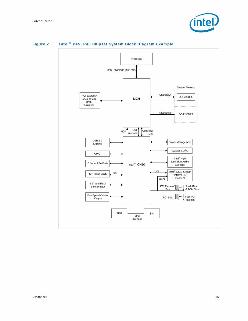
Datasheet 25
Introduction
Figure 2. Intel® P45, P43 Chipset System Block Diagram Example
Processor
MCH DDR2/DDR3
DDR2/DDR3
Channel A
800/1066/1333 MHz FSB
HDA
Channel B
PCI Express* 1x16 or 2x8
(P45) Graphics
System Memory
Intel® ICH10
USB 2.012 ports
GPIO
6 Serial ATA Ports
SPI
TPM
Intel® High Definition Audio
Codec(s)
LPC Interface
Power Management
SST and PECI Sensor Input
Fan Speed Control Output
SMBus 2.0/I2C
Intel® 82567 Gigabit Platform LAN
Connect
SIO
SPI Flash BIOSLCI
PCI Express* Bus
5 w/LANor 6 PCIe Slots
PCI Bus Four PCI Masters
GLCI
DMIInterface
Controller Link

Introduction
26 Datasheet
Figure 3. Intel® G41 Express Chipset System Block Diagram Example
Processor
GMCH DDR2/DDR3
DDR2/DDR3
Channel A
800/1066/1333 MHz FSB
Channel B
PCI Express* x16 Graphics
System Memory
ADD2 or MEC 8
4
4
DP/HDMI/DVI
16
DMIInterface
DP/HDMI/DVI
Intel PCI Express Gigabit Ethernet
Intel® ICH7 / Intel® ICH7R
USB 2.0(Supports 8 USB ports)
System Management(TCO)
IDE
GPIO
SMBus 2.0/I2C
Power Management
PCI Bus
...
Clock Generators
SLOT
SLOT
LAN Connect
AC ’97/Intel® HighDefinition Audio
Codec(s)
Firmware Hub
Other ASICs(Optional)
LPC I/F
Super I/O
SATA (4 ports)
PCI Express* x1
TPM(Optional)
SPI BIOS

Datasheet 27
Introduction
1.1 Terminology
Term Description
ADD Card
Advanced Digital Display Card. Provides digital display options for an Intel Graphics Controller that supports ADD cards (have DVOs multiplexed with AGP interface). Keyed like an AGP 4x card and plugs into an AGP connector. Will not work with an Intel Graphics Controller that implements Intel® SDVO.
ADD2 Card
Advanced Digital Display Card – 2nd Generation. Provides digital display options for an Intel graphics controller that supports ADD2 cards. Plugs into a x16 PCI Express* connector but utilizes the multiplexed SDVO interface. Will not work with an Intel Graphics Controller that supports Intel® DVO and ADD cards.
Chipset / Root – Complex
Used in this specification to refer to one or more hardware components that connect processor complexes to the I/O and memory subsystems. The chipset may include a variety of integrated devices.
CLinkController Link is a proprietary chip-to-chip connection between the (G)MCH and ICH10. The Intel 4 Series Chipset family requires that Clink be connected in the platform.
Core The internal base logic in the (G)MCH
CRT Cathode Ray Tube
DBI Dynamic Bus Inversion
DDR2 A second generation Double Data Rate SDRAM memory technology
DDR3 A third generation Double Data Rate SDRAM memory technology
DMIDirect Media Interface is a proprietary chip-to-chip connection between the (G)MCH and ICH. This interface is based on the standard PCI Express* specification.
DomainA collection of physical, logical or virtual resources that are allocated to work together. Domain is used as a generic term for virtual machines, partitions, etc.
DVIDigital Video Interface. Specification that defines the connector and interface for digital displays.
DVMT Dynamic Video Memory Technology
EP PCI Express Egress Port
FSB Front Side Bus. Synonymous with Host or processor bus
Full ResetFull reset is when PWROK is de-asserted. Warm reset is when both RSTIN# and PWROK are asserted.
GMCH
Graphics and Memory Controller Hub component that contains the processor interface, DRAM controller, and PCI Express port. The GMCH contains an integrated graphics device (IGD). The GMCH communicates with the I/O controller hub (Intel® ICH) over the DMI interconnect.
MEC
Media Expansion Card. Provides digital display options for an Intel Graphics Controller that supports MEC cards. Plugs into an x16 PCI Express connector but utilizes the multiplexed SDVO interface. Adds Video In capabilities to platform. Will not work with an Intel Graphics Controller that supports DVO and ADD cards. Will function as an ADD2 card in an ADD2 supported system, but Video In capabilities will not work.
HDMI
High Definition Multimedia Interface – HDMI supports standard, enhanced, or high-definition video, plus multi-channel digital audio on a single cable. It transmits all ATSC HDTV standards and supports 8-channel digital audio, with bandwidth to spare for future requirements and enhancements (additional details available through http://www.hdmi.org/)
Host This term is used synonymously with processor

Introduction
28 Datasheet
IGD Internal Graphics Device
INTx An interrupt request signal where X stands for interrupts A, B, C and D
Intel® ICH10Tenth generation I/O Controller Hub component that contains the primary PCI interface, LPC interface, USB2.0, SATA, and other I/O functions.
Intel® ICH7
Seventh generation I/O Controller Hub component that contains additional functionality compared to previous Intel ICH components. ICH7 contains the primary PCI interface, LPC interface, USB2, SATA, ATA-100, and other I/O functions. It communicates with the (G)MCH over a proprietary interconnect called DMI. For the 82G41 GMCH, the term Intel ICH in this document refers to the ICH7.
IOQ In Order Queue
LCD Liquid Crystal Display
LVDSLow Voltage Differential Signaling. A high speed, low power data transmission standard used for display connections to LCD panels.
MCHMemory Controller Hub component that contains the processor interface, DRAM controller, and PCI Express port. The MCH communicates with the I/O controller hub over the DMI interconnect.
MSIMessage Signaled Interrupt. A transaction conveying interrupt information to the receiving agent through the same path that normally carries read and write commands.
OOQ Out of Order Queueing
PAVPProtected Audio-Video Path for supporting secure playback of Intel HD Audio and Video content
PCI Express*A high-speed serial interface whose configuration is software compatible with the legacy PCI specifications.
Primary PCI The physical PCI bus that is driven directly by the ICH10/ICH7 component. Communication between Primary PCI and the (G)MCH occurs over DMI. The Primary PCI bus is not PCI Bus 0 from a configuration standpoint.
ProcessorRefers to the microprocessor that connects to chipset through the FSB interface on the (G)MCH.
RankA unit of DRAM corresponding to eight x8 SDRAM devices in parallel or four x16 SDRAM devices in parallel, ignoring ECC. These devices are usually, but not always, mounted on a single side of a DIMM.
SCI System Control Interrupt. Used in ACPI protocol.
SDVO
Serial Digital Video Out (SDVO). Digital display channel that serially transmits digital display data to an external SDVO device. The SDVO device accepts this serialized format and then translates the data into the appropriate display format (i.e., TMDS, LVDS, and TV-Out). This interface is not electrically compatible with the previous digital display channel - DVO. The SDVO interface is multiplexed on a portion of the x16 graphics PCI Express interface.
SDVO DeviceThird party codec that uses SDVO as an input. The device may have a variety of output formats, including DVI, LVDS, HDMI, TV-out, etc.
SERRSystem Error. An indication that an unrecoverable error has occurred on an I/O bus.
SMI
System Management Interrupt. SMI is used to indicate any of several system conditions such as thermal sensor events, throttling activated, access to System Management RAM, chassis open, or other system state related activity.
TMDSTransition Minimized Differential Signaling. Signaling interface from Silicon Image that is used in DVI and HDMI.
Term Description

Datasheet 29
Introduction
TPM Trusted Platform Module
UMAUnified Memory Architecture. Describes an IGD using system memory for its frame buffers.
VCO Voltage Controlled Oscillator
Term Description
Table 2. Intel Specification
Document Name Location
Intel® 4 Series Chipset Family Specification Updatehttp://www.intel.com/assets/pdf/specupdate/319971.pdf
Intel® 4 Series Chipset Family Thermal and Mechanical Design Guide
http://www.intel.com/assets/pdf/designguide/319972.pdf
Intel® I/O Controller Hub 10 (ICH10) Family Datasheethttp://www.intel.com/Assets/PDF/datasheet/319973.pdf
Intel® I/O Controller Hub 10 (ICH10) Family Thermal Mechanical Design Guide.
http://www.intel.com/assets/pdf/designguide/319975.pdf
Intel® I/O Controller Hub 7 (ICH7) Family Datasheethttp://www.intel.com/assets/pdf/datasheet/307013.pdf
Intel® I/O Controller Hub 7 (ICH7) Family Thermal Mechanical Design Guide.
http://www.intel.com/assets/pdf/designguide/307015.pdf
Advanced Configuration and Power Interface Specification, Version 2.0
http://www.acpi.info/
Advanced Configuration and Power Interface Specification, Version 1.0b
http://www.acpi.info/
The PCI Local Bus Specification, Version 2.3 http://www.pcisig.com/specifications
PCI Express* Specification, Version 1.1http://www.pcisig.com/specifications

Introduction
30 Datasheet
1.2 (G)MCH System Overview
The (G)MCH was designed for use with the Intel® Core™2 Extreme processor QX9000 series, Intel® Core™2 Quad processor Q9000 series, and Intel® Core™2 Duo processor E8000 and E7000 series in the LGA775 Land Grid Array Package targeted for desktop platforms. The role of a (G)MCH in a system is to manage the flow of information between its interfaces: the processor interface, the System Memory interface, the External Graphics or PCI Express interface, internal graphics interfaces, and the I/O Controller through DMI interface. This includes arbitrating between the interfaces when each initiates transactions. It supports one or two channels of DDR2 or DDR3 SDRAM. It also supports PCI Express based external graphics and devices. The Intel 4 Series Chipset platform supports the tenth generation I/O Controller Hub 10 (ICH10) to provide I/O related features. Note that the Intel G41 Chipset supports the I/O Controller Hub 7 (ICH7).
1.2.1 Host Interface
The (G)MCH supports a single LGA775 socket processor. The (G)MCH supports a FSB frequency of 800, 1066, 1333 MHz. Host-initiated I/O cycles are decoded to PCI Express, DMI, or the (G)MCH configuration space. Host-initiated memory cycles are decoded to PCI Express, DMI, or system memory. PCI Express device accesses to non-cacheable system memory are not snooped on the host bus. Memory accesses initiated from PCI Express using PCI semantics and from DMI to system SDRAM will be snooped on the host bus.
Processor/Host Interface (FSB) Details
• Supports Intel® Core™2 Extreme processor QX9000 series, Intel® Core™2 Quad processor Q9000 series, and Intel® Core™2 Duo processor E8000 and E7000 series Family processors
• Supports Front Side Bus (FSB) at the following Frequency Ranges:
— 800, 1066, 1333 MT/s. FSB speeds are processor dependent.
• Supports FSB Dynamic Bus Inversion (DBI)
• Supports 36-bit host bus addressing, allowing the processor to access the entire 64 GB of the host address space.
• Has a 12-deep In-Order Queue to support up to twelve outstanding pipelined address requests on the host bus
• Has a 1-deep Defer Queue
• Uses GTL+ bus driver with integrated GTL termination resistors
• Supports a Cache Line Size of 64 bytes

Datasheet 31
Introduction
1.2.2 System Memory Interface
The (G)MCH integrates a system memory DDR2/DDR3 controller with two, 64-bit wide interfaces. The buffers support both SSTL_1.8 (Stub Series Terminated Logic for 1.8 V) and SSTL_1.5 (Stub Series Terminated Logic for 1.5V) signal interfaces. The memory controller interface is fully configurable through a set of control registers.
System Memory Interface Details
• Directly supports one or two channels of DDR2 or DDR3 memory with a maximum of two DIMMs per channel.
• Supports single and dual channel memory organization modes.
• Supports a data burst length of eight for all memory organization modes.
• Supported memory data transfer rates:
— 667 MHz and 800 MHz for DDR2
— 800 MHz and 1066 MHz for DDR3.
• I/O Voltage of 1.8 V for DDR2 and 1.5 V for DDR3.
• Supports both un-buffered non-ECC DDR2 or non-ECC DDR3 DIMMs.
• Supports maximum memory bandwidth of 6.4 GB/s in single-channel mode or 12.8 GB/s in dual-channel mode assuming DDR2 800 MHz.
• Supports 512-Mb, 1-Gb, 2-Gb DDR2 and 512-Mb, 1-Gb DDR3 DRAM technologies for x8 and x16 devices.
• Using 512 Mb device technologies, the smallest memory capacity possible is 256 MB, assuming Single Channel Mode with a single x16 single sided un-buffered non-ECC DIMM memory configuration.
• Using 2 Gb device technologies, the largest memory capacity possible is 16 GB, assuming Dual Channel Mode with four x8 double sided un-buffered non-ECC or ECC DIMM memory configurations. NOTE: The ability to support greater than the largest memory capacity is subject to availability of higher density memory devices.
• Supports up to 32 simultaneous open pages per channel (assuming 4 ranks of 8 bank devices)
• Supports opportunistic refresh scheme
• Supports Partial Writes to memory using Data Mask (DM) signals
• Supports a memory thermal management scheme to selectively manage reads and/or writes. Memory thermal management can be triggered either by on-die thermal sensor, or by preset limits. Management limits are determined by weighted sum of various commands that are scheduled on the memory interface.
1.2.3 Direct Media Interface (DMI)
Direct Media Interface (DMI) is the chip-to-chip connection between the (G)MCH and ICH10/ICH7. This high-speed interface integrates advanced priority-based servicing allowing for concurrent traffic and true isochronous transfer capabilities. Base functionality is completely software transparent permitting current and legacy software to operate normally.
To provide for true isochronous transfers and configurable Quality of Service (QoS) transactions, the ICH10/ICH7 supports two virtual channels on DMI: VC0 and VC1. These two channels provide a fixed arbitration scheme where VC1 is always the highest

Introduction
32 Datasheet
priority. VC0 is the default conduit of traffic for DMI and is always enabled. VC1 must be specifically enabled and configured at both ends of the DMI link (i.e., the ICH10/ICH7 and (G)MCH).
• A chip-to-chip connection interface to Intel ICH10/ICH7 • 2 GB/s point-to-point DMI to ICH10 (1 GB/s each direction)• 100 MHz reference clock (shared with PCI Express)• 32-bit downstream addressing• APIC and MSI interrupt messaging support. Will send Intel-defined “End Of
Interrupt” broadcast message when initiated by the processor.• Message Signaled Interrupt (MSI) messages• SMI, SCI, and SERR error indication
1.2.4 Multiplexed PCI Express* Graphics Interface and Intel® sDVO/DVI/HDMI/DP Interface
For the 82Q45, 82Q43, 82B43, 82G45, 82G43, and 82G41 GMCHs, the PCI Express Interface is multiplexed with the SDVO and HDMI/DVI interfaces. For the 82P45 and 82P43 MCHs, the PCI Express Interface is not multiplexed.
1.2.4.1 PCI Express* Interface
The (G)MCH supports either two PCI Express* 8-lane (x8) ports or one PCI Express 16-lane (x16) port.
The (G)MCH contains one 16-lane (x16) PCI Express port intended for supporting up to two external PCI Express graphics card in bifurcated mode, fully compliant to the PCI Express Base Specification, Revision 2.0.
• Supports PCI Express GEN1 frequency of 1.25 GHz resulting in 2.5 Gb/s each direction (500 MB/s total). Maximum theoretical bandwidth on interface of 4 GB/s in each direction simultaneously, for an aggregate of 8 GB/s when operating in x16 mode.
• Supports PCI Express GEN2 frequency of 2.5 GHz resulting in 5.0 Gb/s each direction (1000 MB/s total). Maximum theoretical bandwidth on interface of 8 GB/s in each direction simultaneously, for an aggregate of 16 GB/s when operating in x16 mode.
• PCI Express port 0 is mapped to PCI Device 1 (PEG).• PCI Express port 1 is mapped to PCI Device 6 (PEG2).• Peer to Peer traffic is supported on Virtual Channel 0:
— From DMI to PEG— From DMI to PEG2— From PEG to PEG2— From PEG2 to PEG
• Supports PCI Express Enhanced Access Mechanism. Allowing accesses to the device configuration space in a flat memory mapped fashion.
• The port may negotiate down to narrower widths. For each of the ports:— Support for x16/x8/x4/x1 widths for a single PEG mode.— Support for the x8/x4/x1 widths for a dual PEG mode.— x1 width support simultaneously with the sDVO functionality which is
multiplexed onto the PEG port. Such shared use facilitates ADD2+/MEC implementation.
• The x16 lanes can be configured to two ports in bifurcated mode. In this mode, maximum x8 width is supported.

Datasheet 33
Introduction
• The two x8 PCI Express ports can operate in GEN1 or GEN2 mode independent of each other.
• Supports “static” lane numbering reversal. — Does not support “dynamic” lane reversal, as defined (optional) by the PCI
Express Specification.• Supports L1 ASPM power management capability.
1.2.4.2 sDVO Multiplexed Interface (Intel® 82Q45, 82Q43, 82B43, 82G45, 82G43, 82G41 GMCH Only)
The GMCH supports two multiplexed SDVO ports that each drive pixel clocks up to 270 MHz. The GMCH can make use of these digital display channels via an Advanced Digital Display card (ADD2) or Media Expansion card.
1.2.4.3 HDMI/DVI/DP Multiplexed Interface (Intel® 82Q45, 82Q43, 82B43, 82G45, 82G43, 82G41 GMCH Only)
The GMCH supports two multiplexed digital display ports that each drive pixel clocks up to 165 MHz. The GMCH Supports combinations of DP/DP, DVI/DVI, HDMI/HDMI*, DP/DVI, HDMI/DVI, and DP/HDMI multiplexed on the 2 digital display ports.
Note: Only one channel can support embedded audio at a time.
1.2.5 Graphics Features (Intel® 82Q45, 82Q43, 82B43, 82G45, 82G43, 82G41 GMCH Only)
The GMCH provides an integrated graphics device (IGD) delivering cost competitive 3D, 2D and video capabilities. DX10 and OpenGL 2.1 are supported. The GMCH contains an extensive set of instructions for 3D operations, 2D operations, motion compensation, overlay, and display control. HD-DVD and Blu-Ray are also natively supported with hardware based VC-1, MPEG2, and AVC decode capabilities. The GMCH also supports PAVP (Protected Audio-Video Path), which allows for protected Intel® HD Audio HD Video Playback.
The GMCH uses a UMA configuration with DVMT for graphics memory. The GMCH also has the capability to support external graphics accelerators via the PCI Express Graphics (PEG) port but cannot work concurrently with the integrated graphics device. High bandwidth access to data is provided through the system memory port.
1.2.6 (G)MCH Clocking
• Differential host clock of 200/266/333 MHz. The (G)MCH supports FSB transfer rates of 800/1066/1333 MT/s.
• Differential memory clocks of 333/400/533/600 MHz. The (G)MCH supports memory transfer rates of DDR2-667, DDR2-800, DDR3-800, and DDR3-1067.
• The PCI Express* PLL of 100 MHz Serial Reference Clock generates the PCI Express core clock of 250 MHz.
• Display timings are generated from display PLLs that use a 96 MHz differential non-spread spectrum clock as a reference. Display PLLs can also use the sSDVO_TVCLKIN[+/-] from an SDVO device as a reference. (82Q45, 82Q43, 82B43, 82G45, 82G43, and 82G41 GMCH only)
• All of the above clocks are capable of tolerating Spread Spectrum clocking.
• Host, memory, and PCI Express PLLs are disabled until PWROK is asserted.

Introduction
34 Datasheet
1.2.7 Power Management
(G)MCH Power Management support includes:
• PC99 suspend to DRAM support (“STR”, mapped to ACPI state S3)
• SMRAM space remapping to A0000h (128 KB)
• Supports extended SMRAM space above 256 MB, additional 1 MB TSEG from the Base of graphics stolen memory (BSM) when enabled, and cacheable (cacheability controlled by processor)
• ACPI Rev 3.0b compatible power management
• Supports Active State Power Management (ASPM)
• Supports processor states: C0, C1, C2, C3, and C4
• Supports System states: S0, S1, S3, and S5
• Supports processor Thermal Management 2 (TM2)
• Supports Manageability states M0, M1–S3, M1–S5, Moff–S3, Moff–S5, Moff-M1
1.2.8 Thermal Sensor
(G)MCH Thermal Sensor support includes:
• Catastrophic Trip Point support for emergency clock gating for the (G)MCH
• Hot Trip Point support for SMI generation
§ §

Datasheet 35
Signal Description
2 Signal Description
This chapter provides a detailed description of (G)MCH signals. The signals are arranged in functional groups according to their associated interface.
The following notations are used to describe the signal type.
Signal Type Description
PCI Express*
PCI Express interface signals. These signals are compatible with PCI Express 2.0 Signaling Environment AC Specifications and are AC coupled. The buffers are not 3.3 V tolerant. Differential voltage spec = (|D+ – D-|) * 2 = 1.2 Vmax. Single-ended maximum = 1.25 V. Single-ended minimum = 0 V.
DMI
Direct Media Interface signals. These signals are compatible with PCI Express 2.0 Signaling Environment AC Specifications, but are DC coupled. The buffers are not 3.3 V tolerant. Differential voltage spec = (|D+ – D-|) * 2 = 1.2 Vmax. Single-ended maximum = 1.25 V. Single-ended minimum = 0 V.
CMOS CMOS buffers. 1.5 V tolerant.
COD CMOS Open Drain buffers. 3.3 V tolerant.
HVCMOS High Voltage CMOS buffers. 3.3 V tolerant.
HVIN High Voltage CMOS input-only buffers. 3.3 V tolerant.
SSTL_1.8Stub Series Termination Logic. These are 1.8 V output capable buffers. 1.8 V tolerant.
SSTL_1.5Stub Series Termination Logic. These are 1.5 V output capable buffers. 1.5 V tolerant
AAnalog reference or output. May be used as a threshold voltage or for buffer compensation.
GTL+Gunning Transceiver Logic signaling technology. Implements a voltage level as defined by VTT of 1.2 V and/or 1.1 V.

Signal Description
36 Datasheet
2.1 Host Interface Signals
Note: Unless otherwise noted, the voltage level for all signals in this interface is tied to the termination voltage of the Host Bus (VTT).
Signal Name Type Description
FSB_ADSBI/O
GTL+
Address Strobe: The processor bus owner asserts FSB_ADSB to indicate the first of two cycles of a request phase. The (G)MCH can assert this signal for snoop cycles and interrupt messages.
FSB_BNRBI/O
GTL+
Block Next Request: Used to block the current request bus owner from issuing new requests. This signal is used to dynamically control the processor bus pipeline depth.
FSB_BPRIBO
GTL+
Priority Agent Bus Request: The (G)MCH is the only Priority Agent on the processor bus. It asserts this signal to obtain the ownership of the address bus. This signal has priority over symmetric bus requests and will cause the current symmetric owner to stop issuing new transactions unless the FSB_LOCKB signal was asserted.
FSB_BREQ0BO
GTL+
Bus Request 0: The (G)MCH pulls the processor bus’ FSB_BREQ0B signal low during FSB_CPURSTB. The processors sample this signal on the active-to-inactive transition of FSB_CPURSTB. The minimum setup time for this signal is 4 HCLKs. The minimum hold time is 2 HCLKs and the maximum hold time is 20 HCLKs. FSB_BREQ0B should be tri-stated after the hold time requirement has been satisfied.
FSB_CPURSTBO
GTL+
CPU Reset: The FSB_CPURSTB pin is an output from the (G)MCH. The (G)MCH asserts FSB_CPURSTB while RSTINB (PCIRST# from the ICH) is asserted and for approximately 1 ms after RSTINB is de-asserted. The FSB_CPURSTB allows the processor to begin execution in a known state.
FSB_DBSYBI/O
GTL+Data Bus Busy: Used by the data bus owner to hold the data bus for transfers requiring more than one cycle.
FSB_DEFERBO
GTL+
Defer: Signals that the (G)MCH will terminate the transaction currently being snooped with either a deferred response or with a retry response.
FSB_DINVB_[3:0]I/O
GTL+ 4x
Dynamic Bus Inversion: Driven along with the FSB_DB_[63:0] signals. Indicates if the associated signals are inverted or not. FSB_DINVB_[3:0] are asserted such that the number of data bits driven electrically low (low voltage) within the corresponding 16 bit group never exceeds 8.FSB_DINVB_x Data BitsFSB_DINVB_3 FSB_DB_[63:48]FSB_DINVB_2 FSB_DB_[47:32]FSB_DINVB_1 FSB_DB_[31:16]FSB_DINVB_0 FSB_DB_[15:0]
FSB_DRDYBI/O
GTL+Data Ready: Asserted for each cycle that data is transferred.

Datasheet 37
Signal Description
FSB_AB_[35:3]I/O
GTL+ 2x
Host Address Bus: FSB_AB_[35:3] connect to the processor address bus. During processor cycles the FSB_AB_[35:3] are inputs. The (G)MCH drives FSB_AB_[35:3] during snoop cycles on behalf of DMI and PCI Express initiators. FSB_AB_[35:3] are transferred at 2x rate. Note that the address is inverted on the processor bus. The values are driven by the (G)MCH between PWROK assertion and FSB_CPURSTINB deassertion to allow processor configuration.
FSB_ADSTBB_[1:0]I/O
GTL+ 2x
Host Address Strobe: The source synchronous strobes used to transfer FSB_AB_[31:3] and FSB_REQB_[4:0] at the 2x transfer rate.Strobe Address BitsFSB_ADSTBB_0 FSB_AB_[16:3], FSB_REQB_[4:0]FSB_ADSTBB_1 FSB_AB_[31:17]
FSB_DB_[63:0]I/O
GTL+ 4x
Host Data: These signals are connected to the processor data bus. Data on FSB_DB_[63:0] is transferred at a 4x rate. Note that the data signals may be inverted on the processor bus, depending on the FSB_DINVB_[3:0] signals.
FSB_DSTBPB_[3:0]FSB_DSTBNB_[3:0]
I/OGTL+ 4x
Differential Host Data Strobes: The differential source synchronous strobes used to transfer FSB_DB_[63:0] and FSB_DINVB_[3:0] at the 4x transfer rate.Named this way because they are not level sensitive. Data is captured on the falling edge of both strobes. Hence, they are pseudo-differential, and not true differential.Strobe Data BitsFSB_DSTB[P,N]B_3 FSB_DB_[63:48], HDINVB_3FSB_DSTB[P,N]B_2 FSB_DB_[47:32], HDINVB_2FSB_DSTB[P,N]B_1 FSB_DB_[31:16], HDINVB_1FSB_DSTB[P,N]B_0 FSB_DB_[15:0], HDINVB_0
FSB_HITBI/O
GTL+
Hit: Indicates that a caching agent holds an unmodified version of the requested line. Also, driven in conjunction with FSB_HITMB by the target to extend the snoop window.
FSB_HITMBI/O
GTL+
Hit Modified: Indicates that a caching agent holds a modified version of the requested line and that this agent assumes responsibility for providing the line. Also, driven in conjunction with FSB_HITB to extend the snoop window.
FSB_LOCKBI
GTL+
Host Lock: All processor bus cycles sampled with the assertion of FSB_LOCKB and FSB_ADSB, until the negation of FSB_LOCKB must be atomic, i.e. no DMI or PCI Express access to DRAM are allowed when FSB_LOCKB is asserted by the processor.
FSB_REQB_[4:0]I/O
GTL+2x
Host Request Command: Defines the attributes of the request. FSB_REQB_[4:0] are transferred at 2x rate. Asserted by the requesting agent during both halves of Request Phase. In the first half the signals define the transaction type to a level of detail that is sufficient to begin a snoop request. In the second half the signals carry additional information to define the complete transaction type.The transactions supported by the (G)MCH Host Bridge are defined in the Host Interface section of this document.
Signal Name Type Description

Signal Description
38 Datasheet
FSB_TRDYBO
GTL+Host Target Ready: Indicates that the target of the processor transaction is able to enter the data transfer phase.
FSB_RSB_[2:0]O
GTL+
Response Signals: Indicates type of response according to the table at left:Encoding Response Type000 Idle state001 Retry response010 Deferred response011 Reserved (not driven by (G)MCH)100 Hard Failure (not driven by (G)MCH)101 No data response110 Implicit Writeback111 Normal data response
FSB_RCOMPI/OA
Host RCOMP: Used to calibrate the Host GTL+ I/O buffers. This signal is powered by the Host Interface termination rail (VTT). Connects to FSB_XRCOMP1IN in the package.
FSB_SCOMPI/OA
Slew Rate Compensation: Compensation for the Host Interface for rising edges.
FSB_SCOMPBI/OA
Slew Rate Compensation: Compensation for the Host Interface for falling edges.
FSB_SWINGI/OA
Host Voltage Swing: These signals provide reference voltages used by the FSB RCOMP circuits. FSB_XSWING is used for the signals handled by FSB_XRCOMP.
FSB_DVREFI/OA
Host Reference Voltage: Reference voltage input for the Data signals of the Host GTL interface.
FSB_ACCVREFI/OA
Host Reference Voltage: Reference voltage input for the Address signals of the Host GTL interface.
Signal Name Type Description

Datasheet 39
Signal Description
2.2 System Memory (DDR2/DDR3) Interface Signals
2.2.1 System Memory Channel A Interface Signals
Signal Name Type Description
DDR_A_CKO
SSTL-1.8/1.5
SDRAM Differential Clocks:• DDR2: Three per DIMM• DDR3: Two per DIMM
DDR_A_CKBO
SSTL-1.8/1.5
SDRAM Inverted Differential Clocks:• DDR2: Three per DIMM• DDR3: Two per DIMM
DDR_A_CSB_[3:0]O
SSTL-1.8/1.5DDR2/DDR3 Device Rank 3, 2, and 0 Chip Selects
DDR_A_CKE_[3:0]O
SSTL-1.8/1.5DDR2/DDR3 Clock Enable:(1 per Device Rank)
DDR_A_ODT_[3:0]O
SSTL-1.8/1.5DDR2/DDR3 On Die Termination:(1 per Device Rank)
DDR_A_MA_[14:0]O
SSTL-1.8/1.5DDR2 Address Signals [14:0]
DDR_A_BS_[2:0]O
SSTL-1.8/1.5DDR2/DDR3 Bank Select
DDR_A_RASBO
SSTL-1.8/1.5DDR2/DDR3 Row Address Select signal
DDR_A_CASBO
SSTL-1.8/1.5DDR2/DDR3 Column Address Select signal
DDR_A_WEBO
SSTL-1.8/1.5DDR2/DDR3 Write Enable signal
DDR_A_DQ_[63:0]I/O
SSTL-1.8/1.5DDR2/DDR3 Data Lines
DDR_A_DM_[7:0]O
SSTL-1.8/1.5DDR2/DDR3 Data Mask
DDR_A_DQS_[7:0]I/O
SSTL-1.8/1.5DDR2/DDR3 Data Strobes
DDR_A_DQSB_[7:0]I/O
SSTL-1.8/1.5DDR2/DDR3 Data Strobe Complements

Signal Description
40 Datasheet
2.2.2 System Memory Channel B Interface Signals
Signal Name Type Description
DDR_B_CKO
SSTL-1.8/1.5
SDRAM Differential Clocks:• DDR2: Three per DIMM• DDR3: Two per DIMM
DDR_B_CKBO
SSTL-1.8/1.5
SDRAM Inverted Differential Clocks:• DDR2: Three per DIMM• DDR3: Two per DIMM
DDR_B_CSB_[3:0]O
SSTL-1.8/1.5DDR2/DDR3 Device Rank 3, 2, 1, and 0 Chip Select
DDR_B_CKE_[3:0]O
SSTL-1.8/1.5DDR2/DDR3 Clock Enable:(1 per Device Rank)
DDR_B_ODT_[3:0]O
SSTL-1.8/1.5DDR2/DDR3 Device Rank 3, 2, 1, and 0 On Die Termination
DDR_B_MA_[14:0]O
SSTL-1.8/1.5DDR2/DDR3 Address Signals [14:0]
DDR_B_BS_[2:0]O
SSTL-1.8/1.5DDR2/DDR3 Bank Select
DDR_B_RASBO
SSTL-1.8/1.5DDR2/DDR3 Row Address Select signal
DDR_B_CASBO
SSTL-1.8/1.5DDR2/DDR3 Column Address Select signal
DDR_B_WEBO
SSTL-1.8/1.5DDR2/DDR3 Write Enable signal
DDR_B_DQ_[63:0]I/O
SSTL-1.8/1.5DDR2/DDR3 Data Lines
DDR_B_DM_[7:0]O
SSTL-1.8/1.5DDR2/DDR3 Data Mask
DDR_B_DQS_[7:0]I/O
SSTL-1.8/1.5DDR2/DDR3 Data Strobes
DDR_B_DQSB_[7:0]I/O
SSTL-1.8/1.5DDR2/DDR3 Data Strobe Complements

Datasheet 41
Signal Description
2.2.3 System Memory Miscellaneous Signals
2.3 PCI Express* Interface Signals
Signal Name Type Description
DDR_RPDI/OA
System Memory Pull-down RCOMP
DDR_RPUI/OA
System Memory Pull-up RCOMP
DDR_SPDI/OA
System Memory Pull-down RCOMP
DDR_SPUI/OA
System Memory Pull-up RCOMP
DDR_VREFIA
System Memory Reference Voltage
DDR3_DRAM_PWROKIA
DDR3 VCC_DDR Power OK
DDR3_DRAMRSTBO
SSTL-1.5DDR3 Reset Signal
DDR3_A_CSB1O
SSTL-1.8/1.5DDR3 CSB1 Signal
DDR3_A_MA0O
SSTL-1.8/1.5DDR3 MA0 Signal
DDR3_A_WEBO
SSTL-1.8/1.5DDR3 WEB Signal
DDR3_B_ODT3O
SSTL-1.8/1.5DDR3 ODT3 Signal
Signal Name Type Description
PEG_RXN_[15:0]PEG_RXP_[15:0]
I/OPCIE
Primary PCI Express Receive Differential Pair
PEG_TXN_[15:0]PEG_TXP_[15:0]
OPCIE
Primary PCI Express Transmit Differential Pair
EXP_ICOMPOIA
Primary PCI Express Output Current Compensation
EXP_COMPIIA
Primary PCI Express Input Current Compensation
EXP_RCOMPOIA
Primary PCI Express Resistive Compensation
EXP_RBIASIA
Primary PCI Express Bias

Signal Description
42 Datasheet
2.4 Controller Link Interface Signals
2.5 Analog Display Signals (Intel® 82Q45, 82Q43, 82B43, 82G45, 82G43, 82G41 GMCH Only)
Signal Name Type Description
CL_DATAI/O
CMOSController Link Data (Bi-directional)
CL_CLKI/O
CMOSController Link Clock (Bi-directional)
CL_VREFI
CMOSController Link VREF
CL_RST#I
CMOSController Link Reset (Active low)
Signal Name Type Description
CRT_REDOA
RED Analog Video Output: This signal is a CRT Analog video output from the internal color palette DAC. The DAC is designed for a 37.5 ohm routing impedance but the terminating resistor to ground will be 75 ohms. (e.g., 75 ohm resistor on the board, in parallel with a 75 ohm CRT load).
CRT_GREENOA
GREEN Analog Video Output: This signal is a CRT Analog video output from the internal color palette DAC. The DAC is designed for a 37.5 ohm routing impedance but the terminating resistor to ground will be 75 ohms. (e.g., 75 ohm resistor on the board, in parallel with a 75 ohm CRT load).
CRT_BLUEOA
BLUE Analog Video Output: This signal is a CRT Analog video output from the internal color palette DAC. The DAC is designed for a 37.5 ohm routing impedance but the terminating resistor to ground will be 75 ohms. (e.g., 75 ohm resistor on the board, in parallel with a 75 ohm CRT load).
CRT_IREFI/OA
Resistor Set: Set point resistor for the internal color palette DAC. A 255 ohm 1% resistor is required between CRT_IREF and motherboard ground.
CRT_HSYNCO
HVCMOS
CRT Horizontal Synchronization: This signal is used as the horizontal sync (polarity is programmable) or “sync interval”. 2.5 V output.
CRT_VSYNCO
HVCMOSCRT Vertical Synchronization: This signal is used as the vertical sync (polarity is programmable). 2.5 V output.
CRT_DDC_CLKI/OCOD
Monitor Control Clock
CRT_DDC_DATAI/OCOD
Monitor Control Data
CRT_IRTNI/OCOD
Monitor Interrupt Return

Datasheet 43
Signal Description
2.6 Clocks, Reset, and Miscellaneous
Signal Name Type Description
HPL_CLKINPHPL_CLKINN
ICMOS
Differential Host Clock In: These pins receive a differential host clock from the external clock synthesizer. This clock is used by all of the (G)MCH logic that is in the Host clock domain.
EXP_CLKPEXP_CLKN
ICMOS
Differential Primary PCI Express Clock In: These pins receive a differential 100 MHz Serial Reference clock from the external clock synthesizer. This clock is used to generate the clocks necessary for the support of Primary PCI Express and DMI.
DPL_REFCLKINNDPL_REFCLKINP
ICMOS
Display PLL Differential Clock In: Tie DPL_REFCLKINP to VCC and tie DPL_REFCLKINN to ground when not using DP.
DPL_REFSSCLKINPDPL_REFSSCLKINN
ICMOS
Display PLL Differential Clock In: Tie DPL_REFSSCLKINP to VCC and tie DPL_REFSSCLKINN to ground when not using DP.
RSTINBI
SSTL
Reset In: When asserted, this signal will asynchronously reset the (G)MCH logic. This signal is connected to the PCIRST# output of the ICH. All PCI Express output signals and DMI output signals will also tri-state compliant to PCI Express Specification, Revision 2.0. This input should have a Schmitt trigger to avoid spurious resets.This signal is required to be 3.3 V tolerant.
CL_PWROKI/O
SSTL
CL Power OK: When asserted, CL_PWROK is an indication to the (G)MCH that core power (VCC_CL) has been stable for at least 10 us.
EXP_SLRI
CMOS
PCI Express* Static Lane Reversal/Form Factor Selection: (G)MCH’s PCI Express lane numbers are reversed to differentiate Balanced Technology Extended (BTX) and ATX form factors.0 = (G)MCH PCI Express lane numbers are reversed (BTX)1 = Normal operation (ATX)
BSEL[2:0]I
CMOS
Bus Speed Select: At the de-assertion of PWROK, the value sampled on these pins determines the expected frequency of the bus.
EXP_SMI
GTL+
Concurrent PCI Express Port Enable: Concurrent SDVO and PCI Express0 = Only SDVO or PCI Express is operational.1 = Both SDVO and PCI Express are operating simultaneously
via the PCI Express port.
NOTE: For the 82P45 and 82P42 MCH, this signal should be pulled low.
PWROKI/O
SSTLPower OK: When asserted, PWROK is an indication to the (G)MCH that core power has been stable for at least 10 us.
DPRSTPBO
HVCMOSAdvanced Power Management Signal

Signal Description
44 Datasheet
2.7 Direct Media Interface
SLPBO
HVCMOSAdvanced Power Management Signal
ICH_SYNCBO
HVCMOSICH Sync Signal
ALLZTESTI
GTL+
All Z Test: This signal is used for Chipset Bed of Nails testing to execute All Z Test. It is used as output for XOR Chain testing.
XORTESTI
GTL+XOR Chain Test: This signal is used for Chipset Bed of Nails testing to execute XOR Chain Test.
CENI
GTL+
TLS Confidentiality Enable:0 = Disable TLS1 = Enable TLS
ITPM_ENBI
GTL+
Integrated TPM Enable: 0 = Enable Intel TPM1 = Disable Intel TPM
NOTE: This signal is not used on the 82G45, 82G43, 82G41 GMCH and 82P45, 82P43 MCH.
DualX8_EnableI
GTL+
2x8 PEG Port Bifurcation:0 = 2x8 PCI Express Ports Enabled1 = 1x16 PCI Express Port Enabled
BSCANTESTI
GTL+Boundary Scan Test Enable: This signal is used to enter Boundary Scan mode
JTAG_TCKI/O
SSTLJTAG Clock
JTAG_TDII/O
SSTLJTAG Data In
JTAG_TDOI/O
SSTLJTAG Data Out
JTAG_TMSI/O
SSTLJTAG Test Mode Select
Signal Name Type Description
Signal Name Type Description
DMI_RXP_[3:0]DMI_RXN_[3:0]
IDMI
Direct Media Interface: Receive differential pair (RX). (G)MCH-ICH serial interface input.
DMI_TXP_[3:0]DMI_TXN_[3:0]
ODMI
Direct Media Interface: Transmit differential pair (TX). (G)MCH-ICH serial interface output.

Datasheet 45
Signal Description
2.8 Serial DVO Interface (Intel® 82Q45, 82Q43, 82B43, 82G45, 82G43, 82G41 GMCH Only)
Most of these signals are multiplexed with PCI Express signals. SDVO_CTTCLK and SDVO_CTRLDATA are the only unmultiplexed signals on the SDVO interface. SDVO is mapped to lanes 0–7 or lanes 15–8 of the PEG port depending on the PCI Express Static Lane Reversal and SDVO/PCI Express Coexistence straps. The lower 8 lanes are used when both straps are either asserted or not asserted. Otherwise, the upper 8 lanes are used.
Signal Name Type Description
SDVOB_CLK-O
PCIESerial Digital Video Channel B Clock Complement
SDVOB_CLK+O
PCIESerial Digital Video Channel B Clock
SDVOB_RED-O
PCIESerial Digital Video Channel C Red Complement
SDVOB_RED+O
PCIESerial Digital Video Channel C Red
SDVOB_GREEN-O
PCIESerial Digital Video Channel B Green Complement
SDVOBGREEN+O
PCIESerial Digital Video Channel B Green
SDVOB_BLUE-O
PCIESerial Digital Video Channel B Blue Complement
SDVOB_BLUE+O
PCIESerial Digital Video Channel B Blue
SDVOC_RED-O
PCIESerial Digital Video Channel C Red Complement
SDVOC_RED+O
PCIESerial Digital Video Channel C Red Channel B Alpha
SDVOC_GREEN-O
PCIESerial Digital Video Channel C Green Complement
SDVOC_GREEN+O
PCIESerial Digital Video Channel C Green
SDVOC_BLUE-O
PCIESerial Digital Video Channel C Blue Complement
SDVOC_BLUE+O
PCIESerial Digital Video Channel C Blue
SDVOC_CLK-O
PCIESerial Digital Video Channel C Clock Complement
SDVOC_CLK+O
PCIESerial Digital Video Channel C Clock

Signal Description
46 Datasheet
SDVO_TVCLKIN-I
PCIESerial Digital Video TVOUT Synchronization Clock Complement
SDVO_TVCLKINI
PCIESerial Digital Video TVOUT Synchronization Clock
SDVOB_INT-I
PCIESerial Digital Video Input Interrupt Complement
SDVOB_INT+I
PCIESerial Digital Video Input Interrupt
SDVOC_INT-I
PCIESerial Digital Video Input Interrupt Complement
SDVOC_INT+I
PCIESerial Digital Video Input Interrupt
SDVO_STALL-I
PCIESerial Digital Video Field Stall Complement
SDVO_STALL+I
PCIESerial Digital Video Field Stall
SDVO_CTRLCLKI/OCOD
Serial Digital Video Device Control Clock
SDVO_CTRLDATAI/OCOD
Serial Digital Video Device Control Data
Signal Name Type Description
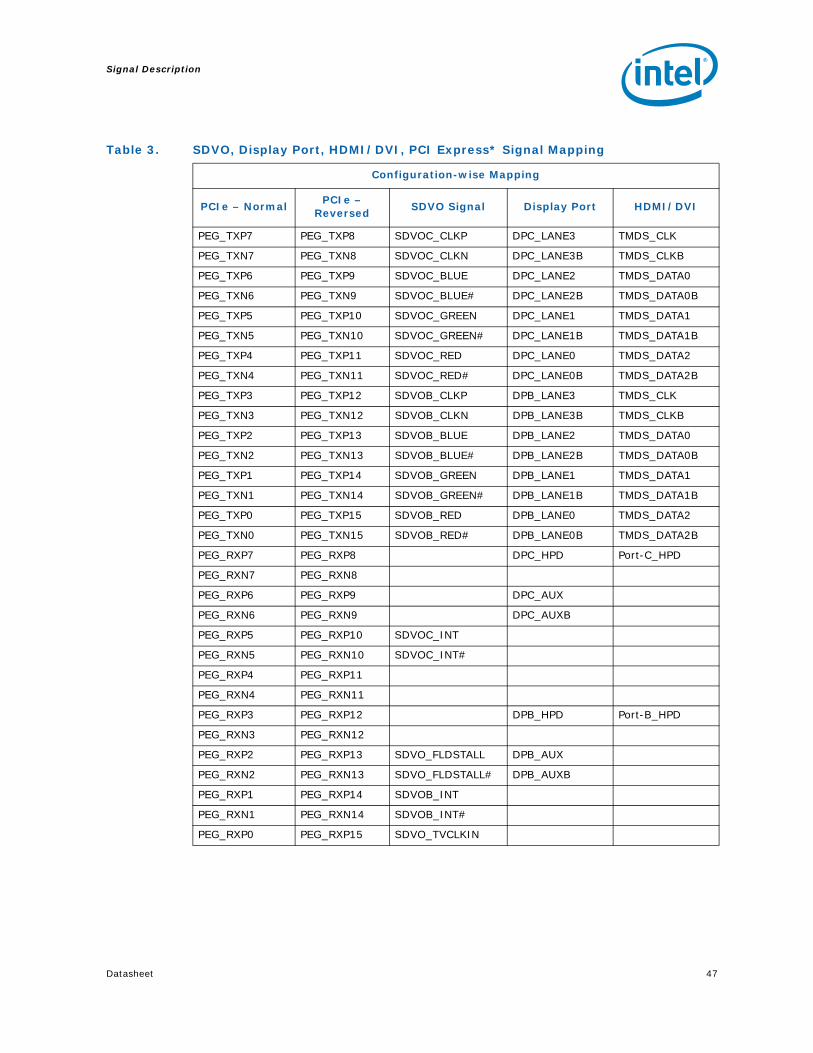
Datasheet 47
Signal Description
Table 3. SDVO, Display Port, HDMI/DVI, PCI Express* Signal Mapping
Configuration-wise Mapping
PCIe – NormalPCIe –
ReversedSDVO Signal Display Port HDMI/DVI
PEG_TXP7 PEG_TXP8 SDVOC_CLKP DPC_LANE3 TMDS_CLK
PEG_TXN7 PEG_TXN8 SDVOC_CLKN DPC_LANE3B TMDS_CLKB
PEG_TXP6 PEG_TXP9 SDVOC_BLUE DPC_LANE2 TMDS_DATA0
PEG_TXN6 PEG_TXN9 SDVOC_BLUE# DPC_LANE2B TMDS_DATA0B
PEG_TXP5 PEG_TXP10 SDVOC_GREEN DPC_LANE1 TMDS_DATA1
PEG_TXN5 PEG_TXN10 SDVOC_GREEN# DPC_LANE1B TMDS_DATA1B
PEG_TXP4 PEG_TXP11 SDVOC_RED DPC_LANE0 TMDS_DATA2
PEG_TXN4 PEG_TXN11 SDVOC_RED# DPC_LANE0B TMDS_DATA2B
PEG_TXP3 PEG_TXP12 SDVOB_CLKP DPB_LANE3 TMDS_CLK
PEG_TXN3 PEG_TXN12 SDVOB_CLKN DPB_LANE3B TMDS_CLKB
PEG_TXP2 PEG_TXP13 SDVOB_BLUE DPB_LANE2 TMDS_DATA0
PEG_TXN2 PEG_TXN13 SDVOB_BLUE# DPB_LANE2B TMDS_DATA0B
PEG_TXP1 PEG_TXP14 SDVOB_GREEN DPB_LANE1 TMDS_DATA1
PEG_TXN1 PEG_TXN14 SDVOB_GREEN# DPB_LANE1B TMDS_DATA1B
PEG_TXP0 PEG_TXP15 SDVOB_RED DPB_LANE0 TMDS_DATA2
PEG_TXN0 PEG_TXN15 SDVOB_RED# DPB_LANE0B TMDS_DATA2B
PEG_RXP7 PEG_RXP8 DPC_HPD Port-C_HPD
PEG_RXN7 PEG_RXN8
PEG_RXP6 PEG_RXP9 DPC_AUX
PEG_RXN6 PEG_RXN9 DPC_AUXB
PEG_RXP5 PEG_RXP10 SDVOC_INT
PEG_RXN5 PEG_RXN10 SDVOC_INT#
PEG_RXP4 PEG_RXP11
PEG_RXN4 PEG_RXN11
PEG_RXP3 PEG_RXP12 DPB_HPD Port-B_HPD
PEG_RXN3 PEG_RXN12
PEG_RXP2 PEG_RXP13 SDVO_FLDSTALL DPB_AUX
PEG_RXN2 PEG_RXN13 SDVO_FLDSTALL# DPB_AUXB
PEG_RXP1 PEG_RXP14 SDVOB_INT
PEG_RXN1 PEG_RXN14 SDVOB_INT#
PEG_RXP0 PEG_RXP15 SDVO_TVCLKIN

Signal Description
48 Datasheet
2.9 HDMI Interface (Intel® 82G45, 82G43, 82G41, 82B43 GMCH Only)
Signal Name Type Description
HDMIB_CLK-O
PCIESerial Digital Video Channel B Clock Complement: Multiplexed with EXP_TXN_3/EXP_TXN_12.
HDMIB_CLK+O
PCIESerial Digital Video Channel B Clock: Multiplexed with EXP_TXP_3/EXP_ TXP_12.
HDMIB_RED-O
PCIESerial Digital Video Channel B Red Complement: Multiplexed with / EXP_TXN_0./EXP_TXN_15
HDMIB_RED+O
PCIESerial Digital Video Channel B Red: Multiplexed with EXP_TXP_0/EXP__TXP_15.
HDMIB_GREEN-O
PCIESerial Digital Video Channel B Green Complement: Multiplexed with EXP_TXN_1/EXP_TXN_14.
HDMIBGREEN+O
PCIESerial Digital Video Channel B Green: Multiplexed with EXP_TXP_1/EXP_TXP_14.
HDMIB_BLUE-O
PCIESerial Digital Video Channel B Blue Complement. Multiplexed with EXP_TXN_2/EXP_TXN_13.
HDMIB_BLUE+O
PCIESerial Digital Video Channel B Blue: Multiplexed with EXP_TXP_2/EXP_TXP_13.
HDMIC_RED-O
PCIESerial Digital Video Channel C Red Complement: Multiplexed with EXP_TXN_4/EXP_TXN_11.
HDMIC_RED+O
PCIESerial Digital Video Channel C Red: Multiplexed with EXP_TXP_4/EXP_TXP_11.
HDMIC_GREEN-O
PCIESerial Digital Video Channel C Green Complement: Multiplexed with EXP_TXN_5/EXP_TXN_10.
HDMIC_GREEN+O
PCIESerial Digital Video Channel C Green: Multiplexed with EXP_TXP_5/EXP_TXP_10.
HDMIC_BLUE-O
PCIESerial Digital Video Channel C Blue Complement: Multiplexed with EXP_TXN_6/EXP_TXN_9.
HDMIC_BLUE+O
PCIESerial Digital Video Channel C Blue: Multiplexed with EXP_TXP_6/EXP_TXP_9.
HDMIC_CLK-O
PCIESerial Digital Video Channel C Clock Complement: Multiplexed with EXP_TXN_7/EXP_TXN_8.
HDMIC_CLK+O
PCIESerial Digital Video Channel C Clock: Multiplexed with EXP_TXN_7/EXP_TXP_8.
HDMI_TVCLKIN-I
PCIESerial Digital Video TVOUT Synchronization Clock Complement: Multiplexed with EXP_RXN_0/EXP_RXN_15
HDMI_TVCLKINI
PCIESerial Digital Video TVOUT Synchronization Clock: Multiplexed with EXP_RXP_0/EXP_RXP_15.
HDMIB_INT-I
PCIESerial Digital Video Input Interrupt Complement: Multiplexed with EXP_RXN_3/EXP_RXN_12.

Datasheet 49
Signal Description
Note: HDMI support on 82B43 is enabled via Intel® Upgrade Service
2.10 Display Port Interface (Intel® 82Q45, 82Q43, 82B43, 82G45, 82G43, 82G41 GMCH Only)
HDMIB_INT+I
PCIESerial Digital Video Input Interrupt: Multiplexed with EXP_RXP_3/EXP_RXP_12
HDMIC_INT-I
CIESerial Digital Video Input Interrupt: Multiplexed with EXP_RXN_7/EXP_RXN_8.
HDMIC_INT+I
PCIESerial Digital Video Input Interrupt: Multiplexed with EXP_RXP_7/EXP_RXP_8.
SDVO_CTRLCLKI/OCOD
HDMI port B Control Clock: (This pin is shared with SDVO)
SDVO_CTRLDATAI/OCOD
HDMI port B Control Data: (This pin is shared with SDVO)
DDPC_CTRLCLKI/OCOD
HDMI port C Control Clock: Also used as the DP CTRLCLK
DDPC_CTRLDATAI/OCOD
HDMI port C Control Data: Also used as the DP CTRLDATA
Signal Name Type Description
DPB_AUX#O
PCIEDisplay Port BAux channel: Multiplexed with EXP_RXN_02
DPB_AUXO
PCIEDisplay Port BAux channel: Multiplexed with EXP_RXP_02
DPB_HDPO
PCIEDisplay Port B Hot Plug Detect: Multiplexed with EXP_RXP_03
DPC_AUX#O
PCIEDisplay Port C Aux channel: Multiplexed with EXP_RXN_06
DPC_AUXO
PCIEDisplay Port C Aux channel: Multiplexed with EXP_RXP_06
DPC_HDPO
PCIEDisplay Port C Hot Plug Detect: Multiplexed with EXP_RXP_07
DPB_LANE0#O
PCIEDisplay Port B Data Lane: Multiplexed with EXP_TXN_00
DPB_LANE0O
PCIEDisplay Port B Data Lane: Multiplexed with EXP_TXP_00
DPB_LANE1#O
PCIEDisplay Port B Data Lane: Multiplexed with EXP_TXN_01
DPB_LANE1O
PCIEDisplay Port B Data Lane: Multiplexed with EXP_TXP_01
Signal Name Type Description

Signal Description
50 Datasheet
2.11 Intel® High Definition Audio Intel® 82Q45, 82Q43, 82B43,82G45, 82G43, 82G41 GMCH Only)
DPB_LANE2#O
PCIEDisplay Port B Data Lane: Multiplexed with EXP_TXN_02
DPB_LANE2O
PCIEDisplay Port B Data Lane: Multiplexed with EXP_TXP_02
DPB_LANE3#O
PCIEDisplay Port B Data Lane: Multiplexed with EXP_TXN_03
DPB_LANE3O
PCIEDisplay Port B Data Lane: Multiplexed with EXP_TXP_03
DPC_LANE0#O
PCIEDisplay Port C Data Lane: Multiplexed with EXP_TXN_04
DPC_LANE0O
PCIEDisplay Port C Data Lane: Multiplexed with EXP_TXP_04
DPC_LANE1#O
PCIEDisplay Port C Data Lane: Multiplexed with EXP_TXN_05
DPC_LANE1O
PCIEDisplay Port C Data Lane: Multiplexed with EXP_TXP_05
DPC_LANE2#O
PCIEDisplay Port C Data Lane: Multiplexed with EXP_TXN_06
DPC_LANE2O
PCIEDisplay Port C Data Lane: Multiplexed with EXP_TXP_06
DPC_LANE3#O
PCIEDisplay Port C Data Lane: Multiplexed with EXP_TXN_07
DPC_LANE3O
PCIEDisplay Port C Data Lane: Multiplexed with EXP_TXP_07
Signal Name Type Description
Name Type Description
HDA_BCLKI
CMOSHDA Bus Clock
HDA_RSTI
CMOSHDA Reset
HDA_SDIO
CMOSHDA Serial Data In: WRT ICH10/ICH7
HDA_SDOI
CMOSHDA Serial Data Out: WRT ICH10/ICH7
HDA_SYNCI
CMOSHDA Sync

Datasheet 51
Signal Description
2.12 Power and Grounds
§ §
Name Voltage Description
VCC 1.1 V Core Power
VTT_FSB 1.1 V Processor System Bus Power
VCC_EXP 1.5 V PCI Express* and DMI Power
VCCA_EXP 1.5 V PCI Express* PLL Power
VCCAVRM_EXP 1.1V Internal PCIe Gen2 PLL filter
VCC_SM 1.8 V/1.5V DDR2/DDR3 System Memory Power
VCC_SMCLK 1.8V/1.5V DDR2/DDR3 System Clock Memory Power
VCCCML_DDR 1.1 V DDR2/DDR3 Analog Power
VCC3_3 3.3 V 3.3 V CMOS Power
VCCA_DPLLA 1.1 V Display PLL A Analog Power
VCCA_DPLLB 1.1 V Display PLL B Analog Power
VCCA_HPLL 1.1 V Host PLL Analog Power
VCCD_HPLL 1.1V Host PLL Analog Power
VCCA_MPLL 1.1 V System Memory PLL Analog Power
VCCA_DAC 3.3 V Display DAC Analog Power
VCC3_3 3.3 V VCC 3.3 V
VCCDQ_CRT 1.5/1.8 V Display Digital Supply Power
VCC_CL 1.1 V Controller Link Aux Power
VCC_HDA 1.5 V Intel Integrated HDA Power
VSS 0 V Ground

Signal Description
52 Datasheet

Datasheet 53
System Address Map
3 System Address Map
The (G)MCH supports 64 GB (36 bit) of host address space and 64 KB+3 of addressable I/O space. There is a programmable memory address space under the 1 MB region which is divided into regions which can be individually controlled with programmable attributes such as Disable, Read/Write, Write Only, or Read Only. Attribute programming is described in the Register Description section. This section focuses on how the memory space is partitioned and what the separate memory regions are used for. I/O address space has simpler mapping and is explained near the end of this section.
Note: References to the Internal Graphics Device (IGD) apply to the 82Q45, 82Q43, 82B43, 82G45, 82G43,and 82G41 GMCH only.
The (G)MCH supports PCI Express* upper pre-fetchable base/limit registers. This allows the PCI Express unit to claim IO accesses above 36 bit, complying with the PCI Express Specification. Addressing of greater than 8 GB is allowed on either the DMI Interface or PCI Express interface. The (G)MCH supports a maximum of 8 GB of DRAM. No DRAM memory will be accessible above 8 GB.
When running in internal graphics mode, writes to GMADR range linear range are supported. Write accesses to linear regions are supported from DMI only. Write accesses to tileX and tileY regions (defined via fence registers) are not supported from DMI or the PEG port. GMADR read accesses are not supported from either DMI or PEG.
In the following sections, it is assumed that all of the compatibility memory ranges reside on the DMI Interface. The exception to this rule is VGA ranges, which may be mapped to PCI Express or DMI, or to the internal graphics device (IGD). In the absence of more specific references, cycle descriptions referencing PCI should be interpreted as the DMI Interface/PCI, while cycle descriptions referencing PCI Express or IGD are related to the PCI Express bus or the internal graphics device respectively. The (G)MCH does not remap APIC or any other memory spaces above TOLUD (Top of Low Usable DRAM). The TOLUD register is set to the appropriate value by BIOS. The reclaim base/reclaim limit registers remap logical accesses bound for addresses above 4 GB onto physical addresses that fall within DRAM.
The Address Map includes a number of programmable ranges:
• Device 0
— PXPEPBAR – Egress port registers. Necessary for setting up VC1 as an isochronous channel using time based weighted round robin arbitration. (4 KB window)
— MCHBAR – Memory mapped range for internal (G)MCH registers. For example, memory buffer register controls. (16 KB window)
— PCIEXBAR – Flat memory-mapped address spaced to access device configuration registers. This mechanism can be used to access PCI configuration space (0–FFh) and Extended configuration space (100h–FFFh) for PCI Express devices. This enhanced configuration access mechanism is defined in the PCI Express specification. (64 MB, 128 MB, or 256 MB window).
— DMIBAR –This window is used to access registers associated with the Direct Media Interface (DMI) register memory range. (4 KB window)
— GGCGMS – GMCH graphics control register, Graphics Mode Select (82Q45, 82Q43, 82B43, 82G45, 82G43, 82G41 GMCH only). This register is used to select the amount of main memory that is pre-allocated to support the internal

System Address Map
54 Datasheet
graphics device in VGA (non-linear) and Native (linear) modes. (0–256 MB options).
— GGCGGMS – GMCH graphics control register, GTT Graphics Memory Size (82Q45, 82Q43, 82B43, 82G45, 82G43, 82G41 GMCH only). This register is used to select the amount of main memory that is pre-allocated to support the Internal Graphics Translation Table. (0–2 MB options).
• Device 1
— MBASE1/MLIMIT1 – PCI Express port non-prefetchable memory access window.
— PMBASE1/PMLIMIT1 – PCI Express port prefetchable memory access window.
— PMUBASE/PMULIMIT – PCI Express port upper prefetchable memory access window
— IOBASE1/IOLIMIT1 – PCI Express port I/O access window.
• Device 2, Function 0 (82Q45, 82Q43, 82B43, 82G45, 82G43, 82G41 GMCH only)
— MMADR – IGD registers and internal graphics instruction port. (512 KB window)
— IOBAR – I/O access window for internal graphics. Though this window address/data register pair, using I/O semantics, the IGD and internal graphics instruction port registers can be accessed. Note that this allows accessing the same registers as MMADR. In addition, the IOBAR can be used to issue writes to the GTTADR table.
— GMADR – Internal graphics translation window. (128 MB, 256 MB or 512 MB window).
— GTTADR – Internal graphics translation table location. (1 MB window). Note that the Base of GTT stolen Memory register (Device 0 A8) indicates the physical address base which is 1 MB aligned.
• Device 2, Function 1 (82Q45, 82Q43, 82B43, 82G45, 82G43, 82G41 GMCH only)
— MMADR – Function 1 IGD registers and internal graphics instruction port. (512 KB window)
• Device 3
— ME Control
• Device 6, Function 0 (82P45 MCH only)
— MBASE1/MLIMIT1 – PCI Express port non-prefetchable memory access window.
— PMBASE1/PMLIMIT1 – PCI Express port prefetchable memory access window.
— PMUBASE/PMULIMIT – PCI Express port upper prefetchable memory access window
— IOBASE1/IOLIMIT1 – PCI Express port IO access window.
The rules for the above programmable ranges are:
1. ALL of these ranges MUST be unique and NON-OVERLAPPING. It is the BIOS or system designers' responsibility to limit memory population so that adequate PCI, PCI Express, High BIOS, and PCI Express Memory Mapped space, and APIC memory space can be allocated.
2. In the case of overlapping ranges with memory, the memory decode will be given priority. This is an Intel Trusted Execution Technology requirement. It is necessary to get Intel TET protection checks, avoiding potential attacks.
3. There are NO Hardware Interlocks to prevent problems in the case of overlapping ranges.
4. Accesses to overlapped ranges may produce indeterminate results.

Datasheet 55
System Address Map
5. The only peer-to-peer cycles allowed below the top of Low Usable memory (register TOLUD) are DMI Interface to PCI Express VGA range writes. Note that peer to peer cycles to the Internal Graphics VGA range are not supported.
Figure 5 represents system memory address map in a simplified form.

System Address Map
56 Datasheet
NOTE: For non-AMT system, do not follow the EP UMA requirement.
Figure 4. System Address Ranges
Mai
n M
emor
y Ad
dres
s R
ange
Mai
n M
emor
y Ad
dres
s R
ange
4G
Mai
n M
emor
y R
ecla
im
Addr
ess
Ran
ge
64G
REC
LAIM
BAS
E
REC
LAIM
LIM
IT =
REC
LAIM
BAS
E + x
OS
VISI
BLE
< 4 GB
PCI
Mem
ory
Addr
ess
Ran
ge
(sub
tract
ivel
y de
code
d to
D
MI )
OS
INVI
SIBL
E R
ECLA
IM
OS
VISI
BLE
> 4 GB
GFX
ST
OLE
N
( 0 - 256
MB )
EP - U
MA
( 1 - 64 MB
) TO
M
HO
ST/S
YS
TEM
VIE
WP
HY
SIC
AL
ME
MO
RY
(D
RA
M C
ON
TRO
LLE
R V
IEW
)
TSEG
TSEG
( 0 - 8
MB )
X
00
PCI
Mem
ory
Add
ress
R
ange
(s
ubtra
ctiv
ely
deco
ded
to
DM
I)
TSEG
BA
SE
GFX
GTT
Sto
len
BASE
EP S
tole
n BA
SE
1 MB a
ligne
d
1 MB a
ligne
d
64 MB
alig
ned
1 MB a
ligne
d
64 MB
alig
ned
64 MB
alig
ned
64M
B al
igne
d fo
r rec
laim
0 MB - 63
MB W
aste
d 64 MB
alig
ned
TOLU
D B
ASE
64 MB
alig
ned
TOU
UD
BAS
E
Lega
cy
Add
ress
R
ange
1MB
Inde
pend
ently
Pro
gram
mab
le
Non - Ove
rlapp
ing
Win
dow
s
Dev
ice 0
B
ars
( PXPEP
BAR ,
MC
HB
AR ,
PCIE
XBA
R ,
DM
IBA
R )
Dev
ice 1
Ba
rs
( MBASE
1/M
LIM
IT1,
PM
BASE
1 /P
MLI
MIT1
)
Dev
ice 0
G
GC
(Gra
phic
s St
olen
M
emor
y , G
raph
ics
GTT
St
olen
M
emor
y )
Dev
ice 2
( MMAD
R ,
GM
AD
R ,
GTT
ADR )
Dev
ice 3
( EPHEC
IBAR ,
EPH
EC
I 2 BAR
, EPK
TBA
R )
Inde
pend
ently
Pro
gram
mab
le
Non - Ove
rlapp
ing
Win
dow
s
Devi
ce 0
Bars
( PXPEP
BAR ,
MC
HBA
R ,
PCIE
XBA
R ,
DM
IBAR )
Dev
ice 1
Ba
rs
(PM
UBA
SE 1 /
PMU
LIM
IT 1 )
Dev
ice 3
( EPHEC
IBAR
, EP
HEC
I 2 BAR )
MC HBA
R
( GFXVT
BAR ,
DM
IVC 1 BAR
, V
TMEB
AR ,
VTD
PVC 0 BAR
) G
FX - G
TT
( 0 - 2 M
B ) G
FX S
tole
n BA
SE
1 MB a
ligne
d

Datasheet 57
System Address Map
3.1 Legacy Address Range
This area is divided into the following address regions:
• 0 – 640 KB – DOS Area
• 640 – 768 KB – Legacy Video Buffer Area
• 768 – 896 KB in 16 KB sections (total of 8 sections) – Expansion Area
• 896 – 960 KB in 16 KB sections (total of 4 sections) – Extended System BIOS Area
• 960 KB - 1 MB Memory – System BIOS Area
3.1.1 DOS Range (0h – 9_FFFFh)
The DOS area is 640 KB (0000_0000h – 0009_FFFFh) in size and is always mapped to the main memory controlled by the (G)MCH.
3.1.2 Legacy Video Area (A_0000h–B_FFFFh)
The legacy 128 KB VGA memory range, frame buffer, (000A_0000h – 000B_FFFFh) can be mapped to IGD (Device 2), to PCI Express (Device 1), and/or to the DMI Interface. The appropriate mapping depends on which devices are enabled and the programming of the VGA steering bits. Based on the VGA steering bits, priority for VGA mapping is constant. The (G)MCH always decodes internally mapped devices first. Internal to the (G)MCH, decode precedence is always given to IGD. The (G)MCH always positively decodes internally mapped devices, namely the IGD and PCI Express. Subsequent
Figure 5. DOS Legacy Address Range
Expansion Area128 KB (16KBx8)
000C_0000h
000D_FFFFh896 KB
Extended System BIOS (Lower) 64 KB (16KBx4)000E_0000h
000E_FFFFh960 KB
Legacy Video Area(SMM Memory)
128 KB000A_0000h
000B_FFFFh768 KB
DOS Area
0000_0000h
0009_FFFFh640 KB
System BIOS (Upper)64 KB000F_0000h
000F_FFFFh1 MB

System Address Map
58 Datasheet
decoding of regions mapped to PCI Express or the DMI Interface depends on the Legacy VGA configuration bits (VGA Enable and MDAP). This region is also the default for SMM space.
Compatible SMRAM Address Range (A_0000h–B_FFFFh)
When compatible SMM space is enabled, SMM-mode processor accesses to this range are routed to physical system DRAM at 000A 0000h – 000B FFFFh. Non-SMM-mode processor accesses to this range are considered to be to the Video Buffer Area as described above. PCI Express and DMI originated cycles to enabled SMM space are not allowed and are considered to be to the Video Buffer Area if IGD is not enabled as the VGA device. PCI Express and DMI initiated cycles are attempted as Peer cycles, and will master abort on PCI if no external VGA device claims them.
Monochrome Adapter (MDA) Range (B_0000h–B_7FFFh)
Legacy support requires the ability to have a second graphics controller (monochrome) in the system. Accesses in the standard VGA range are forwarded to IGD, PCI Express, or the DMI Interface (depending on configuration bits). Since the monochrome adapter may be mapped to anyone of these devices, the (G)MCH must decode cycles in the MDA range (000B_0000h – 000B_7FFFh) and forward either to IGD, PCI Express, or the DMI Interface. This capability is controlled by a VGA steering bits and the legacy configuration bit (MDAP bit). In addition to the memory range B0000h to B7FFFh, the (G)MCH decodes I/O cycles at 3B4h, 3B5h, 3B8h, 3B9h, 3BAh and 3BFh and forwards them to the either IGD, PCI Express, and/or the DMI Interface.
PEG 16-bit VGA Decode
The PCI to PCI Bridge Architecture Specification, Revision 1.2, states that 16-bit VGA decode be a feature.
It is expected that once the official version of the PCI to PCI Bridge Architecture Specification, Revision 1.2, has been released that Microsoft will include a Windows Logo program requirement that devices are compliant to this version of specification. A draft version of the Windows Logo Program 3.0 document includes this requirement as a proposed requirement; also Microsoft may potentially make this an out of band update to the existing WLP2.1a requirements.
The VGA 16-bit decode originally was described in an ECR to the PCI to PCI Bridge Architecture Specification, Revision 1.1, this is now listed as a required feature in the updated 1.2 specification.

Datasheet 59
System Address Map
3.1.3 Expansion Area (C_0000h-D_FFFFh)
This 128 KB ISA Expansion region (000C_0000h – 000D_FFFFh) is divided into eight 16 KB segments. Each segment can be assigned one of four Read/Write states: read-only, write-only, read/write, or disabled. Typically, these blocks are mapped through the (G)MCH and are subtractive decoded to ISA space. Memory that is disabled is not remapped.
Non-snooped accesses from PCI Express or DMI to this region are always sent to DRAM.
3.1.4 Extended System BIOS Area (E_0000h–E_FFFFh)
This 64 KB area (000E_0000h – 000E_FFFFh) is divided into four 16 KB segments. Each segment can be assigned independent read and write attributes so it can be mapped either to main DRAM or to DMI Interface. Typically, this area is used for RAM or ROM. Memory segments that are disabled are not remapped elsewhere.
Non-snooped accesses from PCI Express or DMI to this region are always sent to DRAM.
Table 4. Expansion Area Memory Segments
Memory Segments Attributes Comments
0C0000h – 0C3FFFh WE RE Add-on BIOS
0C4000h – 0C7FFFh WE RE Add-on BIOS
0C8000h – 0CBFFFh WE RE Add-on BIOS
0CC000h – 0CFFFFh WE RE Add-on BIOS
0D0000h – 0D3FFFh WE RE Add-on BIOS
0D4000h – 0D7FFFh WE RE Add-on BIOS
0D8000h – 0DBFFFh WE RE Add-on BIOS
0DC000h – 0DFFFFh WE RE Add-on BIOS
Table 5. Extended System BIOS Area Memory Segments
Memory Segments Attributes Comments
0E0000h – 0E3FFFh WE RE BIOS Extension
0E4000h – 0E7FFFh WE RE BIOS Extension
0E8000h – 0EBFFFh WE RE BIOS Extension
0EC000h – 0EFFFFh WE RE BIOS Extension
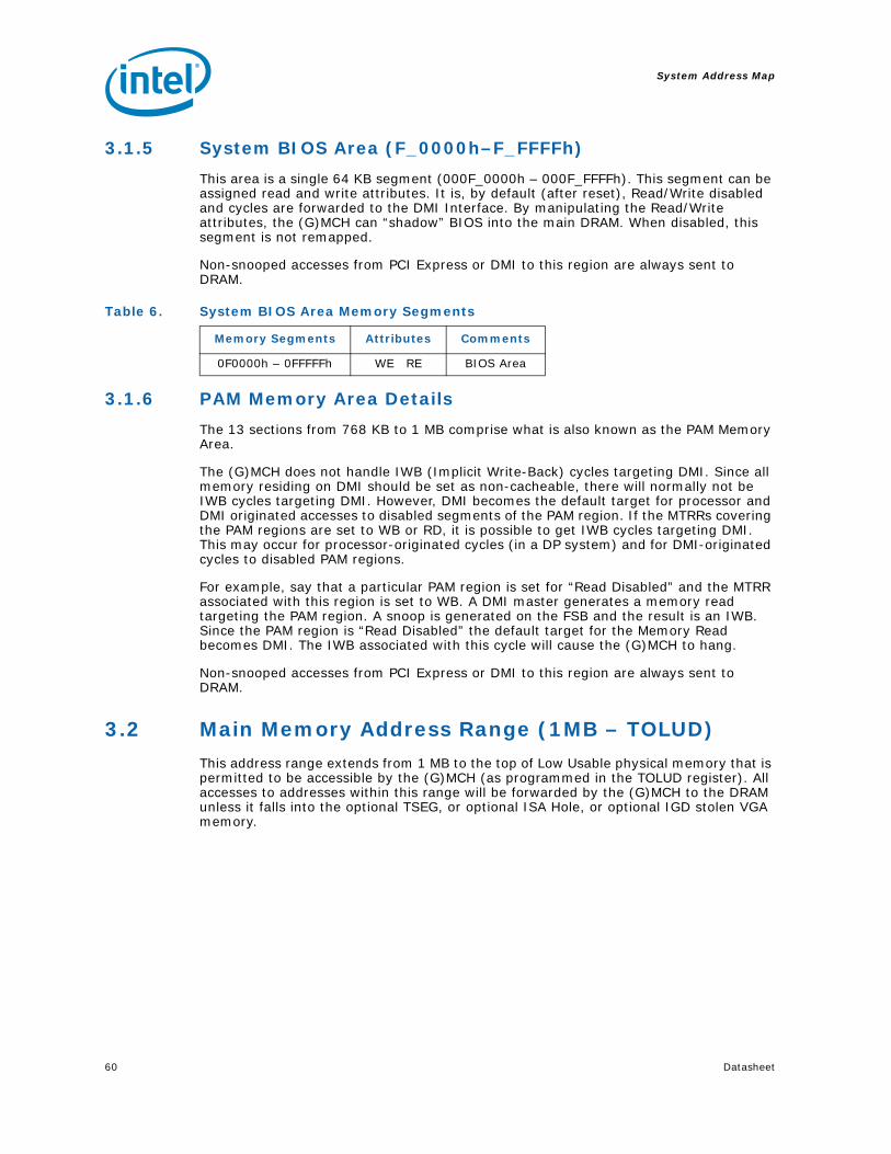
System Address Map
60 Datasheet
3.1.5 System BIOS Area (F_0000h–F_FFFFh)
This area is a single 64 KB segment (000F_0000h – 000F_FFFFh). This segment can be assigned read and write attributes. It is, by default (after reset), Read/Write disabled and cycles are forwarded to the DMI Interface. By manipulating the Read/Write attributes, the (G)MCH can “shadow” BIOS into the main DRAM. When disabled, this segment is not remapped.
Non-snooped accesses from PCI Express or DMI to this region are always sent to DRAM.
3.1.6 PAM Memory Area Details
The 13 sections from 768 KB to 1 MB comprise what is also known as the PAM Memory Area.
The (G)MCH does not handle IWB (Implicit Write-Back) cycles targeting DMI. Since all memory residing on DMI should be set as non-cacheable, there will normally not be IWB cycles targeting DMI. However, DMI becomes the default target for processor and DMI originated accesses to disabled segments of the PAM region. If the MTRRs covering the PAM regions are set to WB or RD, it is possible to get IWB cycles targeting DMI. This may occur for processor-originated cycles (in a DP system) and for DMI-originated cycles to disabled PAM regions.
For example, say that a particular PAM region is set for “Read Disabled” and the MTRR associated with this region is set to WB. A DMI master generates a memory read targeting the PAM region. A snoop is generated on the FSB and the result is an IWB. Since the PAM region is “Read Disabled” the default target for the Memory Read becomes DMI. The IWB associated with this cycle will cause the (G)MCH to hang.
Non-snooped accesses from PCI Express or DMI to this region are always sent to DRAM.
3.2 Main Memory Address Range (1MB – TOLUD)
This address range extends from 1 MB to the top of Low Usable physical memory that is permitted to be accessible by the (G)MCH (as programmed in the TOLUD register). All accesses to addresses within this range will be forwarded by the (G)MCH to the DRAM unless it falls into the optional TSEG, or optional ISA Hole, or optional IGD stolen VGA memory.
Table 6. System BIOS Area Memory Segments
Memory Segments Attributes Comments
0F0000h – 0FFFFFh WE RE BIOS Area

Datasheet 61
System Address Map
3.2.1 ISA Hole (15 MB –16 MB)
A hole can be created at 15 MB–16 MB as controlled by the fixed hole enable in Device 0 space. Accesses within this hole are forwarded to the DMI Interface. The range of physical DRAM memory disabled by opening the hole is not remapped to the top of the memory – that physical DRAM space is not accessible. This 15 MB–16 MB hole is an optionally enabled ISA hole.
Video accelerators originally used this hole. It is also used by validation and customer SV teams for some of their test cards. That is why it is being supported. There is no inherent BIOS request for the 15 MB–16 MB window.
Figure 6. Main Memory Address Range
DOS Compatibility Memory
Main Memory
ISA Hole (optional)
Main Memory
Main Memory
TSEG (1MB/2MB/8MB, optional)
PCI Memory Range
LT
FLASH
APIC
4 GB
0h
0010_0000h
00F0_0000h
0100_0000h
8 GB
FFFF_FFFFh
.
.
.
.
.
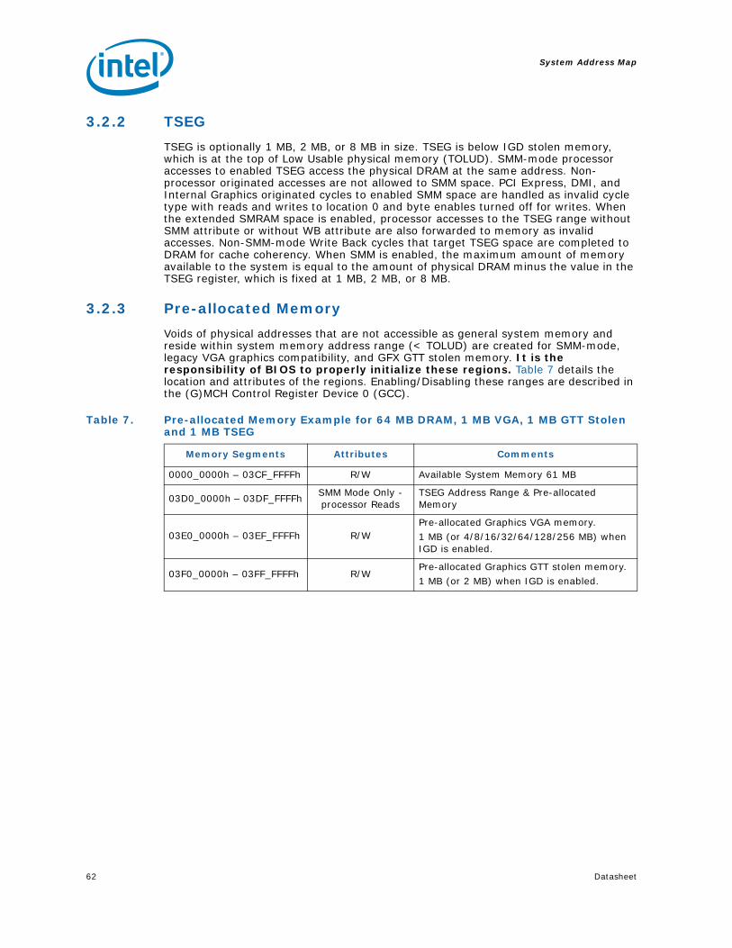
System Address Map
62 Datasheet
3.2.2 TSEG
TSEG is optionally 1 MB, 2 MB, or 8 MB in size. TSEG is below IGD stolen memory, which is at the top of Low Usable physical memory (TOLUD). SMM-mode processor accesses to enabled TSEG access the physical DRAM at the same address. Non-processor originated accesses are not allowed to SMM space. PCI Express, DMI, and Internal Graphics originated cycles to enabled SMM space are handled as invalid cycle type with reads and writes to location 0 and byte enables turned off for writes. When the extended SMRAM space is enabled, processor accesses to the TSEG range without SMM attribute or without WB attribute are also forwarded to memory as invalid accesses. Non-SMM-mode Write Back cycles that target TSEG space are completed to DRAM for cache coherency. When SMM is enabled, the maximum amount of memory available to the system is equal to the amount of physical DRAM minus the value in the TSEG register, which is fixed at 1 MB, 2 MB, or 8 MB.
3.2.3 Pre-allocated Memory
Voids of physical addresses that are not accessible as general system memory and reside within system memory address range (< TOLUD) are created for SMM-mode, legacy VGA graphics compatibility, and GFX GTT stolen memory. It is the responsibility of BIOS to properly initialize these regions. Table 7 details the location and attributes of the regions. Enabling/Disabling these ranges are described in the (G)MCH Control Register Device 0 (GCC).
Table 7. Pre-allocated Memory Example for 64 MB DRAM, 1 MB VGA, 1 MB GTT Stolen and 1 MB TSEG
Memory Segments Attributes Comments
0000_0000h – 03CF_FFFFh R/W Available System Memory 61 MB
03D0_0000h – 03DF_FFFFhSMM Mode Only - processor Reads
TSEG Address Range & Pre-allocated Memory
03E0_0000h – 03EF_FFFFh R/WPre-allocated Graphics VGA memory.1 MB (or 4/8/16/32/64/128/256 MB) when IGD is enabled.
03F0_0000h – 03FF_FFFFh R/WPre-allocated Graphics GTT stolen memory.1 MB (or 2 MB) when IGD is enabled.

Datasheet 63
System Address Map
3.3 PCI Memory Address Range (TOLUD – 4 GB)
This address range, from the top of low usable DRAM (TOLUD) to 4 GB is normally mapped to the DMI Interface.
Device 0 exceptions are:
• Addresses decoded to the egress port registers (PXPEPBAR).
• Addresses decoded to the memory mapped range for internal (G)MCH registers (GMCHBAR).
• Addresses decoded to the flat memory-mapped address spaced to access device configuration registers (PCIEXBAR).
• Addresses decoded to the registers associated with the Direct Media Interface (DMI) register memory range (DMIBAR).
With PCI Express port, there are two exceptions to this rule.
• Addresses decoded to the PCI Express Memory Window defined by the MBASE1, MLIMIT1, registers are mapped to PCI Express.
• Addresses decoded to the PCI Express prefetchable Memory Window defined by the PMBASE1, PMLIMIT1, registers are mapped to PCI Express.
In integrated graphics configurations, there are exceptions to this rule (82Q45, 82Q43, 82B43, 82G45, 82G43, 82G41 GMCH only):
1. Addresses decoded to the IGD registers and internal graphics instruction port (Function 0 MMADR, Function 1 MMADR).
2. Addresses decode to the internal graphics translation window (GMADR)
3. Addresses decode to the Internal graphics translation table (GTTADR)
In an Intel ME configuration, there are exceptions to this rule:
1. Addresses decoded to the ME Keyboard and Text MMIO range (EPKTBAR)
2. Addresses decoded to the ME HECI MMIO range (EPHECIBAR)
3. Addresses decoded to the ME HECI2 MMIO range (EPHECI2BAR)
In a Virtualization Technology (VT) enable configuration, there are exceptions to this rule (82Q45 GMCH only):
1. Addresses decoded to the memory mapped window to Graphics VT remap engine registers (GFXVTBAR)
2. Addresses decoded to the memory mapped window to DMI VC1 VT remap engine registers (DMIVC1BAR)
3. Addresses decoded to the memory mapped window to ME VT remap engine registers (VTMEBAR)
Addresses decoded to the memory mapped window to PEG/DMI VC0 VT remap engine registers (VTDPVC0BAR)
Some of the MMIO Bars may be mapped to this range or to the range above TOUUD.
There are sub-ranges within the PCI Memory address range defined as APIC Configuration Space, FSB Interrupt Space, and High BIOS Address Range. The exceptions listed above for internal graphics and the PCI Express ports MUST NOT overlap with these ranges.

System Address Map
64 Datasheet
Figure 7. PCI Memory Address Range
DMI Interface(subtractive decode)
FEF0_0000h
4 GB – 2 MB
FSB InterruptsFEE0_0000h
PCI Express Configuration Space
E000_0000h
High BIOSFFE0_0000h
FFFF_FFFFh 4 GB
4 GB – 17 MB
DMI Interface(subtractive decode)FED0_0000h
4 GB – 18 MB
Local (CPU) APICFEC8_0000h
4 GB – 19 MB
I/O APICFEC0_0000h 4 GB – 20 MB
DMI Interface(subtractive decode)
F000_0000h4 GB – 256 MB
Possible address range/
size (not ensured)
4 GB – 512 MB
DMI Interface(subtractive decode)
TOLUD
Optional HSEG FEDA_0000h to FEDB_FFFFh
BARs, Internal Graphics
ranges, PCI Express Port
could be here.
Datasheet 65
System Address Map
3.3.1 APIC Configuration Space (FEC0_0000h–FECF_FFFFh)
This range is reserved for APIC configuration space. The I/O APIC(s) usually reside in the ICH portion of the chip-set, but may also exist as stand-alone components like PXH.
The IOAPIC spaces are used to communicate with IOAPIC interrupt controllers that may be populated in the system. Since it is difficult to relocate an interrupt controller using plug-and-play software, fixed address decode regions have been allocated for them. Processor accesses to the default IOAPIC region (FEC0_0000h to FEC7_FFFFh) are always forwarded to DMI.
The (G)MCH optionally supports additional I/O APICs behind the PCI Express “Graphics” port. When enabled via the PCI Express Configuration register (Device 1 Offset 200h), the PCI Express port will positively decode a subset of the APIC configuration space – specifically FEC8_0000h through FECF_FFFFh. Memory request to this range would then be forwarded to the PCI Express port. This mode would be disabled in typical Desktop systems. When disabled, any access within entire APIC Configuration space (FEC0_0000h to FECF_FFFFh) is forwarded to DMI.
3.3.2 HSEG (FEDA_0000h–FEDB_FFFFh)
This optional segment from FEDA_0000h to FEDB_FFFFh provides a remapping window to SMM Memory. It is sometimes called the High SMM memory space. SMM-mode processor accesses to the optionally enabled HSEG are remapped to 000A_0000h–000B_FFFFh. Non-SMM-mode processor accesses to enabled HSEG are considered invalid and are terminated immediately on the FSB. The exceptions to this rule are Non-SMM-mode Write Back cycles which are remapped to SMM space to maintain cache coherency. PCI Express and DMI originated cycles to enabled SMM space are not allowed. Physical DRAM behind the HSEG transaction address is not remapped and is not accessible. All cacheline writes with WB attribute or Implicit write backs to the HSEG range are completed to DRAM like an SMM cycle.
3.3.3 FSB Interrupt Memory Space (FEE0_0000–FEEF_FFFF)
The FSB Interrupt space is the address used to deliver interrupts to the FSB. Any device on PCI Express or DMI may issue a Memory Write to 0FEEx_xxxxh. The (G)MCH will forward this Memory Write along with the data to the FSB as an Interrupt Message Transaction. The (G)MCH terminates the FSB transaction by providing the response and asserting HTRDYB. This Memory Write cycle does not go to DRAM.
3.3.4 High BIOS Area
The top 2 MB (FFE0_0000h–FFFF_FFFFh) of the PCI Memory Address Range is reserved for System BIOS (High BIOS), extended BIOS for PCI devices, and the A20 alias of the system BIOS. The processor begins execution from the High BIOS after reset. This region is mapped to DMI Interface so that the upper subset of this region aliases to 16 MB–256 KB range. The actual address space required for the BIOS is less than 2 MB but the minimum processor MTRR range for this region is 2 MB so that full 2 MB must be considered.

System Address Map
66 Datasheet
3.4 Main Memory Address Space (4 GB to TOUUD)
The (G)MCH supports 36 bit addressing. The maximum main memory size supported is 8 GB total DRAM memory. A hole between TOLUD and 4 GB occurs when main memory size approaches 4 GB or larger. As a result, TOM, and TOUUD registers and RECLAIMBASE/RECLAIMLIMIT registers become relevant.
The new reclaim configuration registers exist to reclaim lost main memory space. The greater than 32 bit reclaim handling will be handled similar to other (G)MCHs.
Upstream read and write accesses above 36-bit addressing will be treated as invalid cycles by PEG and DMI.
Top of Memory
The “Top of Memory” (TOM) register reflects the total amount of populated physical memory. This is NOT necessarily the highest main memory address (holes may exist in main memory address map due to addresses allocated for memory mapped I/O above TOM). TOM is used to allocate the Intel Management Engine's stolen memory. The Intel ME stolen size register reflects the total amount of physical memory stolen by the Intel ME. The ME stolen memory is located at the top of physical memory. The ME stolen memory base is calculated by subtracting the amount of memory stolen by the Intel ME from TOM.
The Top of Upper Usable Dram (TOUUD) register reflects the total amount of addressable DRAM. If reclaim is disabled, TOUUD will reflect TOM minus Intel ME stolen size. If reclaim is enabled, then it will reflect the reclaim limit. Also, the reclaim base will be the same as TOM minus ME stolen memory size to the nearest 64 MB alignment.
TOLUD register is restricted to 4 GB memory (A[31:20]), but the (G)MCH can support up to 16 GB, limited by DRAM pins. For physical memory greater than 4 GB, the TOUUD register helps identify the address range in between the 4 GB boundary and the top of physical memory. This identifies memory that can be directly accessed (including reclaim address calculation) which is useful for memory access indication, early path indication, and trusted read indication. When reclaim is enabled, TOLUD must be 64 MB aligned, but when reclaim is disabled, TOLUD can be 1 MB aligned.
C1DRB3 cannot be used directly to determine the effective size of memory as the values programmed in the DRBs depend on the memory mode (stacked, interleaved). The Reclaim Base/Limit registers also can not be used because reclaim can be disabled. The C0DRB3 register is used for memory channel identification (channel 0 vs. channel 1) in the case of stacked memory.

Datasheet 67
System Address Map
3.4.1 Memory Re-claim Background
The following are examples of Memory Mapped IO devices are typically located below 4 GB:
• High BIOS
• HSEG
• TSEG
• GFX stolen
• GTT stolen
• XAPIC
• Local APIC
• FSB Interrupts
• Mbase/Mlimit
• Memory Mapped I/O space that supports only 32-bit addressing
The (G)MCH provides the capability to re-claim the physical memory overlapped by the Memory Mapped I/O logical address space. The (G)MCH re-maps physical memory from the Top of Low Memory (TOLUD) boundary up to the 4 GB boundary to an equivalent sized logical address range located just below the Intel ME's stolen memory.
3.4.2 Memory Reclaiming
An incoming address (referred to as a logical address) is checked to see if it falls in the memory re-map window. The bottom of the re-map window is defined by the value in the RECLAIMBASE register. The top of the re-map window is defined by the value in the RECLAIMLIMIT register. An address that falls within this window is reclaimed to the physical memory starting at the address defined by the TOLUD register. The TOLUD register must be 64 MB aligned when RECLAIM is enabled, but can be 1 MB aligned when reclaim is disabled.
3.5 PCI Express* Configuration Address Space
There is a device 0 register, PCIEXBAR, which defines the base address for the configuration space associated with all devices and functions that are potentially a part of the PCI Express root complex hierarchy. The size of this range will be programmable for the (G)MCH. BIOS must assign this address range such that it will not conflict with any other address ranges.

System Address Map
68 Datasheet
3.6 PCI Express* Address Space
The (G)MCH can be programmed to direct memory accesses to the PCI Express interface when addresses are within either of two ranges specified via registers in (G)MCH’s Device 1 configuration space.
• The first range is controlled via the Memory Base Register (MBASE) and Memory Limit Register (MLIMIT) registers.
• The second range is controlled via the Pre-fetchable Memory Base (PMBASE) and Pre-fetchable Memory Limit (PMLIMIT) registers.
Conceptually, address decoding for each range follows the same basic concept. The top 12 bits of the respective Memory Base and Memory Limit registers correspond to address bits A[31:20] of a memory address. For the purpose of address decoding, the (G)MCH assumes that address bits A[19:0] of the memory base are zero and that address bits A[19:0] of the memory limit address are FFFFFh. This forces each memory address range to be aligned to 1MB boundary and to have a size granularity of 1 MB.
The (G)MCH positively decodes memory accesses to PCI Express memory address space as defined by the following equations:
Memory_Base_Address ≤ Address ≤ Memory_Limit_Address
Prefetchable_Memory_Base_Address ≤ Address ≤ Prefetchable_Memory_Limit_Address
The window size is programmed by the plug-and-play configuration software. The window size depends on the size of memory claimed by the PCI Express device. Normally, these ranges will reside above the Top-of-Low Usable-DRAM and below High BIOS and APIC address ranges. They MUST reside above the top of low memory (TOLUD) if they reside below 4 GB and MUST reside above top of upper memory (TOUUD) if they reside above 4 GB or they will steal physical DRAM memory space.
It is essential to support a separate Pre-fetchable range in order to apply USWC attribute (from the processor point of view) to that range. The USWC attribute is used by the processor for write combining.
Note that the (G)MCH Device 1 memory range registers described above are used to allocate memory address space for any PCI Express devices sitting on PCI Express that require such a window.
The PCICMD1 register can override the routing of memory accesses to PCI Express. In other words, the memory access enable bit must be set in the device 1 PCICMD1 register to enable the memory base/limit and pre-fetchable base/limit windows.
For the (G)MCH, the upper PMUBASE1/PMULIMIT1 registers have been implemented for PCI Express Spec compliance. The (G)MCH locates MMIO space above 4 GB using these registers.

Datasheet 69
System Address Map
3.7 Graphics Memory Address Ranges (Intel® 82Q45, 82Q43, 82B43, 82G45, 82G43, 82G41 GMCH Only)
The GMCH can be programmed to direct memory accesses to IGD when addresses are within any of five ranges specified via registers in GMCH’s Device 2 configuration space.
1. The Memory Map Base Register (MMADR) is used to access graphics control registers.
2. The Graphics Memory Aperture Base Register (GMADR) is used to access graphics memory allocated via the graphics translation table.
3. The Graphics Translation Table Base Register (GTTADR) is used to access the translation table.
These ranges can reside above the Top-of-Low-DRAM and below High BIOS and APIC address ranges. They MUST reside above the top of memory (TOLUD) and below 4 GB so they do not steal any physical DRAM memory space.
GMADR is a Prefetchable range in order to apply USWC attribute (from the processor point of view) to that range. The USWC attribute is used by the processor for write combining.
3.8 System Management Mode (SMM)
System Management Mode uses main memory for System Management RAM (SMM RAM). The (G)MCH supports: Compatible SMRAM (C_SMRAM), High Segment (HSEG), and Top of Memory Segment (TSEG). System Management RAM space provides a memory area that is available for the SMI handlers and code and data storage. This memory resource is normally hidden from the system OS so the processor has immediate access to this memory space upon entry to SMM. The (G)MCH provides three SMRAM options:
• Below 1 MB option that supports compatible SMI handlers.• Above 1 MB option that allows new SMI handlers to execute with write-back
cacheable SMRAM. • Optional TSEG area of 1 MB, 2 MB, or 8 MB in size. For the 82Q45, 82Q43, 82B43,
82G45, 82G43, 82G41 GMCH, TSEG area lies below IGD stolen memory.
The above 1 MB solutions require changes to compatible SMRAM handlers code to properly execute above 1 MB.
Note: DMI Interface and PCI Express masters are not allowed to access the SMM space.
3.8.1 SMM Space Definition
SMM space is defined by its addressed SMM space and its DRAM SMM space. The addressed SMM space is defined as the range of bus addresses used by the processor to access SMM space. DRAM SMM space is defined as the range of physical DRAM memory locations containing the SMM code. SMM space can be accessed at one of three transaction address ranges: Compatible, High, and TSEG. The Compatible and TSEG SMM space is not remapped; therefore, the addressed and DRAM SMM space is the same address range. Since the High SMM space is remapped the addressed and DRAM SMM space is a different address range. Note that the High DRAM space is the same as the Compatible Transaction Address space. Table 8 describes three unique address ranges:
• Compatible Transaction Address • High Transaction Address • TSEG Transaction Address

System Address Map
70 Datasheet
3.8.2 SMM Space Restrictions
If any of the following conditions are violated the results of SMM accesses are unpredictable and may cause the system to hang:
1. The Compatible SMM space must not be set-up as cacheable.
2. High or TSEG SMM transaction address space must not overlap address space assigned to system DRAM, or to any “PCI” devices (including DMI Interface, and PCI-Express, and graphics devices). This is a BIOS responsibility.
3. Both D_OPEN and D_CLOSE must not be set to 1 at the same time.
4. When TSEG SMM space is enabled, the TSEG space must not be reported to the OS as available DRAM. This is a BIOS responsibility.
5. Any address translated through the GMADR TLB must not target DRAM from A_0000-F_FFFF.
3.8.3 SMM Space Combinations
When High SMM is enabled (G_SMRAME=1 and H_SMRAM_EN=1), the Compatible SMM space is effectively disabled. Processor-originated accesses to the Compatible SMM space are forwarded to PCI Express if VGAEN=1 (also depends on MDAP), otherwise they are forwarded to the DMI Interface. PCI Express and DMI Interface originated accesses are never allowed to access SMM space.
3.8.4 SMM Control Combinations
The G_SMRAME bit provides a global enable for all SMM memory. The D_OPEN bit allows software to write to the SMM ranges without being in SMM mode. BIOS software can use this bit to initialize SMM code at powerup. The D_LCK bit limits the SMM range access to only SMM mode accesses. The D_CLS bit causes SMM (both CSEG and TSEG) data accesses to be forwarded to the DMI Interface or PCI Express. The SMM software can use this bit to write to video memory while running SMM code out of DRAM.
Table 8. Transaction Address Ranges – Compatible, High, and TSEG
SMM Space Enabled Transaction Address Space DRAM Space (DRAM)
Compatible 000A_0000h to 000B_FFFFh 000A_0000h to 000B_FFFFh
High FEDA_0000h to FEDB_FFFFh 000A_0000h to 000B_FFFFh
TSEG (TOLUD–STOLEN–TSEG) to
TOLUD–STOLEN(TOLUD–STOLEN–TSEG) to
TOLUD–STOLEN
Table 9. SMM Space Table
Global Enable G_SMRAME
High Enable H_SMRAM_EN
TSEG Enable TSEG_EN
Compatible (C) Range
High (H) Range
TSEG (T) Range
0 X X Disable Disable Disable
1 0 0 Enable Disable Disable
1 0 1 Enable Disable Enable
1 1 0 Disabled Enable Disable
1 1 1 Disabled Enable Enable

Datasheet 71
System Address Map
3.8.5 SMM Space Decode and Transaction Handling
Only the processor is allowed to access SMM space. PCI Express and DMI Interface originated transactions are not allowed to SMM space.
3.8.6 Processor WB Transaction to an Enabled SMM Address Space
Processor Writeback transactions (REQa[1]# = 0) to enabled SMM Address Space must be written to the associated SMM DRAM even though D_OPEN=0 and the transaction is not performed in SMM mode. This ensures SMM space cache coherency when cacheable extended SMM space is used.
3.8.7 SMM Access Through GTT TLB (Intel® 82Q45, 82Q43, 82B43, 82G45, 82G43, 82G41 GMCH Only)
Accesses through GTT TLB address translation to enabled SMM DRAM space are not allowed. Writes will be routed to Memory address 000C_0000h with byte enables de-asserted and reads will be routed to Memory address 000C_0000h. If a GTT TLB translated address hits enabled SMM DRAM space, an error is recorded.
PCI Express and DMI Interface originated accesses are never allowed to access SMM space directly or through the GTT TLB address translation. If a GTT TLB translated address hits enabled SMM DRAM space, an error is recorded.
PCI Express and DMI Interface write accesses through GMADR range will be snooped. Assesses to GMADR linear range (defined via fence registers) are supported. PCI Express and DMI Interface tileY and tileX writes to GMADR are not supported. If, when translated, the resulting physical address is to enabled SMM DRAM space, the request will be remapped to address 000C_0000h with de-asserted byte enables.
PCI Express and DMI Interface read accesses to the GMADR range are not supported therefore will have no address translation concerns. PCI Express and DMI Interface reads to GMADR will be remapped to address 000C_0000h. The read will complete with UR (unsupported request) completion status.
Table 10. SMM Control Table
G_SMRAME D_LCK D_CLS D_OPENProcessor
in SMM Mode
SMM Code Access
SMM Data Access
0 x X x x Disable Disable
1 0 X 0 0 Disable Disable
1 0 0 0 1 Enable Enable
1 0 0 1 x Enable Enable
1 0 1 0 1 Enable Disable
1 0 1 1 x Invalid Invalid
1 1 X x 0 Disable Disable
1 1 0 x 1 Enable Enable
1 1 1 x 1 Enable Disable

System Address Map
72 Datasheet
GTT Fetches are always decoded (at fetch time) to ensure not in SMM (actually, anything above base of TSEG or 640 KB–1 MB). Thus, they will be invalid and go to address 000C_0000h, but that is not specific to PCI Express or DMI; it applies to processor or internal graphics engines. Also, since the GMADR snoop would not be directly to the SMM space, there wouldn’t be a writeback to SMM. In fact, the writeback would also be invalid (because it uses the same translation) and go to address 000C_0000h.
3.9 Memory Shadowing
Any block of memory that can be designated as read-only or write-only can be “shadowed” into (G)MCH DRAM memory. Typically this is done to allow ROM code to execute more rapidly out of main DRAM. ROM is used as a read-only during the copy process while DRAM at the same time is designated write-only. After copying, the DRAM is designated read-only so that ROM is shadowed. Processor bus transactions are routed accordingly.
3.10 I/O Address Space
The (G)MCH does not support the existence of any other I/O devices beside itself on the processor bus. The (G)MCH generates either DMI Interface or PCI Express bus cycles for all processor I/O accesses that it does not claim. Within the host bridge, the (G)MCH contains two internal registers in the processor I/O space, Configuration Address Register (CONFIG_ADDRESS) and the Configuration Data Register (CONFIG_DATA). These locations are used to implement configuration space access mechanism.
The processor allows 64 K+3 bytes to be addressed within the I/O space. The (G)MCH propagates the processor I/O address without any translation on to the destination bus and therefore provides addressability for 64K+3 byte locations. Note that the upper 3 locations can be accessed only during I/O address wrap-around when processor bus HAB_16 address signal is asserted. HAB_16 is asserted on the processor bus whenever an I/O access is made to 4 bytes from address 0FFFDh, 0FFFEh, or 0FFFFh. HAB_16 is also asserted when an I/O access is made to 2 bytes from address 0FFFFh.
A set of I/O accesses (other than ones used for configuration space access) are consumed by the internal graphics device if it is enabled. The mechanisms for internal graphics I/O decode and the associated control is explained later.
The I/O accesses (other than ones used for configuration space access) are forwarded normally to the DMI Interface bus unless they fall within the PCI Express I/O address range as defined by the mechanisms explained below. I/O writes are NOT posted. Memory writes to ICH or PCI Express are posted. The PCICMD1 register can disable the routing of I/O cycles to the PCI Express.
The (G)MCH responds to I/O cycles initiated on PCI Express or DMI with an UR status. Upstream I/O cycles and configuration cycles should never occur. If one does occur, the request will route as a read to Memory address 000C_0000h so a completion is naturally generated (whether the original request was a read or write). The transaction will complete with an UR completion status.
I/O reads that lie within 8-byte boundaries but cross 4-byte boundaries are issued from the processor as 1 transaction. The (G)MCH will break this into 2 separate transactions. I/O writes that lie within 8-byte boundaries but cross 4-byte boundaries are assumed to be split into 2 transactions by the processor.

Datasheet 73
System Address Map
3.10.1 PCI Express* I/O Address Mapping
The (G)MCH can be programmed to direct non-memory (I/O) accesses to the PCI Express bus interface when processor initiated I/O cycle addresses are within the PCI Express I/O address range. This range is controlled via the I/O Base Address (IOBASE) and I/O Limit Address (IOLIMIT) registers in (G)MCH Device 1 configuration space.
Address decoding for this range is based on the following concept. The top 4 bits of the respective I/O Base and I/O Limit registers correspond to address bits A[15:12] of an I/O address. For the purpose of address decoding, the (G)MCH assumes that lower 12 address bits A[11:0] of the I/O base are zero and that address bits A[11:0] of the I/O limit address are FFFh. This forces the I/O address range alignment to 4 KB boundary and produces a size granularity of 4 KB.
The (G)MCH positively decodes I/O accesses to PCI Express I/O address space as defined by the following equation:
I/O_Base_Address ≤ Processor I/O Cycle Address ≤ I/O_Limit_Address
The effective size of the range is programmed by the plug-and-play configuration software and it depends on the size of I/O space claimed by the PCI Express device.
The (G)MCH also forwards accesses to the Legacy VGA I/O ranges according to the settings in the Device #1 configuration registers BCTRL (VGA Enable) and PCICMD1 (IOAE1), unless a second adapter (monochrome) is present on the DMI Interface/PCI (or ISA). The presence of a second graphics adapter is determined by the MDAP configuration bit. When MDAP is set, the (G)MCH will decode legacy monochrome I/O ranges and forward them to the DMI Interface. The IO ranges decoded for the monochrome adapter are 3B4h, 3B5h, 3B8h, 3B9h, 3BAh, and 3BFh.
Note that the (G)MCH Device 1 and/or Device 6 I/O address range registers defined above are used for all I/O space allocation for any devices requiring it (such a window on PCI Express).
The PCICMD1 register can disable the routing of I/O cycles to PCI Express.
3.11 (G)MCH Decode Rules and Cross-Bridge Address Mapping
VGAA = 000A_0000 – 000A_FFFFMDA = 000B_0000 – 000B_7FFFVGAB = 000B_8000 – 000B_FFFFMAINMEM = 0100_0000 to TOLUDHIGHMEM = 4 GB to TOMRECLAIMMEM = RECLAIMBASE to RECLAIMLIMIT
3.11.1 Legacy VGA and I/O Range Decode Rules
The legacy 128 KB VGA memory range 000A_0000h-000B_FFFFh can be mapped to IGD (Device 2), to PCI Express (Device 1), and/or to the DMI Interface depending on the programming of the VGA steering bits. Priority for VGA mapping is constant in that the (G)MCH always decodes internally mapped devices first. Internal to the (G)MCH, decode precedence is always given to IGD. The (G)MCH always positively decodes internally mapped devices, namely the IGD and PCI-Express. Subsequent decoding of regions mapped to PCI Express or the DMI Interface depends on the Legacy VGA configurations bits (VGA Enable and MDAP).
§ §

System Address Map
74 Datasheet

Datasheet 75
Register Description
4 Register Description
The (G)MCH contains two sets of software accessible registers, accessed via the Host processor I/O address space: Control registers and internal configuration registers.
• Control registers are I/O mapped into the processor I/O space, which control access to PCI and PCI Express configuration space (see Section 4.5).
• Internal configuration registers residing within the (G)MCH are partitioned into logical device register sets (“logical” since they reside within a single physical device). One register set is dedicated to Host Bridge functionality (i.e., DRAM configuration, other chip-set operating parameters and optional features). Another register set is dedicated to Host-PCI Express Bridge functions (controls PCI Express interface configurations and operating parameters). The 82P45 has a second register set devoted to Host-PCI Express Bridge functions. There is also a register sets devoted to Management Engine (ME) Control. For the 82Q45, 82Q43, 82B43, 82G45, 82G43, 82G41 GMCH, a register set is for the internal graphics functions. The 82Q45 GMCH has register sets devoted to Intel Trusted Execution Technology and Intel Virtualization Technology.
The (G)MCH internal registers (I/O Mapped, Configuration and PCI Express Extended Configuration registers) are accessible by the Host processor. The registers that reside within the lower 256 bytes of each device can be accessed as Byte, Word (16 bit), or DWord (32 bit) quantities, with the exception of CONFIG_ADDRESS, which can only be accessed as a Dword. All multi-byte numeric fields use "little-endian" ordering (i.e., lower addresses contain the least significant parts of the field). Registers which reside in bytes 256 through 4095 of each device may only be accessed using memory mapped transactions in Dword (32 bit) quantities.
Some of the (G)MCH registers described in this section contain reserved bits. These bits are labeled "Reserved”. Software must deal correctly with fields that are reserved. On reads, software must use appropriate masks to extract the defined bits and not rely on reserved bits being any particular value. On writes, software must ensure that the values of reserved bit positions are preserved. That is, the values of reserved bit positions must first be read, merged with the new values for other bit positions and then written back. Note the software does not need to perform read, merge, and write operation for the Configuration Address Register.
In addition to reserved bits within a register, the (G)MCH contains address locations in the configuration space of the Host Bridge entity that are marked either "Reserved" or “Intel Reserved”. The (G)MCH responds to accesses to “Reserved” address locations by completing the host cycle. When a “Reserved” register location is read, a zero value is returned. (“Reserved” registers can be 8-, 16-, or 32 bits in size). Writes to “Reserved” registers have no effect on the (G)MCH. Registers that are marked as “Intel Reserved” must not be modified by system software. Writes to “Intel Reserved” registers may cause system failure. Reads from “Intel Reserved” registers may return a non-zero value.
Upon a Full Reset, the (G)MCH sets its entire set of internal configuration registers to predetermined default states. Some register values at reset are determined by external strapping options. The default state represents the minimum functionality feature set required to successfully bringing up the system. Hence, it does not represent the optimal system configuration. It is the responsibility of the system initialization software (usually BIOS) to properly determine the DRAM configurations, operating parameters and optional system features that are applicable, and to program the (G)MCH registers accordingly.

Register Description
76 Datasheet
4.1 Register Terminology
The following table shows the register-related terminology that is used.
Item Definition
RORead Only bit(s). Writes to these bits have no effect. This may be a status bit or a static value.
RO/S
Read Only / Sticky bit(s). Writes to these bits have no effect. These are status bits only. Bits are not returned to their default values by "warm" reset, but will be reset with a cold/complete reset (for PCI Express related bits a cold reset is “Power Good Reset” as defined in the PCI Express spec).
RS/WC
Read Set / Write Clear bit(s).The first time the bit is read with an enabled byte, it returns the value 0, but a side-effect of the read is that the value changes to 1. Any subsequent reads with enabled bytes return a 1 until a 1 is written to the bit. When the bit is read, but the byte is not enabled, the state of the bit does not change, and the value returned is irrelevant, but will match the state of the bit.When a 0 is written to the bit, there is no effect. When a 1 is written to the bit, its value becomes 0, until the next byte-enabled read. When the bit is written, but the byte is not enabled, there is no effect.
R/WRead / Write bit(s). These bits can be read and written by software. Hardware may only change the state of this bit by reset.
R/WCRead / Write Clear bit(s). These bits can be read. Internal events may set this bit. A software write of ‘1’ clears (sets to ‘0’) the corresponding bit(s) and a write of ‘0’ has no effect.
R/WC/S
Read / Write Clear / Sticky bit(s). These bits can be read. Internal events may set this bit. A software write of ‘1’ clears (sets to ‘0’) the corresponding bit(s) and a write of ‘0’ has no effect. Bits are not cleared by "warm" reset, but will be reset with a cold/complete reset (for PCI Express related bits a cold reset is “Power Good Reset” as defined in the PCI Express spec).
R/W/KRead / Write / Key bit(s). These bits can be read and written by software. Additionally this bit, when set, prohibits some other bit field(s) from being writeable (bit fields become Read Only).
R/W/L
Read / Write / Lockable bit(s). These bits can be read and written by software. Additionally, there is a Key bit (which is marked R/W/K or R/W/L/K) that, when set, prohibits this bit field from being writeable (bit field becomes Read Only).
R/W/S
Read / Write / Sticky bit(s). These bits can be read and written by software. Bits are not cleared by "warm" reset, but will be reset with a cold/complete reset (for PCI Express related bits a cold reset is “Power Good Reset” as defined in the PCI Express spec).
R/W/SC
Read / Write / Self Clear bit(s). These bits can be read and written by software. When the bit is 1, hardware may clear the bit to ‘0’ based upon internal events, possibly sooner than any subsequent software read could retrieve a 1.

Datasheet 77
Register Description
4.2 Configuration Process and Registers
4.2.1 Platform Configuration Structure
The DMI physically connects the (G)MCH and the Intel ICH10/ICH7; so, from a configuration standpoint, the DMI is logically PCI bus 0. As a result, all devices internal to the (G)MCH and the Intel ICH10/ICH7 appear to be on PCI bus 0.
The ICH10/ICH7 internal LAN controller does not appear on bus 0 – it appears on the external PCI bus (whose number is configurable).
The system’s primary PCI expansion bus is physically attached to the Intel ICH10/ICH7 and, from a configuration perspective, appears to be a hierarchical PCI bus behind a PCI-to-PCI bridge and therefore has a programmable PCI Bus number. The PCI Express Graphics Attach appears to system software to be a real PCI bus behind a PCI-to-PCI bridge that is a device resident on PCI bus 0.
A physical PCI bus 0 does not exist and that DMI and the internal devices in the (G)MCH and Intel ICH10/ICH7 logically constitute PCI Bus 0 to configuration software. This is shown in the following figure.
The (G)MCH contains the following PCI devices within a single physical component. The configuration registers for the four devices are mapped as devices residing on PCI bus 0.
• Device 0: Host Bridge/DRAM Controller. Logically this appears as a PCI device residing on PCI bus 0. Device 0 contains the standard PCI header registers, PCI Express base address register, DRAM control (including thermal/throttling control), configuration for the DMI, and other (G)MCH specific registers.
• Device 1: Host-PCI Express Bridge. Logically this appears as a “virtual” PCI-to-PCI bridge residing on PCI bus 0 and is compliant with PCI Express Specification Revision 1.0. Device 1 contains the standard PCI-to-PCI bridge registers and the standard PCI Express/PCI configuration registers (including the PCI Express memory address mapping). It also contains Isochronous and Virtual Channel controls in the PCI Express extended configuration space.
• Device 2: Internal Graphics Control (82Q45, 82Q43, 82B43, 82G45, 82G43, 82G41 GMCH only). Logically, this appears as a PCI device residing on PCI bus #0. Physically, device 2 contains the configuration registers for 3D, 2D, and display functions.
• Device 3: Management Engine Control. ME control.
R/W/SC/L
Read / Write / Self Clear / Lockable bit(s). These bits can be read and written by software. When the bit is ‘1’, hardware may clear the bit to ‘0’ based upon internal events, possibly sooner than any subsequent software read could retrieve a ‘1’. Additionally there is a bit (which is marked R/W/K or R/W/L/K) that, when set, prohibits this bit field from being writeable (bit field becomes Read Only).
R/WO
Write Once bit(s). Once written by software, bits with this attribute become Read Only. These bits can only be cleared by a Reset. If there are multiple R/WO fields within a DWord, they should be written all at once (atomically) to avoid capturing an incorrect value.
WWrite Only. These bits may be written by software, but will always return zeros when read. They are used for write side-effects. Any data written to these registers cannot be retrieved.
Item Definition

Register Description
78 Datasheet
• Device 6: Secondary Host-PCI Express Bridge. (82P45 MCH only). Logically this appears as a “virtual” PCI-to-PCI bridge residing on PCI bus 0 and is compliant with PCI Express Specification Revision 1.0. Device 6 contains the standard PCI-to-PCI bridge registers and the standard PCI Express/PCI configuration registers (including the PCI Express memory address mapping). It also contains Isochronous and Virtual Channel controls in the PCI Express extended configuration space.
4.3 Configuration Mechanisms
The processor is the originator of configuration cycles so the FSB is the only interface in the platform where these mechanisms are used. Internal to the (G)MCH transactions received through both configuration mechanisms are translated to the same format.
4.3.1 Standard PCI Configuration Mechanism
The following is the mechanism for translating processor I/O bus cycles to configuration cycles.
The PCI specification defines a slot based "configuration space" that allows each device to contain up to 8 functions with each function containing up to 256 8-bit configuration registers. The PCI specification defines two bus cycles to access the PCI configuration space: Configuration Read and Configuration Write. Memory and I/O spaces are supported directly by the processor. Configuration space is supported by a mapping mechanism implemented within the (G)MCH.
The configuration access mechanism makes use of the CONFIG_ADDRESS Register (at I/O address 0CF8h though 0CFBh) and CONFIG_DATA Register (at I/O address 0CFCh though 0CFFh). To reference a configuration register a DW I/O write cycle is used to place a value into CONFIG_ADDRESS that specifies the PCI bus, the device on that bus, the function within the device and a specific configuration register of the device function being accessed. CONFIG_ADDRESS[31] must be 1 to enable a configuration cycle. CONFIG_DATA then becomes a window into the four bytes of configuration space specified by the contents of CONFIG_ADDRESS. Any read or write to CONFIG_DATA will result in the (G)MCH translating the CONFIG_ADDRESS into the appropriate configuration cycle.
The (G)MCH is responsible for translating and routing the processor’s I/O accesses to the CONFIG_ADDRESS and CONFIG_DATA registers to internal (G)MCH configuration registers, DMI or PCI Express.
4.3.2 PCI Express* Enhanced Configuration Mechanism
PCI Express extends the configuration space to 4096 bytes per device/function as compared to 256 bytes allowed by the PCI Specification, Revision 2.3. PCI Express configuration space is divided into a PCI 2.3 compatible region, which consists of the first 256B of a logical device’s configuration space and a PCI Express extended region which consists of the remaining configuration space.
The PCI compatible region can be accessed using either the Standard PCI Configuration Mechanism or using the PCI Express Enhanced Configuration Mechanism described in this section. The extended configuration registers may only be accessed using the PCI Express Enhanced Configuration Mechanism. To maintain compatibility with PCI configuration addressing mechanisms, system software must access the extended configuration space using 32-bit operations (32-bit aligned) only. These 32-bit operations include byte enables allowing only appropriate bytes within the DWord to be accessed. Locked transactions to the PCI Express memory mapped configuration address space are not supported. All changes made using either access mechanism are equivalent.

Datasheet 79
Register Description
The PCI Express Enhanced Configuration Mechanism utilizes a flat memory-mapped address space to access device configuration registers. This address space is reported by the system firmware to the operating system. There is a register, PCIEXBAR, that defines the base address for the block of addresses below 4 GB for the configuration space associated with busses, devices and functions that are potentially a part of the PCI Express root complex hierarchy. In the PCIEXBAR register there exists controls to limit the size of this reserved memory mapped space. 256 MB is the amount of address space required to reserve space for every bus, device, and function that could possibly exist. Options for 128 MB and 64 MB exist in order to free up those addresses for other uses. In these cases the number of busses and all of their associated devices and functions are limited to 128 or 64 busses respectively.
The PCI Express Configuration Transaction Header includes an additional 4 bits (ExtendedRegisterAddress[3:0]) between the Function Number and Register Address fields to provide indexing into the 4 KB of configuration space allocated to each potential device. For PCI Compatible Configuration Requests, the Extended Register Address field must be all zeros.
Just the same as with PCI devices, each device is selected based on decoded address information that is provided as a part of the address portion of Configuration Request packets. A PCI Express device will decode all address information fields (bus, device, function and extended address numbers) to provide access to the correct register.
To access this space (steps 1, 2, 3 are done only once by BIOS),
1. Use the PCI compatible configuration mechanism to enable the PCI Express enhanced configuration mechanism by writing 1 to bit 0 of the PCIEXBAR register.
2. Use the PCI compatible configuration mechanism to write an appropriate PCI Express base address into the PCIEXBAR register
3. Calculate the host address of the register you wish to set using (PCI Express base + (bus number * 1 MB) + (device number * 32KB) + (function number * 4 KB) + (1 B * offset within the function) = host address)
4. Use a memory write or memory read cycle to the calculated host address to write or read that register.
Figure 8. Memory Map to PCI Express Device Configuration Space
Bus 255
FFFFFFFh
Bus 1
Bus 0
1FFFFFh
FFFFFh
0h
Device 31
FFFFFh
Device 1
Device 0
FFFFh
7FFFh
Function 7
7FFFh
Function 1
Function 0
1FFFh
FFFh
FFFh
PCI Compatible
Config Space
PCI Compatible
Config Header
FFh
3Fh
PCI Express* Extended
Configuration Space
Located By PCI Express* Base
Address

Register Description
80 Datasheet
4.4 Routing Configuration Accesses
The (G)MCH supports two PCI related interfaces: DMI and PCI Express. The (G)MCH is responsible for routing PCI and PCI Express configuration cycles to the appropriate device that is an integrated part of the (G)MCH or to one of these two interfaces. Configuration cycles to the ICH10/ICH7 internal devices and Primary PCI (including downstream devices) are routed to the ICH10/ICH7 via DMI. Configuration cycles to both the PCI Express Graphics PCI compatibility configuration space and the PCI Express Graphics extended configuration space are routed to the PCI Express Graphics port device or associated link.
Figure 9. MCH Configuration Cycle Flow Chart
DW I/O Write toCONFIG_ADDRESS
with bit 31 = 1
I/O Read/Write toCONFIG_DATA
MCH Generates Type 1 Access to PCI Express
MCH allows cycle to go to DMI resulting in Master Abort
Bus# > SEC BUSBus# ≤ SUB BUS
in MCH Dev 1
Bus# = 0
Device# = 1 &Dev # 1 Enabled& Function# = 0
Device# = 0 &Function# = 0
MCH GeneratesDMI Type 1
Configuration Cycle
Bus# =SECONDARYBUS
in MCH Dev 1
MCH Claims
MCH Claims
Yes
No
Yes
Yes
No
No
Yes
Yes
No
No
Device# = 0 MCH GeneratesType 0 Accessto PCI Express
Yes
MCH GeneratesDMI Type 0
Configuration Cycle
No

Datasheet 81
Register Description
4.4.1 Internal Device Configuration Accesses
The (G)MCH decodes the Bus Number (bits 23:16) and the Device Number fields of the CONFIG_ADDRESS register. If the Bus Number field of CONFIG_ADDRESS is 0 the configuration cycle is targeting a PCI Bus 0 device.
If the targeted PCI Bus 0 device exists in the (G)MCH and is not disabled, the configuration cycle is claimed by the appropriate device.
4.4.2 Bridge Related Configuration Accesses
Configuration accesses on PCI Express or DMI are PCI Express Configuration TLPs.
• Bus Number [7:0] is Header Byte 8 [7:0]
• Device Number [4:0] is Header Byte 9 [7:3]
• Function Number [2:0] is Header Byte 9 [2:0]
And special fields for this type of TLP:
• Extended Register Number [3:0] is Header Byte 10 [3:0]
• Register Number [5:0] is Header Byte 11 [7:2]
See the PCI Express specification for more information on both the PCI 2.3 compatible and PCI Express Enhanced Configuration Mechanism and transaction rules.
4.4.2.1 PCI Express* Configuration Accesses
When the Bus Number of a type 1 Standard PCI Configuration cycle or PCI Express Enhanced Configuration access matches the Device 1 Secondary Bus Number a PCI Express Type 0 Configuration TLP is generated on the PCI Express link targeting the device directly on the opposite side of the link. This should be Device 0 on the bus number assigned to the PCI Express link (likely Bus 1).
The device on other side of link must be Device 0. The (G)MCH will Master Abort any Type 0 Configuration access to a non-zero Device number. If there is to be more than one device on that side of the link there must be a bridge implemented in the downstream device.
When the Bus Number of a type 1 Standard PCI Configuration cycle or PCI Express Enhanced Configuration access is within the claimed range (between the upper bound of the bridge device’s Subordinate Bus Number register and the lower bound of the bridge device’s Secondary Bus Number register) but does not match the Device 1 Secondary Bus Number, a PCI Express Type 1 Configuration TLP is generated on the secondary side of the PCI Express link.
PCI Express Configuration Writes:
• Internally the host interface unit will translate writes to PCI Express extended configuration space to configuration writes on the backbone.
• Writes to extended space are posted on the FSB, but non-posted on the PCI Express or DMI (i.e., translated to config writes)

Register Description
82 Datasheet
4.4.2.2 DMI Configuration Accesses
Accesses to disabled (G)MCH internal devices, bus numbers not claimed by the Host-PCI Express bridge, or PCI Bus 0 devices not part of the (G)MCH will subtractively decode to the ICH10/ICH7 and consequently be forwarded over the DMI via a PCI Express configuration TLP.
If the Bus Number is zero, the (G)MCH will generate a Type 0 Configuration Cycle TLP on DMI. If the Bus Number is non-zero, and falls outside the range claimed by the Host-PCI Express bridge, the (G)MCH will generate a Type 1 Configuration Cycle TLP on DMI.
The ICH10/ICH7 routes configurations accesses in a manner similar to the (G)MCH. The ICH10/ICH7 decodes the configuration TLP and generates a corresponding configuration access. Accesses targeting a device on PCI Bus 0 may be claimed by an internal device. The ICH10/ICH7 compares the non-zero Bus Number with the Secondary Bus Number and Subordinate Bus Number registers of its PCI-to-PCI bridges to determine if the configuration access is meant for Primary PCI, or some other downstream PCI bus or PCI Express link.
Configuration accesses that are forwarded to the ICH10/ICH7, but remain unclaimed by any device or bridge will result in a master abort.
4.5 I/O Mapped Registers
The (G)MCH contains two registers that reside in the processor I/O address space − the Configuration Address (CONFIG_ADDRESS) Register and the Configuration Data (CONFIG_DATA) Register. The Configuration Address Register enables/disables the configuration space and determines what portion of configuration space is visible through the Configuration Data window.
4.5.1 CONFIG_ADDRESS—Configuration Address Register
I/O Address: 0CF8h Accessed as a DWordDefault Value: 00000000hAccess: R/WSize: 32 bits
CONFIG_ADDRESS is a 32-bit register that can be accessed only as a DWord. A Byte or Word reference will "pass through" the Configuration Address Register and DMI onto the Primary PCI bus as an I/O cycle. The CONFIG_ADDRESS register contains the Bus Number, Device Number, Function Number, and Register Number for which a subsequent configuration access is intended.

Datasheet 83
Register Description
Bit Access & Default
Description
31R/W0b
Configuration Enable (CFGE): 0 = Disable1 = Enable
30:24 Reserved
23:16R/W
00h
Bus Number: If the Bus Number is programmed to 00h, the target of the Configuration Cycle is a PCI Bus 0 agent. If this is the case and the (G)MCH is not the target (i.e., the device number is ≥2), then a DMI Type 0 Configuration Cycle is generated.If the Bus Number is non-zero, and does not fall within the ranges enumerated by device 1’s Secondary Bus Number or Subordinate Bus Number Register, then a DMI Type 1 Configuration Cycle is generated.If the Bus Number is non-zero and matches the value programmed into the Secondary Bus Number Register of device 1, a Type 0 PCI configuration cycle will be generated on PCI Express.If the Bus Number is non-zero, greater than the value in the Secondary Bus Number register of device 1 and less than or equal to the value programmed into the Subordinate Bus Number Register of device 1, a Type 1 PCI configuration cycle will be generated on PCI Express.
This field is mapped to byte 8 [7:0] of the request header format during PCI Express Configuration cycles and A[23:16] during the DMI Type 1 configuration cycles.
15:11R/W00h
Device Number: This field selects one agent on the PCI bus selected by the Bus Number. When the Bus Number field is “00” the (G)MCH decodes the Device Number field. The (G)MCH is always Device Number 0 for the Host bridge entity, Device Number 1 for the Host-PCI Express entity. Therefore, when the Bus Number =0 and the Device Number equals 0, 1, or 2 the internal (G)MCH devices are selected.This field is mapped to byte 6 [7:3] of the request header format during PCI Express Configuration cycles and A [15:11] during the DMI configuration cycles.
10:8R/W000b
Function Number: This field allows the configuration registers of a particular function in a multi-function device to be accessed. The (G)MCH ignores configuration cycles to its internal devices if the function number is not equal to 0 or 1.This field is mapped to byte 6 [2:0] of the request header format during PCI Express Configuration cycles and A[10:8] during the DMI configuration cycles.
7:2R/W00h
Register Number: This field selects one register within a particular Bus, Device, and Function as specified by the other fields in the Configuration Address Register.
This field is mapped to byte 7 [7:2] of the request header format during PCI Express Configuration cycles and A[7:2] during the DMI Configuration cycles.
1:0 Reserved

Register Description
84 Datasheet
4.5.2 CONFIG_DATA—Configuration Data Register
I/O Address: 0CFChDefault Value: 00000000hAccess: R/WSize: 32 bits
CONFIG_DATA is a 32-bit read/write window into configuration space. The portion of configuration space that is referenced by CONFIG_DATA is determined by the contents of CONFIG_ADDRESS.
§ §
BitAccess & Default
Description
31:0R/W
0000 0000 h
Configuration Data Window (CDW): If bit 31 of CONFIG_ADDRESS is 1, any I/O access to the CONFIG_DATA register will produce a configuration transaction using the contents of CONFIG_ADDRESS to determine the bus, device, function, and offset of the register to be accessed.
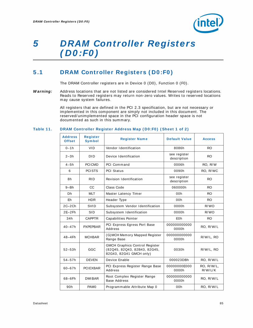
Datasheet 85
DRAM Controller Registers (D0:F0)
5 DRAM Controller Registers (D0:F0)
5.1 DRAM Controller Registers (D0:F0)
The DRAM Controller registers are in Device 0 (D0), Function 0 (F0).
Warning: Address locations that are not listed are considered Intel Reserved registers locations. Reads to Reserved registers may return non-zero values. Writes to reserved locations may cause system failures.
All registers that are defined in the PCI 2.3 specification, but are not necessary or implemented in this component are simply not included in this document. The reserved/unimplemented space in the PCI configuration header space is not documented as such in this summary.
Table 11. DRAM Controller Register Address Map (D0:F0) (Sheet 1 of 2)
Address Offset
Register Symbol
Register Name Default Value Access
0–1h VID Vendor Identification 8086h RO
2–3h DID Device Identificationsee register description
RO
4–5h PCICMD PCI Command 0006h RO, R/W
6 PCISTS PCI Status 0090h RO, R/WC
8h RID Revision Identificationsee register description
RO
9–Bh CC Class Code 060000h RO
Dh MLT Master Latency Timer 00h RO
Eh HDR Header Type 00h RO
2C–2Ch SVID Subsystem Vendor Identification 0000h R/WO
2E–2Fh SID Subsystem Identification 0000h R/WO
34h CAPPTR Capabilities Pointer E0h RO
40–47h PXPEPBARPCI Express Egress Port Base Address
0000000000000000h
RO, R/W/L
48–4Fh MCHBAR(G)MCH Memory Mapped Register Range Base
0000000000000000h
R/W/L, RO
52–53h GGCGMCH Graphics Control Register (82Q45, 82Q43, 82B43, 82G45, 82G43, 82G41 GMCH only)
0030h R/W/L, RO
54–57h DEVEN Device Enable 000023DBh RO, R/W/L
60–67h PCIEXBARPCI Express Register Range Base Address
00000000E0000000h
RO, R/W/L, R/W/L/K
68–6Fh DMIBARRoot Complex Register Range Base Address
0000000000000000h
RO, R/W/L
90h PAM0 Programmable Attribute Map 0 00h RO, R/W/L

DRAM Controller Registers (D0:F0)
86 Datasheet
91h PAM1 Programmable Attribute Map 1 00h RO, R/W/L
92h PAM2 Programmable Attribute Map 2 00h RO, R/W/L
93h PAM3 Programmable Attribute Map 3 00h RO, R/W/L
94h PAM4 Programmable Attribute Map 4 00h RO, R/W/L
95h PAM5 Programmable Attribute Map 5 00h RO, R/W/L
96h PAM6 Programmable Attribute Map 6 00h RO, R/W/L
97h LAC Legacy Access Control 00h R/W, R/W/L,
RO
98–99h REMAPBASE Remap Base Address Register 03FFh RO, R/W/L
9A–9Bh REMAPLIMIT Remap Limit Address Register 0000h RO, R/W/L
9Dh SMRAMSystem Management RAM Control
02h RO, R/W/L, R/
W, R/W/L/K
9Eh ESMRAMCExtended System Management RAM Control
38h R/W/L, R/WC,
RO
A0–A1h TOM Top of Memory 0001h RO, R/W/L
A2–A3h TOUUD Top of Upper Usable Dram 0000h R/W/L
A4–A7h GBSMGraphics Base of Stolen Memory (82Q45, 82Q43, 82B43, 82G45, 82G43, 82G41 GMCH only)
00000000h R/W/L, RO
A8–ABh BGSM Base of GTT stolen Memory 00000000h R/W/L, RO
AC–AFh TSEGMB TSEG Memory Base 00000000h RO, R/W/L
B0–B1h TOLUD Top of Low Usable DRAM 0010h R/W/L, RO
C8–C9h ERRSTS Error Status 0000h RO, R/WC/S
CA–CBh ERRCMD Error Command 0000h R/W, RO
CC–CDh SMICMD SMI Command 0000h RO, R/W
DC–DFh SKPD Scratchpad Data 00000000h R/W
E0–ECh CAPID0 Capability Identifier000000000000000000010C00
09h RO
Table 11. DRAM Controller Register Address Map (D0:F0) (Sheet 2 of 2)
Address Offset
Register Symbol
Register Name Default Value Access

Datasheet 87
DRAM Controller Registers (D0:F0)
5.1.1 VID—Vendor Identification
B/D/F/Type: 0/0/0/PCIAddress Offset: 0-1hDefault Value: 8086hAccess: ROSize: 16 bits
This register combined with the Device Identification register uniquely identifies any PCI device.
5.1.2 DID—Device Identification
B/D/F/Type: 0/0/0/PCIAddress Offset: 2-3hDefault Value: see table descriptionAccess: ROSize: 16 bits
This register combined with the Vendor Identification register uniquely identifies any PCI device.
Bit Access Default Value
RST/PWR
Description
15:0 RO 8086h CoreVendor Identification Number (VID): PCI standard identification for Intel.
Bit Access Default Value
RST/PWR
Description
15:0 ROsee
descriptionCore
Device Identification Number (DID): Identifier assigned to the (G)MCH core/primary PCI device. Refer to the Intel® 4 Series Chipset Family Specification Update for values in this register.

DRAM Controller Registers (D0:F0)
88 Datasheet
5.1.3 PCICMD—PCI Command
B/D/F/Type: 0/0/0/PCIAddress Offset: 4-5hDefault Value: 0006hAccess: RO, R/WSize: 16 bits
Since (G)MCH Device 0 does not physically reside on PCI_A many of the bits are not implemented.
Bit Access Default Value
RST/PWR
Description
15:10 RO 00h Core Reserved
9 RO 0b Core
Fast Back-to-Back Enable (FB2B): This bit controls whether or not the master can do fast back-to-back write. Since device 0 is strictly a target this bit is not implemented and is hardwired to 0. Writes to this bit position have no effect.
8 R/W 0b Core
SERR Enable (SERRE): This bit is a global enable bit for Device 0 SERR messaging. The (G)MCH does not have an SERR signal. The (G)MCH communicates the SERR condition by sending an SERR message over DMI to the ICH.1 = The (G)MCH is enabled to generate SERR messages
over DMI for specific Device 0 error conditions that are individually enabled in the ERRCMD and DMIUEMSK registers. The error status is reported in the ERRSTS, PCISTS, and DMIUEST registers.
0 = The SERR message is not generated by the (G)MCH for Device 0.
Note that this bit only controls SERR messaging for the Device 0. Device 1 has its own SERRE bits to control error reporting for error conditions occurring in that device. The control bits are used in a logical OR manner to enable the SERR DMI message mechanism.
7 RO 0b Core
Address/Data Stepping Enable (ADSTEP): Address/data stepping is not implemented in the (G)MCH, and this bit is hardwired to 0. Writes to this bit position have no effect.
6 R/W 0b Core
Parity Error Enable (PERRE): Controls whether or not the Master Data Parity Error bit in the PCI Status register can bet set.0 = Master Data Parity Error bit in PCI Status register can
NOT be set.1 = Master Data Parity Error bit in PCI Status register CAN
be set.
5 RO 0b CoreVGA Palette Snoop Enable (VGASNOOP): The (G)MCH does not implement this bit and it is hardwired to a 0.
4 RO 0b CoreMemory Write and Invalidate Enable (MWIE): The (G)MCH will never issue memory write and invalidate commands. This bit is therefore hardwired to 0.
3 RO 0b CoreSpecial Cycle Enable (SCE): The (G)MCH does not implement this bit and it is hardwired to a 0.

Datasheet 89
DRAM Controller Registers (D0:F0)
5.1.4 PCISTS—PCI Status
B/D/F/Type: 0/0/0/PCIAddress Offset: 6-7hDefault Value: 0090hAccess: RO, R/WCSize: 16 bits
This status register reports the occurrence of error events on Device 0's PCI interface. Since the (G)MCH Device 0 does not physically reside on PCI_A many of the bits are not implemented.
2 RO 1b CoreBus Master Enable (BME): The (G)MCH is always enabled as a master on the backbone. This bit is hardwired to a 1.
1 RO 1b CoreMemory Access Enable (MAE): The (G)MCH always allows access to main memory. This bit is not implemented and is hardwired to 1.
0 RO 0b CoreI/O Access Enable (IOAE): This bit is not implemented in the (G)MCH and is hardwired to a 0.
Bit Access Default Value
RST/PWR
Description
Bit Access Default Value
RST/PWR
Description
15 R/WC 0b CoreDetected Parity Error (DPE): This bit is set when this Device receives a Poisoned TLP.
14 R/WC 0b Core
Signaled System Error (SSE): This bit is set to 1 when the (G)MCH Device 0 generates an SERR message over DMI for any enabled Device 0 error condition. Device 0 error conditions are enabled in the PCICMD, ERRCMD, and DMIUEMSK registers. Device 0 error flags are read/reset from the PCISTS, ERRSTS, or DMIUEST registers. Software clears this bit by writing a 1 to it.
13 R/WC 0b Core
Received Master Abort Status (RMAS): This bit is set when the (G)MCH generates a DMI request that receives an Unsupported Request completion packet. Software clears this bit by writing a 1 to it.
12 R/WC 0b Core
Received Target Abort Status (RTAS): This bit is set when the (G)MCH generates a DMI request that receives a Completer Abort completion packet. Software clears this bit by writing a 1 to it.
11 RO 0b Core
Signaled Target Abort Status (STAS): The (G)MCH will not generate a Target Abort DMI completion packet or Special Cycle. This bit is not implemented in the (G)MCH and is hardwired to a 0. Writes to this bit position have no effect.
10:9 RO 00b Core
DEVSEL Timing (DEVT): These bits are hardwired to "00". Writes to these bit positions have no affect. Device 0 does not physically connect to PCI_A. These bits are set to "00" (fast decode) so that optimum DEVSEL timing for PCI_A is not limited by the (G)MCH.

DRAM Controller Registers (D0:F0)
90 Datasheet
5.1.5 RID—Revision Identification
B/D/F/Type: 0/0/0/PCIAddress Offset: 8hDefault Value: See description belowAccess: ROSize: 8 bits
This register contains the revision number of the (G)MCH Device 0. These bits are read only and writes to this register have no effect.
8 R/WC 0b Core
Master Data Parity Error Detected (DPD): This bit is set when DMI received a Poisoned completion from the ICH.This bit can only be set when the Parity Error Enable bit in the PCI Command register is set.
7 RO 1b Core
Fast Back-to-Back (FB2B): This bit is hardwired to 1. Writes to these bit positions have no effect. Device 0 does not physically connect to PCI_A. This bit is set to 1 (indicating fast back-to-back capability) so that the optimum setting for PCI_A is not limited by the (G)MCH.
6 RO 0b Core Reserved
5 RO 0b Core66 MHz Capable: Does not apply to PCI Express. Must be hardwired to 0.
4 RO 1b Core
Capability List (CLIST): This bit is hardwired to 1 to indicate to the configuration software that this device/function implements a list of new capabilities. A list of new capabilities is accessed via register CAPPTR at configuration address offset 34h. Register CAPPTR contains an offset pointing to the start address within configuration space of this device where the Capability Identification register resides.
3:0 RO 0000b Core Reserved
Bit Access Default Value
RST/PWR
Description
Bit Access Default Value
RST/PWR
Description
7:0 ROSee
descriptionCore
Revision Identification Number (RID): This is an 8-bit value that indicates the revision identification number for the (G)MCH Device 0. Refer to the Intel® 4 Series Chipset Family Specification Update for the value of this register.

Datasheet 91
DRAM Controller Registers (D0:F0)
5.1.6 CC—Class Code
B/D/F/Type: 0/0/0/PCIAddress Offset: 9-BhDefault Value: 060000hAccess: ROSize: 24 bits
This register identifies the basic function of the device, a more specific sub-class, and a register-specific programming interface.
5.1.7 MLT—Master Latency Timer
B/D/F/Type: 0/0/0/PCIAddress Offset: DhDefault Value: 00hAccess: ROSize: 8 bits
Device 0 in the (G)MCH is not a PCI master. Therefore, this register is not implemented.
Bit AccessDefault Value
RST/PWR Description
23:16 RO 06h CoreBase Class Code (BCC): This is an 8-bit value that indicates the base class code for the (G)MCH. 06h = Bridge device.
15:8 RO 00h Core
Sub-Class Code (SUBCC): This is an 8-bit value that indicates the category of Bridge into which the (G)MCH falls.00h = Host Bridge.
7:0 RO 00h Core
Programming Interface (PI): This is an 8-bit value that indicates the programming interface of this device. This value does not specify a particular register set layout and provides no practical use for this device.
Bit AccessDefault Value
RST/PWR Description
7:0 RO 00h Core Reserved

DRAM Controller Registers (D0:F0)
92 Datasheet
5.1.8 HDR—Header Type
B/D/F/Type: 0/0/0/PCIAddress Offset: EhDefault Value: 00hAccess: ROSize: 8 bits
This register identifies the header layout of the configuration space. No physical register exists at this location.
5.1.9 SVID—Subsystem Vendor Identification
B/D/F/Type: 0/0/0/PCIAddress Offset: 2C-2DhDefault Value: 0000hAccess: R/WOSize: 16 bits
This value is used to identify the vendor of the subsystem.
5.1.10 SID—Subsystem Identification
B/D/F/Type: 0/0/0/PCIAddress Offset: 2E-2FhDefault Value: 0000hAccess: R/WOSize: 16 bits
This value is used to identify a particular subsystem.
Bit Access Default Value
RST/PWR
Description
7:0 RO 00h Core
PCI Header (HDR): This field always returns 00h to indicate that the (G)MCH is a single function device with standard header layout. Reads and writes to this location have no effect.
Bit Access Default Value
RST/PWR
Description
15:0 R/WO 0000h Core
Subsystem Vendor ID (SUBVID): This field should be programmed during boot-up to indicate the vendor of the system board. After it has been written once, it becomes read only.
Bit Access Default Value
RST/PWR
Description
15:0 R/WO 0000h Core Subsystem ID (SUBID): This field should be programmed during BIOS initialization. After it has been written once, it becomes read only.

Datasheet 93
DRAM Controller Registers (D0:F0)
5.1.11 CAPPTR—Capabilities Pointer
B/D/F/Type: 0/0/0/PCIAddress Offset: 34hDefault Value: E0hAccess: ROSize: 8 bits
The CAPPTR provides the offset that is the pointer to the location of the first device capability in the capability list.
5.1.12 PXPEPBAR—PCI Express Egress Port Base Address
B/D/F/Type: 0/0/0/PCIAddress Offset: 40-47hDefault Value: 0000000000000000hAccess: RO, R/W/LSize: 64 bits
This is the base address for the PCI Express Egress Port MMIO Configuration space. There is no physical memory within this 4 KB window that can be addressed. The 4 KB reserved by this register does not alias to any PCI 2.3 compliant memory mapped space. On reset, the EGRESS port MMIO configuration space is disabled and must be enabled by writing a 1 to PXPEPBAREN [Dev 0, offset 40h, bit 0]
Note: All the bits in this register are locked in Intel TXT mode (82Q45/82Q43 GMCH only).
Bit Access Default Value
RST/PWR
Description
7:0 RO E0h Core
Capabilities Pointer (CAPPTR): This field is a pointer to the offset of the first capability ID register block. In this case the first capability is the product-specific Capability Identifier (CAPID0).
Bit Access Default Value
RST/PWR
Description
63:36 RO 0000000h Core Reserved
35:12 R/W/L 000000h Core
PCI Express Egress Port MMIO Base Address (PXPEPBAR): This field corresponds to bits 35:12 of the base address PCI Express Egress Port MMIO configuration space. BIOS will program this register resulting in a base address for a 4 KB block of contiguous memory address space. This register ensures that a naturally aligned 4 KB space is allocated within the first 6 4GB of addressable memory space. System Software uses this base address to program the (G)MCH MMIO register set.
11:1 RO 000h Core Reserved
0 R/W/L 0b Core
PXPEPBAR Enable (PXPEPBAREN): 0 = PXPEPBAR is disabled and does not claim any memory1 = PXPEPBAR memory mapped accesses are claimed and
decoded appropriately

DRAM Controller Registers (D0:F0)
94 Datasheet
5.1.13 MCHBAR—(G)MCH Memory Mapped Register Range Base
B/D/F/Type: 0/0/0/PCIAddress Offset: 48-4FhDefault Value: 0000000000000000hAccess: R/W/L, ROSize: 64 bits
This is the base address for the (G)MCH Memory Mapped Configuration space. There is no physical memory within this 16 KB window that can be addressed. The 16 KB reserved by this register does not alias to any PCI 2.3 compliant memory mapped space. On reset, the (G)MCH MMIO Memory Mapped Configuration space is disabled and must be enabled by writing a 1 to MCHBAREN [Device 0, offset48h, bit 0].
All the bits in this register are locked in Intel TXT mode (82Q45/82Q43 GMCH only).
Bit AccessDefault Value
RST/PWR Description
63:36 RO 0000000h Core Reserved
35:14 R/W/L 000000h Core
(G)MCH Memory Mapped Base Address (MCHBAR): This field corresponds to bits 35:14 of the base address (G)MCH Memory Mapped configuration space. BIOS will program this register resulting in a base address for a 16 KB block of contiguous memory address space. This register ensures that a naturally aligned 16 KB space is allocated within the first 64GB of addressable memory space. System Software uses this base address to program the (G)MCH Memory Mapped register set.
13:1 RO 0000h Core Reserved
0 R/W/L 0b Core
MCHBAR Enable (MCHBAREN):0 = MCHBAR is disabled and does not claim any memory1 = MCHBAR memory mapped accesses are claimed and
decoded appropriately

Datasheet 95
DRAM Controller Registers (D0:F0)
5.1.14 GGC—GMCH Graphics Control Register (Intel® 82Q45, 82Q43, 82B43, 82G45, 82G43, 82G41 GMCH Only)
B/D/F/Type: 0/0/0/PCIAddress Offset: 52-53hDefault Value: 0030hAccess: R/W/L, ROSize: 16 bits
Note: All the bits in this register are Intel TXT lockable (82Q45/82Q43 GMCH only).
Bit AccessDefault Value
RST/PWR
Description
15:12 RO 0h Core Reserved
11:8 R/W/L 0h Core
GTT Graphics Memory Size (GGMS): This field is used to select the amount of Main Memory that is pre-allocated to support the Internal Graphics Translation Table. The BIOS ensures that memory is pre-allocated only when Internal graphics is enabled.GSM is assumed to be a contiguous physical DRAM space with DSM, and BIOS needs to allocate a contiguous memory chunk. Hardware will drive the base of GSM from DSM only using the GSM size programmed in the register.0000 = No memory pre-allocated.0001 = No VT mode, 1 MB of memory pre-allocated for GTT.0011 = No VT mode, 2 MB of memory pre-allocated for GTT1001 = VT mode, 2 MB of memory pre-allocated for 1 MB of Global
GTT and 1 MB for Shadow GTT1010 = VT mode, 3 MB of memory pre-allocated for 1.5 MB of
Global GTT and 1.5 MB for Shadow GTT (82Q45 GMCH only)
1011 = VT mode, 4 MB of memory pre-allocated for 2 MB of Global GTT and 2 MB for Shadow GTT. (82Q45 GMCH only)
NOTE: All unspecified encodings of this register field are reserved, hardware functionality is not assured if used. This register is locked and becomes Read Only when the D_LCK bit in the SMRAM register is set.

DRAM Controller Registers (D0:F0)
96 Datasheet
7:4 R/W/L 0011b Core
Graphics Mode Select (GMS): This field is used to select the amount of Main Memory that is pre-allocated to support the Internal Graphics device in VGA (non-linear) and Native (linear) modes. The BIOS ensures that memory is pre-allocated only when Internal graphics is enabled.0000 = No memory pre-allocated. Device 2 (IGD) does not claim
VGA cycles (Memory and I/O), and the Sub-Class Code field within Device 2, Function 0 Class Code register is 80h.
0001 = Reserved0010 = Reserved0011 = Reserved0100 = Reserved0101 = DVMT (UMA) mode, 32 MB of memory pre-allocated for
frame buffer.0110 = DVMT (UMA) mode, 48 MB of memory pre-allocated for
frame buffer.0111 = DVMT (UMA) mode, 64 MB of memory pre-allocated for
frame buffer.1000 = DVMT (UMA) mode, 128 MB of memory pre-allocated for
frame buffer.1001 = DVMT (UMA) mode, 256 MB of memory pre-allocated for
frame buffer.1010 = DVMT (UMA) mode, 96 MB of memory pre-allocated (0 +
96).1011 = DVMT (UMA) mode, 160 MB of memory pre-allocated (64
+ 96).1100 = DVMT (UMA) mode, 224 MB of memory pre-allocated (128
+ 96).1101 = DVMT (UMA) mode, 352 MB of memory pre-allocated (256
+ 96).
NOTE: This register is locked and becomes Read Only when the D_LCK bit in the SMRAM register is set.
Hardware does not clear or set any of these bits automatically based on IGD being disabled/enabled.IOS Requirement: BIOS must not set this field to 000 if IVD (bit 1 of this register) is 0.
3:2 RO 00b Core Reserved
1 R/W/L 0b Core
IGD VGA Disable (IVD): 0 = Enable. Device 2 (IGD) claims VGA memory and IO cycles, the
Sub-Class Code within Device 2 Class Code register is 00h.1 = Disable. Device 2 (IGD) does not claim VGA cycles (Memory
and I/O), and the Sub- Class Code field within Device 2, Function 0 Class Code register is 80h.
BIOS Requirement: BIOS must not set this bit to 0 if the GMS field (bits 6:4 of this register) pre-allocates no memory. This bit MUST be set to 1 if Device 2 is disabled either via a fuse or fuse override (CAPID0[46] = 1) or via a register (DEVEN[3] = 0).This register is locked by Intel TXT (82Q45/82Q43 GMCH only) or ME stolen Memory lock.
0 RO 0b Core Reserved
Bit AccessDefault Value
RST/PWR
Description

Datasheet 97
DRAM Controller Registers (D0:F0)
5.1.15 DEVEN—Device Enable
B/D/F/Type: 0/0/0/PCIAddress Offset: 54-57hDefault Value: 000023DBhAccess: RO, R/W/LSize: 32 bits
Allows for enabling/disabling of PCI devices and functions that are within the (G)MCH. The table below the bit definitions describes the behavior of all combinations of transactions to devices controlled by this register.
Note: All the bits in this register are Intel TXT Lockable (82Q45/82Q43 GMCH only).
Bit AccessDefault Value
RST/PWR
Description
31:15 RO 00000h Core Reserved
14 R/W/L 0b Core Reserved
13 (82P45 MCH only)
R/W/L 1b CorePEG1 Enable (D6EN):0 = Bus 0, Device 6 is disabled and hidden.1 = Bus 0, Device 6 is enabled and visible.
13 (82Q45, 82Q43, 82B43, 82G45, 82G43, 82G41, 82P43 (G)MCH only)
R/W/L 1b Core Reserved
12:10 RO 000b Core Reserved
9 R/W/L 1b Core
EP Function 3 (D3F3EN):0 = Bus 0, Device 3, Function 3 is disabled and hidden1 = Bus 0, Device 3, Function 3 is enabled and visibleIf Device 3, Function 0 is disabled and hidden, then Device 3, Function 3 is also disabled and hidden independent of the state of this bit.If this (G)MCH does not have ME capability (CAPID0[57] = 1 or CAPID0[56] = 1), then Device 3, Function 3 is disabled and hidden independent of the state of this bit.
8 R/W/L 1b Core
EP Function 2 (D3F2EN):0 = Bus 0, Device 3, Function 2 is disabled and hidden1 = Bus 0, Device 3, Function 2 is enabled and visibleIf Device 3, Function 0 is disabled and hidden, then Device 3, Function 2 is also disabled and hidden independent of the state of this bit.If this (G)MCH does not have ME capability (CAPID0[57] = 1 or CAPID0[56] = 1) then Device 3 Function 2 is disabled and hidden independent of the state of this bit.
7 R/W/L 1b Core
EP Function 1 (D3F1EN):0 = Bus 0, Device 3, Function 1 is disabled and hidden1 = Bus 0, Device 3, Function 1 is enabled and visible.If Device 3, Function 0 is disabled and hidden, then Device 3, Function 1 is also disabled and hidden independent of the state of this bit.

DRAM Controller Registers (D0:F0)
98 Datasheet
6 R/W/L 1b CoreEP Function 0 (D3F0EN):0 = Bus 0, Device 3, Function 0 is disabled and hidden1 = Bus 0, Device 3, Function 0 is enabled and visible.
5 RO 0b Core Reserved
4(82Q45,
82Q43, 82B43, 82G45, 82G43, 82G41 GMCH
Only)
R/W/L 1b Core
Internal Graphics Engine Function 1 (D2F1EN):0 = Bus 0, Device 2, Function 1 is disabled and hidden1 = Bus 0, Device 2, Function 1 is enabled and visibleIf Device 2, Function 0 is disabled and hidden, then Device 2, Function 1 is also disabled and hidden independent of the state of this bit.If this component is not capable of Dual Independent Display (CAPID0[78] = 1), then this bit is hardwired to 0b to hide Device 2, Function 1.
4(82P45, 82P43
MCH Only)R/W/L 1b Core Reserved
3(82Q45,
82Q43, 82B43, 82G45, 82G43, 82G41 GMCH
Only)
R/W/L 1b Core
Internal Graphics Engine Function 0 (D2F0EN):0 = Bus 0, Device 2, Function 0 is disabled and hidden1 = Bus 0, Device 2, Function 0 is enabled and visibleIf this GMCH does not have internal graphics capability (CAPID0[46] = 1), then Device 2, Function 0 is disabled and hidden independent of the state of this bit.
3(82P45, 82P43
Only)R/W/L 1b Core Reserved
2 RO 0b Core Reserved
1 R/W/L 1b Core
PCI Express Port (D1EN):0 = Bus 0, Device 1, Function 0 is disabled and hidden. 1 = Bus 0, Device 1, Function 0 is enabled and visible.Default value is determined by the device capabilities (see CAPID0 [44]), SDVO Presence hardware strap and the sDVO/PCIe Concurrent hardware strap. Device 1 is Disabled on Reset if the SDVO Presence strap was sampled high, and the sDVO/PCIe Concurrent strap was sampled low at the last assertion of PWROK, and is enabled by default otherwise.
0 RO 1b CoreHost Bridge (D0EN): Bus 0, Device 0, Function 0 may not be disabled and is therefore hardwired to 1.
Bit AccessDefault Value
RST/PWR
Description

Datasheet 99
DRAM Controller Registers (D0:F0)
5.1.16 PCIEXBAR—PCI Express Register Range Base Address
B/D/F/Type: 0/0/0/PCIAddress Offset: 60-67hDefault Value: 00000000E0000000hAccess: RO, R/W/L, R/W/L/KSize: 64 bits
This is the base address for the PCI Express configuration space. This window of addresses contains the 4 KB of configuration space for each PCI Express device that can potentially be part of the PCI Express Hierarchy associated with the (G)MCH. There is not actual physical memory within this window of up to 256 MB that can be addressed. The actual length is determined by a field in this register. Each PCI Express Hierarchy requires a PCI Express BASE register. The (G)MCH supports one PCI Express hierarchy. The region reserved by this register does not alias to any PCI 2.3 compliant memory mapped space. For example MCHBAR reserves a 16 KB space and CHAPADR reserves a 4 KB space both outside of PCIEXBAR space. They cannot be overlayed on the space reserved by PCIEXBAR for devices 0 and 7 respectively.
On reset, this register is disabled and must be enabled by writing a 1 to the enable field in this register. This base address shall be assigned on a boundary consistent with the number of buses (defined by the Length field in this register), above TOLUD and still within 64 bit addressable memory space. All other bits not decoded are read only 0. The PCI Express Base Address cannot be less than the maximum address written to the Top of physical memory register (TOLUD). Software must ensure that these ranges do not overlap with known ranges located above TOLUD. Software must ensure that the sum of Length of enhanced configuration region + TOLUD + (other known ranges reserved above TOLUD) is not greater than the 64-bit addressable limit of 64 GB. In general system implementation and number of PCI/PCI express/PCI-X buses supported in the hierarchy will dictate the length of the region.
Note: All the bits in this register are locked in Intel TXT mode (82Q45/82Q43 GMCH only).
Bit AccessDefault Value
RST/PWR
Description
63:36 RO 0000000h Core Reserved
35:28 R/W/L 0Eh Core
PCI Express Base Address (PCIEXBAR): This field corresponds to bits 35:28 of the base address for PCI Express enhanced configuration space. BIOS will program this register resulting in a base address for a contiguous memory address space; size is defined by bits 2:1 of this register.This Base address shall be assigned on a boundary consistent with the number of buses (defined by the Length field in this register) above TOLUD and still within 64-bit addressable memory space. The address bits decoded depend on the length of the region defined by this register.The address used to access the PCI Express configuration space for a specific device can be determined as follows:
PCI Express Base Address + Bus Number * 1MB + Device Number * 32KB + Function Number * 4KB
The address used to access the PCI Express configuration space for Device 1 in this component is:
PCI Express Base Address + 0 * 1MB + 1 * 32KB + 0 * 4KB = PCI Express Base Address + 32KB.
Remember that this address is the beginning of the 4 KB space that contains both the PCI compatible configuration space and the PCI Express extended configuration space.

DRAM Controller Registers (D0:F0)
100 Datasheet
27 R/W/L 0b Core
128MB Base Address Mask (128ADMSK): This bit is either part of the PCI Express Base Address (R/W) or part of the Address Mask (RO, read 0b), depending on the value of bits 2:1 in this register.
26 R/W/L 0b Core
64MB Base Address Mask (64ADMSK): This bit is either part of the PCI Express Base Address (R/W) or part of the Address Mask (RO, read 0b), depending on the value of bits 2:1 in this register.
25:3 RO 000000h Core Reserved
2:1 R/W/L/K 00b Core
Length (LENGTH): This Field describes the length of this region. It provides the Enhanced Configuration Space Region/Buses Decoded00 =256 MB (buses 0–255). Bits 31:28 are decoded in the
PCI Express Base Address Field01 = 128 MB (Buses 0–127). Bits 31:27 are decoded in the
PCI Express Base Address Field.10 =64 MB (Buses 0–63). Bits 31:26 are decoded in the PCI
Express Base Address Field.11 =Reserved
0 R/W/L 0b Core
PCIEXBAR Enable (PCIEXBAREN):0 = The PCIEXBAR register is disabled. Memory read and
write transactions proceed as if there were no PCIEXBAR register. PCIEXBAR bits 35:26 are R/W with no functionality behind them.
1 = The PCIEXBAR register is enabled. Memory read and write transactions whose address bits 35:26 match PCIEXBAR will be translated to configuration reads and writes within the (G)MCH. These Translated cycles are routed as shown in the table above.
Bit AccessDefault Value
RST/PWR
Description

Datasheet 101
DRAM Controller Registers (D0:F0)
5.1.17 DMIBAR—Root Complex Register Range Base Address
B/D/F/Type: 0/0/0/PCIAddress Offset: 68-6FhDefault Value: 0000000000000000hAccess: RO, R/W/LSize: 64 bits
This is the base address for the Root Complex configuration space. This window of addresses contains the Root Complex Register set for the PCI Express Hierarchy associated with the (G)MCH. There is no physical memory within this 4 KB window that can be addressed. The 4 KB reserved by this register does not alias to any PCI 2.3 compliant memory mapped space. On reset, the Root Complex configuration space is disabled and must be enabled by writing a 1 to DMIBAREN [Dev 0, offset 68h, bit 0].
Note: All the bits in this register are locked in Intel TXT mode (82Q45/82Q43 GMCH only).
Bit AccessDefault Value
RST/PWR Description
63:36 RO 0000000h Core Reserved
35:12 R/W/L 000000h Core
DMI Base Address (DMIBAR): This field corresponds to bits 35:12 of the base address DMI configuration space. BIOS will program this register resulting in a base address for a 4 KB block of contiguous memory address space. This register ensures that a naturally aligned 4 KB space is allocated within the first 64 GB of addressable memory space. System Software uses this base address to program the DMI register set.
11:1 RO 000h Core Reserved
0 R/W/L 0b Core
DMIBAR Enable (DMIBAREN): 0 = DMIBAR is disabled and does not claim any memory1 = DMIBAR memory mapped accesses are claimed and
decoded appropriately

DRAM Controller Registers (D0:F0)
102 Datasheet
5.1.18 PAM0—Programmable Attribute Map 0
B/D/F/Type: 0/0/0/PCIAddress Offset: 90hDefault Value: 00hAccess: RO, R/W/LSize: 8 bits
This register controls the read, write, and shadowing attributes of the BIOS area from 0F0000h–0FFFFFh. The (G)MCH allows programmable memory attributes on 13 Legacy memory segments of various sizes in the 768 KB to 1 MB address range. Seven Programmable Attribute Map (PAM) Registers are used to support these features. Cacheability of these areas is controlled via the MTRR registers in the processor. Two bits are used to specify memory attributes for each memory segment. These bits apply to both host accesses and PCI initiator accesses to the PAM areas. These attributes are:
RE - Read Enable. When RE = 1, the processor read accesses to the corresponding memory segment are claimed by the (G)MCH and directed to main memory. Conversely, when RE = 0, the host read accesses are directed to PCI_A.
WE - Write Enable. When WE = 1, the host write accesses to the corresponding memory segment are claimed by the (G)MCH and directed to main memory. Conversely, when WE = 0, the host write accesses are directed to PCI_A.
The RE and WE attributes permit a memory segment to be Read Only, Write Only, Read/Write, or disabled. For example, if a memory segment has RE = 1 and WE = 0, the segment is Read Only. Each PAM Register controls two regions, typically 16 KB in size.
Note that the (G)MCH may hang if a PCI Express Graphics Attach or DMI originated access to Read Disabled or Write Disabled PAM segments occur (due to a possible IWB to non-DRAM).
For these reasons, the following critical restriction is placed on the programming of the PAM regions: At the time that a DMI or PCI Express Graphics Attach accesses to the PAM region may occur, the targeted PAM segment must be programmed to be both readable and writeable.
Note: All the bits in this register are locked in Intel TXT mode (82Q45/82Q43 GMCH only).
Bit AccessDefault Value
RST/PWR Description
7:6 RO 00b Core Reserved
5:4 R/W/L 00b Core
0F0000h-0FFFFFh Attribute (HIENABLE): This field controls the steering of read and write cycles that address the BIOS area from 0F0000h to 0FFFFFh.00 = DRAM Disabled: All accesses are directed to DMI.01 = Read Only: All reads are sent to DRAM. All writes are
forwarded to DMI.10 = Write Only: All writes are sent to DRAM. Reads are
serviced by DMI.11 = Normal DRAM Operation: All reads and writes are
serviced by DRAM.
3:0 RO 0h Core Reserved

Datasheet 103
DRAM Controller Registers (D0:F0)
5.1.19 PAM1—Programmable Attribute Map 1
B/D/F/Type: 0/0/0/PCIAddress Offset: 91hDefault Value: 00hAccess: RO, R/W/LSize: 8 bits
This register controls the read, write, and shadowing attributes of the BIOS areas from 0C0000h–0C7FFFh.
Note: All the bits in this register are locked in Intel TXT mode (82Q45/82Q43 GMCH only).
Bit AccessDefault Value
RST/PWR Description
7:6 RO 00b Core Reserved
5:4 R/W/L 00b Core
0C4000h-0C7FFFh Attribute (HIENABLE): This field controls the steering of read and write cycles that address the BIOS area from 0C4000h to 0C7FFFh.00 = DRAM Disabled: Accesses are directed to DMI.01 = Read Only: All reads are serviced by DRAM. All writes
are forwarded to DMI.10 = Write Only: All writes are sent to DRAM. Reads are
serviced by DMI.11 = Normal DRAM Operation: All reads and writes are
serviced by DRAM.
3:2 RO 00b Core Reserved
1:0 R/W/L 00b Core
0C0000h-0C3FFFh Attribute (LOENABLE): This field controls the steering of read and write cycles that address the BIOS area from 0C0000h to 0C3FFFh.00 = DRAM Disabled: Accesses are directed to DMI.01 = Read Only: All reads are serviced by DRAM. All
writes are forwarded to DMI.10 = Write Only: All writes are sent to DRAM. Reads are
serviced by DMI.11 = Normal DRAM Operation: All reads and writes are
serviced by DRAM.

DRAM Controller Registers (D0:F0)
104 Datasheet
5.1.20 PAM2—Programmable Attribute Map 2
B/D/F/Type: 0/0/0/PCIAddress Offset: 92hDefault Value: 00hAccess: RO, R/W/LSize: 8 bits
This register controls the read, write, and shadowing attributes of the BIOS areas from 0C8000h–0CFFFFh.
Note: All the bits in this register are locked in Intel TXT mode (82Q45/82Q43 GMCH only).
Bit Access Default Value
RST/PWR
Description
7:6 RO 00b Core Reserved
5:4 R/W/L 00b Core
0CC000h-0CFFFFh Attribute (HIENABLE): 00 = DRAM Disabled: Accesses are directed to DMI.01 = Read Only: All reads are serviced by DRAM. All
writes are forwarded to DMI.10 = Write Only: All writes are sent to DRAM. Reads are
serviced by DMI.11 = Normal DRAM Operation: All reads and writes are
serviced by DRAM.
3:2 RO 00b Core Reserved
1:0 R/W/L 00b Core
0C8000h-0CBFFFh Attribute (LOENABLE): This field controls the steering of read and write cycles that address the BIOS area from 0C8000h to 0CBFFFh.00 = DRAM Disabled: Accesses are directed to DMI.01 = Read Only: All reads are serviced by DRAM. All
writes are forwarded to DMI.10 = Write Only: All writes are sent to DRAM. Reads are
serviced by DMI.11 = Normal DRAM Operation: All reads and writes are
serviced by DRAM.

Datasheet 105
DRAM Controller Registers (D0:F0)
5.1.21 PAM3—Programmable Attribute Map 3
B/D/F/Type: 0/0/0/PCIAddress Offset: 93hDefault Value: 00hAccess: RO, R/W/LSize: 8 bits
This register controls the read, write, and shadowing attributes of the BIOS areas from 0D0000h–0D7FFFh.
Note: All the bits in this register are locked in Intel TXT mode (82Q45/82Q43 GMCH only).
Bit AccessDefault Value
RST/PWR Description
7:6 RO 00b Core Reserved
5:4 R/W/L 00b Core
0D4000h-0D7FFFh Attribute (HIENABLE): This field controls the steering of read and write cycles that address the BIOS area from 0D4000 to 0D7FFF.
00 = DRAM Disabled: Accesses are directed to DMI.01 = Read Only: All reads are serviced by DRAM. All writes
are forwarded to DMI.10 = Write Only: All writes are sent to DRAM. Reads are
serviced by DMI.11 = Normal DRAM Operation: All reads and writes are
serviced by DRAM.
3:2 RO 00b Core Reserved
1:0 R/W/L 00b Core
0D0000h-0D3FFFh Attribute (LOENABLE): This field controls the steering of read and write cycles that address the BIOS area from 0D0000h to 0D3FFFh.00 = DRAM Disabled: Accesses are directed to DMI.01 = Read Only: All reads are serviced by DRAM. All writes
are forwarded to DMI.10 = Write Only: All writes are sent to DRAM. Reads are
serviced by DMI.11 = Normal DRAM Operation: All reads and writes are
serviced by DRAM.

DRAM Controller Registers (D0:F0)
106 Datasheet
5.1.22 PAM4—Programmable Attribute Map 4
B/D/F/Type: 0/0/0/PCIAddress Offset: 94hDefault Value: 00hAccess: RO, R/W/LSize: 8 bits
This register controls the read, write, and shadowing attributes of the BIOS areas from 0D8000h–0DFFFFh.
Note: All the bits in this register are locked in Intel TXT mode (82Q45/82Q43 GMCH only).
Bit AccessDefault Value
RST/PWR Description
7:6 RO 00b Core Reserved
5:4 R/W/L 00b Core
0DC000h-0DFFFFh Attribute (HIENABLE): This field controls the steering of read and write cycles that address the BIOS area from 0DC000h to 0DFFFFh.00 = DRAM Disabled: Accesses are directed to DMI.01 = Read Only: All reads are serviced by DRAM. All
writes are forwarded to DMI.10 = Write Only: All writes are sent to DRAM. Reads are
serviced by DMI.11 = Normal DRAM Operation: All reads and writes are
serviced by DRAM.
3:2 RO 00b Core Reserved
1:0 R/W/L 00b Core
0D8000h-0DBFFFh Attribute (LOENABLE): This field controls the steering of read and write cycles that address the BIOS area from 0D8000h to 0DBFFFh.00 = DRAM Disabled: Accesses are directed to DMI.01 = Read Only: All reads are serviced by DRAM. All
writes are forwarded to DMI.10 = Write Only: All writes are sent to DRAM. Reads are
serviced by DMI.11 = Normal DRAM Operation: All reads and writes are
serviced by DRAM.
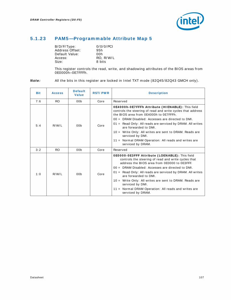
Datasheet 107
DRAM Controller Registers (D0:F0)
5.1.23 PAM5—Programmable Attribute Map 5
B/D/F/Type: 0/0/0/PCIAddress Offset: 95hDefault Value: 00hAccess: RO, R/W/LSize: 8 bits
This register controls the read, write, and shadowing attributes of the BIOS areas from 0E0000h–0E7FFFh.
Note: All the bits in this register are locked in Intel TXT mode (82Q45/82Q43 GMCH only).
Bit AccessDefault Value
RST/PWR Description
7:6 RO 00b Core Reserved
5:4 R/W/L 00b Core
0E4000h-0E7FFFh Attribute (HIENABLE): This field controls the steering of read and write cycles that address the BIOS area from 0E4000h to 0E7FFFh.00 = DRAM Disabled: Accesses are directed to DMI.01 = Read Only: All reads are serviced by DRAM. All writes
are forwarded to DMI.10 = Write Only: All writes are sent to DRAM. Reads are
serviced by DMI.11 = Normal DRAM Operation: All reads and writes are
serviced by DRAM.
3:2 RO 00b Core Reserved
1:0 R/W/L 00b Core
0E0000-0E3FFF Attribute (LOENABLE): This field controls the steering of read and write cycles that address the BIOS area from 0E0000 to 0E3FFF.
00 = DRAM Disabled: Accesses are directed to DMI.01 = Read Only: All reads are serviced by DRAM. All writes
are forwarded to DMI.10 = Write Only: All writes are sent to DRAM. Reads are
serviced by DMI.11 = Normal DRAM Operation: All reads and writes are
serviced by DRAM.

DRAM Controller Registers (D0:F0)
108 Datasheet
5.1.24 PAM6—Programmable Attribute Map 6
B/D/F/Type: 0/0/0/PCIAddress Offset: 96hDefault Value: 00hAccess: RO, R/W/LSize: 8 bits
This register controls the read, write, and shadowing attributes of the BIOS areas from 0E8000h–0EFFFFh.
Note: All the bits in this register are locked in Intel TXT mode (82Q45/82Q43 GMCH only).
Bit AccessDefault Value
RST/PWR Description
7:6 RO 00b Core Reserved
5:4 R/W/L 00b Core
0EC000h-0EFFFFh Attribute (HIENABLE): This field controls the steering of read and write cycles that address the BIOS area from 0E4000h to 0E7FFFh.00 = DRAM Disabled: Accesses are directed to DMI.01 = Read Only: All reads are serviced by DRAM. All
writes are forwarded to DMI.10 = Write Only: All writes are sent to DRAM. Reads are
serviced by DMI.11 = Normal DRAM Operation: All reads and writes are
serviced by DRAM.
3:2 RO 00b Core Reserved
1:0 R/W/L 00b Core
0E8000h-0EBFFFh Attribute (LOENABLE): This field controls the steering of read and write cycles that address the BIOS area from 0E0000h to 0E3FFFh.00 = DRAM Disabled: Accesses are directed to DMI.01 = Read Only: All reads are serviced by DRAM. All
writes are forwarded to DMI.10 = Write Only: All writes are sent to DRAM. Reads are
serviced by DMI.11 = Normal DRAM Operation: All reads and writes are
serviced by DRAM.

Datasheet 109
DRAM Controller Registers (D0:F0)
5.1.25 LAC—Legacy Access Control
B/D/F/Type: 0/0/0/PCIAddress Offset: 97hDefault Value: 00hAccess: R/W, R/W/L, ROSize: 8 bits
This 8-bit register controls a fixed DRAM hole from 15–16 MB.
Bit AccessDefault Value
RST/PWR
Description
7 R/W/L 0b Core
Hole Enable (HEN): This field enables a memory hole in DRAM space. The DRAM that lies "behind" this space is not remapped.0 = No memory hole.1 = Memory hole from 15 MB to 16 MB.This bit is Intel TXT lockable (82Q45/82Q43 GMCH only).
6:2 RO 00h Core Reserved
1(82P45 MCH
only)R/W 0b Core
PEG1 MDA Present (MDAP1): Definition of this bit is the same as for the adjacent PEG0 MDA Present bit except for all references to Device 1 are replaced with Device 6.
1(82Q45,
82Q43, 82B43, 82G45, 82G43, 82G41 GMCH and 82P43 MCH only)
R/W 0b Core Reserved

DRAM Controller Registers (D0:F0)
110 Datasheet
0 R/W 0b Core
PEG0 MDA Present (MDAP0): This bit works with the VGA Enable bits in the BCTRL register of Device 1 to control the routing of processor-initiated transactions targeting MDA compatible I/O and memory address ranges. This bit should not be set if device 1's VGA Enable bit is not set.If device 1's VGA enable bit is not set, then accesses to I/O address range x3BCh–x3BFh are forwarded to DMI.If the VGA enable bit is set and MDA is not present, then accesses to IO address range x3BCh–x3BFh are forwarded to PCI Express if the address is within the corresponding IOBASE and IOLIMIT, otherwise they are forwarded to DMI.MDA resources are defined as the following:Memory: 0B0000h–0B7FFFhI/O: 3B4h, 3B5h, 3B8h, 3B9h, 3BAh, 3BFh,
(including ISA address aliases, A[15:10] are not used in decode)
Any I/O reference that includes the I/O locations listed above, or their aliases, will be forwarded to the DMI even if the reference includes I/O locations not listed above.The following table shows the behavior for all combinations of MDA and VGA:VGAEN MDAP Description
0 0 All References to MDA and VGA space are routed to DMI
0 1 invalid combination1 0 All VGA and MDA references are
routed to PCI Express Graphics Attach.
1 1 All VGA references are routed to PCI Express Graphics Attach. MDA references are routed to DMI.
VGA and MDA memory cycles can only be routed across the PEG when MAE (PCICMD1[1]) is set. VGA and MDA I/O cycles can only be routed across the PEG if IOAE (PCICMD1[0]) is set.
Bit AccessDefault Value
RST/PWR
Description

Datasheet 111
DRAM Controller Registers (D0:F0)
5.1.26 REMAPBASE—Remap Base Address Register
B/D/F/Type: 0/0/0/PCIAddress Offset: 98-99hDefault Value: 03FFhAccess: RO, R/W/LSize: 16 bits
5.1.27 REMAPLIMIT—Remap Limit Address Register
B/D/F/Type: 0/0/0/PCIAddress Offset: 9A-9BhDefault Value: 0000hAccess: RO, R/W/LSize: 16 bits
Bit AccessDefault Value
RST/PWR Description
15:10 RO 000000b Core Reserved
9:0 R/W/L 3FFh Core
Remap Base Address [35:26] (REMAPBASE): The value in this register defines the lower boundary of the Remap window. The Remap window is inclusive of this address. In the decoder A[25:0] of the Remap Base Address are assumed to be 0s. Thus the bottom of the defined memory range will be aligned to a 64 MB boundary.When the value in this register is greater than the value programmed into the Remap Limit register, the Remap window is disabled.These bits are Intel TXT lockable (82Q45/82Q43 GMCH only) or ME stolen Memory lockable.
Bit AccessDefault Value
RST/PWR Description
15:10 RO 000000b Core Reserved
9:0 R/W/L 000h Core
Remap Limit Address [35:26] (REMAPLMT): The value in this register defines the upper boundary of the Remap window. The Remap window is inclusive of this address. In the decoder A[25:0] of the remap limit address are assumed to be Fh. Thus the top of the defined range will be one less than a 64 MB boundary.When the value in this register is less than the value programmed into the Remap Base register, the Remap window is disabled.These Bits are Intel TXT lockable (82Q45/82Q43 GMCH only) or ME stolen Memory lockable.

DRAM Controller Registers (D0:F0)
112 Datasheet
5.1.28 SMRAM—System Management RAM Control
B/D/F/Type: 0/0/0/PCIAddress Offset: 9DhDefault Value: 02hAccess: RO, R/W/L, R/W, R/W/L/KSize: 8 bits
The SMRAMC register controls how accesses to Compatible and Extended SMRAM spaces are treated. The Open, Close, and Lock bits function only when G_SMRAME bit is set to a 1. Also, the OPEN bit must be reset before the LOCK bit is set.
Bit AccessDefault Value
RST/PWR Description
7 RO 0b Core Reserved
6 R/W/L 0b Core
SMM Space Open (D_OPEN): When D_OPEN=1 and D_LCK=0, the SMM space DRAM is made visible even when SMM decode is not active. This is intended to help BIOS initialize SMM space. Software should ensure that D_OPEN=1 and D_CLS=1 are not set at the same time.
5 R/W 0b Core
SMM Space Closed (D_CLS): When D_CLS = 1 SMM space DRAM is not accessible to data references, even if SMM decode is active. Code references may still access SMM space DRAM. This will allow SMM software to reference through SMM space to update the display even when SMM is mapped over the VGA range. Software should ensure that D_OPEN=1 and D_CLS=1 are not set at the same time.
4 R/W/L/K 0b Core
SMM Space Locked (D_LCK): When D_LCK is set to 1 then D_OPEN is reset to 0 and D_LCK, D_OPEN, C_BASE_SEG, H_SMRAM_EN, TSEG_SZ and TSEG_EN become read only. D_LCK can be set to 1 via a normal configuration space write but can only be cleared by a Full Reset. The combination of D_LCK and D_OPEN provide convenience with security. The BIOS can use the D_OPEN function to initialize SMM space and then use D_LCK to "lock down" SMM space in the future so that no application software (or BIOS itself) can violate the integrity of SMM space, even if the program has knowledge of the D_OPEN function.
3 R/W/L 0b Core
Global SMRAM Enable (G_SMRAME): If set to a 1, then Compatible SMRAM functions are enabled, providing 128 KB of DRAM accessible at the A0000h address while in SMM (ADSB with SMM decode). To enable Extended SMRAM function this bit has be set to 1. Refer to the section on SMM for more details. Once D_LCK is set, this bit becomes read only.
2:0 RO 010b Core
Compatible SMM Space Base Segment (C_BASE_SEG): This field indicates the location of SMM space. SMM DRAM is not remapped. It is simply made visible if the conditions are right to access SMM space, otherwise the access is forwarded to DMI. Since the (G)MCH supports only the SMM space between A0000h and BFFFFh, this field is hardwired to 010b.

Datasheet 113
DRAM Controller Registers (D0:F0)
5.1.29 ESMRAMC—Extended System Management RAM Control
B/D/F/Type: 0/0/0/PCIAddress Offset: 9EhDefault Value: 38hAccess: R/W/L, R/WC, ROSize: 8 bits
The Extended SMRAM register controls the configuration of Extended SMRAM space. The Extended SMRAM (E_SMRAM) memory provides a write-back cacheable SMRAM memory space that is above 1 MB.
Bit AccessDefault Value
RST/PWR Description
7 R/W/L 0b Core
Enable High SMRAM (H_SMRAME): Controls the SMM memory space location (i.e., above 1 MB or below 1 MB) When G_SMRAME is 1 and H_SMRAME is set to 1, the high SMRAM memory space is enabled. SMRAM accesses within the range 0FEDA0000h to 0FEDBFFFFh are remapped to DRAM addresses within the range 000A0000h to 000BFFFFh. Once D_LCK has been set, this bit becomes read only.
6 R/WC 0b Core
Invalid SMRAM Access (E_SMERR): This bit is set when the processor has accessed the defined memory ranges in Extended SMRAM (High Memory and T-segment) while not in SMM space and with the D-OPEN bit = 0. It is software's responsibility to clear this bit. The software must write a 1 to this bit to clear it.
5 RO 1b CoreSMRAM Cacheable (SM_CACHE): This bit is forced to 1 by the (G)MCH.
4 RO 1b CoreL1 Cache Enable for SMRAM (SM_L1): This bit is forced to 1 by the (G)MCH.
3 RO 1b Core L2 Cache Enable for SMRAM (SM_L2): This bit is forced to 1 by the (G)MCH.

DRAM Controller Registers (D0:F0)
114 Datasheet
5.1.30 TOM—Top of Memory
B/D/F/Type: 0/0/0/PCIAddress Offset: A0-A1hDefault Value: 0001hAccess: RO, R/W/LSize: 16 bits
This Register contains the size of physical memory. BIOS determines the memory size reported to the OS using this Register.
Note: All the bits in this register are locked in Intel TXT mode (82Q45/82Q43 GMCH only).
2:1 R/W/L 00b Core
TSEG Size (TSEG_SZ): Selects the size of the TSEG memory block if enabled. Memory from the top of DRAM space is partitioned away so that it may only be accessed by the processor interface and only then when the SMM bit is set in the request packet. Non-SMM accesses to this memory region are sent to DMI when the TSEG memory block is enabled.00 = 1 MB TSEG. (TOLUD – GTT Graphics Memory Size –
Graphics Stolen Memory Size – 1M) to (TOLUD – GTT Graphics Memory Size – Graphics Stolen Memory Size).
01 = 2 MB TSEG (TOLUD – GTT Graphics Memory Size – Graphics Stolen Memory Size – 2M) to (TOLUD – GTT Graphics Memory Size – Graphics Stolen Memory Size).
10 = 8 MB TSEG (TOLUD – GTT Graphics Memory Size – Graphics Stolen Memory Size – 8M) to (TOLUD – GTT Graphics Memory Size – Graphics Stolen Memory Size).
11 = Reserved.Once D_LCK has been set, these bits becomes read only.
0 R/W/L 0b Core
TSEG Enable (T_EN): Enabling of SMRAM memory for Extended SMRAM space only. When G_SMRAME = 1 and TSEG_EN = 1, the TSEG is enabled to appear in the appropriate physical address space. Note that once D_LCK is set, this bit becomes read only.
Bit AccessDefault Value
RST/PWR Description
Bit AccessDefault Value
RST/PWR Description
15:10 RO 00h Core Reserved
9:0 R/W/L 001h Core
Top of Memory (TOM): This register reflects the total amount of populated physical memory. This is NOT necessarily the highest main memory address (holes may exist in main memory address map due to addresses allocated for memory-mapped I/O). These bits correspond to address bits 35:26 (64 MB granularity). Bits 25:0 are assumed to be 0. The (G)MCH determines the base of EP stolen memory by subtracting the EP stolen memory size from TOM.

Datasheet 115
DRAM Controller Registers (D0:F0)
5.1.31 TOUUD—Top of Upper Usable DRAMB/D/F/Type: 0/0/0/PCIAddress Offset: A2-A3hDefault Value: 0000hAccess: R/W/LSize: 16 bits
This 16 bit register defines the Top of Upper Usable DRAM.
Configuration software must set this value to TOM minus all EP stolen memory if reclaim is disabled. If reclaim is enabled, this value must be set to reclaim limit + 1byte 64 MB aligned since reclaim limit is 64M B aligned. Address bits 19:0 are assumed to be 000_0000h for the purposes of address comparison. The Host interface positively decodes an address towards DRAM if the incoming address is less than the value programmed in this register and greater than or equal to 4 B.
Note: All the bits in this register are locked in Intel TXT mode (82Q45/82Q43 GMCH only).
Bit AccessDefault Value
RST/PWR Description
15:0 R/W/L 0000h Core
TOUUD (TOUUD): This register contains bits 35:20 of an address one byte above the maximum DRAM memory above 4 GB that is usable by the operating system. Configuration software must set this value to TOM minus all EP stolen memory, if reclaim is disabled. If reclaim is enabled, this value must be set to reclaim limit 64 MB aligned since reclaim limit + 1byte is 64 MB aligned. Address bits 19:0 are assumed to be 000_0000h for the purposes of address comparison. The Host interface positively decodes an address towards DRAM if the incoming address is less than the value programmed in this register and greater than 4 GB.

DRAM Controller Registers (D0:F0)
116 Datasheet
5.1.32 GBSM—Graphics Base of Stolen Memory (Intel® 82Q45, 82Q43, 82B43, 82G45, 82G43, 82G41 GMCH Only)B/D/F/Type: 0/0/0/PCIAddress Offset: A4-A7hDefault Value: 00000000hAccess: R/W/L, ROSize: 32 bits
This register contains the base address of graphics data stolen DRAM memory. BIOS determines the base of graphics data stolen memory by subtracting the graphics data stolen memory size (PCI Device 0, offset 52h, bits 6:4) from TOLUD (PCI Device 0, offset B0h, bits 15:4).
Note: This register is locked and becomes Read Only when the D_LCK bit in the SMRAM register is set.
5.1.33 BGSM—Base of GTT stolen Memory (Intel® 82Q45, 82Q43, 82B43, 82G45, 82G43, 82G41 GMCH Only)
B/D/F/Type: 0/0/0/PCIAddress Offset: A8-ABhDefault Value: 00000000hAccess: R/W/L, ROSize: 32 bits
This register contains the base address of stolen DRAM memory for the GTT. BIOS determines the base of GTT stolen memory by subtracting the GTT graphics stolen memory size (PCI Device 0, offset 52h, bits 9:8) from the graphics stolen memory base (PCI Device 0, offset A4h, bits 31:20).
Note: This register is locked and becomes Read Only when the D_LCK bit in the SMRAM register is set.
Bit AccessDefault Value
RST/PWR Description
31:20 R/W/L 000h Core
Graphics Base of Stolen Memory (GBSM): This register contains bits 31:20 of the base address of stolen DRAM memory. BIOS determines the base of graphics stolen memory by subtracting the graphics stolen memory size (PCI Device 0, offset 52h, bits 6:4) from TOLUD (PCI Device 0, offset B0h, bits 15:4).
NOTE: This register is locked and becomes Read Only when the D_LCK bit in the SMRAM register is set.
19:0 RO 00000h Core Reserved
Bit AccessDefault Value
RST/PWR Description
31:20 R/W/L 000h Core
Graphics Base of Stolen Memory (GBSM): This register contains bits 31:20 of the base address of stolen DRAM memory. BIOS determines the base of graphics stolen memory by subtracting the graphics stolen memory size (PCI Device 0, offset 52h, bits 9:8) from the graphics stolen memory base (PCI Device 0, offset A4h, bits 31:20).
NOTE: This register is locked and becomes Read Only when the D_LCK bit in the SMRAM register is set.
19:0 RO 00000h Core Reserved

Datasheet 117
DRAM Controller Registers (D0:F0)
5.1.34 TSEGMB—TSEG Memory Base
B/D/F/Type: 0/0/0/PCIAddress Offset: AC-AFhDefault Value: 00000000hAccess: RO, R/W/LSize: 32 bits
This register contains the base address of TSEG DRAM memory. BIOS determines the base of TSEG memory by subtracting the TSEG size (PCI Device 0, offset 9Eh, bits 2:1) from graphics GTT stolen base (PCI Device 0, offset A8h, bits 31:20).
Once D_LCK has been set, these bits becomes read only.
5.1.35 TOLUD—Top of Low Usable DRAMB/D/F/Type: 0/0/0/PCIAddress Offset: B0-B1hDefault Value: 0010hAccess: R/W/L, ROSize: 16 bits
This 16 bit register defines the Top of Low Usable DRAM. TSEG, GTT Graphics memory and Graphics Stolen Memory are within the DRAM space defined. From the top, (G)MCH optionally claims 1 to 64 MB of DRAM for internal graphics if enabled, 1, 2 MB of DRAM for GTT Graphics Stolen Memory (if enabled) and 1, 2, or 8 MB of DRAM for TSEG if enabled.
Programming Example:
C1DRB3 is set to 4 GB
TSEG is enabled and TSEG size is set to 1 MB
Internal Graphics is enabled, and Graphics Mode Select is set to 32 MB
GTT Graphics Stolen Memory Size set to 2 MB
BIOS knows the operating system requires 1 GB of PCI space.
BIOS also knows the range from FEC0_0000h to FFFF_FFFFh is not usable by the system. This 20 MB range at the very top of addressable memory space is lost to APIC and Intel TXT (82Q45/82Q43 GMCH only).
According to the above equation, TOLUD is originally calculated to: 4 GB = 1_0000_0000h
The system memory requirements are: 4 GB (max addressable space) – 1 GB (PCI space) – 35 MB (lost memory) = 3 GB – 35 MB (minimum granularity) = ECB0_0000h.
Bit AccessDefault Value
RST/PWR Description
31:20 R/W/L 000h Core
TESG Memory base (TSEGMB): This register contains bits 31:20 of the base address of TSEG DRAM memory. BIOS determines the base of TSEG memory by subtracting the TSEG size (PCI Device 0, offset 9Eh, bits 2:1) from graphics GTT stolen base (PCI Device 0, offset A8h, bits 31:20).Once D_LCK has been set, these bits becomes read only.
19:0 RO 00000h Core Reserved

DRAM Controller Registers (D0:F0)
118 Datasheet
Since ECB0_0000h (PCI and other system requirements) is less than 1_0000_0000h, TOLUD should be programmed to ECBh.
Note: All the bits in this register are locked in Intel TXT mode (82Q45/82Q43 GMCH only).
5.1.36 ERRSTS—Error Status
B/D/F/Type: 0/0/0/PCIAddress Offset: C8-C9hDefault Value: 0000hAccess: RO, R/WC/SSize: 16 bits
This register is used to report various error conditions via the SERR DMI messaging mechanism. An SERR DMI message is generated on a zero to one transition of any of these flags (if enabled by the ERRCMD and PCICMD registers).
These bits are set regardless of whether or not the SERR is enabled and generated. After the error processing is complete, the error logging mechanism can be unlocked by clearing the appropriate status bit by software writing a 1 to it.
Bit AccessDefault Value
RST/PWR
Description
15:4 R/W/L 001h Core
Top of Low Usable DRAM (TOLUD): This register contains bits 31:20 of an address one byte above the maximum DRAM memory below 4 GB that is usable by the operating system. Address bits 31:20 programmed to 01h implies a minimum memory size of 1 MB. Configuration software must set this value to the smaller of the following 2 choices: maximum amount memory in the system minus ME stolen memory plus one byte or the minimum address allocated for PCI memory. Address bits 19:0 are assumed to be 0_0000h for the purposes of address comparison. The Host interface positively decodes an address towards DRAM if the incoming address is less than the value programmed in this register.Note that the Top of Low Usable DRAM is the lowest address above both Graphics Stolen memory and TSEG. BIOS determines the base of Graphics Stolen Memory by subtracting the Graphics Stolen Memory Size from TOLUD and further decrements by TSEG size to determine base of TSEG. This register must be 64 MB aligned when reclaim is enabled.
3:0 RO 0000b Core Reserved

Datasheet 119
DRAM Controller Registers (D0:F0)
Bit AccessDefault Value
RST/PWR Description
15:13 RO 000b Core Reserved
12 R/WC/S 0b Core(G)MCH Software Generated Event for SMI (GSGESMI): This indicates the source of the SMI was a Device 2 Software Event.
11 R/WC/S 0b Core
(G)MCH Thermal Sensor Event for SMI/SCI/SERR (GTSE): This bit indicates that a (G)MCH Thermal Sensor trip has occurred and an SMI, SCI, or SERR has been generated. The status bit is set only if a message is sent based on Thermal event enables in Error command, SMI command and SCI command registers. A trip point can generate one of SMI, SCI, or SERR interrupts (two or more per event is invalid). Multiple trip points can generate the same interrupt, if software chooses this mode, subsequent trips may be lost. If this bit is already set, then an interrupt message will not be sent on a new thermal sensor event.
10 RO 0b Core Reserved
9 R/WC/S 0b CoreLOCK to non-DRAM Memory Flag (LCKF): When this bit is set to 1, the (G)MCH has detected a lock operation to memory space that did not map into DRAM.
8 RO 0b Core Received Refresh Timeout Flag (RRTOF): Reserved
7 R/WC/S 0b Core
DRAM Throttle Flag (DTF):1 = Indicates that a DRAM Throttling condition occurred.0 = Software has cleared this flag since the most recent
throttling event.
6:2 RO 00h Core Reserved
1 R/WC/S 0b Core
Multiple-bit DRAM ECC Error Flag (DMERR): If this bit is set to 1, a memory read data transfer had an uncorrectable multiple-bit error. When this bit is set the address, channel number, and device number that caused the error are logged in the DEAP register. Once this bit is set, the DEAP, DERRSYN, and DERRDST fields are locked until the processor clears this bit by writing a 1. Software uses bits [1:0] to detect whether the logged error address is for Single or Multiple-bit error. This bit is reset on PWROK.
0 R/WC/S 0b Core
Single-bit DRAM ECC Error Flag (DSERR): If this bit is set to 1, a memory read data transfer had a single-bit correctable error and the corrected data was sent for the access. When this bit is set, the address and device number that caused the error are logged in the DEAP register. Once this bit is set, the DEAP, DERRSYN, and DERRDST fields are locked to further single bit error updates until the processor clears this bit by writing a 1. A multiple bit error that occurs after this bit is set will overwrite the DEAP and DERRSYN fields with the multiple-bit error signature and the DMERR bit will also be set. A single bit error that occurs after a multi-bit error will set this bit but will not overwrite the other fields. This bit is reset on PWROK.

DRAM Controller Registers (D0:F0)
120 Datasheet
5.1.37 ERRCMD—Error CommandB/D/F/Type: 0/0/0/PCIAddress Offset: CA-CBhDefault Value: 0000hAccess: R/W, ROSize: 16 bits
This register controls the (G)MCH responses to various system errors. Since the (G)MCH does not have an SERRB signal, SERR messages are passed from the (G)MCH to the ICH over DMI.
When a bit in this register is set, a SERR message will be generated on DMI whenever the corresponding flag is set in the ERRSTS register. The actual generation of the SERR message is globally enabled for Device 0 via the PCI Command register.
Bit AccessDefault Value
RST/PWR
Description
15:12 RO 0h Core Reserved
11 R/W 0b Core
SERR on (G)MCH Thermal Sensor Event (TSESERR):1 = The (G)MCH generates a DMI SERR special cycle when bit 11 of
the ERRSTS is set. The SERR must not be enabled at the same time as the SMI for the same thermal sensor event.
0 = Reporting of this condition via SERR messaging is disabled.
10 RO 0b Core Reserved
9 R/W 0b Core
SERR on LOCK to non-DRAM Memory (LCKERR):1 = The (G)MCH will generate a DMI SERR special cycle whenever a
processor lock cycle is detected that does not hit DRAM.0 = Reporting of this condition via SERR messaging is disabled.
8 R/W 0b Core
SERR on DRAM Refresh Timeout (DRTOERR):1 = The (G)MCH generates a DMI SERR special cycle when a DRAM
Refresh timeout occurs.0 = Reporting of this condition via SERR messaging is disabled.
7 R/W 0b Core
SERR on DRAM Throttle Condition (DTCERR):1 = The (G)MCH generates a DMI SERR special cycle when a DRAM
Read or Write Throttle condition occurs.0 = Reporting of this condition via SERR messaging is disabled.
6:2 RO 00h Core Reserved
1 R/W 0b Core
SERR Multiple-Bit DRAM ECC Error (DMERR):1 = The (G)MCH generates a SERR message over DMI when it
detects a multiple-bit error reported by the DRAM controller.0 = Reporting of this condition via SERR messaging is disabled. For
systems not supporting ECC, this bit must be disabled.
0 R/W 0b Core
SERR on Single-bit ECC Error (DSERR):1 = The (G)MCH generates a SERR special cycle over DMI when the
DRAM controller detects a single bit error.0 = Reporting of this condition via SERR messaging is disabled.For systems that do not support ECC, this bit must be disabled.

Datasheet 121
DRAM Controller Registers (D0:F0)
5.1.38 SMICMD—SMI Command
B/D/F/Type: 0/0/0/PCIAddress Offset: CC-CDhDefault Value: 0000hAccess: RO, R/WSize: 16 bits
This register enables various errors to generate an SMI DMI special cycle. When an error flag is set in the ERRSTS register, it can generate an SERR, SMI, or SCI DMI special cycle when enabled in the ERRCMD, SMICMD, or SCICMD registers, respectively. Note that one and only one message type can be enabled.
Bit AccessDefault Value
RST/PWR Description
15:12 RO 0h Core Reserved
11 R/W 0b Core
SMI on (G)MCH Thermal Sensor Trip (TSTSMI):1 = A SMI DMI special cycle is generated by (G)MCH when
the thermal sensor trip requires an SMI. A thermal sensor trip point cannot generate more than one special cycle.
0 = Reporting of this condition via SMI messaging is disabled.
10:2 RO 000h Core Reserved
1 R/W 0b Core
SMI on Multiple-Bit DRAM ECC Error (DMESMI):1 = The (G)MCH generates an SMI DMI message when it
detects a multiple-bit error reported by the DRAM controller.
0 = Reporting of this condition via SMI messaging is disabled. For systems not supporting ECC this bit must be disabled.
0 R/W 0b Core
SMI on Single-bit ECC Error (DSESMI):1 = The (G)MCH generates an SMI DMI special cycle when
the DRAM controller detects a single bit error.0 = Reporting of this condition via SMI messaging is
disabled. For systems that do not support ECC this bit must be disabled.

DRAM Controller Registers (D0:F0)
122 Datasheet
5.1.39 SKPD—Scratchpad Data
B/D/F/Type: 0/0/0/PCIAddress Offset: DC-DFhDefault Value: 00000000hAccess: R/WSize: 32 bits
This register holds 32 writable bits with no functionality behind them. It is for the convenience of BIOS and graphics drivers.
5.1.40 CAPID0—Capability Identifier
B/D/F/Type: 0/0/0/PCIAddress Offset: E0-EChDefault Value: 000000000000000000010C0009hAccess: ROSize: 104 bitsBIOS Optimal Default 0h
Bit AccessDefault Value
RST/PWR Description
31:0 R/W 00000000h Core Scratchpad Data (SKPD): 1 DWord of data storage.
Bit AccessDefault Value
RST/PWR Description
103:28 RO 0000b Core Reserved
27:24 RO 1h CoreCAPID Version (CAPIDV): This field has the value 0001b to identify the first revision of the CAPID register definition.
23:16 RO 0Ch CoreCAPID Length (CAPIDL): This field has the value 0Ch to indicate the structure length (12 bytes).
15:8 RO 00h CoreNext Capability Pointer (NCP): This field is hardwired to 00h indicating the end of the capabilities linked list.
7:0 RO 09h CoreCapability Identifier (CAP_ID): This field has the value 1001b to identify the CAP_ID assigned by the PCI SIG for vendor dependent capability pointers.

Datasheet 123
DRAM Controller Registers (D0:F0)
5.2 MCHBAR
Address Offset
Register Symbol
Register NameDefault Value
Access
111h CHDECMISC Channel Decode Miscellaneous 00h R/W/L, R/W
200–201h C0DRB0 Channel 0 DRAM Rank Boundary Address 0 0000h R/W/L, RO
202–203h C0DRB1 Channel 0 DRAM Rank Boundary Address 1 0000h RO, R/W/L
204–205h C0DRB2 Channel 0 DRAM Rank Boundary Address 2 0000h RO, R/W/L
206–207h C0DRB3 Channel 0 DRAM Rank Boundary Address 3 0000h R/W, RO
208–209h C0DRA01 Channel 0 DRAM Rank 0,1 Attribute 0000h R/W/L
20A–20Bh C0DRA23 Channel 0 DRAM Rank 2,3 Attribute 0000h R/W/L
250–251h C0CYCTRKPCHG Channel 0 CYCTRK PCHG 0000h R/W, RO
252–255h C0CYCTRKACT Channel 0 CYCTRK ACT 00000000h R/W, RO
256–257h C0CYCTRKWR Channel 0 CYCTRK WR 0000h R/W
258–25Ah C0CYCTRKRD Channel 0 CYCTRK READ 000000h R/W, RO
25B–25Ch C0CYCTRKREFR Channel 0 CYCTRK REFR 0000h RO, R/W
260–263h C0CKECTRL Channel 0 CKE Control 00000800h R/W, RO
269–26Eh C0REFRCTRL Channel 0 DRAM Refresh Control 241830000C30h
R/W, RO
29C–29Fh C0ODTCTRL Channel 0 ODT Control 00000000h RO, R/W
602–603h C1DRB1 Channel 1 DRAM Rank Boundary Address 1 0000h R/W/L, RO
604–605h C1DRB2 Channel 1 DRAM Rank Boundary Address 2 0000h R/W/L, RO
606–607h C1DRB3 Channel 1 DRAM Rank Boundary Address 3 0000h R/W, RO
608–609h C1DRA01 Channel 1 DRAM Rank 0,1 Attributes 0000h R/W/L
60A–60Bh C1DRA23 Channel 1 DRAM Rank 2,3 Attributes 0000h R/W/L
650–651h C1CYCTRKPCHG Channel 1 CYCTRK PCHG 0000h R/W, RO
652–655h C1CYCTRKACT Channel 1 CYCTRK ACT 00000000h R/W, RO
656–657h C1CYCTRKWR Channel 1 CYCTRK WR 0000h R/W
658–65Ah C1CYCTRKRD Channel 1 CYCTRK READ 000000h R/W, RO
660–663h C1CKECTRL Channel 1 CKE Control 00000800h R/W, RO
669–66Eh C1REFRCTRL Channel 1 DRAM Refresh Control 241830000C30h
R/W, RO
69C–69Fh C1ODTCTRL Channel 1 ODT Control 00000000h R/W, RO
A00–A01h EPC0DRB0 EP Channel 0 DRAM Rank Boundary Address 0 0000h R/W, RO
A02–A03h EPC0DRB1 EP Channel 0 DRAM Rank Boundary Address 1 0000h RO, R/W
A04–A05h EPC0DRB2 EP Channel 0 DRAM Rank Boundary Address 2 0000h RO, R/W
A06–A07h EPC0DRB3 EP Channel 0 DRAM Rank Boundary Address 3 0000h R/W, RO

DRAM Controller Registers (D0:F0)
124 Datasheet
A08–A09h EPC0DRA01 EP Channel 0 DRAM Rank 0,1 Attribute 0000h R/W
A0A–A0Bh EPC0DRA23 EP Channel 0 DRAM Rank 2,3 Attribute 0000h R/W
A19–A1AhEPDCYCTRKWR
TPREEPD CYCTRK WRT PRE 0000h R/W, RO
A1C–A1FhEPDCYCTRKWR
TACTEPD CYCTRK WRT ACT 00000000h RO, R/W
A20–A21hEPDCYCTRKWR
TWREPD CYCTRK WRT WR 0000h R/W, RO
A22–A23hEPDCYCTRKWR
TREFEPD CYCTRK WRT REF 0000h RO, R/W
A24–A26hEPDCYCTRKWR
TRDEPD CYCTRK WRT READ 000000h R/W
A28–A2ChEPDCKECONFIG
REGEPD CKE related configuration registers 00E0000000
hR/W
A30–A33h EPDREFCONFIG EP DRAM Refresh Configuration 40000C30h RO, R/W
CD8h TSC1 Thermal Sensor Control 1 00hR/W/L, R/W,
RS/WC
CD9h TSC2 Thermal Sensor Control 2 00h R/W/L, RO
CDAh TSS Thermal Sensor Status 00h RO
CDC–CDFh TSTTP Thermal Sensor Temperature Trip Point 00000000hRO, R/W, R/W/L
CE2h TCO Thermal Calibration Offset 00hR/W/L/K,
R/W/L
CE4h THERM1 Hardware Throttle Control 00hRO, R/W/L,
R/W/L/K
CEA–CEBh TIS Thermal Interrupt Status 0000h R/WC, RO
CF1h TSMICMD Thermal SMI Command 00h RO, R/W
F14–F17h PMSTS Power Management Status 00000000h R/WC/S, RO
Address Offset
Register Symbol
Register NameDefault Value
Access

Datasheet 125
DRAM Controller Registers (D0:F0)
5.2.1 CHDECMISC—Channel Decode Miscellaneous
B/D/F/Type: 0/0/0/MCHBARAddress Offset: 111hDefault Value: 00hAccess: R/W/L, R/WSize: 8 bits
This register provides miscellaneous CHDEC/MAGEN configuration bits.
Bit AccessDefault Value
RST/PWR Description
7 R/W/L 0b Core
Enhanced Address for DIMM Select (ENHDIMMSEL): This bit can be set when enhanced mode of addressing for ranks are enabled and all four ranks are populated with equal amount of memory. This should be disabled when EP is present.0 = Use Standard methods for DIMM Select.1 = Use Enhanced Address as DIMM Select.This field is locked by ME stolen Memory lock.
6:5 R/W/L 00b Core
Enhanced Mode Select (ENHMODESEL):00 = Swap Enabled for Bank Selects and Rank Selects01 = XOR Enabled for Bank Selects and Rank Selects10 = Swap Enabled for Bank Selects only11 = XOR Enabled for Bank Select onlyThis field is locked by ME stolen Memory lock.
4 R/W/L 0b Core
L-Shaped GFX Tile Cycle (LGFXTLCYC): This bit forces graphics tiled cycles in L-shaped memory configuration to modify bit 6 of the address. This field should be set to 1 only when L-mode memory configuration is enabled and should be set to 0 for all other memory configurations.This bit is locked by ME stolen Memory lock.
3 R/W/L 0b Core
Ch1 Enhanced Mode (CH1_ENHMODE): This bit indicates that enhanced addressing mode of operation is enabled for ch1.Enhanced addressing mode of operation should be enabled only when both the channels are equally populated with same size and same type of DRAM memory.An added restriction is that the number of ranks/channel has to be 1, 2, or 4.
NOTE: If any of the channels is in enhanced mode, the other channel should also be in enhanced mode.
This bit is locked by ME stolen Memory lock.

DRAM Controller Registers (D0:F0)
126 Datasheet
5.2.2 C0DRB0—Channel 0 DRAM Rank Boundary Address 0
B/D/F/Type: 0/0/0/MCHBARAddress Offset: 200-201hDefault Value: 0000hAccess: R/W/L, ROSize: 16 bits
The DRAM Rank Boundary Registers define the upper boundary address of each DRAM rank with a granularity of 64 MB. Each rank has its own single-word DRB register. These registers are used to determine which chip select will be active for a given address. Channel and rank map:
ch0 rank0: 200hch0 rank1: 202hch0 rank2: 204hch0 rank3: 206hch1 rank0: 600hch1 rank1: 602hch1 rank2: 604hch1 rank3: 606h
2 R/W/L 0b Core
Ch0 Enhanced Mode (CH0_ENHMODE): This bit indicates that enhanced addressing mode of operation is enabled for ch0.Enhanced addressing mode of operation should be enabled only when both the channels are equally populated with same size and same type of DRAM memory.An added restriction is that the number of ranks/channel has to be 1, 2, or 4.
NOTE: If any of the two channels is in enhanced mode, the other channel should also be in enhanced mode.
This bit is locked by ME stolen Memory lock.
1 R/W/L 0b Core
Stacked Memory (STKMEM): This bit disables the L shaped memory configuration. When this bit is set, all the three channel memory appears as stacked, one above other.This bit is locked by ME stolen Memory lock.
0 R/W 0b CoreEP Present (EPPRSNT): This bit indicates whether EP UMA is present in the system or not.This bit is locked by ME stolen Memory lock.
Bit AccessDefault Value
RST/PWR Description

Datasheet 127
DRAM Controller Registers (D0:F0)
Programming Guide
Non-stacked mode
If Channel 0 is empty, all of the C0DRBs are programmed with 00h.
C0DRB0 = Total memory in ch0 rank0 (in 64 MB increments)
C0DRB1 = Total memory in ch0 rank0 + ch0 rank1 (in 64 MB increments)
and so on.
If Channel 1 is empty, all of the C1DRBs are programmed with 00h.
C1DRB0 = Total memory in ch1 rank0 (in 64 MB increments)
C1DRB1 = Total memory in ch1 rank0 + ch1 rank1 (in 64 MB increments)
and so on.
Stacked mode:
CODRBs:
Similar to Non-stacked mode.
C1DRB0, C1DRB1 and C1DRB2:
They are also programmed similar to non-stacked mode. Only exception is, the DRBs corresponding to the topmost populated rank and the (unpopulated) higher ranks in Channel 1 must be programmed with the value of the total Channel 1 population plus the value of total Channel 0 population (C0DRB3).
Example: If only ranks 0 and 1 are populated in Ch1 in stacked mode, then
C1DRB0 = Total memory in ch1 rank0 (in 64 MB increments)
C1DRB1 = C0DRB3 + Total memory in ch1 rank0 + ch1 rank1 (in 64 MB increments) (rank 1 is the topmost populated rank)
C1DRB2 = C1DRB1
C1DRB3 = C1DRB1
C1DRB3:
C1DRB3 = C0DRB3 + Total memory in Channel 1.
Bit AccessDefault Value
RST/PWR Description
15:10 RO 000000b Core Reserved
9:0 R/W/L 000h Core
Channel 0 Dram Rank Boundary Address 0 (C0DRBA0): This register defines the DRAM rank boundary for rank0 of Channel 0 (64 MB granularity)=R0R0 = Total rank0 memory size/64 MBR1 = Total rank1 memory size/64 MBR2 = Total rank2 memory size/64 MBR3 = Total rank3 memory size/64 MBThis register is locked by ME stolen Memory lock.

DRAM Controller Registers (D0:F0)
128 Datasheet
5.2.3 C0DRB1—Channel 0 DRAM Rank Boundary Address 1
B/D/F/Type: 0/0/0/MCHBARAddress Offset: 202-203hDefault Value: 0000hAccess: RO, R/W/LSize: 16 bits
See the C0DRB0 register for detailed descriptions.
5.2.4 C0DRB2—Channel 0 DRAM Rank Boundary Address 2
B/D/F/Type: 0/0/0/MCHBARAddress Offset: 204-205hDefault Value: 0000hAccess: RO, R/W/LSize: 16 bits
See the C0DRB0 register for detailed descriptions.
Bit AccessDefault Value
RST/PWR Description
15:10 RO 000000b Core Reserved
9:0 R/W/L 000h Core
Channel 0 Dram Rank Boundary Address 1 (C0DRBA1): This register defines the DRAM rank boundary for rank1 of Channel 0 (64 MB granularity)=(R1 + R0)R0 = Total rank0 memory size/64 MBR1 = Total rank1 memory size/64 MBR2 = Total rank2 memory size/64 MBR3 = Total rank3 memory size/64 MBThis register is locked by ME stolen Memory lock.
Bit AccessDefault Value
RST/PWR Description
15:10 RO 000000b Core Reserved
9:0 R/W/L 000h Core
Channel 0 DRAM Rank Boundary Address 2 (C0DRBA2): This register defines the DRAM rank boundary for rank2 of Channel 0 (64 MB granularity)=(R2 + R1 + R0)R0 = Total rank0 memory size/64 MBR1 = Total rank1 memory size/64 MBR2 = Total rank2 memory size/64 MBR3 = Total rank3 memory size/64 MBThis register is locked by ME stolen Memory lock.

Datasheet 129
DRAM Controller Registers (D0:F0)
5.2.5 C0DRB3—Channel 0 DRAM Rank Boundary Address 3
B/D/F/Type: 0/0/0/MCHBARAddress Offset: 206-207hDefault Value: 0000hAccess: R/W, ROSize: 16 bits
See the C0DRB0 register for detailed descriptions.
Bit AccessDefault Value
RST/PWR Description
15:10 RO 000000b Core Reserved
9:0 R/W 000h Core
Channel 0 DRAM Rank Boundary Address 3 (C0DRBA3): This register defines the DRAM rank boundary for rank3 of Channel 0 (64 MB granularity)=(R3 + R2 + R1 + R0)R0 = Total rank0 memory size/64MBR1 = Total rank1 memory size/64MBR2 = Total rank2 memory size/64MBR3 = Total rank3 memory size/64MBThis register is locked by ME stolen Memory lock.

DRAM Controller Registers (D0:F0)
130 Datasheet
5.2.6 C0DRA01—Channel 0 DRAM Rank 0,1 Attribute
B/D/F/Type: 0/0/0/MCHBARAddress Offset: 208-209hDefault Value: 0000hAccess: R/W/LSize: 16 bits
The DRAM Rank Attribute Registers define the page sizes/number of banks to be used when accessing different ranks. These registers should be left with their default value (all zeros) for any rank that is unpopulated, as determined by the corresponding CxDRB registers. Each byte of information in the CxDRA registers describes the page size of a pair of ranks. Channel and rank map:
Ch0 Rank0, 1: 208h-209hCh0 Rank2, 3: 20Ah-20BhCh1 Rank0, 1: 608h - 609hCh1 Rank2, 3: 60Ah - 60Bh
DRA[6:0] = "00" means cfg0, DRA[6:0] ="01" means cfg1.... DRA[6:0] = "09" means cfg9 and so on.
DRA[7] indicates whether it's an 8 bank config or not. DRA[7] = 0 means 4 bank, DRA[7] = 1 means 8 bank.
Table 12. DRAM Rank Attribute Register Programming
Cfg Tech DDRx Depth Width Row Col Bank Size Size
0 256Mb 2 32M 8 13 10 2 256 MB 8K
1 256Mb 2 16M 16 13 9 2 128 MB 4K
2 512Mb 2 64M 8 14 10 2 512 MB 8k
3 512Mb 2 32M 16 13 10 2 256 MB 8k
4 512Mb 3 64M 8 13 10 3 512 MB 8k
5 512Mb 3 32M 16 12 10 3 256 MB 8k
6 1 Gb 2,3 128M 8 14 10 3 1 GB 8k
7 1 Gb 2,3 64M 16 13 10 3 512 MB 8k
8 2 Gb 2,3 256M 8 15 10 3 2 GB 8k
9 2 Gb 2,3 128M 16 14 10 3 1 GB 8k
Bit AccessDefault Value
RST/PWR Description
15:8 R/W/L 00h Core
Channel 0 DRAM Rank-1 Attributes (C0DRA1): This register defines DRAM pagesize/number-of-banks for rank1 for given channel. See Table 12. This register is locked by ME stolen Memory lock.
7:0 R/W/L 00h Core
Channel 0 DRAM Rank-0 Attributes (C0DRA0): This register defines DRAM page size/number-of-banks for rank0 for given channel. See Table 12.This register is locked by ME stolen Memory lock.

Datasheet 131
DRAM Controller Registers (D0:F0)
5.2.7 C0DRA23—Channel 0 DRAM Rank 2,3 Attribute
B/D/F/Type: 0/0/0/MCHBARAddress Offset: 20A-20BhDefault Value: 0000hAccess: R/W/LSize: 16 bits
See the C0DRA01 register for detailed descriptions.
5.2.8 C0CYCTRKPCHG—Channel 0 CYCTRK PCHG
B/D/F/Type: 0/0/0/MCHBARAddress Offset: 250-251hDefault Value: 0000hAccess: R/W, ROSize: 16 bits
This register is for Channel 0 CYCTRK Precharge control.
Bit AccessDefault Value
RST/PWR Description
15:8 R/W/L 00h Core
Channel 0 DRAM Rank-3 Attributes (C0DRA3): This register defines DRAM pagesize/number-of-banks for rank3 for given channel. See Table 12.This register is locked by ME stolen Memory lock.
7:0 R/W/L 00h Core
Channel 0 DRAM Rank-2 Attributes (C0DRA2): This register defines DRAM pagesize/number-of-banks for rank2 for given channel. See Table 12.This register is locked by ME stolen Memory lock.
Bit AccessDefault Value
RST/PWR Description
15:11 RO 00000b Core Reserved
10:6 R/W 00000b Core
Write To PRE Delayed (C0sd_cr_wr_pchg): This configuration register indicates the minimum allowed spacing (in DRAM clocks) between the WRITE and PRE commands to the same rank-bank.This field corresponds to tWR in the DDR Specification.
5:2 R/W 0000b Core
READ To PRE Delayed (C0sd_cr_rd_pchg): This field indicates the minimum allowed spacing (in DRAM clocks) between the READ and PRE commands to the same rank-bank
1:0 R/W 00b CorePRE To PRE Delayed (C0sd_cr_pchg_pchg): This field indicates the minimum allowed spacing (in DRAM clocks) between two PRE commands to the same rank.

DRAM Controller Registers (D0:F0)
132 Datasheet
5.2.9 C0CYCTRKACT—Channel 0 CYCTRK ACT
B/D/F/Type: 0/0/0/MCHBARAddress Offset: 252-255hDefault Value: 00000000hAccess: R/W, ROSize: 32 bits
This register is for Channel 0 CYCTRK Activate.
Bit AccessDefault Value
RST/PWR Description
31:30 RO 0h Core Reserved
29 R/W 0b Core
FAW Windowcnt Bug Fix Disable (C0sd_cr_cyctrk_faw_windowcnt_fix_disable): This configuration register disables the CYCTRK FAW windowcnt bug fix.1 = Disable CYCTRK FAW windowcnt bug fix0 = Enable CYCTRK FAW windowcnt bug fix
28 R/W 0b Core
FAW Phase Bug Fix Disable (C0sd_cr_cyctrk_faw_phase_fix_disable): This configuration register disables the CYCTRK FAW phase indicator bug fix.1 = Disable CYCTRK FAW phase indicator bug fix0 = Enable CYCTRK FAW phase indicator bug fix
27:22 R/W 000000b Core
ACT Window Count (C0sd_cr_act_windowcnt): This configuration register indicates the window duration (in DRAM clocks) during which the controller counts the # of activate commands which are launched to a particular rank. If the number of activate commands launched within this window is greater than 4, then a check is implemented to block launch of further activates to this rank for the rest of the duration of this window.
21 R/W 0b Core
Max ACT Check (C0sd_cr_maxact_dischk): This configuration register enables the check which ensures that there are no more than four activates to a particular rank in a given window.
20:17 R/W 0000b Core
ACT to ACT Delayed (C0sd_cr_act_act[): This configuration register indicates the minimum allowed spacing (in DRAM clocks) between two ACT commands to the same rank. This field corresponds to tRRD in the DDR Specification.
16:13 R/W 0000b Core
PRE to ACT Delayed (C0sd_cr_pre_act): This configuration register indicates the minimum allowed spacing (in DRAM clocks) between the PRE and ACT commands to the same rank-bank:12:9R/W0000bPRE-ALL to ACT Delayed (C0sd_cr_preall_act):This configuration register indicates the minimum allowed spacing (in DRAM clocks) between the PRE-ALL and ACT commands to the same rank. This field corresponds to tRP in the DDR Specification.

Datasheet 133
DRAM Controller Registers (D0:F0)
5.2.10 C0CYCTRKWR—Channel 0 CYCTRK WR
B/D/F/Type: 0/0/0/MCHBARAddress Offset: 256-257hDefault Value: 0000hAccess: R/WSize: 16 bits
12:9 R/W 0h Core
ALLPRE to ACT Delay (C0sd0_cr_preall_act): From the launch of a prechargeall command wait for these many # of memory clocks before launching a activate command. This field corresponds to tPALL_RP. in the DDR Specification.
8:0 R/W 000000000b Core
REF to ACT Delayed (C0sd_cr_rfsh_act): This configuration register indicates the minimum allowed spacing (in DRAM clocks) between REF and ACT commands to the same rank. This field corresponds to tRFC in the DDR Specification.
Bit AccessDefault Value
RST/PWR Description
Bit AccessDefault Value
RST/PWR Description
15:12 R/W 0h Core
ACT To Write Delay (C0sd_cr_act_wr): This configuration register indicates the minimum allowed spacing (in DRAM clocks) between the ACT and WRITE commands to the same rank-bank. This field corresponds to tRCD_wr in the DDR Specification.
11:8 R/W 0h Core
Same Rank Write To Write Delayed (C0sd_cr_wrsr_wr): This configuration register indicates the minimum allowed spacing (in DRAM clocks) between two WRITE commands to the same rank.
7:4 R/W 0h Core
Different Rank Write to Write Delay (C0sd_cr_wrdr_wr): This configuration register indicates the minimum allowed spacing (in DRAM clocks) between two WRITE commands to different ranks. This field corresponds to tWR_WR in the DDR Specification.
3:0 R/W 0h Core
READ To WRTE Delay (C0sd_cr_rd_wr): This configuration register indicates the minimum allowed spacing (in DRAM clocks) between the READ and WRITE commands. This field corresponds to tRD_WR in the DDR Specification.

DRAM Controller Registers (D0:F0)
134 Datasheet
5.2.11 C0CYCTRKRD—Channel 0 CYCTRK READ
B/D/F/Type: 0/0/0/MCHBARAddress Offset: 258-25AhDefault Value: 000000hAccess: R/W, ROSize: 24 bits
Bit AccessDefault Value
RST/PWR Description
23:21 RO 000b Core Reserved
20:17 R/W 0h Core
Min ACT To READ Delayed (C0sd_cr_act_rd): This configuration register indicates the minimum allowed spacing (in DRAM clocks) between the ACT and READ commands to the same rank-bank. This field corresponds to tRCD_rd in the DDR Specification.
16:12 R/W 00000b Core
Same Rank Write To READ Delayed (C0sd_cr_wrsr_rd): This configuration register indicates the minimum allowed spacing (in DRAM clocks) between the WRITE and READ commands to the same rank. This field corresponds to tWTR in the DDR Specification.
11:8 R/W 0000b Core
Different Ranks Write To READ Delayed (C0sd_cr_wrdr_rd): This configuration register indicates the minimum allowed spacing (in DRAM clocks) between the WRITE and READ commands to different ranks. This field corresponds to tWR_RD in the DDR Specification.
7:4 R/W 0000b Core
Same Rank Read To Read Delayed (C0sd_cr_rdsr_rd): This configuration register indicates the minimum allowed spacing (in DRAM clocks) between two READ commands to the same rank.
3:0 R/W 0000b Core
Different Ranks Read To Read Delayed (C0sd_cr_rddr_rd): This configuration register indicates the minimum allowed spacing (in DRAM clocks) between two READ commands to different ranks. This field corresponds to tRD_RD in the DDR Specification.
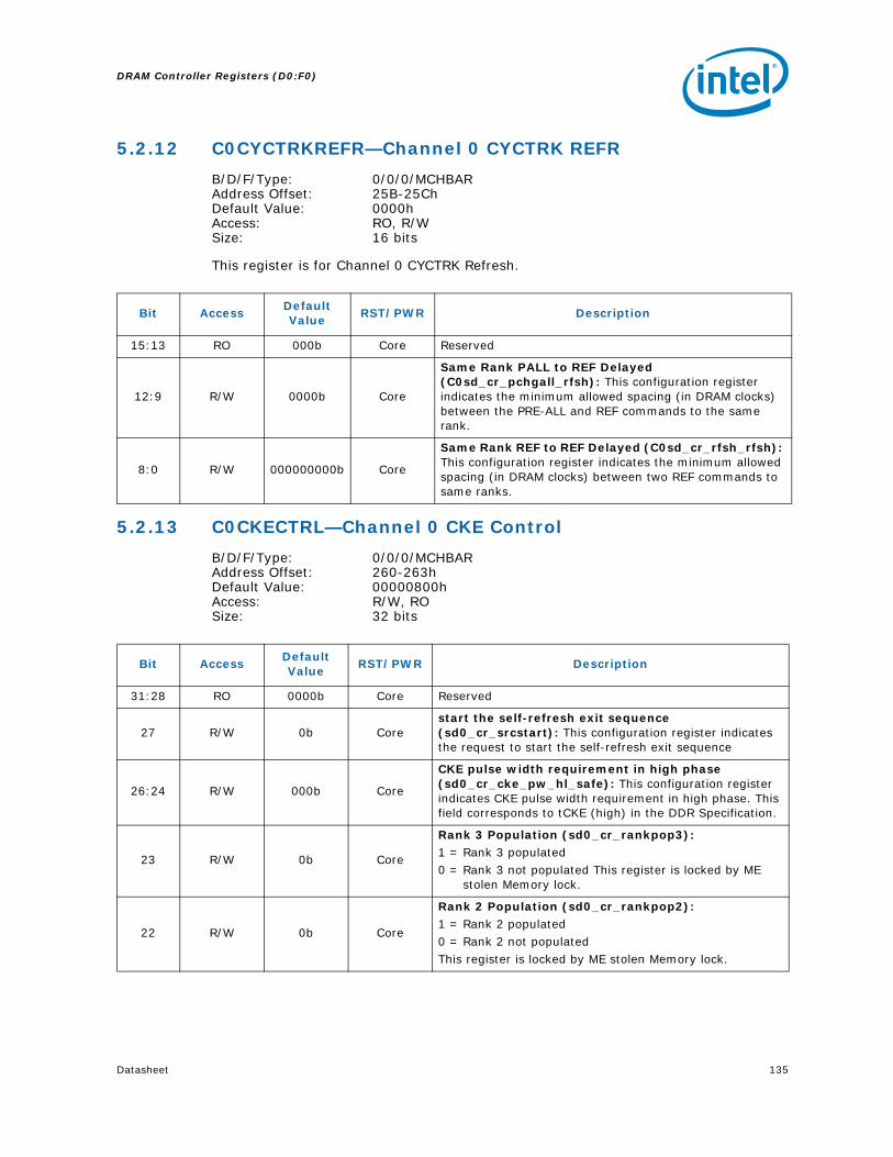
Datasheet 135
DRAM Controller Registers (D0:F0)
5.2.12 C0CYCTRKREFR—Channel 0 CYCTRK REFR
B/D/F/Type: 0/0/0/MCHBARAddress Offset: 25B-25ChDefault Value: 0000hAccess: RO, R/WSize: 16 bits
This register is for Channel 0 CYCTRK Refresh.
5.2.13 C0CKECTRL—Channel 0 CKE Control
B/D/F/Type: 0/0/0/MCHBARAddress Offset: 260-263hDefault Value: 00000800hAccess: R/W, ROSize: 32 bits
Bit AccessDefault Value
RST/PWR Description
15:13 RO 000b Core Reserved
12:9 R/W 0000b Core
Same Rank PALL to REF Delayed (C0sd_cr_pchgall_rfsh): This configuration register indicates the minimum allowed spacing (in DRAM clocks) between the PRE-ALL and REF commands to the same rank.
8:0 R/W 000000000b Core
Same Rank REF to REF Delayed (C0sd_cr_rfsh_rfsh): This configuration register indicates the minimum allowed spacing (in DRAM clocks) between two REF commands to same ranks.
Bit AccessDefault Value
RST/PWR Description
31:28 RO 0000b Core Reserved
27 R/W 0b Corestart the self-refresh exit sequence (sd0_cr_srcstart): This configuration register indicates the request to start the self-refresh exit sequence
26:24 R/W 000b Core
CKE pulse width requirement in high phase (sd0_cr_cke_pw_hl_safe): This configuration register indicates CKE pulse width requirement in high phase. This field corresponds to tCKE (high) in the DDR Specification.
23 R/W 0b Core
Rank 3 Population (sd0_cr_rankpop3): 1 = Rank 3 populated0 = Rank 3 not populated This register is locked by ME
stolen Memory lock.
22 R/W 0b Core
Rank 2 Population (sd0_cr_rankpop2): 1 = Rank 2 populated0 = Rank 2 not populatedThis register is locked by ME stolen Memory lock.

DRAM Controller Registers (D0:F0)
136 Datasheet
21 R/W 0b Core
Rank 1 Population (sd0_cr_rankpop1): 1 = Rank 1 populated0 = Rank 1 not populated This register is locked by ME stolen Memory lock.
20 R/W 0b Core
Rank 0 Population (sd0_cr_rankpop0): 1 = Rank 0 populated0 = Rank 0 not populated This register is locked by ME stolen Memory lock.
19:17 R/W 000b Core
CKE pulse width requirement in low phase (sd0_cr_cke_pw_lh_safe): This configuration register indicates CKE pulse width requirement in low phase. This field corresponds to tCKE (low) in the DDR Specification.
16 R/W 0b CoreEnable CKE toggle for PDN entry/exit (sd0_cr_pdn_enable): This configuration bit indicates that the toggling of CKEs (for PDN entry/exit) is enabled.
15:14 RO 00b Core Reserved
13:10 R/W 0010b Core
Minimum Powerdown exit to Non-Read command spacing (sd0_cr_txp): This configuration register indicates the minimum number of clocks to wait following assertion of CKE before issuing a non-read command.1010–1111=Reserved.0010–1001=2–9clocks.0000–0001=Reserved.
9:1 R/W000000000
bCore
Self refresh exit count (sd0_cr_slfrfsh_exit_cnt): This configuration register indicates the Self refresh exit count. (Program to 255). This field corresponds to tXSNR/tXSRD in the DDR Specification.
0 R/W 0b CoreIndicates Only 1 DIMM Populated (sd0_cr_singledimmpop): This configuration register indicates the that only 1 DIMM is populated.
Bit AccessDefault Value
RST/PWR Description

Datasheet 137
DRAM Controller Registers (D0:F0)
5.2.14 C0REFRCTRL—Channel 0 DRAM Refresh Control
B/D/F/Type: 0/0/0/MCHBARAddress Offset: 269-26EhDefault Value: 241830000C30hAccess: R/W, ROSize: 48 bits
This register provides settings to configure the DRAM refresh controller.
Bit AccessDefault Value
RST/PWR Description
47 RO 0b Core Reserved
46:44 R/W 010b CoreInitial Refresh Count (sd0_cr_init_refrcnt): This field specifies the initial refresh count value.
43:38 R/W 010000b Core
Direct Rcomp Quiet Window (DIRQUIET): This configuration setting indicates the amount of refresh_tick events to wait before the service of rcomp request in non-default mode of independent rank refresh.
37:32 R/W 011000b Core
Indirect Rcomp Quiet Window (INDIRQUIET): This configuration setting indicates the amount of refresh_tick events to wait before the service of rcomp request in non-default mode of independent rank refresh.
31:27 R/W 00110b Core
Rcomp Wait (RCOMPWAIT): This configuration setting indicates the amount of refresh_tick events to wait before the service of rcomp request in non-default mode of independent rank refresh.
26 R/W 0b CoreZQCAL Enable (ZQCALEN): This bit enables the DRAM controller to issue ZQCAL S command periodically.
25 R/W 0b Core
Refresh Counter Enable (REFCNTEN): This bit is used to enable the refresh counter to count during times that DRAM is not in self-refresh, but refreshes are not enabled. Such a condition may occur due to need to reprogram DIMMs following DRAM controller switch.This bit has no effect when Refresh is enabled (i.e., there is no mode where Refresh is enabled but the counter does not run). So, along with bit 23 REFEN, the modes are:REFEN:REFCNTEN Description
0:0 Normal refresh disable0:1 Refresh disabled, but counter is
accumulating refreshes.1:X Normal refresh enable
24 R/W 0b Core
All Rank Refresh (ALLRKREF): This bit enables (by default) that all the ranks are refreshed in a staggered/atomic fashion. If set, the ranks are refreshed in an independent fashion.
23 R/W 0b CoreRefresh Enable (REFEN): 0 = Disabled1 = Enabled
22 R/W 0b CoreDDR Initialization Done (INITDONE): This bit indicates that DDR initialization is complete.

DRAM Controller Registers (D0:F0)
138 Datasheet
21:20 R/W 00b Core
DRAM Refresh Hysterisis (REFHYSTERISIS): Hysterisis level - Useful for dref_high watermark cases. The dref_high flag is set when the dref_high watermark level is exceeded, and is cleared when the refresh count is less than the hysterisis level. This bit should be set to a value less than the high watermark level.00 = 301 = 410 = 511 = 6
19:18 R/W 00b Core
DRAM Refresh Panic Watermark (REFPANICWM): When the refresh count exceeds this level, a refresh request is launched to the scheduler and the dref_panic flag is set.00 = 501 = 610 = 711 = 8
17:16 R/W 00b Core
DRAM Refresh High Watermark (REFHIGHWM): When the refresh count exceeds this level, a refresh request is launched to the scheduler and the dref_high flag is set. 00 = 301 = 410 = 511 = 6
15:14 R/W 00b Core
DRAM Refresh Low Watermark (REFLOWWM): When the refresh count exceeds this level, a refresh request is launched to the scheduler and the dref_low flag is set.00 = 101 = 210 = 311 = 4
13:0 R/W001100001
10000bCore
Refresh Counter Time Out Value (REFTIMEOUT): Program this field with a value that will provide 7.8 us at the memory clock frequency. At various memory clock frequencies, this results in the following values:266 MHz -> 820 hex333 MHz -> A28 hex400 MHz -> C30 hex533 MHz -> 104B hex666 MHz -> 1450 hex
Bit AccessDefault Value
RST/PWR Description

Datasheet 139
DRAM Controller Registers (D0:F0)
5.2.15 C0ODTCTRL—Channel 0 ODT Control
B/D/F/Type: 0/0/0/MCHBARAddress Offset: 29C-29FhDefault Value: 00000000hAccess: RO, R/WSize: 32 bits
5.2.16 C1DRB1—Channel 1 DRAM Rank Boundary Address 1
B/D/F/Type: 0/0/0/MCHBARAddress Offset: 602-603hDefault Value: 0000hAccess: R/W/L, ROSize: 16 bits
The operation of this register is detailed in the description for the C0DRB0 register.
Bit AccessDefault Value
RST/PWR Description
31:12 RO 00000h Core Reserved
11:8 R/W 0000b Core
DRAM ODT for Read Commands (sd0_cr_odt_duration_rd): This field specifies the duration in memory clocks to assert DRAM ODT for Read Commands. The Async value should be used when the Dynamic Powerdown bit is set; otherwise, use the Sync value.
7:4 R/W 0000b Core
DRAM ODT for Write Commands (sd0_cr_odt_duration_wr): This field specifies the duration in memory clocks to assert DRAM ODT for Write Commands. The Async value should be used when the Dynamic Powerdown bit is set; otherwise use the Sync value.
3:0 R/W 0000b Core
MCH ODT for Read Commands (sd0_cr_mchodt_duration): This field specifies the duration in memory clocks to assert (G)MCH ODT for Read Commands.
Bit AccessDefault Value
RST/PWR Description
15:10 RO 000000b Core Reserved
9:0 R/W/L 000h Core
Channel 1 DRAM Rank Boundary Address 1 (C1DRBA1): See C0DRB1. In stacked mode, if this is the topmost populated rank in Channel 1, program this value to be cumulative of Ch0 DRB3.This register is locked by ME stolen Memory lock.

DRAM Controller Registers (D0:F0)
140 Datasheet
5.2.17 C1DRB2—Channel 1 DRAM Rank Boundary Address 2
B/D/F/Type: 0/0/0/MCHBARAddress Offset: 604-605hDefault Value: 0000hAccess: R/W/L, ROSize: 16 bits
The operation of this register is detailed in the description for the C0DRB0 register.
5.2.18 C1DRB3—Channel 1 DRAM Rank Boundary Address 3
B/D/F/Type: 0/0/0/MCHBARAddress Offset: 606-607hDefault Value: 0000hAccess: R/W, ROSize: 16 bits
The operation of this register is detailed in the description for the C0DRB0 register.
Bit AccessDefault Value
RST/PWR Description
15:10 RO 000000b Core Reserved
9:0 R/W/L 000h Core
Channel 1 DRAM Rank Boundary Address 2 (C1DRBA2): See C0DRB2. In stacked mode, if this is the topmost populated rank in Channel 1, program this value to be cumulative of Ch0 DRB3.This register is locked by ME stolen Memory lock.
Bit AccessDefault Value
RST/PWR Description
15:10 RO 000000b Core Reserved
9:0 R/W 000h Core
Channel 1 DRAM Rank Boundary Address 3 (C1DRBA3): See C0DRB3. In stacked mode, this will be cumulative of Ch0 DRB3.This register is locked by ME stolen Memory lock.

Datasheet 141
DRAM Controller Registers (D0:F0)
5.2.19 C1DRA01—Channel 1 DRAM Rank 0,1 Attributes
B/D/F/Type: 0/0/0/MCHBARAddress Offset: 608-609hDefault Value: 0000hAccess: R/W/LSize: 16 bits
The operation of this register is detailed in the description for the C0DRA01 register.
5.2.20 C1DRA23—Channel 1 DRAM Rank 2,3 Attributes
B/D/F/Type: 0/0/0/MCHBARAddress Offset: 60A-60BhDefault Value: 0000hAccess: R/W/LSize: 16 bits
The operation of this register is detailed in the description for the C0DRA01 register.
Bit AccessDefault Value
RST/PWR Description
15:8 R/W/L 00h CoreChannel 1 DRAM Rank-1 Attributes (C1DRA1): See C0DRA1.This register is locked by ME stolen Memory lock.
7:0 R/W/L 00h CoreChannel 1 DRAM Rank-0 Attributes (C1DRA0): See C0DRA0.This register is locked by ME stolen Memory lock.
Bit AccessDefault Value
RST/PWR Description
15:8 R/W/L 00h CoreChannel 1 DRAM Rank-3 Attributes (C1DRA3): See C0DRA3. This register is locked by ME stolen Memory lock.
7:0 R/W/L 00h CoreChannel 1 DRAM Rank-2 Attributes (C1DRA2): See C0DRA2.This register is locked by ME stolen Memory lock.

DRAM Controller Registers (D0:F0)
142 Datasheet
5.2.21 C1CYCTRKPCHG—Channel 1 CYCTRK PCHG
B/D/F/Type: 0/0/0/MCHBARAddress Offset: 650-651hDefault Value: 0000hAccess: R/W, ROSize: 16 bits
Bit AccessDefault Value
RST/PWR Description
15:11 RO 00000b Core Reserved.
10:6 R/W 00000b Core
Write To PRE Delayed (C1sd_cr_wr_pchg): This field indicates the minimum allowed spacing (in DRAM clocks) between the WRITE and PRE commands to the same rank-bank. This field corresponds to tWR in the DDR Specification.
5:2 R/W 0000b Core
READ To PRE Delayed (C1sd_cr_rd_pchg): This field indicates the minimum allowed spacing (in DRAM clocks) between the READ and PRE commands to the same rank-bank
1:0 R/W 00b CorePRE To PRE Delayed (C1sd_cr_pchg_pchg): This field indicates the minimum allowed spacing (in DRAM clocks) between two PRE commands to the same rank.

Datasheet 143
DRAM Controller Registers (D0:F0)
5.2.22 C1CYCTRKACT—Channel 1 CYCTRK ACT
B/D/F/Type: 0/0/0/MCHBARAddress Offset: 652-655hDefault Value: 00000000hAccess: R/W, ROSize: 32 bits
Bit AccessDefault Value
RST/PWR Description
31:30 RO 0h Core Reserved
29 R/W 0b Core
FAW Windowcnt Bug Fix Disable (C1sd_cr_cyctrk_faw_windowcnt_fix_disable): This field disables the CYCTRK FAW windowcnt bug fix.1 = Disable CYCTRK FAW windowcnt bug fix0 = Enable CYCTRK FAW windowcnt bug fix
28 R/W 0b Core
FAW Phase Bug Fix Disable (C1sd_cr_cyctrk_faw_phase_fix_disable): This field disables the CYCTRK FAW phase indicator bug fix.1 = Disable CYCTRK FAW phase indicator bug fix0 = Enable CYCTRK FAW phase indicator bug fix
27:22 R/W 000000b Core
ACT Window Count (C1sd_cr_act_windowcnt): This field indicates the window duration (in DRAM clocks) during which the controller counts the # of activate commands which are launched to a particular rank. If the number of activate commands launched within this window is greater than 4, then a check is implemented to block launch of further activates to this rank for the rest of the duration of this window.
21 R/W 0b CoreMax ACT Check (C1sd_cr_maxact_dischk): This field enables the check which ensures that there are no more than four activates to a particular rank in a given window.
20:17 R/W 0000b Core
ACT to ACT Delayed (C1sd_cr_act_act[): This field indicates the minimum allowed spacing (in DRAM clocks) between two ACT commands to the same rank. This field corresponds to tRRD in the DDR Specification.
16:13 R/W 0000b Core
PRE to ACT Delayed (C1sd_cr_pre_act): This field indicates the minimum allowed spacing (in DRAM clocks) between the PRE and ACT commands to the same rank-bank:12:9R/W0000bPRE-ALL to ACT Delayed (C1sd_cr_preall_act):. This configuration register indicates the minimum allowed spacing (in DRAM clocks) between the PRE-ALL and ACT commands to the same rank. This field corresponds to tRP in the DDR Specification.
12:9 R/W 0h Core
ALLPRE to ACT Delay (C1sd_cr_preall_act): From the launch of a prechargeall command wait for this number of memory clocks before launching a activate command. This field corresponds to tPALL_RP in the DDR specification.
8:0 R/W 000000000b Core
REF to ACT Delayed (C1sd_cr_rfsh_act): This field indicates the minimum allowed spacing (in DRAM clocks) between REF and ACT commands to the same rank. This field corresponds to tRFC in the DDR Specification.

DRAM Controller Registers (D0:F0)
144 Datasheet
5.2.23 C1CYCTRKWR—Channel 1 CYCTRK WR
B/D/F/Type: 0/0/0/MCHBARAddress Offset: 656-657hDefault Value: 0000hAccess: R/WSize: 16 bits
Bit AccessDefault Value
RST/PWR Description
15:12 R/W 0h Core
ACT To Write Delay (C1sd_cr_act_wr): This field indicates the minimum allowed spacing (in DRAM clocks) between the ACT and WRITE commands to the same rank-bank. This field corresponds to tRCD_wr in the DDR Specification.
11:8 R/W 0h Core
Same Rank Write To Write Delayed (C1sd_cr_wrsr_wr): This field indicates the minimum allowed spacing (in DRAM clocks) between two WRITE commands to the same rank.
7:4 R/W 0h Core
Different Rank Write to Write Delay (C1sd_cr_wrdr_wr): This field indicates the minimum allowed spacing (in DRAM clocks) between two WRITE commands to different ranks. This field corresponds to tWR_WR in the DDR Specification.
3:0 R/W 0h Core
READ To WRTE Delay (C1sd_cr_rd_wr): This field indicates the minimum allowed spacing (in DRAM clocks) between the READ and WRITE commands. This field corresponds to tRD_WR in the DDR specification.

Datasheet 145
DRAM Controller Registers (D0:F0)
5.2.24 C1CYCTRKRD—Channel 1 CYCTRK READ
B/D/F/Type: 0/0/0/MCHBARAddress Offset: 658-65AhDefault Value: 000000hAccess: R/W, ROSize: 24 bits
5.2.25 C1CKECTRL—Channel 1 CKE Control
B/D/F/Type: 0/0/0/MCHBARAddress Offset: 660-663hDefault Value: 00000800hAccess: R/W, ROSize: 32 bits
Bit AccessDefault Value
RST/PWR Description
23:21 RO 0h Core Reserved
20:17 R/W 0h Core
Min ACT To READ Delayed (C1sd_cr_act_rd): This field indicates the minimum allowed spacing (in DRAM clocks) between the ACT and READ commands to the same rank-bank. This field corresponds to tRCD_rd in the DDR Specification.
16:12 R/W 00000b Core
Same Rank Write To READ Delayed (C1sd_cr_wrsr_rd): This field indicates the minimum allowed spacing (in DRAM clocks) between the WRITE and READ commands to the same rank. This field corresponds to tWTR in the DDR Specification.
11:8 R/W 0000b Core
Different Ranks Write To READ Delayed (C1sd_cr_wrdr_rd): This field indicates the minimum allowed spacing (in DRAM clocks) between the WRITE and READ commands to different ranks. This field corresponds to tWR_RD in the DDR Specification.
7:4 R/W 0000b Core
Same Rank Read To Read Delayed (C1sd_cr_rdsr_rd): This field indicates the minimum allowed spacing (in DRAM clocks) between two READ commands to the same rank.
3:0 R/W 0000b Core
Different Ranks Read To Read Delayed (C1sd_cr_rddr_rd): This field indicates the minimum allowed spacing (in DRAM clocks) between two READ commands to different ranks. This field corresponds to tRD_RD in the DDR Specification.
Bit AccessDefault Value
RST/PWR Description
31:28 RO 0h Core Reserved
27 R/W 0b Corestart the self-refresh exit sequence (sd1_cr_srcstart): This field indicates the request to start the self-refresh exit sequence
26:24 R/W 000b Core
CKE pulse width requirement in high phase (sd1_cr_cke_pw_hl_safe): This field indicates CKE pulse width requirement in high phase. This field corresponds to tCKE (high) in the DDR Specification.

DRAM Controller Registers (D0:F0)
146 Datasheet
23 R/W 0b Core
Rank 3 Population (sd1_cr_rankpop3): 1 = Rank 3 populated0 = Rank 3 not populated This register is locked by ME stolen Memory lock.
22 R/W 0b Core
Rank 2 Population (sd1_cr_rankpop2): 1 = Rank 2 populated0 = Rank 2 not populatedThis register is locked by ME stolen Memory lock.
21 R/W 0b Core
Rank 1 Population (sd1_cr_rankpop1): 1 = Rank 1 populated0 = Rank 1 not populated This register is locked by ME stolen Memory lock.
20 R/W 0b Core
Rank 0 Population (sd1_cr_rankpop0): 1 = Rank 0 populated0 = Rank 0 not populatedThis register is locked by ME stolen Memory lock.
19:17 R/W 000b Core
CKE pulse width requirement in low phase (sd1_cr_cke_pw_lh_safe): This field indicates CKE pulse width requirement in low phase. This field corresponds to tCKE (low) in the DDR Specification.
16 R/W 0b CoreEnable CKE toggle for PDN entry/exit (sd1_cr_pdn_enable): This bit indicates that the toggling of CKEs (for PDN entry/exit) is enabled.
15:14 RO 00b Core Reserved
13:10 R/W 0010b Core
Minimum Powerdown Exit to Non-Read command spacing (sd1_cr_txp): This configuration register indicates the minimum number of clocks to wait following assertion of CKE before issuing a non-read command.1010–1111 = Reserved.0010–1001 = 2–9 clocks0000–0001 = Reserved.
9:1 R/W 000000000b Core
Self refresh exit count (sd1_cr_slfrfsh_exit_cnt): This field indicates the Self refresh exit count. (Program to 255). This field corresponds to tXSNR/tXSRD in the DDR Specification.
0 R/W 0b CoreIndicates Only 1 DIMM Populated (sd1_cr_singledimmpop): This field indicates the that only 1 DIMM is populated.
Bit AccessDefault Value
RST/PWR Description

Datasheet 147
DRAM Controller Registers (D0:F0)
5.2.26 C1REFRCTRL—Channel 1 DRAM Refresh Control
B/D/F/Type: 0/0/0/MCHBARAddress Offset: 669-66EhDefault Value: 241830000C30hAccess: R/W, ROSize: 48 bits
This register provides settings to configure the DRAM refresh controller.
Bit AccessDefault Value
RST/PWR Description
47 RO 0b Core Reserved
46:44 R/W 010b CoreInitial Refresh Count (sd1_cr_init_refrcnt): This field specifies the initial refresh count value.
43:38 R/W 010000b Core
Direct Rcomp Quiet Window (DIRQUIET): This configuration setting indicates the amount of refresh_tick events to wait before the service of rcomp request in non-default mode of independent rank refresh.
37:32 R/W 011000b Core
Indirect Rcomp Quiet Window (INDIRQUIET): This configuration setting indicates the amount of refresh_tick events to wait before the service of rcomp request in non-default mode of independent rank refresh.
31:27 R/W 00110b Core
Rcomp Wait (RCOMPWAIT): This configuration setting indicates the amount of refresh_tick events to wait before the service of rcomp request in non-default mode of independent rank refresh.
26 R/W 0b CoreZQCAL Enable (ZQCALEN): This bit enables the DRAM controller to issue ZQCAL S command periodically.
25 R/W 0b Core
Refresh Counter Enable (REFCNTEN): This bit is used to enable the refresh counter to count during times that DRAM is not in self-refresh, but refreshes are not enabled. Such a condition may occur due to need to reprogram DIMMs following DRAM controller switch.This bit has no effect when Refresh is enabled (i.e. there is no mode where Refresh is enabled but the counter does not run) So, in conjunction with bit 23 REFEN, the modes are:REFEN:REFCNTEN Description
0:0 Normal refresh disable0:1 Refresh disabled, but counter is
accumulating refreshes.1:X Normal refresh enable
24 R/W 0b Core
All Rank Refresh (ALLRKREF): This configuration bit enables (by default) that all the ranks are refreshed in a staggered/atomic fashion. If set, the ranks are refreshed in an independent fashion.
23 R/W 0b Core
Refresh Enable (REFEN):
0 = Disabled
1 = Enabled
22 R/W 0b CoreDDR Initialization Done (INITDONE): This bit indicates that DDR initialization is complete.

DRAM Controller Registers (D0:F0)
148 Datasheet
21:20 R/W 00b Core
DRAM Refresh Hysterisis (REFHYSTERISIS): Hysterisis level - Useful for dref_high watermark cases. The dref_high flag is set when the dref_high watermark level is exceeded, and is cleared when the refresh count is less than the hysterisis level. This bit should be set to a value less than the high watermark level.00 = 301 = 410 = 511 = 6
19:18 R/W 00b Core
DRAM Refresh Panic Watermark (REFPANICWM): When the refresh count exceeds this level, a refresh request is launched to the scheduler and the dref_panic flag is set.00 = 501 = 610 = 711 = 8
17:16 R/W 00b Core
DRAM Refresh High Watermark (REFHIGHWM): When the refresh count exceeds this level, a refresh request is launched to the scheduler and the dref_high flag is set.00 = 301 = 410 = 511 = 6
15:14 R/W 00b Core
DRAM Refresh Low Watermark (REFLOWWM): When the refresh count exceeds this level, a refresh request is launched to the scheduler and the dref_low flag is set.00 = 101 = 210 = 311 = 4
13:0 R/W001100001
10000bCore
Refresh Counter Time Out Value (REFTIMEOUT): Program this field with a value that will provide 7.8 us at the memory clock frequency. At various memory frequencies this results in the following values:266 MHz -> 820 hex333 MHz -> A28 hex400 MHz -> C30 hex533 MHz -> 104B hex666 MHz -> 1450 hex
Bit AccessDefault Value
RST/PWR Description

Datasheet 149
DRAM Controller Registers (D0:F0)
5.2.27 C1ODTCTRL—Channel 1 ODT Control
B/D/F/Type: 0/0/0/MCHBARAddress Offset: 69C-69FhDefault Value: 00000000hAccess: R/W, ROSize: 32 bits
5.2.28 EPC0DRB0—EP Channel 0 DRAM Rank Boundary Address 0
B/D/F/Type: 0/0/0/MCHBARAddress Offset: A00-A01hDefault Value: 0000hAccess: R/W, ROSize: 16 bits
Bit AccessDefault Value
RST/PWR Description
31:12 RO 00000h Core Reserved
11:8 R/W 0h Core
DRAM ODT for Read Commands (sd1_cr_odt_duration_rd): This field specifies the duration in memory clocks to assert DRAM ODT for Read Commands. The Async value should be used when the Dynamic Powerdown bit is set; otherwise use the Sync value.
7:4 R/W 0h Core
DRAM ODT for Write Commands (sd1_cr_odt_duration_wr): This field specifies the duration in memory clocks to assert DRAM ODT for Write Commands. The Async value should be used when the Dynamic Powerdown bit is set; otherwise, use the Sync value.
3:0 R/W 0h Core
MCH ODT for Read Commands (sd1_cr_mchodt_duration): This field specifies the duration in memory clocks to assert (G)MCH ODT for Read Commands.
Bit Access Default Value
RST/PWR
Description
15:10 RO 000000b Core Reserved
9:0 R/W 000h CoreChannel 0 Dram Rank Boundary Address 0 (C0DRBA0):

DRAM Controller Registers (D0:F0)
150 Datasheet
5.2.29 EPC0DRB1—EP Channel 0 DRAM Rank Boundary Address 1
B/D/F/Type: 0/0/0/MCHBARAddress Offset: A02-A03hDefault Value: 0000hAccess: RO, R/WSize: 16 bits
See C0DRB0 register for description.
5.2.30 EPC0DRB2—EP Channel 0 DRAM Rank Boundary Address 2
B/D/F/Type: 0/0/0/MCHBARAddress Offset: A04-A05hDefault Value: 0000hAccess: RO, R/WSize: 16 bits
See C0DRB0 register for description.
5.2.31 EPC0DRB3—EP Channel 0 DRAM Rank Boundary Address 3
B/D/F/Type: 0/0/0/MCHBARAddress Offset: A06-A07hDefault Value: 0000hAccess: R/W, ROSize: 16 bits
See C0DRB0 register for description.
Bit AccessDefault Value
RST/PWR Description
15:10 RO 000000b Core Reserved
9:0 R/W 000h CoreChannel 0 Dram Rank Boundary Address 1 (C0DRBA1):
Bit AccessDefault Value
RST/PWR Description
15:10 RO 000000b Core Reserved
9:0 R/W 000h CoreChannel 0 DRAM Rank Boundary Address 2 (C0DRBA2):
Bit Access Default Value
RST/PWR
Description
15:10 RO 000000b Core Reserved
9:0 R/W 000h Core Channel 0 DRAM Rank Boundary Address 3 (C0DRBA3):

Datasheet 151
DRAM Controller Registers (D0:F0)
5.2.32 EPC0DRA01—EP Channel 0 DRAM Rank 0,1 Attribute
B/D/F/Type: 0/0/0/MCHBARAddress Offset: A08-A09hDefault Value: 0000hAccess: R/WSize: 16 bits
The DRAM Rank Attribute Registers define the page sizes/number of banks to be used when accessing different ranks. These registers should be left with their default value (all zeros) for any rank that is unpopulated, as determined by the corresponding CxDRB registers. Each byte of information in the CxDRA registers describes the page size of a pair of ranks. Channel and rank map:
Ch0 Rank0, 1: 108h–109hCh0 Rank2, 3: 10Ah–10BhCh1 Rank0, 1: 188h–189hCh1 Rank2, 3: 18Ah–18Bh
5.2.33 EPC0DRA23—EP Channel 0 DRAM Rank 2,3 Attribute
B/D/F/Type: 0/0/0/MCHBARAddress Offset: A0A-A0BhDefault Value: 0000hAccess: R/WSize: 16 bits
See C0DRA01 for detailed descriptions.
Bit AccessDefault Value
RST/PWR Description
15:8 R/W 00h CoreChannel 0 DRAM Rank-1 Attributes (C0DRA1): This field defines DRAM pagesize/number-of-banks for rank1 for given channel.
7:0 R/W 00h CoreChannel 0 DRAM Rank-0 Attributes (C0DRA0): This field defines DRAM pagesize/number-of-banks for rank0 for given channel.
Bit AccessDefault Value
RST/PWR Description
15:8 R/W 00h CoreChannel 0 DRAM Rank-3 Attributes (C0DRA3): This field defines DRAM pagesize/number-of-banks for rank3 for given channel.
7:0 R/W 00h CoreChannel 0 DRAM Rank-2 Attributes (C0DRA2): This field defines DRAM pagesize/number-of-banks for rank2 for given channel.

DRAM Controller Registers (D0:F0)
152 Datasheet
5.2.34 EPDCYCTRKWRTPRE—EPD CYCTRK WRT PRE
B/D/F/Type: 0/0/0/MCHBARAddress Offset: A19-A1AhDefault Value: 0000hAccess: R/W, ROSize: 16 bits
5.2.35 EPDCYCTRKWRTACT—EPD CYCTRK WRT ACT
B/D/F/Type: 0/0/0/MCHBARAddress Offset: A1C-A1FhDefault Value: 00000000hAccess: RO, R/WSize: 32 bits
Bit AccessDefault Value
RST/PWR Description
15:11 R/W 00000b Core
ACT To PRE Delayed (C0sd_cr_act_pchg): This field indicates the minimum allowed spacing (in DRAM clocks) between the ACT and PRE commands to the same rank-bank.
10:6 R/W 00000b Core
Write To PRE Delayed (C0sd_cr_wr_pchg): This field indicates the minimum allowed spacing (in DRAM clocks) between the WRITE and PRE commands to the same rank-bank.
5:2 R/W 0000b Core
READ To PRE Delayed (C0sd_cr_rd_pchg): This field indicates the minimum allowed spacing (in DRAM clocks) between the READ and PRE commands to the same rank-bank.
1:0 RO 00b Core Reserved
Bit AccessDefault Value
RST/PWR Description
31:21 RO 000h Core Reserved
20:17 R/W 0000b CoreACT to ACT Delayed (C0sd_cr_act_act[): This field indicates the minimum allowed spacing (in DRAM clocks) between two ACT commands to the same rank.
16:13 R/W 0000b Core
PRE to ACT Delayed (C0sd_cr_pre_act): This field indicates the minimum allowed spacing (in DRAM clocks) between the PRE and ACT commands to the same rank-bank:12:9R/W0000bPRE-ALL to ACT Delayed (C0sd_cr_preall_act):. This configuration register indicates the minimum allowed spacing (in DRAM clocks) between the PRE-ALL and ACT commands to the same rank.
12:9 RO 0h Core Reserved
8:0 R/W 000000000b CoreREF to ACT Delayed (C0sd_cr_rfsh_act): This field indicates the minimum allowed spacing (in DRAM clocks) between REF and ACT commands to the same rank.

Datasheet 153
DRAM Controller Registers (D0:F0)
5.2.36 EPDCYCTRKWRTWR—EPD CYCTRK WRT WR
B/D/F/Type: 0/0/0/MCHBARAddress Offset: A20-A21hDefault Value: 0000hAccess: R/W, ROSize: 16 bits
5.2.37 EPDCYCTRKWRTREF—EPD CYCTRK WRT REF
B/D/F/Type: 0/0/0/MCHBARAddress Offset: A22-A23hDefault Value: 0000hAccess: RO, R/WSize: 16 bitsBIOS Optimal Default 0h
EPD CYCTRK WRT ACT Status Register.
Bit AccessDefault Value
RST/PWR Description
15:12 R/W 0h Core
ACT To Write Delay (C0sd_cr_act_wr): This field indicates the minimum allowed spacing (in DRAM clocks) between the ACT and WRITE commands to the same rank-bank.
11:8 R/W 0h Core
Same Rank Write To Write Delayed (C0sd_cr_wrsr_wr): This field indicates the minimum allowed spacing (in DRAM clocks) between two WRITE commands to the same rank.
7:4 RO 0h Core Reserved
3:0 R/W 0h Core
Same Rank WRITE to READ Delay (C0sd_cr_rd_wr): This field indicates the minimum allowed spacing (in DRAM clocks) between the WRITE and READ commands to the same rank.
Bit AccessDefault Value
RST/PWR Description
15:13 RO 000b Core Reserved
12:9 RO 0h Reserved
8:0 R/W 000000000b Core
Different Rank REF to REF Delayed (C0sd_cr_rfsh_rfsh): This field indicates the minimum allowed spacing (in DRAM clocks) between two REF commands to different ranks.

DRAM Controller Registers (D0:F0)
154 Datasheet
5.2.38 EPDCYCTRKWRTRD—EPD CYCTRK WRT READ
B/D/F/Type: 0/0/0/MCHBARAddress Offset: A24-A26hDefault Value: 000000hAccess: R/WSize: 24 bitsBIOS Optimal Default 000h
Bit AccessDefault Value
RST/PWR Description
23:23 RO 0h Reserved
22:20 R/W 000b CoreEPDunit DQS Slave DLL Enable to Read Safe (EPDSDLL2RD): This field provides setting for Read command safe from the point of enabling the slave DLLs.
19:18 RO 0h Reserved
17:14 R/W 0h Core
Min ACT To READ Delayed (C0sd_cr_act_rd): This field indicates the minimum allowed spacing (in DRAM clocks) between the ACT and READ commands to the same rank-bank
13:9 R/W 00000b Core
Same Rank READ to WRITE Delayed (C0sd_cr_wrsr_rd): This field indicates the minimum allowed spacing (in DRAM clocks) between the READ and WRITE commands.
8:6 RO 0h Reserved
5:3 R/W 000b Core
Same Rank Read To Read Delayed (C0sd_cr_rdsr_rd): This field indicates the minimum allowed spacing (in DRAM clocks) between two READ commands to the same rank.
2:0 RO 0h Reserved

Datasheet 155
DRAM Controller Registers (D0:F0)
5.2.39 EPDCKECONFIGREG—EPD CKE Related Configuration Registers
B/D/F/Type: 0/0/0/MCHBARAddress Offset: A28-A2ChDefault Value: 00E0000000hAccess: R/WSize: 40 bitsBIOS Optimal Default 0h
Bit AccessDefault Value
RST/PWR Description
39:35 R/W 00000b Core
EPDunit TXPDLL Count (EPDTXPDLL): This field specifies the delay from precharge power down exit to a command that requires the DRAM DLL to be operational. The commands are read/write.
34:32 R/W 000b Core
EPDunit TXP count (EPDCKETXP): This field specifies the timing requirement for Active power down exit or fast exit pre-charge power down exit to any command or slow exit pre-charge power down to Non-DLL (rd/wr/odt). command.
31:29 R/W 111b Core
Mode Select (sd0_cr_sms): Mode Select register: This field setting indicates the mode in which the controller is operating in.111 = Indicates normal mode of operation, else special
mode of operation.
28:27 R/W 00b Core
EPDunit EMRS command select. (EPDEMRSSEL): EMRS mode to select BANK address.01 = EMRS10 = EMRS211 = EMRS3
26:24 R/W 000b CoreCKE pulse width requirement in high phase (sd0_cr_cke_pw_hl_safe): This field indicates CKE pulse width requirement in high phase.
23:20 R/W 0h Coreone-hot active rank population (ep_scr_actrank): This field indicates the active rank in a one hot manner.
19:17 R/W 000b CoreCKE pulse width requirement in low phase (sd0_cr_cke_pw_lh_safe): This field indicates CKE pulse width requirement in low phase.
16:15 RO 0h Reserved
14 R/W 0b Core
EPDunit MPR mode (EPDMPR):1 = MPR mode0 = Normal modeIn MPR mode, only read cycles must be issued by Firmware. Page Results are ignored by DCS and just issues the read chip select.
13 R/W 0b Core
EPDunit Power Down enable for ODT Rank (EPDOAPDEN): This bit enables the ODT ranks to dynamically enter power down.1 = Enable active power down.0 = Disable active power down.

DRAM Controller Registers (D0:F0)
156 Datasheet
5.2.40 EPDREFCONFIG—EP DRAM Refresh Configuration
B/D/F/Type: 0/0/0/MCHBARAddress Offset: A30-A33hDefault Value: 40000C30hAccess: RO, R/WSize: 32 bits
12 R/W 0b Core
EPDunit Power Down enable for Active Rank (EPDAAPDEN): This bit enables the active rank to dynamically enter power down.1 = Enable active power down.0 = Disable active power down.
11:10 RO 0h Reserved
9:1 R/W0000000
00bCore
Self refresh exit count (sd0_cr_slfrfsh_exit_cnt): This field indicates the Self refresh exit count. Program to 255.
0 R/W 0b Core
indicates only 1 rank enabled (sd0_cr_singledimmpop): This field indicates that only 1 rank is enabled. This bit needs to be set if there is one active rank and no odt ranks, or if there is one active rank and one odt rank and they are the same rank.
Bit AccessDefault Value
RST/PWR Description
Bit AccessDefault Value
RST/PWR Description
31 RO 0b Core Reserved
30:29 R/W 10b Core
EPDunit refresh count addition for self refresh exit. (EPDREF4SR): This field indicates the number of additional refreshes that needs to be added to the refresh request count after exiting self refresh.Typical value is to add 2 refreshes.00 = Add 0 Refreshes01 = Add 1 Refreshes10 = Add 2 Refreshes11 = Add 3 Refreshes
28 R/W 0b Core
Refresh Counter Enable (REFCNTEN): This bit is used to enable the refresh counter to count during times that DRAM is not in self-refresh, but refreshes are not enabled. Such a condition may occur due to need to reprogram DIMMs following DRAM controller switch.This bit has no effect when Refresh is enabled (i.e. there is no mode where Refresh is enabled but the counter does not run) So, in conjunction with bit 23 REFEN, the modes are:REFEN:REFCNTEN Description
0:0 Normal refresh disable0:1 Refresh disabled, but counter is
accumulating refreshes.1:X Normal refresh enable

Datasheet 157
DRAM Controller Registers (D0:F0)
27 R/W 0b CoreRefresh Enable (REFEN): 0 = Disabled1 = Enabled
26 R/W 0b CoreDDR Initialization Done (INITDONE): This bit indicates that DDR initialization is complete.
25:22 R/W 0000b Core
DRAM Refresh Hysterisis (REFHYSTERISIS): Hysterisis level - Useful for dref_high watermark cases. The dref_high flag is set when the dref_high watermark level is exceeded, and is cleared when the refresh count is less than the hysterisis level. This bit should be set to a value less than the high watermark level.0000 = 00001 = 1.......1000 = 8
21:18 R/W 0000b Core
DRAM Refresh High Watermark (REFHIGHWM): When the refresh count exceeds this level, a refresh request is launched to the scheduler and the dref_high flag is set.0000 = 00001 = 1.......1000 = 8
17:14 R/W 0000b Core
DRAM Refresh Low Watermark (REFLOWWM): When the refresh count exceeds this level, a refresh request is launched to the scheduler and the dref_low flag is set.0000 = 00001 = 1.......1000 = 8
13:0 R/W001100001
10000bCore
Refresh Counter Time Out Value (REFTIMEOUT): Program this field with a value that will provide 7.8 us at the memory clock frequency.At various memory clock frequencies this results in the following values:266 MHz -> 820 hex333 MHz -> A28 hex400 MHz -> C30 hex533 MHz -> 104B hex666 MHz -> 1450 hex
Bit AccessDefault Value
RST/PWR Description

DRAM Controller Registers (D0:F0)
158 Datasheet
5.2.41 TSC1—Thermal Sensor Control 1
B/D/F/Type: 0/0/0/MCHBARAddress Offset: CD8hDefault Value: 00hAccess: R/W/L, R/W, RS/WCSize: 8 bits
This register controls the operation of the thermal sensor.
Bits 7:1 of this register are reset to their defaults by MPWROK.
Bit 0 is reset to its default by PLTRST#.
Bit AccessDefault Value
RST/PWR Description
7 R/W/L 0b Core
Thermal Sensor Enable (TSE): This bit enables power to the thermal sensor. Lockable via TCO bit 7.0 = Disabled1 = Enabled
6 R/W 0b Core
Analog Hysteresis Control (AHC): This bit enables the analog hysteresis control to the thermal sensor. When enabled, about 1 degree of hysteresis is applied. This bit should normally be off in thermometer mode since the thermometer mode of the thermal sensor defeats the usefulness of analog hysteresis.0 = hysteresis disabled1= analog hysteresis enabled.
5:2 R/W 0000b Core
Digital Hysteresis Amount (DHA): This bit determines whether no offset, 1 LSB, 2... 15 is used for hysteresis for the trip points.0000 = digital hysteresis disabled, no offset added to trip
temperature0001 = offset is 1 LSB added to each trip temperature
when tripped...0110 = ~3.0 °C (Recommended setting)...1110 = added to each trip temperature when tripped1111 = added to each trip temperature when tripped
1 R/W/L 0b Core
Thermal Sensor Comparator Select (TSCS): This bit multiplexes between the two analog comparator outputs. Normally Catastrophic is used. Lockable via TCO bit 7.0 = Catastrophic1 = Hot

Datasheet 159
DRAM Controller Registers (D0:F0)
5.2.42 TSC2—Thermal Sensor Control 2
B/D/F/Type: 0/0/0/MCHBARAddress Offset: CD9hDefault Value: 00hAccess: R/W/L, ROSize: 8 bits
This register controls the operation of the thermal sensor.
All bits in this register are reset to their defaults by MPWROK.
0 RS/WC 0b Core
In Use (IU): Software semaphore bit.After a full (G)MCH RESET, a read to this bit returns a 0.After the first read, subsequent reads will return a 1.A write of a 1 to this bit will reset the next read value to 0. Writing a 0 to this bit has no effect.Software can poll this bit until it reads a 0, and will then own the usage of the thermal sensor.This bit has no other effect on the hardware, and is only used as a semaphore among various independent software threads that may need to use the thermal sensor.Software that reads this register but does not intend to claim exclusive access of the thermal sensor must write a one to this bit if it reads a 0, in order to allow other software threads to claim it.See also THERM3 bit 7 and IUB, which are independent additional semaphore bits.
Bit AccessDefault Value
RST/PWR Description

DRAM Controller Registers (D0:F0)
160 Datasheet
Bit AccessDefault Value
RST/PWR Description
7:4 RO 0h Core Reserved
3:0 R/W/L 0h Core
Thermometer Mode Enable and Rate (TE): If analog thermal sensor mode is not enabled by setting these bits to 0000b, these bits enable the thermometer mode functions and set the Thermometer controller rate.When the Thermometer mode is disabled and TSC1[TSE] =enabled, the analog sensor mode should be fully functional. In the analog sensor mode, the Catastrophic trip is functional, and the Hot trip is functional at the offset below the catastrophic programmed into TSC2[CHO]. The other trip points are not functional in this mode.When Thermometer mode is enabled, all the trip points (Catastrophic, Hot, Aux0) will all operate using the programmed trip points and Thermometer mode rate.
NOTE:1. When disabling the Thermometer mode while
thermometer running, the Thermometer mode controller will finish the current cycle.
2. During boot, all other thermometer mode registers (except lock bits) should be programmed appropriately before enabling the Thermometer Mode.
Clocks are memory clocks.NOTE: Since prior (G)MCHs counted the thermometer rate
in terms of host clocks rather than memory clocks, the clock count for each setting listed below has been doubled from what is was on those (G)MCHs. This should make the actual thermometer rate approximately equivalent across products.
Lockable via TCO bit 7.0000 = Thermometer mode disabled (i.e, analog sensor
mode)0001 = enabled, 512 clock mode0010 = enabled, 1024 clock mode (normal Thermometer
mode operation),provides ~3.85 us settling time @ 266 MHzprovides ~3.08 us settling time @ 333 MHzprovides ~2.56 us settling time @ 400 MHz
0011 = enabled, 1536 clock mode0100 = enabled, 2048 clock mode0101 = enabled, 3072 clock mode0110 = enabled, 4096 clock mode0111 = enabled, 6144 clock mode
provides ~23.1 us settling time @ 266 MHzprovides ~18.5 us settling time @ 333 MHzprovides ~15.4 us settling time @ 400 MHz
all other permutations reserved1111 = enabled, 4 clock mode (for testing digital logic)

Datasheet 161
DRAM Controller Registers (D0:F0)
5.2.43 TSS—Thermal Sensor Status
B/D/F/Type: 0/0/0/MCHBARAddress Offset: CDAhDefault Value: 00hAccess: ROSize: 8 bits
This read only register provides trip point and other status of the thermal sensor.
All bits in this register are reset to their defaults by MPWROK.
Bit AccessDefault Value
RST/PWR Description
7 RO 0b CoreCatastrophic Trip Indicator (CTI): 1 = Internal thermal sensor temperature is above the
catastrophic setting.
6 RO 0b CoreHot Trip Indicator (HTI): 1 = Internal thermal sensor temperature is above the Hot
setting.
5 RO 0b CoreAux0 Trip Indicator (A0TI): 1 = A 1 indicates that the internal thermal sensor
temperature is above the Aux0 setting.
4 RO 0b Core
Thermometer Mode Output Valid (TOV): 1 = Thermometer mode is able to converge to a
temperature and that the TR register is reporting a reasonable estimate of the thermal sensor temperature.
0 = Thermometer mode is off, or that temperature is out of range, or that the TR register is being looked at before a temperature conversion has had time to complete.
3:2 RO 00b Core Reserved
1 RO 0b Core
Direct Catastrophic Comparator Read (DCCR): This bit reads the output of the Catastrophic comparator directly, without latching via the Thermometer mode circuit. Used for testing.
0 RO 0b CoreDirect Hot Comparator Read (DHCR): This bit reads the output of the Hot comparator directly, without latching via the Thermometer mode circuit. Used for testing.

DRAM Controller Registers (D0:F0)
162 Datasheet
5.2.44 TSTTP—Thermal Sensor Temperature Trip Point
B/D/F/Type: 0/0/0/MCHBARAddress Offset: CDC-CDFhDefault Value: 00000000hAccess: RO, R/W, R/W/LSize: 32 bits
This register:
1. Sets the target values for the trip points in thermometer mode. See also TST [Direct DAC Connect Test Enable].
2. Reports the relative thermal sensor temperature
All bits in this register are reset to their defaults by MPWROK.
Bit AccessDefault Value
RST/PWR Description
31:24 RO 00h Core
Relative Temperature (RELT): In Thermometer mode, the RELT field of this register report the relative temperature of the thermal sensor. Provides a two's complement value of the thermal sensor relative to the Hot Trip Point. Temperature above the Hot Trip Point will be positive.TR and HTPS can both vary between 0 and 255. But RELT will be clipped between ±127 to keep it an 8 bit number.See also TSS[Thermometer mode Output Valid]In the Analog mode, the RELT field reports HTPS value.
23:16 R/W 00h CoreAux0 Trip point setting (A0TPS): This field sets the target for the Aux0 trip point.
15:8 R/W/L 00h CoreHot Trip Point Setting (HTPS): This field sets the target value for the Hot trip point.Lockable via TCO bit 7.
7:0 R/W/L 00h Core
Catastrophic Trip Point Setting (CTPS): This field sets the target for the Catastrophic trip point. See also TST[Direct DAC Connect Test Enable].Lockable via TCO bit 7.

Datasheet 163
DRAM Controller Registers (D0:F0)
5.2.45 TCO—Thermal Calibration Offset
B/D/F/Type: 0/0/0/MCHBARAddress Offset: CE2hDefault Value: 00hAccess: R/W/L/K, R/W/LSize: 8 bits
Bit 7 reset to its default by PLTRST#
Bits 6:0 reset to their defaults by MPWROK
Bit AccessDefault Value
RST/PWR Description
7 R/W/L/K 0b Core
Lock Bit for Catastrophic (LBC): This bit, when written to a 1, locks the Catastrophic programming interface, including bits 7:0 of this register and bits 15:0 of TSTTP, bits 1,7 of TSC 1, bits 3:0 of TSC 2, bits 4:0 of TSC 3, and bits 0,7 of TST. This bit may only be set to a 0 by a hardware reset (PLTRST#). Writing a 0 to this bit has no effect.
6:0 R/W/L 00h Core
Calibration Offset (CO): This field contains the current calibration offset for the Thermal Sensor DAC inputs. The calibration offset is a twos complement signed number which is added to the temperature counter value to help generate the final value going to the thermal sensor DAC.This field is Read/Write and can be modified by Software unless locked by setting bit 7 of this register.The fuses cannot be programmed via this register.Once this register has been overwritten by software, the values of the TCO fuses can be read using the Therm3 register.Note for TCO operation:While this is a seven-bit field, the 7th bit is sign extended to 9 bits for TCO operation. The range of 00h to 3fh corresponds to 0 0000 0000 to 0 0011 1111. The range of 41h to 7Fh corresponds to 1 1100 001 (i.e, negative 3Fh) to 1 1111 1111 (i.e, negative 1), respectively.

DRAM Controller Registers (D0:F0)
164 Datasheet
5.2.46 THERM1—Hardware Throttle Control
B/D/F/Type: 0/0/0/MCHBARAddress Offset: CE4hDefault Value: 00hAccess: RO, R/W/L, R/W/L/KSize: 8 bits
All bits in this register are reset to their defaults by PLTRST#.
Bit AccessDefault Value
RST/PWR Description
7 R/W/L 0b Core
Internal Thermal Hardware Throttling Enable (ITHTE): This bit is a master enable for internal thermal sensor-based hardware throttling.0 = Hardware actions via the internal thermal sensor are
disabled.1 = Hardware actions via the internal thermal sensor are
enabled.
6 R/W/L 0b Core
Internal Thermal Hardware Throttling Type (ITHTT): This policy bit determines what type of hardware throttling will be enacted by the internal thermal sensor when enabled by ITHTE:0 = (G)MCH throttling1 = DRAM throttling
5 RO 0b Core Reserved
4 R/W/L 0b Core
Throttling Temperature Range Selection (TTRS): This bit determines what temperature ranges will enable throttling. Lockable by bit 0 of this register. See also the throttling registers in MCHBAR configuration space C0GTC and C1GTC [(G)MCH Thermal Sensor Trip Enable] and PEFC [Thermal Sensor Trip Enable] which are used to enable or disable throttling.0 = Catastrophic only. The Catastrophic thermal
temperature range will enable main memory thermal throttling.
1 = Hot and Catastrophic.
3 R/W/L 0b Core
Halt on Catastrophic (HOC): 0 = Continue to toggle clocks when the catastrophic sensor
trips.1 = All clocks are disabled when the catastrophic sensor
trips. A system reset is required to bring the system out of a halt from the thermal sensor.
2:1 RO 00b Core Reserved
0 R/W/L/K 0b Core
Hardware Throttling Lock Bit (HTL): This bit locks bits 7:0 of this register.0 = The register bits are unlocked.1 = The register bits are locked. It may only be set to a 0
by a hardware reset.Writing a 0 to this bit has no effect.

Datasheet 165
DRAM Controller Registers (D0:F0)
5.2.47 TIS—Thermal Interrupt Status
B/D/F/Type: 0/0/0/MCHBARAddress Offset: CEA-CEBhDefault Value: 0000hAccess: R/WC, ROSize: 16 bits
This register is used to report which specific error condition resulted in the Device 0 Function 0 ERRSTS[Thermal Sensor event for SMI/SCI/SERR] or memory mapped IIR Thermal Event. Software can examine the current state of the thermal zones by examining the TSS. Software can distinguish internal or external Trip Event by examining EXTTSCS.
Software must write a 1 to clear the status bits in this register.
The Following scenario is possible:
An interrupt is initiated on a rising temperature trip, the appropriate DMI cycles are generated, and eventually the software services the interrupt and sees a rising temperature trip as the cause in the status bits for the interrupts. Assume that the software then goes and clears the local interrupt status bit in the TIS register for that trip event. It is possible at this point that a falling temperature trip event occurs before the software has had the time to clear the global interrupts status bit. But since software has already looked at the status register before this event happened, software may not clear the local status flag for this event. Therefore, after the global interrupt is cleared by software, software must look at the instantaneous status in the TSS register.
All bits in this register are reset to their defaults by PLTRST#.
Bit AccessDefault Value
RST/PWR Description
15:10 RO 00h Core Reserved
9 R/WC 0b Core
Was Catastrophic Thermal Sensor Interrupt Event (WCTSIE):1 = Indicates a Catastrophic Thermal Sensor trip based on
a higher to lower temperature transition through the trip point
0 = No trip for this event
8 R/WC 0b Core
Was Hot Thermal Sensor Interrupt Event (WHTSIE):1 = Indicates a Hot Thermal Sensor trip based on a higher
to lower temperature transition through the trip point0 = No trip for this event
7 R/WC 0b Core
Was Aux0 Thermal Sensor Interrupt Event (WA0TSIE): 1 = Indicates an Aux0 Thermal Sensor trip based on a
higher to lower temperature transition through the trip point
0 = No trip for this event Software must write a 1 to clear this status bit.
6:5 RO 00b Core Reserved

DRAM Controller Registers (D0:F0)
166 Datasheet
4 R/WC 0b Core
Catastrophic Thermal Sensor Interrupt Event (CTSIE): 1 = Indicates a Catastrophic Thermal Sensor trip event
occurred based on a lower to higher temperature transition through the trip point.
0 = No trip for this event Software must write a 1 to clear this status bit.
3 R/WC 0b Core
Hot Thermal Sensor Interrupt Event (HTSIE): 1 = Indicates a Hot Thermal Sensor trip event occurred
based on a lower to higher temperature transition through the trip point.
0 = No trip for this event Software must write a 1 to clear this status bit.
2 R/WC 0b Core
Aux0 Thermal Sensor Interrupt Event (A0TSIE): 1 = Indicates an Aux0 Thermal Sensor trip event occurred
based on a lower to higher temperature transition through the trip point.
0 = No trip for this event Software must write a 1 to clear this status bit.
1:0 RO 00b Core Reserved
Bit AccessDefault Value
RST/PWR Description

Datasheet 167
DRAM Controller Registers (D0:F0)
5.2.48 TSMICMD—Thermal SMI Command
B/D/F/Type: 0/0/0/MCHBARAddress Offset: CF1hDefault Value: 00hAccess: RO, R/WSize: 8 bits
This register selects specific errors to generate a SMI DMI special cycle, as enabled by the Device 0 SMI Error Command Register [SMI on (G)MCH Thermal Sensor Trip]. The SMI must not be enabled at the same time as the SERR/SCI for the thermal sensor event.
All bits in this register are reset to their defaults by PLTRST#.
Bit AccessDefault Value
RST/PWR Description
7:3 RO 00h Core Reserved
2 R/W 0b Core
SMI on (G)MCH Catastrophic Thermal Sensor Trip (SMGCTST):1 = Does not mask the generation of an SMI DMI special
cycle on a catastrophic thermal sensor trip.0 = Disable reporting of this condition via SMI messaging.
1 R/W 0b Core
SMI on (G)MCH Hot Thermal Sensor Trip (SMGHTST):1 = Does not mask the generation of an SMI DMI special
cycle on a Hot thermal sensor trip.0 = Disable reporting of this condition via SMI messaging.
0 R/W 0b Core
SMI on (G)MCH Aux Thermal Sensor Trip (SMGATST):1 = Does not mask the generation of an SMI DMI special
cycle on an Auxiliary thermal sensor trip.0 = Disable reporting of this condition via SMI messaging.

DRAM Controller Registers (D0:F0)
168 Datasheet
5.2.49 PMSTS—Power Management Status
B/D/F/Type: 0/0/0/MCHBARAddress Offset: F14-F17hDefault Value: 00000000hAccess: R/WC/S, ROSize: 32 bits
This register is Reset by PWROK only.
Bit AccessDefault Value
RST/PWR Description
31:9 RO 000000h Core Reserved
8 R/WC/S 0b Core
Warm Reset Occurred (WRO): Set by the PMunit whenever a Warm Reset is received, and cleared by PWROK=0.0 = No Warm Reset occurred.1 = Warm Reset occurred.BIOS Requirement: BIOS can check and clear this bit whenever executing POST code. This way BIOS knows that if the bit is set, then the PMSTS bits [1:0] must also be set, and if not BIOS needs to power-cycle the platform.
7:2 RO 00h Core Reserved
1 R/WC/S 0b Core
Channel 1 in Self-Refresh (C1SR): Set by power management hardware after Channel 1 is placed in self refresh as a result of a Power State or a Reset Warn sequence.Cleared by Power management hardware before starting Channel 1 self refresh exit sequence initiated by a power management exit.Cleared by the BIOS by writing a 1 in a warm reset (Reset# asserted while PWROK is asserted) exit sequence.0 = Channel 1 not ensured to be in self refresh.1 = Channel 1 in Self Refresh.
0 R/WC/S 0b Core
Channel 0 in Self-Refresh (C0SR): Set by power management hardware after Channel 0 is placed in self refresh as a result of a Power State or a Reset Warn sequence.Cleared by Power management hardware before starting Channel 0 self refresh exit sequence initiated by a power management exit.Cleared by the BIOS by writing a 1 in a warm reset (Reset# asserted while PWROK is asserted) exit sequence.0 = Channel 0 not ensured to be in self refresh.1 = Channel 0 in Self Refresh.

Datasheet 169
DRAM Controller Registers (D0:F0)
5.3 EPBAR
5.3.1 EPESD—EP Element Self Description
B/D/F/Type: 0/0/0/PXPEPBARAddress Offset: 44-47hDefault Value: 00000301hAccess: RO, R/WOSize: 32 bits
This register provides information about the root complex element containing this Link Declaration Capability.
Address Offset
Register Symbol
Register NameDefault Value
Access
44–47h EPESD EP Element Self Description 00000301h RO, R/WO
50–53h EPLE1D EP Link Entry 1 Description 01000000h RO, R/WO
58–5Fh EPLE1A EP Link Entry 1 Address0000000000
000000hRO, R/WO
60–63h EPLE2D EP Link Entry 2 Description 02000002h RO, R/WO
68–6Fh EPLE2A EP Link Entry 2 Address0000000000
008000hRO
Bit AccessDefault Value
RST/PWR Description
31:24 RO 00h Core
Port Number (PN): This field specifies the port number associated with this element with respect to the component that contains this element. A value of 00h indicates to configuration software that this is the default egress port.
23:16 R/WO 00h CoreComponent ID (CID): This field identifies the physical component that contains this Root Complex Element.
15:8 RO 03h Core
Number of Link Entries (NLE): This field indicates the number of link entries following the Element Self Description. This field reports 3 (one each for PEG0, PEG1 and DMI).
7:4 RO 0h Core Reserved
3:0 RO 1h CoreElement Type (ET): This field indicates the type of the Root Complex Element. Value of 1h represents a port to system memory.

DRAM Controller Registers (D0:F0)
170 Datasheet
5.3.2 EPLE1D—EP Link Entry 1 Description
B/D/F/Type: 0/0/0/PXPEPBARAddress Offset: 50-53hDefault Value: 01000000hAccess: RO, R/WOSize: 32 bits
This register provides the first part of a Link Entry, which declares an internal link to another Root Complex Element.
5.3.3 EPLE1A—EP Link Entry 1 Address
B/D/F/Type: 0/0/0/PXPEPBARAddress Offset: 58-5FhDefault Value: 0000000000000000hAccess: RO, R/WOSize: 64 bits
This register provides the second part of a Link Entry, which declares an internal link to another Root Complex Element.
Bit AccessDefault Value
RST/PWR Description
31:24 RO 01h Core
Target Port Number (TPN): This field specifies the port number associated with the element targeted by this link entry (DMI). The target port number is with respect to the component that contains this element as specified by the target component ID.
23:16 R/WO 00h CoreTarget Component ID (TCID): This field identifies the physical or logical component that is targeted by this link entry.
15:2 RO 0000h Core Reserved
1 RO 0b CoreLink Type (LTYP): This bit indicates that the link points to memory-mapped space (for RCRB). The link address specifies the 64-bit base address of the target RCRB.
0 R/WO 0b CoreLink Valid (LV):0 = Link Entry is not valid and will be ignored.1 = Link Entry specifies a valid link.
Bit AccessDefault Value
RST/PWR Description
63:36 RO 0000000h Core Reserved: Reserved for Link Address high order bits.
35:12 R/WO 000000h CoreLink Address (LA): This field contains the memory mapped base address of the RCRB that is the target element (DMI) for this link entry.
11:0 RO 000h Core Reserved

Datasheet 171
DRAM Controller Registers (D0:F0)
5.3.4 EPLE2D—EP Link Entry 2 Description
B/D/F/Type: 0/0/0/PXPEPBARAddress Offset: 60-63hDefault Value: 02000002hAccess: RO, R/WOSize: 32 bits
This register provides the first part of a Link Entry, which declares an internal link to another Root Complex Element.
Bit AccessDefault Value
RST/PWR Description
31:24 RO 02h Core
Target Port Number (TPN): This field specifies the port number associated with the element targeted by this link entry (PEG0). The target port number is with respect to the component that contains this element as specified by the target component ID.
23:16 R/WO 00h Core
Target Component ID (TCID): This field identifies the physical or logical component that is targeted by this link entry. A value of 0 is reserved. Component IDs start at 1. This value is a mirror of the value in the Component ID field of all elements in this component.
15:2 RO 0000h Core Reserved
1 RO 1b Core
Link Type (LTYP): This bit indicates that the link points to configuration space of the integrated device which controls the x16 root port for PEG0.The link address specifies the configuration address (segment, bus, device, function) of the target root port.
0 R/WO 0b CoreLink Valid (LV):0 = Link Entry is not valid and will be ignored.1 = Link Entry specifies a valid link.

DRAM Controller Registers (D0:F0)
172 Datasheet
5.3.5 EPLE2A—EP Link Entry 2 Address
B/D/F/Type: 0/0/0/PXPEPBARAddress Offset: 68-6FhDefault Value: 0000000000008000hAccess: ROSize: 64 bits
This register provides the second part of a Link Entry, which declares an internal link to another Root Complex Element.
§ §
Bit AccessDefault Value
RST/PWR Description
63:28 RO 000000000h CoreReserved for Configuration Space Base Address: Not required if root complex has only one config space.
27:20 RO 00h Core Bus Number (BUSN):
19:15 RO 00001b CoreDevice Number (DEVN): The target for this link is PCI Express x16 port PEG0 (Device 1).
14:12 RO 000b Core Function Number (FUNN):
11:0 RO 000h Core Reserved
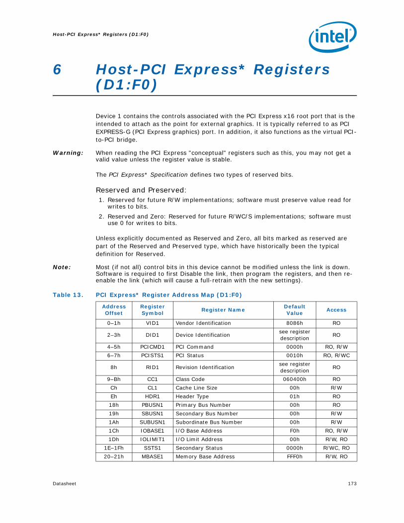
Datasheet 173
Host-PCI Express* Registers (D1:F0)
6 Host-PCI Express* Registers (D1:F0)
Device 1 contains the controls associated with the PCI Express x16 root port that is the intended to attach as the point for external graphics. It is typically referred to as PCI EXPRESS-G (PCI Express graphics) port. In addition, it also functions as the virtual PCI-to-PCI bridge.
Warning: When reading the PCI Express "conceptual" registers such as this, you may not get a valid value unless the register value is stable.
The PCI Express* Specification defines two types of reserved bits.
Reserved and Preserved:1. Reserved for future R/W implementations; software must preserve value read for
writes to bits.
2. Reserved and Zero: Reserved for future R/WC/S implementations; software must use 0 for writes to bits.
Unless explicitly documented as Reserved and Zero, all bits marked as reserved are part of the Reserved and Preserved type, which have historically been the typical definition for Reserved.
Note: Most (if not all) control bits in this device cannot be modified unless the link is down. Software is required to first Disable the link, then program the registers, and then re-enable the link (which will cause a full-retrain with the new settings).
Table 13. PCI Express* Register Address Map (D1:F0)
Address Offset
Register Symbol
Register NameDefault Value
Access
0–1h VID1 Vendor Identification 8086h RO
2–3h DID1 Device Identificationsee register description
RO
4–5h PCICMD1 PCI Command 0000h RO, R/W
6–7h PCISTS1 PCI Status 0010h RO, R/WC
8h RID1 Revision Identificationsee register description
RO
9–Bh CC1 Class Code 060400h RO
Ch CL1 Cache Line Size 00h R/W
Eh HDR1 Header Type 01h RO
18h PBUSN1 Primary Bus Number 00h RO
19h SBUSN1 Secondary Bus Number 00h R/W
1Ah SUBUSN1 Subordinate Bus Number 00h R/W
1Ch IOBASE1 I/O Base Address F0h RO, R/W
1Dh IOLIMIT1 I/O Limit Address 00h R/W, RO
1E–1Fh SSTS1 Secondary Status 0000h R/WC, RO
20–21h MBASE1 Memory Base Address FFF0h R/W, RO

Host-PCI Express* Registers (D1:F0)
174 Datasheet
22–23h MLIMIT1 Memory Limit Address 0000h RO, R/W
24–25h PMBASE1 Prefetchable Memory Base Address FFF1h R/W, RO
26–27h PMLIMIT1 Prefetchable Memory Limit Address 0001h RO, R/W
28–2Bh PMBASEU1Prefetchable Memory Base Address Upper
00000000h R/W
2C–2Fh PMLIMITU1Prefetchable Memory Limit Address Upper
00000000h R/W
34h CAPPTR1 Capabilities Pointer 88h RO
3Ch INTRLINE1 Interrupt Line 00h R/W
3Dh INTRPIN1 Interrupt Pin 01h RO
3E–3Fh BCTRL1 Bridge Control 0000h RO, R/W
80–83h PM_CAPID1 Power Management Capabilities C8039001h RO
84–87h PM_CS1 Power Management Control/Status 00000008hRO, R/W/P,
R/W
88–8Bh SS_CAPIDSubsystem ID and Vendor ID Capabilities
0000800Dh RO
8C–8Fh SSSubsystem ID and Subsystem Vendor ID
00008086h R/WO
90–91h MSI_CAPIDMessage Signaled Interrupts Capability ID
A005h RO
92–93h MC Message Control 0000h RO, R/W
94–97h MA Message Address 00000000h R/W, RO
98–99h MD Message Data 0000h R/W
A0–A1h PEG_CAPL PCI Express-G Capability List 0010h RO
A2–A3h PEG_CAP PCI Express-G Capabilities 0142h RO, R/WO
A4–A7h DCAP Device Capabilities 00008000h RO
A8–A9h DCTL Device Control 0000h RO, R/W
AA–ABh DSTS Device Status 0000h RO, R/WC
AC–AFh LCAP Link Capabilities 02214D02h RO, R/WO
B0–B1h LCTL Link Control 0000hR/W, RO, R/W/SC
B2–B3h LSTS Link Status 1000h R/WC, RO
B4–B7h SLOTCAP Slot Capabilities 00040000h R/WO, RO
B8–B9h SLOTCTL Slot Control 0000h RO, R/W
BA–BBh SLOTSTS Slot Status 0000h RO, R/WC
BC–BDh RCTL Root Control 0000h RO, R/W
C0–C3h RSTS Root Status 00000000h RO, R/WC
EC–EFh PEGLC PCI Express-G Legacy Control 00000000h RO, R/W
Table 13. PCI Express* Register Address Map (D1:F0)
Address Offset
Register Symbol
Register NameDefault Value
Access

Datasheet 175
Host-PCI Express* Registers (D1:F0)
6.1 Host-PCI Express* Register Description (D1:F0)
6.1.1 VID1—Vendor Identification
B/D/F/Type: 0/1/0/PCIAddress Offset: 0-1hDefault Value: 8086hAccess: ROSize: 16 bits
This register, combined with the Device Identification register, uniquely identifies any PCI device.
6.1.2 DID1—Device Identification
B/D/F/Type: 0/1/0/PCIAddress Offset: 2-3hDefault Value: 2E01hAccess: ROSize: 16 bits
This register, combined with the Vendor Identification register, uniquely identifies any PCI device.
Bit AccessDefault Value
RST/PWR Description
15:0 RO 8086h CoreVendor Identification (VID1): PCI standard identification for Intel.
Bit AccessDefault Value
RST/PWR Description
15:8 RO 2Eh CoreDevice Identification Number (DID1(UB)): Identifier assigned to the (G)MCH device 1 (virtual PCI-to-PCI bridge, PCI Express Graphics port).
7:4 RO 0h CoreDevice Identification Number (DID1(HW)): Identifier assigned to the (G)MCH device 1 (virtual PCI-to-PCI bridge, PCI Express Graphics port).
3:0 RO 1h CoreDevice Identification Number (DID1(LB)): Identifier assigned to the (G)MCH device 1 (virtual PCI-to-PCI bridge, PCI Express Graphics port).

Host-PCI Express* Registers (D1:F0)
176 Datasheet
6.1.3 PCICMD1—PCI Command
B/D/F/Type: 0/1/0/PCIAddress Offset: 4-5hDefault Value: 0000hAccess: RO, R/WSize: 16 bits
Bit AccessDefault Value
RST/PWR Description
15:11 RO 00h Core Reserved
10 R/W 0b Core
INTA Assertion Disable (INTAAD):
0 = This device is permitted to generate INTA interrupt messages.
1 = This device is prevented from generating interrupt messages. Any INTA emulation interrupts already asserted must be de-asserted when this bit is set.
Only affects interrupts generated by the device (PCI INTA from a PME or Hot Plug event) controlled by this command register. It does not affect upstream MSIs, upstream PCI INTA–INTD assert and de-assert messages.
9 RO 0b CoreFast Back-to-Back Enable (FB2B): Not Applicable or Implemented. Hardwired to 0.
8 R/W 0b Core
SERR# Message Enable (SERRE1): This bit controls Device 1 SERR# messaging. The (G)MCH communicates the SERR# condition by sending a SERR message to the ICH. This bit, when set, enables reporting of non-fatal and fatal errors detected by the device to the Root Complex. Note that errors are reported if enabled either through this bit or through the PCI-Express specific bits in the Device Control Register.In addition, for Type 1 configuration space header devices, this bit, when set, enables transmission by the primary interface of ERR_NONFATAL and ERR_FATAL error messages forwarded from the secondary interface. This bit does not affect the transmission of forwarded ERR_COR messages.0 = The SERR message is generated by the (G)MCH for
Device 1 only under conditions enabled individually through the Device Control Register.
1 = The (G)MCH is enabled to generate SERR messages, which will be sent to the ICH for specific Device 1 error conditions generated/detected on the primary side of the virtual PCI to PCI bridge (not those received by the secondary side). The status of SERRs generated is reported in the PCISTS1 register.
7 RO 0b Core Reserved: Not Applicable or Implemented. Hardwired to 0.
6 R/W 0b Core
Parity Error Response Enable (PERRE): This bit controls whether or not the Master Data Parity Error bit in the PCI Status register can bet set.0 = Master Data Parity Error bit in PCI Status register can
NOT be set.1 = Master Data Parity Error bit in PCI Status register CAN
be set.

Datasheet 177
Host-PCI Express* Registers (D1:F0)
5 RO 0b CoreVGA Palette Snoop (VGAPS): Not Applicable or Implemented. Hardwired to 0.
4 RO 0b CoreMemory Write and Invalidate Enable (MWIE): Not Applicable or Implemented. Hardwired to 0.
3 RO 0b CoreSpecial Cycle Enable (SCE): Not Applicable or Implemented. Hardwired to 0.
2 R/W 0b Core
Bus Master Enable (BME): This bit controls the ability of the PEG port to forward Memory and IO Read/Write Requests in the upstream direction.0 = This device is prevented from making memory or I/O
requests to its primary bus. Note that according to PCI Specification, as MSI interrupt messages are in-band memory writes, disabling the bus master enable bit prevents this device from generating MSI interrupt messages or passing them from its secondary bus to its primary bus. Upstream memory writes/reads, I/O writes/reads, peer writes/reads, and MSIs will all be treated as invalid cycles. Writes are forwarded to memory address C0000h with byte enables de-asserted. Reads are forwarded to memory address C0000h and will return Unsupported Request status (or Master abort) in its completion packet.
1 = This device is allowed to issue requests to its primary bus. Completions for previously issued memory read requests on the primary bus will be issued when the data is available. This bit does not affect forwarding of Completions from the primary interface to the secondary interface.
1 R/W 0b Core
Memory Access Enable (MAE): 0 = All of device 1's memory space is disabled.1 = Enable the Memory and Pre-fetchable memory
address ranges defined in the MBASE1, MLIMIT1, PMBASE1, and PMLIMIT1 registers.
0 R/W 0b Core
IO Access Enable (IOAE): 0 = All of device 1's I/O space is disabled.1 = Enable the I/O address range defined in the IOBASE1,
and IOLIMIT1 registers.
Bit AccessDefault Value
RST/PWR Description

Host-PCI Express* Registers (D1:F0)
178 Datasheet
6.1.4 PCISTS1—PCI Status
B/D/F/Type: 0/1/0/PCIAddress Offset: 6-7hDefault Value: 0010hAccess: RO, R/WCSize: 16 bits
This register reports the occurrence of error conditions associated with primary side of the "virtual" Host-PCI Express bridge embedded within the (G)MCH.
Bit AccessDefault Value
RST/PWR Description
15 RO 0b Core
Detected Parity Error (DPE): Not Applicable or Implemented. Hardwired to 0. Parity (generating poisoned TLPs) is not supported on the primary side of this device. Error forwarding is not performed.
14 R/WC 0b Core
Signaled System Error (SSE): This bit is set when this Device sends an SERR due to detecting an ERR_FATAL or ERR_NONFATAL condition and the SERR Enable bit in the Command register is 1. Both received (if enabled by BCTRL1[1]) and internally detected error messages do not affect this field.
13 RO 0b CoreReceived Master Abort Status (RMAS): Not Applicable or Implemented. Hardwired to 0. The concept of a master abort does not exist on primary side of this device.
12 RO 0b CoreReceived Target Abort Status (RTAS): Not Applicable or Implemented. Hardwired to 0. The concept of a target abort does not exist on primary side of this device.
11 RO 0b CoreSignaled Target Abort Status (STAS): Not Applicable or Implemented. Hardwired to 0. The concept of a target abort does not exist on primary side of this device.
10:9 RO 00b Core
DEVSELB Timing (DEVT): This device is not the subtractive decode device on bus 0. This bit field is therefore hardwired to 00 to indicate that the device uses the fastest possible decode.
8 RO 0b Core
Master Data Parity Error (PMDPE): Because the primary side of the PEG's virtual PCI-to-PCI bridge is integrated with the MCH functionality there is no scenario where this bit will get set. Because hardware will never set this bit, it is impossible for software to have an opportunity to clear this bit or otherwise test that it is implemented. The PCI specification defines it as a R/WC, but for our implementation an RO definition behaves the same way and will meet all Microsoft testing requirements.This bit can only be set when the Parity Error Enable bit in the PCI Command register is set.
7 RO 0b CoreFast Back-to-Back (FB2B): Not Applicable or Implemented. Hardwired to 0.
6 RO 0b Core Reserved
5 RO 0b Core66/60MHz capability (CAP66): Not Applicable or Implemented. Hardwired to 0.

Datasheet 179
Host-PCI Express* Registers (D1:F0)
6.1.5 RID1—Revision Identification
B/D/F/Type: 0/1/0/PCIAddress Offset: 8hDefault Value: see description belowAccess: ROSize: 8 bits
This register contains the revision number of the (G)MCH device 1. These bits are read only and writes to this register have no effect.
4 RO 1b CoreCapabilities List (CAPL): This bit indicates that a capabilities list is present. Hardwired to 1.
3 RO 0b Core
INTA Status (INTAS): This bit indicates that an interrupt message is pending internally to the device. Only PME and Hot Plug sources feed into this status bit (not PCI INTA-INTD assert and de-assert messages). The INTA Assertion Disable bit, PCICMD1[10], has no effect on this bit.Note that INTA emulation interrupts received across the link are not reflected in this bit.
2:0 RO 000b Core Reserved
Bit AccessDefault Value
RST/PWR Description
Bit AccessDefault Value
RST/PWR Description
7:0 ROsee
descriptionCore
Revision Identification Number (RID1): This is an 8-bit value that indicates the revision identification number for the (G)MCH Device 0. Refer to the Intel® 4 Series Chipset Family Specification Update for the value of this register.

Host-PCI Express* Registers (D1:F0)
180 Datasheet
6.1.6 CC1—Class Code
B/D/F/Type: 0/1/0/PCIAddress Offset: 9-BhDefault Value: 060400hAccess: ROSize: 24 bits
This register identifies the basic function of the device, a more specific sub-class, and a register- specific programming interface.
6.1.7 CL1—Cache Line Size
B/D/F/Type: 0/1/0/PCIAddress Offset: ChDefault Value: 00hAccess: R/WSize: 8 bits
Bit AccessDefault Value
RST/PWR Description
23:16 RO 06h CoreBase Class Code (BCC): This field indicates the base class code for this device. 06h = Bridge device.
15:8 RO 04h CoreSub-Class Code (SUBCC): This field indicates the sub-class code for this device. 04h = PCI-to-PCI Bridge.
7:0 RO 00h Core
Programming Interface (PI): This field indicates the programming interface of this device. This value does not specify a particular register set layout and provides no practical use for this device.
Bit AccessDefault Value
RST/PWR Description
7:0 R/W 00h Core
Cache Line Size (Scratch pad): This field is implemented by PCI Express devices as a read-write field for legacy compatibility purposes but has no impact on any PCI Express device functionality.

Datasheet 181
Host-PCI Express* Registers (D1:F0)
6.1.8 HDR1—Header Type
B/D/F/Type: 0/1/0/PCIAddress Offset: EhDefault Value: 01hAccess: ROSize: 8 bits
This register identifies the header layout of the configuration space. No physical register exists at this location.
6.1.9 PBUSN1—Primary Bus Number
B/D/F/Type: 0/1/0/PCIAddress Offset: 18hDefault Value: 00hAccess: ROSize: 8 bits
This register identifies that this "virtual" Host-PCI Express bridge is connected to PCI bus 0.
6.1.10 SBUSN1—Secondary Bus Number
B/D/F/Type: 0/1/0/PCIAddress Offset: 19hDefault Value: 00hAccess: R/WSize: 8 bits
This register identifies the bus number assigned to the second bus side of the "virtual" bridge (i.e., to PCI Express). This number is programmed by the PCI configuration software to allow mapping of configuration cycles to PCI Express.
Bit AccessDefault Value
RST/PWR Description
7:0 RO 01h CoreHeader Type Register (HDR): This field returns 01h to indicate that this is a single function device with bridge header layout.
Bit AccessDefault Value
RST/PWR Description
7:0 RO 00h Core
Primary Bus Number (BUSN): Configuration software typically programs this field with the number of the bus on the primary side of the bridge. Since device 1 is an internal device and its primary bus is always 0, these bits are read only and are hardwired to 0.
Bit AccessDefault Value
RST/PWR Description
7:0 R/W 00h CoreSecondary Bus Number (BUSN): This field is programmed by configuration software with the bus number assigned to PCI Express.

Host-PCI Express* Registers (D1:F0)
182 Datasheet
6.1.11 SUBUSN1—Subordinate Bus Number
B/D/F/Type: 0/1/0/PCIAddress Offset: 1AhDefault Value: 00hAccess: R/WSize: 8 bits
This register identifies the subordinate bus (if any) that resides at the level below PCI Express. This number is programmed by the PCI configuration software to allow mapping of configuration cycles to PCI Express.
6.1.12 IOBASE1—I/O Base Address
B/D/F/Type: 0/1/0/PCIAddress Offset: 1ChDefault Value: F0hAccess: RO, R/WSize: 8 bits
This register controls the processor to PCI Express I/O access routing based on the following formula:
IO_BASE ≤ address ≤ IO_LIMIT
Only upper 4 bits are programmable. For the purpose of address decode, address bits A[11:0] are treated as 0. Thus, the bottom of the defined I/O address range will be aligned to a 4 KB boundary.
Bit AccessDefault Value
RST/PWR Description
7:0 R/W 00h Core
Subordinate Bus Number (BUSN): This register is programmed by configuration software with the number of the highest subordinate bus that lies behind the device 1 bridge. When only a single PCI device resides on the PCI Express segment, this register will contain the same value as the SBUSN1 register.
Bit Access Default Value
RST/PWR
Description
7:4 R/W Fh Core
I/O Address Base (IOBASE): This field corresponds to A[15:12] of the I/O addresses passed by bridge 1 to PCI Express.BIOS must not set this register to 00h; otherwise, 0CF8h/0CFCh accesses will be forwarded to the PCI Express hierarchy associated with this device.
3:0 RO 0h Core Reserved

Datasheet 183
Host-PCI Express* Registers (D1:F0)
6.1.13 IOLIMIT1—I/O Limit Address
B/D/F/Type: 0/1/0/PCIAddress Offset: 1DhDefault Value: 00hAccess: R/W, ROSize: 8 bits
This register controls the processor-to-PCI Express I/O access routing based on the following formula:
IO_BASE ≤ address ≤ IO_LIMIT
Only upper 4 bits are programmable. For the purpose of address decode, address bits A[11:0] are assumed to be FFFh. Thus, the top of the defined I/O address range will be at the top of a 4 KB aligned address block.
6.1.14 SSTS1—Secondary Status
B/D/F/Type: 0/1/0/PCIAddress Offset: 1E-1FhDefault Value: 0000hAccess: R/WC, ROSize: 16 bits
SSTS1 is a 16-bit status register that reports the occurrence of error conditions associated with secondary side (i.e., PCI Express-G side) of the "virtual" PCI-PCI bridge in the (G)MCH.
Bit AccessDefault Value
RST/PWR Description
7:4 R/W 0h Core
I/O Address Limit (IOLIMIT): This field corresponds to A[15:12] of the I/O address limit of device 1. Devices between this upper limit and IOBASE1 will be passed to the PCI Express hierarchy associated with this device.
3:0 RO 0h Core Reserved
Bit AccessDefault Value
RST/PWR Description
15 R/WC 0b Core
Detected Parity Error (DPE): This bit is set by the Secondary Side for a Type 1 Configuration Space header device whenever it receives a Poisoned TLP, regardless of the state of the Parity Error Response Enable bit in the Bridge Control Register.
14 R/WC 0b CoreReceived System Error (RSE): This bit is set when the Secondary Side for a Type 1 configuration space header device receives an ERR_FATAL or ERR_NONFATAL.
13 R/WC 0b Core
Received Master Abort (RMA): This bit is set when the Secondary Side for Type 1 Configuration Space Header Device (for requests initiated by the Type 1 Header Device itself) receives a Completion with Unsupported Request Completion Status.

Host-PCI Express* Registers (D1:F0)
184 Datasheet
6.1.15 MBASE1—Memory Base Address
B/D/F/Type: 0/1/0/PCIAddress Offset: 20-21hDefault Value: FFF0hAccess: R/W, ROSize: 16 bits
This register controls the processor to PCI Express non-prefetchable memory access routing based on the following formula:
MEMORY_BASE ≤ address ≤ MEMORY_LIMIT
The upper 12 bits of the register are read/write and correspond to the upper 12 address bits A[31:20] of the 32 bit address. The bottom 4 bits of this register are read-only and return zeroes when read. This register must be initialized by the configuration software. For the purpose of address decode, address bits A[19:0] are assumed to be 0. Thus, the bottom of the defined memory address range will be aligned to a 1 MB boundary.
12 R/WC 0b Core
Received Target Abort (RTA): This bit is set when the Secondary Side for Type 1 Configuration Space Header Device (for requests initiated by the Type 1 Header Device itself) receives a Completion with Completer Abort Completion Status.
11 RO 0b Core
Signaled Target Abort (STA): Not Applicable or Implemented. Hardwired to 0. The (G)MCH does not generate Target Aborts (the (G)MCH will never complete a request using the Completer Abort Completion status.
10:9 RO 00b CoreDEVSELB Timing (DEVT): Not Applicable or Implemented. Hardwired to 0.
8 R/WC 0b Core
Master Data Parity Error (SMDPE): When set, this bit indicates that the MCH received across the link (upstream) a Read Data Completion Poisoned TLP (EP=1). This bit can only be set when the Parity Error Enable bit in the Bridge Control register is set.
7 RO 0b CoreFast Back-to-Back (FB2B): Not Applicable or Implemented. Hardwired to 0.
6 RO 0b Core Reserved
5 RO 0b Core66/60 MHz capability (CAP66): Not Applicable or Implemented. Hardwired to 0.
4:0 RO 00h Core Reserved
Bit AccessDefault Value
RST/PWR Description
Bit AccessDefault Value
RST/PWR Description
15:4 R/W FFFh CoreMemory Address Base (MBASE): This field corresponds to A[31:20] of the lower limit of the memory range that will be passed to PCI Express.
3:0 RO 0h Core Reserved

Datasheet 185
Host-PCI Express* Registers (D1:F0)
6.1.16 MLIMIT1—Memory Limit Address
B/D/F/Type: 0/1/0/PCIAddress Offset: 22-23hDefault Value: 0000hAccess: RO, R/WSize: 16 bits
This register controls the processor to PCI Express non-prefetchable memory access routing based on the following formula:
MEMORY_BASE ≤ address ≤ MEMORY_LIMIT
The upper 12 bits of the register are read/write and correspond to the upper 12 address bits A[31:20] of the 32 bit address. The bottom 4 bits of this register are read-only and return zeroes when read. This register must be initialized by the configuration software. For the purpose of address decode, address bits A[19:0] are assumed to be FFFFFh. Thus, the top of the defined memory address range will be at the top of a 1 MB aligned memory block.
Note: Memory range covered by MBASE and MLIMIT registers are used to map non-prefetchable PCI Express address ranges (typically where control/status memory-mapped I/O data structures of the graphics controller will reside) and PMBASE and PMLIMIT are used to map prefetchable address ranges (typically graphics local memory). This segregation allows application of USWC space attribute to be performed in a true plug-and-play manner to the prefetchable address range for improved processor- PCI Express memory access performance.
Note: Configuration software is responsible for programming all address range registers (prefetchable, non-prefetchable) with the values that provide exclusive address ranges i.e. prevent overlap with each other and/or with the ranges covered with the main memory. There is no provision in the (G)MCH hardware to enforce prevention of overlap and operations of the system in the case of overlap are not ensured.
Bit AccessDefault Value
RST/PWR Description
15:4 R/W 000h CoreMemory Address Limit (MLIMIT): This field corresponds to A[31:20] of the upper limit of the address range passed to PCI Express.
3:0 RO 0h Core Reserved

Host-PCI Express* Registers (D1:F0)
186 Datasheet
6.1.17 PMBASE1—Prefetchable Memory Base Address
B/D/F/Type: 0/1/0/PCIAddress Offset: 24-25hDefault Value: FFF1hAccess: R/W, ROSize: 16 bits
This register in conjunction with the corresponding Upper Base Address register controls the processor to PCI Express prefetchable memory access routing based on the following formula:
PREFETCHABLE_MEMORY_BASE ≤ address ≤ PREFETCHABLE_MEMORY_LIMIT
The upper 12 bits of this register are read/write and correspond to address bits A[31:20] of the 40-bit address. The lower 8 bits of the Upper Base Address register are read/write and correspond to address bits A[39:32] of the 40-bit address. This register must be initialized by the configuration software. For the purpose of address decode, address bits A[19:0] are assumed to be 0. Thus, the bottom of the defined memory address range will be aligned to a 1 MB boundary.
Bit AccessDefault Value
RST/PWR Description
15:4 R/W FFFh CorePrefetchable Memory Base Address (MBASE): This field corresponds to A[31:20] of the lower limit of the memory range that will be passed to PCI Express.
3:0 RO 1h Core
64-bit Address Support (64-bit Address Support): This field indicates that the upper 32 bits of the prefetchable memory region base address are contained in the Prefetchable Memory base Upper Address register at 28h.

Datasheet 187
Host-PCI Express* Registers (D1:F0)
6.1.18 PMLIMIT1—Prefetchable Memory Limit Address
B/D/F/Type: 0/1/0/PCIAddress Offset: 26-27hDefault Value: 0001hAccess: RO, R/WSize: 16 bits
This register in conjunction with the corresponding Upper Limit Address register controls the processor to PCI Express prefetchable memory access routing based on the following formula:
PREFETCHABLE_MEMORY_BASE ≤ address ≤ PREFETCHABLE_MEMORY_LIMIT
The upper 12 bits of this register are read/write and correspond to address bits A[31:20] of the 40-bit address. The lower 8 bits of the Upper Limit Address register are read/write and correspond to address bits A[39:32] of the 40-bit address. This register must be initialized by the configuration software. For the purpose of address decode, address bits A[19:0] are assumed to be FFFFFh. Thus, the top of the defined memory address range will be at the top of a 1 MB aligned memory block. Note that prefetchable memory range is supported to allow segregation by the configuration software between the memory ranges that must be defined as UC and the ones that can be designated as a USWC (i.e., prefetchable) from the processor perspective.
Bit Access Default Value
RST/PWR
Description
15:4 R/W 000h Core Prefetchable Memory Address Limit (PMLIMIT): This field corresponds to A[31:20] of the upper limit of the address range passed to PCI Express.
3:0 RO 1h Core 64-bit Address Support (64-bit Address Support): This field indicates that the upper 32 bits of the prefetchable memory region limit address are contained in the Prefetchable Memory Base Limit Address register at 2Ch.

Host-PCI Express* Registers (D1:F0)
188 Datasheet
6.1.19 PMBASEU1—Prefetchable Memory Base Address Upper
B/D/F/Type: 0/1/0/PCIAddress Offset: 28-2BhDefault Value: 00000000hAccess: R/WSize: 32 bits
The functionality associated with this register is present in the PEG design implementation.
This register in conjunction with the corresponding Upper Base Address register controls the processor to PCI Express prefetchable memory access routing based on the following formula:
PREFETCHABLE_MEMORY_BASE ≤ address ≤ PREFETCHABLE_MEMORY_LIMIT
The upper 12 bits of this register are read/write and correspond to address bits A[31:20] of the 40-bit address. The lower 8 bits of the Upper Base Address register are read/write and correspond to address bits A[39:32] of the 40-bit address. This register must be initialized by the configuration software. For the purpose of address decode, address bits A[19:0] are assumed to be 0. Thus, the bottom of the defined memory address range will be aligned to a 1 MB boundary.
Bit AccessDefault Value
RST/PWR Description
31:0 R/W 00000000h Core
Prefetchable Memory Base Address (MBASEU): This field corresponds to A[63:32] of the lower limit of the prefetchable memory range that will be passed to PCI Express.
Datasheet 189
Host-PCI Express* Registers (D1:F0)
6.1.20 PMLIMITU1—Prefetchable Memory Limit Address Upper
B/D/F/Type: 0/1/0/PCIAddress Offset: 2C-2FhDefault Value: 00000000hAccess: R/WSize: 32 bits
The functionality associated with this register is present in the PEG design implementation.
This register in conjunction with the corresponding Upper Limit Address register controls the processor to PCI Express prefetchable memory access routing based on the following formula:
PREFETCHABLE_MEMORY_BASE ≤ address ≤ PREFETCHABLE_MEMORY_LIMIT
The upper 12 bits of this register are read/write and correspond to address bits A[31:20] of the 40- bit address. The lower 8 bits of the Upper Limit Address register are read/write and correspond to address bits A[39:32] of the 40-bit address. This register must be initialized by the configuration software. For the purpose of address decode, address bits A[19:0] are assumed to be FFFFFh. Thus, the top of the defined memory address range will be at the top of a 1 MB aligned memory block.
Note that prefetchable memory range is supported to allow segregation by the configuration software between the memory ranges that must be defined as UC and the ones that can be designated as a USWC (i.e., prefetchable) from the processor perspective.
6.1.21 CAPPTR1—Capabilities Pointer
B/D/F/Type: 0/1/0/PCIAddress Offset: 34hDefault Value: 88hAccess: ROSize: 8 bits
The capabilities pointer provides the address offset to the location of the first entry in this device's linked list of capabilities.
Bit AccessDefault Value
RST/PWR Description
31:0 R/W 00000000h Core
Prefetchable Memory Address Limit (MLIMITU): This field corresponds to A[63:32] of the upper limit of the prefetchable Memory range that will be passed to PCI Express.
Bit AccessDefault Value
RST/PWR Description
7:0 RO 88h CoreFirst Capability (CAPPTR1): The first capability in the list is the Subsystem ID and Subsystem Vendor ID Capability.

Host-PCI Express* Registers (D1:F0)
190 Datasheet
6.1.22 INTRLINE1—Interrupt Line
B/D/F/Type: 0/1/0/PCIAddress Offset: 3ChDefault Value: 00hAccess: R/WSize: 8 bits
This register contains interrupt line routing information. The device itself does not use this value, rather it is used by device drivers and operating systems to determine priority and vector information.
6.1.23 INTRPIN1—Interrupt Pin
B/D/F/Type: 0/1/0/PCIAddress Offset: 3DhDefault Value: 01hAccess: ROSize: 8 bits
This register specifies which interrupt pin this device uses.
Bit AccessDefault Value
RST/PWR Description
7:0 R/W 00h Core
Interrupt Connection (INTCON): This field is used to communicate interrupt line routing information.BIOS Requirement: POST software writes the routing information into this register as it initializes and configures the system. The value indicates to which input of the system interrupt controller this device's interrupt pin is connected.
Bit AccessDefault Value
RST/PWR Description
7:0 RO 01h CoreInterrupt Pin (INTPIN): As a single function device, the PCI Express device specifies INTA as its interrupt pin. 01h=INTA.

Datasheet 191
Host-PCI Express* Registers (D1:F0)
6.1.24 BCTRL1—Bridge Control
B/D/F/Type: 0/1/0/PCIAddress Offset: 3E-3FhDefault Value: 0000hAccess: RO, R/WSize: 16 bits
This register provides extensions to the PCICMD1 register that are specific to PCI-PCI bridges. The BCTRL provides additional control for the secondary interface (i.e., PCI Express) as well as some bits that affect the overall behavior of the "virtual" Host-PCI Express bridge in the (G)MCH (e.g., VGA compatible address ranges mapping).
Bit AccessDefault Value
RST/PWR Description
15:12 RO 0h Core Reserved
11 RO 0b CoreDiscard Timer SERR# Enable (DTSERRE): Not Applicable or Implemented. Hardwired to 0.
10 RO 0b CoreDiscard Timer Status (DTSTS): Not Applicable or Implemented. Hardwired to 0.
9 RO 0b CoreSecondary Discard Timer (SDT): Not Applicable or Implemented. Hardwired to 0.
8 RO 0b CorePrimary Discard Timer (PDT): Not Applicable or Implemented. Hardwired to 0.
7 RO 0b CoreFast Back-to-Back Enable (FB2BEN): Not Applicable or Implemented. Hardwired to 0.
6 R/W 0b Core
Secondary Bus Reset (SRESET): Setting this bit triggers a hot reset on the corresponding PCI Express Port. This will force the LTSSM to transition to the Hot Reset state (via Recovery) from L0 or L1 states.
5 RO 0b CoreMaster Abort Mode (MAMODE): Does not apply to PCI Express. Hardwired to 0.
4 R/W 0b Core
VGA 16-bit Decode (VGA16D): Enables the PCI-to-PCI bridge to provide 16-bit decoding of VGA I/O address precluding the decoding of alias addresses every 1 KB. This bit only has meaning if bit 3 (VGA Enable) of this register is also set to 1, enabling VGA I/O decoding and forwarding by the bridge.0 = Execute 10-bit address decodes on VGA I/O accesses.1 = Execute 16-bit address decodes on VGA I/O accesses.
3 R/W 0b Core
VGA Enable (VGAEN): This bit controls the routing of processor-initiated transactions targeting VGA compatible I/O and memory address ranges. See the VGAEN/MDAP table in device 0, offset 97h[0].

Host-PCI Express* Registers (D1:F0)
192 Datasheet
2 R/W 0b Core
ISA Enable (ISAEN): This bit is needed to exclude legacy resource decode to route ISA resources to legacy decode path. Modifies the response by the (G)MCH to an I/O access issued by the processor that target ISA I/O addresses. This applies only to I/O addresses that are enabled by the IOBASE and IOLIMIT registers.0 = All addresses defined by the IOBASE and IOLIMIT for
processor I/O transactions will be mapped to PCI Express.
1 = (G)MCH will not forward to PCI Express any I/O transactions addressing the last 768 bytes in each 1 KB block even if the addresses are within the range defined by the IOBASE and IOLIMIT registers.
1 R/W 0b Core
SERR Enable (SERREN): 0 = No forwarding of error messages from secondary side
to primary side that could result in an SERR.1 = ERR_COR, ERR_NONFATAL, and ERR_FATAL messages
result in SERR message when individually enabled by the Root Control register.
0 R/W 0b Core
Parity Error Response Enable (PEREN): This bit controls whether or not the Master Data Parity Error bit in the Secondary Status register is set when the MCH receives across the link (upstream) a Read Data Completion Poisoned TLP.0 = Master Data Parity Error bit in Secondary Status
register can NOT be set. 1 = Master Data Parity Error bit in Secondary Status
register CAN be set.
Bit AccessDefault Value
RST/PWR Description

Datasheet 193
Host-PCI Express* Registers (D1:F0)
6.1.25 PM_CAPID1—Power Management Capabilities
B/D/F/Type: 0/1/0/PCIAddress Offset: 80-83hDefault Value: C8039001hAccess: ROSize: 32 bits
Bit AccessDefault Value
RST/PWR Description
31:27 RO 19h Core
PME Support (PMES): This field indicates the power states in which this device may indicate PME wake via PCI Express messaging. D0, D3hot & D3cold. This device is not required to do anything to support D3hot & D3cold, it simply must report that those states are supported. Refer to the PCI Power Management 1.1 Specification for encoding explanation and other power management details.
26 RO 0b CoreD2 Power State Support (D2PSS): Hardwired to 0 to indicate that the D2 power management state is NOT supported.
25 RO 0b CoreD1 Power State Support (D1PSS): Hardwired to 0 to indicate that the D1 power management state is NOT supported.
24:22 RO 000b CoreAuxiliary Current (AUXC): Hardwired to 0 to indicate that there are no 3.3Vaux auxiliary current requirements.
21 RO 0b CoreDevice Specific Initialization (DSI): Hardwired to 0 to indicate that special initialization of this device is NOT required before generic class device driver is to use it.
20 RO 0b Core Auxiliary Power Source (APS): Hardwired to 0.
19 RO 0b CorePME Clock (PMECLK): Hardwired to 0 to indicate this device does NOT support PMEB generation.
18:16 RO 011b CorePCI PM CAP Version (PCIPMCV): A value of 011b indicates that this function complies with revision 1.2 of the PCI Power Management Interface Specification.
15:8 RO 90h Core
Pointer to Next Capability (PNC): This field contains a pointer to the next item in the capabilities list. If MSICH (CAPL[0] @ 7Fh) is 0, then the next item in the capabilities list is the Message Signaled Interrupts (MSI) capability at 90h. If MSICH (CAPL[0] @ 7Fh) is 1, then the next item in the capabilities list is the PCI Express capability at A0h.
7:0 RO 01h CoreCapability ID (CID): Value of 01h identifies this linked list item (capability structure) as being for PCI Power Management registers.

Host-PCI Express* Registers (D1:F0)
194 Datasheet
6.1.26 PM_CS1—Power Management Control/Status
B/D/F/Type: 0/1/0/PCIAddress Offset: 84-87hDefault Value: 00000008hAccess: RO, R/W/P, R/WSize: 32 bits
Bit AccessDefault Value
RST/PWR Description
31:16 RO 0000h Core Reserved: Not Applicable or Implemented. Hardwired to 0.
15 RO 0b CorePME Status (PMESTS): This bit indicates that this device does not support PMEB generation from D3cold.
14:13 RO 00b CoreData Scale (DSCALE): This bit indicates that this device does not support the power management data register.
12:9 RO 0h CoreData Select (DSEL): This bit indicates that this device does not support the power management data register.
8 R/W/P 0b Core
PME Enable (PMEE): This bit indicates that this device does not generate PMEB assertion from any D-state.0 = PMEB generation not possible from any D State1 = PMEB generation enabled from any D StateThe setting of this bit has no effect on hardware.See PM_CAP[15:11]
7:4 RO 0000b Core Reserved
3 RO 1b Core
No Soft Reset (NSR): When set to 1 this bit indicates that the device is transitioning from D3hot to D0 because the power state commands do not perform a internal reset. Configuration context is preserved. Upon transition no additional operating system intervention is required to preserve configuration context beyond writing the power state bits.When clear the devices do not perform an internal reset upon transitioning from D3hot to D0 via software control of the power state bits.Regardless of this bit the devices that transition from a D3hot-to-D0 by a system or bus segment reset will return to the device state D0 unintialized with only PME context preserved if PME is supported and enabled.
2 RO 0b Core Reserved

Datasheet 195
Host-PCI Express* Registers (D1:F0)
6.1.27 SS_CAPID—Subsystem ID and Vendor ID Capabilities
B/D/F/Type: 0/1/0/PCIAddress Offset: 88-8BhDefault Value: 0000800DhAccess: ROSize: 32 bits
This capability is used to uniquely identify the subsystem where the PCI device resides. Because this device is an integrated part of the system and not an add-in device, it is anticipated that this capability will never be used. However, it is necessary because Microsoft will test for its presence.
1:0 R/W 00b Core
Power State (PS): This field indicates the current power state of this device and can be used to set the device into a new power state. If software attempts to write an unsupported state to this field, write operation must complete normally on the bus, but the data is discarded and no state change occurs.00 = D001 = D1 (Not supported)10 = D2 (Not supported)11 = D3Support of D3cold does not require any special action. While in the D3hot state, this device can only act as the target of PCI configuration transactions (for power management control). This device also cannot generate interrupts or respond to MMR cycles in the D3 state. The device must return to the D0 state in order to be fully-functional.When the Power State is other than D0, the bridge will Master Abort (i.e. not claim) any downstream cycles (with exception of type 0 config cycles). Consequently, these unclaimed cycles will go down DMI and come back up as Unsupported Requests, which the MCH logs as Master Aborts in Device 0 PCISTS[13]There is no additional hardware functionality required to support these Power States.
Bit AccessDefault Value
RST/PWR Description
Bit AccessDefault Value
RST/PWR Description
31:16 RO 0000h Core Reserved
15:8 RO 80h CorePointer to Next Capability (PNC): This field contains a pointer to the next item in the capabilities list which is the PCI Power Management capability.
7:0 RO 0Dh CoreCapability ID (CID): Value of 0Dh identifies this linked list item (capability structure) as being for SSID/SSVID registers in a PCI-to-PCI Bridge.

Host-PCI Express* Registers (D1:F0)
196 Datasheet
6.1.28 SS—Subsystem ID and Subsystem Vendor ID
B/D/F/Type: 0/1/0/PCIAddress Offset: 8C-8FhDefault Value: 00008086hAccess: R/WOSize: 32 bits
System BIOS can be used as the mechanism for loading the SSID/SVID values. These values must be preserved through power management transitions and a hardware reset.
6.1.29 MSI_CAPID—Message Signaled Interrupts Capability ID
B/D/F/Type: 0/1/0/PCIAddress Offset: 90-91hDefault Value: A005hAccess: ROSize: 16 bits
When a device supports MSI, it can generate an interrupt request to the processor by writing a predefined data item (a message) to a predefined memory address.
The reporting of the existence of this capability can be disabled by setting MSICH (CAPL[0] @ 7Fh). In that case walking this linked list will skip this capability and instead go directly from the PCI PM capability to the PCI Express capability.
Bit AccessDefault Value
RST/PWR Description
31:16 R/WO 0000h CoreSubsystem ID (SSID): This field identifies the particular subsystem and is assigned by the vendor.
15:0 R/WO 8086h Core
Subsystem Vendor ID (SSVID): This field identifies the manufacturer of the subsystem and is the same as the vendor ID which is assigned by the PCI Special Interest Group.
Bit AccessDefault Value
RST/PWR Description
15:8 RO A0h CorePointer to Next Capability (PNC): This field contains a pointer to the next item in the capabilities list which is the PCI Express capability.
7:0 RO 05h CoreCapability ID (CID): Value of 05h identifies this linked list item (capability structure) as being for MSI registers.

Datasheet 197
Host-PCI Express* Registers (D1:F0)
6.1.30 MC—Message Control
B/D/F/Type: 0/1/0/PCIAddress Offset: 92-93hDefault Value: 0000hAccess: RO, R/WSize: 16 bits
System software can modify bits in this register, but the device is prohibited from modifying bits.
If the device writes the same message multiple times, only one of those messages is ensured to be serviced. If all of them must be serviced, the device must not generate the same message again until the driver services the earlier one.
Bit AccessDefault Value
RST/PWR Description
15:8 RO 00h Core Reserved
7 RO 0b Core
64-bit Address Capable (64AC): Hardwired to 0 to indicate that the function does not implement the upper 32 bits of the Message Address register and is incapable of generating a 64-bit memory address.This may need to change in future implementations when addressable system memory exceeds the 32b/4 GB limit.
6:4 R/W 000b Core
Multiple Message Enable (MME): System software programs this field to indicate the actual number of messages allocated to this device. This number will be equal to or less than the number actually requested.The encoding is the same as for the MMC field below.
3:1 RO 000b Core
Multiple Message Capable (MMC): System software reads this field to determine the number of messages being requested by this device.000 = 1All other encodings are reserved.
0 R/W 0b Core
MSI Enable (MSIEN): This bit controls the ability of this device to generate MSIs. 0 = MSI will not be generated. 1 = MSI will be generated when we receive PME or
HotPlug messages. INTA will not be generated and INTA Status (PCISTS1[3]) will not be set.
Host-PCI Express* Registers (D1:F0)
198 Datasheet
6.1.31 MA—Message AddressB/D/F/Type: 0/1/0/PCIAddress Offset: 94-97hDefault Value: 00000000hAccess: R/W, ROSize: 32 bits
6.1.32 MD—Message DataB/D/F/Type: 0/1/0/PCIAddress Offset: 98-99hDefault Value: 0000hAccess: R/WSize: 16 bits
6.1.33 PEG_CAPL—PCI Express-G Capability ListB/D/F/Type: 0/1/0/PCIAddress Offset: A0-A1hDefault Value: 0010hAccess: ROSize: 16 bits
This register enumerates the PCI Express capability structure.
Bit AccessDefault Value
RST/PWR Description
31:2 R/W 00000000h Core
Message Address (MA): This field is used by system software to assign an MSI address to the device. The device handles an MSI by writing the padded contents of the MD register to this address.
1:0 RO 00b CoreForce DWord Align (FDWA): Hardwired to 0 so that addresses assigned by system software are always aligned on a dword address boundary.
Bit AccessDefault Value
RST/PWR Description
15:0 R/W 0000h Core
Message Data (MD): This field is the base message data pattern assigned by system software and used to handle an MSI from the device.When the device must generate an interrupt request, it writes a 32-bit value to the memory address specified in the MA register. The upper 16 bits are always set to 0. The lower 16 bits are supplied by this register.
Bit AccessDefault Value
RST/PWR Description
15:8 RO 00h Core
Pointer to Next Capability (PNC): This value terminates the capabilities list. The Virtual Channel capability and any other PCI Express specific capabilities that are reported via this mechanism are in a separate capabilities list located entirely within PCI Express Extended Configuration Space.
7:0 RO 10h CoreCapability ID (CID): This field identifies this linked list item (capability structure) as being for PCI Express registers.

Datasheet 199
Host-PCI Express* Registers (D1:F0)
6.1.34 PEG_CAP—PCI Express-G CapabilitiesB/D/F/Type: 0/1/0/PCIAddress Offset: A2-A3hDefault Value: 0142hAccess: RO, R/WOSize: 16 bits
This register indicates PCI Express device capabilities.
6.1.35 DCAP—Device CapabilitiesB/D/F/Type: 0/1/0/PCIAddress Offset: A4-A7hDefault Value: 00008000hAccess: ROSize: 32 bits
This register indicates PCI Express device capabilities.
Bit AccessDefault Value
RST/PWR Description
15:14 RO 0b Core Reserved
13:9 RO 00h CoreInterrupt Message Number (IMN): Not Applicable or Implemented. Hardwired to 0.
8 R/WO 1b Core
Slot Implemented (SI):0 = The PCI Express Link associated with this port is
connected to an integrated component or is disabled.1 = The PCI Express Link associated with this port is
connected to a slot.BIOS Requirement: This field must be initialized appropriately if a slot connection is not implemented.
7:4 RO 4h CoreDevice/Port Type (DPT): Hardwired to 4h to indicate root port of PCI Express Root Complex.
3:0 RO 2h CorePCI Express Capability Version (PCIECV): Hardwired to 2h to indicate compliance to the PCI Express Capabilities Register Expansion ECN.
Bit AccessDefault Value
RST/PWR Description
31:16 RO 0000h Core Reserved: Not Applicable or Implemented. Hardwired to 0.
15 RO 1b Core
Role Based Error Reporting (RBER): This bit indicates that this device implements the functionality defined in the Error Reporting ECN as required by the PCI Express 1.1 Specification.
14:6 RO 000h Core Reserved: Not Applicable or Implemented. Hardwired to 0.
5 RO 0b CoreExtended Tag Field Supported (ETFS): Hardwired to indicate support for 5-bit Tags as a Requestor.
4:3 RO 00b CorePhantom Functions Supported (PFS): Not Applicable or Implemented. Hardwired to 0.
2:0 RO 000b CoreMax Payload Size (MPS): Hardwired to indicate 128B max supported payload for Transaction Layer Packets (TLP).
Host-PCI Express* Registers (D1:F0)
200 Datasheet
6.1.36 DCTL—Device Control
B/D/F/Type: 0/1/0/PCIAddress Offset: A8-A9hDefault Value: 0000hAccess: RO, R/WSize: 16 bits
This register provides control for PCI Express device specific capabilities.
The error reporting enable bits are in reference to errors detected by this device, not error messages received across the link. The reporting of error messages (ERR_CORR, ERR_NONFATAL, ERR_FATAL) received by Root Port is controlled exclusively by Root Port Command Register.
Bit AccessDefault Value
RST/PWR Description
15:8 RO 0s Core Reserved
7:5 R/W 000b Core
Max Payload Size (MPS):000 = 128B max supported payload for Transaction Layer
Packets (TLP). As a receiver, the Device must handle TLPs as large as the set value, as transmitter, the Device must not generate TLPs exceeding the set value.
All other encodings are reserved.Hardware will actually ignore this field. It is writeable only to support compliance testing.
4 RO 0b Core Reserved for Enable Relaxed Ordering
3 R/W 0b Core
Unsupported Request Reporting Enable (URRE): Unsupported Request Reporting Enable (URRE): When set, this bit allows signaling ERR_NONFATAL, ERR_FATAL, or ERR_CORR to the Root Control register when detecting an unmasked Unsupported Request (UR). An ERR_CORR is signaled when an unmasked Advisory Non-Fatal UR is received. An ERR_FATAL or ERR_NONFATAL is sent to the Root Control register when an uncorrectable non-Advisory UR is received with the severity bit set in the Uncorrectable Error Severity register.
2 R/W 0b Core
Fatal Error Reporting Enable (FERE): Fatal Error Reporting Enable (FERE): When set, enables signaling of ERR_FATAL to the Root Control register due to internally detected errors or error messages received across the link. Other bits also control the full scope of related error reporting.
1 R/W 0b Core
Non-Fatal Error Reporting Enable (NERE): Non-Fatal Error Reporting Enable (NERE): When set, enables signaling of ERR_NONFATAL to the Rool Control register due to internally detected errors or error messages received across the link. Other bits also control the full scope of related error reporting.
0 R/W 0b Core
Correctable Error Reporting Enable (CERE): Correctable Error Reporting Enable (CERE): When set, this bit enables signaling of ERR_CORR to the Root Control register due to internally detected errors or error messages received across the link. Other bits also control the full scope of related error reporting.

Datasheet 201
Host-PCI Express* Registers (D1:F0)
6.1.37 DSTS—Device Status
B/D/F/Type: 0/1/0/PCIAddress Offset: AA-ABhDefault Value: 0000hAccess: RO, R/WCSize: 16 bits
This register reflects status corresponding to controls in the Device Control register. The error reporting bits are in reference to errors detected by this device, not errors messages received across the link.
Bit AccessDefault Value
RST/PWR Description
15:6 RO 000h CoreReserved and Zero: For future R/WC/S implementations; software must use 0 for writes to bits.
5 RO 0b Core
Transactions Pending (TP):0 = All pending transactions (including completions for
any outstanding non-posted requests on any used virtual channel) have been completed.
1 = Indicates that the device has transaction(s) pending (including completions for any outstanding non-posted requests for all used Traffic Classes).
4 RO 0b Core Reserved
3 R/WC 0b Core
Unsupported Request Detected (URD): When set, this bit indicates that the Device received an Unsupported Request. Errors are logged in this register regardless of whether error reporting is enabled or not in the Device Control Register.Additionally, the Non-Fatal Error Detected bit or the Fatal Error Detected bit is set according to the setting of the Unsupported Request Error Severity bit. In production systems setting the Fatal Error Detected bit is not an option as support for AER will not be reported.
2 R/WC 0b Core
Fatal Error Detected (FED): When set, this bit indicates that fatal error(s) were detected. Errors are logged in this register regardless of whether error reporting is enabled or not in the Device Control register. When Advanced Error Handling is enabled, errors are logged in this register regardless of the settings of the uncorrectable error mask register.
1 R/WC 0b Core
Non-Fatal Error Detected (NFED): When set, this bit indicates that non-fatal error(s) were detected. Errors are logged in this register regardless of whether error reporting is enabled or not in the Device Control register.When Advanced Error Handling is enabled, errors are logged in this register regardless of the settings of the uncorrectable error mask register.
0 R/WC 0b Core
Correctable Error Detected (CED): When set, this bit indicates that correctable error(s) were detected. Errors are logged in this register regardless of whether error reporting is enabled or not in the Device Control register.When Advanced Error Handling is enabled, errors are logged in this register regardless of the settings of the correctable error mask register.

Host-PCI Express* Registers (D1:F0)
202 Datasheet
6.1.38 LCAP—Link Capabilities
B/D/F/Type: 0/1/0/PCIAddress Offset: AC-AFhDefault Value: 02214D02hAccess: RO, R/WOSize: 32 bits
This register indicates PCI Express device specific capabilities.
Bit AccessDefault Value
RST/PWR Description
31:24 RO 02h CorePort Number (PN): This field indicates the PCI Express port number for the given PCI Express link. This field matches the value in Element Self Description[31:24].
23:22 RO 00b Core Reserved
21 RO 1b Core
Link Bandwidth Notification Capability (LBNC): A value of 1b indicates support for the Link Bandwidth Notification status and interrupt mechanisms. This capability is required for all Root Ports and Switch downstream ports supporting Links wider than x1 and/or multiple Link speeds.This field is not applicable and is reserved for Endpoint devices, PCI Express to PCI/PCI-X bridges, and Upstream Ports of Switches.Devices that do not implement the Link Bandwidth Notification capability must hardwire this bit to 0b.
20 RO 0b Core
Data Link Layer Link Active Reporting Capable (DLLLARC): For a Downstream Port, this bit must be set to 1b if the component supports the optional capability of reporting the DL_Active state of the Data Link Control and Management State Machine. For a hot-plug capable Downstream Port (as indicated by the Hot-Plug Capable field of the Slot Capabilities register), this bit must be set to 1b.For Upstream Ports and components that do not support this optional capability, this bit must be hardwired to 0b.
19 RO 0b Core
Surprise Down Error Reporting Capable (SDERC): For a Downstream Port, this bit must be set to 1b if the component supports the optional capability of detecting and reporting a Surprise Down error condition.For Upstream Ports and components that do not support this optional capability, this bit must be hardwired to 0b.

Datasheet 203
Host-PCI Express* Registers (D1:F0)
18 RO 0b Core
Clock Power Management (CPM): A value of 1b in this bit indicates that the component tolerates the removal of any reference clock(s) when the link is in the L1 and L2/3 Ready link states. A value of 0b indicates the component does not have this capability and that reference clock(s) must not be removed in these link states.This capability is applicable only in form factors that support "clock request" (CLKREQ#) capability.For a multi-function device, each function indicates its capability independently. Power Management configuration software must only permit reference clock removal if all functions of the multifunction device indicate a 1b in this bit.
17:15 R/WO 010b Core
L1 Exit Latency (L1ELAT): This field indicates the length of time this Port requires to complete the transition from L1 to L0. The value 010 b indicates the range of 2 us to less than 4 us.BIOS Requirement: If this field is required to be any value other than the default, BIOS must initialize it accordingly.Both bytes of this register that contain a portion of this field must be written simultaneously in order to prevent an intermediate (and undesired) value from ever existing.
14:12 RO 100b Core Reserved
11:10 R/WO 11b CoreActive State Link PM Support (ASLPMS): The (G)MCH supports ASPM L1.
9:4 R/WO 10h CoreMax Link Width (MLW): This field indicates the maximum number of lanes supported for this link.
3:0 R/WO 2h Core
Max Link Speed (MLS): Supported Link Speed – This field indicates the supported Link speed(s) of the associated Port. Defined encodings are:0001b = 2.5 GT/s Link speed supported0010b = 5.0 GT/s and 2.5GT/s Link speeds supportedAll other encodings are reserved.
Bit AccessDefault Value
RST/PWR Description

Host-PCI Express* Registers (D1:F0)
204 Datasheet
6.1.39 LCTL—Link Control
B/D/F/Type: 0/1/0/PCIAddress Offset: B0-B1hDefault Value: 0000hAccess: R/W, RO, R/W/SCSize: 16 bits
This register allows control of PCI Express link.
Bit AccessDefault Value
RST/PWR Description
15:12 RO 0000b Core Reserved
11 R/W 0b Core
Link Autonomous Bandwidth Interrupt Enable (LABIE): When Set, this bit enables the generation of an interrupt to indicate that the Link Autonomous Bandwidth Status bit has been Set.This bit is not applicable and is reserved for Endpoint devices, PCI Express to PCI/PCI-X bridges, and Upstream Ports of Switches.Devices that do not implement the Link Bandwidth Notification capability must hardwire this bit to 0b.
10 R/W 0b Core
Link Bandwidth Management Interrupt Enable (LBMIE): When Set, this bit enables the generation of an interrupt to indicate that the Link Bandwidth Management Status bit has been Set.This bit is not applicable and is reserved for Endpoint devices, PCI Express to PCI/PCI-X bridges, and Upstream Ports of Switches.
9 RO 0b Core
Hardware Autonomous Width Disable (HAWD): When Set, this bit disables hardware from changing the Link width for reasons other than attempting to correct unreliable Link operation by reducing Link width.Devices that do not implement the ability autonomously to change Link width are permitted to hardwire this bit to 0b.
8 RO 0b Core
Enable Clock Power Management (ECPM): Applicable only for form factors that support a "Clock Request" (CLKREQ#) mechanism, this enable functions as follows:0 = Clock power management is disabled and device must
hold CLKREQ# signal low1 = When this bit is set to 1, the device is permitted to use
CLKREQ# signal to power manage link clock according to protocol defined in appropriate form factor specification.
Components that do not support Clock Power Management (as indicated by a 0b value in the Clock Power Management bit of the Link Capabilities Register) must hardwire this bit to 0b.
7 R/W 0b Core Reserved

Datasheet 205
Host-PCI Express* Registers (D1:F0)
6 R/W 0b Core
Common Clock Configuration (CCC):0 = Indicates that this component and the component at
the opposite end of this Link are operating with asynchronous reference clock.
1 = Indicates that this component and the component at the opposite end of this Link are operating with a distributed common reference clock.
The state of this bit affects the N_FTS value advertised during link training.See PEGL0SLAT at offset 22Ch.
5 R/W/SC 0b Core
Retrain Link (RL): 0 = Normal operation. 1 = Full Link retraining is initiated by directing the Physical
Layer LTSSM from L0 or L1 states to the Recovery state.
This bit always returns 0 when read. This bit is cleared automatically (no need to write a 0).
4 R/W 0b Core
Link Disable (LD):0 = Normal operation1 = Link is disabled. Forces the LTSSM to transition to the
Disabled state (via Recovery) from L0 or L1 states. Link retraining happens automatically on 0 to 1 transition, just like when coming out of reset.
Writes to this bit are immediately reflected in the value read from the bit, regardless of actual Link state.
3 RO 0b CoreRead Completion Boundary (RCB): Hardwired to 0 to indicate 64 byte.
2 RO 0b Core Reserved
1:0 R/W 00b Core
Active State PM (ASPM): This field controls the level of active state power management supported on the given link.00 = Disabled01 = Reserved10 = L1 Entry Enabled11 = L1 Entry Enabled
Bit AccessDefault Value
RST/PWR Description

Host-PCI Express* Registers (D1:F0)
206 Datasheet
6.1.40 LSTS—Link Status
B/D/F/Type: 0/1/0/PCIAddress Offset: B2-B3hDefault Value: 1000hAccess: R/WC, ROSize: 16 bits
This register indicates PCI Express link status.
Bit AccessDefault Value
RST/PWR Description
15 R/WC 0b Core
Link Autonomous Bandwidth Status (LABWS): This bit is set to 1b by hardware to indicate that hardware has autonomously changed link speed or width, without the port transitioning through DL_Down status, for reasons other than to attempt to correct unreliable link operation.This bit must be set if the Physical Layer reports a speed or width change was initiated by the downstream component that was indicated as an autonomous change.This bit must be set when the upstream component receives eight consecutive TS1 or TS2 ordered sets with the Autonomous Change bit set.
14 R/WC 0b Core
Link Bandwidth Management Status (LBWMS): This bit is set to 1b by hardware to indicate that either of the following has occurred without the port transitioning through DL_Down status:• A link retraining initiated by a write of 1b to the Retrain
Link bit has completed.Note: This bit is Set following any write of 1b to the Retrain Link bit, including when the Link is in the process of retraining for some other reason.
• Hardware has autonomously changed link speed or width to attempt to correct unreliable link operation, either through an LTSSM timeout or a higher level process
This bit must be set if the Physical Layer reports a speed or width change was initiated by the downstream component that was not indicated as an autonomous change.
13 RO 0b Core
Data Link Layer Link Active (Optional) (DLLLA): This bit indicates the status of the Data Link Control and Management State Machine. It returns a 1b to indicate the DL_Active state, 0b otherwise.This bit must be implemented if the corresponding Data Link Layer Active Capability bit is implemented. Otherwise, this bit must be hardwired to 0b.
12 RO 1b Core
Slot Clock Configuration (SCC): 0 = The device uses an independent clock irrespective of
the presence of a reference on the connector.1 = The device uses the same physical reference clock that
the platform provides on the connector.

Datasheet 207
Host-PCI Express* Registers (D1:F0)
11 RO 0b Core
Link Training (LTRN): This bit indicates that the Physical Layer LTSSM is in the Configuration or Recovery state, or that 1b was written to the Retrain Link bit but Link training has not yet begun. Hardware clears this bit when the LTSSM exits the Configuration/Recovery state once Link training is complete.
10 RO 0b Core
Undefined (Undefined): The value read from this bit is undefined. In previous versions of this specification, this bit was used to indicate a Link Training Error. System software must ignore the value read from this bit. System software is permitted to write any value to this bit.
9:4 RO 00h Core
Negotiated Link Width (NLW): This field indicates negotiated link width. This field is valid only when the link is in the L0 or L1 states (after link width negotiation is successfully completed).00h = Reserved01h = X102h = X204h = X408h = X810h = X16All other encodings are reserved.
3:0 RO 0h Core
Current Link Speed (CLS): This field indicates the negotiated Link speed of the given PCI Express Link.0001b = 2.5 GT/s PCI Express Link0010b = 5 GT/s PCI Express LinkAll other encodings are reserved. The value in this field is undefined when the Link is not up.
Bit AccessDefault Value
RST/PWR Description

Host-PCI Express* Registers (D1:F0)
208 Datasheet
6.1.41 SLOTCAP—Slot Capabilities
B/D/F/Type: 0/1/0/PCIAddress Offset: B4-B7hDefault Value: 00040000hAccess: R/WO, ROSize: 32 bits
PCI Express Slot related registers allow for the support of Hot Plug.
Bit AccessDefault Value
RST/PWR Description
31:19 R/WO 0000h Core
Physical Slot Number (PSN): This field indicates the physical slot number attached to this Port.BIOS Requirement: This field must be initialized by BIOS to a value that assigns a slot number that is globally unique within the chassis.
18 R/WO 1b Core
No Command Completed Support (NCCS): When set to 1b, this bit indicates that this slot does not generate software notification when an issued command is completed by the Hot-Plug Controller. This bit is only permitted to be set to 1b if the hotplug capable port is able to accept writes to all fields of the Slot Control register without delay between successive writes.
17 RO 0b Core Reserved
16:15 R/WO 00b Core
Slot Power Limit Scale (SPLS): This field specifies the scale used for the Slot Power Limit Value.00 = 1.0x01 = 0.1x10 = 0.01x11 = 0.001xIf this field is written, the link sends a Set_Slot_Power_Limit message.
14:7 R/WO 00h Core
Slot Power Limit Value (SPLV): In combination with the Slot Power Limit Scale value, this field specifies the upper limit on power supplied by slot. Power limit (in Watts) is calculated by multiplying the value in this field by the value in the Slot Power Limit Scale field.If this field is written, the link sends a Set_Slot_Power_Limit message.
6:0 RO 0b Core Reserved
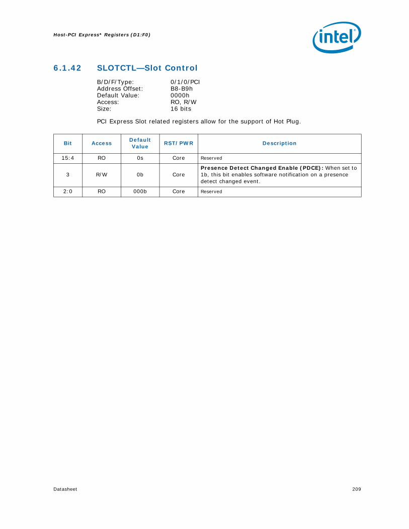
Datasheet 209
Host-PCI Express* Registers (D1:F0)
6.1.42 SLOTCTL—Slot Control
B/D/F/Type: 0/1/0/PCIAddress Offset: B8-B9hDefault Value: 0000hAccess: RO, R/WSize: 16 bits
PCI Express Slot related registers allow for the support of Hot Plug.
Bit AccessDefault Value
RST/PWR Description
15:4 RO 0s Core Reserved
3 R/W 0b CorePresence Detect Changed Enable (PDCE): When set to 1b, this bit enables software notification on a presence detect changed event.
2:0 RO 000b Core Reserved

Host-PCI Express* Registers (D1:F0)
210 Datasheet
6.1.43 SLOTSTS—Slot Status
B/D/F/Type: 0/1/0/PCIAddress Offset: BA-BBhDefault Value: 0000hAccess: RO, R/WCSize: 16 bits
PCI Express Slot related registers allow for the support of Hot Plug.
Bit Access Default Value
RST/PWR
Description
15:9 RO 0000000b CoreReserved and Zero: For future R/WC/S implementations; software must use 0 for writes to bits.
8:7 RO 00b Core Reserved
6 RO 0b Core
Presence Detect State (PDS): In band presence detect state:0 = Slot Empty1 = Card present in slotThis bit indicates the presence of an adapter in the slot, reflected by the logical "OR" of the Physical Layer in-band presence detect mechanism and, if present, any out-of-band presence detect mechanism defined for the slot's corresponding form factor. Note that the in-band presence detect mechanism requires that power be applied to an adapter for its presence to be detected. Consequently, form factors that require a power controller for hot-plug must implement a physical pin presence detect mechanism.This bit must be implemented on all Downstream Ports that implement slots. For Downstream Ports not connected to slots (where the Slot Implemented bit of the PCI Express Capabilities Register is 0b), this bit must return 1b.
5:4 RO 00b Core Reserved
3 R/WC 0b Core
Presence Detect Changed (PDC): A pulse indication that the inband presence detect state has changed. This bit is set when the value reported in Presence Detect State is changed.
2:0 RO 000b Core Reserved

Datasheet 211
Host-PCI Express* Registers (D1:F0)
6.1.44 RCTL—Root Control
B/D/F/Type: 0/1/0/PCIAddress Offset: BC-BDhDefault Value: 0000hAccess: RO, R/WSize: 16 bits
This register allows control of PCI Express Root Complex specific parameters. The system error control bits in this register determine if corresponding SERRs are generated when our device detects an error (reported in this device's Device Status register) or when an error message is received across the link. Reporting of SERR as controlled by these bits takes precedence over the SERR Enable in the PCI Command Register.
Bit AccessDefault Value
RST/PWR Description
15:4 RO 0s Core Reserved
3 R/W 0b Core
PME Interrupt Enable (PMEIE): 0 = No interrupts are generated as a result of receiving
PME messages.
1 = Enables interrupt generation upon receipt of a PME message as reflected in the PME Status bit of the Root Status Register. A PME interrupt is also generated if the PME Status bit of the Root Status Register is set when this bit is set from a cleared state.
2 R/W 0b Core
System Error on Fatal Error Enable (SEFEE): This bit controls the Root Complex's response to fatal errors.0 = No SERR generated on receipt of fatal error.1 = Indicates that an SERR should be generated if a fatal
error is reported by any of the devices in the hierarchy associated with this Root Port, or by the Root Port itself.
1 R/W 0b Core
System Error on Non-Fatal Uncorrectable Error Enable (SENFUEE): This bit controls the Root Complex's response to non-fatal errors.0 = No SERR generated on receipt of non-fatal error.1 = Indicates that an SERR should be generated if a non-
fatal error is reported by any of the devices in the hierarchy associated with this Root Port, or by the Root Port itself.
0 R/W 0b Core
System Error on Correctable Error Enable (SECEE): This bit controls the Root Complex's response to correctable errors.0 = No SERR generated on receipt of correctable error.1 = Indicates that an SERR should be generated if a
correctable error is reported by any of the devices in the hierarchy associated with this Root Port, or by the Root Port itself.

Host-PCI Express* Registers (D1:F0)
212 Datasheet
6.1.45 RSTS—Root Status
B/D/F/Type: 0/1/0/PCIAddress Offset: C0-C3hDefault Value: 00000000hAccess: RO, R/WCSize: 32 bits
This register provides information about PCI Express Root Complex specific parameters.
6.1.46 DCAP2—Device Capabilities 2
B/D/F/Type: 0/1/0/PCIAddress Offset: C4-C7hDefault Value: 00000000hAccess: ROSize: 32 bits
6.1.47 DCTL2—Device Control 2
B/D/F/Type: 0/1/0/PCIAddress Offset: C8-C9hDefault Value: 0000hAccess: ROSize: 16 bits
Bit AccessDefault Value
RST/PWR Description
31:18 RO 0000h CoreReserved and Zero: For future R/WC/S implementations; software must use 0 for writes to bits.
17 RO 0b Core
PME Pending (PMEP): This bit indicates that another PME is pending when the PME Status bit is set. When the PME Status bit is cleared by software; the PME is delivered by hardware by setting the PME Status bit again and updating the Requestor ID appropriately. The PME pending bit is cleared by hardware if no more PMEs are pending.
16 R/WC 0b Core
PME Status (PMES): This bit indicates that PME was asserted by the requestor ID indicated in the PME Requestor ID field. Subsequent PMEs are kept pending until the status register is cleared by writing a 1 to this field.
15:0 RO 0000h CorePME Requestor ID (PMERID): This field indicates the PCI requestor ID of the last PME requestor.
Bit AccessDefault Value
RST/PWR Description
31:0 RO 00000000h Core Reserved
Bit AccessDefault Value
RST/PWR Description
15:0 RO 0000h Core Reserved

Datasheet 213
Host-PCI Express* Registers (D1:F0)
6.1.48 DSTS2—Device Status 2
B/D/F/Type: 0/1/0/PCIAddress Offset: CA-CBhDefault Value: 0000hAccess: ROSize: 16 bits
6.1.49 LCAP2—Link Capabilities 2
B/D/F/Type: 0/1/0/PCIAddress Offset: CC-CFhDefault Value: 00000000hAccess: ROSize: 32 bits
Bit AccessDefault Value
RST/PWR Description
15:0 RO 0000h Core Reserved
Bit AccessDefault Value
RST/PWR Description
31:0 RO 00000000h Core Reserved

Host-PCI Express* Registers (D1:F0)
214 Datasheet
6.1.50 LCTL2—Link Control 2
B/D/F/Type: 0/1/0/PCIAddress Offset: D0-D1hDefault Value: 0002hAccess: R/W/P, R/W, ROSize: 16 bits
Bit AccessDefault Value
RST/PWR Description
15:13 RO 000b Core Reserved
12 R/W/P 0b Core
Compliance De-emphasis: This bit sets the de-emphasis level in Polling.Compliance state if the entry occurred due to the Enter Compliance bit being 1b.1 = 3.5 dB0 = 6 dBWhen the Link is operating at 2.5 GT/s, the setting of this bit has no effect. Components that support only 2.5 GT/s speed are permitted to hardwire this bit to 0b.For a Multi-Function device associated with an Upstream Port, the bit in Function 0 is of type R/WS, and only Function 0 controls the component's Link behavior. In all other Functions of that device, this bit is of type RSVD.This bit is intended for debug, compliance testing purposes.System firmware and software is allowed to modify this bit only during debug or compliance testing.
11 R/W/P 0b Core
Compliance SOS (compsos): When set to 1b, the LTSSM is required to send SKP Ordered Sets periodically in between the (modified) compliance patterns.For a Multi-Function device associated with an Upstream Port, the bit in Function 0 is of type R/WS, and only Function 0 controls the component's Link behavior. In all other Functions of that device, this bit is of type RSVD.Components that support only the 2.5 GT/s speed are permitted to hardwire this field to 0b.
10 R/W/P 0b Core
Enter Modified Compliance (entermodcompliance): When this bit is set to 1b, the device transmits modified compliance pattern if the LTSSM enters Polling.Compliance state.Components that support only the 2.5GT/s speed are permitted to hardwire this bit to 0b.

Datasheet 215
Host-PCI Express* Registers (D1:F0)
9:7 R/W/P 000b Core
Transmit Margin (txmargin): This field controls the value of the non-deemphasized voltage level at the Transmitter pins. This field is reset to 000b on entry to the LTSSM Polling.Configuration substates.000 = Normal operating range001 = 800–1200 mV for full swing and 400–700
mV for half-swing010 – (n-1) = Values must be monotonic with a non-
zero slope. The value of n must be greater than 3 and less than 7. At least two of these must be below the normal operating range
n = 200–400 mV for full-swing and 100–200 mV for half-swing
n – 111 = reservedComponents that support only the 2.5 GT/s speed are permitted to hardwire this bit to 0b.When operating in 5 GT/s mode with full swing, the deemphasis ratio must be maintained within ±1 dB from the specification defined operational value (either -3.5 or -6 dB).
6 R/W/P 0b Core
Selectable De-emphasis (selectabledeemphasis): When the Link is operating at 5 GT/s speed, selects the level of de-emphasis. 1 = 3.5 dB0 = 6 dBDefault value is implementation specific, unless a specific value is required for a selected form factor or platform.When the Link is operating at 2.5 GT/s speed, the setting of this bit has no effect. Components that support only the 2.5 GT/s speed are permitted to hardwire this bit to 0b.
5 R/W 0b Core
Hardware Autonomous Speed Disable (HASD): When set to 1, this bit disables hardware from changing the link speed for reasons other than attempting to correct unreliable link operation by reducing link speed.
4 R/W/P 0b Core
Enter Compliance (EC): Software is permitted to force a link to enter Compliance mode at the speed indicated in the Target Link Speed field by setting this bit to 1 in both components on a link and then initiating a hot reset on the link.
Bit AccessDefault Value
RST/PWR Description

Host-PCI Express* Registers (D1:F0)
216 Datasheet
6.1.51 LSTS2—Link Status 2
B/D/F/Type: 0/1/0/PCIAddress Offset: D2-D3hDefault Value: 0000hAccess: ROSize: 16 bits
3:0 R/W 2h Core
Target Link Speed (TLS): For Downstream ports, this field sets an upper limit on link operational speed by restricting the values advertised by the upstream component in its training sequences.0001 = 2.5 Gb/s Target Link Speed0010 = 5 Gb/s Target Link SpeedAll other encodings are reserved.If a value is written to this field that does not correspond to a speed included in the Supported Link Speeds field, the result is undefined.The default value of this field is the highest link speed supported by the component (as reported in the Supported Link Speeds field of the Link Capabilities Register) unless the corresponding platform / form factor requires a different default value.For both Upstream and Downstream ports, this field is used to set the target compliance mode speed when software is using the Enter Compliance bit to force a link into compliance mode.
Bit AccessDefault Value
RST/PWR Description
Bit AccessDefault Value
RST/PWR Description
15:1 RO 0000h Core Reserved
0 RO 0b Core
Current De-emphasis Level (CURDELVL): When the Link is operating at 5 GT/s speed, this reflects the level of de-emphasis.1 = 3.5 dB0 = 6 dBWhen the Link is operating at 2.5 GT/s speed, this bit is 0b.

Datasheet 217
Host-PCI Express* Registers (D1:F0)
6.1.52 SCAP2—Slot Capabilities 2
B/D/F/Type: 0/1/0/PCIAddress Offset: D4-D7hDefault Value: 00000000hAccess: ROSize: 32 bits
6.1.53 SCTL2—Slot Control 2
B/D/F/Type: 0/1/0/PCIAddress Offset: D8-D9hDefault Value: 0000hAccess: ROSize: 16 bits
6.1.54 SSTS2—Slot Status 2
B/D/F/Type: 0/1/0/PCIAddress Offset: DA-DBhDefault Value: 0000hAccess: ROSize: 16 bits
Bit AccessDefault Value
RST/PWR Description
31:0 RO 00000000h Core Reserved
Bit AccessDefault Value
RST/PWR Description
15:0 RO 0000h Core Reserved
Bit AccessDefault Value
RST/PWR Description
15:0 RO 0000h Core Reserved

Host-PCI Express* Registers (D1:F0)
218 Datasheet
6.1.55 PEGLC—PCI Express-G Legacy Control
B/D/F/Type: 0/1/0/PCIAddress Offset: EC-EFhDefault Value: 00000000hAccess: RO, R/WSize: 32 bits
This register controls functionality that is needed by Legacy (non-PCI Express aware) operating systems during run time.
§ §
Bit AccessDefault Value
RST/PWR Description
31:3 RO 00000000h Core Reserved
2 R/W 0b Core
PME GPE Enable (PMEGPE):0 = Do not generate GPE PME message when PME is
received.1 = Generate a GPE PME message when PME is received
(Assert_PMEGPE and Deassert_PMEGPE messages on DMI). This enables the MCH to support PMEs on the PEG port under legacy OSs.
1 R/W 0b Core
Hot-Plug GPE Enable (HPGPE):0 = Do not generate GPE Hot-Plug message when Hot-Plug
event is received.1 = Generate a GPE Hot-Plug message when Hot-Plug
Event is received (Assert_HPGPE and Deassert_HPGPE messages on DMI). This enables the MCH to support Hot-Plug on the PEG port under legacy OSs.
0 R/W 0b Core
General Message GPE Enable (GENGPE):0 = Do not forward received GPE assert/deassert
messages.1 = Forward received GPE assert/deassert messages.
These general GPE message can be received via the PEG port from an external Intel device (i.e., PxH) and will be subsequently forwarded to the ICH (via Assert_GPE and Deassert_GPE messages on DMI). For example, PxH might send this message if a PCI Express device is hot plugged into a PxH downstream port.

Datasheet 219
Direct Memory Interface Registers (DMIBAR)
7 Direct Memory Interface Registers (DMIBAR)
Address Offset
Register Symbol
Register NameDefault Value
Access
0–3h DMIVCECH DMI Virtual Channel Enhanced Capability 04010002h RO
4–7h DMIPVCCAP1 DMI Port VC Capability Register 1 00000001h RO, R/WO
8–Bh DMIPVCCAP2 DMI Port VC Capability Register 2 00000000h RO
C–Dh DMIPVCCTL DMI Port VC Control 0000h RO, R/W
10–13h DMIVC0RCAP DMI VC0 Resource Capability 00000001h RO
14–17h DMIVC0RCTL0 DMI VC0 Resource Control 800000FFh RO, R/W
1A–1Bh DMIVC0RSTS DMI VC0 Resource Status 0002h RO
1C–1Fh DMIVC1RCAP DMI VC1 Resource Capability 00008001h RO
20–23h DMIVC1RCTL1 DMI VC1 Resource Control 01000000h R/W, RO
26–27h DMIVC1RSTS DMI VC1 Resource Status 0002h RO
84–87h DMILCAP DMI Link Capabilities 00012C41h RO, R/WO
88–89h DMILCTL DMI Link Control 0000h RO, R/W
8A–8Bh DMILSTS DMI Link Status 0001h RO

Direct Memory Interface Registers (DMIBAR)
220 Datasheet
7.1 DMIVCECH—DMI Virtual Channel Enhanced Capability
B/D/F/Type: 0/0/0/DMIBARAddress Offset: 0-3hDefault Value: 04010002hAccess: ROSize: 32 bits
This register indicates DMI Virtual Channel capabilities.
7.2 DMIPVCCAP1—DMI Port VC Capability Register 1
B/D/F/Type: 0/0/0/DMIBARAddress Offset: 4-7hDefault Value: 00000001hAccess: RO, R/WOSize: 32 bits
This register describes the configuration of PCI Express Virtual Channels associated with this port.
Bit AccessDefault Value
RST/PWR Description
31:20 RO 040h CorePointer to Next Capability (PNC): This field contains the offset to the next PCI Express capability structure in the linked list of capabilities (Link Declaration Capability).
19:16 RO 1h Core
PCI Express Virtual Channel Capability Version (PCIEVCCV): Hardwired to 1 to indicate compliances with the 1.1 version of the PCI Express specification.
NOTE: This version does not change for 2.0 compliance.
15:0 RO 0002h CoreExtended Capability ID (ECID): Value of 0002h identifies this linked list item (capability structure) as being for PCI Express Virtual Channel registers.
Bit AccessDefault Value
RST/PWR Description
31:7 RO 0000000h Core Reserved
6:4 RO 000b Core
Low Priority Extended VC Count (LPEVCC): This field indicates the number of (extended) Virtual Channels in addition to the default VC belonging to the low-priority VC (LPVC) group that has the lowest priority with respect to other VC resources in a strict-priority VC Arbitration.The value of 0 in this field implies strict VC arbitration.
3 RO 0b Core Reserved
2:0 R/WO 001b Core
Extended VC Count (EVCC): This field indicates the number of (extended) Virtual Channels in addition to the default VC supported by the device.The Private Virtual Channel is not included in this count.

Datasheet 221
Direct Memory Interface Registers (DMIBAR)
7.3 DMIPVCCAP2—DMI Port VC Capability Register 2
B/D/F/Type: 0/0/0/DMIBARAddress Offset: 8-BhDefault Value: 00000000hAccess: ROSize: 32 bits
This register describes the configuration of PCI Express Virtual Channels associated with this port.
7.4 DMIPVCCTL—DMI Port VC Control
B/D/F/Type: 0/0/0/DMIBARAddress Offset: C-DhDefault Value: 0000hAccess: RO, R/WSize: 16 bits
Bit AccessDefault Value
RST/PWR Description
31:24 RO 00h Core Reserved for VC Arbitration Table Offset:
23:8 RO 0000h Core Reserved
7:0 RO 00h Core Reserved for VC Arbitration Capability (VCAC):
Bit AccessDefault Value
RST/PWR Description
15:4 RO 000h Core Reserved
3:1 R/W 000b Core
VC Arbitration Select (VCAS): This field will be programmed by software to the only possible value as indicated in the VC Arbitration Capability field.The value 000b when written to this field will indicate the VC arbitration scheme is hardware fixed (in the root complex). This field cannot be modified when more than one VC in the LPVC group is enabled.000 = Hardware fixed arbitration scheme (e.g, Round
Robin)Others = ReservedSee the PCI express specification for more details
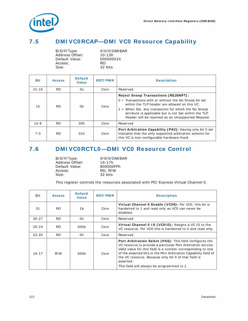
Direct Memory Interface Registers (DMIBAR)
222 Datasheet
7.5 DMIVC0RCAP—DMI VC0 Resource Capability
B/D/F/Type: 0/0/0/DMIBARAddress Offset: 10-13hDefault Value: 00000001hAccess: ROSize: 32 bits
7.6 DMIVC0RCTL0—DMI VC0 Resource Control
B/D/F/Type: 0/0/0/DMIBARAddress Offset: 14-17hDefault Value: 800000FFhAccess: RO, R/WSize: 32 bits
This register controls the resources associated with PCI Express Virtual Channel 0.
Bit AccessDefault Value
RST/PWR Description
31:16 RO 0s Core Reserved
15 RO 0b Core
Reject Snoop Transactions (REJSNPT):0 = Transactions with or without the No Snoop bit set
within the TLP header are allowed on this VC.1 = When Set, any transaction for which the No Snoop
attribute is applicable but is not Set within the TLP Header will be rejected as an Unsupported Request.
14:8 RO 00h Core Reserved
7:0 RO 01h CorePort Arbitration Capability (PAC): Having only bit 0 set indicates that the only supported arbitration scheme for this VC is non-configurable hardware-fixed.
Bit AccessDefault Value
RST/PWR Description
31 RO 1b CoreVirtual Channel 0 Enable (VC0E): For VC0, this bit is hardwired to 1 and read only as VC0 can never be disabled.
30:27 RO 0h Core Reserved
26:24 RO 000b CoreVirtual Channel 0 ID (VC0ID): Assigns a VC ID to the VC resource. For VC0 this is hardwired to 0 and read only.
23:20 RO 0h Core Reserved
19:17 R/W 000b Core
Port Arbitration Select (PAS): This field configures the VC resource to provide a particular Port Arbitration service. Valid value for this field is a number corresponding to one of the asserted bits in the Port Arbitration Capability field of the VC resource. Because only bit 0 of that field is asserted.This field will always be programmed to 1.

Datasheet 223
Direct Memory Interface Registers (DMIBAR)
7.7 DMIVC0RSTS—DMI VC0 Resource Status
B/D/F/Type: 0/0/0/DMIBARAddress Offset: 1A-1BhDefault Value: 0002hAccess: ROSize: 16 bits
This register reports the Virtual Channel specific status.
16:8 RO 000h Core Reserved
7:1 R/W 7Fh Core
Traffic Class / Virtual Channel 0 Map (TCVC0M): This field indicates the TCs (Traffic Classes) that are mapped to the VC resource. Bit locations within this field correspond to TC values.For example, when bit 7 is set in this field, TC7 is mapped to this VC resource. When more than one bit in this field is set, it indicates that multiple TCs are mapped to the VC resource. To remove one or more TCs from the TC/VC Map of an enabled VC, software must ensure that no new or outstanding transactions with the TC labels are targeted at the given Link.
0 RO 1b CoreTraffic Class 0 / Virtual Channel 0 Map (TC0VC0M): Traffic Class 0 is always routed to VC0.
Bit AccessDefault Value
RST/PWR Description
Bit AccessDefault Value
RST/PWR Description
15:2 RO 0000h CoreReserved: Reserved and Zero for future R/WC/S implementations. Software must use 0 for writes to these bits.
1 RO 1b Core
Virtual Channel 0 Negotiation Pending (VC0NP): 0 = The VC negotiation is complete.1 = The VC resource is still in the process of negotiation
(initialization or disabling).This bit indicates the status of the process of Flow Control initialization. It is set by default on Reset, as well as whenever the corresponding Virtual Channel is Disabled or the Link is in the DL_Down state.It is cleared when the link successfully exits the FC_INIT2 state.BIOS Requirement: Before using a Virtual Channel, software must check whether the VC Negotiation Pending fields for that Virtual Channel are cleared in both Components on a Link.
0 RO 0b Core Reserved

Direct Memory Interface Registers (DMIBAR)
224 Datasheet
7.8 DMIVC1RCAP—DMI VC1 Resource Capability
B/D/F/Type: 0/0/0/DMIBARAddress Offset: 1C-1FhDefault Value: 00008001hAccess: ROSize: 32 bits
7.9 DMIVC1RCTL1—DMI VC1 Resource Control
B/D/F/Type: 0/0/0/DMIBARAddress Offset: 20-23hDefault Value: 01000000hAccess: R/W, ROSize: 32 bits
This register controls the resources associated with PCI Express Virtual Channel 1.
Bit AccessDefault Value
RST/PWR Description
31:16 RO 0s Core Reserved
15 RO 1b Core
Reject Snoop Transactions (REJSNPT): 0 = Transactions with or without the No Snoop bit set
within the TLP header are allowed on this VC.1 = When Set, any transaction for which the No Snoop
attribute is applicable but is not Set within the TLP Header will be rejected as an Unsupported Request.
14:8 RO 00h Core Reserved
7:0 RO 01h CorePort Arbitration Capability (PAC): Having only bit 0 set indicates that the only supported arbitration scheme for this VC is non-configurable hardware-fixed.

Datasheet 225
Direct Memory Interface Registers (DMIBAR)
Bit AccessDefault Value
RST/PWR Description
31 R/W 0b Core
Virtual Channel 1 Enable (VC1E): 0 = Virtual Channel is disabled.1 = Virtual Channel is enabled. See exceptions below.Software must use the VC Negotiation Pending bit to check whether the VC negotiation is complete. When VC Negotiation Pending bit is cleared, a 1 read from this VC Enable bit indicates that the VC is enabled (Flow Control Initialization is completed for the PCI Express port). A 0 read from this bit indicates that the Virtual Channel is currently disabled.
BIOS Requirement:1. To enable a Virtual Channel, the VC Enable bits for
that Virtual Channel must be set in both Components on a Link.
2. To disable a Virtual Channel, the VC Enable bits for that Virtual Channel must be cleared in both Components on a Link.
3. Software must ensure that no traffic is using a Virtual Channel at the time it is disabled.
4. Software must fully disable a Virtual Channel in both Components on a Link before re-enabling the Virtual Channel.
30:27 RO 0h Core Reserved
26:24 R/W 001b CoreVirtual Channel 1 ID (VC1ID): Assigns a VC ID to the VC resource. Assigned value must be non-zero. This field can not be modified when the VC is already enabled.
23:20 RO 0h Core Reserved
19:17 R/W 000b Core
Port Arbitration Select (PAS): This field configures the VC resource to provide a particular Port Arbitration service. Valid value for this field is a number corresponding to one of the asserted bits in the Port Arbitration Capability field of the VC resource.
16:8 RO 000h Core Reserved
7:1 R/W 00h Core
Traffic Class / Virtual Channel 1 Map (TCVC1M): This field indicates the TCs (Traffic Classes) that are mapped to the VC resource. Bit locations within this field correspond to TC values.For example, when bit 7 is set in this field, TC7 is mapped to this VC resource. When more than one bit in this field is set, it indicates that multiple TCs are mapped to the VC resource. In order to remove one or more TCs from the TC/VC Map of an enabled VC, software must ensure that no new or outstanding transactions with the TC labels are targeted at the given Link.
0 RO 0b CoreTraffic Class 0 / Virtual Channel 1 Map (TC0VC1M): Traffic Class 0 is always routed to VC0.

Direct Memory Interface Registers (DMIBAR)
226 Datasheet
7.10 DMIVC1RSTS—DMI VC1 Resource Status
B/D/F/Type: 0/0/0/DMIBARAddress Offset: 26-27hDefault Value: 0002hAccess: ROSize: 16 bits
This register reports the Virtual Channel specific status.
Bit AccessDefault Value
RST/PWR Description
15:2 RO 0000h Core Reserved
1 RO 1b Core
Virtual Channel 1 Negotiation Pending (VC1NP): 0 = The VC negotiation is complete.1 = The VC resource is still in the process of negotiation
(initialization or disabling).Software may use this bit when enabling or disabling the VC. This bit indicates the status of the process of Flow Control initialization. It is set by default on Reset, as well as whenever the corresponding Virtual Channel is Disabled or the Link is in the DL_Down state. It is cleared when the link successfully exits the FC_INIT2 state.Before using a Virtual Channel, software must check whether the VC Negotiation Pending fields for that Virtual Channel are cleared in both Components on a Link.
0 RO 0b Core Reserved
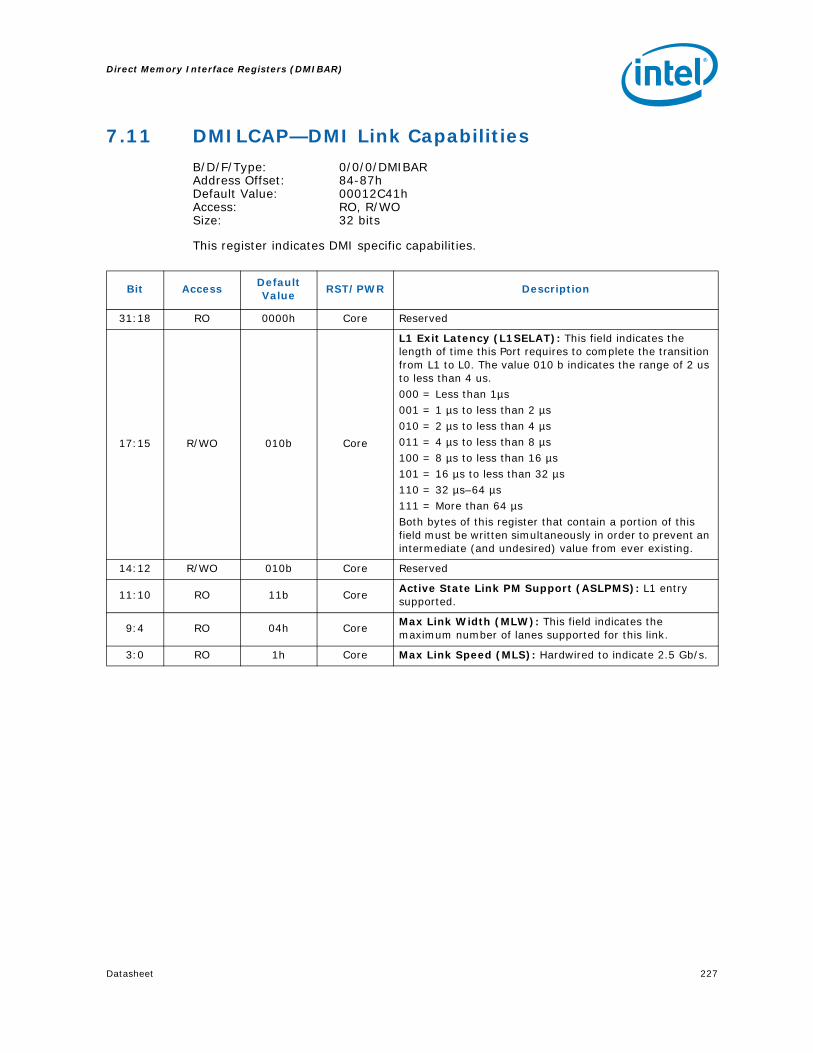
Datasheet 227
Direct Memory Interface Registers (DMIBAR)
7.11 DMILCAP—DMI Link Capabilities
B/D/F/Type: 0/0/0/DMIBARAddress Offset: 84-87hDefault Value: 00012C41hAccess: RO, R/WOSize: 32 bits
This register indicates DMI specific capabilities.
Bit AccessDefault Value
RST/PWR Description
31:18 RO 0000h Core Reserved
17:15 R/WO 010b Core
L1 Exit Latency (L1SELAT): This field indicates the length of time this Port requires to complete the transition from L1 to L0. The value 010 b indicates the range of 2 us to less than 4 us.000 = Less than 1µs001 = 1 µs to less than 2 µs010 = 2 µs to less than 4 µs011 = 4 µs to less than 8 µs100 = 8 µs to less than 16 µs101 = 16 µs to less than 32 µs110 = 32 µs–64 µs111 = More than 64 µsBoth bytes of this register that contain a portion of this field must be written simultaneously in order to prevent an intermediate (and undesired) value from ever existing.
14:12 R/WO 010b Core Reserved
11:10 RO 11b CoreActive State Link PM Support (ASLPMS): L1 entry supported.
9:4 RO 04h CoreMax Link Width (MLW): This field indicates the maximum number of lanes supported for this link.
3:0 RO 1h Core Max Link Speed (MLS): Hardwired to indicate 2.5 Gb/s.

Direct Memory Interface Registers (DMIBAR)
228 Datasheet
7.12 DMILCTL—DMI Link Control
B/D/F/Type: 0/0/0/DMIBARAddress Offset: 88-89hDefault Value: 0000hAccess: RO, R/WSize: 16 bits
This register allows control of DMI.
7.13 DMILSTS—DMI Link Status
B/D/F/Type: 0/0/0/DMIBARAddress Offset: 8A-8BhDefault Value: 0001hAccess: ROSize: 16 bits
This register indicates DMI status.
§ §
Bit AccessDefault Value
RST/PWR Description
15:2 RO 00h Core Reserved
7 R/W 0b Core Reserved
6:2 RO 0h Core Reserved
1:0 R/W 00b Core
Active State Power Management Support (ASPMS): This register controls the level of active state power management supported on the given link.00 = Disabled01 = Reserved10 = L1 Entry Enabled11 = L1 Entry Enabled
Bit AccessDefault Value
RST/PWR Description
15:10 RO 00h Core Reserved
9:4 RO 00h Core
Negotiated Width (NWID): This register indicates negotiated link width. This field is valid only when the link is in the L0 or L1 states (after link width negotiation is successfully completed).00h = Reserved01h = X102h = X204h = X4All other encodings are reserved.
3:0 RO 1h Core
Negotiated Speed (NSPD): This field indicates negotiated link speed.1h = 2.5 Gb/sAll other encodings are reserved.

Datasheet 229
Host-Secondary PCI Express* Bridge Registers (D6:F0) (Intel® 82P45 MCH Only)
8 Host-Secondary PCI Express* Bridge Registers (D6:F0) (Intel® 82P45 MCH Only)
Device 6 contains the controls associated with the PCI Express root port that is the intended attach point for external devices. In addition, it also functions as the virtual PCI-to-PCI bridge. Table 14 provides an address map of the D1:F0 registers listed by address offset in ascending order. This chapter provides a detailed bit description of the registers.
Warning: When reading the PCI Express "conceptual" registers such as this, you may not get a valid value unless the register value is stable.
The PCI Express* Specification defines two types of reserved bits:
Reserved and Preserved:
• Reserved for future RW implementations; software must preserve value read for writes to bits.
• Reserved and Zero: Reserved for future R/WC/S implementations; software must use 0 for writes to bits.
Unless explicitly documented as Reserved and Zero, all bits marked as reserved are part of the Reserved and Preserved type, which have historically been the typical definition for Reserved.
Note: Most (if not all) control bits in this device cannot be modified unless the link is down. Software is required to first disable the link, then program the registers, and then re-enable the link (which will cause a full-retrain with the new settings).
Table 14. Host-Secondary PCI Express* Bridge Register Address Map (D6:F0) (Sheet 1 of 3)
Address Offset
Register Symbol
Register NameDefault Value
Access
0–1h VID1 Vendor Identification 8086h RO
2–3h DID1 Device Identification 29E9h RO
4–5h PCICMD1 PCI Command 0000h RO, RW
6–7h PCISTS1 PCI Status 0010h RO, RWC
8h RID1 Revision IdentificationSee register description
RO
9–Bh CC1 Class Code 060400h RO
Ch CL1 Cache Line Size 00h RW
Eh HDR1 Header Type 01h RO
18h PBUSN1 Primary Bus Number 00h RO
19h SBUSN1 Secondary Bus Number 00h RW
1Ah SUBUSN1 Subordinate Bus Number 00h RW
1Ch IOBASE1 I/O Base Address F0h RO, RW

Host-Secondary PCI Express* Bridge Registers (D6:F0) (Intel® 82P45 MCH Only)
230 Datasheet
1Dh IOLIMIT1 I/O Limit Address 00h RW, RO
1E–1Fh SSTS1 Secondary Status 0000h RO, RWC
20–21h MBASE1 Memory Base Address FFF0h RW, RO
22–23h MLIMIT1 Memory Limit Address 0000h RW, RO
24–25h PMBASE1 Prefetchable Memory Base Address FFF1h RW, RO
26–27h PMLIMIT1 Prefetchable Memory Limit Address 0001h RO, RW
28–2Bh PMBASEU1 Prefetchable Memory Base Address Upper 00000000h RW
2C–2Fh PMLIMITU1 Prefetchable Memory Limit Address Upper 00000000h RW
34h CAPPTR1 Capabilities Pointer 88h RO
3Ch INTRLINE1 Interrupt Line 00h RW
3Dh INTRPIN1 Interrupt Pin 01h RO
3E–3Fh BCTRL1 Bridge Control 0000h RO, RW
80–83h PM_CAPID1 Power Management Capabilities C8039001h RO
84–87h PM_CS1 Power Management Control/Status 00000008hRO, RW, RW/P
88–8Bh SS_CAPID Subsystem ID and Vendor ID Capabilities 0000800Dh RO
8C–8Fh SS Subsystem ID and Subsystem Vendor ID 00008086h RWO
90–91h MSI_CAPID Message Signaled Interrupts Capability ID A005h RO
92–93h MC Message Control 0000h RW, RO
94–97h MA Message Address 00000000h RO, RW
98–99h MD Message Data 0000h RW
A0–A1h PE_CAPL PCI Express Capability List 0010h RO
A2–A3h PE_CAP PCI Express Capabilities 0142h RO, RWO
A4–A7h DCAP Device Capabilities 00008000h RO
A8–A9h DCTL Device Control 0000h RW, RO
AA–ABh DSTS Device Status 0000h RO, RWC
AC–AFh LCAP Link Capabilities 03214D02h RO, RWO
B0–B1h LCTL Link Control 0000hRO, RW, RW/SC
B2–hB3 LSTS Link Status 1000h RWC, RO
B4–B7h SLOTCAP Slot Capabilities 00040000h RWO, RO
B8–B9h SLOTCTL Slot Control 0000h RO, RW
BA–BBh SLOTSTS Slot Status 0000h RO, RWC
BC–BDh RCTL Root Control 0000h RO, RW
C0–C3h RSTS Root Status 00000000h RO, RWC
EC–EFh PELC PCI Express Legacy Control 00000000h RO, RW
Table 14. Host-Secondary PCI Express* Bridge Register Address Map (D6:F0) (Sheet 2 of 3)
Address Offset
Register Symbol
Register NameDefault Value
Access

Datasheet 231
Host-Secondary PCI Express* Bridge Registers (D6:F0) (Intel® 82P45 MCH Only)
8.1 VID1—Vendor Identification
B/D/F/Type: 0/6/0/PCIAddress Offset: 0–1hDefault Value: 8086hAccess: RO Size: 16 bits
This register combined with the Device Identification register uniquely identify any PCI device.
100–103h VCECHVirtual Channel Enhanced Capability Header
14010002h RO
104–107h PVCCAP1 Port VC Capability Register 1 00000000h RO
108–10Bh PVCCAP2 Port VC Capability Register 2 00000000h RO
10C–10Dh PVCCTL Port VC Control 0000h RO, RW
110–113h VC0RCAP VC0 Resource Capability 00000000h RO
114–117h VC0RCTL VC0 Resource Control 800000FFh RO, RW
11A–11Bh VC0RSTS VC0 Resource Status 0002h RO
140–143h RCLDECH Root Complex Link Declaration Enhanced 00010005h RO
144–147h ESD Element Self Description 03000100h RO, RWO
150–153h LE1D Link Entry 1 Description 00000000h RO, RWO
158–15Fh LE1A Link Entry 1 Address0000000000
000000hRO, RWO
Table 14. Host-Secondary PCI Express* Bridge Register Address Map (D6:F0) (Sheet 3 of 3)
Address Offset
Register Symbol
Register NameDefault Value
Access
Bit AccessDefault Value
RST/PWR
Description
15:0 RO 8086h Core Vendor Identification (VID1): PCI standard identification for Intel.

Host-Secondary PCI Express* Bridge Registers (D6:F0) (Intel® 82P45 MCH Only)
232 Datasheet
8.2 DID1—Device Identification
B/D/F/Type: 0/6/0/PCIAddress Offset: 2–3hDefault Value: 29E9hAccess: RO Size: 16 bits
This register combined with the Vendor Identification register uniquely identifies any PCI device.
8.3 PCICMD1—PCI Command
B/D/F/Type: 0/6/0/PCIAddress Offset: 4–5hDefault Value: 0000hAccess: RO, RW Size: 16 bits
Bit AccessDefault Value
RST/PWR
Description
15:8 RO 29h CoreDevice Identification Number (DID1(UB)): Identifier assigned to the MCH device #6 (virtual PCI-to-PCI bridge, PCI Express port).
7:4 RO Eh CoreDevice Identification Number (DID1(HW)): Identifier assigned to the MCH device #6 (virtual PCI-to-PCI bridge, PCI Express port).
3:0 RO 9h CoreDevice Identification Number (DID1(LB)): Identifier assigned to the MCH device #6 (virtual PCI-to-PCI bridge, PCI Express port).
Bit AccessDefault Value
RST/PWR
Description
15:11 RO 00h Core Reserved
10 RW 0b Core
INTA Assertion Disable (INTAAD): 0 = This device is permitted to generate INTA interrupt messages.1 = This device is prevented from generating interrupt messages. Any
INTA emulation interrupts already asserted must be de-asserted when this bit is set.
This bit only affects interrupts generated by the device (PCI INTA from a PME event) controlled by this command register. It does not affect upstream MSIs, upstream PCI INTA-INTD assert and de-assert messages.
9 RO 0b CoreFast Back-to-Back Enable (FB2B): Not Applicable or Implemented. Hardwired to 0.

Datasheet 233
Host-Secondary PCI Express* Bridge Registers (D6:F0) (Intel® 82P45 MCH Only)
8 RW 0b Core
SERR# Message Enable (SERRE1): This bit controls Device 6 SERR# messaging. The MCH communicates the SERR# condition by sending a SERR message to the ICH. This bit, when set, enables reporting of non-fatal and fatal errors detected by the device to the Root Complex. Note that errors are reported if enabled either through this bit or through the PCI-Express specific bits in the Device Control Register.0 = The SERR message is generated by the MCH for Device 6 only
under conditions enabled individually through the Device Control Register.
1 = The MCH is enabled to generate SERR messages which will be sent to the ICH for specific Device 6 error conditions generated/detected on the primary side of the virtual PCI to PCI bridge (not those received by the secondary side). The status of SERRs generated is reported in the PCISTS1 register.
7 RO 0b Core Reserved
6 RW 0b Core
Parity Error Response Enable (PERRE): Controls whether or not the Master Data Parity Error bit in the PCI Status register can bet set.0 = Master Data Parity Error bit in PCI Status register can NOT be set.1 = Master Data Parity Error bit in PCI Status register CAN be set.
5:3 RO 0b Core Reserved
2 RW 0b Core
Bus Master Enable (BME): Controls the ability of the PCI Express port to forward Memory and I/O Read/Write Requests in the upstream direction.0 = This device is prevented from making memory or IO requests to
its primary bus. Note that according to PCI Specification, as MSI interrupt messages are in-band memory writes, disabling the bus master enable bit prevents this device from generating MSI interrupt messages or passing them from its secondary bus to its primary bus. Upstream memory writes/reads, IO writes/reads, peer writes/reads, and MSIs will all be treated as illegal cycles. Writes are forwarded to memory address C0000h with byte enables de-asserted. Reads will be forwarded to memory address C0000h and will return Unsupported Request status (or Master abort) in its completion packet.
1 = This device is allowed to issue requests to its primary bus. Completions for previously issued memory read requests on the primary bus will be issued when the data is available.
This bit does not affect forwarding of Completions from the primary interface to the secondary interface.
1 RW 0b Core
Memory Access Enable (MAE): 0 = All of device #6's memory space is disabled.1 = Enable the Memory and Pre-fetchable memory address ranges
defined in the MBASE1, MLIMIT1, PMBASE1, and PMLIMIT1 registers.
0 RW 0b Core
IO Access Enable (IOAE): 0 = All of device #6's I/O space is disabled.1 = Enable the I/O address range defined in the IOBASE1, and
IOLIMIT1 registers.
Bit AccessDefault Value
RST/PWR
Description

Host-Secondary PCI Express* Bridge Registers (D6:F0) (Intel® 82P45 MCH Only)
234 Datasheet
8.4 PCISTS1—PCI Status
B/D/F/Type: 0/6/0/PCIAddress Offset: 6–7hDefault Value: 0010hAccess: RO, RWC Size: 16 bits
This register reports the occurrence of error conditions associated with primary side of the "virtual" Host-PCI Express bridge embedded within the MCH.
Bit AccessDefault Value
RST/PWR
Description
15 RO 0b CoreDetected Parity Error (DPE): Not Applicable or Implemented. Hardwired to 0. Parity (generating poisoned Transaction Layer Packets) is not supported on the primary side of this device.
14 RWC 0b Core
Signaled System Error (SSE): This bit is set when this Device sends a SERR due to detecting an ERR_FATAL or ERR_NONFATAL condition and the SERR Enable bit in the Command register is 1. Both received (if enabled by BCTRL1[1]) and internally detected error messages do not affect this field).
13 RO 0b CoreReceived Master Abort Status (RMAS): Not Applicable or Implemented. Hardwired to 0. The concept of a master abort does not exist on primary side of this device.
12 RO 0b CoreReceived Target Abort Status (RTAS): Not Applicable or Implemented. Hardwired to 0. The concept of a target abort does not exist on primary side of this device.
11 RO 0b CoreSignaled Target Abort Status (STAS): Not Applicable or Implemented. Hardwired to 0. The concept of a target abort does not exist on primary side of this device.
10:9 RO 00b CoreDEVSELB Timing (DEVT): This device is not the subtractively decoded device on bus 0. This bit field is therefore hardwired to 00 to indicate that the device uses the fastest possible decode.
8 RO 0b Core
Master Data Parity Error (PMDPE): Because the primary side of the PCI Express's virtual peer-to-peer bridge is integrated with the MCH functionality, there is no scenario where this bit will get set. Because hardware will never set this bit, it is impossible for software to have an opportunity to clear this bit or otherwise test that it is implemented. The PCI specification defines it as a R/WC, but for our implementation an RO definition behaves the same way and will meet all Microsoft testing requirements. This bit can only be set when the Parity Error Enable bit in the PCI Command register is set.
7 RO 0b CoreFast Back-to-Back (FB2B): Not Applicable or Implemented. Hardwired to 0.
6 RO 0b Core Reserved
5 RO 0b Core66/60MHz capability (CAP66): Not Applicable or Implemented. Hardwired to 0.
4 RO 1b CoreCapabilities List (CAPL): Indicates that a capabilities list is present. Hardwired to 1.

Datasheet 235
Host-Secondary PCI Express* Bridge Registers (D6:F0) (Intel® 82P45 MCH Only)
8.5 RID1—Revision Identification
B/D/F/Type: 0/6/0/PCIAddress Offset: 8hDefault Value: see description belowAccess: RO Size: 8 bits
This register contains the revision number of the MCH device 6. These bits are read only and writes to this register have no effect.
8.6 CC1—Class Code
B/D/F/Type: 0/6/0/PCIAddress Offset: 9–BhDefault Value: 060400hAccess: RO Size: 24 bits
This register identifies the basic function of the device, a more specific sub-class, and a register-specific programming interface.
3 RO 0b Core
INTA Status (INTAS): Indicates that an interrupt message is pending internally to the device. Only PME sources feed into this status bit (not PCI INTA-INTD assert and de-assert messages). The INTA Assertion Disable bit, PCICMD1[10], has no effect on this bit.
2:0 RO 000b Core Reserved
Bit AccessDefault Value
RST/PWR
Description
Bit AccessDefault Value
RST/PWR
Description
7:0 ROsee
descriptionCore
Revision Identification Number (RID1): This is an 8-bit value that indicates the revision identification number for the MCH Device 0. Refer to the Intel® 4 Series Chipset Specification Update for the value of this register.
Bit AccessDefault Value
RST/PWR
Description
23:16 RO 06h CoreBase Class Code (BCC): Indicates the base class code for this device. This code has the value 06h, indicating a Bridge device.
15:8 RO 04h CoreSub-Class Code (SUBCC): Indicates the sub-class code for this device. The code is 04h indicating a PCI to PCI Bridge.
7:0 RO 00h CoreProgramming Interface (PI): Indicates the programming interface of this device. This value does not specify a particular register set layout and provides no practical use for this device.

Host-Secondary PCI Express* Bridge Registers (D6:F0) (Intel® 82P45 MCH Only)
236 Datasheet
8.7 CL1—Cache Line Size
B/D/F/Type: 0/6/0/PCIAddress Offset: ChDefault Value: 00hAccess: RW Size: 8 bits
8.8 HDR1—Header Type
B/D/F/Type: 0/6/0/PCIAddress Offset: EhDefault Value: 01hAccess: RO Size: 8 bits
This register identifies the header layout of the configuration space. No physical register exists at this location.
8.9 PBUSN1—Primary Bus Number
B/D/F/Type: 0/6/0/PCIAddress Offset: 18hDefault Value: 00hAccess: RO Size: 8 bits
This register identifies that this "virtual" Host-PCI Express bridge is connected to PCI bus #0.
Bit AccessDefault Value
RST/PWR
Description
7:0 RW 00h CoreCache Line Size (Scratch pad): Implemented by PCI Express devices as a read-write field for legacy compatibility purposes but has no impact on any PCI Express device functionality.
Bit AccessDefault Value
Description
7:0 RO 01h CoreHeader Type Register (HDR): Returns 01h to indicate that this is a single function device with bridge header layout.
Bit AccessDefault Value
RST/PWR
Description
7:0 RO 00h Core
Primary Bus Number (BUSN): Configuration software typically programs this field with the number of the bus on the primary side of the bridge. Since device #6 is an internal device and its primary bus is always 0, these bits are read only and are hardwired to 0.

Datasheet 237
Host-Secondary PCI Express* Bridge Registers (D6:F0) (Intel® 82P45 MCH Only)
8.10 SBUSN1—Secondary Bus Number
B/D/F/Type: 0/6/0/PCIAddress Offset: 19hDefault Value: 00hAccess: RW Size: 8 bits
This register identifies the bus number assigned to the second bus side of the "virtual" bridge. This number is programmed by the PCI configuration software to allow mapping of configuration cycles to PCI Express.
8.11 SUBUSN1—Subordinate Bus Number
B/D/F/Type: 0/6/0/PCIAddress Offset: 1AhDefault Value: 00hAccess: RW Size: 8 bits
This register identifies the subordinate bus (if any) that resides at the level below PCI Express. This number is programmed by the PCI configuration software to allow mapping of configuration cycles to PCI Express.
Bit AccessDefault Value
RST/PWR
Description
7:0 RW 00h CoreSecondary Bus Number (BUSN): This field is programmed by configuration software with the bus number assigned to PCI Express.
Bit AccessDefault Value
RST/PWR
Description
7:0 RW 00h Core
Subordinate Bus Number (BUSN): This register is programmed by configuration software with the number of the highest subordinate bus that lies behind the device #6 bridge. When only a single PCI device resides on the PCI Express segment, this register will contain the same value as the SBUSN1 register.

Host-Secondary PCI Express* Bridge Registers (D6:F0) (Intel® 82P45 MCH Only)
238 Datasheet
8.12 IOBASE1—I/O Base Address
B/D/F/Type: 0/6/0/PCIAddress Offset: 1ChDefault Value: F0hAccess: RO, RW Size: 8 bits
This register controls the processor to PCI Express I/O access routing based on the following formula:
IO_BASE ≤ address ≤ IO_LIMIT
Only upper 4 bits are programmable. For the purpose of address decode address bits A[11:0] are treated as 0. Thus the bottom of the defined I/O address range will be aligned to a 4 KB boundary.
8.13 IOLIMIT1—I/O Limit Address
B/D/F/Type: 0/6/0/PCIAddress Offset: 1DhDefault Value: 00hAccess: RW, RO Size: 8 bits
This register controls the processor to PCI Express I/O access routing based on the following formula:
IO_BASE ≤ address ≤ IO_LIMIT
Only upper 4 bits are programmable. For the purpose of address decode address bits A[11:0] are assumed to be FFFh. Thus, the top of the defined I/O address range will be at the top of a 4 KB aligned address block.
Bit AccessDefault Value
RST/PWR
Description
7:4 RW Fh CoreI/O Address Base (IOBASE): This field corresponds to A[15:12] of the I/O addresses passed by bridge 1 to PCI Express.
3:0 RO 0h Core Reserved
Bit AccessDefault Value
RST/PWR
Description
7:4 RW 0h Core
I/O Address Limit (IOLIMIT): Corresponds to A[15:12] of the I/O address limit of device #6. Devices between this upper limit and IOBASE1 will be passed to the PCI Express hierarchy associated with this device.
3:0 RO 0h Core Reserved

Datasheet 239
Host-Secondary PCI Express* Bridge Registers (D6:F0) (Intel® 82P45 MCH Only)
8.14 SSTS1—Secondary Status
B/D/F/Type: 0/6/0/PCIAddress Offset: 1E–1FhDefault Value: 0000hAccess: RO, RWC Size: 16 bits
SSTS1 is a 16-bit status register that reports the occurrence of error conditions associated with secondary side of the "virtual" PCI-PCI bridge embedded within MCH.
Bit AccessDefault Value
RST/PWR
Description
15 RWC 0b Core
Detected Parity Error (DPE): This bit is set by the Secondary Side for a Type 1 Configuration Space header device whenever it receives a Poisoned Transaction Layer Packet, regardless of the state of the Parity Error Response Enable bit in the Bridge Control Register.
14 RWC 0b CoreReceived System Error (RSE): This bit is set when the Secondary Side for a Type 1 configuration space header device receives an ERR_FATAL or ERR_NONFATAL.
13 RWC 0b Core
Received Master Abort (RMA): This bit is set when the Secondary Side for Type 1 Configuration Space Header Device (for requests initiated by the Type 1 Header Device itself) receives a Completion with Unsupported Request Completion Status.
12 RWC 0b Core
Received Target Abort (RTA): This bit is set when the Secondary Side for Type 1 Configuration Space Header Device (for requests initiated by the Type 1 Header Device itself) receives a Completion with Completer Abort Completion Status.
11 RO 0b Core
Signaled Target Abort (STA): Not Applicable or Implemented. Hardwired to 0. The MCH does not generate Target Aborts (the MCH will never complete a request using the Completer Abort Completion status).
10:9 RO 00b CoreDEVSELB Timing (DEVT): Not Applicable or Implemented. Hardwired to 0.
8 RWC 0b Core
Master Data Parity Error (SMDPE): When set, indicates that the MCH received across the link (upstream) a Read Data Completion Poisoned Transaction Layer Packet (EP=1). This bit can only be set when the Parity Error Enable bit in the Bridge Control register is set.
7 RO 0b CoreFast Back-to-Back (FB2B): Not Applicable or Implemented. Hardwired to 0.
6 RO 0b Core Reserved
5 RO 0b Core66/60 MHz capability (CAP66): Not Applicable or Implemented. Hardwired to 0.
4:0 RO 00h Core Reserved

Host-Secondary PCI Express* Bridge Registers (D6:F0) (Intel® 82P45 MCH Only)
240 Datasheet
8.15 MBASE1—Memory Base Address
B/D/F/Type: 0/6/0/PCIAddress Offset: 20–21hDefault Value: FFF0hAccess: RW, RO Size: 16 bits
This register controls the processor to PCI Express non-prefetchable memory access routing based on the following formula:
MEMORY_BASE ≤ address ≤ MEMORY_LIMIT
The upper 12 bits of the register are read/write and correspond to the upper 12 address bits A[31:20] of the 32 bit address. The bottom 4 bits of this register are read-only and return zeroes when read. This register must be initialized by the configuration software. For the purpose of address decode address bits A[19:0] are assumed to be 0. Thus, the bottom of the defined memory address range will be aligned to a 1 MB boundary.
Bit AccessDefault Value
RST/PWR
Description
15:4 RW FFFh CoreMemory Address Base (MBASE): Corresponds to A[31:20] of the lower limit of the memory range that will be passed to PCI Express.
3:0 RO 0h Core Reserved

Datasheet 241
Host-Secondary PCI Express* Bridge Registers (D6:F0) (Intel® 82P45 MCH Only)
8.16 MLIMIT1—Memory Limit Address
B/D/F/Type: 0/6/0/PCIAddress Offset: 22–23hDefault Value: 0000hAccess: RW, RO Size: 16 bits
This register controls the processor to PCI Express non-prefetchable memory access routing based on the following formula:
MEMORY_BASE ≤ address ≤ MEMORY_LIMIT
The upper 12 bits of the register are read/write and correspond to the upper 12 address bits A[31:20] of the 32 bit address. The bottom 4 bits of this register are read-only and return zeroes when read. This register must be initialized by the configuration software. For the purpose of address decode, address bits A[19:0] are assumed to be FFFFFh. Thus, the top of the defined memory address range will be at the top of a 1 MB aligned memory block.
Note: Memory range covered by MBASE and MLIMIT registers are used to map non-prefetchable PCI Express address ranges (typically where control/status memory-mapped I/O data structures of the controller will reside) and PMBASE and PMLIMIT are used to map prefetchable address ranges (typically device local memory). This segregation allows application of USWC space attribute to be performed in a true plug-and-play manner to the prefetchable address range for improved processor- PCI Express memory access performance.
Note: Configuration software is responsible for programming all address range registers (prefetchable, non-prefetchable) with the values that provide exclusive address ranges (i.e., prevent overlap with each other and/or with the ranges covered with the main memory). There is no provision in the MCH hardware to enforce prevention of overlap and operations of the system in the case of overlap are not ensured.
Bit AccessDefault Value
RST/PWR
Description
15:4 RW 000h CoreMemory Address Limit (MLIMIT): Corresponds to A[31:20] of the upper limit of the address range passed to PCI Express.
3:0 RO 0h Core Reserved

Host-Secondary PCI Express* Bridge Registers (D6:F0) (Intel® 82P45 MCH Only)
242 Datasheet
8.17 PMBASE1—Prefetchable Memory Base Address Upper
B/D/F/Type: 0/6/0/PCIAddress Offset: 24–25hDefault Value: FFF1hAccess: RW, RO Size: 16 bits
This register in conjunction with the corresponding Upper Base Address register controls the processor to PCI Express prefetchable memory access routing based on the following formula:
PREFETCHABLE_MEMORY_BASE ≤ address ≤ PREFETCHABLE_MEMORY_LIMIT
The upper 12 bits of this register are read/write and correspond to address bits A[31:20] of the 40-bit address. The lower 8 bits of the Upper Base Address register are read/write and correspond to address bits A[39:32] of the 40-bit address. This register must be initialized by the configuration software. For the purpose of address decode, address bits A[19:0] are assumed to be 0. Thus, the bottom of the defined memory address range will be aligned to a 1 MB boundary.
Bit AccessDefault Value
RST/PWR
Description
15:4 RW FFFh CorePrefetchable Memory Base Address (MBASE): Corresponds to A[31:20] of the lower limit of the memory range that will be passed to PCI Express.
3:0 RO 1h Core64-bit Address Support: Indicates that the upper 32 bits of the prefetchable memory region base address are contained in the Prefetchable Memory base Upper Address register at 28h.

Datasheet 243
Host-Secondary PCI Express* Bridge Registers (D6:F0) (Intel® 82P45 MCH Only)
8.18 PMLIMIT1—Prefetchable Memory Limit Address
B/D/F/Type: 0/6/0/PCIAddress Offset: 26–27hDefault Value: 0001hAccess: RO, RW Size: 16 bits
This register in conjunction with the corresponding Upper Limit Address register controls the processor to PCI Express prefetchable memory access routing based on the following formula:
PREFETCHABLE_MEMORY_BASE ≤ address ≤ PREFETCHABLE_MEMORY_LIMIT
The upper 12 bits of this register are read/write and correspond to address bits A[31:20] of the 40-bit address. The lower 8 bits of the Upper Limit Address register are read/write and correspond to address bits A[39:32] of the 40-bit address. This register must be initialized by the configuration software. For the purpose of address decode, address bits A[19:0] are assumed to be FFFFFh. Thus, the top of the defined memory address range will be at the top of a 1 MB aligned memory block. Note that prefetchable memory range is supported to allow segregation by the configuration software between the memory ranges that must be defined as UC and the ones that can be designated as a USWC (i.e., prefetchable) from the processor perspective.
Bit AccessDefault Value
RST/PWR
Description
15:4 RW 000h CorePrefetchable Memory Address Limit (PMLIMIT): This field corresponds to A[31:20] of the upper limit of the address range passed to PCI Express.
3:0 RO 1h Core64-bit Address Support: This field indicates that the upper 32 bits of the prefetchable memory region limit address are contained in the Prefetchable Memory Base Limit Address register at 2Ch

Host-Secondary PCI Express* Bridge Registers (D6:F0) (Intel® 82P45 MCH Only)
244 Datasheet
8.19 PMBASEU1—Prefetchable Memory Base Address Upper
B/D/F/Type: 0/6/0/PCIAddress Offset: 28–2BhDefault Value: 00000000hAccess: RW Size: 32 bits
The functionality associated with this register is present in the PCI Express design implementation.
This register in conjunction with the corresponding Upper Base Address register controls the processor to PCI Express prefetchable memory access routing based on the following formula:
PREFETCHABLE_MEMORY_BASE ≤ address ≤ PREFETCHABLE_MEMORY_LIMIT
The upper 12 bits of this register are read/write and correspond to address bits A[31:20] of the 40-bit address. The lower 8 bits of the Upper Base Address register are read/write and correspond to address bits A[39:32] of the 40-bit address. This register must be initialized by the configuration software. For the purpose of address decode, address bits A[19:0] are assumed to be 0. Thus, the bottom of the defined memory address range will be aligned to a 1 MB boundary.
Bit AccessDefault Value
RST/PWR
Description
31:0 RW0000000
0hCore
Prefetchable Memory Base Address (MBASEU): This field corresponds to A[63:32] of the lower limit of the prefetchable memory range that will be passed to PCI Express.

Datasheet 245
Host-Secondary PCI Express* Bridge Registers (D6:F0) (Intel® 82P45 MCH Only)
8.20 PMLIMITU1—Prefetchable Memory Limit Address Upper
B/D/F/Type: 0/6/0/PCIAddress Offset: 2C–2FhDefault Value: 00000000hAccess: RW Size: 32 bits
The functionality associated with this register is present in the PCI Express design implementation.
This register in conjunction with the corresponding Upper Limit Address register controls the processor to PCI Express prefetchable memory access routing based on the following formula:
PREFETCHABLE_MEMORY_BASE ≤ address ≤ PREFETCHABLE_MEMORY_LIMIT
The upper 12 bits of this register are read/write and correspond to address bits A[31:20] of the 40- bit address. The lower 8 bits of the Upper Limit Address register are read/write and correspond to address bits A[39:32] of the 40-bit address. This register must be initialized by the configuration software. For the purpose of address decode, address bits A[19:0] are assumed to be FFFFFh. Thus, the top of the defined memory address range will be at the top of a 1MB aligned memory block.
Note that prefetchable memory range is supported to allow segregation by the configuration software between the memory ranges that must be defined as UC and the ones that can be designated as a USWC (i.e., prefetchable) from the processor perspective.
Bit AccessDefault Value
RST/PWR
Description
31:0 RW0000000
0hCore
Prefetchable Memory Address Limit (MLIMITU): This field corresponds to A[63:32] of the upper limit of the prefetchable Memory range that will be passed to PCI Express.

Host-Secondary PCI Express* Bridge Registers (D6:F0) (Intel® 82P45 MCH Only)
246 Datasheet
8.21 CAPPTR1—Capabilities Pointer
B/D/F/Type: 0/6/0/PCIAddress Offset: 34hDefault Value: 88hAccess: RO Size: 8 bits
The capabilities pointer provides the address offset to the location of the first entry in this device's linked list of capabilities.
8.22 INTRLINE1—Interrupt Line
B/D/F/Type: 0/6/0/PCIAddress Offset: 3ChDefault Value: 00hAccess: RW Size: 8 bits
This register contains interrupt line routing information. The device itself does not use this value, rather it is used by device drivers and operating systems to determine priority and vector information.
8.23 INTRPIN1—Interrupt Pin
B/D/F/Type: 0/6/0/PCIAddress Offset: 3DhDefault Value: 01hAccess: RO Size: 8 bits
This register specifies which interrupt pin this device uses.
Bit AccessDefault Value
RST/PWR
Description
7:0 RO 88h CoreFirst Capability (CAPPTR1): The first capability in the list is the Subsystem ID and Subsystem Vendor ID Capability.
Bit AccessDefault Value
RST/PWR
Description
7:0 RW 00h CoreInterrupt Connection (INTCON): Used to communicate interrupt line routing information.
Bit AccessDefault Value
RST/PWR
Description
7:0 RO 01h CoreInterrupt Pin (INTPIN): As a single function device, the PCI Express device specifies INTA as its interrupt pin. 01h=INTA.

Datasheet 247
Host-Secondary PCI Express* Bridge Registers (D6:F0) (Intel® 82P45 MCH Only)
8.24 BCTRL1—Bridge Control
B/D/F/Type: 0/6/0/PCIAddress Offset: 3E–3FhDefault Value: 0000hAccess: RO, RW Size: 16 bits
This register provides extensions to the PCICMD1 register that are specific to PCI-PCI bridges. The BCTRL provides additional control for the secondary interface as well as some bits that affect the overall behavior of the "virtual" Host-PCI Express bridge embedded in the MCH.
Bit AccessDefault Value
RST/PWR
Description
15:12 RO 0h Core Reserved
11 RO 0b CoreDiscard Timer SERR# Enable (DTSERRE): Not Applicable or Implemented. Hardwired to 0.
10 RO 0b CoreDiscard Timer Status (DTSTS): Not Applicable or Implemented. Hardwired to 0.
9 RO 0b CoreSecondary Discard Timer (SDT): Not Applicable or Implemented. Hardwired to 0.
8 RO 0b CorePrimary Discard Timer (PDT): Not Applicable or Implemented. Hardwired to 0.
7 RO 0b CoreFast Back-to-Back Enable (FB2BEN): Not Applicable or Implemented. Hardwired to 0.
6 RW 0b CoreSecondary Bus Reset (SRESET): Setting this bit triggers a hot reset on the corresponding PCI Express Port. This will force the LTSSM to transition to the Hot Reset state (via Recovery) from L0 or L1 states.
5 RO 0b CoreMaster Abort Mode (MAMODE): Does not apply to PCI Express. Hardwired to 0.
4 RW 0b Core
VGA 16-bit Decode (VGA16D): Enables the PCI-to-PCI bridge to provide 16-bit decoding of VGA I/O address precluding the decoding of alias addresses every 1 KB. This bit only has meaning if bit 3 (VGA Enable) of this register is also set to 1, enabling VGA I/O decoding and forwarding by the bridge.0 = Execute 10-bit address decodes on VGA I/O accesses.1 = Execute 16-bit address decodes on VGA I/O accesses.
3 RW 0b CoreVGA Enable (VGAEN): Controls the routing of processor initiated transactions targeting VGA compatible I/O and memory address ranges. See the VGAEN/MDAP table in device 0, offset 97h[0].
2 RW 0b Core
ISA Enable (ISAEN): Needed to exclude legacy resource decode to route ISA resources to legacy decode path. Modifies the response by the MCH to an I/O access issued by the processor that target ISA I/O addresses. This applies only to I/O addresses that are enabled by the IOBASE and IOLIMIT registers. 0 = All addresses defined by the IOBASE and IOLIMIT for processor I/O
transactions will be mapped to PCI Express. 1 = MCH will not forward to PCI Express any I/O transactions addressing
the last 768 bytes in each 1 KB block even if the addresses are within the range defined by the IOBASE and IOLIMIT registers.

Host-Secondary PCI Express* Bridge Registers (D6:F0) (Intel® 82P45 MCH Only)
248 Datasheet
8.25 PM_CAPID1—Power Management Capabilities
B/D/F/Type: 0/6/0/PCIAddress Offset: 80–83hDefault Value: C8039001hAccess: RO Size: 32 bits
1 RW 0b Core
SERR Enable (SERREN): 0 = No forwarding of error messages from secondary side to primary side
that could result in an SERR.1 = ERR_COR, ERR_NONFATAL, and ERR_FATAL messages result in SERR
message when individually enabled by the Root Control register.
0 RW 0b Core
Parity Error Response Enable (PEREN): Controls whether or not the Master Data Parity Error bit in the Secondary Status register is set when the MCH receives across the link (upstream) a Read Data Completion Poisoned Transaction Layer Packet.0 = Master Data Parity Error bit in Secondary Status register can NOT be
set.1 = Master Data Parity Error bit in Secondary Status register CAN be set.
Bit AccessDefault Value
RST/PWR
Description
Bit AccessDefault Value
RST/PWR
Description
31:27 RO 19h Core
PME Support (PMES): This field indicates the power states in which this device may indicate PME wake via PCI Express messaging. D0, D3hot & D3cold. This device is not required to do anything to support D3hot and D3cold, it simply must report that those states are supported. Refer to the PCI Power Management 1.1 specification for encoding explanation and other power management details.
26 RO 0b CoreD2 Power State Support (D2PSS): Hardwired to 0 to indicate that the D2 power management state is NOT supported.
25 RO 0b CoreD1 Power State Support (D1PSS): Hardwired to 0 to indicate that the D1 power management state is NOT supported.
24:22 RO 000b CoreAuxiliary Current (AUXC): Hardwired to 0 to indicate that there are no 3.3Vaux auxiliary current requirements.
21 RO 0b CoreDevice Specific Initialization (DSI): Hardwired to 0 to indicate that special initialization of this device is NOT required before generic class device driver is to use it.
20 RO 0b Core Auxiliary Power Source (APS): Hardwired to 0.
19 RO 0b CorePME Clock (PMECLK): Hardwired to 0 to indicate this device does NOT support PMEB generation.
18:16 RO 011b CorePCI PM CAP Version (PCIPMCV): A value of 011b indicates that this function complies with PCI Power Management Interface Specification, Revision 1.2.
15:8 RO 90h Core
Pointer to Next Capability (PNC): This contains a pointer to the next item in the capabilities list. If MSICH (CAPL[0] @ 7Fh) is 0, then the next item in the capabilities list is the Message Signaled Interrupts (MSI) capability at 90h.
7:0 RO 01h CoreCapability ID (CID): Value of 01h identifies this linked list item (capability structure) as being for PCI Power Management registers.

Datasheet 249
Host-Secondary PCI Express* Bridge Registers (D6:F0) (Intel® 82P45 MCH Only)
8.26 PM_CS1—Power Management Control/Status
B/D/F/Type: 0/6/0/PCIAddress Offset: 84–87hDefault Value: 00000008hAccess: RO, RW, RW/P Size: 32 bits
Bit AccessDefault Value
RST/PWR
Description
31:16 RO 0000h Core Reserved
15 RO 0b CorePME Status (PMESTS): This bit indicates that this device does not support PMEB generation from D3cold.
14:13 RO 00b CoreData Scale (DSCALE): This field indicates that this device does not support the power management data register.
12:9 RO 0h CoreData Select (DSEL): This field indicates that this device does not support the power management data register.
8 RW/P 0b Core
PME Enable (PMEE): This bit indicates that this device does not generate PMEB assertion from any D-state.0 = PMEB generation not possible from any D State1 = PMEB generation enabled from any D StateThe setting of this bit has no effect on hardware.See PM_CAP[15:11]
7:2 RO 0000b Core Reserved
1:0 RW 00b Core
Power State (PS): This field indicates the current power state of this device and can be used to set the device into a new power state. If software attempts to write an unsupported state to this field, write operation must complete normally on the bus, but the data is discarded and no state change occurs.00 = D001 = D1 (Not supported in this device.)10 = D2 (Not supported in this device.)11 = D3Support of D3cold does not require any special action. While in the D3hot state, this device can only act as the target of PCI configuration transactions (for power management control). This device also cannot generate interrupts or respond to MMR cycles in the D3 state. The device must return to the D0 state in order to be fully-functional. When the Power State is other than D0, the bridge will Master Abort (i.e. not claim) any downstream cycles (with exception of type 0 config cycles). Consequently, these unclaimed cycles will go down DMI and come back up as Unsupported Requests, which the MCH logs as Master Aborts in Device 0 PCISTS[13]There is no additional hardware functionality required to support these Power States.

Host-Secondary PCI Express* Bridge Registers (D6:F0) (Intel® 82P45 MCH Only)
250 Datasheet
8.27 SS_CAPID—Subsystem ID and Vendor ID Capabilities
B/D/F/Type: 0/6/0/PCIAddress Offset: 88–8BhDefault Value: 0000800DhAccess: RO Size: 32 bits
This capability is used to uniquely identify the subsystem where the PCI device resides. Because this device is an integrated part of the system and not an add-in device, it is anticipated that this capability will never be used. However, it is necessary because Microsoft will test for its presence.
8.28 SS—Subsystem ID and Subsystem Vendor ID
B/D/F/Type: 0/6/0/PCIAddress Offset: 8C–8FhDefault Value: 00008086hAccess: RWO Size: 32 bits
System BIOS can be used as the mechanism for loading the SSID/SVID values. These values must be preserved through power management transitions and a hardware reset.
Bit AccessDefault Value
RST/PWR
Description
31:16 RO 0000h Core Reserved
15:8 RO 80h CorePointer to Next Capability (PNC): This field contains a pointer to the next item in the capabilities list which is the PCI Power Management capability.
7:0 RO 0Dh CoreCapability ID (CID): Value of 0Dh identifies this linked list item (capability structure) as being for SSID/SSVID registers in a PCI-to-PCI Bridge.
Bit AccessDefault Value
RST/PWR
Description
31:16 RWO 0000h CoreSubsystem ID (SSID): This bit identifies the particular subsystem and is assigned by the vendor.
15:0 RWO 8086h CoreSubsystem Vendor ID (SSVID): This field identifies the manufacturer of the subsystem and is the same as the vendor ID which is assigned by the PCI Special Interest Group.

Datasheet 251
Host-Secondary PCI Express* Bridge Registers (D6:F0) (Intel® 82P45 MCH Only)
8.29 MSI_CAPID—Message Signaled Interrupts Capability IDB/D/F/Type: 0/6/0/PCIAddress Offset: 90–91hDefault Value: A005hAccess: RO Size: 16 bits
When a device supports MSI, it can generate an interrupt request to the processor by writing a predefined data item (a message) to a predefined memory address.
8.30 MC—Message ControlB/D/F/Type: 0/6/0/PCIAddress Offset: 92–93hDefault Value: 0000hAccess: RW, RO Size: 16 bits
System software can modify bits in this register, but the device is prohibited from doing so.
If the device writes the same message multiple times, only one of those messages is guaranteed to be serviced. If all of them must be serviced, the device must not generate the same message again until the driver services the earlier one.
Bit AccessDefault Value
RST/PWR
Description
15:8 RO A0h CorePointer to Next Capability (PNC): This field contains a pointer to the next item in the capabilities list which is the PCI Express capability.
7:0 RO 05h CoreCapability ID (CID): Value of 05h identifies this linked list item (capability structure) as being for MSI registers.
Bit AccessDefault Value
RST/PWR
Description
15:8 RO 00h Core Reserved
7 RO 0b Core
64-bit Address Capable (64AC): Hardwired to 0 to indicate that the function does not implement the upper 32 bits of the Message Address register and is incapable of generating a 64-bit memory address.
6:4 RW 000b Core
Multiple Message Enable (MME): System software programs this field to indicate the actual number of messages allocated to this device. This number will be equal to or less than the number actually requested. The encoding is the same as for the MMC field below.
3:1 RO 000b Core
Multiple Message Capable (MMC): System software reads this field to determine the number of messages being requested by this device. The value of 000b equates to 1 message requested.000 = 1 message requestedAll other encodings are reserved.
0 RW 0b Core
MSI Enable (MSIEN): Controls the ability of this device to generate MSIs. 0 = MSI will not be generated. 1 = MSI will be generated when we receive PME messages. INTA will
not be generated and INTA Status (PCISTS1[3]) will not be set.
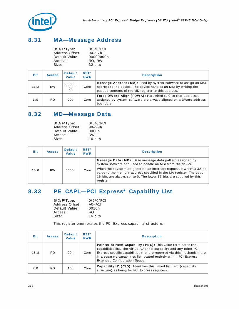
Host-Secondary PCI Express* Bridge Registers (D6:F0) (Intel® 82P45 MCH Only)
252 Datasheet
8.31 MA—Message Address
B/D/F/Type: 0/6/0/PCIAddress Offset: 94–97hDefault Value: 00000000hAccess: RO, RW Size: 32 bits
8.32 MD—Message Data
B/D/F/Type: 0/6/0/PCIAddress Offset: 98–99hDefault Value: 0000hAccess: RW Size: 16 bits
8.33 PE_CAPL—PCI Express* Capability List
B/D/F/Type: 0/6/0/PCIAddress Offset: A0–A1hDefault Value: 0010hAccess: RO Size: 16 bits
This register enumerates the PCI Express capability structure.
Bit AccessDefault Value
RST/PWR
Description
31:2 RW0000000
0hCore
Message Address (MA): Used by system software to assign an MSI address to the device. The device handles an MSI by writing the padded contents of the MD register to this address.
1:0 RO 00b CoreForce DWord Align (FDWA): Hardwired to 0 so that addresses assigned by system software are always aligned on a DWord address boundary.
Bit AccessDefault Value
RST/PWR
Description
15:0 RW 0000h Core
Message Data (MD): Base message data pattern assigned by system software and used to handle an MSI from the device. When the device must generate an interrupt request, it writes a 32-bit value to the memory address specified in the MA register. The upper 16-bits are always set to 0. The lower 16-bits are supplied by this register.
Bit AccessDefault Value
RST/PWR
Description
15:8 RO 00h Core
Pointer to Next Capability (PNC): This value terminates the capabilities list. The Virtual Channel capability and any other PCI Express specific capabilities that are reported via this mechanism are in a separate capabilities list located entirely within PCI Express Extended Configuration Space.
7:0 RO 10h CoreCapability ID (CID): Identifies this linked list item (capability structure) as being for PCI Express registers.

Datasheet 253
Host-Secondary PCI Express* Bridge Registers (D6:F0) (Intel® 82P45 MCH Only)
8.34 PE_CAP—PCI Express* Capabilities
B/D/F/Type: 0/6/0/PCIAddress Offset: A2–A3hDefault Value: 0142hAccess: RO, RWO Size: 16 bits
This register indicates PCI Express device capabilities.
8.35 DCAP—Device Capabilities
B/D/F/Type: 0/6/0/PCIAddress Offset: A4–A7hDefault Value: 00008000hAccess: RO Size: 32 bits
This register indicates PCI Express device capabilities.
Bit AccessDefault Value
RST/PWR
Description
15:14 RO 00b Core Reserved
13:9 RO 00h CoreInterrupt Message Number (IMN): Not Applicable or Implemented. Hardwired to 0.
8 RWO 1b Core
Slot Implemented (SI): 0 = The PCI Express Link associated with this port is connected to an
integrated component or is disabled.1 = The PCI Express Link associated with this port is connected to a
slot.
7:4 RO 4h CoreDevice/Port Type (DPT): Hardwired to 4h to indicate root port of PCI Express Root Complex.
3:0 RO 2h CorePCI Express Capability Version (PCIECV): Hardwired to 2h to indicate compliance to the PCI Express Capabilities Register Expansion ECN.
Bit AccessDefault Value
RST/PWR
Description
31:16 RO 0000h Core Reserved
15 RO 1b CoreRole Based Error Reporting (RBER): This bit indicates that this device implements the functionality defined in the Error Reporting ECN as required by the PCI Express 1.1 specification.
14:6 RO 000h Core Reserved
5 RO 0b CoreExtended Tag Field Supported (ETFS): Hardwired to indicate support for 5-bit Tags as a Requestor.
4:3 RO 00b CorePhantom Functions Supported (PFS): Not Applicable or Implemented. Hardwired to 0.
2:0 RO 000b CoreMax Payload Size (MPS): Hardwired to indicate 128B max supported payload for Transaction Layer Packets (TLP).

Host-Secondary PCI Express* Bridge Registers (D6:F0) (Intel® 82P45 MCH Only)
254 Datasheet
8.36 DCTL—Device Control
B/D/F/Type: 0/6/0/PCIAddress Offset: A8–A9hDefault Value: 0000hAccess: RW, RO Size: 16 bits
This register provides control for PCI Express device specific capabilities.
The error reporting enable bits are in reference to errors detected by this device, not error messages received across the link. The reporting of error messages (ERR_CORR, ERR_NONFATAL, ERR_FATAL) received by Root Port is controlled exclusively by Root Port Command Register.
Bit AccessDefault Value
RST/PWR
Description
15:8 RO 0h Core Reserved
7:5 RW 000b Core
Max Payload Size (MPS): 000 = 128B max supported payload for Transaction Layer Packets
(TLP). As a receiver, the Device must handle TLPs as large as the set value; as transmitter, the Device must not generate TLPs exceeding the set value.
All other encodings are reserved.Hardware will actually ignore this field. It is writeable only to support compliance testing.
4 RO 0b Core Reserved
3 RW 0b Core
Unsupported Request Reporting Enable (URRE): When set, this bit allows signaling ERR_NONFATAL, ERR_FATAL, or ERR_CORR to the Root Control register when detecting an unmasked Unsupported Request (UR). An ERR_CORR is signaled when an unmasked Advisory Non-Fatal UR is received. An ERR_FATAL or ERR_NONFATAL is sent to the Root Control register when an uncorrectable non-Advisory UR is received with the severity bit set in the Uncorrectable Error Severity register.
2 RW 0b Core
Fatal Error Reporting Enable (FERE): When set, this bit enables signaling of ERR_FATAL to the Root Control register due to internally detected errors or error messages received across the link. Other bits also control the full scope of related error reporting.
1 RW 0b Core
Non-Fatal Error Reporting Enable (NERE): When set, this bit enables signaling of ERR_NONFATAL to the Rool Control register due to internally detected errors or error messages received across the link. Other bits also control the full scope of related error reporting.
0 RW 0b Core
Correctable Error Reporting Enable (CERE): When set, this bit enables signaling of ERR_CORR to the Root Control register due to internally detected errors or error messages received across the link. Other bits also control the full scope of related error reporting.

Datasheet 255
Host-Secondary PCI Express* Bridge Registers (D6:F0) (Intel® 82P45 MCH Only)
8.37 DSTS—Device Status
B/D/F/Type: 0/6/0/PCIAddress Offset: AA–ABhDefault Value: 0000hAccess: RO, RWC Size: 16 bits
This register reflects status corresponding to controls in the Device Control register. The error reporting bits are in reference to errors detected by this device, not errors messages received across the link.
Bit AccessDefault Value
RST/PWR
Description
15:6 RO 000h Core Reserved
5 RO 0b Core
Transactions Pending (TP): 0 = All pending transactions (including completions for any
outstanding non-posted requests on any used virtual channel) have been completed.
1 = Indicates that the device has transaction(s) pending (including completions for any outstanding non-posted requests for all used Traffic Classes).
4 RO 0b Core Reserved
3 RWC 0b Core
Unsupported Request Detected (URD): When set, this bit indicates that the Device received an Unsupported Request. Errors are logged in this register regardless of whether error reporting is enabled or not in the Device Control Register.Additionally, the Non-Fatal Error Detected bit or the Fatal Error Detected bit is set according to the setting of the Unsupported Request Error Severity bit. In production systems setting the Fatal Error Detected bit is not an option as support for AER will not be reported.
2 RWC 0b Core
Fatal Error Detected (FED): When set, this bit indicates that fatal error(s) were detected. Errors are logged in this register regardless of whether error reporting is enabled or not in the Device Control register. When Advanced Error Handling is enabled, errors are logged in this register regardless of the settings of the uncorrectable error mask register.
1 RWC 0b Core
Non-Fatal Error Detected (NFED): When set, this bit indicates that non-fatal error(s) were detected. Errors are logged in this register regardless of whether error reporting is enabled or not in the Device Control register.When Advanced Error Handling is enabled, errors are logged in this register regardless of the settings of the uncorrectable error mask register.
0 RWC 0b Core
Correctable Error Detected (CED): When set, this bit indicates that correctable error(s) were detected. Errors are logged in this register regardless of whether error reporting is enabled or not in the Device Control register. When Advanced Error Handling is enabled, errors are logged in this register regardless of the settings of the correctable error mask register.

Host-Secondary PCI Express* Bridge Registers (D6:F0) (Intel® 82P45 MCH Only)
256 Datasheet
8.38 LCAP—Link Capabilities
B/D/F/Type: 0/6/0/PCIAddress Offset: AC–AFhDefault Value: 03214D02hAccess: RO, RWO Size: 32 bits
This register indicates PCI Express device specific capabilities.
Bit AccessDefault Value
RST/PWR
Description
31:24 RO 03h CorePort Number (PN): This field indicates the PCI Express port number for the given PCI Express link. Matches the value in Element Self Description[31:24].
23:22 RO 000b Core Reserved
21 RO 1b Core
Link Bandwidth Notification Capability: A value of 1b indicates support for the Link Bandwidth Notification status and interrupt mechanisms. This capability is required for all Root Ports and Switch downstream ports supporting Links wider than x1 and/or multiple Link speeds.This field is not applicable and is reserved for Endpoint devices, PCI Express to PCI/PCI-X bridges, and Upstream Ports of Switches.Devices that do not implement the Link Bandwidth Notification capability must hardwire this bit to 0b.
20 RO 0b Core
Data Link Layer Link Active Reporting Capable (DLLLARC): For a Downstream Port, this bit must be set to 1b if the component supports the optional capability of reporting the DL_Active state of the Data Link Control and Management State Machine. For Upstream Ports and components that do not support this optional capability, this bit must be hardwired to 0b.
19 RO 0b Core
Surprise Down Error Reporting Capable (SDERC): For a Downstream Port, this bit must be set to 1b if the component supports the optional capability of detecting and reporting a Surprise Down error condition.For Upstream Ports and components that do not support this optional capability, this bit must be hardwired to 0b.
18 RO 0b Core
Clock Power Management (CPM): A value of 1b in this bit indicates that the component tolerates the removal of any reference clock(s) when the link is in the L1 and L2/3 Ready link states. A value of 0b indicates the component does not have this capability and that reference clock(s) must not be removed in these link states.This capability is applicable only in form factors that support "clock request" (CLKREQ#) capability.For a multi-function device, each function indicates its capability independently. Power Management configuration software must only permit reference clock removal if all functions of the multifunction device indicate a 1b in this bit.
17:15 RWO 010b Core
L1 Exit Latency (L1ELAT): Indicates the length of time this Port requires to complete the transition from L1 to L0. The value 010 b indicates the range of 2 us to less than 4 us.Both bytes of this register that contain a portion of this field must be written simultaneously in order to prevent an intermediate (and undesired) value from ever existing.

Datasheet 257
Host-Secondary PCI Express* Bridge Registers (D6:F0) (Intel® 82P45 MCH Only)
8.39 LCTL—Link Control
B/D/F/Type: 0/6/0/PCIAddress Offset: B0–B1hDefault Value: 0000hAccess: RO, RW, RW/SC Size: 16 bits
This register allows control of PCI Express link.
14:12 RO 100b Core Reserved
11:10 RWO 11b CoreActive State Link PM Support (ASLPMS): The MCH supports ASPM L1.
9:4 RO 10h CoreMax Link Width (MLW): Indicates the maximum number of lanes supported for this link.10h = x16
3:0 RO 2h Core
Max Link Speed (MLS): Supported Link Speed - This field indicates the supported Link speed(s) of the associated Port.0001b = 2.5GT/s Link speed supported0010b = 5.0GT/s and 2.5GT/s Link speeds supportedAll other encodings are reserved.
Bit AccessDefault Value
RST/PWR
Description
Bit AccessDefault Value
RST/PWR
Description
15:12 RO 0000000b Core Reserved
11 RW 0b Core
Link Autonomous Bandwidth Interrupt Enable: When Set, this bit enables the generation of an interrupt to indicate that the Link Autonomous Bandwidth Status bit has been set.This bit is not applicable and is reserved for Endpoint devices, PCI Express to PCI/PCI-X bridges, and Upstream Ports of Switches.Devices that do not implement the Link Bandwidth Notification capability must hardwire this bit to 0b.
10 RW 0b Core
Link Bandwidth Management Interrupt Enable: When Set, this bit enables the generation of an interrupt to indicate that the Link Bandwidth Management Status bit has been set.This bit is not applicable and is reserved for Endpoint devices, PCI Express to PCI/PCI-X bridges, and Upstream Ports of Switches.
9 R0 0b Core
Hardware Autonomous Width Disable: When Set, this bit disables hardware from changing the Link width for reasons other than attempting to correct unreliable Link operation by reducing Link width.Devices that do not implement the ability autonomously to change Link width are permitted to hardwire this bit to 0b.The MCH does not support autonomous width change. So, this bit is "RO".

Host-Secondary PCI Express* Bridge Registers (D6:F0) (Intel® 82P45 MCH Only)
258 Datasheet
8 RO 0b Core
Enable Clock Power Management (ECPM): Applicable only for form factors that support a "Clock Request" (CLKREQ#) mechanism, this enable functions as follows:0 = Clock power management is disabled and device must hold
CLKREQ# signal low1 = The device is permitted to use CLKREQ# signal to power
manage link clock according to protocol defined in appropriate form factor specification.
Default value of this field is 0b.Components that do not support Clock Power Management (as indicated by a 0b value in the Clock Power Management bit of the Link Capabilities Register) must hardwire this bit to 0b.
7 RW 0b Core Reserved
6 RW 0b Core
Common Clock Configuration (CCC): 0 = Indicates that this component and the component at the
opposite end of this Link are operating with asynchronous reference clock.
1 = Indicates that this component and the component at the opposite end of this Link are operating with a distributed common reference clock.
The state of this bit affects the N_FTS value advertised during link training.
5 RW/SC 0b Core
Retrain Link (RL): 0 = Normal operation.1 = Full Link retraining is initiated by directing the Physical Layer
LTSSM from L0 or L1 states to the Recovery state.This bit always returns 0 when read.This bit is cleared automatically (no need to write a 0).It is permitted to write 1b to this bit while simultaneously writing modified values to other fields in this register. If the LTSSM is not already in Recovery or Configuration, the resulting Link training must use the modified values. If the LTSSM is already in Recovery or Configuration, the modified values are not required to affect the Link training that's already in progress.
4 RW 0b Core
Link Disable (LD): 0 = Normal operation.1 = Link is disabled. Forces the LTSSM to transition to the Disabled
state (via Recovery) from L0 or L1 states. Link retraining happens automatically on 0 to 1 transition, just like when coming out of reset.
Writes to this bit are immediately reflected in the value read from the bit, regardless of actual Link state.
3 RO 0b CoreRead Completion Boundary (RCB): Hardwired to 0 to indicate 64 byte.
2 RW 0b Core Reserved
1:0 RW 00b Core
Active State PM (ASPM): Controls the level of active state power management supported on the given link.00 = Disabled01 = Reserved10 = Reserved11 = L1 Entry Supported
Bit AccessDefault Value
RST/PWR
Description

Datasheet 259
Host-Secondary PCI Express* Bridge Registers (D6:F0) (Intel® 82P45 MCH Only)
8.40 LSTS—Link Status
B/D/F/Type: 0/6/0/PCIAddress Offset: B2–B3hDefault Value: 1000hAccess: RWC, RO Size: 16 bits
This register indicates PCI Express link status.
Bit AccessDefault Value
RST/PWR
Description
15 RWC 0b Core
Link Autonomous Bandwidth Status (LABWS): This bit is set to 1b by hardware to indicate that hardware has autonomously changed link speed or width, without the port transitioning through DL_Down status, for reasons other than to attempt to correct unreliable link operation.This bit must be set if the Physical Layer reports a speed or width change was initiated by the downstream component that was indicated as an autonomous change.
14 RWC 0b Core
Link Bandwidth Management Status (LBWMS): This bit is set to 1b by hardware to indicate that either of the following has occurred without the port transitioning through DL_Down status:A link retraining initiated by a write of 1b to the Retrain Link bit has completed.
NOTE: This bit is Set following any write of 1b to the Retrain Link bit, including when the Link is in the process of retraining for some other reason.
Hardware has autonomously changed link speed or width to attempt to correct unreliable link operation, either through an LTSSM timeout or a higher level processThis bit must be set if the Physical Layer reports a speed or width change was initiated by the downstream component that was not indicated as an autonomous change.
13 RO 0b Core
Data Link Layer Link Active (Optional) (DLLLA): This bit indicates the status of the Data Link Control and Management State Machine. It returns a 1b to indicate the DL_Active state, 0b otherwise.This bit must be implemented if the corresponding Data Link Layer Active Capability bit is implemented. Otherwise, this bit must be hardwired to 0b.
12 RO 1b Core
Slot Clock Configuration (SCC): 0 = The device uses an independent clock irrespective of the
presence of a reference on the connector.1 = The device uses the same physical reference clock that the
platform provides on the connector.
11 RO 0b Core
Link Training (LTRN): This bit indicates that the Physical Layer LTSSM is in the Configuration or Recovery state, or that 1b was written to the Retrain Link bit but Link training has not yet begun. Hardware clears this bit when the LTSSM exits the Configuration/Recovery state once Link training is complete.

Host-Secondary PCI Express* Bridge Registers (D6:F0) (Intel® 82P45 MCH Only)
260 Datasheet
10 RO 0b Core
Undefined: The value read from this bit is undefined. In previous versions of this specification, this bit was used to indicate a Link Training Error. System software must ignore the value read from this bit. System software is permitted to write any value to this bit.
9:4 RO 00h Core
Negotiated Link Width (NLW): Indicates negotiated link width. This field is valid only when the link is in the L0 or L1 states (after link width negotiation is successfully completed).01h = x104h = ‘x4 — This is not a supported PCIe Gen2.0 link width. Link
width x4 is only valid when PCIe Gen1.1 I/O card is used in the secondary port.
08h = x8 — This is not a supported PCIe Gen2.0 link width. Link width x8 is only valid when PCIe Gen1.1 I/O card is used in the secondary port.
10h = x16All other encodings are reserved.
3:0 RO 0h Core
Current Link Speed (CLS): This field indicates the negotiated Link speed of the given PCI Express Link.Defined encodings are:0001b = 5.0 GT/s PCI Express Link0010b = 5 GT/s PCI Express LinkAll other encodings are reserved. The value in this field is undefined when the Link is not up.
Bit AccessDefault Value
RST/PWR
Description

Datasheet 261
Host-Secondary PCI Express* Bridge Registers (D6:F0) (Intel® 82P45 MCH Only)
8.41 SLOTCAP—Slot Capabilities
B/D/F/Type: 0/6/0/PCIAddress Offset: B4–B7hDefault Value: 00040000hAccess: RWO, RO Size: 32 bits
PCI Express Slot related registers.
Bit AccessDefault Value
RST/PWR
Description
31:19 RWO 0000h CorePhysical Slot Number (PSN): Indicates the physical slot number attached to this Port.
18 RO 1b Core Reserved
17 RO 0b CoreElectromechanical Interlock Present (EIP): When set to 1b, this bit indicates that an Electromechanical Interlock is implemented on the chassis for this slot.
16:15 RWO 00b Core
Slot Power Limit Scale (SPLS): Specifies the scale used for the Slot Power Limit Value.00 = 1.0x01 = 0.1x10 = 0.01x11 = 0.001xIf this field is written, the link sends a Set_Slot_Power_Limit message.
14:7 RWO 00h Core
Slot Power Limit Value (SPLV): In combination with the Slot Power Limit Scale value, specifies the upper limit on power supplied by slot. Power limit (in Watts) is calculated by multiplying the value in this field by the value in the Slot Power Limit Scale field.If this field is written, the link sends a Set_Slot_Power_Limit message.
6:5 RO 00b Core Reserved
4 RO 0b CorePower Indicator Present (PIP): When set to 1b, this bit indicates that a Power Indicator is electrically controlled by the chassis for this slot.
3 RO 0b CoreAttention Indicator Present (AIP): When set to 1b, this bit indicates that an Attention Indicator is electrically controlled by the chassis.
2 RO 0b CoreMRL Sensor Present (MSP): When set to 1b, this bit indicates that an MRL Sensor is implemented on the chassis for this slot.
1 RO 0b CorePower Controller Present (PCP): When set to 1b, this bit indicates that a software programmable Power Controller is implemented for this slot/adapter (depending on form factor).
0 RO 0b CoreAttention Button Present (ABP): When set to 1b, this bit indicates that an Attention Button for this slot is electrically controlled by the chassis.
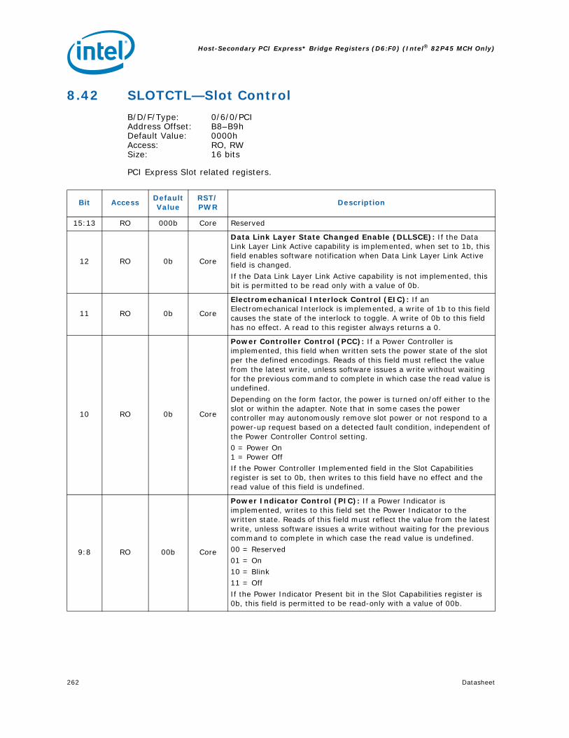
Host-Secondary PCI Express* Bridge Registers (D6:F0) (Intel® 82P45 MCH Only)
262 Datasheet
8.42 SLOTCTL—Slot Control
B/D/F/Type: 0/6/0/PCIAddress Offset: B8–B9hDefault Value: 0000hAccess: RO, RW Size: 16 bits
PCI Express Slot related registers.
Bit AccessDefault Value
RST/PWR
Description
15:13 RO 000b Core Reserved
12 RO 0b Core
Data Link Layer State Changed Enable (DLLSCE): If the Data Link Layer Link Active capability is implemented, when set to 1b, this field enables software notification when Data Link Layer Link Active field is changed.If the Data Link Layer Link Active capability is not implemented, this bit is permitted to be read only with a value of 0b.
11 RO 0b Core
Electromechanical Interlock Control (EIC): If an Electromechanical Interlock is implemented, a write of 1b to this field causes the state of the interlock to toggle. A write of 0b to this field has no effect. A read to this register always returns a 0.
10 RO 0b Core
Power Controller Control (PCC): If a Power Controller is implemented, this field when written sets the power state of the slot per the defined encodings. Reads of this field must reflect the value from the latest write, unless software issues a write without waiting for the previous command to complete in which case the read value is undefined.Depending on the form factor, the power is turned on/off either to the slot or within the adapter. Note that in some cases the power controller may autonomously remove slot power or not respond to a power-up request based on a detected fault condition, independent of the Power Controller Control setting.0 = Power On1 = Power OffIf the Power Controller Implemented field in the Slot Capabilities register is set to 0b, then writes to this field have no effect and the read value of this field is undefined.
9:8 RO 00b Core
Power Indicator Control (PIC): If a Power Indicator is implemented, writes to this field set the Power Indicator to the written state. Reads of this field must reflect the value from the latest write, unless software issues a write without waiting for the previous command to complete in which case the read value is undefined.00 = Reserved 01 = On 10 = Blink 11 = OffIf the Power Indicator Present bit in the Slot Capabilities register is 0b, this field is permitted to be read-only with a value of 00b.

Datasheet 263
Host-Secondary PCI Express* Bridge Registers (D6:F0) (Intel® 82P45 MCH Only)
7:6 RO 00b Core
Attention Indicator Control (AIC): If an Attention Indicator is implemented, writes to this field set the Attention Indicator to the written state.Reads of this field must reflect the value from the latest write, unless software issues a write without waiting for the previous command to complete in which case the read value is undefined. If the indicator is electrically controlled by chassis, the indicator is controlled directly by the downstream port through implementation specific mechanisms.00 = Reserved 01 = On 10 = Blink 11 = OffIf the Attention Indicator Present bit in the Slot Capabilities register is 0b, this field is permitted to be read only with a value of 00b.
5:4 RO 00b Core Reserved
3 RW 0b CorePresence Detect Changed Enable (PDCE): When set to 1b, this bit enables software notification on a presence detect changed event.
2 RO 0b Core
MRL Sensor Changed Enable (MSCE): When set to 1b, this bit enables software notification on a MRL sensor changed event.Default value of this field is 0b. If the MRL Sensor Present field in the Slot Capabilities register is set to 0b, this bit is permitted to be read-only with a value of 0b.
1 RO 0b Core
Power Fault Detected Enable (PFDE): When set to 1b, this bit enables software notification on a power fault event.Default value of this field is 0b. If Power Fault detection is not supported, this bit is permitted to be read-only with a value of 0b
0 RO 0b CoreButton Pressed Enable (ABPE): When set to 1b, this bit enables software notification on an attention button pressed event.
Bit AccessDefault Value
RST/PWR
Description

Host-Secondary PCI Express* Bridge Registers (D6:F0) (Intel® 82P45 MCH Only)
264 Datasheet
8.43 SLOTSTS—Slot Status
B/D/F/Type: 0/6/0/PCIAddress Offset: BA–BBhDefault Value: 0000hAccess: RO, RWC Size: 16 bits
PCI Express Slot related registers.
Bit AccessDefault Value
RST/PWR
Description
15:7 RO 0000000b Core Reserved
6 RO 0b Core
Presence Detect State (PDS): This bit indicates the presence of an adapter in the slot, reflected by the logical "OR" of the Physical Layer in-band presence detect mechanism and, if present, any out-of-band presence detect mechanism defined for the slot's corresponding form factor. Note that the in-band presence detect mechanism requires that power be applied to an adapter for its presence to be detected. 0 = Slot Empty1 = Card Present in SlotThis register must be implemented on all Downstream Ports that implement slots. For Downstream Ports not connected to slots (where the Slot Implemented bit of the PCI Express Capabilities Register is 0b), this bit must return 1b.
5:4 RO 00b Core Reserved
3 RWC 0b CoreDetect Changed (PDC): This bit is set when the value reported in Presence Detect State is changed.
2 RO 0b CoreMRL Sensor Changed (MSC): If an MRL sensor is implemented, this bit is set when a MRL Sensor state change is detected. If an MRL sensor is not implemented, this bit must not be set.
1 RO 0b Core
Power Fault Detected (PFD): If a Power Controller that supports power fault detection is implemented, this bit is set when the Power Controller detects a power fault at this slot. Note that, depending on hardware capability, it is possible that a power fault can be detected at any time, independent of the Power Controller Control setting or the occupancy of the slot. If power fault detection is not supported, this bit must not be set.
0 RO 0b CoreAttention Button Pressed (ABP): If an Attention Button is implemented, this bit is set when the attention button is pressed. If an Attention Button is not supported, this bit must not be set.

Datasheet 265
Host-Secondary PCI Express* Bridge Registers (D6:F0) (Intel® 82P45 MCH Only)
8.44 RCTL—Root Control
B/D/F/Type: 0/6/0/PCIAddress Offset: BC–BDhDefault Value: 0000hAccess: RO, RW Size: 16 bits
This register allows control of PCI Express Root Complex specific parameters. The system error control bits in this register determine if corresponding SERRs are generated when our device detects an error (reported in this device's Device Status register) or when an error message is received across the link. Reporting of SERR as controlled by these bits takes precedence over the SERR Enable in the PCI Command Register.
Bit AccessDefault Value
RST/PWR
Description
15:4 RO 000h Core Reserved
3 RW 0b Core
PME Interrupt Enable (PMEIE): 0 = No interrupts are generated as a result of receiving PME
messages.1 = Enables interrupt generation upon receipt of a PME message as
reflected in the PME Status bit of the Root Status Register. A PME interrupt is also generated if the PME Status bit of the Root Status Register is set when this bit is set from a cleared state.
2 RW 0b Core
System Error on Fatal Error Enable (SEFEE): This bit controls the Root Complex's response to fatal errors.0 = No SERR generated on receipt of fatal error.1 = Indicates that an SERR should be generated if a fatal error is
reported by any of the devices in the hierarchy associated with this Root Port, or by the Root Port itself.
1 RW 0b Core
System Error on Non-Fatal Uncorrectable Error Enable (SENFUEE): This bit controls the Root Complex's response to non-fatal errors.0 = No SERR generated on receipt of non-fatal error.1 = Indicates that an SERR should be generated if a non-fatal error is
reported by any of the devices in the hierarchy associated with this Root Port, or by the Root Port itself.
0 RW 0b Core
System Error on Correctable Error Enable (SECEE): This bit controls the Root Complex's response to correctable errors.0 = No SERR generated on receipt of correctable error.1 = Indicates that an SERR should be generated if a correctable error
is reported by any of the devices in the hierarchy associated with this Root Port, or by the Root Port itself.

Host-Secondary PCI Express* Bridge Registers (D6:F0) (Intel® 82P45 MCH Only)
266 Datasheet
8.45 RSTS—Root Status
B/D/F/Type: 0/6/0/PCIAddress Offset: C0–C3hDefault Value: 00000000hAccess: RO, RWC Size: 32 bits
This register provides information about PCI Express Root Complex specific parameters.
8.46 PELC—PCI Express Legacy Control
B/D/F/Type: 0/6/0/PCIAddress Offset: EC–EFhDefault Value: 00000000hAccess: RO, RW Size: 32 bits
This register controls functionality that is needed by Legacy (non-PCI Express aware) OSs during run time.
Bit AccessDefault Value
RST/PWR
Description
31:18 RO 0000h Core Reserved
17 RO 0b Core
PME Pending (PMEP): This bit indicates that another PME is pending when the PME Status bit is set. When the PME Status bit is cleared by software; the PME is delivered by hardware by setting the PME Status bit again and updating the Requestor ID appropriately. The PME pending bit is cleared by hardware if no more PMEs are pending.
16 RWC 0b Core
PME Status (PMES): This bit indicates that PME was asserted by the requestor ID indicated in the PME Requestor ID field. Subsequent PMEs are kept pending until the status register is cleared by writing a 1 to this field.
15:0 RO 0000h CorePME Requestor ID (PMERID): This field indicates the PCI requestor ID of the last PME requestor.
Bit AccessDefault Value
RST/PWR
Description
31:3 RO0000000
0hCore Reserved
2 RW 0b Core
PME GPE Enable (PMEGPE): 0 = Do not generate GPE PME message when PME is received.1 = Generate a GPE PME message when PME is received
(Assert_PMEGPE and Deassert_PMEGPE messages on DMI). This enables the MCH to support PMEs on the PCI Express port under legacy OSs.
1 RO 0b Core Reserved
0 RW 0b Core
General Message GPE Enable (GENGPE): 0 = Do not forward received GPE assert/de-assert messages.1 = Forward received GPE assert/de-assert messages. These general
GPE message can be received via the PCI Express port from an external Intel device and will be subsequently forwarded to the ICH (via Assert_GPE and Deassert_GPE messages on DMI).

Datasheet 267
Host-Secondary PCI Express* Bridge Registers (D6:F0) (Intel® 82P45 MCH Only)
8.47 VCECH—Virtual Channel Enhanced Capability Header
B/D/F/Type: 0/6/0/MMRAddress Offset: 100–103hDefault Value: 14010002hAccess: RO Size: 32 bits
This register indicates PCI Express device Virtual Channel capabilities. Extended capability structures for PCI Express devices are located in PCI Express extended configuration space and have different field definitions than standard PCI capability structures.
8.48 PVCCAP1—Port VC Capability Register 1
B/D/F/Type: 0/6/0/MMRAddress Offset: 104–107hDefault Value: 00000000hAccess: RO Size: 32 bits
This register describes the configuration of PCI Express Virtual Channels associated with this port.
Bit AccessDefault Value
RST/PWR
Description
31:20 RO 140h CorePointer to Next Capability (PNC): The Link Declaration Capability is the next in the PCI Express extended capabilities list.
19:16 RO 1h Core
PCI Express Virtual Channel Capability Version (PCIEVCCV): Hardwired to 1 to indicate compliances with the 1.1 version of the PCI Express specification.Note: This version does not change for 2.0 compliance.
15:0 RO 0002h CoreExtended Capability ID (ECID): Value of 0002h identifies this linked list item (capability structure) as being for PCI Express Virtual Channel registers.
Bit AccessDefault Value
RST/PWR
Description
31:7 RO 00000h Core Reserved
6:4 RO 000b Core
Low Priority Extended VC Count (LPEVCC): This field indicates the number of (extended) Virtual Channels in addition to the default VC belonging to the low-priority VC (LPVC) group that has the lowest priority with respect to other VC resources in a strict-priority VC Arbitration.The value of 0 in this field implies strict VC arbitration.
3 RO 0b Core Reserved
2:0 RO 000b CoreExtended VC Count (EVCC): This field indicates the number of (extended) Virtual Channels in addition to the default VC supported by the device.

Host-Secondary PCI Express* Bridge Registers (D6:F0) (Intel® 82P45 MCH Only)
268 Datasheet
8.49 PVCCAP2—Port VC Capability Register 2
B/D/F/Type: 0/6/0/MMRAddress Offset: 108–10BhDefault Value: 00000000hAccess: RO Size: 32 bits
This register describes the configuration of PCI Express Virtual Channels associated with this port.
8.50 PVCCTL—Port VC Control
B/D/F/Type: 0/6/0/MMRAddress Offset: 10C–10DhDefault Value: 0000hAccess: RO, RW Size: 16 bits
Bit AccessDefault Value
RST/PWR
Description
31:24 RO 00h Core
VC Arbitration Table Offset (VCATO): This field indicates the location of the VC Arbitration Table. This field contains the zero-based offset of the table in DQWORDS (16 bytes) from the base address of the Virtual Channel Capability Structure. A value of 0 indicates that the table is not present (due to fixed VC priority).
23:0 RO 0000h Core Reserved
Bit AccessDefault Value
RST/PWR
Description
15:4 RO 000h Core Reserved
3:1 RW 000b Core
VC Arbitration Select (VCAS): This field will be programmed by software to the only possible value as indicated in the VC Arbitration Capability field. Since there is no other VC supported than the default, this field is reserved.
0 RO 0b Core Reserved

Datasheet 269
Host-Secondary PCI Express* Bridge Registers (D6:F0) (Intel® 82P45 MCH Only)
8.51 VC0RCAP—VC0 Resource Capability
B/D/F/Type: 0/6/0/MMRAddress Offset: 110–113hDefault Value: 00000001hAccess: RO Size: 32 bits
Bit AccessDefault Value
RST/PWR
Description
31:16 RO 0000h Core Reserved
15 RO 0b Core
Reject Snoop Transactions (RSNPT): 0 = Transactions with or without the No Snoop bit set within the
Transaction Layer Packet header are allowed on this VC.1 = When Set, any transaction for which the No Snoop attribute is
applicable but is not Set within the TLP Header will be rejected as an Unsupported Request.
14:8 RO 0000h Core Reserved
7:0 RO 01h Core
Port Arbitration Capability: Indicates types of Port Arbitrationsupported by the VC resource. This field is valid for all Switch Ports, Root Ports that support peer-to-peer traffic, and RCRBs, but not for PCI Express Endpoint devices or Root Ports that do not support peer to peer traffic.Each bit location within this field corresponds to a Port Arbitration Capability defined below. When more than one bit in this field is Set, it indicates that the VC resource can be configured to provide different arbitration services.Software selects among these capabilities by writing to the Port Arbitration Select field (see below).Bit[0] = Default = 01b; Non-configurable hardware-fixed
arbitration scheme, e.g., Round Robin (RR)Bit[1] = Weighted Round Robin (WRR) arbitration with 32
phasesBit[2] = WRR arbitration with 64 phasesBit[3] = WRR arbitration with 128 phasesBit[4] = Time-based WRR with 128 phasesBit[5] = WRR arbitration with 256 phasesBits[6:7] = ReservedMCH default indicates "Non-configurable hardware-fixed arbitration scheme".

Host-Secondary PCI Express* Bridge Registers (D6:F0) (Intel® 82P45 MCH Only)
270 Datasheet
8.52 VC0RCTL—VC0 Resource Control
B/D/F/Type: 0/6/0/MMRAddress Offset: 114–117hDefault Value: 800000FFhAccess: RO, RW Size: 32 bits
This register controls the resources associated with PCI Express Virtual Channel 0.
Bit AccessDefault Value
RST/PWR
Description
31 RO 1b CoreVC0 Enable (VC0E): For VC0, this is hardwired to 1 and read only as VC0 can never be disabled.
30:27 RO 0h Core Reserved
26:24 RO 000b CoreVC0 ID (VC0ID): This field assigns a VC ID to the VC resource. For VC0 this is hardwired to 0 and read only.
23:20 RO 0000h Core Reserved
19:17 RW 000b Core
Port Arbitration Select: This field configures the VC resource to provide a particular Port Arbitration service. This field is valid for RCRBs, Root Ports that support peer to peer traffic, and Switch Ports, but not for PCI Express Endpoint devices or Root Ports that do not support peer to peer traffic.The permissible value of this field is a number corresponding to one of the asserted bits in the Port Arbitration Capability field of the VC resource.
16:8 RO 00h Core Reserved
7:1 RW 7Fh Core
TC/VC0 Map (TCVC0M): This field indicates the TCs (Traffic Classes) that are mapped to the VC resource. Bit locations within this field correspond to TC values. For example, when bit 7 is set in this field, TC7 is mapped to this VC resource. When more than one bit in this field is set, it indicates that multiple TCs are mapped to the VC resource. To remove one or more TCs from the TC/VC Map of an enabled VC, software must ensure that no new or outstanding transactions with the TC labels are targeted at the given Link.
0 RO 1b Core TC0/VC0 Map (TC0VC0M): Traffic Class 0 is always routed to VC0.

Datasheet 271
Host-Secondary PCI Express* Bridge Registers (D6:F0) (Intel® 82P45 MCH Only)
8.53 VC0RSTS—VC0 Resource Status
B/D/F/Type: 0/6/0/MMRAddress Offset: 11A–11BhDefault Value: 0002hAccess: RO Size: 16 bits
This register reports the Virtual Channel specific status.
8.54 RCLDECH—Root Complex Link Declaration Enhanced
B/D/F/Type: 0/6/0/MMRAddress Offset: 140–143hDefault Value: 00010005hAccess: RO Size: 32 bits
This capability declares links from this element (PCI Express) to other elements of the root complex component to which it belongs. See PCI Express specification for link/topology declaration requirements.
Bit AccessDefault Value
RST/PWR
Description
15:2 RO 0000h Core Reserved
1 RO 1b Core
VC0 Negotiation Pending (VC0NP): 0 = The VC negotiation is complete.1 = The VC resource is still in the process of negotiation (initialization
or disabling).This bit indicates the status of the process of Flow Control initialization. It is set by default on Reset, as well as whenever the corresponding Virtual Channel is Disabled or the Link is in the DL_Down state. It is cleared when the link successfully exits the FC_INIT2 state.Before using a Virtual Channel, software must check whether the VC Negotiation Pending fields for that Virtual Channel are cleared in both Components on a Link.
0 RO 0b Core Reserved
Bit AccessDefault Value
RST/PWR
Description
31:20 RO 000h CorePointer to Next Capability (PNC): This is the last capability in the PCI Express extended capabilities list.
19:16 RO 1h Core
Link Declaration Capability Version (LDCV): Hardwired to 1 to indicate compliances with the 1.1 version of the PCI Express specification.Note: This version does not change for 2.0 compliance.
15:0 RO 0005h CoreExtended Capability ID (ECID): Value of 0005h identifies this linked list item (capability structure) as being for PCI Express Link Declaration Capability.
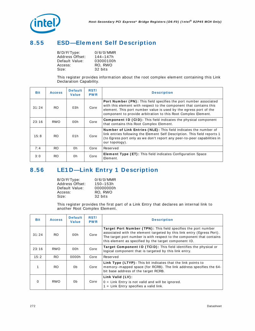
Host-Secondary PCI Express* Bridge Registers (D6:F0) (Intel® 82P45 MCH Only)
272 Datasheet
8.55 ESD—Element Self Description
B/D/F/Type: 0/6/0/MMRAddress Offset: 144–147hDefault Value: 03000100hAccess: RO, RWO Size: 32 bits
This register provides information about the root complex element containing this Link Declaration Capability.
8.56 LE1D—Link Entry 1 Description
B/D/F/Type: 0/6/0/MMRAddress Offset: 150–153hDefault Value: 00000000hAccess: RO, RWO Size: 32 bits
This register provides the first part of a Link Entry that declares an internal link to another Root Complex Element.
Bit AccessDefault Value
RST/PWR
Description
31:24 RO 03h Core
Port Number (PN): This field specifies the port number associated with this element with respect to the component that contains this element. This port number value is used by the egress port of the component to provide arbitration to this Root Complex Element.
23:16 RWO 00h CoreComponent ID (CID): This field indicates the physical component that contains this Root Complex Element.
15:8 RO 01h Core
Number of Link Entries (NLE): This field indicates the number of link entries following the Element Self Description. This field reports 1 (to Egress port only as we don't report any peer-to-peer capabilities in our topology).
7:4 RO 0h Core Reserved
3:0 RO 0h CoreElement Type (ET): This field indicates Configuration Space Element.
Bit AccessDefault Value
RST/PWR
Description
31:24 RO 00h Core
Target Port Number (TPN): This field specifies the port number associated with the element targeted by this link entry (Egress Port). The target port number is with respect to the component that contains this element as specified by the target component ID.
23:16 RWO 00h CoreTarget Component ID (TCID): This field identifies the physical or logical component that is targeted by this link entry.
15:2 RO 0000h Core Reserved
1 RO 0b CoreLink Type (LTYP): This bit indicates that the link points to memory–mapped space (for RCRB). The link address specifies the 64-bit base address of the target RCRB.
0 RWO 0b CoreLink Valid (LV): 0 = Link Entry is not valid and will be ignored.1 = Link Entry specifies a valid link.

Datasheet 273
Host-Secondary PCI Express* Bridge Registers (D6:F0) (Intel® 82P45 MCH Only)
8.57 LE1A—Link Entry 1 Address
B/D/F/Type: 0/6/0/MMRAddress Offset: 158–15FhDefault Value: 0000000000000000hAccess: RO, RWO Size: 64 bits
This register provides the second part of a Link Entry that declares an internal link to another Root Complex Element.
§ §
Bit AccessDefault Value
RST/PWR
Description
63:32 RO0000000
0hCore Reserved
31:12 RWO 00000h CoreLink Address (LA): This field provides the memory mapped base address of the RCRB that is the target element (Egress Port) for this link entry.
11:0 RO 000h Core Reserved

Host-Secondary PCI Express* Bridge Registers (D6:F0) (Intel® 82P45 MCH Only)
274 Datasheet

Datasheet 275
Integrated Graphics Registers (Device 2) (Intel® 82Q45, 82Q43, 82B43, 82G45, 82G43, 82G41 GMCH Only)
9 Integrated Graphics Registers (Device 2) (Intel® 82Q45, 82Q43, 82B43, 82G45, 82G43, 82G41 GMCH Only)
9.1 Integrated Graphics Registers (D2:F0)
Device 2 contains registers for the internal graphics functions. Table 15 lists the PCI configuration registers in order of ascending offset address.
Function 0 can be VGA compatible or not. This is selected through bit 1 of GGC register (Device 0, offset 52h).
Note: The following sections describe Device 2 PCI configuration registers only.
Table 15. Integrated Graphics Register Address Map (D2:F0)
Address Offset
Register Symbol
Register NameDefault Value
Access
0–1h VID2 Vendor Identification 8086h RO
2–3h DID2 Device Identificationsee register description
RO
4–5h PCICMD2 PCI Command 0000h RO, R/W
6–7h PCISTS2 PCI Status 0090h RO
8h RID2 Revision Identificationsee register description
RO
9–Bh CC Class Code 030000h RO
Ch CLS Cache Line Size 00h RO
Dh MLT2 Master Latency Timer 00h RO
Eh HDR2 Header Type 80h RO
10–17h GTTMMADRGraphics Translation Table, Memory Mapped Range Address
0000000000000004h
R/W, RO
18–1Fh GMADR Graphics Memory Range Address000000000000000Ch
R/W, RO, |R/W/L
20–23h IOBAR I/O Base Address 00000001h RO, R/W
2C–2Dh SVID2 Subsystem Vendor Identification 0000h R/WO
2E–2Fh SID2 Subsystem Identification 0000h R/WO
30–33h ROMADR Video BIOS ROM Base Address 00000000h RO
34h CAPPOINT Capabilities Pointer 90h RO
3Ch INTRLINE Interrupt Line 00h R/W
3Dh INTRPIN Interrupt Pin 01h RO
3Eh MINGNT Minimum Grant 00h RO

Integrated Graphics Registers (Device 2) (Intel® 82Q45, 82Q43, 82B43, 82G45, 82G43, 82G41GMCH Only)
276 Datasheet
3Fh MAXLAT Maximum Latency 00h RO
40–4Ch CAPID0 Capability Identifier000000000000000000010C0009h
RO
52–53h MGGC GMCH Graphics Control Register 0030h RO
54–57h DEVEN Device Enable 000023DBh RO
58–5Bh SSRW Software Scratch Read Write 00000000h R/W
5C–5Fh BSM Base of Stolen Memory 07800000h RO
60–61h HSRW Hardware Scratch Read Write 0000h R/W
92–93h MC Message Control 0000h RO, R/W
94–97h MA Message Address 00000000h R/W, RO
98–99h MD Message Data 0000h R/W
C0h GDRST Graphics Debug Reset 00hRO,
R/W/SC, R/W
D0–D1h PMCAPID Power Management Capabilities ID 0001h R/WO, RO
D2–D3h PMCAP Power Management Capabilities 0022h RO
D4–D5h PMCS Power Management Control/Status 0000h RO, R/W
E0–E1h SWSMI Software SMI 0000h R/W
Table 15. Integrated Graphics Register Address Map (D2:F0)
Address Offset
Register Symbol
Register NameDefault Value
Access

Datasheet 277
Integrated Graphics Registers (Device 2) (Intel® 82Q45, 82Q43, 82B43, 82G45, 82G43, 82G41 GMCH Only)
9.1.1 VID2—Vendor Identification
B/D/F/Type: 0/2/0/PCIAddress Offset: 0-1hDefault Value: 8086hAccess: ROSize: 16 bits
This register combined with the Device Identification register uniquely identifies any PCI device.
9.1.2 DID2—Device Identification
B/D/F/Type: 0/2/0/PCIAddress Offset: 2-3hDefault Value: see description belowAccess: ROSize: 16 bits
This register combined with the Vendor Identification register uniquely identifies any PCI device.
Bit AccessDefault Value
RST/PWR Description
15:0 RO 8086h CoreVendor Identification Number (VID): This field provides the PCI standard identification for Intel.
Bit AccessDefault Value
RST/PWR Description
15:0 ROsee
descriptionCore
Device Identification Number (DID): This field is an identifier assigned to the GMCH core/primary PCI device. Refer to the Intel® 4 Series Chipset Family Specification Update for values in this register.

Integrated Graphics Registers (Device 2) (Intel® 82Q45, 82Q43, 82B43, 82G45, 82G43, 82G41GMCH Only)
278 Datasheet
9.1.3 PCICMD2—PCI Command
B/D/F/Type: 0/2/0/PCIAddress Offset: 4-5hDefault Value: 0000hAccess: RO, R/WSize: 16 bits
This 16-bit register provides basic control over the IGD's ability to respond to PCI cycles. The PCICMD Register in the IGD disables the IGD PCI compliant master accesses to main memory.
Bit AccessDefault Value
RST/PWR Description
15:11 RO 00h Core Reserved
10 R/W 0b FLR, Core
Interrupt Disable (INTDIS): This bit disables the device from asserting INTx#.0 = Enable the assertion of this device's INTx# signal.1 = Disable the assertion of this device's INTx# signal.
DO_INTx messages will not be sent to DMI.
9 RO 0b CoreFast Back-to-Back (FB2B): Not Implemented. Hardwired to 0.
8 RO 0b CoreSERR Enable (SERRE): Not Implemented. Hardwired to 0.
7 RO 0b CoreAddress/Data Stepping Enable (ADSTEP): Not Implemented. Hardwired to 0.
6 RO 0b Core
Parity Error Enable (PERRE): Not Implemented. Hardwired to 0. Since the IGD belongs to the category of devices that does not corrupt programs or data in system memory or hard drives, the IGD ignores any parity error that it detects and continues with normal operation.
5 RO 0b CoreVideo Palette Snooping (VPS): This bit is hardwired to 0 to disable snooping.
4 RO 0b CoreMemory Write and Invalidate Enable (MWIE): Hardwired to 0. The IGD does not support memory write and invalidate commands.
3 RO 0b CoreSpecial Cycle Enable (SCE): This bit is hardwired to 0. The IGD ignores Special cycles.
2 R/W 0b FLR, CoreBus Master Enable (BME): 0 = Disable IGD bus mastering.1 = Enable the IGD to function as a PCI compliant master.
1 R/W 0b FLR, Core
Memory Access Enable (MAE): This bit controls the IGD's response to memory space accesses.0 = Disable.1 = Enable.
0 R/W 0b FLR, Core
I/O Access Enable (IOAE): This bit controls the IGD's response to I/O space accesses.0 = Disable.1 = Enable.

Datasheet 279
Integrated Graphics Registers (Device 2) (Intel® 82Q45, 82Q43, 82B43, 82G45, 82G43, 82G41 GMCH Only)
9.1.4 PCISTS2—PCI Status
B/D/F/Type: 0/2/0/PCIAddress Offset: 6-7hDefault Value: 0090hAccess: ROSize: 16 bits
PCISTS is a 16-bit status register that reports the occurrence of a PCI compliant master abort and PCI compliant target abort.
PCISTS also indicates the DEVSEL# timing that has been set by the IGD.
Bit AccessDefault Value
RST/PWR Description
15 RO 0b CoreDetected Parity Error (DPE): Since the IGD does not detect parity, this bit is always hardwired to 0.
14 RO 0b CoreSignaled System Error (SSE): The IGD never asserts SERR#, therefore this bit is hardwired to 0.
13 RO 0b CoreReceived Master Abort Status (RMAS): The IGD never gets a Master Abort, therefore this bit is hardwired to 0.
12 RO 0b CoreReceived Target Abort Status (RTAS): The IGD never gets a Target Abort, therefore this bit is hardwired to 0.
11 RO 0b CoreSignaled Target Abort Status (STAS): Hardwired to 0. The IGD does not use target abort semantics.
10:9 RO 00b CoreDEVSEL Timing (DEVT): N/A. These bits are hardwired to 00.
8 RO 0b CoreMaster Data Parity Error Detected (DPD): Since Parity Error Response is hardwired to disabled (and the IGD does not do any parity detection), this bit is hardwired to 0.
7 RO 1b CoreFast Back-to-Back (FB2B): Hardwired to 1. The IGD accepts fast back-to-back when the transactions are not to the same agent.
6 RO 0b Core User Defined Format (UDF): Hardwired to 0.
5 RO 0b Core 66 MHz PCI Capable (66C): N/A - Hardwired to 0.
4 RO 1b Core
Capability List (CLIST): This bit is set to 1 to indicate that the register at 34h provides an offset into the function's PCI Configuration Space containing a pointer to the location of the first item in the list.
3 RO 0b Core
Interrupt Status (INTSTS): This bit reflects the state of the interrupt in the device. Only when the Interrupt Disable bit in the command register is a 0 and this Interrupt Status bit is a 1, will the devices INTx# signal be asserted.
2:0 RO 000b Core Reserved

Integrated Graphics Registers (Device 2) (Intel® 82Q45, 82Q43, 82B43, 82G45, 82G43, 82G41GMCH Only)
280 Datasheet
9.1.5 RID2—Revision Identification
B/D/F/Type: 0/2/0/PCIAddress Offset: 8hDefault Value: see description belowAccess: ROSize: 8 bits
This register contains the revision number for Device 2, Functions 0 and 1.
9.1.6 CC—Class Code
B/D/F/Type: 0/2/0/PCIAddress Offset: 9-BhDefault Value: 030000hAccess: ROSize: 24 bits
This register contains the device programming interface information related to the Sub-Class Code and Base Class Code definition for the IGD. This register also contains the Base Class Code and the function sub-class in relation to the Base Class Code.
Bit AccessDefault Value
RST/PWR Description
7:0 RO see description
Core Revision Identification Number (RID): This is an 8-bit value that indicates the revision identification number for the GMCH Device 0. Refer to the Intel® 4 Series Chipset Family Specification Update for the value of this register.
Bit Access Default Value
RST/PWR
Description
23:16 RO 03h Core
Base Class Code (BCC): This is an 8-bit value that indicates the base class code for the GMCH. This code has the value 03h, indicating a Display Controller.When MCHBAR offset 44h, bit 31 is 0 this code has the value 03h, indicating a Display Controller.When MCHBAR offset 44, bit 31 is 1 this code has the value 04h, indicating a Multimedia Device.
15:8 RO 00h Core
Sub-Class Code (SUBCC): When MCHBAR offset 44 bit 31 is 0 this value will be determined based on Device 0 GGC register, GMS and IVD fields.00h = VGA compatible80h = Non VGA (GMS = "0000" or IVD = "1")When MCHBAR offset 44 bit 31 is 1 this value is 80h, indicating other multimedia device.
7:0 RO 00h Core
Programming Interface (PI): When MCHBAR offset 44, bit 31 is 0 this value is 00h, indicating a Display Controller.When MCHBAR offset 44, bit 31 is 1 this value is 00h, indicating a NOP.

Datasheet 281
Integrated Graphics Registers (Device 2) (Intel® 82Q45, 82Q43, 82B43, 82G45, 82G43, 82G41 GMCH Only)
9.1.7 CLS—Cache Line Size
B/D/F/Type: 0/2/0/PCIAddress Offset: ChDefault Value: 00hAccess: ROSize: 8 bits
The IGD does not support this register as a PCI slave.
9.1.8 MLT2—Master Latency Timer
B/D/F/Type: 0/2/0/PCIAddress Offset: DhDefault Value: 00hAccess: ROSize: 8 bits
The IGD does not support the programmability of the master latency timer because it does not perform bursts.
9.1.9 HDR2—Header Type
B/D/F/Type: 0/2/0/PCIAddress Offset: EhDefault Value: 80hAccess: ROSize: 8 bits
This register contains the Header Type of the IGD.
Bit AccessDefault Value
RST/PWR Description
7:0 RO 00h Core
Cache Line Size (CLS): This field is hardwired to 0s. The IGD as a PCI compliant master does not use the Memory Write and Invalidate command and, in general, does not perform operations based on cache line size.
Bit AccessDefault Value
RST/PWR Description
7:0 RO 00h CoreMaster Latency Timer Count Value (MLTCV): Hardwired to 0s.
Bit AccessDefault Value
RST/PWR Description
7 RO 1b Core
Multi Function Status (MFUNC): This bit indicates if the device is a Multi-Function Device. The Value of this register is determined by Device #0, offset 54h, DEVEN[4]. If Device 0 DEVEN[4] is set, the MFUNC bit is also set.
6:0 RO 00h CoreHeader Code (H): This is a 7-bit value that indicates the Header Code for the IGD. This code has the value 00h, indicating a type 0 configuration space format.

Integrated Graphics Registers (Device 2) (Intel® 82Q45, 82Q43, 82B43, 82G45, 82G43, 82G41GMCH Only)
282 Datasheet
9.1.10 GTTMMADR—Graphics Translation Table, Memory Mapped Range Address
B/D/F/Type: 0/2/0/PCIAddress Offset: 10-17hDefault Value: 0000000000000004hAccess: R/W, ROSize: 64 bits
This register requests allocation for combined Graphics Translation Table Modification Range and Memory Mapped Range. The space is 4 MB combined for MMIO and Global GTT table aperture (512 KB for MMIO and 2 MB for GTT). GTTADR will be at (GTTMMADR + 2 MB) while the MMIO base address will be the same as GTTMMADR.
For the Global GTT, this range is defined as a memory BAR in graphics device configuration space is an alias with which software is required to write values (PTEs) into and may also read values from the global Graphics Translation Table (GTT). PTEs cannot be written directly into the global GTT memory area.
The device snoops writes to this region in order to invalidate any cached translations within the various TLBs implemented on-chip. There are some exceptions to this.
The allocation is for 4 MB and the base address is defined by bits [35:22].
Bit AccessDefault Value
RST/PWR Description
63:36 R/W 0000000h FLR, Core(MBA): This field must be set to 0 since addressing above 64 GB is not supported.
35:22 R/W 0000h FLR, Core
Memory Base Address (MBA): This field is set by the OS, these bits correspond to address signals [35:22]. 4 MB combined for MMIO and Global GTT table aperture (512 KB for MMIO and 2 MB for GTT).
21:4 RO 00000h CoreReserved: Hardwired to 0s to indicate at least 4 MB address range.
3 RO 0b CorePrefetchable Memory (PREFMEM): Hardwired to 0 to prevent prefetching.
2:1 RO 10b Core
Memory Type (MEMTYP):00 = Indicates 32 bit base address01 = Reserved10 = Indicates 64 bit base address11 = Reserved
0 RO 0b CoreMemory/IO Space (MIOS): Hardwired to 0 to indicate memory space.

Datasheet 283
Integrated Graphics Registers (Device 2) (Intel® 82Q45, 82Q43, 82B43, 82G45, 82G43, 82G41 GMCH Only)
9.1.11 GMADR—Graphics Memory Range Address
B/D/F/Type: 0/2/0/PCIAddress Offset: 18-1FhDefault Value: 000000000000000ChAccess: R/W, RO, R/W/LSize: 64 bits
IGD graphics memory base address is specified in this register.
Bit AccessDefault Value
RST/PWR Description
63:36 R/W 0000000h FLR, CoreMemory Base Address (MBA2): This field is set by the OS, these bits correspond to address signals 63:36.
35:29 R/W 0000000b FLR, CoreMemory Base Address (MBA): This field is set by the OS, these bits correspond to address signals 35:29.
28 R/W/L 0b FLR, Core
512MB Address Mask (512ADMSK): This Bit is either part of the Memory Base Address (R/W) or part of the Address Mask (RO), depending on the value of MSAC[2:1].See MSAC (Device 2, Function 0, offset 62h) for details.
27 R/W/L 0b FLR, Core
256 MB Address Mask (256ADMSK): This bit is either part of the Memory Base Address (R/W) or part of the Address Mask (RO), depending on the value of MSAC[2:1]. See MSAC (Device 2, Function 0, offset 62h) for details.
26:4 RO 000000h CoreAddress Mask (ADM): Hardwired to 0s to indicate at least 128 MB address range.
3 RO 1b CorePrefetchable Memory (PREFMEM): Hardwired to 1 to enable prefetching.
2:1 RO 10b CoreMemory Type (MEMTYP): 00 = Indicates 32-bit address.10 = Indicates 64-bit address
0 RO 0b CoreMemory/IO Space (MIOS): Hardwired to 0 to indicate memory space.

Integrated Graphics Registers (Device 2) (Intel® 82Q45, 82Q43, 82B43, 82G45, 82G43, 82G41GMCH Only)
284 Datasheet
9.1.12 IOBAR—I/O Base Address
B/D/F/Type: 0/2/0/PCIAddress Offset: 20-23hDefault Value: 00000001hAccess: RO, R/WSize: 32 bits
This register provides the Base offset of the I/O registers within Device 2. Bits 15:3 are programmable allowing the I/O Base to be located anywhere in 16 bit I/O Address Space. Bits 2:1 are fixed and return zero, bit 0 is hardwired to a 1 indicating that 8 bytes of I/O space are decoded. Access to the 8Bs of I/O space is allowed in PM state D0 when IO Enable (PCICMD bit 0) set. Access is disallowed in PM states D1–D3 or if IO Enable is clear or if Device 2 is turned off or if internal graphics is disabled through the fuse or fuse override mechanisms.
Note that access to this IO BAR is independent of VGA functionality within Device 2. Also, note that this mechanism is available only through Function 0 of Device 2 and is not duplicated in Function 1.
If accesses to this IO bar is allowed then the GMCH claims all 8, 16, or 32 bit I/O cycles from the processor that falls within the 8B claimed.
9.1.13 SVID2—Subsystem Vendor Identification
B/D/F/Type: 0/2/0/PCIAddress Offset: 2C-2DhDefault Value: 0000hAccess: R/WOSize: 16 bits
Bit AccessDefault Value
RST/PWR Description
31:16 RO 0000h Core Reserved
15:3 R/W 0000h FLR, CoreIO Base Address (IOBASE): This field is set by the OS, these bits correspond to address signals 15:3.
2:1 RO 00b CoreMemory Type (MEMTYPE): Hardwired to 0s to indicate 32-bit address.
0 RO 1b CoreMemory/IO Space (MIOS): Hardwired to 1 to indicate I/O space.
Bit AccessDefault Value
RST/PWR Description
15:0 R/WO 0000h Core
Subsystem Vendor ID (SUBVID): This value is used to identify the vendor of the subsystem. This register should be programmed by BIOS during boot-up. Once written, this register becomes Read Only. This register can only be cleared by a Reset.

Datasheet 285
Integrated Graphics Registers (Device 2) (Intel® 82Q45, 82Q43, 82B43, 82G45, 82G43, 82G41 GMCH Only)
9.1.14 SID2—Subsystem Identification
B/D/F/Type: 0/2/0/PCIAddress Offset: 2E-2FhDefault Value: 0000hAccess: R/WOSize: 16 bits
9.1.15 ROMADR—Video BIOS ROM Base Address
B/D/F/Type: 0/2/0/PCIAddress Offset: 30-33hDefault Value: 00000000hAccess: ROSize: 32 bits
The IGD does not use a separate BIOS ROM, therefore this register is hardwired to 0s.
9.1.16 CAPPOINT—Capabilities Pointer
B/D/F/Type: 0/2/0/PCIAddress Offset: 34hDefault Value: 90hAccess: ROSize: 8 bits
Bit AccessDefault Value
RST/PWR Description
15:0 R/WO 0000h Core
Subsystem Identification (SUBID): This value is used to identify a particular subsystem. This field should be programmed by BIOS during boot-up. Once written, this register becomes Read Only. This register can only be cleared by a Reset.
Bit AccessDefault Value
RST/PWR Description
31:18 RO 0000h Core ROM Base Address (RBA): Hardwired to 0s.
17:11 RO 00h CoreAddress Mask (ADMSK): Hardwired to 0s to indicate 256 KB address range.
10:1 RO 000h Core Reserved: Hardwired to 0s.
0 RO 0b CoreROM BIOS Enable (RBE): 0 = ROM not accessible.
Bit AccessDefault Value
RST/PWR Description
7:0 RO 90h Core
Capabilities Pointer Value (CPV): This field contains an offset into the function's PCI Configuration Space for the first item in the New Capabilities Linked List, the MSI Capabilities ID registers at address 90h, or the Power Management capability at D0h.This value is determined by the configuration in CAPL[0].

Integrated Graphics Registers (Device 2) (Intel® 82Q45, 82Q43, 82B43, 82G45, 82G43, 82G41GMCH Only)
286 Datasheet
9.1.17 INTRLINE—Interrupt Line
B/D/F/Type: 0/2/0/PCIAddress Offset: 3ChDefault Value: 00hAccess: R/WSize: 8 bits
9.1.18 INTRPIN—Interrupt Pin
B/D/F/Type: 0/2/0/PCIAddress Offset: 3DhDefault Value: 01hAccess: ROSize: 8 bits
9.1.19 MINGNT—Minimum Grant
B/D/F/Type: 0/2/0/PCIAddress Offset: 3EhDefault Value: 00hAccess: ROSize: 8 bits
Bit AccessDefault Value
RST/PWR Description
7:0 R/W 00h Core
Interrupt Connection (INTCON): This field is used to communicate interrupt line routing information. POST software writes the routing information into this register as it initializes and configures the system. The value in this register indicates to which input of the system interrupt controller the device's interrupt pin is connected.
Bit AccessDefault Value
RST/PWR Description
7:0 RO 01h Core
Interrupt Pin (INTPIN): As a single function device, the IGD specifies INTA# as its interrupt pin.
01h = INTA#.
Bit AccessDefault Value
RST/PWR Description
7:0 RO 00h CoreMinimum Grant Value (MGV): The IGD does not burst as a PCI compliant master.
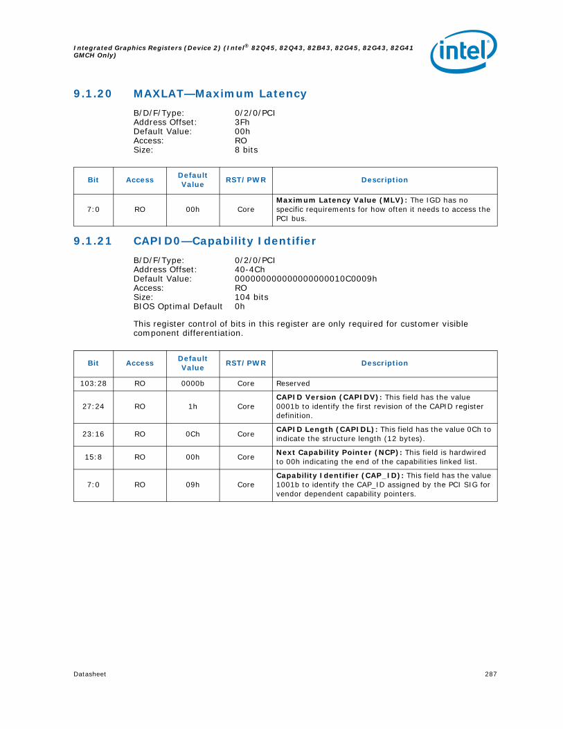
Datasheet 287
Integrated Graphics Registers (Device 2) (Intel® 82Q45, 82Q43, 82B43, 82G45, 82G43, 82G41 GMCH Only)
9.1.20 MAXLAT—Maximum Latency
B/D/F/Type: 0/2/0/PCIAddress Offset: 3FhDefault Value: 00hAccess: ROSize: 8 bits
9.1.21 CAPID0—Capability Identifier
B/D/F/Type: 0/2/0/PCIAddress Offset: 40-4ChDefault Value: 000000000000000000010C0009hAccess: ROSize: 104 bitsBIOS Optimal Default 0h
This register control of bits in this register are only required for customer visible component differentiation.
Bit AccessDefault Value
RST/PWR Description
7:0 RO 00h CoreMaximum Latency Value (MLV): The IGD has no specific requirements for how often it needs to access the PCI bus.
Bit AccessDefault Value
RST/PWR Description
103:28 RO 0000b Core Reserved
27:24 RO 1h CoreCAPID Version (CAPIDV): This field has the value 0001b to identify the first revision of the CAPID register definition.
23:16 RO 0Ch CoreCAPID Length (CAPIDL): This field has the value 0Ch to indicate the structure length (12 bytes).
15:8 RO 00h CoreNext Capability Pointer (NCP): This field is hardwired to 00h indicating the end of the capabilities linked list.
7:0 RO 09h CoreCapability Identifier (CAP_ID): This field has the value 1001b to identify the CAP_ID assigned by the PCI SIG for vendor dependent capability pointers.

Integrated Graphics Registers (Device 2) (Intel® 82Q45, 82Q43, 82B43, 82G45, 82G43, 82G41GMCH Only)
288 Datasheet
9.1.22 MGGC—GMCH Graphics Control Register
B/D/F/Type: 0/2/0/PCIAddress Offset: 52-53hDefault Value: 0030hAccess: ROSize: 16 bits
Note: All the bits in this register are locked in Intel TXT mode (82Q45/82Q43 GMCH only).
Bit AccessDefault Value
RST/PWR
Description
15:12 RO 0h Core Reserved
11:8 RO 0h Core
GTT Graphics Memory Size (GGMS): This field is used to select the amount of Main Memory that is pre-allocated to support the Internal Graphics Translation Table. The BIOS ensures that memory is pre-allocated only when Internal graphics is enabled.GSM is assumed to be a contiguous physical DRAM space with DSM, and BIOS needs to allocate a contiguous memory chunk. Hardware will drive the base of GSM from DSM only using the GSM size programmed in the register.0000 = No memory pre-allocated.0001 = No VT mode, 1 MB of memory pre-allocated for GTT.0011 = No VT mode, 2 MB of memory pre-allocated for GTT1001 = VT mode, 2 MB of memory pre-allocated for 1 MB of Global
GTT and 1 MB for Shadow GTT (82Q45, 82Q43 GMCH only)1010 = VT mode, 3 MB of memory pre-allocated for 1.5 MB of Global
GTT and 1.5 MB for Shadow GTT (82Q45 GMCH only)1011 VT mode, 4 MB of memory pre-allocated for 2 MB of Global
GTT and 2 MB for Shadow GTT (82Q45 GMCH only)
NOTE: All unspecified encodings of this register field are reserved, hardware functionality is not assured if used. This register is locked and becomes Read Only when the D_LCK bit in the SMRAM register is set.

Datasheet 289
Integrated Graphics Registers (Device 2) (Intel® 82Q45, 82Q43, 82B43, 82G45, 82G43, 82G41 GMCH Only)
7:4 RO 0011b Core
Graphics Mode Select (GMS): This field is used to select the amount of Main Memory that is pre-allocated to support the Internal Graphics device in VGA (non-linear) and Native (linear) modes. The BIOS ensures that memory is pre-allocated only when Internal graphics is enabled.
0000 = No memory pre-allocated. Device 2 (IGD) does not claim VGA cycles (Memory and I/O), and the Sub-Class Code field within Device 2, Function 0 Class Code register is 80h.0001 = Reserved0010 =Reserved0011 =Reserved0100 =Reserved0101 =DVMT (UMA) mode, 32 MB of memory pre-allocated for frame
buffer.0110 =DVMT (UMA) mode, 48 MB of memory pre-allocated for frame
buffer.0111 =DVMT (UMA) mode, 64 MB of memory pre-allocated for frame
buffer.1000 =DVMT (UMA) mode, 128 MB of memory pre-allocated for
frame buffer.1001 =DVMT (UMA) mode, 256 MB of memory pre-allocated for
frame buffer.1010 =DVMT (UMA) mode, 96 MB of memory pre-allocated (0 + 96).1011 =DVMT (UMA) mode, 160 MB of memory pre-allocated (64 +
96).1100 =DVMT (UMA) mode, 224 MB of memory pre-allocated (128 +
96).1101 =DVMT (UMA) mode, 352 MB of memory pre-allocated (256 +
96).
NOTE: This register is locked and becomes Read Only when the D_LCK bit in the SMRAM register is set.
Hardware does not clear or set any of these bits automatically based on IGD being disabled/enabled.BIOS Requirement: BIOS must not set this field to 000 if IVD (bit 1 of this register) is 0.
3:2 RO 00b Core Reserved
1 RO 0b Core
IGD VGA Disable (IVD): 0 = Enable. Device 2 (IGD) claims VGA memory and I/O cycles, the
Sub-Class Code within Device 2 Class Code register is 00h.1 = Disable. Device 2 (IGD) does not claim VGA cycles (Memory and
I/O), and the Sub- Class Code field within Device 2 function 0 Class Code register is 80h.
BIOS Requirement: BIOS must not set this bit to 0 if the GMS field (bits 6:4 of this register) pre-allocates no memory. This bit MUST be set to 1 if Device 2 is disabled either via a fuse or fuse override (CAPID0[38] = 1) or via a register (DEVEN[3] = 0).
0 RO 0b Core Reserved
Bit AccessDefault Value
RST/PWR
Description
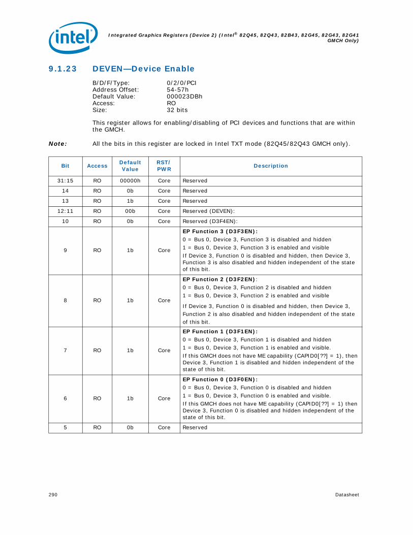
Integrated Graphics Registers (Device 2) (Intel® 82Q45, 82Q43, 82B43, 82G45, 82G43, 82G41GMCH Only)
290 Datasheet
9.1.23 DEVEN—Device Enable
B/D/F/Type: 0/2/0/PCIAddress Offset: 54-57hDefault Value: 000023DBhAccess: ROSize: 32 bits
This register allows for enabling/disabling of PCI devices and functions that are within the GMCH.
Note: All the bits in this register are locked in Intel TXT mode (82Q45/82Q43 GMCH only).
Bit AccessDefault Value
RST/PWR
Description
31:15 RO 00000h Core Reserved
14 RO 0b Core Reserved
13 RO 1b Core Reserved
12:11 RO 00b Core Reserved (DEVEN):
10 RO 0b Core Reserved (D3F4EN):
9 RO 1b Core
EP Function 3 (D3F3EN):0 = Bus 0, Device 3, Function 3 is disabled and hidden 1 = Bus 0, Device 3, Function 3 is enabled and visible If Device 3, Function 0 is disabled and hidden, then Device 3, Function 3 is also disabled and hidden independent of the state of this bit.
8 RO 1b Core
EP Function 2 (D3F2EN): 0 = Bus 0, Device 3, Function 2 is disabled and hidden 1 = Bus 0, Device 3, Function 2 is enabled and visible
If Device 3, Function 0 is disabled and hidden, then Device 3, Function 2 is also disabled and hidden independent of the state of this bit.
7 RO 1b Core
EP Function 1 (D3F1EN): 0 = Bus 0, Device 3, Function 1 is disabled and hidden1 = Bus 0, Device 3, Function 1 is enabled and visible. If this GMCH does not have ME capability (CAPID0[??] = 1), then Device 3, Function 1 is disabled and hidden independent of the state of this bit.
6 RO 1b Core
EP Function 0 (D3F0EN): 0 = Bus 0, Device 3, Function 0 is disabled and hidden 1 = Bus 0, Device 3, Function 0 is enabled and visible. If this GMCH does not have ME capability (CAPID0[??] = 1) then Device 3, Function 0 is disabled and hidden independent of the state of this bit.
5 RO 0b Core Reserved

Datasheet 291
Integrated Graphics Registers (Device 2) (Intel® 82Q45, 82Q43, 82B43, 82G45, 82G43, 82G41 GMCH Only)
4 RO 1b Core
Internal Graphics Engine Function 1 (D2F1EN): 0 = Bus 0, Device 2, Function 1 is disabled and hidden1 = Bus 0, Device 2, Function 1 is enabled and visibleIf Device 2, Function 0 is disabled and hidden, then Device 2, Function 1 is also disabled and hidden independent of the state of this bit.If this component is not capable of Dual Independent Display (CAPID0[78] = 1), then this bit is hardwired to 0b to hide Device 2, Function 1.
3 RO 1b Core
Internal Graphics Engine Function 0 (D2F0EN): 0 = Bus 0, Device 2, Function 0 is disabled and hidden1 = Bus 0, Device 2, Function 0 is enabled and visibleIf this GMCH does not have internal graphics capability (CAPID0[46] = 1), then Device 2, Function 0 is disabled and hidden independent of the state of this bit.
2 RO 0b Core Reserved
1 RO 1b Core
PCI Express Port (D1EN): 0 = Bus 0, Device 1, Function 0 is disabled and hidden. 1 = Bus 0, Device 1, Function 0 is enabled and visible.Default value is determined by the device capabilities (see CAPID0[44]), SDVO Presence hardware strap and the sDVO/PCIe Concurrent hardware strap. Device 1 is Disabled on Reset if the SDVO Presence strap was sampled high, and the sDVO/PCIe Concurrent strap was sampled low at the last assertion of PWROK, and is enabled by default otherwise.
0 RO 1b CoreHost Bridge (D0EN): Bus 0, Device 0, Function 0 may not be disabled and is therefore hardwired to 1.
Bit AccessDefault Value
RST/PWR
Description

Integrated Graphics Registers (Device 2) (Intel® 82Q45, 82Q43, 82B43, 82G45, 82G43, 82G41GMCH Only)
292 Datasheet
9.1.24 SSRW—Software Scratch Read Write
B/D/F/Type: 0/2/0/PCIAddress Offset: 58-5BhDefault Value: 00000000hAccess: R/WSize: 32 bits
9.1.25 BSM—Base of Stolen Memory
B/D/F/Type: 0/2/0/PCIAddress Offset: 5C-5FhDefault Value: 07800000hAccess: ROSize: 32 bits
Graphics Stolen Memory and TSEG are within DRAM space defined under TOLUD. From the top of low used DRAM, GMCH claims 1 to 64 MB of DRAM for internal graphics if enabled.
The base of stolen memory will always be below 4 GB. This is required to prevent aliasing between stolen range and the reclaim region.
9.1.26 HSRW—Hardware Scratch Read Write
B/D/F/Type: 0/2/0/PCIAddress Offset: 60-61hDefault Value: 0000hAccess: R/WSize: 16 bits
Bit AccessDefault Value
RST/PWR Description
31:0 R/W 00000000h FLR, Core Reserved
Bit AccessDefault Value
RST/PWR Description
31:20 RO 078h Core
Base of Stolen Memory (BSM): This register contains bits 31:20 of the base address of stolen DRAM memory. The host interface determines the base of Graphics Stolen memory by subtracting the graphics stolen memory size from TOLUD. See Device 0 TOLUD for more explanation.
19:0 RO 00000h Core Reserved
Bit AccessDefault Value
RST/PWR Description
15:0 R/W 0000h FLR, Core Reserved

Datasheet 293
Integrated Graphics Registers (Device 2) (Intel® 82Q45, 82Q43, 82B43, 82G45, 82G43, 82G41 GMCH Only)
9.1.27 MC—Message Control
B/D/F/Type: 0/2/0/PCIAddress Offset: 92-93hDefault Value: 0000hAccess: RO, R/WSize: 16 bits
System software can modify bits in this register, but the device is prohibited from doing so. If the device writes the same message multiple times, only one of those messages is assured to be serviced. If all of them must be serviced, the device must not generate the same message again until the driver services the earlier one.
9.1.28 MA—Message Address
B/D/F/Type: 0/2/0/PCIAddress Offset: 94-97hDefault Value: 00000000hAccess: R/W, ROSize: 32 bits
Bit AccessDefault Value
RST/PWR Description
15:8 RO 00h Core Reserved
7 RO 0b Core
64 Bit Capable (64BCAP): Hardwired to 0 to indicate that the function does not implement the upper 32 bits of the Message address register and is incapable of generating a 64-bit memory address.This may need to change in future implementations when addressable system memory exceeds the 32b/4 GB limit.
6:4 R/W 000b FLR, Core
Multiple Message Enable (MME): System software programs this field to indicate the actual number of messages allocated to this device. This number will be equal to or less than the number actually requested.The encoding is the same as for the MMC field below.
3:1 RO 000b Core
Multiple Message Capable (MMC): System Software reads this field to determine the number of messages being requested by this device.000 = 1All other encodings are reserved.
0 R/W 0b FLR, CoreMSI Enable (MSIEN): This bit controls the ability of this device to generate MSIs.
Bit AccessDefault Value
RST/PWR Description
31:2 R/W 00000000h FLR, Core
Message Address (MESSADD): This field is used by system software to assign an MSI address to the device.The device handles an MSI by writing the padded contents of the MD register to this address.
1:0 RO 00b CoreForce DWord Align (FDWORD): Hardwired to 0 so that addresses assigned by system software are always aligned on a DWord address boundary.

Integrated Graphics Registers (Device 2) (Intel® 82Q45, 82Q43, 82B43, 82G45, 82G43, 82G41GMCH Only)
294 Datasheet
9.1.29 MD—Message Data
B/D/F/Type: 0/2/0/PCIAddress Offset: 98-99hDefault Value: 0000hAccess: R/WSize: 16 bits
9.1.30 GDRST—Graphics Debug Reset
B/D/F/Type: 0/2/0/PCIAddress Offset: C0hDefault Value: 00hAccess: RO, R/W/SC, R/WSize: 8 bits
Bit AccessDefault Value
RST/PWR Description
15:0 R/W 0000h FLR, Core
Message Data (MESSDATA): This is the base message data pattern assigned by system software and used to handle an MSI from the device.When the device must generate an interrupt request, it writes a 32-bit value to the memory address specified in the MA register. The upper 16 bits are always set to 0. The lower 16 bits are supplied by this register.
Bit AccessDefault Value
RST/PWR Description
7:4 RO 0h FLR, Core Reserved
3:2 R/W 00b FLR, Core
Graphics Reset Domain (GRDOM): 00 = Full Graphics Reset will be performed (both render
and display clock domain resets asserted)01 = Render Only Reset (render clock domain reset
asserted)10 = Reserved (invalid Programming)11 = Media Only Reset (Media domain reset get asserted)
1 RO 0b FLR, Core Reserved
0 R/W/SC 0b FLR, Core
Graphics Reset Enable (GR): Setting this bit asserts graphics-only reset. The clock domains to be reset are determined by GRDOM. Hardware resets this bit when the reset is complete. Setting this bit without waiting for it to clear, is undefined behavior.Once this bit is set to a 1, all GFX core MMIO registers are returned to power on default state. All Ring buffer pointers are reset, command stream fetches are dropped and ongoing render pipeline processing is halted, state machines and State Variables returned to power on default state. If the Display is reset, all display engines are halted (garbage on screen). VGA memory is not available, Store DWords and interrupts are not ensured to be completed. Device 2 I/O registers are not available.Device 2 Configuration registers continue to be available while Graphics reset is asserted.This bit is hardwired auto-clear.

Datasheet 295
Integrated Graphics Registers (Device 2) (Intel® 82Q45, 82Q43, 82B43, 82G45, 82G43, 82G41 GMCH Only)
9.1.31 PMCAPID—Power Management Capabilities ID
B/D/F/Type: 0/2/0/PCIAddress Offset: D0-D1hDefault Value: 0001hAccess: R/WO, ROSize: 16 bits
9.1.32 PMCAP—Power Management Capabilities
B/D/F/Type: 0/2/0/PCIAddress Offset: D2-D3hDefault Value: 0022hAccess: ROSize: 16 bits
This register is a Mirror of Function 0 with the same read/write attributes. The hardware implements a single physical register common to both Functions 0 and 1.
Bit AccessDefault Value
RST/PWR Description
15:8 R/WO 00h Core
Next Capability Pointer (NEXT_PTR): This field contains a pointer to the next item in the capabilities list. BIOS is responsible for writing this to the FLR Capability when applicable.
7:0 RO 01h CoreCapability Identifier (CAP_ID): SIG defines this ID is 01h for power management.
Bit AccessDefault Value
RST/PWR Description
15:11 RO 00h CorePME Support (PMES): This field indicates the power states in which the IGD may assert PME#. Hardwired to 0 to indicate that the IGD does not assert the PME# signal.
10 RO 0b CoreD2 Support (D2): The D2 power management state is not supported. This bit is hardwired to 0.
9 RO 0b CoreD1 Support (D1): Hardwired to 0 to indicate that the D1 power management state is not supported.
8:6 RO 000b Core Reserved
5 RO 1b CoreDevice Specific Initialization (DSI): Hardwired to 1 to indicate that special initialization of the IGD is required before generic class device driver is to use it.
4 RO 0b Core Reserved
3 RO 0b CorePME Clock (PMECLK): Hardwired to 0 to indicate IGD does not support PME# generation.
2:0 RO 010b Core
Version (VER): Hardwired to 010b to indicate that there are 4 bytes of power management registers implemented and that this device complies with the PCI Power Management Interface Specification, Revision 1.1.

Integrated Graphics Registers (Device 2) (Intel® 82Q45, 82Q43, 82B43, 82G45, 82G43, 82G41GMCH Only)
296 Datasheet
9.1.33 PMCS—Power Management Control/Status
B/D/F/Type: 0/2/0/PCIAddress Offset: D4-D5hDefault Value: 0000hAccess: RO, R/WSize: 16 bits
9.1.34 SWSMI—Software SMI
B/D/F/Type: 0/2/0/PCIAddress Offset: E0-E1hDefault Value: 0000hAccess: R/WSize: 16 bits
As long as there is the potential that DVO port legacy drivers exist which expect this register at this address, Device 2, Function 0 address E0h–E1h must be reserved for this register.
Bit AccessDefault Value
RST/PWR
Description
15 RO 0b CorePME Status (PMESTS): This bit is 0 to indicate that IGD does not support PME# generation from D3 (cold).
14:13 RO 00b CoreData Scale (DSCALE): The IGD does not support data register. This bit always returns 00 when read, write operations have no effect.
12:9 RO 0h CoreData Select (DSEL): The IGD does not support data register. This bit always returns 0h when read, write operations have no effect.
8 RO 0b CorePME Enable (PME_EN): This bit is 0 to indicate that PME# assertion from D3 (cold) is disabled.
7:2 RO 00h Core Reserved
1:0 R/W 00bFLR, Core
Power State (PWRSTAT): This field indicates the current power state of the IGD and can be used to set the IGD into a new power state. If software attempts to write an unsupported state to this field, write operation must complete normally on the bus, but the data is discarded and no state change occurs. On a transition from D3 to D0 the graphics controller is optionally reset to initial values. 00 = D0 (Default)01 = D1 (Not Supported)10 = D2 (Not Supported)11 = D3
Bit AccessDefault Value
RST/PWR Description
15:8 R/W 00h Core Software Scratch Bits (SWSB):
7:1 R/W 00h CoreSoftware Flag (SWF): This field is used to indicate caller and SMI function desired, as well as return result.
0 R/W 0b CoreGMCH Software SMI Event (GSSMIE): When set, this bit will trigger an SMI. Software must write a 0 to clear this bit.

Datasheet 297
Integrated Graphics Registers (Device 2) (Intel® 82Q45, 82Q43, 82B43, 82G45, 82G43, 82G41 GMCH Only)
9.2 Integrated Graphics Registers (D2:F1)
Table 16. PCI Register Address Map (D2:F1)
Address Offset
Register Symbol
Register NameDefault Value
Access
0–1h VID2 Vendor Identification 8086h RO
2–3h DID2 Device Identificationsee register description
RO
4–5h PCICMD2 PCI Command 0000h RO, R/W
6–7h PCISTS2 PCI Status 0090h RO
8h RID2 Revision Identificationsee register description
RO
9–Bh CC Class Code Register 038000h RO
Ch CLS Cache Line Size 00h RO
Dh MLT2 Master Latency Timer 00h RO
Eh HDR2 Header Type 80h RO
10–17h MMADR Memory Mapped Range Address0000000000
000004hR/W, RO
2C–2Dh SVID2 Subsystem Vendor Identification 0000h RO
2E–2Fh SID2 Subsystem Identification 0000h RO
30–33h ROMADR Video BIOS ROM Base Address 00000000h RO
34h CAPPOINT Capabilities Pointer D0h RO
3Eh MINGNT Minimum Grant 00h RO
3Fh MAXLAT Maximum Latency 00h RO
40–4Ch CAPID0 Mirror of Dev0 Capability Identifier00000000000000000001
0C0009hRO
52–53h MGGCMirror of Device 0 GMCH Graphics Control Register
0030h RO
54–57h DEVEN Device Enable 000023DBh RO
58–5Bh SSRWMirror of Function 0 Software Scratch Read Write
00000000h RO
5C–5Fh BSM Mirror of Function 0 Base of Stolen Memory 07800000h RO
60–61h HSRWMirror of Device 2 Function 0 Hardware Scratch Read Write
0000h RO
C0h GDRSTMirror of Device 2 Function 0 Graphics Reset
00h RO
D0–D1h PMCAPIDMirror of Function 0 Power Management Capabilities ID
0001h R/WO, RO
D2–D3h PMCAPMirror of Function 0 Power Management Capabilities
0022h RO
D4–D5h PMCS Power Management Control/Status 0000h RO, R/W
D8–DBh — Reserved 00000000h RO
E0–E1h SWSMI Mirror of Func0 Software SMI 0000h RO

Integrated Graphics Registers (Device 2) (Intel® 82Q45, 82Q43, 82B43, 82G45, 82G43, 82G41GMCH Only)
298 Datasheet
9.2.1 VID2—Vendor Identification
B/D/F/Type: 0/2/1/PCIAddress Offset: 0-1hDefault Value: 8086hAccess: ROSize: 16 bits
This register combined with the Device Identification register uniquely identifies any PCI device.
9.2.2 DID2—Device Identification
B/D/F/Type: 0/2/1/PCIAddress Offset: 2-3hDefault Value: see description belowAccess: ROSize: 16 bits
This register is unique in Function 1 (the Function 0 DID is separate). This difference in Device ID is necessary for allowing distinct Plug and Play enumeration of function 1 when both function 0 and function 1 have the same class code.
Bit AccessDefault Value
RST/PWR Description
15:0 RO 8086h CoreVendor Identification Number (VID): PCI standard identification for Intel.
Bit AccessDefault Value
RST/PWR Description
15:0 ROsee
descriptionCore
Device Identification Number (DID): Identifier assigned to the GMCH core/primary PCI device. Refer to the Intel® 4 Series Chipset Family Specification Update for values in this register.

Datasheet 299
Integrated Graphics Registers (Device 2) (Intel® 82Q45, 82Q43, 82B43, 82G45, 82G43, 82G41 GMCH Only)
9.2.3 PCICMD2—PCI Command
B/D/F/Type: 0/2/1/PCIAddress Offset: 4-5hDefault Value: 0000hAccess: RO, R/WSize: 16 bits
This 16-bit register provides basic control over the IGD's ability to respond to PCI cycles. The PCICMD Register in the IGD disables the IGD PCI compliant master accesses to main memory.
Bit AccessDefault Value
RST/PWR Description
15:10 RO 00h Core Reserved
9 RO 0b CoreFast Back-to-Back (FB2B): Not Implemented. Hardwired to 0.
8 RO 0b CoreSERR Enable (SERRE): Not Implemented. Hardwired to 0.
7 RO 0b CoreAddress/Data Stepping Enable (ADSTEP): Not Implemented. Hardwired to 0.
6 RO 0b Core
Parity Error Enable (PERRE): Not Implemented. Hardwired to 0. Since the IGD belongs to the category of devices that does not corrupt programs or data in system memory or hard drives, the IGD ignores any parity error that it detects and continues with normal operation.
5 RO 0b CoreVGA Palette Snoop Enable (VGASNOOP): This bit is hardwired to 0 to disable snooping.
4 RO 0b CoreMemory Write and Invalidate Enable (MWIE): Hardwired to 0. The IGD does not support memory write and invalidate commands.
3 RO 0b CoreSpecial Cycle Enable (SCE): This bit is hardwired to 0. The IGD ignores Special cycles.
2 R/W 0b FLR, CoreBus Master Enable (BME): 0 = Disable IGD bus mastering.1 = Enable the IGD to function as a PCI compliant master.
1 R/W 0b FLR, Core
Memory Access Enable (MAE): This bit controls the IGD's response to memory space accesses.0 = Disable.1 = Enable.
0 R/W 0b FLR, Core
I/O Access Enable (IOAE): This bit controls the IGD's response to I/O space accesses.0 = Disable.1 = Enable.

Integrated Graphics Registers (Device 2) (Intel® 82Q45, 82Q43, 82B43, 82G45, 82G43, 82G41GMCH Only)
300 Datasheet
9.2.4 PCISTS2—PCI Status
B/D/F/Type: 0/2/1/PCIAddress Offset: 6-7hDefault Value: 0090hAccess: ROSize: 16 bits
PCISTS is a 16-bit status register that reports the occurrence of a PCI compliant master abort and PCI compliant target abort. PCISTS also indicates the DEVSEL# timing that has been set by the IGD.
Bit AccessDefault Value
RST/PWR Description
15 RO 0b CoreDetected Parity Error (DPE): Since the IGD does not detect parity, this bit is always hardwired to 0.
14 RO 0b CoreSignaled System Error (SSE): The IGD never asserts SERR#, therefore this bit is hardwired to 0.
13 RO 0b CoreReceived Master Abort Status (RMAS): The IGD never gets a Master Abort, therefore this bit is hardwired to 0.
12 RO 0b CoreReceived Target Abort Status (RTAS): The IGD never gets a Target Abort, therefore this bit is hardwired to 0.
11 RO 0b CoreSignaled Target Abort Status (STAS): Hardwired to 0. The IGD does not use target abort semantics.
10:9 RO 00b CoreDEVSEL Timing (DEVT): N/A. These bits are hardwired to "00".
8 RO 0b CoreMaster Data Parity Error Detected (DPD): Since Parity Error Response is hardwired to disabled (and the IGD does not do any parity detection), this bit is hardwired to 0.
7 RO 1b CoreFast Back-to-Back (FB2B): Hardwired to 1. The IGD accepts fast back-to-back when the transactions are not to the same agent.
6 RO 0b Core User Defined Format (UDF): Hardwired to 0.
5 RO 0b Core 66 MHz PCI Capable (66C): N/A - Hardwired to 0.
4 RO 1b Core
Capability List (CLIST): This bit is set to 1 to indicate that the register at 34h provides an offset into the function's PCI Configuration Space containing a pointer to the location of the first item in the list.
3 RO 0b Core Interrupt Status (INTSTS): Hardwired to 0.
2:0 RO 000b Core Reserved

Datasheet 301
Integrated Graphics Registers (Device 2) (Intel® 82Q45, 82Q43, 82B43, 82G45, 82G43, 82G41 GMCH Only)
9.2.5 RID2—Revision Identification
B/D/F/Type: 0/2/1/PCIAddress Offset: 8hDefault Value: see description belowAccess: ROSize: 8 bits
This register contains the revision number for Device #2 Functions 0 and 1
9.2.6 CC—Class Code Register
B/D/F/Type: 0/2/1/PCIAddress Offset: 9-BhDefault Value: 038000hAccess: ROSize: 24 bits
This register contains the device programming interface information related to the Sub-Class Code and Base Class Code definition for the IGD. This register also contains the Base Class Code and the function sub-class in relation to the Base Class Code.
Bit AccessDefault Value
RST/PWR Description
7:0 ROsee
descriptionCore
Revision Identification Number (RID): This is an 8-bit value that indicates the revision identification number for the GMCH Device 0. Refer to the Intel® 4 Series Chipset Family Specification Update for the value of this register.
Bit AccessDefault Value
RST/PWR Description
23:16 RO 03h Core
Base Class Code (BCC): This is an 8-bit value that indicates the base class code for the GMCH. This code has the value 03h, indicating a Display Controller.When MCHBAR offset 44h, bit 31 is 0 this code has the value 03h, indicating a Display Controller.When MCHBAR offset 44h, bit 31 is 1 this code has the value 04h, indicating a Multimedia Device.
15:8 RO 80h Core
Sub-Class Code (SUBCC): When MCHBAR offset 44, bit 31 is 0 this value 80h, indicating Non VGA.When MCHBAR offset 44h, bit 31 is 1 this value is 80h, indicating other multimedia device.
7:0 RO 00h Core
Programming Interface (PI): When MCHBAR offset 44h, bit 31 is 0 this value is 00h, indicating a Display Controller.When MCHBAR offset 44h, bit 31 is 1 this value is 00h, indicating a NOP.

Integrated Graphics Registers (Device 2) (Intel® 82Q45, 82Q43, 82B43, 82G45, 82G43, 82G41GMCH Only)
302 Datasheet
9.2.7 CLS—Cache Line Size
B/D/F/Type: 0/2/1/PCIAddress Offset: ChDefault Value: 00hAccess: ROSize: 8 bits
The IGD does not support this register as a PCI slave.
9.2.8 MLT2—Master Latency Timer
B/D/F/Type: 0/2/1/PCIAddress Offset: DhDefault Value: 00hAccess: ROSize: 8 bits
The IGD does not support the programmability of the master latency timer because it does not perform bursts.
9.2.9 HDR2—Header Type
B/D/F/Type: 0/2/1/PCIAddress Offset: EhDefault Value: 80hAccess: ROSize: 8 bits
This register contains the Header Type of the IGD.
Bit AccessDefault Value
RST/PWR Description
7:0 RO 00h Core
Cache Line Size (CLS): This field is hardwired to 0s. The IGD as a PCI compliant master does not use the Memory Write and Invalidate command and, in general, does not perform operations based on cache line size.
Bit AccessDefault Value
RST/PWR Description
7:0 RO 00h CoreMaster Latency Timer Count Value (MLTCV): Hardwired to 0s.
Bit AccessDefault Value
RST/PWR Description
7 RO 1b Core
Multi Function Status (MFUNC): This bit indicates if the device is a Multi-Function Device. The Value of this register is determined by Device 0, offset 54h, DEVEN[4]. If Device 0 DEVEN[4] is set, the MFUNC bit is also set.
6:0 RO 00h CoreHeader Code (H): This is an 7-bit value that indicates the Header Code for the IGD. This code has the value 00h, indicating a type 0 configuration space format.

Datasheet 303
Integrated Graphics Registers (Device 2) (Intel® 82Q45, 82Q43, 82B43, 82G45, 82G43, 82G41 GMCH Only)
9.2.10 MMADR—Memory Mapped Range Address
B/D/F/Type: 0/2/1/PCIAddress Offset: 10-17hDefault Value: 0000000000000004hAccess: R/W, ROSize: 64 bits
This register requests allocation for the IGD registers and instruction ports. The allocation is for 512 KB and the base address is defined by bits [31:19].
9.2.11 SVID2—Subsystem Vendor Identification
B/D/F/Type: 0/2/1/PCIAddress Offset: 2C-2DhDefault Value: 0000hAccess: ROSize: 16 bits
Bit AccessDefault Value
RST/PWR Description
63:36 R/W 0000000h FLR, Core Reserved
35:20 R/W 0000h FLR, CoreMemory Base Address (MBA): Set by the OS, these bits correspond to address signals 35:20.
19:4 RO 0000h CoreAddress Mask (ADMSK): Hardwired to 0s to indicate 512 KB address range (aligned to 1 MB boundary).
3 RO 0b CorePrefetchable Memory (PREFMEM): Hardwired to 0 to prevent prefetching.
2:1 RO 10b CoreMemory Type (MEMTYP): Hardwired to 10b to indicate 64-bit address.
0 RO 0b CoreMemory / IO Space (MIOS): Hardwired to 0 to indicate memory space.
Bit AccessDefault Value
RST/PWR Description
15:0 RO 0000h Core
Subsystem Vendor ID (SUBVID): This value is used to identify the vendor of the subsystem. This register should be programmed by BIOS during boot-up. Once written, this register becomes Read Only.This register can only be cleared by a Reset.

Integrated Graphics Registers (Device 2) (Intel® 82Q45, 82Q43, 82B43, 82G45, 82G43, 82G41GMCH Only)
304 Datasheet
9.2.12 SID2—Subsystem Identification
B/D/F/Type: 0/2/1/PCIAddress Offset: 2E-2FhDefault Value: 0000hAccess: ROSize: 16 bits
9.2.13 ROMADR—Video BIOS ROM Base Address
B/D/F/Type: 0/2/1/PCIAddress Offset: 30-33hDefault Value: 00000000hAccess: ROSize: 32 bits
The IGD does not use a separate BIOS ROM, therefore this register is hardwired to 0s.
9.2.14 CAPPOINT—Capabilities Pointer
B/D/F/Type: 0/2/1/PCIAddress Offset: 34hDefault Value: D0hAccess: ROSize: 8 bits
Bit AccessDefault Value
RST/PWR Description
15:0 RO 0000h Core
Subsystem Identification (SUBID): This value is used to identify a particular subsystem. This field should be programmed by BIOS during boot-up. Once written, this register becomes Read Only. This register can only be cleared by a Reset.
Bit AccessDefault Value
RST/PWR Description
31:18 RO 0000h Core ROM Base Address (RBA): Hardwired to 0s.
17:11 RO 00h CoreAddress Mask (ADMSK): Hardwired to 0s to indicate 256 KB address range.
10:1 RO 000h Core Reserved: Hardwired to 0s.
0 RO 0b CoreROM BIOS Enable (RBE): 0 = ROM not accessible.
Bit AccessDefault Value
RST/PWR Description
7:0 RO D0h Core
Capabilities Pointer Value (CPV): This field contains an offset into the function's PCI Configuration Space for the first item in the New Capabilities Linked List, the Power Management capability at D0h.
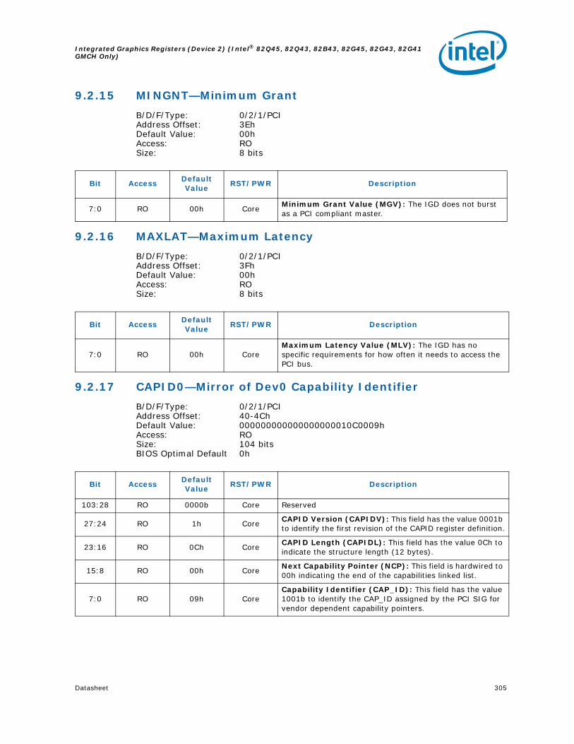
Datasheet 305
Integrated Graphics Registers (Device 2) (Intel® 82Q45, 82Q43, 82B43, 82G45, 82G43, 82G41 GMCH Only)
9.2.15 MINGNT—Minimum Grant
B/D/F/Type: 0/2/1/PCIAddress Offset: 3EhDefault Value: 00hAccess: ROSize: 8 bits
9.2.16 MAXLAT—Maximum Latency
B/D/F/Type: 0/2/1/PCIAddress Offset: 3FhDefault Value: 00hAccess: ROSize: 8 bits
9.2.17 CAPID0—Mirror of Dev0 Capability Identifier
B/D/F/Type: 0/2/1/PCIAddress Offset: 40-4ChDefault Value: 000000000000000000010C0009hAccess: ROSize: 104 bitsBIOS Optimal Default 0h
Bit AccessDefault Value
RST/PWR Description
7:0 RO 00h CoreMinimum Grant Value (MGV): The IGD does not burst as a PCI compliant master.
Bit AccessDefault Value
RST/PWR Description
7:0 RO 00h CoreMaximum Latency Value (MLV): The IGD has no specific requirements for how often it needs to access the PCI bus.
Bit AccessDefault Value
RST/PWR Description
103:28 RO 0000b Core Reserved
27:24 RO 1h CoreCAPID Version (CAPIDV): This field has the value 0001b to identify the first revision of the CAPID register definition.
23:16 RO 0Ch CoreCAPID Length (CAPIDL): This field has the value 0Ch to indicate the structure length (12 bytes).
15:8 RO 00h CoreNext Capability Pointer (NCP): This field is hardwired to 00h indicating the end of the capabilities linked list.
7:0 RO 09h CoreCapability Identifier (CAP_ID): This field has the value 1001b to identify the CAP_ID assigned by the PCI SIG for vendor dependent capability pointers.

Integrated Graphics Registers (Device 2) (Intel® 82Q45, 82Q43, 82B43, 82G45, 82G43, 82G41GMCH Only)
306 Datasheet
9.2.18 MGGC—Mirror of Device 0 GMCH Graphics Control Register
B/D/F/Type: 0/2/1/PCIAddress Offset: 52-53hDefault Value: 0030hAccess: ROSize: 16 bits
Note: All the bits in this register are locked in Intel TXT mode (82Q45/82Q43 GMCH only).
Bit AccessDefault Value
RST/PWR
Description
15:12 RO 0h Core Reserved
11:8 RO 0h Core
GTT Graphics Memory Size (GGMS): This field is used to select the amount of Main Memory that is pre-allocated to support the Internal Graphics Translation Table. The BIOS ensures that memory is pre-allocated only when Internal graphics is enabled.GSM is assumed to be a contiguous physical DRAM space with DSM, and BIOS needs to allocate a contiguous memory chunk. Hardware will drive the base of GSM from DSM only using the GSM size programmed in the register.
0000 = No memory pre-allocated.0001 = No VT mode, 1 MB of memory pre-allocated for GTT.0011 = No VT mode, 2 MB of memory pre-allocated for GTT1001 = VT mode, 2 MB of memory pre-allocated for 1 MB of Global GTT and
1 MB for Shadow GTT (82Q45 GMCH only)1010 = VT mode, 3 MB of memory pre-allocated for 1.5 MB of Global GTT
and 1.5 MB for Shadow GTT (82Q45 GMCH only)1011 = VT mode, 4 MB of memory pre-allocated for 2 MB of Global GTT and
2 MB for Shadow GTT (82Q45 GMCH only)
NOTE: All unspecified encodings of this register field are reserved; hardware functionality is not ensured if used. This register is locked and becomes Read Only when the D_LCK bit in the SMRAM register is set.

Datasheet 307
Integrated Graphics Registers (Device 2) (Intel® 82Q45, 82Q43, 82B43, 82G45, 82G43, 82G41 GMCH Only)
7:4 RO 0011b Core
Graphics Mode Select (GMS): This field is used to select the amount of Main Memory that is pre-allocated to support the Internal Graphics device in VGA (non-linear) and Native (linear) modes. The BIOS ensures that memory is pre-allocated only when Internal graphics is enabled.0000 = No memory pre-allocated. Device 2 (IGD) does not claim VGA
cycles (Memory and I/O), and the Sub-Class Code field within Device 2, function 0 Class Code register is 80h.
0001 = Reserved0010 = Reserved0011 = Reserved0100 = Reserved0101 = DVMT (UMA) mode, 32 MB of memory pre-allocated for frame
buffer.0110 = DVMT (UMA) mode, 48 MB of memory pre-allocated for frame
buffer.0111 = DVMT (UMA) mode, 64 MB of memory pre-allocated for frame
buffer.1000 = DVMT (UMA) mode, 128 MB of memory pre-allocated for frame
buffer.1001 = DVMT (UMA) mode, 256 MB of memory pre-allocated for frame
buffer.1010 = DVMT (UMA) mode, 96 MB of memory pre-allocated (0 + 96).1011 = DVMT (UMA) mode, 160 MB of memory pre-allocated (64 + 96).1100 = DVMT (UMA) mode, 224 MB of memory pre-allocated (128 + 96).1101 = DVMT (UMA) mode, 352 MB of memory pre-allocated (256 + 96).
NOTE: This register is locked and becomes Read Only when the D_LCK bit in the SMRAM register is set.
Hardware does not clear or set any of these bits automatically based on IGD being disabled/enabled.BIOS Requirement: BIOS must not set this field to 000 if IVD (bit 1 of this register) is 0.
3:2 RO 00b Core Reserved
1 RO 0b Core
IGD VGA Disable (IVD): 0 = Enable. Device 2 (IGD) claims VGA memory and I/O cycles, and the
Sub-Class Code within Device 2 Class Code register is 00h.1 = Disable. Device 2 (IGD) does not claim VGA cycles (Memory and I/O),
and the Sub-Class Code field within Device 2, Function 0 Class Code register is 80h.
BIOS Requirement: BIOS must not set this bit to 0 if the GMS field (bits 6:4 of this register) pre-allocates no memory.This bit MUST be set to 1 if Device 2 is disabled either via a fuse or fuse override (CAPID0[38] = 1) or via a register (DEVEN[3] = 0).
0 RO 0b Core Reserved
Bit AccessDefault Value
RST/PWR
Description

Integrated Graphics Registers (Device 2) (Intel® 82Q45, 82Q43, 82B43, 82G45, 82G43, 82G41GMCH Only)
308 Datasheet
9.2.19 DEVEN—Device Enable
B/D/F/Type: 0/2/1/PCIAddress Offset: 54-57hDefault Value: 000023DBhAccess: ROSize: 32 bits
This register allows for enabling/disabling of PCI devices and functions that are within the GMCH.
Note: All the bits in this register are locked in Intel TXT mode (82Q45/82Q43 GMCH only).
Bit AccessDefault Value
RST/PWR Description
31:15 RO 00000h Core Reserved
14 RO 0b Core
Chap Enable (D7EN): 0 = Bus 0, Device 7 is disabled and not visible. 1 = Bus 0, Device 7 is enabled and visible.
Non-production BIOS code should provide a setup option to enable Bus 0, Device 7. When enabled, Bus 0, Device 7 must be initialized in accordance to standard PCI device initialization procedures.
13 RO 1b CorePEG1 Enable (D6EN): 0 = Bus 0 Device 6 is disabled and hidden. 1 = Bus 0, Device 6 is enabled and visible.
12:10 RO 00b Core Reserved
9 RO 1b Core
EP Function 3 (D3F3EN): 0 = Bus 0, Device 3, Function 3 is disabled and hidden 1 = Bus 0, Device 3, Function 3 is enabled and visible If Device 3, Function 0 is disabled and hidden, then Device 3, Function 3 is also disabled and hidden independent of the state of this bit.
8 RO 1b Core
EP Function 2 (D3F2EN): 0 = Bus 0, Device 3, Function 2 is disabled and hidden 1 = Bus 0, Device 3, Function 2 is enabled and visible If Device 3, Function 0 is disabled and hidden, then Device 3, Function 2 is also disabled and hidden independent of the state of this bit.
7 RO 1b Core
EP Function 1 (D3F1EN): 0 = Bus 0, Device 3, Function 1 is disabled and hidden1 = Bus 0, Device 3, Function 1 is enabled and visible.
If this GMCH does not have ME capability (CAPID0[??] = 1), then Device 3 Function 1 is disabled and hidden independent of the state of this bit.
6 RO 1b Core
EP Function 0 (D3F0EN): 0 = Bus 0, Device 3, Function 0 is disabled and hidden 1 = Bus 0, Device 3, Function 0 is enabled and visible. If this GMCH does not have ME capability (CAPID0[??] = 1), then Device 3, Function 0 is disabled and hidden independent of the state of this bit.

Datasheet 309
Integrated Graphics Registers (Device 2) (Intel® 82Q45, 82Q43, 82B43, 82G45, 82G43, 82G41 GMCH Only)
9.2.20 SSRW—Mirror of Function 0 Software Scratch Read Write
B/D/F/Type: 0/2/1/PCIAddress Offset: 58-5BhDefault Value: 00000000hAccess: ROSize: 32 bits
5 RO 0b Core Reserved
4 RO 1b Core
Internal Graphics Engine Function 1 (D2F1EN):0 = Bus 0, Device 2, Function 1 is disabled and hidden1 = Bus 0, Device 2, Function 1 is enabled and visibleIf Device 2, Function 0 is disabled and hidden, then Device 2, Function 1 is also disabled and hidden independent of the state of this bit.If this component is not capable of Dual Independent Display (CAPID0[78] = 1), then this bit is hardwired to 0b to hide Device 2 Function 1.
3 RO 1b Core
Internal Graphics Engine Function 0 (D2F0EN):0 = Bus 0, Device 2, Function 0 is disabled and hidden1 = Bus 0, Device 2, Function 0 is enabled and visibleIf this GMCH does not have internal graphics capability (CAPID0[46] = 1), then Device 2, Function 0 is disabled and hidden independent of the state of this bit.
2 RO 0b Core Reserved
1 RO 1b Core
PCI Express Port (D1EN): 0 = Bus 0, Device 1, Function 0 is disabled and hidden. 1 = Bus 0, Device 1, Function 0 is enabled and visible.Default value is determined by the device capabilities (see CAPID0[44]), SDVO Presence hardware strap and the sDVO/PCIe Concurrent hardware strap. Device 1 is Disabled on Reset if the SDVO Presence strap was sampled high, and the sDVO/PCIe Concurrent strap was sampled low at the last assertion of PWROK, and is enabled by default otherwise.
0 RO 1b CoreHost Bridge (D0EN): Bus 0, Device 0, Function 0 may not be disabled and is therefore hardwired to 1.
Bit AccessDefault Value
RST/PWR Description
Bit AccessDefault Value
RST/PWR Description
31:0 RO 00000000h Core Reserved

Integrated Graphics Registers (Device 2) (Intel® 82Q45, 82Q43, 82B43, 82G45, 82G43, 82G41GMCH Only)
310 Datasheet
9.2.21 BSM—Mirror of Function 0 Base of Stolen Memory
B/D/F/Type: 0/2/1/PCIAddress Offset: 5C-5FhDefault Value: 07800000hAccess: ROSize: 32 bits
Graphics Stolen Memory and TSEG are within DRAM space defined under TOLUD. From the top of low used DRAM, GMCH claims 1 to 64 MB of DRAM for internal graphics if enabled.
The base of stolen memory will always be below 4 GB. This is required to prevent aliasing between stolen range and the reclaim region.
9.2.22 HSRW—Mirror of Device 2 Function 0 Hardware Scratch Read Write
B/D/F/Type: 0/2/1/PCIAddress Offset: 60-61hDefault Value: 0000hAccess: ROSize: 16 bits
Bit AccessDefault Value
RST/PWR Description
31:20 RO 078h Core
Base of Stolen Memory (BSM): This register contains bits 31:20 of the base address of stolen DRAM memory. The host interface determines the base of Graphics Stolen memory by subtracting the graphics stolen memory size from TOLUD. See Device 0 TOLUD for more explanation.
19:0 RO 00000h Core Reserved
Bit AccessDefault Value
RST/PWR Description
15:0 RO 0000h Core Reserved

Datasheet 311
Integrated Graphics Registers (Device 2) (Intel® 82Q45, 82Q43, 82B43, 82G45, 82G43, 82G41 GMCH Only)
9.2.23 GDRST—Mirror of Device 2 Function 0 Graphics Reset
B/D/F/Type: 0/2/1/PCIAddress Offset: C0hDefault Value: 00hAccess: ROSize: 8 bits
This register is a mirror of Graphics Reset Register in Device 2.
Bit AccessDefault Value
RST/PWR
Description
7:4 RO 0h Core Reserved
3:2 RO 00b FLR, Core
Graphics Reset Domain (GRDOM):
00 = Full Graphics Reset will be performed (both render and display clock domain resets asserted)
01 = Render Only Reset (render clock domain reset asserted)
10 = Reserved (Invalid Programming)
11 = Media Only Reset (Media domain reset get asserted)
1 RO 0b Core Reserved
0 RO 0b Core
Graphics Reset Enable (GR): Setting this bit asserts graphics-only reset. The clock domains to be reset are determined by GRDOM. Hardware resets this bit when the reset is complete. Setting this bit without waiting for it to clear, is undefined behavior.Once this bit is set to a 1, all graphics core MMIO registers are returned to power on default state. All Ring buffer pointers are reset, command stream fetches are dropped and ongoing render pipeline processing is halted, state machines and State Variables returned to power on default state. If the Display is reset, all display engines are halted (garbage on screen). VGA memory is not available, Store DWORDs and interrupts are not ensured to be completed. Device 2 I/O registers are not available.Device 2 Configuration registers continue to be available while Graphics reset is asserted.This bit is hardware auto-clear.
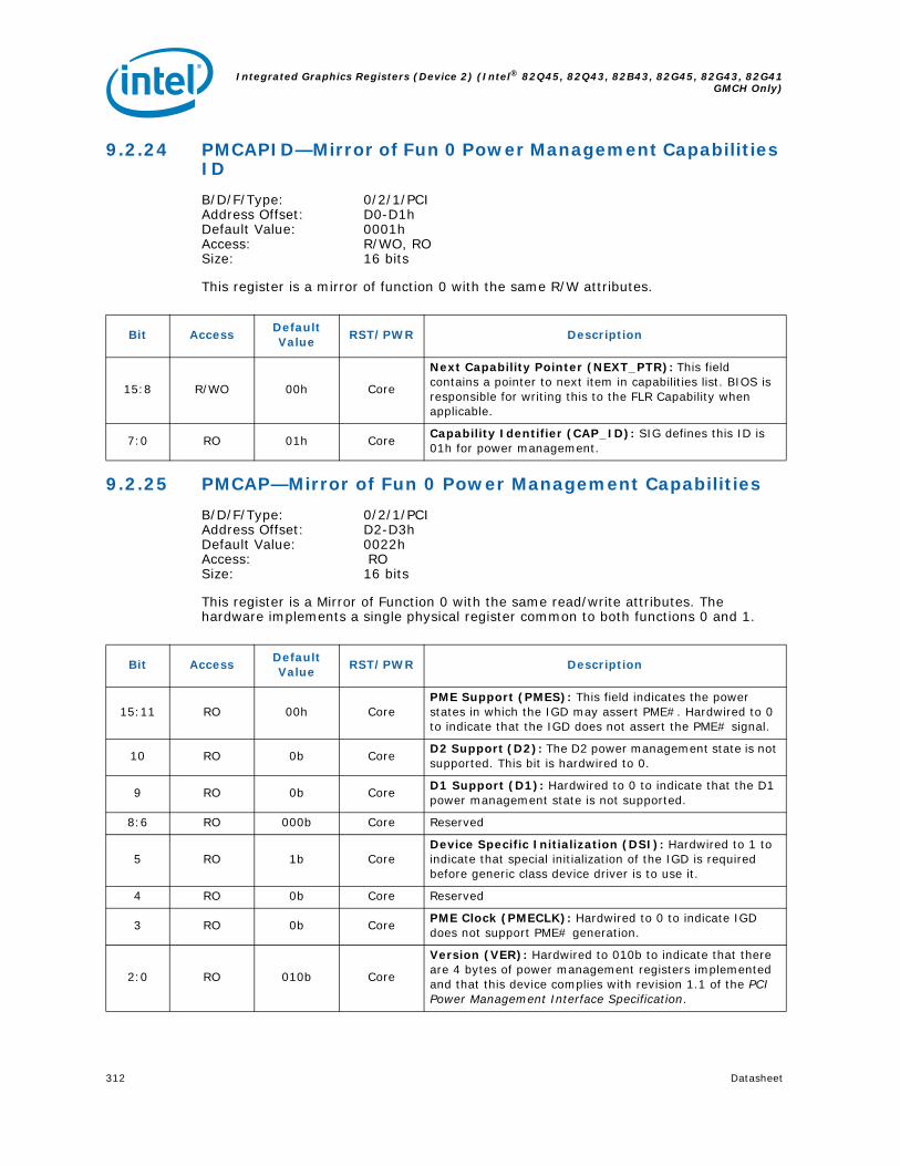
Integrated Graphics Registers (Device 2) (Intel® 82Q45, 82Q43, 82B43, 82G45, 82G43, 82G41GMCH Only)
312 Datasheet
9.2.24 PMCAPID—Mirror of Fun 0 Power Management Capabilities ID
B/D/F/Type: 0/2/1/PCIAddress Offset: D0-D1hDefault Value: 0001hAccess: R/WO, ROSize: 16 bits
This register is a mirror of function 0 with the same R/W attributes.
9.2.25 PMCAP—Mirror of Fun 0 Power Management Capabilities
B/D/F/Type: 0/2/1/PCIAddress Offset: D2-D3hDefault Value: 0022hAccess: ROSize: 16 bits
This register is a Mirror of Function 0 with the same read/write attributes. The hardware implements a single physical register common to both functions 0 and 1.
Bit AccessDefault Value
RST/PWR Description
15:8 R/WO 00h Core
Next Capability Pointer (NEXT_PTR): This field contains a pointer to next item in capabilities list. BIOS is responsible for writing this to the FLR Capability when applicable.
7:0 RO 01h CoreCapability Identifier (CAP_ID): SIG defines this ID is 01h for power management.
Bit AccessDefault Value
RST/PWR Description
15:11 RO 00h CorePME Support (PMES): This field indicates the power states in which the IGD may assert PME#. Hardwired to 0 to indicate that the IGD does not assert the PME# signal.
10 RO 0b CoreD2 Support (D2): The D2 power management state is not supported. This bit is hardwired to 0.
9 RO 0b CoreD1 Support (D1): Hardwired to 0 to indicate that the D1 power management state is not supported.
8:6 RO 000b Core Reserved
5 RO 1b CoreDevice Specific Initialization (DSI): Hardwired to 1 to indicate that special initialization of the IGD is required before generic class device driver is to use it.
4 RO 0b Core Reserved
3 RO 0b CorePME Clock (PMECLK): Hardwired to 0 to indicate IGD does not support PME# generation.
2:0 RO 010b Core
Version (VER): Hardwired to 010b to indicate that there are 4 bytes of power management registers implemented and that this device complies with revision 1.1 of the PCI Power Management Interface Specification.

Datasheet 313
Integrated Graphics Registers (Device 2) (Intel® 82Q45, 82Q43, 82B43, 82G45, 82G43, 82G41 GMCH Only)
9.2.26 PMCS—Power Management Control/Status
B/D/F/Type: 0/2/1/PCIAddress Offset: D4-D5hDefault Value: 0000hAccess: RO, R/WSize: 16 bits
9.2.27 SWSMI—Mirror of Func0 Software SMI
B/D/F/Type: 0/2/1/PCIAddress Offset: E0-E1hDefault Value: 0000hAccess: ROSize: 16 bits
Since there is the potential that DVO port legacy drivers exist that expect this register at this address, Device 2, Function 0, address E0h–E1h is reserved for this register.
§ §
Bit AccessDefault Value
RST/PWR
Description
15 RO 0b CorePME Status (PMESTS): This bit is 0 to indicate that IGD does not support PME# generation from D3 (cold).
14:13 RO 00b CoreData Scale (DSCALE): The IGD does not support data register. This bit always returns 0 when read, write operations have no effect.
12:9 RO 0h CoreData Select (DATASEL): The IGD does not support data register. This bit always returns 0 when read, write operations have no effect.
8 RO 0b CorePME Enable (PME_EN): This bit is 0 to indicate that PME# assertion from D3 (cold) is disabled.
7:2 RO 00h Core Reserved
1:0 R/W 00b FLR, Core
Power State (PWRSTAT): This field indicates the current power state of the IGD and can be used to set the IGD into a new power state. If software attempts to write an unsupported state to this field, write operation must complete normally on the bus, but the data is discarded and no state change occurs. On a transition from D3 to D0 the graphics controller is optionally reset to initial values. 00 = Default01 = D1 (Not Supported)10 = D2 (Not Supported)11 = D3
Bit AccessDefault Value
RST/PWR
Description
15:8 RO 00h Core Software Scratch Bits (SWSB):
7:1 RO 00h CoreSoftware Flag (SWF): Used to indicate caller and SMI function desired, as well as return result.
0 RO 0b CoreGMCH Software SMI Event (GSSMIE): When Set, this bit will trigger an SMI. Software must write a 0 to clear this bit.

Integrated Graphics Registers (Device 2) (Intel® 82Q45, 82Q43, 82B43, 82G45, 82G43, 82G41GMCH Only)
314 Datasheet

Datasheet 315
Intel® Manageability Engine Subsystem Registers
10 Intel® Manageability Engine Subsystem Registers
10.1 HECI Function in ME subsystem Registers
Table 17. HECI Function in ME Subsystem Register Address Map
Address Offset
Register Symbol
Register NameDefault Value
Access
0–3h ID Identifiers 2E048086h RO
4–5h CMD Command 0000h RO, R/W
6–7h STS Device Status 0010h RO
8h RID Revision IDsee
descriptionRO
9–Bh CC Class Code 0C8001h RO
Ch CLS Cache Line Size 00h RO
Dh MLT Master Latency Timer 00h RO
Eh HTYPE Header Type 80h RO
Fh BIST Built In Self Test 00h RO
10–17h HECI_MBAR HECI MMIO Base Address0000000000
000004hRO, R/W
2C–2Fh SS Sub System Identifiers 00000000h R/WO
34h CAP Capabilities Pointer 50h RO
3C–3Dh INTR Interrupt Information 0100h RO, R/W
3Eh MGNT Minimum Grant 00h RO
3F MLAT Maximum Latency 00h RO
40–43h HFS Host Firmware Status 00000000h RO
50–51h PID PCI Power Management Capability ID 8C01h RO
52–53h PC PCI Power Management Capabilities C803h RO
54–55h PMCSPCI Power Management Control And Status
0008hR/WC, RO,
R/W
8C–8Dh MIDMessage Signaled Interrupt Identifiers
0005h RO
8E–8Fh MCMessage Signaled Interrupt Message Control
0080h RO, R/W
90–93h MAMessage Signaled Interrupt Message Address
00000000h R/W, RO
94–97h MUAMessage Signaled Interrupt Upper Address (Optional)
00000000h R/W
98–99h MDMessage Signaled Interrupt Message Data
0000h R/W

Intel® Manageability Engine Subsystem Registers
316 Datasheet
10.1.1 ID— Identifiers
B/D/F/Type: 0/3/0/PCIAddress Offset: 0-3hDefault Value: 2E048086hAccess: ROSize: 32 bits
10.1.2 CMD— Command
B/D/F/Type: 0/3/0/PCIAddress Offset: 4-5hDefault Value: 0000hAccess: RO, R/WSize: 16 bits
Bit AccessDefault Value
RST/PWR Description
31:16 RO 2E04h CoreDevice ID (DID): Indicates what device number assigned by Intel.
15:0 RO 8086h CoreVendor ID (VID): 16-bit field which indicates Intel is the vendor, assigned by the PCI SIG.
Bit AccessDefault Value
RST/PWR Description
15:11 RO 00000b Core Reserved
10 R/W 0b CoreInterrupt Disable (ID): Disables this device from generating PCI line based interrupts. This bit does not have any effect on MSI operation.
9 RO 0b CoreFast Back-to-Back Enable (FBE): Not implemented, hardwired to 0.
8 RO 0b Core SERR# Enable (SEE): Not implemented, hardwired to 0.
7 RO 0b CoreWait Cycle Enable (WCC): Not implemented, hardwired to 0.
6 RO 0b CoreParity Error Response Enable (PEE): Not implemented, hardwired to 0.
5 RO 0b CoreVGA Palette Snooping Enable (VGA): Not implemented, hardwired to 0
4 RO 0b CoreMemory Write and Invalidate Enable (MWIE): Not implemented, hardwired to 0.
3 RO 0b CoreSpecial Cycle Enable (SCE): Not implemented, hardwired to 0.

Datasheet 317
Intel® Manageability Engine Subsystem Registers
10.1.3 STS— Device Status
B/D/F/Type: 0/3/0/PCIAddress Offset: 6-7hDefault Value: 0010hAccess: ROSize: 16 bits
2 R/W 0b Core
Bus Master Enable (BME): This bit controls the HECI host controller's ability to act as a system memory master for data transfers. When this bit is cleared, HECI bus master activity stops and any active DMA engines return to an idle condition. This bit is made visible to firmware through the H_PCI_CSR register, and changes to this bit may be configured by the H_PCI_CSR register to generate an ME MSI.When this bit is 0, HECI is blocked from generating MSI to the host processor.Note that this bit does not block HECI accesses to ME-UMA (i.e., writes or reads to the host and ME circular buffers through the read window and write window registers still cause ME backbone transactions to ME-UMA).
1 R/W 0b CoreMemory Space Enable (MSE): This bit controls access to the HECI host controller’s memory mapped register space.
0 RO 0b CoreI/O Space Enable (IOSE): Not implemented, hardwired to 0.
Bit AccessDefault Value
RST/PWR Description
Bit AccessDefault Value
RST/PWR Description
15 RO 0b CoreDetected Parity Error (DPE): Not implemented, hardwired to 0.
14 RO 0b CoreSignaled System Error (SSE): Not implemented, hardwired to 0.
13 RO 0b CoreReceived Master-Abort (RMA): Not implemented, hardwired to 0.
12 RO 0b CoreReceived Target Abort (RTA): Not implemented, hardwired to 0.
11 RO 0b CoreSignaled Target-Abort (STA): Not implemented, hardwired to 0.
10:9 RO 00b CoreDEVSEL# Timing (DEVT): These bits are hardwired to 00.
8 RO 0b CoreMaster Data Parity Error Detected (DPD): Not implemented, hardwired to 0.
7 RO 0b CoreFast Back-to-Back Capable (FBC): Not implemented, hardwired to 0.
6 RO 0b Core Reserved
5 RO 0b Core66 MHz Capable (C66): Not implemented, hardwired to 0.

Intel® Manageability Engine Subsystem Registers
318 Datasheet
10.1.4 RID— Revision ID
B/D/F/Type: 0/3/0/PCIAddress Offset: 8hDefault Value: see description belowAccess: ROSize: 8 bits
10.1.5 CC— Class Code
B/D/F/Type: 0/3/0/PCIAddress Offset: 9-BhDefault Value: 0C8001hAccess: ROSize: 24 bits
4 RO 1b CoreCapabilities List (CL): Indicates the presence of a capabilities list, hardwired to 1.
3 RO 0b CoreInterrupt Status (IS): Indicates the interrupt status of the device (1 = asserted).
2:0 RO 000b Core Reserved
Bit AccessDefault Value
RST/PWR Description
Bit AccessDefault Value
RST/PWR Description
7:0 ROsee
descriptionCore
Revision ID (RID): Indicates stepping of the HECI host controller. Refer to the Intel® 4 Series Chipset Family Specification Update for the value of this register.
Bit AccessDefault Value
RST/PWR Description
23:16 RO 0ch CoreBase Class Code (BCC): This field indicates the base class code of the HECI host controller device.
15:8 RO 80h CoreSub Class Code (SCC): This field indicates the sub class code of the HECI host controller device.
7:0 RO 01h CoreProgramming Interface (PI): This field indicates the programming interface of the HECI host controller device.

Datasheet 319
Intel® Manageability Engine Subsystem Registers
10.1.6 CLS— Cache Line Size
B/D/F/Type: 0/3/0/PCIAddress Offset: ChDefault Value: 00hAccess: ROSize: 8 bits
10.1.7 MLT— Master Latency Timer
B/D/F/Type: 0/3/0/PCIAddress Offset: DhDefault Value: 00hAccess: ROSize: 8 bits
10.1.8 HTYPE— Header Type
B/D/F/Type: 0/3/0/PCIAddress Offset: EhDefault Value: 80hAccess: ROSize: 8 bits
Bit AccessDefault Value
RST/PWR Description
7:0 RO 00h CoreCache Line Size (CLS): Not implemented, hardwired to 0.
Bit AccessDefault Value
RST/PWR Description
7:0 RO 00h CoreMaster Latency Timer (MLT): Not implemented, hardwired to 0.
Bit AccessDefault Value
RST/PWR Description
7 RO 1b CoreMulti-Function Device (MFD): This bit indicates the HECI host controller is part of a multi-function device.
6:0 RO 0000000b CoreHeader Layout (HL): This field indicates that the HECI host controller uses a target device layout.

Intel® Manageability Engine Subsystem Registers
320 Datasheet
10.1.9 BIST— Built In Self Test
B/D/F/Type: 0/3/0/PCIAddress Offset: FhDefault Value: 00hAccess: ROSize: 8 bits
10.1.10 HECI_MBAR— HECI MMIO Base Address
B/D/F/Type: 0/3/0/PCIAddress Offset: 10-17hDefault Value: 0000000000000004hAccess: RO, R/WSize: 64 bits
This register allocates space for the HECI memory mapped registers.
Bit AccessDefault Value
RST/PWR Description
7 RO 0b Core BIST Capable (BC): Not implemented, hardwired to 0.
6:0 RO 0000000b Core Reserved
Bit AccessDefault Value
RST/PWR Description
63:4 R/W000000000000000h
CoreBase Address (BA): Base address of register memory space.
3 RO 0b CorePrefetchable (PF): This bit indicates that this range is not pre-fetchable
2:1 RO 10b Core
Type (TP): This field indicates that this range can be mapped anywhere in 64-bit address space. Note that the (G)MCH only uses bits 35:4 of the base address field as the (G)MCH only decodes FSB address bits 35:4.
0 RO 0b CoreResource Type Indicator (RTE): Indicates a request for register memory space.

Datasheet 321
Intel® Manageability Engine Subsystem Registers
10.1.11 SS— Sub System Identifiers
B/D/F/Type: 0/3/0/PCIAddress Offset: 2C-2FhDefault Value: 00000000hAccess: R/WOSize: 32 bits
10.1.12 CAP— Capabilities Pointer
B/D/F/Type: 0/3/0/PCIAddress Offset: 34hDefault Value: 50hAccess: ROSize: 8 bits
Bit AccessDefault Value
RST/PWR Description
31:16 R/WO 0000h Core
Subsystem ID (SSID): This field indicates the sub-system identifier. This field should be programmed by BIOS during boot-up. Once written, this register becomes Read Only. This field can only be cleared by PLTRST#.
15:0 R/WO 0000h Core
Subsystem Vendor ID (SSVID): This field indicates the sub-system vendor identifier. This field should be programmed by BIOS during boot-up. Once written, this register becomes Read Only. This field can only be cleared by PLTRST#.
Bit AccessDefault Value
RST/PWR Description
7:0 RO 50h CoreCapability Pointer (CP): This field indicates the first capability pointer offset. It points to the PCI power management capability offset.

Intel® Manageability Engine Subsystem Registers
322 Datasheet
10.1.13 INTR— Interrupt Information
B/D/F/Type: 0/3/0/PCIAddress Offset: 3C-3DhDefault Value: 0100hAccess: RO, R/WSize: 16 bits
10.1.14 MGNT— Minimum Grant
B/D/F/Type: 0/3/0/PCIAddress Offset: 3EhDefault Value: 00hAccess: ROSize: 8 bits
10.1.15 MLAT— Maximum Latency
B/D/F/Type: 0/3/0/PCIAddress Offset: 3FhDefault Value: 00hAccess: ROSize: 8 bits
Bit AccessDefault Value
RST/PWR Description
15:8 RO 01h Core
Interrupt Pin (IPIN): This field indicates the interrupt pin the HECI host controller uses. The value of 01h selects INTA# interrupt pin.
NOTE: As HECI is an internal device in the (G)MCH, the INTA# pin is implemented as an INTA# message to the ICH.
7:0 R/W 00h CoreInterrupt Line (ILINE): Software written value to indicate which interrupt line (vector) the interrupt is connected to. No hardware action is taken on this register.
Bit AccessDefault Value
RST/PWR Description
7:0 RO 00h Core Grant (GNT): Not implemented, hardwired to 0.
Bit AccessDefault Value
RST/PWR Description
7:0 RO 00h Core Latency (LAT): Not implemented, hardwired to 0.

Datasheet 323
Intel® Manageability Engine Subsystem Registers
10.1.16 HFS— Host Firmware Status
B/D/F/Type: 0/3/0/PCIAddress Offset: 40-43hDefault Value: 00000000hAccess: ROSize: 32 bits
10.1.17 PID— PCI Power Management Capability ID
B/D/F/Type: 0/3/0/PCIAddress Offset: 50-51hDefault Value: 8C01hAccess: ROSize: 16 bits
Bit AccessDefault Value
RST/PWR Description
31:0 RO 00000000h Core
Firmware Status Host Access (FS_HA): This field indicates current status of the firmware for the HECI controller. This field is the host's read only access to the FS field in the ME Firmware Status AUX register.
Bit AccessDefault Value
RST/PWR Description
15:8 RO 8Ch CoreNext Capability (NEXT): This field indicates the location of the next capability item in the list. This is the Message Signaled Interrupts capability.
7:0 RO 01h CoreCap ID (CID): This field indicates that this pointer is a PCI power management.

Intel® Manageability Engine Subsystem Registers
324 Datasheet
10.1.18 PC— PCI Power Management Capabilities
B/D/F/Type: 0/3/0/PCIAddress Offset: 52-53hDefault Value: C803hAccess: ROSize: 16 bits
Bit AccessDefault Value
RST/PWR Description
15:11 RO 11001b Core
PME_Support (PSUP): This field indicates the states that can generate PME#.HECI can assert PME# from any D-state except D1 or D2 which are not supported by HECI.
10 RO 0b CoreD2_Support (D2S): The D2 state is not supported for the HECI host controller.
9 RO 0b CoreD1_Support (D1S): The D1 state is not supported for the HECI host controller.
8:6 RO 000b CoreAux_Current (AUXC): This field reports the maximum Suspend well current required when in the D3COLD state. Value of TBD is reported.
5 RO 0b CoreDevice Specific Initialization (DSI): This bit indicates whether device-specific initialization is required.
4 RO 0b Core Reserved
3 RO 0b CorePME Clock (PMEC): This bit indicates that PCI clock is not required to generate PME#.
2:0 RO 011b CoreVersion (VS): This field indicates support for Revision 1.2 of the PCI Power Management Specification.

Datasheet 325
Intel® Manageability Engine Subsystem Registers
10.1.19 PMCS— PCI Power Management Control And Status
B/D/F/Type: 0/3/0/PCIAddress Offset: 54-55hDefault Value: 0008hAccess: R/WC, RO, R/WSize: 16 bits
Bit AccessDefault Value
RST/PWR Description
15 R/WC 0b Core
PME Status (PMES): The PME Status bit in HECI space can be set to 1 by ARC FW performing a write into AUX register to set PMES.This bit is cleared by host processor writing a 1 to it.ARC cannot clear this bit.Host processor writes with value 0 have no effect on this bit.This bit is reset to 0 by MRST#.
14:9 RO 000000b Core Reserved.
8 R/W 0b Core
PME Enable (PMEE): This bit is read/write, under control of host SW. It does not directly have an effect on PME events. However, this bit is shadowed into AUX space so ARC FW can monitor it. The ARC FW is responsible for ensuring that FW does not cause the PME-S bit to transition to 1 while the PMEE bit is 0, indicating that host software had disabled PME.This bit is reset to 0 by MRST#.
7:4 RO 0000b Core Reserved
3 RO 1b Core
No_Soft_Reset (NSR): This bit indicates that when the HECI host controller is transitioning from D3hot to D0 due to power state command. It does not perform an internal reset. Configuration context is Reserved.
2 RO 0b Core Reserved
1:0 R/W 00b Core
Power State (PS): This field is used both to determine the current power state of the HECI host controller and to set a new power state. The values are:00 = D0 state11 = D3HOT stateThe D1 and D2 states are not supported for this HECI host controller. When in the D3HOT state, the HBA’s configuration space is available, but the register memory spaces are not. Additionally, interrupts are blocked. This field is visible to firmware through the H_PCI_CSR register, and changes to this field may be configured by the H_PCI_CSR register to generate an ME MSI.

Intel® Manageability Engine Subsystem Registers
326 Datasheet
10.1.20 MID— Message Signaled Interrupt Identifiers
B/D/F/Type: 0/3/0/PCIAddress Offset: 8C-8DhDefault Value: 0005hAccess: ROSize: 16 bits
10.1.21 MC— Message Signaled Interrupt Message Control
B/D/F/Type: 0/3/0/PCIAddress Offset: 8E-8FhDefault Value: 0080hAccess: RO, R/WSize: 16 bits
10.1.22 MA— Message Signaled Interrupt Message Address
B/D/F/Type: 0/3/0/PCIAddress Offset: 90-93hDefault Value: 00000000hAccess: R/W, ROSize: 32 bits
Bit AccessDefault Value
RST/PWR Description
15:8 RO 00h CoreNext Pointer (NEXT): Indicates the next item in the list. This can be other capability pointers (such as PCI-X or PCI-Express) or it can be the last item in the list.
7:0 RO 05h Core Capability ID (CID): Capabilities ID indicates MSI.
Bit AccessDefault Value
RST/PWR Description
15:8 RO 00h Core Reserved
7 RO 1b Core64 Bit Address Capable (C64): Specifies whether capable of generating 64-bit messages.
6:4 RO 000b CoreMultiple Message Enable (MME): Not implemented, hardwired to 0.
3:1 RO 000b CoreMultiple Message Capable (MMC): Not implemented, hardwired to 0.
0 R/W 0b CoreMSI Enable (MSIE): If set, MSI is enabled and traditional interrupt pins are not used to generate interrupts.
Bit AccessDefault Value
RST/PWR Description
31:2 R/W 00000000h CoreAddress (ADDR): Lower 32 bits of the system specified message address, always DWord aligned.
1:0 RO 00b Core Reserved

Datasheet 327
Intel® Manageability Engine Subsystem Registers
10.1.23 MUA— Message Signaled Interrupt Upper Address (Optional)
B/D/F/Type: 0/3/0/PCIAddress Offset: 94-97hDefault Value: 00000000hAccess: R/WSize: 32 bits
10.1.24 MD— Message Signaled Interrupt Message Data
B/D/F/Type: 0/3/0/PCIAddress Offset: 98-99hDefault Value: 0000hAccess: R/WSize: 16 bits
Bit AccessDefault Value
RST/PWR Description
31:0 R/W 00000000h CoreUpper Address (UADDR): Upper 32 bits of the system specified message address. This register is optional and only implemented if MC.C64=1.
Bit AccessDefault Value
RST/PWR Description
15:0 R/W 0000h Core
Data (Data): This 16-bit field is programmed by system software if MSI is enabled. Its content is driven onto the FSB during the data phase of the MSI memory write transaction.

Intel® Manageability Engine Subsystem Registers
328 Datasheet
10.2 Second HECI Function in ME Subsystem Registers
Table 18. Second HECI Function in ME Subsystem Register Address Map
Address Offset
Register Symbol
Register NameDefault Value
Access
0–3h ID Identifiers 2E058086h RO
4–5h CMD Command 0000h RO, R/W
6–7h STS Device Status 0010h RO
8h RID Revision IDsee register description
RO
9–Bh CC Class Code 0C8001h RO
Ch CLS Cache Line Size 00h RO
Dh MLT Master Latency Timer 00h RO
Eh HTYPE Header Type 80h RO
10–17h HECI_MBAR HECI MMIO Base Address0000000000
000004hR/W, RO
2C–2Fh SS Sub System Identifiers 00000000h R/WO
34h CAP Capabilities Pointer 50h RO
3C–3Dh INTR Interrupt Information 0100h R/W, RO
3Eh MGNT Minimum Grant 00h RO
3Fh MLAT Maximum Latency 00h RO
40–43h HFS Host Firmware Status 00000000h RO
50–51h PID PCI Power Management Capability ID 8C01h RO
52–53h PC PCI Power Management Capabilities C803h RO
54–55h PMCSPCI Power Management Control And Status
0008hR/W, RO, R/
WC
8C–h8D MID Message Signaled Interrupt Identifiers 0005h RO
8E–8Fh MCMessage Signaled Interrupt Message Control
0080h R/W, RO
90–93h MAMessage Signaled Interrupt Message Address
00000000h R/W, RO
94–97h MUAMessage Signaled Interrupt Upper Address (Optional)
00000000h R/W
98–99h MDMessage Signaled Interrupt Message Data
0000h R/W
A0h HIDM HECI Interrupt Delivery Mode 00h R/W

Datasheet 329
Intel® Manageability Engine Subsystem Registers
10.2.1 ID— Identifiers
B/D/F/Type: 0/3/1/PCIAddress Offset: 0-3hDefault Value: 2E058086hAccess: ROSize: 32 bits
10.2.2 CMD— Command
B/D/F/Type: 0/3/1/PCIAddress Offset: 4-5hDefault Value: 0000hAccess: RO, R/WSize: 16 bits
Bit AccessDefault Value
RST/PWR Description
31:16 RO 2E05h CoreDevice ID (DID): Indicates what device number assigned by Intel.
15:0 RO 8086h CoreVendor ID (VID): 16-bit field which indicates Intel is the vendor, assigned by the PCI SIG.
Bit AccessDefault Value
RST/PWR Description
15:11 RO 00000b Core Reserved
10 R/W 0b CoreInterrupt Disable (ID): Disables this device from generating PCI line based interrupts. This bit does not have any effect on MSI operation.
9 RO 0b CoreFast Back-to-Back Enable (FBE): Not implemented, hardwired to 0.
8 RO 0b Core SERR# Enable (SEE): Not implemented, hardwired to 0.
7 RO 0b CoreWait Cycle Enable (WCC): Not implemented, hardwired to 0.
6 RO 0b CoreParity Error Response Enable (PEE): Not implemented, hardwired to 0.
5 RO 0b CoreVGA Palette Snooping Enable (VGA): Not implemented, hardwired to 0
4 RO 0b CoreMemory Write and Invalidate Enable (MWIE): Not implemented, hardwired to 0.
3 RO 0b CoreSpecial Cycle Enable (SCE): Not implemented, hardwired to 0.

Intel® Manageability Engine Subsystem Registers
330 Datasheet
10.2.3 STS— Device Status
B/D/F/Type: 0/3/1/PCIAddress Offset: 6-7hDefault Value: 0010hAccess: ROSize: 16 bits
2 R/W 0b Core
Bus Master Enable (BME): This bit controls the HECI host controller's ability to act as a system memory master for data transfers. When this bit is cleared, HECI bus master activity stops and any active DMA engines return to an idle condition. This bit is made visible to firmware through the H_PCI_CSR register, and changes to this bit may be configured by the H_PCI_CSR register to generate an ME MSI.When this bit is 0, HECI is blocked from generating MSI to the host processor.Note that this bit does not block HECI accesses to ME-UMA (i.e., writes or reads to the host and ME circular buffers through the read window and write window registers still cause ME backbone transactions to ME-UMA).
1 R/W 0b CoreMemory Space Enable (MSE): This bit controls access to the HECI host controller’s memory mapped register space.
0 RO 0b CoreI/O Space Enable (IOSE): Not implemented, hardwired to 0.
Bit AccessDefault Value
RST/PWR Description
Bit AccessDefault Value
RST/PWR Description
15 RO 0b CoreDetected Parity Error (DPE): Not implemented, hardwired to 0.
14 RO 0b CoreSignaled System Error (SSE): Not implemented, hardwired to 0.
13 RO 0b CoreReceived Master-Abort (RMA): Not implemented, hardwired to 0.
12 RO 0b CoreReceived Target Abort (RTA): Not implemented, hardwired to 0.
11 RO 0b CoreSignaled Target-Abort (STA): Not implemented, hardwired to 0.
10:9 RO 00b CoreDEVSEL# Timing (DEVT): These bits are hardwired to 00.
8 RO 0b CoreMaster Data Parity Error Detected (DPD): Not implemented, hardwired to 0.
7 RO 0b CoreFast Back-to-Back Capable (FBC): Not implemented, hardwired to 0.
6 RO 0b Core Reserved
5 RO 0b Core66 MHz Capable (C66): Not implemented, hardwired to 0.

Datasheet 331
Intel® Manageability Engine Subsystem Registers
10.2.4 RID—Revision ID
B/D/F/Type: 0/3/1/PCIAddress Offset: 8hDefault Value: 02hsee description belowAccess: ROSize: 8 bits
10.2.5 CC— Class Code
B/D/F/Type: 0/3/1/PCIAddress Offset: 9-BhDefault Value: 0C8001hAccess: ROSize: 24 bits
4 RO 1b CoreCapabilities List (CL): Indicates the presence of a capabilities list, hardwired to 1.
3 RO 0b CoreInterrupt Status (IS): Indicates the interrupt status of the device (1 = asserted).
2:0 RO 000b Core Reserved
Bit AccessDefault Value
RST/PWR Description
Bit AccessDefault Value
RST/PWR Description
7:0 ROsee
descriptionCore
Revision ID (RID): This field indicates stepping of the HECI host controller. Refer to the Intel® 4 Series Chipset Family Specification Update for the value of this register.
Bit AccessDefault Value
RST/PWR Description
23:16 RO 0ch CoreBase Class Code (BCC): This field indicates the base class code of the HECI host controller device.
15:8 RO 80h CoreSub Class Code (SCC): This field indicates the sub class code of the HECI host controller device.
7:0 RO 01h CoreProgramming Interface (PI): This field indicates the programming interface of the HECI host controller device.

Intel® Manageability Engine Subsystem Registers
332 Datasheet
10.2.6 CLS— Cache Line Size
B/D/F/Type: 0/3/1/PCIAddress Offset: ChDefault Value: 00hAccess: ROSize: 8 bits
10.2.7 MLT— Master Latency Timer
B/D/F/Type: 0/3/1/PCIAddress Offset: DhDefault Value: 00hAccess: ROSize: 8 bits
10.2.8 HTYPE— Header Type
B/D/F/Type: 0/3/1/PCIAddress Offset: EhDefault Value: 80hAccess: ROSize: 8 bits
Bit AccessDefault Value
RST/PWR Description
7:0 RO 00h CoreCache Line Size (CLS): Not implemented, hardwired to 0.
Bit AccessDefault Value
RST/PWR Description
7:0 RO 00h CoreMaster Latency Timer (MLT): Not implemented, hardwired to 0.
Bit AccessDefault Value
RST/PWR Description
7 RO 1b CoreMulti-Function Device (MFD): This bit indicates the HECI host controller is part of a multi-function device.
6:0 RO 0000000b CoreHeader Layout (HL): This field indicates that the HECI host controller uses a target device layout.

Datasheet 333
Intel® Manageability Engine Subsystem Registers
10.2.9 HECI_MBAR— HECI MMIO Base Address
B/D/F/Type: 0/3/1/PCIAddress Offset: 10-17hDefault Value: 0000000000000004hAccess: R/W, ROSize: 64 bits
This register allocates space for the HECI memory mapped registers.
10.2.10 SS— Sub System Identifiers
B/D/F/Type: 0/3/1/PCIAddress Offset: 2C-2FhDefault Value: 00000000hAccess: R/WOSize: 32 bits
Bit AccessDefault Value
RST/PWR Description
63:4 R/W000000000000000h
CoreBase Address (BA): Base address of register memory space.
3 RO 0b CorePrefetchable (PF): This bit indicates that this range is not pre-fetchable
2:1 RO 10b CoreType (TP): This field indicates that this range can be mapped anywhere in 32-bit address space
0 RO 0b CoreResource Type Indicator (RTE): This bit indicates a request for register memory space.
Bit AccessDefault Value
RST/PWR Description
31:16 R/WO 0000h Core
Subsystem ID (SSID): This field indicates the sub-system identifier. This field should be programmed by BIOS during boot-up. Once written, this register becomes Read Only. This field can only be cleared by PLTRST#.
15:0 R/WO 0000h Core
Subsystem Vendor ID (SSVID): This field indicates the sub-system vendor identifier. This field should be programmed by BIOS during boot-up. Once written, this register becomes Read Only. This field can only be cleared by PLTRST#.

Intel® Manageability Engine Subsystem Registers
334 Datasheet
10.2.11 CAP— Capabilities Pointer
B/D/F/Type: 0/3/1/PCIAddress Offset: 34hDefault Value: 50hAccess: ROSize: 8 bits
10.2.12 INTR— Interrupt Information
B/D/F/Type: 0/3/1/PCIAddress Offset: 3C-3DhDefault Value: 0100hAccess: R/W, ROSize: 16 bits
10.2.13 MGNT— Minimum Grant
B/D/F/Type: 0/3/1/PCIAddress Offset: 3EhDefault Value: 00hAccess: ROSize: 8 bits
Bit AccessDefault Value
RST/PWR Description
7:0 RO 50h CoreCapability Pointer (CP): This field indicates the first capability pointer offset. It points to the PCI power management capability offset.
Bit AccessDefault Value
RST/PWR Description
15:8 RO 01h Core
Interrupt Pin (IPIN): This field indicates the interrupt pin the HECI host controller uses. The value of 01h selects INTA# interrupt pin.
NOTE: As HECI is an internal device in the (G)MCH, the INTA# pin is implemented as an INTA# message to the ICH.
7:0 R/W 00h CoreInterrupt Line (ILINE): Software written value to indicate which interrupt line (vector) the interrupt is connected to. No hardware action is taken on this register.
Bit AccessDefault Value
RST/PWR Description
7:0 RO 00h Core Grant (GNT): Not implemented, hardwired to 0.

Datasheet 335
Intel® Manageability Engine Subsystem Registers
10.2.14 MLAT— Maximum Latency
B/D/F/Type: 0/3/1/PCIAddress Offset: 3FhDefault Value: 00hAccess: ROSize: 8 bits
10.2.15 HFS— Host Firmware Status
B/D/F/Type: 0/3/1/PCIAddress Offset: 40-43hDefault Value: 00000000hAccess: ROSize: 32 bits
10.2.16 PID— PCI Power Management Capability ID
B/D/F/Type: 0/3/1/PCIAddress Offset: 50-51hDefault Value: 8C01hAccess: ROSize: 16 bits
Bit AccessDefault Value
RST/PWR Description
7:0 RO 00h Core Latency (LAT): Not implemented, hardwired to 0.
Bit AccessDefault Value
RST/PWR Description
31:0 RO 00000000h Core
Firmware Status Host Access (FS_HA): This field indicates current status of the firmware for the HECI controller. This field is the host's read only access to the FS field in the ME Firmware Status AUX register.
Bit AccessDefault Value
RST/PWR Description
15:8 RO 8Ch CoreNext Capability (NEXT): This field indicates the location of the next capability item in the list. This is the Message Signaled Interrupts capability.
7:0 RO 01h CoreCap ID (CID): This field indicates that this pointer is a PCI power management.

Intel® Manageability Engine Subsystem Registers
336 Datasheet
10.2.17 PC— PCI Power Management Capabilities
B/D/F/Type: 0/3/1/PCIAddress Offset: 52-53hDefault Value: C803hAccess: ROSize: 16 bits
Bit AccessDefault Value
RST/PWR Description
15:11 RO 11001b Core
PME_Support (PSUP): This field indicates the states that can generate PME#.HECI can assert PME# from any D-state except D1 or D2 which are not supported by HECI.
10 RO 0b CoreD2_Support (D2S): The D2 state is not supported for the HECI host controller.
9 RO 0b CoreD1_Support (D1S): The D1 state is not supported for the HECI host controller.
8:6 RO 000b CoreAux_Current (AUXC): This field reports the maximum Suspend well current required when in the D3COLD state.
5 RO 0b CoreDevice Specific Initialization (DSI): This bit indicates whether device-specific initialization is required.
4 RO 0b Core Reserved
3 RO 0b CorePME Clock (PMEC): This bit indicates that PCI clock is not required to generate PME#.
2:0 RO 011b CoreVersion (VS): Indicates support for the PCI Power Management Specification, Revision 1.2.

Datasheet 337
Intel® Manageability Engine Subsystem Registers
10.2.18 PMCS— PCI Power Management Control And Status
B/D/F/Type: 0/3/1/PCIAddress Offset: 54-55hDefault Value: 0008hAccess: R/W, RO, R/WCSize: 16 bits
Bit AccessDefault Value
RST/PWR Description
15 R/WC 0b Core
PME Status (PMES): The PME Status bit in HECI space can be set to 1 by ARC FW performing a write into AUX register to set PMES.This bit is cleared by host processor writing a 1 to it.ARC cannot clear this bit.Host processor writes with value 0 have no effect on this bit.This bit is reset to 0 by MRST#.
14:9 RO 000000b Core Reserved.
8 R/W 0b Core
PME Enable (PMEE): This bit is read/write, under control of host software. It does not directly have an effect on PME events. However, this bit is shadowed into AUX space so ARC FW can monitor it. The ARC FW is responsible for ensuring that FW does not cause the PME-S bit to transition to 1 while the PMEE bit is 0, indicating that host SW had disabled PME.This bit is reset to 0 by MRST#.
7:4 RO 0000b Core Reserved
3 RO 1b Core
No_Soft_Reset (NSR): This bit indicates that when the HECI host controller is transitioning from D3hot to D0 due to power state command, it does not perform and internal reset. Configuration context is Reserved.
2 RO 0b Core Reserved
1:0 R/W 00b Core
Power State (PS): This field is used both to determine the current power state of the HECI host controller and to set a new power state. The values are:00 = D0 state11 = D3HOT stateThe D1 and D2 states are not supported for this HECI host controller. When in the D3HOT state, the HBA’s configuration space is available, but the register memory spaces are not. Additionally, interrupts are blocked. This field is visible to firmware through the H_PCI_CSR register, and changes to this field may be configured by the H_PCI_CSR register to generate an ME MSI.

Intel® Manageability Engine Subsystem Registers
338 Datasheet
10.2.19 MID— Message Signaled Interrupt Identifiers
B/D/F/Type: 0/3/1/PCIAddress Offset: 8C-8DhDefault Value: 0005hAccess: ROSize: 16 bits
10.2.20 MC— Message Signaled Interrupt Message Control
B/D/F/Type: 0/3/1/PCIAddress Offset: 8E-8FhDefault Value: 0080hAccess: R/W, ROSize: 16 bits
10.2.21 MA— Message Signaled Interrupt Message Address
B/D/F/Type: 0/3/1/PCIAddress Offset: 90-93hDefault Value: 00000000hAccess: R/W, ROSize: 32 bits
Bit AccessDefault Value
RST/PWR Description
15:8 RO 00h CoreNext Pointer (NEXT): This field indicates the next item in the list. This can be other capability pointers (such as PCI-X or PCI-Express) or it can be the last item in the list.
7:0 RO 05h Core Capability ID (CID): Capabilities ID indicates MSI.
Bit AccessDefault Value
RST/PWR Description
15:8 RO 00h Core Reserved
7 RO 1b Core64 Bit Address Capable (C64): Specifies whether capable of generating 64-bit messages.
6:4 RO 000b CoreMultiple Message Enable (MME): Not implemented, hardwired to 0.
3:1 RO 000b CoreMultiple Message Capable (MMC): Not implemented, hardwired to 0.
0 R/W 0b CoreMSI Enable (MSIE): If set, MSI is enabled and traditional interrupt pins are not used to generate interrupts.
Bit AccessDefault Value
RST/PWR Description
31:2 R/W 00000000h CoreAddress (ADDR): Lower 32 bits of the system specified message address, always DW aligned.
1:0 RO 00b Core Reserved

Datasheet 339
Intel® Manageability Engine Subsystem Registers
10.2.22 MUA— Message Signaled Interrupt Upper Address (Optional)
B/D/F/Type: 0/3/1/PCIAddress Offset: 94-97hDefault Value: 00000000hAccess: R/WSize: 32 bits
10.2.23 MD— Message Signaled Interrupt Message Data
B/D/F/Type: 0/3/1/PCIAddress Offset: 98-99hDefault Value: 0000hAccess: R/WSize: 16 bits
10.2.24 HIDM—HECI Interrupt Delivery Mode
B/D/F/Type: 0/3/1/PCIAddress Offset: A0hDefault Value: 00hAccess: R/WSize: 8 bitsBIOS Optimal Default 00h
This register is used to select interrupt delivery mechanism for HECI to Host processor interrupts.
Bit AccessDefault Value
RST/PWR Description
31:0 R/W 00000000h CoreUpper Address (UADDR): Upper 32 bits of the system specified message address. This register is optional and only implemented if MC.C64=1.
Bit AccessDefault Value
RST/PWR Description
15:0 R/W 0000h Core
Data (Data): This 16-bit field is programmed by system software if MSI is enabled. Its content is driven onto the FSB during the data phase of the MSI memory write transaction.
Bit AccessDefault Value
RST/PWR Description
7:2 RO 0h Reserved
1:0 R/W 00b Core
HECI Interrupt Delivery Mode (HIDM): These bits control what type of interrupt the HECI will send when ARC writes to set the M_IG bit in AUX space. They are interpreted as follows:00 = Generate Legacy or MSI interrupt01 = Generate SCI10 = Generate SMI

Intel® Manageability Engine Subsystem Registers
340 Datasheet
10.3 HECI PCI MMIO Space Registers
10.3.1 H_CB_WW— Host Circular Buffer Write Window
B/D/F/Type: 0/3/0/MMIOAddress Offset: 0-3hDefault Value: 00000000hAccess: WSize: 32 bits
This register is for host to write into its Circular Buffer (H_CB). The host’s circular buffer is located at the ME subsystem address specified in the Host CB Base Address register.
Table 19. HECI PCI MMIO space Register Address Map
Address Offset
Register Symbol
Register NameDefault Value
Access
0–3h H_CB_WW Host Circular Buffer Write Window 00000000h W
4–7h H_CSR Host Control Status 02000000hRO, R/W,
R/WC
8–Bh ME_CB_RW ME Circular Buffer Read Window FFFFFFFFh RO
C–Fh ME_CSR_HA ME Control Status Host Access 02000000h RO
Bit AccessDefault Value
RST/PWR Description
31:0 W 00000000h Core
Host Circular Buffer Write Window Field (H_CB_WWF): This bit field is for host to write into its circular buffer. The host's circular buffer is located at the ME subsystem address specified in the Host CB Base Address register. This field is write only, reads will return arbitrary data. Writes to this register will increment the H_CBWP as long as ME_RDY is 1. When ME_RDY is 0, writes to this register have no effect and are not delivered to the H_CB, nor is H_CBWP incremented.

Datasheet 341
Intel® Manageability Engine Subsystem Registers
10.3.2 H_CSR— Host Control Status
B/D/F/Type: 0/3/0/MMIOAddress Offset: 4-7hDefault Value: 02000000hAccess: RO, R/W, R/WCSize: 32 bits
This register reports status information about the host circular buffer (H_CB) and allows host software to control interrupt generation. Note to software: reserved bits in this register must be set to 0 whenever this register is written.
Bit AccessDefault Value
RST/PWR Description
31:24 RO 02h Core
Host Circular Buffer Depth (H_CBD): This field indicates the maximum number of 32 bit entries available in the host circular buffer (H_CB). Host software uses this field along with the H_CBRP and H_CBWP fields to calculate the number of valid entries in the H_CB to read or number of entries available for write. This field is a read only version of H_CBD_MERWA field which is programmed by the ME firmware during ME initialization.Programmer's note: This field is implemented with a "1-hot" scheme. Only one bit will be set to a 1 at a time. Each bit position represents the value n of a buffer depth of (2^n). For example, when bit 1 is 1, the buffer depth is 2; when bit 2 is 1, the buffer depth is 4, etc. The allowed buffer depth values are 2, 4, 8, 16, 32, 64 and 128.This field is reset by MERST#.
23:16 RO 00h Core
Host CB Write Pointer (H_CBWP): This field points to next location in the H_CB for host to write the data. Software uses this field along with H_CBRP and H_CBD fields to calculate the number of valid entries in the H_CB to read or number of entries available for write.
15:8 RO 00h Core
Host CB Read Pointer (H_CBRP): This field points to next location in the H_CB where a valid data is available for embedded controller to read. Software uses this field along with H_CBWR and H_CBD fields to calculate the number of valid entries in the host CB to read or number of entries available for write.
7:5 RO 000b Core Reserved
4 R/W 0b Core
Host Reset (H_RST): Setting this bit to 1 will initiate a HECI reset sequence to get the circular buffers into a known good state for host and ME communication. When this bit transitions from 0-to-1, hardware will clear the H_RDY and ME_RDY bits.
3 R/W 0b CoreHost Ready (H_RDY): This bit indicates that the host is ready to process messages.

Intel® Manageability Engine Subsystem Registers
342 Datasheet
10.3.3 ME_CB_RW— ME Circular Buffer Read Window
B/D/F/Type: 0/3/0/MMIOAddress Offset: 8-BhDefault Value: FFFFFFFFhAccess: ROSize: 32 bits
This register is for host to read from the ME Circular Buffer (ME_CB). The ME's circular buffer is located at the ME subsystem address specified in the ME CB Base Address register.
2 R/W 0b Core
Host Interrupt Generate (H_IG): Once message(s) are written into its CB, the host sets this bit to 1 for the hardware to set the ME_IS bit in the ME_CSR and to generate an interrupt message to ME. Hardware will send the interrupt message to ME only if the ME_IE is enabled. Hardware then clears this bit to 0.
1 R/WC 0b Core
Host Interrupt Status (H_IS): Hardware sets this bit to 1 when ME_IG bit is set to 1. Host clears this bit to 0 by writing a 1 to this bit position. H_IE has no effect on this bit.
0 R/W 0b CoreHost Interrupt Enable (H_IE): Host sets this bit to 1 to enable the host interrupt (INTR# or MSI) to be asserted when H_IS is set to 1.
Bit AccessDefault Value
RST/PWR Description
Bit AccessDefault Value
RST/PWR Description
31:0 RO FFFFFFFFh Core
ME Circular Buffer Read Window Field (ME_CB_RWF): This bit field is for host to read from the ME Circular Buffer. The ME's circular buffer is located at the ME subsystem address specified in the ME CB Base Address register. This field is read only, writes have no effect. Reads to this register will increment the ME_CBRP as long as ME_RDY is 1. When ME_RDY is 0, reads to this register have no effect, all 1s are returned, and ME_CBRP is not incremented.

Datasheet 343
Intel® Manageability Engine Subsystem Registers
10.3.4 ME_CSR_HA— ME Control Status Host Access
B/D/F/Type: 0/3/0/MMIOAddress Offset: C-FhDefault Value: 02000000hAccess: ROSize: 32 bits
This register allows host software to read the ME Control Status register (ME_CSR). This register is reset by MERST#.
Bit AccessDefault Value
RST/PWR Description
31:24 RO 02h CoreME Circular Buffer Depth Host Read Access (ME_CBD_HRA): Host read only access to ME_CBD.
23:16 RO 00h CoreME CB Write Pointer Host Read Access (ME_CBWP_HRA): Host read only access to ME_CBWP.
15:8 RO 00h CoreME CB Read Pointer Host Read Access (ME_CBRP_HRA): Host read only access to ME_CBRP.
7:5 RO 000b Core Reserved
4 RO 0b CoreME Reset Host Read Access (ME_RST_HRA): Host read access to ME_RST.
3 RO 0b CoreME Ready Host Read Access (ME_RDY_HRA): Host read access to ME_RDY.
2 RO 0b CoreME Interrupt Generate Host Read Access (ME_IG_HRA): Host read only access to ME_IG.
1 RO 0b CoreME Interrupt Status Host Read Access (ME_IS_HRA): Host read only access to ME_IS.
0 RO 0b CoreME Interrupt Enable Host Read Access (ME_IE_HRA): Host read only access to ME_IE.

Intel® Manageability Engine Subsystem Registers
344 Datasheet
10.4 Second HECI Function MMIO Space Registers
10.4.1 H_CB_WW— Host Circular Buffer Write Window
B/D/F/Type: 0/3/1/MMIOAddress Offset: 0-3hDefault Value: 00000000hAccess: WSize: 32 bits
This register is for host to write into its Circular Buffer (H_CB). The host’s circular buffer is located at the ME subsystem address specified in the Host CB Base Address register.
Table 20. Second HECI function MMIO Space Register Address Map
Address Offset
Register Symbol
Register NameDefault Value
Access
0–3h H_CB_WW Host Circular Buffer Write Window 00000000h W
4–7h H_CSR Host Control Status 02000000hRO, R/W,
R/WC
8–Bh ME_CB_RW ME Circular Buffer Read Window FFFFFFFFh RO
C–Fh ME_CSR_HA ME Control Status Host Access 02000000h RO
Bit AccessDefault Value
RST/PWR Description
31:0 W 00000000h Core
Host Circular Buffer Write Window Field (H_CB_WWF): This bit field is for host to write into its circular buffer. The host's circular buffer is located at the ME subsystem address specified in the Host CB Base Address register. This field is write only, reads will return arbitrary data. Writes to this register will increment the H_CBWP as long as ME_RDY is 1. When ME_RDY is 0, writes to this register have no effect and are not delivered to the H_CB, nor is H_CBWP incremented.

Datasheet 345
Intel® Manageability Engine Subsystem Registers
10.4.2 H_CSR— Host Control Status
B/D/F/Type: 0/3/1/MMIOAddress Offset: 4-7hDefault Value: 02000000hAccess: RO, R/W, R/WCSize: 32 bits
This register reports status information about the host circular buffer (H_CB) and allows host software to control interrupt generation.
Note: Reserved bits in this register must be set to 0 whenever this register is written.
Bit AccessDefault Value
RST/PWR Description
31:24 RO 02h Core
Host Circular Buffer Depth (H_CBD): This field indicates the maximum number of 32 bit entries available in the host circular buffer (H_CB). Host software uses this field along with the H_CBRP and H_CBWP fields to calculate the number of valid entries in the H_CB to read or number of entries available for write. This field is a read only version of H_CBD_MERWA field which is programmed by the ME firmware during ME initialization.Programer's note: This field is implemented with a "1-hot" scheme. Only one bit will be set to a 1 at a time. Each bit position represents the value n of a buffer depth of (2^n). For example, when bit 0 is 1, the buffer depth is 1; when bit 1 is 1, the buffer depth is 2, etc. The allowed buffer depth values are 2, 4, 8, 16, 32, 64 and 128.This field is reset by MERST#.
23:16 RO 00h Core
Host CB Write Pointer (H_CBWP): This field points to next location in the H_CB for host to write the data. Software uses this field along with H_CBRP and H_CBD fields to calculate the number of valid entries in the H_CB to read or number of entries available for write.
15:8 RO 00h Core
Host CB Read Pointer (H_CBRP): This field points to next location in the H_CB where a valid data is available for embedded controller to read. Software uses this field along with H_CBWR and H_CBD fields to calculate the number of valid entries in the host CB to read or number of entries available for write.
7:5 RO 000b Core Reserved
4 R/W 0b Core
Host Reset (H_RST): Setting this bit to 1 will initiate a HECI reset sequence to get the circular buffers into a known good state for host and ME communication. When this bit transitions from 0 to 1, hardware will clear the H_RDY and ME_RDY bits.
3 R/W 0b CoreHost Ready (H_RDY): This bit indicates that the host is ready to process messages.

Intel® Manageability Engine Subsystem Registers
346 Datasheet
10.4.3 ME_CB_RW— ME Circular Buffer Read Window
B/D/F/Type: 0/3/1/MMIOAddress Offset: 8-BhDefault Value: FFFFFFFFhAccess: ROSize: 32 bits
This register is for host to read from the ME Circular Buffer (ME_CB). The ME's circular buffer is located at the ME subsystem address specified in the ME CB Base Address register.
2 R/W 0b Core
Host Interrupt Generate (H_IG): Once message(s) are written into its CB, the host sets this bit to 1 for the hardware to set the ME_IS bit in the ME_CSR and to generate an interrupt message to ME. Hardware will send the interrupt message to ME only if the ME_IE is enabled. Hardware then clears this bit to 0.
1 R/WC 0b Core
Host Interrupt Status (H_IS): Hardware sets this bit to 1 when ME_IG bit is set to 1. Host clears this bit to 0 by writing a 1 to this bit position. H_IE has no effect on this bit.
0 R/W 0b CoreHost Interrupt Enable (H_IE): The Host sets this bit to 1 to enable the host interrupt (INTR# or MSI) to be asserted when H_IS is set to 1.
Bit AccessDefault Value
RST/PWR Description
Bit AccessDefault Value
RST/PWR Description
31:0 RO FFFFFFFFh Core
ME Circular Buffer Read Window Field (ME_CB_RWF): This bit field is for host to read from the ME Circular Buffer. The ME's circular buffer is located at the ME subsystem address specified in the ME CB Base Address register. This field is read only, writes have no effect. Reads to this register will increment the ME_CBRP as long as ME_RDY is 1. When ME_RDY is 0, reads to this register have no effect, all 1s are returned, and ME_CBRP is not incremented.

Datasheet 347
Intel® Manageability Engine Subsystem Registers
10.4.4 ME_CSR_HA— ME Control Status Host Access
B/D/F/Type: 0/3/1/MMIOAddress Offset: C-FhDefault Value: 02000000hAccess: ROSize: 32 bits
This register allows host software to read the ME Control Status register (ME_CSR). This register is reset by MERST#.
Bit AccessDefault Value
RST/PWR Description
31:24 RO 02h CoreME Circular Buffer Depth Host Read Access (ME_CBD_HRA): Host read only access to ME_CBD.
23:16 RO 00h CoreME CB Write Pointer Host Read Access (ME_CBWP_HRA): Host read only access to ME_CBWP.
15:8 RO 00h CoreME CB Read Pointer Host Read Access (ME_CBRP_HRA): Host read only access to ME_CBRP.
7:5 RO 000b Core Reserved
4 RO 0b CoreME Reset Host Read Access (ME_RST_HRA): Host read access to ME_RST.
3 RO 0b CoreME Ready Host Read Access (ME_RDY_HRA): Host read access to ME_RDY.
2 RO 0b CoreME Interrupt Generate Host Read Access (ME_IG_HRA): Host read only access to ME_IG.
1 RO 0b CoreME Interrupt Status Host Read Access (ME_IS_HRA): Host read only access to ME_IS.
0 RO 0b CoreME Interrupt Enable Host Read Access (ME_IE_HRA): Host read only access to ME_IE.

Intel® Manageability Engine Subsystem Registers
348 Datasheet
10.5 IDE Function for Remote Boot and Installations PT IDER Registers
Table 21. IDE Function for remote boot and Installations PT IDER Register Address Map
Address Offset
Register Symbol
Register NameDefault Value
Access
0–3h ID Identification 2E068086h RO
4–5h CMD Command Register 0000h RO, R/W
6–7h STS Device Status 00B0h RO
8h RID Revision IDsee register description
RO
9–Bh CC Class Codes 010185h RO
Ch CLS Cache Line Size 00h RO
Dh MLT Master Latency Timer 00h RO
10–13h PCMDBA Primary Command Block IO Bar 00000001h RO, R/W
14–17h PCTLBA Primary Control Block Base Address 00000001h RO, R/W
18–1Bh SCMDBA Secondary Command Block Base Address 00000001h RO, R/W
1C–1Fh SCTLBA Secondary Control Block base Address 00000001h RO, R/W
20–23h LBAR Legacy Bus Master Base Address 00000001h RO, R/W
2C–2Fh SS Sub System Identifiers 00008086h R/WO
30–33h EROM Expansion ROM Base Address 00000000h RO
34h CAP Capabilities Pointer C8h RO
3C–3Dh INTR Interrupt Information 0300h R/W, RO
3Eh MGNT Minimum Grant 00h RO
3Fh MLAT Maximum Latency 00h RO
C8–C9h PID PCI Power Management Capability ID D001h RO
CA–CBh PC PCI Power Management Capabilities 0023h RO
CC–CFh PMCS PCI Power Management Control and Status 00000000hRO, R/W,
RO/V
D0–D1h MID Message Signaled Interrupt Capability ID 0005h RO
D2–D3h MCMessage Signaled Interrupt Message Control
0080h RO, R/W
D4–D7h MAMessage Signaled Interrupt Message Address
00000000h R/W, RO
D8–DBh MAUMessage Signaled Interrupt Message Upper Address
00000000h RO, R/W
DC–DDh MD Message Signaled Interrupt Message Data 0000h R/W

Datasheet 349
Intel® Manageability Engine Subsystem Registers
10.5.1 ID—Identification
B/D/F/Type: 0/3/2/PCIAddress Offset: 0-3hDefault Value: 2E068086hAccess: ROSize: 32 bits
This register, combined with the Device Identification register, uniquely identifies any PCI device.
10.5.2 CMD—Command Register
B/D/F/Type: 0/3/2/PCIAddress Offset: 4-5hDefault Value: 0000hAccess: RO, R/WSize: 16 bits
Reset: Host System reset or D3->D0 transition of function.
This register provides basic control over the device's ability to respond to and perform Host system related acesses.
Bit AccessDefault Value
RST/PWR Description
31:16 RO 2E06h CoreDevice ID (DID): Assigned by Manufacturer, identifies the type of Device
15:0 RO 8086h CoreVendor ID (VID): 16-bit field which indicates Intel is the vendor, assigned by the PCI SIG.
Bit AccessDefault Value
RST/PWR Description
15:11 RO 00h Core Reserved
10 R/W 0b Core
Interrupt Disable (ID): This disables pin-based INTx# interrupts. This bit has no effect on MSI operation. When set, internal INTx# messages will not be generated. When cleared, internal INTx# messages are generated if there is an interrupt and MSI is not enabled.
9 RO 0b Core Fast back-to-back enable (FBE): Reserved
8 RO 0b CoreSERR# Enable (SEE): The PT function never generates an SERR#. Reserved
7 RO 0b Core Wait Cycle Enable (WCC): Reserved
6 RO 0b CoreParity Error Response Enable (PEE): No Parity detection in PT functions. Reserved
5 RO 0b Core VGA Palette Snooping Enable (VGA): Reserved
4 RO 0b CoreMemory Write and Invalidate Enable (MWIE): Reserved
3 RO 0b Core Special Cycle enable (SCE): Reserved

Intel® Manageability Engine Subsystem Registers
350 Datasheet
10.5.3 STS—Device Status
B/D/F/Type: 0/3/2/PCIAddress Offset: 6-7hDefault Value: 00B0hAccess: ROSize: 16 bits
This register is used by the function to reflect its PCI status to the host for the functionality that it implements.
2 R/W 0b Core
Bus Master Enable (BME): This bit controls the PT function's ability to act as a master for data transfers. This bit does not impact the generation of completions for split transaction commands.
1 RO 0b CoreMemory Space Enable (MSE): PT function does not contain target memory space.
0 R/W 0b CoreI/O Space enable (IOSE): This bit controls access to the PT function's target I/O space.
Bit AccessDefault Value
RST/PWR Description
Bit AccessDefault Value
RST/PWR Description
15 RO 0b CoreDetected Parity Error (DPE): No parity error on its interface.
14 RO 0b CoreSignaled System Error (SSE): The PT function will never generate an SERR#.
13 RO 0b Core Received Master-Abort Status (RMA): Reserved
12 RO 0b Core Received Target-Abort Status (RTA): Reserved
11 RO 0b CoreSignaled Target-Abort Status (STA): The PT Function will never generate a target abort. Reserved
10:9 RO 00b CoreDEVSEL# Timing Status (DEVT): This bit controls the device select time for the PT function's PCI interface.
8 RO 0b Core
Master Data Parity Error Detected) (DPD): PT function (IDER), as a master, does not detect a parity error. Other PT function is not a master and hence this bit is reserved also.
7 RO 1b Core Fast back to back capable: Reserved
6 RO 0b Core Reserved
5 RO 1b Core 66MHz capable: Reserved
4 RO 1b CoreCapabilities List (CL): This bit indicates that there is a capabilities pointer implemented in the device.
3 RO 0b Core
Interrupt Status (IS): This bit reflects the state of the interrupt in the function. Setting of the Interrupt Disable bit to 1 has no affect on this bit. Only when this bit is a 1 and ID bit is 0 is the INTc interrupt asserted to the Host.
2:0 RO 000b Core Reserved

Datasheet 351
Intel® Manageability Engine Subsystem Registers
10.5.4 RID—Revision ID
B/D/F/Type: 0/3/2/PCIAddress Offset: 8hDefault Value: 02hsee description belowAccess: ROSize: 8 bits
This register specifies a device specific revision.
10.5.5 CC—Class Codes
B/D/F/Type: 0/3/2/PCIAddress Offset: 9-BhDefault Value: 010185hAccess: ROSize: 24 bits
This register identifies the basic functionality of the device ie IDE mass storage.
10.5.6 CLS—Cache Line Size
B/D/F/Type: 0/3/2/PCIAddress Offset: ChDefault Value: 00hAccess: ROSize: 8 bits
This register defines the system cache line size in DWORD increments. Mandatory for master which use the Memory-Write and Invalidate command.
Bit AccessDefault Value
RST/PWR Description
7:0 ROsee
descriptionCore
Revision ID. Refer to the Intel® 4 Series Chipset Family Specification Update for the value of this register.
Bit AccessDefault Value
RST/PWR Description
23:0 RO 010185h Core Programming Interface BCC SCC (PI BCC SCC):
Bit AccessDefault Value
RST/PWR Description
7:0 RO 00h CoreCache Line Size (CLS): All writes to system memory are Memory Writes.

Intel® Manageability Engine Subsystem Registers
352 Datasheet
10.5.7 MLT—Master Latency Timer
B/D/F/Type: 0/3/2/PCIAddress Offset: DhDefault Value: 00hAccess: ROSize: 8 bits
This register defines the minimum number of PCI clocks the bus master can retain ownership of the bus whenever it initiates new transactions.
10.5.8 PCMDBA—Primary Command Block IO Bar
B/D/F/Type: 0/3/2/PCIAddress Offset: 10-13hDefault Value: 00000001hAccess: RO, R/WSize: 32 bits
Reset: Host system Reset or D3->D0 transition of the function
This 8-byte I/O space is used in Native Mode for the Primary Controller's Command Block ie BAR0
Bit AccessDefault Value
RST/PWR Description
7:0 RO 00h CoreMaster Latency Timer (MLT): Not implemented since the function is in (G)MCH.
Bit AccessDefault Value
RST/PWR Description
31:16 RO 0000h Core Reserved
15:3 R/W 0000h CoreBase Address (BAR): Base Address of the BAR0 I/O space (8 consecutive I/O locations).
2:1 RO 00b Core Reserved
0 RO 1b CoreResource Type Indicator (RTE): This bit indicates a request for I/O space.
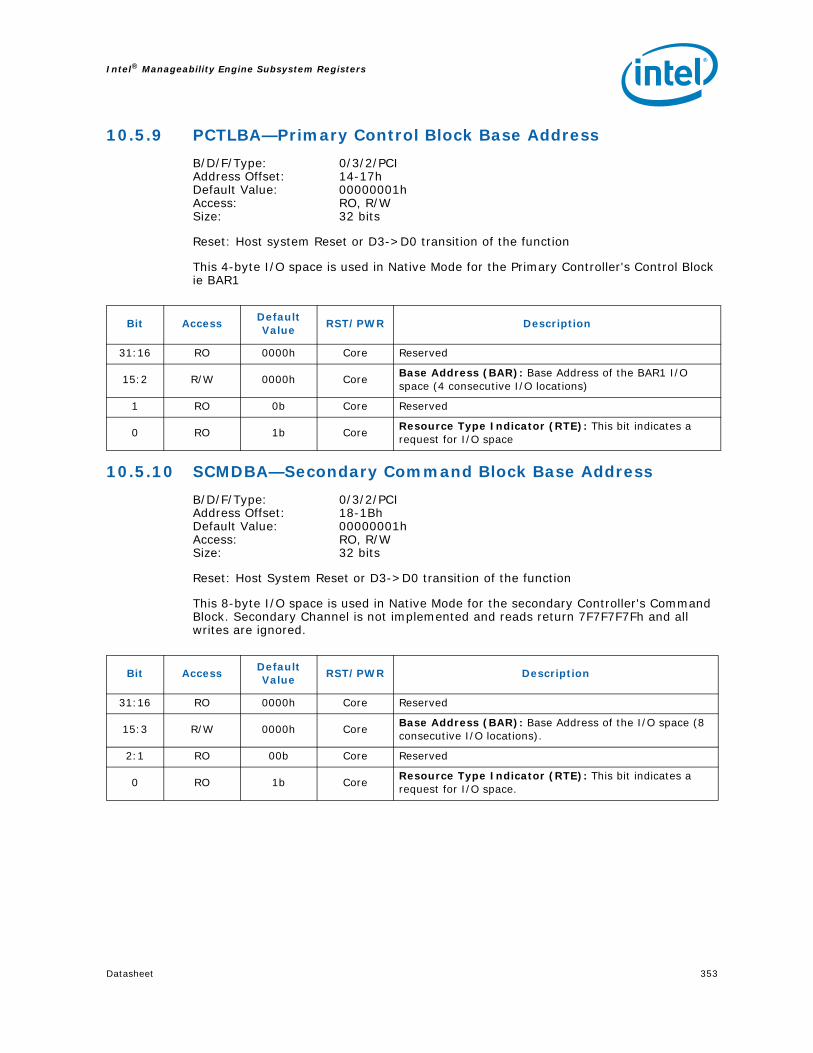
Datasheet 353
Intel® Manageability Engine Subsystem Registers
10.5.9 PCTLBA—Primary Control Block Base Address
B/D/F/Type: 0/3/2/PCIAddress Offset: 14-17hDefault Value: 00000001hAccess: RO, R/WSize: 32 bits
Reset: Host system Reset or D3->D0 transition of the function
This 4-byte I/O space is used in Native Mode for the Primary Controller's Control Block ie BAR1
10.5.10 SCMDBA—Secondary Command Block Base Address
B/D/F/Type: 0/3/2/PCIAddress Offset: 18-1BhDefault Value: 00000001hAccess: RO, R/WSize: 32 bits
Reset: Host System Reset or D3->D0 transition of the function
This 8-byte I/O space is used in Native Mode for the secondary Controller's Command Block. Secondary Channel is not implemented and reads return 7F7F7F7Fh and all writes are ignored.
Bit AccessDefault Value
RST/PWR Description
31:16 RO 0000h Core Reserved
15:2 R/W 0000h CoreBase Address (BAR): Base Address of the BAR1 I/O space (4 consecutive I/O locations)
1 RO 0b Core Reserved
0 RO 1b CoreResource Type Indicator (RTE): This bit indicates a request for I/O space
Bit AccessDefault Value
RST/PWR Description
31:16 RO 0000h Core Reserved
15:3 R/W 0000h CoreBase Address (BAR): Base Address of the I/O space (8 consecutive I/O locations).
2:1 RO 00b Core Reserved
0 RO 1b CoreResource Type Indicator (RTE): This bit indicates a request for I/O space.

Intel® Manageability Engine Subsystem Registers
354 Datasheet
10.5.11 SCTLBA—Secondary Control Block base Address
B/D/F/Type: 0/3/2/PCIAddress Offset: 1C-1FhDefault Value: 00000001hAccess: RO, R/WSize: 32 bits
Reset: Host System Reset or D3->D0 transition
This 4-byte I/O space is used in Native Mode for Secondary Controller's Control block. Secondary Channel is not implemented and reads return 7F7F7F7Fh and all writes are ignored.
10.5.12 LBAR—Legacy Bus Master Base Address
B/D/F/Type: 0/3/2/PCIAddress Offset: 20-23hDefault Value: 00000001hAccess: RO, R/WSize: 32 bits
Reset: Host system Reset or D3->D0 transition
This Bar is used to allocate I/O space for the SFF-8038i mode of operation (aka Bus Master IDE).
Bit AccessDefault Value
RST/PWR Description
31:16 RO 0000h Core Reserved
15:2 R/W 0000h CoreBase Address (BAR): Base Address of the I/O space (4 consecutive I/O locations).
1 RO 0b Core Reserved
0 RO 1b CoreResource Type Indicator (RTE): This bit indicates a request for I/O space.
Bit AccessDefault Value
RST/PWR Description
31:16 RO 0000h Core Reserved
15:4 R/W 000h CoreBase Address (BA): Base Address of the I/O space (16 consecutive I/O locations).
3:1 RO 000b Core Reserved
0 RO 1b CoreResource Type Indicator (RTE): This bit indicates a request for I/O space.

Datasheet 355
Intel® Manageability Engine Subsystem Registers
10.5.13 SS—Sub System Identifiers
B/D/F/Type: 0/3/2/PCIAddress Offset: 2C-2FhDefault Value: 00008086hAccess: R/WOSize: 32 bits
Reset: Host System Reset
These registers are used to uniquely identify the add-in card or the subsystem that the device resides within.
10.5.14 EROM—Expansion ROM Base Address
B/D/F/Type: 0/3/2/PCIAddress Offset: 30-33hDefault Value: 00000000hAccess: ROSize: 32 bits
This optional register is not implemented.
10.5.15 CAP—Capabilities Pointer
B/D/F/Type: 0/3/2/PCIAddress Offset: 34hDefault Value: C8hAccess: ROSize: 8 bits
This optional register is used to point to a linked list of new capabilities implemented by the device.
Bit AccessDefault Value
RST/PWR Description
31:16 R/WO 0000h CoreSubsystem ID (SSID): This is written by BIOS. No hardware action taken on this value
15:0 R/WO 8086h CoreSubsystem Vendor ID (SSVID): This is written by BIOS. No hardware action taken on this value
Bit AccessDefault Value
RST/PWR Description
31:11 RO 000000h Core Expansion ROM Base Address (ERBAR):
10:1 RO 000h Core Reserved
0 RO 0b Core Enable (EN): Enable expansion ROM Access.
Bit AccessDefault Value
RST/PWR Description
7:0 RO c8h CoreCapability Pointer (CP): This field indicates that the first capability pointer is offset C8h (the power management capability).

Intel® Manageability Engine Subsystem Registers
356 Datasheet
10.5.16 INTR—Interrupt Information
B/D/F/Type: 0/3/2/PCIAddress Offset: 3C-3DhDefault Value: 0300hAccess: R/W, ROSize: 16 bits
Reset: Host System Reset or D3->D0 reset of the function
See definitions in the registers below
10.5.17 MGNT—Minimum Grant
B/D/F/Type: 0/3/2/PCIAddress Offset: 3EhDefault Value: 00hAccess: ROSize: 8 bits
This optional register is not implemented.
10.5.18 MLAT—Maximum Latency
B/D/F/Type: 0/3/2/PCIAddress Offset: 3FhDefault Value: 00hAccess: ROSize: 8 bits
This optional register is not implemented.
Bit AccessDefault Value
RST/PWR Description
15:8 RO 03h Core
Interrupt Pin (IPIN): A value of 0x1/0x2/0x3/0x4 indicates that this function implements legacy interrupt on INTA/INTB/INTC/INTD, respectivelyFunction Value INTx(2 IDE) 03h INTC
7:0 R/W 00h Core
Interrupt Line (ILINE): The value written in this register indicates which input of the system interrupt controller, the device's interrupt pin is connected to. This value is used by the OS and the device driver, and has no affect on the hardware.
Bit AccessDefault Value
RST/PWR Description
7:0 RO 00h Core Reserved
Bit AccessDefault Value
RST/PWR Description
7:0 RO 00h Core Reserved

Datasheet 357
Intel® Manageability Engine Subsystem Registers
10.5.19 PID—PCI Power Management Capability ID
B/D/F/Type: 0/3/2/PCIAddress Offset: C8-C9hDefault Value: D001hAccess: ROSize: 16 bits
10.5.20 PC—PCI Power Management Capabilities
B/D/F/Type: 0/3/2/PCIAddress Offset: CA-CBhDefault Value: 0023hAccess: ROSize: 16 bits
This register implements the power management capabilities of the function.
Bit AccessDefault Value
RST/PWR Description
15:8 RO D0h CoreNext Capability (NEXT): Its value of D0h points to the MSI capability.
7:0 RO 01h CoreCap ID (CID): This field indicates that this pointer is a PCI power management.
Bit AccessDefault Value
RST/PWR Description
15:11 RO 00000b CorePME Support (PME): This field indicates no PME# in the PT function
10 RO 0b Core D2 Support (D2S): The D2 state is not Supported
9 RO 0b Core D1 Support (D1S): The D1 state is not supported
8:6 RO 000b CoreAux Current (AUXC): PME# from D3 (cold) state is not supported, therefore this field is 000b
5 RO 1b CoreDevice Specific Initialization (DSI): This bit indicates that no device-specific initialization is required.
4 RO 0b Core Reserved
3 RO 0b CorePME Clock (PMEC): This bit indicates that PCI clock is not required to generate PME#.
2:0 RO 011b CoreVersion (VS): This field indicates support for revision 1.2 of the PCI Power Management Specification.

Intel® Manageability Engine Subsystem Registers
358 Datasheet
10.5.21 PMCS—PCI Power Management Control and Status
B/D/F/Type: 0/3/2/PCIAddress Offset: CC-CFhDefault Value: 00000000hAccess: RO, R/W, RO/VSize: 32 bitsBIOS Optimal Default 0000h
Reset: Host System Reset or D3->D0 transition
This register implements the PCI PM Control and Status Register to allow PM state transitions and Wake up
Note: NSR bit of this register. All registers (PCI configuration and Device Specific) marked with D3->D0 transition reset will only do so if the NSR bit reads a 0. If this bit is a 1, the D3->D0 transition will not reset the registers.
Bit AccessDefault Value
RST/PWR Description
31:16 RO 0h Reserved
15 RO 0b CorePME Status (PMES): This bit is set when a PME event is to be requested. Not supported
14:9 RO 00h Core Reserved
8 RO 0b Core PME Enable (PMEE): Not Supported
7:4 RO 0000b Core Reserved
3 RO/V 0b Core
No Soft Reset (NSR): When set to 1, this bit indicates that devices transitioning from D3hot to D0 because of PowerState commands do not perform an internal reset. Configuration Context is preserved. Upon transition from the D3hot to the D0 Initialized state, no additional operating system intervention is required to preserve Configuration Context beyond writing the PowerState bits.When cleared to 0, devices do perform an internal reset upon transitioning from D3hot to D0 via software control of the PowerState bits. Configuration Context is lost when performing the soft reset. Upon transition from the D3hot to the D0 state, full re-initialization sequence is needed to return the device to D0 Initialized.Value in this bit is reflects chicken bit in ME-AUX register x13900, bit [7] which is as follows:0 = Device performs internal reset1 = Device does not perform internal reset
2 RO 0b Core Reserved
1:0 R/W 00b Core
Power State (PS): This field is used both to determine the current power state of the PT function and to set a new power state. The values are:00 = D0 state11 = D3HOT stateWhen in the D3HOT state, the controller's configuration space is available, but the I/O and memory spaces are not. Additionally, interrupts are blocked. If software attempts to write a '10' or '01' to these bits, the write will be ignored.

Datasheet 359
Intel® Manageability Engine Subsystem Registers
10.5.22 MID—Message Signaled Interrupt Capability ID
B/D/F/Type: 0/3/2/PCIAddress Offset: D0-D1hDefault Value: 0005hAccess: ROSize: 16 bits
Message Signalled Interrupt is a feature that allows the device/function to generate an interrupt to the host by performing a DWord memory write to a system specified address with system specified data. This register is used to identify and configure an MSI capable device.
10.5.23 MC—Message Signaled Interrupt Message Control
B/D/F/Type: 0/3/2/PCIAddress Offset: D2-D3hDefault Value: 0080hAccess: RO, R/WSize: 16 bits
Reset: Host System Reset or D3->D0 transition
This register provides System Software control over MSI.
Bit AccessDefault Value
RST/PWR Description
15:8 RO 00h CoreNext Pointer (NEXT): This value indicates this is the last item in the capabilities list.
7:0 RO 05h CoreCapability ID (CID): The Capabilities ID value indicates device is capable of generating an MSI.
Bit AccessDefault Value
RST/PWR Description
15:8 RO 00h Core Reserved
7 RO 1b Core64 Bit Address Capable (C64): Capable of generating 64-bit and 32-bit messages.
6:4 R/W 000b CoreMultiple Message Enable (MME): These bits are R/W for software compatibility, but only one message is ever sent by the PT function.
3:1 RO 000b CoreMultiple Message Capable (MMC): Only one message is required.
0 R/W 0b CoreMSI Enable (MSIE): If set, MSI is enabled and traditional interrupt pins are not used to generate interrupts.

Intel® Manageability Engine Subsystem Registers
360 Datasheet
10.5.24 MA—Message Signaled Interrupt Message Address
B/D/F/Type: 0/3/2/PCIAddress Offset: D4-D7hDefault Value: 00000000hAccess: R/W, ROSize: 32 bits
Reset: Host system Reset or D3->D0 transition
This register specifies the DWORD aligned address programmed by system software for sending MSI.
10.5.25 MAU—Message Signaled Interrupt Message Upper Address
B/D/F/Type: 0/3/2/PCIAddress Offset: D8-DBhDefault Value: 00000000hAccess: RO, R/WSize: 32 bits
Reset: Host system Reset or D3->D0 transition
Upper 32 bits of the message address for the 64bit address capable device.
10.5.26 MD—Message Signaled Interrupt Message Data
B/D/F/Type: 0/3/2/PCIAddress Offset: DC-DDhDefault Value: 0000hAccess: R/WSize: 16 bits
Reset: Host system Reset or D3->D0 transition
This 16-bit field is programmed by system software if MSI is enabled.
Bit AccessDefault Value
RST/PWR Description
31:2 R/W 00000000h CoreAddress (ADDR): This field contains the Lower 32 bits of the system specified message address, always DWord aligned
1:0 RO 00b Core Reserved
Bit AccessDefault Value
RST/PWR Description
31:4 RO 0000000h Core Reserved
3:0 R/W 0000b CoreAddress (ADDR): This field contains the Upper 4 bits of the system specified message address.
Bit AccessDefault Value
RST/PWR Description
15:0 R/W 0000h CoreData (DATA): This content is driven onto the lower word of the data bus of the MSI memory write transaction.
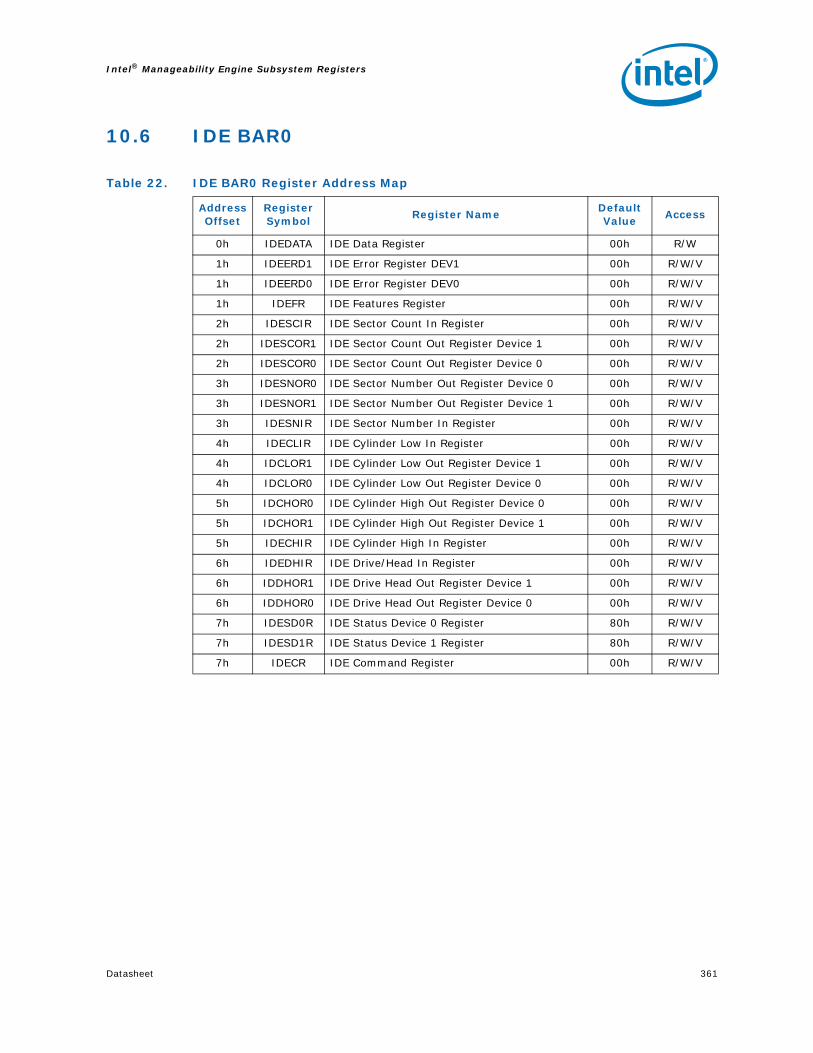
Datasheet 361
Intel® Manageability Engine Subsystem Registers
10.6 IDE BAR0
Table 22. IDE BAR0 Register Address Map
Address Offset
Register Symbol
Register NameDefault Value
Access
0h IDEDATA IDE Data Register 00h R/W
1h IDEERD1 IDE Error Register DEV1 00h R/W/V
1h IDEERD0 IDE Error Register DEV0 00h R/W/V
1h IDEFR IDE Features Register 00h R/W/V
2h IDESCIR IDE Sector Count In Register 00h R/W/V
2h IDESCOR1 IDE Sector Count Out Register Device 1 00h R/W/V
2h IDESCOR0 IDE Sector Count Out Register Device 0 00h R/W/V
3h IDESNOR0 IDE Sector Number Out Register Device 0 00h R/W/V
3h IDESNOR1 IDE Sector Number Out Register Device 1 00h R/W/V
3h IDESNIR IDE Sector Number In Register 00h R/W/V
4h IDECLIR IDE Cylinder Low In Register 00h R/W/V
4h IDCLOR1 IDE Cylinder Low Out Register Device 1 00h R/W/V
4h IDCLOR0 IDE Cylinder Low Out Register Device 0 00h R/W/V
5h IDCHOR0 IDE Cylinder High Out Register Device 0 00h R/W/V
5h IDCHOR1 IDE Cylinder High Out Register Device 1 00h R/W/V
5h IDECHIR IDE Cylinder High In Register 00h R/W/V
6h IDEDHIR IDE Drive/Head In Register 00h R/W/V
6h IDDHOR1 IDE Drive Head Out Register Device 1 00h R/W/V
6h IDDHOR0 IDE Drive Head Out Register Device 0 00h R/W/V
7h IDESD0R IDE Status Device 0 Register 80h R/W/V
7h IDESD1R IDE Status Device 1 Register 80h R/W/V
7h IDECR IDE Command Register 00h R/W/V

Intel® Manageability Engine Subsystem Registers
362 Datasheet
10.6.1 IDEDATA—IDE Data Register
B/D/F/Type: 0/3/2/IDE IO BAR0Address Offset: 0hDefault Value: 00hAccess: R/WSize: 8 bits
The IDE data interface is a special interface that is implemented in the HW. This data interface is mapped to IO space from the host and takes read and write cycles from the host targeting master or slave device.
Writes from host to this register result in the data being written to ME memory.
Reads from host to this register result in the data being fetched from ME memory.
Data is typically written/ read in WORD's. ME-FW must enable hardware to allow it to accept Host initiated Read/ Write cycles, else the cycles are dropped.
10.6.2 IDEERD1—IDE Error Register Device 1
B/D/F/Type: 0/3/2/IDE IO BAR0Address Offset: 1hDefault Value: 00hAccess: R/W/VSize: 8 bits
Reset: Host system reset or D3->D0 transition
This register implements the Error register of the command block of the IDE function. This register is read only by the HOST interface when DEV = 1 (slave device).
When the HOST writes the same address it writes to the Features register.
Bit AccessDefault Value
RST/PWR Description
7:0 R/W 00h Core
IDE Data Register (IDEDR): Data Register implements the data interface for IDE. All writes and reads to this register translate into one or more corresponding write/reads to ME memory
Bit AccessDefault Value
RST/PWR Description
7:0 R/W/V 00h CoreIDE Error Data (IDEED): Drive reflects its error/ diagnostic code to the host via this register at different times.

Datasheet 363
Intel® Manageability Engine Subsystem Registers
10.6.3 IDEERD0—IDE Error Register DEV0
B/D/F/Type: 0/3/2/IDE IO BAR0Address Offset: 1hDefault Value: 00hAccess: R/W/VSize: 8 bits
Reset: Host system reset or D3->D0 transition
This register implements the Error register of the command block of the IDE function. This register is read only by the HOST interface when DEV = 0 (master device).
When the HOST writes the same address it writes to the Features register.
10.6.4 IDEFR—IDE Features Register
B/D/F/Type: 0/3/2/IDE IO BAR0Address Offset: 1hDefault Value: 00hAccess: R/W/VSize: 8 bits
Reset: Host system Reset or D3->D0 transition
This register implements the Feature register of the command block of the IDE function. This register can be written only by the Host.
When the HOST reads the same address, it reads the Error register of Device 0 or Device 1 depending on the device_select bit (bit 4 of the drive/head register).
Bit AccessDefault Value
RST/PWR Description
7:0 R/W/V 00h CoreIDE Error Data (IDEED): Drive reflects its error/ diagnostic code to the host via this register at different times.
Bit AccessDefault Value
RST/PWR Description
7:0 R/W/V 00h CoreIDE Feature Data (IDEFD): IDE drive specific data written by the Host

Intel® Manageability Engine Subsystem Registers
364 Datasheet
10.6.5 IDESCIR—IDE Sector Count In Register
B/D/F/Type: 0/3/2/IDE IO BAR0Address Offset: 2hDefault Value: 00hAccess: R/W/VSize: 8 bits
Reset: Host system Reset or D3->D0 transition
This register implements the Sector Count register of the command block of the IDE function. This register can be written only by the Host. When host writes to this register, all 3 registers (IDESCIR, IDESCOR0, IDESCOR1) are updated with the written value.
A host read to this register address reads the IDE Sector Count Out Register IDESCOR0 if DEV=0 or IDESCOR1 if DEV=1
10.6.6 IDESCOR1—IDE Sector Count Out Register Dev1
B/D/F/Type: 0/3/2/IDE IO BAR0Address Offset: 2hDefault Value: 00hAccess: R/W/VSize: 8 bits
Reset: Host system Reset or D3->D0 transition
This register is read by the HOST interface if DEV = 1. ME-Firmware writes to this register at the end of a command of the selected device.
When the host writes to this address, the IDE Sector Count In Register (IDESCIR), this register is updated.
Bit AccessDefault Value
RST/PWR Description
7:0 R/W/V 00h CoreIDE Sector Count Data (IDESCD): Host writes the number of sectors to be read or written.
Bit AccessDefault Value
RST/PWR Description
7:0 R/W/V 00h CoreIDE Sector Count Out Dev1 (ISCOD1): Sector Count register for Slave Device ie Device 1

Datasheet 365
Intel® Manageability Engine Subsystem Registers
10.6.7 IDESCOR0—IDE Sector Count Out Register Device 0
B/D/F/Type: 0/3/2/IDE IO BAR0Address Offset: 2hDefault Value: 00hAccess: R/W/VSize: 8 bits
Reset: Host system Reset or D3->D0 transition
This register is read by the HOST interface if DEV = 0. ME-Firmware writes to this register at the end of a command of the selected device.
When the host writes to this address, the IDE Sector Count In Register (IDESCIR), this register is updated.
10.6.8 IDESNOR0—IDE Sector Number Out Register Device 0
B/D/F/Type: 0/3/2/IDE IO BAR0Address Offset: 3hDefault Value: 00hAccess: R/W/VSize: 8 bits
Reset: Host system Reset or D3->D0 transition
This register is read by the Host if DEV = 0. ME-Firmware writes to this register at the end of a command of the selected device.
When the host writes to the IDE Sector Number In Register (IDESNIR), this register is updated with that value.
Bit AccessDefault Value
RST/PWR Description
7:0 R/W/V 00h CoreIDE Sector Count Out Dev0 (ISCOD0): Sector Count register for Master Device ie Device 0.
Bit AccessDefault Value
RST/PWR Description
7:0 R/W/V 00h CoreIDE Sector Number Out DEV 0 (IDESNO0): Sector Number Out register for Master device.

Intel® Manageability Engine Subsystem Registers
366 Datasheet
10.6.9 IDESNOR1—IDE Sector Number Out Register Device 1
B/D/F/Type: 0/3/2/IDE IO BAR0Address Offset: 3hDefault Value: 00hAccess: R/W/VSize: 8 bits
Reset: Host system Reset or D3->D0 transition
This register is read by the Host if DEV = 1. ME-Firmware writes to this register at the end of a command of the selected device.
When the host writes to the IDE Sector Number In Register (IDESNIR), this register is updated with that value.
10.6.10 IDESNIR—IDE Sector Number In Register
B/D/F/Type: 0/3/2/IDE IO BAR0Address Offset: 3hDefault Value: 00hAccess: R/W/VSize: 8 bits
Reset: Host system Reset or D3->D0 transition
This register implements the Sector Number register of the command block of the IDE function. This register can be written only by the Host. When host writes to this register, all 3 registers (IDESNIR, IDESNOR0, IDESNOR1) are updated with the written value.
Host read to this register address reads the IDE Sector Number Out Register IDESNOR0 if DEV=0 or IDESNOR1 if DEV=1.
Bit AccessDefault Value
RST/PWR Description
7:0 R/W/V 00h CoreIDE Sector Number Out DEV 1 (IDESNO1): Sector Number Out register for Slave device.
Bit AccessDefault Value
RST/PWR Description
7:0 R/W/V 00h CoreIDE Sector Number Data (IDESND): This register contains the number of the first sector to be transferred.

Datasheet 367
Intel® Manageability Engine Subsystem Registers
10.6.11 IDECLIR—IDE Cylinder Low In Register
B/D/F/Type: 0/3/2/IDE IO BAR0Address Offset: 4hDefault Value: 00hAccess: R/W/VSize: 8 bits
Reset: Host system Reset or D3->D0 transition
This register implements the Cylinder Low register of the command block of the IDE function. This register can be written only by the Host. When host writes to this register, all 3 registers (IDECLIR, IDECLOR0, IDECLOR1) are updated with the written value.
Host read to this register address reads the IDE Cylinder Low Out Register IDECLOR0 if DEV=0 or IDECLOR1 if DEV=1.
10.6.12 IDCLOR1—IDE Cylinder Low Out Register Device 1
B/D/F/Type: 0/3/2/IDE IO BAR0Address Offset: 4hDefault Value: 00hAccess: R/W/VSize: 8 bits
Reset: Host system Reset or D3->D0 transition
This register is read by the Host if DEV = 1. ME-Firmware writes to this register at the end of a command of the selected device. When the host writes to the IDE Cylinder Low In Register (IDECLIR), this register is updated with that value.
Bit AccessDefault Value
RST/PWR Description
7:0 R/W/V 00h CoreIDE Cylinder Low Data (IDECLD): Cylinder Low register of the command block of the IDE function.
Bit AccessDefault Value
RST/PWR Description
7:0 R/W/V 00h CoreIDE Cylinder Low Out DEV 1. (IDECLO1): Cylinder Low Out Register for Slave Device.

Intel® Manageability Engine Subsystem Registers
368 Datasheet
10.6.13 IDCLOR0—IDE Cylinder Low Out Register Device 0
B/D/F/Type: 0/3/2/IDE IO BAR0Address Offset: 4hDefault Value: 00hAccess: R/W/VSize: 8 bits
Reset: Host system Reset or D3->D0 transition
This register is read by the Host if DEV = 0. ME-Firmware writes to this register at the end of a command of the selected device. When the host writes to the IDE Cylinder Low In Register (IDECLIR), this register is updated with that value.
10.6.14 IDCHOR0—IDE Cylinder High Out Register Device 0
B/D/F/Type: 0/3/2/IDE IO BAR0Address Offset: 5hDefault Value: 00hAccess: R/W/VSize: 8 bits
Reset: Host system Reset or D3->D0 transition
This register is read by the Host if DEVice = 0. ME-Firmware writes to this register at the end of a command of the selected device. When the host writes to the IDE Cylinder High In Register (IDECHIR), this register is updated with that value.
Bit AccessDefault Value
RST/PWR Description
7:0 R/W/V 00h CoreIDE Cylinder Low Out DEV 0. (IDECLO0): Cylinder Low Out Register for Master Device.
Bit AccessDefault Value
RST/PWR Description
7:0 R/W/V 00h CoreIDE Cylinder High Out DEV 0 (IDECHO0): Cylinder High out register for Master device.

Datasheet 369
Intel® Manageability Engine Subsystem Registers
10.6.15 IDCHOR1—IDE Cylinder High Out Register Device 1
B/D/F/Type: 0/3/2/IDE IO BAR0Address Offset: 5hDefault Value: 00hAccess: R/W/VSize: 8 bits
Reset: Host system Reset or D3->D0 transition
This register is read by the Host if Device = 1. ME-Firmware writes to this register at the end of a command of the selected device. When the host writes to the IDE Cylinder High In Register (IDECHIR), this register is updated with that value.
10.6.16 IDECHIR—IDE Cylinder High In Register
B/D/F/Type: 0/3/2/IDE IO BAR0Address Offset: 5hDefault Value: 00hAccess: R/W/VSize: 8 bits
Reset: Host system Reset or D3->D0 transition
This register implements the Cylinder High register of the command block of the IDE function. This register can be written only by the Host. When host writes to this register, all 3 registers (IDECHIR, IDECHOR0, IDECHOR1) are updated with the written value.
Host read to this register address reads the IDE Cylinder High Out Register IDECHOR0 if DEV=0 or IDECHOR1 if DEV=1.
Bit AccessDefault Value
RST/PWR Description
7:0 R/W/V 00h Core IDE Cylinder High Out DEV 1 (IDECHO1): Cylinder High out register for Slave device.
Bit AccessDefault Value
RST/PWR Description
7:0 R/W/V 00h CoreIDE Cylinder High Data (IDECHD): Cylinder High data register for IDE command block.

Intel® Manageability Engine Subsystem Registers
370 Datasheet
10.6.17 IDEDHIR—IDE Drive/Head In Register
B/D/F/Type: 0/3/2/IDE IO BAR0Address Offset: 6hDefault Value: 00hAccess: R/W/VSize: 8 bits
Reset: Host system Reset or D3->D0 transition
This register implements the Drive/Head register of the command block of the IDE. This register can be written only by the Host. When host writes to this register, all 3 registers (IDEDHIR, IDEDHOR0, IDEDHOR1) are updated with the written value.
Host read to this register address reads the IDE Drive/Head Out Register (IDEDHOR0) if DEV=0 or IDEDHOR1 if DEV=1.
Bit 4 of this register is the DEV (master/slave) bit. This bit is cleared by hardware on IDE software reset (S_RST toggles to '1') in addition to Host system reset and D3->D0 transition of the function.
10.6.18 IDDHOR1—IDE Drive Head Out Register Device 1
B/D/F/Type: 0/3/2/IDE IO BAR0Address Offset: 6hDefault Value: 00hAccess: R/W/VSize: 8 bits
Reset: Host system Reset or D3->D0 transition
This register is read only by the Host. Host read to this Drive/head In register address reads the IDE Drive/Head Out Register (IDEDHOR0) if DEV=1
Bit 4 of this register is the DEV (master/slave) bit. This bit is cleared by hardware on IDE software reset (S_RST toggles to '1') in addition to the Host system reset and D3 to D0 transition of the IDE function.
When the host writes to this address, it updates the value of the IDEDHIR register.
Bit AccessDefault Value
RST/PWR Description
7:0 R/W/V 00h CoreIDE Drive/Head Data (IDEDHD): Register defines the drive number, head number and addressing mode.
Bit AccessDefault Value
RST/PWR Description
7:0 R/W/V 00h CoreIDE Drive Head Out DEV 1 (IDEDHO1): Drive/Head Out register of Slave device.

Datasheet 371
Intel® Manageability Engine Subsystem Registers
10.6.19 IDDHOR0—IDE Drive Head Out Register Device 0
B/D/F/Type: 0/3/2/IDE IO BAR0Address Offset: 6hDefault Value: 00hAccess: R/W/VSize: 8 bits
Reset: Host system Reset or D3->D0 transition
This register is read only by the Host. Host read to this Drive/head In register address reads the IDE Drive/Head Out Register (IDEDHOR0) if DEV=0.
Bit 4 of this register is the DEV (master/slave) bit. This bit is cleared by hardware on IDE software reset (S_RST toggles to 1) in addition to the Host system reset and D3 to D0 transition of the IDE function.
When the host writes to this address, it updates the value of the IDEDHIR register.
Bit AccessDefault Value
RST/PWR Description
7:0 R/W/V 00h CoreIDE Drive Head Out DEV 0 (IDEDHO0): Drive/Head Out register of Master device.

Intel® Manageability Engine Subsystem Registers
372 Datasheet
10.6.20 IDESD0R—IDE Status Device 0 Register
B/D/F/Type: 0/3/2/IDE IO BAR0Address Offset: 7hDefault Value: 80hAccess: R/W/VSize: 8 bits
Reset: Host system reset or D3->D0 transition
This register implements the status register of the Master device (DEV = 0). This register is read only by the Host. Host read of this register clears the Master device's interrupt.
When the HOST writes to the same address it writes to the command register
The bits description is for ATA mode.
Bit AccessDefault Value
RST/PWR Description
7 R/W/V 1b Core
Busy (BSY): This bit is set by HW when the IDECR is being written and DEV=0, or when SRST bit is asserted by Host or host system reset or D3-to-D0 transition of the IDE function.This bit is cleared by FW write of 0.
6 R/W/V 0b CoreDrive Ready (DRDY): When set, this bit indicates drive is ready for command.
5 R/W/V 0b Core Drive Fault (DF): Indicates Error on the drive.
4 R/W/V 0b CoreDrive Seek Complete (DSC): Indicates Heads are positioned over the desired cylinder.
3 R/W/V 0b CoreData Request (DRQ): Set when, the drive wants to exchange data with the Host via the data register.
2 R/W/V 0b CoreCorrected Data (CORR): When set, this bit indicates a correctable read error has occurred.
1 R/W/V 0b CoreIndex (IDX): This bit is set once per rotation of the medium when the index mark passes under the read/write head.
0 R/W/V 0b Core
Error (ERR): When set, this bit indicates an error occurred in the process of executing the previous command. The Error Register of the selected device contains the error information.

Datasheet 373
Intel® Manageability Engine Subsystem Registers
10.6.21 IDESD1R—IDE Status Device 1 Register
B/D/F/Type: 0/3/2/IDE IO BAR0Address Offset: 7hDefault Value: 80hAccess: R/W/VSize: 8 bits
Reset: Host system reset or D3->D0 transition
This register implements the status register of the slave device (DEV = 1). This register is read only by the Host. Host read of this register clears the slave device's interrupt.
When the HOST writes to the same address it writes to the command register.
The bits description is for ATA mode.
Bit AccessDefault Value
RST/PWR Description
7 R/W/V 1b Core
Busy (BSY): This bit is set by hardware when the IDECR is being written and DEV=0, or when SRST bit is asserted by the Host or host system reset or D3-to-D0 transition of the IDE function.This bit is cleared by FW write of 0.
6 R/W/V 0b CoreDrive Ready (DRDY): When set, indicates drive is ready for command.
5 R/W/V 0b Core Drive Fault (DF): Indicates Error on the drive.
4 R/W/V 0b CoreDrive Seek Complete (DSC): Indicates Heads are positioned over the desired cylinder.
3 R/W/V 0b CoreData Request (DRQ): Set when the drive wants to exchange data with the Host via the data register.
2 R/W/V 0b CoreCorrected Data (CORR): When set indicates a correctable read error has occurred.
1 R/W/V 0b CoreIndex (IDX): This bit is set once per rotation of the medium when the index mark passes under the read/write head.
0 R/W/V 0b Core
Error (ERR): When set, this bit indicates an error occurred in the process of executing the previous command. The Error Register of the selected device contains the error information

Intel® Manageability Engine Subsystem Registers
374 Datasheet
10.6.22 IDECR—IDE Command Register
B/D/F/Type: 0/3/2/IDE IO BAR0Address Offset: 7hDefault Value: 00hAccess: R/W/VSize: 8 bits
Reset: Host system Reset and D3->D0 transition
This register implements the Command register of the command block of the IDE function. This register can be written only by the Host.
When the HOST reads the same address it reads the Status register DEV0 if DEV=0 or Status Register DEV1 if DEV=1 (Drive/Head register bit [4]).
Bit AccessDefault Value
RST/PWR Description
7:0 R/W/V 00h CoreIDE Command Data (IDECD): Host sends the commands (read/ write, etc.) to the drive via this register.

Datasheet 375
Intel® Manageability Engine Subsystem Registers
10.7 IDE BAR1
10.7.1 IDDCR—IDE Device Control Register
B/D/F/Type: 0/3/2/IDE IO BAR1Address Offset: 2hDefault Value: 00hAccess: RO, WOSize: 8 bits
Reset: Host system Reset or D3->D0 transition
This register implements the Device Control register of the Control block of the IDE function. This register is Write only by the Host.
When the HOST reads to the same address it reads the Alternate Status register.
Address Offset
Register Symbol
Register NameDefault Value
Access
2h IDDCR IDE Device Control Register 00h RO, WO
2h IDASR IDE Alternate status Register 00h RO/V
Bit AccessDefault Value
RST/PWR Description
7:3 RO 00000b CoreReserved: Writable by Host, but no hardware affect due to writes.
2 WO 0b Core Software reset (S_RST): When this bit is set by the Host, it forces a reset to the device.
1 WO 0b Core Host interrupt Disable (nIEN): When set, this bit disables hardware from sending interrupt to the Host.
0 RO 0b CoreReserved: Writable by Host, but no hardware affect due to writes

Intel® Manageability Engine Subsystem Registers
376 Datasheet
10.7.2 IDASR—IDE Alternate status Register
B/D/F/Type: 0/3/2/IDE IO BAR1Address Offset: 2hDefault Value: 00hAccess: RO/VSize: 8 bits
Reset: This is not a physical register hence no reset associated with it.
This register implements the Alternate Status register of the Control block of the IDE function. This register is a mirror register to the status register in the command block. Reading this register by the HOST does not clear the IDE interrupt of the DEV selected device
Host read of this register when DEV=0 (Master), Host gets the mirrored data of IDESD0R register.
Host read of this register when DEV=1 (Slave), host gets the mirrored data of IDESD1R register.
Bit AccessDefault Value
RST/PWR Description
7:0 RO/V 00h CoreIDE Alternate Status Register (IDEASR): This field mirrors the value of the DEV0/ DEV1 status register, depending on the state of the DEV bit on Host reads.

Datasheet 377
Intel® Manageability Engine Subsystem Registers
10.8 IDE BAR4
Table 23. IDE BAR4 Register Address Map
Address Offset
Register Symbol
Register NameDefault Value
Access
0h IDEPBMCRIDE Primary Bus Master Command Register
00h RO, R/W
1h IDEPBMDS0RIDE Primary Bus Master Device Specific 0 Register
00h R/W
2h IDEPBMSR IDE Primary Bus Master Status Register 80h RO, R/W,
R/WC
3h IDEPBMDS1RIDE Primary Bus Master Device Specific 1 Register
00h R/W
4h IDEPBMDTPR0IDE Primary Bus Master Descriptor Table Pointer Register Byte 0
00h R/W
5h IDEPBMDTPR1IDE Primary Bus Master Descriptor Table Pointer Register Byte 1
00h R/W
6h IDEPBMDTPR2IDE Primary Bus Master Descriptor Table Pointer Register Byte 2
00h R/W
7h IDEPBMDTPR3IDE Primary Bus Master Descriptor Table Pointer Register Byte 3
00h R/W
8h IDESBMCRIDE Secondary Bus Master Command Register
00h RO, R/W
9h IDESBMDS0RIDE Secondary Bus Master Device Specific 0 Register
00h R/W
Ah IDESBMSRIDE Secondary Bus Master Status Register
00h R/W, RO
Bh IDESBMDS1RIDE Secondary Bus Master Device Specific 1 Register
00h R/W
Ch IDESBMDTPR0IDE Secondary Bus Master Descriptor Table Pointer Register Byte 0
00h R/W
Dh IDESBMDTPR1IDE Secondary Bus Master Descriptor Table Pointer Register Byte 1
00h R/W
Eh IDESBMDTPR2IDE Secondary Bus Master Descriptor Table Pointer Register Byte 2
00h R/W
Fh IDESBMDTPR3IDE Secondary Bus Master Descriptor Table Pointer Register Byte 3
00h R/W

Intel® Manageability Engine Subsystem Registers
378 Datasheet
10.8.1 IDEPBMCR—IDE Primary Bus Master Command Register
B/D/F/Type: 0/3/2/IDE IO BAR4Address Offset: 0hDefault Value: 00hAccess: RO, R/WSize: 8 bits
Reset: See specific bits.
This register implements the bus master command register of the primary channel. This register is programmed by the Host.
10.8.2 IDEPBMDS0R—IDE Primary Bus Master Device Specific 0 Register
B/D/F/Type: 0/3/2/IDE IO BAR4Address Offset: 1hDefault Value: 00hAccess: R/WSize: 8 bits
Reset: ME System Reset
This register implements the bus master Device Specific 1 register of the primary channel. This register is programmed by the Host.
Bit AccessDefault Value
RST/PWR Description
7:4 RO 0h Core Reserved
3 R/W 0b Core
Read Write Command (RWC): This bit sets the direction of bus master transfer. 0 = Reads are performed from system memory1 = Writes are performed to System Memory. This bit should not be changed when the bus master function is active.Reset: Host system Reset or D3->D0 transition
2:1 RO 00b Core Reserved
0 R/W 0b Core
Start/Stop Bus Master (SSBM): This bit gates the bus master operation of IDE function when 0. Writing 1 enables the bus master operation. Bus master operation can be halted by writing a 0 to this bit. Operation cannot be stopped and resumed.This bit is cleared after data transfer is complete as indicated by either the BMIA bit or the INT bit of the Bus Master status register is set or both are set.Reset: Host system Reset or D3->D0 transition.
Bit AccessDefault Value
RST/PWR Description
7:0 R/W 00h Core Device Specific Data0 (DSD0): Device Specific

Datasheet 379
Intel® Manageability Engine Subsystem Registers
10.8.3 IDEPBMSR—IDE Primary Bus Master Status Register
B/D/F/Type: 0/3/2/IDE IO BAR4Address Offset: 2hDefault Value: 80hAccess: RO, R/W, R/WCSize: 8 bits
Reset: See bit definitions.
This register implements the Bus Master Status register of the primary channel.
Bit AccessDefault Value
RST/PWR Description
7 RO 1b Core
Simplex Only (SO): Value indicates whether both Bus Master Channels can be operated at the same time or not.0 = Both can be operated independently1 = Only one can be operated at a time.Reset: ME System Reset
6 R/W 0b Core
Drive 1 DMA Capable (D1DC): This bit is read/write by the host (not write 1 clear).Reset: Host system Reset or D3->D0 transition of the function
5 R/W 0b Core
Drive 0 DMA Capable (D0DC): This bit is read/write by the host (not write 1 clear).Reset: Host system Reset or D3->D0 transition of the function
4:3 RO 00b Core Reserved
2 R/WC 0b Core
Interrupt (INT): This bit is set by the hardware when it detects a positive transition in the interrupt logic (refer to IDE host interrupt generation diagram).The hardware will clear this bit when the Host SW writes 1 to it.Reset: ME System Reset
1 R/WC 0b CoreError (ER): Bit is typically set by FW. Hardware will clear this bit when the Host SW writes 1 to it.Reset: ME System Reset
0 RO 0b Core
Bus Master IDE Active (BMIA): This bit is set by hardware when SSBM register is set to 1 by the Host. When the bus master operation ends (for the whole command) this bit is cleared by FW. This bit is not cleared when the HOST writes 1 to it.Reset: ME system Reset

Intel® Manageability Engine Subsystem Registers
380 Datasheet
10.8.4 IDEPBMDS1R—IDE Primary Bus Master Device Specific 1 Register
B/D/F/Type: 0/3/2/IDE IO BAR4Address Offset: 3hDefault Value: 00hAccess: R/WSize: 8 bits
Reset: ME system Reset
This register implements the bus master Device Specific 1 register of the primary channel. This register is programmed by the Host for device specific data if any.
10.8.5 IDEPBMDTPR0—IDE Primary Bus Master Descriptor TablePointer Register Byte 0
B/D/F/Type: 0/3/2/IDE IO BAR4Address Offset: 4hDefault Value: 00hAccess: R/WSize: 8 bits
Reset: Host system Reset or D3->D0 transition
This register implements the Byte 0 (1 of 4 bytes) of the descriptor table Pointer (four I/O byte addresses) for bus master operation of the primary channel. This register is read/write by the HOST interface.
10.8.6 IDEPBMDTPR1—IDE Primary Bus Master Descriptor TablePointer Register Byte 1
B/D/F/Type: 0/3/2/IDE IO BAR4Address Offset: 5hDefault Value: 00hAccess: R/WSize: 8 bits
Reset: Host system Reset or D3->D0 transition
This register implements the Byte 1 (of four bytes) of the descriptor table Pointer (four I/O byte addresses) for bus master operation of the primary channel. This register is programmed by the Host.
Bit AccessDefault Value
RST/PWR Description
7:0 R/W 00h Core Device Specific Data1 (DSD1): Device Specific Data.
Bit AccessDefault Value
RST/PWR Description
7:0 R/W 00h Core Descriptor Table Pointer Byte 0 (DTPB0):
Bit AccessDefault Value
RST/PWR Description
7:0 R/W 00h Core Descriptor Table Pointer Byte 1 (DTPB1):

Datasheet 381
Intel® Manageability Engine Subsystem Registers
10.8.7 IDEPBMDTPR2—IDE Primary Bus Master Descriptor TablePointer Register Byte 2
B/D/F/Type: 0/3/2/IDE IO BAR4Address Offset: 6hDefault Value: 00hAccess: R/WSize: 8 bits
Reset: Host system Reset or D3->D0 transition
This register implements the Byte 2 (of four bytes) of the descriptor table Pointer (four I/O byte addresses) for bus master operation of the primary channel. This register is programmed by the Host.
10.8.8 IDEPBMDTPR3—IDE Primary Bus Master Descriptor TablePointer Register Byte 3
B/D/F/Type: 0/3/2/IDE IO BAR4Address Offset: 7hDefault Value: 00hAccess: R/WSize: 8 bits
Reset: Host system Reset or D3->D0 transition
This register implements the Byte 3 (of four bytes) of the descriptor table Pointer (four I/O byte addresses) for bus master operation of the primary channel. This register is programmed by the Host
Bit AccessDefault Value
RST/PWR Description
7:0 R/W 00h Core Descriptor Table Pointer Byte 2 (DTPB2):
Bit AccessDefault Value
RST/PWR Description
7:0 R/W 00h Core Descriptor Table Pointer Byte 3 (DTPB3):

Intel® Manageability Engine Subsystem Registers
382 Datasheet
10.8.9 IDESBMCR—IDE Secondary Bus Master Command Register
B/D/F/Type: 0/3/2/IDE IO BAR4Address Offset: 8hDefault Value: 00hAccess: RO, R/WSize: 8 bits
Reset: See specific bits
This register implements the bus master command register of the secondary channel. This register is programmed by the Host.
10.8.10 IDESBMDS0R—IDE Secondary Bus Master Device Specific 0 Register
B/D/F/Type: 0/3/2/IDE IO BAR4Address Offset: 9hDefault Value: 00hAccess: R/WSize: 8 bits
Reset: ME System Reset
This register implements the bus master Device Specific 1 register of the secondary channel. This register is programmed by the Host.
Bit AccessDefault Value
RST/PWR Description
7:4 RO 0h Core Reserved
3 R/W 0b Core
Read Write Command (RWC): This bit sets the direction of bus master transfer. When 0, Reads are performed from system memory; when 1, writes are performed to System Memory. This bit should not be changed when the bus master function is active.Reset: Host system Reset or D3->D0 transition of function
2:1 RO 00b Core Reserved
0 R/W 0b Core
Start/Stop Bus Master (SSBM): This bit gates the bus master operation of IDE function when zero.Writing 1 enables the bus master operation. Bus master operation can be halted by writing a 0 to this bit. Operation cannot be stopped and resumed.This bit is cleared after data transfer is complete as indicated by either the BMIA bit or the INT bit of the Bus Master status register is set or both are set.Reset: Host system Reset or D3->D0 transition of function
Bit AccessDefault Value
RST/PWR Description
7:0 R/W 00h Core Device Specific Data0 (DSD0): Device Specific
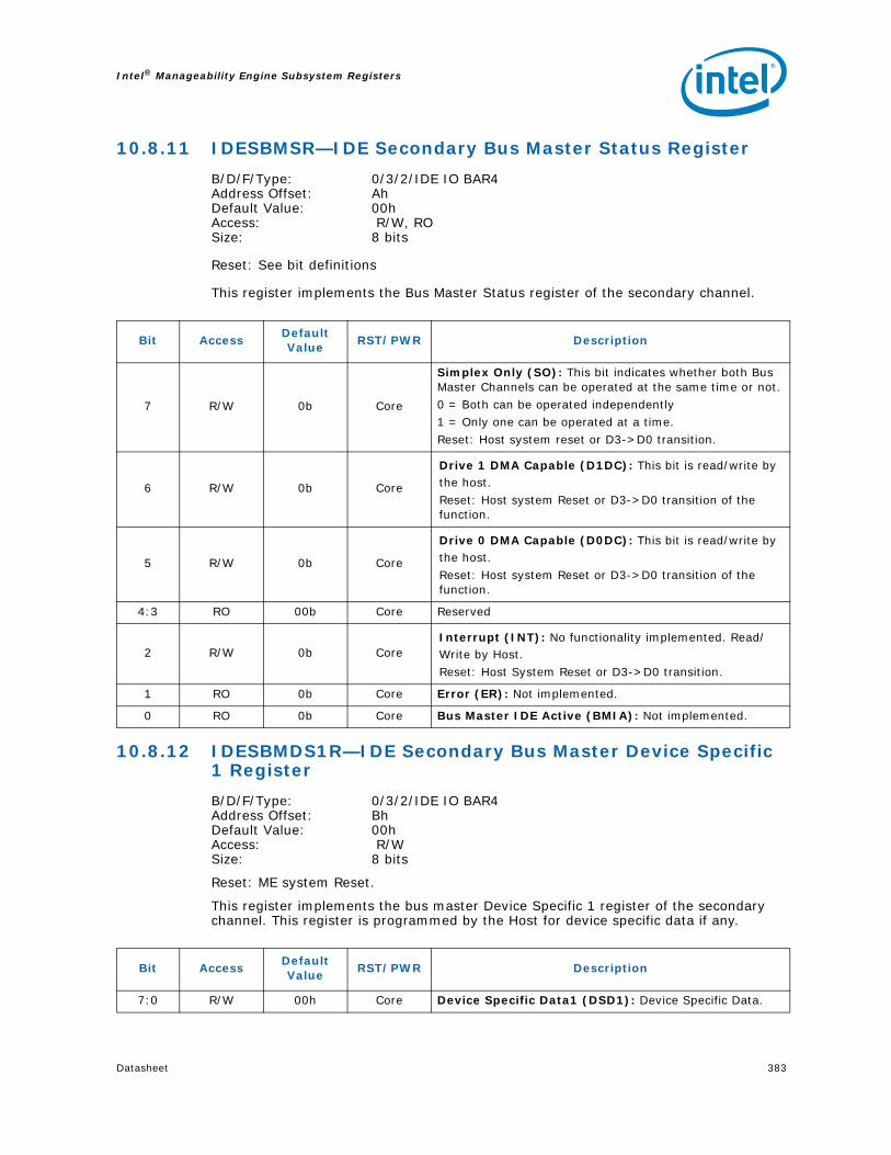
Datasheet 383
Intel® Manageability Engine Subsystem Registers
10.8.11 IDESBMSR—IDE Secondary Bus Master Status Register
B/D/F/Type: 0/3/2/IDE IO BAR4Address Offset: AhDefault Value: 00hAccess: R/W, ROSize: 8 bits
Reset: See bit definitions
This register implements the Bus Master Status register of the secondary channel.
10.8.12 IDESBMDS1R—IDE Secondary Bus Master Device Specific 1 Register
B/D/F/Type: 0/3/2/IDE IO BAR4Address Offset: BhDefault Value: 00hAccess: R/WSize: 8 bits
Reset: ME system Reset.
This register implements the bus master Device Specific 1 register of the secondary channel. This register is programmed by the Host for device specific data if any.
Bit AccessDefault Value
RST/PWR Description
7 R/W 0b Core
Simplex Only (SO): This bit indicates whether both Bus Master Channels can be operated at the same time or not.0 = Both can be operated independently1 = Only one can be operated at a time.Reset: Host system reset or D3->D0 transition.
6 R/W 0b Core
Drive 1 DMA Capable (D1DC): This bit is read/write by the host.
Reset: Host system Reset or D3->D0 transition of the function.
5 R/W 0b Core
Drive 0 DMA Capable (D0DC): This bit is read/write by the host.Reset: Host system Reset or D3->D0 transition of the function.
4:3 RO 00b Core Reserved
2 R/W 0b CoreInterrupt (INT): No functionality implemented. Read/ Write by Host. Reset: Host System Reset or D3->D0 transition.
1 RO 0b Core Error (ER): Not implemented.
0 RO 0b Core Bus Master IDE Active (BMIA): Not implemented.
Bit AccessDefault Value
RST/PWR Description
7:0 R/W 00h Core Device Specific Data1 (DSD1): Device Specific Data.
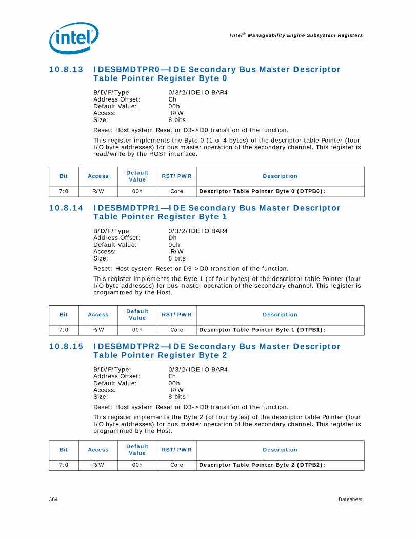
Intel® Manageability Engine Subsystem Registers
384 Datasheet
10.8.13 IDESBMDTPR0—IDE Secondary Bus Master Descriptor Table Pointer Register Byte 0
B/D/F/Type: 0/3/2/IDE IO BAR4Address Offset: ChDefault Value: 00hAccess: R/WSize: 8 bits
Reset: Host system Reset or D3->D0 transition of the function.
This register implements the Byte 0 (1 of 4 bytes) of the descriptor table Pointer (four I/O byte addresses) for bus master operation of the secondary channel. This register is read/write by the HOST interface.
10.8.14 IDESBMDTPR1—IDE Secondary Bus Master Descriptor Table Pointer Register Byte 1
B/D/F/Type: 0/3/2/IDE IO BAR4Address Offset: DhDefault Value: 00hAccess: R/WSize: 8 bits
Reset: Host system Reset or D3->D0 transition of the function.
This register implements the Byte 1 (of four bytes) of the descriptor table Pointer (four I/O byte addresses) for bus master operation of the secondary channel. This register is programmed by the Host.
10.8.15 IDESBMDTPR2—IDE Secondary Bus Master Descriptor Table Pointer Register Byte 2
B/D/F/Type: 0/3/2/IDE IO BAR4Address Offset: EhDefault Value: 00hAccess: R/WSize: 8 bits
Reset: Host system Reset or D3->D0 transition of the function.
This register implements the Byte 2 (of four bytes) of the descriptor table Pointer (four I/O byte addresses) for bus master operation of the secondary channel. This register is programmed by the Host.
Bit AccessDefault Value
RST/PWR Description
7:0 R/W 00h Core Descriptor Table Pointer Byte 0 (DTPB0):
Bit AccessDefault Value
RST/PWR Description
7:0 R/W 00h Core Descriptor Table Pointer Byte 1 (DTPB1):
Bit AccessDefault Value
RST/PWR Description
7:0 R/W 00h Core Descriptor Table Pointer Byte 2 (DTPB2):

Datasheet 385
Intel® Manageability Engine Subsystem Registers
10.8.16 IDESBMDTPR3—IDE Secondary Bus Master Descriptor Table Pointer Register Byte 3
B/D/F/Type: 0/3/2/IDE IO BAR4Address Offset: FhDefault Value: 00hAccess: R/WSize: 8 bits
Reset: Host system Reset or D3->D0 transition of the function.
This register implements the Byte 3 (of four bytes) of the descriptor table Pointer (four I/O byte addresses) for bus master operation of the secondary channel. This register is programmed by the Host.
Bit AccessDefault Value
RST/PWR Description
7:0 R/W 00h Core Descriptor Table Pointer Byte 3 (DTPB3):

Intel® Manageability Engine Subsystem Registers
386 Datasheet
10.9 Serial Port for Remote Keyboard and Text (KT) Redirection
Table 24. Serial Port for Remote Keyboard and Text (KT) Redirection Register Address Map
Address Offset
Register Symbol
Register NameDefault Value
Access
0–3h ID Identification 2E078086h RO
4–5h CMD Command Register 0000h RO, R/W
6–7h STS Device Status 00B0h RO
8h RID Revision IDsee register description
RO
9–Bh CC Class Codes 070002h RO
Ch CLS Cache Line Size 00h RO
Dh MLT Master Latency Timer 00h RO
Eh HTYPE Header Type Not Defined Not Defined
Fh BIST Built In Self Test Not Defined Not Defined
10–13h KTIBA KT IO Block Base Address 00000001h RO, R/W
14–17h KTMBA KT Memory Block Base Address 00000000h RO, R/W
2C–2Fh SS Sub System Identifiers 00008086h R/WO
30–33h EROM Expansion ROM Base Address 00000000h RO
34h CAP Capabilities Pointer C8h RO
3C–3Dh INTR Interrupt Information 0200h R/W, RO
3Eh MGNT Minimum Grant 00h RO
3Fh MLAT Maximum Latency 00h RO
C8–C9h PID PCI Power Management Capability ID D001h RO
CA–CBh PC PCI Power Management Capabilities 0023h RO
CC–CFh PMCSPCI Power Management Control and Status
00000000h RO/V, RO,
R/W
D0–D1h MID Message Signaled Interrupt Capability ID 0005h RO
D2–D3h MCMessage Signaled Interrupt Message Control
0080h RO, R/W
D4–D7h MAMessage Signaled Interrupt Message Address
00000000h RO, R/W
D8–DBh MAUMessage Signaled Interrupt Message Upper Address
00000000h RO, R/W
DC–DDh MDMessage Signaled Interrupt Message Data
0000h R/W

Datasheet 387
Intel® Manageability Engine Subsystem Registers
10.9.1 ID—Identification
B/D/F/Type: 0/3/3/PCIAddress Offset: 0-3hDefault Value: 2E078086hAccess: ROSize: 32 bits
This register, combined with the Device Identification register, uniquely identifies any PCI device.
10.9.2 CMD—Command Register
B/D/F/Type: 0/3/3/PCIAddress Offset: 4-5hDefault Value: 0000hAccess: RO, R/WSize: 16 bits
Reset: Host System reset or D3->D0 transition
This register provides basic control over the device's ability to respond to and perform Host system related accesses.
Bit AccessDefault Value
RST/PWR Description
31:16 RO 2E07h CoreDevice ID (DID): Assigned by manufacturer, identifies the device.
15:0 RO 8086h CoreVendor ID (VID): 16-bit field which indicates Intel is the vendor, assigned by the PCI SIG.
Bit AccessDefault Value
RST/PWR Description
15:11 RO 00h Core Reserved
10 R/W 0b Core
Interrupt Disable (ID): This bit disables pin-based INTx# interrupts. This bit has no effect on MSI operation. 1 = Internal INTx# messages will not be generated. 0 = Internal INTx# messages are generated if there is an
interrupt and MSI is not enabled.
9 RO 0b Core Fast back-to-back enable (FBE): Reserved
8 RO 0b CoreSERR# Enable (SEE): The PT function never generates an SERR#. Reserved
7 RO 0b Core Wait Cycle Enable (WCC): Reserved
6 RO 0b CoreParity Error Response Enable (PEE): No Parity detection in PT functions. Reserved
5 RO 0b Core VGA Palette Snooping Enable (VGA): Reserved
4 RO 0b CoreMemory Write and Invalidate Enable (MWIE): Reserved
3 RO 0b Core Special Cycle enable (SCE): Reserved

Intel® Manageability Engine Subsystem Registers
388 Datasheet
10.9.3 STS—Device Status
B/D/F/Type: 0/3/3/PCIAddress Offset: 6-7hDefault Value: 00B0hAccess: ROSize: 16 bits
This register is used by the function to reflect its PCI status to the host for the functionality that it implements
2 R/W 0b Core
Bus Master Enable (BME): This bit controls the KT function's ability to act as a master for data transfers. This bit does not impact the generation of completions for split transaction commands. For KT, the only bus mastering activity is MSI generation.
1 R/W 0b CoreMemory Space Enable (MSE): This bit controls Access to the PT function's target memory space.
0 R/W 0b CoreI/O Space enable (IOSE): This bit controls access to the PT function's target I/O space.
Bit AccessDefault Value
RST/PWR Description
Bit AccessDefault Value
RST/PWR Description
15 RO 0b CoreDetected Parity Error (DPE): No parity error on its interface.
14 RO 0b CoreSignaled System Error (SSE): The PT function will never generate an SERR#.
13 RO 0b Core Received Master-Abort Status (RMA): Reserved
12 RO 0b Core Received Target-Abort Status (RTA): Reserved
11 RO 0b CoreSignaled Target-Abort Status (STA): The PT Function will never generate a target abort. Reserved
10:9 RO 00b CoreDEVSEL# Timing Status (DEVT): This field controls the device select time for the PT function's PCI interface.
8 RO 0b Core
Master Data Parity Error Detected) (DPD): PT function (IDER), as a master, does not detect a parity error. Other PT function is not a master and hence this bit is reserved also.
7 RO 1b Core Fast back to back capable: Reserved
6 RO 0b Core Reserved
5 RO 1b Core 66MHz capable: Reserved
4 RO 1b CoreCapabilities List (CL): This bit indicates that there is a capabilities pointer implemented in the device.
3 RO 0b Core
Interrupt Status (IS): This bit reflects the state of the interrupt in the function. Setting of the Interrupt Disable bit to 1 has no affect on this bit. Only when this bit is a 1 and ID bit is 0 is the INTB interrupt asserted to the Host.
2:0 RO 000b Core Reserved

Datasheet 389
Intel® Manageability Engine Subsystem Registers
10.9.4 RID—Revision ID
B/D/F/Type: 0/3/3/PCIAddress Offset: 8hDefault Value: 00hsee description belowAccess: ROSize: 8 bits
This register specifies a device specific revision.
10.9.5 CC—Class Codes
B/D/F/Type: 0/3/3/PCIAddress Offset: 9-BhDefault Value: 070002hAccess: ROSize: 24 bits
This register identifies the basic functionality of the device ie Serial Com Port.
10.9.6 CLS—Cache Line Size
B/D/F/Type: 0/3/3/PCIAddress Offset: ChDefault Value: 00hAccess: ROSize: 8 bits
This register defines the system cache line size in DWORD increments. Mandatory for master which use the Memory-Write and Invalidate command.
Bit AccessDefault Value
RST/PWR Description
7:0 ROsee
descriptionCore
Revision ID (RID): This field indicates stepping of the silicon. Refer to the Intel® 4 Series Chipset Family Specification Update for the value of this register.
Bit AccessDefault Value
RST/PWR Description
23:0 RO 070002h Core Programming Interface BCC SCC (PI BCC SCC):
Bit AccessDefault Value
RST/PWR Description
7:0 RO 00h CoreCache Line Size (CLS): All writes to system memory are Memory Writes.
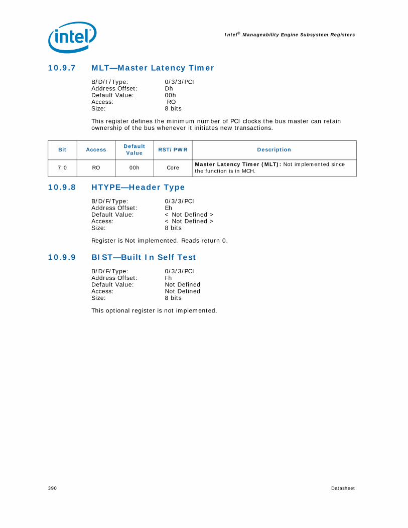
Intel® Manageability Engine Subsystem Registers
390 Datasheet
10.9.7 MLT—Master Latency Timer
B/D/F/Type: 0/3/3/PCIAddress Offset: DhDefault Value: 00hAccess: ROSize: 8 bits
This register defines the minimum number of PCI clocks the bus master can retain ownership of the bus whenever it initiates new transactions.
10.9.8 HTYPE—Header Type
B/D/F/Type: 0/3/3/PCIAddress Offset: EhDefault Value: < Not Defined >Access: < Not Defined >Size: 8 bits
Register is Not implemented. Reads return 0.
10.9.9 BIST—Built In Self Test
B/D/F/Type: 0/3/3/PCIAddress Offset: FhDefault Value: Not DefinedAccess: Not DefinedSize: 8 bits
This optional register is not implemented.
Bit AccessDefault Value
RST/PWR Description
7:0 RO 00h CoreMaster Latency Timer (MLT): Not implemented since the function is in MCH.

Datasheet 391
Intel® Manageability Engine Subsystem Registers
10.9.10 KTIBA—KT IO Block Base Address
B/D/F/Type: 0/3/3/PCIAddress Offset: 10-13hDefault Value: 00000001hAccess: RO, R/WSize: 32 bits
Reset: Host system Reset or D3->D0 transition.
Base Address for the 8byte IO space for KT.
10.9.11 KTMBA—KT Memory Block Base Address
B/D/F/Type: 0/3/3/PCIAddress Offset: 14-17hDefault Value: 00000000hAccess: RO, R/WSize: 32 bits
Reset: Host system Reset or D3->D0 transition
Base Address of Memory Mapped space.
Bit AccessDefault Value
RST/PWR Description
31:16 RO 0000h Core Reserved
15:3 R/W 0000h CoreBase Address (BAR): This field provides the base address of the I/O space (8 consecutive I/O locations).
2:1 RO 00b Core Reserved
0 RO 1b CoreResource Type Indicator (RTE): This bit indicates a request for I/O space
Bit AccessDefault Value
RST/PWR Description
31:12 R/W 00000h CoreBase Address (BAR): This field provides the base address for Memory Mapped I,O BAR. Bits 31:12 correspond to address signals 31:12.
11:4 RO 00h Core Reserved
3 RO 0b CorePrefetchable (PF): This bit indicates that this range is not pre-fetchable.
2:1 RO 00b CoreType (TP): This field indicates that this range can be mapped anywhere in 32-bit address space.
0 RO 0b CoreResource Type Indicator (RTE): This bit indicates a request for register memory space.

Intel® Manageability Engine Subsystem Registers
392 Datasheet
10.9.12 RSVD—Reserved
B/D/F/Type: 0/3/3/PCIAddress Offset: 18-1BhDefault Value: 00000000hAccess: ROSize: 32 bits
10.9.13 RSVD—Reserved
B/D/F/Type: 0/3/3/PCIAddress Offset: 1C-1FhDefault Value: 00000000hAccess: ROSize: 32 bits
10.9.14 RSVD—Reserved
B/D/F/Type: 0/3/3/PCIAddress Offset: 20-23hDefault Value: 00000000hAccess: ROSize: 32 bits
10.9.15 RSVD—Reserved
B/D/F/Type: 0/3/3/PCIAddress Offset: 24-28hDefault Value: 0000000000hAccess: ROSize: 40 bitsBIOS Optimal Default 00h
Bit AccessDefault Value
RST/PWR Description
31:0 RO 00000000h Core Reserved
Bit AccessDefault Value
RST/PWR Description
31:0 RO 00000000h Core Reserved
Bit AccessDefault Value
RST/PWR Description
31:0 RO 00000000h Core Reserved
Bit AccessDefault Value
RST/PWR Description
39:32 RO 0h Reserved
31:0 RO 00000000h Core Reserved

Datasheet 393
Intel® Manageability Engine Subsystem Registers
10.9.16 SS—Sub System Identifiers
B/D/F/Type: 0/3/3/PCIAddress Offset: 2C-2FhDefault Value: 00008086hAccess: R/WOSize: 32 bits
Reset: Host system Reset
These registers are used to uniquely identify the add-in card or the subsystem that the device resides within.
10.9.17 EROM—Expansion ROM Base Address
B/D/F/Type: 0/3/3/PCIAddress Offset: 30-33hDefault Value: 00000000hAccess: ROSize: 32 bits
This optional register is not implemented.
10.9.18 CAP—Capabilities Pointer
B/D/F/Type: 0/3/3/PCIAddress Offset: 34hDefault Value: C8hAccess: ROSize: 8 bits
This optional register is used to point to a linked list of new capabilities implemented by the device.
Bit AccessDefault Value
RST/PWR Description
31:16 R/WO 0000h CoreSubsystem ID (SSID): This is written by BIOS. No hardware action taken on this value.
15:0 R/WO 8086h CoreSubsystem Vendor ID (SSVID): This is written by BIOS. No hardware action taken on this value.
Bit AccessDefault Value
RST/PWR Description
31:11 RO 000000h Core Expansion ROM Base Address (ERBAR):
10:1 RO 000h Core Reserved
0 RO 0b Core Enable (EN): Enable expansion ROM Access.
Bit AccessDefault Value
RST/PWR Description
7:0 RO c8h CoreCapability Pointer (CP): This field indicates that the first capability pointer is offset C8h (the power management capability).

Intel® Manageability Engine Subsystem Registers
394 Datasheet
10.9.19 INTR—Interrupt Information
B/D/F/Type: 0/3/3/PCIAddress Offset: 3C-3DhDefault Value: 0200hAccess: R/W, ROSize: 16 bits
Reset: Host System Reset or D3->D0 reset of the function.
See individual Registers below.
10.9.20 MGNT—Minimum Grant
B/D/F/Type: 0/3/3/PCIAddress Offset: 3EhDefault Value: 00hAccess: ROSize: 8 bits
This optional register is not implemented
10.9.21 MLAT—Maximum Latency
B/D/F/Type: 0/3/3/PCIAddress Offset: 3FhDefault Value: 00hAccess: ROSize: 8 bits
This optional register is not implemented.
Bit AccessDefault Value
RST/PWR Description
15:8 RO 02h Core
Interrupt Pin (IPIN): A value of 0x1/0x2/0x3/0x4 indicates that this function implements legacy interrupt on INTA/INTB/INTC/INTD, respectivelyFunction Value INTx(3 KT/Serial Port) 02h INTB
7:0 R/W 00h Core
Interrupt Line (ILINE): The value written in this register tells which input of the system interrupt controller, the device's interrupt pin is connected to. This value is used by the OS and the device driver, and has no affect on the hardware.
Bit AccessDefault Value
RST/PWR Description
7:0 RO 00h Core Reserved
Bit AccessDefault Value
RST/PWR Description
7:0 RO 00h Core Reserved

Datasheet 395
Intel® Manageability Engine Subsystem Registers
10.9.22 PID—PCI Power Management Capability ID
B/D/F/Type: 0/3/3/PCIAddress Offset: C8-C9hDefault Value: D001hAccess: ROSize: 16 bits
See register definitions below.
10.9.23 PC—PCI Power Management Capabilities
B/D/F/Type: 0/3/3/PCIAddress Offset: CA-CBhDefault Value: 0023hAccess: ROSize: 16 bits
This register implements the power management capabilities of the function.
Bit AccessDefault Value
RST/PWR Description
15:8 RO D0h CoreNext Capability (NEXT): A value of D0h points to the MSI capability.
7:0 RO 01h CoreCap ID (CID): This field indicates that this pointer is a PCI power management.
Bit AccessDefault Value
RST/PWR Description
15:11 RO 00000b CorePME Support (PME): This field indicates no PME# in the PT function.
10 RO 0b Core D2 Support (D2S): The D2 state is not Supported
9 RO 0b Core D1 Support (D1S): The D1 state is not supported
8:6 RO 000b CoreAux Current (AUXC): PME# from D3 (cold) state is not supported; therefore, this field is 000b.
5 RO 1b CoreDevice Specific Initialization (DSI): This bit indicates that no device-specific initialization is required.
4 RO 0b Core Reserved
3 RO 0b CorePME Clock (PMEC): This bit indicates that PCI clock is not required to generate PME#
2:0 RO 011b CoreVersion (VS): This field indicates support for the PCI Power Management Specification, Revision 1.2.

Intel® Manageability Engine Subsystem Registers
396 Datasheet
10.9.24 PMCS—PCI Power Management Control and Status
B/D/F/Type: 0/3/3/PCIAddress Offset: CC-CFhDefault Value: 00000000hAccess: RO/V, RO, R/WSize: 32 bitsBIOS Optimal Default 0000h
Reset: Host System Reset or D3->D0 transition
This register implements the PCI PM Control and Status Register to allow PM state transitions and Wake up
Note: NSR bit of this register. All registers (PCI configuration and Device Specific) marked with D3->D0 transition reset will only do so if the NSR bit reads a 0. If this bit is a 1, the D3->D0 transition will not reset the registers.
Bit AccessDefault Value
RST/PWR Description
31:16 RO 0h Reserved
15 RO 0b CorePME Status (PMES): This bit is set when a PME event is to be requested. Not supported
14:9 RO 00h Core Reserved
8 RO 0b Core PME Enable (PMEE): Not Supported
7:4 RO 0h Core Reserved
3 RO/V 0b Core
No Soft Reset (NSR): When set to1, this bit indicates that devices transitioning from D3hot to D0 because of PowerState commands do not perform an internal reset. Configuration Context is preserved. Upon transition from the D3hot to the D0 Initialized state, no additional operating system intervention is required to preserve Configuration Context beyond writing the PowerState bits.When clear to 0, devices do perform an internal reset upon transitioning from D3hot to D0 via software control of the PowerState bits. Configuration Context is lost when performing the soft reset. Upon transition from the D3hot to the D0 state, full re-initialization sequence is needed to return the device to D0 Initialized.Value in this bit is reflects chicken bit in ME-AUX register x13900, bit [6] which is as follows:0 = Device performs internal reset1 = Device does not perform internal reset
2 RO 0b Core Reserved
1:0 R/W 00b Core
Power State (PS): This field is used both to determine the current power state of the PT function and to set a new power state. The values are:00 = D0 state11 = D3HOT stateWhen in the D3HOT state, the controller's configuration space is available, but the I/O and memory spaces are not. Additionally, interrupts are blocked. If software attempts to write a '10' or '01' to these bits, the write will be ignored.

Datasheet 397
Intel® Manageability Engine Subsystem Registers
10.9.25 MID—Message Signaled Interrupt Capability ID
B/D/F/Type: 0/3/3/PCIAddress Offset: D0-D1hDefault Value: 0005hAccess: ROSize: 16 bits
Message Signalled Interrupt is a feature that allows the device/function to generate an interrupt to the host by performing a DWORD memory write to a system specified address with system specified data. This register is used to identify and configure an MSI capable device.
10.9.26 MC—Message Signaled Interrupt Message Control
B/D/F/Type: 0/3/3/PCIAddress Offset: D2-D3hDefault Value: 0080hAccess: RO, R/WSize: 16 bits
Reset: Host System Reset or D3->D0 transition.
This register provides System Software control over MSI.
Bit AccessDefault Value
RST/PWR Description
15:8 RO 00h CoreNext Pointer (NEXT): This value indicates this is the last item in the list.
7:0 RO 05h CoreCapability ID (CID): This field value of Capabilities ID indicates device is capable of generating MSI.
Bit AccessDefault Value
RST/PWR Description
15:8 RO 00h Core Reserved
7 RO 1b Core64 Bit Address Capable (C64): Capable of generating 64-bit and 32-bit messages.
6:4 R/W 000b CoreMultiple Message Enable (MME): These bits are R/W for software compatibility, but only one message is ever sent by the PT function.
3:1 RO 000b CoreMultiple Message Capable (MMC): Only one message is required.
0 R/W 0b CoreMSI Enable (MSIE): If set, MSI is enabled and traditional interrupt pins are not used to generate interrupts.

Intel® Manageability Engine Subsystem Registers
398 Datasheet
10.9.27 MA—Message Signaled Interrupt Message Address
B/D/F/Type: 0/3/3/PCIAddress Offset: D4-D7hDefault Value: 00000000hAccess: RO, R/WSize: 32 bits
Reset: Host system Reset or D3->D0 transition
This register specifies the DWORD aligned address programmed by system software for sending MSI.
10.9.28 MAU—Message Signaled Interrupt Message Upper Address
B/D/F/Type: 0/3/3/PCIAddress Offset: D8-DBhDefault Value: 00000000hAccess: RO, R/WSize: 32 bits
Reset: Host system Reset or D3->D0 transition
Upper 32 bits of the message address for the 64bit address capable device.
10.9.29 MD—Message Signaled Interrupt Message Data
B/D/F/Type: 0/3/3/PCIAddress Offset: DC-DDhDefault Value: 0000hAccess: R/WSize: 16 bits
Reset: Host system Reset or D3->D0 transition
This 16-bit field is programmed by system software if MSI is enabled
Bit AccessDefault Value
RST/PWR Description
31:2 R/W 00000000h CoreAddress (ADDR): Lower 32 bits of the system specified message address, always DWord aligned.
1:0 RO 00b Core Reserved
Bit AccessDefault Value
RST/PWR Description
31:4 RO 0000000h Core Reserved
3:0 R/W 0000b CoreAddress (ADDR): Upper 4 bits of the system specified message address.
Bit AccessDefault Value
RST/PWR Description
15:0 R/W 0000h CoreData (DATA): This MSI data is driven onto the lower word of the data bus of the MSI memory write transaction.

Datasheet 399
Intel® Manageability Engine Subsystem Registers
10.10 KT IO/ Memory Mapped Device Registers
10.10.1 KTRxBR—KT Receive Buffer Register
B/D/F/Type: 0/3/3/KT MM/IOAddress Offset: 0hDefault Value: 00hAccess: RO/VSize: 8 bits
Reset: Host System Reset or D3->D0 transition.
This implements the KT Receiver Data register. Host access to this address, depends on the state of the DLAB bit {KTLCR[7]). It must be "0" to access the KTRxBR.
RxBR:
Host reads this register when FW provides it the receive data in non-FIFO mode. In FIFO mode, host reads to this register translate into a read from ME memory (RBR FIFO).
Table 25. KT IO/ Memory Mapped Device Register Address Map
Address Offset
Register Symbol
Register NameDefault Value
Access
0h KTRxBR KT Receive Buffer Register 00h RO/V
0h KTTHR KT Transmit Holding Register 00h WO
0h KTDLLR KT Divisor Latch LSB Register 00h R/W/V
1h KTIER KT Interrupt Enable register 00h R/W/V, RO/V
1h KTDLMR KT Divisor Latch MSB Register 00h R/W/V
2h KTIIR KT Interrupt Identification register 01h RO
2h KTFCR KT FIFO Control register 00h WO
3h KTLCR KT Line Control register 03h R/W
4h KTMCR KT Modem Control register 00h RO, R/W
5h KTLSR KT Line Status register 00h RO, RO/CR
6h KTMSR KT Modem Status register 00h RO, RO/CR
7h KTSCR KT Scratch register 00h R/W
Bit AccessDefault Value
RST/PWR Description
7:0 RO/V 00h CoreReceiver Buffer Register (RBR): Implements the Data register of the Serial Interface. If the Host does a read, it reads from the Receive Data Buffer.

Intel® Manageability Engine Subsystem Registers
400 Datasheet
10.10.2 KTTHR—KT Transmit Holding Register
B/D/F/Type: 0/3/3/KT MM/IOAddress Offset: 0hDefault Value: 00hAccess: WOSize: 8 bits
Reset: Host System Reset or D3->D0 transition.
This implements the KT Transmit Data register. Host access to this address, depends on the state of the DLAB bit {KTLCR[7]). It must be "0" to access the KTTHR.
THR:
When host wants to transmit data in the non-FIFO mode, it writes to this register. In FIFO mode, writes by host to this address cause the data byte to be written by hardware to ME memory (THR FIFO).
10.10.3 KTDLLR—KT Divisor Latch LSB Register
B/D/F/Type: 0/3/3/KT MM/IOAddress Offset: 0hDefault Value: 00hAccess: R/W/VSize: 8 bits
Reset: Host System Reset or D3->D0 transition.
This register implements the KT DLL register. Host can Read/Write to this register only when the DLAB bit (KTLCR[7]) is 1. When this bit is 0, Host accesses the KTTHR or the KTRBR depending on Read or Write.
This is the standard Serial Port Divisor Latch register. This register is only for software compatibility and does not affect performance of the hardware.
Bit AccessDefault Value
RST/PWR Description
7:0 WO 00h CoreTransmit Holding Register (THR): Implements the Transmit Data register of the Serial Interface. If the Host does a write, it writes to the Transmit Holding Register.
Bit AccessDefault Value
RST/PWR Description
7:0 R/W/V 00h CoreDivisor Latch LSB (DLL): Implements the DLL register of the Serial Interface.

Datasheet 401
Intel® Manageability Engine Subsystem Registers
10.10.4 KTIER—KT Interrupt Enable Register
B/D/F/Type: 0/3/3/KT MM/IOAddress Offset: 1hDefault Value: 00hAccess: R/W/V, RO/VSize: 8 bits
Reset: Host System Reset or D3 -> D0 transition
This implements the KT Interrupt Enable register. Host access to this address, depends on the state of the DLAB bit {KTLCR[7]). It must be "0" to access this register. The bits enable specific events to interrupt the Host.
10.10.5 KTDLMR—KT Divisor Latch MSB Register
B/D/F/Type: 0/3/3/KT MM/IOAddress Offset: 1hDefault Value: 00hAccess: R/W/VSize: 8 bits
Reset: Host System Reset or D3->D0 transition.
Host can Read/Write to this register only when the DLAB bit (KTLCR[7]) is 1. When this bit is 0, Host accesses the KTIER.
This is the standard Serial interface's Divisor Latch register's MSB. This register is only for SW compatibility and does not affect performance of the hardware.
Bit AccessDefault Value
RST/PWR Description
7:4 RO/V 0h Core Reserved
3 R/W/V 0b CoreMSR (IER2): When set, this bit enables bits in the Modem Status register to cause an interrupt to the host.
2 R/W/V 0b CoreLSR (IER1): When set, this bit enables bits in the Receiver Line Status Register to cause an Interrupt to the Host.
1 R/W/V 0b CoreTHR (IER1): When set, this bit enables an interrupt to be sent to the Host when the transmit Holding register is empty.
0 R/W/V 0b CoreDR (IER0): When set, the Received Data Ready (or Receive FIFO Timeout) interrupts are enabled to be sent to Host.
Bit AccessDefault Value
RST/PWR Description
7:0 R/W/V 00h CoreDivisor Latch MSB (DLM): Implements the Divisor Latch MSB register of the Serial Interface.

Intel® Manageability Engine Subsystem Registers
402 Datasheet
10.10.6 KTIIR—KT Interrupt Identification Register
B/D/F/Type: 0/3/3/KT MM/IOAddress Offset: 2hDefault Value: 01hAccess: ROSize: 8 bits
Reset: See specific Bit descriptions.
The KT IIR register prioritizes the interrupts from the function into 4 levels and records them in the IIR_STAT field of the register. When Host accesses the IIR, hardware freezes all interrupts and provides the priority to the Host. Hardware continues to monitor the interrupts but does not change its current indication until the Host read is over. Table in the Host Interrupt Generation section shows the contents.
Bit AccessDefault Value
RST/PWR Description
7 RO 0b CoreFIFO Enable (FIEN1): This bit is connected by hardware to bit 0 in the FCR register.Reset: Host System Reset or D3->D0 transition.
6 RO 0b CoreFIFO Enable (FIEN0): This bit is connected by hardware to bit 0 in the FCR register.Reset: Host System Reset or D3->D0 transition.
5:4 RO 00b Core Reserved
3:1 RO 000b Core
IIR STATUS (IIRSTS): These bits are asserted by the hardware according to the source of the interrupt and the priority level. Reset: ME system Reset.
0 RO 1b Core
Interrupt Status (INTSTS):0 = Pending interrupt to Host1 = No pending interrupt to Host
Reset: Host system Reset or D3->D0 transition

Datasheet 403
Intel® Manageability Engine Subsystem Registers
10.10.7 KTFCR—KT FIFO Control Register
B/D/F/Type: 0/3/3/KT MM/IOAddress Offset: 2hDefault Value: 00hAccess: WOSize: 8 bits
Reset: Host System Reset or D3->D0 transition
When Host writes to this address, it writes to the KTFCR. The FIFO control Register of the serial interface is used to enable the FIFOs, set the receiver FIFO trigger level and clear FIFOs under the direction of the Host.
When Host reads from this address, it reads the KTIIR.
Bit AccessDefault Value
RST/PWR Description
7:6 WO 00b Core
Receiver Trigger Level (RTL): Trigger level in bytes for the RCV FIFO. Once the trigger level number of bytes is reached, an interrupt is sent to the Host. 00 = 0101 = 0410 = 0811 = 14
5:4 WO 00b Core Reserved
3 WO 0b CoreRDY Mode (RDYM): This bit has no affect on hardware performance.
2 WO 0b CoreXMT FIFO Clear (XFIC): When the Host writes one to this bit, the hardware will clear the XMT FIFO. This bit is self-cleared by hardware.
1 WO 0b CoreRCV FIFO Clear (RFIC): When the Host writes one to this bit, the hardware will clear the RCV FIFO. This bit is self-cleared by hardware.
0 WO 0b CoreFIFO Enable (FIE): When set, this bit indicates that the KT interface is working in FIFO node. When this bit value is changed the RCV and XMT FIFO are cleared by hardware.

Intel® Manageability Engine Subsystem Registers
404 Datasheet
10.10.8 KTLCR—KT Line Control Register
B/D/F/Type: 0/3/3/KT MM/IOAddress Offset: 3hDefault Value: 03hAccess: R/WSize: 8 bits
Reset: Host System Reset or D3->D0 transition.
The line control register specifies the format of the asynchronous data communications exchange and sets the DLAB bit. Most bits in this register have no affect on hardware and are only used by the FW.
Bit AccessDefault Value
RST/PWR Description
7 R/W 0b Core
Divisor Latch Address Bit (DLAB): This bit is set when the Host wants to read/write the Divisor Latch LSB and MSB Registers. This bit is cleared when the Host wants to access the Receive Buffer Register or the Transmit Holding Register or the Interrupt Enable Register.
6 R/W 0b Core Break Control (BC): This bit has no affect on hardware.
5:4 R/W 00b CoreParity Bit Mode (PBM): This bit has no affect on hardware.
3 R/W 0b Core Parity Enable (PE): This bit has no affect on hardware.
2 R/W 0b CoreStop Bit Select (SBS): This bit has no affect on hardware.
1:0 R/W 11b CoreWord Select Byte (WSB): This bit has no affect on hardware.

Datasheet 405
Intel® Manageability Engine Subsystem Registers
10.10.9 KTMCR—KT Modem Control Register
B/D/F/Type: 0/3/3/KT MM/IOAddress Offset: 4hDefault Value: 00hAccess: RO, R/WSize: 8 bits
Reset: Host system Reset or D3->D0 transition.
The Modem Control Register controls the interface with the modem. Since the FW emulates the modem, the Host communicates to the FW via this register. Register has impact on hardware when the Loopback mode is on.
Bit AccessDefault Value
RST/PWR Description
7:5 RO 000b Core Reserved
4 R/W 0b Core
Loop Back Mode (LBM): When set by the Host, this bit indicates that the serial port is in loop Back mode. This means that the data that is transmitted by the host should be received. Helps in debug of the interface.
3 R/W 0b CoreOutput 2 (OUT2): This bit has no affect on hardware in normal mode. In loop back mode the value of this bit is written by hardware to the Modem Status Register bit 7.
2 R/W 0b CoreOutput 1 (OUT1): This bit has no affect on hardware in normal mode. In loop back mode the value of this bit is written by hardware to Modem Status Register bit 6.
1 R/W 0b Core
Request to Send Out (RTSO): This bit has no affect on hardware in normal mode. In loopback mode, the value of this bit is written by hardware to Modem Status Register bit 4.
0 R/W 0b Core
Data Terminal Ready Out (DRTO): This bit has no affect on hardware in normal mode. In loopback mode, the value in this bit is written by hardware to Modem Status Register Bit 5.
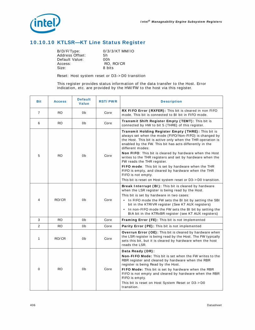
Intel® Manageability Engine Subsystem Registers
406 Datasheet
10.10.10 KTLSR—KT Line Status Register
B/D/F/Type: 0/3/3/KT MM/IOAddress Offset: 5hDefault Value: 00hAccess: RO, RO/CRSize: 8 bits
Reset: Host system reset or D3->D0 transition
This register provides status information of the data transfer to the Host. Error indication, etc. are provided by the HW/FW to the host via this register.
Bit AccessDefault Value
RST/PWR Description
7 RO 0b CoreRX FIFO Error (RXFER): This bit is cleared in non FIFO mode. This bit is connected to BI bit in FIFO mode.
6 RO 0b CoreTransmit Shift Register Empty (TEMT): This bit is connected by HW to bit 5 (THRE) of this register.
5 RO 0b Core
Transmit Holding Register Empty (THRE): This bit is always set when the mode (FIFO/Non-FIFO) is changed by the Host. This bit is active only when the THR operation is enabled by the FW. This bit has acts differently in the different modes:Non FIFO: This bit is cleared by hardware when the Host writes to the THR registers and set by hardware when the FW reads the THR register.FIFO mode: This bit is set by hardware when the THR FIFO is empty, and cleared by hardware when the THR FIFO is not empty.This bit is reset on Host system reset or D3->D0 transition.
4 RO/CR 0b Core
Break Interrupt (BI): This bit is cleared by hardware when the LSR register is being read by the Host.This bit is set by hardware in two cases:• In FIFO mode the FW sets the BI bit by setting the SBI
bit in the KTRIVR register (See KT AUX registers)• In non-FIFO mode the FW sets the BI bit by setting the
BIA bit in the KTRxBR register (see KT AUX registers)
3 RO 0b Core Framing Error (FE): This bit is not implemented
2 RO 0b Core Parity Error (PE): This bit is not implemented
1 RO/CR 0b Core
Overrun Error (OE): This bit is cleared by hardware when the LSR register is being read by the Host. The FW typically sets this bit, but it is cleared by hardware when the host reads the LSR.
0 RO 0b Core
Data Ready (DR):Non-FIFO Mode: This bit is set when the FW writes to the RBR register and cleared by hardware when the RBR register is being Read by the Host.FIFO Mode: This bit is set by hardware when the RBR FIFO is not empty and cleared by hardware when the RBR FIFO is empty.This bit is reset on Host System Reset or D3->D0 transition.

Datasheet 407
Intel® Manageability Engine Subsystem Registers
10.10.11 KTMSR—KT Modem Status Register
B/D/F/Type: 0/3/3/KT MM/IOAddress Offset: 6hDefault Value: 00hAccess: RO, RO/CRSize: 8 bits
Reset: Host system Reset or D3->D0 transition
The functionality of the Modem is emulated by the FW. This register provides the status of the current state of the control lines from the modem.
10.10.12 KTSCR—KT Scratch Register
B/D/F/Type: 0/3/3/KT MM/IOAddress Offset: 7hDefault Value: 00hAccess: R/WSize: 8 bits
Reset: Host system reset or D3->D0 transition
This register has no affect on hardware. This is for the programmer to hold data temporarily.
Bit AccessDefault Value
RST/PWR Description
7 RO 0b CoreData Carrier Detect (DCD): In Loop Back mode this bit is connected by hardware to the value of MCR bit 3.
6 RO 0b CoreRing Indicator (RI): In Loop Back mode this bit is connected by hardware to the value of MCR bit 2.
5 RO 0b CoreData Set Ready (DSR): In Loop Back mode this bit is connected by hardware to the value of MCR bit 0.
4 RO 0b CoreClear To Send (CTS): In Loop Back mode this bit is connected by hardware to the value of MCR bit 1.
3 RO/CR 0b CoreDelta Data Carrier Detect (DDCD): This bit is set when bit 7 is changed. This bit is cleared by hardware when the MSR register is being read by the HOST driver.
2 RO/CR 0b Core
Trailing Edge of Read Detector (TERI): This bit is set when bit 6 is changed from 1 to 0. This bit is cleared by hardware when the MSR register is being read by the Host driver.
1 RO/CR 0b CoreDelta Data Set Ready (DDSR): This bit is set when bit 5 is changed. This bit is cleared by hardware when the MSR register is being read by the Host driver.
0 RO/CR 0b CoreDelta Clear To Send (DCTS): This bit is set when bit 4 is changed. This bit is cleared by hardware when the MSR register is being read by the Host driver.
Bit AccessDefault Value
RST/PWR Description
7:0 R/W 00h Core Scratch Register Data (SCRD):

Intel® Manageability Engine Subsystem Registers
408 Datasheet
§ §

Datasheet 409
Intel® Trusted Execution Technology Registers (Intel® 82Q45 and 82Q43 GMCH Only)
11 Intel® Trusted Execution Technology Registers (Intel® 82Q45 and 82Q43 GMCH Only)
This section covers the Intel® Trusted Execution Technology specific registers implemented in the (G)MCH. For more information on Intel® Trusted Execution Technology enabled platform, refer to the Intel® Trusted Execution Technology BIOS writer’s guide.
11.1 Intel Trusted Execution Technology Specific Registers
Address Offset
Symbol Register Name Srlz Default Value Access
0h TXT.STS TXT Status Register 000010h RO
8h TXT.ESTS TXT Error Status Register 00hRWC, RO
10–17hTXT.THREAD.EXIST
STXT Thread Exists Register
0000000000000000h
RO
20–27h TXT.THREADS.JOIN TXT Threads Join Register000000000000
0000hRO
30–33hTXT.ERRORCODE (AKA TXT.CRASH)
TXT ERRORCODE Register (Also known as TXT CRASH)
00000000h RWC
38–3Fh TXT.CMD.RESET TXT System Reset Command FA N/A WO
48–4FhTXT.CMD.CLOSE-
PRIVATETXT Close Private Command N/A WO
110–117h TXT.DID TXT Device ID Register 8003h RW, RO
258–25Fh TXT.CMD.FLUSH-WB TXT Flush Write Buffer Command FA N/A WO
270–277hTXT.SINIT.MEMORY.
BASETXT SINIT Code Base Register
0000000000000000h
RW, RO
278–27FhTXT.SINIT.MEMORY.
SIZETXT SINIT Memory Size Register
0000000000000000h
RW,
290–297h TXT.MLE.JOIN TXT MLE Join Base Register000000000000
0000hRW, RO
300–307h TXT.HEAP.BASE TXT Heap Base Register000000000000
0000hRW
308–30Fh TXT.HEAP.SIZE TXT Heap Size Register000000000000
0000hRW
310–317h TXT.MSEG.BASE TXT MSEG Base Register000000000000
0000hRW/L

Intel® Trusted Execution Technology Registers (Intel® 82Q45 and 82Q43 GMCH Only)
410 Datasheet
Note: Srlz: Indicates if a serializing step is required by software (for example, a read) before or after a write to the register. Note that this is referring to serializing at the chipset hardware level. Since TXT space is memory-mapped, multiple commands or writes can be enqueued in a back-to-back sequence. If a preceding command or write takes several clocks to be fully processed, the subsequent accesses may be handled incorrectly. Therefore, simply serializing these cycles as they leave the processor may not be sufficient to guarantee that they are appropriately serialized by the time they are processed in the chipset. A read following the write does guarantee that a subsequent write is serialized after the first write. FA=Fence after. FB=Fence before.
318–31Fh TXT.MSEG.SIZE TXT MSEG Size Address Register000000000000
0000hRW/L
320–327h TXT.SCRATCHPAD.0 TXT Scratch Pad 0 Register000000000000
0000hRW
328–32Fh TXT.SCRATCHPAD.1 TXT Scratch Pad 1 Register000000000000
0000hRW
330–337h TXT.DPR DMA Protected Range000000000000
0000h
RO, RW/L, RWO
380–387hTXT.CMD.OPEN.LOC
ALITY1TXT Open Locality 1 Command FA N/A WO
388–38FhTXT.CMD.CLOSE.LO
CALITY1TXT Close Locality 1 Command FA N/A WO
390–397hTXT.CMD.OPEN.LOC
ALITY2TXT Open Locality 2 Command FA N/A WO
398–39FhTXT.CMD.CLOSE.LO
CALITY2TXT Close Locality 2 Command FA N/A WO
400–41Fh TXT.PUBLIC.KEY TXT Chipset Public Key Hash
00000000de4498a3619fa4f4e5e30200613d4a51a6f9e712h
RO
8E0–8E7h TXT.CMD.SECRETS TXT Secrets Command FA N/A WO
8E8–8EFhTXT.CMD.NO-
SECRETSTXT No Secrets Command FA N/A WO
8F0–8F7h TXT.E2STS TXT Extended Error Status Register000000000000
0000hRO
Address Offset
Symbol Register Name Srlz Default Value Access

Datasheet 411
Intel® Trusted Execution Technology Registers (Intel® 82Q45 and 82Q43 GMCH Only)
11.1.1 TXT.STS—TXT Status Register
B/D/F/Type: 0/0/0/TXT SpecificAddress Offset: 0-2hDefault Value: 000010hAccess: ROSize: 24 bitsBIOS Optimal Default 00h
This register is used to read the status of the TXT Command/Status Engine functional block in the chipset.
Bit AccessDefault Value
Description
23:17 RO 0h Reserved
16 RO 0b
TXT.LOCALITY2.OPEN.STS (TXT.LOCALITY2.OPEN.STS): This bit is set when either the TXT.CMD.OPEN.LOCALITY2 command or the TXT.CMD.OPEN.PRIVATE is seen by the chipset. It is cleared on reset or when either TXT.CMD.CLOSE.LOCALITY2 or TXT.CMD.CLOSE.PRIVATE is seen. This bit can be used by SW as a positive indication that the command has taken effect.
15 RO 0b
TXT.LOCALITY1.OPEN.STS (TXT.LOCALITY1.OPEN.STS): This bit is set when the TXT.CMD.OPEN.LOCALITY1 command is seen by the chipset. It is cleared on reset or when TXT.CMD.CLOSE.LOCALITY1 is seen. This bit can be used by SW as a positive indication that the command has taken effect.
14:8 RO 0b Reserved
7 RO 0bTXT Private-Open Status (TXT.PRIVATE-OPEN.STS): This bit will be set to 1 when the TXT Private address is opened. This bit cleared by the TXT.CMD.CLOSE-PRIVATE or by a system reset.
6:5 RO 0b Reserved
4:4 RO 1b Reserved
3:2 RO 0b Reserved
1 RO 0b
SEXIT Done Status (SEXIT.DONE.STS): This bit is set when all of the bits in the TXT.THREADS.JOIN register are clear 0. Thus, this bit will be set immediately after reset (since the bits are all 0). This bit will be cleared on the receipt of the first TXT.CYC.SENTER-ACK. Once all threads have done the TXT.CYC.SEXIT-ACK, the TXT.THREAD.JOIN register will be 0, so the chipset will set this bit.
0 RO 0b
SENTER Done Status (SENTER.DONE.STS): The chipset sets this bit when it sees all of the threads have done the TXT.CYC.SENTER-ACK. When any of the threads does the TXT.CYC.SEXIT-ACK, the TXT.THREADS.JOIN and TXT.THREADS.EXISTS registers will not be equal, so the chipset will clear this bit.

Intel® Trusted Execution Technology Registers (Intel® 82Q45 and 82Q43 GMCH Only)
412 Datasheet
11.1.2 TXT.ESTS—TXT Error Status Register
B/D/F/Type: 0/0/0/TXT SpecificAddress Offset: 8hDefault Value: 00hAccess: RWC, ROSize: 8 bits
This register is used to read the status associated with various errors that might be detected. All defined bits in this register are sticky.
Bit AccessDefault Value
Description
7 RWC 0b Reserved
6 RWC 0b
TXT Wake Error Status (TXT.WAKE-ERROR.STS): The chipset sets this bit when it detects that there might have been secrets in memory and a reset or power failure occurred.If this bit is set after a system reset, the chipset will prevent memory accesses until specifically enabled. The software that is authorized to enable the memory accesses will also be responsible for clearing the secrets from memory.Software can read chipset-specific registers to determine the specific cause of the error. The location of those bits is beyond the scope of this specification.On a reset, if CPU_RESET_DONE_ACK_SECRET is received, then this bit is set to '1'.On a reset, if CPU_RESET_DONE_ACK is received, then this bit is cleared to '0'.Software can clear this bit by writing a '1' to it.This bit must be cleared if a read to 0xFED4_0000 returns a 1 in bit 0.
5:1 RWC 0b Reserved
0 RO 0b
TXT Reset Status (TXT.TXT_RESET.STS): The chipset sets this bit to ‘1’ to indicate that the platform experienced a TXT reset. To maintain TXT integrity, while this bit is set, a TXT measured environment cannot be established; consequently Safer Mode Extension (SMX) instructions GETSEC [ENTERACCS] and GETSEC [SENTER] will fail. See Chapter 6, “Safer Mode Extensions Reference” of Intel® 64 and IA-32 Architectures Software Developer’s Manual, Volume 2B. Reads to the TXT public space and other non-SMX instructions will continue to work. This bit must be cleared to re-enable TXT on the platform. Note: This bit is sticky and will only be cleared on a power cycle.

Datasheet 413
Intel® Trusted Execution Technology Registers (Intel® 82Q45 and 82Q43 GMCH Only)
11.1.3 TXT.THREAD.EXISTS—TXT Thread Exists Register
B/D/F/Type: 0/0/0/TXT SpecificAddress Offset: 10-17hDefault Value: 0000000000000000hAccess: RO Size: 64 bits
This register is used to read which threads are registered as TXT capable
Bit AccessDefault Value
Description
63:32 RO0000000
0h
TXT Threads Exists (Reserved) (TXT.THRDS.EXISTS_R): This bit field indicates the threads on the FSB that have issued a cycle. The bit is set based on any processor cycle initiated by the thread after reset. The GETSEC instruction is expected to be performed after each thread has performed at least one cycle. When the chipset detects the presence of a particular thread, it sets the corresponding bit in this register.This register is locked when SENTER is seen on the FSB. The following bit mapping is used:Bits Usage7:0 CPU #0, threads # 1-415:8 CPU #1, threads # 1-423:16 CPU #2, threads # 1-431:24 CPU #3, threads # 1-463:32 ReservedNOTES:The processor is defined by the Defer ID bits, DID[6:5]. The thread is
defined by ATTR[6:5]. At the moment that defines only 4 processor's and 4 threads. The other bits are reserved for future changes.
31:0 RO0000000
0h
TXT Thread Exists (TXT.THRDS.EXISTS): This bit field indicates the threads on the FSB that have issued a cycle. The bit is set based on any processor cycle initiated by the thread after reset. The GETSEC instruction is expected to be performed after each thread has performed at least one cycle. When the chipset detects the presence of a particular thread, it sets the corresponding bit in this register.This register is locked when SENTER is seen on the FSB.The following bit mapping is used:Bits Usage7:0 CPU #0, threads # 1-415:8 CPU #1, threads # 1-423:16 CPU #2, threads # 1-431:24 CPU #3, threads # 1-463:32 ReservedNOTE: The CPU is defined by the Defer ID bits, DID[6:5]. The thread is defined
by ATTR[6:5]. At the moment that defines only 4 processors and 4 threads. The other bits are reserved for future changes.

Intel® Trusted Execution Technology Registers (Intel® 82Q45 and 82Q43 GMCH Only)
414 Datasheet
11.1.4 TXT.THREADS.JOIN—TXT Threads Join Register
B/D/F/Type: 0/0/0/TXT SpecificAddress Offset: 20-27hDefault Value: 0000000000000000hAccess: RO Size: 64 bits
This register is used to count the threads that have joined the TXT environment.
Bit AccessDefault Value
Description
63:32 RO 00000000h
TXT Threads Join (Reserved) (TXT.THRDS.JOIN_R): This bit field indicates the threads that have issued an SENTER-ACK cycle. Each bit corresponds to a separate thread. When the chipset observes the SENTER-ACK from the thread, it sets the corresponding bit in this register.The format of the bits in this register is the same as in the TXT.THREADS.EXISTS register.The chipset will set the SENTER.DONE.STS bit when the TXT.THREADS.EXISTS and TXT.THREADS.JOIN fields match and at least one bit in the TXT.THREADS.EXISTS register is set.When the chipset observes the SEXIT.ACK cycle, it will clear the corresponding bit in this register. When it has cleared all the bits, it will set SEXIT.DONE.
31:0 RO 00000000h
TXT Threads Join (TXT.THRDS.JOIN): This bit field indicates the threads that have issued an SENTER-ACK cycle. Each bit corresponds to a separate thread. When the chipset observes the SENTER-ACK from the thread, it sets the corresponding bit in this register.The format of the bits in this register is the same as in the TXT.THREADS.EXISTS register.The chipset will set the SENTER.DONE.STS bit when the TXT.THREADS.EXISTS and TXT.THREADS.JOIN fields match and at least one bit in the TXT.THREADS.EXISTS register is set.When the chipset observes the SEXIT.ACK cycle, it will clear the corresponding bit in this register. When it has cleared all the bits, it will set SEXIT.DONE.

Datasheet 415
Intel® Trusted Execution Technology Registers (Intel® 82Q45 and 82Q43 GMCH Only)
11.1.5 TXT.ERRORCODE (AKA TXT.CRASH)—TXT Error Code Register
B/D/F/Type: 0/0/0/TXT SpecificAddress Offset: 30-33hDefault Value: 00000000hAccess: RWSize: 32 bits
When software discovers an error, it can write this scratchpad register. The register is NOT reset by a standard reset, and thus allows diagnostic software (after the reset) to determine why the SENTER sequence failed (by examining various status bits). All defined bits in this register are sticky across soft reboot.
11.1.6 TXT.CMD.RESET—TXT System Reset Command
When this command is invoked, the chipset resets the entire platform. Hardware naturally delays the assertion of reset sufficiently such that any previous writes to ERRORCODE register should have completed. If software wants to guarantee that it is not reliant upon this race, it must read back the ERRORCODE register before writing the System Reset Command.
11.1.7 TXT.CMD.CLOSE-PRIVATE—TXT Close Private Command
The processor that authenticates the SEXIT code does this to prevent the TXT Private address space from being accessed using standard memory read/write cycles.
System Software (i.e. MLE - Measured Launched Environment) is required to fence after this command is performed. This can be achieved by reading back the STS flag to see that it is no longer set after performing the CLOSE-PRIVATE command.
Bit Access Default Value Description
31:0 RWC 00000000hError Code (CRASH): Default 0 on power-up. Otherwise, previous value on reset.
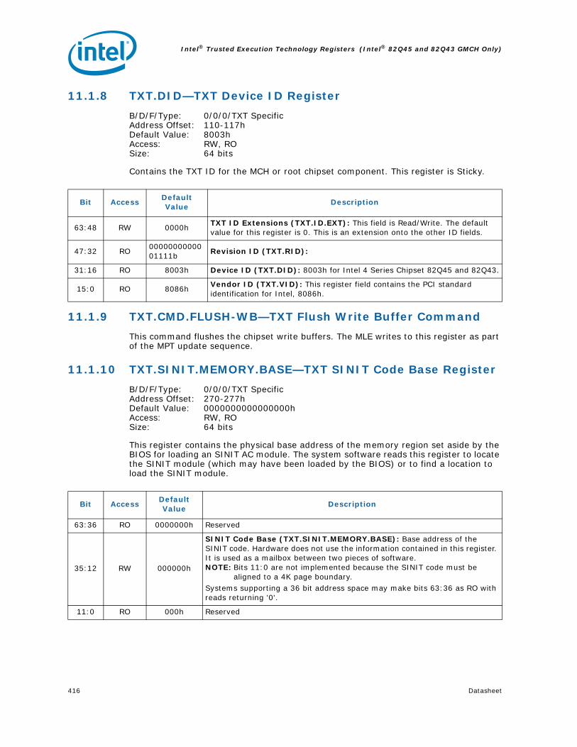
Intel® Trusted Execution Technology Registers (Intel® 82Q45 and 82Q43 GMCH Only)
416 Datasheet
11.1.8 TXT.DID—TXT Device ID Register
B/D/F/Type: 0/0/0/TXT SpecificAddress Offset: 110-117hDefault Value: 8003hAccess: RW, RO Size: 64 bits
Contains the TXT ID for the MCH or root chipset component. This register is Sticky.
11.1.9 TXT.CMD.FLUSH-WB—TXT Flush Write Buffer Command
This command flushes the chipset write buffers. The MLE writes to this register as part of the MPT update sequence.
11.1.10 TXT.SINIT.MEMORY.BASE—TXT SINIT Code Base Register
B/D/F/Type: 0/0/0/TXT SpecificAddress Offset: 270-277hDefault Value: 0000000000000000hAccess: RW, RO Size: 64 bits
This register contains the physical base address of the memory region set aside by the BIOS for loading an SINIT AC module. The system software reads this register to locate the SINIT module (which may have been loaded by the BIOS) or to find a location to load the SINIT module.
Bit AccessDefault Value
Description
63:48 RW 0000hTXT ID Extensions (TXT.ID.EXT): This field is Read/Write. The default value for this register is 0. This is an extension onto the other ID fields.
47:32 RO0000000000001111b
Revision ID (TXT.RID):
31:16 RO 8003h Device ID (TXT.DID): 8003h for Intel 4 Series Chipset 82Q45 and 82Q43.
15:0 RO 8086hVendor ID (TXT.VID): This register field contains the PCI standard identification for Intel, 8086h.
Bit AccessDefault Value
Description
63:36 RO 0000000h Reserved
35:12 RW 000000h
SINIT Code Base (TXT.SINIT.MEMORY.BASE): Base address of the SINIT code. Hardware does not use the information contained in this register. It is used as a mailbox between two pieces of software.NOTE: Bits 11:0 are not implemented because the SINIT code must be
aligned to a 4K page boundary.Systems supporting a 36 bit address space may make bits 63:36 as RO with reads returning '0'.
11:0 RO 000h Reserved

Datasheet 417
Intel® Trusted Execution Technology Registers (Intel® 82Q45 and 82Q43 GMCH Only)
11.1.11 TXT.SINIT.MEMORY.SIZE—TXT SINIT Memory Size Register
B/D/F/Type: 0/0/0/TXT SpecificAddress Offset: 278-27FhDefault Value: 0000000000000000hAccess: RW Size: 64 bits
This register contains the size in bytes of the memory region set aside by the BIOS for loading an SINIT AC module. This register is initialized by the BIOS. The system software may read this register when loading an SINIT module.
11.1.12 TXT.MLE.JOIN—TXT MLE Join Base Register
B/D/F/Type: 0/0/0/TXT SpecificAddress Offset: 290-297hDefault Value: 0000000000000000hAccess: RW, RO Size: 64 bits
Holds a physical address pointer to the base of the join data structure referenced by RLPs in response to a GETSEC[WAKEUP] while operating between SENTER and SEXIT.
Bit AccessDefault Value
Description
63:0 RW0000000000
000000h
TXT.SINIT.SIZE (TXT.SINIT.SIZE): Base address of the SINIT code. Hardware does not use the information contained in this register. It is used as a mailbox between two pieces of software.Note: Bits 11:0 are not implemented because the SINIT code must be aligned to a 4K page boundary.Systems supporting a 36 bit address space may make bits 63:36 as RO with reads returning '0'.
Bit AccessDefault Value
Description
63:36 RO 0000000h
TXT MLE Join Base (Reserved) (TXT.MLE.JOIN_R): Base address of the MLE join code.For chipsets that only support 64GB FSB addressing (36b addressing), bits 63:36 may be RO – reserved(0)
35:0 RW00000000
0h
TXT MLE Join Base (TXT.MLE.JOIN): Base address of the MLE join code.For chipsets that only support 64 GB FSB addressing (36b addressing), bits 63:36 may be RO – reserved(0)

Intel® Trusted Execution Technology Registers (Intel® 82Q45 and 82Q43 GMCH Only)
418 Datasheet
11.1.13 TXT.HEAP.BASE—TXT Heap Base Register
B/D/F/Type: 0/0/0/TXT SpecificAddress Offset: 300-307hDefault Value: 0000000000000000hAccess: RW Size: 64 bits
This register contains the physical base address of the TXT Heap memory region. The BIOS initializes this register. The system software and MLE read this register to locate the TXT Heap.
11.1.14 TXT.HEAP.SIZE—TXT Heap Size Register
B/D/F/Type: 0/0/0/TXT SpecificAddress Offset: 308-30FhDefault Value: 0000000000000000hAccess: RW; Size: 64 bits
This register contains the size in bytes of the TXT Heap memory region. The BIOS initializes this register. The system software and the MLE read this register to determine the TXT Heap size.
11.1.15 TXT.MSEG.BASE—TXT MSEG Base Register
B/D/F/Type: 0/0/0/TXT SpecificAddress Offset: 310-317hDefault Value: 0000000000000000hAccess: RW/L Size: 64 bits
This register provides the base address of MSEG. This register is locked by SMM D_LCK and when locked neither public nor private writes can change its value.
Bit AccessDefault Value
Description
63:0 RW0000000000000000h
Heap Base Address (TXT.HEAP.BASE): Base address of the Heap. Systems must implement all 64 bits as RW.
Bit AccessDefault Value
Description
63:0 RW0000000000000000h
Heap Size (TXT.HEAP.SIZE): Size of the total Device space in bytes
Bit AccessDefault Value
Description
63:0 RW/L0000000000000000h
MSEG Base Address (MSEG.BASE): BIOS writes the base of MSEG into this register.

Datasheet 419
Intel® Trusted Execution Technology Registers (Intel® 82Q45 and 82Q43 GMCH Only)
11.1.16 TXT.MSEG.SIZE—TXT MSEG Size Address Register
B/D/F/Type: 0/0/0/TXT SpecificAddress Offset: 318-31FhDefault Value: 0000000000000000hAccess: RW/L Size: 64 bits
This register provides the size of MSEG. This register is locked by SMM D_LCK and when locked neither public nor private writes can change its value.
11.1.17 TXT.SCRATCHPAD.0—TXT Scratch Pad 0 Register
B/D/F/Type: 0/0/0/TXT SpecificAddress Offset: 320-327hDefault Value: 0000000000000000hAccess: RW Size: 64 bits
Scratchpad register 0
11.1.18 TXT.SCRATCHPAD.1—TXT Scratch Pad 1 Register
B/D/F/Type: 0/0/0/TXT SpecificAddress Offset: 328-32FhDefault Value: 0000000000000000hAccess: RW Size: 64 bits
Scratchpad register 1
Bit AccessDefault Value
Description
63:0 RW/L0000000000
000000hMSEG Size Value (MSEG.SIZE): This is the size of the MSEG region in bytes.
Bit AccessDefault Value
Description
63:0 RW0000000000
000000hScratch Pad 0 (SCRATCH0): General Scratch Pad 0
Bit AccessDefault Value
Description
63:0 RW0000000000
000000hScratch Pad 1 (SCRATCH1): General Scratch Pad 1

Intel® Trusted Execution Technology Registers (Intel® 82Q45 and 82Q43 GMCH Only)
420 Datasheet
11.1.19 TXT.DPR—DMA Protected Range
B/D/F/Type: 0/0/0/TXT SpecificAddress Offset: 330-337hDefault Value: 0000000000000000hAccess: RO, RW/L, RWO Size: 64 bits
DMA protected range register.
11.1.20 TXT.CMD.OPEN.LOCALITY1—TXT Open Locality 1 Command
This command will open Locality1 for decode as an TXT space by the chipset. If the locality is closed, then cycles to the locality 1 address range are not decoded as TXT cycles.
Note: PRIVATE space must also be Open for Locality 1 to be decoded as TXT Space.
Bit AccessDefault Value
Description
63:32 RO 00000000h Reserved
31:20 RO 000hTop of DPR (TopOfDPR): Top address + 1 of DPR. This is the base of TSEG. Bits 19:0 of the BASE reported here are 0x0_0000.
19:12 RO 00h Reserved
11:4 RW/L 00h
DMA Protected Memory Size (DPR.SIZE): This is the size of memory, in MB, that will be protected from DMA accesses. A value of 0x00 in this field means no additional memory is protected. The maximum amount of memory that will be protected is 255 MB. The amount of memory reported in this field will be protected from all DMA accesses, including translated CPU accesses and graphics. The top of the protected range is the BASE of TSEG–1.
NOTE: If TSEG is not enabled, then the top of this range becomes the base of stolen graphics, or ME stolen space or TOLUD, whichever would have been the location of TSEG, assuming it had been enabled.
The DPR range works independently of any other range, including the PMRC checks in VTd, and is done post any VTd translation. Therefore, incoming cycles are checked against this range after the VTd translation and faulted if they hit this protected range, even if they passed the VTd translation. All the memory checks are OR'ed with respect to NOT being allowed to go to memory. So if either PMRC, DPR OR a VTd translation disallows the cycle, then the cycle is not allowed to go to memory. Or in other words, all the above checks must pass before a cycle is allowed to DRAM.
3:1 RO 000b Reserved
0 RWO 0b LOCK (LOCK): Bits 19:0 are locked down in this register when this bit is set.
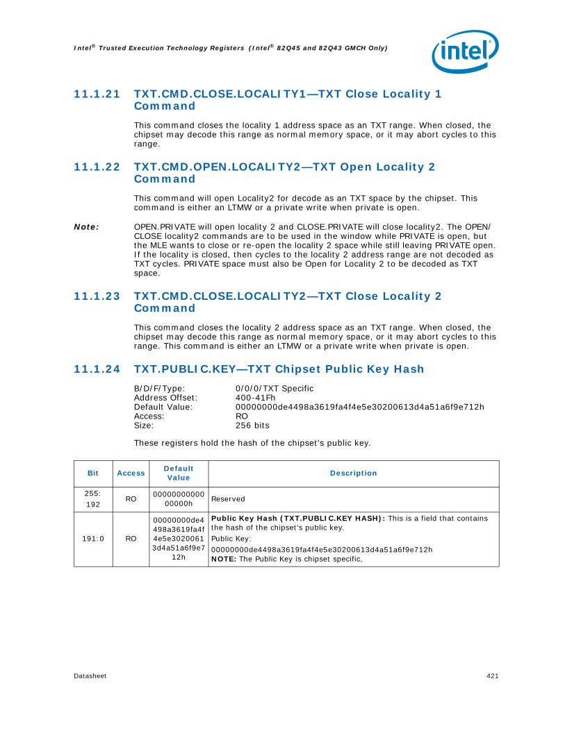
Datasheet 421
Intel® Trusted Execution Technology Registers (Intel® 82Q45 and 82Q43 GMCH Only)
11.1.21 TXT.CMD.CLOSE.LOCALITY1—TXT Close Locality 1 Command
This command closes the locality 1 address space as an TXT range. When closed, the chipset may decode this range as normal memory space, or it may abort cycles to this range.
11.1.22 TXT.CMD.OPEN.LOCALITY2—TXT Open Locality 2 Command
This command will open Locality2 for decode as an TXT space by the chipset. This command is either an LTMW or a private write when private is open.
Note: OPEN.PRIVATE will open locality 2 and CLOSE.PRIVATE will close locality2. The OPEN/CLOSE locality2 commands are to be used in the window while PRIVATE is open, but the MLE wants to close or re-open the locality 2 space while still leaving PRIVATE open. If the locality is closed, then cycles to the locality 2 address range are not decoded as TXT cycles. PRIVATE space must also be Open for Locality 2 to be decoded as TXT space.
11.1.23 TXT.CMD.CLOSE.LOCALITY2—TXT Close Locality 2 Command
This command closes the locality 2 address space as an TXT range. When closed, the chipset may decode this range as normal memory space, or it may abort cycles to this range. This command is either an LTMW or a private write when private is open.
11.1.24 TXT.PUBLIC.KEY—TXT Chipset Public Key Hash
B/D/F/Type: 0/0/0/TXT SpecificAddress Offset: 400-41FhDefault Value: 00000000de4498a3619fa4f4e5e30200613d4a51a6f9e712hAccess: RO Size: 256 bits
These registers hold the hash of the chipset's public key.
Bit AccessDefault Value
Description
255:192
RO00000000000
00000hReserved
191:0 RO
00000000de4498a3619fa4f4e5e30200613d4a51a6f9e7
12h
Public Key Hash (TXT.PUBLIC.KEY HASH): This is a field that contains the hash of the chipset's public key. Public Key:00000000de4498a3619fa4f4e5e30200613d4a51a6f9e712hNOTE: The Public Key is chipset specific,

Intel® Trusted Execution Technology Registers (Intel® 82Q45 and 82Q43 GMCH Only)
422 Datasheet
11.1.25 TXT.CMD.SECRETS—TXT Secrets Command
The ILP SINIT code does this to tell the chipset that there are going to be secrets in memory. This is used when determining whether to block memory after a reset or power failure.
11.1.26 TXT.CMD.NO-SECRETS—TXT Secrets Command
The CPU that authenticates the SEXIT code does this to tell the chipset that there are no more secrets in memory. It is also used by the Authenticated Code that wipes secrets from memory after a reset.
11.1.27 TXT.E2STS—TXT Extended Error Status Register
B/D/F/Type: 0/0/0/TXT SpecificAddress Offset: 8F0-8F7hDefault Value: 0000000000000000hAccess: RO Size: 64 bits
This register is used to read the status associated with various errors that might be detected. The bits in this register are only valid if the TXT.WAKE-ERROR.STS bit is set in the TXT.ESTS register. The bits in this register are all sticky. The default value is undefined.
Bit AccessDefault Value
Description
63:33 RO 0h Reserved
32 RO 0b
TXT Reset Policy (TXT.RESET.POLICY): When cleared to '0', an assertion of the TXTRESET# pin will cause a full system reset, whereby the ICH does a handshake with the MCH before asserting the Platform Reset. When set to '1', the ICH will do a power cycle of the platform on an assertion of TXTRESET#. Default=0.
31:3 RO 0b Reserved
2 RO 0bTXT Memory Block Status (TXT.BLOCK-MEM.STS): This bit indicates if the ICH has indicated to the MCH that it should block memory accesses. Reset only by RTEST#.
1 RO 0bTXT Secrets Status (TXT.SECRETS.STS): This bit indicates if there are any potential secrets in memory. This is used in the setting of the various flags. Reset only by RTEST#.
0 RO 0bTXT Sleep entry error status (TXT.SLP-ENTRY-ERROR.STS): This bit indicates if there has been an improper attempt to go to sleeping state.Reset only by RTEST#.

Datasheet 423
Intel® Trusted Execution Technology Registers (Intel® 82Q45 and 82Q43 GMCH Only)
11.2 Intel® TXT Memory Map
Intel TXT introduces a new memory configuration space and requires physical memory be allocated from the physical memory map. The Intel TXT configuration space is located just below the top of the 4 GB addressable space. The Intel TXT device memory is allocated from the top of the physical memory below 4 GB and must be allocated below other chipset memory regions. Both the Intel TXT configuration space and Intel TXT device memory must be reported as unavailable to the operating system.
11.2.1 Intel® TXT Private Space
The Intel TXT private configuration space is decoded beginning at the fixed address FED20000h and is only accessible by the AC modules and MLE. Special TXT.RD and TXT.WT cycles have been defined to access this space. Intel TXT management registers are located in this space and are used by the authenticated code modules and the MLE to launch and maintain the Intel TXT environment. Any attempt by the BIOS to read Intel TXT private space will return invalid data. BIOS must report this region as unavailable to the OS.
11.2.2 Intel® TXT Public Space
The Intel TXT public configuration space is decoded beginning at the fixed address FED30000h. The registers located in the Intel TXT public space can be accessed using standard memory reads and writes. General purpose Intel TXT configuration registers are located in this space and the BIOS must report this region as unavailable to the OS.
11.2.3 TPM Decode Area
The TPM decode area provides access to TPM configuration registers and is decoded beginning at the fixed address FED40000h. This space is divided into multiple 4K pages, also known as localities, with each page controlled by a different set of attributes. The pages may be accessed by Intel TXT cycles only or Intel TXT cycles and Private cycles, or Intel TXT cycles, Private cycles, and Public cycles. See the TPM PC Client specifications for details regarding the TPM configuration space.
§ §

Intel® Trusted Execution Technology Registers (Intel® 82Q45 and 82Q43 GMCH Only)
424 Datasheet

Datasheet 425
Intel® Virtualization Technology for Directed I/O Registers (D0:F0) (Intel® 82Q45 GMCH Only)
12 Intel® Virtualization Technology for Directed I/O Registers (D0:F0) (Intel® 82Q45 GMCH Only)
12.1 DMI and PEG VC0/VCp Remap Registers
Table 26. Intel® Virtualization Technology For Directed I/O Register Address Map
Address Offset
Register Symbol
Register NameDefault Value
Access
0–3h VER_REG Version Register 00000010h RO
8–Fh CAP_REG Capability Register00C9008020
630272h RO
10–17h ECAP_REG Extended Capability Register00000000000
01000h RO
18–1Bh GCMD_REG Global Command Register 00000000h RO, W
1C–1Fh GSTS_REG Global Status Register 00000000h RO
20–27h RTADDR_REG Root-Entry Table Address Register00000000000
00000h R/W, RO
28–2Fh CCMD_REG Context Command Register00000000000
00000h W, R/W, RO
34–37h FSTS_REG Fault Status Register 00000000h RO, RO/P, R/WC/P
38–3Bh FECTL_REG Fault Event Control Register 80000000h R/W, RO
3C–3Fh FEDATA_REG Fault Event Data Register 00000000h RO, R/W
40–43h FEADDR_REG Fault Event Address Register 00000000h RO, R/W
44–47h FEUADDR_REG Fault Event Upper Address Register 00000000h RO
58–5Fh AFLOG_REG Advanced Fault Log Register00000000000
00000h RO
64–67h PMEN_REG Protected Memory Enable Register 00000000h RO, R/W
68–6Bh PLMBASE_REG Protected Low-Memory Base Register 00000000h R/W, RO
6C–6Fh PLMLIMIT_REG Protected Low-Memory Limit Register 00000000h R/W, RO
70–77h PHMBASE_REG Protected High-Memory Base Register00000000000
00000h RO, R/W
78–7FhPHMLIMIT_RE
GProtected High-Memory Limit Register
0000000000000000h
R/W, RO
100–107h IVA_REG Invalidate Address Register00000000000
00000h W, RO

Intel® Virtualization Technology for Directed I/O Registers (D0:F0) (Intel® 82Q45 GMCH Only)
426 Datasheet
12.1.1 VER_REG—Version Register
B/D/F/Type: 0/0/0/VC0PREMAPAddress Offset: 0-3hDefault Value: 00000010hAccess: ROSize: 32 bits
This register reports the architecture version supported. Backward compatibility for the architecture is maintained with new revision numbers, allowing software to load DMA-remapping drivers written for prior architecture versions.
12.1.2 CAP_REG—Capability Register
B/D/F/Type: 0/0/0/VC0PREMAPAddress Offset: 8-FhDefault Value: 00C9008020630272hAccess: ROSize: 64 bits
This register reports general DMA remapping hardware capabilities.
Bit AccessDefault Value
RST/PWR Description
31:8 RO000000000000000000000000b
Core Reserved
7:4 RO 0001b CoreMajor Version number (MAX): This field indicates supported architecture version.
3:0 RO 0000b CoreMinor Version number (MIN): This field indicates supported architecture minor version.
Bit AccessDefault Value
RST/PWR Description
63:56 RO 00h Core Reserved
55 RO 1b Core
DMA Read Draining (DRD):0 = On IOTLB invalidations, hardware does not support
draining of translated DMA read requests queued within the root complex.
1 = On IOTLB invalidations, hardware supports draining of translated DMA read requests queued within the root complex.
Indicates supported architecture version.
54 RO 1b Core
DMA Write Draining (DWD):0 = On IOTLB invalidations, hardware does not support
draining of translated DMA writes queued within the root complex.
1 = On IOTLB invalidations, hardware supports draining of translated DMA writes queued within the root complex.
53:48 RO 001001b Core
Maximum Address Mask Value (MAMV): The value in this field indicates the maximum supported value for the Address Mask (AM) field in the Invalidation Address (IVA_REG) register.

Datasheet 427
Intel® Virtualization Technology for Directed I/O Registers (D0:F0) (Intel® 82Q45 GMCH Only)
47:40 RO 00000000b Core
Number of Faultrecording Registers (NFR): This field indicates a value of N-1, where N is the number of fault recording registers supported by hardware.Implementations must support at least one fault recording register (NFR = 0) for each DMAremapping hardware unit in the platform.The maximum number of fault recording registers per DMA-remapping hardware unit is 256.Bit 40 in the capability register is the least significant bit of the NFR field (47:40).
39 RO 1b Core
Page Selective Invalidation Support (PSI): 0 = DMAr engine does not support page selective
invalidations1 = DMAr engine does support page-selective IOTLB
invalidations. The MAMV field indicates the maximum number of contiguous translations that may be invalidated in a single request.
38 RO 0b Core Reserved
37:34 RO 0000b Core
Super Page Support (SPS): This field indicates the super page sizes supported by hardware. A value of 1 in any of these bits indicates the corresponding super-page size is supported. The super-page sizes corresponding to various bit positions within this field are:0 = 21-bit offset to page frame1 = 30-bit offset to page frame2 = 39-bit offset to page frame3 = 48-bit offset to page frame
33:24 RO 020h Core
Fault-recording Register offset (FRO): This field specifies the location to the first fault recording register relative to the register base address of this DMA-remapping hardware unit. If the register base address is X, and the value reported in this field is Y, the address for the first fault recording register is calculated as X+(16*Y).
23 RO 0b Core
Isochrony (Isoch): 0 = DMA-remapping hardware unit has no critical
isochronous requesters in its scope.1 = DMA-remapping hardware unit has one or more critical
isochronous requesters in its scope. To ensure isochronous performance, software must ensure invalidation operations do not impact active DMA streams. This implies that when DMA is active, software perform page-selective invalidations (instead of coarser invalidations).
22 RO 1b Core
Zero Length Read (ZLR): 0 = Remapping hardware unit blocks (and treats as fault)
zero length DMA read requests to write-only pages.1 = Remapping hardware unit supports zero length DMA
read requests to write-only pages.
Bit AccessDefault Value
RST/PWR Description

Intel® Virtualization Technology for Directed I/O Registers (D0:F0) (Intel® 82Q45 GMCH Only)
428 Datasheet
21:16 RO 100011b Core
Maximum Guest Address Width (MGAW): This field indicates the maximum DMA virtual addressability supported by remapping hardware.The Maximum Guest Address Width (MGAW) is computed as (N+1), where N is the value reported in this field. For example, a hardware implementation supporting 48-bit MGAW reports a value of 47 (101111b) in this field.If the value in this field is X, DMA requests to addresses above 2(x+1)–1 are always blocked by hardware.Guest addressability for a given DMA request is limited to the minimum of the value reported through this field and the adjusted guest address width of the corresponding page-table structure. (Adjusted guest address widths supported by hardware are reported through the SAGAW field).
15:13 RO 000b Core Reserved
12:8 RO 00010b Core
Supported Adjusted Guest Address Widths (SAGAW): This 5-bit field indicates the supported adjusted guest address widths (which in turn represents the levels of page-table walks) supported by the hardware implementation.A value of 1 in any of these bits indicates the corresponding adjusted guest address width is supported. The adjusted guest address widths corresponding to various bit positions within this field are:0 = 30-bit AGAW (2-level page table)1 = 39-bit AGAW (3-level page table)2 = 48-bit AGAW (4-level page table)3 = 57-bit AGAW (5-level page table)4 = 64-bit AGAW (6-level page table)Software must ensure that the adjusted guest address width used to setup the page tables is one of the supported guest address widths reported in this field.
7 RO 0b Core
Caching Mode (CM): 0 = Hardware does not cache not present and erroneous
entries in the context-cache and IOTLB. Invalidations are not required for modifications to individual not present or invalid entries. However, any modifications that result in decreasing the effective permissions or partial permission increases require invalidations for them to be effective.
1 = Hardware may cache not present and erroneous mappings in the context-cache or IOTLB. Any software updates to the DMA-remapping structures (including updates to not-present or erroneous entries) require explicit invalidation.
Hardware implementations are recommended to support operation corresponding to CM=0.
Bit AccessDefault Value
RST/PWR Description

Datasheet 429
Intel® Virtualization Technology for Directed I/O Registers (D0:F0) (Intel® 82Q45 GMCH Only)
6 RO 1b Core
Protected High-Memory Region (PHMR): 0 = Indicates protected high-memory region not
supported.1 = Indicates protected high-memory region is supported.DMA-remapping hardware implementations on Intel TXT platforms supporting main memory above 4 GB are required to support protected high-memory region.
5 RO 1b Core
Protected Low-Memory Region (PLMR): 0 = Indicates protected low-memory region not supported.1 = Indicates protected low-memory region is supported.DMA-remapping hardware implementations on Intel TXT platforms are required to support protected low-memory region.
4 RO 1b Core
Required Write-Buffer Flushing (RWBF): 0 = Indicates no write-buffer flushing needed to ensure
changes to memory-resident structures are visible to hardware.
1 = Indicates software must explicitly flush the write buffers (through the Global Command register) to ensure updates made to memory-resident DMA-remapping structures are visible to hardware.
3 RO 0b Core
Advanced Fault Logging (AFL): 0 = Indicates advanced fault logging not supported. Only
primary fault logging is supported.1 = Indicates advanced fault logging is supported.
2:0 RO 010b Core
Number of domains supported (ND): 000 =Hardware supports 4-bit domain-IDs with support
for up to 16 domains.001 =Hardware supports 6-bit domain-IDs with support
for up to 64 domains.010 =Hardware supports 8-bit domain-IDs with support
for up to 256 domains.011 =Hardware supports 10-bit domain-IDs with support
for up to 1024 domains.100 =Hardware supports 12-bit domain-IDs with support
for up to 4 KB domains.100 =Hardware supports 14-bit domain-IDs with support
for up to 16 KB domains.110 =Hardware supports 16-bit domain-IDs with support
for up to 64 KB domains.111 =Reserved.
Bit AccessDefault Value
RST/PWR Description

Intel® Virtualization Technology for Directed I/O Registers (D0:F0) (Intel® 82Q45 GMCH Only)
430 Datasheet
12.1.3 ECAP_REG—Extended Capability Register
B/D/F/Type: 0/0/0/VC0PREMAPAddress Offset: 10-17hDefault Value: 0000000000001000hAccess: ROSize: 64 bits
This register reports DMA-remapping hardware extended capabilities
Bit AccessDefault Value
RST/PWR Description
63:24 RO 0s Core Reserved
23:20 RO 0000b Core
Maximum Handle Mask Value (MHMV): The value in this field indicates the maximum supported value for the Handle Mask (HM) field in the interrupt entry cache invalidation descriptor (iec_inv_dsc).This field is valid only when the IR field is reported as Set.
19:18 RO 00b Core Reserved
17:8 RO 010h Core
Invalidation Unit Offset (IVO): This field specifies the location to the first IOTLB invalidation unit relative to the register base address of this DMA-remapping hardware unit.If the register base address is X, and the value reported in this field is Y, the address for the first IOTLB invalidation unit is calculated as X+(16*Y).If N is the value reported in NIU field, the address for the last IOTLB invalidation unit is calculated as X+(16*Y)+(16*N).
7 RO 0b Core
Snoop Control (SC):0 = Hardware does not support 1-setting of the SNP field
in the page-table entries.1 = Hardware supports the 1-setting of the SNP field in the
page-table entries.
6 RO 0b Core
Pass Through (PT):0 = Hardware does not support passthrough translation
type in context entries.1 = Hardware supports pass-through translation type in
context entries.
5 RO 0b Core
Caching Hints (CH):0 = Hardware does not support IOTLB caching hints (ALH
and EH fields in context-entries are treated as reserved).
1 = Hardware supports IOLTB caching hints through the ALH and EH fields in context-entries.
4 RO 0b Core
Extended Interrupt Mode (EIM):0 = Hardware supports only 8-bit APICIDs (Legacy
Interrupt Mode) on Intel®64 and IA-32 platforms and 16- bit APIC-IDs on Itanium™ platforms.
1 = Hardware supports Extended Interrupt Mode (32-bit APIC-IDs) on Intel®64 platforms.
This field is valid only when the IR field is reported as Set.

Datasheet 431
Intel® Virtualization Technology for Directed I/O Registers (D0:F0) (Intel® 82Q45 GMCH Only)
3 RO 0b Core
Interrupt Remapping Support (IR):0 = Hardware does not support interrupt remapping.1 = Hardware supports interrupt remapping.Implementations reporting this field as Set must also support Queued Invalidation (QI = 1b).
2 RO 0b Core
Device IOTLB Support (DI):0 = • 0: Hardware does not support device- IOTLBs.1 = • 1: Hardware supports Device-IOTLBs.Implementations reporting this field as Set must also support Queued Invalidation (QI = 1b).
1 RO 0b CoreQueued Invalidation Support (QI):0 = Hardware does not support queued invalidations.1 = Hardware supports queued invalidations.
0 RO 0b Core
Coherency (C):0 = Hardware accesses to the root, context, and page
table structures are non-coherent (non-snoop)1 = Hardware accesses to the root, context, and page
table structures are coherent (snoop).Hardware writes to the advanced fault log is required to be coherent.
Bit AccessDefault Value
RST/PWR Description

Intel® Virtualization Technology for Directed I/O Registers (D0:F0) (Intel® 82Q45 GMCH Only)
432 Datasheet
12.1.4 GCMD_REG—Global Command Register
B/D/F/Type: 0/0/0/VC0PREMAPAddress Offset: 18-1BhDefault Value: 00000000hAccess: RO, WSize: 32 bits
This register controls DMA-remapping hardware. If multiple control fields in this register need to be modified, software must serialize through multiple writes to this register.
Bit AccessDefault Value
RST/PWR Description
31 W 0b Core
Translation Enable (TE): Software writes to this field to request hardware to enable/disable DMA-remapping hardware.0 = Disable DMA-remapping hardware1 = Enable DMA-remapping hardwareHardware reports the status of the translation enable operation through the TES field in the Global Status register.Before enabling (or re-enabling) DMA-remapping hardware through this field, software must:• Setup the DMA-remapping structures in memory• Flush the write buffers (through WBF field), if write
buffer flushing is reported as required.• Set the root-entry table pointer in hardware (through
SRTP field).• Perform global invalidation of the context-cache and
global invalidation of IOTLB• If advanced fault logging supported, setup fault log
pointer (through SFL field) and enable advanced fault logging (through EAFL field).
There may be active DMA requests in the platform when software updates this field. Hardware must enable or disable remapping logic only at deterministic transaction boundaries, so that any in-flight transaction is either subject to remapping or not at all. Hardware implementations supporting DMA draining must drain any in-flight translated DMA read/write requests queued within the root complex before completing the translation enable command and reflecting the status of the command through the TES field in the GSTS_REG.
Value returned on read of this field is undefined.

Datasheet 433
Intel® Virtualization Technology for Directed I/O Registers (D0:F0) (Intel® 82Q45 GMCH Only)
30 W 0b Core
Set Root Table Pointer (SRTP): Software sets this field to set/update the root-entry table pointer used by hardware. The root-entry table pointer is specified through the Root-entry Table Address register.Hardware reports the status of the root table pointer set operation through the RTPS field in the Global Status register.The root table pointer set operation must be performed before enabling or re-enabling (after disabling) DMA-remapping hardware.After a root table pointer set operation, software must globally invalidate the context cache followed by global invalidate of IOTLB. This is required to ensure hardware uses only the remapping structures referenced by the new root table pointer, and not any stale cached entries. While DMA-remapping hardware is active, software may update the root table pointer through this field. However, to ensure valid in-flight DMA requests are deterministically remapped, software must ensure that the structures referenced by the new root table pointer are programmed to provide the same remapping results as the structures referenced by the previous root table pointer.Clearing this bit has no effect. Value returned on read of this field is undefined.
29 RO 0b Core
Set Fault Log (SFL): This field is valid only for implementations supporting advanced fault logging. If advanced fault logging is not supported, writes to this field are ignored.Software sets this field to request hardware to set/update the fault-log pointer used by hardware. The fault-log pointer is specified through Advanced Fault Log register.Hardware reports the status of the fault log set operation through the FLS field in the Global Status register.The fault log pointer must be set before enabling advanced fault logging (through EAFL field). Once advanced fault logging is enabled, the fault log pointer may be updated through this field while DMA-remapping hardware is active.Clearing this bit has no effect. Value returned on read of this field is undefined.
NOTE: This field is reserved as this feature is not supported.
Bit AccessDefault Value
RST/PWR Description

Intel® Virtualization Technology for Directed I/O Registers (D0:F0) (Intel® 82Q45 GMCH Only)
434 Datasheet
28 RO 0b Core
Enable Advanced Fault Logging (EAFL): This field is valid only for implementations supporting advanced fault logging. If advanced fault logging is not supported, writes to this field are ignored. Software writes to this field to request hardware to enable or disable advanced fault logging. 0 = Disable advanced fault logging. In this case,
translation faults are reported through the Fault Recording registers.
1 = Enable use of memory-resident fault log. When enabled, translation faults are recorded in the memory-resident log. The fault log pointer must be set in hardware (through SFL field) before enabling advanced fault logging.
Hardware reports the status of the advanced fault logging enable operation through the AFLS field in the Global Status register.Value returned on read of this field is undefined.
NOTE: This field is reserved as this feature is not supported.
27 W 0b Core
Write Buffer Flush (WBF): This bit is valid only for implementations requiring write buffer flushing. If write buffer flushing is not required, writes to this field are ignored.Software sets this field to request hardware to flush the root-complex internal write buffers. This is done to ensure any updates to the memory-resident DMA-remapping structures are not held in any internal write posting buffers. Refer to Section 9.1 for details on write-buffer flushing requirements.Hardware reports the status of the write buffer flushing operation through the WBFS field in the Global Status register.Clearing this bit has no effect. Value returned on read of this field is undefined.
26 RO 0b Core
Queued Invalidation Enable (QIE): This field is valid only for implementations supporting queued invalidations. Software writes to this field to enable or disable queued invalidations.0 = Disable queued invalidations.1 = Enable use of queued invalidations.Hardware reports the status of queued invalidation enable operation through QIES field in the Global Status register.The value returned on a read of this field is undefined.
NOTE: This field is reserved as this feature is not supported.
Bit AccessDefault Value
RST/PWR Description

Datasheet 435
Intel® Virtualization Technology for Directed I/O Registers (D0:F0) (Intel® 82Q45 GMCH Only)
25 RO 0b Core
Interrupt Remapping Enable (IRE): This field is valid only for implementations supporting interrupt remapping.0 = Disable interrupt-remapping hardware1 = Enable interrupt-remapping hardwareHardware reports the status of the interrupt remapping enable operation through the IRES field in the Global Status register.There may be active interrupt requests in the platform when software updates this field. Hardware must enable or disable interrupt-remapping logic only at deterministic transaction boundaries, so that any in-flight interrupts are either subject to remapping or not at all.Hardware implementations must drain any in-flight interrupts requests queued in the Root-Complex before completing the interrupt-remapping enable command and reflecting the status of the command through the IRES field in the Global Status register.The value returned on a read of this field is undefined.
NOTE: This field is reserved as this feature is not supported.
24 RO 0b Core
Set Interrupt Remap Table Pointer (SIRTP): This field is valid only for implementations supporting interrupt-remapping.Software sets this field to set/update the interrupt remapping table pointer used by hardware. The interrupt remapping table pointer is specified through the Interrupt Remapping Table Address register.Hardware reports the status of the interrupt remapping table pointer set operation through the IRTPS field in the Global Status register. The interrupt remap table pointer set operation must be performed before enabling or re-enabling (after disabling) interrupt-remapping hardware through the IRE field.After an interrupt remap table pointer set operation, software must globally invalidate the interrupt entry cache. This is required to ensure hardware uses only the interrupt-remapping entries referenced by the new interrupt remap table pointer, and not any stale cached entries.While interrupt remapping is active, software may update the interrupt remapping table pointer through this field. However, to ensure valid in-flight interrupt requests are deterministically remapped, software must ensure that the structures referenced by the new interrupt remap table pointer are programmed to provide the same remapping results as the structures referenced by the previous interrupt remap table pointer.Clearing this bit has no effect. The value returned on a read of this field is undefined.
NOTE: This field is reserved as this feature is not supported.
Bit AccessDefault Value
RST/PWR Description

Intel® Virtualization Technology for Directed I/O Registers (D0:F0) (Intel® 82Q45 GMCH Only)
436 Datasheet
23 RO 0b Core
Compatibility Format Interrupt (CFI): This field is valid only for Intel 64 implementations supporting interrupt-remapping. Software writes to this field to enable or disable Compatibility Format interrupts on Intel 64 platforms. The value in this field is effective only when interrupt-remapping is enabled and Legacy Interrupt Mode is active.0 = Block Compatibility format interrupts.1 = Process Compatibility format interrupts as pass-
through (bypass interrupt remapping).Hardware reports the status of updating this field through the CFIS field in the Global Status register.The value returned on a read of this field is undefined.This field is not implemented on Itanium™
implementations.
NOTE: This field is reserved as this feature is not supported.
22:0 RO 000000h Core Reserved
Bit AccessDefault Value
RST/PWR Description

Datasheet 437
Intel® Virtualization Technology for Directed I/O Registers (D0:F0) (Intel® 82Q45 GMCH Only)
12.1.5 GSTS_REG—Global Status Register
B/D/F/Type: 0/0/0/VC0PREMAPAddress Offset: 1C-1FhDefault Value: 00000000hAccess: ROSize: 32 bits
This register reports general DMA-remapping hardware status.
Bit AccessDefault Value
RST/PWR Description
31 RO 0b Core
Translation Enable Status (TES): This field indicates the status of DMA-remapping hardware.0 = DMA-remapping hardware is not enabled1 = DMA-remapping hardware is enabled
30 RO 0b Core
Root Table Pointer Status (RTPS): This field indicates the status of the root- table pointer in hardware.This field is cleared by hardware when software sets the SRTP field in the Global Command register. This field is set by hardware when hardware completes the set root-table pointer operation using the value provided in the Root-Entry Table Address register.
29 RO 0b Core
Fault Log Status (FLS): This field is valid only for implementations supporting advanced fault logging.This field indicates the status of the fault-log pointer in hardware.This field is cleared by hardware when software sets the SFL field in the Global Command register. This field is set by hardware when hardware completes the set fault-log pointer operation using the value provided in the Advanced Fault Log register.
28 RO 0b Core
Advanced Fault Logging Status (AFLS): This field is valid only for implementations supporting advanced fault logging. This field indicates advanced fault logging status.0 = Advanced Fault Logging is not enabled1 = Advanced Fault Logging is enabled
27 RO 0b Core
Write Buffer Flush Status (WBFS): This bit is valid only for implementations requiring write buffer flushing.This field indicates the status of the write buffer flush operation. This field is set by hardware when software sets the WBF field in the Global Command register. This field is cleared by hardware when hardware completes the write buffer flushing operation.
26 RO 0b Core
Queued Invalidation Enable Status (QIES): This field indicates queued invalidation enable status.0 = queued invalidation is not enabled1 = queued invalidation is enabled
25 RO 0b Core
Interrupt Remapping Enable Status (IRES): This field indicates the status of Interrupt-remapping hardware.0 = Interrupt-remapping hardware is not enabled1 = Interrupt-remapping hardware is enabled
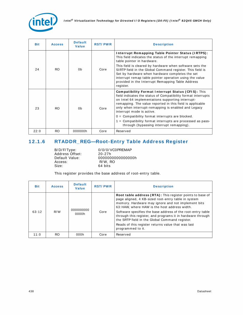
Intel® Virtualization Technology for Directed I/O Registers (D0:F0) (Intel® 82Q45 GMCH Only)
438 Datasheet
12.1.6 RTADDR_REG—Root-Entry Table Address Register
B/D/F/Type: 0/0/0/VC0PREMAPAddress Offset: 20-27hDefault Value: 0000000000000000hAccess: R/W, ROSize: 64 bits
This register provides the base address of root-entry table.
24 RO 0b Core
Interrupt Remapping Table Pointer Status (IRTPS): This field indicates the status of the interrupt remapping table pointer in hardware.This field is cleared by hardware when software sets the SIRTP field in the Global Command register. This field is Set by hardware when hardware completes the set interrupt remap table pointer operation using the value provided in the Interrupt Remapping Table Address register.
23 RO 0b Core
Compatibility Format Interrupt Status (CFIS): This field indicates the status of Compatibility format interrupts on Intel 64 implementations supporting interrupt-remapping. The value reported in this field is applicable only when interrupt-remapping is enabled and Legacy interrupt mode is active.0 = Compatibility format interrupts are blocked.1 = Compatibility format interrupts are processed as pass-
through (bypassing interrupt remapping).
22:0 RO 000000h Core Reserved
Bit AccessDefault Value
RST/PWR Description
Bit AccessDefault Value
RST/PWR Description
63:12 R/W000000000
0000hCore
Root table address (RTA): This register points to base of page aligned, 4 KB-sized root-entry table in system memory. Hardware may ignore and not implement bits 63:HAW, where HAW is the host address width.Software specifies the base address of the root-entry table through this register, and programs it in hardware through the SRTP field in the Global Command register.Reads of this register returns value that was last programmed to it.
11:0 RO 000h Core Reserved

Datasheet 439
Intel® Virtualization Technology for Directed I/O Registers (D0:F0) (Intel® 82Q45 GMCH Only)
12.1.7 CCMD_REG—Context Command Register
B/D/F/Type: 0/0/0/VC0PREMAPAddress Offset: 28-2FhDefault Value: 0000000000000000hAccess: W, R/W, ROSize: 64 bits
Register to manage context cache. The act of writing the uppermost byte of the CCMD_REG with ICC field set causes the hardware to perform the context-cache invalidation.
Bit AccessDefault Value
RST/PWR Description
63 R/W 0h Core
Invalidate Context-Cache (ICC): Software requests invalidation of context-cache by setting this field. Software must also set the requested invalidation granularity by programming the CIRG field.Software must read back and check the ICC field to be clear to confirm the invalidation is complete. Software must not update this register when this field is set.
Hardware clears the ICC field to indicate the invalidation request is complete. Hardware also indicates the granularity at which the invalidation operation was performed through the CAIG field. Software must not submit another invalidation request through this register while the ICC field is set.Software must submit a context cache invalidation request through this field only when there are no invalidation requests pending at this DMA-remapping hardware unit. Refer to Section 9 for software programming requirements.Since information from the context-cache may be used by hardware to tag IOTLB entries, software must perform domain-selective (or global) invalidation of IOTLB after the context cache invalidation has completed.Hardware implementations reporting write-buffer flushing requirement (RWBF=1 in Capability register) must implicitly perform a write buffer flushing before reporting invalidation complete to software through the ICC field. Refer to Section 9.1 for write buffer flushing requirements.

Intel® Virtualization Technology for Directed I/O Registers (D0:F0) (Intel® 82Q45 GMCH Only)
440 Datasheet
62:61 R/W 0h Core
Context Invalidation Request Granularity (CIRG): Software provides the requested invalidation granularity through this field when setting the ICC field.00 = Reserved.01 = Global Invalidation request.10 = Domain-selective invalidation request. The target
domain-ID must be specified in the DID field.11 = Device-selective invalidation request. The target source-ID(s) must be specified through the SID and FM fields, and the domain-ID (that was programmed in the context-entry for these device(s)) must be provided in the DID field.Hardware implementations may process an invalidation request by performing invalidation at a coarser granularity than requested. Hardware indicates completion of the invalidation request by clearing the ICC field. At this time, hardware also indicates the granularity at which the actual invalidation was performed through the CAIG field.
60:59 RO 0h Core
Context Actual Invalidation Granularity (CAIG): Hardware reports the granularity at which an invalidation request was processed through the CAIG field at the time of reporting invalidation completion (by clearing the ICC field).00 =Reserved.01= Global Invalidation performed. This could be in
response to a global, domain-selective or device-selective invalidation request.
10 =Domain-selective invalidation performed using the domain-ID specified by software in the DID field. This could be in response to a domain-selective or device-selective invalidation request.
11 =Device-selective invalidation performed using the source-ID and domain-ID specified by software in the SID and FM fields. This can only be in response to a device-selective invalidation request.
58:34 RO 000000000h Core Reserved
Bit AccessDefault Value
RST/PWR Description
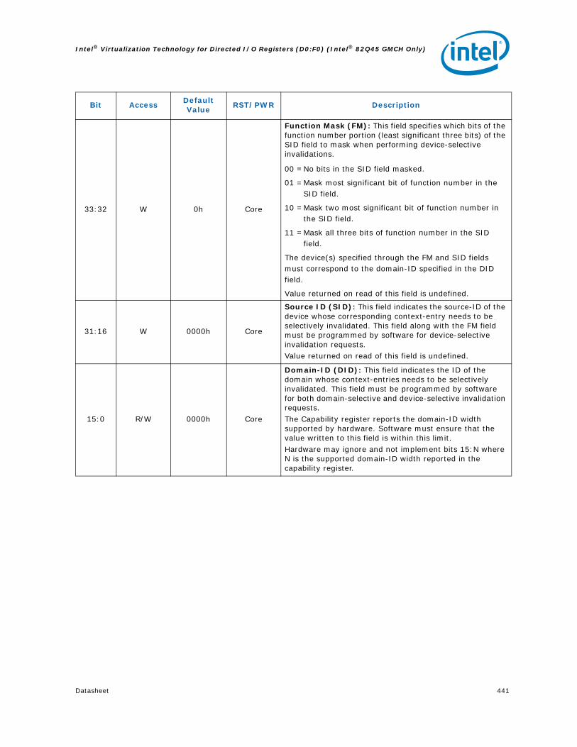
Datasheet 441
Intel® Virtualization Technology for Directed I/O Registers (D0:F0) (Intel® 82Q45 GMCH Only)
33:32 W 0h Core
Function Mask (FM): This field specifies which bits of the function number portion (least significant three bits) of the SID field to mask when performing device-selective invalidations.
00 =No bits in the SID field masked.
01 =Mask most significant bit of function number in the SID field.
10 =Mask two most significant bit of function number in the SID field.
11 =Mask all three bits of function number in the SID field.
The device(s) specified through the FM and SID fields must correspond to the domain-ID specified in the DID field.
Value returned on read of this field is undefined.
31:16 W 0000h Core
Source ID (SID): This field indicates the source-ID of the device whose corresponding context-entry needs to be selectively invalidated. This field along with the FM field must be programmed by software for device-selective invalidation requests.Value returned on read of this field is undefined.
15:0 R/W 0000h Core
Domain-ID (DID): This field indicates the ID of the domain whose context-entries needs to be selectively invalidated. This field must be programmed by software for both domain-selective and device-selective invalidation requests.The Capability register reports the domain-ID width supported by hardware. Software must ensure that the value written to this field is within this limit.Hardware may ignore and not implement bits 15:N where N is the supported domain-ID width reported in the capability register.
Bit AccessDefault Value
RST/PWR Description

Intel® Virtualization Technology for Directed I/O Registers (D0:F0) (Intel® 82Q45 GMCH Only)
442 Datasheet
12.1.8 FSTS_REG—Fault Status Register
B/D/F/Type: 0/0/0/VC0PREMAPAddress Offset: 34-37hDefault Value: 00000000hAccess: RO, RO/P, R/WC/PSize: 32 bits
This register indicates the primary fault logging status. Section 8.4.18.1 describes hardware behavior for primary fault logging.
Bit AccessDefault Value
RST/PWR Description
31:16 RO 0000h Core Reserved
15:8 RO/P 00h Core
Fault Record Index (FRI): This field is valid only when the PPF field is set. The FRI field indicates the index (from base) of the fault recording register to which the first pending fault was recorded when the PPF field was set by hardware. Valid values for this field are from 0 to N, where N is the value reported through NFR field in the Capability register.The value read from this field is undefined when the PPF field is clear.
7 RO 0b Core Reserved
6 RO 0b Core
Invalidation Time-out Error (ITE): Hardware detected a Device-IOTLB invalidation completion time-out. At this time, a fault event may be generated based on the programming of the Fault Event Control register.Hardware implementations not supporting Device-IOTLBs implement this bit as Reserved.
NOTE: This field is reserved as this feature is not supported.
5 RO 0b Core
Invalidation Completion Error (ICE): Hardware received an unexpected or invalid Device-IOTLB invalidation completion. This could be due to either an invalid ITag or invalid source-ID in an invalidation completion response. At this time, a fault event may be generated based on the programming of the Fault Event Control register.Hardware implementations not supporting Device-IOTLBs implement this bit as Reserved.
NOTE: This field is reserved as this feature is not supported.

Datasheet 443
Intel® Virtualization Technology for Directed I/O Registers (D0:F0) (Intel® 82Q45 GMCH Only)
4 RO 0b Core
Invalidation Queue Error (IQE): Hardware detected an error associated with the invalidation queue. This could be due to either a hardware error while fetching a descriptor from the invalidation queue, or hardware detecting an erroneous or invalid descriptor in the invalidation queue. At this time, a fault event may be generated based on the programming of the Fault Event Control register.Hardware implementations not supporting queued invalidations implement this bit as Reserved.
NOTE: This field is reserved as this feature is not supported.
3 RO 0b Core
Advanced Pending Fault (APF): When this field is Clear, hardware sets this field when the first fault record (at index 0) is written to a fault log. At this time, a fault event is generated based on the programming of the Fault Event Control register.Software writing 1 to this field clears it. Hardware implementations not supporting advanced fault logging implement this bit as Reserved.
NOTE: This field is reserved as this feature is not supported.
2 RO 0b Core
Advanced Fault Overflow (AFO): Hardware sets this field to indicate advanced fault log overflow condition. At this time, a fault event is generated based on the programming of the Fault Event Control register.Software writing 1 to this field clears it. Hardware implementations not supporting advanced fault logging implement this bit as Reserved.
NOTE: This field is reserved as this feature is not supported.
1 RO/P 0h Core
Primary Pending Fault (PPF): This field indicates if there are one or more pending faults logged in the fault recording registers. Hardware computes this field as the logical OR of Fault (F) fields across all the fault recording registers of this DMA-remapping hardware unit.0 = No pending faults in any of the fault recording
registers.1 = One or more fault recording registers has pending
faults. The FRI field is updated by hardware whenever the PPF field is set by hardware. Also, depending on the programming of Fault Event Control register, a fault event is generated when hardware sets this field.
0 R/WC/P 0h CorePrimary Fault Overflow (PFO): Hardware sets this field to indicate overflow of fault recording registers. Software writing 1 clears this field.
Bit AccessDefault Value
RST/PWR Description

Intel® Virtualization Technology for Directed I/O Registers (D0:F0) (Intel® 82Q45 GMCH Only)
444 Datasheet
12.1.9 FECTL_REG—Fault Event Control Register
B/D/F/Type: 0/0/0/VC0PREMAPAddress Offset: 38-3BhDefault Value: 80000000hAccess: R/W, ROSize: 32 bits
This register specifies the fault event interrupt message control bits.
Bit AccessDefault Value
RST/PWR Description
31 R/W 1h Core
Interrupt Mask (IM):0 = No masking of interrupt. When an interrupt condition
is detected, hardware issues an interrupt message (using the Fault Event Data and Fault Event Address register values).
1 = This is the value on reset. Software may mask interrupt message generation by setting this field. Hardware is prohibited from sending the interrupt message when this field is set.
30 RO 0h Core
Interrupt Pending (IP): Hardware sets the IP field whenever it detects an interrupt condition. Interrupt condition is defined as:• When primary fault logging is active, an interrupt
condition occurs when hardware records a fault through one of the Fault Recording registers and sets the PPF field in Fault Status register. If the PPF field was already set at the time of recording a fault, it is not treated as a new interrupt condition.
• When advanced fault logging is active, an interrupt condition occurs when hardware records a fault in the first fault record (at index 0) of the current fault log and sets the APF field in the Advanced Fault Log register. If the APF field was already set at the time of detecting/recording a fault, it is not treated as a new interrupt condition.
The IP field is kept set by hardware while the interrupt message is held pending. The interrupt message could be held pending due to interrupt mask (IM field) being set, or due to other transient hardware conditions.The IP field is cleared by hardware as soon as the interrupt message pending condition is serviced. This could be due to either:• Hardware issuing the interrupt message due to either
change in the transient hardware condition that caused interrupt message to be held pending or due to software clearing the IM field.
• Software servicing the interrupting condition through one of the following ways:— When primary fault logging is active, software
clearing the Fault (F) field in all the Fault Recording registers with faults, causing the PPF field in Fault Status register to be evaluated as clear.
— When advanced fault logging is active, software clearing the APF field in Advanced Fault Log register.
29:0 RO 00000000h Core Reserved

Datasheet 445
Intel® Virtualization Technology for Directed I/O Registers (D0:F0) (Intel® 82Q45 GMCH Only)
12.1.10 FEDATA_REG—Fault Event Data Register
B/D/F/Type: 0/0/0/VC0PREMAPAddress Offset: 3C-3FhDefault Value: 00000000hAccess: RO, R/WSize: 32 bits
This Register specifies the interrupt message data.
12.1.11 FEADDR_REG—Fault Event Address Register
B/D/F/Type: 0/0/0/VC0PREMAPAddress Offset: 40-43hDefault Value: 00000000hAccess: RO, R/WSize: 32 bits
This register specifies the interrupt message address.
Bit AccessDefault Value
RST/PWR Description
31:16 RO 0000h Core
Extended Interrupt Message Data (EIMD): This field is valid only for implementations supporting 32-bit MSI data fields.Hardware implementations supporting only 16-bit MSI data may treat this field as read only (0).
15:0 R/W 0000h CoreInterrupt message data (IMD): Data value in the fault-event interrupt message.
Bit AccessDefault Value
RST/PWR Description
31:2 R/W 00000000h CoreMessage address (MA): When fault events are enabled, the contents of this register specify the DWord aligned address (bits 31:2) for the MSI memory write transaction.
1:0 RO 0h Core Reserved

Intel® Virtualization Technology for Directed I/O Registers (D0:F0) (Intel® 82Q45 GMCH Only)
446 Datasheet
12.1.12 FEUADDR_REG—Fault Event Upper Address Register
B/D/F/Type: 0/0/0/VC0PREMAPAddress Offset: 44-47hDefault Value: 00000000hAccess: ROSize: 32 bits
This register specifies the interrupt message address. For platforms supporting only interrupt messages in the 32-bit address range, this register is treated as read-only (0).
Bit AccessDefault Value
RST/PWR Description
31:0 RO 00000000h Core
Message upper address (MUA): This field needs to be implemented only if hardware supports 64-bit message address. If implemented, the contents of this register specify the upper 32-bits of a 64- bit MSI write transaction.If hardware does not support 64-bit messages, the register is treated as read only (0).
NOTE: This field is reserved as this feature is not supported.

Datasheet 447
Intel® Virtualization Technology for Directed I/O Registers (D0:F0) (Intel® 82Q45 GMCH Only)
12.1.13 AFLOG_REG—Advanced Fault Log Register
B/D/F/Type: 0/0/0/VC0PREMAPAddress Offset: 58-5FhDefault Value: 0000000000000000hAccess: ROSize: 64 bits
This register specifies the base address of memory-resident fault-log region. This register is treated as read only (0) for implementations not supporting advanced translation fault logging (AFL field reported as 0 in the Capability register). This register is sticky and can be cleared only through powergood reset or via software clearing the RW1C fields by writing a 1.
Bit AccessDefault Value
RST/PWR Description
63:12 RO000000000
0000hCore
Fault Log Address (FLA): This field specifies the base of size-aligned fault-log region in system memory. Hardware may ignore and not implement bits 63:HAW, where HAW is the host address width.
Software specifies the base address and size of the fault log region through this register, and programs it in hardware through the SFL field in the Global Command register. When implemented, reads of this field returns value that was last programmed to it.
NOTE: This field is reserved as this feature is not supported.
11:9 RO 0h Core
Fault Log Size (FLS): This field specifies the size of the fault log region pointed by the FLA field.The size of the fault log region is 2X * 4KB, where X is the value programmed in this register. When implemented, reads of this field returns value that was last programmed to it.
NOTE: This field is reserved as this feature is not supported.
8:0 RO 0s Core Reserved

Intel® Virtualization Technology for Directed I/O Registers (D0:F0) (Intel® 82Q45 GMCH Only)
448 Datasheet
12.1.14 PMEN_REG—Protected Memory Enable Register
B/D/F/Type: 0/0/0/VC0PREMAPAddress Offset: 64-67hDefault Value: 00000000hAccess: RO, R/WSize: 32 bits
This register is used to enable the DMA protected memory regions setup through the PLMBASE, PLMLIMT, PHMBASE, PHMLIMIT registers. When LT.CMD.LOCK.PMRC command is invoked, this register is locked (treated RO). When LT.CMD.UNLOCK.PMRC command is invoked, this register is unlocked (treated as R/W). This register is always treated as RO (0) for implementations not supporting protected memory regions (PLMR and PHMR fields reported as 0 in the Capability register).
Bit AccessDefault Value
RST/PWR Description
31 R/W 0h Core
Enable Protected Memory (EPM): This field controls DMA accesses to the protected low-memory and protected high-memory regions.
0 = DMA accesses to protected memory regions are handled as follows:— If DMA-remapping hardware is not enabled, DMA
requests (including those to protected regions) are not blocked.
— If DMA-remapping hardware is enabled, DMA requests are translated per the programming of the DMA-remapping structures. Software may program the DMA-remapping structures to allow or block DMA to the protected memory regions.
1 = DMA accesses to protected memory regions are handled as follows:— If DMA-remapping hardware is not enabled, DMA to
protected memory regions are blocked. These DMA requests are not recorded or reported as DMA-remapping faults.
— If DMA-remapping hardware is enabled, hardware may or may not block DMA to the protected memory region(s). Software must not depend on hardware protection of the protected memory regions, and must ensure the DMA-remapping structures are properly programmed to not allow DMA to the protected memory regions.
Hardware reports the status of the protected memory enable/disable operation through the PRS field in this register.Hardware implementations supporting DMA draining must drain any in-flight translated DMA requests queued within the root complex before indicating the protected memory region as enabled through the PRS field.
30:1 RO 00000000h Core Reserved
0 RO 0h Core
Protected Region Status (PRS): This field indicates the status of protected memory region.0 = Protected memory region(s) not enabled.1 = Protected memory region(s) enabled.

Datasheet 449
Intel® Virtualization Technology for Directed I/O Registers (D0:F0) (Intel® 82Q45 GMCH Only)
12.1.15 PLMBASE_REG—Protected Low-Memory Base Register
B/D/F/Type: 0/0/0/VC0PREMAPAddress Offset: 68-6BhDefault Value: 00000000hAccess: R/W, ROSize: 32 bits
This register is used to setup the base address of DMA protected low-memory region. This register must be setup before enabling protected memory through PMEN_REG, and must not be updated when protected memory regions are enabled.
When LT.CMD.LOCK.PMRC command is invoked, this register is locked (treated RO). When LT.CMD.UNLOCK.PMRC command is invoked, this register is unlocked (treated as R/W). This register is always treated as RO for implementations not supporting protected low memory region (PLMR field reported as 0 in the Capability register). The alignment of the protected low memory region base depends on the number of reserved bits (N) of this register. Software may determine the value of N by writing all 1's to this register, and finding most significant zero bit position with 0 in the value read back from the register. Bits N:0 of this register is decoded by hardware as all 0s.
Bit AccessDefault Value
RST/PWR Description
31:21 R/W 000h Core
Protected Low-Memory Base (PLMB): This register specifies the base of size aligned, protected low-memory region in system memory. The protected low-memory region has a minimum size of 2 MB and must be size aligned.
20:0 RO 000000h Core Reserved

Intel® Virtualization Technology for Directed I/O Registers (D0:F0) (Intel® 82Q45 GMCH Only)
450 Datasheet
12.1.16 PLMLIMIT_REG—Protected Low-Memory Limit Register
B/D/F/Type: 0/0/0/VC0PREMAPAddress Offset: 6C-6FhDefault Value: 00000000hAccess: R/W, ROSize: 32 bits
This register is used to setup the limit address of DMA protected low-memory region. This register must be setup before enabling protected memory through PMEN_REG, and must not be updated when protected memory regions are enabled.
When LT.CMD.LOCK.PMRC command is invoked, this register is locked (treated RO).
When LT.CMD.UNLOCK.PMRC command is invoked, this register is unlocked (treated as R/W).
This register is always treated as RO for implementations not supporting protected low memory region (PLMR field reported as 0 in the Capability register). The alignment of the protected low memory region limit depends on the number of reserved bits (N) of this register. Software may determine the value of N by writing all 1s to this register, and finding most significant zero bit position with 0 in the value read back from the register. Bits N:0 of the limit register are decoded by hardware as all 1s. The Protected low-memory base and limit registers functions as follows:
• Programming the protected low-memory base and limit registers with the same value in bits 31:(N+1) specifies a protected low-memory region of size 2(N+1) bytes.
• Programming the protected low-memory limit register with a value less than the protected low-memory base register disables the protected low-memory region.
Bit AccessDefault Value
RST/PWR Description
31:21 R/W 000h CoreProtected Low-Memory Limit (PLML): This field specifies the last host physical address of the DMA protected low-memory region in system memory.
20:0 RO 000000h Core Reserved

Datasheet 451
Intel® Virtualization Technology for Directed I/O Registers (D0:F0) (Intel® 82Q45 GMCH Only)
12.1.17 PHMBASE_REG—Protected High-Memory Base Register
B/D/F/Type: 0/0/0/VC0PREMAPAddress Offset: 70-77hDefault Value: 0000000000000000hAccess: RO, R/WSize: 64 bits
This register is used to setup the base address of DMA protected high-memory region. This register must be setup before enabling protected memory through PMEN_REG, and must not be updated when protected memory regions are enabled. When LT.CMD.LOCK.PMRC command is invoked, this register is locked (treated RO). When LT.CMD.UNLOCK.PMRC command is invoked, this register is unlocked (treated as R/W). This register is always treated as RO for implementations not supporting protected high memory region (PHMR field reported as 0 in the Capability register). The alignment of the protected high memory region base depends on the number of reserved bits (N) of this register. Software may determine the value of N by writing all 1s to this register, and finding most significant zero bit position below host address width (HAW) in the value read back from the register. Bits N:0 of the limit register is decoded by hardware as all 0s.
Bit AccessDefault Value
RST/PWR Description
63:21 R/W000000000
00hCore
Protected High-Memory Base (PHMB): This register specifies the base of size aligned, protected memory region in system memory. Hardware may not use bits 63:HAW, where HAW is the host address width.The protected high-memory region has a minimum size of 2 MB and must be size aligned.
20:0 RO 000000h Core Reserved
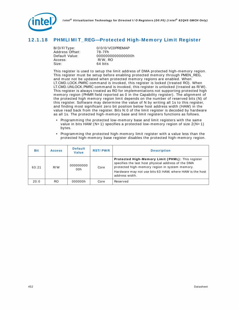
Intel® Virtualization Technology for Directed I/O Registers (D0:F0) (Intel® 82Q45 GMCH Only)
452 Datasheet
12.1.18 PHMLIMIT_REG—Protected High-Memory Limit Register
B/D/F/Type: 0/0/0/VC0PREMAPAddress Offset: 78-7FhDefault Value: 0000000000000000hAccess: R/W, ROSize: 64 bits
This register is used to setup the limit address of DMA protected high-memory region. This register must be setup before enabling protected memory through PMEN_REG, and must not be updated when protected memory regions are enabled. When LT.CMD.LOCK.PMRC command is invoked, this register is locked (treated RO). When LT.CMD.UNLOCK.PMRC command is invoked, this register is unlocked (treated as R/W). This register is always treated as RO for implementations not supporting protected high memory region (PHMR field reported as 0 in the Capability register). The alignment of the protected high memory region limit depends on the number of reserved bits (N) of this register. Software may determine the value of N by writing all 1s to this register, and finding most significant zero bit position below host address width (HAW) in the value read back from the register. Bits N:0 of the limit register is decoded by hardware as all 1s. The protected high-memory base and limit registers functions as follows.
• Programming the protected low-memory base and limit registers with the same value in bits HAW:(N+1) specifies a protected low-memory region of size 2(N+1) bytes.
• Programming the protected high-memory limit register with a value less than the protected high-memory base register disables the protected high-memory region.
Bit AccessDefault Value
RST/PWR Description
63:21 R/W000000000
00hCore
Protected High-Memory Limit (PHML): This register specifies the last host physical address of the DMA protected high-memory region in system memory.Hardware may not use bits 63:HAW, where HAW is the host address width.
20:0 RO 000000h Core Reserved

Datasheet 453
Intel® Virtualization Technology for Directed I/O Registers (D0:F0) (Intel® 82Q45 GMCH Only)
12.1.19 IVA_REG—Invalidate Address Register
B/D/F/Type: 0/0/0/VC0PREMAPAddress Offset: 100-107hDefault Value: 0000000000000000hAccess: W, ROSize: 64 bits
This register provides the DMA address whose corresponding IOTLB entry needs to be invalidated through the corresponding IOTLB Invalidate register. This register is a write only register. The value returned on reads of this register is undefined. There is an IVA_REG for each IOTLB Invalidation unit supported by hardware.
Bit AccessDefault Value
RST/PWR Description
63:12 W000000000
0000hCore
Address (Addr): Software provides the DMA address that needs to be page-selectively invalidated. To request a page-selective invalidation request to hardware, software must first write the appropriate fields in this register, and then issue appropriate page-selective invalidate command through the IOTLB_REG.Hardware ignores bits 63:N, where N is the maximum guest address width (MGAW) supported.Value returned on read of this field is undefined.
11:7 RO 00h Core Reserved
6 W 0h Core
Invalidation Hint (IH): The field provides hints to hardware to preserve or flush the non-leaf (page-directory) entries that may be cached in hardware.0 = Software may have modified both leaf and non-leaf
page-table entries corresponding to mappings specified in the ADDR and AM fields. On a pageselective invalidation request, hardware must flush both the cached leaf and non-leaf page-table Value returned on read of this field is undefined. entries corresponding to mappings specified by ADDR and AM fields.
1 = Software has not modified any non-leaf page-table entries corresponding to mappings specified in the ADDR and AM fields. On a page-selective invalidation request, hardware may preserve the cached non-leaf page-table entries corresponding to mappings specified by ADDR and AM fields.

Intel® Virtualization Technology for Directed I/O Registers (D0:F0) (Intel® 82Q45 GMCH Only)
454 Datasheet
5:0 W 00h Core
Address Mask (AM): The value in this field specifies the number of low order bits of the ADDR field that must be masked for the invalidation operation. Mask field enables software to request invalidation of contiguous mappings for size-aligned regions. For example: Mask Value ADDR bits masked Pages invalidated Mask Value Addr bits masked Pg inval 0 Nil 1 1 12 2 2 13:12 4 3 14:12 8 4 15:12 16 5 16:12 32 6 17:12 64 7 18:12 128 8 19:12 256Hardware implementations report the maximum supported mask value through the Capability register. Value returned on read of this field is undefined.
Bit AccessDefault Value
RST/PWR Description

Datasheet 455
Intel® Virtualization Technology for Directed I/O Registers (D0:F0) (Intel® 82Q45 GMCH Only)
12.2 DMI VC1 Remap Engine Registers
Table 27. DMI VC1 Remap Engine Register Address Map
Address Offset
Register Symbol
Register NameDefault Value
Access
0–3h VER_REG Version Register 00000010h RO
8–Fh CAP_REG Capability Register00C9008020
E30272h RO
10–17h ECAP_REG Extended Capability Register0000000000
001000h RO
18–1Bh GCMD_REG Global Command Register 00000000h RO, W
1C–1Fh GSTS_REG Global Status Register 00000000h RO
20–27h RTADDR_REG Root-Entry Table Address Register0000000000
000000h R/W, RO
28–2Fh CCMD_REG Context Command Register0000000000
000000h RO, R/W, W
34–37h FSTS_REG Fault Status Register 00000000h RO, RO/P, R/WC/P
38–3Bh FECTL_REG Fault Event Control Register 80000000h RO, R/W
3C–3Fh FEDATA_REG Fault Event Data Register 00000000h RO, R/W
40–43h FEADDR_REG Fault Event Address Register 00000000h R/W, RO
44–h FEUADDR_REGFault Event Upper Address Register
00000000h RO
58–5Fh AFLOG_REG Advanced Fault Log Register0000000000
000000h RO
64–67h PMEN_REG Protected Memory Enable Register 00000000h RO, R/W
68–6Bh PLMBASE_REGProtected Low-Memory Base Register
00000000h R/W, RO
6C–6Fh PLMLIMIT_REGProtected Low-Memory Limit Register
00000000h R/W, RO
70–77h PHMBASE_REGProtected High-Memory Base Register
0000000000000000h
R/W, RO
78–7FhPHMLIMIT_RE
GProtected High-Memory Limit Register
0000000000000000h
RO, R/W
100–107h IVA_REG Invalidate Address Register0000000000
000000h W, RO
108–10Fh IOTLB_REG IOTLB Invalidate Register0000000000
000000h R/W, RO
200–20Fh FRCD_REG Fault Recording Registers
000000000000000000000000000000
00h
RO, RO/P, R/WC/P
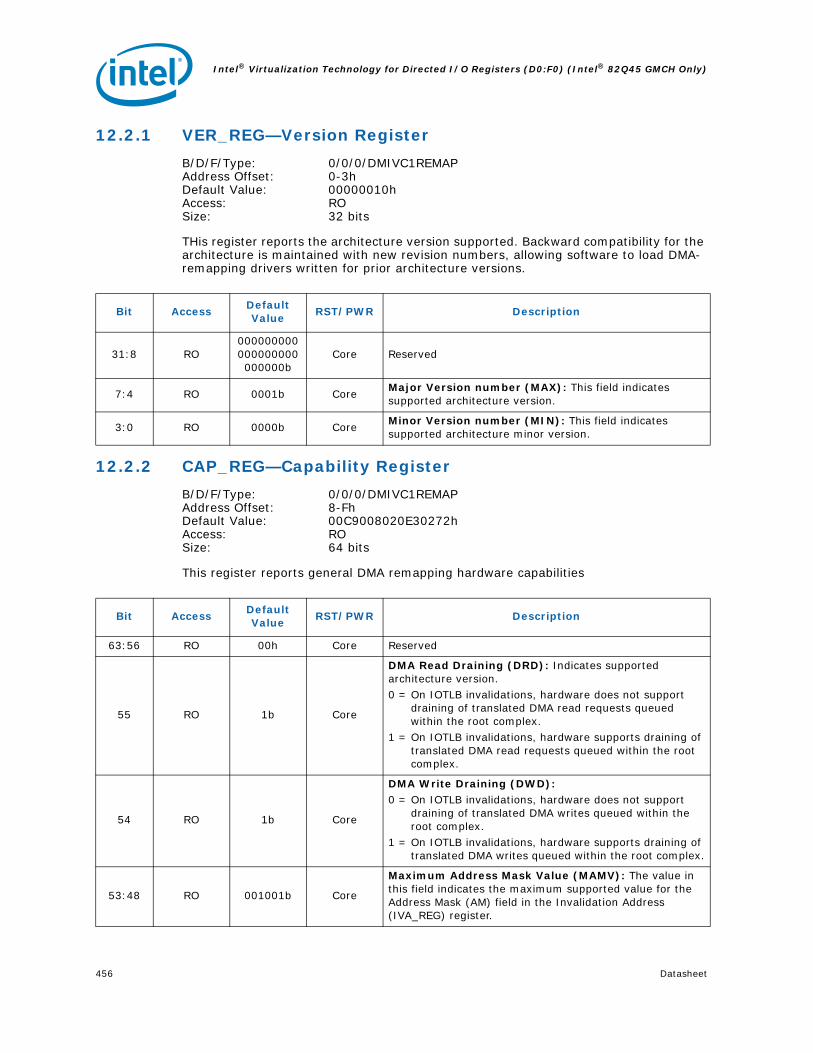
Intel® Virtualization Technology for Directed I/O Registers (D0:F0) (Intel® 82Q45 GMCH Only)
456 Datasheet
12.2.1 VER_REG—Version Register
B/D/F/Type: 0/0/0/DMIVC1REMAPAddress Offset: 0-3hDefault Value: 00000010hAccess: ROSize: 32 bits
THis register reports the architecture version supported. Backward compatibility for the architecture is maintained with new revision numbers, allowing software to load DMA-remapping drivers written for prior architecture versions.
12.2.2 CAP_REG—Capability Register
B/D/F/Type: 0/0/0/DMIVC1REMAPAddress Offset: 8-FhDefault Value: 00C9008020E30272hAccess: ROSize: 64 bits
This register reports general DMA remapping hardware capabilities
Bit AccessDefault Value
RST/PWR Description
31:8 RO000000000000000000000000b
Core Reserved
7:4 RO 0001b CoreMajor Version number (MAX): This field indicates supported architecture version.
3:0 RO 0000b CoreMinor Version number (MIN): This field indicates supported architecture minor version.
Bit AccessDefault Value
RST/PWR Description
63:56 RO 00h Core Reserved
55 RO 1b Core
DMA Read Draining (DRD): Indicates supported architecture version.0 = On IOTLB invalidations, hardware does not support
draining of translated DMA read requests queued within the root complex.
1 = On IOTLB invalidations, hardware supports draining of translated DMA read requests queued within the root complex.
54 RO 1b Core
DMA Write Draining (DWD): 0 = On IOTLB invalidations, hardware does not support
draining of translated DMA writes queued within the root complex.
1 = On IOTLB invalidations, hardware supports draining of translated DMA writes queued within the root complex.
53:48 RO 001001b Core
Maximum Address Mask Value (MAMV): The value in this field indicates the maximum supported value for the Address Mask (AM) field in the Invalidation Address (IVA_REG) register.

Datasheet 457
Intel® Virtualization Technology for Directed I/O Registers (D0:F0) (Intel® 82Q45 GMCH Only)
47:40 RO 00000000b Core
Number of Faultrecording Registers (NFR): This field indicates a value of N-1, where N is the number of fault recording registers supported by hardware.Implementations must support at least one fault recording register (NFR = 0) for each DMAremapping hardware unit in the platform.The maximum number of fault recording registers per DMA-remapping hardware unit is 256.
39 RO 1b Core
Page Selective Invalidation Support (PSI):
0 = Indicates that the DMAr engine does not support page selective invalidations
1 = Indicates the DMAr engine does support page-selective IOTLB invalidations. The MAMV field indicates the maximum number of contiguous translations that may be invalidated in a single request.
38 RO 0b Core Reserved
37:34 RO 0000b Core
Super page Support (SPS): This field indicates the super page sizes supported by hardware.A value of 1 in any of these bits indicates the corresponding super-page size is supported. The super-page sizes corresponding to various bit positions within this field are:0 = 21-bit offset to page frame1 = 30-bit offset to page frame2 = 39-bit offset to page frame3 = 48-bit offset to page frame
33:24 RO 020h Core
Fault-recording Register offset (FRO): This field specifies the location to the first fault recording register relative to the register base address of this DMA-remapping hardware unit. If the register base address is X, and the value reported in this field is Y, the address for the first fault recording register is calculated as X+(16*Y).
23 RO 1b Core
Isochrony (Isoch): 0 = Indicates this DMA-remapping hardware unit has no
critical isochronous requesters in its scope.1 = Indicates this DMA-remapping hardware unit has one
or more critical isochronous requesters in its scope. To ensure isochronous performance, software must ensure invalidation operations do not impact active DMA streams. This implies that when DMA is active, software perform page-selective invalidations (instead of coarser invalidations).
22 RO 1b Core
Zero Length Read (ZLR):0 = Indicates the remapping hardware unit blocks (and
treats as fault) zero length DMA read requests to write-only pages.
1 = Indicates the remapping hardware unit supports zero length DMA read requests to write-only pages.
Bit AccessDefault Value
RST/PWR Description

Intel® Virtualization Technology for Directed I/O Registers (D0:F0) (Intel® 82Q45 GMCH Only)
458 Datasheet
21:16 RO 100011b Core
Maximum Guest Address Width (MGAW): This field indicates the maximum DMA virtual addressability supported by remapping hardware.The Maximum Guest Address Width (MGAW) is computed as (N+1), where N is the value reported in this field. For example, a hardware implementation supporting 48-bit MGAW reports a value of 47 (101111b) in this field.If the value in this field is X, DMA requests to addresses above 2(x+1)-1 are always blocked by hardware.Guest addressability for a given DMA request is limited to the minimum of the value reported through this field and the adjusted guest address width of the corresponding page-table structure. (Adjusted guest address widths supported by hardware are reported through the SAGAW field).
15:13 RO 000b Core Reserved
12:8 RO 00010b Core
Supported Adjusted Guest Address Widths (SAGAW): This 5-bit field indicates the supported adjusted guest address widths (which in turn represents the levels of page-table walks) supported by the hardware implementation.A value of 1 in any of these bits indicates the corresponding adjusted guest address width is supported. The adjusted guest address widths corresponding to various bit positions within this field are:0 = 30-bit AGAW (2-level page table)1 = 39-bit AGAW (3-level page table)2 = 48-bit AGAW (4-level page table)3 = 57-bit AGAW (5-level page table)4 = 64-bit AGAW (6-level page table)Software must ensure that the adjusted guest address width used to setup the page tables is one of the supported guest address widths reported in this field.
7 RO 0b Core
Caching Mode (CM):0 = Hardware does not cache not present and erroneous
entries in the context-cache and IOTLB. Invalidations are not required for modifications to individual not present or invalid entries. However, any modifications that result in decreasing the effective permissions or partial permission increases require invalidations for them to be effective.
1 = Hardware may cache not present and erroneous mappings in the context-cache or IOTLB. Any software updates to the DMA-remapping structures (including updates to not-present or erroneous entries) require explicit invalidation.
Hardware implementations are recommended to support operation corresponding to CM=0.
Bit AccessDefault Value
RST/PWR Description

Datasheet 459
Intel® Virtualization Technology for Directed I/O Registers (D0:F0) (Intel® 82Q45 GMCH Only)
6 RO 1b Core
Protected High-Memory Region (PHMR):0 = Indicates protected high-memory region not
supported.1 = Indicates protected high-memory region is supported.DMA-remapping hardware implementations on Intel TXT platforms supporting main memory above 4 GB are required to support protected high-memory region.
5 RO 1b Core
Protected Low-Memory Region (PLMR):0 = 0: Indicates protected low-memory region not
supported.1 = 1: Indicates protected low-memory region is
supported.DMA-remapping hardware implementations on Intel TXT platforms are required to support protected low-memory region.
4 RO 1b Core
Required Write-Buffer Flushing (RWBF):0 = Indicates no write-buffer flushing needed to ensure
changes to memory-resident structures are visible to hardware.
1 = Indicates software must explicitly flush the write buffers (through the Global Command register) to ensure updates made to memory-resident
DMA-remapping structures are visible to hardware.
3 RO 0b Core
Advanced Fault Logging (AFL):0 = Indicates advanced fault logging not supported. Only
primary fault logging is supported.1 = Indicates advanced fault logging is supported.
2:0 RO 010b Core
Number of domains supported (ND):000 =Hardware supports 4-bit domain-IDs with support
for up to 16 domains.001 =Hardware supports 6-bit domain-IDs with support
for up to 64 domains.010 =Hardware supports 8-bit domain-IDs with support
for up to 256 domains.011 =Hardware supports 10-bit domain-IDs with support
for up to 1024 domains.100 =Hardware supports 12-bit domain-IDs with support
for up to 4K domains.100 =Hardware supports 14-bit domain-IDs with support
for up to 16K domains.110 =Hardware supports 16-bit domain-IDs with support
for up to 64K domains.111 =Reserved.
Bit AccessDefault Value
RST/PWR Description

Intel® Virtualization Technology for Directed I/O Registers (D0:F0) (Intel® 82Q45 GMCH Only)
460 Datasheet
12.2.3 ECAP_REG—Extended Capability Register
B/D/F/Type: 0/0/0/DMIVC1REMAPAddress Offset: 10-17hDefault Value: 0000000000001000hAccess: ROSize: 64 bits
This register reports DMA-remapping hardware extended capabilities
Bit AccessDefault Value
RST/PWR Description
63:24 RO 0s Core Reserved
23:20 RO 0000b Core
Maximum Handle Mask Value (MHMV): The value in this field indicates the maximum supported value for the Handle Mask (HM) field in the interrupt entry cache invalidation descriptor (iec_inv_dsc).This field is valid only when the IR field is reported as Set.
19:18 RO 00b Core Reserved
17:8 RO 010h Core
Invalidation Unit Offset (IVO): This field specifies the location to the first IOTLB invalidation unit relative to the register base address of this DMA-remapping hardware unit. If the register base address is X, and the value reported in this field is Y, the address for the first IOTLB invalidation unit is calculated as X+(16*Y).If N is the value reported in NIU field, the address for the last IOTLB invalidation unit is calculated as X+(16*Y)+(16*N).
7 RO 0b Core
Snoop Control (SC): 0 = Hardware does not support 1-setting of the SNP field
in the page-table entries.1 = Hardware supports the 1-setting of the SNP field in the
page-table entries.
6 RO 0b Core
Pass Through (PT): 0 = Hardware does not support passthrough translation
type in context entries.1 = Hardware supports pass-through translation type in
context entries.
5 RO 0b Core
Caching Hints (CH):0 = Hardware does not support IOTLB caching hints (ALH
and EH fields in context-entries are treated as reserved).
1 = Hardware supports IOLTB caching hints through the ALH and EH fields in context-entries.
4 RO 0b Core
Extended Interrupt Mode (EIM):0 = Hardware supports only 8-bit APICIDs (Legacy
Interrupt Mode) on Intel®64 and IA-32 platforms and 16- bit APIC-IDs on ItaniumTM platforms.
1 = Hardware supports Extended Interrupt Mode (32-bit APIC-IDs) on Intel®64 platforms.
This field is valid only when the IR field is reported as Set.

Datasheet 461
Intel® Virtualization Technology for Directed I/O Registers (D0:F0) (Intel® 82Q45 GMCH Only)
3 RO 0b Core
Interrupt Remapping Support (IR):0 = Hardware does not support interrupt remapping.1 = Hardware supports interrupt remapping.Implementations reporting this field as Set must also support Queued Invalidation (QI = 1b).
2 RO 0b Core
Device IOTLB Support (DI): 0 = Hardware does not support device- IOTLBs.1 = Hardware supports Device-IOTLBs.Implementations reporting this field as Set must also support Queued Invalidation (QI = 1b).
NOTE: This field is reserved as this feature is not supported.
1 RO 0b CoreQueued Invalidation Support (QI): 0 = Hardware does not support queued invalidations.1 = Hardware supports queued invalidations.
0 RO 0b Core
Coherency (C):
0 = Hardware accesses to the root, context, and page table structures are non-coherent (non-snoop).
1 = Hardware accesses to the root, context, and page table structures are coherent (snoop).
Hardware writes to the advanced fault log is required to be coherent.
Bit AccessDefault Value
RST/PWR Description

Intel® Virtualization Technology for Directed I/O Registers (D0:F0) (Intel® 82Q45 GMCH Only)
462 Datasheet
12.2.4 GCMD_REG—Global Command Register
B/D/F/Type: 0/0/0/DMIVC1REMAPAddress Offset: 18-1BhDefault Value: 00000000hAccess: RO, WSize: 32 bits
This register controls DMA-remapping hardware. If multiple control fields in this register need to be modified, software must serialize through multiple writes to this register.
Bit AccessDefault Value
RST/PWR Description
31 W 0b Core
Translation Enable (TE): Software writes to this field to request hardware to enable/disable DMA-remapping hardware.0 = Disable DMA-remapping hardware1 = Enable DMA-remapping hardwareHardware reports the status of the translation enable operation through the TES field in the Global Status register.Before enabling (or re-enabling) DMA-remapping hardware through this field, software must:• Setup the DMA-remapping structures in memory• Flush the write buffers (through WBF field), if write
buffer flushing is reported as required.• Set the root-entry table pointer in hardware (through
SRTP field).• Perform global invalidation of the context-cache and
global invalidation of IOTLB• If advanced fault logging supported, setup fault log
pointer (through SFL field) and enable advanced fault logging (through EAFL field).
There may be active DMA requests in the platform when software updates this field. Hardware must enable or disable remapping logic only at deterministic transaction boundaries, so that any in-flight transaction is either subject to remapping or not at all.Hardware implementations supporting DMA draining must drain any in-flight translated DMA read/write requests queued within the root complex before completing the translation enable command and reflecting the status of the command through the TES field in the GSTS_REG.Value returned on read of this field is undefined.
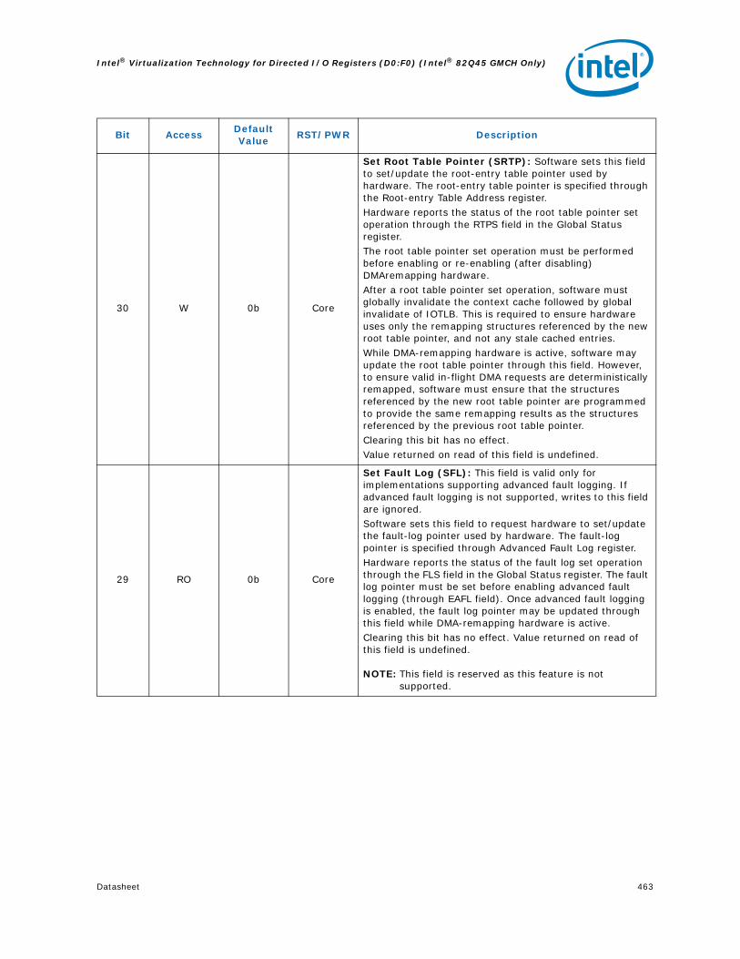
Datasheet 463
Intel® Virtualization Technology for Directed I/O Registers (D0:F0) (Intel® 82Q45 GMCH Only)
30 W 0b Core
Set Root Table Pointer (SRTP): Software sets this field to set/update the root-entry table pointer used by hardware. The root-entry table pointer is specified through the Root-entry Table Address register.Hardware reports the status of the root table pointer set operation through the RTPS field in the Global Status register.The root table pointer set operation must be performed before enabling or re-enabling (after disabling) DMAremapping hardware. After a root table pointer set operation, software must globally invalidate the context cache followed by global invalidate of IOTLB. This is required to ensure hardware uses only the remapping structures referenced by the new root table pointer, and not any stale cached entries.While DMA-remapping hardware is active, software may update the root table pointer through this field. However, to ensure valid in-flight DMA requests are deterministically remapped, software must ensure that the structures referenced by the new root table pointer are programmed to provide the same remapping results as the structures referenced by the previous root table pointer.Clearing this bit has no effect.Value returned on read of this field is undefined.
29 RO 0b Core
Set Fault Log (SFL): This field is valid only for implementations supporting advanced fault logging. If advanced fault logging is not supported, writes to this field are ignored. Software sets this field to request hardware to set/update the fault-log pointer used by hardware. The fault-log pointer is specified through Advanced Fault Log register.Hardware reports the status of the fault log set operation through the FLS field in the Global Status register. The fault log pointer must be set before enabling advanced fault logging (through EAFL field). Once advanced fault logging is enabled, the fault log pointer may be updated through this field while DMA-remapping hardware is active.Clearing this bit has no effect. Value returned on read of this field is undefined.
NOTE: This field is reserved as this feature is not supported.
Bit AccessDefault Value
RST/PWR Description

Intel® Virtualization Technology for Directed I/O Registers (D0:F0) (Intel® 82Q45 GMCH Only)
464 Datasheet
28 RO 0b Core
Enable Advanced Fault Logging (EAFL): This field is valid only for implementations supporting advanced fault logging. If advanced fault logging is not supported, writes to this field are ignored.Software writes to this field to request hardware to enable or disable advanced fault logging.0 = Disable advanced fault logging. In this case,
translation faults are reported through the Fault Recording registers.
1 = Enable use of memory-resident fault log. When enabled, translation faults are recorded in the memory-resident log. The fault log pointer must be set in hardware (through SFL field) before enabling advanced fault logging.
Hardware reports the status of the advanced fault logging enable operation through the AFLS field in the Global Status register.Value returned on read of this field is undefined.
NOTE: This field is reserved as this feature is not supported.
27 W 0b Core
Write Buffer Flush (WBF): This bit is valid only for implementations requiring write buffer flushing. If write buffer flushing is not required, writes to this field are ignored.Software sets this field to request hardware to flush the root-complex internal write buffers. This is done to ensure any updates to the memory-resident DMA-remapping structures are not held in any internal write posting buffers. Refer to Section 9.1 for details on write-buffer flushing requirements.Hardware reports the status of the write buffer flushing operation through the WBFS field in the Global Status register.Clearing this bit has no effect. Value returned on read of this field is undefined.
NOTE: This field is reserved as this feature is not supported.
26 RO 0b Core
Queued Invalidation Enable (QIE): This field is valid only for implementations supporting queued invalidations.Software writes to this field to enable or disable queued invalidations.0 = Disable queued invalidations.1 = Enable use of queued invalidations.Hardware reports the status of queued invalidation enable operation through QIES field in the Global Status register.Refer to Section 6.2.2 for software requirements for enabling/disabling queued invalidations.The value returned on a read of this field is undefined.
NOTE: This field is reserved as this feature is not supported.
Bit AccessDefault Value
RST/PWR Description

Datasheet 465
Intel® Virtualization Technology for Directed I/O Registers (D0:F0) (Intel® 82Q45 GMCH Only)
25 RO 0b Core
Interrupt Remapping Enable (IRE): This field is valid only for implementations supporting interrupt remapping.0 = Disable interrupt-remapping hardware1 = Enable interrupt-remapping hardwareHardware reports the status of the interrupt remapping enable operation through the IRES field in the Global Status register.There may be active interrupt requests in the platform when software updates this field. Hardware must enable or disable interrupt-remapping logic only at deterministic transaction boundaries, so that any in-flight interrupts are either subject to remapping or not at all.Hardware implementations must drain any in-flight interrupts requests queued in the Root-Complex before completing the interrupt-remapping enable command and reflecting the status of the command through the IRES field in the Global Status register.The value returned on a read of this field is undefined.
NOTES:This field is reserved as this feature is not supported.
24 RO 0b Core
Set Interrupt Remap Table Pointer (SIRTP): This field is valid only for implementations supporting interrupt-remapping.Software sets this field to set/update the interrupt remapping table pointer used by hardware. The interrupt remapping table pointer is specified through the Interrupt Remapping Table Address register.Hardware reports the status of the interrupt remapping table pointer set operation through the IRTPS field in the Global Status register. The interrupt remap table pointer set operation must be performed before enabling or re-enabling (after disabling) interrupt-remapping hardware through the IRE field.After an interrupt remap table pointer set operation, software must globally invalidate the interrupt entry cache. This is required to ensure hardware uses only the interrupt-remapping entries referenced by the new interrupt remap table pointer, and not any stale cached entries.While interrupt remapping is active, software may update the interrupt remapping table pointer through this field. However, to ensure valid in-flight interrupt requests are deterministically remapped, software must ensure that the structures referenced by the new interrupt remap table pointer are programmed to provide the same remapping results as the structures referenced by the previous interrupt remap table pointer.Clearing this bit has no effect. The value returned on a read of this field is undefined.
NOTE: This field is reserved as this feature is not supported.
Bit AccessDefault Value
RST/PWR Description

Intel® Virtualization Technology for Directed I/O Registers (D0:F0) (Intel® 82Q45 GMCH Only)
466 Datasheet
12.2.5 GSTS_REG—Global Status Register
B/D/F/Type: 0/0/0/DMIVC1REMAPAddress Offset: 1C-1FhDefault Value: 00000000hAccess: ROSize: 32 bits
This register reports general DMA-remapping hardware status.
23 RO 0b Core
Compatibility Format Interrupt (CFI): This field is valid only for Intel®64 implementations supporting interrupt-remapping. Software writes to this field to enable or disable Compatibility Format interrupts on Intel®64 platforms. The value in this field is effective only when interrupt-remapping is enabled and Legacy Interrupt Mode is active.0 = Block Compatibility format interrupts.1 = Process Compatibility format interrupts as pass-
through (bypass interrupt remapping).Hardware reports the status of updating this field through the CFIS field in the Global Status register.Refer to Section 5.4.1 for details on Compatibility Format interrupt requests.The value returned on a read of this field is undefined.NOTE: This field is not implemented on Itanium™
implementations.NOTE: This field is reserved as this feature is not
supported.
22:0 RO 000000h Core Reserved
Bit AccessDefault Value
RST/PWR Description
Bit AccessDefault Value
RST/PWR Description
31 RO 0b Core
Translation Enable Status (TES): This field indicates the status of DMA-remapping hardware.0 = DMA-remapping hardware is not enabled1 = DMA-remapping hardware is enabled
30 RO 0b Core
Root Table Pointer Status (RTPS): This field indicates the status of the root- table pointer in hardware.This field is cleared by hardware when software sets the SRTP field in the Global Command register. This field is set by hardware when hardware completes the set root-table pointer operation using the value provided in the Root-Entry Table Address register.

Datasheet 467
Intel® Virtualization Technology for Directed I/O Registers (D0:F0) (Intel® 82Q45 GMCH Only)
29 RO 0b Core
Fault Log Status (FLS): This field is valid only for implementations supporting advanced fault logging.This field indicates the status of the fault-log pointer in hardware.This field is cleared by hardware when software sets the SFL field in the Global Command register. This field is set by hardware when hardware completes the set fault-log pointer operation using the value provided in the Advanced Fault Log register.
28 RO 0b Core
Advanced Fault Logging Status (AFLS): This field is valid only for implementations supporting advanced fault logging.This field indicates advanced fault logging status.0 = Advanced Fault Logging is not enabled1 = Advanced Fault Logging is enabled
27 RO 0b Core
Write Buffer Flush Status (WBFS): This bit is valid only for implementations requiring write buffer flushing.This field indicates the status of the write buffer flush operation. This field is set by hardware when software sets the WBF field in the Global Command register. This field is cleared by hardware when hardware completes the write buffer flushing operation.
26 RO 0b Core
Queued Invalidation Enable Status (QIES): This field indicates queued invalidation enable status.0 = queued invalidation is not enabled1 = queued invalidation is enabled
25 RO 0b Core
Interrupt Remapping Enable Status (IRES): This field indicates the status of Interrupt-remapping hardware.0 = Interrupt-remapping hardware is not enabled1 = Interrupt-remapping hardware is enabled
24 RO 0b Core
Interrupt Remapping Table Pointer Status (IRTPS): This field indicates the status of the interrupt remapping table pointer in hardware.This field is cleared by hardware when software sets the SIRTP field in the Global Command register. This field is Set by hardware when hardware completes the set interrupt remap table pointer operation using the value provided in the Interrupt Remapping Table Address register.
23 RO 0b Core
Compatibility Format Interrupt Status (CFIS): This field indicates the status of Compatibility format interrupts on Intel®64 implementations supporting interrupt-remapping. The value reported in this field is applicable only when interrupt-remapping is enabled and Legacy interrupt mode is active.0 = Compatibility format interrupts are blocked.1 = Compatibility format interrupts are processed as pass-
through (bypassing interrupt remapping).
22:0 RO 000000h Core Reserved
Bit AccessDefault Value
RST/PWR Description

Intel® Virtualization Technology for Directed I/O Registers (D0:F0) (Intel® 82Q45 GMCH Only)
468 Datasheet
12.2.6 RTADDR_REG—Root-Entry Table Address Register
B/D/F/Type: 0/0/0/DMIVC1REMAPAddress Offset: 20-27hDefault Value: 0000000000000000hAccess: R/W, ROSize: 64 bits
This register provides the base address of root-entry table.
Bit AccessDefault Value
RST/PWR Description
63:12 R/W000000000
0000hCore
Root table address (RTA): This field points to the base of page aligned, 4 KB-sized root-entry table in system memory. Hardware may ignore and not implement bits 63:HAW, where HAW is the host address width.Software specifies the base address of the root-entry table through this register, and programs it in hardware through the SRTP field in the Global Command register.Reads of this register returns value that was last programmed to it.
11:0 RO 000h Core Reserved

Datasheet 469
Intel® Virtualization Technology for Directed I/O Registers (D0:F0) (Intel® 82Q45 GMCH Only)
12.2.7 CCMD_REG—Context Command Register
B/D/F/Type: 0/0/0/DMIVC1REMAPAddress Offset: 28-2FhDefault Value: 0000000000000000hAccess: RO, R/W, WSize: 64 bits
This register is used to manage context cache. The act of writing the uppermost byte of the CCMD_REG with ICC field set causes the hardware to perform the context-cache invalidation.
Bit AccessDefault Value
RST/PWR Description
63 R/W 0h Core
Invalidate Context-Cache (ICC): Software requests invalidation of context-cache by setting this field. Software must also set the requested invalidation granularity by programming the CIRG field.Software must read back and check the ICC field to be clear to confirm the invalidation is complete. Software must not update this register when this field is set.
Hardware clears the ICC field to indicate the invalidation request is complete. Hardware also indicates the granularity at which the invalidation operation was performed through the CAIG field. Software must not submit another invalidation request through this register while the ICC field is set.Software must submit a context cache invalidation request through this field only when there are no invalidation requests pending at this DMA-remapping hardware unit. Refer to Section 9 for software programming requirements.Since information from the context-cache may be used by hardware to tag IOTLB entries, software must perform domain-selective (or global) invalidation of IOTLB after the context cache invalidation has completed.Hardware implementations reporting write-buffer flushing requirement (RWBF=1 in Capability register) must implicitly perform a write buffer flushing before reporting invalidation complete to software through the ICC field.

Intel® Virtualization Technology for Directed I/O Registers (D0:F0) (Intel® 82Q45 GMCH Only)
470 Datasheet
62:61 R/W 0h Core
Context Invalidation Request Granularity (CIRG): Software provides the requested invalidation granularity through this field when setting the ICC field.00 =Reserved.01 =Global Invalidation request.10 =Domain-selective invalidation request. The target
domain-ID must be specified in the DID field.11 =Device-selective invalidation request. The target
source-ID(s) must be specified through the SID and FM fields, and the domain-ID (that was programmed in the context-entry for these device(s)) must be provided in the DID field.
Hardware implementations may process an invalidation request by performing invalidation at a coarser granularity than requested. Hardware indicates completion of the invalidation request by clearing the ICC field. At this time, hardware also indicates the granularity at which the actual invalidation was performed through the CAIG field.
60:59 RO 0h Core
Context Actual Invalidation Granularity (CAIG): Hardware reports the granularity at which an invalidation request was processed through the CAIG field at the time of reporting invalidation completion (by clearing the ICC field).00 = Reserved.01 = Global Invalidation performed. This could be in
response to a global, domain-selective or device-selective invalidation request.
10 = Domain-selective invalidation performed using the domain-ID specified by software in the DID field. This could be in response to a domain-selective or device-selective invalidation request.
11 = Device-selective invalidation performed using the source-ID and domain-ID specified by software in the SID and FM fields. This can only be in response to a device-selective invalidation request.
58:34 RO 000000000h Core Reserved
33:32 W 0h Core
Function Mask (FM): This field specifies which bits of the function number portion (least significant three bits) of the SID field to mask when performing device-selective invalidations.00 = No bits in the SID field masked.01 = Mask most significant bit of function number in the
SID field.10 = Mask two most significant bit of function number in
the SID field.11 = Mask all three bits of function number in the SID
field.The device(s) specified through the FM and SID fields must correspond to the domain-ID specified in the DID field.Value returned on read of this field is undefined.
Bit AccessDefault Value
RST/PWR Description

Datasheet 471
Intel® Virtualization Technology for Directed I/O Registers (D0:F0) (Intel® 82Q45 GMCH Only)
12.2.8 FSTS_REG—Fault Status Register
B/D/F/Type: 0/0/0/DMIVC1REMAPAddress Offset: 34-37hDefault Value: 00000000hAccess: RO, RO/P, R/WC/PSize: 32 bits
This register indicates the primary fault logging status.
31:16 W 0000h Core
Source ID (SID): This field indicates the source-ID of the device whose corresponding context-entry needs to be selectively invalidated. This field along with the FM field must be programmed by software for device-selective invalidation requests.Value returned on read of this field is undefined.
15:0 R/W 0000h Core
Domain-ID (DID): This field indicates the id of the domain whose context-entries needs to be selectively invalidated. This field must be programmed by software for both domain-selective and device-selective invalidation requests.The Capability register reports the domain-ID width supported by hardware. Software must ensure that the value written to this field is within this limit.Hardware may ignore and not implement bits 15:N where N is the supported domain-ID width reported in the capability register.
Bit AccessDefault Value
RST/PWR Description
Bit AccessDefault Value
RST/PWR Description
31:16 RO 0000h Core Reserved
15:8 RO/P 00h Core
Fault Record Index (FRI): This field is valid only when the PPF field is set.The FRI field indicates the index (from base) of the fault recording register to which the first pending fault was recorded when the PPF field was set by hardware. Valid values for this field are from 0 to N, where N is the value reported through NFR field in the Capability register.The value read from this field is undefined when the PPF field is clear.
7 RO 0b Core Reserved
6 RO 0b Core
Invalidation Time-out Error (ITE): Hardware detected a Device-IOTLB invalidation completion time-out. At this time, a fault event may be generated based on the programming of the Fault Event Control register.Hardware implementations not supporting Device-IOTLBs implement this bit as Reserved.
NOTE: This field is reserved as this feature is not supported.

Intel® Virtualization Technology for Directed I/O Registers (D0:F0) (Intel® 82Q45 GMCH Only)
472 Datasheet
5 RO 0b Core
Invalidation Completion Error (ICE): Hardware received an unexpected or invalid Device-IOTLB invalidation completion. This could be due to either an invalid ITag or invalid source-ID in an invalidation completion response. At this time, a fault event may be generated based on the programming of the Fault Event Control register.Hardware implementations not supporting Device-IOTLBs implement this bit as Reserved.
NOTE: This field is reserved as this feature is not supported.
4 RO 0b Core
Invalidation Queue Error (IQE): This field indicates that hardware detected an error associated with the invalidation queue. This could be due to either a hardware error while fetching a descriptor from the invalidation queue, or hardware detecting an erroneous or invalid descriptor in the invalidation queue. At this time, a fault event may be generated based on the programming of the Fault Event Control register.Hardware implementations not supporting queued invalidations implement this bit as Reserved.
NOTE: This field is reserved as this feature is not supported.
3 RO 0b Core
Advanced Pending Fault (APF): When this field is Clear, hardware sets this field when the first fault record (at index 0) is written to a fault log. At this time, a fault event is generated based on the programming of the Fault Event Control register.Software writing 1 to this field clears it. Hardware implementations not supporting advanced fault logging implement this bit as Reserved.
NOTE: This field is reserved as this feature is not supported.
Bit AccessDefault Value
RST/PWR Description

Datasheet 473
Intel® Virtualization Technology for Directed I/O Registers (D0:F0) (Intel® 82Q45 GMCH Only)
12.2.9 FECTL_REG—Fault Event Control Register
B/D/F/Type: 0/0/0/DMIVC1REMAPAddress Offset: 38-3BhDefault Value: 80000000hAccess: RO, R/WSize: 32 bits
This register specifies the fault event interrupt message control bits.
2 RO 0b Core
Advanced Fault Overflow (AFO): Hardware sets this field to indicate advanced fault log overflow condition. At this time, a fault event is generated based on the programming of the Fault Event Control register.Software writing 1 to this field clears it. Hardware implementations not supporting advanced fault logging implement this bit as Reserved.
NOTE: This field is reserved as this feature is not supported.
1 RO/P 0h Core
Primary Pending Fault (PPF): This field indicates if there are one or more pending faults logged in the fault recording registers. Hardware computes this field as the logical OR of Fault (F) fields across all the fault recording registers of this DMA-remapping hardware unit.0 = No pending faults in any of the fault recording
registers1 = One or more fault recording registers has pending
faults. The FRI field is updated by hardware whenever the PPF field is set by hardware. Also, depending on the programming of Fault Event Control register, a fault event is generated when hardware sets this field.
0 R/WC/P 0h CorePrimary Fault Overflow (PFO): Hardware sets this field to indicate overflow of fault recording registers. Software writing 1 clears this field.
Bit AccessDefault Value
RST/PWR Description
Bit AccessDefault Value
RST/PWR Description
31 R/W 1h Core
Interrupt Mask (IM): 0 = No masking of interrupt. When a interrupt condition is
detected, hardware issues an interrupt message (using the Fault Event Data & Fault Event Address register values).
1 = This is the value on reset. Software may mask interrupt message generation by setting this field. Hardware is prohibited from sending the interrupt message when this field is set.

Intel® Virtualization Technology for Directed I/O Registers (D0:F0) (Intel® 82Q45 GMCH Only)
474 Datasheet
30 RO 0h Core
Interrupt Pending (IP): Hardware sets the IP field whenever it detects an interrupt condition. Interrupt condition is defined as:• When primary fault logging is active, an interrupt
condition occurs when hardware records a fault through one of the Fault Recording registers and sets the PPF field in Fault Status register. If the PPF field was already set at the time of recording a fault, it is not treated as a new interrupt condition.
• When advanced fault logging is active, an interrupt condition occurs when hardware records a fault in the first fault record (at index 0) of the current fault log and sets the APF field in the Advanced Fault Log register. If the APF field was already set at the time of detecting/recording a fault, it is not treated as a new interrupt condition.
The IP field is kept set by hardware while the interrupt message is held pending. The interrupt message could be held pending due to interrupt mask (IM field) being set, or due to other transient hardware conditions.The IP field is cleared by hardware as soon as the interrupt message pending condition is serviced. This could be due to either:• Hardware issuing the interrupt message due to either
change in the transient hardware condition that caused interrupt message to be held pending or due to software clearing the IM field.
• Software servicing the interrupting condition through one of the following ways:— When primary fault logging is active, software
clearing the Fault (F) field in all the Fault Recording registers with faults, causing the PPF field in Fault Status register to be evaluated as clear.
— When advanced fault logging is active, software clearing the APF field in Advanced Fault Log register.
29:0 RO 00000000h Core Reserved
Bit AccessDefault Value
RST/PWR Description

Datasheet 475
Intel® Virtualization Technology for Directed I/O Registers (D0:F0) (Intel® 82Q45 GMCH Only)
12.2.10 FEDATA_REG—Fault Event Data Register
B/D/F/Type: 0/0/0/DMIVC1REMAPAddress Offset: 3C-3FhDefault Value: 00000000hAccess: RO, R/WSize: 32 bits
This register specifies the interrupt message data
12.2.11 FEADDR_REG—Fault Event Address Register
B/D/F/Type: 0/0/0/DMIVC1REMAPAddress Offset: 40-43hDefault Value: 00000000hAccess: R/W, ROSize: 32 bits
This register specifies the interrupt message address.
Bit AccessDefault Value
RST/PWR Description
31:16 RO 0000h Core
Extended Interrupt Message Data (EIMD): This field is valid only for implementations supporting 32-bit MSI data fields.Hardware implementations supporting only 16-bit MSI data may treat this field as read only (0).
15:0 R/W 0000h CoreInterrupt message data (IMD): Data value in the fault-event interrupt message.
Bit AccessDefault Value
RST/PWR Description
31:2 R/W 00000000h CoreMessage address (MA): When fault events are enabled, the contents of this register specify the DWord aligned address (bits 31:2) for the MSI memory write transaction.
1:0 RO 0h Core Reserved

Intel® Virtualization Technology for Directed I/O Registers (D0:F0) (Intel® 82Q45 GMCH Only)
476 Datasheet
12.2.12 FEUADDR_REG—Fault Event Upper Address Register
B/D/F/Type: 0/0/0/DMIVC1REMAPAddress Offset: 44-47hDefault Value: 00000000hAccess: ROSize: 32 bits
This register specifies the interrupt message address. For platforms supporting only interrupt messages in the 32-bit address range, this register is treated as read-only (0).
Bit AccessDefault Value
RST/PWR Description
31:0 RO 00000000h Core
Message upper address (MUA): This register need to be implemented only if hardware supports 64-bit message address. If implemented, the contents of this register specify the upper 32-bits of a 64- bit MSI write transaction.If hardware does not support 64-bit messages, the register is treated as read-only (0).
NOTE: This field is reserved as this feature is not supported.

Datasheet 477
Intel® Virtualization Technology for Directed I/O Registers (D0:F0) (Intel® 82Q45 GMCH Only)
12.2.13 AFLOG_REG—Advanced Fault Log Register
B/D/F/Type: 0/0/0/DMIVC1REMAPAddress Offset: 58-5FhDefault Value: 0000000000000000hAccess: ROSize: 64 bits
This register specifies the base address of memory-resident fault-log region. This register is treated as read only (0) for implementations not supporting advanced translation fault logging (AFL field reported as 0 in the Capability register). This register is sticky and can be cleared only through powergood reset or via software clearing the RW1C fields by writing a 1.
Bit AccessDefault Value
RST/PWR Description
63:12 RO000000000
0000hCore
Fault Log Address (FLA): This field specifies the base of size-aligned fault-log region in system memory. Hardware may ignore and not implement bits 63:HAW, where HAW is the host address width.
Software specifies the base address and size of the fault log region through this register, and programs it in hardware through the SFL field in the Global Command register.When implemented, reads of this field returns value that was last programmed to it.
NOTE: This field is reserved as this feature is not supported.
11:9 RO 0h Core
Fault Log Size (FLS): This field specifies the size of the fault log region pointed by the FLA field.00 = 4 KB01 = 8 KB10 = 16 KB11 = 32 KBWhen implemented, reads of this field returns value that was last programmed to it.
NOTE: This field is reserved as this feature is not supported.
8:0 RO 00h Core Reserved

Intel® Virtualization Technology for Directed I/O Registers (D0:F0) (Intel® 82Q45 GMCH Only)
478 Datasheet
12.2.14 PMEN_REG—Protected Memory Enable Register
B/D/F/Type: 0/0/0/DMIVC1REMAPAddress Offset: 64-67hDefault Value: 00000000hAccess: RO, R/WSize: 32 bits
This register is used to enable the DMA protected memory regions setup through the PLMBASE, PLMLIMT, PHMBASE, PHMLIMIT registers. When LT.CMD.LOCK.PMRC command is invoked, this register is locked (treated RO). When LT.CMD.UNLOCK.PMRC command is invoked, this register is unlocked (treated as R/W). This register is always treated as RO (0) for implementations not supporting protected memory regions (PLMR and PHMR fields reported as 0 in the Capability register).
Bit AccessDefault Value
RST/PWR Description
31 R/W 0h Core
Enable Protected Memory (EPM): This field controls DMA accesses to the protected low-memory and protected high-memory regions.
0 = DMA accesses to protected memory regions are handled as follows:— If DMA-remapping hardware is not enabled, DMA
requests (including those to protected regions) are not blocked.
— If DMA-remapping hardware is enabled, DMA requests are translated per the programming of the DMA-remapping structures. Software may program the DMA-remapping structures to allow or block DMA to the protected memory regions.
1 = DMA accesses to protected memory regions are handled as follows:— If DMA-remapping hardware is not enabled, DMA to
protected memory regions are blocked. These DMA requests are not recorded or reported as DMA-remapping faults.
— If DMA-remapping hardware is enabled, hardware may or may not block DMA to the protected memory region(s). Software must not depend on hardware protection of the protected memory regions, and must ensure the DMA-remapping structures are properly programmed to not allow DMA to the protected memory regions.
Hardware reports the status of the protected memory enable/disable operation through the PRS field in this register.Hardware implementations supporting DMA draining must drain any in-flight translated DMA requests queued within the root complex before indicating the protected memory region as enabled through the PRS field.
30:1 RO 00000000h Core Reserved
0 RO 0h Core
Protected Region Status (PRS): This field indicates the status of protected memory region.0 = Protected memory region(s) not enabled.1 = Protected memory region(s) enabled.

Datasheet 479
Intel® Virtualization Technology for Directed I/O Registers (D0:F0) (Intel® 82Q45 GMCH Only)
12.2.15 PLMBASE_REG—Protected Low-Memory Base Register
B/D/F/Type: 0/0/0/DMIVC1REMAPAddress Offset: 68-6BhDefault Value: 00000000hAccess: R/W, ROSize: 32 bits
This register is used to setup the base address of DMA protected low-memory region. This register must be setup before enabling protected memory through PMEN_REG, and must not be updated when protected memory regions are enabled. When LT.CMD.LOCK.PMRC command is invoked, this register is locked (treated RO). When LT.CMD.UNLOCK.PMRC command is invoked, this register is unlocked (treated as R/W). This register is always treated as RO for implementations not supporting protected low memory region (PLMR field reported as 0 in the Capability register). The alignment of the protected low memory region base depends on the number of reserved bits (N) of this register. Software may determine the value of N by writing all 1s to this register, and finding most significant zero bit position with 0 in the value read back from the register. Bits N:0 of this register is decoded by hardware as all 0s.
Bit AccessDefault Value
RST/PWR Description
31:21 R/W 000h Core
Protected Low-Memory Base (PLMB): This register specifies the base of size aligned, protected low-memory region in system memory. The protected low-memory region has a minimum size of 2 MB and must be size aligned.
20:0 RO 000000h Core Reserved
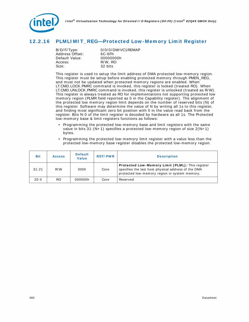
Intel® Virtualization Technology for Directed I/O Registers (D0:F0) (Intel® 82Q45 GMCH Only)
480 Datasheet
12.2.16 PLMLIMIT_REG—Protected Low-Memory Limit Register
B/D/F/Type: 0/0/0/DMIVC1REMAPAddress Offset: 6C-6FhDefault Value: 00000000hAccess: R/W, ROSize: 32 bits
This register is used to setup the limit address of DMA protected low-memory region. This register must be setup before enabling protected memory through PMEN_REG, and must not be updated when protected memory regions are enabled. When LT.CMD.LOCK.PMRC command is invoked, this register is locked (treated RO). When LT.CMD.UNLOCK.PMRC command is invoked, this register is unlocked (treated as R/W). This register is always treated as RO for implementations not supporting protected low memory region (PLMR field reported as 0 in the Capability register). The alignment of the protected low memory region limit depends on the number of reserved bits (N) of this register. Software may determine the value of N by writing all 1s to this register, and finding most significant zero bit position with 0 in the value read back from the register. Bits N:0 of the limit register is decoded by hardware as all 1s. The Protected low-memory base & limit registers functions as follows:
• Programming the protected low-memory base and limit registers with the same value in bits 31:(N+1) specifies a protected low-memory region of size 2(N+1) bytes.
• Programming the protected low-memory limit register with a value less than the protected low-memory base register disables the protected low-memory region.
Bit AccessDefault Value
RST/PWR Description
31:21 R/W 000h CoreProtected Low-Memory Limit (PLML): This register specifies the last host physical address of the DMA protected low-memory region in system memory.
20:0 RO 000000h Core Reserved

Datasheet 481
Intel® Virtualization Technology for Directed I/O Registers (D0:F0) (Intel® 82Q45 GMCH Only)
12.2.17 PHMBASE_REG—Protected High-Memory Base Register
B/D/F/Type: 0/0/0/DMIVC1REMAPAddress Offset: 70-77hDefault Value: 0000000000000000hAccess: R/W, ROSize: 64 bits
This register is used to setup the base address of DMA protected high-memory region. This register must be setup before enabling protected memory through PMEN_REG, and must not be updated when protected memory regions are enabled. When LT.CMD.LOCK.PMRC command is invoked, this register is locked (treated RO). When LT.CMD.UNLOCK.PMRC command is invoked, this register is unlocked (treated as R/W). This register is always treated as RO for implementations not supporting protected high memory region (PHMR field reported as 0 in the Capability register). The alignment of the protected high memory region base depends on the number of reserved bits (N) of this register. Software may determine the value of N by writing all 1s to this register, and finding most significant zero bit position below host address width (HAW) in the value read back from the register. Bits N:0 of the limit register is decoded by hardware as all 0s.
Bit AccessDefault Value
RST/PWR Description
63:21 R/W000000000
00hCore
Protected High-Memory Base (PHMB): This field specifies the base of size aligned, protected memory region in system memory. Hardware may not utilize bits 63:HAW, where HAW is the host address width. The protected high-memory region has a minimum size of 2 MB and must be size aligned.
20:0 RO 000000h Core Reserved

Intel® Virtualization Technology for Directed I/O Registers (D0:F0) (Intel® 82Q45 GMCH Only)
482 Datasheet
12.2.18 PHMLIMIT_REG—Protected High-Memory Limit Register
B/D/F/Type: 0/0/0/DMIVC1REMAPAddress Offset: 78-7FhDefault Value: 0000000000000000hAccess: RO, R/WSize: 64 bits
This register is used to setup the limit address of DMA protected high-memory region. This register must be setup before enabling protected memory through PMEN_REG, and must not be updated when protected memory regions are enabled. When LT.CMD.LOCK.PMRC command is invoked, this register is locked (treated RO). When LT.CMD.UNLOCK.PMRC command is invoked, this register is unlocked (treated as R/W). This register is always treated as RO for implementations not supporting protected high memory region (PHMR field reported as 0 in the Capability register). The alignment of the protected high memory region limit depends on the number of reserved bits (N) of this register. Software may determine the value of N by writing all 1s to this register, and finding most significant zero bit position below host address width (HAW) in the value read back from the register. Bits N:0 of the limit register is decoded by hardware as all 1s. The protected high-memory base and limit registers functions as follows:
• Programming the protected low-memory base and limit registers with the same value in bits HAW:(N+1) specifies a protected low-memory region of size 2(N+1) bytes.
• Programming the protected high-memory limit register with a value less than the protected high-memory base register disables the protected high-memory region.
Bit AccessDefault Value
RST/PWR Description
63:21 R/W000000000
00hCore
Protected High-Memory Limit (PHML): This field specifies the last host physical address of the DMA protected high-memory region in system memory. Hardware may not use bits 63:HAW, where HAW is the host address width.
20:0 RO 000000h Core Reserved
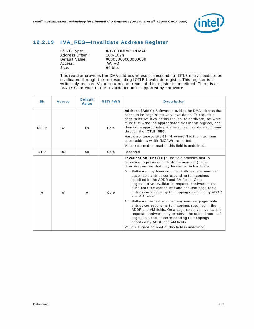
Datasheet 483
Intel® Virtualization Technology for Directed I/O Registers (D0:F0) (Intel® 82Q45 GMCH Only)
12.2.19 IVA_REG—Invalidate Address Register
B/D/F/Type: 0/0/0/DMIVC1REMAPAddress Offset: 100-107hDefault Value: 0000000000000000hAccess: W, ROSize: 64 bits
This register provides the DMA address whose corresponding IOTLB entry needs to be invalidated through the corresponding IOTLB Invalidate register. This register is a write-only register. Value returned on reads of this register is undefined. There is an IVA_REG for each IOTLB Invalidation unit supported by hardware.
Bit AccessDefault Value
RST/PWR Description
63:12 W 0s Core
Address (Addr): Software provides the DMA address that needs to be page-selectively invalidated. To request a page-selective invalidation request to hardware, software must first write the appropriate fields in this register, and then issue appropriate page-selective invalidate command through the IOTLB_REG.Hardware ignores bits 63: N, where N is the maximum guest address width (MGAW) supported. Value returned on read of this field is undefined.
11:7 RO 0s Core Reserved
6 W 0 Core
Invalidation Hint (IH): The field provides hint to hardware to preserve or flush the non-leaf (page-directory) entries that may be cached in hardware.0 = Software may have modified both leaf and non-leaf
page-table entries corresponding to mappings specified in the ADDR and AM fields. On a pageselective invalidation request, hardware must flush both the cached leaf and non-leaf page-table entries corresponding to mappings specified by ADDR and AM fields.
1 = Software has not modified any non-leaf page-table entries corresponding to mappings specified in the ADDR and AM fields. On a page-selective invalidation request, hardware may preserve the cached non-leaf page-table entries corresponding to mappings specified by ADDR and AM fields.
Value returned on read of this field is undefined.

Intel® Virtualization Technology for Directed I/O Registers (D0:F0) (Intel® 82Q45 GMCH Only)
484 Datasheet
5:0 W 0s Core
Address Mask (AM): The value in this field specifies the number of low order bits of the ADDR field that must be masked for the invalidation operation. Mask field enables software to request invalidation of contiguous mappings for size-aligned regions. For example: Mask Value ADDR bits masked Pages invalidated. Mask Value Addr bits masked Pg inval 0 Nil 1 1 12 2 2 13:12 4 3 14:12 8 4 15:12 16 5 16:12 32 6 17:12 64 7 18:12 128 8 19:12 256Hardware implementations report the maximum supported mask value through the Capability register. Value returned on read of this field is undefined.
Bit AccessDefault Value
RST/PWR Description

Datasheet 485
Intel® Virtualization Technology for Directed I/O Registers (D0:F0) (Intel® 82Q45 GMCH Only)
12.2.20 IOTLB_REG—IOTLB Invalidate Register
B/D/F/Type: 0/0/0/DMIVC1REMAPAddress Offset: 108-10FhDefault Value: 0000000000000000hAccess: R/W, ROSize: 64 bits
This register is used to control page-table entry caching. The act of writing the upper byte of the IOTLB_REG with IVT field set causes the hardware to perform the IOTLB invalidation. There is an IOTLB_REG for each IOTLB Invalidation unit supported by hardware.
Bit AccessDefault Value
RST/PWR Description
63 R/W 0 Core
Invalidate IOTLB (IVT): Software requests IOTLB invalidation by setting this field. Software must also set the requested invalidation granularity by programming the IIRG field. Hardware clears the IVT field to indicate the invalidation request is complete. Hardware also indicates the granularity at which the invalidation operation was performed through the IAIG field. Software must not submit another invalidation request through this register while the IVT field is set, nor update the associated Invalidate Address register.Software must not submit IOTLB invalidation requests through any of the IOTLB invalidation units when there is a context-cache invalidation request pending at this DMA-remapping hardware unit.When more than one IOTLB invalidation units are supported by a DMA-remapping hardware unit, software may submit IOTLB invalidation request through any of the currently free units while there are pending requests on other units.Hardware implementations reporting write-buffer flushing requirement (RWBF=1 in Capability register) must implicitly perform a write buffer flushing before reporting invalidation complete to software through the IVT field.

Intel® Virtualization Technology for Directed I/O Registers (D0:F0) (Intel® 82Q45 GMCH Only)
486 Datasheet
62:60 R/W 0s Core
IOTLB Invalidation Request Granularity (IIRG): When requesting hardware to invalidate the IOTLB (by setting the IVT field), software writes the requested invalidation granularity through this IIRG field.000 = Reserved.001 = Global invalidation request.010 = Domain-selective invalidation request. The target
domain-ID must be specified in the DID field.011 = Domain-page-selective invalidation request. The
target address, mask and invalidation hint must be specified in the Invalidate Address register, and the domain-ID must be provided in the DID field.
100–111 =Reserved.Hardware implementations may process an invalidation request by performing invalidation at a coarser granularity than requested. Hardware indicates completion of the invalidation request by clearing the IVT field. At this time, the granularity at which actual invalidation was performed is reported through the IAIG field.
59:57 RO 0s Core
IOTLB Actual Invalidation Granularity (IAIG): Hardware reports the granularity at which an invalidation request was processed through this field at the time of reporting invalidation completion (by clearing the IVT field).000 = Reserved. This indicates hardware detected an
incorrect invalidation request and ignored the request. Examples of incorrect invalidation requests include detecting an unsupported address mask value in Invalidate Address register for page-selective invalidation requests.
001 = Global Invalidation performed. This could be in response to a global, domain-selective, domain-page-selective, or device-page-selective invalidation request.
010 = Domain-selective invalidation performed using the domain-ID specified by software in the DID field. This could be in response to a domain-selective, domain-page-selective, or device-page-selective invalidation request.
011 = Domain-page-selective invalidation performed using the address, mask and hint specified by software in the Invalidate Address register and domain-ID specified in DID field. This can be in response to a domain-page-selective or device-page-selective invalidation request.
100 – 111 =Reserved.
56:50 RO 00h Core Reserved
Bit AccessDefault Value
RST/PWR Description

Datasheet 487
Intel® Virtualization Technology for Directed I/O Registers (D0:F0) (Intel® 82Q45 GMCH Only)
49 R/W 000000h Core
Drain Reads (DR): This field is ignored by hardware if the DRD field is reported as clear in the Capability register. When DRD field is reported as set in the Capability register, the following encodings are supported for this field:0 = Hardware may complete the IOTLB invalidation
without draining any translated DMA reads that are queued in the root-complex and yet to be processed.
1 = Hardware must drain all/relevant translated DMA reads that are queued in the root-complex before indicating IOTLB invalidation completion to software.
A DMA read request to system memory is defined as drained when root-complex has finished fetching all of its read response data from memory.
48 R/W 00h Core
Drain Writes (DW): This field is ignored by hardware if the DWD field is reported as clear in the Capability register.When DWD field is reported as set in the Capability register, the following encodings are supported for this field:0 = Hardware may complete the IOTLB invalidation
without draining any translated DMA writes that are queued in the root-complex for processing.
1 = Hardware must drain all/relevant translated DMA writes that are queued in the root-complex before indicating IOTLB invalidation completion to software.
A DMA write request to system memory is defined as drained when the effects of the write is visible to processor accesses to all addresses targeted by the DMA write.
47:32 R/W 0000h Core
Domain-ID (DID): This field indicates the id of the domain whose IOTLB entries needs to be selectively invalidated. This field must be programmed by software for domain-selective, domainpage-selective and device-page-selective invalidation requests.The Capability register reports the domain-ID width supported by hardware. Software must ensure that the value written to this field is within this limit.Hardware may ignore and not implement bits 47:(32+N) where N is the supported domain-ID width reported in the capability register.
31:0 RO 00000000h Core Reserved
Bit AccessDefault Value
RST/PWR Description

Intel® Virtualization Technology for Directed I/O Registers (D0:F0) (Intel® 82Q45 GMCH Only)
488 Datasheet
12.2.21 FRCD_REG—Fault Recording Registers
B/D/F/Type: 0/0/0/DMIVC1REMAPAddress Offset: 200-20FhDefault Value: 00000000000000000000000000000000hAccess: RO, RO/P, R/WC/PSize: 128 bits
This registers is used to record DMA-remapping fault information when primary fault logging is active. Hardware reports the number and location of fault recording registers through the Capability register. This register is relevant only for primary fault logging. These registers are sticky and can be cleared only through powergood reset or via software clearing the RW1C fields by writing a 1.
Bit AccessDefault Value
RST/PWR Description
127 R/WC/P 0s Core
Fault (F): Hardware sets this field to indicate a fault is logged in this Fault Recording register. The F field is set by hardware after the details of the fault is recorded in the PADDR, SID, FR and T fields.When this field is set, hardware may collapse additional faults from the same requestor (SID).Software writes the value read from this field to clear it.
126 RO/P 0s Core
Type (T): Type of the faulted DMA request.0 = DMA write1 = DMA read requestThis field is relevant only when the F field is set.
125:124 RO 0s Core
Address Type (AT): This field captures the AT field from the faulted DMA request. Hardware implementations not supporting Device- IOTLBs (DI field Clear in Extended Capability register) treat this field as Reserved.When supported, this field is valid only when the F field is Set, and when the fault reason (FR) indicates one of the DMA-remapping fault conditions.
NOTE: This field is reserved as this feature is not supported.
123:104 RO 0s Core Reserved
103:96 RO/P 0s CoreFault Reason (FR): Reason for the fault. Appendix B enumerates the various translation fault reason encodings.This field is relevant only when the F field is set.
95:80 RO 0s Core Reserved
79:64 RO/P 0s CoreSource Identifier (SID): Requester-ID of the faulted DMA request. This field is relevant only when the F field is set.
63:12 RO/P 0s Core
Fault Info (FI): This field contains the address (page-granular) in the faulted DMA request. Hardware may treat bits 63: N as reserved (0), where N is the maximum guest address width (MGAW) supported.This field is relevant only when the F field is set.
11:0 RO 0s Core Reserved

Datasheet 489
Intel® Virtualization Technology for Directed I/O Registers (D0:F0) (Intel® 82Q45 GMCH Only)
12.3 GFXVTBAR
Table 28. GFXVTBAR Register Address Map
Address Offset
Register Symbol
Register NameDefault Value
Access
0–3h VER_REG Version Register 00000010h RO
8–Fh CAP_REG Capability Register00C0000020230272h
RO
10–17h ECAP_REG Extended Capability Register0000000000001000h
RO
18–1Bh GCMD_REG Global Command Register 00000000h WO, RO
1C–1Fh GSTS_REG Global Status Register 00000000h RO
20–27h RTADDR_REG Root-Entry Table Address Register0000000000000000h
RO, R/W
28–2Fh CCMD_REG Context Command Register0800000000000000h
R/W, RO, WO
34–37h FSTS_REG Fault Status Register 00000000hR/WC/P, RO/P, RO
38–3Bh FECTL_REG Fault Event Control Register 80000000h RO, R/W
3C–3Fh FEDATA_REG Fault Event Data Register 00000000h RO, R/W
40–43h FEADDR_REG Fault Event Address Register 00000000h R/W, RO
44–47h FEUADDR_REG Fault Event Upper Address Register 00000000h RO
58–5Fh AFLOG_REG Advanced Fault Log Register0000000000000000h
RO
64–67h PMEN_REG Protected Memory Enable Register 00000000h R/W, RO
68–6Bh PLMBASE_REGProtected Low Memory Base Register
00000000h RO, R/W
6C–6Fh PLMLIMIT_REGProtected Low Memory Limit Register
00000000h R/W, RO
70–77h PHMBASE_REGProtected High Memory Base Register
0000000000000000h
RO, R/W
78–7Fh PHMLIMIT_REGProtected High Memory Limit Register
0000000000000000h
RO, R/W
100–107h IVA_REG Invalidate Address Register0000000000000000h
WO, RO
108–10Fh IOTLB_REG IOTLB Invalidate Register0200000000000000h
R/W, RO
200–20Fh FRCD_REG Fault Recording Registers
000000000000001000000000000
00000h
RO/P, R/WC/P, RO

Intel® Virtualization Technology for Directed I/O Registers (D0:F0) (Intel® 82Q45 GMCH Only)
490 Datasheet
12.3.1 VER_REG—Version Register
B/D/F/Type: 0/2/0/GFXVTBARAddress Offset: 0-3hDefault Value: 00000010hAccess: ROSize: 32 bits
This register reports the architecture version supported. Backward compatibility for the architecture is maintained with new revision numbers, allowing software to load DMA-remapping drivers written for prior architecture versions.
12.3.2 CAP_REG—Capability Register
B/D/F/Type: 0/2/0/GFXVTBARAddress Offset: 8-FhDefault Value: 00C0000020630272hAccess: ROSize: 64 bits
This register reports general translation hardware capabilities.
Bit AccessDefault Value
RST/PWR Description
31:8 RO 000000h Core Reserved
7:4 RO 1h CoreMajor Version number (MAX): This field indicates supported architecture version.
3:0 RO 0h CoreMinor Version number (MIN): This field indicates supported architecture minor version.
Bit AccessDefault Value
RST/PWR Description
63:56 RO 00h Core Reserved
55 RO 1h Core
DMA Read Draining (DRD):0 = As part of IOTLB invalidations, hardware does not
support draining of translated DMA read requests queued within the root complex
1 = As part of IOTLB invalidations, hardware supports draining of translated DMA read requests queued within the root complex
54 RO 1h Core
DMA Write Draining (DWD): 0 = On IOTLB invalidations, hardware does not support
draining of translated DMA writes queued within the root complex.
0 = On IOTLB invalidations, hardware supports draining of translated DMA writes queued within the root complex.
53:48 RO 00h Core
Maximum Address Mask Value (MAMV): The value in this field indicates the maximum supported value for the Address Mask (AM) field in the Invalidation Address (IVA_REG) register.
NOTE: This field is reserved as this feature is not supported.

Datasheet 491
Intel® Virtualization Technology for Directed I/O Registers (D0:F0) (Intel® 82Q45 GMCH Only)
47:40 RO 00h Core
Number of Faultrecording Registers (NFR): This field indicates a value of N-1, where N is the number of fault recording registers supported by hardware.Implementations must support at least one fault recording register (NFR = 0) for each DMAremapping hardware unit in the platform.The maximum number of fault recording registers per DMA-remapping hardware unit is 256.
39 RO 0b Core
Page-Selective Invalidation Support (PSI): 0 = Hardware does not support page-selective IOTLB
invalidations.1 = Hardware supports page-selective IOTLB invalidations.
The MAMV field indicates the maximum number of contiguous translations that may be invalidated in a single request.
NOTE: This field is reserved as this feature is not supported.
38 RO 0b Core Reserved
37:34 RO 0h Core
Super-Page support (SPS): This field indicates the super page sizes supported by hardware.A value of 1 in any of these bits indicates the corresponding super-page size is supported. The super-page sizes corresponding to various bit positions within this field are:0 = 21-bit offset to page frame1 = 30-bit offset to page frame2 = 39-bit offset to page frame3 = 48-bit offset to page frame
33:24 RO 020h Core
Fault-recording Register offset (FRO): This field specifies the location to the first fault recording register relative to the register base address of this DMA-remapping hardware unit.If the register base address is X, and the value reported in this field is Y, the address for the first fault recording register is calculated as X+(16*Y).
23 RO 0h Core
Isochrony (ISOCH): 0 = Remapping hardware unit has no critical isochronous
requesters in its scope.1 = Remapping hardware unit has one or more critical
isochronous requesters in its scope. To ensure isochronous performance, software must ensure invalidation operations do not impact active DMA streams from such requesters. This implies, when isochronous DMA is active, software performs page selective invalidations (and not coarser invalidations)
NOTE: This field is reserved as this feature is not supported.
Bit AccessDefault Value
RST/PWR Description

Intel® Virtualization Technology for Directed I/O Registers (D0:F0) (Intel® 82Q45 GMCH Only)
492 Datasheet
22 RO 1b Core
Zero Length Read (ZLR): 0 = Remapping hardware unit blocks (and treats as fault)
zero length DMA read requests to write-only pages.1 = Remapping hardware unit supports zero length DMA
read requests to write-only pages.
21:16 RO 23h Core
Maximum Guest Address Width (MGAW): This field indicates the maximum DMA virtual addressability supported by remapping hardware.The Maximum Guest Address Width (MGAW) is computed as (N+1), where N is the value reported in this field. For example, a hardware implementation supporting 48-bit MGAW reports a value of 47 (101111b) in this field.If the value in this field is X, DMA requests to addresses above 2(x+1)-1 are always blocked by hardware.Guest addressability for a given DMA request is limited to the minimum of the value reported through this field and the adjusted guest address width of the corresponding page-table structure. (Adjusted guest address widths supported by hardware are reported through the SAGAW field).
15:13 RO 0h Core Reserved
12:8 RO 02h Core
Supported adjusted guest address width (SAGAW): This 5-bit field indicates the supported adjusted guest address widths (which in turn represents the levels of page-table walks) supported by the hardware implementation.A value of 1 in any of these bits indicates the corresponding adjusted guest address width is supported. The adjusted guest address widths corresponding to various bit positions within this field are:0 = 30-bit AGAW (2-level page table)1 = 39-bit AGAW (3-level page table)2 = 48-bit AGAW (4-level page table)3 = 57-bit AGAW (5-level page table)4 = 64-bit AGAW (6-level page table)Software must ensure that the adjusted guest address width used to setup the page tables is one of the supported guest address widths reported in this field.
Bit AccessDefault Value
RST/PWR Description

Datasheet 493
Intel® Virtualization Technology for Directed I/O Registers (D0:F0) (Intel® 82Q45 GMCH Only)
7 RO 0h Core
Caching Mode (CM): 0 = Hardware does not cache not present and erroneous
entries in the context-cache and IOTLB. Invalidations are not required for modifications to individual not present or invalid entries. However, any modifications that result in decreasing the effective permissions or partial permission increases require invalidations for them to be effective.
1 = Hardware may cache not present and erroneous mappings in the context-cache or IOTLB. Any software updates to the DMA-remapping structures (including updates to not-present or erroneous entries) require explicit invalidation.
Hardware implementations are recommended to support operation corresponding to CM=0.
6 RO 1h Core
Protected High-Memory Region (PHMR): 0 = Protected high-memory region not supported.1 = Protected high-memory region is supported.
DMA-remapping hardware implementations on Intel TXT platforms supporting main memory above 4 GB are required to support protected high-memory region.
5 RO 1h Core
Protected Low-Memory Region (PLMR): 0 = Protected low-memory region not supported.1 = Protected low-memory region is supported.DMA-remapping hardware implementations on Intel TXT platforms are required to support protected low-memory region.
4 RO 1h Core
Required Write-Buffer Flushing (RWBF): 0 = No write-buffer flushing needed to ensure changes to
memory-resident structures are visible to hardware.1 = Software must explicitly flush the write buffers
(through the Global Command register) to ensure updates made to memory-resident DMA-remapping structures are visible to hardware.
3 RO 0h Core
Advanced Fault Logging (AFL): 0 = Advanced fault logging through memory-resident fault
log not supported. Only primary fault logging is supported.
1 = Advanced fault logging is supported.
Bit AccessDefault Value
RST/PWR Description

Intel® Virtualization Technology for Directed I/O Registers (D0:F0) (Intel® 82Q45 GMCH Only)
494 Datasheet
2:0 RO 2h Core
Number of domains supported (ND): 000 =Hardware supports 4-bit domain-IDs with support
for up to 16 domains.
001 =Hardware supports 6-bit domain-IDs with support for up to 64 domains.
010 =Hardware supports 8-bit domain-IDs with support for up to 256 domains.
011 =Hardware supports 10-bit domain-IDs with support for up to 1024 domains.
100 =Hardware supports 12-bit domain-IDs with support for up to 4K domains.
100 =Hardware supports 14-bit domain-IDs with support for up to 16K domains.
110 =Hardware supports 16-bit domain-IDs with support for up to 64K domains.
111 =Reserved.
Bit AccessDefault Value
RST/PWR Description

Datasheet 495
Intel® Virtualization Technology for Directed I/O Registers (D0:F0) (Intel® 82Q45 GMCH Only)
12.3.3 ECAP_REG—Extended Capability Register
B/D/F/Type: 0/2/0/GFXVTBARAddress Offset: 10-17hDefault Value: 0000000000001000hAccess: ROSize: 64 bits
the register reports DMA-remapping hardware extended capabilities.
Bit AccessDefault Value
RST/PWR Description
63:24 RO 00000000h Core Reserved
23:20 RO 0h Core
Maximum Handle Mask Value (MHMV): The value in this field indicates the maximum supported value for the Handle Mask (HM) field in the interrupt entry cache invalidation descriptor (iec_inv_dsc).This field is valid only when the IR field is reported as Set.
NOTE: This field is reserved as this feature is not supported.
19:18 RO 00b Core Reserved
17:8 RO 010h Core
Invalidation Unit Offset (IVO): This field specifies the location to the firstIOTLB invalidation unit relative to the registerbase address of this DMA-remapping hardwareunit.If the register base address is X, and the valuereported in this field is Y, the address for thefirst IOTLB invalidation unit is calculated asX+(16*Y).If N is the value reported in NIU field, theaddress for the last IOTLB invalidation unit iscalculated as X+(16*Y)+(16*N).
7 RO 0b Core
Snoop Control (SC): 0 = Hardware does not support 1-setting of the SNP field
in the page-table entries.1 = Hardware supports the 1-setting of the SNP field in the
page-table entries.
NOTE: This field is reserved as this feature is not supported.
6 RO 0b Core
Pass Through (PT): 0 = Hardware does not support pass through translation
type in context entries.1 = Hardware supports pass-through translation type in
context entries.
NOTE: This field is reserved as this feature is not supported.

Intel® Virtualization Technology for Directed I/O Registers (D0:F0) (Intel® 82Q45 GMCH Only)
496 Datasheet
5 RO 0b Core
Caching Hints (CH): 0 = Hardware does not support IOTLB caching hints (ALH
and EH fields in context-entries are treated as reserved).
1 = Hardware supports IOLTB caching hints through the ALH and EH fields in context-entries.
NOTE: This field is reserved as this feature is not supported.
4 RO 0b Core
Extended Interrupt Mode (EIM): 0 = Hardware supports only 8-bit APICIDs (Legacy
Interrupt Mode) on Intel®64 and IA-32 platforms and 16-bit APIC-IDs on ItaniumTM platforms.
1 = Hardware supports Extended Interrupt Mode (32-bit APIC-IDs) on Intel®64 platforms. This field is valid only when the IR field is reported as Set.
NOTE: This field is reserved as this feature is not supported.
3 RO 0b Core
Interrupt Remapping Support (IR): 0 = Hardware does not support interrupt remapping.1 = Hardware supports interrupt remapping.Implementations reporting this field as Set must also support Queued Invalidation (QI = 1b).
NOTE: This field is reserved as this feature is not supported.
2 RO 0b Core
Device IOTLB Support (DI): 0 = Hardware does not support device-IOTLBs.1 = Hardware supports Device-IOTLBs.Implementations reporting this field as Set must also support Queued Invalidation (QI = 1b).
NOTE: This field is reserved as this feature is not supported.
1 RO 0b Core
Queued Invalidation Support (QI): 0 = Hardware does not support queued invalidations.1 = Hardware supports queued invalidations.
NOTE: This field is reserved as this feature is not supported.
0 RO 0b Core
Coherency (C): 0 = Indicates hardware accesses to root, context and
page-table structures are not coherent (non-snooped).1 = Indicates hardware accesses to root, context and
page-table structures are coherent (snooped).Hardware writes to the advanced fault log is required to be coherent.
Bit AccessDefault Value
RST/PWR Description

Datasheet 497
Intel® Virtualization Technology for Directed I/O Registers (D0:F0) (Intel® 82Q45 GMCH Only)
12.3.4 GCMD_REG—Global Command Register
B/D/F/Type: 0/2/0/GFXVTBARAddress Offset: 18-1BhDefault Value: 00000000hAccess: WO, ROSize: 32 bits
This register is used to control DMA-remapping hardware. If multiple control fields in this register need to be modified, software must serialize through multiple accesses to this register.
Bit AccessDefault Value
RST/PWR Description
31 WO 0 Core
Translation Enable (TE): Software writes to this field to request hardware to enable/disable DMA-remapping hardware.0 = Disable DMA-remapping hardware1 = Enable DMA-remapping hardwareHardware reports the status of the translation enable
operation through the TES field in the Global Statusregister.Before enabling (or re-enabling) DMA-remappinghardware through this field, software must:• Setup the DMA-remapping structures in memory• Flush the write buffers (through WBF field), if write
buffer flushing is reported as required.• Set the root-entry table pointer in hardware (through
SRTP field).• Perform global invalidation of the context-cache and
global invalidation of IOTLB• If advanced fault logging supported, setup fault log
pointer (through SFL field) and enable advanced fault logging (through EAFL field).
There may be active DMA requests in the platform when software updates this field. Hardware must enable or disable remapping logic only at deterministic transaction boundaries, so that any in-flight transaction is either subject to remapping or not at all.Hardware implementations supporting DMA draining must drain any in-flight translated DMA read/write requests queued within the root complex before completing the translation enable command and reflecting the status of the command through the TES field in the GSTS_REG.Value returned on read of this field is undefined.

Intel® Virtualization Technology for Directed I/O Registers (D0:F0) (Intel® 82Q45 GMCH Only)
498 Datasheet
30 WO 0 Core
Set Root Table Pointer (SRTP): Software sets this field to set/update the root-entry table pointer used by hardware. The root-entry table pointer is specified through the Root-entry Table Address register.Hardware reports the status of the root table pointer set operation through the RTPS field in the Global Status register.The root table pointer set operation must be performed before enabling or re-enabling (after disabling) DMA-remapping hardware.After a root table pointer set operation, software must globally invalidate the context cache followed by global invalidate of IOTLB. This is required to ensure hardware uses only the remapping structures referenced by the new root table pointer, and not any stale cached entries.While DMA-remapping hardware is active, software may update the root table pointer through this field. However, to ensure valid in-flight DMA requests are deterministically remapped, software must ensure that the structures referenced by the new root table pointer are programmed to provide the same remapping results as the structures referenced by the previous root table pointer.Clearing this bit has no effect. Value returned on read of this field is undefined.
29 RO 0 Core
Set Fault Log (SFL): This field is valid only in implementations supporting advanced fault logging. If advanced fault logging is not supported, writes to this field are ignored.Software sets this field to request hardware to set/update the fault-log pointer used by hardware. The fault-log pointer is specified through Advanced Fault Log register.Hardware reports the status of the fault log set operation through the FLS field in the Global Status register. The fault log pointer must be set before enabling advanced fault logging (through EAFL field). Once advanced fault logging is enabled, the fault log pointer may be updated through this field while DMA-remapping hardware is active.Clearing this bit has no effect. Value returned on read of this field is undefined.
Bit AccessDefault Value
RST/PWR Description

Datasheet 499
Intel® Virtualization Technology for Directed I/O Registers (D0:F0) (Intel® 82Q45 GMCH Only)
28 RO 0 Core
Enable Advanced Fault Logging (EAFL): This field is valid only in implementations supporting advanced fault logging. If advanced fault logging is not supported, writes to this field are ignored.Software writes to this field to request hardware to enable or disable advanced fault logging.0 = Disable advanced fault logging. In this case,
translation faults are reported through the Fault Recording registers.
1 = Enable use of memory-resident 4 KB fault log. When enabled, translation faults are recorded in the memory-resident log. The fault log pointer must be set in hardware (through SFL field) before enabling advanced fault logging.
Hardware reports the status of the advanced fault logging enable operation through the AFLS field in the Global Status register.Value returned on read of this field is undefined.
27 WO 0 Core
Write Buffer Flush (WBF): This bit is valid only in implementations requiring write buffer flushing. If write buffer flushing is not required, writes to this field are ignored.Software sets this field to request hardware to flush the root-complex internal write buffers. This is done to ensure any updates to the memory-resident DMA-remap structures are not held in any internal write posting buffers.Hardware reports the status of the write buffer flushing operation through the WBFS field in the Global Status register.Clearing this bit has no effect. Value returned on read of this field is undefined.
26 RO 0b Core
Queued Invalidation Enable (QIE): This field is valid only for implementations supporting queued invalidations.Software writes to this field to enable or disable queued invalidations.0 = Disable queued invalidations.1 = Enable use of queued invalidations.Hardware reports the status of queued invalidation enable operation through QIES field in the Global Status register.The value returned on a read of this field is undefined.
NOTE: This field is reserved as this feature is not supported.
Bit AccessDefault Value
RST/PWR Description
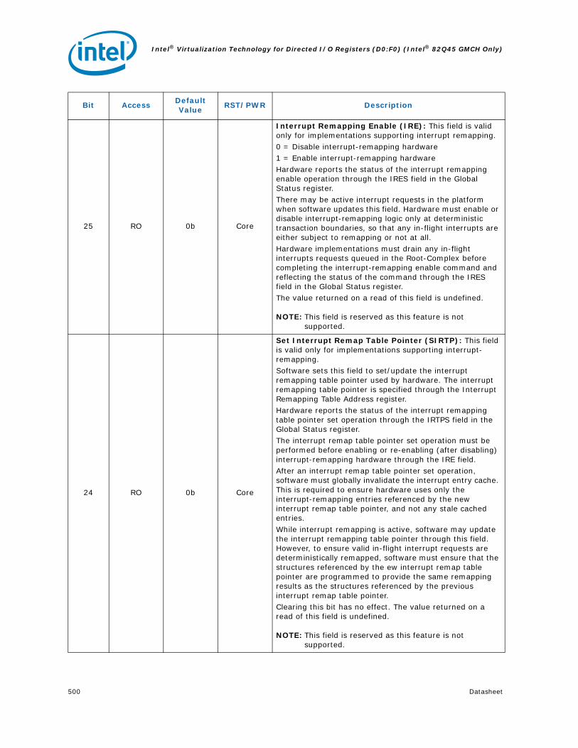
Intel® Virtualization Technology for Directed I/O Registers (D0:F0) (Intel® 82Q45 GMCH Only)
500 Datasheet
25 RO 0b Core
Interrupt Remapping Enable (IRE): This field is valid only for implementations supporting interrupt remapping.0 = Disable interrupt-remapping hardware1 = Enable interrupt-remapping hardwareHardware reports the status of the interrupt remapping enable operation through the IRES field in the Global Status register.There may be active interrupt requests in the platform when software updates this field. Hardware must enable or disable interrupt-remapping logic only at deterministic transaction boundaries, so that any in-flight interrupts are either subject to remapping or not at all.Hardware implementations must drain any in-flight interrupts requests queued in the Root-Complex before completing the interrupt-remapping enable command and reflecting the status of the command through the IRES field in the Global Status register.The value returned on a read of this field is undefined.
NOTE: This field is reserved as this feature is not supported.
24 RO 0b Core
Set Interrupt Remap Table Pointer (SIRTP): This field is valid only for implementations supporting interrupt-remapping.Software sets this field to set/update the interrupt remapping table pointer used by hardware. The interrupt remapping table pointer is specified through the Interrupt Remapping Table Address register.Hardware reports the status of the interrupt remapping table pointer set operation through the IRTPS field in the Global Status register.The interrupt remap table pointer set operation must be performed before enabling or re-enabling (after disabling) interrupt-remapping hardware through the IRE field.After an interrupt remap table pointer set operation, software must globally invalidate the interrupt entry cache. This is required to ensure hardware uses only the interrupt-remapping entries referenced by the new interrupt remap table pointer, and not any stale cached entries.While interrupt remapping is active, software may update the interrupt remapping table pointer through this field. However, to ensure valid in-flight interrupt requests are deterministically remapped, software must ensure that the structures referenced by the ew interrupt remap table pointer are programmed to provide the same remapping results as the structures referenced by the previous interrupt remap table pointer.Clearing this bit has no effect. The value returned on a read of this field is undefined.
NOTE: This field is reserved as this feature is not supported.
Bit AccessDefault Value
RST/PWR Description

Datasheet 501
Intel® Virtualization Technology for Directed I/O Registers (D0:F0) (Intel® 82Q45 GMCH Only)
23 RO 0b Core
Compatibility Format Interrupt (CFI): This field is valid only for Intel 64 implementations supporting interrupt-remapping.Software writes to this field to enable or disable Compatibility Format interrupts on Intel® 64 architectureplatforms. The value in this field is effective only when interrupt-remapping is enabled and Legacy Interrupt Mode is active.0 = Block Compatibility format interrupts.1 = Process Compatibility format interrupts as pass-
through (bypass interrupt remapping).Hardware reports the status of updating this field through the CFIS field in the Global Status register.The value returned on a read of this field is undefined.This field is not implemented on ItaniumTM
implementations.
NOTE: This field is reserved as this feature is not supported.
22:0 RO 0s Core Reserved
Bit AccessDefault Value
RST/PWR Description

Intel® Virtualization Technology for Directed I/O Registers (D0:F0) (Intel® 82Q45 GMCH Only)
502 Datasheet
12.3.5 GSTS_REG—Global Status Register
B/D/F/Type: 0/2/0/GFXVTBARAddress Offset: 1C-1FhDefault Value: 00000000hAccess: ROSize: 32 bits
This register reports general DMA-remapping hardware status.
Bit AccessDefault Value
RST/PWR Description
31 RO 0 Core
Translation Enable Status (TES): This field indicates the status of DMA-remapping hardware.0 = DMA-remapping hardware is not enabled1 = DMA-remapping hardware is enabled
30 RO 0 Core
Root Table Pointer Status (RTPS): This field indicates the status of the root- table pointer in hardware.This field is cleared by hardware when software sets the SRTP field in the Global Command register. This field is set by hardware when hardware finishes the set root-table pointer operation (by performing an implicit global invalidation of the context-cache and IOTLB, and setting/updating the root-table pointer in hardware with the value provided in the Root-Entry Table Address register).
29 RO 0 Core
Fault Log Status (FLS): This field is valid only in implementations supporting advanced fault logging.This field indicates the status of the fault-log pointer in hardware. This field is cleared by hardware when software sets the SFL field in the Global Command register. This field is set by hardware when hardware finishes the set fault-log pointer operation (by setting/updating the faultlog pointer in hardware with the value provided in the Advanced Fault Log register).
28 RO 0 Core
Advanced Fault Logging Status (AFLS): This field is valid only for implementations supporting advanced fault logging.This field indicates advanced fault logging status.0 = Advanced Fault Logging is not enabled1 = Advanced Fault Logging is enabled
27 RO 0 Core
Write Buffer Flush Status (WBFS): This bit is valid only in implementations requiring write buffer flushing.This field indicates the status of the write buffer flush operation. This field is set by hardware when software sets the WBF field in the Global Command register. This field is cleared by hardware when hardware finishes the write buffer flush operation.
26 RO 0 Core
Queued Invalidation Enable Status (QIES): This field indicates queued invalidation enable status.0 = queued invalidation is not enabled1 = queued invalidation is enabled

Datasheet 503
Intel® Virtualization Technology for Directed I/O Registers (D0:F0) (Intel® 82Q45 GMCH Only)
12.3.6 RTADDR_REG—Root-Entry Table Address Register
B/D/F/Type: 0/2/0/GFXVTBARAddress Offset: 20-27hDefault Value: 0000000000000000hAccess: RO, R/WSize: 64 bits
This register is used to setup location of root-entry table.
25 RO 0b Core
Interrupt Remapping Enable Status (IRES): This field indicates the status of Interrupt-remapping hardware.0 = Interrupt-remapping hardware is not enabled1 = Interrupt-remapping hardware is enabled
24 RO 0b Core
Interrupt Root Table Pointer Status (IRTPS): This field indicates the status of the interrupt remapping table pointer in hardware.This field is cleared by hardware when software sets the SIRTP field in the Global Command register.This field is Set by hardware when hardware completes the set interrupt remap table pointer operation using the value provided in the Interrupt Remapping Table Address register.
23 RO 0b Core
Compatibility Format Interrupt Status (CFIS): This field indicates the status of Compatibility format interrupts on Intel® 64 architecture implementations supporting interrupt-remapping. The value reported in this field is applicable only when interrupt-remapping is enabled and Legacy interrupt mode is active.0 = Compatibility format interrupts are blocked.1 = Compatibility format interrupts are processed as pass-
through (bypassing interrupt remapping).
22:0 RO 0s Core Reserved
Bit AccessDefault Value
RST/PWR Description
Bit AccessDefault Value
RST/PWR Description
63:36 RO 0s CoreRTA63:HAW (RTA_R): Made Read Only as hardware ignores bits 63:HAW.
35:12 R/W 0s Core
Root table address (RTA): This register points to base of page aligned, 4 KB-sized root-entry table in system memory. Hardware ignores bits 63:HAW, where HAW is the host address width.Software specifies the base address of the root-entry table through this register, and programs it in hardware through the SRTP field in the Global Command register.Reads of this register returns value that was last programmed to it.
11:0 RO 0s Core Reserved

Intel® Virtualization Technology for Directed I/O Registers (D0:F0) (Intel® 82Q45 GMCH Only)
504 Datasheet
12.3.7 CCMD_REG—Context Command Register
B/D/F/Type: 0/2/0/GFXVTBARAddress Offset: 28-2FhDefault Value: 0800000000000000hAccess: R/W, RO, WOSize: 64 bits
This register is used to manage context-entry cache. The act of writing the uppermost byte of the CCMD_REG with ICC field set causes the hardware to perform the context-cache invalidation.
Bit AccessDefault Value
RST/PWR Description
63 R/W 0 Core
Invalidate Context-entry Cache (ICC): Software requests invalidation of context-cache by setting this field. Software must also set the requested invalidation granularity by programming the CIRG field.Software must read back and check the ICC field to be clear to confirm the invalidation is complete. Software must not update this register when this field is set.
Hardware clears the ICC field to indicate the invalidation request is complete. Hardware also indicates the granularity at which the invalidation operation was performed through the CAIG field. Software must not submit another invalidation request through this register while the ICC field is set.Software must submit a context cache invalidation request through this field only when there are no invalidation requests pending at this DMA-remapping hardware unit. Since information from the context-cache may be used by hardware to tag IOTLB entries, software must perform domain-selective (or global) invalidation of IOTLB after the context cache invalidation has completed.Hardware implementations reporting write-buffer flushing requirement (RWBF=1 in Capability register) must implicitly perform a write buffer flushing before reporting invalidation complete to software through the ICC field.
62:61 R/W 00b Core
Context-cache Invalidation Request Granularity (CIRG): Software provides the requested invalidation granularity through this field when setting the ICC field.00 = Reserved.01 = Global Invalidation request.10 = Domain-selective invalidation request. The target
domain-ID must be specified in the DID field.11 = Device-selective invalidation request. The target
source-ID(s) must be specified through the SID and FM fields, and the domain-ID (that was programmed in the context-entry for these device(s)) must be provided in the DID field.
Hardware implementations may process an invalidation request by performing invalidation at a coarser granularity than requested. Hardware indicates completion of the invalidation request by clearing the ICC field. At this time, hardware also indicates the granularity at which the actual invalidation was performed through the CAIG field.
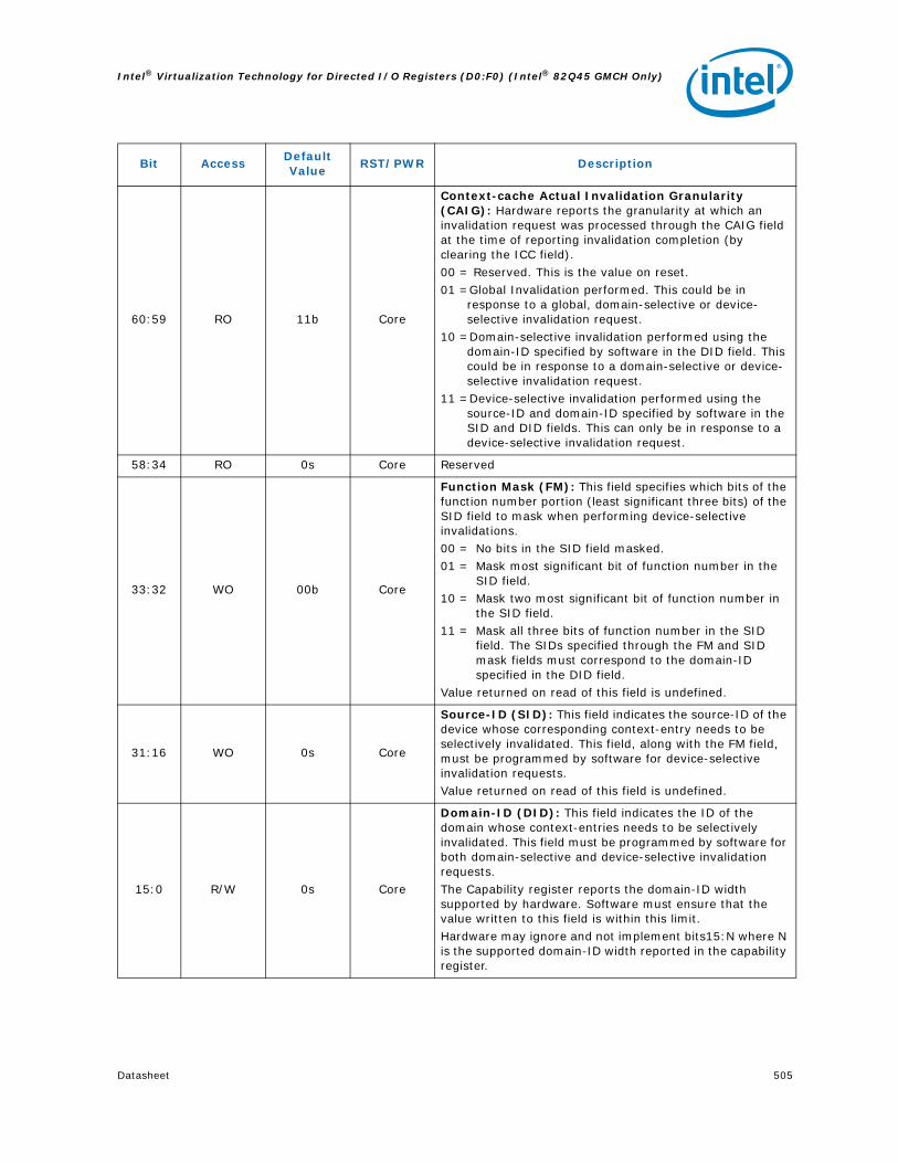
Datasheet 505
Intel® Virtualization Technology for Directed I/O Registers (D0:F0) (Intel® 82Q45 GMCH Only)
60:59 RO 11b Core
Context-cache Actual Invalidation Granularity (CAIG): Hardware reports the granularity at which an invalidation request was processed through the CAIG field at the time of reporting invalidation completion (by clearing the ICC field).00 = Reserved. This is the value on reset.01 =Global Invalidation performed. This could be in
response to a global, domain-selective or device-selective invalidation request.
10 =Domain-selective invalidation performed using the domain-ID specified by software in the DID field. This could be in response to a domain-selective or device-selective invalidation request.
11 =Device-selective invalidation performed using the source-ID and domain-ID specified by software in the SID and DID fields. This can only be in response to a device-selective invalidation request.
58:34 RO 0s Core Reserved
33:32 WO 00b Core
Function Mask (FM): This field specifies which bits of the function number portion (least significant three bits) of the SID field to mask when performing device-selective invalidations.00 = No bits in the SID field masked.01 = Mask most significant bit of function number in the
SID field.10 = Mask two most significant bit of function number in
the SID field.11 = Mask all three bits of function number in the SID
field. The SIDs specified through the FM and SID mask fields must correspond to the domain-ID specified in the DID field.
Value returned on read of this field is undefined.
31:16 WO 0s Core
Source-ID (SID): This field indicates the source-ID of the device whose corresponding context-entry needs to be selectively invalidated. This field, along with the FM field, must be programmed by software for device-selective invalidation requests.Value returned on read of this field is undefined.
15:0 R/W 0s Core
Domain-ID (DID): This field indicates the ID of the domain whose context-entries needs to be selectively invalidated. This field must be programmed by software for both domain-selective and device-selective invalidation requests.The Capability register reports the domain-ID width supported by hardware. Software must ensure that the value written to this field is within this limit.Hardware may ignore and not implement bits15:N where N is the supported domain-ID width reported in the capability register.
Bit AccessDefault Value
RST/PWR Description

Intel® Virtualization Technology for Directed I/O Registers (D0:F0) (Intel® 82Q45 GMCH Only)
506 Datasheet
12.3.8 FSTS_REG—Fault Status Register
B/D/F/Type: 0/2/0/GFXVTBARAddress Offset: 34-37hDefault Value: 00000000hAccess: RO, R/WC/P, RO/PSize: 32 bits
This register indicates the primary fault logging status.
Bit AccessDefault Value
RST/PWR Description
31:16 RO 0s Core Reserved
15:8 RO/P 0s Core
Fault Record Index (FRI): This field is valid only when the PPF field is set.The FRI field indicates the index (from base) of the fault recording register to which the first pending fault was recorded when the PPF field was set by hardware.Valid values for this field are from 0 to N, where N is the value reported through NFR field in the Capability register.
The value read from this field is undefined when the PPF field is clear.
7 RO 0b Core Reserved
6 RO 0b Core
Invalidation Time-out Error (ITE): Hardware detected a Device-IOTLB invalidation completion time-out. At this time, a fault event may be generated based on the programming of the Fault Event Control register.Hardware implementations not supporting Device-IOTLBs implement this bit as Reserved.
NOTE: This field is reserved as this feature is not supported.
5 RO 0b Core
Invalidation Completion Error (ICE): Hardware received an unexpected or invalid Device-IOTLB invalidation completion. This could be due to either an invalid ITag or invalid source-ID in an invalidation completion response. At this time, a fault event may be generated based on the programming of the Fault Event Control register.Hardware implementations not supporting Device-IOTLBs implement this bit as Reserved.
NOTE: This field is reserved as this feature is not supported.

Datasheet 507
Intel® Virtualization Technology for Directed I/O Registers (D0:F0) (Intel® 82Q45 GMCH Only)
4 RO 0b Core
Invalidation Queue Error (IQE): Hardware detected an error associated with the invalidation queue. This could be due to either a hardware error while fetching a descriptor from the invalidation queue, or hardware detecting an erroneous or invalid descriptor in the invalidation queue. At this time, a fault event may be generated based on the programming of the Fault Event Control register.Hardware implementations not supporting queued invalidations implement this bit as Reserved.
NOTE: This field is reserved as this feature is not supported.
3 RO 0b Core
Advanced Pending Fault (APF): When this field is Clear, hardware sets this field when the first fault record (at index 0) is written to a fault log. At this time, a fault event is generated based on the programming of the Fault Event Control register.Software writing 1 to this field clears it. Hardware implementations not supporting advanced fault logging implement this bit as Reserved.
NOTE: This field is reserved as this feature is not supported.
2 RO 0b Core
Advanced Fault Overflow (AFO): Hardware sets this field to indicate advanced fault log overflow condition. At this time, a fault event is generated based on the programming of the Fault Event Control register.Software writing 1 to this field clears it. Hardware implementations not supporting advanced fault logging implement this bit as Reserved.
NOTE: This field is reserved as this feature is not supported.
1 RO/P 0b Core
Primary Pending Fault (PPF): This field indicates if there are one or more pending faults logged in the fault recording registers. Hardware computes this field as the logical OR of Fault (F) fields across all the fault recording registers of this DMA-remap hardware unit.0 = No pending faults in any of the fault recording
registers1 = One or more fault recording registers has pending
faults. The FRI field is updated by hardware whenever the PPF field is set by hardware. Also, depending on the programming of fault event control register, a fault event is generated when hardware sets this bit.
0 R/WC/P 0b CorePrimary Fault Overflow (PFO): Hardware sets this bit to indicate overflow of fault recording registers. Software writing 1 clears this field.
Bit AccessDefault Value
RST/PWR Description
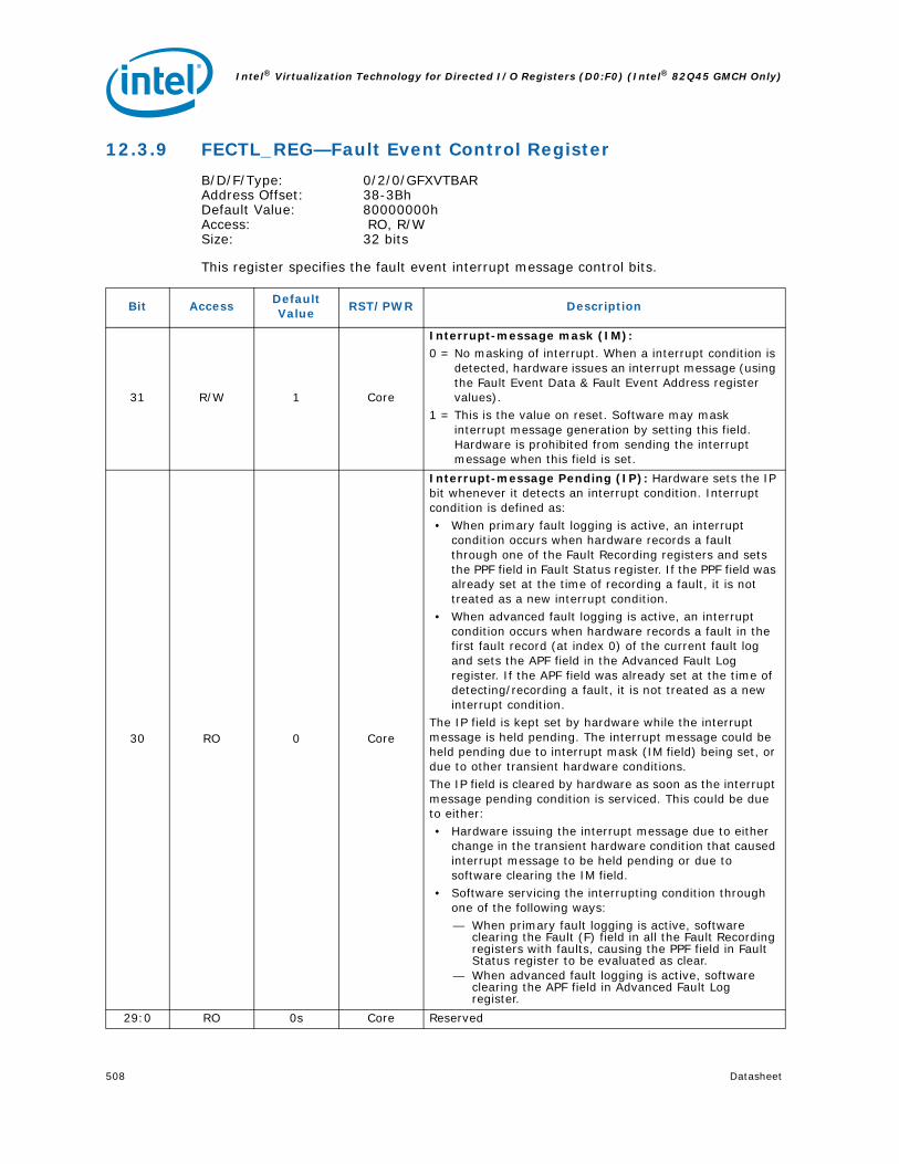
Intel® Virtualization Technology for Directed I/O Registers (D0:F0) (Intel® 82Q45 GMCH Only)
508 Datasheet
12.3.9 FECTL_REG—Fault Event Control Register
B/D/F/Type: 0/2/0/GFXVTBARAddress Offset: 38-3BhDefault Value: 80000000hAccess: RO, R/WSize: 32 bits
This register specifies the fault event interrupt message control bits.
Bit AccessDefault Value
RST/PWR Description
31 R/W 1 Core
Interrupt-message mask (IM): 0 = No masking of interrupt. When a interrupt condition is
detected, hardware issues an interrupt message (using the Fault Event Data & Fault Event Address register values).
1 = This is the value on reset. Software may mask interrupt message generation by setting this field. Hardware is prohibited from sending the interrupt message when this field is set.
30 RO 0 Core
Interrupt-message Pending (IP): Hardware sets the IP bit whenever it detects an interrupt condition. Interrupt condition is defined as:• When primary fault logging is active, an interrupt
condition occurs when hardware records a fault through one of the Fault Recording registers and sets the PPF field in Fault Status register. If the PPF field was already set at the time of recording a fault, it is not treated as a new interrupt condition.
• When advanced fault logging is active, an interrupt condition occurs when hardware records a fault in the first fault record (at index 0) of the current fault log and sets the APF field in the Advanced Fault Log register. If the APF field was already set at the time of detecting/recording a fault, it is not treated as a new interrupt condition.
The IP field is kept set by hardware while the interrupt message is held pending. The interrupt message could be held pending due to interrupt mask (IM field) being set, or due to other transient hardware conditions.The IP field is cleared by hardware as soon as the interrupt message pending condition is serviced. This could be due to either:• Hardware issuing the interrupt message due to either
change in the transient hardware condition that caused interrupt message to be held pending or due to software clearing the IM field.
• Software servicing the interrupting condition through one of the following ways:— When primary fault logging is active, software
clearing the Fault (F) field in all the Fault Recording registers with faults, causing the PPF field in Fault Status register to be evaluated as clear.
— When advanced fault logging is active, software clearing the APF field in Advanced Fault Log register.
29:0 RO 0s Core Reserved

Datasheet 509
Intel® Virtualization Technology for Directed I/O Registers (D0:F0) (Intel® 82Q45 GMCH Only)
12.3.10 FEDATA_REG—Fault Event Data Register
B/D/F/Type: 0/2/0/GFXVTBARAddress Offset: 3C-3FhDefault Value: 00000000hAccess: RO, R/WSize: 32 bits
This register specifies the interrupt message data.
12.3.11 FEADDR_REG—Fault Event Address Register
B/D/F/Type: 0/2/0/GFXVTBARAddress Offset: 40-43hDefault Value: 00000000hAccess: R/W, ROSize: 32 bits
This register specifies the interrupt message address.
Bit AccessDefault Value
RST/PWR Description
31:16 RO 0000h Core
Extended Interrupt Message Data (EID): This field is valid only for implementations supporting 32-bit MSI data fields.Hardware implementations supporting only 16-bit MSI data treats this field as read only (0).
15:0 R/W 0000h CoreInterrupt message data (ID): Data value in the fault-event interrupt message.
Bit AccessDefault Value
RST/PWR Description
31:2 R/W 00000000h CoreMessage address (MA): When fault events are enabled, the contents of this register specify the DWord aligned address (bits 31:2) for the MSI memory write transaction.
1:0 RO 0h Core Reserved

Intel® Virtualization Technology for Directed I/O Registers (D0:F0) (Intel® 82Q45 GMCH Only)
510 Datasheet
12.3.12 FEUADDR_REG—Fault Event Upper Address Register
B/D/F/Type: 0/2/0/GFXVTBARAddress Offset: 44-47hDefault Value: 00000000hAccess: ROSize: 32 bits
This register specifies the interrupt message address. For platforms supporting only interrupt messages in the 32-bit address range, this register is treated as read-only (0).
12.3.13 AFLOG_REG—Advanced Fault Log Register
B/D/F/Type: 0/2/0/GFXVTBARAddress Offset: 58-5FhDefault Value: 0000000000000000hAccess: ROSize: 64 bits
This register specifies the base address of memory-resident fault-log region. This register is treated as read only (0) for implementations not supporting advanced translation fault logging (AFL field reported as 0 in the Capability register). This register is sticky and can be cleared only through powergood reset or via software clearing the RW1C fields by writing a 1.
Bit AccessDefault Value
RST/PWR Description
31:0 RO 00000000h Core
Message upper address (MUA): This register need to be implemented only if hardware supports 64-bit message address. If implemented, the contents of this register specify the upper 32-bits of a 64- bit MSI write transaction.If hardware does not support 64-bit messages, the register is treated as read only (0).
Bit AccessDefault Value
RST/PWR Description
63:12 RO 0s Core
Fault Log Address (FLA): This field specifies the base of size-aligned fault-log region in system memory. Hardware may ignore bits 63: N, where N is the host addresswidth.Software specifies the base address and size of the fault log region through this register, and programs it in hardware through the SFL field in the Global Command register.When implemented, reads of this field returns value that was last programmed to it.
11:9 RO 0s Core
Fault Log Size (FLS): This field specifies the size of the fault log region pointed by the FLA field.The size of the fault log region is 2X * 4KB, where X is the value programmed in this register.When implemented, reads of this field returns value that was last programmed to it.
8:0 RO 0s Core Reserved

Datasheet 511
Intel® Virtualization Technology for Directed I/O Registers (D0:F0) (Intel® 82Q45 GMCH Only)
12.3.14 PMEN_REG—Protected Memory Enable Register
B/D/F/Type: 0/2/0/GFXVTBARAddress Offset: 64-67hDefault Value: 00000000hAccess: R/W, ROSize: 32 bits
This register is used to enable the DMA protected memory regions setup through the PLMBASE, PLMLIMT, PHMBASE, PHMLIMIT registers. When LT.CMD.LOCK.PMRC command is invoked, this register is locked (treated read-only). When the LT.CMD.UNLOCK.PMRC command is invoked, this register is unlocked (treated read/write). This register is always treated as read only (0) for implementations not supporting protected memory regions (PLMR and PHMR fields reported as 0 in the Capability register).
Bit AccessDefault Value
RST/PWR Description
31 R/W 0 Core
Enable Protected Memory Region (EPM): This field controls DMA accesses to the protected low-memory and protected high-memory regions.0 = DMA accesses to protected memory regions are
handled as follows:— If DMA-remapping hardware is not enabled, DMA
requests (including those to protected regions) are not blocked.
— If DMA-remapping hardware is enabled, DMA requests are translated per the programming of the DMA-remapping structures. Software may program the DMA-remapping structures to allow or block DMA to the protected memory regions.
1 = DMA accesses to protected memory regions are handled as follows:— If DMA-remapping hardware is not enabled, DMA to
protected memory regions are blocked. These DMA requests are not recorded or reported as DMA-remapping faults.
— If DMA-remapping hardware is enabled, hardware may or may not block DMA to the protected memory region(s). Software must not depend on hardware protection of the protected memory regions, and must ensure the DMA-remapping structures are properly programmed to not allow DMA to the protected memory regions.
Hardware reports the status of the protected memory enable/disable operation through the PRS field in this register.Hardware implementations supporting DMA draining must drain any in-flight translated DMA requests queued within the root complex before indicating the protected memory region as enabled through the PRS field.
30:1 RO 0s Core Reserved
0 RO 0s Core
Protected Region Status (PRS): This field indicates the status of protected memory region.0 = Protected memory region(s) not enabled.1 = Protected memory region(s) enabled.

Intel® Virtualization Technology for Directed I/O Registers (D0:F0) (Intel® 82Q45 GMCH Only)
512 Datasheet
12.3.15 PLMBASE_REG—Protected Low Memory Base Register
B/D/F/Type: 0/2/0/GFXVTBARAddress Offset: 68-6BhDefault Value: 00000000hAccess: RO, R/WSize: 32 bits
This register is used to setup the base address of DMA protected low-memory region. This register must be setup before enabling protected memory through PMEN_REG, and must not be updated when protected memory regions are enabled.
When LT.CMD.LOCK.PMRC command is invoked, this register is locked (treated RO).
When LT.CMD.UNLOCK.PMRC command is invoked, this register is unlocked (treated as R/W).
This register is always treated as RO for implementations not supporting protected low memory region (PLMR field reported as 0 in the Capability register). The alignment of the protected low memory region base depends on the number of reserved bits (N) of this register. Software may determine the value of N by writing all 1s to this register, and finding most significant zero bit position with 0 in the value read back from the register. Bits N:0 of this register is decoded by hardware as all 0s.
Bit AccessDefault Value
RST/PWR Description
31:21 R/W 000h CoreProtected Low-Memory Base (PLMB): This register specifies the base of protected low-memory region in system memory.
20:0 RO 000000h Core Reserved

Datasheet 513
Intel® Virtualization Technology for Directed I/O Registers (D0:F0) (Intel® 82Q45 GMCH Only)
12.3.16 PLMLIMIT_REG—Protected Low Memory Limit Register
B/D/F/Type: 0/2/0/GFXVTBARAddress Offset: 6C-6FhDefault Value: 00000000hAccess: R/W, ROSize: 32 bits
This register is used to setup the limit address of DMA protected low-memory region. This register must be setup before enabling protected memory through PMEN_REG, and must not be updated when protected memory regions are enabled.
When LT.CMD.LOCK.PMRC command is invoked, this register is locked (treated RO).
When LT.CMD.UNLOCK.PMRC command is invoked, this register is unlocked (treated as R/W).
This register is always treated as RO for implementations not supporting protected low memory region (PLMR field reported as 0 in the Capability register). The alignment of the protected low memory region limit depends on the number of reserved bits (N) of this register. Software may determine the value of N by writing all 1s to this register, and finding most significant zero bit position with 0 in the value read back from the register. Bits N:0 of the limit register is decoded by hardware as all 1s.
The Protected low-memory base & limit registers functions as follows:
• Programming the protected low-memory base and limit registers with the same value in bits 31:(N+1) specifies a protected low-memory region of size 2(N+1) bytes.
• Programming the protected low-memory limit register with a value less than the protected low-memory base register disables the protected low-memory region.
Bit AccessDefault Value
RST/PWR Description
31:21 R/W 000h CoreProtected Low-Memory Limit (PLML): This field specifies the last host physical address of the DMA protected low-memory region in system memory.
20:0 RO 000000h Core Reserved

Intel® Virtualization Technology for Directed I/O Registers (D0:F0) (Intel® 82Q45 GMCH Only)
514 Datasheet
12.3.17 PHMBASE_REG—Protected High Memory Base Register
B/D/F/Type: 0/2/0/GFXVTBARAddress Offset: 70-77hDefault Value: 0000000000000000hAccess: RO, R/WSize: 64 bits
This register is used to setup the base address of DMA protected high-memory region. This register must be setup before enabling protected memory through PMEN_REG, and must not be updated when protected memory regions are enabled.
When LT.CMD.LOCK.PMRC command is invoked, this register is locked (treated as RO).
When LT.CMD.UNLOCK.PMRC command is invoked, this register is unlocked (treated as R/W).
This register is always treated as RO for implementations not supporting protected high memory region (PHMR field reported as 0 in the Capability register). The alignment of the protected high memory region base depends on the number of reserved bits (N) of this register. Software may determine the value of N by writing all 1s to this register, and finding most significant zero bit position below host address width (HAW) in the value read back from the register. Bits N:0 of the limit register is decoded by hardware as all 0s.
Bit AccessDefault Value
RST/PWR Description
63:36 RO 0s Core Protected High-Memory Base (PHMB_R)
35:21 R/W 0s Core
Protected High-Memory Base (PHMB): This field specifies the base of size aligned, protected memory region in system memory. Hardware may ignore and not implement bits 63:HAW, where HAW is the host address width.
20:0 RO 0s Core Reserved

Datasheet 515
Intel® Virtualization Technology for Directed I/O Registers (D0:F0) (Intel® 82Q45 GMCH Only)
12.3.18 PHMLIMIT_REG—Protected High Memory Limit Register
B/D/F/Type: 0/2/0/GFXVTBARAddress Offset: 78-7FhDefault Value: 0000000000000000hAccess: RO, R/WSize: 64 bits
This register is used to setup the limit address of DMA protected high-memory region. This register must be setup before enabling protected memory through PMEN_REG, and must not be updated when protected memory regions are enabled.
When LT.CMD.LOCK.PMRC command is invoked, this register is locked (treated as RO).
When LT.CMD.UNLOCK.PMRC command is invoked, this register is unlocked (treated as R/W).
This register is always treated as RO for implementations not supporting protected high memory region (PHMR field reported as 0 in the Capability register). The alignment of the protected high memory region limit depends on the number of reserved bits (N) of this register. Software may determine the value of N by writing all 1s to this register, and finding most significant zero bit position below host address width (HAW) in the value read back from the register. Bits N:0 of the limit register is decoded by hardware as all 1s.
The protected high-memory base & limit registers functions as follows:
• Programming the protected low-memory base and limit registers with the same value in bits HAW:(N+1) specifies a protected low-memory region of size 2(N+1) bytes.
• Programming the protected high-memory limit register with a value less than the protected high-memory base register disables the protected high-memory region.
Bit AccessDefault Value
RST/PWR Description
63:36 RO 0s Core Protected High-Memory Limit (PHML_R):
35:21 R/W 0s Core
Protected High-Memory Limit (PHML): This register specifies the last host physical address of the DMA protected high-memory region in system memory. Hardware may ignore and not implement bits 63:HAW, where HAW is the host address width.
20:0 RO 0s Core Reserved

Intel® Virtualization Technology for Directed I/O Registers (D0:F0) (Intel® 82Q45 GMCH Only)
516 Datasheet
12.3.19 IVA_REG—Invalidate Address Register
B/D/F/Type: 0/2/0/GFXVTBARAddress Offset: 100-107hDefault Value: 0000000000000000hAccess: WO, ROSize: 64 bits
This register is used to provide the DMA address whose corresponding IOTLB entry needs to be invalidated through the IOTLB Invalidate register. This register is a write only register. The value returned on reads of this register is undefined. There is an IVA_REG for each IOTLB Invalidation unit supported by hardware.
Bit AccessDefault Value
RST/PWR Description
63:12 WO 0s Core
Address (ADDR): Software provides the DMA address that needs to be page-selectively invalidated. To request a page-selective invalidation request to hardware, software must first write the appropriate fields in this register, and then issue appropriate page-selective invalidate command through the IOTLB_REG. Hardware ignores bits 63:N, where N is the maximum guest address width (MGAW) supported. The value returned on read of this field is undefined.
11:7 RO 0s Core Reserved
6 WO 0 Core
Invalidation Hint (IH): The field provides hints to hardware to preserve or flush the non-leaf (page-directory) entries that may be cached in hardware.0 = Software may have modified both leaf and non-leaf
page-table entries corresponding to mappings specified in the ADDR and AM fields. On a pageselective invalidation request, hardware must flush both the cached leaf and non-leaf page-table entries corresponding to mappings specified by ADDR and AM fields.
1 = Software has not modified any non-leaf page-table entries corresponding to mappings specified in the ADDR and AM fields. On a page-selective invalidation request, hardware may preserve the cached non-leaf page-table entries corresponding to mappings specified by ADDR and AM fields.
Value returned on read of this field is undefined.

Datasheet 517
Intel® Virtualization Technology for Directed I/O Registers (D0:F0) (Intel® 82Q45 GMCH Only)
5:0 WO 0s Core
Address Mask (AM): The value in this field specifies the number of low-order bits of the ADDR field that must be masked for the invalidation operation. Mask field enables software to request invalidation of contiguous mappings for size-aligned regions. For example: Mask Value ADDR bits masked Pages invalidated 0 None 11 12 22 13 : 12 43 14 : 12 84 15 : 12 16...... ....... .......Hardware implementations report the maximum supported mask value through the Capability register. Value returned on read of this field is undefined.
Bit AccessDefault Value
RST/PWR Description

Intel® Virtualization Technology for Directed I/O Registers (D0:F0) (Intel® 82Q45 GMCH Only)
518 Datasheet
12.3.20 IOTLB_REG—IOTLB Invalidate Register
B/D/F/Type: 0/2/0/GFXVTBARAddress Offset: 108-10FhDefault Value: 0200000000000000hAccess: R/W, ROSize: 64 bits
This register is used to control page-table entry caching. The act of writing the upper byte of the IOTLB_REG with IVT field set causes the hardware to perform the IOTLB invalidation. There is an IOTLB_REG for each IOTLB Invalidation unit supported by hardware.
Bit AccessDefault Value
RST/PWR Description
63 R/W 0 Core
Invalidate IOTLB (IVT): Software requests IOTLB invalidation by setting this field. Software must also set the requested invalidation granularity by programming the IIRG field.Hardware clears the IVT field to indicate the invalidation request is complete. Hardware also indicates the granularity at which the invalidation operation was performed through the IAIG field. Software must not submit another invalidation request through this register while the IVT field is set, nor update the associated Invalidate Address register.Software must not submit IOTLB invalidation requests through any of the IOTLB invalidation units when there is a context-cache invalidation request pending at this DMA-remapping hardware unit.When more than one IOTLB invalidation units are supported by a DMA-remapping hardware unit, software may submit IOTLB invalidation request through any of the currently free units while there are pending requests on other units.Hardware implementations reporting write-buffer flushing requirement (RWBF=1 in Capability register) must implicitly perform a write buffer flushing before reporting invalidation complete to software through the IVT field.

Datasheet 519
Intel® Virtualization Technology for Directed I/O Registers (D0:F0) (Intel® 82Q45 GMCH Only)
62:60 R/W 0s Core
IOTLB Invalidation Request Granularity (IIRG): When requesting hardware to invalidate the IOTLB (by setting the IVT field), software writes the requested invalidation granularity through this IIRG field.000 = Reserved. Hardware ignores the invalidation
request and reports invalidation complete by clearing the IVT field and reporting 000 in the IAIG field.
001 = Global invalidation request.010 = Domain-selective invalidation request. The target
domain-ID must be specified in the DID field.011 = Domain-page-selective invalidation request. The
target address, mask and invalidation hint must be specified in the Invalidate Address register, and the domain-ID must be provided in the DID field.
100 = Device-page-selective invalidation request. The target address, mask and invalidation hint must be specified in the Invalidate Address register, the domain-ID must be provided in the DID field, and the device requestor-ID must be provided in SID field.
101 - 111 =Reserved. Hardware ignores the invalidation request and reports invalidation complete by clearing the IVT field and reporting 000 in the IAIG field.
Depending on the invalidation granularities supported by a hardware implementation, an invalidation request may be processed by performing invalidation at a coarser granularity. Hardware indicates completion of the invalidation request by clearing the IVT field. At this time, the granularity at which actual invalidation was performed is reported through the IAIG field.
Bit AccessDefault Value
RST/PWR Description

Intel® Virtualization Technology for Directed I/O Registers (D0:F0) (Intel® 82Q45 GMCH Only)
520 Datasheet
59:57 RO 1h Core
IOTLB Actual Invalidation Granularity (IAIG): Hardware reports the granularity at which an invalidation request was proceed through this field at the time of reporting invalidation completion (by clearing the IVT field).000 = Reserved. This indicates hardware detected an
incorrect invalidation request and hence ignored the request. Examples of incorrect invalidation requests include specifying a reserved value in the IIRG field or specifying an unsupported address mask value in IVA_REG for page-selective invalidation requests.
001 = Global Invalidation performed. This could be in response to a global, domain-selective, domain-page-selective, or device-page-selectiveinvalidation request.
010 = Domain-selective invalidation performed using the domain-ID specified by software in the DID field. This could be in response to a domain-selective, domain-page-selective, or device-page-selective invalidation request.
011 = Domain-page-selective invalidation performed using the address, mask and hint specified by software in the Invalidate Address register and domain-ID specified in DID field. This can be in response to a domain-page-selective or device-page-selective invalidation request.
100 = Device-page-selective invalidation performed using the address, mask and hint specified by software in the Invalidate Address register and device-ID specified in SID field. This can only be in response to a device-page-selective invalidation request.
101 - 111 =Reserved.
56:50 RO 0 Core Reserved
49 R/W 0 Core
Drain Reads (DR): This field is treated as reserved if the DRD field is reported as clear in the Capability register.0 = Hardware may complete the IOTLB invalidation
without draining any translated DMA reads that are queued in the root-complex and yet to be processed.
1 = Hardware must drain all/relevant translated DMA reads that are queued in the root-complex before indicating IOTLB invalidation completion to software. A DMA read request to system memory is defined as drained when root-complex has finished fetching all of its read response data from memory.
Bit AccessDefault Value
RST/PWR Description
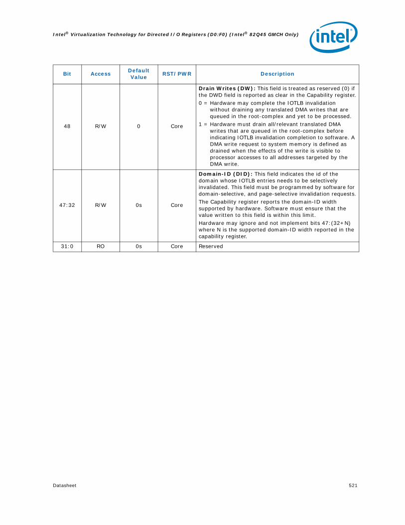
Datasheet 521
Intel® Virtualization Technology for Directed I/O Registers (D0:F0) (Intel® 82Q45 GMCH Only)
48 R/W 0 Core
Drain Writes (DW): This field is treated as reserved (0) if the DWD field is reported as clear in the Capability register.0 = Hardware may complete the IOTLB invalidation
without draining any translated DMA writes that are queued in the root-complex and yet to be processed.
1 = Hardware must drain all/relevant translated DMA writes that are queued in the root-complex before indicating IOTLB invalidation completion to software. A DMA write request to system memory is defined as drained when the effects of the write is visible to processor accesses to all addresses targeted by the DMA write.
47:32 R/W 0s Core
Domain-ID (DID): This field indicates the id of the domain whose IOTLB entries needs to be selectively invalidated. This field must be programmed by software for domain-selective, and page-selective invalidation requests.The Capability register reports the domain-ID width supported by hardware. Software must ensure that the value written to this field is within this limit.
Hardware may ignore and not implement bits 47:(32+N) where N is the supported domain-ID width reported in the capability register.
31:0 RO 0s Core Reserved
Bit AccessDefault Value
RST/PWR Description

Intel® Virtualization Technology for Directed I/O Registers (D0:F0) (Intel® 82Q45 GMCH Only)
522 Datasheet
12.3.21 FRCD_REG—Fault Recording Registers
B/D/F/Type: 0/2/0/GFXVTBARAddress Offset: 200-20FhDefault Value: 00000000000000100000000000000000hAccess: RO/P, RO, R/WC/PSize: 128 bits
This register is used to record DMA-remapping fault information when primary fault logging is active. Hardware reports the number and location of fault recording registers through the Capability register. This register is relevant only for primary fault logging. These registers are sticky and can be cleared only through powergood reset or via software clearing the RW1C fields by writing a 1.
Bit AccessDefault Value
RST/PWR Description
127 R/WC/P 0 Core
Fault (F): Hardware sets this field to indicate a fault is logged in this Fault Recording register. The F field is Set by hardware after the details of the fault is recorded in other fields.
When this field is set, hardware may collapse additional faults from the same source-ID (SID).Software writes the value read from this field to Clear it.
126 RO/P 0 Core
Type (T): Type of the faulted DMA request0 = DMA write1 = DMA read requestThis field is relevant only when the F field is set.
125:124 RO 00b Core
Address Type (AT): This field captures the AT field from the faulted DMA request.Hardware implementations not supporting Device-IOTLBs (DI field Clear in Extended Capability register) treat this field as Reserved.When supported, this field is valid only when the F field is set, and when the fault reason (FR) indicates one of the DMA-remapping fault conditions.
NOTE: This field is reserved as this feature is not supported.
123:104 RO 0s Core Reserved
103:96 RO/P 0s CoreFault Reason (FR): Reason for the fault. This field is relevant only when the F field is set.
95:80 RO 0s Core Reserved
79:64 RO/P 0010h CoreSource Identifier (SID): Requester-ID of the faulted DMA request.This field is relevant only when the F field is set.

Datasheet 523
Intel® Virtualization Technology for Directed I/O Registers (D0:F0) (Intel® 82Q45 GMCH Only)
§ §
63:36 RO/P 0s Core
Fault Info (FI): When the Fault Reason (FR) field indicates one of the DMA-remapping fault conditions, bits 63:12 of this field contains the page address in the faulted DMA request. Hardware treat bits 63:N as reserved (0), where N is the maximum guest address width (MGAW) supported.When the Fault Reason (FR) field indicates one of the interrupt-remapping fault conditions, bits 63:48 of this field indicate the interrupt_index computed for the faulted interrupt request, and bits 47:12 are cleared.This field is relevant only when the F field is Set.
35:32 RO/P 0h Core
Fault Info (FI): When the Fault Reason (FR) field indicates one of the DMA-remapping fault conditions, bits 63:12 of this field contains the page address in the faulted DMA request. Hardware treat bits 63:N as reserved (0), where N is the maximum guest address width (MGAW) supported.When the Fault Reason (FR) field indicates one of the interrupt-remapping fault conditions, bits 63:48 of this field indicate the interrupt_index computed for the faulted interrupt request, and bits 47:12 are cleared.This field is relevant only when the F field is Set.
31:12 RO/P 0s Core
Fault Info (FI): When the Fault Reason (FR) field indicates one of the DMA-remapping fault conditions, bits 63:12 of this field contains the page address in the faulted DMA request. Hardware treat bits 63:N as reserved (0), where N is the maximum guest address width (MGAW) supported.When the Fault Reason (FR) field indicates one of the interrupt-remapping fault conditions, bits 63:48 of this field indicate the interrupt_index computed for the faulted interrupt request, and bits 47:12 are cleared.This field is relevant only when the F field is Set.
11:0 RO 0s Core Reserved
Bit AccessDefault Value
RST/PWR Description

Intel® Virtualization Technology for Directed I/O Registers (D0:F0) (Intel® 82Q45 GMCH Only)
524 Datasheet

Datasheet 525
Functional Description
13 Functional Description
13.1 Host Interface
The (G)MCH supports the Intel® Core™2 Extreme processor QX9000 series, Intel® Core™2 Quad processor Q9000 series, and Intel® Core™2 Duo processor E8000 and E7000 series in the LGA775 Land Grid Array Package. The cache line size is 64 bytes. Source synchronous transfer is used for the address and data signals. The address signals are double pumped and a new address can be generated every other bus clock. At 200/267/333MHz bus clock the address signals run at 667MT/s. The data is quad pumped and an entire 64B cache line can be transferred in two bus clocks. At 200/266/333 MHz bus clock, the data signals run at 800/1066/1333 MT/s for a maximum bandwidth of 6.4/8.5/10.6 GB/s.
13.1.1 FSB IOQ Depth
The Scalable Bus supports up to 12 simultaneous outstanding transactions.
13.1.2 FSB OOQ Depth
The (G)MCH supports only one outstanding deferred transaction on the FSB.
13.1.3 FSB GTL+ Termination
The (G)MCH integrates GTL+ termination resistors on die.
13.1.4 FSB Dynamic Bus Inversion
The (G)MCH supports Dynamic Bus Inversion (DBI) when driving and when receiving data from the processor. DBI limits the number of data signals that are driven to a low voltage on each quad pumped data phase. This decreases the worst-case power consumption of the (G)MCH. FSB_DINVB_[3:0] indicate if the corresponding 16 bits of data are inverted on the bus for each quad pumped data phase:
Whenever the processor or the (G)MCH drives data, each 16-bit segment is analyzed. If more than 8 of the 16 signals would normally be driven low on the bus, the corresponding FSB_DINVB signal will be asserted, and the data will be inverted prior to being driven on the bus. Whenever the processor or the (G)MCH receives data, it monitors FSB_DINVB_[3:0] to determine if the corresponding data segment should be inverted.
FSB_DINVB_[3:0] Data Bits
FSB_DINVB_0 FSB_DB_[15:0]#
FSB_DINVB_1 FSB_DB_[31:16]#
FSB_DINVB_2 FSB_DB_[47:32]#
FSB_DINVB_3 FSB_DB_[63:48]#

Functional Description
526 Datasheet
13.1.5 APIC Cluster Mode Support
APIC Cluster mode support is required for backwards compatibility with existing software, including various operating systems.
The (G)MCH supports three types of interrupt re-direction:
• Physical
• Flat-Logical
• Clustered-Logical
If more than one xTPR register set in the arbitration pool has the same lowest value, or if all enabled xTPR Task Priority fields are 1111b, the xTPR register set referenced by the lowest value TPR_SEL[3:0] is the “winner”.
The “winning” xTPR register set provides the values to be substituted in the Aa[19:12]# and Aa[7:4]# fields of the FSB Interrupt Message Transaction driven by the (G)MCH.
Table 29. Host Interface 4X, 2X, and 1X Signal Groups
Signals Associated Clock or StrobeSignal Group
FSB_ADSB, FSB_BNRB, FSB_BPRIB, FSB_DEFERB, FSB_DBSYB, FSB_DRDYB, FSB_HITB, FSB_HITMB, FSB_LOCKB, FSB_RSB_[2:0], FSB_TRDYB, RSTINB
HPL_CLKINPHPL_CLKINN
1X
FSB_AB_[16:3], FSB_REQB_[4:0] FSB_ADSTBB_02X
FSB_AB_[35:17] FSB_ADSTBB_1
FSB_DB_[15:0], FSB_DINVB_0 FSB_DSTBPB_0, FSB_DSTBNB_0
4XFSB_DB_[31:16], FSB_DINVB_1 FSB_DSTBPB_1, FSB_DSTBNB_1
FSB_DB_[47:32], FSB_DINVB_2 FSB_DSTBPB_2, FSB_DSTBNB_2
FSB_DB_[63:48], FSB_DINVB_3 FSB_DSTBPB_3, FSB_DSTBNB_3

Datasheet 527
Functional Description
13.2 System Memory Controller
The (G)MCH system memory controller supports both DDR2 and DDR3 protocols with two independent 64 bit wide channels each accessing one or two DIMMs. The controller supports a maximum of two non-ECC DDR2 DIMMs or two un-buffered non-ECC DDR3 DIMMs per channel; thus, allowing up to four device ranks per channel. Intel® Fast Memory Access (FMA) supported.
Note: The 82G41 GMCH only supports 1 DIMM per channel. References to 2 DIMMs per channel only apply to the 82Q45, 82Q43, 82B43, 82G45, 82G43 GMCH and 82P45, 82P43 MCH. The 82G43 supports 1 or 2 DIMMs per channel depending upon part.
13.2.1 System Memory Organization Modes
The system memory controller supports two memory organization modes: Single Channel and Dual Channel.
13.2.1.1 Single Channel Mode
In this mode, all memory cycles are directed to a single channel.
Single channel mode is used when either Channel A or Channel B DIMMs are populated in any order, but not both.
13.2.1.2 Dual Channel Modes
13.2.1.2.1 Dual Channel Symmetric Mode
This mode provides maximum performance on real applications. Addresses are ping-ponged between the channels after each cache line (64 byte boundary). If there are two requests, and the second request is to an address on the opposite channel from the first, that request can be sent before data from the first request has returned. If two consecutive cache lines are requested, both may be retrieved simultaneously, since they are assured to be on opposite channels.
Dual channel symmetric mode is used when both Channel A and Channel B DIMMs are populated in any order with the total amount of memory in each channel being the same, but the DRAM device technology and width may vary from one channel to the other.
Table 30 is a sample dual channel symmetric memory configuration showing the rank organization.
Table 30. Sample System Memory Dual Channel Symmetric Organization Mode
RankChannel 0 Population
Cumulative Top Address in Channel 0
Channel 1 Population
Cumulative Top Address in Channel 1
Rank 3 0 MB 2560 MB 0 MB 2560 MB
Rank 2 256 MB 2560 MB 256 MB 2560 MB
Rank 1 512 MB 2048 MB 512 MB 2048 MB
Rank 0 512 MB 1024 MB 512 MB 1024 MB

Functional Description
528 Datasheet
13.2.1.2.2 Dual Channel Asymmetric Mode with Intel® Flex Memory Mode Enabled
In this addressing mode the lowest DRAM memory is mapped to dual channel operation and the top most DRAM memory is mapped to single channel operation. In this mode the system can run at one zone of dual channel mode and one zone of single channel mode simultaneously across the whole memory array.
This mode is used when Intel® Flex Memory Mode is enabled and both Channel A and Channel B DIMMs are populated in any order with the total amount of memory in each channel being different.
Table 31 is a sample dual channel asymmetric memory configuration showing the rank organization with Intel® Flex Memory Mode Enabled.
13.2.1.2.3 Dual Channel Asymmetric Mode with Intel® Flex Memory Mode Disabled (Stacked Mode)
In this addressing mode addresses start in channel 0 and stay there until the end of the highest rank in channel 0, and then addresses continue from the bottom of channel 1 to the top.
This mode is used when Intel® Flex Memory Mode is disabled and both Channel A and Channel B DIMMs are populated in any order with the total amount of memory in each channel being different.
Table 32 is a sample dual channel asymmetric memory configuration showing the rank organization with Intel® Flex Memory Mode Disabled.
Table 31. Sample System Memory Dual Channel Asymmetric Organization Mode with Intel® Flex Memory Mode Enabled
RankChannel 0 population
Cumulative top address in Channel 0
Channel 1 population
Cumulative top address in Channel 1
Rank 3 0 MB 2048 MB 0 MB 2304 MB
Rank 2 0 MB 2048 MB 256 MB 2304 MB
Rank 1 512 MB 2048 MB 512 MB 2048 MB
Rank 0 512 MB 1024 MB 512 MB 1024 MB
Table 32. Sample System Memory Dual Channel Asymmetric Organization Mode with Intel® Flex Memory Mode Disabled
RankChannel 0 population
Cumulative top address in Channel 0
Channel 1 population
Cumulative top address in Channel 1
Rank 3 0 MB 1280 MB 0 MB 2304 MB
Rank 2 256 MB 1280 MB 0 MB 2304 MB
Rank 1 512 MB 1024 MB 512 MB 2304 MB
Rank 0 512 MB 512 MB 512 MB 1792 MB

Datasheet 529
Functional Description
13.2.2 System Memory Technology Supported
The (G)MCH supports the following DDR2 and DDR3 Data Transfer Rates, DIMM Modules, and DRAM Device Technologies:
• DDR2 Data Transfer Rates: 667 (PC2-5300) and 800 (PC2-6400)
• DDR3 Data Transfer Rates: 800 (PC3-6400) and 1066 (PC3-8500)
• DDR2 DIMM Modules:
— Raw Card C - Single Sided x16 un-buffered non-ECC
— Raw Card D - Single Sided x8 un-buffered non-ECC
— Raw Card E - Double Sided x8 un-buffered non-ECC
• DDR3 DIMM Modules:
— Raw Card A - Single Sided x8 un-buffered non-ECC
— Raw Card B - Double Sided x8 un-buffered non-ECC
— Raw Card C - Single Sided x16 un-buffered non-ECC
— Raw Card F - Double Sided x16 un-buffered non-ECC
• DDR2 DRAM Device Technology: 512-Mb, 1-Gb, and 2-Gb
• DDR3 DRAM Device Technology: 512-Mb and 1-Gb
Table 33. Supported DIMM Module Configurations
Memory Type
Raw Card
Version
DIMM Capacity
DRAM Device
Technology
DRAM Organization
# of DRAM
Devices
# of Physical Device Ranks
# of Row/
Col Address
Bits
# of Banks Inside DRAM
Page Size
DDR2 667 and
800(see note)
C256MB 512Mb 32M X 16 4 1 13/10 4 8K
512MB 1Gb 64M X 16 4 1 13/10 8 8K
D512MB 512Mb 64M X 8 8 1 14/10 4 8K
1GB 1Gb 128M X 8 8 1 14/10 8 8K
E1GB 512Mb 64M X 8 16 2 14/10 4 8K
2GB 1Gb 128M X 8 16 2 14/10 8 8K
F512MB 512Mb 64M X 8 9 1 14/10 4 8K
1GB 1Gb 128M X 8 9 1 14/10 8 8K
G1GB 512Mb 64M X 8 18 2 14/10 4 8K
2GB 1Gb 128M X 8 18 2 14/10 8 8K
DDR3 800 and
1066
A512 MB 512Mb 64M X 8 8 1 13/10 8 8K
1 GB 1Gb 128M X 8 8 1 14/10 8 8K
B1 GB 512Mb 64M X 8 16 2 13/10 8 8K
2 GB 1Gb 128M X 8 16 2 14/10 8 8K
C256 MB 512Mb 32M X 16 4 1 12/10 8 8K
512 MB 1Gb 64M X 16 4 1 13/10 8 8K
F512 MB 512Mb 32M X 16 8 2 12/10 8 8K
1 GB 1Gb 64M X 16 8 2 13/10 8 8K

Functional Description
530 Datasheet
13.3 PCI Express*
See Section 1.2 for a list of PCI Express features, and the PCI Express Specification for further details.
This (G)MCH is part of a PCI Express root complex. This means it connects a host processor/memory subsystem to a PCI Express hierarchy. The control registers for this functionality are located in Device 1 and Device 6 configuration space and two Root Complex Register Blocks (RCRBs). The DMI RCRB contains registers for control of the ICH10/ICH7 attach ports.
13.3.1 PCI Express* Architecture
The PCI Express architecture is specified in layers. Compatibility with the PCI addressing model (a load-store architecture with a flat address space) is maintained to ensure that all existing applications and drivers operate unchanged. The PCI Express configuration uses standard mechanisms as defined in the PCI Plug-and-Play specification. The initial speed of 1.25 GHz (250 MHz internally) results in 2.5 Gb/s each direction which provides a 250 MB/s communications channel in each direction (500 MB/s total) that is close to twice the data rate of classic PCI per lane.
13.3.1.1 Transaction Layer
The upper layer of the PCI Express architecture is the Transaction Layer. The Transaction Layer’s primary responsibility is the assembly and disassembly of Transaction Layer Packets (TLPs). TLPs are used to communicate transactions, such as read and write, as well as certain types of events. The Transaction Layer also manages flow control of TLPs.
13.3.1.2 Data Link Layer
The middle layer in the PCI Express stack, the Data Link Layer, serves as an intermediate stage between the Transaction Layer and the Physical Layer. Responsibilities of Data Link Layer include link management, error detection, and error correction.
13.3.1.3 Physical Layer
The Physical Layer includes all circuitry for interface operation, including driver and input buffers, parallel-to-serial and serial-to-parallel conversion, PLL(s), and impedance matching circuitry.
13.3.2 PCI Express* on (G)MCH
The (G)MCH has two PCIe Gen 2.0 controllers to support 1x16 graphics or 2x8 graphics modes. To support 1x16 and 2x8 graphics the system should incorporate two graphics ports- Primary port and Secondary port. Each port is a 1x16 physical connector but 1x8 electrically.
Note: Not all of the above configurations are supported on all Intel 4 Series Chipset (G)MCH components. Refer to Table 1 in Chapter 1 for (G)MCH components supporting specific features.
On plugging a PCI Express Gen 2.0 1x16 PCIe graphics card into the primary port the transaction between the (G)MCH and the PCI Express graphics card will take place along all the 16 PCI Express lanes. When graphic cards are plugged into both the primary and secondary ports transaction between the (G)MCH and the graphics card

Datasheet 531
Functional Description
will take place along 8 of the PCI express lanes through each ports. This means that when two x16 graphics cards are plugged into both the slots, the (G)MCH will dynamically down sample and transaction takes place only through 8 lanes.
The PCI Express controllers on the (G)MCH has been designed to support ADD2 and MEC only the primary slot. When a ADD2 or MEC card is plugged into the secondary slot, the card will not function.
Table 34 shows the usage models supported on the (G)MCH for PCI Express graphics cards, ADD2 and ADD2+ cards.
NOTE: X indicates support available is N/A - Support not available.
Table 34. Supported Usage Models
Ports PCIe Graphics Card MEC ADD2
Primary SlotPCIex16 card in stand alonePCIe x8 card in dual graphics mode
X X
Secondary SlotPCIe x8 card in dual graphics modeNo support available with card only in secondary slot
N/A N/A

Functional Description
532 Datasheet
13.4 Integrated Graphics Device (Intel® 82Q45, 82Q43, 82B43, 82G45, 82G43 GMCH Only)
This section details the chipset integrated graphics engines (3D, 2D, and Video), 3D pipeline, and the respective capabilities.
The GMCH graphics device supports ten fully programmable execution cores, enabling greater performance than previous generation chipsets.
The GMCH internal graphics devices (IGD) contain several types of components. The major components in the IGD are the engines, planes, pipes, and ports. The GMCH has a 3D/2D Instruction Processing unit to control the 3D and 2D engines, respectively. The IGD’s 3D and 2D engines are fed with data through the memory controller. The outputs of the engines are surfaces sent to memory, which are then retrieved and processed by GMCH planes.
13.4.1 3D and Video Engines for Graphics Processing
The 3D graphics pipeline for the chipset has a deep pipelined architecture in which each stage can simultaneously operate on different primitives or on different portions of the same primitive. All the cores are fully programmable, increasing the versatility of the 3D Engine.
The 3D engine also has a number of performance and power-management enhancements, providing improved power/performance ratios over the IGD. These include:
• Execution Units increased to 10 from the previous 8 EUs
• Improved HDDVD hardware acceleration
• Graphics support for Intel Virtualization Technology DMA
• Graphics support for Intel TXT (82Q45/82Q43 GMCH Only)
• Intel HD Audio Playback AVC/VC1 decoding in hardware
Figure 10. GMCH Graphics Controller Block Diagram
Plane B
Cursor C
Sprite C
Plane C
Cursor B
Sprite B
Pipe C
Pipe B
Memory
MultiPLEXEr
CRT
SDVO B/C
VGA
Video Engine
2D Engine
3D Engine
Clipper
Strip & Fan/Setup
Alpha Blend/ Gamma/Panel
Fitter
Geometry Shader
Vertex Fetch/Vertex Shader
Windower/IZ
iHDMI
DP

Datasheet 533
Functional Description
13.4.1.1 3D Engine Execution Units (EUs)
The 3D processing hardware includes support for 2 more EUs over the previous generation. The EUs perform 128-bit wide execution per clock and are support SIMD8 instructions for vertex processing and SIMD16 instructions for pixel processing.
13.4.1.2 3D Pipeline
13.4.1.2.1 Vertex Fetch (VF) Stage
The VF stage performs one major function: executing 3DPRIMITIVE commands. Some enhancements have been included to better support legacy DirectX 3D APIs as well as OpenGL.
13.4.1.2.2 Vertex Shader (VS) Stage
The VS stage of the 3D pipeline is used to perform shading of vertices output by the VF function. The VS unit will, thus, produce an output vertex reference for every input vertex reference received from the VF unit, in the order received.
13.4.1.2.3 Geometry Shader (GS) Stage
The GS stage receives inputs from the previous VS stage. Compiled application-provided GS shader programs specify an algorithm to convert the vertices of an input object into some output primitives. For example, a GS shader may convert lines of a line strip into polygons representing a corresponding segment of a blade of grass centered on the line. Or it could use adjacency information to detect silhouette edges of triangles and output polygons extruding out from the those edges.
13.4.1.2.4 Clip Stage
The CLIP stage can be used to perform general processing on incoming 3D objects. However, it also includes specialized logic to perform a ClipTest function on incoming object. The Clip Test optimizes generalized 3D Clipping. The Clip unit examines the position of incoming vertices, and accepts/rejects 3D objects based on its Clip algorithm.
13.4.1.2.5 Strips and Fans Stage
The Strips and Fans (SF) stage of the 3D pipeline is responsible for performing setup operations required to rasterize 3D objects. The outputs from the SF stage to the Windower stage comprise of implementation-specific information required for the rasterization of objects and also supports clipping of primitives to some extent.
13.4.1.2.6 Windower/IZ (WIZ) Stage
The WIZ unit performs an early depth test, a major performance-optimization feature where failing pixels are removed; thus, eliminating unnecessary processing overhead.
The Windower uses the parameters provided by the SF unit in the object-specific rasterization algorithms. The WIZ unit rasterizes objects into the corresponding set of pixels.
The Windower is also capable of performing dithering, whereby the illusion of a higher resolution when using low-bpp channels in color buffers is possible. Color dithering tends to diffuse the sharp color bands seen on smooth-shaded objects.

Functional Description
534 Datasheet
13.4.2 Video Engine
The Video Engine handles the non-3D (media/video) applications. It includes support for VLD and MPEG2 decode in Hardware. The GMCH engine includes a number of encompassments over the previous generation capabilities, which have been listed above.
13.4.3 2D Engine
The GMCH contains BLT (Block Level Transfer) functionality and an extensive set of 2D instructions. To take advantage of the 3D drawing engine’s functionality, some BLT functions make use of the 3D renderer.
13.4.3.1 Chipset VGA Registers
The 2D registers are a combination of registers for the original Video Graphics Array (VGA) and others to support graphics modes that have color depths, resolutions, and hardware acceleration features that go beyond the original VGA standard.
13.4.3.2 Logical 128-Bit Fixed BLT and 256 Fill Engine
Use of this BLT engine accelerates the Graphical User Interface (GUI) of Microsoft Windows* operating systems. The 128-bit GMCH BLT Engine provides hardware acceleration of block transfers of pixel data for many common Windows operations. The term BLT refers to a block transfer of pixel data between memory locations. The BLT engine can be used for the following:
• Move rectangular blocks of data between memory locations
• Data Alignment
• Perform logical operations (raster ops)
The rectangular block of data does not change as it is transferred between memory locations. The allowable memory transfers are between: cacheable system memory and frame buffer memory, frame buffer memory and frame buffer memory, and within system memory. Data to be transferred can consist of regions of memory, patterns, or solid color fills. A pattern will always be 8x8 pixels wide and may be 8, 16, or 32 bits per pixel.
The BLT engine has the ability to expand monochrome data into a color depth of 8, 16, or 32 bits. BLTs can be either opaque or transparent. Opaque transfers move the data specified to the destination. Transparent transfers compare destination color to source color and write according to the mode of transparency selected.
Data is horizontally and vertically aligned at the destination. If the destination for the BLT overlaps with the source memory location, the GMCH can specify which area in memory to begin the BLT transfer. Hardware is included for all 256 raster operations (Source, Pattern, and Destination) defined by Microsoft, including transparent BLT.
The GMCH has instructions to invoke BLT and stretch BLT operations, permitting software to set up instruction buffers and use batch processing. The GMCH can perform hardware clipping during BLTs.

Datasheet 535
Functional Description
13.5 Display Interfaces (Intel® 82Q45, 82Q43, 82B43, 82G45, 82G43, 82G41 GMCH Only)
The GMCH has three display ports, one analog and two digital ports B and C. Each port can transmit data according to one or more protocols. The digital ports B and C can be configured to drive natively HDMI, DVI and Display Port or can be connected to an external device (SDVO) that converts one protocol to another. Examples of SDVO devices are TV encoders, external DACs, LVDS transmitters, HDMI transmitters, and TMDS transmitters. Each display port has control signals that may be used to control, configure and/or determine the capabilities of an external device.
The GMCH has one dedicated display port, the analog port. Digital ports B and C are multiplexed with the PCI Express Graphics (PEG) interface and are not available if an external PEG device is in use. The digital ports can also be configured to drive SDVO data. When a system uses a PEG connector, SDVO ports B and C can be used via an ADD2 (Advanced Digital Display 2) or MEC (Media Expansion Card).
• The GMCH’s analog port uses an integrated 350 MHz RAMDAC that can directly drive a standard progressive scan analog monitor up to a resolution of 2048x1536 pixels with 32-bit color at 75 Hz.
• The GMCH’s SDVO ports are each capable of driving a 400 MP pixel rate. Each port is capable of driving a digital display up to 2560x1600 @ 60Hz.
Integrated HDMI, DVI, and Display Port support multiplexed over PCI Express Graphics port for native connection to a compatible display.
13.5.1 Analog Display Port Characteristics
The analog display port provides a RGB signal output along with a HSYNC and VSYNC signal. There is an associated DDC signal pair that is implemented using GPIO pins dedicated to the analog port. The intended target device is for a CRT based monitor with a VGA connector. Display devices such as LCD panels with analog inputs may work satisfactory but no functionality added to the signals to enhance that capability.
Table 35. Analog Port Characteristics
Signal Port Characteristic Support
RGB
Voltage Range 0.7 V p-p only
Monitor Sense Analog Compare
Analog Copy Protection No
Sync on Green No
HSYNCVSYNC
Voltage 2.5 V
Enable/Disable Port control
Polarity adjust VGA or port control
Composite Sync Support No
Special Flat Panel Sync No
Stereo Sync No
DDCVoltage Externally buffered to 5V
Control Through GPIO interface

Functional Description
536 Datasheet
13.5.1.1 Integrated RAMDAC
The display function contains a RAM-based Digital-to-Analog Converter (RAMDAC) that transforms the digital data from the graphics and video subsystems to analog data for the CRT monitor. GMCH’s integrated 350 MHz RAMDAC supports resolutions up to 2048 x 1536 @ 75 Hz. Three 8-bit DACs provide the R, G, and B signals to the monitor.
13.5.1.2 Sync Signals
HSYNC and VSYNC signals are digital and conform to TTL signal levels at the connector. Since these levels cannot be generated internal to the device, external level shifting buffers are required. These signals can be polarity adjusted and individually disabled in one of the two possible states. The sync signals should power up disabled in the high state. No composite sync or special flat panel sync support will be included.
13.5.1.3 VESA/VGA Mode
VESA/VGA mode provides compatibility for pre-existing software that set the display mode using the VGA CRTC registers. Timings are generated based on the VGA register values and the timing generator registers are not used.
13.5.1.4 DDC (Display Data Channel)
DDC is a standard defined by VESA. Its purpose is to allow communication between the host system and display. Both configuration and control information can be exchanged allowing plug- and-play systems to be realized. Support for DDC 1 and DDC 2 is implemented. The GMCH uses the CRT_DDC_CLK and CRT_DDC_DATA signals to communicate with the analog monitor. The GMCH will generate these signals at 2.5 V. External pull-up resistors and level shifting circuitry should be implemented on the board.
The GMCH implements a hardware GMBus controller that can be used to control these signals allowing for transactions speeds up to 400 kHz.
13.5.2 Digital Display Interface
The GMCH can drive HDMI, DVI, and Display Port natively. The digital ports B and/or C can be configured to drive HDMI, DVI, and Display Port. The digital ports are multiplexed on to the PEG interface.
13.5.2.1 High Definition Multimedia Interface (Intel® 82G45, 82G43, 82G41, 82B43 GMCH Only)
The High-Definition Multimedia Interface (HDMI) is provided for transmitting uncompressed digital audio and video signals from DVD players, set-top boxes, and other audiovisual sources to television sets, projectors, and other video displays. It can carry high-quality multi-channel audio data and all standard and high-definition consumer electronics video formats.
HDMI display interface connecting the GMCH and display devices uses transition minimized differential signaling (TMDS) to carry audiovisual information through the same HDMI cable.
HDMI includes three separate communications channels: TMDS, DDC, and the optional CEC (consumer electronics control). As shown in Figure 11, the HDMI cable carries four differential pairs that make up the TMDS data and clock channels. These channels are used to carry video, audio and auxiliary data. In addition, HDMI carries a VESA Display data channel (DDC). The DDC channel is used by an HDMI Source to determine the capabilities and characteristics of the Sink.
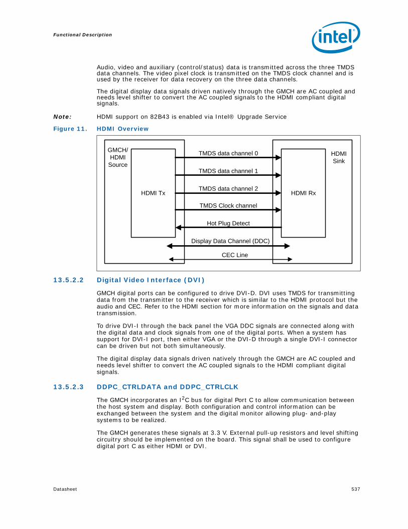
Datasheet 537
Functional Description
Audio, video and auxiliary (control/status) data is transmitted across the three TMDS data channels. The video pixel clock is transmitted on the TMDS clock channel and is used by the receiver for data recovery on the three data channels.
The digital display data signals driven natively through the GMCH are AC coupled and needs level shifter to convert the AC coupled signals to the HDMI compliant digital signals.
Note: HDMI support on 82B43 is enabled via Intel® Upgrade Service
13.5.2.2 Digital Video Interface (DVI)
GMCH digital ports can be configured to drive DVI-D. DVI uses TMDS for transmitting data from the transmitter to the receiver which is similar to the HDMI protocol but the audio and CEC. Refer to the HDMI section for more information on the signals and data transmission.
To drive DVI-I through the back panel the VGA DDC signals are connected along with the digital data and clock signals from one of the digital ports. When a system has support for DVI-I port, then either VGA or the DVI-D through a single DVI-I connector can be driven but not both simultaneously.
The digital display data signals driven natively through the GMCH are AC coupled and needs level shifter to convert the AC coupled signals to the HDMI compliant digital signals.
13.5.2.3 DDPC_CTRLDATA and DDPC_CTRLCLK
The GMCH incorporates an I2C bus for digital Port C to allow communication between the host system and display. Both configuration and control information can be exchanged between the system and the digital monitor allowing plug- and-play systems to be realized.
The GMCH generates these signals at 3.3 V. External pull-up resistors and level shifting circuitry should be implemented on the board. This signal shall be used to configure digital port C as either HDMI or DVI.
Figure 11. HDMI Overview
TMDS data channel 0
TMDS data channel 1
TMDS data channel 2
TMDS Clock channel
Hot Plug Detect
Display Data Channel (DDC)
HDMI Tx HDMI Rx
CEC Line
HDMISink
GMCH/HDMI
Source

Functional Description
538 Datasheet
13.5.2.4 Display Port
Display Port is a digital communication interface that utilizes differential signalling to achieve a high bandwidth bus interface designed to support connections between PCs and monitors, projectors, and TV displays. Display port is also suitable for display connections between consumer electronics devices such as high definition optical disc players, set top boxes, and TV displays.
A Display Port consists of a Main Link, Auxiliary channel, and a Hot Plug Detect signal. The Main Link is a uni-directional, high-bandwidth, and low latency channel used for transport of isochronous data streams such as uncompressed video and audio. The Auxiliary Channel (AUX CH) is a half-duplex bi-directional channel used for link management and device control. The Hot Plug Detect (HPD) signal serves as an interrupt request for the sink device.
13.5.2.5 Auxiliary Channel (AUX CH)
The Auxiliary channel consists of an AC-coupled, bi-directional differential pair, providing a data rate of 1 Mbps. It is used for link management and device control (that is, for transmitting control and status information).
AUX CH is multiplexed to the PCI Express Rx lanes.
13.5.2.6 PEG Mapping of digital display signals
Table 36 shows the PEG mapping of HDMI(DVI), Display Port, and SDVO signals.
Figure 12. Display Port Overview
Main Link(Isochronous Streams)
Display Port Tx
Display Port Rx
Sink DeviceSource Device
Aux Channel(Link/Device Management)
Hot Plug Detect(Interrupt Request)

Datasheet 539
Functional Description
Table 36. (G)MCH PCI Express TX/RX Mapping of Supported Display Technologies
PCI Express Differential pair
lanes
PCI Express Differential pair lanes with lane
reversal
DisplayPort Signals
HDMI/DVI Signals SDVO signals Description
PEG_TXP_7 PEG_TXP_8 DPC_LANE3 TMDSC_CLK1 SDVOC_CLK DisplayPort Cor HDMI CorSDVO C
PEG_TXN_7 PEG_TXN_8 DPC_LANE3# TMDSC_CLK1# SDVOC_CLK#
PEG_TXP_6 PEG_TXP_9 DPC_LANE2 TMDSC_DATA0 SDVOC_BLUE
PEG_TXN_6 PEG_TXN_9 DPC_LANE2# TMDSC_DATA0# SDVOC_BLUE#
PEG_TXP_5 PEG_TXP_10 DPC_LANE1 TMDSC_DATA1 SDVOC_GREEN
PEG_TXN_5 PEG_TXN_10 DPC_LANE1# TMDSC_DATA1# SDVOC_GREEN#
PEG_TXP_4 PEG_TXP_11 DPC_LANE0 TMDSC_DATA2 SDVOC_RED
PEG_TXN_4 PEG_TXN_11 DPC_LANE0# TMDSC_DATA2# SDVOC_RED#
PEG_TXP_3 PEG_TXP_12 DPB_LANE3 TMDSB_CLK2 SDVOB_CLK DisplayPort Bor HDMI BorSDVO B
PEG_TXN_3 PEG_TXN_12 DPB_LANE3# TMDSB_CLK2# SDVOB_CLK#
PEG_TXP_2 PEG_TXP_13 DPB_LANE2 TMDSB_DATA0 SDVO_BLUE
PEG_TXN_2 PEG_TXN_13 DPB_LANE2# TMDSB_DATA0# SDVO_BLUE#
PEG_TXP_1 PEG_TXP_14 DPB_LANE1 TMDSB_DATA1 SDVOB_GREEN
PEG_TXN_1 PEG_TXN_14 DPB_LANE1# TMDSB_DATA1# SDVOB_GREEN#
PEG_TXP_0 PEG_TXP_15 DPB_LANE0 TMDSB_DATA2 SDVOB_RED
PEG_TXN_0 PEG_TXN_15 DPB_LANE0# TMDSB_DATA2# SDVOB_RED#
PEG_RXP_7 PEG_RXP_8 DPC_HPD TMDSC_HPD HPD for DP C and HDMI C
PEG_RXN_7 PEG_RXN_8
PEG_RXP_6 PEG_RXP_9 DPC_AUX AUX CH for Display port C
PEG_RXN_6 PEG_RXN_9 DPC_AUX#
PEG_RXP_5 PEG_RXP_10 SDVOC_INT
PEG_RXN_5 PEG_RXN_10 SDVOC_INTB
PEG_RXP_4 PEG_RXP_11
PEG_RXN_4 PEG_RXN_11
PEG_RXP_3 PEG_RXP_12 DPC_HPD HDMIB_HPD HPD for DP B and HDMI B
PEG_RXN_3 PEG_RXN_12
PEG_RXP_2 PEG_RXP_13 DPB_AUX SDVO_FLDSTALLSDVO PEG_RXN_2 PEG_RXN_13 DPB_AUX# SDVO_FLDSTALL#
PEG_RXP_1 PEG_RXP_14 SDVO_INT
PEG_RXN_1 PEG_RXN_14 SDVO_INT#
PEG_RXP_0 PEG_RXP_15 SDVO_TVCLKIN
PEG_RXN_0 PEG_RXN_15 SDVO_TVCLKIN#

Functional Description
540 Datasheet
13.5.2.7 Multiplexed Digital Display Channels – Intel® SDVOB and Intel® SDVOC
The GMCH supports digital display devices through two SDVO ports multiplexed with the PEG signals. When an external graphics accelerator is used via the PEG port, these SDVO ports are not available.
The shared SDVO ports each support a pixel clock up to 200 MHz and can support a variety of transmission devices.
SDVO_CTRLDATA is an open-drain signal that acts as a strap during reset to tell the GMCH whether the interface is a PCI Express interface or an SDVO interface. When implementing SDVO, either using ADD2 cards or with a down device, a pull-up resistor is placed on this line to signal to the GMCH to run in SDVO mode and for proper GMBus operation.
13.5.2.7.1 ADD2/MEDIA EXPANSION CARD(MEC)
When a PEG connector is used in the platform, the multiplexed SDVO ports may be used via an ADD2 or MEC card. The ADD2 card will be designed to fit a standard PCI Express (x16) connector.
Figure 13. Display configurations on ATX Platforms
0
15
0
15
(G)MCHPEG
Signals
(G)MCHPEGPins
X16
PC
Ie C
onne
ctor
X1 PCIe Card
X16 PCIe Card
0
15
X16
PC
Ie C
onne
ctor
X4 SDVOADD2/+
Card
X8 SDVO (ADD2/+)
Card
0
15
Non
Rev
erse
d M
ode
X16
PC
Ie C
onne
ctor
Digital Port B
HDMI/DP/DVI
0
PCIe Lane 3 PCIe Lane 3
PCIe Lane 7PCIe Lane 7
X16
PC
Ie C
onne
ctor
SDVO/Digital Port C
0
SDVO/DigitalPort B
PCIe Lane 11
PCIe Lane 15 15
PCIe Lane 8
MEC Card
Digital Port C
HDMI/DP/DVI
X1 PCIe
ATX Form Factor
15
ConcurrencyMode
ADD2+/MECCard
SDVO Card ADD card

Datasheet 541
Functional Description
13.5.2.7.2 TV-IN Capabilities
The GMCH, in conjunction with ADD2/MEDIA EXPANSION CARD, can function as a TV-Tuner card capable of taking in both analog or HD signals.
13.5.2.7.3 Analog Content Protection
Analog content protection will be provided through the external encoder using Macrovision 7.01. DVD software. It must verify the presence of a Macrovision TV encoder before playback continues. Simple attempts to disable the Macrovision operation must be detected.
13.5.2.7.4 Connectors
Target TV connectors support HDMI. The external TV encoder in use will determine the method of support.
13.5.2.7.5 Control Bus
Communication to SDVO registers (and if used, ADD2/MEC PROMs and monitor DDCs) is accomplished by using the SDVO_CTRLDATA and SDVO_CTRLCLK signals through the SDVO device. These signals run up to 1 MHz and connect directly to the SDVO
Figure 14. Display Configurations on Balanced Technology Extended (BTX) Platforms
0
15
15
0
(G)MCHPEG
Signals
(G)MCHPEGPins
X16
PC
Ie C
onne
ctor
X1 PCIe Card
X16 PCIe Card
15
0
X16
PC
Ie C
onne
ctor
X4 SDVOADD2/+
Card
X8 SDVO (ADD2/+)
Card
15
0
Rev
erse
d M
ode
X16
PC
Ie C
onne
ctor
Digital Port C
HDMI/DP/DVI
15
PCIe Lane 3PCIe Lane 3
PCIe Lane 0PCIe Lane 0
X16
PC
Ie C
onne
ctorSDVO/Digital
Port C
15
SDVO/DigitalPort B
PCIe Lane 15
0
PCIe Lane 8
MEC Card
Digital Port B
HDMI/DP/DVI
X1 PCIe
BTX Form Factor
0
PCIe Lane 11
ConcurrencyMode
ADD2+/MECCard
SDVO Card ADD card
PCIe Lane 7

Functional Description
542 Datasheet
device. The SDVO device is then responsible for routing the DDC and PROM data streams to the appropriate location. Consult SDVO device datasheets for level shifting requirements of these signals.
13.5.2.7.6 Intel® SDVO Modes
The port can be dynamically configured in several modes:
• Standard – Baseline SDVO functionality. This mode supports Pixel Rates between 25 and 200 MP/s. The mode uses three data pairs to transfer RGB data.
• Dual Standard – This mode uses standard data streams across both SDVOB and SDVOC. Both channels can only run in Standard mode (3 data pairs) and each channel supports Pixel Rates between 25 MP/s and 200 MP/s.
— Dual Independent Standard – In Dual Independent Standard mode, each SDVO channel will transmit a different pixel stream. The data stream across SDVOB will not be the same as the data stream across SDVOC.
— Dual Simultaneous Standard – In Dual Simultaneous Standard mode, both SDVO channels will transmit the same pixel stream. The data stream across SDVOB will be the same as the data stream across SDVOC. The display timings will be identical, but the transfer timings may not be (i.e., SDVOB Clocks and Data may not be perfectly aligned with SDVOC Clock and Data as seen at the SDVO device(s)). Since this uses just a single data stream, it uses a single pixel pipeline in the GMCH.
13.5.3 Multiple Display Configurations
Microsoft Windows* 2000, Windows* XP, and Windows* Vista operating systems provide support for multi-monitor display. Since the GMCH has several display ports available for its two pipes, it can support up to two different images on different display devices. Timings and resolutions for these two images may be different. The GMCH supports Dual Display Clone, Dual Display Twin, and Extended Desktop.
Dual Display Clone uses both display pipes to drive the same content, at the same resolution and color depth to two different displays. This configuration allows for different refresh rates on each display.
Dual Display Twin uses one of the display pipes to drive the same content, at the same resolution, color depth, and refresh rates to two different displays.
Extended Desktop uses both display pipes to drive different content, at potentially different resolutions, refresh rates, and color depths to two different displays. This configuration allows for a larger Windows Desktop by using both displays as a work surface.
Note: The GMCH does not operate in parallel with an external PCI Express graphics device. The GMCH can, however, work in conjunction with a PCI graphics adapter.
13.5.3.1 High Bandwidth Digital Content Protection (HDCP)
The GMCH is the first desktop chipset with integrated HDCP keys. HDCP protection is required to drive high definition content over the digital display. HDCP is supported on both the digital ports B and C, but not simultaneously.
The GMCH supports HDCP over HDMI, Display Port and DVI display technologies. HDCP key integration reduces the effort and resources of key handling and key buying at the customer end.

Datasheet 543
Functional Description
13.6 Intel® Virtualization Technology for I/O Devices (Intel® 82Q45 GMCH Only)
13.6.1 Overview
For the Intel 4 Series Chipsets, the key Intel Virtualization Technology for I/O devices (device of virtualization) objectives are domain based isolation and virtualization. A domain can be abstractly defined as an isolated environment in a platform to which a subset of host physical memory is allocated. Virtualization allows for the creation of one or more partitions on a single system. This could be multiple partitions in the same OS or there can be multiple operating system instances running on the same system offering benefits such as system consolidation, legacy migration, activity partitioning, or security. Currently, the GMCH supports two partition approaches as shown in the EIT usage model (see Figure 15).
13.6.2 Embedded IT Client Usage Model
Figure 15 shows two different host partitions.
• Capability VM runs host OS Management. VM runs IT/management applications. Virtual partition hidden from the user.
• A VMM is introduced to virtualized BIOS and other system components to the OS.
• DMA remap engine exists in hardware for on-the-fly address translations.
Figure 15. Example of EIT Usage Model
Capability Partition
COS and Apps
Virtual Device
Management Parition
IT/Management Apps
IO Virtualization
Physical Device Driver
Virtual Machine Monitor (VMM)
DMA-Remapping Hardware
IO Device 1 assigned to host OS
IO Device 2 assigned to service OS

Functional Description
544 Datasheet
13.6.2.1 Intel Virtualization Technology for I/O Devices Enables
• Multiple containers (silos) or domains run on a single hardware platform, fully isolated from each other. Dedicated hardware can be assigned to each container. Address space remap prevents hardware from accessing space outside its memory allocation.
• Flexible memory management by VMM.
• Un-modified device drivers to run in both partitions.
• Contain DMA errors across partitions.
• Allows enforcement of independent security policies for each partition.
13.6.2.2 Hardware Versus Software Virtualization
• Though software-only approach for I/O device management provides a few advantages like easier VM mobility across physical machines, this approach has some serious limitations.
13.6.2.3 Hardware Virtualization Advantages
• Hardware or device virtualization doesn’t cause any changes to guest OS.
• No hardware functionality lost in virtual driver interface.
• VMM can be small since minimal drivers needed, thereby avoiding significant processor utilization overhead, and hence increases system performance.
• Hardware approach provides more robust memory protection as described earlier.
13.6.3 Concept of DMA Address Remapping
This section describes the hardware architecture concepts of DMA remapping.
The DMA-remapping architecture facilitates flexible assignment of I/O devices to an arbitrary number of domains. Each domain has a view of physical address space that may be different than the host physical address space. DMA-remapping treats the address specified in DMA requests as DMA virtual addresses (DVA). Depending on the software usage model, the DMA virtual address space may be the same as the guest-physical address (GPA) space of the domain to which the I/O device is assigned, or a purely virtual address space defined by software. In either case, DMA-remapping provides the transformation of address in a DMA request issued by an I/O device to its corresponding host-physical address (HPA).
For simplicity, the rest of the document describes the input address to the DMA-remapping hardware as GPA. Figure 16 illustrates the I/O physical address translation. I/O devices 1 and 2 are assigned to domains 1 and 2 respectively. The software responsible for creating and managing the domains allocates system physical memory for both domains and sets up the DMA address translation function. GPA in DMA requests initiated by devices 1 and 2 are translated to appropriate HPAs by the DMA remapping hardware.

Datasheet 545
Functional Description
13.7 Intel® Trusted Execution Technology (Intel® TXT)(Intel® 82Q45 and 82Q43 GMCH Only)
Trusted Execution Technology (TXT) is a security initiative that involves the processor, chipset, and platform. Trusted Execution Technology requires the following support in the chipset:
• New FSB encodings for LTMW and LTMR cycles
• Measured launch of a VMM, using a TPM
• Protected path from the processor to the TPM, which is enabled by the processor
• Ranges of memory protected from DMA accesses.
Figure 16. DMA Address Translation

Functional Description
546 Datasheet
13.8 Intel® Management Engine (ME) Subsystem
The platform implements an Intel Management Engine (Intel ME) subsystem to provide Intel® Active Management Technology (Intel AMT) functionality. This ME was implemented using a scaleable architecture. The ME subsystem consists of a microcontroller, memory controller, and various I/O components spread across the (G)MCH and ICH I/O controller.
ME has a low pin count, low power private communication link - Controller Link (CLink) - that connects the ME-(G)MCH and ME-ICH functional logic. The CLink for the ME subsystem is analogous to DMI for the host subsystem.
The manageability engine is a low power execution engine that provides hardware for partitioned and/or secured firmware. The usage models for ME are in the Manageability of the Platform (i.e., Intel QST, Intel TPM, and ASF functionality, Alerting, Communications with Network in case of OS absent state, etc.)
13.8.1 ME Host Visible Functional Blocks
The ME subsystem contains various I/O and logic which is internal to ME functionality. Additionally, it also contains Host visible PCI functions making it a multi-function PCI device. The following are the host visible functions
HECI (Host Manageability Engine Communication Interface): HECI provides an interface for host software and ME firmware communication. It allows for communication between the Host processor based driver and Firmware that is running in the ME. There are 2 HECI functions inside the ME subsystem with their independent register space.
PT-IO (Proactive Technology IO): This block provides functionality for the core of Intel AMT in host operating system absent state. It exposes two functions to host software:
• IDE-R (IDE redirection): IDE-R function exposes a standard IDE device to the Host based driver. Usage for this function is to allows the client machine with ME enabled to transfer data back and forth between the Client and the console which is on the Network. Typical usage model is remote boot.
• KT (Keyboard Text Redirection): KT function exposes an UART register set to the ME Host. This allows the client to have a 2-way communication between the Client with ME enabled and the Console over the Network. Typical usage is to send text to a remote console and receive remote console keystrokes.

Datasheet 547
Functional Description
13.8.2 ME Power States
ME power states and Host/ME state combinations are described in the following tables.
13.8.3 Host/ME State Transitions
Scenario 1: S5/Moff (G3) to S0/M0
• BIOS detects memory and initializes system memory controller
• ME waits for BIOS message before moving from Moff to M0
• BIOS sends ME information about the DIMMs, which ME stores into flash
Scenario 2: S(x)/M1 to S0/M0
• BIOS asks already running ME to recover DIMM timing parameters from flash
• BIOS initializes host memory controller
• BIOS notifies ME that high performance memory is available and it transitions from M1 to M0
Scenario 3: S(x)/Moff to Sx/M1
• After initial boot (S5/Moff to S0/M0), memory configuration is saved in flash
• Wake event triggers switch to Sx/M1
• Memory configuration loaded and BSEL information supplied to clock chip
• Transition takes place
MState Description
Moff ME off
M1ME is running at slow speed, using its own memory controller which can access ch0 memory.
M0 ME is running at full speed using the host memory controller to access UMA.
Table 37. Host/ME State Combinations
Given Host State Allowable ME states
S0 M0, Moff
S3, S4, S5 M1, Moff

Functional Description
548 Datasheet
13.9 Thermal Sensor
There are several registers that need to be configured to support the (G)MCH thermal sensor functionality and SMI# generation. Customers must enable the Catastrophic Trip Point as protection for the (G)MCH. If the Catastrophic Trip Point is crossed, then the (G)MCH will instantly turn off all clocks inside the device. Customers may optionally enable the Hot Trip Point to generate SMI#. Customers will be required to then write their own SMI# handler in BIOS that will speed up the (G)MCH (or system) fan to cool the part.
13.9.1 PCI Device 0, Function 0
The SMICMD register requires that a bit be set to generate an SMI# when the Hot Trip point is crossed. The ERRSTS register can be inspected for the SMI alert.
13.9.2 GMCHBAR Thermal Sensor Registers
The Digital Thermometer Configuration Registers reside in the MCHBAR configuration space.
AddressRegister Symbol
Register Name Default Value Access
C8–C9h ERRSTS Error Status 0000h RWC/S, RO
CC–CDh SMICMD SMI Command 0000h RO, R/W
AddressRegister Symbol
Register Name Default Value Access
CD8–CD8h TSC1 Thermal Sensor Control 1 00hRW/L, R/W,
RS/WC
CD9–CD9h TSC2 Thermal Sensor Control 2 00h RO, RW/L
CDA–CDAh TSS Thermal Sensor Status 00h RO
CDC–CDFh TSTTPThermal Sensor Temperature Trip Point
00000000h RO, RW, R/W/L
CE2–CE2h TCO Thermal Calibration Offset 00h RW/L/K, R/W/L
CE4–CE4h THERM1 Hardware Throttle Control 00hRW/L, RO, R/W/L/K
CE6–CE6h THERM3 TCO Fuses 00h RO, RS/WC
CEA–CEBh TIS Thermal Interrupt Status 0000h RO, R/WC
CF1–CF1h TSMICMD Thermal SMI Command 00h RO, R/W

Datasheet 549
Functional Description
13.10 Power Management
The (G)MCH has many permutations of possibly concurrently operating modes. Obviously, care should be taken (Hardware and Software) to disable unused sections of the silicon when this can be done with sufficiently low performance impact.
Refer to the ACPI Specification, Revision 3.0 for an overview of the system power states mentioned in this section.
13.10.1 Main memory Power Management
This section details the support provided by the (G)MCH corresponding to the various processor/Display/System ACPI states. Descriptions provided in this section should be used in Section 13.10.3.
Table 38. Targeted Memory State Conditions
ModeMemory State with Internal
GraphicsMemory State with External
Graphics
C0, C1, C2Dynamic memory rank power down based on idle conditions
Dynamic memory rank power down based on idle conditions
C3, C4
Dynamic memory rank power down based on idle conditionsIf graphics engine is idle, no display requests, and permitted display configuration, then enter self-refresh. Otherwise use dynamic memory rank power down based on idle conditions
Dynamic memory rank power down based on idle conditions If there are no memory requests, then enter self-refresh. Otherwise, use dynamic memory rank power down based on idle conditions
S3 Self Refresh Mode Self Refresh Mode
S4 Memory power down (contents lost) Memory power down (contents lost)
Table 39. Platform System States
State Description
G0/S0 Full On
G1/S1Stop Clock. Clock to processor still running. Clock stopped to processor core. Processor thread synchronization not required
G1/S3-ColdSuspend to RAM (STR). Context saved to memory (S3-Hot is not supported by the (G)MCH)
G1/S4 Suspend to Disk (STD). All power lost (except wakeup on ICH)
G2/S5 Soft off. All power lost (except wakeup on ICH). Total reboot
G3 Hard off. All power (AC and battery) removed from system

Functional Description
550 Datasheet
13.10.2 Interface Power States Supported
Table 40. Processor Power States
State Description
C0 Full On
C1/C1E Auto Halt
C2/C2EStop Clock. Clock to processor still running. Clock stopped to processor core. Processor thread synchronization required.
C3 Deep Sleep. Clock to processor stopped
C4/C4E Deeper Sleep. Same as C3 with reduced voltage on the processor
Table 41. Internal Graphics Display Device Control
State Description
D0 Display Active
D1 Low power state, low latency recovery, Standby display
D2 Suspend display
D3 power-off display
Table 42. PCI Express Link States
State Description
L0 Full on – Active transfer state
L1 Lowest Active Power Management - Longer exit latency
Table 43. Main Memory States
State Description
Power up CKE asserted. Active mode
Pre-charge Power down CKE deasserted (not self-refresh) with all banks closed
Active Power down CKE deasserted (not self-refresh) with min. one bank active
Self-Refresh CKE deasserted using device self-refresh

Datasheet 551
Functional Description
13.10.3 Chipset State Combinations
(G)MCH supports the state combinations listed in the Table 44.
Table 44. G, S, and C State Combinations
Global(G) State
Sleep(S) State
Processor(C) State
Processor State
System Clocks Description
G0 S0 C0 Full On On Full On
G0 S0 C1 Auto-Halt On Auto Halt
G0 S0 C2 Stop Grant On Stop Grant
G1 S0 C3
Deep Sleep, Clock to processor Stopped
On Deep Sleep
G1 S0 C4
Deeper Sleep Reduced voltage on the processor
OnDeep Sleep with processor voltage lowered.
G1 S3 power-off — Off, except RTC Suspend to RAM
G1 S4 power-off — Off, except RTC Suspend to Disk
G2 S5 power-off — Off, except RTC Soft Off
G3 NA power-off — power-off Hard Off
Table 45. Interface Activity to State Mapping
ACPI State/Feature
C0/C1/C2 C3/C4 S1 S3 S4, S5
DRAM
On (with power saving features)
Self-refresh (with this power saving feature enabled)
On (with power saving features)
Self-refresh for non-ME channel.Other channel is ME state dependent
Depending on ME state
GTL Control, Data, Address BufferSense Amp Disable
No
Dynamic disabling of data bus sense amps, dynamic transmit clock gating
No
Dynamic disabling of data bus sense amps, dynamic transmit clock gating
No
Dynamic disabling of data bus sense amps, dynamic transmit clock gating
On Auto Halt
PCI Express State
L0/L1(ASPM)
L0/L1(ASPM)
L0/L1(ASPM)
Power Off Power Off
DMI Interface
L0/L1(ASPM)
L0/L1(ASPM)
L0/L1(ASPM
Power Off Power Off
HPLL Running Running RunningDepending on ME State
Depending on ME State

Functional Description
552 Datasheet
PCI Express PLL
Running Running Running Power Off Power Off
DPLL A & B
Running when corresponding display pipe is enabled
Running when corresponding display pipe is enabled
Running when corresponding display pipe is
enabled
Power Off Power Off
FSB, DMI, PCI Express RCOMP
Running Running Running Power Off Power Off
Thermal Sensor
Yes Yes Yes Depending on ME state
Depending on ME state
(G)MCH Core Power
On On On Off Off
Mem RCOMP RunningRunning (Bypass mode)
RunningDepending on ME state
Depending on ME state
Table 45. Interface Activity to State Mapping
ACPI State/Feature
C0/C1/C2 C3/C4 S1 S3 S4, S5

Datasheet 553
Functional Description
13.11 Clocking
The (G)MCH has a total of 5 PLLs providing many times that many internal clocks. The PLLs are:
• Host PLL – Generates the main core clocks in the host clock domain. Can also be used to generate memory and internal graphics core clocks. Uses the Host clock (H_CLKIN) as a reference.
• Memory I/O PLL - Optionally generates low jitter clocks for memory I/O interface, as opposed to from Host PLL. Uses the Host FSB differential clock (HPL_CLKINP/HPL_CLKINN) as a reference. Low jitter clock source from memory I/O PLL is required for DDR667 and higher frequencies.
• PCI Express PLL – Generates all PCI Express related clocks, including the Direct Media that connect to the ICH. This PLL uses the 100 MHz clock (EXP_CLKNP/EXP2_CLKNP) as a reference. Display PLL A – Generates the internal clocks for Display A. Uses D_REFCLKIN as a reference.
• Display PLL B – Generates the internal clocks for Display B. Also uses D_REFCLKIN as a reference.
CK505 is the clocking chip required for the platform.

Functional Description
554 Datasheet
§ §
Figure 17. Platform Clocking Diagram
PCI Down Device
24 MHz
Intel® ICH10
OSC
32.768 kHz
PCI Express 100 MHz
SATA 100 MHz
PCI Slot
PCI 33 MHz
SIO LPC
TPM LPC
DMI
PCI 33 MHz
PCI 33 MHz
PCI 33 MHz
PCI 33 MHz
REF 14 MHz
REF 14 MHz
USB 48 MHz
DREFCLK 96 MHz Diff Pair
Memory
Slo
t0
Slo
t1
Slo
t2
Slo
t3
XDP
ProcessorProcessor Diff Pair
Processor Diff Pair
Processor Diff Pair
PCI Express
PCI Express
PCI Express Slot
PCI 33 MHz
PCI0
PCI1
PCI2
PCIF5
PCI4
REF / FSC
USB / FSA
SRC0 / DOT96
SRC2 / 2#
SRC5 / 5#
SRC4 / 4#
SRC7/ 1#
SRC6 / 6#
SRC3 / 3#
SRC8 / ITP
CPU1 / 1#
CPU0 / 0#
LAN (Boazman)
PCI Express 100 MHz
PCI Express 100 MHz
PCI Express 100 MHz
PCI Express 100 MHz
PCI Express Slot
(G)MCH
Intel High Definition Audio
NC
NC
FSB
PCI 33 MHzPCI3
25.000 MHzClocks PCI0 and PCI1 should be routed to the longest trace lengths on platforms that use PCI0 and PCI1
PCI_STOP#/SRC5
CPU_STOP#/SRC#5
CK50556 Pin TSSOP

Datasheet 555
Electrical Characteristics
14 Electrical Characteristics
This chapter provides the absolute maximum ratings, current consumption, and DC characteristics.
14.1 Absolute Minimum and Maximum Ratings
Table 46 specifies the Intel® 4 Series Chipset absolute maximum and minimum ratings. Within functional operation limits, functionality and long-term reliability can be expected.
At conditions outside functional operation condition limits, but within absolute maximum and minimum ratings, neither functionality nor long-term reliability can be expected. If a device is returned to conditions within functional operation limits after having been subjected to conditions outside these limits, but within the absolute maximum and minimum ratings, the device may be functional, but with its lifetime degraded depending on exposure to conditions exceeding the functional operation condition limits.
At conditions exceeding absolute maximum and minimum ratings, neither functionality nor long-term reliability can be expected. Moreover, if a device is subjected to these conditions for any length of time its reliability will be severely degraded or not function when returned to conditions within the functional operating condition limits.
Although the (G)MCH contains protective circuitry to resist damage from static electric discharge, precautions should always be taken to avoid high static voltages or electric fields.
Table 46. Absolute Minimum and Maximum Ratings
Symbol Parameter Min Max Unit Notes
Tstorage Storage Temperature -55 150 °C 1
(G)MCH Core
VCC (Intel 82P45, 82P43, 82Q45, 82Q43, 82B43, 82G41 (G)MCH Only)
1.1 V Core Supply Voltage with respect to VSS -0.3 1.21 V
VCC (Intel® 82G45, 82G43 GMCH Only)
1.125 V Core Supply Voltage with respect to VSS -0.3 1.21 V
Host Interface (800/1066/1333 MHz)
VTT_FSB System Bus Input Voltage with respect to VSS -0.3 1.32 V
VCCA_HPLL1.1 V Host PLL Analog Supply Voltage with respect to VSS
-0.3 1.21 V
System Memory Interface (DDR2 667/800 MHz, DDR3 800/1066 MHz)
VCC_DDR1.8 V DDR2 / 1.5 V DDR3 System Memory Supply Voltage with respect to VSS
-0.3 4.0 V

Electrical Characteristics
556 Datasheet
14.2 Current Consumption
Table 47 and Table 48 show the current consumption for the (G)MCH. ICC values are provided for the worst case ICC situations for each component of the (G)MCH.
• ICCMax current values are defined as the theoretical maximum instantaneous current consumed while operating at VCC_Max, TJMAX and executing the worst case instruction mix.
• ICC Sustained current values are defined as the maximum current consumed under TDP workload while operating at VCC_Max, TJMax and executing the worst case real application instruction mix. ICC Sustained current values or Maximum current values cannot occur simultaneously on all interfaces.
VCC_CKDDR1.8 V DDR2 / 1.5 V DDR3 Clock System Memory Supply Voltage with respect to VSS
-0.3 4.0 V
VCCA_MPLL1.1 V System Memory PLL Analog Supply Voltage with respect to VSS
-0.3 1.21 V
PCI Express* / Intel® sDVO / DMI / HDMI / DVI /DP Interface
VCC_EXP (Intel 82P45, 82P43, 82Q45, 82Q43, 82B43, 82G41 (G)MCH Only)
1.1 V PCI Express* and DMI Supply Voltage with respect to VSS
-0.3 1.21 V
VCC_EXP (Intel 82G45, 82G43 (G)MCH Only)
1.125 V PCI Express* and DMI Supply Voltage with respect to VSS
-0.3 1.21 V
VCCA_EXP1.5 V PCI Express* Analog Supply Voltage with respect to VSS
-0.3 1.65 V
VCCAPLL_EXP1.1 V PCI Express* PLL Analog Supply Voltage with respect to VSS
-0.3 1.21 V
R, G, B / CRT DAC Display Interface (8 bit)
VCCA_DAC3.3 V Display DAC Analog Supply Voltage with respect to VSS
-0.3 3.63 V
VCCDQ_CRT1.5 V Display DAC Quiet Digital Supply Voltage with respect to VSS
-0.3 1.65 V
VCCA_DPLLA1.1 V Display PLL A Analog Supply Voltage with respect to VSS
-0.3 1.21 V
VCCA_DPLLB1.1 V Display PLL B Analog Supply Voltage with respect to VSS
-0.3 1.21 V
Controller Link Interface
VCC_CL 1.1 V Supply Voltage with respect to VSS -0.3 1.21 V
CMOS Interface
VCC3_3 3.3 V CMOS Supply Voltage with respect to VSS -0.3 3.63 V
NOTES:1. Possible damage to the (G)MCH may occur if the (G)MCH temperature exceeds 150 °C. Intel does not ensure functionality for
parts that have exceeded temperatures above 150 °C due to specification violation.
Table 46. Absolute Minimum and Maximum Ratings
Symbol Parameter Min Max Unit Notes

Datasheet 557
Electrical Characteristics
• ICC Idle current values are defined as the current consumed during idle state while operating at nominal Vcc and nominal temperature.
Table 47. Current Consumption in ACPI S0 State for Intel® 82G45, 82G43, 82B43, 82G41 GMCH, and 82P45, 82P43 MCH Components
Symbol Parameter Signal NamesICC Sustained ICC Max
Unit NotesGMCH MCH GMCH MCH
IVCC 1.1 V Core Supply Current (Discrete graphics)
VCC N/A 9.637 N/A 9.8402A
IVCC 1.125 V Core Supply Current (Integrated graphics)
VCC 14.162 N/A 17.984 N/A A
IVCC_DDR2 DDR2 System Memory Interface (1.8 V) Supply Current
VCC_DDR 1.163 1.104 1.328 1.328 A
IVCC_CKDDR2 DDR2 System Memory Clock Interface (1.8 V) Supply Current
VCC_CKDDR 0.323 0.323 0.373 0.373 A
IVCC_DDR3 DDR3 System Memory Interface (1.5 V) Supply Current
VCC_DDR 0.899 0.640 1.963 1.9629 A
IVCC_CKDDR3 DDR3 System Memory Clock Interface (1.5 V) Supply Current
VCC_CKDDR 0.251 0.251 0.288 0.2881 A
IVCC_EXP 1.1 V PCI Express* /
Intel® SDVO and DMI Supply Current
VCC_EXP N/A 3.082 N/A 3.0821 A 1
IVCC_EXP 1.125 V PCI Express* /
Intel® SDVO and DMI Supply Current
VCC_EXP 1.345 N/A 1.345 N/A A 1
IVCC_CL 1.1 V Controller Supply Current
VCC_CL 3.529 4.126 4.060 4.6667 A
IVTT_FSB System Bus Supply Current
VTT_FSB 0.418 0.418 0.914 0.914 A
IVCCA_EXP 1.5 V PCI Express* /
Intel® SDVO and DMI Analog Supply Current
VCCA_EXP 0.006 0.006 0.006 0.006 A
IVCCA_DAC 3.3 V Display DAC Analog Supply Current
VCCA_DAC 0.074 0.012 0.074 0.0116 A
IVCC3_3 3.3 V CMOS Supply Current
VCC3_3 0.014 0.014 0.014 0.014 A
IVCCDQ_CRT 1.5 V Display Quiet Digital Supply Current
VCCDQ_CRT 0 0 0 0 A
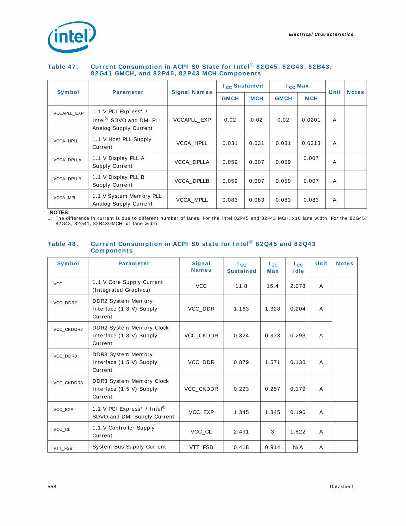
Electrical Characteristics
558 Datasheet
IVCCAPLL_EXP 1.1 V PCI Express* /
Intel® SDVO and DMI PLL Analog Supply Current
VCCAPLL_EXP 0.02 0.02 0.02 0.0201 A
IVCCA_HPLL 1.1 V Host PLL Supply Current
VCCA_HPLL 0.031 0.031 0.031 0.0313 A
IVCCA_DPLLA 1.1 V Display PLL A Supply Current
VCCA_DPLLA 0.059 0.007 0.0590.007
A
IVCCA_DPLLB 1.1 V Display PLL B Supply Current
VCCA_DPLLB 0.059 0.007 0.059 0.007 A
IVCCA_MPLL 1.1 V System Memory PLL Analog Supply Current
VCCA_MPLL 0.083 0.083 0.083 0.083 A
NOTES:1. The difference in current is due to different number of lanes. For the Intel 82P45 and 82P43 MCH, x16 lane width. For the 82G45,
82G43, 82G41, 82B43GMCH, x1 lane width.
Table 48. Current Consumption in ACPI S0 state for Intel® 82Q45 and 82Q43 Components
Symbol Parameter Signal Names
ICC Sustained
ICC Max
ICC Idle
Unit Notes
IVCC 1.1 V Core Supply Current (Integrated Graphics)
VCC 11.8 15.4 2.078 A
IVCC_DDR2 DDR2 System Memory Interface (1.8 V) Supply Current
VCC_DDR 1.163 1.328 0.204 A
IVCC_CKDDR2 DDR2 System Memory Clock Interface (1.8 V) Supply Current
VCC_CKDDR 0.324 0.373 0.293 A
IVCC_DDR3 DDR3 System Memory Interface (1.5 V) Supply Current
VCC_DDR 0.879 1.571 0.130 A
IVCC_CKDDR3 DDR3 System Memory Clock Interface (1.5 V) Supply Current
VCC_CKDDR 0.223 0.257 0.179 A
IVCC_EXP 1.1 V PCI Express* / Intel® SDVO and DMI Supply Current
VCC_EXP 1.345 1.345 0.196 A
IVCC_CL 1.1 V Controller Supply Current
VCC_CL 2.491 3 1.822 A
IVTT_FSB System Bus Supply Current VTT_FSB 0.418 0.914 N/A A
Table 47. Current Consumption in ACPI S0 State for Intel® 82G45, 82G43, 82B43, 82G41 GMCH, and 82P45, 82P43 MCH Components
Symbol Parameter Signal NamesICC Sustained ICC Max
Unit NotesGMCH MCH GMCH MCH

Datasheet 559
Electrical Characteristics
Table 49 shows the maximum power consumption for the Intel 82Q45 GMCH in the ACPI S3, S4, and S5 states with Intel Active Management Technology support. Platforms that use Intel Active Management Technology will keep DRAM memory powered in S4 and S5. Current consumption used by the (G)MCH will vary between the "Idle" case and the "Max" case, depending on activity on the Intel Management Engine. For the majority of the time, the Intel Management Engine will be in the "Idle" state. It is unknown if commercial software management applications will be able to generate this level of power consumption
IVCCA_EXP 1.5 V PCI Express* / Intel® SDVO and DMI Analog Supply Current
VCCA_EXP 0.006 0.006 N/A A
IVCCA_DAC 3.3 V Display DAC Analog Supply Current
VCCA_DAC 0.074 0.074 N/A A
IVCC3_3 3.3 V CMOS Supply Current VCC3_3 0.014 0.014 N/A A
IVCCDQ_CRT 1.5 V Display Quiet Digital Supply Current
VCCDQ_CRT 0 0 N/A A
IVCCAPLL_EXP 1.1 V PCI Express* / Intel® SDVO and DMI PLL Analog Supply Current
VCCAPLL_EXP
0.02 0.02 N/A A
IVCCA_HPLL 1.1 V Host PLL Supply Current VCCA_HPLL 0.031 0.031 N/A A
IVCCA_DPLLA 1.1 V Display PLL A Supply Current
VCCA_DPLLA
0.059 0.059 N/A A
IVCCA_DPLLB 1.1 V Display PLL B Supply Current
VCCA_DPLLB
0.059 0.059 N/A A
IVCCA_MPLL 1.1 V System Memory PLL Analog Supply Current
VCCA_MPLL 0.083 0.083 N/A A
Table 48. Current Consumption in ACPI S0 state for Intel® 82Q45 and 82Q43 Components
Symbol Parameter Signal Names
ICC Sustained
ICC Max
ICC Idle
Unit Notes
Table 49. Current Consumption in S3, S4, S5 with Intel® Active Management Technology Operation (Intel® 82Q45 GMCH Only)
Symbol Parameter Signal Names Idle Max Unit Notes
IMCH_CL1.1 V Supply Current for (G)MCH with Intel AMT
VCC_CL 2.014 2.389 A
IDDR2_PLATFORM
DDR2 System Memory Interface (1.8 V) Supply Current in Standby States with Intel AMT
VCC_DDR, VCC_CKDDR
0.17 0.19 A
IDDR3_PLATFORM
DDR3 System Memory Interface (1.5 V) Supply Current in Standby States with Intel AMT
VCC_DDR, VCC_CKDDR
0.054 0.092 A

Electrical Characteristics
560 Datasheet
14.3 (G)MCH Buffer Supply and DC Characteristics
14.3.1 I/O Buffer Supply Voltages
The I/O buffer supply voltage is measured at the (G)MCH package pins. The tolerances shown in Table 50 are inclusive of all noise from DC up to 20 MHz. In the lab, the voltage rails should be measured with a bandwidth limited oscilloscope with a roll off of 3 dB/decade above 20 MHz under all operating conditions.
Table 50 indicates which supplies are connected directly to a voltage regulator or to a filtered voltage rail. For voltages that are connected to a filter, they should me measured at the input of the filter.
If the recommended platform decoupling guidelines cannot be met, the system designer will have to make tradeoffs between the voltage regulator output DC tolerance and the decoupling performance of the capacitor network to stay within the voltage tolerances listed in Table 50.
Table 50. I/O Buffer Supply Voltage
Symbol Parameter Min Nom Max Unit Notes
VCC_DDRDDR2 I/O Supply Voltage 1.71 1.8 1.89 V
DDR3 I/O Supply Voltage 1.425 1.5 1.575 V
VCC_CKDDRDDR2 Clock Supply Voltage 1.71 1.8 1.89 V 3
DDR3 Clock Supply Voltage 1.425 1.5 1.575 V
VCC_EXP (Intel 82P45,
82P43, 82Q45, 82Q43, 82B43, 82G41 GMCH)
SDVO, PCI Express* Supply Voltage 1.045 1.1 1.155 V
VCC_EXP (Intel 82G45, 82G43 GMCH)
SDVO, PCI Express* Supply Voltage 1.095 1.125 1.155 V
VCCA_EXP SDVO, PCI Express* Analog Supply Voltage 1.425 1.5 1.575 V 3
VTT_FSB 1.2 V System Bus Input Supply Voltage 1.14 1.2 1.26 V
VCC (Intel 82P45, 82P43 MCH,
82Q45, 82Q43, 82B43, 82G41
GMCH)
(G)MCH Core Supply Voltage 1.045 1.1 1.155 V
VCC (Intel 82G45, 82G43 GMCH)
GMCH Core Supply Voltage 1.095 1.125 1.155 V
VCC_CL Controller Supply Voltage 1.045 1.1 1.155 V
VCC3_3 CMOS Supply Voltage 3.135 3.3 3.465 V

Datasheet 561
Electrical Characteristics
VCCA_DAC Display DAC Analog Supply Voltage 3.135 3.3 3.465 V 1
VCCDQ_CRT Display Quiet Digital Supply Voltage 1.425 1.5 1.575 V 2
VCCAPLL_EXP, VCCDPPL_EXP, VCCA_DPLLA, VCCA_DPLLB, VCCA_HPLL, VCCD_HPLL, VCCA_MPLL
Various PLL’s Analog Supply Voltages 1.045 1.1 1.155 V 3, 4
NOTES:1. VCCA_DAC voltage tolerance should only be measured when the DAC is turned ON and at a stable resolution setting. Any noise
on the DAC during power on or display resolution changes do not impact the circuit.2. The VCCDQ_CRT can also operate at a nominal 1.8 V ±5% input voltage. Only the 1.5 V nominal voltage setting will be validated
internally.3. These rails are filtered from other voltage rails on the platform and should be measured at the input of the filter. 4. The noise specifications for VCCA_DPLLA, VCCA_DPPLB, VCCA_HPLL, VCCD_HPLL and VCCA_MPLL are 50, 50, 70, 70 and 70
respectively in mVpp.
Table 50. I/O Buffer Supply Voltage
Symbol Parameter Min Nom Max Unit Notes

Electrical Characteristics
562 Datasheet
14.3.2 General DC Characteristics
Platform Reference Voltages at the top of Table 51 are specified at DC only. VREF measurements should be made with respect to the supply voltage.
Table 51. DC Characteristics
Symbol Parameter Min Nom Max Unit Notes
Reference Voltages
FSB_DVREF FSB_ACCVREF
Host Data, Address, and Common Clock Signal Reference Voltages
0.635 x VTT_FSB – 2%
0.635 x VTT_FSB
0.635 x VTT_FSB + 2%
V
FSB_SWINGHost Compensation Reference Voltage
0.25 x VTT_FSB – 2%
0.25 x VTT_FSB
0.25 x VTT_FSB + 2%
V
CL_VREFController Link Reference Voltage
0.3325 0.35 0.3675 V
DDR_VREF DDR2 Reference Voltage 0.85 0.9 0.95 V
DDR_VREF DDR3 Reference Voltage 0.70 0.75 0.80 V
Host Interface
VIL_H Host GTL+ Input Low Voltage -0.072 0(0.635 x
VTT_FSB) – 0.072
V
VIH_H Host GTL+ Input High Voltage(0.635 x
VTT_FSB) + 0.072
VTT_FSBVTT_FSB +
0.072V
VOL_HHost GTL+ Output Low Voltage
— —(0.25 x
VTT_FSB) + 0.072
V
VOH_HHost GTL+ Output High Voltage
VTT_FSB – 0.072
— VTT_FSB V
IOL_HHost GTL+ Output Low Current
— —VTT_FSBmax *
(1 – 0.25) / Rttmin
mARttmin
= 47.5 Ω
ILEAK_HHost GTL+ Input Leakage Current
— — TBD μA
VOL<Vpad<VTT_F
SB
CPAD Host GTL+ Input Capacitance 1.5 — 2.5 pF
CPCKGHost GTL+ Input Capacitance (common clock)
TBD — TBD pF
DDR2 System Memory Interface
VIL(DC) DDR2 Input Low VoltageDDR_VREF –
100 mVDDR_VREF –
100 mVDDR_VREF –
100 mVV
VIH(DC) DDR2 Input High VoltageDDR_VREF +
100 mVDDR_VREF +
100 mVDDR_VREF +
100 mVV
VIL(AC) DDR2 Input Low VoltageDDR_VREF –
125 mVDDR_VREF –
125 mVDDR_VREF –
125 mVV
VIH(AC) DDR2 Input High VoltageDDR_VREF +
125 mVDDR_VREF +
125 mVDDR_VREF +
125 mVV
VOL DDR2 Output Low Voltage 0.6 0.64 0.67 V 1

Datasheet 563
Electrical Characteristics
VOH DDR2 Output High Voltage 1.45 1.54 1.62 V 1
ILeak Input Leakage Current <0.1 <0.1 <0.1 µA 2
ILeak Input Leakage Current <0.1 <0.1 <0.1 µA 3
CI/ODQ/DQS/DQSB DDR2 Input/Output Pin Capacitance
2.3 2.3 2.3 pF
DDR3 System Memory Interface
VIL(DC) DDR3 Input Low VoltageDDR_VREF –
100 mVDDR_VREF –
100 mVDDR_VREF –
100 mVV
VIH(DC) DDR3 Input High VoltageDDR_VREF +
100 mVDDR_VREF +
100 mVDDR_VREF +
100 mVV
VIL(AC) DDR3 Input Low VoltageDDR_VREF –
125 mVDDR_VREF –
125 mVDDR_VREF –
125 mVV
VIH(AC) DDR3 Input High VoltageDDR_VREF +
125 mVDDR_VREF +
125 mVDDR_VREF +
125 mVV
VOL DDR3 Output Low Voltage 0.6 0.64 0.67 V 1
VOH DDR3 Output High Voltage 1.45 1.52 1.62 V 1
ILeak Input Leakage Current <0.1 <0.1 <0.1 µA 2
ILeak Input Leakage Current <0.1 <0.1 <0.1 µA 3
CI/ODQ/DQS/DQSB DDR3 Input/Output Pin Capacitance
2.3 2.3 2.3 pF
1.1 V PCI Express* Interface 2.0 (includes PCI Express* / Intel® sDVO / DVI / HDMI /DP)
VTX-DIFF P-PDifferential Peak to Peak Output Voltage
0.8 1.0 1.2 V 4
VTX_CM-ACpAC Peak Common Mode Output Voltage
— — 60 mV
ZTX-DIFF-DC DC Differential TX Impedance 80 100 120 ?
VRX-DIFF p-pDifferential Peak to Peak Input Voltage
0.175 — 1.2 V 5
VRX_CM-ACpAC Peak Common Mode Input Voltage
— —[email protected] GHz
300@100 MHzmV
HPD (Hot Plug Detect)
VIL Input Low Voltage — — 200 mV
VIH Input High Voltage 600 — mV
Input Clocks
VIL Input Low Voltage -0.30 0 — V
VIH Input High Voltage — — 1.15 V
VCROSS(ABS) Absolute Crossing Voltage 0.300 — 0.550 V 6, 7, 8
ΔVCROSS(REL) Range of Crossing Points — — 0.140 V
CIN Input Capacitance 1.0 — 3.0 pF
SDVO_CTRLDATA, SDVO_CTRLCLK, DDPC_CTRLDATA, DDPC_CTRCLK
VIL Input Low Voltage — — 0.75 V
VIH Input High Voltage 1.75 — — V
Table 51. DC Characteristics
Symbol Parameter Min Nom Max Unit Notes

Electrical Characteristics
564 Datasheet
ILEAK Input Leakage Current — — ± 10 μA
CIN Input Capacitance — — 10.0 pF
IOLOutput Low Current (CMOS Outputs)
— — 7.8 mA@
50% swing
IOHOutput High Current (CMOS Outputs)
-1 — — mA@
50% swing
VOLOutput Low Voltage (CMOS Outputs)
— — 0.4 V
VOHOutput High Voltage (CMOS Outputs)
2.25 — — V
CRT_DDC_DATA, CRT_DDC_CLK
VIL Input Low Voltage — — 0.3 * VCCP V
VIH Input High Voltage 0.6 * VCCP — — V
ILEAK Input Leakage Current — — TBD μA
CIN Input Capacitance — — 10.0 pF
IOLOutput Low Current (CMOS Outputs)
— — — mA@
50% swing
IOHOutput High Current (CMOS Outputs)
— — — mA@
50% swing
VOLOutput Low Voltage (CMOS Outputs)
— — 0.4@3mA V
VOHOutput High Voltage (CMOS Outputs)
— — — V
HDA_BCLK, HDA_SDI
VIL Input Low Voltage — — 0.4 * VCCP V
VIH Input High Voltage 0.6 * VCCP — — V
ILEAK Input Leakage Current — — ±10 μA
CIN Input Capacitance — — 7.5 pF
VOLOutput Low Voltage (CMOS Outputs)
— — 0.10 * Vcc V
VOHOutput High Voltage (CMOS Outputs)
0.9 * Vcc — — V
CL_DATA, CL_CLK
VIL Input Low Voltage — Vref – 80mV — V
VIH Input High Voltage — Vref + 80mV — V
ILEAK Input Leakage Current — — μA
CIN Input Capacitance — 5 — pF
IOLOutput Low Current (CMOS Outputs)
— ~1 — mA@VOL_
HI max
Table 51. DC Characteristics
Symbol Parameter Min Nom Max Unit Notes

Datasheet 565
Electrical Characteristics
IOHOutput High Current (CMOS Outputs)
6.2 8 9.8 mA@VOH_
HI min
VOLOutput Low Voltage (CMOS Outputs)
— 0 — V
VOHOutput High Voltage (CMOS Outputs)
0.62 0.8 0.98 V
PWROK, CL_PWROK, RSTIN#
VIL Input Low Voltage 1.05 1.081 1.122 V
VIH Input High Voltage 1.93 2.011 2.093 V
ILEAK Input Leakage Current 50 75 120 μA
CIN Input Capacitance 477.292 503.396 531.486 fF
CL_RST#
VIL Input Low Voltage VSS — Vref – 80 mV V
VIH Input High Voltage Vref + 80mV — VCC V
ILEAK Input Leakage Current — — ±20 μA
CIN Input Capacitance — — 2.0 pF
ICH_SYNCB
IOLOutput Low Current (CMOS Outputs)
— — 2.0 mA@VOL_
HI max
IOHOutput High Current (CMOS Outputs)
-2.0 — — mA@VOH_
HI min
VOLOutput Low Voltage (CMOS Outputs)
— — 0.33 V
VOHOutput High Voltage (CMOS Outputs)
2.97 — — V
CRT_HSYNC, CRT_VSYNC
IOLOutput Low Current (CMOS Outputs)
— — — mA@VOL_
HI max
IOHOutput High Current (CMOS Outputs)
— — — mA@VOH_
HI min
VOLOutput Low Voltage (CMOS Outputs)
0 — 0.5@ 8mA V
VOHOutput High Voltage (CMOS Outputs)
2.4 – 8mA — 3.6 V
NOTES:1. Determined with 2x (G)MCH Buffer Strength Settings into a 50 to 0.5xVCC_DDR test load. 2. Applies to pin to VCC or VSS leakage current for the DDR_A_DQ_63:0 and DDR_B_DQ_63:0 signals.3. Applies to pin to pin leakage current between DDR_A_DQS_7:0, DDR_A_DQSB_7:0, DDR_B_DQS_7:0, and DDR_B_DQSB_7:0
signals.4. Specified at the measurement point into a timing and voltage compliance test load as shown in Transmitter compliance eye diagram
of PCI Express* specification and measured over any 250 consecutive TX Uls. 5. Specified at the measurement point over any 250 consecutive Uls. The test load shown in Receiver compliance eye diagram of PCI
Express* spec should be used as the RX device when taking measurements.6. Crossing voltage defined as instantaneous voltage when rising edge of BCLK0 equals falling edge of BCLK1.7. VHavg is the statistical average of the VH measured by the oscilloscope.8. The crossing point must meet the absolute and relative crossing point specifications simultaneously. Refer to the appropriate
processor datasheet for further information.
Table 51. DC Characteristics
Symbol Parameter Min Nom Max Unit Notes

Electrical Characteristics
566 Datasheet
14.3.3 R, G, B / CRT DAC Display DC Characteristics (Intel® 82Q45, 82Q43, 82B43, 82G45, 82G43, 82G41 GMCH Only)
14.3.4 Di/dt Characteristics
To decrease voltage regulator costs, design time and to improve voltage regulator efficiency, di/dt values can be used for these purposes. Also, di/dt values can be used to understand how customer's Voltage Regulator (VR) feedback mechanism has to work to limit the noise within voltage tolerance specifications.
For example, when a sudden current change (di/dt) is seen by VR, it will not follow that demand, it will have some slow response. During that time, its output voltage will tend to go low, if the response is not fast enough, they will violate voltage tolerance specifications.
Cost of VR is also a function of how fast the response time is, by having di/dt data, customers can hold dV in voltage tolerance specifications using minimum cost.
Two sets of di/dt values are provided:
"at VR level: used to optimize VR
"at package pin level: used to optimize motherboard edge capacitor
Table 52. R, G, B / CRT DAC Display DC Characteristics: Functional Operating Range(VCCA_DAC = 3.3 V 5%)
Parameter Min Typical Max Unit Notes
DAC Resolution — 8 — Bits 1
NOTES:1. Measured at each R, G, B termination according to the VESA Test Procedure - Evaluation of Analog Display Graphics Subsystems
Proposal (Version 1, Draft 4, December 1, 2000).
Max Luminance (full-scale) .665 .700 .770 V 1, 2, 4 (white video level voltage)
2. Max steady-state amplitude
Min Luminance — 0.000 — V 1, 3, 4 (black video level voltage)
3. Min steady-state amplitude4. Defined for a double 75 ohm termination.
LSB Current 73.2 — uA 4,5
5. Set by external reference resistor value.
Integral Linearity (INL) -1.0 — +1.0 LSB 1,6
6. INL and DNL measured and calculated according to VESA Video Signal Standards.
Differential Linearity (DNL) -1.0 — +1.0 LSB 1,6
Video channel-channel voltage amplitude mismatch
— — 6 % 7
7. Max full-scale voltage difference among R, G, B outputs (percentage of steady-state full-scale voltage).
Monotonicity Ensured

Datasheet 567
Electrical Characteristics
Table 53 shows the simulated di/dt data at different level for main power rails.
§ §
Table 53. Di/dt Simulation Data
Rail di/dt @ VR di/dt @ package pin
VTT ~ 2mA/ns ~ 750 mA/ns
VCC_DDR ~ 4mA/ns ~ 1.5 A/ns
VCC ~ 2.8A/us~ 6 A/us (VR design)
~ 4 A/100ns (edge cap)
VCC_CL ~ 2.8A/us ~ 2 mA/us
VCC_PEG ~ 3.5mA/ns ~ 15 mA/ns
VCC_DMI ~ 1mA/ns ~ 3.5 mA/ns

Electrical Characteristics
568 Datasheet

Datasheet 569
Ballout and Package Specifications
15 Ballout and Package Specifications
This chapter details the (G)MCH ballout and package specifications.
15.1 Ballout
Figure 18, Figure 19, and Figure 20 show the (G)MCH ballout from a top of the package view. Table 54 lists the ballout arranged alphabetically by signal name.
Note: Notes for Figure 18, Figure 19, Figure 20, and Table 54.
1. Balls that are listed as RSVD are reserved.
2. Balls that are listed as NC are No Connects.
3. Analog Display Signals (CRT_RED, CRT_REDB, CRT_GREEN, CRT_GREENB, CRT_BLUE, CRT_BLUEB, CRT_IREF, CRT_HSYNC, CRT_VSYNC, CRT_DDC_CLK, CRT_DDC_DATA) and the SDVO_CTRLCLK and SDVO_CTRLDATA signals are not used on the 82P45 and 82P42 MCH. Contact your Intel field representative for proper termination of the corresponding balls.
4. For the 82Q45, 82Q43, 82B43, 82G45, 82G43, 82G41 GMCH, the PCI Express and SDVO/HDMI signals are multiplexed. However, only the PCI Express signal name is included in the following ballout figures and table. See Section 2.8 for the signal name mapping.

Ballout and Package Specifications
570 Datasheet
Figure 18. GMCH Ballout Diagram (Top View Left – Columns 45–31)45 44 43 42 41 40 39 38 37 36 35 34 33 32 31
BE RSVD NC VSS VSS DDR_B_MA_13 VCC_SM VSS VCC_SM BE
BD NC VSS VSS DDR_B_ODT_3
DDR_B_CSB_3
DDR_B_CSB_1 VCC_SM DDR_B_O
DT_0DDR_B_W
EBDDR_B_RA
SB VCC_SM DDR_A_MA_4
DDR_A_MA_8 BD
BC VSS DDR_SPU DDR_SPD DDR_A_MA_0
DDR_B_ODT_1
DDR_B_CASB
DDR_A_MA_1
DDR_A_MA_3 BC
BB DDR_VREF DDR3_A_MA0 VCC_SM DDR_B_O
DT_2DDR_B_CS
B_2DDR_B_CS
B_0DDR_A_MA
_2DDR_A_MA
_5 BB
BA DDR_RPU VCC_SM DDR_A_CKB_0
DDR_A_MA_7 BA
AY VSS DDR_A_BS_1 DDR_RPD VCC_SM DDR_A_CK
B_5DDR_A_CK
_0DDR_B_CK
B_2DDR_B_CK
_0DDR_A_MA
_6 AY
AW NC DDR_A_MA_10
DDR_A_WEB
DDR_B_DQ_37
DDR_A_CK_5
DDR_B_CK_5
DDR_B_CK_2
DDR_B_CKB_0
DDR_B_CKB_1 AW
AV DDR_A_BS_0 VCC_SM DDR_A_RA
SBDDR3_B_O
DT3DDR_B_D
Q_36 VSS DDR_A_CKB_2
DDR_B_CKB_5 VSS DDR_B_CK
_1 AV
AU DDR_A_CSB_2
DDR_A_CSB_0
DDR_A_CASB
DDR_B_DQ_39
DDR_B_DQ_38
DDR_B_DM_4
DDR_B_DQ_33
DDR_A_CK_2 VSS DDR_A_CK
_3DDR_B_CK
B_3 AU
AT VCC_SM DDR3_A_WEB VSS DDR_A_CK
B_3DDR_B_CK
_3 AT
AR DDR_A_ODT_2
DDR3_A_CSB1
DDR_A_ODT_0
DDR_A_CSB_1 VSS DDR_B_D
QS_4DDR_B_D
QSB_4DDR_B_D
Q_32 VSS VSS VSS AR
AP VSS VCC_SM DDR_B_CK_4 AP
AN DDR_B_DQ_45
DDR_B_DQ_44 VSS DDR_B_D
Q_35 VSS DDR_B_DQ_34 VSS AN
AM DDR_A_ODT_1
DDR_A_CSB_3
DDR_A_MA_13
VCC_SMCLK AM
AL VSS VSS DDR_A_DQ_36
DDR_A_DQ_32
DDR_A_ODT_3
DDR_B_DQ_47 VSS DDR_B_D
M_5DDR_B_D
Q_41DDR_B_D
Q_40DDR_B_D
QSB_5VCC_SMCL
KVCC_SMCL
K AL
AK DDR_A_DQ_37
DDR_A_DQ_33
DDR_A_DM_4
DDR_B_DQ_52 VSS VSS DDR_B_D
Q_46DDR_B_D
Q_42 VSS DDR_B_DQS_5 RSVD VCC_SMCL
K VCC_CL AK
AJ VSS VSS DDR_B_DQ_53 VSS DDR_B_D
Q_48DDR_B_D
Q_49 VSS DDR_B_DM_6
DDR_B_DQ_43 RSVD VCC_CL VCC_CL AJ
AH DDR_A_DQ_38
DDR_A_DQS_4
DDR_A_DQSB_4 AH
AG VSS DDR_A_DQ_35
DDR_A_DQ_34
DDR_A_DQ_39 VCC_CL AG
AF DDR_A_DQ_45
DDR_A_DQ_40
DDR_A_DQ_41
DDR_A_DQ_44 VSS DDR_B_D
Q_50DDR_B_D
QS_6DDR_B_D
QSB_6 VSS DDR_B_DQ_54 VSS VCC_CL VCC_CL AF
AE DDR_A_DM_5 VSS DDR_A_DQ
SB_5 VSS DDR_B_DQ_61 VSS DDR_B_D
Q_51DDR_B_D
Q_60DDR_B_D
Q_55 VSS VCC_CL VCC_CL VCC_CL AE
AD DDR_A_DQ_46
DDR_A_DQS_5 NC DDR_B_D
Q_56 VSS DDR_B_DQ_57
DDR_B_DM_7 VSS DDR_B_D
QSB_7 VSS VCC_CL VCC_CL VCC_CL AD
AC VSS DDR_A_DQ_42
DDR_A_DQ_43
DDR_A_DQ_47 VCC_CL AC
AB DDR_A_DQ_53
DDR_A_DQ_48
DDR_A_DQ_52
DDR_B_DQ_58 VSS DDR_B_D
Q_63DDR_B_D
Q_62 VSS DDR_B_DQS_7 VSS VCC_CL VCC_CL VCC_CL AB
AA DDR_A_DM_6 VSS DDR_A_DQ
_49 VSS DDR_B_DQ_59 VSS FSB_AB_3
4FSB_AB_3
5FSB_AB_2
9 VSS VCC_CL VCC_CL VCC_CL AA
Y DDR_A_DQ_54
DDR_A_DQS_6
DDR_A_DQSB_6
DDR_A_DQ_55 VSS FSB_AB_3
3FSB_AB_3
1FSB_AB_2
7 VSS FSB_AB_32 VCC_CL VCC_CL VCC_CL Y
W VSS VSS DDR_A_DQ_50
DDR_A_DQ_51 VCC_CL W
V DDR_A_DQ_60
DDR_A_DQ_61
DDR_A_DQ_56 V
U DDR_A_DQ_57 VSS FSB_AB_2
5 VSS FSB_AB_22
FSB_AB_30 VSS FSB_AB_2
8FSB_AB_2
4VCCD_HPL
L NC RSVD U
T DDR_A_DQS_7
DDR_A_DQSB_7
DDR_A_DM_7 VSS FSB_ADST
BB_1 VSS FSB_AB_23
FSB_AB_17 VSS FSB_AB_2
6 VSS VSS VSS T
R VSS DDR_A_DQ_63 NC DDR_A_DQ
_62DDR_A_DQ
_58FSB_AB_2
1 VSS FSB_AB_20
FSB_AB_18
FSB_AB_16
FSB_AB_19 RSVD RSVD R
P DDR_A_DQ_59 DPRSTPB SLPB VSS P
N FSB_AB_14
FSB_AB_10 VSS FSB_AB_1
2 VSS FSB_AB_11 VSS N
M FSB_AB_15 VSS FSB_DB_2
5 M
L FSB_RSB_1 FSB_AB_9 FSB_BREQ
0BFSB_TRDY
B VSS FSB_AB_8 FSB_AB_4 FSB_AB_3 VSS FSB_DB_22
FSB_DB_24 L
K VSS FSB_HITMB
FSB_REQB_1 VSS FSB_DSTB
PB_1 K
J FSB_BNRB FSB_DRDYB FSB_ADSB FSB_AB_1
3FSB_ADST
BB_0FSB_REQB
_2 FSB_AB_5 VSS FSB_DB_17
FSB_DB_21
FSB_DSTBNB_1 J
H FSB_HITB VSS FSB_DBSYB
FSB_LOCKB FSB_AB_7 VSS FSB_BPRIB FSB_DB_1
8 VSS VSS H
G FSB_DEFERB
FSB_RSB_0
FSB_RSB_2
FSB_REQB_4
FSB_REQB_0
FSB_DB_20 VSS FSB_DB_2
3FSB_DB_2
8 G
F VSS FSB_DB_0 VSS FSB_AB_6 FSB_DB_9 FSB_DB_19
FSB_DB_50
FSB_DINVB_1
FSB_DB_57 F
E FSB_DB_4 VSS FSB_DB_16 VSS E
D FSB_DB_2 FSB_DB_6 VSS FSB_DB_12
FSB_DB_14
FSB_DB_53
FSB_DSTBNB_3
FSB_DB_54 D
C VSS FSB_DB_1 FSB_REQB_3 FSB_DB_3 FSB_DSTB
PB_0FSB_DB_1
3FSB_DB_5
1FSB_DSTB
PB_3 C
B NC VSS FSB_DB_5 FSB_DB_7 FSB_DINVB_0
FSB_DSTBNB_0 FSB_DB_8 FSB_DB_1
1FSB_DB_1
5FSB_DB_5
2 VSS FSB_DB_56
FSB_DB_49 B
A RSVD NC VSS VSS FSB_DB_10 VSS FSB_DB_5
5 VSS A
45 44 43 42 41 40 39 38 37 36 35 34 33 32 31

Datasheet 571
Ballout and Package Specifications
Figure 19. GMCH Ballout Diagram (Top View Left – Columns 30–16)30 29 28 27 26 25 24 23 22 21 20 19 18 17 16
BE VSS VCC_SM VSS VCC_SM VSS VSS DDR_B_CKE_2 BE
BD DDR_A_MA_9 VCC_SM DDR_A_MA
_14DDR_A_CK
E_1DDR_B_BS
_0 VCC_SM DDR_B_MA_0
DDR_B_MA_3
DDR_B_MA_5 VCC_SM DDR_B_MA
_9DDR_B_MA
_11DDR_B_BS
_2 VSS DDR_A_DQ_23 BD
BC DDR_A_MA_11
DDR_A_BS_2
DDR_B_MA_10
DDR3_DRAMRSTB
DDR_B_MA_6
DDR_B_MA_7
DDR_B_CKE_0
DDR_A_DQ_18 BC
BB DDR_A_MA_12 VSS DDR_A_CK
E_0DDR_B_BS
_1 VSS DDR_B_MA_2
DDR_B_MA_1
DDR_B_MA_4 VSS DDR_B_MA
_8DDR_B_MA
_12DDR_B_CK
E_3DDR_A_DQ
_19 BB
BA DDR_A_CKE_2 VSS DDR_B_MA
_14 BA
AY VSS DDR_A_CKB_1
DDR_A_CKE_3 VSS DDR_A_DQ
_27DDR_A_DQ
_25 VSS DDR_B_CKE_1
DDR_B_DQ_16 VSS AY
AW VSS DDR_A_CK_1 VSS DDR_B_D
Q_28 VSS VSS DDR_A_DQ_24 VSS VSS DDR_B_D
Q_21 AW
AV VSS DDR_B_DQ_27
DDR_B_DQ_25
DDR_B_DM_3
DDR_A_DQ_26
DDR_A_DM_3 VSS DDR_B_D
Q_19DDR_B_D
Q_17 VSS AV
AU VSS DDR_B_DQ_26
DDR_B_DQS_3 VSS DDR_A_DQ
_31 VSS DDR_A_DQ_28 VSS DDR_B_D
M_2DDR_B_D
Q_15 AU
AT DDR_A_CK_4 VSS DDR_B_D
QSB_3DDR_B_D
Q_24 VSS DDR_A_DQSB_3
DDR_A_DQ_29
DDR_B_DQ_22 VSS DDR_B_D
Q_11 AT
AR DDR_A_CKB_4
DDR_B_DQ_31 VSS DDR_B_D
Q_29DDR_A_DQ
_30DDR_A_DQ
S_3DDR_B_D
Q_18DDR_B_D
QS_2DDR_B_D
QSB_2 VSS AR
AP DDR_B_CKB_4 VSS DDR_B_D
Q_30 VSS VSS VSS VSS VSS DDR_B_DQ_20
DDR_B_DQ_14 AP
AN RSVD RSVD VSS VSS VSS VSS VSS DDR_B_DQ_23 NC NC AN
AM VCCCML_DDR VCC_CL VCC_CL VCC_CL VCC_CL VCC_CL VCC_CL VCC_CL VCC_CL VCC_CL AM
AL VCC_CL VCC_CL VCC_CL VCC_CL VCC_CL VCC_CL VCC_CL VCC_CL VCC_CL VCC_CL VCC_CL VCC_CL VCC_CL AL
AK VCC_CL VCC_CL VCC_CL VCC_CL VCC_CL VCC_CL VCC_CL VCC_CL VCC_CL VCC_CL VCC_CL VCC_CL VCC_CL AK
AJ VCC_CL VCC_CL VCC_CL VSS VCC VSS VCC VSS VCC VSS VCC VCC VCC AJ
AH AH
AG VCC_CL VCC VSS VCC VSS VCC VSS VCC VSS VCC VSS VCC VCC AG
AF NC VCC VCC VCC VCC VCC VCC VCC VCC VCC VCC VCC VCC AF
AE NC VCC VCC VSS VCC VSS VCC VSS VCC VSS VCC VCC VCC AE
AD NC VCC VSS VCC VSS VCC VSS VCC VSS VCC VSS VCC VCC AD
AC NC VCC VCC VSS VCC VSS VCC VSS VCC VSS VCC VCC VCC AC
AB VCC VCC VSS VCC VSS VCC VSS VCC VSS VCC VSS VSS VSS AB
AA VCC VCC VCC VSS VCC VSS VCC VSS VCC VSS VCC VSS VSS AA
Y VCC_CL VCC_CL VSS VCC VSS VCC VSS VCC VSS VCC VSS VSS VSS Y
W NC VCC VCC VSS VCC VSS VCC VSS VCC VSS VCC VSS VSS W
V V
U RSVD VCC VCC VCC VCC VCC VCC VCC VCC VSS VSS VSS VSS U
T VSS VCC VCC VCC VCC VCC VCC VCC VCC VSS VSS VSS VSS T
R VSS VCC VCC VCC VCC VTT_FSB VTT_FSB VTT_FSB VTT_FSB VTT_FSB VSS VSS VSS R
P HPL_CLKINN
HPL_CLKINP VSS VSS VTT_FSB VTT_FSB VTT_FSB VTT_FSB VSS VSS P
N VSS VSS VSS RSVD FSB_DB_47 VTT_FSB VTT_FSB VTT_FSB XORTEST VSS N
M FSB_DB_26
FSB_DB_30
FSB_DB_39 VSS VSS VTT_FSB VTT_FSB ALLZTEST RSVD RSVD M
L VSS FSB_DB_37 VSS FSB_DB_3
5FSB_DB_4
5 VTT_FSB VTT_FSB VSS ITPM_ENB VSS L
K FSB_DB_29 VSS FSB_DB_3
6FSB_DSTB
NB_2 VSS VTT_FSB VTT_FSB VSS VSS RSVD K
J FSB_DB_27
FSB_DB_32
FSB_DB_38
FSB_DSTBPB_2
FSB_DB_46 VTT_FSB VTT_FSB RSVD CEN RSVD J
H VSS FSB_DB_34
FSB_DB_40 VSS FSB_DB_4
4 VTT_FSB VTT_FSB VSS EXP_SM VSS H
G FSB_DB_31 VSS VSS FSB_DB_4
3 VSS VTT_FSB VTT_FSB BSCANTEST VSS BSEL1 G
F VSS FSB_DB_33
FSB_DINVB_2
FSB_DB_41
FSB_DB_42 VTT_FSB VTT_FSB DualX8_En
able BSEL0 VSS F
E FSB_DB_62 VTT_FSB VCC3_3 E
D FSB_DINVB_3
FSB_DB_58
FSB_CPURSTB VSS VSS VTT_FSB VTT_FSB VTT_FSB VSS VCCA_DPL
LA VCCA_DAC CRT_GREEN VSS D
C FSB_DB_60
FSB_DB_48 VTT_FSB VTT_FSB FSB_DVRE
FVCCA_DPL
LB CRT_BLUE VSS C
B FSB_DB_61 VSS FSB_DB_6
3 VSS VTT_FSB VTT_FSB FSB_SWING
FSB_ACCVREF
VCCA_HPLL VSS VCCDQ_CR
T VCCA_DAC CRT_RED VSS VCCAPLL_EXP B
A FSB_DB_59 VSS VTT_FSB FSB_RCOM
PVCCA_MPL
L VSS VCCA_EXP A
30 29 28 27 26 25 24 23 22 21 20 19 18 17 16

Ballout and Package Specifications
572 Datasheet
Figure 20. GMCH Ballout Diagram (Top View Left – Columns 15–1)15 14 13 12 11 10 9 8 7 6 5 4 3 2 1
BE VSS DDR_A_DQ_21 VSS DDR_A_D
Q_13DDR_A_D
Q_6 VSS NC RSVD BE
BD DDR_A_DQS_2
DDR_A_DM_2 VSS DDR_A_D
Q_10DDR_A_D
Q_14DDR_A_D
M_1 VSS DDR_A_DQ_2
DDR_A_DQ_7
DDR_A_DQSB_0
DDR_A_DQ_1 VSS NC BD
BC DDR_A_DQ_17
DDR_A_DQ_20
DDR_A_DQSB_1
DDR_A_DQ_12
DDR_A_DQS_0
DDR_A_DM_0
DDR_A_DQ_0 VSS BC
BB DDR_A_DQSB_2
DDR_A_DQ_16
DDR_A_DQ_11
DDR_A_DQS_1
DDR_A_DQ_8
DDR_A_DQ_3 VSS DDR_A_D
Q_4 BB
BA DDR_A_DQ_22
DDR_B_DQ_2 VSS DDR_A_D
Q_5 BA
AY VSS DDR_B_DQ_8
DDR_A_DQ_15
DDR_B_DQ_7
DDR_A_DQ_9
DDR_B_DM_0 CL_DATA CL_CLK VSS AY
AW DDR_B_DQ_10
DDR_B_DQ_13 VSS DDR_B_D
QSB_0DDR_B_D
QS_0DDR_B_D
Q_6DDR_B_D
Q_1 VSS CL_RSTB AW
AV VSS VSS VSS VSS VSS DDR_B_DQ_0 VSS HDA_RSTB VSS HDA_SDO AV
AU DDR_B_DQSB_1
DDR_B_DQ_12
DDR_B_DQ_3 VSS DDR_B_D
Q_5DDR_B_D
Q_4 VSS VSS HDA_BCLK HDA_SYNC HDA_SDI AU
AT DDR_B_DQS_1 VSS VSS VSS VSS AT
AR DDR_B_DM_1 VSS VSS VSS VSS VSS JTAG_TDI DDR3_DRA
M_PWROK PWROK VSS VCC_HDA AR
AP DDR_B_DQ_9 VCC_CL VCC_CL AP
AN CL_VREF JTAG_TCK JTAG_TDO JTAG_TMS CL_PWROK VSS RSTINB AN
AM VCC_CL VCC_CL VCC_CL VCC_CL AM
AL VCC_CL VCC_CL VCC_CL VCC_CL VCC_CL VCC_CL VCC_CL VCC_CL VCC_CL VCC_CL VCC_CL VCC_CL VCC_CL AL
AK NC VCC_CL VCC_EXP VCC_EXP VCC_EXP VCC_EXP VCC_EXP VCC_EXP VCC_EXP VCC_EXP VCC_EXP VCC_EXP VCC_EXP AK
AJ VCC_CL VCC_EXP VCC_EXP VCC_EXP VCC_EXP VCC_EXP VCC_EXP VCC_EXP VCC_EXP VCC_EXP VCC_EXP VCC_EXP AJ
AH VSS VSS VSS AH
AG VCC_EXP VSS DMI_TXN_3
VCCAVRM_EXP
EXP_RBIAS AG
AF VCC_EXP VCC_EXP VSS VSS VSS VSS DMI_RXP_3
DMI_RXN_3 VSS VSS DMI_TXP_
3 VCC DMI_TXN_2 AF
AE VCC_EXP VCC_EXP VSS VSS VSS DMI_RXN_1
DMI_RXP_1 VSS DMI_RXN_
2DMI_RXP_
2DMI_TXN_
1DMI_TXP_
2 VSS AE
AD VCC_EXP VCC_EXP RSVD VSS PEG_RXN_15
PEG_RXP_15 VSS DMI_RXN_
0DMI_RXP_
0 VSS DMI_TXP_1 VSS DMI_TXN_
0 AD
AC VCC_EXP VSS VCC DMI_TXP_0
PEG_TXP_15 AC
AB RSVD VCC_EXP RSVD VSS VSS PEG_RXP_13
PEG_RXN_13 VSS VSS VSS VSS PEG_RXP_
14PEG_TXN_
15 AB
AA VCC_EXP VCC_EXP VSS VSS VSS PEG_RXN_10
PEG_RXP_10 VSS PEG_RXP_
12PEG_RXN_
12PEG_TXP_
14PEG_RXN_
14 VSS AA
Y VCC_EXP VCC_EXP VSS VSS VSS VSS VSS EXP_COMPI
EXP_RCOMPO
EXP_ICOMPO
PEG_TXN_14 VSS VSS Y
W VCC_EXP VSS PEG_TXP_13 VSS VSS W
V VCC PEG_TXN_13
PEG_TXN_12 V
U VCC_EXP VCC_EXP VSS VSS VSS PEG_RXP_8
PEG_RXN_8 VSS PEG_RXN_
9PEG_RXP_
9PEG_TXP_
12 VSS U
T RSVD RSVD VSS VSS VSS VSS VSS VSS VSS VSS VSS VSS PEG_TXP_11 T
R RSVD RSVD VSS VSS PEG_RXN_7
PEG_RXP_7 VSS PEG_RXP_
6PEG_RXN_
6 VSS PEG_RXP_11 VSS PEG_TXN_
11 R
P BSEL2 PEG_RXN_11 VCC PEG_TXP_
10 P
N VSS VSS PEG_RXN_4
PEG_RXP_4 VSS PEG_RXP_
5PEG_RXN_
5 N
M CRT_DDC_CLK
PEG_TXN_10 VSS M
L CRT_DDC_DATA RSVD RSVD VSS VSS VSS PEG_RXN_
3PEG_RXP_
3 VSS VCC PEG_TXN_9 L
K ICH_SYNCB VSS VSS PEG_TXN_
8PEG_TXP_
9 K
J RSVD SDVO_CTRLDATA
DDPC_CTRLCLK VSS VSS PEG_RXN_
2PEG_RXP_
2 VSS VSS VSS PEG_TXP_8 J
H VSS VSS VSS VSS VSS VSS PEG_RXP_1 VCC PEG_TXP_
7 VSS H
G RSVD SDVO_CTRLCLK VSS DPL_REFS
SCLKINNDPL_REFSSCLKINP
PEG_RXN_0
PEG_RXN_1 VSS PEG_TXN_
7 G
F EXP_SLR CRT_IRTN DDPC_CTRLDATA VCC VSS PEG_RXP_
0 VSS VSS VSS F
E DPL_REFCLKINP EXP_CLKN VSS VSS E
D DPL_REFCLKINN
CRT_HSYNC VSS EXP_CLKP PEG_TXN_
2 VSS VSS PEG_TXP_6 D
C CRT_VSYNC
PEG_TXP_0
PEG_TXP_2
PEG_TXN_3 VSS VSS PEG_TXN_
6 VSS C
B DAC_IREF NC VCCDPLL_EXP
PEG_TXN_0 VSS PEG_TXN_
1PEG_TXP_
3PEG_TXP_
4PEG_TXN_
4PEG_TXN_
5PEG_TXP_
5 RSVD B
A VSS VSS PEG_TXP_1 VSS VSS VSS A
15 14 13 12 11 10 9 8 7 6 5 4 3 2 1

Ballout and Package Specifications
Datasheet 573
Table 54. GMCH Ballout Arranged by Signal Name
Signal Names Ball # X[mils] Y[mils]
VTT_FSB A25 -66 -642.3
VTT_FSB B25 -66 -609.3
VTT_FSB B26 -99 -625.6
VTT_FSB C24 -33 -592.1
VTT_FSB C26 -99 -592.1
VTT_FSB D22 31 -560.6
VTT_FSB D23 0 -575.3
VTT_FSB D24 -31 -560.6
VTT_FSB E23 0 -547.7
VTT_FSB F21 70.5 -514.5
VTT_FSB F22 19.5 -514.5
VTT_FSB G21 70.5 -486.5
VTT_FSB G22 19.5 -486.5
VTT_FSB H21 70.5 -458.5
VTT_FSB H22 19.5 -458.5
VTT_FSB J21 70.5 -430.5
VTT_FSB J22 19.5 -430.5
VTT_FSB K21 70.5 -402.5
VTT_FSB K22 19.5 -402.5
VTT_FSB L21 70.5 -374.5
VTT_FSB L22 19.5 -374.5
VTT_FSB M21 70.5 -346.5
VTT_FSB M22 19.5 -346.5
VTT_FSB N20 121.5 -318.9
VTT_FSB N21 70.5 -318.9
VTT_FSB N22 19.5 -318.9
VTT_FSB P20 121.5 -290.9
VTT_FSB P21 70.5 -290.9
VTT_FSB P22 19.5 -290.9
VTT_FSB P24 -19.5 -290.9
VTT_FSB R20 109.2 -254.8
VTT_FSB R23 0 -254.8
VTT_FSB R24 -36.4 -254.8
VSS B17 198 -609.3
VSS A3 579.3 -642.3
VSS A43 -579.3 -642.3
VSS A6 527.9 -642.3
VSS B44 -610.8 -610.8
VSS BC1 642.3 579.3
VSS BC45 -642.3 579.3
VSS BD2 610.8 610.8
VSS BD44 -610.8 610.8
VSS BE3 579.3 642.3
VSS BE43 -579.3 642.3
VSS C1 642.3 -579.3
VSS C45 -642.3 -579.3
VSS F1 642.3 -527.9
VSS A12 330 -642.3
VSS A15 264 -642.3
VSS A19 132 -642.3
VSS A27 -132 -642.3
VSS A31 -264 -642.3
VSS A36 -396 -642.3
VSS A40 -527.9 -642.3
VSS AA1 642.3 -66
VSS AA11 374.5 -70.5
VSS AA12 346.5 -70.5
VSS AA13 318.9 -70.5
VSS AA20 109.2 -72.8
VSS AA22 36.4 -72.8
VSS AA24 -36.4 -72.8
VSS AA26 -109.2 -72.8
VSS AA34 -346.5 -70.5
VSS AA38 -458.5 -70.5
VSS AA40 -514.5 -70.5
VSS AA44 -609.3 -66
VSS AA8 458.5 -70.5
VSS AB11 374.5 -19.5
VSS AB12 346.5 -19.5
VSS AB19 145.6 -36.4
VSS AB21 72.8 -36.4
VSS AB23 0 -36.4
VSS AB25 -72.8 -36.4
VSS AB27 -145.6 -36.4
VSS AB34 -346.5 -19.5
VSS AB36 -402.5 -19.5
VSS AB39 -486.5 -19.5
VSS AB4 560.6 -31
VSS AB6 514.5 -19.5
VSS AB7 486.5 -19.5
VSS AB8 458.5 -19.5
VSS AC20 109.2 0
VSS AC22 36.4 0
VSS AC24 -36.4 0
VSS AC26 -109.2 0
VSS AC45 -642.3 0
Table 54. GMCH Ballout Arranged by Signal Name
Signal Names Ball # X[mils] Y[mils]

Ballout and Package Specifications
574 Datasheet
VSS AC5 547.7 0
VSS AD12 346.5 19.5
VSS AD19 145.6 36.4
VSS AD21 72.8 36.4
VSS AD23 0 36.4
VSS AD25 -72.8 36.4
VSS AD27 -145.6 36.4
VSS AD3 592.1 33
VSS AD34 -346.5 19.5
VSS AD36 -402.5 19.5
VSS AD39 -486.5 19.5
VSS AD6 514.5 19.5
VSS AD9 430.5 19.5
VSS AE1 642.3 66
VSS AE11 374.5 70.5
VSS AE20 109.2 72.8
VSS AE22 36.4 72.8
VSS AE24 -36.4 72.8
VSS AE26 -109.2 72.8
VSS AE34 -346.5 70.5
VSS AE38 -458.5 70.5
VSS AE40 -514.5 70.5
VSS AE44 -609.3 66
VSS AE8 458.5 70.5
VSS AF10 402.5 121.5
VSS AF11 374.5 121.5
VSS AF12 346.5 121.5
VSS AF13 318.9 121.5
VSS AF33 -318.9 121.5
VSS AF35 -374.5 121.5
VSS AF39 -486.5 121.5
VSS AF6 514.5 121.5
VSS AF7 486.5 121.5
VSS AG19 145.6 145.6
VSS AG21 72.8 145.6
VSS AG23 0 145.6
VSS AG25 -72.8 145.6
VSS AG27 -145.6 145.6
VSS AG45 -642.3 132
VSS AG5 547.7 132
VSS AH2 625.6 165
VSS AH3 592.1 165
VSS AH4 560.6 165
Table 54. GMCH Ballout Arranged by Signal Name
Signal Names Ball # X[mils] Y[mils]
VSS AJ20 109.2 182
VSS AJ22 36.4 182
VSS AJ24 -36.4 182
VSS AJ26 -109.2 182
VSS AJ36 -402.5 172.5
VSS AJ39 -486.5 172.5
VSS AJ44 -609.3 198
VSS AJ45 -642.3 198
VSS AK35 -374.5 223.5
VSS AK38 -458.5 223.5
VSS AK39 -486.5 223.5
VSS AL38 -458.5 274.5
VSS AL44 -608.8 264
VSS AL45 -642.3 264
VSS AN33 -321.4 321.4
VSS AN36 -402.5 321.5
VSS AN38 -458.5 321.5
VSS AN7 486.5 321.5
VSS AP20 121.5 346.5
VSS AP22 19.5 346.5
VSS AP24 -19.5 346.5
VSS AP29 -172.5 346.5
VSS AP45 -642.3 330
VSS AR10 401.3 369.5
VSS AR11 357.9 357.9
VSS AR16 223.5 374.5
VSS AR26 -121.5 374.5
VSS AR31 -274.5 374.5
VSS AR33 -321.5 371.4
VSS AR35 -357.9 357.9
VSS AR39 -486.5 369.5
VSS AR8 458.5 369.5
VSS AR9 430.5 369.5
VSS AT1 642.3 396
VSS AT11 369.5 401.3
VSS AT13 321.5 402.5
VSS AT17 172.5 402.5
VSS AT2 608.8 396
VSS AT24 -19.5 402.5
VSS AT29 -172.5 402.5
DDR_A_CKB_3 AT33 -321.5 402.5
VSS AT35 -369.5 401.3
VSS AU20 121.5 430.5
Table 54. GMCH Ballout Arranged by Signal Name
Signal Names Ball # X[mils] Y[mils]
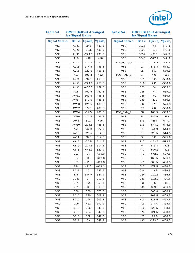
Ballout and Package Specifications
Datasheet 575
VSS AU22 19.5 430.5
VSS AU25 -70.5 430.5
VSS AU30 -223.5 430.5
VSS AU9 418 418
VSS AV13 321.5 458.5
VSS AV15 274.5 458.5
VSS AV16 223.5 458.5
VSS AV2 609.3 462
VSS AV21 70.5 458.5
VSS AV30 -223.5 458.5
VSS AV38 -462.5 462.5
VSS AV8 462.5 462.5
VSS AW11 369.5 486.5
VSS AW17 172.5 486.5
VSS AW20 121.5 486.5
VSS AW22 19.5 486.5
VSS AW24 -19.5 486.5
VSS AW26 -121.5 486.5
VSS AW3 592 495
VSS AW30 -223.5 486.5
VSS AY1 642.3 527.9
VSS AY16 223.5 514.5
VSS AY21 70.5 514.5
VSS AY25 -70.5 514.5
VSS AY30 -223.5 514.5
VSS AY45 -642.3 527.9
VSS B21 66 -609.3
VSS B27 -132 -608.8
VSS B29 -198 -609.3
VSS B34 -330 -609.3
VSS BA23 0 547.7
VSS BA5 544.9 544.9
VSS BB21 64 559.1
VSS BB25 -64 559.1
VSS BB28 -165 560.6
VSS BB6 523 576.3
VSS BD12 330 609.3
VSS BD17 198 609.3
VSS BD8 462 609.3
VSS BE10 396 642.3
VSS BE15 264 642.3
VSS BE19 132 642.3
VSS BE21 66 642.3
Table 54. GMCH Ballout Arranged by Signal Name
Signal Names Ball # X[mils] Y[mils]
VSS BE25 -66 642.3
VSS BE29 -198 642.3
VSS BE34 -330 642.3
VSS BE40 -527.9 642.3
DDR_A_DQ_6 BE6 527.9 642.3
VSS C3 578.3 -578.3
VSS C5 551 -589.9
PEG_TXN_3 C7 495 -592
VSS D11 363 -560.6
VSS D16 231 -560.6
VSS D21 64 -559.1
VSS D25 -64 -559.1
VSS D26 -99 -560.6
VSS D39 -492 -560.6
VSS D6 523 -576.3
VSS D7 492 -560.6
PEG_TXN_2 D8 460.5 -559.1
VSS E3 589.9 -551
VSS E31 -264 -547.7
VSS E41 -544.9 -544.9
VSS E5 544.9 -544.9
VSS F16 223.5 -514.5
VSS F2 609 -525.8
VSS F30 -223.5 -514.5
VSS F4 576.3 -523
VSS F42 -576.3 -523
VSS F45 -642.3 -527.9
VSS F8 465.5 -526.9
VSS G11 369.5 -486.5
VSS G17 172.5 -486.5
VSS G24 -19.5 -486.5
VSS G26 -121.5 -486.5
VSS G29 -172.5 -486.5
VSS G3 592 -495
VSS G35 -369.5 -486.5
VSS H1 642.3 -463.2
VSS H11 369.5 -458.5
VSS H13 321.5 -458.5
VSS H15 274.5 -458.5
VSS H16 223.5 -458.5
VSS H20 121.5 -458.5
VSS H25 -70.5 -458.5
VSS H30 -223.5 -458.5
Table 54. GMCH Ballout Arranged by Signal Name
Signal Names Ball # X[mils] Y[mils]

Ballout and Package Specifications
576 Datasheet
VSS H31 -274.5 -458.5
VSS H33 -321.5 -458.5
VSS H38 -462.5 -462.5
VSS H44 -609.3 -462
VSS H7 497.4 -463
VSS H8 462.5 -462.5
VSS H9 417.5 -458.5
VSS J3 592.1 -429
VSS J37 -418 -418
VSS J4 564.5 -429
VSS J5 539.1 -439.8
VSS J8 458.5 -417.5
VSS J9 418 -418
VSS K13 321.5 -402.5
VSS K17 172.5 -402.5
VSS K20 121.5 -402.5
VSS K24 -19.5 -402.5
VSS K29 -172.5 -402.5
VSS K33 -321.5 -402.5
VSS K45 -642.3 -396
VSS L10 401.3 -369.5
VSS L16 223.5 -374.5
VSS L20 121.5 -374.5
VSS L26 -121.5 -374.5
VSS L30 -223.5 -374.5
VSS L35 -357.9 -357.9
VSS L39 -486.5 -369.5
VSS L4 560.6 -363
VSS L8 458.5 -369.5
VSS L9 430.5 -369.5
VSS M1 642.3 -330
VSS M24 -19.5 -346.5
VSS M25 -70.5 -346.5
VSS M44 -609.3 -330
VSS N11 371.4 -321.5
VSS N13 321.4 -321.4
VSS N26 -121.5 -318.9
VSS N29 -172.5 -318.9
VSS N33 -321.4 -321.4
VSS N36 -402.5 -321.5
VSS N38 -458.5 -321.5
VSS N8 458.5 -321.5
VSS P25 -70.5 -290.9
Table 54. GMCH Ballout Arranged by Signal Name
Signal Names Ball # X[mils] Y[mils]
VSS P26 -121.5 -290.9
VSS R11 374.5 -274.5
VSS R12 346.5 -274.5
VSS R2 608.8 -264
VSS R38 -458.5 -274.5
VSS R45 -642.3 -264
VSS R5 547.7 -264
VSS R8 458.5 -274.5
VSS T10 402.5 -223.5
VSS T11 374.5 -223.5
VSS T12 346.5 -223.5
VSS T13 318.9 -223.5
VSS T3 592.1 -231
VSS T35 -374.5 -223.5
VSS T38 -458.5 -223.5
VSS T4 560.6 -231
VSS T40 -514.5 -223.5
VSS T6 514.5 -223.5
VSS T7 486.5 -223.5
VSS T8 458.5 -223.5
VSS T9 430.5 -223.5
VSS U1 642.3 -198
VSS U11 374.5 -172.5
VSS U12 346.5 -172.5
VSS U13 318.9 -172.5
VSS U36 -402.5 -172.5
VSS U39 -486.5 -172.5
VSS U44 -609.3 -198
VSS U8 458.5 -172.5
VSS W1 642.3 -132
VSS W2 608.8 -132
VSS W20 109.2 -145.6
VSS W22 36.4 -145.6
VSS W24 -36.4 -145.6
VSS W26 -109.2 -145.6
VSS W45 -642.3 -132
VSS W5 547.7 -132
VSS Y10 402.5 -121.5
VSS Y11 374.5 -121.5
VSS Y12 346.5 -121.5
VSS Y13 318.9 -121.5
VSS Y19 145.6 -109.2
VSS Y2 625.6 -99
Table 54. GMCH Ballout Arranged by Signal Name
Signal Names Ball # X[mils] Y[mils]

Ballout and Package Specifications
Datasheet 577
VSS Y21 72.8 -109.2
VSS Y23 0 -109.2
VSS Y25 -72.8 -109.2
VSS Y27 -145.6 -109.2
VSS Y3 592.1 -99
VSS Y35 -374.5 -121.5
VSS Y39 -486.5 -121.5
VSS Y9 430.5 -121.5
VCC_CL AA31 -254.8 -72.8
VCC_CL AB31 -254.8 -36.4
VCC_CL AC31 -254.8 0
VCC_CL AD31 -254.8 36.4
VCC_CL AE31 -254.8 72.8
VCC_CL AF31 -254.8 109.2
VCC_CL AG30 -218.4 145.6
VCC_CL AG31 -254.8 145.6
VCC_CL AJ30 -218.4 182
VCC_CL AJ31 -254.8 182
VCC_CL AK16 218.4 218.4
VCC_CL AK17 182 218.4
VCC_CL AK19 145.6 218.4
VCC_CL AK20 109.2 218.4
VCC_CL AK21 72.8 218.4
VCC_CL AK22 36.4 218.4
VCC_CL AK23 0 218.4
VCC_CL AK24 -36.4 218.4
VCC_CL AK25 -72.8 218.4
VCC_CL AK26 -109.2 218.4
VCC_CL AK27 -145.6 218.4
VCC_CL AK29 -182 218.4
VCC_CL AK30 -218.4 218.4
VCC_CL AL1 642.3 264
VCC_CL AL10 402.5 274.5
VCC_CL AL11 374.5 274.5
VCC_CL AL12 346.5 274.5
VCC_CL AL14 290.5 269.3
VCC_CL AL15 254.8 254.8
VCC_CL AL16 218.4 254.8
VCC_CL AL17 182 254.8
VCC_CL AL19 145.6 254.8
VCC_CL AL2 608.8 264
VCC_CL AL20 109.2 254.8
VCC_CL AL21 72.8 254.8
Table 54. GMCH Ballout Arranged by Signal Name
Signal Names Ball # X[mils] Y[mils]
VCC_CL AL22 36.4 254.8
VCC_CL AL23 0 254.8
VCC_CL AL24 -36.4 254.8
VCC_CL AL25 -72.8 254.8
VCC_CL AL26 -109.2 254.8
VCC_CL AL27 -145.6 254.8
VCC_CL AL29 -182 254.8
VCC_CL AL4 575.3 264
VCC_CL AL5 547.7 264
VCC_CL AL6 514.5 274.5
VCC_CL AL7 486.5 274.5
VCC_CL AL8 458.5 274.5
VCC_CL AL9 430.5 274.5
VCC_CL AM2 625.6 297
VCC_CL AM3 592.1 297
VCC_CL AM4 560.6 297
VCC_CL AP1 642.3 330
VCC_CL AP2 609.3 330
VCC_CL W31 -254.8 -145.6
VCC_CL Y31 -254.8 -109.2
VCC_CL Y29 -182 -109.2
VCC_CL Y30 -218.4 -109.2
VCCDQ_CRT B20 99 -625.6
VCCDPLL_EXP B12 330 -609.3
VCCD_HPLL U33 -318.9 -172.5
VCCCML_DDR AM30 -223.5 290.9
VCC_SMCLK AK32 -290.9 223.5
VCC_SMCLK AL31 -254.8 254.8
VCC_SMCLK AL32 -290.5 269.3
VCC_SMCLK AM31 -269.3 290.5
VCCAVRM_EXP AG2 608.8 132
VCCAPLL_EXP B16 231 -625.6
VCC_CL AJ27 -145.6 182
VCC_CL AJ29 -182 182
VCCA_EXP A17 198 -642.3
VCCA_MPLL A21 66 -642.3
VCCA_HPLL B22 33 -625.6
VCC_CL AA32 -290.9 -70.5
VCC_CL AA33 -318.9 -70.5
VCC_CL AB32 -290.9 -19.5
VCC_CL AB33 -318.9 -19.5
VCC_CL AD32 -290.9 19.5
VCC_CL AD33 -318.9 19.5
Table 54. GMCH Ballout Arranged by Signal Name
Signal Names Ball # X[mils] Y[mils]

Ballout and Package Specifications
578 Datasheet
VCC_CL AE32 -290.9 70.5
VCC_CL AE33 -318.9 70.5
VCC_CL AF32 -290.9 121.5
VCC_CL AJ32 -290.9 172.5
VCC_CL AK31 -254.8 218.4
VCC_CL AL30 -218.4 254.8
VCC_CL AM15 269.3 290.5
VCC_CL AM16 223.5 290.9
VCC_CL AM17 172.5 290.9
VCC_CL AM20 121.5 290.9
VCC_CL AM21 70.5 290.9
VCC_CL AM22 19.5 290.9
VCC_CL AM24 -19.5 290.9
VCC_CL AM25 -70.5 290.9
VCC_CL AM26 -121.5 290.9
VCC_CL AM29 -172.5 290.9
VCC_CL Y32 -290.9 -121.5
VCC_CL Y33 -318.9 -121.5
VCCA_DAC B19 132 -608.8
VCCA_DAC D19 132 -575.3
VCCA_DPLLB C20 99 -592.1
VCCA_DPLLA D20 99 -560.6
VCC_EXP AA14 290.9 -70.5
VCC_EXP AA15 254.8 -72.8
VCC_EXP AB14 290.9 -19.5
VCC_EXP AC15 254.8 0
VCC AC4 575.3 0
VCC_EXP AD14 290.9 19.5
VCC_EXP AD15 254.8 36.4
VCC_EXP AE14 290.9 70.5
VCC_EXP AE15 254.8 72.8
VCC_EXP AF14 290.9 121.5
VCC_EXP AF15 254.8 109.2
VCC AF3 592.1 99
VCC_EXP AG15 254.8 145.6
VCC_EXP AJ10 402.5 172.5
VCC_EXP AJ11 374.5 172.5
VCC_EXP AJ12 346.5 172.5
VCC_EXP AJ13 318.9 172.5
VCC_EXP AJ14 290.9 172.5
VCC_EXP AJ6 514.5 172.5
VCC_EXP AJ7 486.5 172.5
VCC_EXP AJ8 458.5 172.5
Table 54. GMCH Ballout Arranged by Signal Name
Signal Names Ball # X[mils] Y[mils]
VCC_EXP AJ9 430.5 172.5
VCC_EXP AK10 402.5 223.5
VCC_EXP AK11 374.5 223.5
VCC_EXP AK12 346.5 223.5
VCC_EXP AK13 318.9 223.5
VCC_EXP AK6 514.5 223.5
VCC_EXP AK7 486.5 223.5
VCC_EXP AK8 458.5 223.5
VCC_EXP AK9 430.5 223.5
VCC F9 417.5 -520.5
VCC H4 559.1 -460.5
VCC L3 592.1 -363
VCC P3 592.1 -297
VCC_EXP U14 290.9 -172.5
VCC_EXP U15 254.8 -182
VCC V4 560.6 -165
VCC_EXP W15 254.8 -145.6
VCC_EXP Y14 290.9 -121.5
VCC_EXP Y15 254.8 -109.2
VCC_CL AJ15 254.8 182
VCC_CL AK14 290.9 223.5
VCC3_3 E19 132 -547.7
VCC_EXP AJ1 642.3 198
VCC_EXP AJ2 609.3 198
VCC_EXP AK2 625.6 231
VCC_EXP AK3 592.1 231
VCC_EXP AK4 560.6 231
VCC_SM AP44 -609.3 330
VCC_SM AT45 -642.3 396
VCC_SM AV44 -609.3 462
VCC_SM AY40 -525.3 525.3
VCC_SM BA41 -544.9 544.9
VCC_SM BB39 -492 560.6
VCC_SM BD21 66 609.3
VCC_SM BD25 -66 609.3
VCC_SM BD29 -198 609.3
VCC_SM BD34 -330 609.3
VCC_SM BD38 -462 609.3
VCC_SM BE23 0 642.3
VCC_SM BE27 -132 642.3
VCC_SM BE31 -264 642.3
VCC_SM BE36 -396 642.3
VCC_HDA AR2 625.6 363
Table 54. GMCH Ballout Arranged by Signal Name
Signal Names Ball # X[mils] Y[mils]

Ballout and Package Specifications
Datasheet 579
VSS AA16 218.4 -72.8
VSS AA17 182 -72.8
VCC AA19 145.6 -72.8
VCC AA21 72.8 -72.8
VCC AA23 0 -72.8
VCC AA25 -72.8 -72.8
VCC AA27 -145.6 -72.8
VCC AA29 -182 -72.8
VCC AA30 -218.4 -72.8
VSS AB16 218.4 -36.4
VSS AB17 182 -36.4
VCC AB20 109.2 -36.4
VCC AB22 36.4 -36.4
VCC AB24 -36.4 -36.4
VCC AB26 -109.2 -36.4
VCC AB29 -182 -36.4
VCC AB30 -218.4 -36.4
VCC AC16 218.4 0
VCC AC17 182 0
VCC AC19 145.6 0
VCC AC21 72.8 0
VCC AC23 0 0
VCC AC25 -72.8 0
VCC AC27 -145.6 0
VCC AC29 -182 0
VCC AD16 218.4 36.4
VCC AD17 182 36.4
VCC AD20 109.2 36.4
VCC AD22 36.4 36.4
VCC AD24 -36.4 36.4
VCC AD26 -109.2 36.4
VCC AD29 -182 36.4
VCC AE16 218.4 72.8
VCC AE17 182 72.8
VCC AE19 145.6 72.8
VCC AE21 72.8 72.8
VCC AE23 0 72.8
VCC AE25 -72.8 72.8
VCC AE27 -145.6 72.8
VCC AE29 -182 72.8
VCC AF16 218.4 109.2
VCC AF17 182 109.2
VCC AF19 145.6 109.2
Table 54. GMCH Ballout Arranged by Signal Name
Signal Names Ball # X[mils] Y[mils]
VCC AF20 109.2 109.2
VCC AF21 72.8 109.2
VCC AF22 36.4 109.2
VCC AF23 0 109.2
VCC AF24 -36.4 109.2
VCC AF25 -72.8 109.2
VCC AF26 -109.2 109.2
VCC AF27 -145.6 109.2
VCC AF29 -182 109.2
VCC AG16 218.4 145.6
VCC AG17 182 145.6
VCC AG20 109.2 145.6
VCC AG22 36.4 145.6
VCC AG24 -36.4 145.6
VCC AG26 -109.2 145.6
VCC AG29 -182 145.6
VCC AJ16 218.4 182
VCC AJ17 182 182
VCC AJ19 145.6 182
VCC AJ21 72.8 182
VCC AJ23 0 182
VCC AJ25 -72.8 182
VSS N16 223.5 -318.9
VSS P16 223.5 -290.9
VSS P17 172.5 -290.9
VSS R16 218.4 -254.8
VSS R17 182 -254.8
VSS R19 145.6 -254.8
VCC R25 -72.8 -254.8
VCC R26 -109.2 -254.8
VCC R27 -145.6 -254.8
VCC R29 -182 -254.8
VSS R30 -218.4 -254.8
VSS T16 218.4 -218.4
VSS T17 182 -218.4
VSS T19 145.6 -218.4
VSS T20 109.2 -218.4
VCC T21 72.8 -218.4
VCC T24 -36.4 -218.4
VCC T25 -72.8 -218.4
VCC T26 -109.2 -218.4
VCC T27 -145.6 -218.4
VCC T29 -182 -218.4
Table 54. GMCH Ballout Arranged by Signal Name
Signal Names Ball # X[mils] Y[mils]

Ballout and Package Specifications
580 Datasheet
VSS T30 -218.4 -218.4
VSS U16 218.4 -182
VSS U17 182 -182
VSS U19 145.6 -182
VSS U20 109.2 -182
VCC U21 72.8 -182
VCC U22 36.4 -182
VCC U23 0 -182
VCC U24 -36.4 -182
VCC U25 -72.8 -182
VCC U26 -109.2 -182
VCC U27 -145.6 -182
VCC U29 -182 -182
VSS W16 218.4 -145.6
VSS W17 182 -145.6
VCC W19 145.6 -145.6
VCC W21 72.8 -145.6
VCC W23 0 -145.6
VCC W25 -72.8 -145.6
VCC W27 -145.6 -145.6
VCC W29 -182 -145.6
NC W30 -218.4 -145.6
VSS Y16 218.4 -109.2
VSS Y17 182 -109.2
VCC Y20 109.2 -109.2
VCC Y22 36.4 -109.2
VCC Y24 -36.4 -109.2
VCC Y26 -109.2 -109.2
NC B14 297 -625.6
NC AK15 254.8 218.4
NC AE30 -218.4 72.8
NC AF30 -218.4 109.2
NC AC30 -218.4 0
NC AD30 -218.4 36.4
SDVO_CTRLDATA J13 321.5 -430.5
SDVO_CTRLCLK G13 321.5 -486.5
RSVD A45 -642.3 -642.3
RSVD B2 610.8 -610.8
RSVD BE1 642.3 642.3
RSVD BE45 -642.3 642.3
RSTINB AN6 520.5 321.5
PWROK AR4 560.6 363
SLPB P42 -560.6 -297
Table 54. GMCH Ballout Arranged by Signal Name
Signal Names Ball # X[mils] Y[mils]
RSVD L13 321.5 -371.4
DPRSTPB P43 -592.1 -297
RSVD L11 357.9 -357.9
PEG_TXP_9 K1 642.3 -396
PEG_TXP_8 J2 625.6 -429
PEG_TXP_7 H2 609.3 -462
PEG_TXP_6 D2 624 -553.6
PEG_TXP_5 B3 579.6 -605.9
PEG_TXP_4 B7 497.9 -623.9
VSS A8 463.2 -642.3
PEG_TXN_1 B9 429 -625.6
PEG_TXP_15 AC1 642.3 0
PEG_TXP_14 AA4 559.1 -64
PEG_TXP_13 W4 575.3 -132
PEG_TXP_12 U2 609.3 -198
PEG_TXP_11 T2 625.6 -231
PEG_TXP_10 P2 625.6 -297
PEG_TXP_1 A10 396 -642.3
PEG_TXP_0 C11 363 -592.1
PEG_TXN_9 L2 625.6 -363
PEG_TXN_8 K2 608.8 -396
PEG_TXN_7 G2 623.9 -497.9
PEG_TXN_6 C2 605.9 -579.6
PEG_TXN_5 B4 553.6 -624
PEG_TXN_4 B6 525.8 -609
PEG_TXP_3 B8 462 -609.3
PEG_TXP_2 C9 429 -592.1
PEG_TXN_15 AB2 625.6 -33
PEG_TXN_14 Y4 560.6 -99
PEG_TXN_13 V3 592.1 -165
PEG_TXN_12 V2 625.6 -165
PEG_TXN_11 R1 642.3 -264
PEG_TXN_10 M2 609.3 -330
VSS B10 396 -608.8
PEG_TXN_0 B11 363 -625.6
PEG_RXP_9 U6 514.5 -172.5
PEG_RXP_8 U10 402.5 -172.5
PEG_RXP_7 R9 430.5 -274.5
PEG_RXP_6 R7 486.5 -274.5
PEG_RXP_5 N7 486.5 -321.5
PEG_RXP_4 N9 430.5 -321.5
PEG_RXP_3 L6 520.5 -369.5
PEG_RXP_2 J6 520.5 -417.5
Table 54. GMCH Ballout Arranged by Signal Name
Signal Names Ball # X[mils] Y[mils]

Ballout and Package Specifications
Datasheet 581
PEG_RXP_15 AD10 402.5 19.5
PEG_RXP_14 AB3 592.1 -33
PEG_RXP_13 AB10 402.5 -19.5
PEG_RXP_12 AA7 486.5 -70.5
PEG_RXP_11 R4 575.3 -264
PEG_RXP_10 AA9 430.5 -70.5
PEG_RXP_1 H6 526.9 -465.5
PEG_RXP_0 F6 525.3 -525.3
PEG_RXN_9 U7 486.5 -172.5
PEG_RXN_8 U9 430.5 -172.5
PEG_RXN_7 R10 402.5 -274.5
PEG_RXN_6 R6 514.5 -274.5
PEG_RXN_5 N6 520.5 -321.5
PEG_RXN_4 N10 402.5 -321.5
PEG_RXN_3 L7 486.5 -369.5
PEG_RXN_2 J7 486.5 -417.5
PEG_RXN_15 AD11 374.5 19.5
PEG_RXN_14 AA2 609.3 -66
PEG_RXN_13 AB9 430.5 -19.5
PEG_RXN_12 AA6 514.5 -70.5
PEG_RXN_11 P4 560.6 -297
PEG_RXN_10 AA10 402.5 -70.5
PEG_RXN_1 G4 560.6 -492
PEG_RXN_0 G7 505.7 -505.7
ITPM_ENB L17 172.5 -374.5
EXP_SM H17 172.5 -458.5
RSVD G15 274.5 -486.5
EXP_SLR F15 274.5 -514.5
RSVD K16 223.5 -402.5
XORTEST N17 172.5 -318.9
ALLZTEST M20 121.5 -346.5
BSEL2 P15 269.3 -290.5
DualX8_Enable F20 121.5 -514.5
RSVD J20 121.5 -430.5
RSVD J15 274.5 -430.5
RSVD M16 223.5 -346.5
RSVD J16 223.5 -430.5
BSCANTEST G20 121.5 -486.5
CEN J17 172.5 -430.5
RSVD M17 172.5 -346.5
BSEL1 G16 223.5 -486.5
BSEL0 F17 172.5 -514.5
NC A44 -610.8 -642.3
Table 54. GMCH Ballout Arranged by Signal Name
Signal Names Ball # X[mils] Y[mils]
NC BD1 642.3 610.8
NC BD45 -642.3 610.8
NC BE2 610.8 642.3
NC BE44 -610.8 642.3
DDR_A_DQS_5 AD43 -592.1 33
NC AN16 223.5 318.9
VSS AN26 -121.5 318.9
VSS AP21 70.5 346.5
VSS AP25 -70.5 346.5
VSS AR13 321.5 371.4
VSS AR3 592.1 363
VSS AU5 539.1 439.8
VSS AU6 520.5 417.5
VSS AV11 369.5 458.5
DDR_B_CKB_5 AV35 -369.5 458.5
VSS AV6 526.9 465.5
VSS AV9 417.5 458.5
NC AW44 -623.9 497.9
VSS BD43 -579.6 605.9
VSS K11 369.5 -401.3
VSS N30 -223.5 -318.9
VSS P31 -269.3 -290.5
NC R42 -575.3 -264
VSS T31 -254.8 -218.4
VSS T32 -290.9 -223.5
VSS T33 -318.9 -223.5
NC U32 -290.9 -172.5
VSS W44 -608.8 -132
CL_VREF AN13 321.4 321.4
CL_RSTB AW2 623.9 497.9
CL_DATA AY4 576.3 523
CL_CLK AY2 609 525.8
CL_PWROK AN8 458.5 321.5
NC B45 -642.3 -610.8
ICH_SYNCB K15 274.5 -402.5
VTT_FSB R22 36.4 -254.8
VTT_FSB R21 72.8 -254.8
VSS AN22 19.5 318.9
VSS AN21 70.5 318.9
VCC T23 0 -218.4
VCC T22 36.4 -218.4
VSS AE13 318.9 70.5
VSS AE12 346.5 70.5
Table 54. GMCH Ballout Arranged by Signal Name
Signal Names Ball # X[mils] Y[mils]

Ballout and Package Specifications
Datasheet 582
VSS AN24 -19.5 318.9
VSS AN25 -70.5 318.9
JTAG_TMS AN9 430.5 321.5
JTAG_TDO AN10 402.5 321.5
JTAG_TDI AR7 486.5 369.5
JTAG_TCK AN11 371.4 321.5
RSVD U30 -218.4 -182
RSVD U31 -254.8 -182
RSVD R31 -254.8 -254.8
RSVD R32 -290.5 -269.3
HPL_CLKINP P29 -172.5 -290.9
HPL_CLKINN P30 -223.5 -290.9
FSB_TRDYB L40 -520.5 -369.5
FSB_SWING B24 -33 -625.6
FSB_RSB_2 G42 -560.6 -492
FSB_RSB_1 L44 -625.6 -363
FSB_RSB_0 G43 -592 -495
FSB_REQB_4 G39 -505.7 -505.7
FSB_REQB_3 C43 -578.3 -578.3
FSB_REQB_2 J39 -486.5 -417.5
FSB_REQB_1 K35 -369.5 -401.3
FSB_REQB_0 G38 -463 -497.4
FSB_RCOMP A23 0 -642.3
RSVD N25 -70.5 -318.9
FSB_LOCKB H40 -526.9 -465.5
FSB_HITMB K44 -608.8 -396
FSB_HITB H45 -642.3 -463.2
FSB_DVREF C22 33 -592.1
FSB_DSTBPB_3 C32 -297 -592.1
FSB_DSTBPB_2 J25 -70.5 -430.5
FSB_DSTBPB_1 K31 -274.5 -402.5
FSB_DSTBPB_0 C39 -495 -592
FSB_DSTBNB_3 D32 -297 -560.6
FSB_DSTBNB_2 K25 -70.5 -402.5
FSB_DSTBNB_1 J31 -274.5 -430.5
FSB_DSTBNB_0 B39 -497.9 -623.9
FSB_DRDYB J43 -592.1 -429
FSB_DINVB_3 D30 -231 -560.6
FSB_DINVB_2 F26 -121.5 -514.5
FSB_DINVB_1 F33 -321.5 -520.5
FSB_DINVB_0 B40 -525.8 -609
FSB_DEFERB G44 -623.9 -497.9
FSB_DBSYB H42 -559.1 -460.5
Table 54. GMCH Ballout Arranged by Signal Name
Signal Names Ball # X[mils] Y[mils]
FSB_DB_9 F38 -465.5 -526.9
FSB_DB_8 B38 -462 -609.3
FSB_DB_7 B42 -553.6 -624
FSB_DB_63 B28 -165 -625.6
FSB_DB_62 E27 -132 -547.7
FSB_DB_61 B30 -231 -625.6
FSB_DB_60 C30 -231 -592.1
FSB_DB_6 D40 -523 -576.3
FSB_DB_59 A29 -198 -642.3
FSB_DB_58 D28 -165 -560.6
FSB_DB_57 F31 -274.5 -514.5
FSB_DB_56 B32 -297 -625.6
FSB_DB_55 A34 -330 -642.3
FSB_DB_54 D31 -264 -575.3
FSB_DB_53 D35 -363 -560.6
FSB_DB_52 B35 -363 -625.6
FSB_DB_51 C35 -363 -592.1
FSB_DB_50 F35 -369.5 -520.5
FSB_DB_5 B43 -579.6 -605.9
FSB_DB_49 B31 -264 -608.8
FSB_DB_48 C28 -165 -592.1
FSB_DB_47 N24 -19.5 -318.9
FSB_DB_46 J24 -19.5 -430.5
FSB_DB_45 L24 -19.5 -374.5
FSB_DB_44 H24 -19.5 -458.5
FSB_DB_43 G25 -70.5 -486.5
FSB_DB_42 F24 -19.5 -514.5
FSB_DB_41 F25 -70.5 -514.5
FSB_DB_40 H26 -121.5 -458.5
FSB_DB_4 E43 -589.9 -551
FSB_DB_39 M26 -121.5 -346.5
FSB_DB_38 J26 -121.5 -430.5
FSB_DB_37 L29 -172.5 -374.5
FSB_DB_36 K26 -121.5 -402.5
FSB_DB_35 L25 -70.5 -374.5
FSB_DB_34 H29 -172.5 -458.5
FSB_DB_33 F29 -172.5 -514.5
FSB_DB_32 J29 -172.5 -430.5
FSB_DB_31 G30 -223.5 -486.5
FSB_DB_30 M29 -172.5 -346.5
FSB_DB_3 C41 -551 -589.9
FSB_DB_29 K30 -223.5 -402.5
FSB_DB_28 G31 -274.5 -486.5
Table 54. GMCH Ballout Arranged by Signal Name
Signal Names Ball # X[mils] Y[mils]

Ballout and Package Specifications
Datasheet 583
FSB_DB_27 J30 -223.5 -430.5
FSB_DB_26 M30 -223.5 -346.5
FSB_DB_25 M31 -274.5 -346.5
FSB_DB_24 L31 -274.5 -374.5
FSB_DB_23 G33 -321.5 -486.5
FSB_DB_22 L33 -321.5 -371.4
FSB_DB_21 J33 -321.5 -430.5
FSB_DB_20 G37 -417.5 -486.5
FSB_DB_2 D44 -624 -553.6
FSB_DB_19 F37 -417.5 -520.5
FSB_DB_18 H35 -369.5 -458.5
FSB_DB_17 J35 -369.5 -430.5
FSB_DB_16 E37 -439.8 -539.1
FSB_DB_15 B36 -396 -608.8
FSB_DB_14 D37 -429 -564.5
FSB_DB_13 C37 -429 -592.1
FSB_DB_12 D38 -460.5 -559.1
FSB_DB_11 B37 -429 -625.6
FSB_DB_10 A38 -463.2 -642.3
FSB_DB_1 C44 -605.9 -579.6
FSB_DB_0 F44 -609 -525.8
FSB_CPURSTB D27 -132 -575.3
FSB_BREQ0B L42 -560.6 -363
FSB_BPRIB H37 -417.5 -458.5
FSB_BNRB J44 -625.6 -429
FSB_ADSTBB_1 T39 -486.5 -223.5
FSB_ADSTBB_0 J40 -520.5 -417.5
FSB_ADSB J42 -564.5 -429
FSB_ACCVREF B23 0 -608.8
FSB_AB_9 L43 -592.1 -363
FSB_AB_8 L38 -458.5 -369.5
FSB_AB_7 H39 -497.4 -463
FSB_AB_6 F40 -525.3 -525.3
FSB_AB_5 J38 -458.5 -417.5
FSB_AB_4 L37 -430.5 -369.5
FSB_AB_35 AA36 -402.5 -70.5
FSB_AB_34 AA37 -430.5 -70.5
FSB_AB_33 Y38 -458.5 -121.5
FSB_AB_32 Y34 -346.5 -121.5
FSB_AB_31 Y37 -430.5 -121.5
FSB_AB_30 U37 -430.5 -172.5
FSB_AB_3 L36 -401.3 -369.5
FSB_AB_29 AA35 -374.5 -70.5
Table 54. GMCH Ballout Arranged by Signal Name
Signal Names Ball # X[mils] Y[mils]
FSB_AB_28 U35 -374.5 -172.5
FSB_AB_27 Y36 -402.5 -121.5
FSB_AB_26 T34 -346.5 -223.5
FSB_AB_25 U40 -514.5 -172.5
FSB_AB_24 U34 -346.5 -172.5
FSB_AB_23 T37 -430.5 -223.5
FSB_AB_22 U38 -458.5 -172.5
FSB_AB_21 R39 -486.5 -274.5
FSB_AB_20 R37 -430.5 -274.5
FSB_AB_19 R34 -346.5 -274.5
FSB_AB_18 R36 -402.5 -274.5
FSB_AB_17 T36 -402.5 -223.5
FSB_AB_16 R35 -374.5 -274.5
FSB_AB_15 M45 -642.3 -330
FSB_AB_14 N40 -520.5 -321.5
FSB_AB_13 J41 -539.1 -439.8
FSB_AB_12 N37 -430.5 -321.5
FSB_AB_11 N35 -371.4 -321.5
FSB_AB_10 N39 -486.5 -321.5
RSVD AB13 318.9 -19.5
RSVD AD13 318.9 19.5
EXP_RCOMPO Y7 486.5 -121.5
EXP_RBIAS AG1 642.3 132
RSVD AB15 254.8 -36.4
EXP_ICOMPO Y6 514.5 -121.5
EXP_COMPI Y8 458.5 -121.5
EXP_CLKP D9 429 -564.5
EXP_CLKN E9 439.8 -539.1
NC AN17 172.5 318.9
DPL_REFSSCLKINP G8 463 -497.4
DPL_REFSSCLKINN G9 417.5 -486.5
DPL_REFCLKINP E15 264 -547.7
DPL_REFCLKINN D15 264 -575.3
RSVD T14 290.9 -223.5
RSVD T15 254.8 -218.4
RSVD R14 290.5 -269.3
RSVD R15 254.8 -254.8
DMI_TXP_3 AF4 560.6 99
DMI_TXP_2 AE2 609.3 66
DMI_TXP_1 AD4 560.6 31
DMI_TXP_0 AC2 608.8 0
DMI_TXN_3 AG4 575.3 132
DMI_TXN_2 AF2 625.6 99
Table 54. GMCH Ballout Arranged by Signal Name
Signal Names Ball # X[mils] Y[mils]

Ballout and Package Specifications
584 Datasheet
DMI_TXN_1 AE4 559.1 64
DMI_TXN_0 AD2 625.6 33
DMI_RXP_3 AF9 430.5 121.5
DMI_RXP_2 AE6 514.5 70.5
DMI_RXP_1 AE9 430.5 70.5
DMI_RXP_0 AD7 486.5 19.5
DMI_RXN_3 AF8 458.5 121.5
DMI_RXN_2 AE7 486.5 70.5
DMI_RXN_1 AE10 402.5 70.5
DMI_RXN_0 AD8 458.5 19.5
DDR3_DRAMRSTB BC24 -33 592.1
DDR3_DRAM_PWROK
AR6 520.5 369.5
DDR3_B_ODT3 AV40 -526.9 465.5
DDR3_A_WEB AT44 -608.8 396
DDR3_A_MA0 BB40 -523 576.3
DDR3_A_CSB1 AR43 -592.1 363
DDR_VREF BB44 -624 553.6
DDR_SPU BC44 -605.9 579.6
DDR_SPD BC43 -578.3 578.3
DDR_RPU BA43 -589.9 551
DDR_RPD AY42 -576.3 523
RSVD AK33 -318.9 223.5
RSVD AJ33 -318.9 172.5
DDR_B_WEB BD36 -396 608.8
DDR_B_RASB BD35 -363 625.6
DDR_B_ODT_3 BD42 -553.6 624
DDR_B_ODT_2 BB38 -460.5 559.1
DDR_B_ODT_1 BC39 -495 592
DDR_B_ODT_0 BD37 -429 625.6
DDR_B_MA_9 BD20 99 625.6
DDR_B_MA_8 BB20 99 560.6
DDR_B_MA_7 BC20 99 592.1
DDR_B_MA_6 BC22 33 592.1
DDR_B_MA_5 BD22 33 625.6
DDR_B_MA_4 BB22 31 560.6
DDR_B_MA_3 BD23 0 608.8
DDR_B_MA_2 BB24 -31 560.6
DDR_B_MA_14 BA19 132 547.7
DDR_B_MA_13 BE38 -463.2 642.3
DDR_B_MA_12 BB19 132 575.3
DDR_B_MA_11 BD19 132 608.8
DDR_B_MA_10 BC26 -99 592.1
Table 54. GMCH Ballout Arranged by Signal Name
Signal Names Ball # X[mils] Y[mils]
DDR_B_MA_1 BB23 0 575.3
DDR_B_MA_0 BD24 -33 625.6
DDR_B_DQSB_7 AD35 -374.5 19.5
DDR_B_DQSB_6 AF36 -402.5 121.5
DDR_B_DQSB_5 AL34 -346.5 274.5
DDR_B_DQSB_4 AR37 -430.5 369.5
DDR_B_DQSB_3 AT26 -121.5 402.5
DDR_B_DQSB_2 AR17 172.5 374.5
DDR_B_DQSB_1 AU15 274.5 430.5
DDR_B_DQSB_0 AW9 417.5 486.5
DDR_B_DQS_7 AB35 -374.5 -19.5
DDR_B_DQS_6 AF37 -430.5 121.5
DDR_B_DQS_5 AK34 -346.5 223.5
DDR_B_DQS_4 AR38 -458.5 369.5
DDR_B_DQS_3 AU26 -121.5 430.5
DDR_B_DQS_2 AR20 121.5 374.5
DDR_B_DQS_1 AT15 274.5 402.5
DDR_B_DQS_0 AW8 463 497.4
DDR_B_DQ_9 AP15 274.5 346.5
DDR_B_DQ_8 AY13 321.5 520.5
DDR_B_DQ_7 AY9 417.5 520.5
DDR_B_DQ_63 AB38 -458.5 -19.5
DDR_B_DQ_62 AB37 -430.5 -19.5
DDR_B_DQ_61 AE39 -486.5 70.5
DDR_B_DQ_60 AE36 -402.5 70.5
DDR_B_DQ_6 AW7 505.7 505.7
DDR_B_DQ_59 AA39 -486.5 -70.5
DDR_B_DQ_58 AB40 -514.5 -19.5
DDR_B_DQ_57 AD38 -458.5 19.5
DDR_B_DQ_56 AD40 -514.5 19.5
DDR_B_DQ_55 AE35 -374.5 70.5
DDR_B_DQ_54 AF34 -346.5 121.5
DDR_B_DQ_53 AJ40 -514.5 172.5
DDR_B_DQ_52 AK40 -514.5 223.5
DDR_B_DQ_51 AE37 -430.5 70.5
DDR_B_DQ_50 AF38 -458.5 121.5
DDR_B_DQ_5 AU8 458.5 417.5
DDR_B_DQ_49 AJ37 -430.5 172.5
DDR_B_DQ_48 AJ38 -458.5 172.5
DDR_B_DQ_47 AL39 -486.5 274.5
DDR_B_DQ_46 AK37 -430.5 223.5
DDR_B_DQ_45 AN40 -520.5 321.5
DDR_B_DQ_44 AN39 -486.5 321.5
Table 54. GMCH Ballout Arranged by Signal Name
Signal Names Ball # X[mils] Y[mils]

Ballout and Package Specifications
Datasheet 585
DDR_B_DQ_43 AJ34 -346.5 172.5
DDR_B_DQ_42 AK36 -402.5 223.5
DDR_B_DQ_41 AL36 -402.5 274.5
DDR_B_DQ_40 AL35 -374.5 274.5
DDR_B_DQ_4 AU7 486.5 417.5
DDR_B_DQ_39 AU41 -539.1 439.8
DDR_B_DQ_38 AU40 -520.5 417.5
DDR_B_DQ_37 AW39 -505.7 505.7
DDR_B_DQ_36 AV39 -497.4 463
DDR_B_DQ_35 AN37 -430.5 321.5
DDR_B_DQ_34 AN35 -371.4 321.5
DDR_B_DQ_33 AU38 -458.5 417.5
DDR_B_DQ_32 AR36 -401.3 369.5
DDR_B_DQ_31 AR29 -172.5 374.5
DDR_B_DQ_30 AP26 -121.5 346.5
DDR_B_DQ_3 AU11 369.5 430.5
DDR_B_DQ_29 AR25 -70.5 374.5
DDR_B_DQ_28 AW25 -70.5 486.5
DDR_B_DQ_27 AV29 -172.5 458.5
DDR_B_DQ_26 AU29 -172.5 430.5
DDR_B_DQ_25 AV26 -121.5 458.5
DDR_B_DQ_24 AT25 -70.5 402.5
DDR_B_DQ_23 AN20 121.5 318.9
DDR_B_DQ_22 AT20 121.5 402.5
DDR_B_DQ_21 AW16 223.5 486.5
DDR_B_DQ_20 AP17 172.5 346.5
DDR_B_DQ_2 BA9 439.8 539.1
DDR_B_DQ_19 AV20 121.5 458.5
DDR_B_DQ_18 AR21 70.5 374.5
DDR_B_DQ_17 AV17 172.5 458.5
DDR_B_DQ_16 AY17 172.5 514.5
DDR_B_DQ_15 AU16 223.5 430.5
DDR_B_DQ_14 AP16 223.5 346.5
DDR_B_DQ_13 AW13 321.5 486.5
DDR_B_DQ_12 AU13 321.5 430.5
DDR_B_DQ_11 AT16 223.5 402.5
DDR_B_DQ_10 AW15 274.5 486.5
DDR_B_DQ_1 AW4 560.6 492
DDR_B_DQ_0 AV7 497.4 463
DDR_B_DM_7 AD37 -430.5 19.5
DDR_B_DM_6 AJ35 -374.5 172.5
DDR_B_DM_5 AL37 -430.5 274.5
DDR_B_DM_4 AU39 -486.5 417.5
Table 54. GMCH Ballout Arranged by Signal Name
Signal Names Ball # X[mils] Y[mils]
DDR_B_DM_3 AV25 -70.5 458.5
DDR_B_DM_2 AU17 172.5 430.5
DDR_B_DM_1 AR15 274.5 374.5
DDR_B_DM_0 AY6 525.3 525.3
DDR_B_CSB_3 BD40 -525.8 609
DDR_B_CSB_2 BB37 -429 564.5
DDR_B_CSB_1 BD39 -497.9 623.9
DDR_B_CSB_0 BB35 -363 560.6
DDR_B_CKE_3 BB18 165 560.6
DDR_B_CKE_2 BE17 198 642.3
DDR_B_CKE_1 AY20 121.5 514.5
DDR_B_CKE_0 BC18 165 592.1
VSS AU35 -369.5 430.5
DDR_B_CKB_4 AP30 -223.5 346.5
DDR_B_CKB_3 AU31 -274.5 430.5
DDR_B_CKB_2 AY35 -369.5 520.5
DDR_B_CKB_1 AW31 -274.5 486.5
DDR_B_CKB_0 AW33 -321.5 486.5
DDR_B_CK_5 AW37 -417.5 486.5
DDR_B_CK_4 AP31 -274.5 346.5
DDR_B_CK_3 AT31 -274.5 402.5
DDR_B_CK_2 AW35 -369.5 486.5
DDR_B_CK_1 AV31 -274.5 458.5
DDR_B_CK_0 AY33 -321.5 520.5
DDR_B_CASB BC37 -429 592.1
DDR_B_BS_2 BD18 165 625.6
DDR_B_BS_1 BB26 -99 560.6
DDR_B_BS_0 BD26 -99 625.6
RSVD AN30 -223.5 318.9
RSVD AN29 -172.5 318.9
DDR_A_WEB AW42 -560.6 492
DDR_A_RASB AV42 -559.1 460.5
DDR_A_ODT_3 AL40 -514.5 274.5
DDR_A_ODT_2 AR44 -625.6 363
DDR_A_ODT_1 AM44 -625.6 297
DDR_A_ODT_0 AR42 -560.6 363
DDR_A_MA_9 BD30 -231 625.6
DDR_A_MA_8 BD31 -264 608.8
DDR_A_MA_7 BA31 -264 547.7
DDR_A_MA_6 AY31 -274.5 514.5
DDR_A_MA_5 BB31 -264 575.3
DDR_A_MA_4 BD32 -297 625.6
DDR_A_MA_3 BC32 -297 592.1
Table 54. GMCH Ballout Arranged by Signal Name
Signal Names Ball # X[mils] Y[mils]

Ballout and Package Specifications
586 Datasheet
DDR_A_MA_2 BB32 -297 560.6
DDR_A_MA_14 BD28 -165 625.6
DDR_A_MA_13 AM42 -560.6 297
DDR_A_MA_12 BB30 -231 560.6
DDR_A_MA_11 BC30 -231 592.1
DDR_A_MA_10 AW43 -592 495
DDR_A_MA_1 BC35 -363 592.1
DDR_A_MA_0 BC41 -551 589.9
DDR_A_DQSB_7 T43 -592.1 -231
DDR_A_DQSB_6 Y42 -560.6 -99
DDR_A_DQSB_5 AE42 -559.1 64
DDR_A_DQSB_4 AH42 -560.6 165
DDR_A_DQSB_3 AT22 19.5 402.5
DDR_A_DQSB_2 BB15 264 575.3
DDR_A_DQS_1 BB9 429 564.5
DDR_A_DQSB_0 BD4 553.6 624
DDR_A_DQS_7 T44 -625.6 -231
DDR_A_DQS_6 Y43 -592.1 -99
NC AD42 -560.6 31
DDR_A_DQS_4 AH43 -592.1 165
DDR_A_DQS_3 AR22 19.5 374.5
DDR_A_DQS_2 BD15 264 608.8
DDR_A_DQ_14 BD10 396 608.8
DDR_A_DQS_0 BC5 551 589.9
DDR_A_DM_1 BD9 429 625.6
DDR_A_DQ_9 AY8 465.5 526.9
DDR_A_DQ_2 BD7 497.9 623.9
DDR_A_DQ_63 R44 -608.8 -264
DDR_A_DQ_62 R41 -547.7 -264
DDR_A_DQ_61 V43 -592.1 -165
DDR_A_DQ_60 V44 -625.6 -165
DDR_A_DQ_7 BD6 525.8 609
DDR_A_DQ_59 P44 -625.6 -297
DDR_A_DQ_58 R40 -514.5 -274.5
DDR_A_DQ_57 U45 -642.3 -198
DDR_A_DQ_56 V42 -560.6 -165
DDR_A_DQ_55 Y40 -514.5 -121.5
DDR_A_DQ_54 Y44 -625.6 -99
DDR_A_DQ_53 AB44 -625.6 -33
DDR_A_DQ_52 AB42 -560.6 -31
DDR_A_DQ_51 W41 -547.7 -132
DDR_A_DQ_50 W42 -575.3 -132
DDR_A_DQ_5 BA3 589.9 551
Table 54. GMCH Ballout Arranged by Signal Name
Signal Names Ball # X[mils] Y[mils]
DDR_A_DQ_49 AA42 -559.1 -64
DDR_A_DQ_48 AB43 -592.1 -33
DDR_A_DQ_47 AC41 -547.7 0
DDR_A_DQ_46 AD44 -625.6 33
DDR_A_DQ_45 AF44 -625.6 99
DDR_A_DQ_44 AF40 -514.5 121.5
DDR_A_DQ_43 AC42 -575.3 0
DDR_A_DQ_42 AC44 -608.8 0
DDR_A_DQ_41 AF42 -560.6 99
DDR_A_DQ_40 AF43 -592.1 99
DDR_A_DQ_4 BB2 624 553.6
DDR_A_DQ_39 AG41 -547.7 132
DDR_A_DQ_38 AH44 -625.6 165
DDR_A_DQ_37 AK44 -625.6 231
DDR_A_DQ_36 AL42 -575.3 264
DDR_A_DQ_35 AG44 -608.8 132
DDR_A_DQ_34 AG42 -575.3 132
DDR_A_DQ_33 AK43 -592.1 231
DDR_A_DQ_32 AL41 -547.7 264
DDR_A_DQ_31 AU24 -19.5 430.5
DDR_A_DQ_30 AR24 -19.5 374.5
DDR_A_DQ_12 BC7 495 592
DDR_A_DQ_29 AT21 70.5 402.5
DDR_A_DQ_28 AU21 70.5 430.5
DDR_A_DQ_27 AY24 -19.5 514.5
DDR_A_DQ_26 AV24 -19.5 458.5
DDR_A_DQ_25 AY22 19.5 514.5
DDR_A_DQ_24 AW21 70.5 486.5
DDR_A_DQ_23 BD16 231 625.6
DDR_A_DQ_22 BA15 264 547.7
DDR_A_DQ_16 BB14 297 560.6
DDR_A_DQ_21 BE12 330 642.3
DDR_A_DQ_3 BB7 492 560.6
DDR_A_DQ_19 BB16 231 560.6
DDR_A_DQ_18 BC16 231 592.1
DDR_A_DM_2 BD14 297 625.6
DDR_A_DQ_17 BC14 297 592.1
DDR_A_DQ_10 BD11 363 625.6
DDR_A_DQ_15 AY11 369.5 520.5
DDR_A_DQ_8 BB8 460.5 559.1
DDR_A_DQ_13 BE8 463.2 642.3
DDR_A_DQ_20 BC11 363 592.1
DDR_A_DQ_11 BB11 363 560.6
Table 54. GMCH Ballout Arranged by Signal Name
Signal Names Ball # X[mils] Y[mils]

Ballout and Package Specifications
Datasheet 587
DDR_A_DQ_1 BD3 579.6 605.9
DDR_A_DQ_0 BC2 605.9 579.6
DDR_A_DM_7 T42 -560.6 -231
DDR_A_DM_6 AA45 -642.3 -66
DDR_A_DM_5 AE45 -642.3 66
DDR_A_DM_4 AK42 -560.6 231
DDR_A_DM_3 AV22 19.5 458.5
VSS AY15 274.5 514.5
DDR_A_DQSB_1 BC9 429 592.1
DDR_A_DM_0 BC3 578.3 578.3
DDR_A_CSB_3 AM43 -592.1 297
DDR_A_CSB_2 AU44 -625.6 429
DDR_A_CSB_1 AR40 -520.5 369.5
DDR_A_CSB_0 AU43 -592.1 429
DDR_A_CKE_3 AY26 -121.5 514.5
DDR_A_CKE_2 BA27 -132 547.7
DDR_A_CKE_1 BD27 -132 608.8
DDR_A_CKE_0 BB27 -132 575.3
DDR_A_CKB_5 AY38 -465.5 526.9
DDR_A_CKB_4 AR30 -223.5 374.5
DDR_A_CK_3 AU33 -321.5 430.5
DDR_A_CKB_2 AV37 -417.5 458.5
DDR_A_CKB_1 AY29 -172.5 514.5
DDR_A_CKB_0 BA37 -439.8 539.1
DDR_A_CK_5 AW38 -463 497.4
DDR_A_CK_4 AT30 -223.5 402.5
VSS AV33 -321.5 458.5
DDR_A_CK_2 AU37 -418 418
DDR_A_CK_1 AW29 -172.5 486.5
DDR_A_CK_0 AY37 -417.5 520.5
DDR_A_CASB AU42 -564.5 429
DDR_A_BS_2 BC28 -165 592.1
DDR_A_BS_1 AY44 -609 525.8
DDR_A_BS_0 AV45 -642.3 463.2
DDPC_CTRLDATA F11 369.5 -520.5
DDPC_CTRLCLK J11 369.5 -430.5
VSS C16 231 -592.1
DAC_IREF B15 264 -608.8
CRT_VSYNC C14 297 -592.1
CRT_RED B18 165 -625.6
CRT_IRTN F13 321.5 -520.5
CRT_HSYNC D14 297 -560.6
CRT_GREEN D18 165 -560.6
Table 54. GMCH Ballout Arranged by Signal Name
Signal Names Ball # X[mils] Y[mils]
CRT_DDC_DATA L15 274.5 -374.5
CRT_DDC_CLK M15 274.5 -346.5
CRT_BLUE C18 165 -592.1
HDA_SYNC AU3 592.1 429
HDA_SDO AV1 642.3 463.2
HDA_SDI AU2 625.6 429
HDA_RSTB AV4 559.1 460.5
HDA_BCLK AU4 564.5 429
— A1
— A11
— A13
— A14
— A16
— A18
— A2
— A20
— A22
— A24
— A26
— A28
— A30
— A32
— A33
— A35
— A37
— A39
— A4
— A41
— A42
— A5
— A7
— A9
— AA18
— AA28
— AA3
— AA41
— AA43
— AA5
— AB1
— AB18
— AB28
— AB41
— AB45
Table 54. GMCH Ballout Arranged by Signal Name
Signal Names Ball # X[mils] Y[mils]
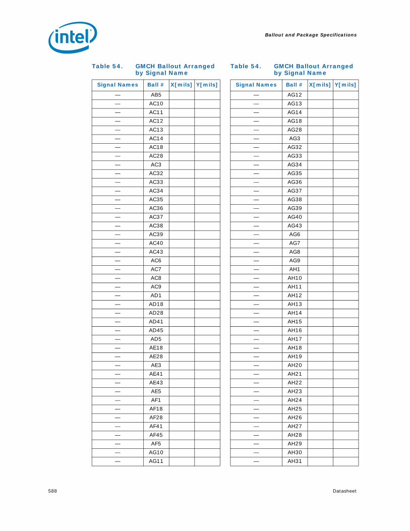
Ballout and Package Specifications
588 Datasheet
— AB5
— AC10
— AC11
— AC12
— AC13
— AC14
— AC18
— AC28
— AC3
— AC32
— AC33
— AC34
— AC35
— AC36
— AC37
— AC38
— AC39
— AC40
— AC43
— AC6
— AC7
— AC8
— AC9
— AD1
— AD18
— AD28
— AD41
— AD45
— AD5
— AE18
— AE28
— AE3
— AE41
— AE43
— AE5
— AF1
— AF18
— AF28
— AF41
— AF45
— AF5
— AG10
— AG11
Table 54. GMCH Ballout Arranged by Signal Name
Signal Names Ball # X[mils] Y[mils]
— AG12
— AG13
— AG14
— AG18
— AG28
— AG3
— AG32
— AG33
— AG34
— AG35
— AG36
— AG37
— AG38
— AG39
— AG40
— AG43
— AG6
— AG7
— AG8
— AG9
— AH1
— AH10
— AH11
— AH12
— AH13
— AH14
— AH15
— AH16
— AH17
— AH18
— AH19
— AH20
— AH21
— AH22
— AH23
— AH24
— AH25
— AH26
— AH27
— AH28
— AH29
— AH30
— AH31
Table 54. GMCH Ballout Arranged by Signal Name
Signal Names Ball # X[mils] Y[mils]

Ballout and Package Specifications
Datasheet 589
— AH32
— AH33
— AH34
— AH35
— AH36
— AH37
— AH38
— AH39
— AH40
— AH41
— AH45
— AH5
— AH6
— AH7
— AH8
— AH9
— AJ18
— AJ28
— AJ3
— AJ4
— AJ41
— AJ42
— AJ43
— AJ5
— AK1
— AK18
— AK28
— AK41
— AK45
— AK5
— AL13
— AL18
— AL28
— AL3
— AL33
— AL43
— AM1
— AM10
— AM11
— AM12
— AM13
— AM14
— AM18
Table 54. GMCH Ballout Arranged by Signal Name
Signal Names Ball # X[mils] Y[mils]
— AM19
— AM23
— AM27
— AM28
— AM32
— AM33
— AM34
— AM35
— AM36
— AM37
— AM38
— AM39
— AM40
— AM41
— AM45
— AM5
— AM6
— AM7
— AM8
— AM9
— AN1
— AN12
— AN14
— AN15
— AN18
— AN19
— AN2
— AN23
— AN27
— AN28
— AN3
— AN31
— AN32
— AN34
— AN4
— AN41
— AN42
— AN43
— AN44
— AN45
— AN5
— AP10
— AP11
Table 54. GMCH Ballout Arranged by Signal Name
Signal Names Ball # X[mils] Y[mils]

Ballout and Package Specifications
590 Datasheet
— AP12
— AP13
— AP14
— AP18
— AP19
— AP23
— AP27
— AP28
— AP3
— AP32
— AP33
— AP34
— AP35
— AP36
— AP37
— AP38
— AP39
— AP4
— AP40
— AP41
— AP42
— AP43
— AP5
— AP6
— AP7
— AP8
— AP9
— AR1
— AR12
— AR14
— AR18
— AR19
— AR23
— AR27
— AR28
— AR32
— AR34
— AR41
— AR45
— AR5
— AT10
— AT12
— AT14
Table 54. GMCH Ballout Arranged by Signal Name
Signal Names Ball # X[mils] Y[mils]
— AT18
— AT19
— AT23
— AT27
— AT28
— AT3
— AT32
— AT34
— AT36
— AT37
— AT38
— AT39
— AT4
— AT40
— AT41
— AT42
— AT43
— AT5
— AT6
— AT7
— AT8
— AT9
— AU1
— AU10
— AU12
— AU14
— AU18
— AU19
— AU23
— AU27
— AU28
— AU32
— AU34
— AU36
— AU45
— AV10
— AV12
— AV14
— AV18
— AV19
— AV23
— AV27
— AV28
Table 54. GMCH Ballout Arranged by Signal Name
Signal Names Ball # X[mils] Y[mils]

Ballout and Package Specifications
Datasheet 591
— AV3
— AV32
— AV34
— AV36
— AV41
— AV43
— AV5
— AW1
— AW10
— AW12
— AW14
— AW18
— AW19
— AW23
— AW27
— AW28
— AW32
— AW34
— AW36
— AW40
— AW41
— AW45
— AW5
— AW6
— AY10
— AY12
— AY14
— AY18
— AY19
— AY23
— AY27
— AY28
— AY3
— AY32
— AY34
— AY36
— AY39
— AY41
— AY43
— AY5
— AY7
— B1
— B13
Table 54. GMCH Ballout Arranged by Signal Name
Signal Names Ball # X[mils] Y[mils]
— B33
— B41
— B5
— BA1
— BA10
— BA11
— BA12
— BA13
— BA14
— BA16
— BA17
— BA18
— BA2
— BA20
— BA21
— BA22
— BA24
— BA25
— BA26
— BA28
— BA29
— BA30
— BA32
— BA33
— BA34
— BA35
— BA36
— BA38
— BA39
— BA4
— BA40
— BA42
— BA44
— BA45
— BA6
— BA7
— BA8
— BB1
— BB10
— BB12
— BB13
— BB17
— BB29
Table 54. GMCH Ballout Arranged by Signal Name
Signal Names Ball # X[mils] Y[mils]

Ballout and Package Specifications
592 Datasheet
— BB3
— BB33
— BB34
— BB36
— BB4
— BB41
— BB42
— BB43
— BB45
— BB5
— BC10
— BC12
— BC13
— BC15
— BC17
— BC19
— BC21
— BC23
— BC25
— BC27
— BC29
— BC31
— BC33
— BC34
— BC36
— BC38
— BC4
— BC40
— BC42
— BC6
— BC8
— BD13
— BD33
— BD41
— BD5
— BE11
— BE13
— BE14
— BE16
— BE18
— BE20
— BE22
— BE24
Table 54. GMCH Ballout Arranged by Signal Name
Signal Names Ball # X[mils] Y[mils]
— BE26
— BE28
— BE30
— BE32
— BE33
— BE35
— BE37
— BE39
— BE4
— BE41
— BE42
— BE5
— BE7
— BE9
— C10
— C12
— C13
— C15
— C17
— C19
— C21
— C23
— C25
— C27
— C29
— C31
— C33
— C34
— C36
— C38
— C4
— C40
— C42
— C6
— C8
— D1
— D10
— D12
— D13
— D17
— D29
— D3
— D33
Table 54. GMCH Ballout Arranged by Signal Name
Signal Names Ball # X[mils] Y[mils]

Ballout and Package Specifications
Datasheet 593
— D34
— D36
— D4
— D41
— D42
— D43
— D45
— D5
— E1
— E10
— E11
— E12
— E13
— E14
— E16
— E17
— E18
— E2
— E20
— E21
— E22
— E24
— E25
— E26
— E28
— E29
— E30
— E32
— E33
— E34
— E35
— E36
— E38
— E39
— E4
— E40
— E42
— E44
— E45
— E6
— E7
— E8
— F10
Table 54. GMCH Ballout Arranged by Signal Name
Signal Names Ball # X[mils] Y[mils]
— F12
— F14
— F18
— F19
— F23
— F27
— F28
— F3
— F32
— F34
— F36
— F39
— F41
— F43
— F5
— F7
— G1
— G10
— G12
— G14
— G18
— G19
— G23
— G27
— G28
— G32
— G34
— G36
— G40
— G41
— G45
— G5
— G6
— H10
— H12
— H14
— H18
— H19
— H23
— H27
— H28
— H3
— H32
Table 54. GMCH Ballout Arranged by Signal Name
Signal Names Ball # X[mils] Y[mils]

Ballout and Package Specifications
594 Datasheet
— H34
— H36
— H41
— H43
— H5
— J1
— J10
— J12
— J14
— J18
— J19
— J23
— J27
— J28
— J32
— J34
— J36
— J45
— K10
— K12
— K14
— K18
— K19
— K23
— K27
— K28
— K3
— K32
— K34
— K36
— K37
— K38
— K39
— K4
— K40
— K41
— K42
— K43
— K5
— K6
— K7
— K8
— K9
Table 54. GMCH Ballout Arranged by Signal Name
Signal Names Ball # X[mils] Y[mils]
— L1
— L12
— L14
— L18
— L19
— L23
— L27
— L28
— L32
— L34
— L41
— L45
— L5
— M10
— M11
— M12
— M13
— M14
— M18
— M19
— M23
— M27
— M28
— M3
— M32
— M33
— M34
— M35
— M36
— M37
— M38
— M39
— M4
— M40
— M41
— M42
— M43
— M5
— M6
— M7
— M8
— M9
— N1
Table 54. GMCH Ballout Arranged by Signal Name
Signal Names Ball # X[mils] Y[mils]

Ballout and Package Specifications
Datasheet 595
— N12
— N14
— N15
— N18
— N19
— N2
— N23
— N27
— N28
— N3
— N31
— N32
— N34
— N4
— N41
— N42
— N43
— N44
— N45
— N5
— P1
— P10
— P11
— P12
— P13
— P14
— P18
— P19
— P23
— P27
— P28
— P32
— P33
— P34
— P35
— P36
— P37
— P38
— P39
— P40
— P41
— P45
— P5
Table 54. GMCH Ballout Arranged by Signal Name
Signal Names Ball # X[mils] Y[mils]
— P6
— P7
— P8
— P9
— R13
— R18
— R28
— R3
— R33
— R43
— T1
— T18
— T28
— T41
— T45
— T5
— U18
— U28
— U3
— U4
— U41
— U42
— U43
— U5
— V1
— V10
— V11
— V12
— V13
— V14
— V15
— V16
— V17
— V18
— V19
— V20
— V21
— V22
— V23
— V24
— V25
— V26
— V27
Table 54. GMCH Ballout Arranged by Signal Name
Signal Names Ball # X[mils] Y[mils]

Ballout and Package Specifications
596 Datasheet
— V28
— V29
— V30
— V31
— V32
— V33
— V34
— V35
— V36
— V37
— V38
— V39
— V40
— V41
— V45
— V5
— V6
— V7
— V8
— V9
— W10
— W11
— W12
— W13
— W14
— W18
— W28
— W3
— W32
— W33
— W34
— W35
— W36
— W37
— W38
— W39
— W40
— W43
— W6
— W7
— W8
— W9
— Y1
Table 54. GMCH Ballout Arranged by Signal Name
Signal Names Ball # X[mils] Y[mils]
— Y18
— Y28
— Y41
— Y45
— Y5
Table 54. GMCH Ballout Arranged by Signal Name
Signal Names Ball # X[mils] Y[mils]

Datasheet 597
Ballout and Package Specifications
15.2 Package Specifications
The (G)MCH is available in a 34 mm [1.34 in] x 34 mm [1.34 in] Flip Chip Ball Grid Array (FC-BGA) package with 1254 solder balls (see Figure 21). Refer to the Intel® 4 Series Chipset Family Thermal and Mechanical Design Guide for details.
§ §
Figure 21. (G)MCH Package Drawing

Ballout and Package Specifications
598 Datasheet

Datasheet 599
Testability
16 Testability
In the (G)MCH, testability for Automated Test Equipment (ATE) board level testing has been implemented as both JTAG boundary scan and XOR chains.
16.1 JTAG Boundary Scan
The (G)MCH adds Boundary Scan ability compatible with the IEEE 1149.1-2001 Standard (Test Access Port and Boundary-Scan Architecture) specification. Refer to the above mentioned specification for functionality. See Figure 22 for test mode entry.
The BSCANTEST pin serves as a boundary-scan test strap. Assertion of this strap (low) is required to disable glitch-masking logic; otherwise, boundary-scan control signals to device pin are blocked.
The DDR3_DRAM_PWROK pin must be high for the ddr3_dramrstb pin boundary-scan data to become valid. Note that this signal is only used on platforms where DDR3 is enabled. On DDR2 platforms, if DDR3_DRAM_PWROK is held low, then the boundary-scan data on the ddr3_dramrstb pin will be invalid.
Figure 22. JTAG Boundary Scan Test Mode Initialization Cycles
bscantestddpc_ctrldatasdvo_ctrldata
ddr3_dram_pwrok
cl_pwrok
pwrok
cl_rstb
rstinb
hpl_clkinpexp_clkp
hpl_clkinn exp_clkn
= 3 cycles
jtag_tck
jtag_tms
clock running or stopped
= 0 µs
= 1 µs
= 3 µs
clock running or stopped
(Clock frequency not critical)
= 1 µs
= 1 cycle
= 1 µs = 5 cycles
drive straps low (values not important here)

Testability
600 Datasheet
The CL_PWROK pin provides hardware reset to the TAP, so it must be driven low at power up to ensure clean reset to the TAP. This pin must be driven high to indicate that power is valid, which also allows the TAP to come out of reset.
CL_RSTB must be high for the specified time, for fuses to be loaded and valid before PWROK is asserted.
The PWROK pin must be driven high in order to indicate that power is valid. It also latches the BSCANTEST strap.
The RSTINB pin must be initially active (low) then de-asserted (high) so that the I/O buffers will operate correctly.
Clocking of the HPL_CLKINN/P and EXP_CLKN/P pins is required to initialize internal registers including those that set default buffer compensation values. Clock frequency is not critical due to PLL bypass mode forced when bscantest strap is asserted.
The JTAG_TMS pin should be held high before asserting MEPWROK (CL_PWROK), and held high for at least 5 JTAG_TCK cycles to ensure that the TAP exits the Test-Logic-Reset state at the expected time once TMS goes low. Note that JTAG_TMS has an internal pullup.
16.1.1 TAP Instructions and Opcodes
The TAP controller supports the JTAG instructions as listed in Table 55. The instruction register length is 4 bits.
16.1.2 TAP interface and timings.
The (G)MCH uses 4 dedicated pins to access the Test Access Port (TAP), and the port timings are shown in Figure 23.
Table 55. Supported TAP Instructions
Opcode(binary)
InstructionSelected Test Data
RegisterTDR Length
0000b EXTEST Boundary-scan 485
0001bSAMPLE/PRELOAD (SAMPRE)
Boundary-scan 485
0011b IDCODEDevice Identification (value: 0x04105013)
32
0100b CLAMP Bypass 1
0101b EXTEST_TOGGLE Boundary-scan 485
0110b HIGHZ Bypass 1
1111b BYPASS Bypass 1
others Reserved

Datasheet 601
Testability
Table 56. JTAG Pins
Pin Direction Description
JTAG_TCK Input Test clock pin for JTAG TAP Controller and test logic
JTAG_TMSInput with weak pullup
JTAG Test Mode Select pin. Sampled by the TAP on the Rising edge of TCK to control the operation of the TAP state machine. It is recommended that TMS is held high when (CL_PWROK) is driven from low-to-high, to ensure deterministic operation of the test logic.
JTAG_TDIInput with weak pullup
JTAG Test Data Input pin, sampled on the Rising edge of TCK to provide serial test instructions and data.
JTAG_TDO OutputJTAG Test Data Output pin. In inactive drive state except when instructions or data are being shifted. TDO changes on the falling edge of TCK. During shifting, TDO drives actively high and low.
Figure 23. JTAG Test Mode Initialization Cycles
T C K
T M ST D I
T D O
T JC T JC H
T J SU T JH
T JC O T JC O T J VZ
T J C L
Table 57. JTAG Signal Timings
Symbol Parameter Min Max Unit Notes
TJC JTAG TCK clock period 25 — ns 40 MHZ
TJCL JTAG TCK clock low time 0.4 * TJC — ns
TJCH JTAG TCK clock high time 0.4 * TJC — ns
TJSU Setup of TMS and TDI before TCK rising 11 — ns
TJH TMS and TDI hold after TCK rising 5 — ns
TJCO TCK falling to TDO output valid — 7 ns
TJVZ TCK falling to TDO output high-impedance — 9 ns

Testability
602 Datasheet
16.2 XOR Test Mode Initialization
An XOR-tree is a chain of XOR gates each with one input pin connected to it, which allows for pad to ball to trace connection testing.
The XOR testing methodology is to boot the part using straps to enter XOR mode (A description of the boot process follows). Once in XOR mode, all of the pins of an XOR chain are driven to logic 1. This action will force the output of that XOR chain to either a 1 if the number of the pins making up the chain is even or a 0 if the number of the pins making up the chain is odd.
Once a valid output is detected on the XOR chain output, a walking 0 pattern is moved from one end of the chain to the other. Every time the walking 0 is applied to a pin on the chain, the output will toggle. If the output does not toggle, there is a disconnect somewhere between die, package, and board and the system can be considered a failure.
Figure 24 shows the wave forms to be able to boot the (G)MCH into XOR mode. The straps that need to be controlled during this boot process are BSEL[2:0], SDVO_CTRLDATA, EXP_EN, EXP_SLR, and XORTEST.
All strap values must be driven before PWROK asserts. BSEL0 must be a 1. BSEL[2:1] need to be defined values, but logic value in any order will work. XORTEST must be driven to 0.
Figure 24. XOR Test Mode Initialization Cycles
PWROK
RSTIN#
STRAP PINS
HCLKP/GCLKP
HCLKN/GCLKN
XOR inputs
XOR output
CL_PWROK
X
CL_RST#
Datasheet 603
Testability
If sDVO is present in the design, SDVO_CTRLDATA must be pulled to logic 1. Depending on if Static Lane Reversal is used and if the sDVO/PCIe Coexistence is selected, EXP_SLR and EXP_EN must be pulled in a valid manner.
16.2.1 XOR Chain Definition
For the (G)MCH XOR chain definitions, contact your Intel field representative.
§ §

Testability
604 Datasheet


