Memory testing.1
Memory Testing
• Introduction• Memory Architecture & Fault Models• Test Algorithms• DC / AC / Dynamic Tests• Built-in Self Testing Schemes• Built-in Self Repair Schemes
Memory testing.2
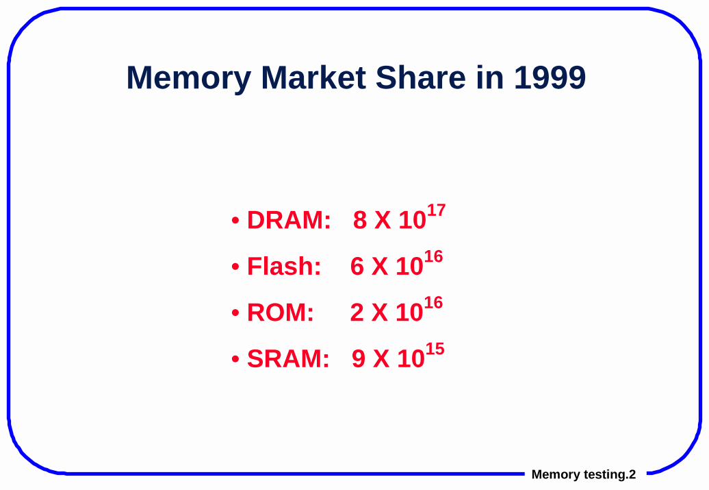
Memory Market Share in 1999
• DRAM: 8 X 10¹⁷
• Flash: 6 X 10¹⁶
• ROM: 2 X 10¹⁶
• SRAM: 9 X 10¹⁵

Memory testing.3
DRAM Price per Bit
1991: US$ 400 / Mega bits
1995: US$ 3.75 / Mega bits
1999: US$ 0.1~0.3 / Mega bits
Memory testing.4
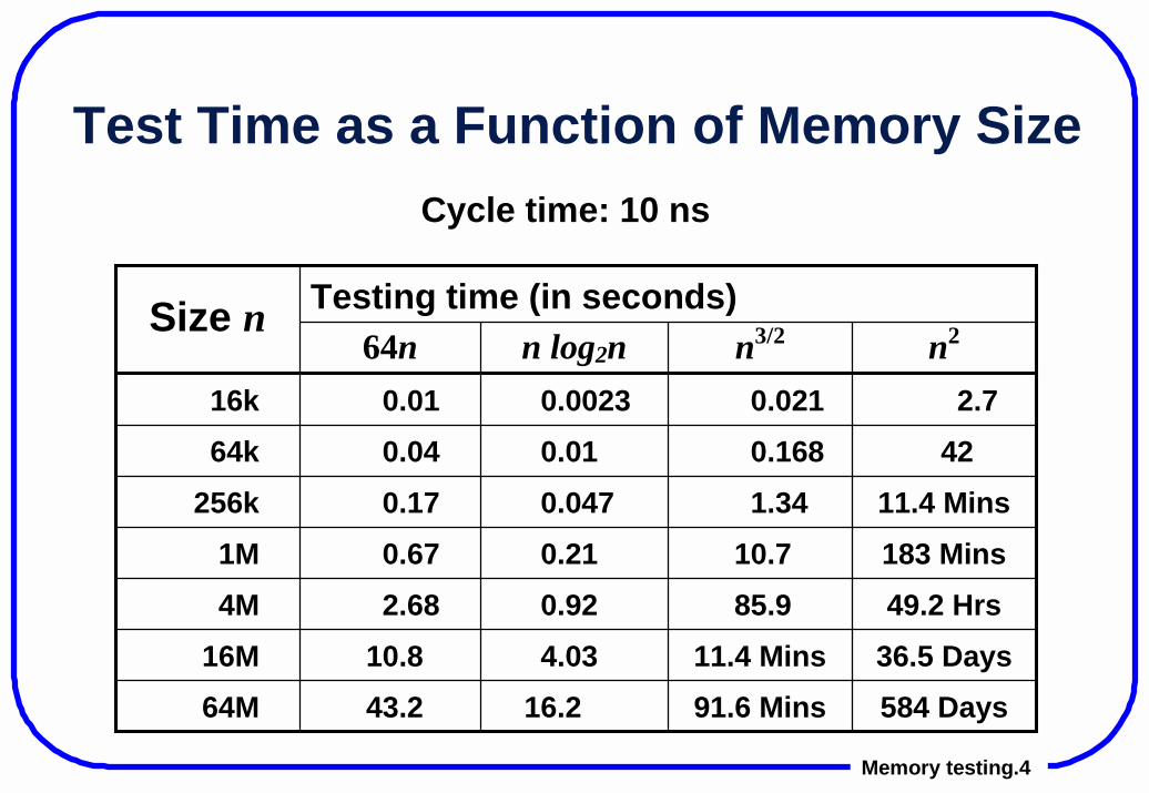
Test Time as a Function of Memory SizeCycle time: 10 ns
584 Days91.6 Mins16.243.264M36.5 Days11.4 Mins4.0310.816M49.2 Hrs85.90.922.684M183 Mins10.70.210.671M11.4 Mins1.340.0470.17256k
420.1680.010.0464k2.70.0210.00230.0116k
n2n3/2n log2n64nTesting time (in seconds)Size n
Memory testing.5
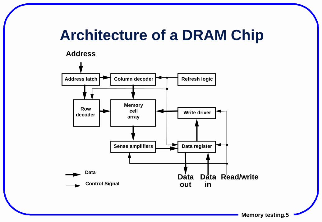
Architecture of a DRAM Chip
Read/write
Address latch Column decoder
Memory cell
arrayRow
decoder
Refresh logic
Write driver
Data registerSense amplifiers
Address
Data out
Data in
Data
Control Signal
Memory testing.6
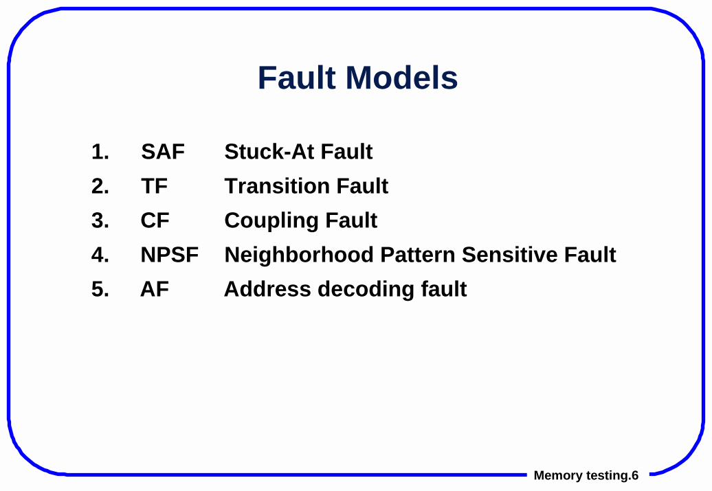
Fault Models
1. SAF Stuck-At Fault2. TF Transition Fault3. CF Coupling Fault4. NPSF Neighborhood Pattern Sensitive Fault5. AF Address decoding fault
Memory testing.7
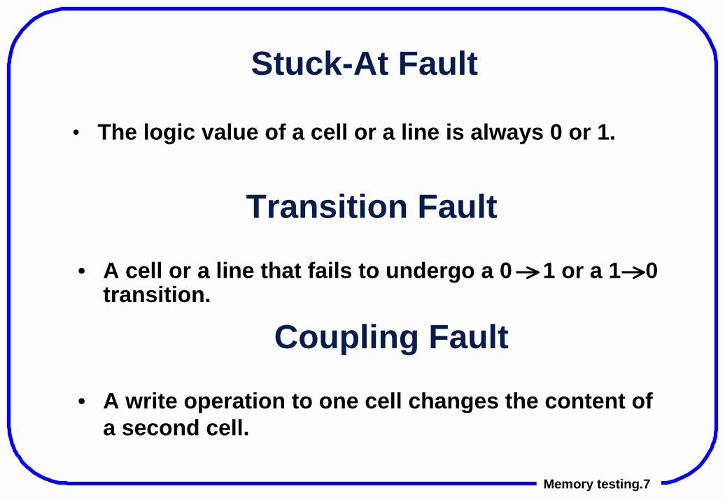
Stuck-At Fault
• The logic value of a cell or a line is always 0 or 1.
Transition Fault
• A cell or a line that fails to undergo a 0 1 or a 1 0transition.
Coupling Fault
• A write operation to one cell changes the content ofa second cell.
Memory testing.8
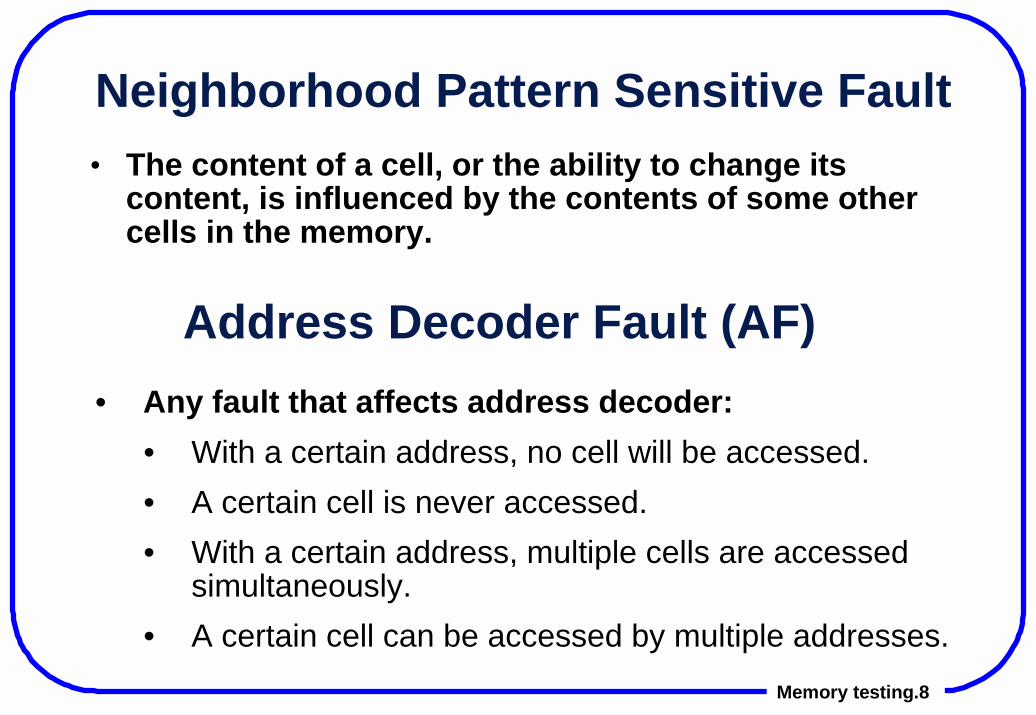
Neighborhood Pattern Sensitive Fault• The content of a cell, or the ability to change its
content, is influenced by the contents of some othercells in the memory.
• Any fault that affects address decoder:• With a certain address, no cell will be accessed.• A certain cell is never accessed.• With a certain address, multiple cells are accessed
simultaneously.• A certain cell can be accessed by multiple addresses.
Address Decoder Fault (AF)

Memory testing.9
Memory Chip Test Algorithms• Traditional tests• Tests for stuck-at, transition and coupling faults• Tests for neighborhood pattern sensitive faults

Memory testing.10
Traditional Tests Algorithm Test length Test Time Order
• Zero-One• Checkerboard• GALPAT • Walking 1/0• Sliding Diagonal• Butterfly
• n is the number of bits of the memory array.
��� ⋅+��
�������� −+ ���
��� ���+���� �
��+
��
��
����
����
�� ���
�� ���
�� ��� ⋅�� ��
���� ⋅
Memory testing.11
March Algorithms
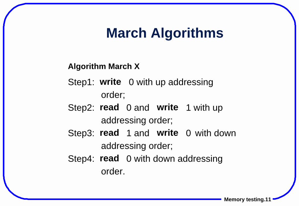
Algorithm March X
Step1: write 0 with up addressing order;
Step2: read 0 and write 1 with up addressing order;
Step3: read 1 and write 0 with down addressing order;
Step4: read 0 with down addressing order.
Memory testing.12
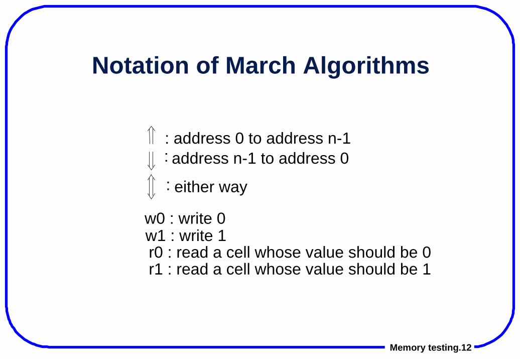
Notation of March Algorithms
: address 0 to address n-1: address n-1 to address 0
w0 : write 0w1 : write 1r0 : read a cell whose value should be 0r1 : read a cell whose value should be 1
: either way

Memory testing.13
March Algorithms
EX:MATS ( modified algorithmic Test Sequence)
s1: write 0 to all cellss2: for each cell
read 0 ; write 1;
s3: read 1 from all cells
(w0); (r0,w1); (r1);

Memory testing.14
Some March Algorithms
MATS : (w0); (r0,w1); (r1)MATS+: (w0); (r0,w1); (r1,w0)Marching 1/0 : (w0); (r0,w1,r1); (r1,w0,r0);
(w1); (r1,w0,r0); (r0, w1, r1);
MATS++ : (w0); (r0,w1); (r1,w0,r0);MARCH X : (w0); (r0,w1); (r1,w0); (r0)MARCH C : (w0); (r0,w1); (r1,w0); (r0);
(r0,w1); (r1,w0); (r0);
Memory testing.15
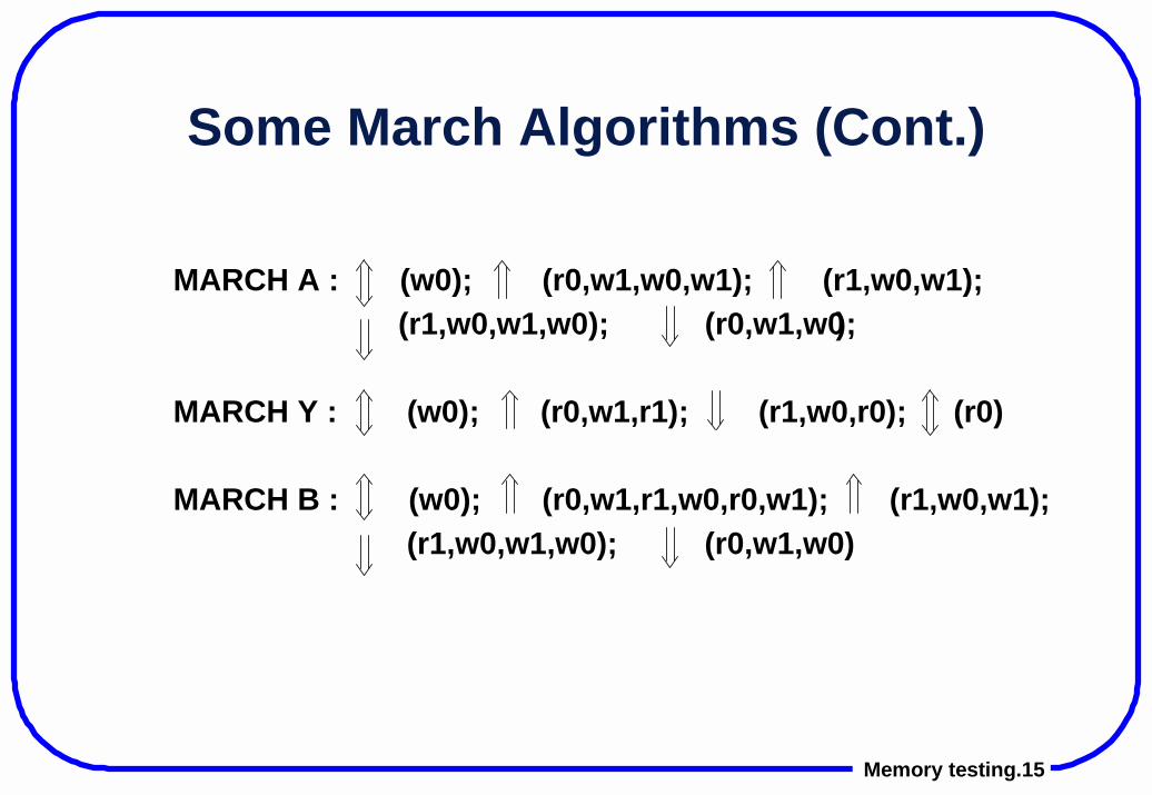
Some March Algorithms (Cont.)
MARCH A : (w0); (r0,w1,w0,w1); (r1,w0,w1); (r1,w0,w1,w0); (r0,w1,w0);
MARCH Y : (w0); (r0,w1,r1); (r1,w0,r0); (r0)
MARCH B : (w0); (r0,w1,r1,w0,r0,w1); (r1,w0,w1);(r1,w0,w1,w0); (r0,w1,w0 )
Memory testing.16
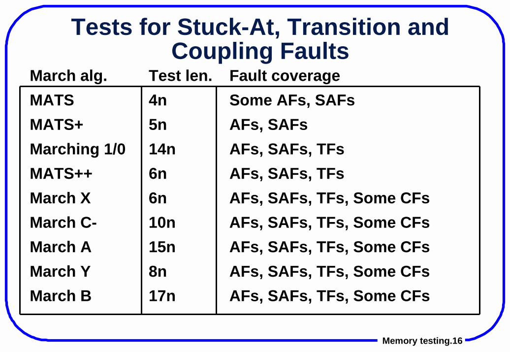
Tests for Stuck-At, Transition andCoupling Faults
March alg. Test len. Fault coverageMATS 4n Some AFs, SAFsMATS+ 5n AFs, SAFsMarching 1/0 14n AFs, SAFs, TFsMATS++ 6n AFs, SAFs, TFsMarch X 6n AFs, SAFs, TFs, Some CFsMarch C- 10n AFs, SAFs, TFs, Some CFsMarch A 15n AFs, SAFs, TFs, Some CFsMarch Y 8n AFs, SAFs, TFs, Some CFsMarch B 17n AFs, SAFs, TFs, Some CFs
Memory testing.17
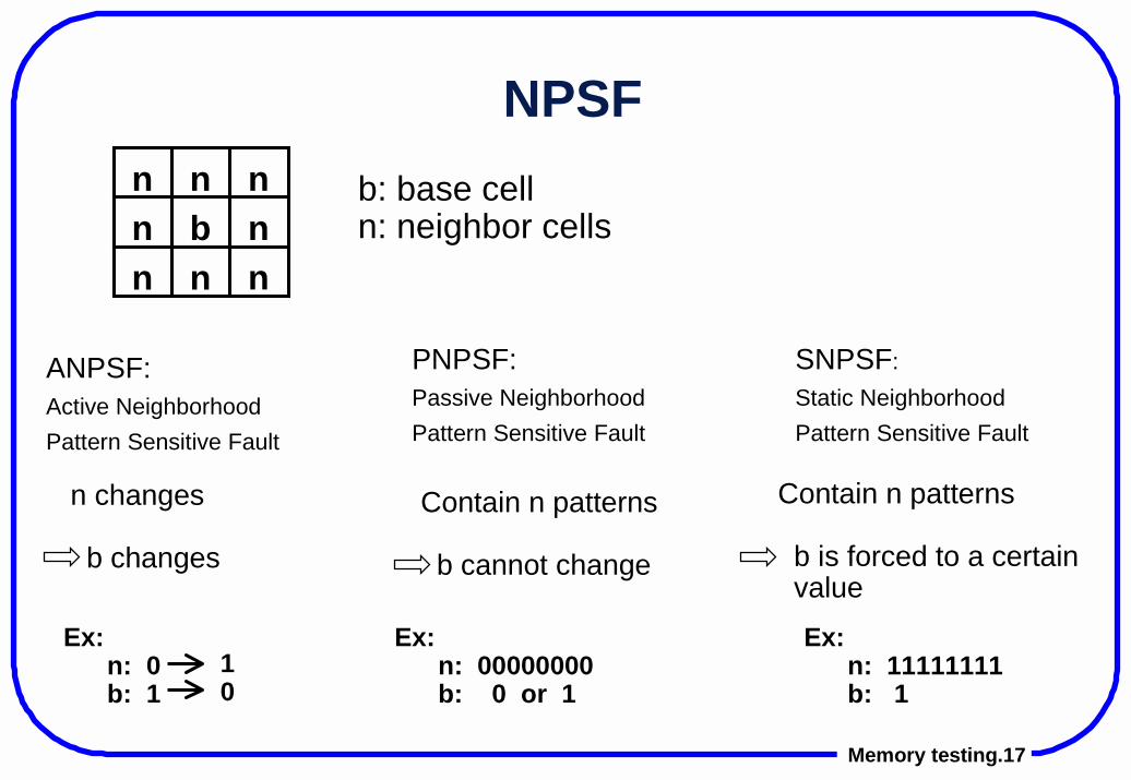
NPSFn n nn b nn n n
b: base celln: neighbor cells
ANPSF: Active Neighborhood Pattern Sensitive Fault
n changes b changes
PNPSF: Passive Neighborhood Pattern Sensitive Fault
SNPSF: Static Neighborhood Pattern Sensitive Fault
Contain n patterns b cannot change
Contain n patterns b is forced to a certain value
Ex: n: 0 b: 1
10
Ex: n: 00000000 b: 0 or 1
Ex: n: 11111111 b: 1
Memory testing.18
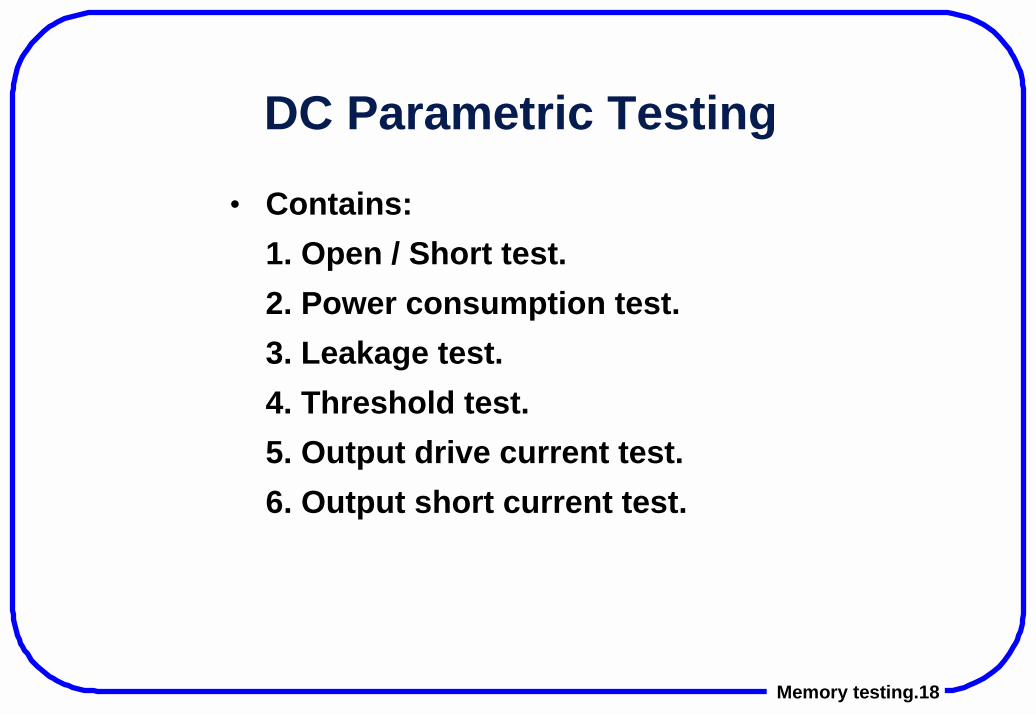
DC Parametric Testing
• Contains:1. Open / Short test.2. Power consumption test.3. Leakage test.4. Threshold test.5. Output drive current test.6. Output short current test.
Memory testing.19
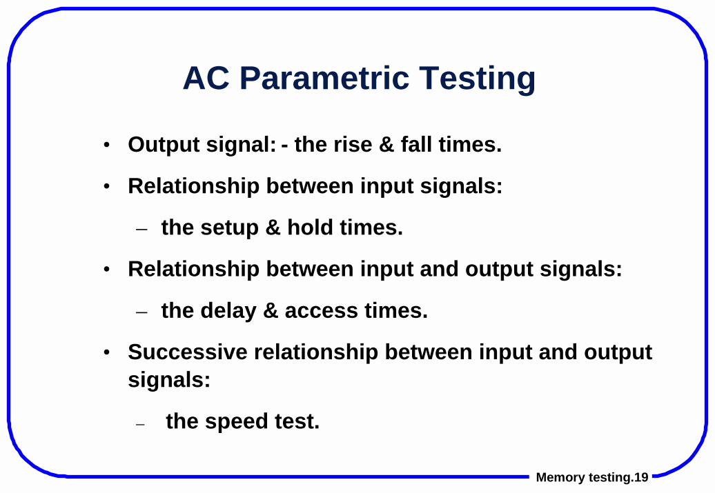
AC Parametric Testing
• Output signal: - the rise & fall times.
• Relationship between input signals:
– the setup & hold times.
• Relationship between input and output signals:
– the delay & access times.
• Successive relationship between input and outputsignals:
– the speed test.

Memory testing.20
Dynamic Faults• Recovery faults:
− Sense amplifier recovery− Write recovery.
− Retention faults:− Sleeping sickness− Refresh line stuck-at− Static data loss.
− Bit-line precharge voltage imbalance faults.
Memory testing.21
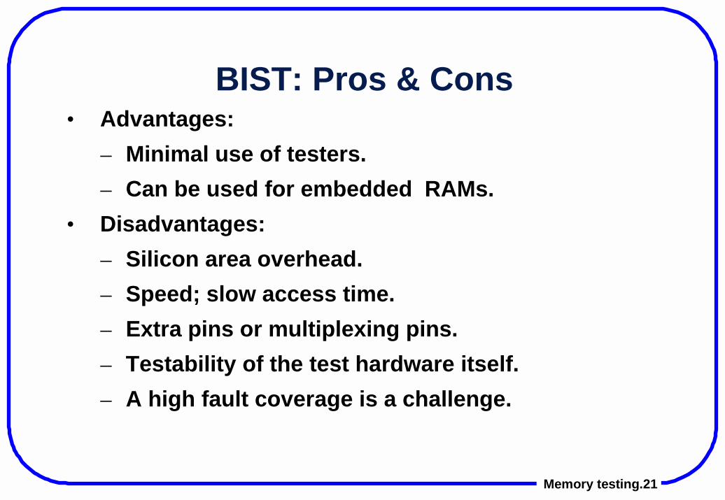
BIST: Pros & Cons• Advantages:
– Minimal use of testers.– Can be used for embedded RAMs.
• Disadvantages:– Silicon area overhead.– Speed; slow access time.– Extra pins or multiplexing pins.– Testability of the test hardware itself.– A high fault coverage is a challenge.
Memory testing.22
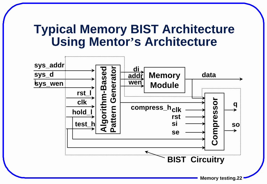
Typical Memory BIST ArchitectureUsing Mentor’s Architecture
BIST Circuitry
MemoryModule
Alg
orith
m-B
ased
Patte
rn G
ener
ator
Com
pres
sor
diaddrwen
data
compress_h
sys_addrsys_disys_wen
rst_lclk
hold_ltest_h
q
so
clkrstsise
Memory testing.23
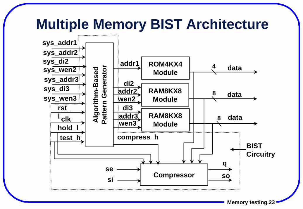
Multiple Memory BIST Architecture
ROM4KX4Module
addr1 data
compress_h
sys_addr1
sys_di2sys_wen2
rst_l clkhold_ltest_h
Compressorq
sosise
RAM8KX8Module
di2addr2wen2 data
RAM8KX8Module
di3addr3wen3
data
BISTCircuitry
Alg
orith
m-B
ased
Patte
rn G
ener
ator
sys_addr3
sys_addr2
sys_wen3sys_di3
4
8
8
Memory testing.24
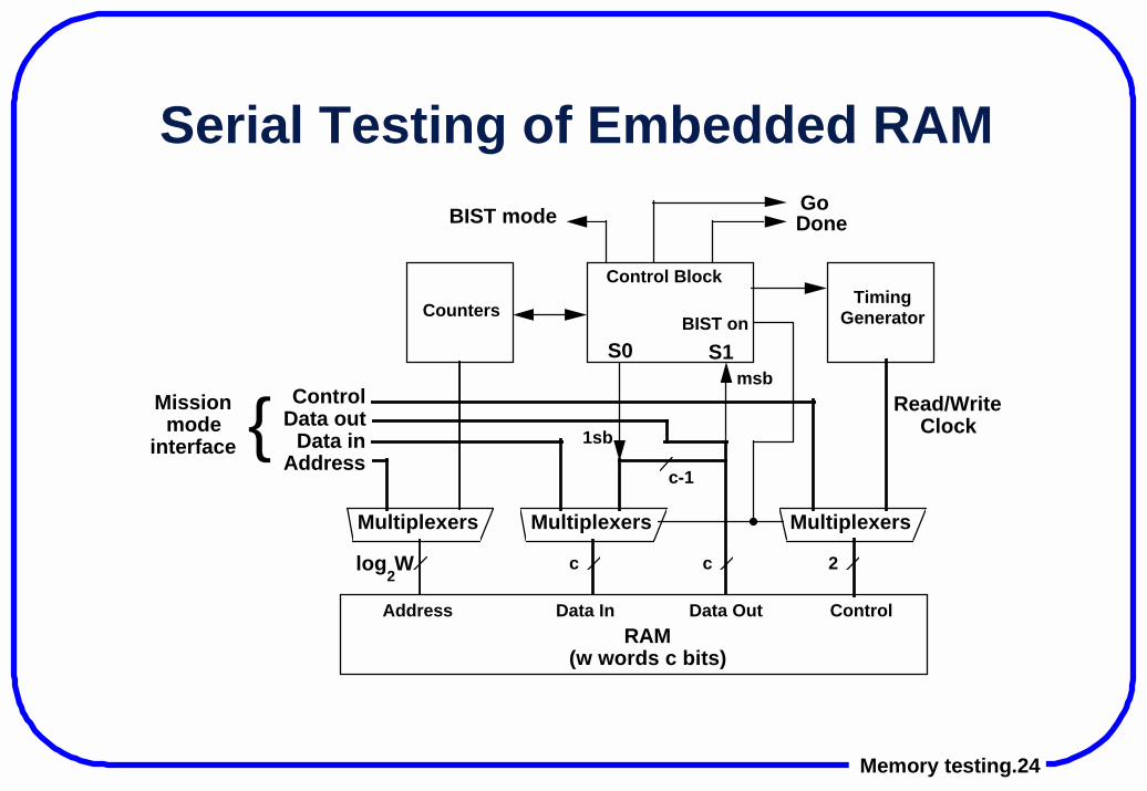
Serial Testing of Embedded RAMBIST mode
Counters
Go
c
Address
W
Control Data out
Data in Address
RAM (w words c bits)
Multiplexers
log2
Multiplexers
Data In Data Out Control
2
Multiplexers
c-1
1sb
Control Block
BIST onS0 S1
msb
c
Done
Timing Generator
Read/Write Clock{Mission
mode interface

Memory testing.25
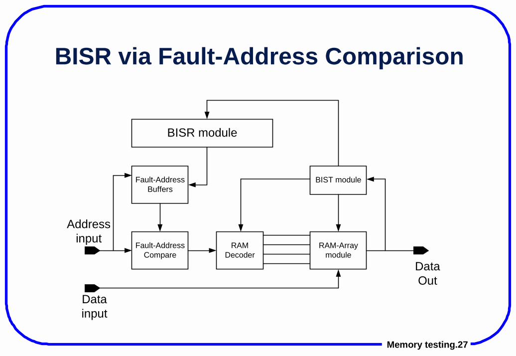
Built-in Self-Repair
• BIST can only identify faulty chip.• Laser cut may be infeasible in some cases, e.g., field
testing.• Two types:
– Use fault-array comparator! Repair by cell! Repair by column (or row)
– Use switch array
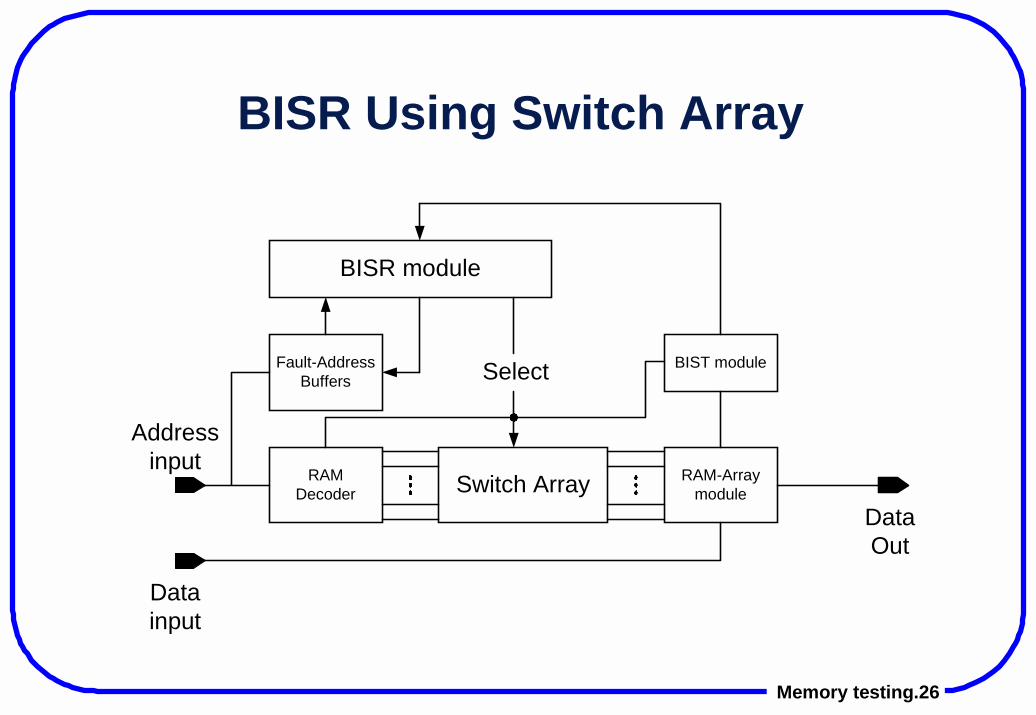
Memory testing.26
BISR Using Switch Array
BISR module
Fault-AddressBuffers
RAMDecoder
RAM-Arraymodule
BIST module
Switch Array
Select
DataOut
Addressinput
Datainput
Memory testing.27
BISR via Fault-Address Comparison
BISR module
Fault-AddressBuffers
Fault-AddressCompare
RAMDecoder
RAM-Arraymodule
BIST module
Addressinput
Datainput
DataOut


