
L10 Quectel GPS Engine
Hardware Design L10_Hardware_Design_V1.1

L10 Hardware Design
L10_Hardware_Design_V1.1 - 1 -
Document Title L10 Hardware Design
Revision 1.1
Date 2009-11-16
Status Release
Document Control ID L10_Hardware_Design_V1.1
General Notes
Quectel offers this information as a service to its customers, to support application and
engineering efforts that use the products designed by Quectel. The information provided is
based upon requirements specifically provided for Quectel by the customers. Quectel has not
undertaken any independent search for additional relevant information, including any
information that may be in the customer’s possession. Furthermore, system validation of this
product designed by Quectel within a larger electronic system remains the responsibility of
the customer or the customer’s system integrator. All specifications supplied herein are
subject to change.
Copyright
This document contains proprietary technical information which is the property of Quectel
Limited, copying of this document and giving it to others and the using or communication of
the contents thereof, are forbidden without express authority. Offenders are liable to the
payment of damages. All rights reserved in the event of grant of a patent or the registration of
a utility model or design. All specification supplied herein are subject to change without
notice at any time.
Copyright © Quectel Wireless Solutions Co., Ltd. 2009
Quectel
Confidential

L10 Hardware Design
L10_Hardware_Design_V1.1 - 2 -
Contents
0 Revision history .......................................................................................................... 6
1 Introduction ................................................................................................................. 7
1.1 Related documents ............................................................................................................... 7
1.2 Terms and abbreviations ....................................................................................................... 7
2 Product concept ........................................................................................................... 9
2.1 Key features ......................................................................................................................... 9
2.2 Functional diagram ............................................................................................................. 10
2.3 Evaluation board ................................................................................................................ 11
2.4 Assisted GPS ...................................................................................................................... 11
2.5 Protocol .............................................................................................................................. 11
3 Application interface ................................................................................................. 12
3.1 Pin description .................................................................................................................... 12
3.2 Operating modes ................................................................................................................ 14
3.3 Power supply ...................................................................................................................... 14
3.4 Turn on and Turn off .......................................................................................................... 14
3.4.1 Turn on ..................................................................................................................... 14
3.4.2 Turn off..................................................................................................................... 16
3.5 Power saving ...................................................................................................................... 16
3.5.1 Enter standby mode .................................................................................................. 16
3.5.2 Exit from standby mode ........................................................................................... 16
3.6 RTC backup ....................................................................................................................... 16
3.7 UART interface .................................................................................................................. 18
3.8 USB interface ..................................................................................................................... 20
3.9 Software upgrade................................................................................................................ 21
3.10 EXTINT0 ......................................................................................................................... 21
3.11 AOK ................................................................................................................................. 21
3.12 I2C interface ..................................................................................................................... 22
4 Antenna interface and supervisor ............................................................................. 23
4.1 Antenna .............................................................................................................................. 23
4.2 Antenna supply ................................................................................................................... 24
4.2.1 Passive antenna ......................................................................................................... 24
4.2.2 Active antenna .......................................................................................................... 25
5 Electrical, reliability and radio characteristics .......................................................... 27
5.1 PIN assignment of the module ........................................................................................... 27
5.2 Absolute maximum ratings ................................................................................................. 28
5.3 Operating conditions .......................................................................................................... 28
5.4 Current consumption .......................................................................................................... 29
5.5 Electro-static discharge ...................................................................................................... 29
5.6 Reliability test .................................................................................................................... 30
6 Mechanics ................................................................................................................. 31
Quectel
Confidential

L10 Hardware Design
L10_Hardware_Design_V1.1 - 3 -
6.1 Mechanical dimensions of the module ............................................................................... 31
6.2 Footprint of recommendation ............................................................................................. 33
6.3 Top view of the module ..................................................................................................... 35
6.4 Bottom view of the module ................................................................................................ 35
Quectel
Confidential

L10 Hardware Design
L10_Hardware_Design_V1.1 - 4 -
Table Index
TABLE 1: RELATED DOCUMENTS ..................................................................................................... 7
TABLE 2: TERMS AND ABBREVIATIONS ......................................................................................... 7
TABLE 3: MODULE KEY FEATURES .................................................................................................. 9
TABLE 4: THE MODULE SUPPORTS PROTOCOL .......................................................................... 11
TABLE 5: PIN DESCRIPTION ............................................................................................................. 12
TABLE 6: OVERVIEW OF OPERATING MODES.............................................................................. 14
TABLE 7: PIN DEFINITION OF THE V_BCKP PIN .......................................................................... 17
TABLE 8: PIN DEFINITION OF THE UART INTERFACES.............................................................. 18
TABLE 9: PIN DEFINITION OF USB INTERFACE ........................................................................... 20
TABLE 10: PIN DEFINITION OF THE EXTINT0 .............................................................................. 21
TABLE 11: PIN DEFINITION OF THE AOK ...................................................................................... 21
TABLE 12: PIN DEFINITION OF THE I2C INTERFACE .................................................................. 22
TABLE 13: PIN DEFINITION OF THE AADET_N ............................................................................. 23
TABLE 14: AADET_N AND ACTIVE ANTENNA.............................................................................. 24
TABLE 15: ANTENNA SPECIFICATION FOR L10 MODULE .......................................................... 24
TABLE 16: L10 PIN ASSIGNMENT .................................................................................................... 27
TABLE 17: ABSOLUTE MAXIMUM RATINGS................................................................................. 28
TABLE 18: THE MODULE POWER SUPPLY RATINGS ................................................................... 28
TABLE 19: THE MODULE CURRENT CONSUMPTION (PASSIVE ANTENNA) .......................... 29
TABLE 20: THE ESD ENDURANCE TABLE (TEMPERATURE: 25℃, HUMIDITY: 45 %) ........... 30
TABLE 21: RELIABILITY TEST ......................................................................................................... 30 Quectel
Confidential
L10 Hardware Design
L10_Hardware_Design_V1.1 - 5 -
Figure Index
FIGURE 1: MODULE FUNCTIONAL DIAGRAM ............................................................................. 11
FIGURE 2: REFERENCE RESET CIRCUIT USING OC CIRCUIT ................................................... 15
FIGURE 3: REFERENCE RESET CIRCUIT USING BUTTON .......................................................... 15
FIGURE 4: TIMING OF RESTART SYSTEM ..................................................................................... 16
FIGURE 5: RTC SUPPLY FROM NON-CHARGEABLE BATTERY OR CAPACITOR .................... 17
FIGURE 6: REFERENCE CHARGING CIRCUIT FOR CHARGEABLE BATTERY ........................ 17
FIGURE 7: SEIKO XH414H-IV01E CHARGE CHARACTERISTIC ................................................. 18
FIGURE 8: CONNECTION OF SERIAL INTERFACES ..................................................................... 19
FIGURE 9: RS-232 LEVEL SHIFT CIRCUIT ...................................................................................... 20
FIGURE 10: USB INTERFACE CIRCUIT ........................................................................................... 21
FIGURE 11: EXTERNAL DETECT CIRCUIT FOR OPEN-CIRCUIT OF ACTIVE ANTENNA ...... 23
FIGURE 12: REFERENCE DESIGN FOR PASSIVE ANTENNA ....................................................... 24
FIGURE 13: ACTIVE ANTENNA BIASING ....................................................................................... 25
FIGURE 14: ACTIVE ANTENNA WITH VCC_RF ............................................................................. 25
FIGURE 15: ACTIVE ANTENNA WITH EXTERNAL LDO .............................................................. 26
Quectel
Confidential

L10 Hardware Design
L10_Hardware_Design_V1.1 - 6 -
0 Revision history
Revision Date Author Description of change
1.0 2009-07-05 Yong AN/Samuel HONG Initial
1.1 2009-11-16 Yong AN/Samuel HONG 1. Add NMEA message type of module
output in default.
2. Add descriptions about relation
between USB interface and standby
mode.
Quectel
Confidential

L10 Hardware Design
L10_Hardware_Design_V1.1 - 7 -
1 Introduction
This document defines and specifies the L10 GPS module. It describes L10 hardware interface and its
external application reference circuits, mechanical size and air interface.
This document can help you quickly understand module interface specifications, electrical and
mechanical details. With the help of this document and other application notes, you can use L10 module
to design and set up your applications quickly.
1.1 Related documents
Table 1: Related documents
SN Document name Remark
[1] L10_HD_AN L10 Hardware Design Application Notes
[2] L10_EVB _UGD L10 EVB User Guide
[3] L10_GPS_Protocol L10 GPS Protocol Specification
1.2 Terms and abbreviations
Table 2: Terms and abbreviations
Abbreviation Description
BEE Broadcast Ephemeris Extension
EMC Electromagnetic Compatibility
ESD Electrostatic Discharge
EPO Extended Prediction Orbit
EGNOS, European Geostationary Navigation Overlay Service
GPS Global Positioning System
GNSS Global Navigation Satellite System
GGA GPS Fix Data
GLL Geographic Position – Latitude/Longitude
GSA GNSS DOP and Active Satellites
GSV GNSS Satellites in View
HDOP Horizontal Dilution of Precision
IC Integrated Circuit
I/O Input/Output
Kbps Kilo Bits Per Second
LNA Low Noise Amplifier
Quectel
Confidential

L10 Hardware Design
L10_Hardware_Design_V1.1 - 8 -
MSAS Multi-Functional Satellite Augmentation System
NMEA National Marine Electronics Association
OMA Open Mobile Alliance
PDOP Position Dilution of Precision
PMTK MTK Private Protocol
RMC Recommended Minimum Specific GNSS Data
RTCM Radio Technical Commission for Maritime Services
SBAS Satellite-based Augmentation System
SUPL Secure User Plane Location
SAW Surface Acoustic Wave
USB Universal Serial Bus
UART Universal Asynchronous Receiver & Transmitter
VDOP Vertical Dilution of Precision
VTG Course over Ground and Ground Speed, Horizontal Course and Horizontal
Velocity
WAAS Wide Area Augmentation System
ZDA Time & Date
Inorm Normal Current
Imax Maximum Load Current
Vmax Maximum Voltage Value
Vnorm Normal Voltage Value
Vmin Minimum Voltage Value
VIHmax Maximum Input High Level Voltage Value
VIHmin Minimum Input High Level Voltage Value
VILmax Maximum Input Low Level Voltage Value
VILmin Minimum Input Low Level Voltage Value
VImax Absolute Maximum Input Voltage Value
VImin Absolute Minimum Input Voltage Value
VOHmax Maximum Output High Level Voltage Value
VOHmin Minimum Output High Level Voltage Value
VOLmax Maximum Output Low Level Voltage Value
VOLmin Minimum Output Low Level Voltage Value
Quectel
Confidential

L10 Hardware Design
L10_Hardware_Design_V1.1 - 9 -
2 Product concept
The L10 GPS module brings the high performance of the MTK positioning engine to the industrial
standard. The module supports 210 PRN channels. With 66 search channels and 22 simultaneous
tracking channels, it acquires and tracks satellites in the shortest time even at indoor signal level. This
versatile, stand-alone receiver combines an extensive array of features with flexible connectivity
options. The embedded FLASH memory provides capacity for storing user-specific configuration
settings and allows for future updates. L10 advanced jamming suppression mechanism and innovative
RF architecture provides a high level of immunity for jamming, ensuring maximum GPS performance.
The module supports location, navigation and industrial applications including autonomous GPS C/A,
SBAS (including WAAS, EGNOS, MSAS), DGPS (RTCM), and AGPS.
The L10 is an SMD type module with the compact 22.4mm x 17.0mm x 3.0 mm form factor, which can
be embedded in customer applications through the 28-pin pads. It provides all hardware interfaces
between the module and customer’s board.
The UART port can help to develop customer’s application easily.
The USB port is available for faster data transmission and more flexibility
The antenna interface supports passive and active antenna.
The module is fully RoHS compliant to EU regulation.
2.1 Key features
Table 3: Module key features
Feature Implementation
Power supply Single supply voltage: 3.0V – 4.3V typical : 3.3V
Power consumption
(passive antenna)
Acquisition 43mA
Tracking 38mA
Standby 2mA
Receiver Type GPS L1 1575.42MHz C/A Code
66 search channels, 22 simultaneous tracking channels
Sensitivity Cold Start (Autonomous) -147 dBm
Reacquisition -160 dBm
Hot start -160 dBm
Tracking -165 dBm
Time-To-First-Fix
Cold Start (Autonomous) 35s average
Warm Start (Autonomous) 35s average
Hot Start (Autonomous) <1.2 s
EPO, BEE 5 ~ 1 0 s
SUPL 5 ~ 1 0 s
Position Accuracy Without Aid 3.0 m 2D-RMS
Quectel
Confidential

L10 Hardware Design
L10_Hardware_Design_V1.1 - 10 -
DGPS 2.5 m
Max Update Rate 5Hz
Accuracy of 1PPS Signal Typical accuracy 61 ns
Time pulse adjustable from 1ms to 999ms, default 100ms
Velocity Accuracy Without Aid 0.1 m/s
DGPS 0.05 m/s
Acceleration Accuracy Without Aid 0.1 m/s²
DGPS 0.05 m/s²
Dynamic Performance Maximum Altitude 18,000 m
Maximum Velocity 515 m/s Maximum
Acceleration 4 G
UART Port UART Port: two lines TXD1 and RXD1
Supports baud rate from 4800bps to 115200bps.
UART Port is used for NMEA outputting or inputting , PMTK
private messages inputting and firmware upgrade
USB Port Support USB 2.0 full-speed compatible
USB Port is used for NMEA outputting or inputting , PMTK
private messages inputting and firmware upgrade
Temperature range
Normal operation: -40°C ~ +85°C
Storage temperature: -45°C ~ +125°C
Physical Characteristics Size:
22.4±0.15 x 17±0.15 x 3.0±0.1mm
Weight: about 2.2g
Firmware Upgrade Firmware upgrade over UART port or USB port
2.2 Functional diagram
The following figure shows a block diagram of the L10 module. It consists of single chip GPS IC which
includes RF part and Baseband part, LNA and SAW filter as well as antenna supervision.
Quectel
Confidential

L10 Hardware Design
L10_Hardware_Design_V1.1 - 11 -
LNA
4M
FLASH
RF Front-End with
Integrated LNA
Fractional-N
Syntheszer
GPS
Engine
ROM
Saw
filter Integrated
LDO &PMU
ARM7
Processor
Perpheral
controller
RTC
RAMPower Control
V_ANT
AADET_N
VCC_RF
VCC_OUT
VCC_IN
V_BACKUP
USB
UART
SPI
I2C
N_RESET
EXTINT
TIMEPULSE
Antenna
Supervision
& Supply
(optional)
RF_IN
Figure 1: Module functional diagram
2.3 Evaluation board
In order to help customer on the application of L10 module, Quectel supplies an Evaluation Board (EVB)
with appropriate power supply, RS-232 serial cable, USB cable, antenna and the module.
For more details, please refer to the document [2].
2.4 Assisted GPS
Supply aiding information like ephemeris, almanac, rough last position and time and satellite status and
improve the acquisition sensitivity. The L10 module supports the EPO, BEE A-GPS services and OMA
SUPL compliant.
2.5 Protocol
The module supports standard NMEA-0813 protocol and MTK private protocol (PMTK messages) that
can be used to provide extended capabilities for many applications. The module is capable of supporting
the following NMEA formats: GGA, GSA, GLL, GSV, RMC, ZDA, VTG.
Table 4: The module supports protocol
Protocol Type
NMEA Input/output, ASCII, 0183, 3.01
PMTK Input/output, MTK private protocol
Note: Please refer to document [3] about NMEA standard protocol and MTK private protocol.
Quectel
Confidential

L10 Hardware Design
L10_Hardware_Design_V1.1 - 12 -
3 Application interface
The module is equipped with a 28-pin 1.1mm pitch SMT pad that connects to the user application
platform. Sub-interfaces included in these pads are described in details in the following chapters:
Power supply (refer to Chapter 3.3)
UART interfaces (refer to Chapter 3.7)
USB interfaces (refer to Chapter 3.8)
Electrical and mechanical characteristics of the SMT pad are specified in Chapter 5&Chapter 6.
3.1 Pin description
Table 5: Pin description
Power Supply
PIN NAME I/O DESCRIPTION DC
CHARACTERISTICS
COMMENT
VCC I Supply voltage Vmax= 4.3V
Vmin=3.0V
Vnorm=3.3V
Supply current for no less
than 150mA.
V_BCKP I Backup voltage
supply
Vmax=4.3V
Vmin=2.0V
Vnorm=3.3V
Iin=4uA
Power supply for RTC
when VCC is not applied
for the system.
VCC_OUT O Output voltage Vmax= 4.3V
Vmin=3.0V
Vnorm=3.3V
Imax=20mA
If unused, keep this pin
open. This pin is internally
connected to VCC.
VCC_RF O Output voltage RF
section
Vmax=4.3V
Vmin=3.0V
Vnorm=3.3V
Imax=50mA
If unused, keep this pin
open. Usually supply for
external active antenna.
VCC_RF≈ VCC-0.1V
V_ANT I Antenna bias voltage Vmax=5.5V
Vmin=2.7V
If unused, keep this pin
open. Using VCC_RF or
external voltage source.
Reset
PIN NAME I/O DESCRIPTION DC
CHARACTERISTICS
COMMENT
RESET_N I System reset, low
level active.
VILmin=-0.3V
VILmax=0.5V
VIHmin=2.1V
If unused, keep this pin
open. Internally pulled up
Quectel
Confidential

L10 Hardware Design
L10_Hardware_Design_V1.1 - 13 -
VIHmax=2.8V
General purpose input/output
PIN NAME I/O DESCRIPTION DC
CHARACTERISTICS
COMMENT
SDA2 I/O I2C interface VILmin=-0.3V
VILmax=0.8V
VIHmin=2.0V
VIHmax= 3.6V
VOLmin=-0.3V
VOLmax=0.4V
VOHmin=2.4V
VOHmax=2.9 V
If unused keep these pins
open. Internally pulled up. SCL2 I/O
EXTINT0 I External interrupt
input
If unused keep this pin
open. Internally pulled up.
AADET_N I Active antenna
detect
VILmin=-0.3V
VILmax=0.5V
VIHmin=2.0V
VIHmax=5.5V
If unused keep this pin
open.
AOK O Antenna abnormal
report
VOLmin=-0.3V
VOLmax=0.4V
VOHmin=2.4V
VOHmax=2.9V
If unused keep this pin
open. Internally pulled
down.
TIMEPULSE O Time pulse VOLmin=-0.3V
VOLmax=0.4V
VOHmin=2.4V
VOHmax=2.9V
1 pulse per second (1PPS ).
Synchronized at rising edge,
pulse length 100ms. If
unused keep this pin open.
UART port
PIN NAME I/O DESCRIPTION DC
CHARACTERISTICS
COMMENT
RXD1 I Receive data VILmin=-0.3V
VILmax=0.8V
VIHmin=2.0V
VIHmax= 3.6V
VOLmin=-0.3V
VOLmax=0.4V
VOHmin=2.4V
VOHmax=2.9V
If unused keep these pins
open. TXD1 O Transmit data
USB Port
PIN NAME I/O DESCRIPTION DC
CHARACTERISTICS
COMMENT
VDDUSB I Voltage supply for
USB port
Vmax= 3.6V
Vmin=3.0V
Vnorm=3.3V
If unused, connect to GND.
USB_DM I/O USB data negative Compliant with USB2.0
specification
If unused, keep this pin
open. Compatible with USB USB_DP USB data positive
Quectel
Confidential

L10 Hardware Design
L10_Hardware_Design_V1.1 - 14 -
with 27 Ohms series
resistance.
RF interface
PIN NAME I/O DESCRIPTION DC
CHARACTERISTICS
COMMENT
RF_IN I/O GPS signal input Impedance of 50Ω Refer to chapter 4
3.2 Operating modes
The table below briefly summarizes the various operating modes referred to in the following chapters.
Table 6: Overview of operating modes
Mode Function
Acquisition mode The module starts to search satellite, determine visible satellites and coarse
carrier frequency and code phase of satellite signals. When the acquisition is
performed, it switches to tracking mode automatically.
Tracking mode The module refines acquisition’s message, as well as keeps tracking and
demodulating the navigation data from the specific satellites.
Standby mode EXTINT0 pin can be used to make the module enter into standby mode. In
this case, the UART port and USB port are not accessible, and the current
consumption of the module is also minimal. The module could be woken up
by EXTINT0 pin.
3.3 Power supply
The main power supply is fed through the VCC pin. It is important that the system power supply
circuitry is able to support the peak power. So the power supply must be able to provide sufficient
current up to 150mA.
The circuit design of the power supply depends strongly on the power source where this power is
drained. An LDO (Low Dropout Regulator) device, such as Torex (http://www.torex.co.jp/english )
XC6219B332MR is recommended. For more details of this power supply application, please refer to
document [1].
3.4 Turn on and Turn off
3.4.1 Turn on
The module can be turned on by various ways which are described in the following chapters:
Power on reset (please refer to chapter 3.4.1.1);
Quectel
Confidential

L10 Hardware Design
L10_Hardware_Design_V1.1 - 15 -
Via RESET_N pin: restarts module (please refer to chapter 3.4.1.2)
3.4.1.1 Power on
A built-in reset controller automatically turns on the module when VCC is supplied.
3.4.1.2 Restart module using the RESET_N pin
L10 module can be restarted by driving the RESET_N to low level voltage for a certain time and then
releasing it. An open drain driver circuit is suggested in application to control the RESET_N. A simple
reference circuit illustrates in Figure 2.
4.7K
47K
RESET_N
Input pulse
Figure 2: Reference reset circuit using OC circuit
The other way to control the RESET_N is using a button directly. A TVS component needs to be placed
nearby the button for ESD protection. While pressing the key, ESD strike may generate from finger. A
reference circuit illustrates in Figure 3.
S1
RESET_N
TVS1
Close to S1
Figure 3: Reference reset circuit using button
The restart timing illustrates in Figure 4.
Quectel
Confidential

L10 Hardware Design
L10_Hardware_Design_V1.1 - 16 -
VIL<0.5V
VIH >2.1V
Pulldown > 1msVCC
RESET_N(INPUT)
Figure 4: Timing of restart system
3.4.2 Turn off
Shutting down the module's power supply is the only way to turn off the system. For more details of this
part application, please refer to document [1].
3.5 Power saving
3.5.1 Enter standby mode
The EXTINT0 pin can be used to drive the module into standby mode. When the EXTINT0 pin is
changed from high to low, the module will enter the standby mode. In this case, the UART port and the
USB port are not accessible, and the current consumption of the module is also minimal.
Note: When USB interface of the module is being used, the module could not enter standby mode.
3.5.2 Exit from standby mode
When the EXTINT0 pin is changed from low to high, the module will exit from the standby mode.
3.6 RTC backup
The RTC (Real Time Clock) power supply of module can be directly provided by an external capacitor
or battery (rechargeable or non-chargeable) through the V_BCKP pin. It can supply power for
Quectel
Confidential

L10 Hardware Design
L10_Hardware_Design_V1.1 - 17 -
backed-up memory which contains all the necessary GPS information for quick start-up and a small
amount of user configuration variables.
Table 7: Pin definition of the V_BCKP pin
Note: The VRTC couldn’t keep open. The VRTC pin should be connected to a battery or a capacitor
for GPS module hot start and AGPS.
Please refer to the following figure for RTC backup:
RTC LDO
MODULE
V_BCKP
Non-chargeable battery or capacitor
Figure 5: RTC supply from non-chargeable battery or capacitor
The V_BCKP pin does not implement charging for rechargeable battery. It is necessary to add a
charging circuit for rechargeable battery, shown as the following figure:
Charge CircuitVCC
RTC LDO
100R
MODULE
V_BCKP
chargeableBackup Battery
Figure 6: Reference charging circuit for chargeable battery
Coin-type Capacitor backup
Coin-type Rechargeable Capacitor such as XH414H-IV01E form Seiko can be used.
Name Pin Function
V_BCKP 11 Backup voltage supply
Quectel
Confidential

L10 Hardware Design
L10_Hardware_Design_V1.1 - 18 -
Figure 7: Seiko XH414H-IV01E charge characteristic
3.7 UART interface
The module provides one universal asynchronous receiver & transmitter serial port. The module is
designed as a DCE (Data Communication Equipment), following the traditional DCE-DTE (Data
Terminal Equipment) connection. The module and the client (DTE) are connected through the following
signal (shown as Figure 8). It supports data baud-rate from 4800bps to 115200bps.
UART port
TXD1: Send data to the RXD signal line of DTE
RXD1: Receive data from the TXD signal line of DTE
Table 8: Pin definition of the UART interfaces
Interface Name Pin Function
UART Port TXD1 3 Transmitting data
RXD1 4 Receiving data
Quectel
Confidential

L10 Hardware Design
L10_Hardware_Design_V1.1 - 19 -
CUSTOMER(DTE)
TXD
RXD
GND
MODULE(DCE) Serial port
TXD1
RXD1
GND
Figure 8: Connection of serial interfaces
This UART port has the following features:
UART port can be used for firmware upgrade, inputting or outputting NMEA or PMTK private
messages.
The default output NMEA type setting is RMC, VTG, GGA, GSA, GSV, GLL.
UART port supports the following data rates:
4800,9600, 14400, 19200, 28800, 38400, 57600, 115200.
The default setting is 9600bps, 8 bits, no parity bit, 1 stop bit, no hardware flow control.
Hardware flow control and synchronous operation are not supported.
Note: It is strongly recommended that the UART port is used to output NMEA message to serial port
of host in design.
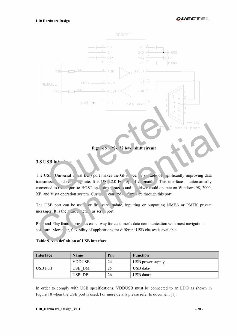
The UART port does not support the RS-232 level but only supports the LVTTL level. If the module’s
UART port is connected to the UART port of a computer, it is necessary to insert a level shift circuit
between the DCE and the computer. Please refer to the following figure.
Quectel
Confidential
L10 Hardware Design
L10_Hardware_Design_V1.1 - 20 -
Figure 9: RS-232 level shift circuit
3.8 USB interface
The USB (Universal Serial Bus) port makes the GPS receiver capable of significantly improving data
transmission and receiving rate. It is USB 2.0 Full-Speed compatible. This interface is automatically
converted to COM port to HOST operating systems and its driver could operate on Windows 98, 2000,
XP, and Vista operation system. Customer can update firmware through this port.
The USB port can be used for firmware update, inputting or outputting NMEA or PMTK private
messages. It is the same function as serial port.
Plug-and-Play feature provides easier way for customer’s data communication with most navigation
software. Moreover, flexibility of applications for different USB classes is available.
Table 9: Pin definition of USB interface
In order to comply with USB specifications, VDDUSB must be connected to an LDO as shown in
Figure 10 when the USB port is used. For more details please refer to document [1].
Interface Name Pin Function
USB Port
VDDUSB 24 USB power supply
USB_DM 25 USB data-
USB_DP 26 USB data+
Quectel
Confidential

L10 Hardware Design
L10_Hardware_Design_V1.1 - 21 -
USB Device connector
VBUS
DP
DM
GND
MODULE
VDDBUS
USBDP
USBDM
GND
LDO
5V 3.3V
Figure 10: USB interface circuit
Note: The USB interface is not recommended to output NMEA message to USB port of the host, such
as ARM processor because the driver of USB may be not reliable. If don't use the USB port, please
connect VDDUSB to GND.
3.9 Software upgrade
The UART port and USB port can be used for firmware upgrade, and one of them should be selected.
3.10 EXTINT0
The EXTINT0 pin is an external interrupt input pin. It is an edge trigger interrupt and can be used to
wake up the module from the standby mode. When the EXTINT0 pin is changed from high to low, the
module will enter the standby mode. When the EXTINT0 pin is changed from low to high, the module
will exit from standby mode.
Table 10: Pin definition of the EXTINT0
3.11 AOK
AOK can output antenna status message. It outputs a low level when the active GPS antenna is
assembled and operating normally. When the GPS antenna is not assembled or short-circuited, it outputs
a high level to indicate to the host controller.
Table 11: Pin definition of the AOK
Name Pin Function
EXTINT0 27 External interrupt input
Name Pin Function
AOK 12 Active GPS antenna status indication
Quectel
Confidential

L10 Hardware Design
L10_Hardware_Design_V1.1 - 22 -
3.12 I2C interface
The module has a standard I2C interface, but its driver is not embedded in the default firmware.
Table 12: Pin definition of the I2C interface
Note: This interface function is not supported in the default firmware. If customer wants a special
firmware, please contact Quectel.
Name Pin Function
SDA2 1 I2C data
SCL2 2 I2C clock
Quectel
Confidential

L10 Hardware Design
L10_Hardware_Design_V1.1 - 23 -
4 Antenna interface and supervisor
The L10 module receives L1 band signal from GPS satellites at a nominal frequency of 1575.42MHz.
The RF signal is connected to the RF_IN pin. Customer should use a controlled impedance transmission
line of 50 Ohm to connect to RF_IN.
4.1 Antenna
The L10 module can be connected to passive or active antenna. In the default operation mode the
antenna supervisor is activated and enables the receiver to detect short-circuit at the antenna port by
checking the bias voltage level and can shut down the voltage bias immediately when short-circuit
happens. NMEA messages are provided to report the condition of the antenna supply. Open-circuit
detection can also be supported with an additional external circuit. The reference design of the external
circuit is shown in Figure 11.
Figure 11: External detect circuit for open-circuit of active antenna
Table 13: Pin definition of the AADET_N
Name Pin Function
AADET_N 20 Active antenna detect input
Quectel
Confidential

L10 Hardware Design
L10_Hardware_Design_V1.1 - 24 -
Table 14: AADET_N and active antenna
The specification of active antenna is listed as Table 15.
Table 15: Antenna specification for L10 module
4.2 Antenna supply
4.2.1 Passive antenna
Passive antenna doesn't require a DC bias voltage and can be connected to RF_IN pin directly. V_ANT
can be connected to GND. It is always beneficial to reserve a passive matching network between the
antenna and the RF_IN port of the module. Figure 12 is the reference design.
Figure 12: Reference design for passive antenna
Active antenna state AADET_N Description
Open-circuit High Active antenna disconnected
OK Low Active antenna connected
Antenna type Specification
Passive antenna Center frequency: 1575.42 MHz
Band Width: >20 MHz
Gain: >0 dBi
Polarization: RHCP or Linear
Active antenna Center frequency: 1575.42 MHz
Band Width: >5 MHz
Minimum gain: 15-20dB(compensate signal loss in RF cable)
Maximum noise figure: 1.5dB
Maximum gain: 50dB
Polarization: RHCP or Linear
Quectel
Confidential

L10 Hardware Design
L10_Hardware_Design_V1.1 - 25 -
4.2.2 Active antenna
Active antenna has an integrated low-noise amplifier which could be connected to RF_IN directly. If an
active antenna is connected to RF_IN, the integrated low-noise amplifier of the antenna needs to be
supplied with the correct voltage through pin V_ANT. Usually, the supply voltage is fed to the antenna
through the coaxial RF cable. An active antenna consumes current at 5~20mA. The inductor inside the
module can separate the RF signal from the V_ANT pin and routes the bias supply to the active antenna.
The block diagram of the supply part for active antenna is shown in Figure 13.
Figure 13: Active antenna biasing
If the active antenna is short-circuited, the module would turn off the power supply to the antenna
immediately. Afterwards, the antenna status will be detected every 60 seconds. When the short-circuit
problem is removed, it will recover the power supply to the active antenna.
If the VCC_RF voltage is suitable for powering the active antenna, pin VCC_RF could be directly
connected to pin V_ANT. A reference circuit is shown in Figure 14.
Figure 14: Active antenna with VCC_RF
If the VCC_RF voltage doesn’t meet the requirement for powering the active antenna, an external LDO
could be used. The output of the external LDO can be connected to pin V_ANT. A reference circuit is
shown in Figure 15.
Quectel
Confidential

L10 Hardware Design
L10_Hardware_Design_V1.1 - 26 -
Figure 15: Active antenna with external LDO
If an external power supply and an external inductor are used to power the active antenna, the
short-circuit detection function could still work, but it couldn’t cut off the external power supply. So
customer is not recommended to do in this way.
Quectel
Confidential
L10 Hardware Design
L10_Hardware_Design_V1.1 - 27 -
5 Electrical, reliability and radio characteristics
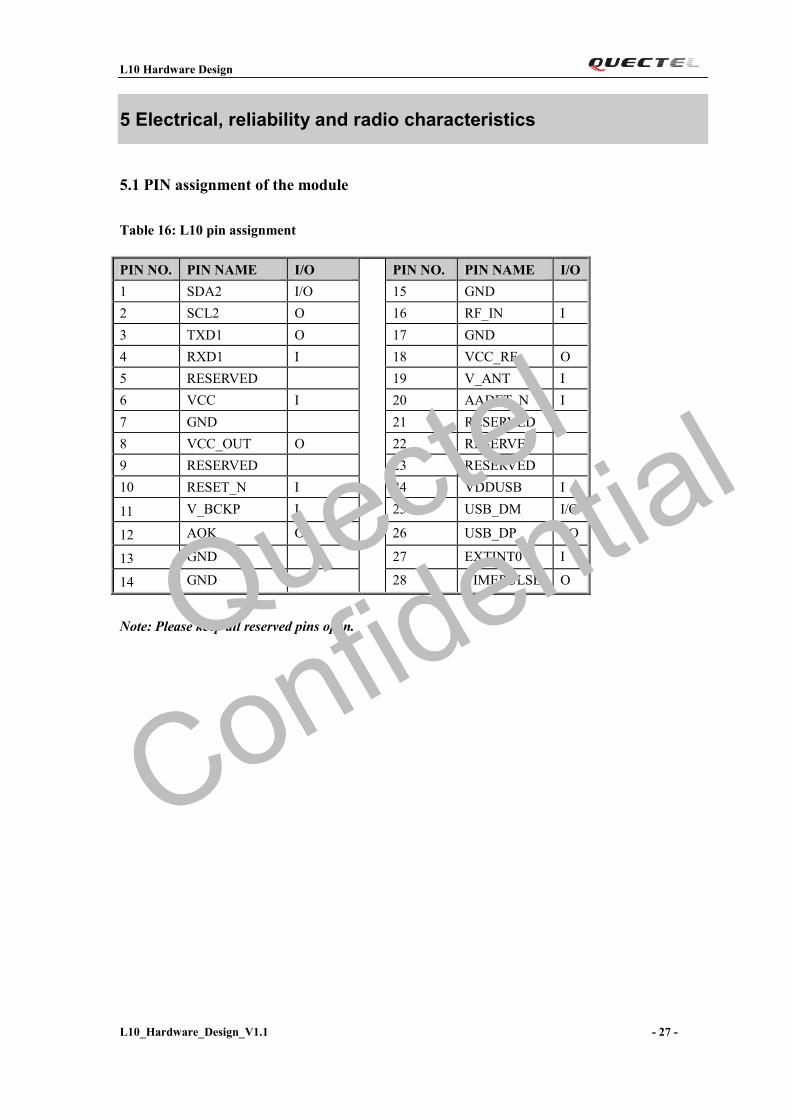
5.1 PIN assignment of the module
Table 16: L10 pin assignment
PIN NO. PIN NAME I/O PIN NO. PIN NAME I/O
1 SDA2 I/O 15 GND
2 SCL2 O 16 RF_IN I
3 TXD1 O 17 GND
4 RXD1 I 18 VCC_RF O
5 RESERVED 19 V_ANT I
6 VCC I 20 AADET_N I
7 GND 21 RESERVED
8 VCC_OUT O 22 RESERVED
9 RESERVED 23 RESERVED
10 RESET_N I 24 VDDUSB I
11 V_BCKP I 25 USB_DM I/O
12 AOK O 26 USB_DP I/O
13 GND 27 EXTINT0 I
14 GND 28 TIMEPULSE O
Note: Please keep all reserved pins open.Quectel
Confidential

L10 Hardware Design
L10_Hardware_Design_V1.1 - 28 -
5.2 Absolute maximum ratings
Absolute maximum rating for power supply and voltage on digital pins of module are listed in Table
17.
Table 17: Absolute maximum ratings
Parameter Min Max Unit
Power supply voltage (VCC) -0.3 4.3 V
Backup battery voltage (V_BCKP) -0.3 4.3 V
USB supply voltage (VDDUSB) -0.3 3.6 V
Input voltage at digital pins -0.5 3.6 V
-0.5 3.6 V
VCC_RF output current (Ivccrf) 50 mA
Input power at RF_IN (Prfin) 0 dBm
Antenna bias voltage(V_ANT) 0 6 V
Antenna bias current(Iant) 100 mA
Storage temperature -45 125 °C
Note: Stressing the device beyond the “Absolute Maximum Ratings” may cause permanent damage.
These are stress ratings only. The product is not protected against over voltage or reversed voltage.
If necessary, voltage spikes exceeding the power supply voltage specification, given in table above,
must be limited to values within the specified boundaries by using appropriate protection diodes.
5.3 Operating conditions
Table 18: The module power supply ratings
Parameter Description Conditions Min Typ Max Unit
VCC Supply voltage Voltage must stay
within the min/max
values, including
voltage drop, ripple,
and spikes.
3.0 3.3 4.3 V
IVCCP* Peak supply current VCC=3.3V 150 mA
V_BCKP Backup voltage
supply
2.0 3.3 4.3 V
IBCKP Backup battery
current
V_BCKP=3.3V 4 uA
V_ANT Antenna bias voltage 2.7 5.5 V
VANT_DROP Antenna bias 0.1 V
Quectel
Confidential

L10 Hardware Design
L10_Hardware_Design_V1.1 - 29 -
voltage drop
IANT V_ANT supply
current
V_ANT=3.3V 100 mA
VDDUSB USB supply voltage 3.0 3.3 3.6 V
VCC_RF Output voltage RF
section
VCC -0.1 V
IVCC_RF VCC_RF output
current
50 mA
TOPR Normal Operating
temperature
-40 25 85 ℃
* Use this figure to determine the maximum current capability of power supply.
Note: Operation beyond the "Operating Conditions" is not recommended and extended exposure
beyond the "Operating Conditions" may affect device reliability.
5.4 Current consumption
The values for current consumption are shown in Table 19.
Table 19: The module current consumption (passive antenna)
Note: In the standby mode, the power supply to active antenna through V_ANT is cut off. It will be
re-activated when the module exits from the standby mode.
5.5 Electro-static discharge
Although the module is fully protected against ESD strike, ESD protection precautions should still be
emphasized. Proper ESD handing and packaging procedures must be applied throughout the
processing, handing and operation of any application.
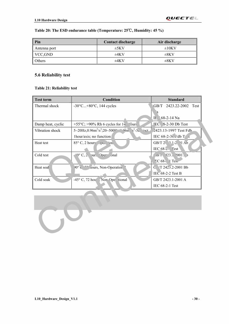
The ESD bearing capability of the module is listed in Table 20.
Parameter Condition Min Typ Max Unit
Icc Acquisition 43 mA
Icc Tracking
For Cold Start, 10 minutes after
First Fix. For Hot Start, 15 seconds
after First Fix.
38 mA
Icc Standby EXTINT0 pin is changed from
high to low. 2 mA
Quectel
Confidential
L10 Hardware Design
L10_Hardware_Design_V1.1 - 30 -
Table 20: The ESD endurance table (Temperature: 25℃, Humidity: 45 %)
Pin Contact discharge Air discharge
Antenna port ±5KV ±10KV
VCC,GND ±4KV ±8KV
Others ±4KV ±8KV
5.6 Reliability test
Table 21: Reliability test
Test term Condition Standard
Thermal shock -30°C...+80°C, 144 cycles GB/T 2423.22-2002 Test
Na
IEC 68-2-14 Na
Damp heat, cyclic +55°C; >90% Rh 6 cycles for 144 hours IEC 68-2-30 Db Test
Vibration shock 5~20Hz,0.96m2/s
3;20~500Hz,0.96m
2/s
3-3dB/oct,
1hour/axis; no function
2423.13-1997 Test Fdb
IEC 68-2-36 Fdb Test
Heat test 85° C, 2 hours, Operational GB/T 2423.1-2001 Ab
IEC 68-2-1 Test
Cold test -40° C, 2 hours, Operational GB/T 2423.1-2001 Ab
IEC 68-2-1 Test
Heat soak 90° C, 72 hours, Non-Operational GB/T 2423.2-2001 Bb
IEC 68-2-2 Test B
Cold soak -45° C, 72 hours, Non-Operational GB/T 2423.1-2001 A
IEC 68-2-1 Test
Quectel
Confidential

L10 Hardware Design
L10_Hardware_Design_V1.1 - 31 -
6 Mechanics
This chapter describes the mechanical dimensions of the module.
6.1 Mechanical dimensions of the module
Figure 16: L10 Top view and Side dimensions(Unit:mm)
Quectel
Confidential

L10 Hardware Design
L10_Hardware_Design_V1.1 - 32 -
Figure 17: L10 Bottom dimensions(Unit:mm)
Figure 18: PAD Bottom dimensions(Unit:mm)
Quectel
Confidential

L10 Hardware Design
L10_Hardware_Design_V1.1 - 33 -
6.2 Footprint of recommendation
Quectel
Confidential

L10 Hardware Design
L10_Hardware_Design_V1.1 - 34 -
Figure 19: Footprint of recommendation(Unit:mm)
Note1:Keep out on the host board below the module and the keep-out area should be covered by
solder mask and top silk layer for isolation between the top layer of host board and the bottom layer
of the module.
Note2:For easy maintenance of this module and accessing to these pads, please keep a distance no
less than 3mm between the module and other components in host board.
Quectel
Confidential

L10 Hardware Design
L10_Hardware_Design_V1.1 - 35 -
6.3 Top view of the module
Figure 20: Top view of the module
6.4 Bottom view of the module
Figure 21: Bottom view of the module
Quectel
Confidential

Shanghai Quectel Wireless Solutions Co., Ltd.
Room 501, Building 13, No.99 Tianzhou Road, Shanghai, China 200233
Tel: +86 21 5108 6236
Mail: [email protected]


