
Leveraging RRAM to Design Efficient
Digital Circuits and Systems for Beyond
Von Neumann in-Memory Computing
by
Zongxian Yang
A thesis
presented to the University of Waterloo
in fulfillment of the
thesis requirement for the degree of
Master of Applied Science
in
Electrical and Computer Engineering
Waterloo, Ontario, Canada, 2019
©Zongxian Yang 2019

ii
AUTHOR'S DECLARATION
I hereby declare that I am the sole author of this thesis. This is a true copy of the thesis, including any
required final revisions, as accepted by my examiners.
I understand that my thesis may be made electronically available to the public.

iii
Abstract
Due to the physical separation of their processing elements and storage units, contemporary digital
computers are confronted with the thorny memory-wall problem. The strategy of in-memory computing
has been considered as a promising solution to overcome the von Neumann bottleneck and design high-
performance, energy-efficient computing systems. Moreover, in the post Moore era, post-CMOS
technologies have received intense interests for possible future digital logic applications beyond the
CMOS scaling limits. Motivated by these perspectives from system level to device level, this thesis
proposes two effective processing-in-memory schemes to construct the non-von Neumann systems
based on nonvolatile resistive random-access memory (RRAM).
In the first scheme, we present functionally complete stateful logic gates based on a CMOS-compatible
2-transistor-2-RRAM (2T2R) structure. In this structure, the programmable logic functionality is
determined by the amplitude of operation voltages, rather than its circuit topology. A reconfigurable
3T2R chain with programmable interconnects is used to implement complex combinational logic
circuits. The design has a highly regular and symmetric circuit structure, making it easy for design,
integration, and fabrication, while the operations are flexible yet clean. Easily integrated as 3-
dimensional (3-D) stacked arrays, two proposed memory architectures not only serve as regular 3-D
memory arrays but also perform in-memory-computing within the same layer and between the stacked
layers. The second scheme leverages hybrid logic in the same hardware to design efficient digital
circuits and systems with low computational complexity. Multiple-bit ripple-carry adder (RCA),
pipelined RCA, and prefix tree adder are shown as example circuits, using the same regular chain
structure, to validate the design efficiency. The design principles, computational complexity, and
performance are discussed and compared to the CMOS technology and other state-of-the-art post-
CMOS implementations. The overall evaluation shows superior performance in speed and area. The
result of the study could build a technology cell library that can be potentially used as input to a
technology-mapping algorithm. The proposed hybrid-logic methodology presents prospect of hardware
acceleration and future beyond-von Neumann in-memory computing architectures.

iv
Acknowledgements
This dissertation would not have materialized without the guidance, encouragement, and help of
countless people who offered me their unfailing support. Without them, this work would not have been
achievable.
First and foremost, I would like to express my greatest gratitude to my supervisor, Prof. Lan Wei, who
has continuously given me precious guidance and support throughout my MASc study on both
coursework and research, for her patience, motivation, enthusiasm, and immense knowledge. At many
stages in the course of this research project I benefited from her advice, particularly so when exploring
new ideas. Our weekly meetings were always able to bring me findings, confidence, and direction. Her
careful editing contributed enormously to the production of our research papers and this thesis. I could
not have imagined having a better advisor and mentor for my research study.
I would like to thank the rest of my thesis committee: Prof. Hiren Patel, Prof. Peter Levine, for their
insightful comments and encouragement.
I owe great thanks to Prof. Manoj Sachdev and Prof. Hiren Patel for their suggestions and
encouragement from the early stages of important concepts from this research project.
I thank my fellow labmates in Waterloo Emerging Integrated System (WEIS) Group: Kaship Sheikh,
Hazem Elgabra, Yiju Zhao, Xuesong Chen, Shubham Ranjan, Rubaya Absar, Daniel Hui Zhou, and
Yixiao Ma, for the stimulating discussions, for the feedback during group meetings, and for all the fun
we had in the last two years.
Last but not the least, I would like to thank my family: my parents and my brothers, who have given
me all their love and encouragement, for supporting me spiritually throughout my life.

v
Dedication
I dedicate this to my mother Shunian Xie and father Ruifeng Yang.
vi
Table of Contents
AUTHOR'S DECLARATION ............................................................................................................... ii
Abstract ................................................................................................................................................. iii
Acknowledgements ............................................................................................................................... iv
Dedication .............................................................................................................................................. v
Table of Contents .................................................................................................................................. vi
List of Figures ..................................................................................................................................... viii
List of Tables ...................................................................................................................................... xiii
Chapter 1 Introduction ........................................................................................................................... 1
1.1 In-Memory Computing ................................................................................................................ 1
1.2 Resistive Random Access Memory (RRAM) .............................................................................. 3
1.3 Scope of Research ........................................................................................................................ 5
1.4 Organization ................................................................................................................................. 6
Chapter 2 Related Work ......................................................................................................................... 7
2.1 Digital R-R Stateful Logic ........................................................................................................... 7
2.2 Digital V-R Logic ........................................................................................................................ 9
2.3 Analog Computing using RRAM crossbar ................................................................................ 10
Chapter 3 Digital Design based on Stateful Logic ............................................................................... 12
3.1 Introduction ................................................................................................................................ 12
3.2 2T2R Stateful Logic Gate .......................................................................................................... 12
3.2.1 OP1: P’=P (bit hold) and Q’= P∙Q (AND) .......................................................................... 16
3.2.2 OP2: P’ = Q→P (Implication, IMP) and Q’=0 (bit set)................................................. 17
3.2.3 OP4: P’ = Q→P (Implication, IMP) and Q’= P∙Q (AND) .................................................. 17
3.3 3T2R Chain for Combinational Logic ....................................................................................... 20
3.3.1 XNOR Gate ......................................................................................................................... 21
3.3.2 1-bit Full Adder ................................................................................................................... 22
3.4 Design Evaluation and Comparison ........................................................................................... 24
3.5 Conslusions ................................................................................................................................ 27
Chapter 4 3-D Stacked Memory Arrays for Data Storage/PIM ........................................................... 28
4.1 Introduction ................................................................................................................................ 28

vii
4.2 3-D Memory Array 1 (mem1) .................................................................................................... 29
4.2.1 Conventional Random-Access Memory (RAM) Operations .............................................. 30
4.2.2 Processing-in-Memory (PIM) ............................................................................................. 31
4.3 3-D Memory Array 2 (mem2) .................................................................................................... 33
4.4 Conclusions ................................................................................................................................ 35
Chapter 5 Digital Design based on Hybrid Logic ................................................................................ 37
5.1 Introduction ................................................................................................................................ 37
5.2 2T2R Hybrid Logic Gate ............................................................................................................ 38
5.2.1 Logic Family 1 (LF1) .......................................................................................................... 41
5.2.2 Logic Family 2 (LF2) .......................................................................................................... 43
5.2.3 Logic Family 3 (LF3) .......................................................................................................... 45
5.3 Arithmetic Logic Block Design .................................................................................................. 48
5.3.1 1-bit Full Adder (FA) .......................................................................................................... 48
5.3.2 4-bit Ripple Carry Adder (RCA) ......................................................................................... 50
5.3.3 4-bit Pipelined Ripple Carry Adder (RCA) ......................................................................... 54
5.3.4 4-bit Prefix Brent-Kung Adder ............................................................................................ 56
5.4 Design Evaluation and Comparison ........................................................................................... 57
5.5 Readout Structure ....................................................................................................................... 60
5.6 Conclusions ................................................................................................................................ 61
Chapter 6 Conclusions and Future Work ............................................................................................. 62
6.1 Conclusions ................................................................................................................................ 62
6.2 Future Work ............................................................................................................................... 63
Bibliography ......................................................................................................................................... 64

viii
List of Figures
Figure 1.1 Processor-memory performance gap grows at a rate of 50%/year.
[https://cs.nyu.edu/courses/fall12/CSCI-GA.3033-012/lecture3.pdf] .................................................... 1
Figure 1.2 (a) Von Neumann structure and (b) beyond von Neumann structure based on in-memory
computing. ............................................................................................................................................. 2
Figure 1.3 (a) Schematic of metal-insulator-metal structure for oxide-RRAM and basic current-
voltage characteristics of (b) a unipolar RRAM and (c) a bipolar RRAM. [22] .................................... 3
Figure 1.4 RRAM working principle. (A) Formed and dissolved conductive filament resulting from
set and reset operations respectively in Metal/Insulator/Metal (MIM) structure. [Compact Modeling
Solutions for Oxide-Based Resistive Switching Memories (OxRAM)] (B) A filament growth model
for RRAM switching. The application of a positive voltage to the TE results in the migration of
positively ionized defects from the reservoir on the TE side (a) toward the BE, thus resulting in the
nucleation of the CF (b) and its growth at an increasing time (c), (d). The increase of the diameter of
the CF thus results in the decreasing resistance observed during the set transition. [45] ...................... 4
Figure 2.1 Resistance-to-resistance stateful logic (R-R logic) gate and illustration of the IMP
operation for the four input values of p and q. (a) IMP is performed by two simultaneous voltage
pulses, VCOND and VSET, applied to switches P and Q, respectively, to execute conditional toggling
on switch Q depending on the state of switch P. (b) The truth table for the operation q’ = p IMP q.
[13] ......................................................................................................................................................... 7
Figure 2.2 Schematic of (a) 2R stateful logic gate and (b) 2T2R structure used for experimental
verification. Two switches are connected in series, while the logic operation is dictated by the applied
voltage. [27] ........................................................................................................................................... 8
Figure 2.3 Voltage-to-resistance logic (V-R logic) gate and corresponding truth table for material
implication (IMP) operation. The V–R logic gate consists of a single resistive switch, where the input
signals are the applied voltages at the two ends of the device (X1 and X2) and the output signal is the
switch conductance state (Y). [11] ......................................................................................................... 9
Figure 2.4 Voltage-to-current logic, V-I logic. (a) Using a bitline to perform an analog sum of
products operation. (b) A memristor crossbar used as a vector-matrix multiplier. [34] ...................... 10
Figure 2.5 Pattern classification experiment (physical-level description). (a) An implementation of a
single-layer perceptron using a 10x6 fragment of the RRAM crossbar. (b) An example of the

ix
classification operation for a specific input pattern (stylized letter ‘z’), with the crossbar input signals
equal to +VR or -VR, depending on the pixel colour. (c) An example of the weight adjustment in a
specific (first positive) column, for a specific error matrix. [49]……………………………………..11
Figure 3.1 Current-voltage characteristics of the RRAM device used in this chapter. The device is
simulated with ASU RRAM model [23] calibrated to IMEC device [38]. (Inset shows an RRAM
device with two terminals (p as anode and n as cathode). .................................................................... 13
Figure 3.2 Proposed 2T2R logic gate with back-to-back RRAM pair. NMOS are simulated using
PTM65nm [39] at 500nm widths. An overdrive gate voltage is applied to transistors to reduce
transistor resistance and avoid any threshold voltage drop between gate and source. ......................... 14
Figure 3.3 Equivalent circuit transformation of the 2T2R logic gate. (a) A positive VUL applied to the
top terminal with Q/P as upper/lower cells is equivalent to (b) a negative VUL to the top terminal with
P/Q as upper/lower cells. It is also equivalent to (c) a positive VUL applied to the bottom terminal with
P/Q as upper/lower cells. All the operation voltages VUL are supposed to have the same amplitude
|VUL| to achieve the same computation result. ...................................................................................... 19
Figure 3.4 3T2R chain structure to implement complex combinational logic. (a) A two-unit 3T2R
chain example, the dashed box refers to one 3T2R unit. Reconfigurable interconnects to connect two
cells (highlighted in red): (b) one in the upper row and the other one in the lower row (P1 and P4); (c)
both in the upper row (P1 and P2). (d) The two-unit 3T2R chain is used to realize an XNOR gate, as
an example circuit (the dashed pass gate in the second 3T2R unit is in fact not needed in XNOR gate).
.............................................................................................................................................................. 20
Figure 3.5 Computation steps and control/operation signals to perform XNOR gate. The simulation is
performed as design verification when A=0, B=1. The XNOR gate needs four steps (10 ns for each
step) to compute/store the result A⊙B=0 in P4, highlighted in green. In each step, the input operands,
gate control/operation signals, operations, and computation results are listed in the table. Important
intermediate signals are annotated in the waveforms. .......................................................................... 22
Figure 3.6 A five-unit 3T2R chain to implement the 1-bit full adder. The dashed part in the chain is
not necessary in the adder implementation........................................................................................... 23
Figure 3.7 Computation steps to realize a 1-bit full adder. The simulation is performed as design
verification when A=1, B=0, and Cin=1. The adder circuit needs nine steps (10 ns for each step) to
compute/store Cout=1 in P10 and ten steps to obtain S=0 in P4, both highlighted in green. In each step,
the input operands, computation cells, operations, and intermediate results are annotated in the
waveforms accordingly. ....................................................................................................................... 24

x
Figure 3.8 Area comparison with CMOS designs for the 1-bit full adder. The 3T2R chain saves
~53% area from static adder, ~45% area from mirror adder and TG-based adder. ............................. 25
Figure 3.9 Design comparison with other state-of-the-art RRAM-based designs for the 1-bit full
adder. .................................................................................................................................................... 26
Figure 4.1 Mem1: (a) 3D crossbar array (mem1) based on the proposed 2T2R gates, (b) planform
schematic of the center physical stack (#5) containing upper cell 5U and lower cell 5L, and (c) bias
schemes for UL1 computation (WLs are not present for clarity). The transistors here could be
potentially replaced with selector devices to achieve the BEOL 3D stacking crossbars. .................... 28
Figure 4.2 Schematic of the layout (3-D view) for one stack in the memory array (mem1). Select line
(SL) connects the cathode of left RRAM (of lower cells) and the drain of right NMOS (of upper
cells). .................................................................................................................................................... 30
Figure 4.3 Bias schemes for 3-D memory array mem1 for different modes of in-memory
computation: . (a) UL2, (b) UU1, and (c) UU2. (d) Status of selected, half-selected (type I-III),
unselected cells/pairs during proposed CIM process. .......................................................................... 31
Figure 4.4 Simulation results for mem1: (a) UL1, (b) UL2, (c) UU1, (d) UU2 computation modes to
validate the corresponding bias schemes. Selected cells/pair undergo OP1 (bit hold and AND), while
half-selected type I, type II, and type III (with θ=0.5) remain undisturbed. ........................................ 33
Figure 4.5 Sneak path problem when conducting concurrent computations in mem1. ...................... 34
Figure 4.6 Mem2: (a) 3D crossbar array (mem2) by rearranging the mutual connections and
directions of the SL/BL in the mem1, (b) planform schematic of the center physical stack (#5)
containing upper cell 5U and lower cell 5L, and (c) bias schemes for UL1 computation (WLs are not
present for clarity). ............................................................................................................................... 35
Figure 1.7 Schematic of the layout (3-D view) for one stack in the memory array (mem2)………… 36
Figure 4.8 Bias schemes for 3-D memory array mem2 for different modes of concurrent in-memory
computations: (a) UL1, (b) UL2, (c) LL1, and (d) LL2. ......................................................................... 36
Figure 5.1 Current-voltage transfer characteristics of the RRAM device used in this chapter. The
device is simulated using ASU RRAM model [23] calibrated to IMEC’s HfOx-based RRAM device
[38]. Insets show the symbol of a bipolar RRAM device and SET/RESET voltage pulses. ............... 38
Figure 5.2 Proposed 2T2R hybrid logic (R/V-R logic) gate with two RRAMs connected back-to-
back. 2The four terminal voltages (VU, VL, GP, GQ) and two RRAM initial states before computation

xi
(P, Q) are encoded as six input operands. The two RRAM states after one-step computation (P’, Q’)
refer to two nonvolatile output results of the logic gate. ...................................................................... 39
Figure 5.3 Equivalent circuit transformation of the 2T2R hybrid logic gate. (a) The original logic gate
with Q/P as upper/lower cells is equivalent to (b) swapping VU and VL with P/Q as upper/lower cells
(swapping P and Q, GP and GQ). .......................................................................................................... 40
Figure 5.4 Full adder implementation with 2x 2T2Rs in three steps. The four RRAM-state transitions
after each step and the corresponding operation voltages are labeled. Step 1 is to calculate 𝐴 ⊕ 𝐶𝑖 and
𝐶𝑜. Step two is to input 𝐵. Step three is to obtain 𝑆. ............................................................................ 49
Figure 5.5 Schematic of a 4-bit RCA with repeated structure (2T2R chain). Each unit shown in the
dashed box is a 1-bit FA as the universal unit block. ........................................................................... 50
Figure 5.6 Schematic of the optimized design of 4-bit RCA. The more compact design saves about
half of the area, with greater customization. ........................................................................................ 51
Figure 5.7 (a) Computation flow chart of the 4-bit RCA. (b) The corresponding RRAM state
transition in each step. The values in the boxes represent the RRAM states at the corresponding
positions. For example, in the initialization step, the four RRAMs of least significant bit (LSB) FA
unit are programmed to (0, 1, A0, 0). Each bit FA is initialized in a uniform pattern as (0, 1, Ai, 0).
The missed boxes mean that there is no transition/operation in that step. ........................................... 52
Figure 5.8 (a) The RRAM state transition of the compact 4-bit RCA. The similar steps between
computing 𝐶2 and computing 𝐴3⊕ 𝐶3 and 𝐶4 are omitted for simplicity. (b) Simulation of
𝐴3𝐴2𝐴1𝐴0(0101) + 𝐵3𝐵2𝐵1𝐵0(1001) = 𝐶4𝑆3 𝑆2 𝑆1 𝑆0(01110) as a case study to verify the
design correctness (all the transistors are at minimum 60nm widths using TSMC 65nm library). The
simulations are performed in Cadence Spectre. Two electric voltage levels are required for the RCA
operations including VLF3=VGQ=3.5V and VGP = 3V. .......................................................................... 53
Figure 5.9 Schematic of the pipelined design of 4-bit RCA with two pipelining stages. The pipelining
requires another CCU2 as additional cost/area overhead to achieve parallel computation. ................. 54
Figure 5.10 Simulation of two sets of 4-bit add computations 𝐴3𝐴2𝐴1𝐴0(0101) +
𝐵3𝐵2𝐵1𝐵0(1001) = 𝐶4𝑆3 𝑆2 𝑆1 𝑆0(01110). The pipelining requires four more steps as additional
delay/latency overhead. ........................................................................................................................ 55
Figure 5.11 PG diagram of a 4-bit prefix Brent-Kung adder and its PG notations. The calculation of
C4/G3:0 is the critical path in this tree adder whose formula is shown as the equation. ........................ 56
Figure 5.12 (a) PG calculation implemented in one step on a 2T2R hybrid logic gate. (b) Circuit
schematic (five 2T2R gates connected by four PG NMOS transistors) of 4-bit Brent-Kung adder. (c)

xii
Simulation results of critical path calculation when performing 𝐴3𝐴2𝐴1𝐴0(0101) +
𝐵3𝐵2𝐵1𝐵0(1001) = 𝐶4𝑆3 𝑆2 𝑆1 𝑆0(01110). ................................................................................. 57
Figure 5.13 Area comparison of this work with CMOS designs for a 32-bit adder. The RCA of this
work saves ~75% area from mirror adder and TG-based adder, while the compact RCA saves ~87%
area. ...................................................................................................................................................... 58
Figure 5.14 Design comparison of this work w.r.t. delay (number of steps) and area (number of
RRAMs) with other state-of-the-art RRAM-based designs for a 32-bit adder. ................................... 59
Figure 5.15 Readout structure of the 3T2R chain. During read process, all PG transistors are ON and
a Vread is applied on the middle nodes. Other NMOS transistors in each 1T1R control the read-cell
selection (read enable control)………………………………………………………………………...60

xiii
List of Tables
Table 3-1 RRAM model parameters .................................................................................................... 13
Table 3-2 Ranges of voltages across the 2T2R pair to perform different operations (OP1-OP5) for
different k (=VSET/|V|RESET|) values. ...................................................................................................... 15
Table 3-3 Truth table for OP1: P’=P (bit hold), Q’=P·Q (AND) ........................................................ 16
Table 3-4 Truth table for OP2: P’=Q→P (IMP), Q’=0 (bit set) .......................................................... 17
Table 3-5 Truth table for OP4: P’=Q→P (IMP), Q’=P·Q (AND) ....................................................... 18
Table 3-6 Device technology used for design evaluation .................................................................... 25
Table 5-1 Truth table for P/Q and P’/Q’ when (VU, VL, GP, GQ) = (1, 0, 1, 1): P’=P (bit hold),
Q’=P·Q (AND). Q’=P·1 (bit transfer) operation is highlighted in green. ............................................ 41
Table 5-2 Variable assignments for 14 Boolean logics of output P’ in LF1 for one/two input operands
….……………………………………………………………………………………………………..42
Table 5-3 Variable assignments for 14 Boolean logics of output P’ in LF1 for multiple input operands
….……………………………………………………………………………………………………..42
Table 5-4 Truth table for P/Q and P’/Q’ when (VU, VL, GP, GQ) = (1, 0, 1, 1): P’=Q→P (IMP), Q’
=0 (bit set). P’=Q→0 (NOT) operation is highlighted in blue. ......................................................... 43
Table 5-5 Variable assignments for 16 Boolean logics of output P’ in LF2 for one/two input operands
.............................................................................................................................................................. 44
Table 5-6 Variable assignments for common logics of output P’ in LF2 for multiple input operands 45
Table 5-7 Truth table for P/Q and P’/Q’ when (VU, VL, GP, GQ) = (1, 0, 1, 1): P’=Q→P (IMP), Q’
=P·Q (AND). Q’=P·1 (bit transfer) operation is highlighted in green; P’=Q→0 (NOT)
operation is highlighted in blue……………………………………………………………………….46
Table 5-8 Variable assignments for common logics of output P’ in LF3 for one/two input
operands………………………………………………………………………………………….……46
Table 5-9 Variable assignments for common logics of output P’ in LF3 for multiple input
operands…............................................................................................................................................ 47
Table 5-10 Device technology used for design evaluation .................................................................. 58


1
Chapter 1
Introduction
1.1 In-Memory Computing
The ever-increasing artificial intelligent (AI) applications, including image recognition, speech
understanding, robot intelligence, and data analytics, demand high-performance computation and
memory resources. To fuel the development of these applications, hardware-friendly algorithms [1],
domain specific architecture [2] as well as post-CMOS emerging technologies [3] are under extensive
exploration. Researchers and engineers are attempting to address the challenges of hardware
acceleration from many aspects in order to design novel, efficient digital systems [4-5]. Examples are
solving the computing challenges [6], dealing with the memory challenges [7], and designing novel
architectures with emerging technologies [8]. In particular, in today’s big-data era, memory accesses
and data transfer between the central processing unit (CPU) and memory storage via the bus consume
the majority of the processing time and power [9]. The performance gap between the microprocessor
and computer memory (DRAM) keeps growing [10] at a rate of 50% per year as shown in Figure 1.1,
indicating that most of the single core performance loss is on the memory system due to the much
slower memory operations relative to those of the CPU. This is known as the von Neumann bottleneck,
which severely hinders the rapid development of high-performance and energy-efficient computing.
Figure 1.1 Processor-memory performance gap grows at a rate of 50%/year.
[https://cs.nyu.edu/courses/fall12/CSCI-GA.3033-012/lecture3.pdf]

2
Therefore, in-memory computing (IMC), also known as processing-in-memory (PIM), serves as a
promising method to address the “memory wall” challenges for future computer systems [11].
Attracting most attention among several paradigms from industry and academia, IMC paves a direct
and efficient way to design beyond von Neumann architectures (Figure 1.2), aiming to subvert the von
Neumann architecture by conducting computation tasks within the memory, exactly where the
computation operands are located [12]. This solution is efficient because it provides a clear method to
suppress the overhead in latency and power consumption to overcome the bottleneck. Among the
explorations in PIM scheme thus far, designs based on computational memory devices [13-16] are one
of the most effective implementations as efficient in-memory computing generally requires fast, low-
power, high-density, scalable devices. It benefits from the in-situ calculations of the nonvolatile
memory devices, which are capable of storing data and computing at the same time.
Figure 1.2 (a) Von Neumann structure and (b) beyond von Neumann structure based
on in-memory computing.
(a) (b)
CPU
ALU(Busy)
Control
Memory
Unutilized large internalbandwidth & parallelism
Multiple cyclesFetch largeoperand data
von Neumann structure
CPU
ALU(Idle)
Control
Compute in Memory
In place, atomic, ultra-longvector ops. in a single cycle
Only transfercontrol signal
Beyond von Neumann

3
1.2 Resistive Random Access Memory (RRAM)
Over the past few decades, progress in the semiconductor industry was enabled by the downscaling of
the metal-oxide-semiconductor field-effect transistor (MOSFET), serving as the workhorse of digital
complementary metal-oxide-semiconductor (CMOS) systems for modern chips. Today, however, this
scaling has reached a plateau due to several critical factors such as ever-increasing power dissipation
and heating issues (including the leakage currents), quantum mechanical effects, and intrinsic parameter
fluctuations [17]. To tackle this barrier, emerging devices such as carbon nanotube FETs (CNFETs)
[18], resistive random access memories (RRAMs) [19], and superconducting devices [20] are
investigated to support post-CMOS technologies [21].
Resistive switching devices, such as RRAM, have widespread use among these post-CMOS
memories. RRAM is a new RAM technology to watch out for, while RAM is an important part of all
computing systems as it helps improve process and read-write speeds. This means that applications
running on a computer or laptop are able to perform much better and faster. It employs resistive-
switching characteristics in a simple sandwiched metal-insulator-metal structure to store binary
information using its resistance in a nonvolatile manner [22]. As shown in inset of Figure 1.3(a), a
bipolar RRAM device consists of two terminals, a top electrode (TE, anode p) and a bottom electrode
(BE, cathode n) and a metal-oxide layer in between. Its resistive switching is typically induced by
application of a voltage on the two electrodes (Vpn), which leads to the formation and rupture of a
conductive filament (CF) in the insulator layer driven by the electrical field along the x direction, shown
Figure 1.3 (a) Schematic of metal-insulator-metal structure for oxide-RRAM and basic current-
voltage characteristics of (b) a unipolar RRAM and (c) a bipolar RRAM. [22]

4
in Figure. 1.4. In a bipolar RRAM, a positive voltage beyond a threshold value (VSET), i.e. when
Vpn>VSET>0, forms CF to short the two electrodes, thus changing the RRAM state from a high resistance
state (HRS) to a low resistance state (LRS). On the contrary, a negative voltage below a certain negative
threshold (VRESET), i.e. when Vpn<VRESET<0, causes rupture of CF, switching its state from LRS back to
HRS. The two transition processes are named SET and RESET, respectively. Overall, RRAM possesses
advantages of simple device structure, high density, low power, fast speed, descent scalability, and
(A)
(B)
Figure 1.4 RRAM working principle. (A) Formed and dissolved conductive filament resulting
from set and reset operations respectively in Metal/Insulator/Metal (MIM) structure.
[Compact Modeling Solutions for Oxide-Based Resistive Switching Memories (OxRAM)] (B)
A filament growth model for RRAM switching. The application of a positive voltage to the
TE results in the migration of positively ionized defects from the reservoir on the TE side (a)
toward the BE, thus resulting in the nucleation of the CF (b) and its growth at an increasing
time (c), (d). The increase of the diameter of the CF thus results in the decreasing resistance
observed during the set transition. [45]

5
excellent compatibility with the CMOS process [22], [23]. Therefore, this computation memory has
been considered as a suitable candidate not only for next-generation high-density storage but also in
emerging circuit design and novel computation systems [24-26]. In addition, the use of RRAM (R)
could help to address power dissipation in emerging processors by employing transistor (T) or selector
(S) device as switch to form the 1T1R or 1S1R structure.
1.3 Scope of Research
In this thesis, we propose two PIM schemes in the digital domain based on 2-transistor-2-RRAM
structure, where the two bipolar RRAMs are connected in a back-to-back manner. In the first scheme,
we start from introducing the logic gate principle and then design a unified circuit structure to perform
any combinational logic. The computation methodologies are discussed accordingly. In addition, two
possible 3-D stacked memory array structures (mem1 and mem2) capable of both regular memory
functions and CIM, are illustrated to support large-scale integration. The stacked memory arrays can
perform the computation flexibly (within one same layer or between different stacking layers), enabled
by multiple computation modes. The second memory array, mem2, is able to carry out concurrent
computations, enhancing the processing parallelism and efficiency.
In the second scheme, we propose a hybrid-logic computation methodology in the same circuit, 2-
transistor-2-RRAM (2T2R) structure, which fully utilizes available computation resources. The hybrid
logic encodes input variables as both voltage levels and RRAM states, while the output results are
stored and represented by the RRAM states after operation. The hybrid-logic gate is still nonvolatile as
it is capable of storing computation results. For this scheme, we illustrate the hybrid-logic design
principle and show multiple logic families (LFs) of the 2T2R available to be used in arithmetic circuits.
Boolean logics for multiple operands (up to six) can be implemented efficiently in a single operational
step. Following that, the 1-bit full adder is realized with low complexity, in three steps with only two
cascaded 2T2R gates. Multiple-bit ripple-carry adder (RCA), pipelined RCA with higher throughput,
and logarithmic (tree) Brent-Kung adder with full parallelism are shown to build larger digital systems,
all using a repeated and regular chain structure. The designs are discussed and evaluated based on their
computational complexity. Eventually, the work is compared to commercial 65nm CMOS technology
and some popular RRAM-based computing platforms with regard to their speed and area. The overall
result of the evaluation shows superior performance and prospect in the future beyond-von Neumann
IMC architectures.

6
1.4 Organization
This thesis is divided up into four main sections. In Chapter 2, an overview of related work based on
the emerging technologies as well as their advantages and disadvantages are presented to the readers.
Chapter 3 illustrates the design of (1) functionally complete, stateful logic gates based on 2T2R; (2) a
regular, repeated, and reconfigurable 3T2R chain with programmable interconnects. Chapter 4 presents
the design of two dense 3-D stacked memory array structures, the second one capable of performing
concurrent computations. The 3-D arrays integrate the functionalities of processing element and storage
together, with multiple computation modes available to achieve flexible calculations inside the
memory. Lastly, in Chapter 5, we propose another efficient in-memory computing scheme based on
hybrid logic in 2T2R RRAM whose programmable logic functionality is determined by the amplitude
of voltage operands and variable assignments. A repeated, uniform, and reconfigurable 2T2R-gate
chain with programmable interconnects is designed to efficiently implement any arithmetic logic block.

7
Chapter 2
Related Work
In-memory computing schemes have been explored in both digital and analog spaces. In the last 20
years, the major digital IMC based on computational memories has been focusing on defining novel
logic gate concepts to carry out digital Boolean operations with lower energy and area consumption
[27-31]. Some works such as [13], [27], [29] deal with general implementations containing the basic
operations like bitwise OR, AND, XOR, and INV. The analog IMC takes advantages of dense RRAM
crossbar to implement the acceleration of matrix-vector multiplication, which has been extensively used
in AI applications such as machine learning algorithms.
2.1 Digital R-R Stateful Logic
An early work [13], back to 2010, experimentally demonstrates the material implication (IMP,
commonly used among logicians) in a relatively simple RRAM-based circuit combining a conventional
resistor to enable stateful logic operations (belongs to the family of resistance-to-resistance stateful
logic, R-R logic, shown in Figure 2.1). The IMP is a fundamental but powerful Boolean logic operation
Figure 2.1 Resistance-to-resistance stateful logic (R-R logic) gate and illustration of
the IMP operation for the four input values of p and q. (a) IMP is performed by two
simultaneous voltage pulses, VCOND and VSET, applied to switches P and Q,
respectively, to execute conditional toggling on switch Q depending on the state of
switch P. (b) The truth table for the operation q’ = p IMP q. The detailed operation
principle can be found in [13].

8
on two operands (p and q) such that “p IMP q” is equivalent to “(NOT p) OR q”. Containing an
inversion function (NOT), it is able to form a computationally complete logic basis through the
iterations of IMP logic. However, the IMP itself is only able to execute computations with lengthy
iterative operations, increasing the difficulty to implement certain logics flexibly (e.g. EQUAL) and
build large digital systems efficiently. In addition, the circuit needs extra resistors to assist each IMP
operation so that they add great area overhead and reduce program margin.
In [27], the stateful nonvolatile RRAM logic (whose input and output operands are both RRAM
states) is designed for normally-off digital computing by adopting a serial resistive switch arrangement
(shown in Figure 2.2). The switching devices (or switches) both store the input/output states, and
operate in response to an applied driving pulse. Different logic functions are achieved by different
values of the pulse voltage, e.g., high/low voltages, or positive/negative voltages. AND, IMP, NOT,
and bit transfer operations are demonstrated, each using a single clock pulse, while other functions (e.g.,
OR and XOR) are achieved in multiple steps.
The R-R nonvolatile logic approach allows suppressing the static leakage power dissipation while
reducing the area consumption because of the scalable two-terminal structure of the RRAM switch.
RRAM stateful logic differs from CMOS logic by the topological organization of the logic gate; in
CMOS logic, each logic function has a specific circuit topology. R-R stateful logic instead totally lacks
topological organization of the logic gates, thus allowing for standardization of the circuit architecture
through the adoption of the crossbar array with extremely high density. Nevertheless, a third resistance
Figure 2.2 Schematic of (a) 2R stateful logic gate and (b) 2T2R structure used for
experimental verification. Two switches are connected in series, while the logic
operation is dictated by the applied voltage. [27]

9
state needs to be programed into RRAM devices by adjusting the compliance current. Moreover, the
logic circuits require expensive and complicated reconfigurable wiring which add area overhead. In
each step, the cell connections have to be changed, which is hard to achieve in practical applications.
2.2 Digital V-R Logic
Instead of R-R mapping method, the work in [32] uses the two voltage values applied to the two
terminals of an RRAM device (has to be initially prepared in a low resistance state) as the two input
variables. The output of the logic gate is stored as the final state of the device (belongs to the family of
voltage-to-resistance logic, V-R logic). The relationship between the input voltages and output
resistance is also an IMP function, magically. Although the single IMP logic is far from designing high-
performance digital systems, the two works above brought the previously uncommon digital logic IMP
into many RRAM-based designs, which is internally intrinsic in the operations of resistive memories.
In the V–R logic gate, the output result remains stored as the resistive state without any voltage bias,
thus allowing a considerable saving of static power. On the other hand, the efficient sequential cascade
of two operations is impossible, as input and output signals are physically different. Converting the
output resistance into an input voltage can be achieved by additional circuits, typically located out of
the memory area.
Figure 2.3 Voltage-to-resistance logic (V-R logic) gate and corresponding truth table
for material implication (IMP) operation. The V–R logic gate consists of a single
resistive switch, where the input signals are the applied voltages at the two ends of
the device (X1 and X2) and the output signal is the switch conductance state (Y). [11]

10
2.3 Analog Computing using RRAM crossbar
From the viewpoint of in-memory computing, the crossbar array naturally provides a hardware
accelerator for analogue, approximated matrix–vector multiplication (MVM). Therefore, dense RRAM
crossbars are widely utilized to accelerate MVM of neural networks, leveraging the property of natural
current accumulation (KCL) to realize the addition function [33]. This popular method attributes to the
family of voltage-to-current logic, V-I logic, in which RRAM resistance stores parameters (pre-trained
network weights) rather than input or output operand information. The work in [34] explores an in-situ
processing approach, where memristor crossbar arrays not only store input weights, but are also used
to perform dot-product operations in an analog manner. The analog MVM in the crosspoint can be
carried out in one step, as opposed to the digital MAC operation, which is a time and energy-consuming
step in classical computers.
Another important work [49] reports the experimental demonstration of a fully operational neural
network based on an integrated, transistor-free crossbar with metal-oxide RRAM with device
variability sufficiently low to allow operation of integrated neural networks, in a simple network: a
single-layer perceptron (an algorithm for linear classification). This crossbar performed, on the physical
(Ohm’s law) level, the analogue vector-by-matrix multiplication, which is by far the most
computationally intensive part of the operation of any neuromorphic network used repeatedly in the
Figure 2.4 Voltage-to-current logic, V-I logic. (a) Using a bitline to perform an analog sum
of products operation. (b) A memristor crossbar used as a vector-matrix multiplier. [34]
(a) Multiply-Accumulate operation (b) Vector-Matrix Multiplier

11
same environment. The network can be taught in situ using a coarse-grain variety of the delta rule
algorithm to perform the perfect classification of 3x3 3-pixel black/white images into three classes
(representing letters).
Additionally, some more works attempt to improve the design efficiency by employing new structures
and computation methods. Recent examples are 1T1R RRAM [31], [35], hybrid CMOS circuits [36],
memristor ratioed logic (MRL) [44], complementary resistive switches (CRS) crossbar [37]. These
works shift the digital design focus from gate level (basic bitwise operations) to arithmetic-block level
(adders and multipliers). Nevertheless, crucial problems such as the cascade, leakage current or
destructive-read still exist and thus severely restrict their strategies in practical application. Although
some of them are solvable, such as the cascade problem in [31], where the implementation supports
gate cascading in a complex manner, it needs an additional readout step for cascade using complicated
peripheral circuits such as sense amplifiers, block decoders, register stack, etc. As a consequence, this
thesis aims to propose a novel structure and computational methodologies to design digital logic circuits
and building blocks of arithmetic logic unit (ALU) by leveraging the capability and advantages of post-
CMOS RRAM in implementing beyond-von Neumann processing in-memory architectures.
Figure 2.5 Pattern classification experiment (physical-level description). (a) An
implementation of a single-layer perceptron using a 10x6 fragment of the RRAM crossbar.
(b) An example of the classification operation for a specific input pattern (stylized letter ‘z’),
with the crossbar input signals equal to +VR or -VR, depending on the pixel colour. (c) An
example of the weight adjustment in a specific (first positive) column, for a specific error
matrix. [49]

12
Chapter 3
Digital Design based on Stateful Logic
3.1 Introduction
In this chapter, we propose a stateful IMC scheme in the digital domain based on a symmetric 2-
transistor-2-RRAM structure, where the two bipolar RRAMs are connected in the back-to-back manner.
We start from introducing the logic gate principle and then design a unified circuit structure to perform
any combinational logic circuits. All the input and output operands are RRAM resistive states in this
stateful logic gate. The design has a highly regular and symmetric circuit structure, while the operations
are flexible yet clean (without the need of complicated peripheral circuitry or a third resistive state).
Implementations of XNOR and full-adder functions using 3T2R chain without extra routing/control
gates or resistors are shown as example circuits to demonstrate the arithmetic unit design. The proposed
computing scheme is intrinsic and efficient for PIM applications and presents superior performance in
speed and area. The computation methodologies, design principles, and advantages/disadvantages are
discussed in details accordingly.
3.2 2T2R Stateful Logic Gate
Figure 3.1 depicts the I-V characteristics of a bipolar HfOx-based RRAM device, generated by ASU
RRAM model [23] using HSPICE. The model used in this thesis is calibrated to match the experimental
HfOx-RRAM device behavior from IMEC [38] with 20mV/s SET/RESET pulses. In the HSPICE
simulation, faster pulses (0.2 V/ns) are used which result in VSET = 2V and VRESET = -1.33V. The relevant
parameters used in this RRAM model are listed in Table 3.1 (“g” parameters represent gap distance,
which is defined as the average distance between the TE and the tip of the CF).
The structure of the proposed 2T2R logic gates is shown in Figure 3.2, where the two serial bipolar
RRAMs are connected in a back-to-back manner. The two NMOS transistors act as access devices to
each RRAM. The operation is explained as follows. First, prepare two RRAM resistive states as two
inputs: P (initial state of lower cell) and Q (initial state of upper cell). The initialization can be done by
applying SET/RESET voltages between top/bottom terminal and the middle node “M” (labelled in
Figure 3.2). Then apply three voltage pulses simultaneously on the corresponding terminals: VUL
(operational voltage), GP (enable/control voltage of the lower cell), and GQ (enable/control voltage of

13
the upper cell). Finally, the two outputs of the logic gate are in situ stored as the RRAM states after the
operation: P’ (final state of lower cell) and Q’ (final state of upper cell). Overdrive gate voltages are
Parameter Value Parameter Value
( 𝐴)
I-V fitting parameter61.4 ( )
I-V fitting parameter0.275
( )
I-V fitting parameter0.43
Gap dynamics fitting parameter1
Gap dynamics fitting parameter1.25
Gap dynamics fitting parameter16.5
( )
Gap dynamics fitting parameter150 ( )
Activation energy for vacancy generation1.501
( )
Activation energy for vacancy recombination1.5 ( )
Oxide thickness5
( )
Effective thermal time constant0.23 ( )
Atomic hopping distance0.25
( )
Maximum gap distance1.367 ( )
Ambient temperature298
( )
Minimum gap distance0.543 𝐶 ( )
Effective thermal capacitance0.318
Figure 3.1 Current-voltage characteristics of the RRAM device used in this chapter.
The device is simulated with ASU RRAM model [23] calibrated to IMEC device [38].
(Inset shows an RRAM device with two terminals (p as anode and n as cathode).
Table 3-1 RRAM model parameters
14
applied to transistors to reduce transistor resistance and avoid any threshold voltage drop between gate
and source. The concept and operation are similar to those introduced in [13] and [27]. In this work,
the LRS (50kΩ) and HRS (1MΩ) represents logic “0” and logic “1”, respectively. However, this design
does not require additional resistors to assist logic operation as compared with [13]. Additionally, the
upper cell and lower cell are connected back-to-back (p-n-n-p) rather than the p-n-p-n connection in
[27]. Due to the back-to-back configuration in this logic gate, by applying a positive VUL, the upper cell
Q can only go through SET process (no RESET possible) while lower cell P can only go through
RESET process (no SET possible). The opposite case happens when VUL is negative. This proposed
2T2R structure offers several significant advantages:
1) Improved program margin as no voltage drops across the extra resistors.
2) No need of the third resistive state (a quasi-LRS, 0*, achieved by adjusting the compliance
current) to trigger the effective operation, as discussed in [27].
VGP=2.5V
VGQ=VOP1=3V
2 ns 8 ns0 10 ns
Voltages for OP1
Figure 3.2 Proposed 2T2R logic gate with back-to-back RRAM pair. NMOS are
simulated using PTM65nm [39] at 500nm widths. An overdrive gate voltage is applied
to transistors to reduce transistor resistance and avoid any threshold voltage drop
between gate and source.

15
3) Capability to form regular and symmetric chain structure to design combinational logic
circuit and 3D stacked memory array structure (for both RAM storage and CIM),
tremendously reducing the design complexity.
4) Elimination of additional routing control to reconfigure the interconnect between the
operation cells as in [27]. This feature is reflected in Section 4, where any two of the cells
from different stacks are already automatically connected in a back-to-back manner.
5) The logic function of the gate is determined by the amplitude of operation voltage (VUL)
instead of the circuit itself, possessing superior reconfigurability.
To explain the logic gate principles, first, we define a parameter k as
𝑘 = 𝑉𝑆𝐸𝑇
|𝑉𝑅𝐸𝑆𝐸𝑇| (3.1)
which is the ratio of SET and RESET voltage. For different RRAM devices with different k values, the
available operation combinations (OPs) and their corresponding VUL ranges are also different. All the
possible cases are listed in Table 3.2. However, for any given bipolar RRAM device, i.e. any given k,
the operations AND and IMP are always achievable, guaranteeing the functional completeness. In this
chapter, the operations are proved based on the IMEC’s device presented in Figure 3.1, whose k equals
to 1.5.
Given one specific RRAM with fixed k value, there are a few logic operations available, enabled by
different ranges of VUL (operation voltage across the RRAM pairs). For the RRAM used in this work
with k=1.5, three operations OP1, OP2, and OP4 will be analyzed in details in Chapter 3.2.1, 3.2.2, and
kVOP1 for OP1:bit hold (P’=P)AND (Q’= P∙Q)
VOP2 for OP2IMP (P’=Q→P)bit set (Q’=0)
VOP3 for OP3:bit hold (P’=P)bit set (Q’=0)
VOP4 for OP4:IMP (P’=Q→P)AND (Q’=P·Q)
VOP5 for OP5:IMP (P’=Q→P)bit hold (Q’=Q)
<1 (VSET, 2VSET) >2|VRESET| (2VSET, 2|VRESET|) N/A N/A
1 (VSET, 2VSET) >2VSET N/A N/A N/A
(1, 2) (VSET, 2|VRESET|) >2VSET N/A (2|VRESET|, 2VSET) N/A
2 N/A >2VSET N/A (VSET, 2VSET) N/A
>2 N/A >2VSET N/A (VSET, 2VSET) (2|VRESET|, VSET)
Table 3-2 Ranges of voltages across the 2T2R pair to perform different operations
(OP1-OP5) for different k (=VSET/|V|RESET|) values.

16
3.2.3, respectively. OP3 and OP5 under other k cases can be obtained similarly, as summarized in Table
I. All OPs in Table I are given with positive value of VUL.
3.2.1 OP1: P’=P (bit hold) and Q’= P∙Q (AND)
In OP1, the range of operation voltage, VUL, is given by
𝑈𝐿 = 𝑂𝑃 ∈ ( 𝑆𝐸𝑇 , 2| 𝑅𝐸𝑆𝐸𝑇|). (3.2)
In the cases of P=Q=0 or P=Q=1, VOP1 will be equally distributed on the upper and lower cells since
they have the same resistance (both in LRS or both in HRS). Hence, the voltages across the P and Q
have the following relationship
𝑄𝑝𝑛 = − 𝑃𝑝𝑛 = 0.5 𝑂𝑃 ∈ (0.5 𝑆𝐸𝑇 , | 𝑅𝐸𝑆𝐸𝑇|) < | 𝑅𝐸𝑆𝐸𝑇| (3.3)
where VQpn is less than VSET and |VPpn| is less than |VRESET|, neither sufficient to trigger any transitions.
When P=0 and Q=1, VOP1 is dropped mainly across Q (VQpn≈VOP1>VSET, VLpn≈0) due to much higher
resistance. Thus a SET process is initiated on the upper cell Q so that Q’=0 (LRS). Meanwhile, lower
cell P remains at LRS so that P’=0. In the case of P=1 and Q=0, almost all of VOP1 drops across P
(VQpn≈0, VPpn≈-VOP1). Since P is already in HRS, i.e. RESET state, no transition could take place, thus
P’=1 and Q’=0. The truth table containing all the input and output cases is summarized in Table 3.3 as
the result of above analysis. The table indicates the Boolean functions of the outputs, with regard to
inputs, are P’=P (bit hold) and Q’=P∙Q (AND). A special case can be used to perform “bit transfer”
operation, i.e. Q’=P, highlighted in green, if the initial state of upper cell is prepared in HRS (Q=1).
This allows the data stored in upper/lower cell to be transferred to lower/upper cell, important for the
gate cascade, chain logic and CIM array operations in Chapter 3.3 and Chapter 4.
P Q P’=P Q’=P·Q0 0 0 00 1 0 01 0 1 01 1 1 1
Table 3-3 Truth table for OP1: P’=P (bit hold), Q’=P·Q (AND)
Q’=P·1 (bit transfer) operation is highlighted in green
17
3.2.2 OP2: P’ = Q→P (Implication, IMP) and Q’=0 (bit set)
In OP2, the range of operation voltage, VUL, is given by
𝑈𝐿 = 𝑂𝑃2 > 2 𝑆𝐸𝑇 > 2| 𝑅𝐸𝑆𝐸𝑇|. (3.4)
In the case of P=Q=0, similarly, VOP2 will be averagely divided by the upper and lower cells. So the
voltages across the P and Q are
𝑄𝑝𝑛 = − 𝑃𝑝𝑛 = 0.5 𝑂𝑃2 > 𝑆𝐸𝑇 > | 𝑅𝐸𝑆𝐸𝑇| (3.5)
now the |VPpn| is greater than |VRESET|, which is sufficient to trigger a RESET transition on P so that P’
equals to 1 after operation. Similar analysis from OP1 applies for the cases of (P=1, Q=0) and (P=0,
Q=1). For P=Q=1, the voltage relationship is same as the one displayed in Eq. (5), where VQpn is greater
than VSET, also sufficient to initiate a SET transition on Q so that Q’ equals to 0 after operation. The
truth table as in Table 3.4 summarizes all the combinations. The Boolean functions available in OP2
are P’=Q→P (IMP) and Q’=0 (bit set). The material implication (IMP) function, proposed by [12], is
significant as it guarantees logic completeness, based on which any arbitrary Boolean function can be
transformed into the form of multiple IMPs. In addition, same as in OP1, a special case can be used to
perform a NOT function, i.e. P’=Q→0=NOT (Q), highlighted in blue, if the initial state of the lower
cell is prepared in LRS (P=0). The NOT operation of OP2 and the AND operation of OP1, from another
combinational point of view, offer functionally complete logic as well.
3.2.3 OP4: P’ = Q→P (Implication, IMP) and Q’= P∙Q (AND)
In OP4, the range of operation voltage, VUL, is given by
𝑈𝐿 = 𝑂𝑃 ∈ (2| 𝑅𝐸𝑆𝐸𝑇|, 2 𝑆𝐸𝑇). (3.6)
P Q P’=Q→P Q’=0
0 0 1 00 1 0 01 0 1 01 1 1 0
Table 3-4 Truth table for OP2: P’=Q→P (IMP), Q’=0 (bit set)
P’=Q→0 (NOT) operation is highlighted in blue

18
The outputs of (P=Q=0), (P=0, Q=1), and (P=1, Q=0) can be derived exactly same as the cases in OP2.
When P=Q=1, VOP2 will be equally divided between P and Q as they have same high resistance. As a
result, the voltages across the P and Q are
𝑄𝑝𝑛 = − 𝑃𝑝𝑛 = 0.5 𝑂𝑃4 ∈ (| 𝑅𝐸𝑆𝐸𝑇|, 𝑆𝐸𝑇) < 𝑆𝐸𝑇 (3.7)
where VQpn is less than VSET, not enough for implementing a SET process on Q anymore. Therefore,
the outputs stay at the same states as initial states.
For all of the above operation combinations, each of them is effectively completed in one-step
operation, only by applying the corresponding operational voltage VUL. However, the (0, 1) to (0, 0)
transition in Table 3-5 could be unstable due to the additional step/transition from (0, 0) to (1, 0) if the
pulses/voltages are not properly designed. In this section, the voltage pulses are predesigned and chosen
as inset shown in Figure 3.2 to avoid this over-operation, just like those in multilevel RRAMs. An
alternative approach is that we could add a current limiter (compliance) in the path to constrain the
current so that after (0, 1), (0, 0) would not change continuously to next (1, 0). It is also worth noting
that because both the input and output variables are RRAM states, the cascade of the 2T2R logic gates
could be easily achieved in two ways: (1) through a bit-transfer operation in OP1 or OP4, propagating
the output of the current gate to one of the inputs (prepared/initialized as “1”) of the next stage; (2)
through the pass gate transistor of the following 3T2R chain in Section 3.3 to select different RRAM
pairs in action. In addition, note that thick-oxide transistors might be required due to reliability
concerns (out of the scope of this thesis). Due to the symmetry of the 2T2R structure, application of a
negative VUL with same amplitude performs exactly same operations as its positive counterparts by
P Q P’=Q→P Q’=P·Q0 0 1 00 1 0 01 0 1 01 1 1 1
Table 3-5 Truth table for OP4: P’=Q→P (IMP), Q’=P·Q (AND)
Q’=P·1 (bit transfer) operation is highlighted in green
P’=Q→0 (NOT) operation is highlighted in blue

19
exchanging the positions of upper and lower cells, i.e. exchanging P/Q and P’/Q’ in the functions
resulted from |VUL| (as shown in Figure 3.3(a) and 3.3(b)). When negative VUL is applied on the top of
the structure, the two gate control voltages, VGQ and VGP, need to be calibrated accordingly.
Alternatively, we can just swap the relative positions of upper and lower cells and apply a positive VUL
on the bottom terminal to obtain the equivalent results (as shown is Figure 3.3(c)). The equivalent
circuit conversions are presented in Figure 3.3, providing flexibility in designing combinational circuits
and memory arrays in the following Sections. In this chapter, all transistors are implemented using the
Predictive Technology Model (PTM) [39] with the same size, W/L=500nm/65nm, simulated in
HSPICE. The voltage drops across these transistors are marginal at ON states. If narrower transistors
are used, the voltage drop across NMOS will have to be considered and compensated in VUL.
(a) (b) (c)
Figure 3.3 Equivalent circuit transformation of the 2T2R logic gate. (a) A positive
VUL applied to the top terminal with Q/P as upper/lower cells is equivalent to (b) a
negative VUL to the top terminal with P/Q as upper/lower cells. It is also equivalent
to (c) a positive VUL applied to the bottom terminal with P/Q as upper/lower cells.
All the operation voltages VUL are supposed to have the same amplitude |VUL| to
achieve the same computation result.

20
3.3 3T2R Chain for Combinational Logic
To implement more complex arithmetic functions based on the 2T2R logic gate, a 3T2R chain structure
is designed to connect multiple 2T2R units through one NMOS pass gate transistor (1T), as circled in
(a) (b)
(b) (d)
Figure 3.4 3T2R chain structure to implement complex combinational logic. (a) A
two-unit 3T2R chain example, the dashed box refers to one 3T2R unit.
Reconfigurable interconnects to connect two cells (highlighted in red): (b) one in
the upper row and the other one in the lower row (P1 and P4); (c) both in the upper
row (P1 and P2). (d) The two-unit 3T2R chain is used to realize an XNOR gate, as
an example circuit (the dashed pass gate in the second 3T2R unit is in fact not
needed in XNOR gate).

21
the dashed box of Figure 3.4(a). The back-to-back connection (p-n-n-p) of 2T2R makes it possible that
any two of the 1T1R cells in the chain can form a 2T2R pair to perform the OPs discussed in Chapter
3.2, regardless of the RRAMs positions. The node “In” is used to initialize states of RRAMs by applying
SET/RESET voltages between “In” and “Ti”. The reconfigurable/programmable interconnects are
realized by the gate control signals (1/0 for connection/disconnection) of these transistors (G1-Gx).
That is to say, logic gates can be inter-wired in different configurations, which is similar to the
architecture of a field-programmable-gate-array (FPGA). For example, the combination of (G1, G2,
G3, G4, Gx) = (1, 0, 0, 1, 1) enables the red path connecting two cells, P1 and P4, one in the upper row
and the other one in the lower row (Figure 3.4(b)). The path in Figure 3.4(c) is formed when (G1, G2,
G3, G4, Gx) = (1, 1, 0, 0, 1) in order to perform OPs on P1 and P2. The programmable interconnects
can be realized by leveraging static random access memories (SRAMs) for gate controls (G1, G2, G3,
G4, Gx), which is in-system programmable and re-programmable. The data stored in SRAM (0/1)
controls routing of the chain (open/short). The idea is similar to that of SRAM-based FPGAs to obtain
reconfigurable interconnects. The proposed 3T2R architecture eliminates the need to change or add
additional routing and controls to form the p-n-p-n pair as discussed in [27]. Additionally, more gates
are added in [16] to change the interconnects and configure cells in p-n-p-n sequence. These extra gates
are used differently for different logics, increasing both design complexity and area.
3.3.1 XNOR Gate
The two-unit 3T2R chain can implement an XNOR gate using IMP/AND functions (Equation 3.8),
𝐴⊙ 𝐵 = (𝐴 + ) ∙ ( + 𝐵) = (𝐵 → 𝐴) ∙ (𝐴 → 𝐵). (3.8)
as an example circuit, which is shown in Figure 3.4(d). The dashed transistor is not required for the
operation, reducing the area needed of the XNOR logic. Figure 3.5 depicts the four computation steps,
10 ns for each step, to perform an XNOR function when A=0 and B=1, corresponding to the method
of Eq. (8). The result A⊙B=0 is computed and in situ stored in the cell P4 in the 4th step. In the
simulation, the VUL are set to be VOP1 = 2.5V, VOP2 = 4.2V, and VOP4=3V for OP1, OP2, and OP4,
respectively. If narrower transistors and/or a longer chain are used, VOP or VG will have to be adjusted
to accommodate the voltage drop across the transistors.

22
3.3.2 1-bit Full Adder
Following the implementation of XNOR gate in the previous section, a 1-bit full adder is realized to
demonstrate the design of arithmetic block units. A 3T2R chain with five units can perform a 3-operand
(A, B, and Cin) addition as shown in Figure 3.6. The computation methodologies for carry out (Cout)
and Sum (S) are given by the following equations.
𝑆 = 𝐴⊕𝐵⊕ 𝐶 = 𝐴⊕𝐵⊕ 𝐶𝑖 → 0
= [(𝐶 → (𝐴⊕𝐵)) · ((𝐴 ⊕𝐵) → 𝐶 )] → 0; (3.9)
𝐶𝑜𝑢 = 𝐴𝐵 + 𝐵𝐶 + 𝐴𝐶 = 𝐴𝐵 → [(𝐴⊕ 𝐵) · 𝐶 ]
= 𝐴𝐵 → [(𝐴ʘ𝐵) → 0] · 𝐶 ]. (3.10)
Initial 1st Clock Cycle 2nd Clock Cycle 3rd Clock Cycle 4th Clock Cycle
Control/ OperationSignals
Enable G1-4Disable GxT3, T4: VOP1
T1, T2: ground
Enable G2, G3, GxDisable G1, G4
T2: VOP4
T3: groundT1, T4: float
Enable G1, G4, GxDisable G2, G3
T1: VOP4
T4: groundT2, T3: float
Enable G3, G4, GxDisable G1, G2
T4: VOP1
T3: groundT1, T2: float
P10=A P13 = P12·P42
P20=B P22 = P21·P31
P30=1 P31 = P10·P30 P32 = P21→P31 P34 = P33
P40=1 P41 = P20·P40 P43 = P12→P42 P44 = P33·P43
P1
P2
A
B
B → A
A → B
A = 0
B = 1
A ʘ B=0
1M
200k40k
1M
200k40k
1M
200k40k
1M
200k40k
P3
P4
Res
ista
nce
[Ω
]
0 10 20 30 40
Time [ns]
Figure 3.5 Computation steps and control/operation signals to perform XNOR gate. The
simulation is performed as design verification when A=0, B=1. The XNOR gate needs four steps
(10 ns for each step) to compute/store the result A⊙B=0 in P4, highlighted in green. In each
step, the input operands, gate control/operation signals, operations, and computation results
are listed in the table. Important intermediate signals are annotated in the waveforms.

23
As plotted in Figure 3.7, the adder unit needs nine steps to calculate Cout and ten steps for S, guided by
the computing procedures of XNOR and Equations (3.9), (3.10). The implementation is verified by
simulation to compute the results when A=1, B=0, and Cin=1. The intermediate result A⊙B=0 is
obtained in the 4th step and duplicated in 5th step (through bit transfer operation) to be reused because
both Cout and S need it for their individual calculations. The results Cout=1 is stored in P10 in 9th step
and S=0 is finally in situ computed in P4.
Figure 3.6 A five-unit 3T2R chain to implement the 1-bit full adder. The dashed
part in the chain is not necessary in the adder implementation.

24
3.4 Design Evaluation and Comparison
AB
AʘB
AʘB
A⊕B
(A⊕B)→
(A⊕B) =
=
P1
P2
P3
P4
P6
P7
P8
P9
P10
A=1
B=0
=1
P10·P60
P20·P70
P40·P90
P21→P61
P21·P61
P12→P72
P12·P72
P63·P73
P74·P84
P85→P105
P85·P105
P106→P96
P96·P106
P37·P97
P27→P17
P76→P36
P36·P76
P18→P108
P18·P108
P99→P49
P49·P99
P42→P32
P32·P42
A
B
HRS
LRS
HRS
LRS
HRS
LRS
HRS
LRS
HRS
LRS
HRS
LRS
HRS
LRS
HRS
LRS
HRS
LRS
0 10 20 30 40 50 60 70 80 90 100
Time [ns]
Res
ista
nce
[Ω
]Clock cycle 1 2 3 4 5 6 7 8 9 10
Figure 3.7 Computation steps to realize a 1-bit full adder. The simulation is
performed as design verification when A=1, B=0, and Cin=1. The adder circuit needs
nine steps (10 ns for each step) to compute/store Cout=1 in P10 and ten steps to obtain
S=0 in P4, both highlighted in green. In each step, the input operands, computation
cells, operations, and intermediate results are annotated in the waveforms
accordingly.

25
Validated by the realization of example circuits, XNOR and 1-bit full adder, the 3T2R chain
architecture is capable of implementing any combinational circuits. Theoretically, it is able to solve any
problem statefully which is computable. The proposed 3T2R chain greatly simplifies the design and
fabrication of the complex digital combinational circuits. The functionality of the unified/repeated
chain is only determined by the external control and operation signals, independent of the circuit
structure. The design focuses on finite state machines (FSMs) to generate and control the data path to
be employed by the predesigned/prefabricated circuits, whose principle differs from the modern
application-specific integrated circuits (ASIC) designs. This feature indicates that the chain block can
be reprogrammed to implement different logic functions, just like a FPGA, allowing flexible
Device Technology
RRAM − e t e si e ( ) 5
𝐴 − A e ( 2) 100 (4 2)
CMOS − ( ) 65
𝐴 − ( 2) 8450 (2 2)
0
50000
100000
150000
200000
250000
Static Mirror TG This work
Are
a [
nm
2]
Area comparison for
32-bit Adder design
53%45%
Table 3-6 Device technology used for design evaluation
Figure 3.8 Area comparison with CMOS designs for the 1-bit full adder. The
3T2R chain saves ~53% area from static adder, ~45% area from mirror adder
and TG-based adder.

26
reconfigurable computing as performed in computer software. Meanwhile, the logic circuits are
normally-off thanks to the fact that the computation results and intermediate information are all stored
in the nonvolatile RRAM devices, dispelling the concern of interrupted power supply during compute
process.
The performance of a computing scheme is evaluated by its computational complexity, i.e. spatial
complexity and temporal complexity. As for RRAM-based logic circuits in this work, the required
number of RRAMs and transistors represents spatial complexity; temporal complexity is the
computation steps/cycles it takes. First, the 3T2R chain design is compared to 65 nm CMOS technology
based on a 1-bit full adder implementation. The device technology used for evaluation is listed in Table
3.6. Compared to CMOS static adder, mirror adder, and transmission-gate (TG) based implementations,
this 3T2R chain saves around 53%, 45%, and 45% area, respectively.
Furthermore, the 1-bit full adder design of 3T2R chain is compared to other popular state-of-the-art
RRAM-based implementations [13], [29], [31], [37], [40], [41], with respect to their delay (steps) and
area (RRAMs). Overall, the 3T2R chain demonstrates superior performance. Siemon’s [37] adder is
based on implication logic using CRS cells which requires complicated peripheral circuitry to assist the
operations. Not only that, the CRS itself has a “destructive read” problem, restricting the application.
0 50 100 150 200 250
Lehtonen
Kvatinsky
Siemon (CRS)
Snider
Xie
Wang (1T1R)
This work
Number
State-of-the-art RRAM-based 32-bit Adders
Delay (step)
Area (RRAM)
[40]
[29]
[37]
[13]
[41]
[31]
Figure 3.9 Design comparison with other state-of-the-art RRAM-based designs for
the 1-bit full adder.

27
Wang’s [31] 1T1R RRAM implementation is efficient as it encodes inputs as both voltages and RRAM
states. However, the disadvantage is also obvious as the sophisticated peripheral circuits including
sense amplifiers, block decoders, and register stack are mandatory to support the in-memory operation.
This is mainly due to the requirement of state-to-voltage conversion. On the contrary, for this work, the
structure is regular and simple with clean operations [42].
3.5 Conslusions
Processing-in-memory provides an effective means to conquer the restrictions of existing von
Neumann-based computing methodologies. It is able to subvert the conventional computer’s
architecture and eliminate the memory wall of modern digital systems. This chapter proposes a
promising scheme for such applications, from gate level to circuit level, finally to system-architecture
level. It illustrates the design of (1) functionally complete, stateful logic gates based on 2T2R; (2) a
regular, repeated, and reconfigurable 3T2R chain with programmable interconnects. The design is
comprehensively evaluated and compared with contemporary CMOS digital designs and other
emerging schemes based on post-CMOS technologies as well, from the perspectives of design
principle, circuit structure, difficulty of integration and fabrication, and performance. The study in this
chapter is possible to push forward and accelerate the development of emerging computing and novel
architectures in the post-Moore microelectronics industry.

28
Chapter 4
3-D Stacked Memory Arrays for Data
Storage/PIM
4.1 Introduction
In this chapter, two possible 3-D stacked memory array structures (mem1 and mem2) capable of both
regular memory functions and CIM, are illustrated to support large-scale integration. The stacked
memory arrays can perform the computation flexibly (within one same layer or between different
stacking layers), enabled by multiple computation modes. The regular RAM operations and CIM
(a)
Figure 4.1 Mem1: (a) 3D crossbar array (mem1) based on the proposed 2T2R gates, (b)
planform schematic of the center physical stack (#5) containing upper cell 5U and lower cell
5L, and (c) bias schemes for UL1 computation (WLs are not present for clarity). The
transistors here could be potentially replaced with selector devices to achieve the BEOL 3D
stacking crossbars.

29
schemes are discussed. In addition, possible layout structure and sneak path problem are also
mentioned. The status of half-selected and unselected cells when performing in-memory operations on
the selected cells are presented, bias schemes proposed to protect undesired ones from disturbance. The
second memory array, mem2, is able to carry out concurrent computations by rearranging/redefining
the WL/SL/BL directions, enhancing the processing parallelism and efficiency via off NMOS or
lowering the voltages across them. The mem2 has strong potential to be adopted as practical 3-D dense
memory storage and in the future PIM applications where the computations require substantial parallel
processing.
4.2 3-D Memory Array 1 (mem1)
Following the implementations of digital logic circuits, we propose a 3-D array (mem1) based on the
proposed 2T2R gates so as to achieve dense in-memory operations for large scale integration. The
memory array has multiple stacked layers, two of them schematically shown in Figure 4.1(a). The upper
layer contains upper cells (1T1Rs) with same polarity direction while the lower layer is built by lower
cells with reverse polarities. Two 1T1Rs of adjacent layers or of same layer could form a basic 2T2R
gate to perform previously introduced OPs. For this 3-D array, two sets of bitlines (BLs) run in the
horizontal direction: BLU as the top nodes of the upper cells and BLL to the bottom nodes of the lower
cells. Two sets of wordlines (WLs), WLU and WLL, run in the vertical direction as switch controls of
upper and lower 1T1R cells, respectively. Another set of select lines (SLs) run in parallel with WLs,
connecting the middle nodes of each 2T2R stack sharing same WLs. Figure 4.1(b) displays a 2-D stick
figure to describe the vertical view of one physical stack, the stack #5 in the center of the 3x3 array,
with control signals. The planform of the 3x3 3-D array is pictured in Figure 4.1(c), WLs are omitted
for clarity. Figure 4.2 briefly depicts the 3-D view of the physical implementation for one stack in the
memory array (mem1). Further area saving and structure simplification could be achieved by replacing
the NOMS transistors with simpler selector devices, which is able to result in practical CMOS-
compatible back-end of line (BEOL) 3-D stacking crossbars.

30
4.2.1 Conventional Random-Access Memory (RAM) Operations
The 3-D array described above can be used as a conventional RRAM-based RAM. To write/read a
particular cell (e.g. 5U in the array in Figure 4.1(c)), the operations are similar to those of 1T1R arrays:
WLUB is set high (enabled) while all other WLU and all WLL are set low (disabled). All SL are grounded.
BLUB are set to VSET, VRESET, and Vread (=2V, -1.33V, and 0.1V in this chapter, respectively) for SET,
RESET, and read operations, respectively. Other BLU and BLL all are grounded.
BLL
GateInsulator
Source Drain Source Drain
BLU
WLUWLL
InsulatorGate
Substrate
RRAMRRAM
SiO2
SL
n
n
p
p
interconnect
Figure 4.2 Schematic of the layout (3-D view) for one stack in the memory array
(mem1). Select line (SL) connects the cathode of left RRAM (of lower cells) and the
drain of right NMOS (of upper cells).

31
4.2.2 Processing-in-Memory (PIM)
The proposed 2T2R-gate OPs can be mapped and performed in this 3-D array, interactions taking place
in different adjacent layers or within the same layer. There are basically four computation modes
available. First, we explain how to compute a pair formed by two cells from different layers, an upper
cell and a lower cell, at the same physical stack. Figure 4.1(c) gives an instance of 5U-5L pair (stack
#5) in the 3x3 array to illustrate the first mode “UL1”. WLUB and WLLB are set to high to select two
cells 5U and 5L, while all the other WLs are grounded (disabled). All SLs are floating to allow free
operation on middle nodes. For the selected cells (5U and 5L), BLUB is biased at various VUL to trigger
different OPs, V0 =VOP1 for OP1 or V0=VOP2 for OP2, etc. As for BLs, BLLB is grounded to establish a
path from BLUB and all other BLU and BLL are floating. Under this bias scheme, there exists four types
(d)
Cell/pair type Max voltage across NMOS+RRAM
NMOS ON?
Unselected 0 (BL/SL floating) No
Half-selectedtype I
V0 No
Half-selected type II
0 (BL/SL floating) Yes
Half-selected type III
(1- θ)V0 o θV0Yes
Selected V0 Yes
Figure 4.3 Bias schemes for 3-D memory array mem1 for different modes of in-memory
computation: . (a) UL2, (b) UU1, and (c) UU2. (d) Status of selected, half-selected (type I-III),
unselected cells/pairs during proposed CIM process.

32
of cells here defined by the bias/control conditions (painted in different colors): (1) selected cells/pair
(5U, 5L); (2) half-selected cells type I (4U, 4L, 6U, 6L), sharing biased BL with the selected cells; (3)
half-selected cells type II (2U, 2L, 8U, 8L), sharing WL and SL with the selected cells; (4) unselected
cells (others). The selected pair will go through designated computation according to amplitude of V0.
During this process, all other cells preserve their states since no unwanted voltage can impose on the
RRAMs. More specifically, RRAMs in half-selected type I cells are disconnected from V0 (biased BL)
due to disabled (OFF) NMOS (Figure 4.1(a)). As for half-selected type II cells which are connected
with selected cells through SLB, their NOMS are ON. Nevertheless, since the BLs of them are floating,
voltages of BLs will just follow SLB. Consequently, there is zero voltage drop across these cells, not
affecting their states.
Other three modes are defined by how the selected pair is composed: (1) “UL2” mode (Figure 4.3(a)):
an upper cell and a lower cell from different layers (5U and 8L), at different stack sharing the same SL;
(2) “UU1”/“LL1” mode (Figure 4.3(b)): an upper/lower cell with another upper/lower cell of the same
layer (2U/2L and 5U/5L), sharing the same SL; (3) “UU2”/“LL2” mode (Figure 4.3(c)): an upper/lower
cell with another upper/lower cell of the same layer (5U/5L and 6U/6L), sharing the same BL. Note in
UU2/LL2 computation mode, another half-selected type III cells (2U, 3U, 8U, 9U) share both SL and
WL with selected cells (5U and 6U). For these third-type cells, operation disturbance (state transition)
is supposed to be avoided on them by biasing the BL of these cells at a separate voltage θV0 to ensure
that the voltage drop across them are lower than the minimum voltage of VSET and |VRESET|. The bias
scheme is labelled as in Figure 4.3(c). Constant θ needs to be restricted by the following range so as to
not trigger any SET/RESET process.
1 − 𝑆𝐸𝑇 , | 𝑅𝐸𝑆𝐸𝑇| < θ < 𝑆𝐸𝑇 , | 𝑅𝐸𝑆𝐸𝑇| (4.1)
The table shown in Figure 4.3(d) summarizes the status including cell bias and transistor status of
the all the types of cells/pairs. Furthermore, to validate the bias schemes, simulation is carried out to
verify that none of the half-selected cells and unselected cells are disturbed during OP1 computation
(bit transfer and AND) on the selected cells/pair (shown in Figure 4.4).

33
Taking the advantage of various and flexible computation modes proposed above, complicated PIM
schemes are achievable. We propose two schemes as case studies here.
1) Use both upper and lower layers identically, for storage and computation.
2) Use one layer (e.g. upper layer) as regular RAM only for the general purpose of memory
storage and another layer (lower layer) for the processing process (feasible within the same
layer as discussed previously). One can transfer the data stored in the upper layer cells to
lower layer when necessary (via bit transfer operation of OP1/OP4 under UL1/UL2 modes).
Then, the fetched data can be processed using lower layer cells (via all available logic gates
under LL1 and/or LL2).
More sophisticated combinations and processing algorithms can be explored to manage data storage
and sequential computation steps. We could even attempt to integrate 3T2R chain for logic circuits and
3-D memory array together to realize more efficient PIM.
4.3 3-D Memory Array 2 (mem2)
Although the mem1 leverages the 2T2G logic gate and is good at performing flexible in-memory
operations, it is still hard for it to enhance the processing efficiency by carrying out concurrent
computations (compute multiple 2T2R pairs at the same time) owing to “sneak path” problem. When
the transistors are turned on for multiple cells, current will also flow on paths from other rows through
5U = 1 5U' = 0
5L = 0 5L' = 0
2U = 1 2U' = 1
2L = 0 2L' = 0
4U = 1 4U' = 1
4L = 0 4L' = 0
5U' = 5U·5LHRS
LRS
HRS
LRS
HRS
LRS
HRS
LRS
HRS
LRS
HRS
LRS
5U = 1 5U' = 0
8L = 0 8L' = 0
8U = 1 8U' = 1
5L = 0 5L' = 0
4U = 1 4U' = 1
7L = 0 7L' = 0
5U' = 5U·8L5U = 1 5U' = 0
2U = 0 2U' = 0
8U = 1 8U' = 1
4U = 1 4U' = 1
1U = 0 1U' = 0
5U' = 5U·2U6U = 1 6U' = 0
5U = 0 5U' = 0
3U = 1 3U' = 1
2U = 0 2U' = 0
6U' = 5U·6UR
esis
tan
ce [
Ω]
0 10
Time [ns]
0 10
Time [ns]
0 10
Time [ns]
0 10
Time [ns]
(a) (b) (c) (d)
3L = 1 3L' = 1
2L = 0 2L' = 0
Figure 4.4 Simulation results for mem1: (a) UL1, (b) UL2, (c) UU1, (d) UU2 computation modes
to validate the corresponding bias schemes. Selected cells/pair undergo OP1 (bit hold and
AND), while half-selected type I, type II, and type III (with θ=0.5) remain undisturbed.

34
select line (similar to the sneak-path problem in conventional RRAM crossbar array). Voltage will be
divided from the middle point between RRAM cells and may affect the transition state. The extra paths
could cause computation errors. This is schematically described by Figure 4.5.
In order to facilitate concurrency, the second 3-D stacked memory array configuration (mem2) is
designed by simply rearranging the mutual connections and directions of the SL/BL in the mem1. The
structure of mem2 is pictured in Figure 4.6(a). The parallel computations are supported by mem2 for
modes: UL1, UL2, LL1, LL2 (followed by similar mode definition of mem1). The 3-D view of the
physical implementation for one stack of mem2 is presented in Figure 4.7. The single pair computation
under UL1 is shown in Figure 4.6(c), while the parallel computations under UL1 computes selected
pair #2, #5, and #8 concurrently (Figure 4.8(a)). All other cells remain unselected due to OFF NMOS.
Furthermore, concurrent computations under modes UL2, LL1, and LL2 with parallelism are drawn as
in Figure 4.8. The simulation is done to validate the correctness of parallelism for mem2. Note that
there is no UU1 and UU2 modes available in mem2, meaning that the interaction within the upper layer
is not achievable in this array due to shared connections of upper cells. However, it excellently offers
Figure 4.5 Sneak path problem when conducting concurrent computations in mem1.
35
us computation concurrencies under other modes so that we can process data more efficiently for
applications like matrix manipulations, ubiquitous in machine learning.
4.4 Conclusions
This chapter discusses two dense 3-D stacked memory array structures, the second one capable of
performing concurrent computations. The 3-D arrays integrate the functionalities of processing element
and storage together, with multiple computation modes available to achieve flexible calculations inside
the memory.
(b)
(c)
(a)
Figure 4.6 Mem2: (a) 3D crossbar array (mem2) by rearranging the mutual connections and
directions of the SL/BL in the mem1, (b) planform schematic of the center physical stack
(#5) containing upper cell 5U and lower cell 5L, and (c) bias schemes for UL1 computation
(WLs are not present for clarity).

36
(a) (b)
(c) (d)
Figure 4.8 Bias schemes for 3-D memory array mem2 for different modes of concurrent
in-memory computations: (a) UL1, (b) UL2, (c) LL1, and (d) LL2.
SLL
GateInsulator
Source Drain Source Drain
SLU
WLUWLL
InsulatorGate
Substrate
RRAMRRAM
SiO2
BL
n
n
p
p
Figure 4.7 Schematic of the layout (3-D view) for one stack in the memory array (mem2).
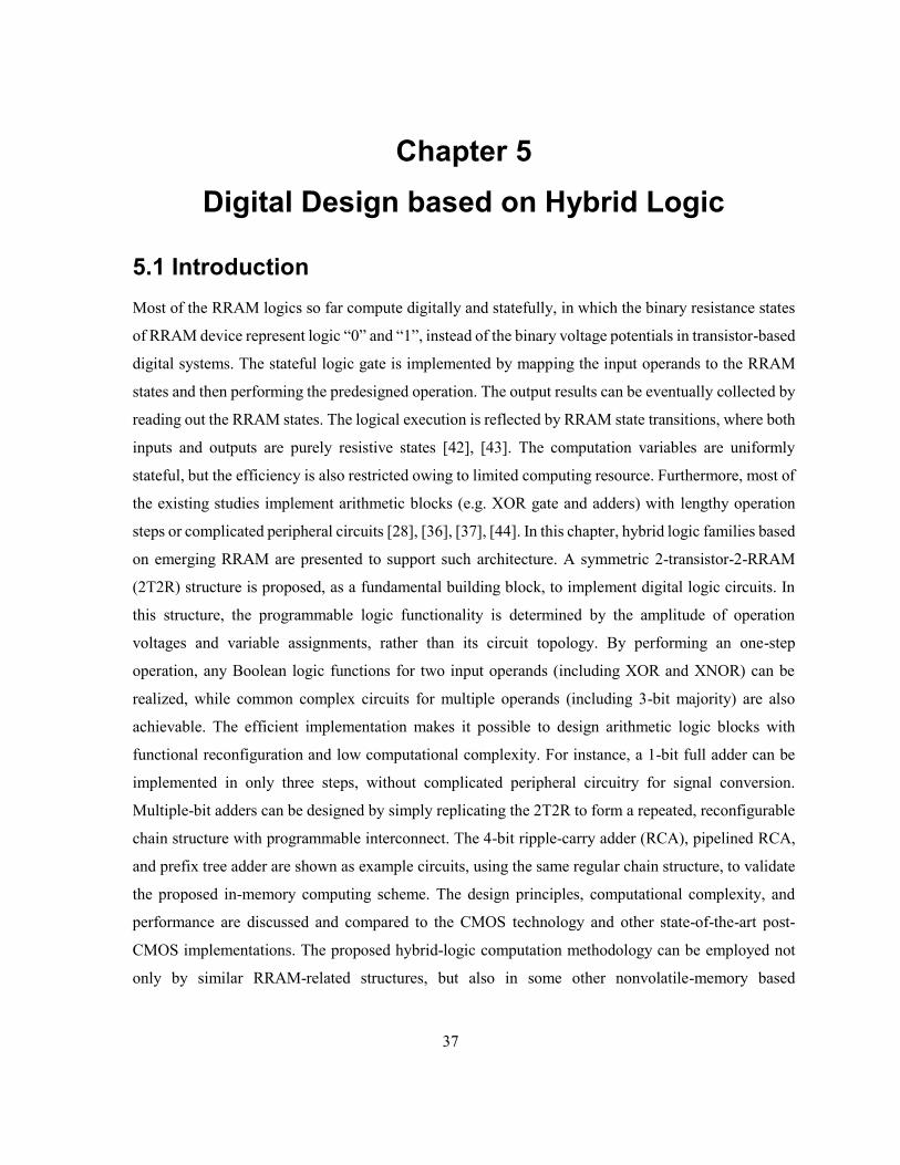
37
Chapter 5
Digital Design based on Hybrid Logic
5.1 Introduction
Most of the RRAM logics so far compute digitally and statefully, in which the binary resistance states
of RRAM device represent logic “0” and “1”, instead of the binary voltage potentials in transistor-based
digital systems. The stateful logic gate is implemented by mapping the input operands to the RRAM
states and then performing the predesigned operation. The output results can be eventually collected by
reading out the RRAM states. The logical execution is reflected by RRAM state transitions, where both
inputs and outputs are purely resistive states [42], [43]. The computation variables are uniformly
stateful, but the efficiency is also restricted owing to limited computing resource. Furthermore, most of
the existing studies implement arithmetic blocks (e.g. XOR gate and adders) with lengthy operation
steps or complicated peripheral circuits [28], [36], [37], [44]. In this chapter, hybrid logic families based
on emerging RRAM are presented to support such architecture. A symmetric 2-transistor-2-RRAM
(2T2R) structure is proposed, as a fundamental building block, to implement digital logic circuits. In
this structure, the programmable logic functionality is determined by the amplitude of operation
voltages and variable assignments, rather than its circuit topology. By performing an one-step
operation, any Boolean logic functions for two input operands (including XOR and XNOR) can be
realized, while common complex circuits for multiple operands (including 3-bit majority) are also
achievable. The efficient implementation makes it possible to design arithmetic logic blocks with
functional reconfiguration and low computational complexity. For instance, a 1-bit full adder can be
implemented in only three steps, without complicated peripheral circuitry for signal conversion.
Multiple-bit adders can be designed by simply replicating the 2T2R to form a repeated, reconfigurable
chain structure with programmable interconnect. The 4-bit ripple-carry adder (RCA), pipelined RCA,
and prefix tree adder are shown as example circuits, using the same regular chain structure, to validate
the proposed in-memory computing scheme. The design principles, computational complexity, and
performance are discussed and compared to the CMOS technology and other state-of-the-art post-
CMOS implementations. The proposed hybrid-logic computation methodology can be employed not
only by similar RRAM-related structures, but also in some other nonvolatile-memory based
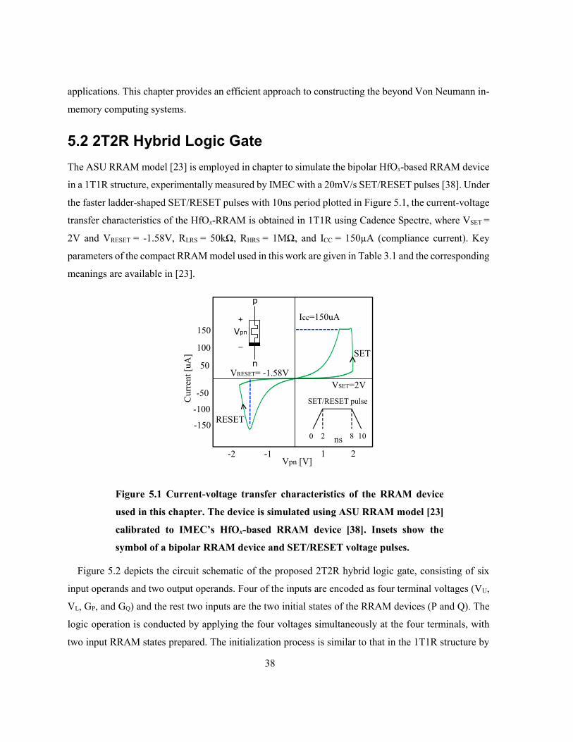
38
applications. This chapter provides an efficient approach to constructing the beyond Von Neumann in-
memory computing systems.
5.2 2T2R Hybrid Logic Gate
The ASU RRAM model [23] is employed in chapter to simulate the bipolar HfOx-based RRAM device
in a 1T1R structure, experimentally measured by IMEC with a 20mV/s SET/RESET pulses [38]. Under
the faster ladder-shaped SET/RESET pulses with 10ns period plotted in Figure 5.1, the current-voltage
transfer characteristics of the HfOx-RRAM is obtained in 1T1R using Cadence Spectre, where VSET =
2V and VRESET = -1.58V, RLRS = 50kΩ, RHRS = 1MΩ, and ICC = 150µA (compliance current). Key
parameters of the compact RRAM model used in this work are given in Table 3.1 and the corresponding
meanings are available in [23].
Figure 5.2 depicts the circuit schematic of the proposed 2T2R hybrid logic gate, consisting of six
input operands and two output operands. Four of the inputs are encoded as four terminal voltages (VU,
VL, GP, and GQ) and the rest two inputs are the two initial states of the RRAM devices (P and Q). The
logic operation is conducted by applying the four voltages simultaneously at the four terminals, with
two input RRAM states prepared. The initialization process is similar to that in the 1T1R structure by
Figure 5.1 Current-voltage transfer characteristics of the RRAM device
used in this chapter. The device is simulated using ASU RRAM model [23]
calibrated to IMEC’s HfOx-based RRAM device [38]. Insets show the
symbol of a bipolar RRAM device and SET/RESET voltage pulses.

39
simply applying SET/RESET voltages across terminal VU/VL and the middle node “M”. After the
operation, the two outputs, P’ and Q’, are in situ stored in the two nonvolatile memory cells, able to
store computation results. The logic gate concept here combines both voltage potentials and RRAM
states as input operands, defined as R/V-R hybrid logic, different from others such as R-R logic and V-
R logic. The 2T2R hybrid logic circuit can be regarded as both/either combinational circuit (when the
logic gate is used for once so that the current output P’/Q’ is only determined by the current hybrid
input (VU, VL, GP, GQ, P, Q) and/or sequential circuit (when the logic gate is used for multiple times so
that output P’/Q’ is determined by current voltage input (VU, VL, GP, GQ) and previous resistive output
P/Q).
In this chapter, high/low (0V or grounded) voltage potential represents logic “1”/“0” and RRAM
state HRS/LRS refers to logic “1”/“0”. The full utilization of computing resource enhances the
computation efficiency and flexibility significantly, one simple logic gate with six input operands. GP
and GQ are overdrive gate voltages applied to gates of the two transistors (serving as switch controls)
to reduce transistor resistance and avoid any threshold voltage drop between gate and source.
Figure 5.2 Proposed 2T2R hybrid logic (R/V-R logic) gate with two RRAMs
connected back-to-back. 2The four terminal voltages (VU, VL, GP, GQ) and two
RRAM initial states before computation (P, Q) are encoded as six input operands.
The two RRAM states after one-step computation (P’, Q’) refer to two nonvolatile
output results of the logic gate.
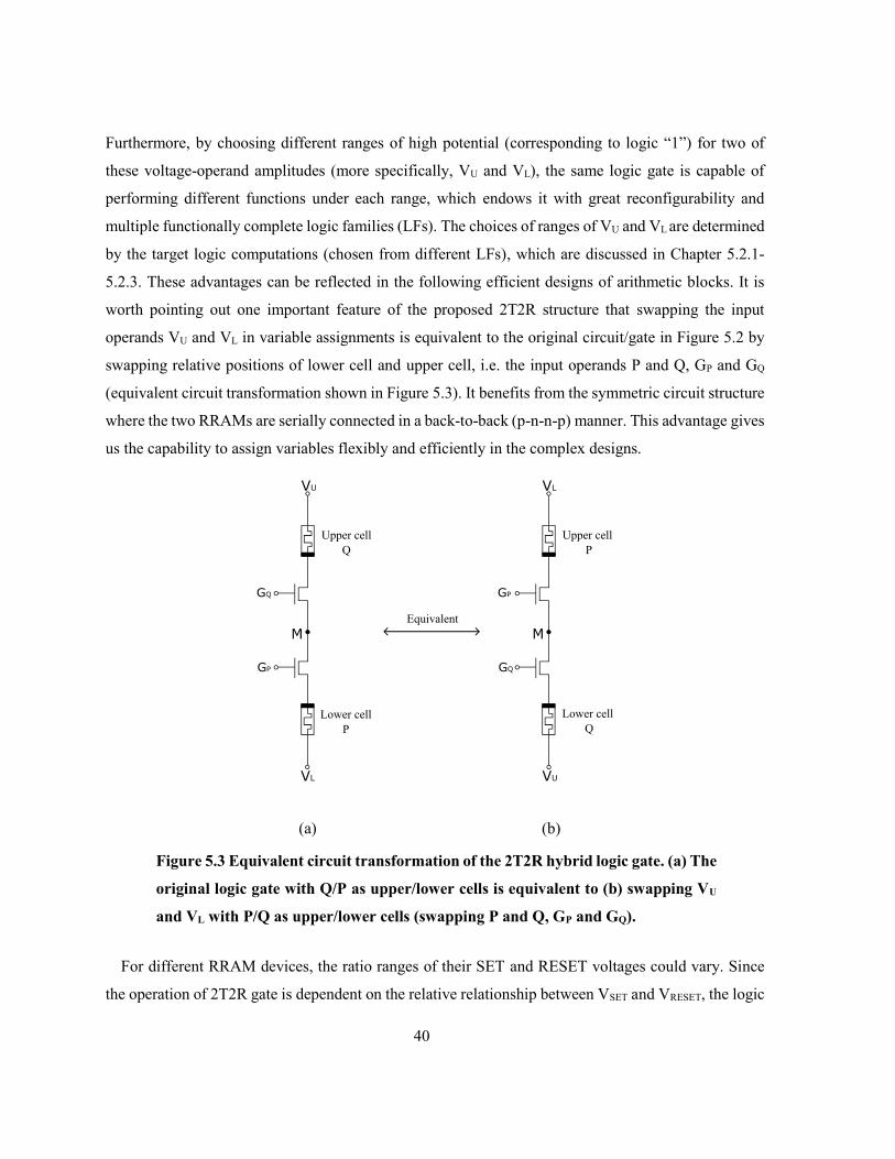
40
Furthermore, by choosing different ranges of high potential (corresponding to logic “1”) for two of
these voltage-operand amplitudes (more specifically, VU and VL), the same logic gate is capable of
performing different functions under each range, which endows it with great reconfigurability and
multiple functionally complete logic families (LFs). The choices of ranges of VU and VL are determined
by the target logic computations (chosen from different LFs), which are discussed in Chapter 5.2.1-
5.2.3. These advantages can be reflected in the following efficient designs of arithmetic blocks. It is
worth pointing out one important feature of the proposed 2T2R structure that swapping the input
operands VU and VL in variable assignments is equivalent to the original circuit/gate in Figure 5.2 by
swapping relative positions of lower cell and upper cell, i.e. the input operands P and Q, GP and GQ
(equivalent circuit transformation shown in Figure 5.3). It benefits from the symmetric circuit structure
where the two RRAMs are serially connected in a back-to-back (p-n-n-p) manner. This advantage gives
us the capability to assign variables flexibly and efficiently in the complex designs.
For different RRAM devices, the ratio ranges of their SET and RESET voltages could vary. Since
the operation of 2T2R gate is dependent on the relative relationship between VSET and VRESET, the logic
(a) (b)
Figure 5.3 Equivalent circuit transformation of the 2T2R hybrid logic gate. (a) The
original logic gate with Q/P as upper/lower cells is equivalent to (b) swapping VU
and VL with P/Q as upper/lower cells (swapping P and Q, GP and GQ).

41
gates formed by different RRAMs may have different LFs and the voltage range for each LF is different
as well. Fortunately, for any given bipolar RRAM device with different VSET and |VRESET| ratios in the
ranges of (0, 1), 1, (1, 2), 2, or (2, + ∞), the functional completeness of LFs are always available. In this
work, the hybrid logic gate and its LFs are presented based on the ASU’s model to simulate IMEC’s
RRAM device (shown in Figure 5.1), whose SET/RESET voltage ratio is
𝑉𝑆𝐸𝑇
|𝑉𝑅𝐸𝑆𝐸𝑇|=
2
.58= 1.27 ∈ (1,2). (5.1)
For other ranges of VSET/|VRESET|, i.e. (0, 1), 1, 2, and (2, + ∞), the corresponding similar LFs can be
derived in the same manner.
5.2.1 Logic Family 1 (LF1)
In LF1, the range of high potential (logic “1”) for two input voltage operands, VU and VL, is given by
𝑈, 𝐿 = 𝐿𝐹 ∈ ( 𝑆𝐸𝑇 , 2| 𝑅𝐸𝑆𝐸𝑇|). (5.2)
The complete function from inputs to outputs in this case can be derived as
𝑃′ = 𝑃 · ( 𝑈 + 𝐿 + 𝐺𝑃 + 𝐺𝑄 + 𝑄); (5.3)
𝑄′ = 𝑄 · ( 𝑈 + 𝐿 + 𝐺𝑃 + 𝐺𝑄 + 𝑃). (5.4)
To better explain the working principle of this logic gate, the above functions with a special input
combination that (VU, VL, GP, GQ) = (1, 0, 1, 1) are shown in Table 5.1. In this case, Equation (5.3) is
simplified to P’=P (bit hold) and Equation (5.4) becomes Q’=P·Q (AND). The truth table of input and
output can be obtained by analyzing the voltage divider formed by the two serial RRAM cells. A special
case when Q=1 (the initial state of upper cell prepared in HRS) is able to perform “bit transfer”
P Q P’=P Q’=P·Q0 0 0 00 1 0 01 0 1 01 1 1 1
Table 5-1 Truth table for P/Q and P’/Q’ when (VU, VL, GP, GQ) = (1, 0, 1, 1): P’=P
(bit hold), Q’=P·Q (AND). Q’=P·1 (bit transfer) operation is highlighted in
green.

42
operation copying data stored in lower cell P to upper cell Q (Q’=P), highlighted in green. The data
transfer operation is important for the logic gate cascading (copying the resistive computation result of
Logic function
𝑃 𝑃 𝑄 𝑈 𝐿 𝐺𝑃 𝐺𝑄
0 0 X X X A B
1 1 X 1 X A B
𝐴 A X 1 X X B
𝐵 B X 1 X X A
(NOT A) 1 0 0 A 1 1
(NOT B) 1 0 0 B 1 1
𝐴 + 𝐵 (OR2) 1 A B 1 1 1
+ (NAND2) 1 0 0 1 A B
𝐴𝐵 (AND2) A B 0 1 1 1
(NOR2) 0 0 B 1 1
𝐴 + (RIMP) 1 0 A B 1 1
+ 𝐵 (IMP) 1 0 B A 1 1
𝐵 (NIMP) B 0 0 A 1 1
𝐴 (RNIMP) A 0 0 B 1 1
Table 5-3 Variable assignments for 14 Boolean logics of output P’ in LF1 for
multiple input operands
Logic function
𝑃 𝑃 𝑄 𝑈 𝐿 𝐺𝑃 𝐺𝑄
𝐴 + 𝐵 + 𝐶 (OR3) 1 A B 1 1
+ + 𝐶 (NAND3) 1 0 C 1 A B
𝐴 + 𝐵 + 𝐶 + (OR4) 1 A B 1
+ + 𝐶 + (NAND4) 1 0 D A B
𝐴 + 𝐵 + 𝐶 + + (OR5)
1 A B
+ + 𝐶 + +
(NAND5)1 D A B
𝐴(𝐵 + 𝐶) A B C 1 1 1
𝐴(𝐵 + 𝐶 + ) A B C 1 1
𝐴(𝐵 + 𝐶 + + ) A B C 1
𝐴(𝐵 + 𝐶 + + + ) A B C
Table 5-2 Variable assignments for 14 Boolean logics of output P’ in LF1 for
one/two input operands
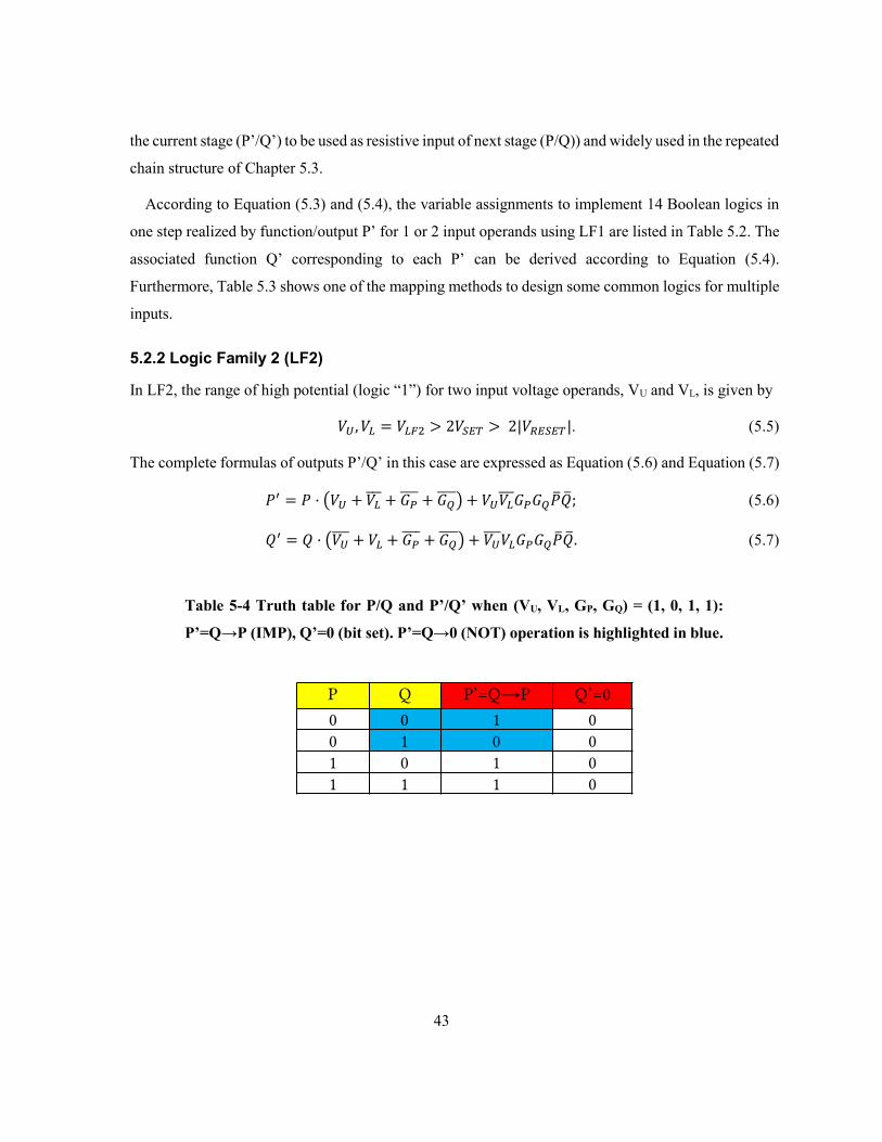
43
the current stage (P’/Q’) to be used as resistive input of next stage (P/Q)) and widely used in the repeated
chain structure of Chapter 5.3.
According to Equation (5.3) and (5.4), the variable assignments to implement 14 Boolean logics in
one step realized by function/output P’ for 1 or 2 input operands using LF1 are listed in Table 5.2. The
associated function Q’ corresponding to each P’ can be derived according to Equation (5.4).
Furthermore, Table 5.3 shows one of the mapping methods to design some common logics for multiple
inputs.
5.2.2 Logic Family 2 (LF2)
In LF2, the range of high potential (logic “1”) for two input voltage operands, VU and VL, is given by
𝑈, 𝐿 = 𝐿𝐹2 > 2 𝑆𝐸𝑇 > 2| 𝑅𝐸𝑆𝐸𝑇|. (5.5)
The complete formulas of outputs P’/Q’ in this case are expressed as Equation (5.6) and Equation (5.7)
𝑃′ = 𝑃 · ( 𝑈 + 𝐿 + 𝐺𝑃 + 𝐺𝑄 ) + 𝑈 𝐿𝐺𝑃𝐺𝑄; (5.6)
𝑄′ = 𝑄 · ( 𝑈 + 𝐿 + 𝐺𝑃 + 𝐺𝑄 ) + 𝑈 𝐿𝐺𝑃𝐺𝑄. (5.7)
P Q P’=Q→P Q’=0
0 0 1 00 1 0 01 0 1 01 1 1 0
Table 5-4 Truth table for P/Q and P’/Q’ when (VU, VL, GP, GQ) = (1, 0, 1, 1):
P’=Q→P (IMP), Q’=0 (bit set). P’=Q→0 (NOT) operation is highlighted in blue.
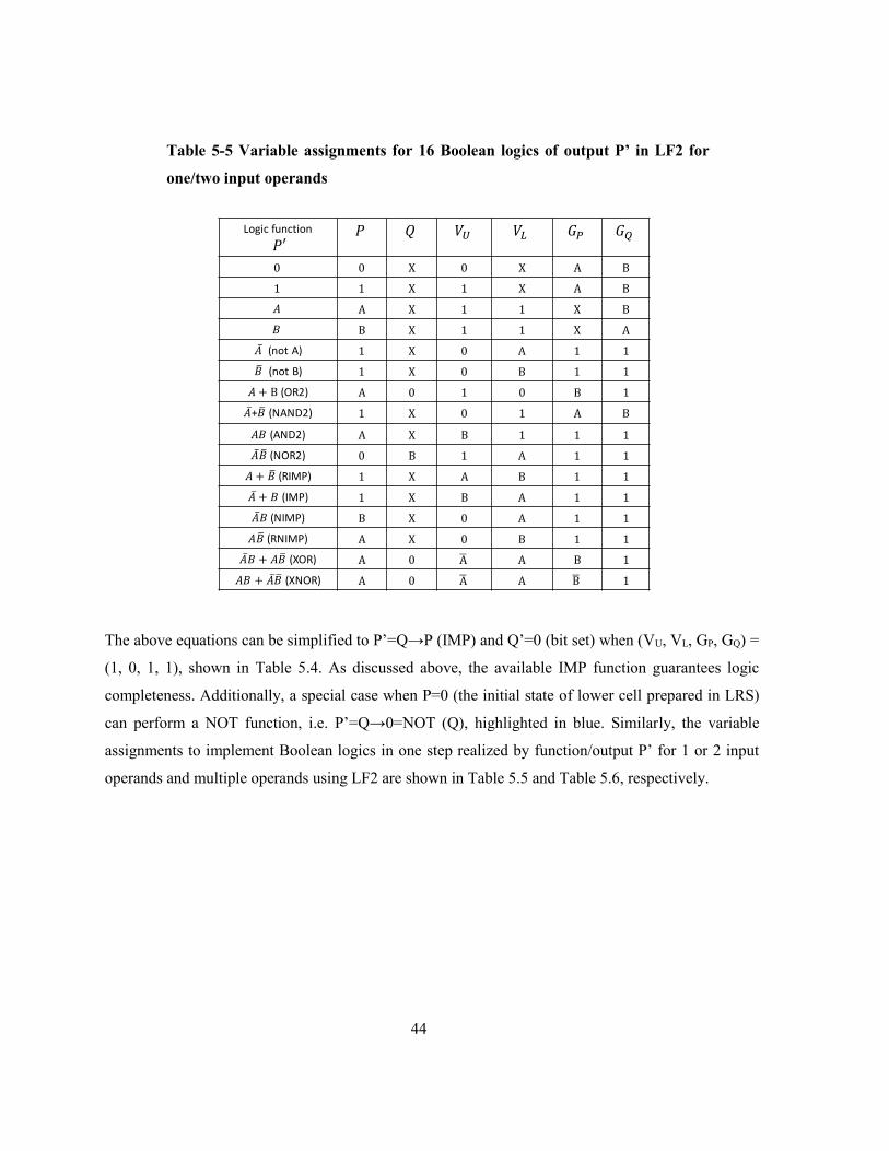
44
The above equations can be simplified to P’=Q→P (IMP) and Q’=0 (bit set) when (VU, VL, GP, GQ) =
(1, 0, 1, 1), shown in Table 5.4. As discussed above, the available IMP function guarantees logic
completeness. Additionally, a special case when P=0 (the initial state of lower cell prepared in LRS)
can perform a NOT function, i.e. P’=Q→0=NOT (Q), highlighted in blue. Similarly, the variable
assignments to implement Boolean logics in one step realized by function/output P’ for 1 or 2 input
operands and multiple operands using LF2 are shown in Table 5.5 and Table 5.6, respectively.
Logic function
𝑃 𝑃 𝑄 𝑈 𝐿 𝐺𝑃 𝐺𝑄
0 0 X 0 X A B
1 1 X 1 X A B
𝐴 A X 1 1 X B
𝐵 B X 1 1 X A
(not A) 1 X 0 A 1 1
(not B) 1 X 0 B 1 1
𝐴 + B (OR2) A 0 1 0 B 1
+ (NAND2) 1 X 0 1 A B
𝐴𝐵 (AND2) A X B 1 1 1
(NOR2) 0 B 1 A 1 1
𝐴 + (RIMP) 1 X A B 1 1
+ 𝐵 (IMP) 1 X B A 1 1
𝐵 (NIMP) B X 0 A 1 1
𝐴 (RNIMP) A X 0 B 1 1
𝐵 + 𝐴 (XOR) A 0 A B 1
𝐴𝐵 + (XNOR) A 0 A B 1
Table 5-5 Variable assignments for 16 Boolean logics of output P’ in LF2 for
one/two input operands

45
5.2.3 Logic Family 3 (LF3)
In LF3, the range of high potential (logic “1”) for two input voltage operands, VU and VL, is given by
𝑈, 𝐿 = 𝐿𝐹3 ∈ (2| 𝑅𝐸𝑆𝐸𝑇|, 2 𝑆𝐸𝑇). (5.8)
The full relationship between outputs and inputs in this case are determined as following Eq.
𝑃′ = 𝑃 · ( 𝑈 + 𝐿 + 𝐺𝑃 + 𝐺𝑄 + 𝑄) + 𝑈 𝐿𝐺𝑃𝐺𝑄; (5.9)
𝑄′ = 𝑄 · ( 𝑈 + 𝐿 + 𝐺𝑃 + 𝐺𝑄 + 𝑃) + 𝑈 𝐿𝐺𝑃𝐺𝑄. (5.10)
Similarly, in the case of (VU, VL, GP, GQ) = (1, 0, 1, 1), the functions of P’ and Q’ are presented in Table
5.7, where P’=Q→P (IMP), Q’=P·Q (AND). Under LF3, Table 5.8 and Table 5.9 are generated
according to Equation (5.9) and (5.10), summrizing the variable assignments to achieve the Boolean
logics in one step realized by function/output P’ for 1 or 2 input operands and multiple operands.
Logic function
𝑃 𝑃 𝑄 𝑈 𝐿 𝐺𝑃 𝐺𝑄
𝐴 + B + (OR3) 1 X A B 1
+ + 𝐶 (NAND3) 1 X 0 A B C
𝐴𝐵𝐶 (AND3) 0 0 A 0 B C
𝐶 (NOR3) 0 A 1 B 1
𝐴 + B + + (OR4) 1 X A B
+ + 𝐶 + (NAND4) 1 X A B C
𝐴𝐵𝐶 (AND4) 0 0 A B C
𝐶 (NOR4) 0 0 B
𝐴𝐵𝐶 (AND5) 0 A B C
𝐶 (NOR5) 0 E B
𝐴𝐵 + 𝐴𝐶 + 𝐵𝐶 (MAJ3) C 0 A B 1 1
Table 5-6 Variable assignments for common logics of output P’ in LF2 for
multiple input operands
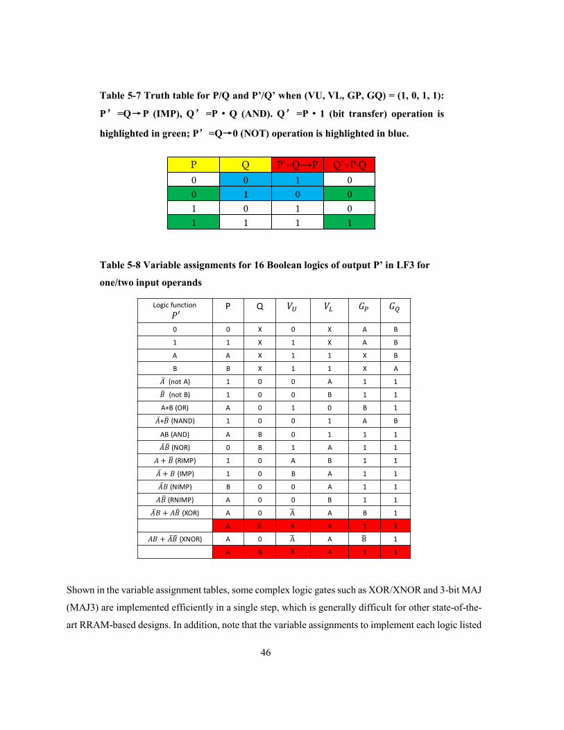
46
Shown in the variable assignment tables, some complex logic gates such as XOR/XNOR and 3-bit MAJ
(MAJ3) are implemented efficiently in a single step, which is generally difficult for other state-of-the-
art RRAM-based designs. In addition, note that the variable assignments to implement each logic listed
P Q P’=Q→P Q’=P·Q0 0 1 00 1 0 01 0 1 01 1 1 1
Logic function
𝑃 P Q 𝑈 𝐿 𝐺𝑃 𝐺𝑄
0 0 X 0 X A B
1 1 X 1 X A B
A A X 1 1 X B
B B X 1 1 X A
(not A) 1 0 0 A 1 1
(not B) 1 0 0 B 1 1
A+B (OR) A 0 1 0 B 1
+ (NAND) 1 0 0 1 A B
AB (AND) A B 0 1 1 1
(NOR) 0 B 1 A 1 1
𝐴 + (RIMP) 1 0 A B 1 1
+ 𝐵 (IMP) 1 0 B A 1 1
𝐵 (NIMP) B 0 0 A 1 1
𝐴 (RNIMP) A 0 0 B 1 1
𝐵 + 𝐴 (XOR) A 0 A B 1
A B A 1 1
𝐴𝐵 + (XNOR) A 0 A B 1
A B A 1 1
Table 5-8 Variable assignments for 16 Boolean logics of output P’ in LF3 for
one/two input operands
Table 5-7 Truth table for P/Q and P’/Q’ when (VU, VL, GP, GQ) = (1, 0, 1, 1):
P’=Q→P (IMP), Q’=P·Q (AND). Q’=P·1 (bit transfer) operation is
highlighted in green; P’=Q→0 (NOT) operation is highlighted in blue.

47
in above tables are not unique and could be designed flexibly in different ways (input operands in the
form of either voltage or RRAM state), such as the two XOR/XNOR implementations in Table 9. The
optional assignments are particularly beneficial in gate cascading, since the signals to be cascaded
should be preferred to be stored as RRAM states, eliminating the need of complicated peripheral
circuitry for signal conversion (current/RRAM state to voltage). Table 5.1, Table 5.4, and Table 5.7
provide us one efficient way to implement resistance-to-resistance stateful logic, i.e. R-R logic, utilizing
the proposed 2T2R logic gate, in which the terminal voltages (VU, VL, GP, GQ) serve as
control/operation voltages instead of input operands. The 2T2R R-R logic is crucial for the
cascadability of 2T2R hybrid logic gates as all the information in the R-R logic is stored as RRAM
states. Since any of the LFs is functionally complete, a single LF is sufficient to implement different
circuits. For instance, LF3 is used to design arithmetic blocks. Therefore, no more than two electric
voltage levels are needed, one as VLF and the other as VG, if different from VLF. In this work, all
transistors are implemented using the TSMC 65nm library with the same minimum NMOS size,
W/L=60nm/65nm, simulated in Cadence Spectre.
Logic function
𝑃 𝑃 𝑄 𝑈 𝐿 𝐺𝑃 𝐺𝑄
𝐴 + B + (OR3) 1 0 A B 1
+ + 𝐶 (NAND3) 1 0 0 A B C
𝐴𝐵𝐶 (AND3) 0 0 A 0 B C
𝐶 (NOR3) 0 A 1 B 1
𝐴 + B + + (OR4) 1 0 A B
+ + 𝐶 +
(NAND4)1 0 A B C
𝐴𝐵𝐶 (AND4) 0 0 A B C
𝐶 (NOR4) 0 0 B
𝐴 + B + + + (OR5)
1 E A B
+ + 𝐶 + + (NAND5)
1 A B C
𝐴𝐵𝐶 (AND5) 0 A B C
𝐶 (NOR5) 0 E B
𝐴𝐵 + 𝐴𝐶 + 𝐵𝐶 (MAJ3) C 0 A B 1 1
Table 5-9 Variable assignments for common logics of output P’ in LF3 for
multiple input operands

48
5.3 Arithmetic Logic Block Design
To validate the design efficiency in designing digital circuits and systems based on the proposed 2T2R
hybrid logic, arithmetic logic blocks from the simple 1-bit full adder (FA) to larger 4-bit ripple carry
adder (RCA), pipelined RCA, and fast prefix tree adder are implemented, as example circuits, in this
section. The circuit structures of all of these arithmetic blocks are regular and uniform, built by simply
replicating the 2T2R gate to form a chain structure. The interaction and cascade between these gates in
the chain are achieved through a programmable interconnect whose connection is controlled by the
gate/switch of NMOS transistors, similar to which of a SRAM-based field programmable gate array
(FPGA). Thus, the design of digital circuits is concentrated on the signal/operand assignments, data
path design, and interconnect controls on the reconfigurable architecture, rather than the circuit
topology in implementations of conventional expensive application specific integrated circuits (ASIC).
This makes it easy and cheap for design, fabrication, and integration.
5.3.1 1-bit Full Adder (FA)
As a fundamental building block of RCA and an arithmetic logic unit (ALU), the 1-bit FA is initially
implemented, which adds three binary inputs A, B, and Ci (carry in) to generate two binary outputs S
(sum) and Co (carry out). The general computing formulas of each output are given as following Eq.
𝑆 = 𝐴⊕𝐵⊕ 𝐶 = (𝐴⊕ 𝐶 ) ⊕ 𝐵 (5.11)
𝐶𝑜 = + 𝐶𝑖 + 𝐶𝑖 (5.12)
where the S is computed with two XOR operations and Co is obtained by an MAJ3 operation. From
Table 5.5/5.8 and Table 5.6/5.9, the computation of XOR and MAJ3 can be carried out with one-step
operation. As previously discussed in the 2T2R hybrid logic gate, the input operands can be either
voltage or RRAM state, while the outputs are only RRAM state. Therefore, in the cascaded
gates/multiple step operations, to avoid signal conversion from resistance to voltage, the computation
results of current gate/step are supposed to be only in the form of RRAM states as inputs of next
gate/step. The FA implementation is an example of this design rule and the reason why we calculate
𝐴⊕ 𝐶𝑖 first in the first step by assigning (𝐴, 𝐶 , , 𝐴, 1, 1) to (P, Q, VU, VL, GP, GQ) (highlighted as red
in Table 5.8), shown in Figure 5.4. The first step also computes 𝐶𝑜 (complement of carry out, similar
to the inverted carry in efficient CMOS design) concurrently by assigning (𝐶𝑖 , 0, , 𝐵, 1, 1) to (P, Q, VU,
VL, GP, GQ) according to the highlighted row in Table 10. The computation parallelism in first step is

49
achieved thanks to a pass gate (PG) transistor, separating the respective operation on two 2T2R logic
gates. The second step is simply programming the lower RRAM of the right 2T2R gate from ACi to B,
while others remain unchanged. The second XOR operation with B is carried out by assigning
(𝐵, 𝐴 ⊕ 𝐶𝑖 , , 𝐵, 1, 1) to (P, Q, VU, VL, GP, GQ) in the third step to obtain the result of S. Note that the
result of 𝐴⊕ 𝐶𝑖 of previous step shows up only as RRAM state Q in this step, while B in the form of
both voltage and RRAM state P so that no signal conversion is needed. All the intermediate results are
stored as nonvolatile RRAM states.
To summarize, the 1-bit FA can be implemented in three steps with two 2T2R hybrid logic gates,
connected by the PG NMOS to achieve the possible programmable interconnect within the adder
circuits. The connected 2T2R structure ensures that any two of the 1T1R cells in the chain can form a
2T2R hybrid logic gate to perform all the available operations, making adder cascade (carry-
propagation) easy to be implemented without complicated peripheral circuits. However, the PG
transistor does not function in the FA circuits due to the simple operations within each 2T2R gate, i.e.
no interaction required between them. It plays an important role in other more complex circuits such as
the RCA and prefix adder in the following sections.
1st step 2nd step 3rd step
𝐴
𝐵
1
1
1
10
𝐵
1
1
Figure 5.4 Full adder implementation with 2x 2T2Rs in three steps. The four RRAM-state
transitions after each step and the corresponding operation voltages are labeled. Step 1 is to
calculate ⊕ 𝒊 and . Step two is to input . Step three is to obtain .

50
5.3.2 4-bit Ripple Carry Adder (RCA)
Following the design of 1-bit FA, a 4-bit RCA is shown to validate complex arithmetic circuits,
computing [𝐴3𝐴2𝐴 𝐴 ] + [𝐵3𝐵2𝐵 𝐵 ] = [𝐶4𝑆3 𝑆2 𝑆 𝑆 ] . The circuit structure is still built by
repeating the 2T2R gate connected horizontally by PG NMOS transistors, as depicted in Figure 5.5.
Each dashed box shows the circuit schematic of 1-bit FA as the universal unit block so that an N-bit
RCA can be implemented using N 1-bit FAs. The example of 4-bit case is presented here to demonstrate
the adder operations and process.
Figure 5.7(a) shows the computation flow chart of the 4-bit RCA, which of an N-bit one could be
otained similarly. The corresponding RRAM state transition in each step is presented in Figure 5.7(b),
where the carry propagation procedure is actually conducted in two separate steps. One is for bit transfer
operation between 𝐶𝑜 (of current bit) and 1 (of more significant bit); the other for NOT operation
between 𝐶𝑜 (of current bit) and 0 (of more significant bit), after which the current 𝐶𝑜 is SET to 0.
Figure 5.6 combines them together in each carry propagation step for simplicity. An N-bit RCA requires
3N steps with (6N-1) Transistors and 4N RRAMs.
The uniform implementation of above RCA with repeated 2T2R-gate chain could be optimized to
have a more compact structure by sharing one common 4T3R unit for the sole purpose of carry
LSBMSB
1-bit FA2 2T2R gates
Figure 5.5 Schematic of a 4-bit RCA with repeated structure (2T2R chain). Each unit
shown in the dashed box is a 1-bit FA as the universal unit block.

51
computation and propagation (shown in Figure 5.6). The 4T3R carry computation unit (CCU) contains
one 2T2R (CU and CL) for carry calculation and one 1T1R (CA) to assist RCA carry propagation. The
2T2R gates (Ui and Li) in the lower sum computation units (SCUs) are used for S calculation. The
RRAM state transitions of the compact RCA with slightly customized routing are shown in Figure
5.8(a). The computation of the 4-bit addition 𝐴3𝐴2𝐴 𝐴 (0101) + 𝐵3𝐵2𝐵 𝐵 (1001) =
𝐶4𝑆3𝑆2𝑆 𝑆 (01110) needs 12 steps, conducted as a case study to validate the correctness. As plotted
in Figure 5.8(b), the summation results 𝐶4𝑆3 𝑆2 𝑆 𝑆 (01110) are stored in the cells 𝐶𝐴𝐿3𝐿2𝐿 𝐿 .
Generally, an N-bit RCA with the compact implementation could be realized efficiently in 3N steps
with (3N+4) Transistors and (2N+3) RRAMs, presenting low computation complexity.
LSBMSB
1-bit FA
1 2T2R gate
Carry Computation
Unit
Sum Computation Units
𝐿
𝐿
2
𝐿2
3
𝐿3
𝐶𝑈
𝐶𝐿 𝐶𝐴
Figure 5.6 Schematic of the optimized design of 4-bit RCA. The more compact design
saves about half of the area, with greater customization.
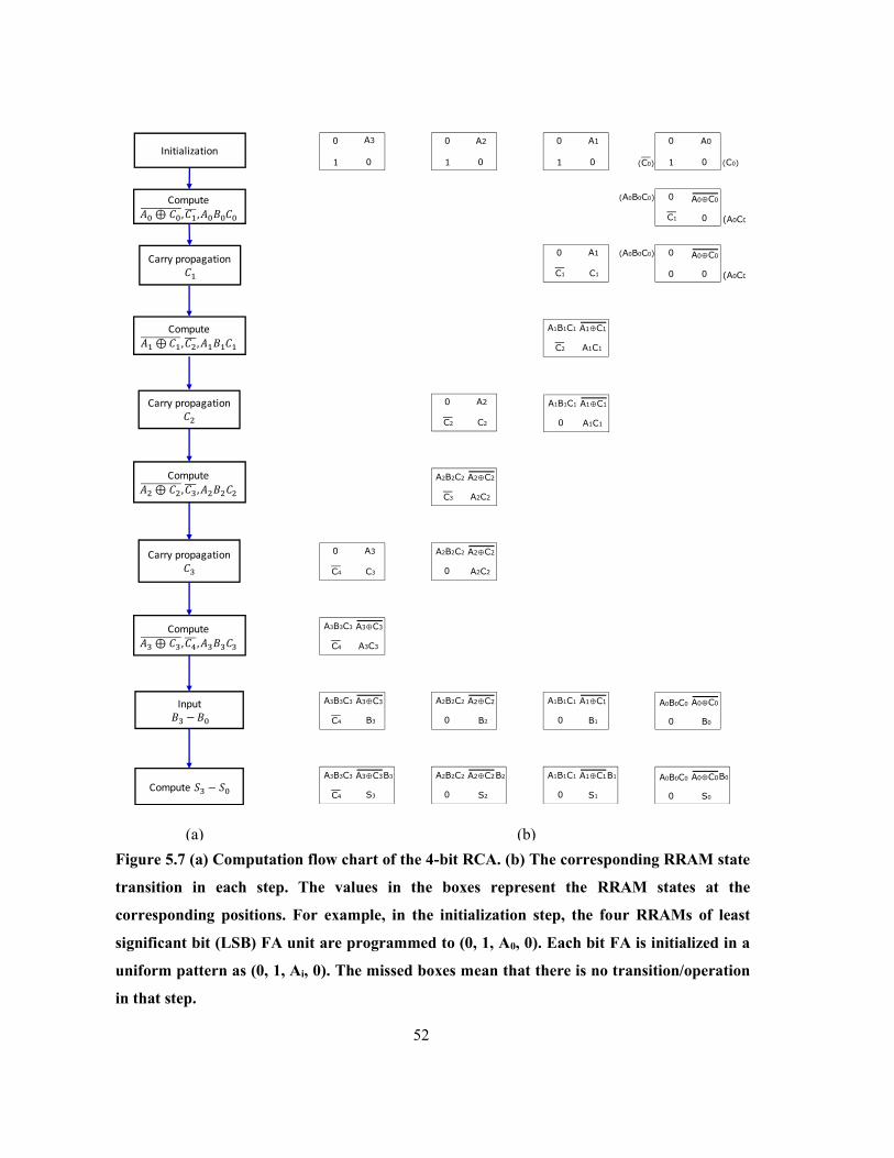
52
(a) (b)
Compute
𝐴 ⊕ 𝐶 ,𝐶 ,𝐴 𝐵 𝐶
Carry propagation𝐶
Compute
𝐴 ⊕𝐶 ,𝐶2 ,𝐴 𝐵 𝐶
Carry propagation𝐶2
Compute 𝐴2 ⊕ 𝐶2 ,𝐶3 ,𝐴2𝐵2𝐶2
Input𝐵3 −𝐵
Compute 𝑆3 − 𝑆
Initialization
Carry propagation𝐶3
Compute
𝐴3 ⊕ 𝐶3 ,𝐶4 ,𝐴3𝐵3𝐶3
Figure 5.7 (a) Computation flow chart of the 4-bit RCA. (b) The corresponding RRAM state
transition in each step. The values in the boxes represent the RRAM states at the
corresponding positions. For example, in the initialization step, the four RRAMs of least
significant bit (LSB) FA unit are programmed to (0, 1, A0, 0). Each bit FA is initialized in a
uniform pattern as (0, 1, Ai, 0). The missed boxes mean that there is no transition/operation
in that step.

53
(a) (b)
Step
0
1
0
1
0
1
0
1
0
1
0
1
0
1
0
1
0
1
0
1
0 1 2 3 4 5 6 7 8 9 10 11 12
0
1
CU
CL
CA
U3
U2
U1
U0
L3
L2
L1
L0
Step
𝐴3
𝐴2
𝐴
𝐴
𝑆3
𝑆2
𝑆
𝑆
𝐶4𝐶 𝐶 𝐶2 𝐶3
𝐵3
𝐵2
𝐵
𝐵
𝐶3
𝐶2
𝐶
𝐶
𝐶 𝐶2 𝐶3 𝐶4
Figure 5.8 (a) The RRAM state transition of the compact 4-bit RCA. The similar steps between
computing 𝟐 and computing 𝟑 ⊕ 𝟑 and 𝟒 are omitted for simplicity. (b) Simulation of
𝟑 𝟐 ( ) + 𝟑 𝟐 ( ) = 𝟒 𝟑 𝟐 ( ) as a case study to verify the
design correctness (all the transistors are at minimum 60nm widths using TSMC 65nm library). The
simulations are performed in Cadence Spectre. Two electric voltage levels are required for the RCA
operations including VLF3=VGQ=3.5V and VGP = 3V.
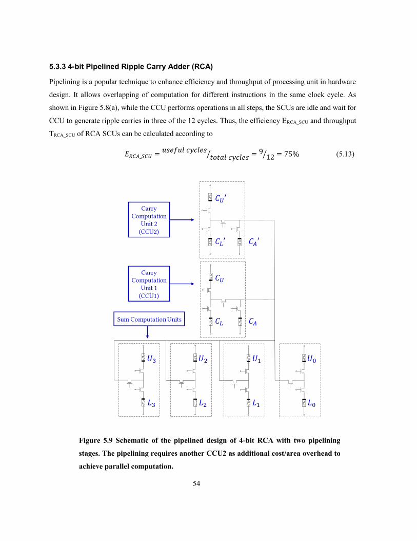
54
5.3.3 4-bit Pipelined Ripple Carry Adder (RCA)
Pipelining is a popular technique to enhance efficiency and throughput of processing unit in hardware
design. It allows overlapping of computation for different instructions in the same clock cycle. As
shown in Figure 5.8(a), while the CCU performs operations in all steps, the SCUs are idle and wait for
CCU to generate ripple carries in three of the 12 cycles. Thus, the efficiency ERCA_SCU and throughput
TRCA_SCU of RCA SCUs can be calculated according to
𝑅𝐶𝐴_𝑆𝐶𝑈 =𝑢 𝑢𝑙 𝑐𝑦𝑐𝑙
𝑡𝑜𝑡 𝑙 𝑐𝑦𝑐𝑙 ⁄ = 912⁄ = 75% (5.13)
Carry Computation
Unit 1 (CCU1)
Sum Computation Units
Carry Computation
Unit 2 (CCU2)
𝐿 𝐿 𝐿2𝐿3
2 3
𝐶𝑈
𝐶𝐿 𝐶𝐴
𝐶𝑈
𝐶𝐿 𝐶𝐴
Figure 5.9 Schematic of the pipelined design of 4-bit RCA with two pipelining
stages. The pipelining requires another CCU2 as additional cost/area overhead to
achieve parallel computation.

55
𝑅𝐶𝐴_𝑆𝐶𝑈 =# 𝑜 𝑏𝑖𝑡
𝑡𝑜𝑡 𝑙 𝑐𝑦𝑐𝑙 ⁄ = 412⁄ = 33% (5.14)
In this section, we present the pipelined 4-bit RCA implementation with two pipelining stages as a
simple case. The circuit structure is shown in Figure 5.9, requiring another CCU2 (4T3R) as additional
hardware cost/area overhead to achieve parallel computation. As in Figure 5.10, the computation of
another set of 𝐴3 𝐴2 𝐴 𝐴 (0101) + 𝐵3 𝐵2 𝐵 𝐵 (1001) = 𝐶4 𝑆3 𝑆2 𝑆 𝑆 (01110) is done in
parallel with the first 4-bit addition, adding four more steps as additional delay/latency overhead. The
efficiency Epipe_RCA_SCU and throughput Tpipe_RCA_SCU of two-stage pipelined 4-bit RCA SCUs are
boosted to 100% and 50%, respectively. For an N-bit RCA with two-stage pipelining, the efficiency is
100% and throughput is 2N/(3N+4), approaching 67% when N is larger enough (double than the non-
pipelined design). From Figure 5.10, the carry propagation cycles of CCU1 are in cycle 3/6/9 while
CCU2’s in 7/10/13. No overlapping of carry propagation between the two units guarantees the
computation concurrency due to the sharing of the common SCUs.
0
1
0
1
0
1
0
1
0
1
0
1
0
1
0
1
0
1
0
1
0 1 2 3 4 5 6 7 8 9 10 11 12 13 14 15 16 17
0
1
CU
CL
CA
U3
U2
U1
U0
L3
L2
L1
L0
Step
𝐴3
𝐴2
𝐴
𝐴
𝑆3
𝑆2
𝑆
𝑆
𝐶4𝐶 𝐶 𝐶2 𝐶3
𝐵3
𝐵2
𝐵
𝐵
𝐶3
𝐶2
𝐶
𝐶
𝐶 𝐶2 𝐶3 𝐶4
𝐶 𝑆 𝐵
𝐶 𝑆 𝐵
𝐶2 𝑆2 𝐵2
𝐶3 𝑆3 𝐵3
𝐴
𝐴
𝐴2
𝐴3
𝐴3 𝐴2 𝐴 𝐴
+ 𝐵3 𝐵2 𝐵 𝐵
= 𝑆3 𝑆2 𝑆 𝑆
0 1 0 1
+ 1 0 0 1
= 1 1 1 0
(𝐶4 𝐶3 𝐶2 𝐶 𝐶 )
( 0 0 0 1 0 )
𝐴3 𝐴2 𝐴 𝐴
+ 𝐵3 𝐵2 𝐵 𝐵
= 𝑆3 𝑆2′ 𝑆 𝑆
(𝐶4 𝐶3 𝐶2 𝐶 𝐶 )
0
1
0
1
0
1
0
1
0
1
0
1
0
1
0
1
0
1
0
1
0 1 2 3 4 5 6 7 8 9 10 11 12 13 14 15 16 17
0
1
CU
CL
CA
U3
U2
U1
U0
L3
L2
L1
L0
Step
0
1
0
1
0
1
0
1
0
1
0
1
0
1
0
1
0
1
0
1
0 1 2 3 4 5 6 7 8 9 10 11 12 13 14 15 16 17
0
1
CU
CL
CA
U3
U2
U1
U0
L3
L2
L1
L0
Step
CA’
CU’
CL’ 𝐶4 𝐶 𝐶2 𝐶3
𝐶 𝐶2 𝐶3 𝐶4
Carry propagation cycle of CCU1: 3/6/9
Carry propagation cycle of CCU2: 7/10/13
Figure 5.10 Simulation of two sets of 4-bit add computations 𝟑 𝟐 ( ) +
𝟑 𝟐 ( ) = 𝟒 𝟑 𝟐 ( ) . The pipelining requires four more steps as
additional delay/latency overhead.

56
5.3.4 4-bit Prefix Brent-Kung Adder
In the implementation of a multiple-bit RCA, the critical path, i.e. carry propagation from least
significant bit (LSB) Ci to final most significant bit (MSB) Co, limits the circuit speed because the carry
terms of each bit has dependency on carry-out of previous bit (dominates for wide adders (N>16)) [46].
Thus, the temporal complexity of either CMOS-based or RRAM-based N-bit RCA is O(N). Fast adders
generally use a tree structure for parallelism, calculating intermediate signals propagate (P) and
generate (G) as follows
𝑃 = 𝐴⊕𝐵 (5.15)
𝐺 = 𝐴𝐵 (5.16)
which have no dependencies on carry terms so that can be computed concurrently, called prefix
computation. In this section, we implement a 4-bit tree Brent-Kung adder [33] using recursive carry
lookahead to demonstrate logarithmic complexity O(log2N) of critical path based on our 2T2R hybrid
logic method.
The PG diagram of the 4-bit prefix Brent-Kung adder is shown in Figure 5.11 and the equation in
the figure describes the relationship between critical path signal C4/G3:0 and intermediate signals P and
G in this tree adder. A 2T2R hybrid logic gate is capable of calculating Pi and Gi of each bit concurrently
3 2 1 0
𝑃 𝐺 𝑃 𝐺
𝐺
𝑃2𝐺2𝑃3𝐺3
𝐺3 = 𝐶4
𝑃3 2𝐺3 2
3:0 2:0 1:0 0:0
i:j
i:j
i:k k-1:j
i:j
i:k k-1:j
i:j
Gi:k
Pk-1:j
Gk-1:j
Gi:j
Pi:j
Pi:k
Gi:k
Gk-1:j
Gi:j G
i:j
Pi:j
Gi:j
Pi:j
Pi:k
Black cell Gray cell Buffer
𝐶4 = 𝐺3 = 𝐺3 2 + 𝑃3 2𝐺 = (𝐺3+𝑃3𝐺2) + 𝑃3𝑃2(𝐺 + 𝑃 𝐺 )
Figure 5.11 PG diagram of a 4-bit prefix Brent-Kung adder and its PG notations. The
calculation of C4/G3:0 is the critical path in this tree adder whose formula is shown as the
equation.

57
in a single step by assigning (𝐴 , 𝐵 , 𝐴𝑖 , 𝐴 , 1, 1) to (P, Q, VU, VL, GP, GQ)), in which the Pi/Gi are stored
in the lower/upper cell, shown in Figure 5.12(a). The circuit schematics of the 4-bit Brent-Kung adder
are presented in Figure 5.12(b), requiring five 2T2R gates connected by four PG NMOS transistors.
Figure 5.12(c) gives the simulation results of critical path calculation when performing the 4-bit
addition 𝐴3𝐴2𝐴 𝐴 (0101) + 𝐵3𝐵2𝐵 𝐵 (1001) = 𝐶4𝑆3 𝑆2 𝑆 𝑆 (01110). The final result C4/G3:0=0
is stored in cell L4 and can be used for further calculations. Note that in the prefix Brent-Kung adder,
the C4 is obtained in the 6th cycle, while it is done in 10th cycle in the RCA implementation (Figure
5.8(b). The improved performance is due to the parallel processing algorithm of each bit. Similarly, for
an N-bit Brent-Kung adder, it can be derived that the critical-path delay is proportional to log2N, same
as the CMOS designs.
5.4 Design Evaluation and Comparison
Demonstrated by various implementations of arithmetic logic blocks such as 4-bit RCA, pipelined
RCA, and prefix tree adder, the proposed 2T2R hybrid logic is a promising and efficient approach to
L0/U0
L1
U1/L2U3/L4
L3
U4
0 1 2 3 4 5 6 Step
10
10
10
10
10
10
U2
𝐴3
𝑃 𝐺 𝐴 𝐵
𝐴
𝐵 𝐴2𝐵3 0
𝐵2
0
𝑃
𝐿
𝐿
𝐿2 3 𝐿4
2
𝐿3
4
𝐺 𝑃2𝐺3 𝑃3 2
𝐺2
𝑃3 𝑃3 + 𝐺2
𝑃 + 𝐺
𝐺 𝑃2𝐺3 𝑃3 2
𝐺 −𝐺3 2 −
− −− 𝑃3 2𝐺
𝐺3 2
− −− 𝟒
0
𝐿 𝐿 𝐿2𝐿3
2 3 4
𝐿4
𝐴
𝐵
𝐴
𝐴
1
1
𝑃
𝐺
(a)
(b) (c)
Figure 5.12 (a) PG calculation implemented in one step on a 2T2R hybrid logic gate. (b) Circuit
schematic (five 2T2R gates connected by four PG NMOS transistors) of 4-bit Brent-Kung adder.
(c) Simulation results of critical path calculation when performing 𝟑 𝟐 ( ) +
𝟑 𝟐 ( ) = 𝟒 𝟑 𝟐 ( ).

58
designing RRAM-based in-memory computing system. The small RRAM cell in the circuit serves as
both logic device and storage unit. The 2T2R gate chain connected by horizontal PG NMOS transistors
is able to implement any logic block with the same uniform and repeated circuit structure. This feature
endows it with programmability and reconfigurability, similar to that of an FPGA. It allows us to
program/re-program the chain to realize different designs, significantly simplifying the implementation
and fabrication of digital circuits and systems.
In this section, the performance of the arithmetic units is evaluated and compared to the CMOS
circuits and other state-of-the-art RRAM designs, based on their computational complexity, more
specifically, spatial complexity and temporal complexity. In a RRAM-based system, spatial complexity
Device Technology
ReRAM − e t e si e ( ) 5
𝐴 − A e ( 2) 100 (4 2)
CMOS − ( ) 65
𝐴 − ( 2) 8450 (2 2)
0
2
4
6
8
10
Static Mirror TG
Are
a [μ
m2]
Area comparison for
32-bit Adder design
87%75%
Compact RCAThis work
RCA
Table 5-10 Device technology used for design evaluation
Figure 5.13 Area comparison of this work with CMOS designs for a 32-bit adder.
The RCA of this work saves ~75% area from mirror adder and TG-based adder,
while the compact RCA saves ~87% area.
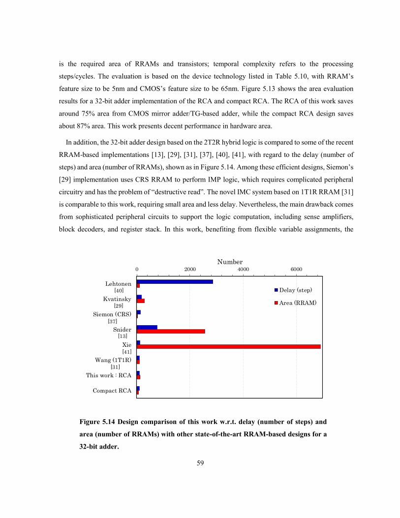
59
is the required area of RRAMs and transistors; temporal complexity refers to the processing
steps/cycles. The evaluation is based on the device technology listed in Table 5.10, with RRAM’s
feature size to be 5nm and CMOS’s feature size to be 65nm. Figure 5.13 shows the area evaluation
results for a 32-bit adder implementation of the RCA and compact RCA. The RCA of this work saves
around 75% area from CMOS mirror adder/TG-based adder, while the compact RCA design saves
about 87% area. This work presents decent performance in hardware area.
In addition, the 32-bit adder design based on the 2T2R hybrid logic is compared to some of the recent
RRAM-based implementations [13], [29], [31], [37], [40], [41], with regard to the delay (number of
steps) and area (number of RRAMs), shown as in Figure 5.14. Among these efficient designs, Siemon’s
[29] implementation uses CRS RRAM to perform IMP logic, which requires complicated peripheral
circuitry and has the problem of “destructive read”. The novel IMC system based on 1T1R RRAM [31]
is comparable to this work, requiring small area and less delay. Nevertheless, the main drawback comes
from sophisticated peripheral circuits to support the logic computation, including sense amplifiers,
block decoders, and register stack. In this work, benefiting from flexible variable assignments, the
0 2000 4000 6000
Lehtonen
Kvatinsky
Siemon (CRS)
Snider
Xie
Wang (1T1R)
This work : RCA
Compact RCA
Number
State-of-the-art RRAM-based 32-bit Adders
Delay (step)
Area (RRAM)
[40]
[29]
[37]
[13]
[41]
[31]
Figure 5.14 Design comparison of this work w.r.t. delay (number of steps) and
area (number of RRAMs) with other state-of-the-art RRAM-based designs for a
32-bit adder.

60
designs are able to avoid unnecessary signal conversions therefore eliminates the need of complicated
peripheral circuits [47].
5.5 Readout Structure
After the computation is completed, the final results stored in the RRAM cells might need to be readout.
The readout process of the 3T2R chain can be designed by placing two units of readout circuitry, such
as a current sense amplifier (CSA) or a transimpedance amplifier (TIA), on top and bottom positions
of the chain, shown in Fig. 8. During the read process, all horizontal pass gate transistors are ON (the
red path). Then, apply a read voltage Vread (e.g. 100mV) on the middle nodes (“In” node in the chain).
The read-cell selection (read enable control) is achieved by the gate control of each 1T1R, similar to
the function of column mux in the conventional SRAM memory arrays. The readout circuitry acts as a
current to voltage converter to sense the ILRS/ IHRS (0/1) of the selected cell.
Figure 5.15 Readout structure of the 3T2R chain. During read process, all PG transistors are
ON and a Vread is applied on the middle nodes. Other NMOS transistors in each 1T1R control
the read-cell selection (read enable control).
61
5.6 Conclusions
This chapter proposes an efficient in-memory computing scheme based on hybrid logic in 2T2R RRAM
whose programmable logic functionality is determined by the amplitude of voltage operands and
variable assignments. The hybrid-logic method fully utilizes the computing resource in a RRAM-based
structure, which can be potentially adopted similarly in other computational-memory enabled systems.
Various logic families are available to be used to design digital circuits flexibly. A repeated, uniform,
and reconfigurable 2T2R-gate chain with programmable interconnects is designed to efficiently
implement any arithmetic logic block. The example circuits such as ripple carry adder, its pipelined
implementation, and parallel prefix adder are shown to validate the hybrid-logic design methodology.
The computing principle is discussed and the arithmetic circuits are compared with CMOS designs and
popular post-CMOS systems based on their spatial complexity and temporal complexity. The overall
result shows superior performance of this work in designing efficient digital circuits and systems.

62
Chapter 6
Conclusions and Future Work
6.1 Conclusions
This thesis has reported two efficient computing/logic methodologies for beyond von Neumann
processing-in-memory applications by fully exploring a proposed regular, symmetric 2T2R circuit
structure. The first scheme implements digital logic in a stateful manner, in which the computation
operands are represented by nonvolatile RRAM states and logic functionality is determined by
amplitudes of external operation voltages. The second scheme leverages computing resource of the
circuit in a hybrid manner, by encoding both RRAM states and operation voltages as inputs. The two
schemes are designed to implement their corresponding logic gates (logic families) based on the unified
2T2R gate and further build arithmetic building blocks of an ALU using a reconfigurable 3T2R (2T2R
gate) chain structure with programmable interconnections.
The proposed circuit structure and computation methodologies make it easy to design, develop, and
fabricate digital circuits and systems based on CMOS technology and post-CMOS but CMOS-
compatible RRAM technology. Common digital units such as full adder, ripple-carry adder, pipelined
ripple-carry adder, and parallel carry look-ahead adder are designed and evaluated to validate the
efficient implementations. The work is compared to the mature CMOS designs and other RRAM
systems with respect to its computational complexity, i.e. speed and area. It presents advantages in
hardware area relative to CMOS circuits and in both area and speed as well as peripheral circuitry
compared to popular RRAM designs. The in-memory operations are simple and clean, meanwhile the
circuit structures are regular and symmetric, requiring no signal conversions during whole compute
process. The result of each scheme could build a technology cell library that can be potentially used as
input to a technology-mapping algorithm. The proposed stateful-logic and hybrid-logic methodologies
present prospect of hardware acceleration and future beyond-von Neumann in-memory computing
architectures.

63
6.2 Future Work
The results of this work point to a number of potential directions to extend the scope of this project.
Since the electrical designs are only implemented at the level of front end based on simulation, one
important future work is to realize the physical design part including the layout design, fabrication, and
experimental testing in order to complete the design flow and further realize the practical digital circuits
and integrated dense memory array.
Future work also includes
(1) designing new RRAM-enabled emerging circuit architectures;
(2) exploring logical methods and principles based on other post-CMOS technologies;
(3) embedding computational memories including RRAM into the commercial mature CMOS
technology so as to leverage their advantages such as non-volatility, small area, and scalability
to improve the performance of current circuits and systems;
(4) using nonvolatile memory to achieve hardware acceleration in the ASIC and FPGA platform;
(5) addressing and improving the classic RRAM issues including reliability and endurance and
analyzing how these problems affect the system-level performance, to design fault-tolerant
circuits and systems.
The in-memory processing schemes based on the regular and symmetric 2T2R structure proposed by
this work present the prospect in hardware implementation of post-CMOS and beyond-von-Neumann
computing systems. The result of the study could build a technology library that can be potentially used
as standard cell library for ASIC digital designs. The highly integrated 3-D stacked arrays could be
widely adopted in the future applications of dense nonvolatile data storage and emerging in-memory
processors.

64
Bibliography
[1] Sze, Vivienne, et al. "Hardware for machine learning: Challenges and opportunities." 2017
IEEE Custom Integrated Circuits Conference (CICC). IEEE, 2017.
[2] Malik, Maria, et al. "Architecture exploration for energy-efficient embedded vision
applications: From general purpose processor to domain specific accelerator." 2016 IEEE
Computer Society Annual Symposium on VLSI (ISVLSI). IEEE, 2016.
[3] Rajendran, Bipin, and Fabien Alibart. "Neuromorphic computing based on emerging memory
technologies." IEEE Journal on Emerging and Selected Topics in Circuits and Systems 6.2
(2016): 198-211.
[4] Arcas-Abella, Oriol, et al. "Hardware acceleration for query processing: leveraging FPGAs,
CPUs, and memory." Computing in Science & Engineering 18.1 (2015): 80.
[5] Sklyarov, Valery, et al. "Analysis and comparison of attainable hardware acceleration in all
programmable systems-on-chip." 2015 Euromicro Conference on Digital System Design.
IEEE, 2015.
[6] Shafique, Muhammad, et al. "Cross-layer approximate computing: From logic to
architectures." Proceedings of the 53rd Annual Design Automation Conference. ACM, 2016.
[7] Vetter, Jeffrey S., and Sparsh Mittal. "Opportunities for nonvolatile memory systems in
extreme-scale high-performance computing." Computing in Science & Engineering 17.2
(2015): 73-82.
[8] Yu, Shimeng. "Neuro-inspired computing with emerging nonvolatile memorys." Proceedings
of the IEEE 106.2 (2018): 260-285.
[9] Imani, Mohsen, Saransh Gupta, and Tajana Rosing. "Ultra-efficient processing in-memory for
data intensive applications." Proceedings of the 54th Annual Design Automation Conference
2017. ACM, 2017.
[10] Ahn, Junwhan, et al. "A scalable processing-in-memory accelerator for parallel graph
processing." ACM SIGARCH Computer Architecture News 43.3 (2016): 105-117.
65
[11] Ielmini, Daniele, and H-S. Philip Wong. "In-memory computing with resistive switching
devices." Nature Electronics 1.6 (2018): 333.
[12] Wong, H-S. Philip, and Sayeef Salahuddin. "Memory leads the way to better
computing." Nature nanotechnology 10.3 (2015): 191.
[13] Borghetti, Julien, et al. "‘Memristive’switches enable ‘stateful’logic operations via material
implication." Nature464.7290 (2010): 873.
[14] Cassinerio, Marco, N. Ciocchini, and Daniele Ielmini. "Logic computation in phase change
materials by threshold and memory switching." Advanced Materials 25.41 (2013): 5975-5980.
[15] Jeong, Doo Seok, et al. "Memristors for energy‐efficient new computing
paradigms." Advanced Electronic Materials 2.9 (2016): 1600090.
[16] Ney, A., et al. "Programmable computing with a single magnetoresistive
element." Nature 425.6957 (2003): 485.
[17] Bohr, Mark T., and Ian A. Young. "CMOS scaling trends and beyond." IEEE Micro 37.6
(2017): 20-29.
[18] Javey, Ali, et al. "Ballistic carbon nanotube field-effect transistors." nature 424.6949 (2003):
654.
[19] Chen, An. "A review of emerging non-volatile memory (NVM) technologies and
applications." Solid-State Electronics 125 (2016): 25-38.
[20] Wendin, G. "Quantum information processing with superconducting circuits: a
review." Reports on Progress in Physics 80.10 (2017): 106001.
[21] Shalf, John M., and Robert Leland. "Computing beyond moore's law." Computer 48.SAND-
2015-8039J (2015).
[22] Wong, H-S. Philip, et al. "Metal–oxide RRAM." Proceedings of the IEEE 100.6 (2012): 1951-
1970.
[23] Chen, Pai-Yu, and Shimeng Yu. "Compact modeling of RRAM devices and its applications in
1T1R and 1S1R array design." IEEE Transactions on Electron Devices 62.12 (2015): 4022-
4028.

66
[24] Chen, Wei-Hao, et al. "Circuit design for beyond von Neumann applications using emerging
memory: From nonvolatile logics to neuromorphic computing." 2017 18th International
Symposium on Quality Electronic Design (ISQED). IEEE, 2017.
[25] Ielmini, Daniele. "Brain-inspired computing with resistive switching memory (RRAM):
Devices, synapses and neural networks." Microelectronic Engineering 190 (2018): 44-53.
[26] Zidan, Mohammed A., and Wei D. Lu. "RRAM fabric for neuromorphic and reconfigurable
compute-in-memory systems." 2018 IEEE Custom Integrated Circuits Conference (CICC).
IEEE, 2018.
[27] Balatti, Simone, Stefano Ambrogio, and Daniele Ielmini. "Normally-off logic based on
resistive switches—Part I: Logic gates." IEEE Transactions on Electron Devices 62.6 (2015):
1831-1838.
[28] Kvatinsky, Shahar, et al. "MAGIC—Memristor-aided logic." IEEE Transactions on Circuits
and Systems II: Express Briefs61.11 (2014): 895-899.
[29] Kvatinsky, Shahar, et al. "Memristor-based material implication (IMPLY) logic: Design
principles and methodologies." IEEE Transactions on Very Large Scale Integration (VLSI)
Systems22.10 (2013): 2054-2066.
[30] Wang, Zhuo-Rui, et al. "Functionally complete Boolean logic in 1T1R resistive random access
memory." IEEE Electron Device Letters 38.2 (2016): 179-182.
[31] Wang, Zhuo-Rui, et al. "Efficient implementation of Boolean and full-adder functions with
1T1R RRAMs for beyond von Neumann in-memory computing." IEEE Transactions on
Electron Devices 99 (2018): 1-8.
[32] Linn, E., et al. "Beyond von Neumann—logic operations in passive crossbar arrays alongside
memory operations." Nanotechnology 23.30 (2012): 305205.
[33] Truong, Son Ngoc, and Kyeong-Sik Min. "New memristor-based crossbar array architecture
with 50-% area reduction and 48-% power saving for matrix-vector multiplication of analog
neuromorphic computing." Journal of semiconductor technology and science 14.3 (2014):
356-363.
[34] Shafiee, Ali, et al. "ISAAC: A convolutional neural network accelerator with in-situ analog
arithmetic in crossbars." ACM SIGARCH Computer Architecture News 44.3 (2016): 14-26.

67
[35] Wang, Zhuo-Rui, et al. "Functionally complete Boolean logic in 1T1R resistive random access
memory." IEEE Electron Device Letters 38.2 (2016): 179-182.
[36] Xia, Qiangfei, et al. "Memristor− CMOS hybrid integrated circuits for reconfigurable
logic." Nano letters 9.10 (2009): 3640-3645.
[37] Siemon, Anne, et al. "A complementary resistive switch-based crossbar array adder." IEEE
journal on emerging and selected topics in circuits and systems 5.1 (2015): 64-74.
[38] Chen, Yang Yin, et al. "Balancing SET/RESET Pulse for $>\hbox 10^10 $ Endurance in
$\hbox HfO _ 2\hbox /Hf $ 1T1R Bipolar RRAM." IEEE Transactions on Electron
devices 59.12 (2012): 3243-3249.
[39] Predictive Technology Model (PTM): http://ptm.asu.edu/.
[40] Lehtonen, Eero, and Mika Laiho. "Stateful implication logic with memristors." 2009
IEEE/ACM International Symposium on Nanoscale Architectures. IEEE, 2009.
[41] Xie, Lei, et al. "Fast boolean logic mapped on memristor crossbar." 2015 33rd IEEE
International Conference on Computer Design (ICCD). IEEE, 2015.
[42] Yang, Zongxian, and Lan Wei. "Logic Circuit and Memory Design for In-Memory Computing
Applications using Bipolar RRAMs." 2019 IEEE International Symposium on Circuits and
Systems (ISCAS). IEEE, 2019.
[43] Li, Haitong, et al. "Resistive RAM-centric computing: Design and modeling
methodology." IEEE Transactions on Circuits and Systems I: Regular Papers 64.9 (2017):
2263-2273.
[44] Kvatinsky, Shahar, et al. "MRL—Memristor ratioed logic." 2012 13th International Workshop
on Cellular Nanoscale Networks and their Applications. IEEE, 2012.
[45] Ielmini, Daniele. "Resistive switching memories based on metal oxides: mechanisms,
reliability and scaling." Semiconductor Science and Technology 31.6 (2016): 063002.
[46] Chang, T-Y., and M-J. Hsiao. "Carry-select adder using single ripple-carry adder." Electronics
letters 34.22 (1998): 2101-2103.

68
[47] Yang, Zongxian, Yixiao Ma, and Lan Wei. "Functionally Complete Boolean Logic and Adder
Design Based on 2T2R RRAMs for Post-CMOS In-Memory Computing." Proceedings of the
2019 on Great Lakes Symposium on VLSI. ACM, 2019.
[48] Balatti, Simone, Stefano Ambrogio, and Daniele Ielmini. "Normally-off logic based on
resistive switches—Part II: Logic circuits." IEEE Transactions on Electron Devices 62.6
(2015): 1839-1847.
[49] Prezioso, Mirko, et al. "Training and operation of an integrated neuromorphic network based
on metal-oxide memristors." Nature 521.7550 (2015): 61.
[50] Chen, Wei-Hao, et al. "Circuit design for beyond von Neumann applications using emerging
memory: From nonvolatile logics to neuromorphic computing." 2017 18th International
Symposium on Quality Electronic Design (ISQED). IEEE, 2017.
[51] Jain, Shubham, et al. "Computing in memory with spin-transfer torque magnetic ram." IEEE
Transactions on Very Large Scale Integration (VLSI) Systems 26.3 (2017): 470-483.
[52] Li, Shuangchen, et al. "Pinatubo: A processing-in-memory architecture for bulk bitwise
operations in emerging non-volatile memories." Proceedings of the 53rd Annual Design
Automation Conference. ACM, 2016.
[53] Cho, Kyoungrok, Sang-Jin Lee, and Kamran Eshraghian. "Memristor-CMOS logic and digital
computational components." Microelectronics Journal 46.3 (2015): 214-220.
[54] Jiang, Tao, et al. "Understanding the behavior of in-memory computing workloads." 2014
IEEE International Symposium on Workload Characterization (IISWC). IEEE, 2014.
[55] Yakopcic, Chris, Md Zahangir Alom, and Tarek M. Taha. "Memristor crossbar deep network
implementation based on a convolutional neural network." 2016 International Joint
Conference on Neural Networks (IJCNN). IEEE, 2016.


