
Low-consuming class D amplifier for
rough environments Master Thesis in electronics at Mälardalen University conducted for
Salvator HB
Robin Pettersson
Sahag Normanian
3/31/2011
Abstract
This project consists of designing a class D amplifier and selecting a proper speaker to use
with it. Focus lies on high soundpressure, low powerconsumption and a wide operating
temperature range. The current version of the amplifier uses a self-oscillating modulator, a
full-bridge power stage and a second order passive low-pass Butterworth filter. Project
specifications were not met with the current setup, but suggested improvements can be
found in the report.

2
Contents
1 Introduction .......................................................................................................................................... 5
1.1 Project Specifications .................................................................................................................. 5
1.2 Report Organization ...................................................................................................................... 7
2 Background ........................................................................................................................................... 8
2.1 Common Power Amplifier Classes................................................................................................. 8
2.1.1 Class A ..................................................................................................................................... 8
2.1.2 Class B ..................................................................................................................................... 8
2.1.3 Class AB .................................................................................................................................. 8
2.1.4 Class C ..................................................................................................................................... 9
2.2 Class D Amplification ..................................................................................................................... 9
2.2.1 Basic Concepts of Class D Amplifiers ...................................................................................... 9
2.2.2 Advantages and Disadvantages of Class D ........................................................................... 10
2.4 The Modulation Stage ................................................................................................................. 11
2.4.1 Pulse Width Modulation (PWM) .......................................................................................... 12
2.4.2 Pulse Density Modulation (PDM) ......................................................................................... 12
2.4.3 Self-Oscillating Modulation and Pulse Position Modulation (PPM) ..................................... 13
2.5 The Power Stage .......................................................................................................................... 14
2.5.1 Half-Bridge ............................................................................................................................ 14
2.5.2 Full-Bridge............................................................................................................................. 14
2.5.3 A Comparison Between Half-Bridge And Full-Bridge ........................................................... 15
2.6 The Filtering Stage ....................................................................................................................... 16
2.6.1 Low-Pass Filter ...................................................................................................................... 17
2.7 Speaker Selection ........................................................................................................................ 18
3 Preliminary Design and Construction ............................................................................................. 18
3.1 The Modulationstage ................................................................................................................. 19
3.1.1 The Pulse Width Modulator ............................................................................................... 19
3.1.2 PCB Layout ............................................................................................................................ 21
3.2 The Power stage .......................................................................................................................... 21
3.2.1 Amplifier Configuration ........................................................................................................ 22
3.2.2 MOSFET Selection ................................................................................................................. 22
3.2.3 Gate Drivers .......................................................................................................................... 23
3.2.4 PCB Layout ............................................................................................................................ 25
3.3 The Filtering Stage ....................................................................................................................... 26

3
3.3.1 Filter Components ................................................................................................................ 27
3.4 Speaker ........................................................................................................................................ 28
4 Preliminary Results ............................................................................................................................. 29
4.1 Functionality Testing ................................................................................................................... 29
4.1.1 The Modulationstage ........................................................................................................... 29
4.1.2 The Power stage ................................................................................................................... 29
4.1.3 The Filtering Stage ................................................................................................................ 30
4.2 Problems And Improvements ...................................................................................................... 30
5 Improved Design And Construction ................................................................................................... 32
5.1 Changing Speaker ........................................................................................................................ 32
5.2 The Modulationstage .................................................................................................................. 32
5.2.1 Self-Oscillating Modulator .................................................................................................... 32
5.2.2 Breadboard- And PCB Layout ............................................................................................... 35
5.3 The Power stage .......................................................................................................................... 36
5.4 The Filtering Stage ....................................................................................................................... 37
6 Improved Version Results ................................................................................................................... 37
6.1 Functionality Testing ................................................................................................................... 37
6.1.1 The Modulationstage ........................................................................................................... 37
6.1.2 The Power stage ................................................................................................................... 39
6.1.3 The Filtering Stage ................................................................................................................ 40
6.1.4 Full system Assembly ............................................................................................................ 41
6.2 Speaker Testing ........................................................................................................................... 41
6.2.1 Listening Test ........................................................................................................................ 41
6.2.2 Soundpressure ...................................................................................................................... 41
6.3 Power Consumption .................................................................................................................... 43
7 Problems With The Improved Version ............................................................................................... 45
8 Conclusion .......................................................................................................................................... 46
9 Improvements And Future Work ....................................................................................................... 48
9.1 The Modulation stage ................................................................................................................. 48
9.2 The Power Stage .......................................................................................................................... 48
9.3 The Filtering Stage ....................................................................................................................... 49
9.4 Pre-amplification Stage ............................................................................................................... 49
9.5 General Improvements................................................................................................................ 50
References ............................................................................................................................................. 51
Appendix A ............................................................................................................................................ 53
4
Appendix B ............................................................................................................................................ 56
Appendix C............................................................................................................................................. 82
Appendix D ............................................................................................................................................ 91
Appendix E ............................................................................................................................................. 92
Appendix F ............................................................................................................................................. 95
Appendix G ............................................................................................................................................ 96
5
1 Introduction In many parts of the electronics industry the trend leans towards smaller, more mobile and
more energy efficient products, whether it may involve making a TV thinner, or extending
the battery-life on a laptop. The same goes for the electronics used in audio applications.
MP3-players need better audio quality and higher output power while maintaining a small
size. Outdoor sound systems need to be playing music at longer distances without using
extremely large amplifiers. All this, while still keeping powerconsumption at a minimum
level. This is where the class D audio amplifier comes in.
The class D audio amplifier uses a switching technique that results in a much higher
efficiency than traditional amplifier topologies. With higher efficiency, less power is
converted to heat and thus the size of the cooling unit can be greatly reduced or removed
completely. The high efficiency also makes the class D audio amplifier very suitable for
battery powered solutions, greatly extending the runtime on a single charge.
These features open up endless possibilities for the class D audio amplifier, often providing a
more energy efficient and practical solution than traditional audio amplifiers.
1.1 Project Specifications
This project consists of two parts; Designing and constructing a class D amplifier and
selecting a proper speaker to use with it. Project specifications as given by the company
Salvator HB is presented in table 1.
The major thing to have in mind when designing the class D audio amplifier for this project is
that this amplifier is not intended for applications where high quality audio is needed. The
main reason for that are the types of speakers that will be used. The horn-speakers used in
these applications are capable of producing sound at very high pressure but has a narrow
frequency response. That means that they can only produce audio at a small range of
frequencies.
The other major concern is that the amplifier is intended to run on batteries, therefore
power consumption needs to be low. The idea was to use only one battery, but with the
possibility of adding one extra if necessary. The second battery however is in use by another

6
circuit which leaves dual supply as a last resort. One important notice is that the amplifier
should be able to operate for at least 60 minutes at full power. In this case it means that
sound is being played for a few seconds at a time, with several minutes of silence between
each interval.
Another important notice is the audioquality mentioned in table 1. “Audible difference” is a
somewhat vague specification. It was therefore decided that the sound-pressure at a
distance of 200 meters from the speaker should be equal to that of a normal conversation,
approximately 60dB1.
Finally, as the title states, the amplifier should be able to operate in rough environments.
This basically comes down to the temperature range the amplifier should be able to operate
in, as casing and weather-protection was not part of the project specifications. The amplifier
should be able to operate in temperatures ranging from -30 to +30 degrees Celsius (Swedish
climate).
Table 1: Project specifications
1 http://www.physicsclassroom.com/class/sound/u11l2b.cfm, 2011-02-03
Specifikation Value Output power, soundpressure Approx. 60 Watts, 60dB @ 200 meters
Minimum runtime Approx. 60 minutes @ full power
Powersupply One battery; 12V, 5Ah
Audioquality Audible difference between gunshot and explosion @ 200 meters from speaker, mono
audio
Connectors and levers RCA and 3.5mm input connectors, volumeknob
Temperature range (°C) -30 - +30
Speaker Horn, 6-8Ω, IP65-classified
7
1.2 Report Organization
This report follows the progress of each step made throughout the project. Chapter 2 gives
the reader a bit of background on the subject of amplifiers in general and class D amplifiers
in particular. Chapter 3 describes the process of designing and constructing the preliminary
design and chapter 4 discusses some of the results from testing the preliminary design, as
well as improvements that will be made. Chapter 5 shows the construction of the second
revision of the amplifier while chapter 6 discusses further testing of both the amplifier and
the selected speaker. Finally chapter 7 sums up all the conclusions made in the project and
chapter 8 discusses further improvements needed.

8
2 Background
2.1 Common Power Amplifier Classes
The basic idea of an amplifier is that it receives a signal from some kind of input source and
provides a larger version of that signal to either another amplifier stage or some output
device2. While the properties of small-signal amplifiers usually consists of amplification
linearity and magnitude of gain, large-signal amplifiers or power amplifiers main features are
the circuit´s power efficiency and the impedance matching to the output device.
Below follows some of the basic classes of power amplifiers. Though several more exists,
these are generally not used for basic audio purposes.
2.1.1 Class A
Class A uses 100% of the input signal. This means that the active element (often bipolar
transistors or MOSFETs) remains conducting all of the time3. Since class A amplifiers are
relatively easy to construct and more linear than other classes, they are mostly used in
small-signal applications were efficiency is not a consideration; i.e. as headphone amplifiers.
2.1.2 Class B
In class B amplifiers only 50% of the input signal is used, which means that the active
element works in its linear range half of the time and remains “turned off” the other half.
Most class B amplifiers uses two output devices that each conducts one half cycle of the
input signal. This however leads to some troubling issues if the transition from one active
element to the other is not perfect. This result in errors referred to as crossover distortion.
2.1.3 Class AB
As the name suggests, class AB amplifiers provides an operating point somewhere between
class A and class B. The two active elements in class AB conduct more than half of the cycle
each, which is a way to try to minimize crossover distortion of class B amplifiers.
2 Boylestad, ”Introductory Circuit Analysis”, Tenth Edition, 1996, page 701
3 http://en.wikipedia.org/wiki/Electronic_amplifier, 2010-10-03
9
2.1.4 Class C
Class C uses less than 50% of the input signal for each output device, resulting in high
crossover distortion but potentially higher efficiency.
2.2 Class D Amplification
Class D amplifiers is not something that is entirely new, it has been around for the last 15-20
years but is not as widespread as Class A, B, AB and C topologies4. Historically, class D
amplifiers were used in a limited number of applications such as motor controllers, because
it was more difficult to generate the high quality signals demanded for audio applications.
This however has changed and class D amplifiers have advanced sufficiently to be able to
function in high-end audio products.
2.2.1 Basic Concepts of Class D Amplifiers
The basic concept with class A, B, AB and C amplifiers, as discussed earlier, is that one of the
output devices conduct at any given time. This behavior results in power dissipation since a
small current must pass through the transistor even if there is no output. When the output
voltage increases, at some point in regards to given supply rails the voltage drop across the
transistor will fall, but the current increases. When the transistors saturate, the voltage from
collector to emitter or from drain to source will be low but the current will be high. In other
words, at low power levels, there will be a large voltage drop but the current is small. This
ultimately leads to a power dissipation curve that is not linear with output power. Class A
and B amplifiers thus have a point where maximum efficiency is reached, about 25% and
78% respectively.
In class D on the other hand, the amplifier works by rapidly switching the output devices
between “on” and “off”, rather than working in the linear region of the transistors or
MOSFETs. This means that when in the off state, the amplifier behaves like an open-circuit,
therefore the voltage will be the total supply rails and only a very small current will flow. In
the on state, a specific current will flow through the mechanism, dependant on output
power, and there will be no voltage present from drain to source, which gives theoretically
4 http://sound.westhost.com/articles/pwm.htm, 2010-10-06
10
zero power dissipation. This gives class D amplifiers almost 100% efficiency, in theory at
least. Although, in practice results of up to 96% has been achieved5.
The entire class D audio amplifier consists of roughly three stages: The modulation stage that
modulates the input sine wave into “digital” pulses, the power stage that does all the
switching and amplification and finally the filtering stage that filters out the high frequency
pulses from the modulation stage.
2.2.2 Advantages and Disadvantages of Class D
The most prominent advantage of the class D amplifier, when comparing to topologies such
as class A, B, AB and C, is the increased power efficiency6. This is very useful in high power
applications when small improvements in efficiency results in large decrease in waste heat
coming from the amplifier. This reduction in heat serves particularly well for low power
applications, most often entirely removing the need for heat sinks and therefore reducing
the overall size of the amplifier unit. Since the overall size of the amplifier unit is decreased,
costs associated with the enclosure can be reduced.
Although class D amplifiers have been around for many years, they only recently became
more widely used in high quality audio applications. This is because class D amplifiers have a
number of disadvantages making them less suitable for audio amplification. This was
however a bigger issue a couple of years ago, since recent advancements in technology has
solved many of the problems associated with class D audio amplification.
A well-known disadvantage with class D amplifiers is the large amount of high-frequency
noise produced by the switching design mentioned earlier. It is therefore very important to
keep the noise at a frequency that is much higher than that of the signal to be amplified, to
keep the noise out of the audible region. In this way, it is possible to filter out the high
frequency pulses with a simple low pass, passive filter. This however adds complexity,
weight and cost to the entire amplifier. Although not that big of an issue, these things have
to be taken into account.
5 http://www.irf.com/whats-new/nr071002.html, 2010-10-06
6 Briana, M. “Class D Audio Amplifier the design of a live audio Class D audio amplifier with greater than 90%
efficiency and less than 1% distortion”, 2008

11
Another disadvantage of class D amplifiers is the potentially complex design. This is
something that may result in higher expenses and increased design time. High design
expenses may be acceptable if it results in lower manufacturing costs, because
manufacturing expenses are recurring whereas design is a singular expense.
The last major disadvantage of class D amplifiers is, or more correctly was, distortion. High
THD or Total Harmonic Distortion indicates high levels of noise, which is something that
significantly detracts from the overall audio quality of the output audio. However, faster
modulation techniques have significantly reduced THD to well below one percent.
2.4 The Modulation Stage
All class D modulation techniques work by encoding the input audio signal into a stream of
pulses7. In most cases, the amplitude of the input audio signal is linked to the pulse width
and the audio, as well as unwanted high-frequency noise, is contained in the spectrum of the
pulses.
Several methods exist for modulating the signal in a class D audio amplifier. Some are better
than others in regards to simplicity, availability and effectiveness. All these requirements
must be taken into account when constructing the modulation stage. Simplicity is important
because a portable and light weight design is appealing when dealing with several amplifiers
in one system and when navigating rough environments. Effectiveness is important since the
modulation is essential to sound quality and to keep the distortion as low as possible. Finally,
availability is important when developing an independent product where some modulation
techniques would be too impractical to use. The three most common techniques to use are
PWM, PDM and self-oscillating modulation.
7 http://www.eetimes.com/design/audio-design/4015790/Class-D-Audio-Amplifiers-What-Why-and-How--Part-
5, 2010-10-06

12
2.4.1 Pulse Width Modulation (PWM)
Pulse width modulation or PWM is the most commonly used modulation technique. It
basically involves using a comparator to compare the input signal with a triangular or
ramping waveform that runs at a fixed carrier frequency. The result is a pulse-train that runs
at the fixed frequency of the carrier signal. Within that period of the carrier, the pulse width
of the PWM changes proportionally to the amplitude of the input audio signal. If the
amplitude of the audio signal exceeds the amplitude of the triangular waveform, something
called full modulation occurs. This is when the duty ratio within individual periods is either
100% or 0%.
There are a couple of advantages with using PWM in audio amplifiers. PWM allows 100 dB,
or even better, audio-band SNR (Signal to Noise Ratio) when using a carrier frequency of
only a few hundred kHz. This frequency is also low enough to limit losses in the output stage
due to the switching mechanism. It is possible to achieve almost 100% percent modulation
due to the high stability in most PWM modulators, permitting high output power up to the
point of overloading, at least in concept.
There is however a few drawbacks with using PWM. In many implementations, PWM has the
disadvantage of adding distortion8. Second, harmonics of the carrier frequency may produce
EMI (Electro Magnetic Interference) somewhere within the AM radio band. Finally there is
the problem with the pulse widths of the PWM near full modulation. When the pulses
become very small, the output stage gate-driver cannot switch properly due to the extreme
speed needed to produce these short pulses. This ultimately leads to an output power that is
somewhat lower than the theoretical maximum.
2.4.2 Pulse Density Modulation (PDM)
Another alternative to PWM is pulse density modulation or PDM. In this method, the
number of pulses in a predefined time window is relative to the common value of the input
audio signal9. One form of PDM is 1 bit sigma-delta modulation. Sigma-delta modulation
8 Nielsen, K., "A Review and Comparison of Pulse-Width Modulation (PWM) Methods for Analog and Digital
Input Switching Power Amplifiers”, 1997 9 http://www.eetimes.com/design/audio-design/4015790/Class-D-Audio-Amplifiers-What-Why-and-How--Part-
5?pageNumber=0, 2010-10-06
13
provides an advantage over PWM in regards to EMI. This is because much of the high
frequency energy in sigma-delta modulation is distributed over a wide range of frequencies,
as opposed to PWM where noise is concentrated in tones at the fixed carrier frequency and
its multiples. Since typical PDM clock frequencies lay around 3-6 MHz, these are way out of
the audible region and easily filtered out.
Sigma-delta also has the advantage that the minimum pulse width is one sampling-clock
period, even when approaching full modulation of a signal. Although safe operation up to
theoretical full power is achievable, conventional 1-bit sigma-delta modulators are only
stable to about 50% and therefore not widely used in class D amplifiers. Also, to achieve
sufficient SNR, at least 64- oversampling is needed.
2.4.3 Self-Oscillating Modulation and Pulse Position Modulation (PPM)
The not so widely used self-oscillating modulation, or sometimes called sliding mode control,
is a form of VSC (Variable Structure Control)10. This method basically consists of applying a
high-frequency switching control to a nonlinear system in order to alter its dynamics.
Amplifiers using self-oscillating modulation always use a feedback loop that determines the
switching frequency of the modulator, instead of an externally provided clock. An advantage
compared to PWM is that the high-frequency energy is often more evenly distributed.
Thanks to the feedback loop it is possible to achieve very high quality audio, but
synchronization with other switching circuits is problematic because of the loop being self-
oscillating. This also means that digital audio first needs to be converted to analog in order
to be used in an amplifier using self-oscillating modulation.
Another method for signal modulation is pulse position modulation (PPM). Here, the pulses
are of uniform amplitude and width but the position of each pulse varies with the amplitude
of the input signal11. One self-oscillating circuit, producing a pulse density modulated output,
is easily built using the standard LMC555-timer.
10
http://en.wikipedia.org/wiki/Sliding_mode_control, 2010-10-15 11
http://www.argospress.com/Resources/CommunicationsSystems/pulpositimodula.htm, 2011-01-26

14
2.5 The Power Stage
After the input signal has been modulated into pulses it needs to be amplified. There are
basically two ways of doing this, a half-bridge or a full-bridge (sometimes called H-bridge)
configuration. The bridge circuit most often consists of MOSFETs for the switching part and
some kind of gate driver powering the MOSFETs. This switching design ensures very high
efficiency in class D amplifiers.
2.5.1 Half-Bridge
In a half-bridge configuration, two MOSFETs are used but only one is turned on at every
time-instance. Figure 2.1 shows a simple half-bridge with separate drivers for each MOSFET.
The modulator and filtering stages have been left out.
Figure 2.1: A basic Half-Bridge Amplifying Stage
This kind of circuit is very simple and can provide a sufficient solution if audio quality is not a
major concern.
2.5.2 Full-Bridge
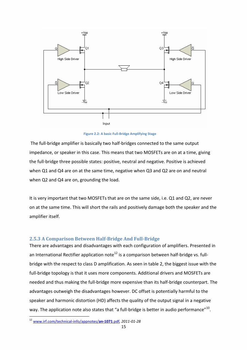
The full-bridge or H-bridge amplifier is another common configuration. Figure 2.2 shows the
basic configuration for a full-bridge amplifier. As with the previous figure, the modulator and
filter stages have been left out for easier understanding.
15
Figure 2.2: A basic Full-Bridge Amplifying Stage
The full-bridge amplifier is basically two half-bridges connected to the same output
impedance, or speaker in this case. This means that two MOSFETs are on at a time, giving
the full-bridge three possible states: positive, neutral and negative. Positive is achieved
when Q1 and Q4 are on at the same time, negative when Q3 and Q2 are on and neutral
when Q2 and Q4 are on, grounding the load.
It is very important that two MOSFETs that are on the same side, i.e. Q1 and Q2, are never
on at the same time. This will short the rails and positively damage both the speaker and the
amplifier itself.
2.5.3 A Comparison Between Half-Bridge And Full-Bridge
There are advantages and disadvantages with each configuration of amplifiers. Presented in
an International Rectifier application note12 is a comparison between half-bridge vs. full-
bridge with the respect to class D amplification. As seen in table 2, the biggest issue with the
full-bridge topology is that it uses more components. Additional drivers and MOSFETs are
needed and thus making the full-bridge more expensive than its half-bridge counterpart. The
advantages outweigh the disadvantages however. DC offset is potentially harmful to the
speaker and harmonic distortion (HD) affects the quality of the output signal in a negative
way. The application note also states that “a full-bridge is better in audio performance”10.
12
www.irf.com/technical-info/appnotes/an-1071.pdf, 2011-01-28

16
Half-Bridge Full-Bridge Supply Voltage 0,5 x 2ch 1
Current ratings 1 2
MOSFET 2 MOSFETs/channel 4 MOSFETs/channel
Gate driver 1 Gate Driver/channel
2 Gate Drivers/channel
Linearity Even and odd order HD
No even order HD
DC Offset Adjustment is needed
Can be canceled out
Modulation Pattern
2 level 3 level can be implemented
Table 2: Half-Bridge vs. Full-Bridge
2.6 The Filtering Stage
Since the signal from the amplifying stage is a modulated pulse train, it is often mandatory to
use a filter, although the output modulation may be adapted so that the amplifier may be
connected to the speaker without the use of a filter. This is called filterless class D13. This
form of class D amplifiers can many times be used, provided the wire to the speaker is less
than about 10 cm. One must however distinguish between filterless class D and class D
without filter, the last one mentioned not being recommended since it will reduce battery
life and possibly damage the speaker.
There are basically to types of filters, active or passive. Active filters use amplifying elements
such as operational amplifiers to synthesize the desired characteristics of the filter14. Gains
and drawbacks of active filters are mostly related to the operational amplifier that is used.
I.e. op amps provide high input impedance and low output impedance but limitations in
bandwidth and noise generated by the amplifying circuit may lead to unwanted results or
pricy filter-designs. Passive filters on the other hand require no power supplies and do not
have the same bandwidth limitations as active filters do. However, the components used in
passive filters can be expensive if high accuracy is needed and passive filters provide no
signal gain.
13
http://www.eetimes.com/design/audio-design/4015895/Class-D-amplifier-FAQ--Part-1-Overview-amplifier-selection-and-filters?pageNumber=2, 2010-10-15 14 Kerry, L., “A Basic Introduction to Filter-- Active, Passive, and Switched-Capacitor”, 1991
17
When designing a filter for the class D amplifier, it is important that components are chosen
carefully. The ideal case would be to design a filter that has no effect on the desired output
signal while filtering out all the high frequency noise coming from the switching
mechanism15. Since switching noise is of much higher frequency than the audio signal, the
best filter to use would be a low-pass topology. It is also desirable to have as flat pass-band
as possible when filtering audio signals, therefore the best filter type would be a
Butterworth filter.
When designing filters for class D amplifiers, one must also consider impedance matching to
the speaker used. The cut-off frequency of the filter is directly dependant on the impedance
of the speaker. Therefore is it not possible to swap speakers with different impedances
without first recalculating the values of the filter components.
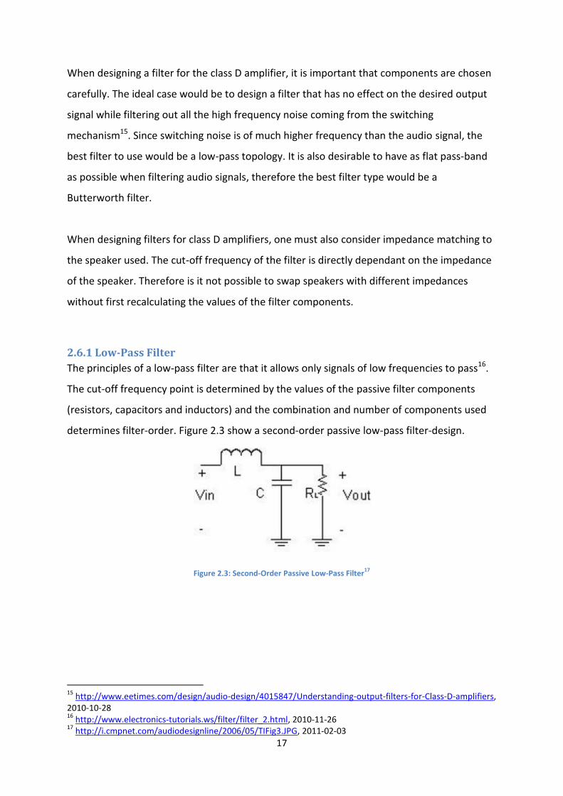
2.6.1 Low-Pass Filter
The principles of a low-pass filter are that it allows only signals of low frequencies to pass16.
The cut-off frequency point is determined by the values of the passive filter components
(resistors, capacitors and inductors) and the combination and number of components used
determines filter-order. Figure 2.3 show a second-order passive low-pass filter-design.
Figure 2.3: Second-Order Passive Low-Pass Filter17
15
http://www.eetimes.com/design/audio-design/4015847/Understanding-output-filters-for-Class-D-amplifiers, 2010-10-28 16
http://www.electronics-tutorials.ws/filter/filter_2.html, 2010-11-26 17
http://i.cmpnet.com/audiodesignline/2006/05/TIFig3.JPG, 2011-02-03
18
2.7 Speaker Selection
As stated in table 1, the speaker to be used in the project was to be of horn-type. The major
advantage with horn speakers is that the horn increases the overall efficiency of the driving
element18. This means that the acoustic output of a specific driver is increased using the
horn. Horn speakers also have the advantage of directing the sound towards a single spot, in
other words altering the horizontal and vertical coverage angels of the soundwave
emanating from the speaker. This is important when the speaker is far away from the
intended “listening position”.
In order to achieve the desired 60dB at a distance of 200 meters from the speaker, specified
in table 1, the sound pressure close to the speaker needs to be calculated using the following
equations, were L1 is the sound pressure at a distance r1 close to the speaker and L2 the
sound pressure at a distance r2 further away:
r1 = 1 m
r2 = 200 m
L1 = Unknown
L2 = 60dB
This means that the speaker must be able to output a sound pressure level of 106 dB in
order to be considered.
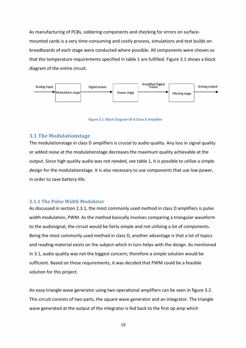
3 Preliminary Design and Construction The following section describes all the steps involved in designing and building the first
version of the class D audio amplifier, from simulation to PCB.
Since almost all class D amplifiers consist of three stages (modulation, amplification and
filter) the overall outline of the amplifier was more or less settled. Although the final design
was going to be a single card with all stages included, it was determined that the best way to
simplify error-handling was to construct each stage separately.
18
http://en.wikipedia.org/wiki/Horn_loudspeaker, 2011-02-28
19
As manufacturing of PCBs, soldering components and checking for errors on surface-
mounted cards is a very time-consuming and costly process, simulations and test builds on
breadboards of each stage were conducted where possible. All components were chosen so
that the temperature requirements specified in table 1 are fulfilled. Figure 3.1 shows a block
diagram of the entire circuit.
3.1 The Modulationstage
The modulationstage in class D amplifiers is crucial to audio quality. Any loss in signal quality
or added noise at the modulationstage decreases the maximum quality achievable at the
output. Since high quality audio was not needed, see table 1, it is possible to utilize a simple
design for the modulationstage. It is also necessary to use components that use low power,
in order to save battery-life.
3.1.1 The Pulse Width Modulator
As discussed in section 2.3.1, the most commonly used method in class D amplifiers is pulse
width modulation, PWM. As the method basically involves comparing a triangular waveform
to the audiosignal, the circuit would be fairly simple and not utilizing a lot of components.
Being the most commonly used method in class D, another advantage is that a lot of topics
and reading-material exists on the subject which in turn helps with the design. As mentioned
in 3.1, audio quality was not the biggest concern; therefore a simple solution would be
sufficient. Based on these requirements, it was decided that PWM could be a feasible
solution for this project.
An easy triangle wave generator using two operational amplifiers can be seen in figure 3.2.
This circuit consists of two parts, the square wave generator and an integrator. The triangle
wave generated at the output of the integrator is fed back to the first op amp which
Figure 3.1: Block Diagram Of A Class D Amplifier

20
functions as a comparator, comparing the signal at the positive input with GND on the
negative input.
Figure 3.2: Triangle Wave Generator Using Operational Amplifiers19
The amplitude of the triangle wave is set by the ratio R2/R120. It is very important that R2 is
larger than R1 in order for this circuit to function. The values of C and Rt affect the frequency
of the triangle wave. The full equation for the operating frequency is:
The triangle wave will act as a carrier for the audio and needs to have a frequency of at least
twice the highest frequency present in the audio signal21. In order to determine the required
output frequency of the triangle wave, the dynamic range of the audio signal must be taken
into account. The human ear can detect pressure changes in the air if they are in the audible
region, which ranges from approximately 20 Hz – 20 kHz22. Because of this, there is no need
to try to sample audio with frequencies higher than 20 kHz.
19
http://www.play-hookey.com/analog/images/square_triangle_gen.gif, 2011-01-25 20
http://www.play-hookey.com/analog/triangle_waveform_generator.html, 2011-01-25 21
http://en.wikipedia.org/wiki/Nyquist_rate, 2011-01-25 22
http://hyperphysics.phy-astr.gsu.edu/hbase/sound/earsens.html, 2011-01-25

21
Components were chosen so that a sampling-frequency of approximately 173 kHz was
achieved, giving a sampling rate of 8.65. Since the amplifier should run on single supply if
possible, instead of dual supply required by the circuit in figure 3.1, the two operational
amplifiers needed a virtual ground of half the supply-voltage at their grounded input23.
The complete modulator used a quad op amp (OPA4350) for the triangle wave generator, a
high-speed comparator (TLV3501) to compare the audio with the triangle wave and a LDO
voltage-regulator (LM1117IMD) to provide the ICs with 5 V and the required virtual ground
of 2.5 V, see appendix A. If designed correctly, the modulator should provide pulses that
change in width when the amplitude of the input audio changes.
3.1.2 PCB Layout
The problem with the first version of the modulator was that several components did not
exist in the library of the used simulation tool, Multisim. Therefore, the modulator was
constructed directly on a PCB using EAGLE, a cad-tool for developing PCBs, and the mill at
the university. Figure 3.3 shows the PCB for the modulator.
3.2 The Power stage
The power stage consists of two key-components, the MOSFETs and the gate drivers.
Choosing the correct components and using the appropriate power stage configuration is
essential to the overall performance of the amplifier.
23
http://www.swarthmore.edu/NatSci/echeeve1/Ref/SingleSupply/SingleSupply.html, 2011-01-25
Figure 3.3: PCB-Layout Of The Pulse Width Modulator
22
3.2.1 Amplifier Configuration
As discussed in section 2.4, there are two different configurations to consider when
constructing the power stage, the half-bridge and the full-bridge. Section 2.4.3 clearly states
the benefits of using a full-bridge configuration instead of the half-bridge. Important aspects
such as the ability to use a single power rail, elimination of DC offset and less distortion
clearly outweighs the drawback of the increased cost involved in using the full-bridge.
3.2.2 MOSFET Selection
Choosing the correct MOSFET is essential to the overall performance of the amplifier and the
output power produced. Parameters to consider when choosing MOSFET for this application
are the peak drain-source voltage (VDS) it can handle, the continuous drain current (ID), the
drain-source resistance (RDS(on)), the total gate charge (Qg) and rise- and fall-times (tr and tf).
Peak Voltage And Drain Current
Table 1 state that the system must be able to deliver an average of 60 Watts into an 8 Ω
speaker, therefore surviving peaks of up to 120 Watts. Since the project specifications in
table 1 states that a 12V supply should be used if possible, the MOSFETs must be able to
handle a lot of current. The current can be derived from the following equations:
U = 12V
P = 120 Watts
Based on this result, the MOSFET must be able to handle 10A peak drain current. Should
however the opportunity rise to be able to increase rail voltage, the current required would
be significantly lower. Using the same peak power and speaker impedance, but only focusing
on peak voltage, the equation yields:
R = 8 Ω
P = 120 Watts

23
In this case, the MOSFETs must be able to handle a 44V rail in order to be considered.
Selecting the right MOSFET for this application was not an easy task. Several MOSFETs meet
the peak voltage and continuous drain current requirement and there is really not much
difference between them. The final pick was International Rectifiers IRF7665 stated to be
“optimized for Class-D audio amplifier applications”24. This MOSFET has relatively low drain-
source resistance and gate charge while maintaining fast rise- and fall-times. The ability to
handle a high drain-source voltage of 100 V and drain current of maximum 14.4 A allows for
increased power output without the need of changing MOSFET.
3.2.3 Gate Drivers
Components originating from the same manufacturer often work very well together. Since
the MOSFET used in the power stage is manufactured by International Rectifier, the best
choice would be to use an International Rectifier gate driver to charge the MOSFETs. Once
again, there is an ocean of ICs to choose from. One however stands out, the IRS20124S. This
driver has programmable dead time which will be very useful in order to minimize shoot-
through and optimize harmonic distortion.
These specific gate drivers use external resistors to set dead-time and over-current (OC)
threshold, see appendix B for gate driver datasheet. Appropriate resistor values were chosen
according to the suggestions shown in table 3, to obtain the shortest possible dead time
(DT1). Resistor values used were R1 = 8,2kΩ and R2 = open.
24
See MOSFET datasheet, appendix C

24
OC threshold is set by three additional resistors, see figure 3.5. The threshold is set to allow
a maximum current of 10 A to flow to the speaker. This can later on be adjusted simply by
recalculating the values.
Values for the resistors can be derived from the following equations25:
ITRIP = ±10A
RDS(ON) = 51 mΩ
25
See Gate Driver datasheet, appendix B
Table 3: Suggested Resistor Values For Dead Time Settings
Figure 3.4: Dead time External Resistor Configuration
Figure 3.5: OC Threshold External Resistor Configuration

25
After calculating theoretical values, real world values were identified:
R3 = 9.76 kΩ
R4 = 0,560 kΩ
R5 = 1,69 kΩ
One important notice is that the equations in the datasheet for the gate drivers are
incorrect. RDS(ON) should be in mΩ, not in µΩ as used in the datasheet.
3.2.4 PCB Layout
Since the MOSFETs and gate drivers are surface mounted, the power stage has to be
fabricated on a PCB. This was done the same way as with the pulse width modulator, using
EAGLE and the PCB mill at the university.
One problem that arose during the design of the PCB was that some components did not
exist in the library of EAGLE, specifically the gate driver and the MOSFETs. Therefore new
components had to be made, which was a bit time consuming since none of the group-
members had ever tried this before.
Using the mill at the university gave room for errors in the board-design; since the waiting
time for a new PCB was significantly shorter than if each new revision had to be ordered.
Although, waiting times was a bit longer for the first revision since none of the team
members were familiar with the PCB mill.
As mentioned in section 3, each stage was constructed separately for easier error handling.
The power stage is divided in a high- and low-side which each accept a positive square-wave.
Figure 3.6 shows the PCB for the power stage. The complete schematic of the power stage
can be viewed in appendix A.
26
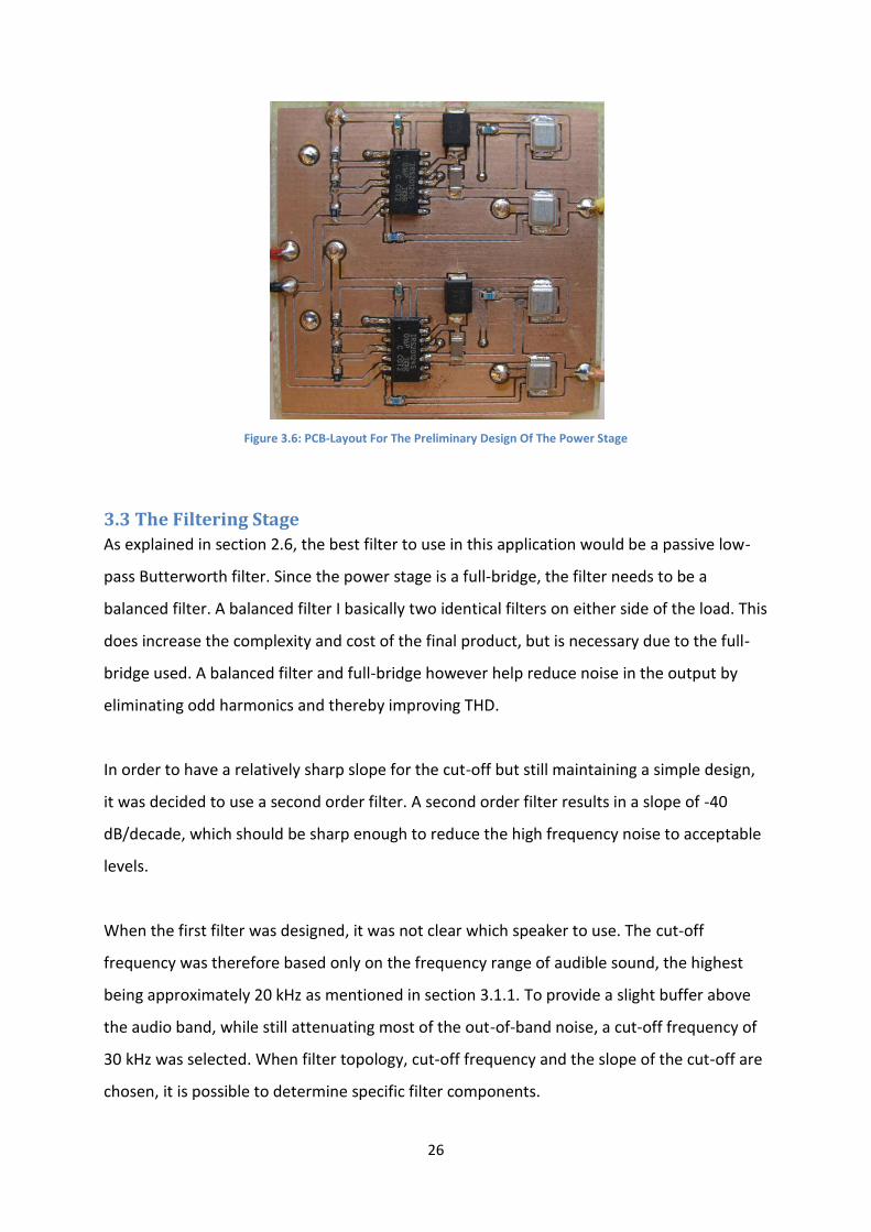
Figure 3.6: PCB-Layout For The Preliminary Design Of The Power Stage
3.3 The Filtering Stage
As explained in section 2.6, the best filter to use in this application would be a passive low-
pass Butterworth filter. Since the power stage is a full-bridge, the filter needs to be a
balanced filter. A balanced filter I basically two identical filters on either side of the load. This
does increase the complexity and cost of the final product, but is necessary due to the full-
bridge used. A balanced filter and full-bridge however help reduce noise in the output by
eliminating odd harmonics and thereby improving THD.
In order to have a relatively sharp slope for the cut-off but still maintaining a simple design,
it was decided to use a second order filter. A second order filter results in a slope of -40
dB/decade, which should be sharp enough to reduce the high frequency noise to acceptable
levels.
When the first filter was designed, it was not clear which speaker to use. The cut-off
frequency was therefore based only on the frequency range of audible sound, the highest
being approximately 20 kHz as mentioned in section 3.1.1. To provide a slight buffer above
the audio band, while still attenuating most of the out-of-band noise, a cut-off frequency of
30 kHz was selected. When filter topology, cut-off frequency and the slope of the cut-off are
chosen, it is possible to determine specific filter components.
27
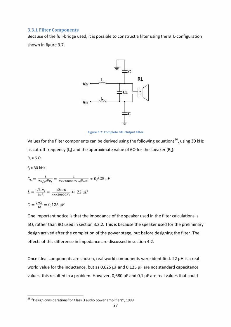
3.3.1 Filter Components
Because of the full-bridge used, it is possible to construct a filter using the BTL-configuration
shown in figure 3.7.
Figure 3.7: Complete BTL Output Filter
Values for the filter components can be derived using the following equations26, using 30 kHz
as cut-off frequency (fc) and the approximate value of 6Ω for the speaker (RL):
RL = 6 Ω
fc = 30 kHz
One important notice is that the impedance of the speaker used in the filter calculations is
6Ω, rather than 8Ω used in section 3.2.2. This is because the speaker used for the preliminary
design arrived after the completion of the power stage, but before designing the filter. The
effects of this difference in impedance are discussed in section 4.2.
Once ideal components are chosen, real world components were identified. 22 µH is a real
world value for the inductance, but as 0,625 µF and 0,125 µF are not standard capacitance
values, this resulted in a problem. However, 0,680 µF and 0,1 µF are real values that could
26 “Design considerations for Class D audio power amplifiers”, 1999.

28
provide an appropriate cut-off frequency. Using the real world values, the frequency of the
cut-off is
It is important that the inductors have low Equivalent Series Resistance (ESR), since they are
in series with the load and all of the power from the amplifier will flow thru them. Since the
capacitors are in parallel with the load, their ESR is of less importance. Components chosen
for the preliminary design were:
Capacitor - Kemet C0805C684K3NACTU (0,680µF)
Capacitor - Avx 08051C104K4T2A (0,1µF)
Inductor - Bourns JW Miller 2305-H-RC (22µH, 7mΩ)
The complete schematic for the filtering stage can be viewed in appendix A.
3.4 Speaker
The initial idea was that the speaker would be selected during the design process of the
preliminary design, but due to limitations in time, this was not possible. Therefore Salvator
HB provided the project-group with a basic horn speaker. Speaker specifications are as
follows:
Model: LBC3491/12
Max power: 15 W
Frequency range: 480 Hz – 5.5 kHz
Sound pressure level at rated output: 118 dB
This speaker was not intended to be used in the final product but merely to function as a
test platform during the build, the reason being really bad sound quality. That is why some
stages, such as the power stage, were not designed with the specifications of this specific
speaker in mind.

29
4 Preliminary Results The following section discusses the results from the preliminary design of the amplifier. This
first step in the design-process was intended as a way of getting to know the class D
amplifier topology. The design was not expected to perform well enough to be considered a
final product, but merely to test one approach for a solution.
4.1 Functionality Testing
4.1.1 The Modulationstage
When testing began with the modulationstage, several design-flaws were discovered. One
problem was that the input audio signal had a small amplitude of about 0.1 V while the
triangle wave had several times larger amplitude, resulting in the comparator saturating.
This was fixed by reducing the ratio R2/R1 on the triangle wave generator, see section 3.1.1.
Another issue was that since the comparator was of the high-speed type, it started
oscillating when the audio-signal and triangle wave had approximately the same amplitude.
This resulted in heavy distortion of the pulses. To avoid this, a slower comparator had to be
used, replacing the TLV3501 with the LM311D. After several tests and fine-tuning of the
modulator, the results were still bad and because of long waiting-times for components to
arrive, it was clear that this circuit would not meet the demands for the final product.
4.1.2 The Power stage
The power stage had to be tested to ensure proper behavior without having the risk of
damaging the speaker. The easiest way of doing this is to apply a positive square wave to
either the high- or low-side and watch the results on the oscilloscope. Both gate drivers and
MOSFETs use the same 12 V supply rail. The power stage was proven to be functional when
an amplified square wave was observed at the output.
Since the modulator was not working as planned, the power stage could not be tested with
the actual modulated signal. Figure 4.1 shows the input square wave and the amplified
output of the power stage, both centered at zero.
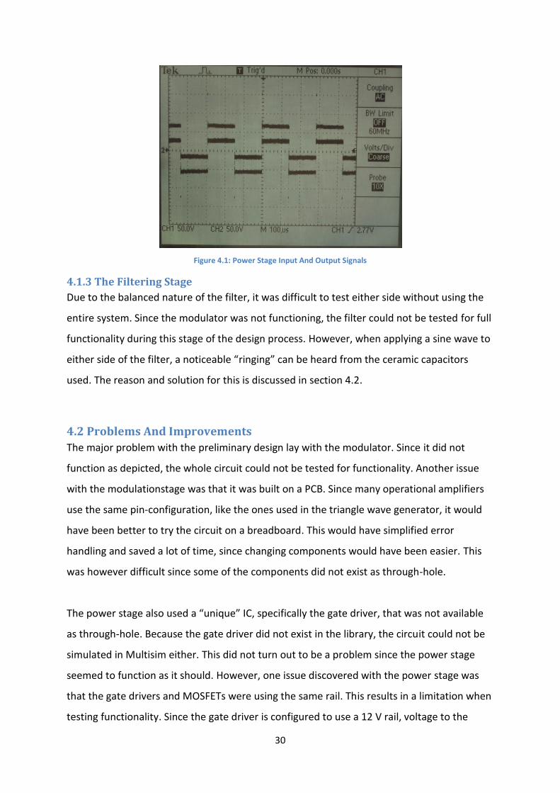
30
Figure 4.1: Power Stage Input And Output Signals
4.1.3 The Filtering Stage
Due to the balanced nature of the filter, it was difficult to test either side without using the
entire system. Since the modulator was not functioning, the filter could not be tested for full
functionality during this stage of the design process. However, when applying a sine wave to
either side of the filter, a noticeable “ringing” can be heard from the ceramic capacitors
used. The reason and solution for this is discussed in section 4.2.
4.2 Problems And Improvements
The major problem with the preliminary design lay with the modulator. Since it did not
function as depicted, the whole circuit could not be tested for functionality. Another issue
with the modulationstage was that it was built on a PCB. Since many operational amplifiers
use the same pin-configuration, like the ones used in the triangle wave generator, it would
have been better to try the circuit on a breadboard. This would have simplified error
handling and saved a lot of time, since changing components would have been easier. This
was however difficult since some of the components did not exist as through-hole.
The power stage also used a “unique” IC, specifically the gate driver, that was not available
as through-hole. Because the gate driver did not exist in the library, the circuit could not be
simulated in Multisim either. This did not turn out to be a problem since the power stage
seemed to function as it should. However, one issue discovered with the power stage was
that the gate drivers and MOSFETs were using the same rail. This results in a limitation when
testing functionality. Since the gate driver is configured to use a 12 V rail, voltage to the

31
MOSFETs could not be increased without having the risk of damaging the gate drivers. This
also ads the possibility that the large drain-current will be affecting the entire circuit at high
output levels. These supply rails needs to be separated in the second revision of the
amplifier.
The power stage also had the drawback of using some “unique” components which were not
present in the library of the CAD software, see section 3.2.4. Since designing new
components was an unfamiliar experience, some design-flaws in the footprints of the
components were discovered during soldering of the PCB. The pads for the gate driver were
quite small, greatly complicating the soldering process. These pads were redesigned for the
second revision.
The filter had an issue with capacitor microphonics, causing the filter-PCB to “sing” when
applying an input signal. This is due to physical movement of the dielectric in the ceramic
capacitors. When operating at a frequency within the audio band and with a signal that has a
high enough amplitude, the effect is audible. This also has the possibility to add distortion to
the output signal. The solution is to change the ceramic capacitors, see figure 4.2, to film-
capacitors for the second filter-revision.
Figure 4.2: Ceramic Capacitors Causing The ”Singing”
The preliminary design also suffered from a difference in speaker impedance-matching. The
power stage used 8Ω when calculating peak voltage and drain current. The filter however
used 6Ω when calculating cut-off frequency. The difference was due to a late arrival of the
speaker, when the power stage was already soldered. The effect of this disparity is that it
would take more power to drive the speaker than the calculations in section 3.2.2 originally
suggested. This did not turn out to be a big problem since changes in the design was to be
made for the improved version of the amplifier.
32
5 Improved Design And Construction The preliminary design had a few flaws that were discussed in section 4.2. These were all
addressed and corrected for the second revision of the amplifier. The major change involved
a completely new approach to the modulationstage and a new speaker that could be used in
the final product. The following section outlines the changes in each stage. As with the
preliminary design, components were chosen to match the temperature requirement
specified in table 1.
5.1 Changing Speaker
The improved design would have to feature a new speaker so that extensive testing could be
conducted. The speaker used must be able to output 106dB as stated in section 2.7. A good
option was the DSP3012A which provided a maximum output of 131dB. This particular
speaker however had a slightly different IP-classification, namely IP56. This means that the
dust-protection was not as good but protection against water is better, compared to IP65. It
was decided, in coordination with Salvator HB, that this classification would still be sufficient
for the purpose of this project. Full specifications for the speaker can be seen in appendix D.
As the new speaker probably would be used in the final product, the amplifier could be
designed to match all specifications.
5.2 The Modulationstage
When constructing the new modulationstage, it was important to find a solution that was
tried and working. Simplicity in design was important to be able to quickly determine if the
new solution would be feasible or not. Also, a simple design often requires the use of fewer
active components, which in turn drains less power.
5.2.1 Self-Oscillating Modulator
A not so widely used method in class D amplifiers is self-oscillating modulation. As described
in section 2.3.3, the modulator works by using a feedback-loop to determine the switching
frequency. With this type of modulation it is possible to achieve high-quality audio with few
components. Since the only drawback is difficulties when synchronizing with other switching
devices and no such synchronization is needed in this project, self-oscillating modulation
could provide a feasible solution.
33
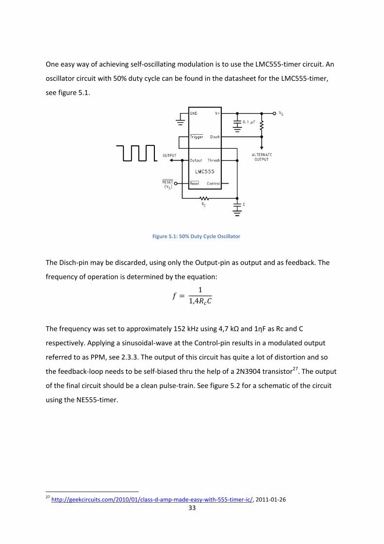
One easy way of achieving self-oscillating modulation is to use the LMC555-timer circuit. An
oscillator circuit with 50% duty cycle can be found in the datasheet for the LMC555-timer,
see figure 5.1.
The Disch-pin may be discarded, using only the Output-pin as output and as feedback. The
frequency of operation is determined by the equation:
The frequency was set to approximately 152 kHz using 4,7 kΩ and 1ηF as Rc and C
respectively. Applying a sinusoidal-wave at the Control-pin results in a modulated output
referred to as PPM, see 2.3.3. The output of this circuit has quite a lot of distortion and so
the feedback-loop needs to be self-biased thru the help of a 2N3904 transistor27. The output
of the final circuit should be a clean pulse-train. See figure 5.2 for a schematic of the circuit
using the NE555-timer.
27
http://geekcircuits.com/2010/01/class-d-amp-made-easy-with-555-timer-ic/, 2011-01-26
Figure 5.1: 50% Duty Cycle Oscillator
34
In order to be able to use this circuit in the project, some changes to the schematic had to be
made. 12 V instead of 5 V is used, changes in resistor-values are needed for correct DC-offset
adjustments at the CV pin and the LMC555-timer was used instead of the NE555. This is
because the LMC555 requires lower supply current, is capable of operating at a higher
frequency and has lower power dissipation.
In order to provide the full-bridge used as power stage with low- and high-side signals, the
output of the modulator needs to be split in half and converted to positive pulses only. This
is easily achieved by using a standard logic XOR-gate (CD4030)28. The XOR-gate acts as a
phase splitter, effectively dividing the modulated AC-signal into high- and low-side, see
figure 5.3, low being the same as the high-side but with inverted pulses.
28
http://geekcircuits.com/2010/02/full-bridge-class-d-amp-using-555-timer/, 2011-01-27
Figure 5.3: XOR-Gate Acting As A Phase Splitter
Figure 5.2: Self-Oscillating Modulator Using NE555 With Negative Feedback27
35
Let us take the high-side as an example. Input signals with negative voltage are compared to
Vcc on the second input of the XOR-gate, resulting in a positive output. The result becomes
more evident when looking at the truth table of the XOR-gate, see table 4. The low-side uses
GND as reference instead of Vcc and thus provides a positive output when the input signal is
positive.
Table 4: Truth Table Of High-Side XOR-Gates
5.2.2 Breadboard- And PCB Layout
The new version of the modulator was possible to construct on a breadboard, in order to
simplify error handling and test the functionality of the circuit. It was assumed that the
output of the modulator on the breadboard would be fairly noisy, but since this step was
only to ensure proper behavior, noise was accepted.
Once the functionality of the breadboard modulator was confirmed, a PCB was
manufactured and all components soldered into place. Figure 5.4 and 5.5 shows the
evolution of the modulator from breadboard to PCB. The full schematic for the
modulationstage can be viewed in appendix E.
Figure 5.4: Breadboard Modulator
Input
Vcc In
Output
high-side
1 0 1
1 1 0
36
Figure 5.5: PCB-Layout Of The Modulator
5.3 The Power stage
The power stage from the preliminary design was proven functional in regards to amplifying
a square wave. However, as discussed in section 4.2, the power stage had some major flaws
that needed to be corrected for the improved design.
The first issue to be solved was to separate the supply for the gate driver and the MOSFETs.
This was easily done in the CAD-software. Also the pads for the gate drivers were redesigned
to simplify soldering. The second issue was the mismatch of speaker impedance described in
section 4.2. The speaker used in the improved version however had an impedance of 8Ω,
thus not requiring any changes in the power stage due to the change of speaker. The PCB for
the improved version of the power stage can be seen in figure 5.6. The full schematic for the
power stage can be viewed in appendix E.
Figure 5.6: PCB-Layout, Improved Version Of The Power Stage

37
5.4 The Filtering Stage
The filter needed different capacitors to avoid the “ringing” described in section 4.2. The
solution was to use film-capacitors as these are better suited for audio purposes29. With the
new and “final” speaker selected, it was also possible to match the cut-off to the impedance
and frequency range of the speaker.
Since the speaker had an upper limit of 18 kHz, it was decided that the cut-off frequency
could be lowered to further filter out unwanted noise. Using the equations in 3.3.1 and the
new values of 1,5µF and 0,3µF for the capacitors, the cut-off frequency is approximately
19590 Hz. The PCB for the improved filtering stage can be seen in figure 5.7. The full
schematic for the filtering stage can be viewed in appendix E.
Figure 5.7: Improved Version Of The Filtering Stage
6 Improved Version Results Once all parts of the improved version were constructed, it was possible to test the entire
amplifier for functionality. Listening tests as well as sound pressure measurements were
conducted to ensure proper behavior.
6.1 Functionality Testing
6.1.1 The Modulationstage
Initial testing with the modulator involved just connecting the supply-rails and looking at the
output without any input signal to modulate. The results were identical pulses on both the
29
http://www.audiocaps.com/, 2011-03-02

38
high- and low-sides of the XOR-gate, see figure 6.1. The pulses were not entirely clean, but
was assumed to be good enough to be able to use when testing the full system.
Figure 6.1: Modulator Output (High-Side), No Input Signal
The next step was to apply a sine wave to the CV-pin to see if the result was a modulated
output. The modulationstage was confirmed to be functional when a modulated output was
observed at both the low- and high-side of the XOR-gate, see figure 6.2 and figure 6.3.
Figure 6.2: Modulated Output, Low-Side

39
Figure 6.3: Modulated Output, High-Side
6.1.2 The Power stage
The improved version of the power stage was tested the same way as the preliminary
design, by applying a square wave to both the high- and low-side of the gate driver. The
results can be viewed in figure 6.4.
Figure 6.4: Power Stage Input And Output Signals

40
6.1.3 The Filtering Stage
With the new film-capacitors, the issue with microphonics described in section 4.2 was
solved. Since the filter still was of the balanced type, testing would be easier to conduct
using the modulator. The modulator was connected to the filter and a sine wave was used as
input. The results using a 10 kHz and 20 kHz sine wave is showed in figure 6.5 and figure 6.6
respectively. At 20 kHz, the amplitude of the sine wave has dropped about -3 dB and thereby
verifies the calculated cut-off frequency of approximately 19590 Hz.
Figure 6.6: Filter Output Using A 20 kHz Sine Wave
Figure 6.5: Filter Output Using A 10 kHz Sine Wave
41
6.1.4 Full system Assembly
Since all stages were working for the improved version of the amplifier, it was possible to
assemble the entire circuit and conduct testing with sound as input. The tests used a large
CD-player as source to get a high quality audio signal.
Each stage uses one or two power supplies depending on needs. This was to see if different
supply voltages had different effects on the entire amplifier, so that correct voltage
regulators could be picked out for a final circuit.
6.2 Speaker Testing
The following section outlines some tests done with the speaker connected directly to the
CD-player and to the class D amplifier constructed in this project. The CD-player acted as a
reference for audio quality as well as allowing measurements of the maximum sound-
pressure the speaker would be able to produce.
6.2.1 Listening Test
Listening tests are quite subjective and could vary a lot between each tester. Therefore,
listening tests were conducted using both the CD-player and the class D amplifier. Using two
different amplifiers allowed for a reference so that the quality of the audio from the class D
amplifier could be compared to the "clean" audio from the CD-player. Various sounds such
as high quality music, gunshots, explosions etc, were listened to at different volumes by
several people.
One thing became very clear when listening to the audio from the class D amplifier. At low
volumes (small input signal), the sound was very good. Everything from music to gunshots
could be heard with very little distortion. As the volume was increased however, distortion
became more and more prominent finally resulting in a very bad “crackling”- noise at high
volumes. Possible reasons for this noise are discussed in section 7.
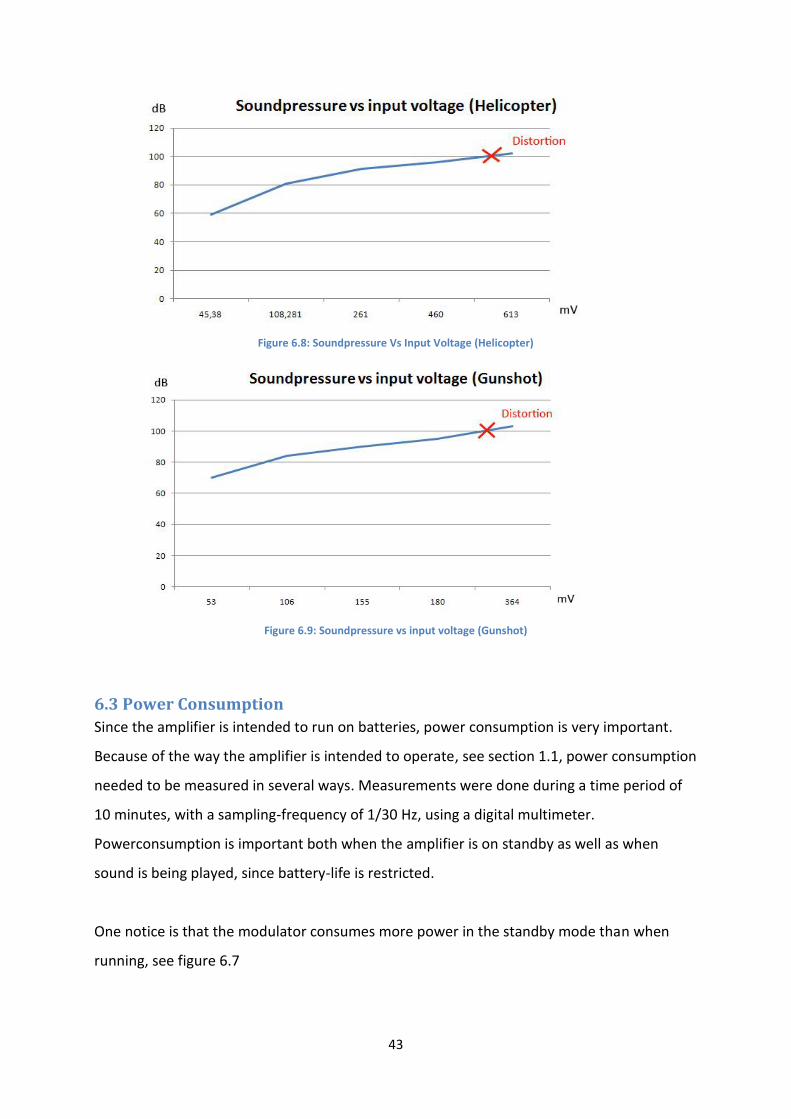
6.2.2 Soundpressure
Soundpressure was measured using a Velleman AVM2050 analogue sound level meter. The
sound pressure was measured while increasing the amplitude of the input signal until the
desired output soundpressure of 106 dB was achieved. Three different sounds were used for
measuring; a part of a music track, helicopter sound and gunshot sound. The speaker was
42
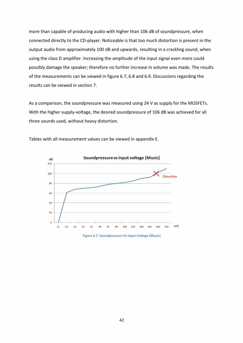
more than capable of producing audio with higher than 106 dB of soundpressure, when
connected directly to the CD-player. Noticeable is that too much distortion is present in the
output audio from approximately 100 dB and upwards, resulting in a crackling sound, when
using the class D amplifier. Increasing the amplitude of the input signal even more could
possibly damage the speaker; therefore no further increase in volume was made. The results
of the measurements can be viewed in figure 6.7, 6.8 and 6.9. Discussions regarding the
results can be viewed in section 7.
As a comparison, the soundpressure was measured using 24 V as supply for the MOSFETs.
With the higher supply-voltage, the desired soundpressure of 106 dB was achieved for all
three sounds used, without heavy distortion.
Tables with all measurement values can be viewed in appendix E.
Figure 6.7: Soundpressure Vs Input Voltage (Music)
43
Figure 6.8: Soundpressure Vs Input Voltage (Helicopter)
Figure 6.9: Soundpressure vs input voltage (Gunshot)
6.3 Power Consumption
Since the amplifier is intended to run on batteries, power consumption is very important.
Because of the way the amplifier is intended to operate, see section 1.1, power consumption
needed to be measured in several ways. Measurements were done during a time period of
10 minutes, with a sampling-frequency of 1/30 Hz, using a digital multimeter.
Powerconsumption is important both when the amplifier is on standby as well as when
sound is being played, since battery-life is restricted.
One notice is that the modulator consumes more power in the standby mode than when
running, see figure 6.7

44
Figure 6.10: Powerconsumption, Modulator
Figure 6.11: Powerconsumption, Power Stage In Standby
As seen in figure 6.11, the powerconsumption for the power stage is quite low. It only
slightly increases over time, which could be the result of a temperature increase in the
circuits. However, the difference in supply-current between startup and after 10 minutes is
only 0,226 mA, which is easily negligible.
Measuring the powerconsumption of the power stage when it is running is difficult, due to
large current-fluctuations depending on the type of sound being played. However, the
largest noticeable value when trying to measure was something around 85 mA (for music),

45
which is only a minor increase from standby-current. The largest value for the current for the
entire circuit would then be;
This would result in a runtime of approximately 50 hours, using one 5 Ah battery. A table
with all the measurement values can be viewed in appendix F.
7 Problems With The Improved Version The improved version of the amplifier incorporated a series of changes from the preliminary
design. A completely new modulator was constructed and implemented, the power stage
required some small changes and the filter was redesigned for increased functionality. This
section outlines the problems with the improved design. Some possible solutions to these
problems are discussed in section 9.
Problems with the improved version consist mainly of distortion in the output audio at high
volumes. There could be several reasons for this. The main problem is the limited supply-
voltage of 12 V. This greatly limits the voltage swing of the modulator, allowing for a rather
small input signal to be handled and also limiting the amplitude of the output from the
modulator. Increasing the supply-voltage also increases the total amplification, as discussed
briefly in section 6.2.2. With a supply of 24 V, the desired soundpressure of 106 dB was
achieved with very little distortion in the output audio. But with only 12 V, the maximum
soundpressure was approximately 100 dB and even then, a lot of distortion could be heard.
Another issue is the modulator itself. The self-oscillating modulator used in this project is not
designed to produce high-quality audio, especially not at extremely high volumes; therefore
distortion is inevitable as some point. A possible problem is the feedback of the modulator.
Large input signals result in a lot of variation in the position of the pulses in the output. This
could possibly push the feedback transistor out of its linear region, resulting in distortion.
Adjusting the modulation frequency could also help reduce noise in the output.
One issue discovered with the power stage was that when the rails for the MOSFETS and the
gate drivers were separated, the MOSFETs did not have any dedicated bypass capacitors.
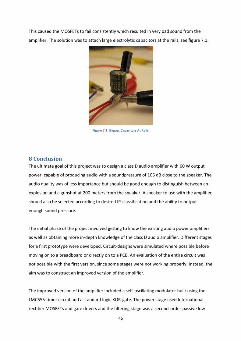
46
This caused the MOSFETs to fail consistently which resulted in very bad sound from the
amplifier. The solution was to attach large electrolytic capacitors at the rails, see figure 7.1.
Figure 7.1: Bypass Capacitors At Rails
8 Conclusion The ultimate goal of this project was to design a class D audio amplifier with 60 W output
power, capable of producing audio with a soundpressure of 106 dB close to the speaker. The
audio quality was of less importance but should be good enough to distinguish between an
explosion and a gunshot at 200 meters from the speaker. A speaker to use with the amplifier
should also be selected according to desired IP-classification and the ability to output
enough sound pressure.
The initial phase of the project involved getting to know the existing audio power amplifiers
as well as obtaining more in-depth knowledge of the class D audio amplifier. Different stages
for a first prototype were developed. Circuit-designs were simulated where possible before
moving on to a breadboard or directly on to a PCB. An evaluation of the entire circuit was
not possible with the first version, since some stages were not working properly. Instead, the
aim was to construct an improved version of the amplifier.
The improved version of the amplifier included a self-oscillating modulator built using the
LMC555-timer circuit and a standard logic XOR-gate. The power stage used International
rectifier MOSFETs and gate drivers and the filtering stage was a second-order passive low-
47
pass Butterworth filter with large toroidal inductors and film-capacitors. An appropriate
speaker was also selected for the improved version. The speaker is able to output a
maximum of 131 dB which is well above the desired 106 dB required for this project. The
IP56-classification on the speaker also met the demands.
Listening tests, as well as sound pressure measurements were conducted on the improved
version of the amplifier. The listening tests showed that the amplifier was able to produce
“good” quality audio at low volumes, but had a lot of distortion when the volume was
increased. The desired soundpressure of 106 dB was not achieved during tests with 12 V as
supply; instead the maximum soundpressure without heavy distortion is approximately 100
dB. The project specification regarding soundpressure was however met when increasing the
supply voltage to at least 24 V, i.e. using two batteries.
Powerconsumption was also of major importance and specifications were met, with almost
51 hours of runtime using the current setup. Changes in amplifier-design, such as
redesigning the modulator or construct the entire circuit on one PCB, will however affect
powerconsumption and further calculations are needed before making these changes. This
however shows the major advantage that class D has towards regular class AB amplifiers in
regards to efficiency.
Connectors and volume-control were not implemented because some parts of the amplifier
may be changed for the final product.
Although not meeting all the criteria for a finished product, the improved version of the class
D amplifier still was a major step towards that goal. Some errors were expected while others
showed up during the design-process. Improvements can be made, as with any design, to
achieve the best possible results given the current project specifications. But due to the
narrow time frame, these further improvements were beyond the scope of this project.

48
9 Improvements And Future Work Although an almost working prototype, the amplifier still has a long way to go before it
would be considered a finished product. In the following sections, several possible
improvements are discussed for the different stages of the amplifier.
9.1 The Modulation stage
The modulator proved to be a working design in regards to successfully modulating the input
audio into pulses. However, several restrictions were discovered during testing of the
improved version of the amplifier.
First off, there are a few improvements that can be made to the existing modulator. One
possible way of reducing distortion would be to adjust resistor values for appropriate
feedback at high volumes, as discussed in section 7. The modulation frequency could also be
adjusted to further optimize noise handling. This is not guaranteed to work however and the
current modulator is still restricted to the 12 V supply.
Another alternative would be to investigate whether or not the second battery mentioned in
section 1.1 could be used to create a dual supply. This would increase the number of
possible designs to use for the modulator and also increase the headroom for the input
signal. If a complete change of modulation technique is needed, the dual supply would allow
the implementation of a sigma-delta modulator, which could yield several advantages:
Superior noise handling due to several feedback-paths in higher-order sigma-delta
modulators
Increased headroom for the input signal due to the dual power-supply used
The high modulation frequency used in sigma-delta modulators pushes noise further
out of the audio-band and increases the overall efficiency of the amplifier
Using a sigma-delta modulator would also broaden the area of use, making the amplifier
suitable for applications where high-quality audio is needed.
9.2 The Power Stage
The power stage was proven to be functional in the improved version of the amplifier. The
major improvement needed is dedicated bypass capacitors at the rails in order to have a
correct functionality of the MOSFETs. Dead time could also be adjusted for increased
efficiency, but this is dependent on the modulation technique used.
49
9.3 The Filtering Stage
The filter used for the improved version of the amplifier has a cut-off frequency that is quite
low. This is because of the type of speaker used, which only handles frequencies up to
18 000 Hz and also because of the rather low modulation frequency. The low cut-off does
however affect the audible sound so that high-frequencies get attenuated. This will color the
listening experience in a negative way, resulting in a sound picture that is less dynamic than
would be optimal. Should however the modulation technique change so that a higher
modulation frequency could be used, it would be possible to increase the cut-off to obtain
better sound-quality.
Another improvement would be to use inductors that have a lower resistance. This change
increases the efficiency of the filter.
9.4 Pre-amplification Stage
When doing tests with the amplifier, the input of the modulator was connected to the
headphone output of a CD-player. In this way, it was possible to adjust the amplitude of the
input signal simply by adjusting the volume on the CD-player. This will however not be
possible in the final product, where the likely audio source will be a low-power MP3-player;
thus demanding the use of a pre-amplifier. It would also be possible to implement volume
control in the pre-amplification stage, by using a simple potentiometer to limit the input
signal.
There are several ways of constructing a pre-amplifier. Transistor-based versions are widely
used where the input signal is very small, i.e. as microphone pre-amps. These generally only
need a single supply, but with the downside of easily being overdriven when increasing the
input signal. Another alternative would be to use a ready-made pre-amp, based on
operational amplifiers designed specifically for audio purposes. These however often require
the use of a dual power-supply, but benefits from the ability to handle larger variations in
amplitude of the input audio.
50
Both designs have their benefits and downsides, but in order to select the appropriate
design, further research is needed.
9.5 General Improvements
Although each stage of the amplifier needs specific improvements, there are several issues
that need to be addressed regarding the entire circuit.
The current version of the amplifier is tied to the lab-bench since several different power-
supplies are used. In order to have a finished product, each stage will need dedicated
voltage regulators and line protection so that the large current-fluctuations caused by the
MOSFETs do not affect the other stages.
The finished amplifier will also have to be constructed on a single PCB. This will possibly
reduce noise currently caused by the cables connecting the stages to each other. Error
handling is however complicated when using one single PCB, therefore each stage must be
finalized before progressing further.
51
References
http://www.physicsclassroom.com/class/sound/u11l2b.cfm, 2011-02-03
Boylestad, ”Introductory Circuit Analysis”, Tenth Edition, 1996, page 701
http://en.wikipedia.org/wiki/Electronic_amplifier, 2010-10-03
http://sound.westhost.com/articles/pwm.htm, 2010-10-06
http://www.irf.com/whats-new/nr071002.html, 2010-10-06
Briana, M. “Class D Audio Amplifier: the design of a live audio Class D audio amplifier with greater
than 90% efficiency and less than 1% distortion”, 2008
http://www.eetimes.com/design/audio-design/4015790/Class-D-Audio-Amplifiers-What-Why-and-
How--Part-5, 2010-10-06
Nielsen, K., "A Review and Comparison of Pulse-Width Modulation (PWM) Methods for Analog and
Digital Input Switching Power Amplifiers”, 1997
http://www.eetimes.com/design/audio-design/4015790/Class-D-Audio-Amplifiers-What-Why-and-
How--Part-5?pageNumber=0, 2010-10-06
http://en.wikipedia.org/wiki/Sliding_mode_control, 2010-10-15
http://www.argospress.com/Resources/CommunicationsSystems/pulpositimodula.htm, 2011-01-26
www.irf.com/technical-info/appnotes/an-1071.pdf, 2011-01-28
http://www.eetimes.com/design/audio-design/4015895/Class-D-amplifier-FAQ--Part-1-Overview-
amplifier-selection-and-filters?pageNumber=2, 2010-10-15
Kerry, L., “A Basic Introduction to Filter-- Active, Passive, and Switched-Capacitor”, 1991
http://www.eetimes.com/design/audio-design/4015847/Understanding-output-filters-for-Class-D-
amplifiers, 2010-10-28
http://www.electronics-tutorials.ws/filter/filter_2.html, 2010-11-26
http://i.cmpnet.com/audiodesignline/2006/05/TIFig3.JPG, 2011-02-03
http://en.wikipedia.org/wiki/Horn_loudspeaker, 2011-02-28
http://www.play-hookey.com/analog/images/square_triangle_gen.gif, 2011-01-25
http://www.play-hookey.com/analog/triangle_waveform_generator.html, 2011-01-25
http://en.wikipedia.org/wiki/Nyquist_rate, 2011-01-25
http://hyperphysics.phy-astr.gsu.edu/hbase/sound/earsens.html, 2011-01-25
http://www.swarthmore.edu/NatSci/echeeve1/Ref/SingleSupply/SingleSupply.html, 2011-01-25
“Design considerations for Class D audio power amplifiers”, 1999.
http://geekcircuits.com/2010/01/class-d-amp-made-easy-with-555-timer-ic/, 2011-01-26
http://geekcircuits.com/2010/02/full-bridge-class-d-amp-using-555-timer/, 2011-01-27
http://www.audiocaps.com/, 2011-03-02

52
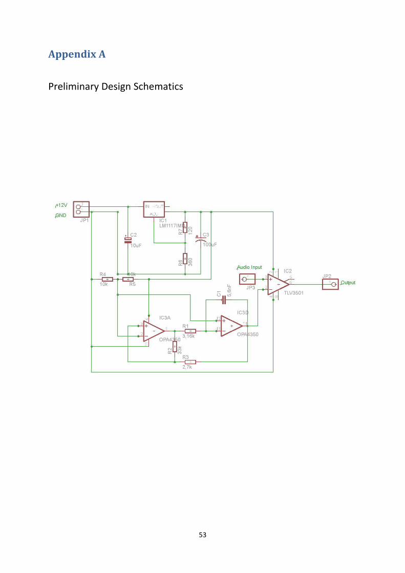
53
Appendix A
Preliminary Design Schematics

54

55
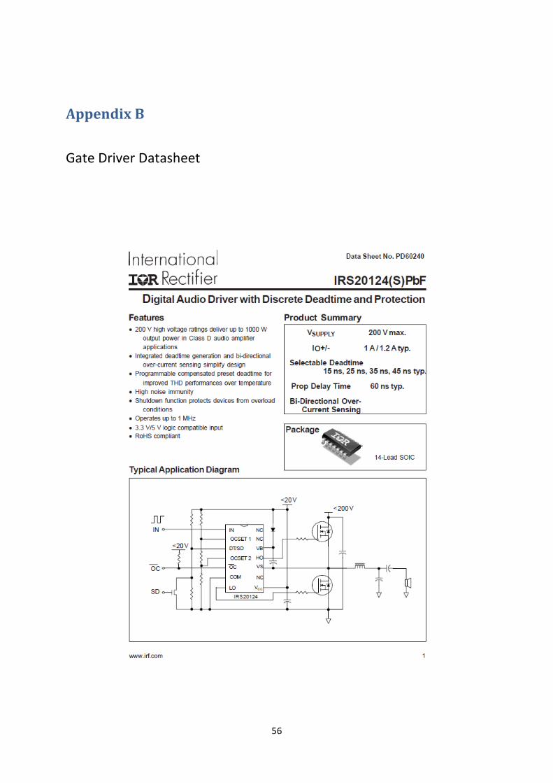
56
Appendix B
Gate Driver Datasheet

57

58
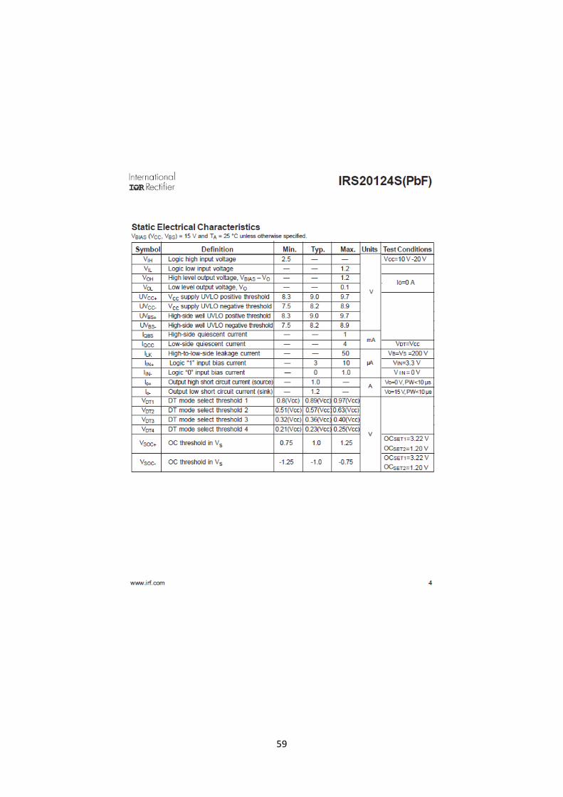
59
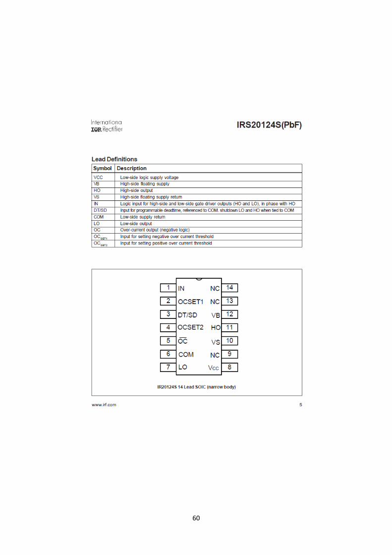
60

61
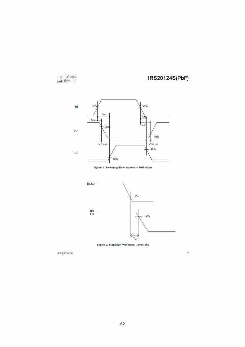
62

63
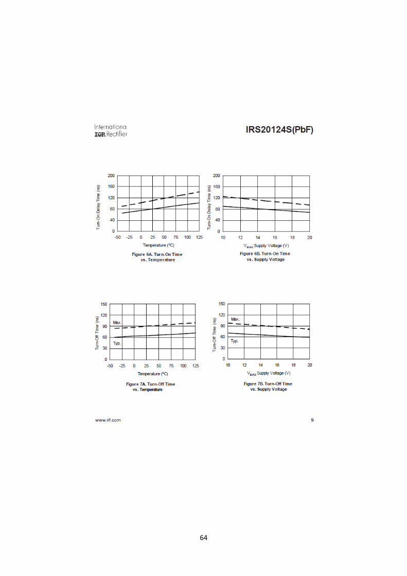
64

65
66
67

68

69
70
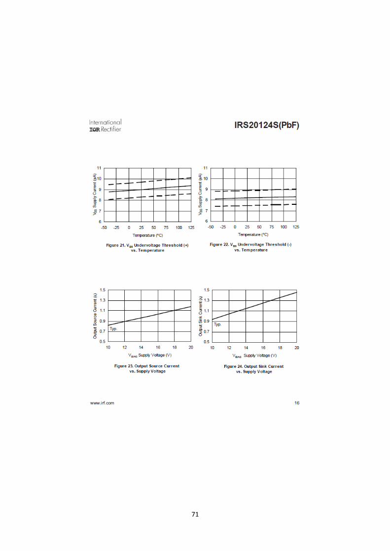
71
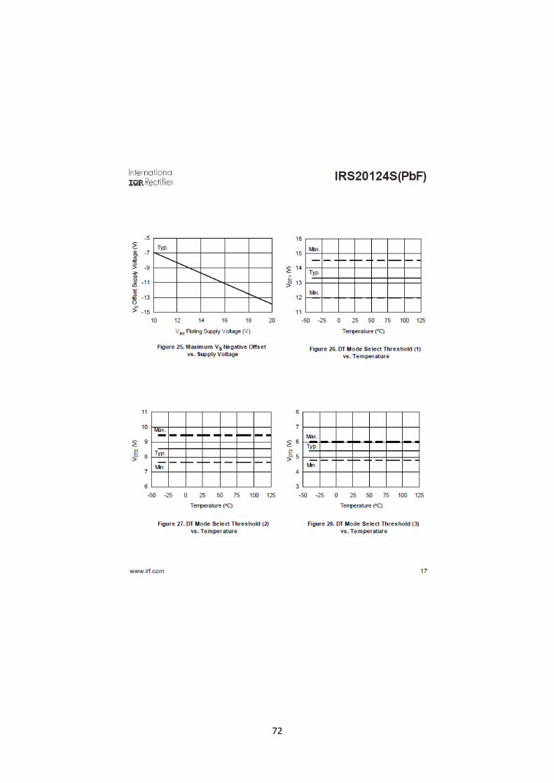
72

73
74

75
76

77

78
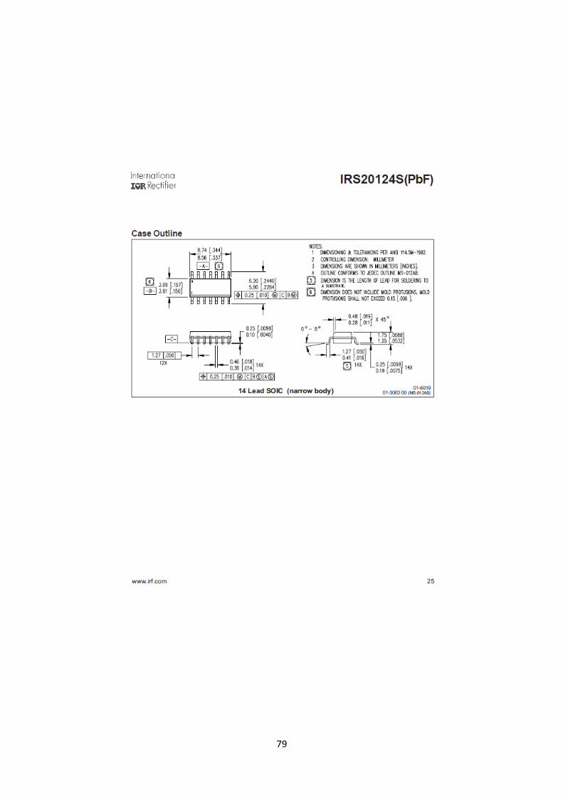
79

80

81

82
Appendix C
MOSFET Datasheet
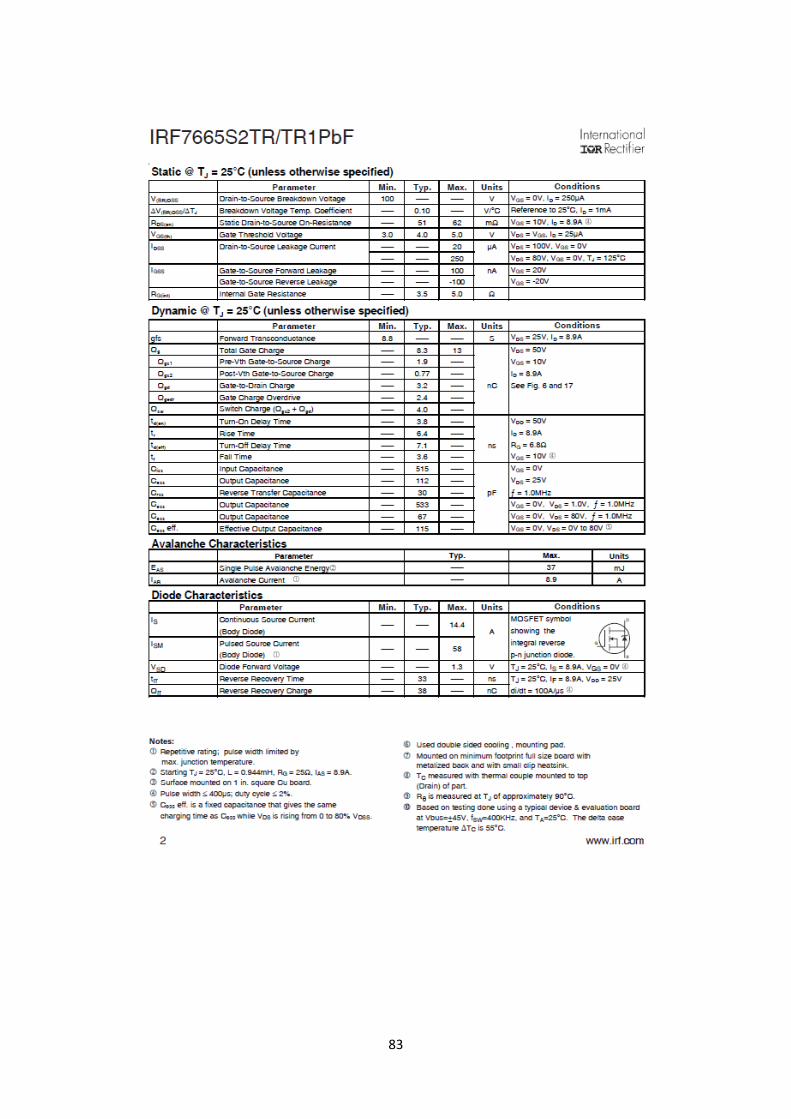
83

84
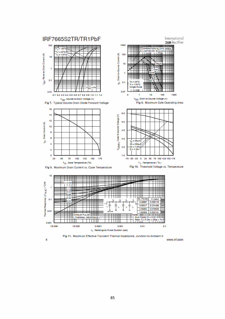
85

86
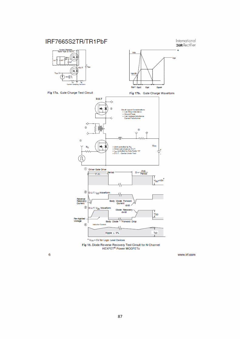
87

88

89
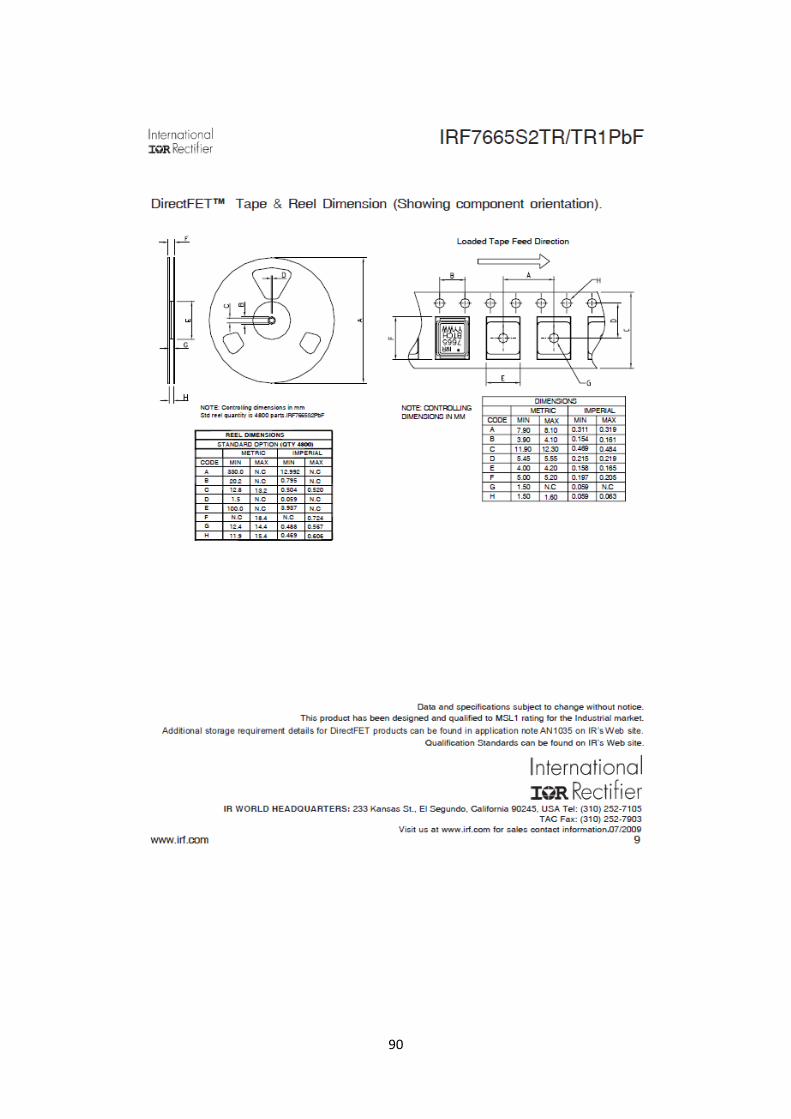
90
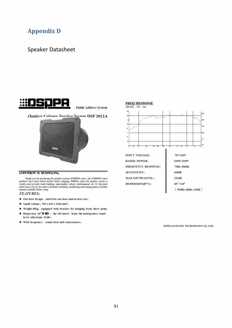
91
Appendix D
Speaker Datasheet

92
Appendix E
Improved Version Schematics
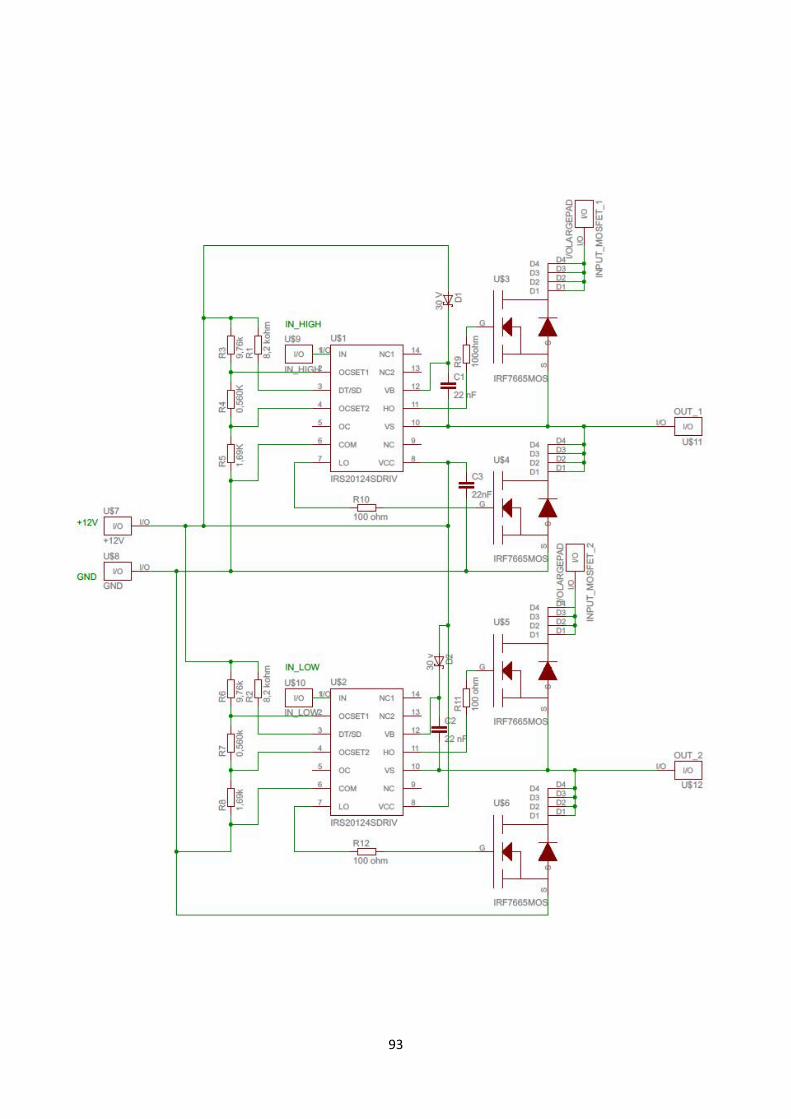
93
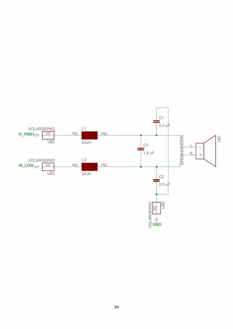
94

95
Appendix F
Soundpressure Measurements
Soundpressure vs input voltage (Music)
Vin (mV) pSPL (dB)
15 0
20 61
25 68
30 70
35 71
40 74
45 78
80 80
100 82
150 85
200 90
350 92
600 102
700 110
Soundpressure vs input voltage (Helicopter)
Vin (mV) pSPL (dB)
45,38 59
108,281 81
261 91
460 96
613 102
Soundpressure vs input voltage (Gunshot)
Vin (mV) pSPL (dB)
53 70
106 84
155 90
180 95
364 103
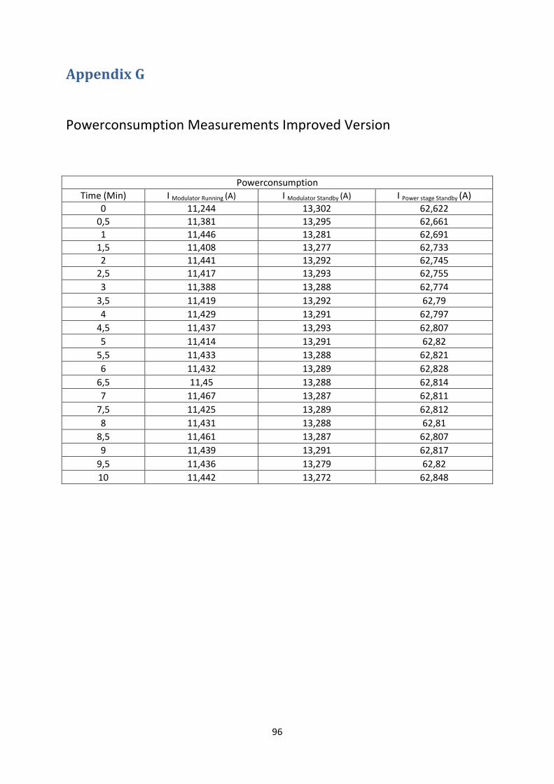
96
Appendix G
Powerconsumption Measurements Improved Version
Powerconsumption
Time (Min) I Modulator Running (A) I Modulator Standby (A) I Power stage Standby (A)
0 11,244 13,302 62,622
0,5 11,381 13,295 62,661
1 11,446 13,281 62,691
1,5 11,408 13,277 62,733
2 11,441 13,292 62,745
2,5 11,417 13,293 62,755
3 11,388 13,288 62,774
3,5 11,419 13,292 62,79
4 11,429 13,291 62,797
4,5 11,437 13,293 62,807
5 11,414 13,291 62,82
5,5 11,433 13,288 62,821
6 11,432 13,289 62,828
6,5 11,45 13,288 62,814
7 11,467 13,287 62,811
7,5 11,425 13,289 62,812
8 11,431 13,288 62,81
8,5 11,461 13,287 62,807
9 11,439 13,291 62,817
9,5 11,436 13,279 62,82
10 11,442 13,272 62,848


