
CORP IR / May 29, 2018 1
May 29, 2018
Toshiki Kawai
Representative Director, President & CEO
Medium-term Management Plan Progress and
New Financial Model

CORP IR / May 29, 2018 2
Disclaimer regarding forward-looking statement
Forecast of TEL’s performance and future prospects and other sort of information published are made based on information
available at the time of publication. Actual performance and results may differ significantly from the forecast described here due to
changes in various external and internal factors, including the economic situation, semiconductor/FPD market conditions,
intensification of sales competition, safety and product quality management, and intellectual property-related risks.
Processing of numbers
For the amount listed, because fractions are rounded down, there may be the cases where the total for certain account titles does
not correspond to the sum of the respective figures for account titles. Percentages are calculated using full amounts, before
rounding.
Exchange risk
In principle, export sales of Tokyo Electron’s mainstay semiconductor and FPD production equipment are denominated in yen.
While some settlements are denominated in dollars, exchange risk is hedged as forward exchange contracts are made individually
at the time of booking. Accordingly, the effect of exchange rates on profits is negligible.
Disclaimer regarding IHS Markit data (Page 92, 95, 97)The IHS Markit reports and information referenced herein (the "IHS Markit Materials") are the copyrighted property of IHS Markit Ltd. (“IHS Markit”) and represent data, research, opinions or
viewpoints published by IHS Markit, and are not representations of fact. The IHS Markit Materials speak as of the original publication date thereof (and not as of the date of this offering
document). The information and opinions expressed in the IHS Markit Materials are subject to change without notice and IHS Markit has no duty or responsibility to update the IHS Markit
Materials. Moreover, while the IHS Markit Materials reproduced herein are from sources considered reliable, the accuracy and completeness thereof are not warranted, nor are the opinions
and analyses which are based upon it. To the extent permitted by law, IHS Markit shall not be liable for any errors or omissions or any loss, damage or expense incurred by reliance on the
IHS Markit Materials or any statement contained herein, or resulting from any omission. No portion of the IHS Markit Materials may be reproduced, reused, or otherwise distributed in any
form without the prior written consent of IHS Markit. Content reproduced or redistributed with IHS Markit’s permission must display IHS Markit’s legal notices and attributions of authorship.
IHS Markit and the IHS Markit globe design are trademarks of IHS Markit. Other trademarks appearing in the IHS Markit Materials are the property of IHS Markit or their respective owners.
Disclaimer regarding Gartner data (Page 53, 54, 84)All statements in this presentation attributable to Gartner represent Tokyo Electron’s interpretation of data, research opinion or viewpoints published as part of a syndicated subscription
service by Gartner, Inc., and have not been reviewed by Gartner. Each Gartner publication speaks as of its original publication date (and not as of the date of this presentation). The opinions
expressed in Gartner publications are not representations of fact, and are subject to change without notice.
FPD: Flat panel display
Forward Looking Statements
CORP IR / May 29, 2018 3
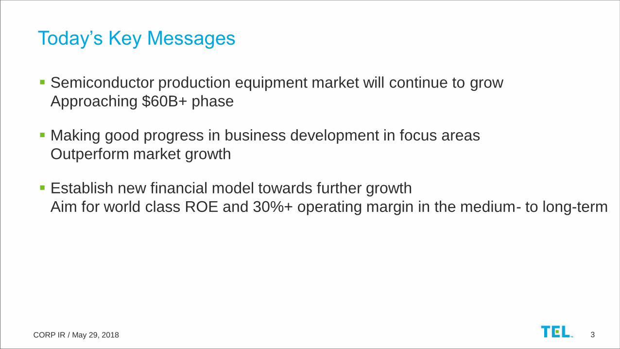
Semiconductor production equipment market will continue to grow
Approaching $60B+ phase
Making good progress in business development in focus areas
Outperform market growth
Establish new financial model towards further growth
Aim for world class ROE and 30%+ operating margin in the medium- to long-term
Today’s Key Messages

CORP IR / May 29, 2018 4
FY2018 (April 2017-March 2018) Highlights
Net sales +41% YoY driven by the growth of the SPE* and FPD** market and expansion of market share in focus areas
Operating income and net income attributable to owners of parent reached new record highs
Net Sales and Gross Profit Margin
612.1 613.1 663.9
799.7
33.0%
39.6% 40.2% 40.3%42.0%
0
400
800
1,200
FY'14 FY'15 FY'16 FY'17 FY'18
Net sales (¥B)
Gross profit margin
32.2
88.1116.7
155.6
281.1
5.3%
14.4%
17.6%19.5%
24.9%
0.0%
5.0%
10.0%
15.0%
20.0%
25.0%
30.0%
0
100
200
300
FY'14 FY'15 FY'16 FY'17 FY'18
Operating income (¥B)
Operating margin
Operating Income and Operating Margin
Net Income Attributable to
Owners of Parent and ROE
1,130.7
-19.4
71.8 77.8
115.2
204.3
-3.3%
11.8%13.0%
19.1%
29.0%
-20
80
180
FY'14 FY'15 FY'16 FY'17 FY'18
Net income attributable toowners of parent (¥B)
ROE
* SPE: Semiconductor production equipment
** FPD: Flat panel display

CORP IR / May 29, 2018 5
(Billion yen)
FY2018
(Actual)
FY2019 (Estimates)
H1 H2 Full yearFull year
YoY change
Net sales 1,130.7 690.0 710.0 1,400.0 +23.8%
SPE 1,055.2 634.0 654.0 1,288.0 +22.1%
FPD 75.0 56.0 56.0 112.0 +49.2%
Gross profitGross profit margin
475.042.0%
288.041.7%
310.043.7%
598.042.7%
+122.9+0.7pts
SG&A expenses 193.8 115.0 117.0 232.0 +38.1
Operating incomeOperating margin
281.124.9%
173.025.1%
193.027.2%
366.026.1%
+84.8+1.2pts
Income before income taxes 275.2 173.0 193.0 366.0 +90.7
Net income attributable to
owners of parent204.3 128.0 142.0 270.0 +65.6
Net income per share (Yen) 1,245.48 779.95 - 1,645.20 +399.72
FY2019 Financial Estimates
Expect to generate record high profits* for third consecutive year
* Net income attributable to owners of parent
CORP IR / May 29, 2018 6
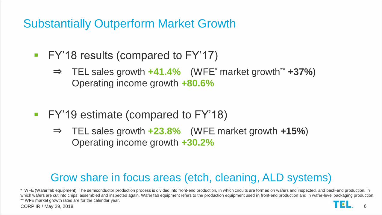
Substantially Outperform Market Growth
Grow share in focus areas (etch, cleaning, ALD systems)
FY’18 results (compared to FY’17)
⇒ TEL sales growth +41.4% (WFE* market growth** +37%)
Operating income growth +80.6%
FY’19 estimate (compared to FY’18)
⇒ TEL sales growth +23.8% (WFE market growth +15%)
Operating income growth +30.2%
* WFE (Wafer fab equipment): The semiconductor production process is divided into front-end production, in which circuits are formed on wafers and inspected, and back-end production, in
which wafers are cut into chips, assembled and inspected again. Wafer fab equipment refers to the production equipment used in front-end production and in wafer-level packaging production.
** WFE market growth rates are for the calendar year.

CORP IR / May 29, 2018 7
* WFE (Wafer fab equipment): The semiconductor production process is divided into front-end production, in which circuits are formed on wafers and inspected, and back-end production, in
which wafers are cut into chips, assembled and inspected again. Wafer fab equipment refers to the production equipment used in front-end production and in wafer-level packaging production.
Medium-term Management Plan Progress
Proceed according to plan in both strengthening competitiveness of products and raising profitability
WFE*
Market size $31B $37B $51B $58B $42B $45B
Net sales ¥663.9B ¥799.7B ¥1,130.7B ¥1,400.0B ¥1,050.0B ¥1,200.0B
Operating
margin17.6% 19.5% 24.9% 26.1% 24% 26%
ROE 13.0% 19.1% 29.0% - 20-25%
FY2016 (CY2015) market size does not include equipment for wafer-level packaging.
FY’16
(Actual)
FY’17
(Actual)
FY’20
financial modelFY’18
(Actual)
FY’19
(Estimate)
CORP IR / May 29, 2018 8
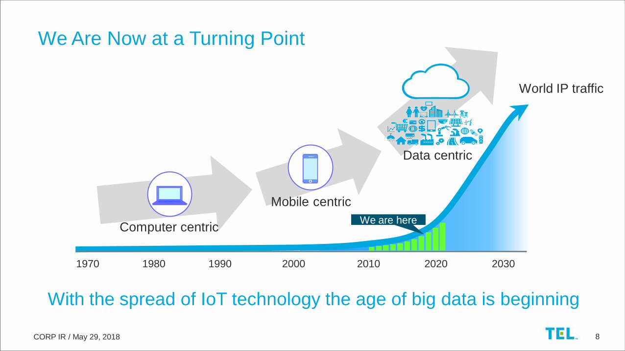
We Are Now at a Turning Point
1970 1980 1990 2000 2010 2020 2030
World IP traffic
With the spread of IoT technology the age of big data is beginning
Mobile centric
Computer centricWe are here
Data centric
CORP IR / May 29, 2018 9
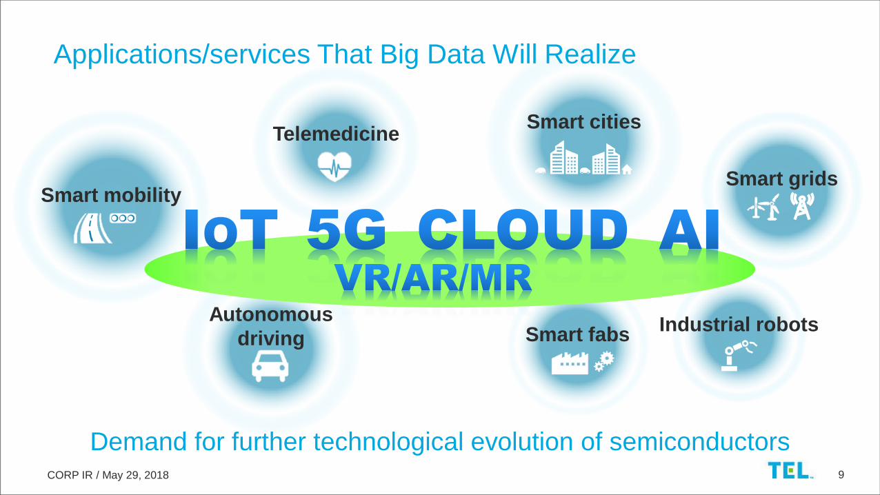
Smart fabsIndustrial robots
Smart mobilitySmart grids
Telemedicine
Applications/services That Big Data Will Realize
Demand for further technological evolution of semiconductors
Autonomous
driving
Smart cities

CORP IR / May 29, 2018 10
Big Investment in the Cloud
Continuing data growth (CAGR 27%**)
Necessary to replace servers every 5 years
Continued strong demand for memory
Hyperscale data center*
construction boom
338 ➡ 628CY2016 CY2021 Source: CISCO
locations
* CISCO’s definition: Operator with annual revenue of over $1B from IaaS/PaaS, over $2B from SaaS, over $4B from internet, search and social networking, and over $8B in e-commerce/payment processing
** Source: CISCO GCI2017.2 CAGR of data center traffic 2016-2021
CORP IR / May 29, 2018 11
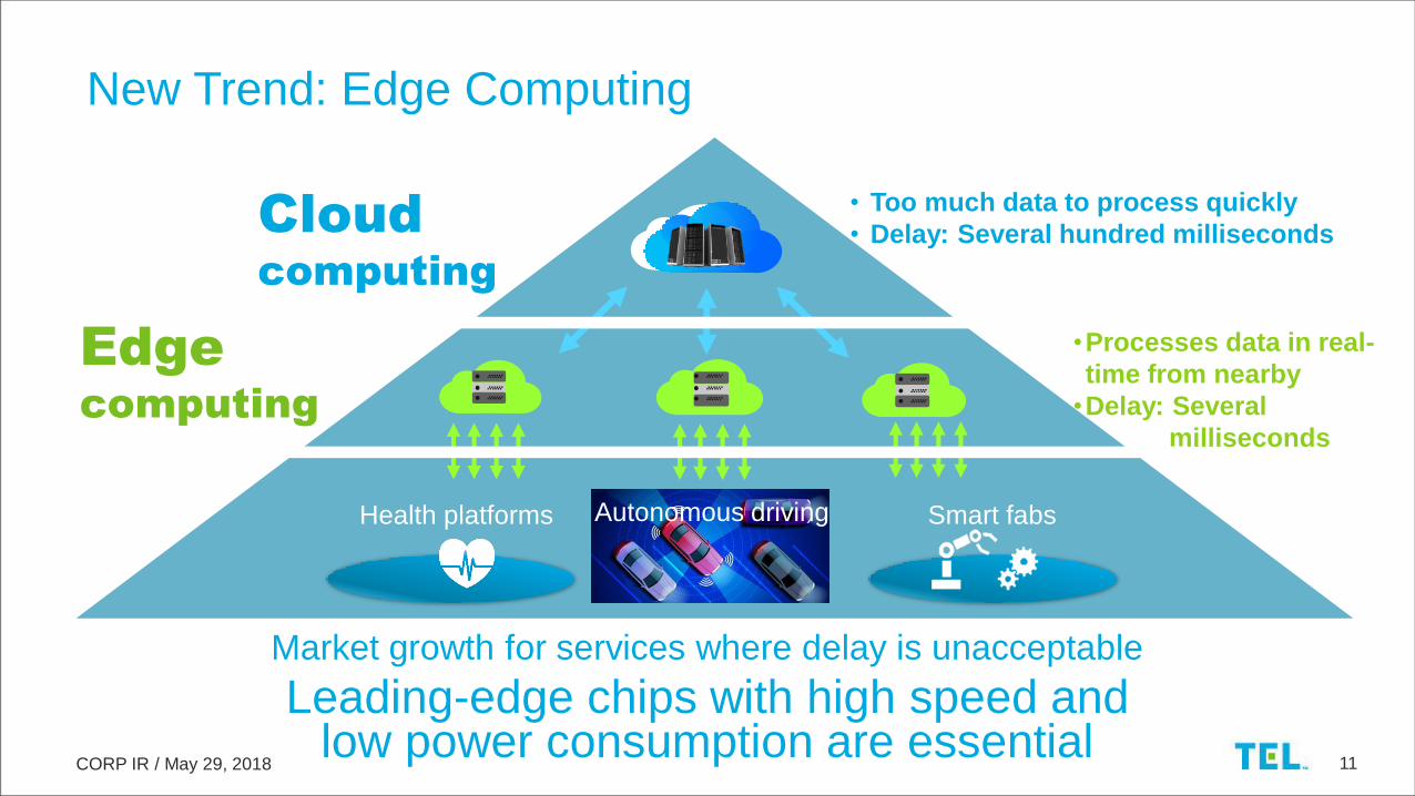
New Trend: Edge Computing
Market growth for services where delay is unacceptable
Leading-edge chips with high speed and low power consumption are essential
Autonomous drivingHealth platforms Smart fabs
Edge
computing
Cloud
computing
•Processes data in real-
time from nearby
•Delay: Several
milliseconds
• Too much data to process quickly
• Delay: Several hundred milliseconds

CORP IR / May 29, 2018 12
14/16nm 10nm 7nm
Logic
4X 6/7X 9X
3D NAND
2Z 1X 1Y
DRAM
Rising Added-value in SPE
Expanded business opportunities for SPE manufacturers on arrival of new applications and rising level of technological difficulty
WFE investment (100k WSPM*, greenfield/TEL estimate)
~$7B ~$7B
~$18B
* WSPM: Wafer starts per month

CORP IR / May 29, 2018 13
Designflexibility
FlexibleEdge bent
Increasingresolution
Mobile, VR: 300 ppi 1000 ppi
FHD 4K 8K
TV:
LCD OLED
TFT
Color filter
Backlight
LCD
TFT
Emissive
layer
Expanded business opportunities due to technological change
Higher Sophistication of Display Technologies
OLEDIncreasing
screen size
Flexible, edge bent, free format

CORP IR / May 29, 2018 14
WFE Market Outlook
$37B
$51B
$58B$61B $62B $63B
CY'16 CY'17 CY'18* CY'19* CY'20* CY'21* * TEL estimate
WFE market by application*
WLP
DRAM
Non-volatile memory
Logic foundry
Logic & others
(MPU, AP, others)
WFE market approaching $60B+ phase

CORP IR / May 29, 2018 15
WFE
Market size
Operating margin
Net sales
26.5%
30-35%
¥1,500.0B
28%
¥1,700.0B
ROE
$55B $62B
New Financial Model (FY2021)
Aim for a world class operating margin of 30%+
in the medium- to long-term

CORP IR / May 29, 2018 16
Business development in focus areas is making good progress, and achievement
of the financial model announced in May 2017 is in sight
Over the past year it has become widely recognized that the semiconductor
industry has entered a new growth stage on the expansion of new applications
that support social infrastructure such as AI and IoT
On outlook for further growth in the semiconductor industry we have upwardly
revised our expected WFE market size to $62B in FY2021
Even if WFE should shrink to $55B due to temporary market shifts, we will aspire to a management structure that is able to flexibly respond to market shifts and to secure net sales of ¥1,500.0B and an operating margin of 26.5%
Rationale for Revisions to Financial Model
Establish new financial model based on further market growth and opportunities for significant growth for TEL
CORP IR / May 29, 2018 17
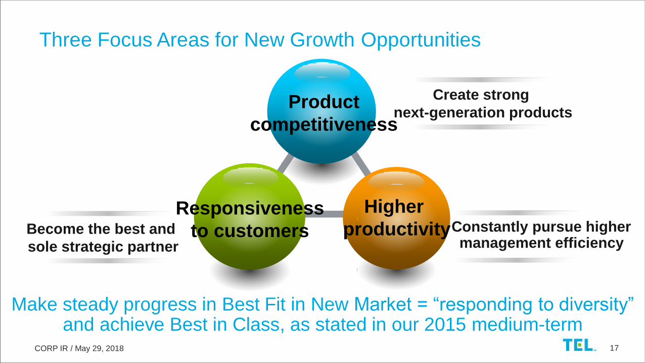
Three Focus Areas for New Growth Opportunities
Constantly pursue higher management efficiency
Become the best and
sole strategic partner
Create strong
next-generation products
Higher
productivity
Product
competitiveness
Responsiveness
to customers
Make steady progress in Best Fit in New Market = “responding to diversity” and achieve Best in Class, as stated in our 2015 medium-term
CORP IR / May 29, 2018 18
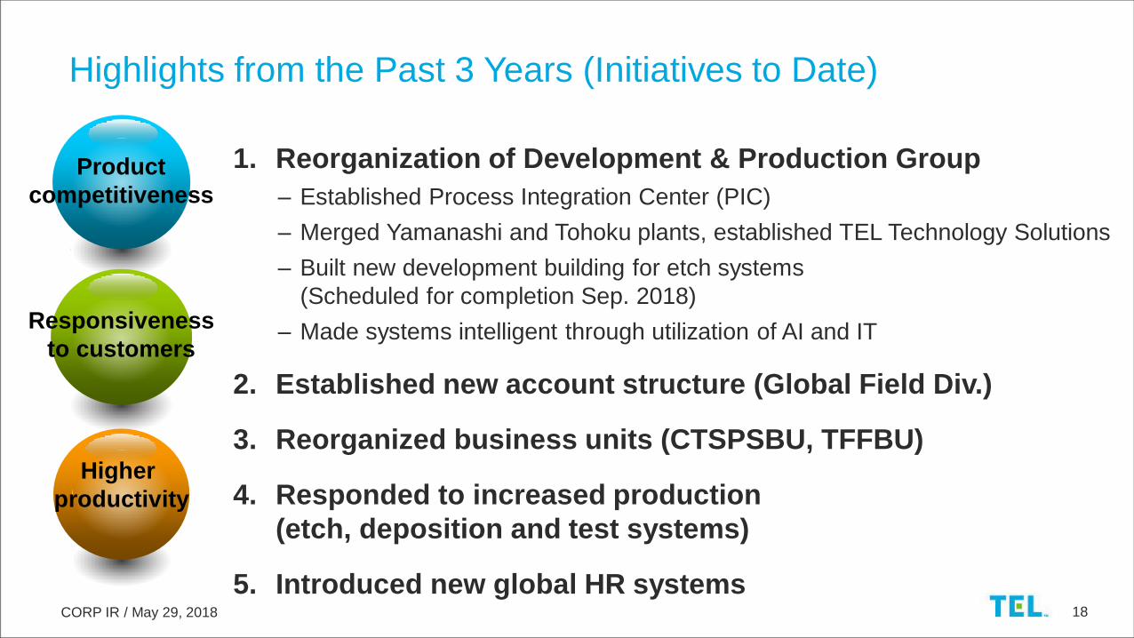
Highlights from the Past 3 Years (Initiatives to Date)
Higher
productivity
1. Reorganization of Development & Production Group
– Established Process Integration Center (PIC)
– Merged Yamanashi and Tohoku plants, established TEL Technology Solutions
– Built new development building for etch systems
(Scheduled for completion Sep. 2018)
– Made systems intelligent through utilization of AI and IT
2. Established new account structure (Global Field Div.)
3. Reorganized business units (CTSPSBU, TFFBU)
4. Responded to increased production
(etch, deposition and test systems)
5. Introduced new global HR systems
Product
competitiveness
Responsiveness
to customers

CORP IR / May 29, 2018 19
Further Promotion of Our 3 Focus Areas (Future Initiatives)
Higher
productivity
1. Promote development of technologies that leverage
TEL’s comprehensive strengths – Process integration technology that unites diverse technologies
– Develop next generation platforms
2. Promote early stage joint development and evaluation
with customers– Share roadmap for multi-generational technologies: shift collaboration
“from dots to lines”
– Expand onsite evaluation activity
3. Increase productivity and added-value using data and AI
4. Respond to growing China business
5. Increase earnings in field solutions business
6. Promote efficiency though launch of business reform project
7. Implement medium-term incentive plan
Product
competitiveness
Responsiveness
to customers

CORP IR / May 29, 2018 20
Field Solutions (FS)
Leverage our strengths as an equipment manufacturer to
increase earnings in both the used equipment/modification
and part/service segments
Business strategy
93.0105.0 115.0
150.0165.0
190.077.0
80.093.0
101.0
115.0
150.0
0
100
200
300
400
FY'15 FY'16 FY'17 FY'18 FY'19(E)
Field Solutions sales
¥340.0B
170.0
Used equipment
and modification
Parts and services
185.0208.0
251.0
WFE$62B
FY’21
(Target)
280.0
Respond to new customer needs
driven by IoT
– Provide upgrades and
remanufactured equipment that
handle new applications
Contribute to improving customer
productivity
– Provide added-value services using
remote connections
(Installed base of 66,000 units)
CORP IR / May 29, 2018 21
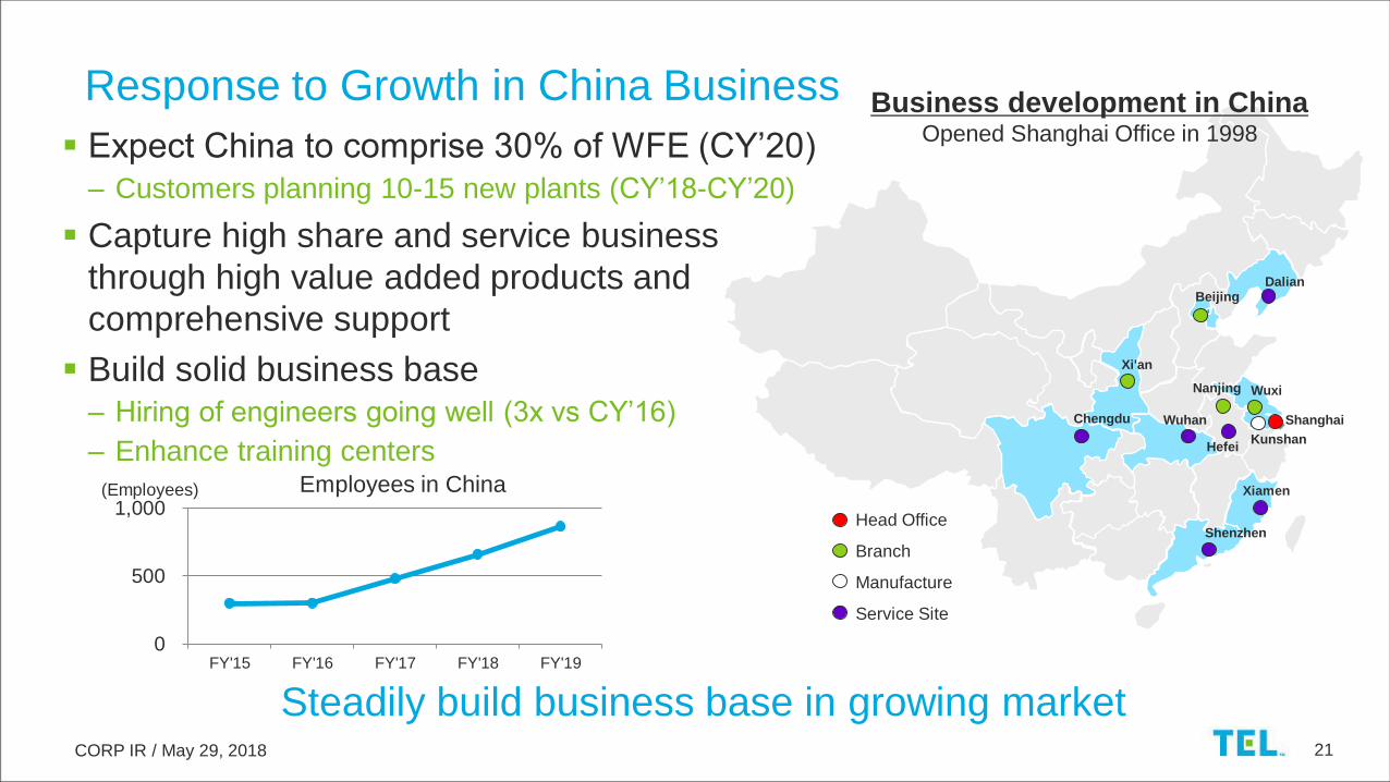
Expect China to comprise 30% of WFE (CY’20)– Customers planning 10-15 new plants (CY’18-CY’20)
Capture high share and service business
through high value added products and
comprehensive support
Build solid business base – Hiring of engineers going well (3x vs CY’16)
– Enhance training centers
Response to Growth in China Business
Beijing
Shanghai
Wuxi
Chengdu Wuhan
Kunshan
Xiamen
Xi'an
Nanjing
Head Office
Branch
Manufacture
Service Site
0
500
1,000
FY'15 FY'16 FY'17 FY'18 FY'19
Employees in China
Business development in ChinaOpened Shanghai Office in 1998
Dalian
Hefei
Shenzhen
Steadily build business base in growing market
(Employees)
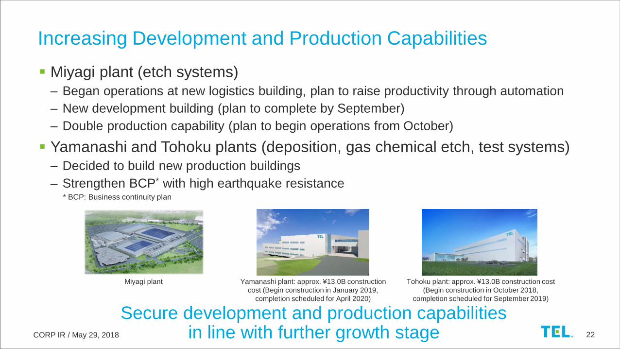
CORP IR / May 29, 2018 22
Miyagi plant (etch systems)– Began operations at new logistics building, plan to raise productivity through automation
– New development building (plan to complete by September)
– Double production capability (plan to begin operations from October)
Yamanashi and Tohoku plants (deposition, gas chemical etch, test systems)– Decided to build new production buildings
– Strengthen BCP* with high earthquake resistance
Increasing Development and Production Capabilities
Yamanashi plant: approx. ¥13.0B construction
cost (Begin construction in January 2019,
completion scheduled for April 2020)
Tohoku plant: approx. ¥13.0B construction cost
(Begin construction in October 2018,
completion scheduled for September 2019)
Miyagi plant
Secure development and production capabilities in line with further growth stage
* BCP: Business continuity plan

CORP IR / May 29, 2018 23
TEL’s Sustainability (economic value × social value = corporate value creation)
Environment Climate change, water, biodiversity, environmental management
SocialHuman rights, employment and labor, health and safety, supply chain,
local communities
Governance Corporate governance, compliance, risk management
Going forward, continue to work to resolve social issues and contribute to the
achievement of sustainable development goals (SDGs) through our business
activities in accordance with the Ten Principles of the UN Global Compact and RBA*
code of conduct
Continue to be a company trusted by all stakeholders* RBA: Responsible business alliance

CORP IR / May 29, 2018 24
Contributing to the Environment is a Key Strategy
Technological proposals that reduce environmental impact create significant value
Lower energy consumption
of TEL products
Manufactured devicesrealize low power
consumptionRaises TEL’s value+
CORP IR / May 29, 2018 25
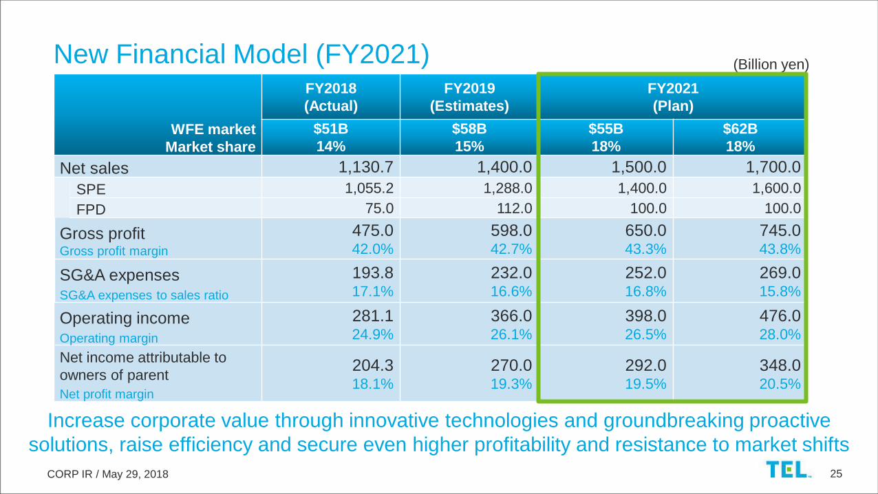
New Financial Model (FY2021) (Billion yen)
FY2018
(Actual)
FY2019
(Estimates)
FY2021
(Plan)
$51B
14%
$58B
15%
$55B
18%
$62B
18%
Net sales 1,130.7 1,400.0 1,500.0 1,700.0
SPE 1,055.2 1,288.0 1,400.0 1,600.0
FPD 75.0 112.0 100.0 100.0
Gross profitGross profit margin
475.042.0%
598.042.7%
650.043.3%
745.043.8%
SG&A expensesSG&A expenses to sales ratio
193.817.1%
232.016.6%
252.016.8%
269.015.8%
Operating incomeOperating margin
281.124.9%
366.026.1%
398.026.5%
476.028.0%
Net income attributable to
owners of parent
Net profit margin
204.318.1%
270.019.3%
292.019.5%
348.020.5%
Increase corporate value through innovative technologies and groundbreaking proactive
solutions, raise efficiency and secure even higher profitability and resistance to market shifts
WFE market
Market share

CORP IR / May 29, 2018 26
Raise gross profit margin of core SPE, FPD products
– Timely introduction of new products to an expanding market
– Lower cost ratio through product quality improvements
Gross Profit, SG&A Expenses (Sales ¥1,700.0B Model)
FY2018
(Actual)
FY2019
(Estimates)
FY2021
(Plan)
Growth rate
(FY’18-FY’21)
Gross profit
Gross profit margin
475.042.0%
598.042.7%
745.043.8%
+57%+1.8pts
(Billion yen)
Proactively invest in growth areas while planning appropriate SG&A and
R&D expenses
FY2018
(Actual)
FY2019
(Estimates)
FY2021
(Plan)
Growth rate
(FY’18-FY’21)
SG&A expenses
SG&A expenses to sales ratio
193.817.1%
232.016.6%
269.015.8%
+39%-1.3pts
(Billion yen)

CORP IR / May 29, 2018 27
39.5
21.7
12.7 13.1 13.3
20.6
45.651.0
24.1 26.6 24.820.8 19.2 17.8
20.626.0
0
20
40
60
FY’12 FY’13 FY’14 FY’15 FY’16 FY’17 FY’18 FY’19 (E) FY’21
81.573.2 78.6
71.3 76.283.8
97.1
120.0
0
50
100
150
FY'12 FY'13 FY'14 FY'15 FY'16 FY'17 FY'18 FY'19 (E) FY'21
R&D Expenses, Capex Plan
Conduct proactive investment towards further growth
(Billion Yen)
(Billion Yen)
R&D expenses
Capex Depreciation
(Plan)
(Plan)
130.0-145.0
40.0-50.0
35.0-37.0

CORP IR / May 29, 2018 28
Accounts receivable turnover
– Current: 52 days⇒ Achieved target
Inventory turnover
– Current: 111 days ⇒ Target: 95 days
ROE
– Current: 29% ⇒ Target: 30-35%
Assets and Capital Efficiency (Sales ¥1,700.0B Model)
EPS and ROE(Yen)
461
702
1,245
13.0%
19.1%
29.0%
0
500
1,000
1,500
2,000
2,500
FY'16 FY'17 FY'18 FY'21(Target)
EPS ROE
Maintain focus on assets and capital efficiency
ROE = (Net income attributable to owners of parent/Average total equity) x 100
30-35%

CORP IR / May 29, 2018 29
Approach to capital policy
– While closely monitoring the business environment and our necessary cash balance, we
will strive to raise ROE through earnings maximization and by raising capital efficiency
Approach to shareholder return policy (basically linked to performance)
Capital Policy, Shareholder Returns
No change in shareholder return policy
Dividend payout ratio: 50%
Annual DPS of not less than ¥150
We will review our policy if the company does not generate net income for 2 consecutive fiscal years
We will flexibly consider share buybacks
CORP IR / May 29, 2018 30
Establish new financial model backgrounded by expected
growth in semiconductor and production equipment markets.
Aim for short, medium and long term growth
Aim to increase sales beyond market growth rate through
stronger competitiveness of products and deeper cooperation
with customers
Raise development efficiency and business productivity and
secure even higher profitability and resistance to market shifts
Summary
Aim for sustained growth in corporate value througha management base with global-standard strength
CORP IR / May 29, 2018 31
May 29, 2018
Akihisa Sekiguchi, Ph.D.
VP & GM, Deputy General Manager, Technology Strategy Division,
Advanced Semiconductor Technology Division, Global R&D
Evolving Semiconductor Device Application and
the Future of Process Technology

CORP IR / May 29, 2018 32
Outline
Trends and issues in semiconductor process technology:
Mainstream devices (CMOS Logic, NAND, DRAM)
Technology challenges deep dive: Logic devices
Devices that may drive further growth of the WFE market in the future
autonomous driving enablers and AI
Summary

CORP IR / May 29, 2018 33
Trends and Issues in Semiconductor Process Technology

CORP IR / May 29, 2018 34
Process Technology Issues for Major Semiconductor Devices
High selectivity process
Realizing highly uniform
process suitable for 3D
structures
High aspect ratio process,
enhanced precision and
material specific adaptation to
achieve higher bit density
Precision patterning process
co-optimized for device design
and new materials
5 & 3 nm developmentEnhancements from 1Y-1ZMulti-layering & productivity
Drive collaboration in & out of the company to accelerate creation of
innovative process technologies
3D NAND DRAM Logic

CORP IR / May 29, 2018 35
Staircase formation
Multi Level
Contact formation
SiN removal
Isolation/Source line formation
3D NAND Technical Issues
Stress management
& Multi-stacking
Logic
under Cell
Etch Trim Etch Trim …
Etch
Trim
ONON etch
Channel formation
& Cell gate stack
ONON etch
Isolation,
Metallization
Tunnel oxide
Channel depHigh-k dielectric,
Metallization
MLC etch
Increasing number of layers requires a variety of new technical solutions
1st
tier
2nd
tier
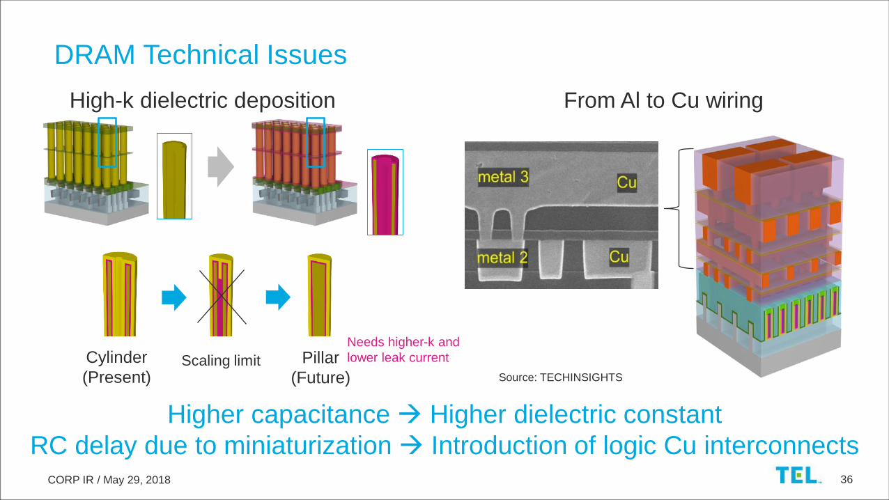
CORP IR / May 29, 2018 36
DRAM Technical Issues
Higher capacitance Higher dielectric constant
RC delay due to miniaturization Introduction of logic Cu interconnects
High-k dielectric deposition
Scaling limitCylinder
(Present)
Pillar
(Future)
From Al to Cu wiring
Source: TECHINSIGHTS
Needs higher-k and
lower leak current
CORP IR / May 29, 2018 37
Technology Challenges Deep Dive: Logic Devices
CORP IR / May 29, 2018 38
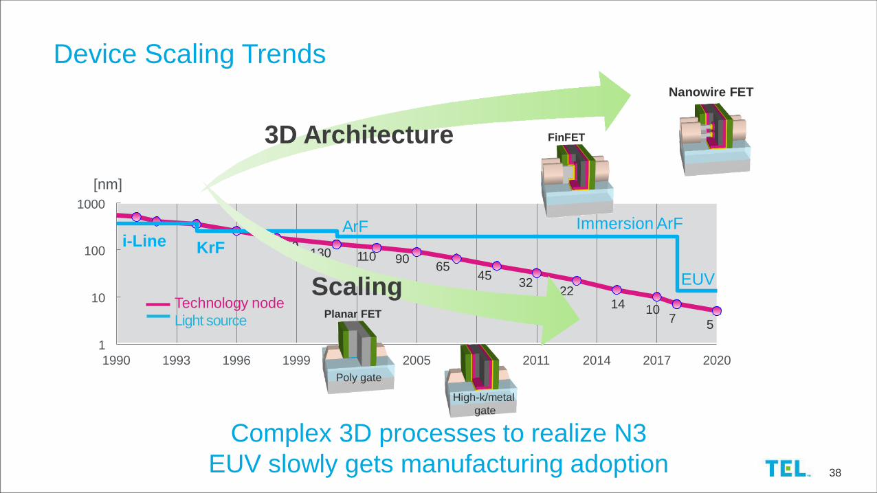
Device Scaling Trends
180130 110 90
6545
3222
14 107
5
1
10
100
[nm]
1000
1990 1993 1996 1999 2002 2005 2008 2011 2014 2017 2020
Technology node
Light source
i-LineArF
EUV
Immersion ArF
KrF
Planar FET
Poly gate
High-k/metal
gate
Scaling
3D Architecture
Complex 3D processes to realize N3
EUV slowly gets manufacturing adoption
FinFET
Nanowire FET
CORP IR / May 29, 2018 39
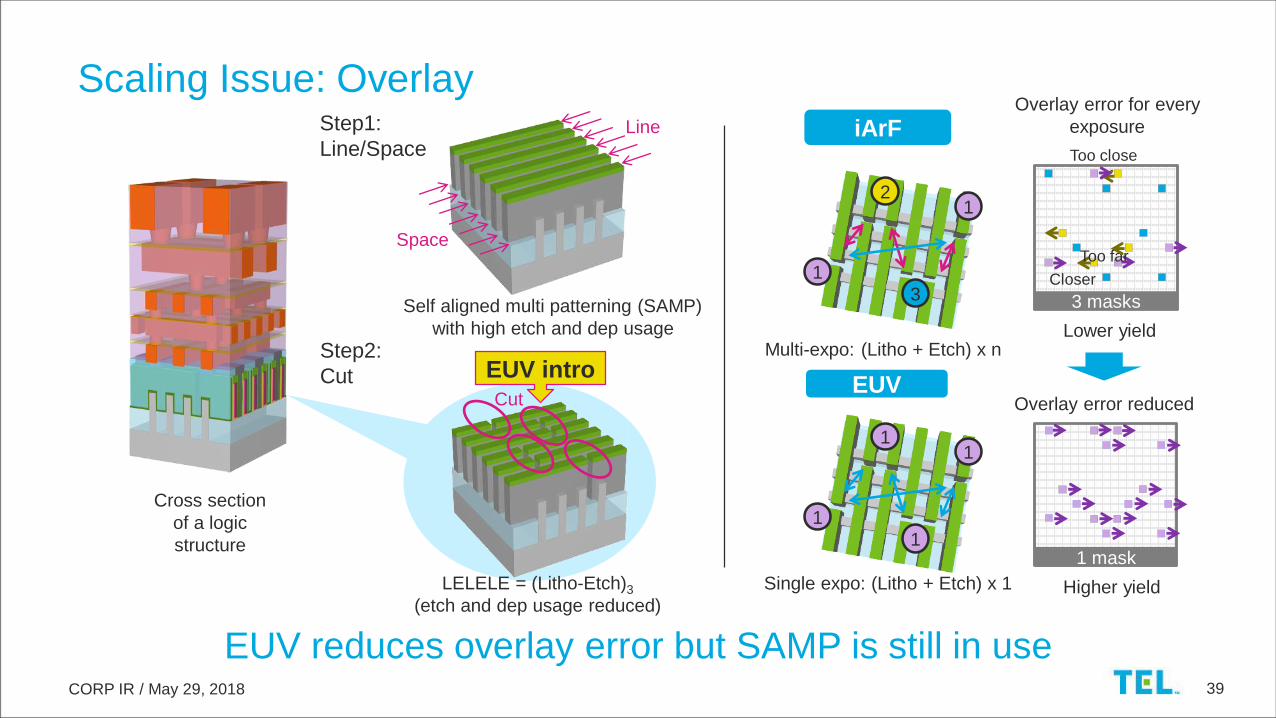
Line
Space
Scaling Issue: Overlay
Cut
Multi-expo: (Litho + Etch) x nLower yield
Higher yield
Overlay error reduced
Cross section
of a logic
structure
EUV intro
iArF
EUV
Self aligned multi patterning (SAMP)
with high etch and dep usage
LELELE = (Litho-Etch)3
(etch and dep usage reduced)
Step1:
Line/Space
Step2:
Cut
Single expo: (Litho + Etch) x 1
Overlay error for every
exposure
1
12
3
1
11
1
3 masks
Too close
Closer
Too far
1 mask
EUV reduces overlay error but SAMP is still in use

CORP IR / May 29, 2018 40
Logic FEOL/MOL Technology Roadmap
Node
Transistor
Contact
< 3.5 nm5 nm7 nm10 nm16-14 nm
Nanowire/Nanosheet FET
Diamond
shaped Epi
Wrap around contact
W Co and other materials
FinFET
Scaling and performance enhancement concurrently requires structure, design and material changes, which makes integration challenging

CORP IR / May 29, 2018 41
Complexity of the Fabrication Processes for Logic Devices
Applications N+1 N+2 N+3
FEOL Patterning and hard mask
Nanowire FET
MOL Patterning and hard mask
Contact structure (WAC)
New plug material (Ru)
BEOL Patterning and hard mask
EUV productivity
Selective deposition
Common Pitch imbalance control
Wrap around contact (WAC)
Courtesy of imec
Multi-color patterning
Known Unknown
Conventional patterning
Nanowire FET
R. Coquand et al.,
VLSI tech. 2013
Self-aligned contact (SAC)
Precise control in an atomic level
Design and process technology co-optimization is a challenging integration issue

CORP IR / May 29, 2018 42
Major Semiconductor Devices: FinFET
FinFET formation alone is a complicated process

CORP IR / May 29, 2018 43
Challenges in Nanowire/Nanosheet Fabrication
Nanowire/Nanosheet FET
Dummy gate removalSiGe removal
by chemical dry etchOxidation for roundingOxide removalHigh-k dielectric
+ metal dep
FinFET
Dummy gate removalHigh-k dielectric
+ metal dep
Nanowire/Nanosheet formation is even more complicated than FinFET
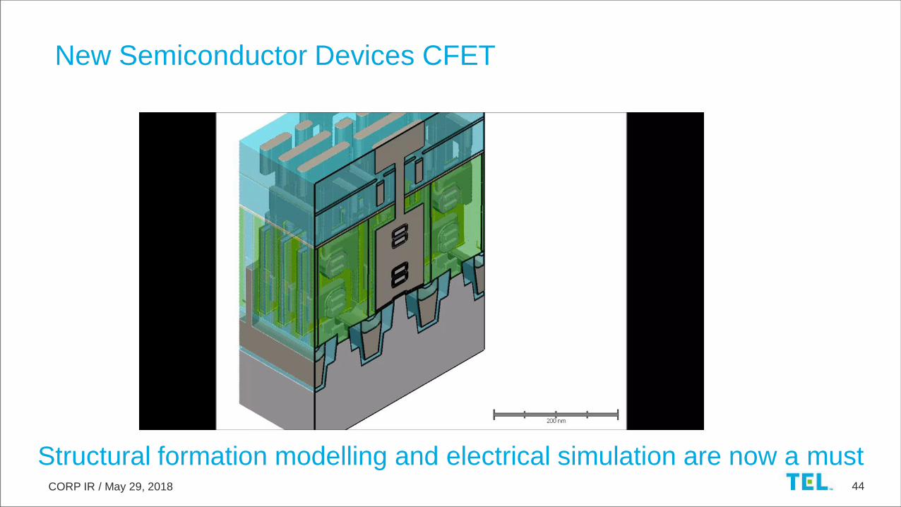
CORP IR / May 29, 2018 44
New Semiconductor Devices CFET
Structural formation modelling and electrical simulation are now a must

CORP IR / May 29, 2018 45
Logic BEOL Technology Roadmap
Node
Patterning
Metallization
< 3.5 nm5 nm7 nm10 nm16-14 nm
Self-aligned via (SAV)
Fully self-aligned via (FSAV)
Cu: ECD
Ta/TaN PVD
Replacement of Cu:
Ru, Co, CoAl
Non SAV SAV
Cu Post Cu
Estimated using IEDM, VL, IITC papers
Self-aligned block
(SAB)
Dual damascene
Scaling and overlay issues require new integration schemesTEL’s estimates using IEDM, VLSI symposium, IITC papers

CORP IR / May 29, 2018 46
R&D for Future Growth: Beyond Cu
Line width reduction is pushing copper to its limits
New material required
Source: An Steegen, imec technology forum 2017

CORP IR / May 29, 2018 47
New Opportunities through Integration
CFET (new structure)
Buried power rail (new material)
Close integration between process equipment is a must in order to propose solutions to realize further scaling
through new materials and structural solutions
Cleaning
Etch
Lithography
Deposition
CELLESTA™-i
CLEAN TRACK™
LITHIUS Pro™ Z
TELINDY PLUS™
NT333™
Certas™
Tactras™ Vigus™
EXIM™
EXPEDIUS™-i
Triase+™
Source: Imec presentation at ISPD 2016
Source: imec
Sn
Dn
Sp
Dp
Sn
Dn
Sp
Dp

CORP IR / May 29, 2018 48
Devices That May Drive Further Growth of the WFE Market
in the Future Autonomous Driving Enablers and AI

CORP IR / May 29, 2018 49
https://blog.caranddriver.com/nhtsa-sides-with-google-officially-declares-autonomous-car-software-a-driver-sorta/
Autonomous Driving
Semiconductor usage will increase
with the arrival of autonomous driving

CORP IR / May 29, 2018 50
Hybrid vehicles use 2.5-3 times more semiconductor
devices compared to conventional gasoline vehicles
Electric vehicles use even more than 2x
With ADAS*, additional value add is $50-$100
Autonomous driving vehicles transit 6TB of data daily to
Data Centers
Higher Automotive Functionality
* ADAS: Advanced driver assistance system• ADAS today uses 6 cameras per vehicle
• In the near future, ~10 per vehicle
Interior, driver, passenger monitoring
AR/VR
Airbag control
Increase in semiconductor usage from conventional gasoline, hybrid, electrical, to autonomous vehicles
(not to mentions the infotainment data related adders)
Surrounded
view
Park assist
Surrounded view
Rear collision
warning
Em
erg
en
cy b
rea
kin
g
Pe
de
stria
n d
ete
ctio
n
Co
llisio
n a
vo
ida
nce
Surrounded
view
Park assist
by ultrasound
Park assist
by ultrasound
Cross traffic assist
Traffic
sign
recognition
Lane
departure
warning
Adaptive
cruise control
/LRR

CORP IR / May 29, 2018 51
Viewing, Sensing camera
– Front 1-2, back1-3, CIS
– In the future 10-12
– Higher pixel density
– Faster image readout
– Processing circuit
ADAS・Device Challenges for Autonomous Driving
mm radar
– Higher resolution, wider angle
– From SiGe to Si CMOS (~2019)
– Integrated communication IC and micro controller
(~2022)
LiDAR* cost
(Infrared laser scan in 3D)
– High end LiDAR: ~few million yen
– Motorless MEMS version will drive cost
below 50,000 yen
Processor/Memory/ECU**
– CPU under autonomous driving use a few KW
– DRAM degradation under high temp (refresh cycle)
– Using auto temperature grade LPDDR4• High temp tolerant DRAM cell
• Error reduction circuit
• Data/ECC*** transmission function
– Flexible ECU development2016 2025
GaAs
SiGeSi CMOS
integration$50
$200
* LiDAR: Laser imaging detection and ranging ** ECU: Engine control unit *** ECC: Error correction code
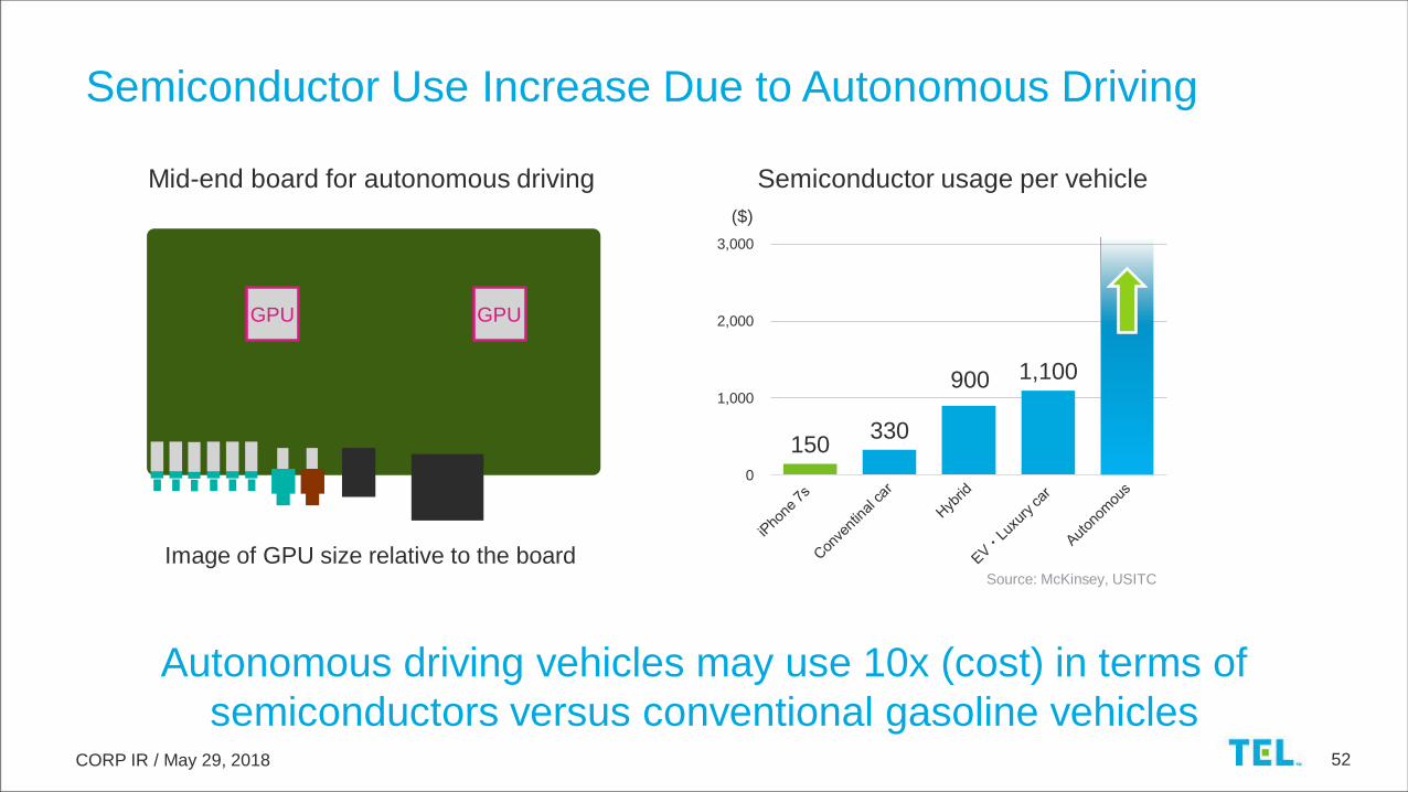
CORP IR / May 29, 2018 52
150 330
900 1,100
0
1,000
2,000
3,000
Source: McKinsey, USITC
Semiconductor Use Increase Due to Autonomous Driving
Autonomous driving vehicles may use 10x (cost) in terms of
semiconductors versus conventional gasoline vehicles
Mid-end board for autonomous driving
GPU GPU
Image of GPU size relative to the board
Semiconductor usage per vehicle
($)

CORP IR / May 29, 2018 53
Semiconductor Sales Amount
346
420
470 502 493 497
520
9.9%9.3% 9.2% 9.6%
10.8%
11.9%12.4%10.0% 9.8% 9.9% 10.1%
11.2%12.1%
12.8%
0%
5%
10%
15%
20%
0
100
200
300
400
500
600
2016 2017 2018 2019 2020 2021 2022
Military/Civil Aerospace
Industrial
Data Processing
Consumer
Communication
Automotive
Automotive rate
Industrial rate
($B)
Automotive semiconductor CAGR 10.5%
Industrial app semiconductor CAGR 10.1%
CAGR* (2017-2022) 4.3%
Worldwide Semiconductor Sales Estimate
Source (Worldwide Semiconductor Forecast): Gartner, “Semiconductor Forecast Database, Worldwide, 1Q18 Update”, 3 April 2018,
Charts/graphics created by Tokyo Electron based on Gartner research
Semiconductor market will continue to grow nicely in the future
CY’16 CY’17 CY'18 CY'19 CY'20 CY'21 CY'22
* CAGR: Compound annual growth rate
CORP IR / May 29, 2018 54
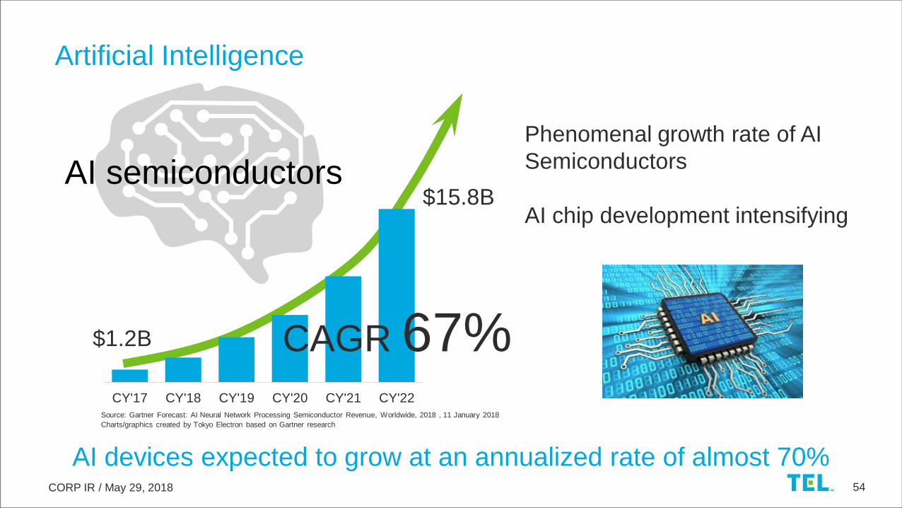
Artificial Intelligence
Phenomenal growth rate of AI
Semiconductors
AI chip development intensifying
CY'17 CY'18 CY'19 CY'20 CY'21 CY'22
CAGR 67%
$15.8B
$1.2B
AI semiconductors
Source: Gartner Forecast: AI Neural Network Processing Semiconductor Revenue, Worldwide, 2018 , 11 January 2018
Charts/graphics created by Tokyo Electron based on Gartner research
AI devices expected to grow at an annualized rate of almost 70%
CORP IR / May 29, 2018 55
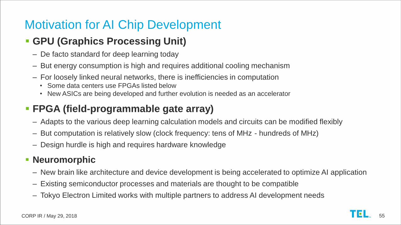
GPU (Graphics Processing Unit)
– De facto standard for deep learning today
– But energy consumption is high and requires additional cooling mechanism
– For loosely linked neural networks, there is inefficiencies in computation• Some data centers use FPGAs listed below
• New ASICs are being developed and further evolution is needed as an accelerator
FPGA (field-programmable gate array)
– Adapts to the various deep learning calculation models and circuits can be modified flexibly
– But computation is relatively slow (clock frequency: tens of MHz - hundreds of MHz)
– Design hurdle is high and requires hardware knowledge
Neuromorphic
– New brain like architecture and device development is being accelerated to optimize AI application
– Existing semiconductor processes and materials are thought to be compatible
– Tokyo Electron Limited works with multiple partners to address AI development needs
Motivation for AI Chip Development

CORP IR / May 29, 2018 56
New semiconductor devices will grow WFE market
over the medium- to long- term
WFE Outlook
$37B
$51B
$58B$61B $62B $63B
CY'16 CY'17 CY'18* CY'19* CY'20* CY'21* * TEL estimate
WFE by application*
WLP
DRAM
Non-volatile memory
Foundry logic
Logic & others
(MPU, AP and others)

CORP IR / May 29, 2018 57
Summary

CORP IR / May 29, 2018 58
Summary – Diversity of Semiconductor Technology
MoreMoore
Functional diversificationC
MO
S s
calin
gMore than Moore
Logic with new material
new structure
Advanced packaging
(3DI/WLP)
Emerging
memoryPatterning
Heterogeneous
3DIFlip-Chip
2.5D
Wire-bonding
Si photonics
Homogeneous
DRAM
NAND
STT-MRAM
3D NAND
ReRAM
Strained Si
High-k metal
gate
Cu/ULK
FinFET
Nanowire FETCu/ELK
ArF
Arf-immersion
EUV
DP/MP
NIL, EBDWDSA,
KrF
Now
2017~
InFO
Neuromorphic
CFET
59
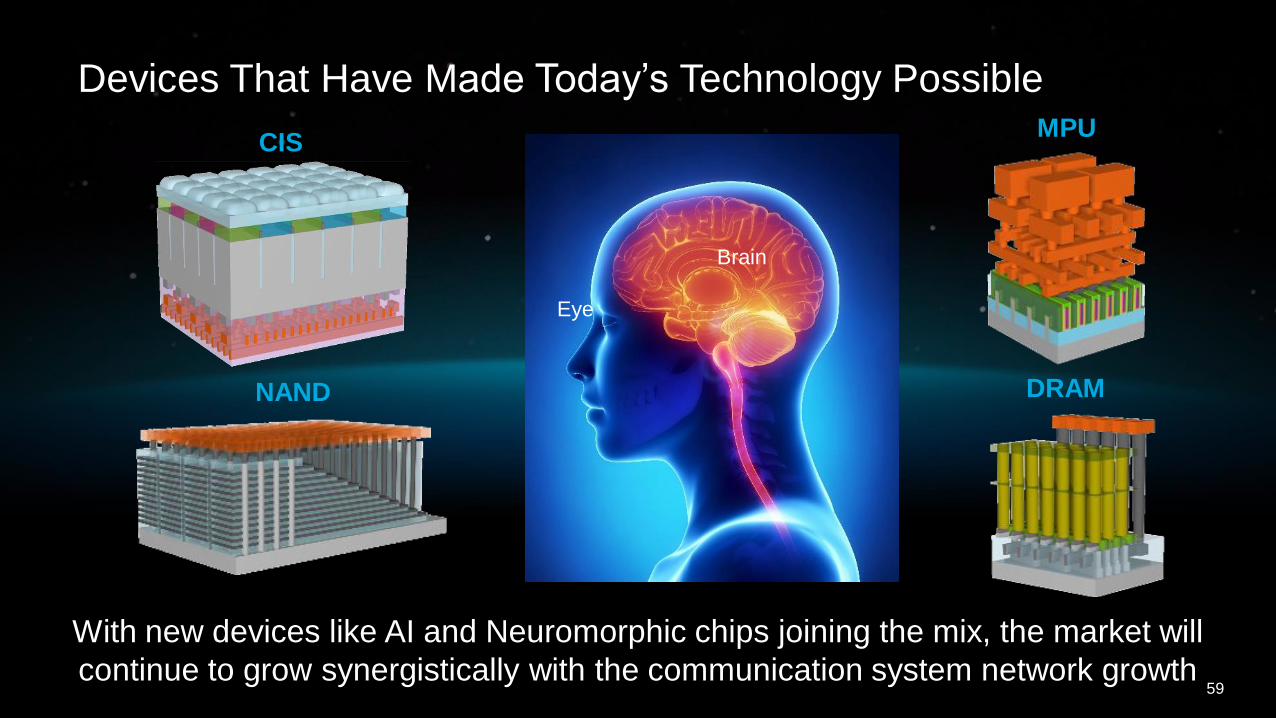
Devices That Have Made Today’s Technology Possible
DRAM
NAND
Brain
MPUCIS
Eye
NAND
With new devices like AI and Neuromorphic chips joining the mix, the market will
continue to grow synergistically with the communication system network growth

60
Technology Evolution at a Glance
PC
Mobile
AR/MRVR
FinTech
Cloud
Network
Data
AI
Autonomous
driving
Robotics
RPA
Quantum
computing
Neuromorphic
Cybernetics
Bionics

CORP IR / May 29, 2018 61
May 29, 2018
Seisu (Yoh) Ikeda
SVP & GM, Deputy General Manager, Business Division, General Manager, CTSPS BU
Coater/developer, Cleaning System Business Strategy

CORP IR / May 29, 2018 62
Batch cleaning system
EXPEDIUS™-i
2.3 3.0 3.5 3.6 3.7 3.81.4 1.8 2.0 2.1 2.2 2.2
37
51
58 61 62 63
6% 6% 6% 6% 6% 6%
4%4% 4% 4% 4% 4%
0%
5%
10%
0
10
20
30
40
50
60
70
2016 2017 2018 2019 2020 2021
Coater/developer and Cleaning Systems Market Outlook
Coater/developer
SAM
Composition
ratio
Cleaning
SAM
Composition
ratio
TEL’s coater/developer and cleaning
SAM* in WFE market($B)
Coater/developer
– Introduction of EUV lithography for mass production
– Established regional offices in China and expanded
support for customers
Cleaning system
– Growth in wet etch market for 3D NAND
– Increased demand for bevel cleaning
– Further demand for drying technology that prevents
pattern collapse accompanying miniaturization
Coater/developer
CLEAN TRACK™
LITHIUS Pro™ Z
Single wafer
cleaning system
CELLESTA™-i
Growth in coater/developer and cleaning systems markets on demand for increasing density of semiconductor components
CY’16 CY’17 CY’18 CY’19 CY’20 CY’21
TEL estimate* SAM: Served available market
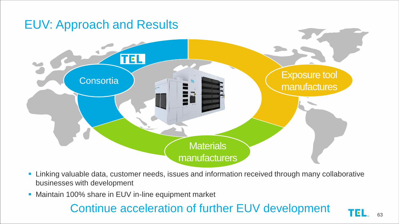
CORP IR / May 29, 2018 63
Linking valuable data, customer needs, issues and information received through many collaborative
businesses with development
Maintain 100% share in EUV in-line equipment market
EUV: Approach and Results
Exposure tool
manufactures
Materials
manufacturers
Consortia
Continue acceleration of further EUV development

CORP IR / May 29, 2018 64
Changing Issues in Introduction of EUV Mass Production(announced at EUVL Symposium)
Priority 2014 2015 2016 2017
1
Reliable source
operation with > 75%
availability
Reliable source
operation with > 85%
availability
Reliable source
operation with > 85%
availability
Resist resolution,
stochastics, and sensitivity
met simultaneously
2
Resist resolution,
sensitivity & LER* met
simultaneously
Resist resolution,
sensitivity & LER met
simultaneously
Resist resolution,
sensitivity & LER met
simultaneously
Reliable source > 250W
operation with > 90%
availability
3
Mask yield & defect
inspection/review
infrastructure
Mask yield & defect
inspection/review
infrastructure
Keeping mask defect free Keeping mask defect free
4 Keeping mask defect free Keeping mask defect free
Mask yield & defect
inspection/review
infrastructure
Mask yield & defect
inspection/review
infrastructure
* LER: Line edge roughness
Importance of resist performance and coater/developer technology increasing within EUV process
Source: 2017 EUVL Symposium Closing Remarks
CORP IR / May 29, 2018 65
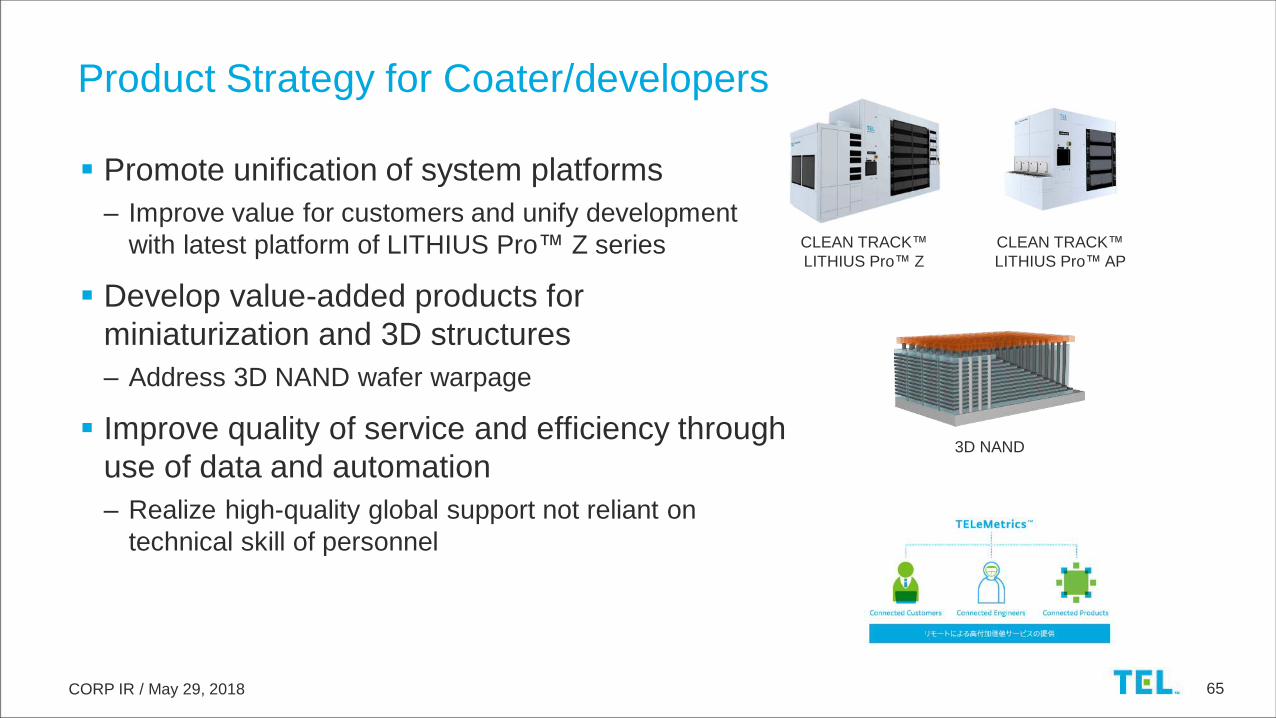
Promote unification of system platforms
– Improve value for customers and unify development
with latest platform of LITHIUS Pro™ Z series
Develop value-added products for
miniaturization and 3D structures
– Address 3D NAND wafer warpage
Improve quality of service and efficiency through
use of data and automation
– Realize high-quality global support not reliant on
technical skill of personnel
Product Strategy for Coater/developers
CLEAN TRACK™
LITHIUS Pro™ AP
CLEAN TRACK™
LITHIUS Pro™ Z
3D NAND

CORP IR / May 29, 2018 66
CY’17 market share: 25% (YoY+5pts, achieved medium-term plan early)
– Expand sales of CELLESTA™ single wafer
cleaning system• Bevel cleaning*: Improved yield around extreme edge of
wafer
• Post-etch cleaning for memory: improved productivity
• Apply best known coater/developer methods to cleaning
system business Share leading-edge technology and expertise by unifying
development
– Expand sales of EXPEDIUS™ batch cleaning system• Contribute to improved productivity of 3D NAND
• Improve wet etch performance and contribute to
enhanced yield
Growth of TEL’s Cleaning Business
Market shareCY’15
(Actual)
CY’16
(Actual)
CY’17
(Actual)・・・
CY’20
(Target)
Cleaning system 18% 20% 25% 27%+ 300mm
wafer
Extreme edge of wafer
(enlarged)
Wafer
Wafer
Bevel cleaning
Pre-clean
Post-clean
(single wafer cleaning system CELLESTA™ )
* Bevel cleaning: process for removing unnecessary film from the outer part of the wafer
Due to increasing number of films stacked on
wafer, films on a wafer’s extreme edge
become defects, affecting yield
Established leading positon in developing
equipment for accurate removal of film from a
wafer’s extreme edge, improving yield for
customers

CORP IR / May 29, 2018 67
Increased impact on wafer edge due to
multi-layering
– Concern over film delaminating from edge and
wafer warpage
Impact of microscopic particle on device yield
in miniaturization
– Increase of patterning processes
– Increase of 3D structures
Increased risk of pattern collapse in
miniaturization
– Increased difficulty in drying due to higher aspect ratio
of device structure
Evolving Devices: Issues and Factors Lowering Yield
DRAM high aspect
ratio structure
Increased influence
of particles
Particle
Source: Intel Corporation
High aspectratio structure
STI
Capacitor
3D NAND:
Multi-layering
Wafer front-side
Further increase of factors reducing yield for customers onprogression of multi-layering and miniaturization
Wafer edge
Multi-layering is increasing concern over
film delamination from the wafer edge
Even smaller particle
impacts device yield
Increased risk of pattern collapse
due to lower mechanical strength

CORP IR / May 29, 2018 68
2012 2013 2014 2015 2016 2017 2018 2019
Logic NAND DRAM
Increased impact on outer part of wafer due to
multi-layering
– Contribute to improving factors that reduce yield
due to impact on wafer edge
Impact of microscopic particle in miniaturization
– Develop TEL original technologies enabling removal
of microscopic particles and particles between patterns
Increased risk of pattern collapse in miniaturization
– Develop drying technology which takes advantage of
TEL’s original surface modification technology, etc.
TEL’s Initiatives on Factors Affecting Lower Yield
Solid phase cleaning technology (TEL original)
(Published at 2017 Electrochemical Society)
Current drying technology
Number of wet bevel cleaning processes*
New drying technology
Pattern collapse Zero collapse
Aim to further increase share by contributingto the improvement of yield for customers
Importance of bevel
cleaning process
expected to increase
* TEL estimate

CORP IR / May 29, 2018 69
Coater/developer: Maintain high share and raise value by continuing to
differentiate via technological development through collaborative activities in
leading-edge technology sectors, especially EUV
Coater/developer: Maintain high share and enhance our ability to support
customers in China, where the market is growing rapidly
Cleaning system: Continue to differentiate via technological development,
focusing on processes where customers need a high level of technological
support, such as improving yield
Synergies: Raise efficiency of development and production by sharing BKM*
and promoting unification of development, production and management of
coater/developer and cleaning systems
Summary
* BKM: Best known method

CORP IR / May 29, 2018 70
May 29, 2018
Yoshinobu Mitano
SVP & GM, General Manager, ES BU
Etch System Business Strategy

CORP IR / May 29, 2018 71
Etch System Market Outlook
($B)
Miniaturization of DRAM
– Increases in patterning and copper interconnect
processes
Multi-layering of 3D NAND
– Higher ratio of HARC* process
Miniaturization and greater structural complexity of logic
– Increases in patterning processes, isotropic etch
Tactras™ Vigus™ Certas LEAGA™
TEL’s etch SAM in WFE market*
Etch
SAM
Composition
ratio
* HARC (High aspect ratio contact) process: a process for forming deep holes
that requires advanced processing technology
Trends in etch technology
7.411.1
13.0 13.7 14.0 14.3
37
51
58 61 62 63
20%22% 22% 22% 23% 23%
0%
10%
20%
30%
0
10
20
30
40
50
60
70
2016 2017 2018 2019 2020 2021CY’16 CY’17 CY’18 CY’19 CY’20 CY’21
Growth in etch system market due to increase in patterning processes
and greater structural complexity
* TEL estimate
CORP IR / May 29, 2018 72
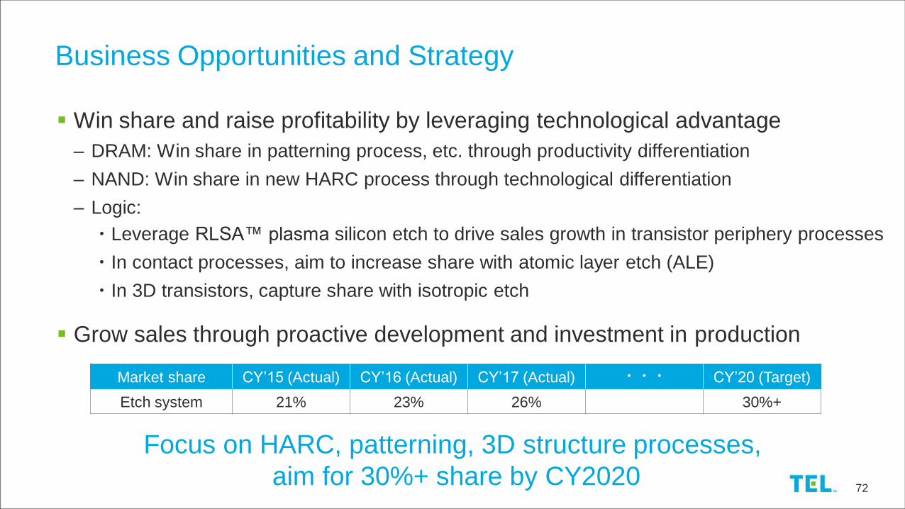
Win share and raise profitability by leveraging technological advantage
– DRAM: Win share in patterning process, etc. through productivity differentiation
– NAND: Win share in new HARC process through technological differentiation
– Logic:
・Leverage RLSA™ plasma silicon etch to drive sales growth in transistor periphery processes
・In contact processes, aim to increase share with atomic layer etch (ALE)
・In 3D transistors, capture share with isotropic etch
Grow sales through proactive development and investment in production
Business Opportunities and Strategy
Market share CY’15 (Actual) CY’16 (Actual) CY’17 (Actual) ・・・ CY’20 (Target)
Etch system 21% 23% 26% 30%+
Focus on HARC, patterning, 3D structure processes,
aim for 30%+ share by CY2020

CORP IR / May 29, 2018 73
Differentiate with technology related to
process accuracy, grew share in 6X/9X
generations, and aim to capture additional
processes in 12X
Capacitor process (HARC)
Copper interconnects
process: Leveraged
knowledge of logic
to win share
Patterning: Realized
reduced costs for
customers by combining etch steps
Memory: Results and Initiatives
Word line
isolation (slit)
Channel
(Memory hole)
Multi-level
contact
3D NAND HARC processDRAM
Simplify process
Capacitor
Interconnects
CY’18 CY’19 CY’20
6X/9X 9X 9X/12X
DRAM: Won share in target areas, doubling share from 3 years agoNAND: Won application from second customer in slit process.
Aim to leverage new technology to increase POR wins
CORP IR / May 29, 2018 74
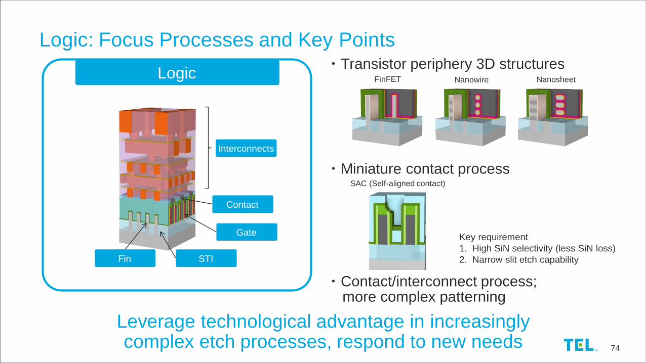
Logic: Focus Processes and Key Points
Logic
Contact
Interconnects
Gate
Fin
・Transistor periphery 3D structuresNanowire NanosheetFinFET
・Miniature contact process
Key requirement
1. High SiN selectivity (less SiN loss)
2. Narrow slit etch capability
・Contact/interconnect process; more complex patterning
SAC (Self-aligned contact)
STI
Leverage technological advantage in increasingly complex etch processes, respond to new needs

CORP IR / May 29, 2018 75
Leading-edge Logic Initiative 1: Silicon Etch
プラズマエッチング装置
Tactras™ RLSA™
Typical ICP
etcher
RLSA™ plasma
etcher
RLSA™ plasma BB
Pro
ce
ss P
erf
orm
an
ce
Stability and Productivity
Optimized Microwave
Conventional
Microwave
Adoption of
new technology
Superior aspects of RLSA™ plasma etcher
in silicon etch
Faceting
Depth variation
Non-vertical form
Equal depth
Vertical shape
RectangleFin Gate
In silicon etch, differentiate through processing performance and productivity
Transistor periphery 3D structures

CORP IR / May 29, 2018 76
Conventional etch Quasi-ALE*
Self-a
ligned
co
nta
ct
Si-A
RC
etc
h
Leading-edge Logic Initiative 2: Highly Selective Etch
SiN
SiO2
SiN
Si
-ARC
Desorption
Initial
SiO2
Adsorption
FC film
Activation
Ar + + +
Concept of Quasi-ALE
Aim to win share through rising demand for highly selective etch
*ALE (Atomic layer etch): Highly selective etch technology at the atomic level

CORP IR / May 29, 2018 77
Leading-edge Logic Initiative 3: Gas Chemical Etch
Si SiGeSi
N+3N+2N+1
SiGeMin. Fin pitch Min. Fin pitch Min. Fin pitch
Broadening of applications for gas chemical etch
Nanowire Nanosheet
Isotropic
SiGe etch
Post dummy Si removal Post gate oxide removal Post SiGe removal
Si/SiGe layer stack Si nanowire
Isotropic
Ox etch
Footing
Gas chemical etch
Wet etch
No footing
Differentiate through isotropic selective etch technology needed for 3D transistors
CORP IR / May 29, 2018 78
Miyagi Plant: New Logistics Building and Module Assembly and Shipping, New Development Building
Module: VTM**
Production start: Sep. 2018
Receiving Automatic
sorting
Automatic
shipping
New development building
Scheduled completion: Sep. 2018
Total floor space: 11,700m2
New Logistics
Building
Module: EFEM*
Production start: Jan. 2018
* VTM (Vacuum transfer module): Module that sends wafers to etch chamber
** EFEM (Equipment front end module): Module that moves wafers from FOUP/load ports to VTM

CORP IR / May 29, 2018 79
Expect continued growth in the etch system market driven by multi-layering of
3D NAND and increasing complexity in logic patterning
Aim to raise profitability by focusing on TEL’s strengths in HARC, patterning,
interconnects, achieving share of 30%+ in CY’20 through technological
differentiation
We will proactively invest towards further market growth
Summary
CORP IR / May 29, 2018 80
May 29, 2018
Shingo Tada
VP & GM, General Manager, Thin Film Formation BU
Deposition System Business Strategy
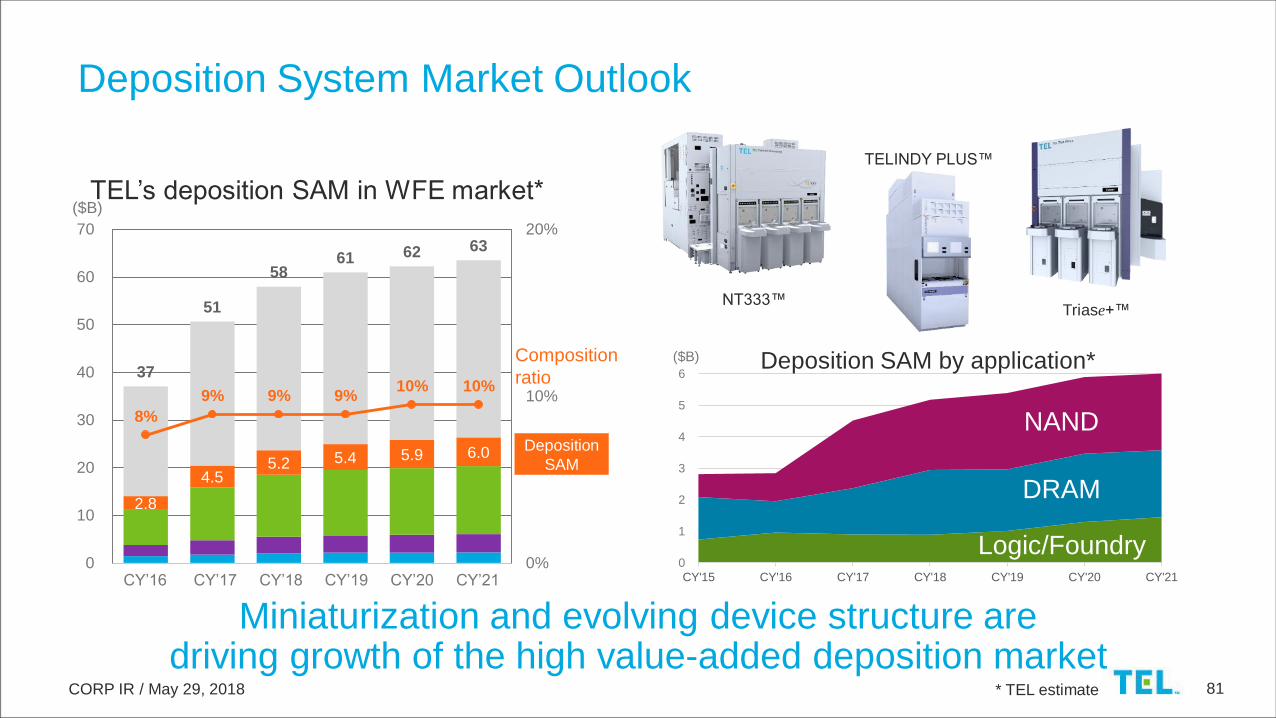
CORP IR / May 29, 2018 81
0
1
2
3
4
5
6
CY'15 CY'16 CY'17 CY'18 CY'19 CY'20 CY'21
Deposition System Market Outlook
Miniaturization and evolving device structure are driving growth of the high value-added deposition market
2.8
4.55.2 5.4 5.9 6.0
37
51
58 61 62 63
8%
9% 9% 9%10% 10%
0%
10%
20%
0
10
20
30
40
50
60
70
2016 2017 2018 2019 2020 2021
($B)
Deposition
SAM
Composition
ratio
TEL’s deposition SAM in WFE market*
NT333™
TELINDY PLUS™
Triase+™
* TEL estimate
NAND
DRAM
Logic/Foundry
($B) Deposition SAM by application*
CY’16 CY’17 CY’18 CY’19 CY’20 CY’21
CORP IR / May 29, 2018 82
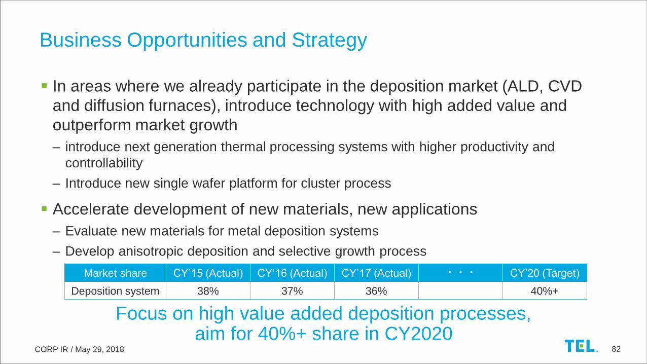
In areas where we already participate in the deposition market (ALD, CVD
and diffusion furnaces), introduce technology with high added value and
outperform market growth
– introduce next generation thermal processing systems with higher productivity and
controllability
– Introduce new single wafer platform for cluster process
Accelerate development of new materials, new applications
– Evaluate new materials for metal deposition systems
– Develop anisotropic deposition and selective growth process
Business Opportunities and Strategy
Market share CY’15 (Actual) CY’16 (Actual) CY’17 (Actual) ・・・ CY’20 (Target)
Deposition system 38% 37% 36% 40%+
Focus on high value added deposition processes, aim for 40%+ share in CY2020

CORP IR / May 29, 2018 83
CY'14 CY'15 CY'16 CY'17 CY'18 CY'19 CY'20
In semi-batch systems, make high quality film
required for miniaturization and shift to 3D
structure, and raise productivity
Approach to Deposition Market
CVD systemALD system
Use our huge productivity advantage in batch
systems to differentiate in memory
Achieve high quality metal deposition to
enable further miniaturization
Aim to grow profit through and new technology for further miniaturization and next-generation semiconductors
ALD system market
CAGR >15%
TEL estimate
¥90.0B
¥210.0B
Batch system
TELINDY PLUS™
Metal deposition system
Triase+™
Semi-batch ALD system
NT333™
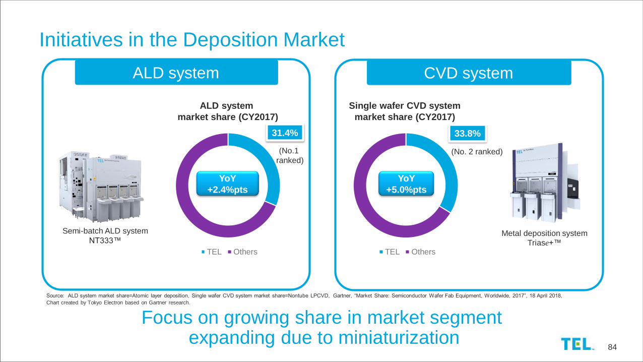
CORP IR / May 29, 2018 84
Initiatives in the Deposition Market
CVD systemALD system
Metal deposition system
Triase+™
Semi-batch ALD system
NT333™
列1
TEL Others
ALD system
market share (CY2017)
31.4%
YoY
+2.4%pts
列1
TEL Others
Single wafer CVD system
market share (CY2017)
YoY
+5.0%pts
33.8%
(No.1
ranked)(No. 2 ranked)
Source: ALD system market share=Atomic layer deposition, Single wafer CVD system market share=Nontube LPCVD, Gartner, “Market Share: Semiconductor Wafer Fab Equipment, Worldwide, 2017”, 18 April 2018,
Chart created by Tokyo Electron based on Gartner research.
Focus on growing share in market segmentexpanding due to miniaturization

CORP IR / May 29, 2018 85
2.26 2.22
2.09
2.22
2.00
2.10
2.20
2.30
2.40
Thermaloxide
furnace @1000 deg.C
DCS-HTOfurnace @780 deg.C
ThermalALD oxideNT333 @400 deg.C
HQ oxideNT333 @400 deg.C
film
density (
g/c
m3)
high temp.high temp.
low temp.low temp.
Oxidation area
Source area
Dielectric Film Deposition Technology for High Aspect Ratio StructureHigh-k dielectric film High-k dielectric filmDRAM 3D NAND Block oxide film
Charge trap film
Tunnel oxide film
Protective oxide
Gas injection
directly above wafer
High productivity semi-batch ALD
Film density
ALD for high-k dielectric film
ALD for high quality oxide film
#5
Isolation by N2
O3
Metal precursor
N2
N2
Si precursor
Oxidation
Modification
Realized high productivity deposition technology that forms high quality, uniform dielectric film without pattern dependence
Isolation by N2

CORP IR / May 29, 2018 86
Metal Deposition Technology for High Aspect Ratio
Bottom electrode deposition Upper electrode deposition Word line, contact barrier depositionDRAM 3D NAND
High throughput
Uniformity
ASFD:Advanced sequential flow deposition Φ30 nm
Aspect ratio = 40:1
Non-uniformity
< 1.0% @ 1 sigma
Step coverage
> 90%
Optimized deposition chamber design for ASFD provideshigh performance and high productivity
Minimizes chamber volume
High speed, high concentration gas
injection system
Symmetrical gas flow design

CORP IR / May 29, 2018 87
Next generation thermal processing system
– Introduce SLB* product with high productivity and efficiency
– Adoption of new, high precision controller will contribute to enhance tool matching and increasing uptime
New single wafer platform
– Smaller footprint, higher productivity
– Enables diverse cluster processes
Deposition Systems: Striving for Further Growth
New platform
Diagnostic
* SLB: Super large batch
Tool
Matching
Optimum
Control
New platform
Expand market share in areas where we already participate in by increasing productivity and responding to diverse process needs

CORP IR / May 29, 2018 88
Evaluation of new materials
for metal deposition systems
– Achieve low resistance with
thin wire
– Excellent gap fill capabilities
Develop anisotropic deposition and
selective deposition
– Achieving gap fill and bottom up processes
by using TEL’s unique deposition
technique
Deposition Systems:Initiatives Towards New Materials and Applications
TEL/TEL TEL/TEL
Ge(SiGe)
AR: ~ 5:1
CD: 40nm
Depth 200nm
0 5 10 15 20 25
Resis
tivity[u
oh
m c
m]
Thickness[nm]
TiN/Convetional W
TiN/ FFW
TiN/New Material
Gap fill Bottom up
SiO2
AR: 8:1
CD: 43nm
Depth 331nm
Resistivity ratio at thin film
Film formation
in processing
After
formation
Expanding SAM through the development of new applications for miniaturization

CORP IR / May 29, 2018 89
Augmenting Production System
• Construction start (scheduled): October 2018
• Completion (scheduled):
September 2019 (First phase)
December 2020 (Second phase)
• Products: Thermal processing systems
• Construction start (scheduled): January 2019
• Completion (scheduled): April 2020
• Products: Single wafer deposition, gas
chemical etch, and test systems
New building at Tohoku PlantNew building at Yamanashi (Fujii) Plant
Expand production system, flexibly respond to future growth in demand
CORP IR / May 29, 2018 90
Deposition market continues to expand, especially in memory
Expand our market share in the fields of ALD, single wafer CVD and thermal
processing systems, by raising the competitiveness of our existing products
and introducing new products
Start construction of new factory buildings in FY2019, increase production
capacity for sustainable growth
Summary

CORP IR / May 29, 2018 91
May 29, 2018
Tsuguhiko Matsuura
VP & GM, General Manager, FPD BU
FPD Business Strategy
CORP IR / May 29, 2018 92
-10%
-5%
0%
5%
10%
15%
20%
25%
0
20
40
60
80
100
120
FY'15 FY'16 FY'17 FY'18 FY'19 FY'21
Sales Operating margin
0
5
10
15
20
25
CY'15 CY'16 CY'17 CY'18 CY'19 CY'20
Coater/developer Dry etch TFT others
AMOLED CF, Cell, Others
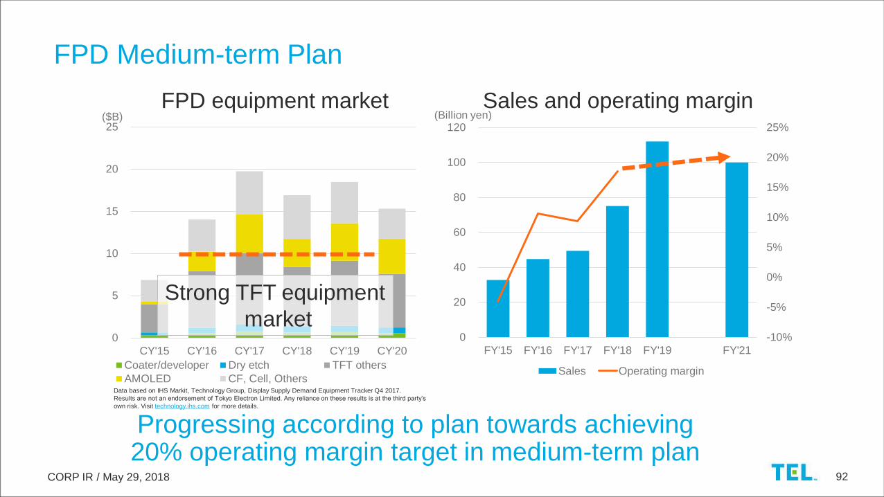
FPD Medium-term Plan
Progressing according to plan towards achieving 20% operating margin target in medium-term plan
($B)
Strong TFT equipment
market
FPD equipment market Sales and operating margin(Billion yen)
Data based on IHS Markit, Technology Group, Display Supply Demand Equipment Tracker Q4 2017.
Results are not an endorsement of Tokyo Electron Limited. Any reliance on these results is at the third party’s
own risk. Visit technology.ihs.com for more details.

CORP IR / May 29, 2018 93
Established our leading position in G10.5
Introduced new Betelex™ platform etch system
Expansion of PICP™* etch system going well
Medium-term Plan Progress: Highlights
FPD coater/developer
ExcelinerTM
FPD plasma etch/ash system
ImpressioTM
FPD plasma etch/ash system
BetelexTM
* PICP: Plasma source for producing extremely uniform high density plasma on substrate

CORP IR / May 29, 2018 94
Display Trends
Technological change in displays increasing business opportunities
Increasing screen size
Increasing resolution
FHD 4K 8K
OLED
LCD OLED
TFT
Color filter
Backlight
LCD
TFT
Emissive
layer
Flexible, edge bent, free format
TV
Mobile, VR 300 ppi 1000 ppi
Design flexibility

CORP IR / May 29, 2018 95
Data based on IHS Markit, Technology Group, Display Supply Demand Equipment Tracker Q4 2017.
Results are not an endorsement of Tokyo Electron Limited. Any reliance on these results is at the third
party’s own risk. Visit technology.ihs.com for more details.
Greater-than-expected growth in investment
Maintain high market share through technological differentiation (large area
plasma control, air floating coater)
0
5
10
15
20
CY'16 CY'17 CY'18 CY'19 CY'20
Business Opportunity: G10.5 Equipment Market
Eight 65 inch TV panel substrate possible
“65
3,3
70
mm
2,940 mm
G10.5 TFT array equipment market($B)
Increased sales far beyond market growth bymeeting customers’ technological needs

CORP IR / May 29, 2018 96
Business Opportunity: Metal Oxide/LTPS
TFT array a-Si Metal Oxide LTPS
Representation
of structure
ApplicationLCD TV
Monitor
OLED TV
Tablet
Smartphone
(LCD/OLED)
Number of
masks5 6-8 9-13
Dry etch
processes
3
a-Si, SiNx
3
SiO, SiNx
~11
SiO, metal
Flexible displays
+2 processes
OLED process
(G6 Half Size)+3-4 processes
Further new
needs
Number of etch processes increased as more advanced technology sought

CORP IR / May 29, 2018 97
Material utilization significantly more efficient than current evaporation method
Companies improving functionality of ink
Business Opportunity: Growth of OLED TV Market
OLED TV(K units)
Inkjet printing system for manufacturing OLED planes
EliusTM 2500
Differentiate with inkjet printing systemtowards growth in the OLED TV market
0
2,000
4,000
6,000
8,000
CY'16 CY'17 CY'18 CY'19 CY'20 CY'21Data based on IHS Markit, Technology Group, Display Long-Term Demand Forecast
Tracker Q4 2017. Results are not an endorsement of Tokyo Electron Limited. Any
reliance on these results is at the third party’s own risk. Visit technology.ihs.com for
more details.

CORP IR / May 29, 2018 98
Increase share and profitability in growing market, business
progressing according to plan
New medium-term plan FY2021 target: sales ¥100.0B, operating
margin over 20%
For leading-edge production processes, focus on areas where we
have technological superiority
– High performance PICP™ etch system
– Etch system and coater/developer for G10.5 substrate
– Inkjet printing system for OLED TVs
Summary
CORP IR / May 29, 2018 99


