DEGGENDORF INSTITUTE of TECHNOLOGY, GERMANY
Prof. Dr. Werner Frammelsberger –
Mechanical Engineering & Mechantronics
Micro- and Nano-Analytics Research Team
Atomic Force Microscopy –
Characteristics and Advanced Applications
Prof. Dr. Werner Frammelsberger Mechanical Engineering & Mechatronics
Micro- and Nano-Analytics
Research Team
Agenda
• Micro- and Nano-Analytics Research Team
• Introduction
• Atomic Force Microscope (AFM) – Principles and Fundamental Applications
• Conductive AFM (C-AFM), Tunnelling AFM (Tuna)
• Scanning Capacitance Microscopy (SCM) Techniques
• Kelvin Probe Force Microscopy (KPFM) Techniques
• Summary
• What's next?
03.11.2013 Fakultät Maschinenbau und Mechatronik, Prof. Dr. Werner Frammelsberger 3
Micro and Nano-Analytics – Basics
• Founded in 2000 by Prof Dr. Günther Benstetter
• Hosted at Faculty of Electrical Engineering & Media Technology http://www.hdu-deggendorf.de/de/fakultaeten/et-mt/forschungsteams/1300-mikro-und-nanoanalytik
03.11.2013 Prof. Dr. Werner Frammelsberger, www.dit.edu 4
Intention
• Concentration on complex and innovative analysis methods that require high-level expertise
• Competent service and development partner for regional and superregional economy and industry, predominantly SEMs
• Basis for various academic activities at Bachelor, Master and PhD level
Concept – three main steps
• Development of basic analysis principles and analysis methods with international universities and research institutions and in with participation of industrial partners from SMEs..
• Application centred optimisation of methods and techniques – accompanied with associated numerical simulations
• Customised analysis and measurement services
SME: Small and Medium-Sized Enterprises
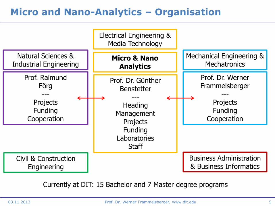
Micro and Nano-Analytics – Organisation
03.11.2013 Prof. Dr. Werner Frammelsberger, www.dit.edu 5
Civil & Construction Engineering
Business Administration & Business Informatics
Electrical Engineering & Media Technology
Mechanical Engineering & Mechatronics
Natural Sciences & Industrial Engineering
Prof. Dr. Günther Benstetter
--- Heading
Management Projects Funding
Laboratories Staff
Prof. Raimund Förg ---
Projects Funding
Cooperation
Prof. Dr. Werner Frammelsberger
--- Projects Funding
Cooperation
Micro & Nano Analytics
Currently at DIT: 15 Bachelor and 7 Master degree programs
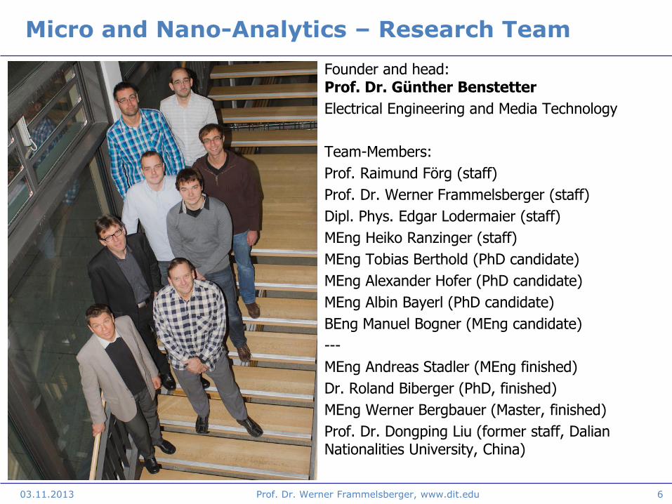
Micro and Nano-Analytics – Research Team
Founder and head: Prof. Dr. Günther Benstetter
Electrical Engineering and Media Technology
Team-Members:
Prof. Raimund Förg (staff)
Prof. Dr. Werner Frammelsberger (staff)
Dipl. Phys. Edgar Lodermaier (staff)
MEng Heiko Ranzinger (staff)
MEng Tobias Berthold (PhD candidate)
MEng Alexander Hofer (PhD candidate)
MEng Albin Bayerl (PhD candidate)
BEng Manuel Bogner (MEng candidate)
---
MEng Andreas Stadler (MEng finished)
Dr. Roland Biberger (PhD, finished)
MEng Werner Bergbauer (Master, finished)
Prof. Dr. Dongping Liu (former staff, Dalian Nationalities University, China)
03.11.2013 6 Prof. Dr. Werner Frammelsberger, www.dit.edu
Micro and Nano-Analytics – Activities, Services
Application and services include:
• Manufacturing associated quality assurance, reliability and failure analysis
• System characterizations: Failure, construction and reliability analysis in electronic and optoelectronic devices and systems
• Basic material characterization (defects, contamination, physical properties, organic and inorganic materials)
• Surface and thin film characterization (roughness analysis, investigations of surface properties including abrasion and scratch resistance)
• …
03.11.2013 Prof. Dr. Werner Frammelsberger, www.dit.edu 7
Academic Activities:
• Bachelor and Master Lectures, student projects, hands on training, internships, theses, academic supervision
• Master Applied Research (joint project) http://www.forschungsmaster.de/
Projects, lectures, administration, management, academic supervision
• PhD studies and research projects Funding, management, administration, academic supervision
• Applied research
– in cooperation with German and international Universities and Universities of Applied Sciences and
– Numerous German and international corporate partners
Micro and Nano-Analytics – Key Equipment and Methods
• Scanning electron microscopy (SEM) based methods including: Energy dispersive X-ray spectroscopy (EDX), Wavelength-dispersive X-ray spectroscopy (WDX), Electron backscatter diffraction (EBSD), Micro X-ray fluorescence spectroscopy (μXRF), Scanning Transmission Electron Microscopy (STEM)
• Scanning probe microscopy (SPM) based methods including: Scanning capacitance microscopy (SCM) and spectroscopy (SCS), Tunnelling current microscopy (C-AFM, TUNA), Scanning Spreading Resistance Microscopy (SSRM), Kelvin Probe Force Microscopy (KPFM), Electric Force Microscopy (EFM), Magnetic Force Microscopy (MFM), Nano-scratch and wear tests, Thermal scanning probe microscopy (ThSPM)
• Additional and supporting equipment and units: Fourier Transformation Spectroscope (FT-IR), plasma cleaner/coater, wafer prober, sample preparation lab and optical microscopy…
03.11.2013 Prof. Dr. Werner Frammelsberger, www.dit.edu 8
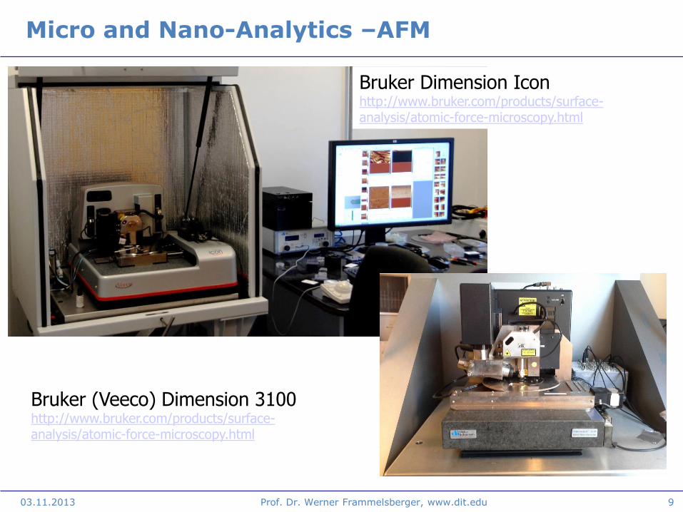
Micro and Nano-Analytics –AFM
03.11.2013 Prof. Dr. Werner Frammelsberger, www.dit.edu 9
Bruker (Veeco) Dimension 3100 http://www.bruker.com/products/surface-analysis/atomic-force-microscopy.html
Bruker Dimension Icon http://www.bruker.com/products/surface-analysis/atomic-force-microscopy.html
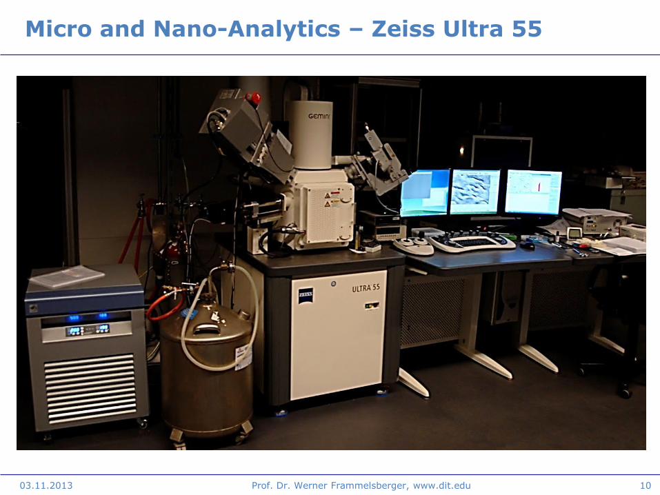
Micro and Nano-Analytics – Zeiss Ultra 55
03.11.2013 Prof. Dr. Werner Frammelsberger, www.dit.edu 10
03.11.2013 Prof. Dr. Werner Frammelsberger, www.dit.edu 11
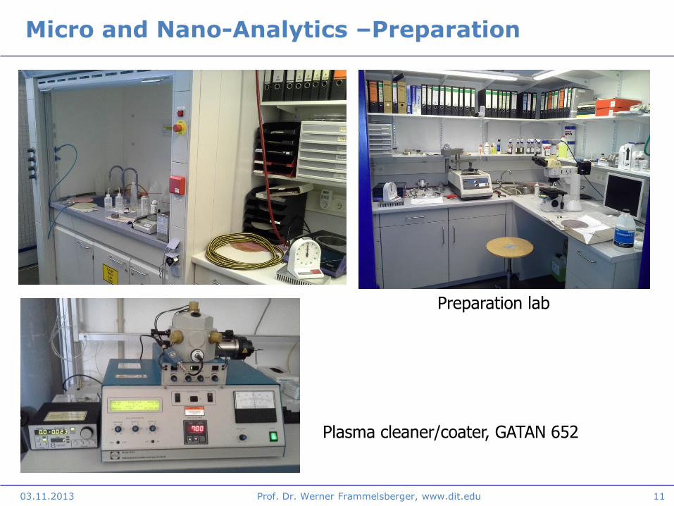
Micro and Nano-Analytics –Preparation
Preparation lab
Plasma cleaner/coater, GATAN 652
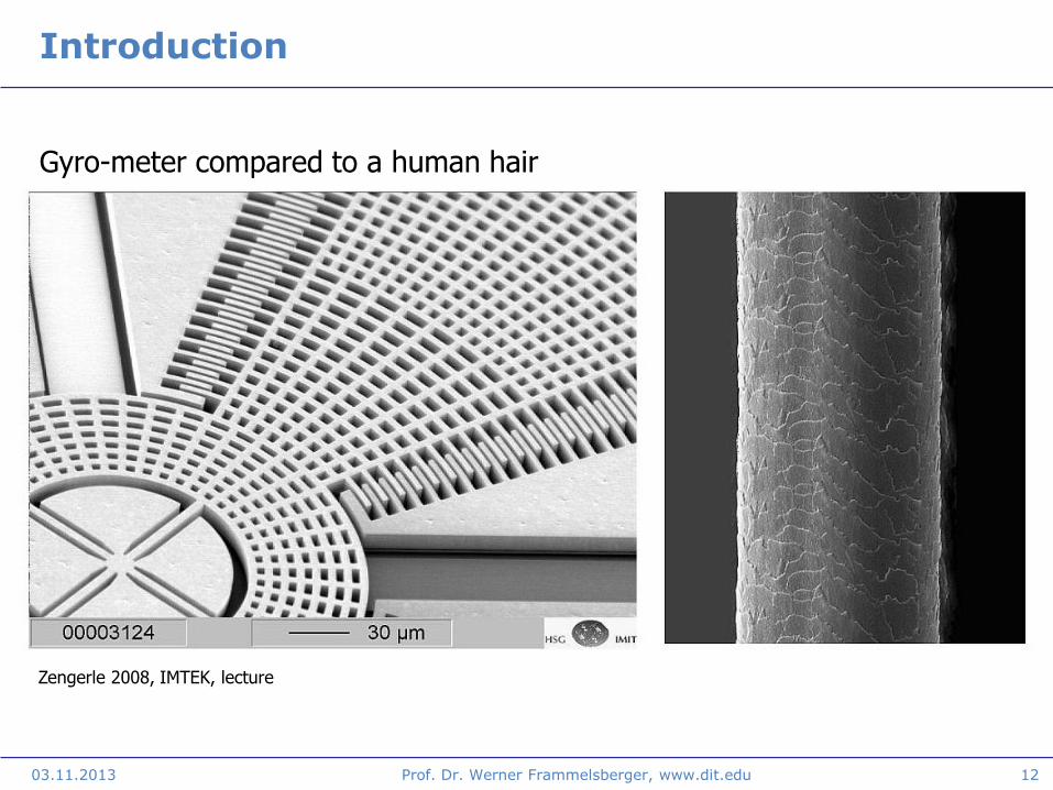
Introduction
03.11.2013 12
Gyro-meter compared to a human hair
Zengerle 2008, IMTEK, lecture
Prof. Dr. Werner Frammelsberger, www.dit.edu
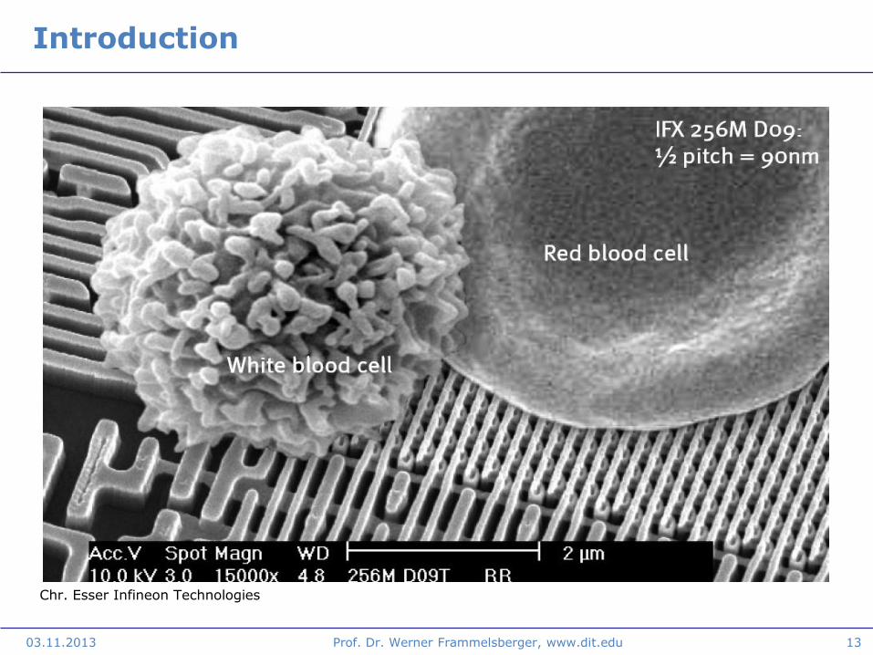
Introduction
03.11.2013 13
Chr. Esser Infineon Technologies
Prof. Dr. Werner Frammelsberger, www.dit.edu
Introduction
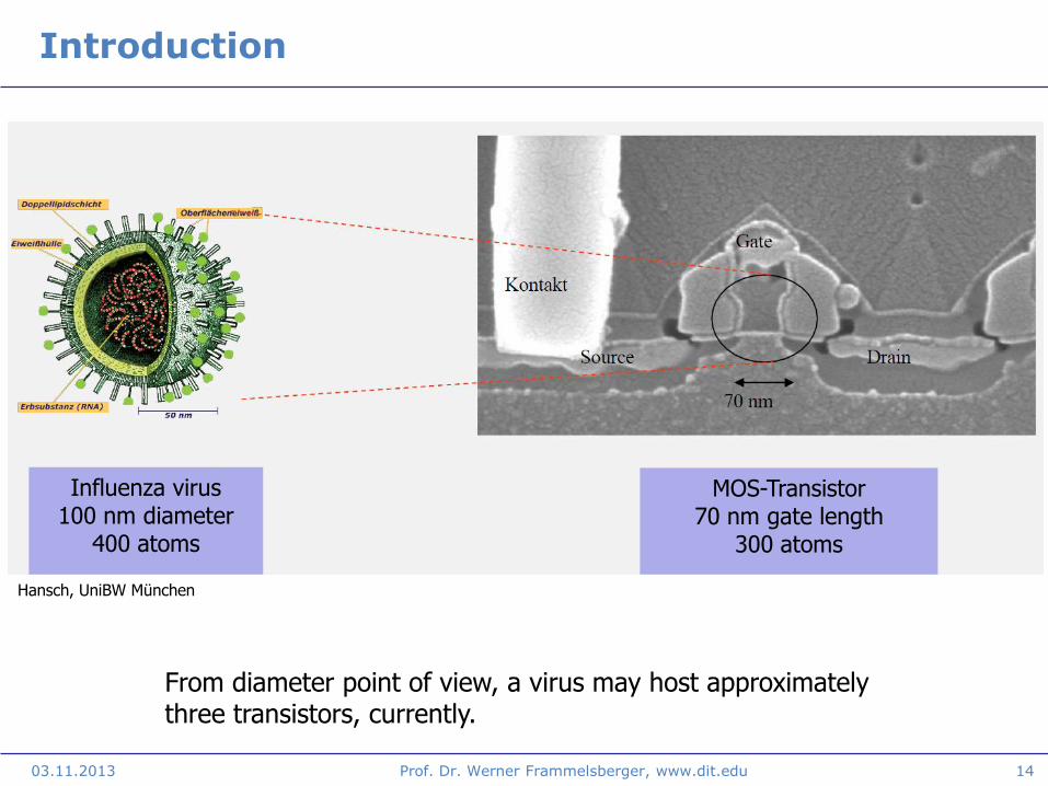
03.11.2013 14
Hansch, UniBW München
From diameter point of view, a virus may host approximately three transistors, currently.
Influenza virus 100 nm diameter
400 atoms
MOS-Transistor 70 nm gate length
300 atoms
Prof. Dr. Werner Frammelsberger, www.dit.edu
Introduction
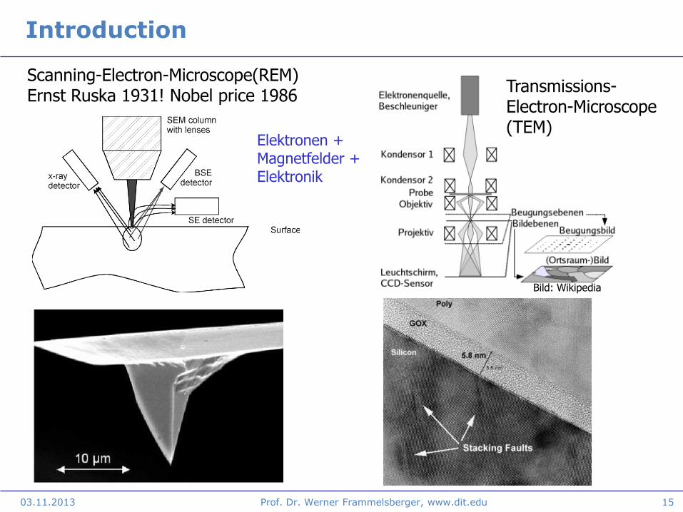
03.11.2013 15
Scanning-Electron-Microscope(REM) Ernst Ruska 1931! Nobel price 1986
Bild: Wikipedia
Transmissions-Electron-Microscope (TEM)
Elektronen + Magnetfelder + Elektronik
Prof. Dr. Werner Frammelsberger, www.dit.edu
Introduction
• High resolution imaging of micro and nanostructures with SEM possible
• Content analysis with SEM based techniques (EDX, WDX…) possible, however:
– Conductive specimen necessary
– Limited 3D-imaging
– No liquid specimen possible
– Limited information from thin films
– No information about mechanical properties
– No information about electrical properties
– No high resolution chemical/physical analysis
• Alternative analysis techniques necessary
03.11.2013 16 Prof. Dr. Werner Frammelsberger, www.dit.edu
17
Atomic Force Microscope – Principles
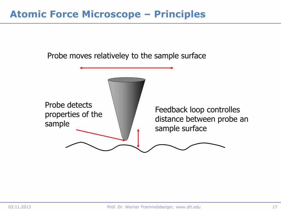
Probe moves relativeley to the sample surface
Probe detects properties of the sample
Feedback loop controlles distance between probe an sample surface
03.11.2013 Prof. Dr. Werner Frammelsberger, www.dit.edu
Atomic Force Microscope – Principles
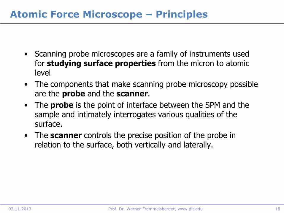
• Scanning probe microscopes are a family of instruments used for studying surface properties from the micron to atomic level
• The components that make scanning probe microscopy possible are the probe and the scanner.
• The probe is the point of interface between the SPM and the sample and intimately interrogates various qualities of the surface.
• The scanner controls the precise position of the probe in relation to the surface, both vertically and laterally.
18 03.11.2013 Prof. Dr. Werner Frammelsberger, www.dit.edu
19
Atomic Force Microscope – Principles
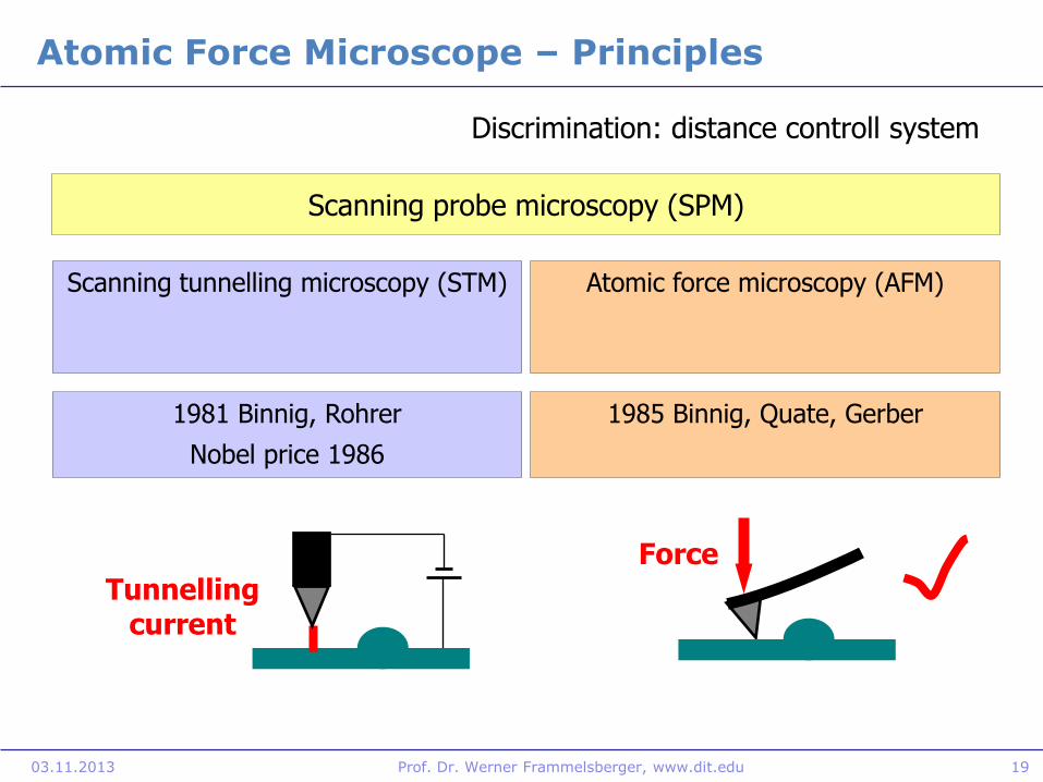
Scanning probe microscopy (SPM)
Scanning tunnelling microscopy (STM) Atomic force microscopy (AFM)
1981 Binnig, Rohrer
Nobel price 1986
1985 Binnig, Quate, Gerber
Force
Tunnelling current
Discrimination: distance controll system
03.11.2013 Prof. Dr. Werner Frammelsberger, www.dit.edu
20
Atomic Force Microscope – Principles
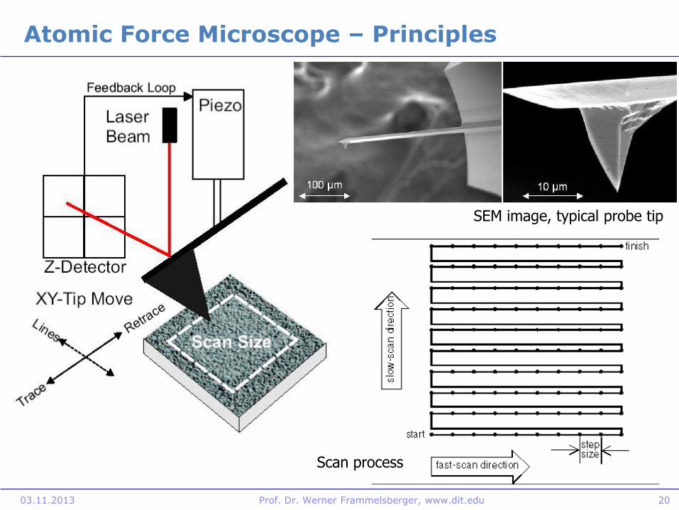
SEM image, typical probe tip
Scan process
03.11.2013 Prof. Dr. Werner Frammelsberger, www.dit.edu
21
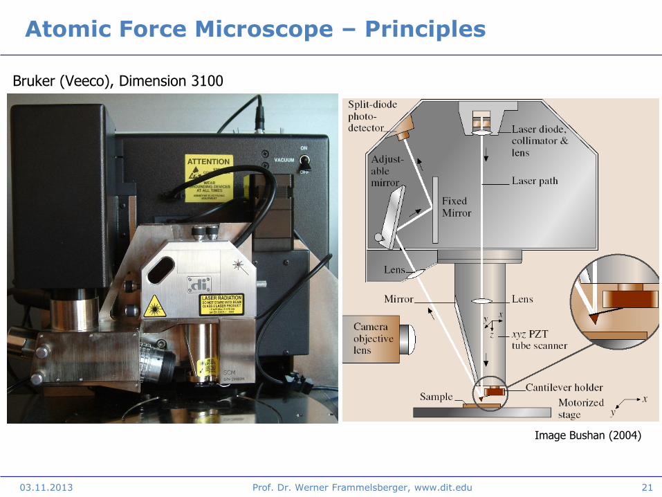
Atomic Force Microscope – Principles
Image Bushan (2004)
Bruker (Veeco), Dimension 3100
03.11.2013 Prof. Dr. Werner Frammelsberger, www.dit.edu
22
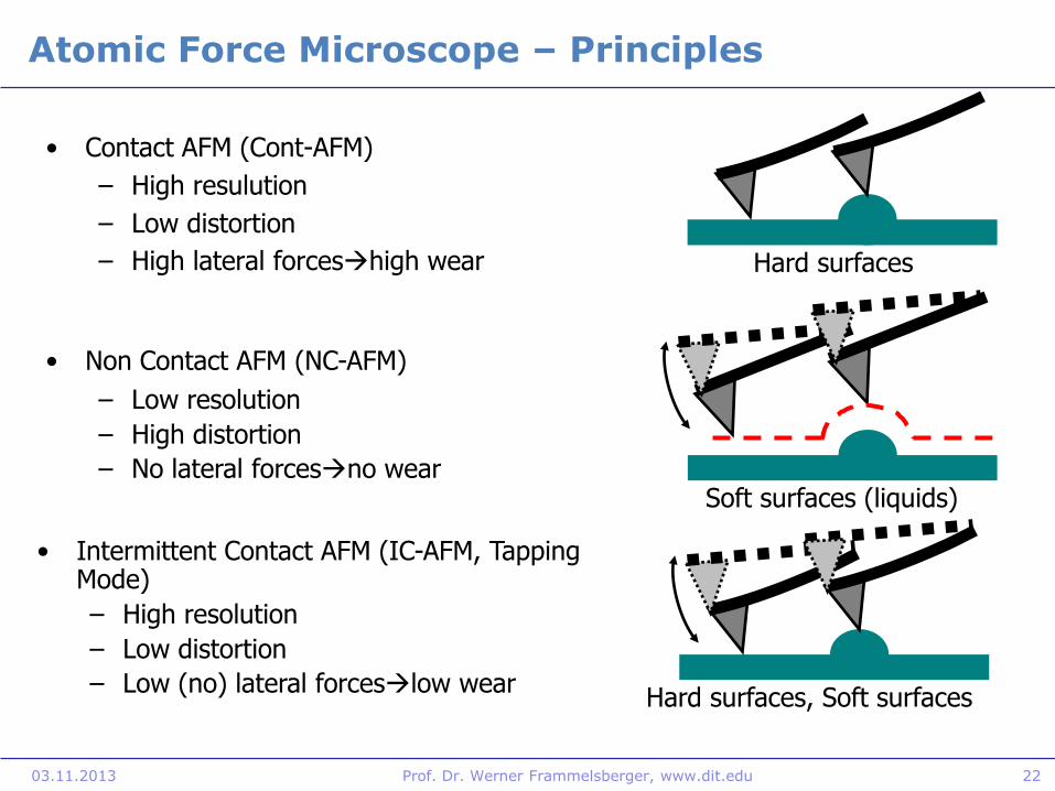
Atomic Force Microscope – Principles
• Contact AFM (Cont-AFM)
– High resulution
– Low distortion
– High lateral forceshigh wear
• Non Contact AFM (NC-AFM)
– Low resolution
– High distortion
– No lateral forcesno wear
Hard surfaces
Soft surfaces (liquids)
Hard surfaces, Soft surfaces
• Intermittent Contact AFM (IC-AFM, Tapping Mode)
– High resolution
– Low distortion
– Low (no) lateral forceslow wear
03.11.2013 Prof. Dr. Werner Frammelsberger, www.dit.edu
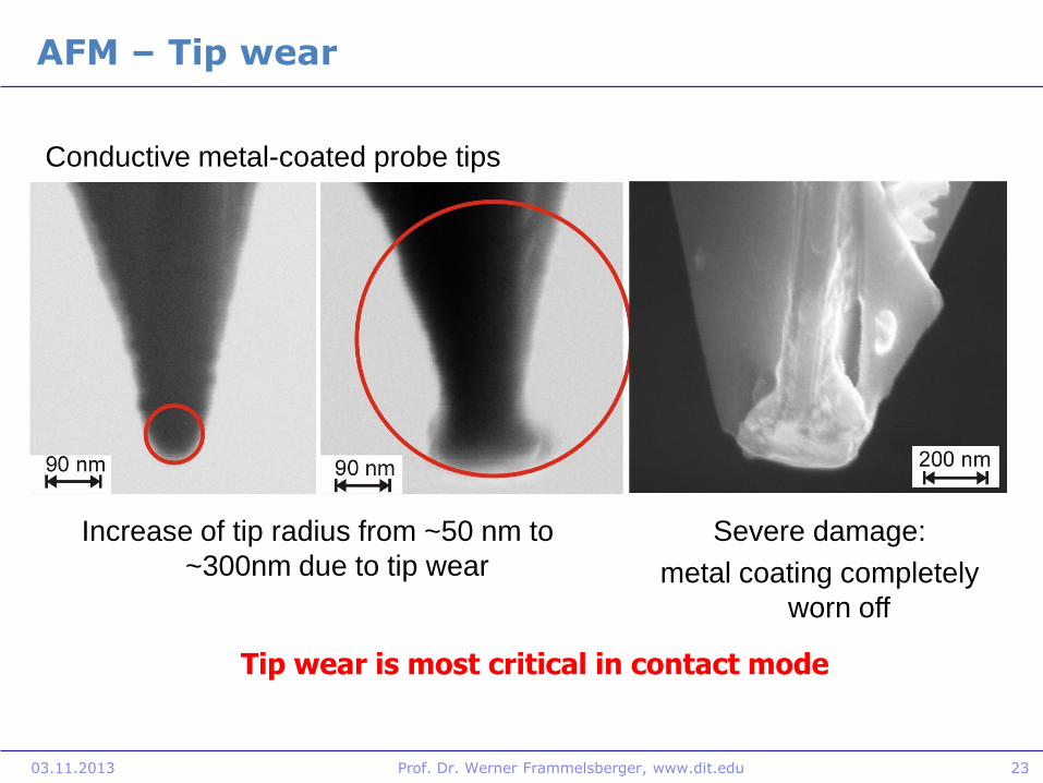
AFM – Tip wear
23
Increase of tip radius from ~50 nm to
~300nm due to tip wear
Severe damage:
metal coating completely
worn off
Conductive metal-coated probe tips
Tip wear is most critical in contact mode
03.11.2013 Prof. Dr. Werner Frammelsberger, www.dit.edu
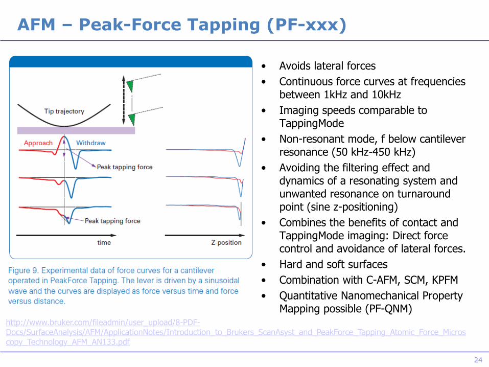
AFM – Peak-Force Tapping (PF-xxx)
• Avoids lateral forces
• Continuous force curves at frequencies between 1kHz and 10kHz
• Imaging speeds comparable to TappingMode
• Non-resonant mode, f below cantilever resonance (50 kHz-450 kHz)
• Avoiding the filtering effect and dynamics of a resonating system and unwanted resonance on turnaround point (sine z-positioning)
• Combines the benefits of contact and TappingMode imaging: Direct force control and avoidance of lateral forces.
• Hard and soft surfaces
• Combination with C-AFM, SCM, KPFM
• Quantitative Nanomechanical Property Mapping possible (PF-QNM)
24
http://www.bruker.com/fileadmin/user_upload/8-PDF-Docs/SurfaceAnalysis/AFM/ApplicationNotes/Introduction_to_Brukers_ScanAsyst_and_PeakForce_Tapping_Atomic_Force_Microscopy_Technology_AFM_AN133.pdf
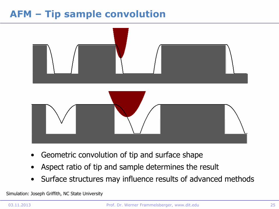
AFM – Tip sample convolution
Simulation: Joseph Griffith, NC State University
• Geometric convolution of tip and surface shape
• Aspect ratio of tip and sample determines the result
• Surface structures may influence results of advanced methods
25 03.11.2013 Prof. Dr. Werner Frammelsberger, www.dit.edu
26
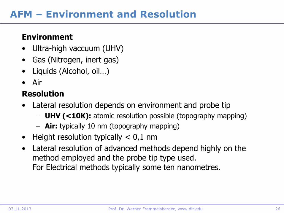
AFM – Environment and Resolution
Environment
• Ultra-high vaccuum (UHV)
• Gas (Nitrogen, inert gas)
• Liquids (Alcohol, oil…)
• Air
Resolution
• Lateral resolution depends on environment and probe tip
– UHV (<10K): atomic resolution possible (topography mapping)
– Air: typically 10 nm (topography mapping)
• Height resolution typically < 0,1 nm
• Lateral resolution of advanced methods depend highly on the method employed and the probe tip type used. For Electrical methods typically some ten nanometres.
03.11.2013 Prof. Dr. Werner Frammelsberger, www.dit.edu
27
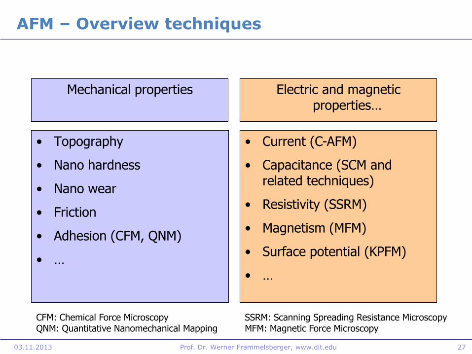
AFM – Overview techniques
• Topography
• Nano hardness
• Nano wear
• Friction
• Adhesion (CFM, QNM)
• …
• Current (C-AFM)
• Capacitance (SCM and related techniques)
• Resistivity (SSRM)
• Magnetism (MFM)
• Surface potential (KPFM)
• …
Electric and magnetic properties…
Mechanical properties
SSRM: Scanning Spreading Resistance Microscopy MFM: Magnetic Force Microscopy
CFM: Chemical Force Microscopy QNM: Quantitative Nanomechanical Mapping
03.11.2013 Prof. Dr. Werner Frammelsberger, www.dit.edu
28
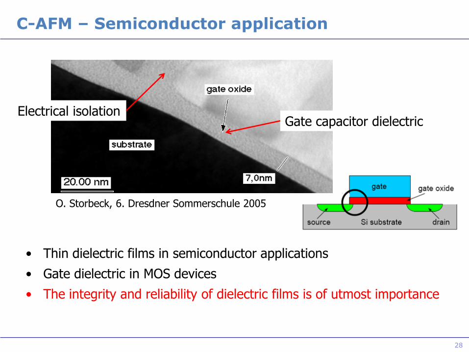
C-AFM – Semiconductor application
• Thin dielectric films in semiconductor applications
• Gate dielectric in MOS devices
• The integrity and reliability of dielectric films is of utmost importance
O. Storbeck, 6. Dresdner Sommerschule 2005
Electrical isolation Gate capacitor dielectric
29
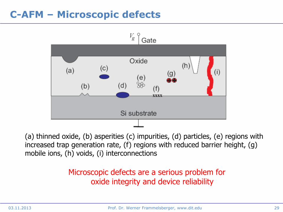
C-AFM – Microscopic defects
(a) thinned oxide, (b) asperities (c) impurities, (d) particles, (e) regions with increased trap generation rate, (f) regions with reduced barrier height, (g) mobile ions, (h) voids, (i) interconnections
Microscopic defects are a serious problem for oxide integrity and device reliability
03.11.2013 Prof. Dr. Werner Frammelsberger, www.dit.edu
30
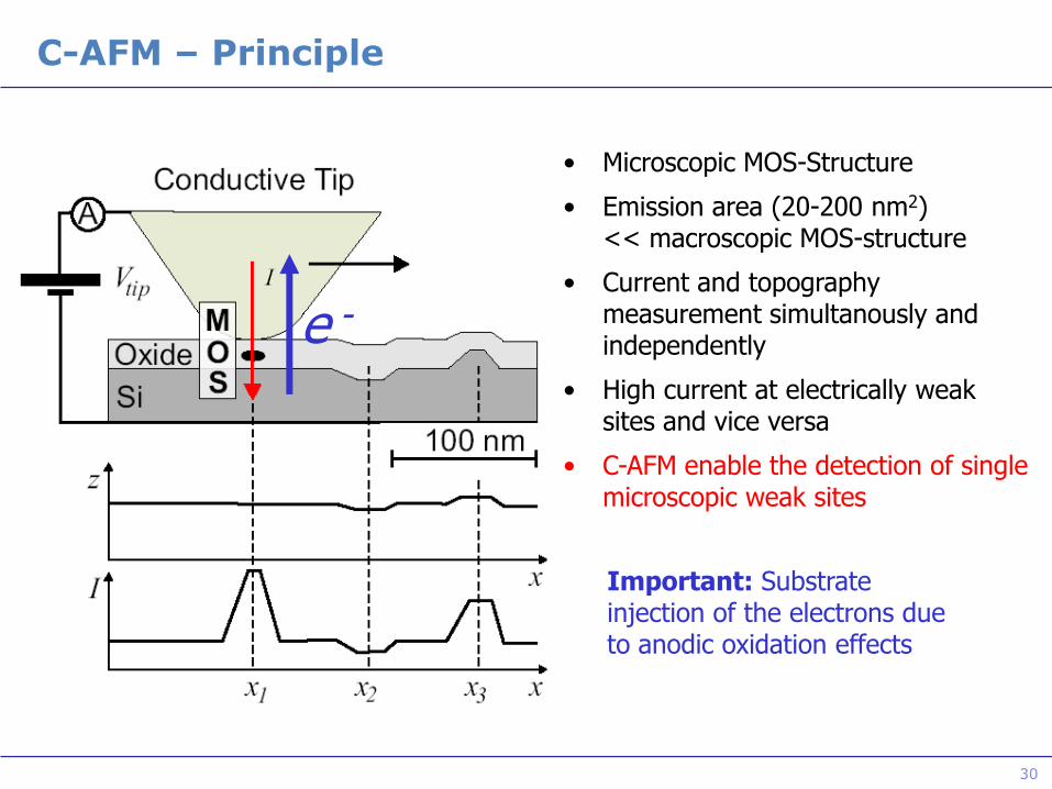
C-AFM – Principle
• Microscopic MOS-Structure
• Emission area (20-200 nm2) << macroscopic MOS-structure
• Current and topography measurement simultanously and independently
• High current at electrically weak sites and vice versa
• C-AFM enable the detection of single microscopic weak sites
e -
Important: Substrate injection of the electrons due to anodic oxidation effects
31
C-AFM – Microscopic vs. macroscopic
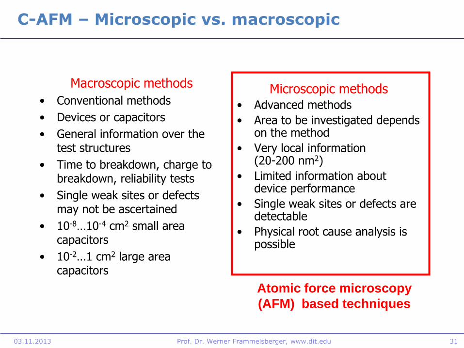
Macroscopic methods
• Conventional methods
• Devices or capacitors
• General information over the test structures
• Time to breakdown, charge to breakdown, reliability tests
• Single weak sites or defects may not be ascertained
• 10-8…10-4 cm2 small area capacitors
• 10-2…1 cm2 large area capacitors
Microscopic methods • Advanced methods
• Area to be investigated depends on the method
• Very local information (20-200 nm2)
• Limited information about device performance
• Single weak sites or defects are detectable
• Physical root cause analysis is possible
Atomic force microscopy
(AFM) based techniques
03.11.2013 Prof. Dr. Werner Frammelsberger, www.dit.edu
32
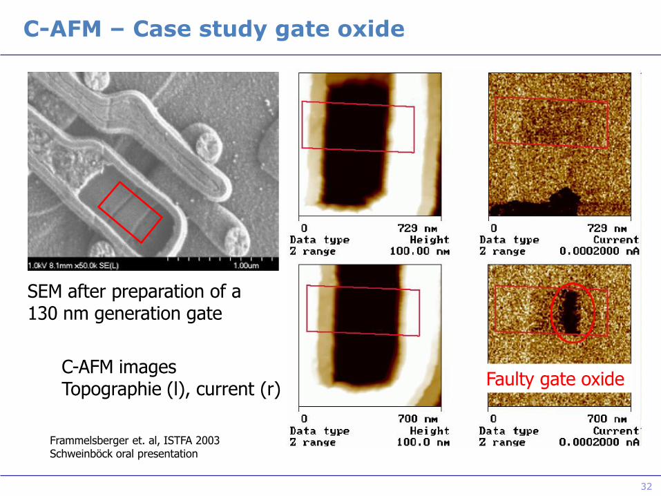
C-AFM – Case study gate oxide
Frammelsberger et. al, ISTFA 2003 Schweinböck oral presentation
C-AFM images Topographie (l), current (r)
SEM after preparation of a 130 nm generation gate
Faulty gate oxide
33
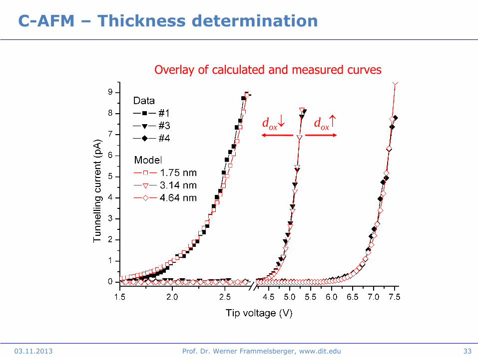
C-AFM – Thickness determination
Overlay of calculated and measured curves
dox dox
03.11.2013 Prof. Dr. Werner Frammelsberger, www.dit.edu
34
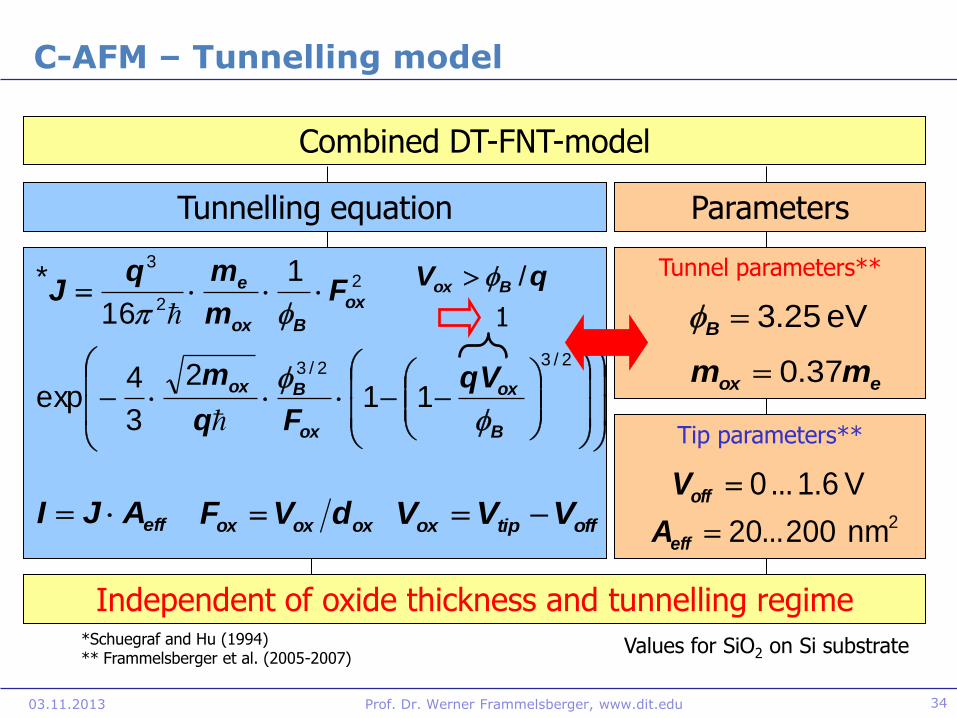
C-AFM – Tunnelling model
Combined DT-FNT-model
Tip parameters**
2nm 200...20effA
V6.1 ... 0offV
*Schuegraf and Hu (1994) ** Frammelsberger et al. (2005-2007)
Tunnel parameters**
eV 25.3B
eox mm 37.0
Parameters Tunnelling equation
Independent of oxide thickness and tunnelling regime
2/32/3
2
2
3
112
3
4exp
1
16
*
B
ox
ox
Box
ox
Box
e
qV
Fq
m
Fm
mqJ
oxoxox dVF offtipox VVV effAJI
qV Box /
1
Values for SiO2 on Si substrate
03.11.2013 Prof. Dr. Werner Frammelsberger, www.dit.edu
35
Tunnelling model
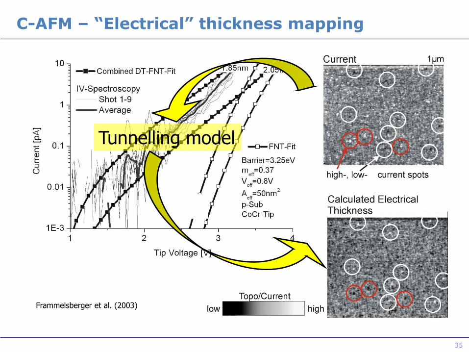
C-AFM – “Electrical” thickness mapping
Frammelsberger et al. (2003)
C-AFM – Combined methods
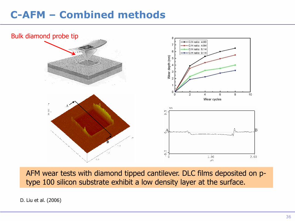
36
AFM wear tests with diamond tipped cantilever. DLC films deposited on p-type 100 silicon substrate exhibit a low density layer at the surface.
Bulk diamond probe tip
D. Liu et al. (2006)
C-AFM – Combined methods
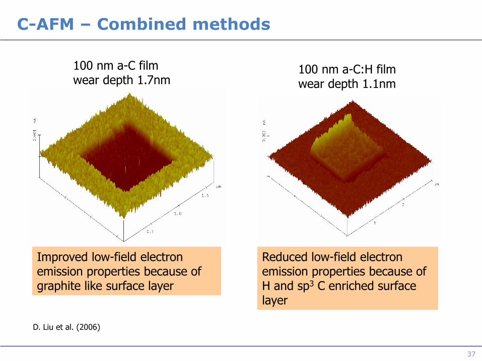
37
Reduced low-field electron emission properties because of H and sp3 C enriched surface layer
100 nm a-C film wear depth 1.7nm
100 nm a-C:H film wear depth 1.1nm
Improved low-field electron emission properties because of graphite like surface layer
D. Liu et al. (2006)
C-AFM – Combined methods
38
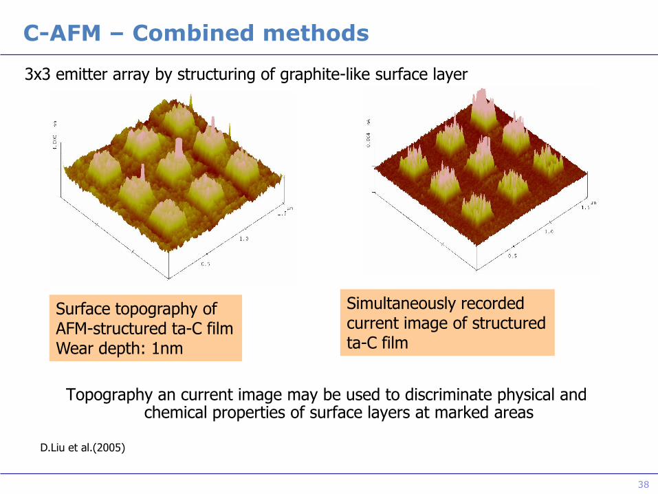
Surface topography of AFM-structured ta-C film Wear depth: 1nm
Simultaneously recorded current image of structured ta-C film
3x3 emitter array by structuring of graphite-like surface layer
D.Liu et al.(2005)
Topography an current image may be used to discriminate physical and chemical properties of surface layers at marked areas
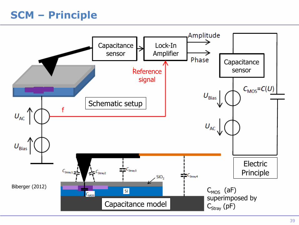
SCM – Principle
39
Biberger (2012)
Schematic setup
Capacitance sensor
Lock-In Amplifier
Electric Principle
Capacitance sensor Reference
signal
Capacitance model
CMOS (aF) superimposed by CStray (pF)
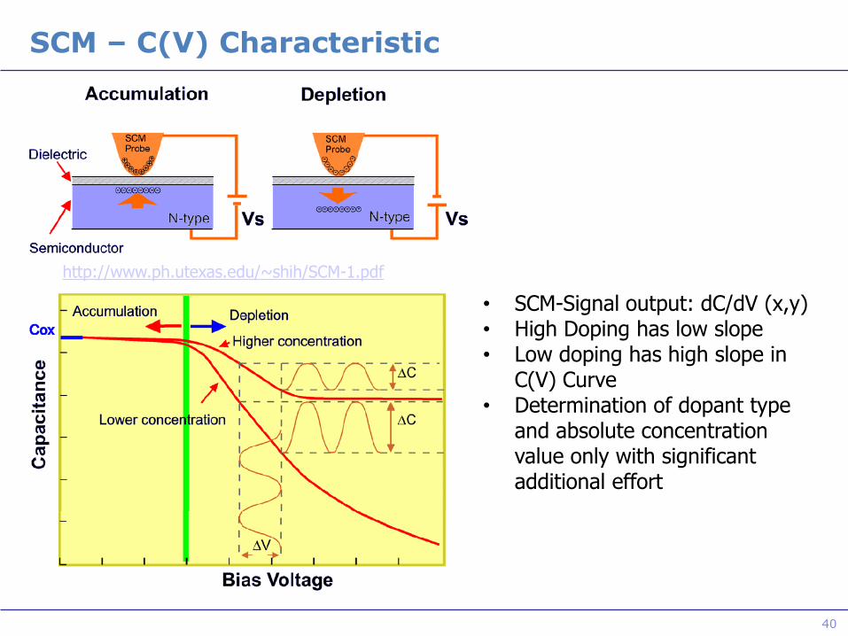
SCM – C(V) Characteristic
40
• SCM-Signal output: dC/dV (x,y) • High Doping has low slope • Low doping has high slope in
C(V) Curve • Determination of dopant type
and absolute concentration value only with significant additional effort
http://www.ph.utexas.edu/~shih/SCM-1.pdf
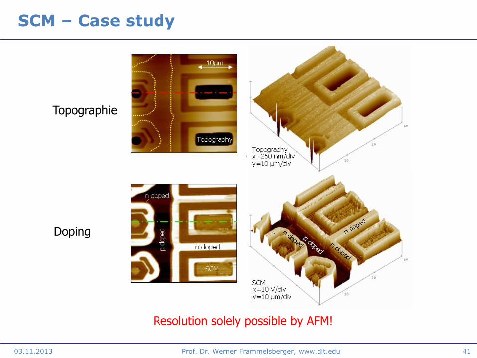
SCM – Case study
03.11.2013 41
Topographie
Doping
Resolution solely possible by AFM!
Prof. Dr. Werner Frammelsberger, www.dit.edu
42
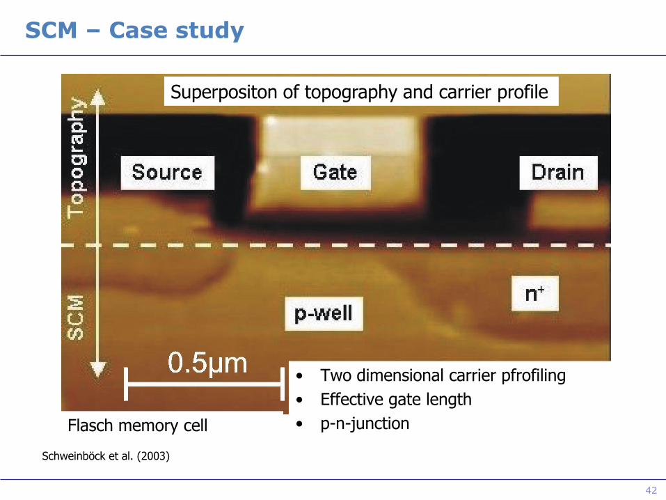
SCM – Case study
Superpositon of topography and carrier profile
Flasch memory cell
• Two dimensional carrier pfrofiling
• Effective gate length
• p-n-junction
Schweinböck et al. (2003)
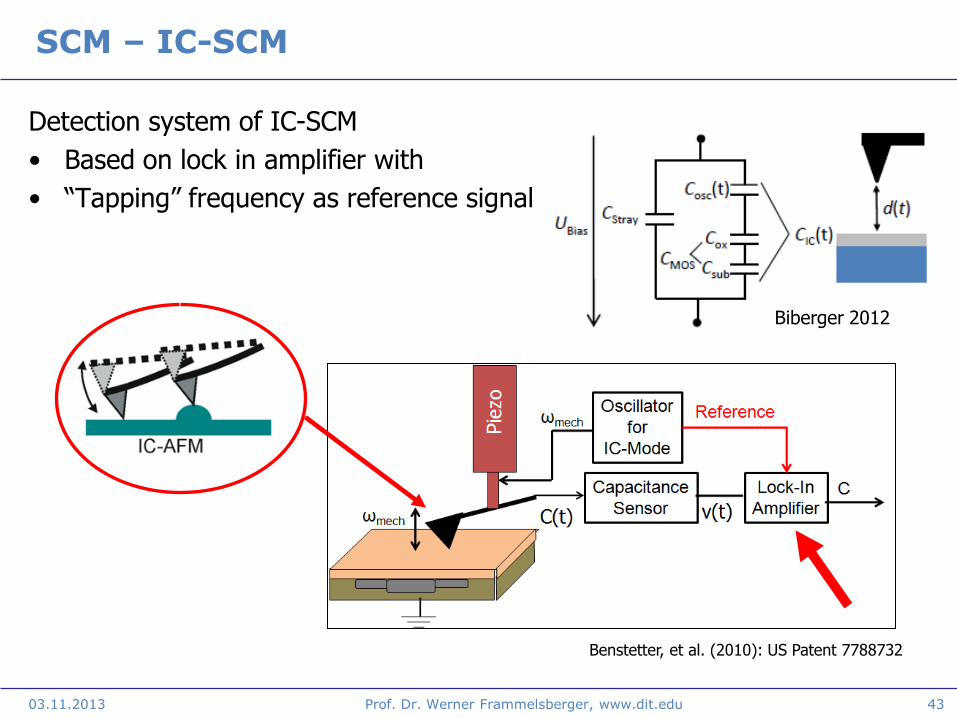
SCM – IC-SCM
Detection system of IC-SCM
• Based on lock in amplifier with
• “Tapping” frequency as reference signal
03.11.2013 Prof. Dr. Werner Frammelsberger, www.dit.edu 43
Benstetter, et al. (2010): US Patent 7788732
Biberger 2012
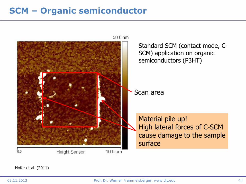
SCM – Organic semiconductor
44
Standard SCM (contact mode, C-SCM) application on organic semiconductors (P3HT)
Material pile up! High lateral forces of C-SCM cause damage to the sample surface
Scan area
Hofer et al. (2011)
03.11.2013 Prof. Dr. Werner Frammelsberger, www.dit.edu
IC-SCM – Organic Semiconductor
45
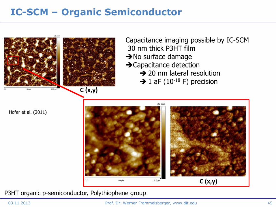
Capacitance imaging possible by IC-SCM 30 nm thick P3HT film No surface damage Capacitance detection
20 nm lateral resolution 1 aF (10-18 F) precision
C (x,y)
C (x,y)
P3HT organic p-semiconductor, Polythiophene group
Hofer et al. (2011)
03.11.2013 Prof. Dr. Werner Frammelsberger, www.dit.edu
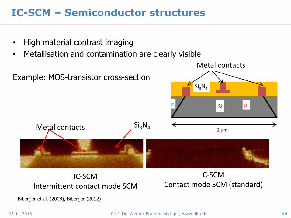
IC-SCM – Semiconductor structures
03.11.2013 46
C-SCM Contact mode SCM (standard)
IC-SCM Intermittent contact mode SCM
Metal contacts Si3N4
Metal contacts
• High material contrast imaging
• Metallisation and contamination are clearly visible
Example: MOS-transistor cross-section
Biberger et al. (2008), Biberger (2012)
Prof. Dr. Werner Frammelsberger, www.dit.edu
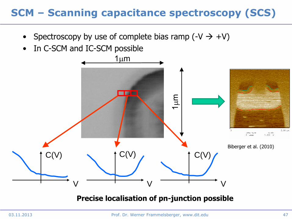
SCM – Scanning capacitance spectroscopy (SCS)
• Spectroscopy by use of complete bias ramp (-V +V)
• In C-SCM and IC-SCM possible
47
Precise localisation of pn-junction possible
C(V)
V
C(V) C(V)
V V
Biberger et al. (2010)
03.11.2013 Prof. Dr. Werner Frammelsberger, www.dit.edu
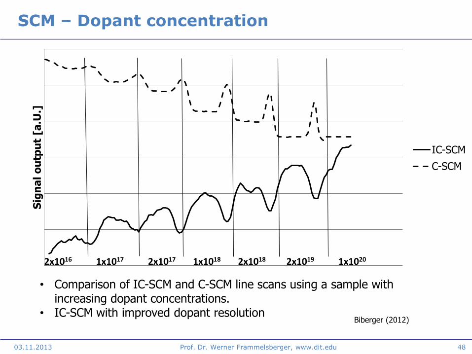
SCM – Dopant concentration
03.11.2013 Prof. Dr. Werner Frammelsberger, www.dit.edu 48
Sig
na
l o
utp
ut
[a.U
.]
IC-SCM
C-SCM
1x10¹⁸
2x10¹⁸ 2x10¹⁹ 1x10²⁰ 2x10¹⁶ 1x10¹⁷ 2x10¹⁷
• Comparison of IC-SCM and C-SCM line scans using a sample with increasing dopant concentrations.
• IC-SCM with improved dopant resolution Biberger (2012)
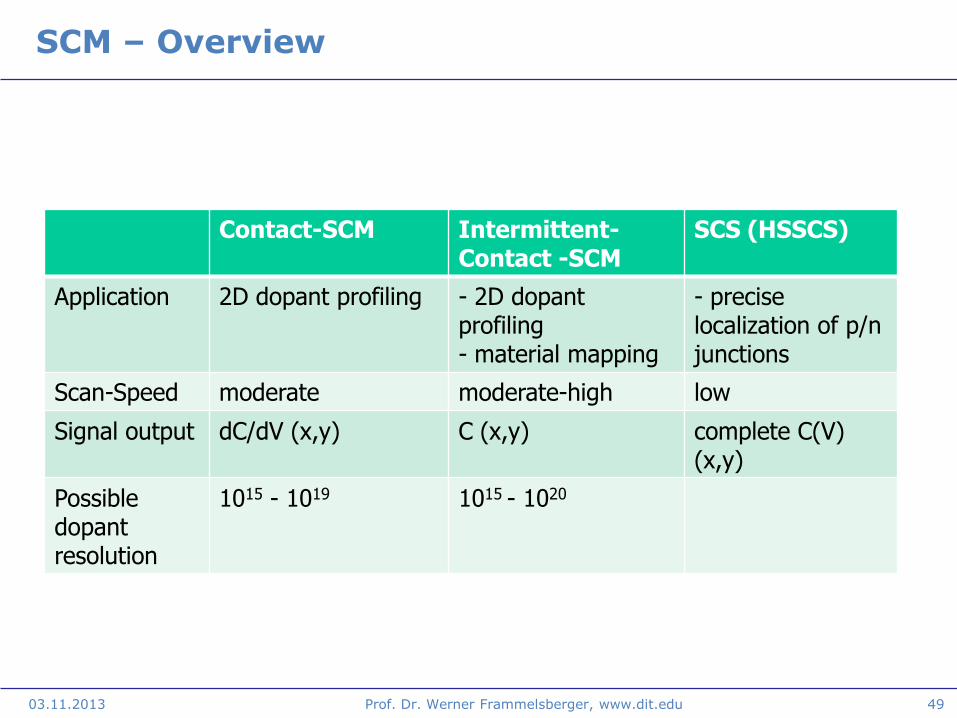
SCM – Overview
03.11.2013 Prof. Dr. Werner Frammelsberger, www.dit.edu 49
Contact-SCM Intermittent-Contact -SCM
SCS (HSSCS)
Application 2D dopant profiling - 2D dopant profiling - material mapping
- precise localization of p/n junctions
Scan-Speed moderate moderate-high low
Signal output dC/dV (x,y) C (x,y) complete C(V) (x,y)
Possible dopant resolution
1015 - 1019 1015 - 1020
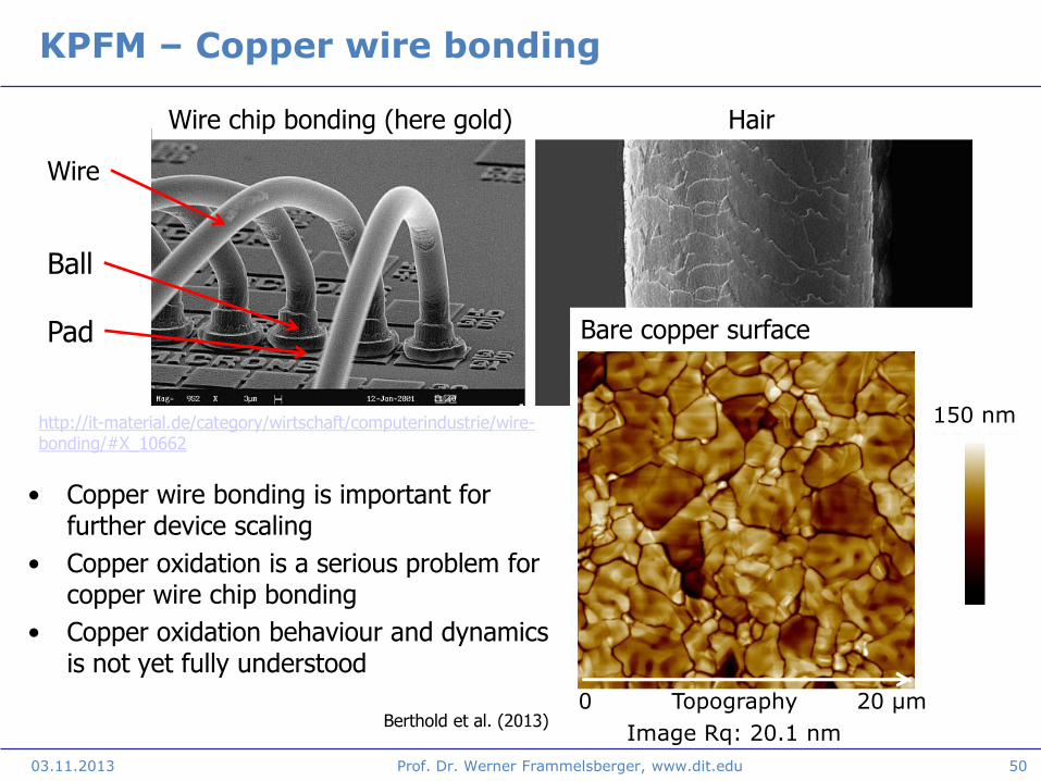
KPFM – Copper wire bonding
03.11.2013 Prof. Dr. Werner Frammelsberger, www.dit.edu 50
Berthold et al. (2013)
http://it-material.de/category/wirtschaft/computerindustrie/wire-bonding/#X_10662
• Copper wire bonding is important for further device scaling
• Copper oxidation is a serious problem for copper wire chip bonding
• Copper oxidation behaviour and dynamics is not yet fully understood
Topography0 20 µm
150 nm
Image Rq: 20.1 nm
Bare copper surface
Wire
Ball
Pad
Wire chip bonding (here gold) Hair
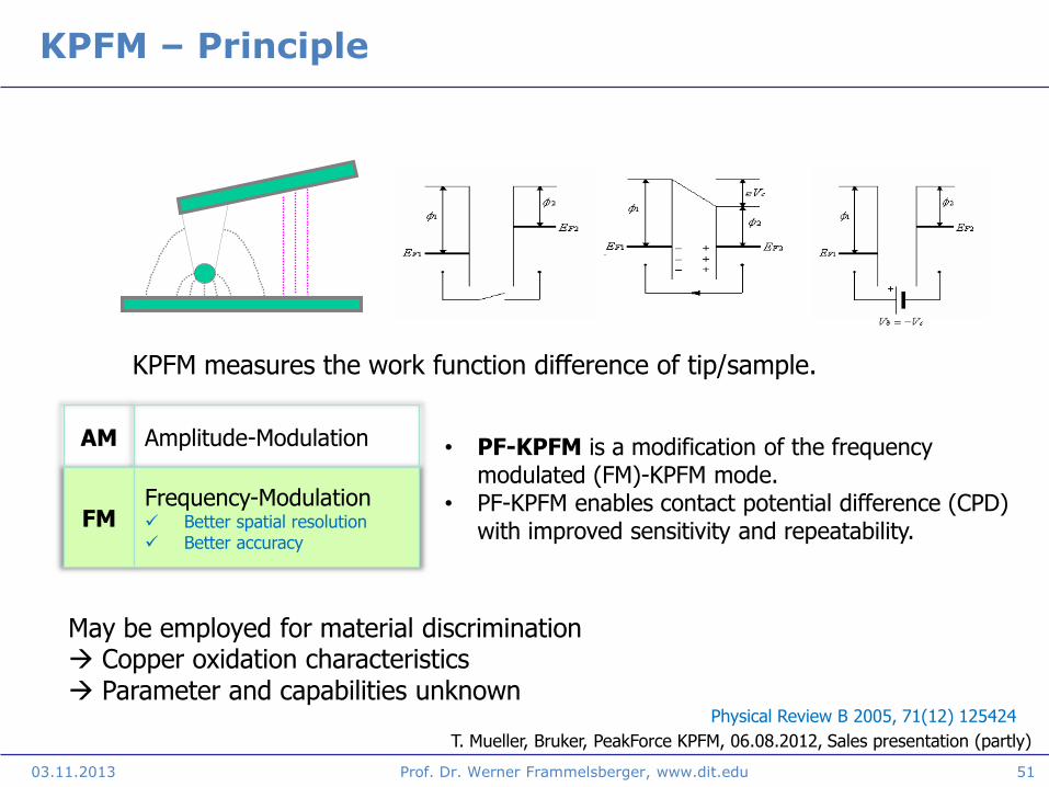
KPFM – Principle
03.11.2013 Prof. Dr. Werner Frammelsberger, www.dit.edu 51
AM Amplitude-Modulation
FM Frequency-Modulation Better spatial resolution Better accuracy
Physical Review B 2005, 71(12) 125424
KPFM measures the work function difference of tip/sample.
T. Mueller, Bruker, PeakForce KPFM, 06.08.2012, Sales presentation (partly)
May be employed for material discrimination Copper oxidation characteristics Parameter and capabilities unknown
• PF-KPFM is a modification of the frequency modulated (FM)-KPFM mode.
• PF-KPFM enables contact potential difference (CPD) with improved sensitivity and repeatability.
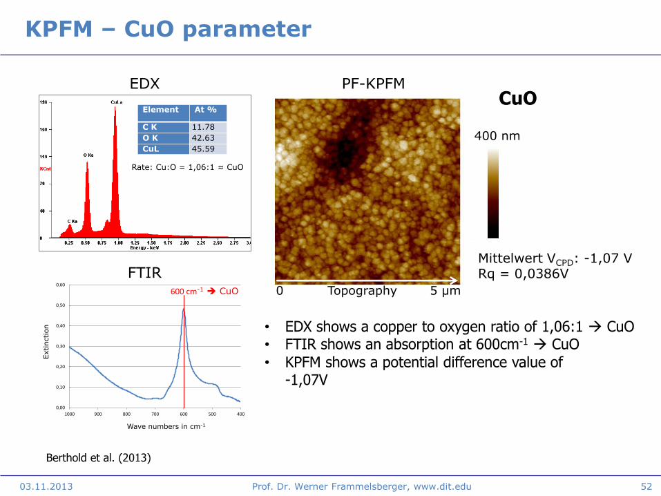
KPFM – CuO parameter
52
Topography0 5 µm
400 nm
Element At %
C K 11.78
O K 42.63
CuL 45.59
Rate: Cu:O = 1,06:1 ≈ CuO
Mittelwert VCPD: -1,07 V Rq = 0,0386V
EDX PF-KPFM
• EDX shows a copper to oxygen ratio of 1,06:1 CuO • FTIR shows an absorption at 600cm-1 CuO
• KPFM shows a potential difference value of -1,07V
CuO
Wave numbers in cm-1
Extinction
0,00
0,10
0,20
0,30
0,40
0,50
0,60
4005006007008009001000
600 cm-1 CuO
FTIR
Berthold et al. (2013)
03.11.2013 Prof. Dr. Werner Frammelsberger, www.dit.edu
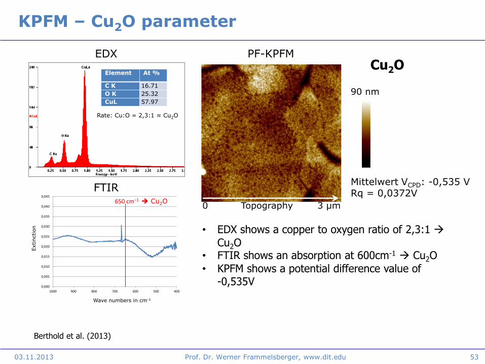
KPFM – Cu2O parameter
03.11.2013 Prof. Dr. Werner Frammelsberger, www.dit.edu 53
Element At %
C K 16.71
O K 25.32
CuL 57.97
Rate: Cu:O = 2,3:1 ≈ Cu2O
0,000
0,005
0,010
0,015
0,020
0,025
0,030
0,035
0,040
0,045
4005006007008009001000
Wave numbers in cm-1
Extinction
650 cm-1 Cu2O Topography0 3 µm
90 nm
Mittelwert VCPD: -0,535 V Rq = 0,0372V
EDX
FTIR
PF-KPFM
• EDX shows a copper to oxygen ratio of 2,3:1
Cu2O • FTIR shows an absorption at 600cm-1 Cu2O
• KPFM shows a potential difference value of -0,535V
Cu2O
Berthold et al. (2013)
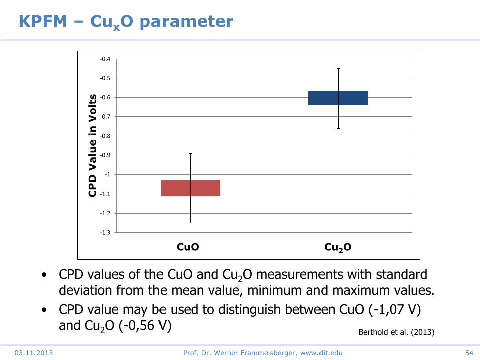
KPFM – CuxO parameter
• CPD values of the CuO and Cu2O measurements with standard deviation from the mean value, minimum and maximum values.
• CPD value may be used to distinguish between CuO (-1,07 V) and Cu2O (-0,56 V)
03.11.2013 Prof. Dr. Werner Frammelsberger, www.dit.edu 54
-1.3
-1.2
-1.1
-1
-0.9
-0.8
-0.7
-0.6
-0.5
-0.4
CP
D V
alu
e i
n V
olt
s
CuO Cu2O
Berthold et al. (2013)
55
Summary
• AFM based techniques enable high resolution structural and physical
characterisation of materials and thin films
• Probe tip and AFM operation mode is critical to quality and reliability of
results
• AFM-techniques operating in contact mode are critical with respect to
sample interference and tip wear
• It is possible to transfer originally contact mode applications to
intermittent contact mode applications and
– to extend the measurement capabilities
– to increase quality and reliability of the results
• Combination of different AFM methods as well as combination of AFM
methods and SEM based techniques may further extent analysis
capabilities
• As martial properties in the nanometre scale become increasingly
important, research is necessary to keep pace with applicable and
reliable analysis methods
03.11.2013 Prof. Dr. Werner Frammelsberger, www.dit.edu
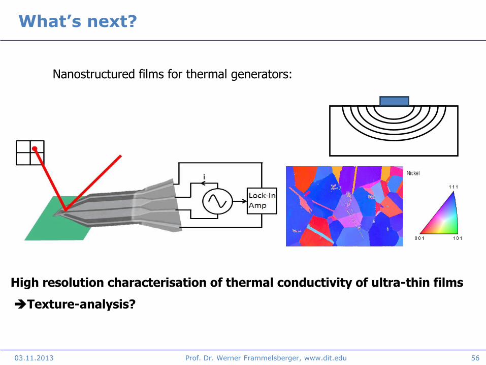
What’s next?
56
High resolution characterisation of thermal conductivity of ultra-thin films
Texture-analysis?
Nanostructured films for thermal generators:
03.11.2013 Prof. Dr. Werner Frammelsberger, www.dit.edu
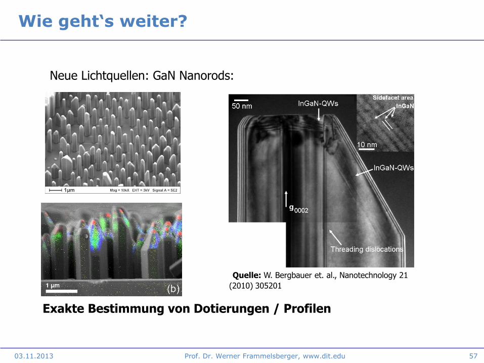
Wie geht‘s weiter?
03.11.2013 57
Exakte Bestimmung von Dotierungen / Profilen
Neue Lichtquellen: GaN Nanorods:
Quelle: W. Bergbauer et. al., Nanotechnology 21
(2010) 305201
Prof. Dr. Werner Frammelsberger, www.dit.edu
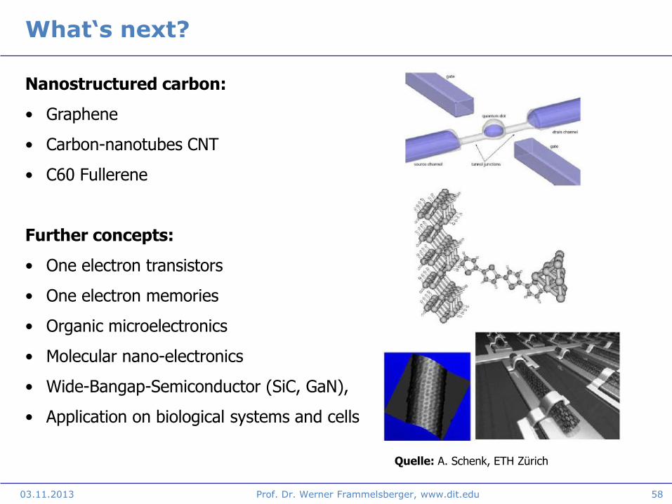
What‘s next?
03.11.2013 58
Nanostructured carbon:
• Graphene
• Carbon-nanotubes CNT
• C60 Fullerene
Further concepts:
• One electron transistors
• One electron memories
• Organic microelectronics
• Molecular nano-electronics
• Wide-Bangap-Semiconductor (SiC, GaN),
• Application on biological systems and cells
Quelle: A. Schenk, ETH Zürich
Prof. Dr. Werner Frammelsberger, www.dit.edu
Further reading
03.11.2013 Prof. Dr. Werner Frammelsberger, www.dit.edu 59
• Benstetter, G.; Breitschopf, P.; Frammelsberger, W.; Ranzinger, H.; Reislhuber, P.; Schweinboeck, T. (2004): AFM-based scanning capacitance techniques for deep sub-micron semiconductor failure analysis. ESREF, European Symposium on the Reliability of Electron Devices, Failure Physics and Analysis, 15. In: Microelectronics Reliability 44 (9-11), S. 1615–1619.
• Benstetter, Guenther; Breitschopf, Peter; Knoll, Bernhard (2010): Method and apparatus for two-dimensional profiling of doping profiles of a material sample with scanning capacitance microscope. Anmeldenr: US 11/726,590. Veröffentlichungsnr: US7788732 B2.
• Benstetter, Günther; Biberger, Roland; Liu, Dongping (2009): A review of advanced scanning probe microscope analysis of functional films and semiconductor devices. 4th International Conference on Technological Advances of Thin Films and Surface Coatings. In: Thin Solid Films 517 (17), S. 5100–5105.
• Bergbauer, W.; Strassburg, M.; Kölper, Ch; Linder, N.; Roder, C.; Lähnemann, J. et al. (2010): Continuous-flux MOVPE growth of position-controlled N-face GaN nanorods and embedded InGaN quantum wells. In: Nanotechnology 21 (30), S. 305201.
• Biberger, Roland; Benstetter, Guenther; Goebel, Holger; Hofer, Alexander (2010): Intermittent-contact capacitance spectroscopy – A new method for determining C(V) curves with sub-micron lateral resolution. 21st European Symposium on the Reliability of Electron Devices, Failure Physics and Analysis. In: Microelectronics Reliability 50 (9–11), S. 1511–1513.
• Biberger, Roland; Benstetter, Guenther; Schweinboeck, Thomas; Breitschopf, Peter; Goebel, Holger (2008): Intermittent-contact scanning capacitance microscopy versus contact mode SCM applied to 2D dopant profiling. 19th European Symposium on Reliability of Electron Devices, Failure Physics and Analysis (ESREF 2008). In: Microelectronics Reliability 48 (8–9), S. 1339–1342.
Further reading
03.11.2013 Prof. Dr. Werner Frammelsberger, www.dit.edu 60
• Frammelsberger, W.; Benstetter, G.; Schweinboeck, T.; Stamp, R.; Kiely, J. (2003): Advanced Analysis of Thin and Ultrathin SiO~2 Films and SiO~2/Si Interfaces with Combined Atomic Force Microscopy Methods. In: Proceedings of the 29th International Symposium for Testing and Failure Analysis. 2 - 6 November 2003, Santa Clara Convention Center, Santa Clara, California. ISTFA 2003; International Symposium for Testing and Failure Analysis. Materials Park, Ohio: ASM International, S. 406–4012.
• Frammelsberger, Werner (2006): Improved atomic force microscopy based techniques for electrical and structural characterisation of thin dielectric films. University of the West of England, Bristol.
• Frammelsberger, Werner; Benstetter, Guenther; Kiely, Janice; Stamp, Richard (2006): Thickness determination of thin and ultra-thin SiO2 films by C-AFM IV-spectroscopy. In: Applied Surface Science 252 (6), S. 2375–2388.
• Frammelsberger, Werner; Benstetter, Guenther; Kiely, Janice; Stamp, Richard (2007): C-AFM-based thickness determination of thin and ultra-thin SiO2 films by use of different conductive-coated probe tips. In: Applied Surface Science 253 (7), S. 3615–3626.
• Frammelsberger, Werner; Benstetter, Guenther; Schweinboeck, Thomas; Stamp, Richard J.; Kiely, Janice (2003): Characterization of thin and ultra-thin SiO2 films and SiO2/Si interfaces with combined conducting and topographic atomic force microscopy. 14th European Symposium on Reliability of Electron Devices, Failure Physics and Analysis. In: Microelectronics Reliability 43 (9–11), S. 1465–1470.
Further reading
03.11.2013 Prof. Dr. Werner Frammelsberger, www.dit.edu 61
• Frammelsberger, Werner; Benstetter, Guenther; Stamp, Richard; Kiely, Janice; Schweinboeck, Thomas (2005): Simplified tunnelling current calculation for MOS structures with ultra-thin oxides for conductive atomic force microscopy investigations. In: Materials Science and Engineering: B 116 (2), S. 168–174.
• Hofer, Alexander; Benstetter, Günther; Biberger, Roland; Leirer, Christian; Brüderl, Georg (2013): Analysis of crystal defects on GaN-based semiconductors with advanced scanning probe microscope techniques. In: Thin Solid Films.
• Hofer, Alexander; Biberger, Roland; Wilke, Bjoern; Benstetter, Guenther; Goebel, Holger (2011): Capacitance and Conductivity Mapping of Organic Films and Devices with Non-Contact SPM Methods.
• Liu, Dongping; Benstetter, Guenther; Frammelsberger, Werner (2006): Nanoscale electron field emissions from the bare, hydrogenated, and graphitelike-layer-covered tetrahedral amorphous carbon films. In: Journal of Applied Physics 99 (4), S. 44303.
• Liu, Dongping; Benstetter, Günther (2005): Conducting atomic force microscopy for nanoscale electron emissions from various diamond-like carbon films. In: Applied Surface Science 249 (1–4), S. 315–321.
• Schweinbock, T.; Schomann, S.; Alvarez, D.; Buzzo, M.; Frammelsberger, W.; Breitschopf, P.; Benstetter, G. (2004): New trends in the application of scanning probe techniques in failure analysis. ESREF, European Symposium on the Reliability of Electron Devices, Failure Physics and Analysis, 15. In: Microelectronics Reliability 44 (9-11), S. 1541–1546.
Partner
03.11.2013 62
• Kooperative Promotionen
• Verbesserung von organischen
Halbleiter-Strukturen
• Kooperative Promotionen
• Untersuchung von Silizium
Halbleiter Ausfallmechanismen
• Untersuchung von nanorod
LED-Strukturen
• Org. „Thin –Films“-Konferenz
• Dünnschicht-Charakterisierung
• Gem. Forschungskolleg
beantragt
• Kooperation RSM
• Charakterisierung von DLC Schichten • Opt. von Plasmaprozessen
• Dünnschicht-Charakterisierung • Opt. von Plasmaprozessen
Prof. Dr. Werner Frammelsberger, www.dit.edu
Partner
03.11.2013 Fakultät Maschinenbau und Mechatronik, Prof. Dr. Werner Frammelsberger 63
• Kooperative Promotionen • Biologische AFM-Anwendung
• Untersuchung der Ausfallmechanismen von LED/Laser Strukturen
• Oberflächen-Charakterisierung • Opt. von Plasmaprozessen
Die Projekte werden ganz oder Teilweise gefördert durch verschiedene Förderprojekte des
• Freistaates Bayern
• Bundesministeriums für Bildung und Forschung
Partner
03.11.2013 Fakultät Maschinenbau und Mechatronik, Prof. Dr. Werner Frammelsberger 64
• AFM-Analytik
• Prozesskontrolle • Silizium-Wafertests
• Untersuchung von nanorod LED-
Strukturen
• Untersuchung von
Kupferbonds
• Vergleichsmessungen
• Verbesserung der LockIn-
Verstärkertechnik
• Vergleichsmessungen
• Untersuchung der Ausfallmechanismen von LED/Laser Strukturen
• Umsetzung eines Messplatzes für chemical RSM
• Verwertung der Ergebnisse • Vermarktung
03.11.2013 Fakultät Maschinenbau und Mechatronik, Prof. Dr. Werner Frammelsberger 65


