
1 05/02/2018
MOC306x
DD93230
DESCRIPTION
The MOC306x Series are optically coupled isolators consisting of a Gallium Arsenide infrared emitting diode coupled with a monolithic silicon detector performing the functions of a zero crossing bilateral triac mounted in a standard 6 pin dual-in-line package. FEATURES
• Zero Voltage Crossing • Triac Driver Output • High VDRM minimum 600V • High Critical Rate of Rise of Off-State Voltage
dv/dt minimum 600V/μs • Isolation Voltage 5000VRMS • RoHS Compliant • UL File No. E91231 Package System “TT” • VDE File No. 40028086 APPLICATIONS
• Solenoid / Valve Controls • Light Controls • AC Motor Drivers • Temperature Controls • AC Motor Starters • Solid State Relays ORDER INFORMATION
• Add Suffix “X” for VDE Approval • Add G after PN for 10mm lead spacing • Add SM after PN for Surface Mount • Add SMT&R after PN for Surface Mount
Tape & Reel
ABSOLUTE MAXIMUM RATINGS TA = 25°C unless otherwise specified. Stresses exceeding the absolute maximum ratings can cause permanent damage to the device. Exposure to absolute maximum ratings for long periods of time can adversely affect reliability.
ISOCOM COMPONENTS 2004 LTD Unit 25B, Park View Road West, Park View Industrial Estate
Hartlepool, Cleveland, TS25 1PE, United Kingdom Tel: +44 (0)1429 863 609 Fax : +44 (0)1429 863 581
e-mail: [email protected] http://www.isocom.com
ISOCOM COMPONENTS ASIA LTD Hong Kong Office,
Block A, 8/F, Wah Hing Industrial mansion, 36 Tai Yau Street, San Po Kong, Kowloon, Hong Kong.
Tel: +852 2995 9217 Fax : +852 8161 6292 e-mail [email protected]
Forward Current 50mA Reverse Voltage 6V
Power dissipation 120mW
Input
Juntion Temperature 125°C
Peak Repetitive Surge Current (Pulse Width 100μs, 120pps)
1.0A
Junction Temperature 125°C
Power Dissipation 150mW
Output
On State RMS Current 100mARMS
Off State Output Terminal Voltage 600V
Isolation Voltage 5000VRMS Total Power Dissipation 250mW Operating Temperature -40 to 100°C
Storage Temperature -55 to 150°C Lead Soldering Temperature (10s) 260°C
Total Package
1 Anode
2 Cathode
3 NC
4 Main Terminal 1
5 Substrate, (Do not Connect)
6 Main Terminal 2

2 05/02/2018
MOC306x
DD93230
ELECTRICAL CHARACTERISTICS (TA = 25°C unless otherwise specified)
Parameter Symbol Test Condition Min Typ. Max Unit
Forward Voltage VF IF = 20mA 1.2 1.4 V
Reverse Current IR VR = 6V 0.05 10 μA
INPUT
Parameter Symbol Test Condition Min Typ. Max Unit
Peak Off-state Current Either Direction
IDRM VDRM = 600V IF = 0mA
Note 1
500 nA
Peak Blocking Voltage Either Direction
VDRM IDRM = 500nA 600 V
On-state Voltage Either Direction
VTM ITM = 100mA (peak)
3.0 V
Critical Rate of Rise of Off-state Voltage (Static dv/dt)
dv/dt IF = 0mA, Vin = 240VRMS
1000 V/μs
OUTPUT
Parameter Symbol Test Condition Min Typ. Max Unit
Input Trigger Current Either Direction
IFT VTM = 3V
Note 2
mA
MOC3060 30
MOC3061 15
MOC3062 10
MOC3063 5
Holding Current Either Direction
IH 400 μA
COUPLED

3 05/02/2018
MOC306x
DD93230
ELECTRICAL CHARACTERISTICS (TA = 25°C unless otherwise specified) Note 1 : Test Voltage must be applied within dv/dt rating. Note 2 : Guaranteed to trigger at an IF value less than or equal to max IFT, recommended IF lies between Rated IFT to Absolute Max IF. Note 3 : Measured with input leads shorted together and output leads shorted together.
Parameter Symbol Test Condition Min Typ. Max Unit
Inhibit Voltage VINH IF = Rated IFT, MT1-MT2 Voltage above which
device will not trigger
5
20 V
Leakage Current at Inhibit State
IDRM2 IF = Rated IFT, VDRM = 600V,
Off-state
500 μA
ZERO CROSSING CHARACTERISTICS
Parameter Symbol Test Condition Min Typ. Max Unit
Isolation Voltage Input-Output
VISO RH = 40 to 60%, t = 1 min
Note 3
5000 VRMS
ISOLATION

4 05/02/2018
MOC306x
DD93230
Fig 1 Forward Current vs Ambient Temperature Fig 2 On-State Current vs Ambient Temperature
Fig 3 Forward Current vs Forward Voltage Fig 4 On-state Current vs On-State Voltage
Fig 5 Minimum Trigger Current vs Ambient Temperature
Fig 6 On-State Voltage vs Ambient Temperature
5 05/02/2018
MOC306x
DD93230
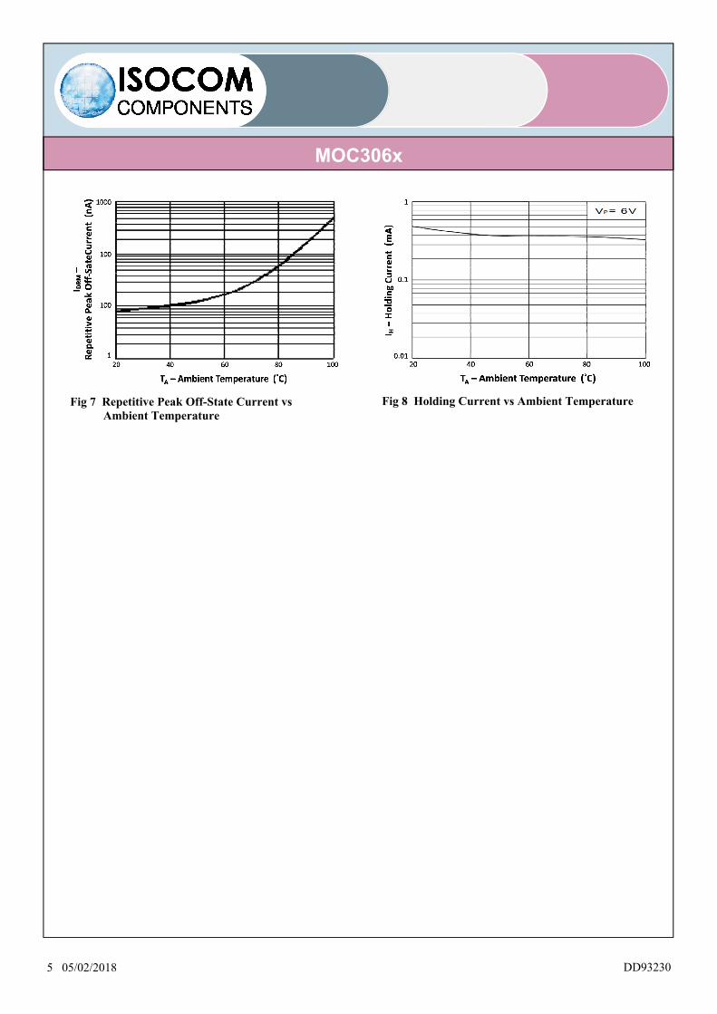
Fig 7 Repetitive Peak Off-State Current vs Ambient Temperature
Fig 8 Holding Current vs Ambient Temperature

6 05/02/2018
MOC306x
DD93230
After PN Description Packing quantity
None Standard DIP6 65 pcs per tube
G 10mm Lead Spacing 65 pcs per tube
SM Surface Mount 65 pcs per tube
SMT&R Surface Mount Tape & Reel 1000 pcs per reel
MOC306x (UL Approval)
PN
MOC3060, MOC3061, MOC3062, MOC3063
MOC3060G, MOC3061G, MOC3062G, MOC3063G
MOC3060SM, MOC3061SM, MOC3062SM, MOC3063SM
MOC3060SMT&R, MOC3061SMT&R, MOC3062SMT&R, MOC3063SMT&R
ORDER INFORMATION
After PN Description Packing quantity
None Standard DIP6 65 pcs per tube
G 10mm Lead Spacing 65 pcs per tube
SM Surface Mount 65 pcs per tube
SMT&R Surface Mount Tape & Reel 1000 pcs per reel
MOC306x (UL and VDE Approvals)
PN
MOC3060X, MOC3061X, MOC3062X, MOC3063X
MOC3060XG, MOC3061XG, MOC3062XG, MOC3063XG
MOC3060XSM, MOC3061XSM, MOC3062XSM, MOC3063XSM
MOC3060XSMT&R, MOC3061XSMT&R, MOC3062XSMT&R, MOC3063XSMT&R

7 05/02/2018
MOC306x
DD93230
DEVICE MARKING Example : MOC3063X
MOC3063X Denotes Device Part Number I denotes Isocom
Y denotes 2 digit Year code WW denotes 2 digit Week code
TT UL Package System Code
MOC3063X
I YWW TT

8 05/02/2018
MOC306x
DD93230
DIP
G Form
SMD
PACKAGE DIMENSIONS in mm (inch)

9 05/02/2018
MOC306x
DD93230
TAPE AND REEL PACKAGING RECOMMENDED PAD LAYOUT for SMD (mm)
Description Symbol Dimension mm (inch)
Tape Width W 16 ± 0.3 (0.63)
Pitch of Sprocket Holes P0 4 ± 0.1 (0.15)
F 7.5 ± 0.1 (0.295)
P2 2 ± 0.1 (0.079)
Distance of Compartment to Compartment P1 12 ± 0.1 (0.47)
Distance of Compartment to Sprocket Holes

10 05/02/2018
MOC306x
DD93230
IR REFLOW SOLDERING TEMPERATURE PROFILE One Time Reflow Soldering is Recommended. Do not immerse device body in solder paste.
TIME (s)
TEM
P (°
C)
25°C
ts Preheat 60s – 120s
Tsmin
Tsmax
260°C
TL 217°C
Time 25°C to Peak Temperature
tP
TP - 5°C TP
Max Ramp Up Rate 3°C/s
Max Ramp Down Rate 6°C/s
TL 200°C
150°C
Profile Details Conditions
Preheat - Min Temperature (TSMIN) - Max Temperature (TSMAX) - Time TSMIN to TSMAX (ts)
150°C 200°C 60s - 120s
Soldering Zone - Peak Temperature (TP) - Time at Peak Temperature - Liquidous Temperature (TL) - Time within 5°C of Actual Peak Temperature (TP ̶ 5°C) - Time maintained above TL (tL) - Ramp Up Rate (TL to TP) - Ramp Down Rate (TP to TL)
260°C 10s max 217°C 30s max 60s - 100s 3°C/s max 6°C/s max
Average Ramp Up Rate (Tsmax to TP) 3°C/s max
Time 25°C to Peak Temperature 8 minutes max

11 05/02/2018
DISCLAIMER
DD93230
Isocom Components is continually working to improve the quality and reliability of its products. Nevertheless, semiconductor devices in general can malfunction or fail due to their inherent electrical sensitivity and vulnerability to physical stress. It is the responsibility of the buyer, when utilizing Isocom Components products, to comply with the standards of safety in making a safe design for the entire system, and to avoid situations in which a malfunction or failure of such Isocom Components products could cause loss of human life, bodily injury or damage to property. In developing your designs, please ensure that Isocom Components products are used within specified operating ranges as set forth in the most recent Isocom Components products specifications. The Isocom Components products listed in this document are intended for usage in general electronics applications (computer, personal equipment, office equipment, measuring equipment, industrial robotics, domestic appliances, etc.). These Isocom Components products are neither intended nor warranted for usage in equipment that requires extraordinarily high quality and/or reliability or a malfunction or failure of which may cause loss of human life or bodily injury (“Unintended Usage”). Unintended Usage include atomic energy control instruments, airplane or spaceship instruments, transportation Instruments, traffic signal instruments, combustion control instruments, medical Instruments, all types of safety devices, etc... Unintended Usage of Isocom Components products listed in this document shall be made at the customer’s own risk. Gallium arsenide (GaAs) is a substance used in the products described in this document. GaAs dust and fumes are toxic. Do not break, cut or pulverize the product, or use chemicals to dissolve them. When disposing of the products, follow the appropriate regulations. Do not dispose of the products with other industrial waste or with domestic garbage. The products described in this document are subject to the foreign exchange and foreign trade laws. The information contained herein is presented only as a guide for the applications of our products. No responsibility is assumed by Isocom Components for any infringements of intellectual property or other rights of the third parties which may result from its use. No license is granted by implication or otherwise under any intellectual property or other rights of Isocom Components or others. The information contained herein is subject to change without notice.


