Download - Mos Slides
1
Chapter 1: MOSFET operation

2
Outline
• Introduction • Long-channel transistor • Small-geometry effects • Small-signal behavior at low frequencies • Capacitors and parasitic resistors • Evaluation of MOS performance in Matlab

3
Outline
• Introduction • Long-channel transistor • Small-geometry effects • Small-signal behavior at low frequencies • Capacitors and parasitic resistors • Evaluation of MOS performance in Matlab

4
Microelectronics obeys Moore’s law = Exponential growth of # transistors on a chip Roadmap according to this law: International
Technology Roadmap for Semiconductors (ITRS), see http://public.itrs.net
[www.intel.com]

5
ITRS predicts CMOS downscaling until 2020
• Upgrade of technology yields reduction in area per function and energy consumption per logical operation
• CMOS speed increases → CMOS is also used nowadays for radio-frequency (RF) applications
1st year of production
Technology generation
2004 90 nm
2007 65 nm
2009 45 nm
2011 32 nm
2013 22 nm
2015 14 nm
200
400
600
800
1000
1200
1400
20406080100C
utof
f fre
quen
cy f T [G
Hz]
Gate length [nm]
ITRS 2003
fT
fT is a measure for the transistor speed (see later)

6
CMOS has replaced bipolar and GaAs in various wireless products antenna
digi
tal
Commercial CMOS radio ICs for GSM, DECT, Bluetooth, GPS, WLAN, …
CMOS prototype for 60GHz wireless communication (UC Berkeley, 2007)

7
Ideal MOS transistor in saturation is … a (voltage-)controlled current source
|VOVER| (V)
|iTHROUGH| (A)
|VCONTROL|=|VCONTROL1| |VCONTROL|=|VCONTROL2| (> |VCONTROL1|) |VCONTROL|=|VCONTROL3| (> |VCONTROL2|)
|VCONTROL|=|VCONTROL4| (> |VCONTROL3|) |VCONTROL|=|VCONTROL5| (> |VCONTROL4|)
|VCONTROL|=|VCONTROL6| (> |VCONTROL5|)
|VCONTROL|=|VCONTROL7| (> |VCONTROL6|)
saturation
incr
easi
ng |V
GS|
ITHROUGH vOVER
vCONTROL
vCONTROL
ITHROUGH vOVER
iTHROUGH vCONTROL
+
-

8
Symbols for an n-MOS transistor
Gate
Drain
Source
More complete:
Gate
Drain
Source
Bulk normal current flow IDS
normal operation: VGS > 0 VDS ≥ 0 VSB ≥ 0
VDS (V)
iDS (A)
VGS=VGS1
VGS=VGS2 (> VGS1) VGS=VGS3 (> VGS2)
VGS=VGS4 (> VGS3) VGS=VGS5 (> VGS4)
VGS=VGS6 (> VGS5)
VGS=VGS7 (> VGS6)
saturation
Mor
e po
sitiv
e V
GS

9
Symbols for a p-MOS transistor
normal operation: VGS < 0 VDS ≤ 0 VSB ≤ 0
Gate
Drain
Source
normal current flow IDS
More complete:
Gate
Source
Bulk
Drain
|VDS| (V)
|iDS| (A)
|VGS|=|VGS1| |VGS|=|VGS2| (> |VGS1|) |VGS|=|VGS3| (> |VGS2|)
|VGS|=|VGS4| (> |VGS3|) |VGS|=|VGS5| (> |VGS4|)
|VGS|=|VGS6| (> |VGS5|)
|VGS|=|VGS7| (> |VGS6|)
saturation
Mor
e ne
gativ
e V
GS

10
Real transistor characteristics
0 0.2 0.4 0.6 0.8 1 1.2 0
1
2
3
4
5
6
7
x 10 -3
=0 =0.075 =0.15 =0.225 VGS=0.3 V VGS=0.375 V VGS=0.45 V VGS=0.525 V VGS=0.6 V
VGS=0.675 V
VGS=0.75 V
VGS=0.825 V
VGS=0.9 V
VGS=0.975 V
VGS=1.05 V
VGS=1.125 V
VGS=1.2 V
V DS (V)
IDS
(A) W = 10 µm L= 90 nm
not really flat IMEC 90 nm CMOS process

11
The simple quadratic MOS model
( )[ ]221' DSDSTGSoxDS VVVV
LWCI ⋅−⋅−= µ
( ) ( )DSTGSoxDS VVVL
WCI ⋅+⋅−⋅= λµ 12
' 2
Non-saturation (|VDS| < |VDSAT| = |VGS – VT|):
Saturation (|VDS| > |VDSAT|):
if |VGS| < |VT|: IDS = 0 this is oversimplified, as it assumes that in moderate and weak inversion, the current is zero, which is not true
if |VGS| sufficiently above |VT|:
= oversimplification reality is much more complex, as we will see

12
Small-signal equivalent circuit of an ideal MOS transistor
(in saturation)
Ithrough = gm.vcontrol vcontrol
+
-
gm: transconductance
Zin = ∞
Zout = ∞

13
The reality is less ideal
vcontrol
-
Zin Zout
coupling input-output
+
gm . vcontrol
… and many more effects

14
Cross-section of an n-MOS transistor
source drain y
tox
Lmask
bulk
oxide trench
oxide trench
gate
n+ n+ p
p
p
n- n-
poly Si
contact contact
silicide silicide
silicide
“STI” shallow trench isolation
metallization not shown
Leff
This is a so-called planar bulk device

15
Cross-section of a p-MOS up to contacts
source drainy
tox
L
n oxidetrench
oxidetrench
gate
p+ p+
p-
n-well
p-type substrate
p-
polySi
contact contact
silicide silicide
silicide

16
Triple-well process gives n-MOS transistors their own bulk
source drainy
tox
L
p oxidetrench
oxidetrench
gate
n+ n+
n-
p-well
p-type substrate
n-
polySi
contact contact
silicide silicide
silicide
n-well

17
Further processing steps until metal eight
400 nm
Metal 1
Metal 2 Metal 3
Metal 4
Metal 5 Metal 6
Metal 7
Metal 8
“via” contact contact
p-MOS n-MOS

18
Top view of a MOS transistor (1 gate finger)
W source
drain
gate
metal 1 polysilicon active region
L
19
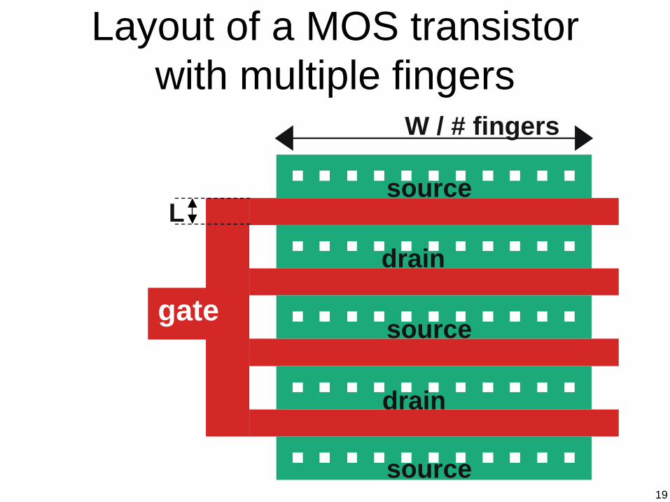
Layout of a MOS transistor with multiple fingers
source
drain
W / # fingers
gate
L
source
source
drain

20
Outline
• Introduction • Long-channel transistor • Small-geometry effects • Small-signal behavior at low frequencies • Capacitors and parasitic resistors • Evaluation of MOS performance in Matlab

21
MOS two-terminal structure
p-type Si (bulk)
gate oxide gate material
∞→L
induced channel not yet connected to the outside world
+ -
VGB
depletion zone induced channel
terminal 1
terminal 2
22
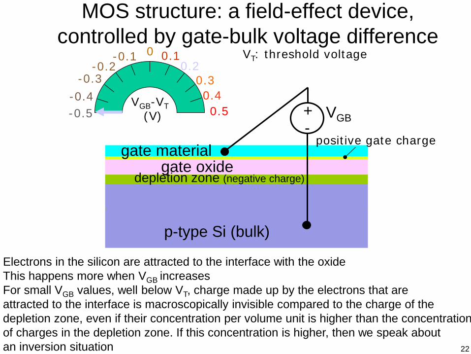
MOS structure: a field-effect device, controlled by gate-bulk voltage difference
p-type Si (bulk)
+ -
VGB
source n+
drain n+ gate oxide
positive gate charge
VGB-VT (V) -0.5
-0.4 -0.3
-0.2 -0.1 0 0.1
0.2 0.3 0.4 0.5
depletion zone (negative charge)
VT: threshold voltage
gate material
Electrons in the silicon are attracted to the interface with the oxide This happens more when VGB increases For small VGB values, well below VT, charge made up by the electrons that are attracted to the interface is macroscopically invisible compared to the charge of the depletion zone, even if their concentration per volume unit is higher than the concentration of charges in the depletion zone. If this concentration is higher, then we speak about an inversion situation

23
p-type Si (bulk)
+ -
VGB
source n+
drain n+ depletion zone gate oxide
positive gate charge
VGB-VT (V) -0.5
-0.4 -0.3
-0.2 -0.1 0 0.1
0.2 0.3 0.4 0.5
gate material
MOS structure: a field-effect device, controlled by gate-bulk voltage difference

24
p-type Si (bulk)
+ -
VGB
source n+
drain n+ depletion zone gate oxide
positive gate charge
VGB-VT (V) -0.5
-0.4 -0.3
-0.2 -0.1 0 0.1
0.2 0.3 0.4 0.5
gate material
MOS structure: a field-effect device, controlled by gate-bulk voltage difference

25
p-type Si (bulk)
+ -
VGB
source n+
drain n+ depletion zone gate oxide
positive gate charge
VGB-VT (V) -0.5
-0.4 -0.3
-0.2 -0.1 0 0.1
0.2 0.3 0.4 0.5
gate material
MOS structure: a field-effect device, controlled by gate-bulk voltage difference

26
p-type Si (bulk)
+ -
VGB
source n+
drain n+ gate oxide
positive gate charge
induced channel depletion zone
VGB-VT (V) -0.5
-0.4 -0.3
-0.2 -0.1 0 0.1
0.2 0.3 0.4 0.5
gate material
MOS structure: a field-effect device, controlled by gate-bulk voltage difference

27
p-type Si (bulk)
+ -
VGB
source n+
drain n+ gate oxide
positive gate charge
induced channel depletion zone
VGB-VT (V) -0.5
-0.4 -0.3
-0.2 -0.1 0 0.1
0.2 0.3 0.4 0.5
gate material
MOS structure: a field-effect device, controlled by gate-bulk voltage difference

28
p-type Si (bulk)
+ -
VGB
source n+
drain n+ depletion zone
gate oxide induced channel
VGB-VT (V) -0.5
-0.4 -0.3
-0.2 -0.1 0 0.1
0.2 0.3 0.4 0.5
positive gate charge gate material
MOS structure: a field-effect device, controlled by gate-bulk voltage difference

29
p-type Si (bulk)
+ -
VGB
source n+
drain n+ depletion zone
gate oxide induced channel
VGB-VT (V) -0.5
-0.4 -0.3
-0.2 -0.1 0 0.1
0.2 0.3 0.4 0.5
positive gate charge gate material
MOS structure: a field-effect device, controlled by gate-bulk voltage difference

30
p-type Si (bulk)
+ -
VGB
source n+
drain n+ depletion zone
gate oxide induced channel
VGB-VT (V) -0.5
-0.4 -0.3
-0.2 -0.1 0 0.1
0.2 0.3 0.4 0.5
positive gate charge gate material
MOS structure: a field-effect device, controlled by gate-bulk voltage difference

31
p-type Si (bulk)
+ -
VGB
source n+
drain n+ depletion zone
gate oxide induced channel
VGB-VT (V) -0.5
-0.4 -0.3
-0.2 -0.1 0 0.1
0.2 0.3 0.4 0.5
positive gate charge gate material
MOS structure: a field-effect device, controlled by gate-bulk voltage difference

32
p-type Si (bulk)
+ -
VGB
source n+
drain n+ depletion zone
gate oxide induced channel
VGB-VT (V) -0.5
-0.4 -0.3
-0.2 -0.1 0 0.1
0.2 0.3 0.4 0.5
positive gate charge gate material
MOS structure: a field-effect device, controlled by gate-bulk voltage difference

33
Drain-to-source voltage brings induced channel into movement: current!
p-type Si (bulk)
depletion zone
gate oxide
+ -
VDS > 0
source n+ n+
current
+ -
VGS=VGB-VSB
VGB-VT (V) -0.5
-0.4 -0.3
-0.2 -0.1 0 0.1
0.2 0.3 0.4 0.5
+ -
VGS
VSB
gate material
drain induced channel moving
positive gate charge

34
There are three inversion regimes: weak, moderate and strong inversion
• notation of inversion charge per unit area: Q’I • weak inversion:
– inversion charge macroscopically invisible compared to depletion charge
– Q’I increases exponentially with VGB
• strong inversion: – inversion charge clearly present, forms a well conducting strip
underneath the gate oxide, cfr. parallel-plate capacitance (C = Q/V or per unit area: C’ = Q’/V) Here: C’ox=Q’I/(VGB-VT) VT is the threshold that has to be surmounted by VGB to come into strong inversion
• Moderate inversion: – situation in between – Q’I dependence on VGB makes transition between exponential and
linear dependence

35
Expression of VT
000 Φ+Φ+= γFBT VV
VT0 decreases as oxide gets thinner (γ decreases) → easier gate control when oxide is thinner VT0 increases as doping level increases (γ and Φ0 increase) → VT0 can be adjusted with doping level NA (see next slide)
U times few a t+
⋅=Φ
i
At n
NU ln0
ox
ASi
CqN
'2ε
γ =
VFB: flat-band voltage
thermal voltage kT/q (25.8 mV at room temperature)
intrinsic concentration in Si (1.2 x 1010 cm-3)
subscript 0 means: VT without body bias (see also further)
acceptor concentration

36
VT is customized with ion implantations
without these implants |VT| would be too low
source drain
bulk
STI
gate
n+ n+ p
p
p
n- n-
poly Si
silicide silicide
silicide

37
VT implants cause large variability on VT for small downscaled devices
(over)simplified picture of a MOS
transistor
2016: Physical gate length = 9nm = 30x30x30 atoms
(22nm node)
2008: Physical gate length = 22nm (65nm node)
Courtesy: Asenov – TAD workshop at IMEC, 2005
• # atoms in channel of downscaled devices is not much anymore
• difference of a few atoms causes a visible shift of VT

38
Body effect counteracts the gate control
bulk (or body)
channel
+ - VCB
+ - VGC
depletion zone
source of free electrons used here to contact the channel to bring it on a certain voltage VCB
n+
oxide gate
wanted gate operation
Counteracting operation from the body
Channel affected by gate control and by body control
body effect is proportional to body effect coefficient γ → more pronounced for higher bulk doping → less pronounced for thinner oxide (gate is closer to channel,better gate control)
one finds: ( )000 Φ−+Φ⋅+= CBTT VVV γ
channel- bulk voltage

39
For VDS > 0 inversion level changes over the channel
p-type Si (bulk)
depletion zone
gate oxide
+ -
VDS > 0
source n+ n+
current
+ -
+ -
VGS
VSB
gate
drain
we assume that source side of the channel is strongly inverted The further you go in the channel into the direction of the drain, the higher the voltage difference VCB between a place in the channel and the bulk. → body effect is more pronounced as you move in the channel towards the drain → VT increases as you move towards the drain → inversion level decreases as you move towards the drain → the induced pn junction (p-side = bulk, n-side = inversion layer) is more inversely biased → thicker depletion zone
VCB

40
Terminology on inversion level and VT of a transistor
Inversion level of a transistor corresponds to inversion level at the source end
Inversion level at drain end is lower than at source end as soon as VDS > 0 V or, in other words, when VDB>VSB, there is more body effect at the drain end than at the source end “the VT of a transistor” corresponds to VT at the source end

41
Drain-to-source current as a function of VGS shows 3 inversion regimes
-0.5 -0.4 -0.3 -0.2 -0.1 0 0.1
-12
-11
-10
-9
-8
-7
-6
10
10
10
10
10
10
10
10 -5
VGS-VT
IDS (A)
almost quadratic dependence
0.2 -0.1 0 0.1 0.2 0.3 0.4 0.5 VGS (V) 0.6
leakage current when transistor is “off”
exponential dependence subthreshold slope ideally 60 mV/decade
=VT weak inversion moderate inversion strong inversion
data from 90nm process (IMEC) VT = 0.4 V

42
What is the boundary between the 3 inversion regimes ?
• weak – moderate: transition from exponential dependence of IDS on VGS to “non-exponential”
• moderate – strong: VOV = 0.2 V

43
Drain current IDS as a function of VDS
0 0.5 1 1.5 2 2.5 0
0.2
0.4
0.6
0.8
1
1.2
1.4 x 10 -3
VDS (V)
iDS (A)
VGS7> VGS6>… VGS1
VGS=VGS1
VGS=VGS2
VGS=VGS3
VGS=VGS4
VGS=VGS5
VGS=VGS6
VGS=VGS7
Increase of inversion level at source end

44
MOS is a controlled current source in the saturation region (VDS > VDSAT)
0 0.5 1 1.5 2 2.5 0
0.2
0.4
0.6
0.8
1
1.2
1.4 x 10 -3
VDS (V)
IDS (A)
: onset of saturation This occurs at VDS = VDSAT
Clearly, VDSAT is a function of VGS (at least in strong inversion)
saturation Nonsaturation or triode region
VGS7> VGS6>… VGS1
VGS=VGS1
VGS=VGS2
VGS=VGS3
VGS=VGS4
VGS=VGS5
VGS=VGS6
VGS=VGS7
saturation voltage

45
0 0.5 1 1.5 0
0.2
0.4
0.6
0.8
VDS (V)
IDS (A)
VGS=VGS1
VGS=VGS2
VGS=VGS3
VGS=VGS4
VGS=VGS5 At small VDS: VGS cannot increase the current, VGS can only change the slope of IDS(VDS)
slope for VGS4 = 1/rds0 for VGS4
VDS = 0V: MOS is a purely passive device, namely a voltage-controlled resistor with small-signal value rds0:
1
00
−
=
∂∂
=DSVDS
DSds V
Ir
MOS is a controlled resistor for small VDS
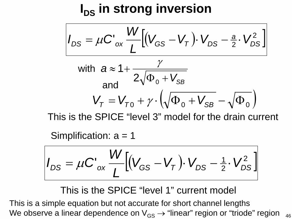
46
( )[ ]22' DSa
DSTGSoxDS VVVVL
WCI ⋅−⋅−= µ
IDS in strong inversion
This is the SPICE “level 3” model for the drain current
SBVa
+Φ+≈
021 γ
with
( )000 Φ−+Φ⋅+= SBTT VVV γand
( )[ ]221' DSDSTGSoxDS VVVV
LWCI ⋅−⋅−= µ
This is the SPICE “level 1” current model This is a simple equation but not accurate for short channel lengths We observe a linear dependence on VGS → “linear” region or “triode” region
Simplification: a = 1

47
Dependence of electric field on position in the channel (strong inversion)
Idrift(x) = µ W (-Q’I)E must be independent of x
we know that |Q’Isource|>|Q’Idrain|
Q’I is the inversion layer charge per unit area
Eat drain > Eat source
Ev ⋅= µ… we find that electrons at the drain end have a higher velocity than at the source end
Since

48
Saturation in strong inversion Physical interpretation: Drain end of the channel comes into weak inversion when VDB is increased
aVVV TGS
DSAT−
=
This happens at VDS = VDSAT
One finds in strong inversion:
for a =1, we find
VDSAT = VGS - VT

49
source drain
source drain
channel
source drain VDS2 = VDSAT
VDS3 > VDSAT
VDS4 > VDS3
gate oxide gate material
source drain VDS1 < VDSAT
channel
weak inversion moderate inversion strong inversion
Saturation of a MOS transistor (strong inversion) depletion layer
not shown for simplicity
channel
channel
legend in the channel:
gate oxide gate material
gate oxide gate material
gate oxide gate material

50
Physical interpretation of saturation in strong inversion
• saturation means: IDS does not change when VDS(which is assumed to
be > VDSAT) changes
• When part of the channel in the vicinity of the drain end is weakly
inverted, then this part of the channel can be represented as a very
poor conductor, almost an insulator (in which we can neglect the
presence of the electrons that form the drain current). Now, when the
drain voltage changes, which is at the right side of that insulator, then
at the left side of that insulator, nothing is “felt” of this change.

51
IDS in saturation, strong inversion: square-law model
Substitute VDS = VDSAT into eq. of IDS in triode region:
( )2
2' TGSoxDS VV
aLWCI −⋅= µ
square-law model
Shorthand notation, using the overdrive voltage VOV=VGS-VT:
2
2' OVoxDS V
aLWCI ⋅= µ

52
Incorrectness in the simplified model: electron velocity goes to ∞ at onset of saturation
Indeed, ( ) EQWII IdriftDS ⋅−⋅⋅== 'µ
goes to zero at VDS=VDSAT
this will then go to ∞ to have a nonzero IDS
v at drain end → ∞ This is physically impossible. We will correct this later
Ev ⋅= µ

53
Channel length modulation in strong inversion
gate oxide gate material
source drain channel
gate oxide gate material
source drain VDSAT
VDSAT
channel
L 1. Situation at VDS = VDSAT:
: saturation point
2. Situation for VDS > VDSAT:
Average horizontal electrical field in strongly inverted part of channel= VDSAT/L
driving force for drift current
VDS-VDSAT Average horizontal electrical field in strongly inverted part of channel= VDSAT/L’
L’<L
Driving force for drift current is now higher → more current

54
Due to Channel-Length Modulation (CLM), IDS depends on VDS
0 0.5 1 1.5 2 2.5 0
0.2
0.4
0.6
0.8
1
1.2
1.4 x 10 -3
VDS (V)
IDS (A)
saturation nonsaturation
VDSAT
current increases for VDS > VDSAT due to CLM
ideal current source behavior
( )DSV⋅+⋅ λ1
= (over)simplified SPICE level 1 model
= IDSAT . (1+λ. VDS)
( )2
2' TGSoxDS VV
aLWCI −⋅= µ

55
CLM less pronounced for longer channels
.. since decrease of channel length due to CLM is relatively less important for a longer channel → a longer transistor behaves as a more ideal current source than a short transistor (but it is slower, see later when we compute fT)

56
Zoom into weak and moderate inversion
0 0.5 1 1.5 2 2.5 10 -10
10 -9
10 -8
10 -7
10 -6
10 -5
10 -4
VGS=0V
VGS=0.1V
VGS=0.2V
VGS=0.3V
VGS=0.4V
VGS=0.5V
VT = 0.47V
In weak inversion we see: 1. vertical distance between curves is constant for the same ∆VGS
⇒ this corresponds to an exponential dependence of current on VGS 2. VDSAT is independent of VGS
weak inv. moderate inv.
VDS (V)
IDS (A)
Log scale
VDSAT in weak inv.

57
Weak inversion: negligible drift current
( )
−−⋅
∝
−
∝−∝
t
DS
t
GS
t
GD
t
GSIsourceIdraindiff
nUV
nUV
nUV
nUVQQI
exp1exp
expexp''
= 1 as soon as VDS > a few Ut ⇓ dependence on VDS vanishes → saturation
VDSAT in weak inversion is a few times Ut
Current mechanism is diffusion driving force is the gradient in concentration of inversion charge Q’I
weak inversion slope

58
Saturation of a MOS transistor in weak inversion
Physical interpretation: |Q’I| at drain decreases exponentially as VDB (or VDS) increases → inversion charge at drain is negligible as soon as VDS > a few times Ut
then the concentration gradient does not change anymore
0 L
|Q’I| |Q’I source|
|Q’I drain|
in saturation: |Q’I drain| << |Q’I source|
Q’I drain - Q’I source ≈ -Q’I source
Slope = driving force for diffusion current
IDS (proportional to Q’I drain - Q’I source ) does not change anymore with VDS
source end
drain end

59
Expression of IDS in weak inversion, long channel
−−
−⋅⋅
+⋅⋅=
t
DS
t
MGS2t
SBFoxDS U
Vexp1nU
VVexpUV2Φ2L
WC'μI γ
with VM = VT – a few times Ut (e.g. 6 Ut) and ΦF = Ut ln(NA/ni)

60
Note about the value of the weak inversion slope
• Weak inversion slope n is slightly dependent on bias and channel length
• For deep submicron processes it is around 1.4 … 1.2
• With downscaling it comes closer to one for long-channel devices

61
Drain current in moderate inversion
• Both diffusion and drift current are present • Dependence on VGS is in the transition between
exponential (weak inversion) and quadratic (strong inversion)
• A closed-form expression cannot be obtained for the current → iteration is required, but the form of the drain current is IDS = µ × C’ox × (W/L) × f(VGS, VDS, VSB)

62
Comparison of drift and diffusion current over the inversion levels
-12
-11
-10
-9
-8
-7
-6
-5
-4
-3
10
10
10
10
10
10
10
10
10
10
10 -2
diffusion drift
A
weak inversion (Idrift << Idiffusion) moderate inversion (Idrift ≈ Idiffusion) strong inversion (Idrift >> Idiffusion)
-0.5 -0.3 -0.1 0.1 0.3 0.5 0.7 0.9 1.1 1.3 VGS-VT (V) 0

63
Bias voltages are reduced to allow proper operation of downscaled CMOS
0
0.2
0.4
0.6
0.8
1
1.2
20406080100
[Vol
t]
Gate length [nm]
ITRS 2003
VT
VDD
VDD is scaled down to - prevent breakdown of gate oxide that is getting thinner with downscaling - limit the kinetic energy of electrons, that would damage the gate oxide (see also further)
To keep n-MOS in saturation: VDS > VGS − VT
hardly scales down
With downscaling it becomes more and more difficult to stack more than two transistors in saturation between the low VDD and ground
64
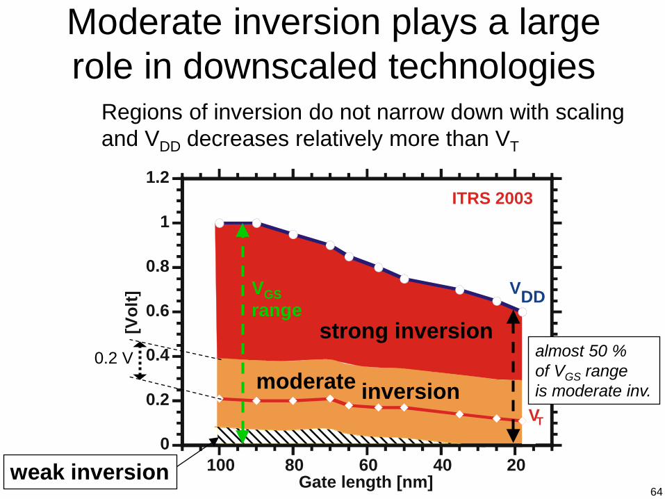
Moderate inversion plays a large role in downscaled technologies
Regions of inversion do not narrow down with scaling and VDD decreases relatively more than VT
0
0.2
0.4
0.6
0.8
1
1.2
20406080100
[Vol
t]
Gate length [nm]
ITRS 2003
VT
VDD
strong inversion
moderate inversion
weak inversion
almost 50 % of VGS range is moderate inv.
VGS range
0.2 V

65
In every inversion region IDS is proportional to µ.C’ox.(W/L)
In all regions of inversion we can write IDS = µ × C’ox × (W/L) × f(VGS, VDS, VSB)
cannot be chosen (fixed by technology)
design choice (determines the inversion level)
weaker dependence than on VGS, at least in saturation; guessed, or determined from the rest of the circuit
design choice
determined by specification on the current
IDS increases exponentially with VGS in weak inversion quadratically with VGSin strong inversion (saturation) transition between exp(VGS) and quadratic dependence in moderate inversion

66
Required width for a given current
From IDS = µ × C’ox × (W/L) × f(VGS, VDS, VSB) we find the required width for a given IDS:
µ × C’ox × f(VGS, VDS, VSB) IDS × L
W =
W decreases exponentially with increasing VGS in weak inversion quadratically with increasing VGS in strong inversion transition between exp(-VGS) and VGS
-2 dependence in moderate inversion

67
IDS(VGS) and W(VGS) for a given current
-0.6 -0.5 -0.4 -0.3 -0.2 -0.1 0 0.1 0.2 0.3 0.4 0.5 0.6 0.7 0.8 0.9 1 1.1 1.2 V OV (V)
-0.6 -0.5 -0.4 -0.3 -0.2 -0.1 0 0.1 0.2 0.3 0.4 0.5 0.6 0.7 0.8 0.9 1 1.1 1.2
10 -6
10 -4
10 -2
10 0
10 2
V OV (V)
W (m
)
iDS (A) 10-4
10-6
10-8
10-10
10-12
the lower the inversion level, the wider a transistor needs to be to conduct a specified IDS
drain current for a given width
width for a given drain current
IDS = µ × C’ox × (W/L) × f(VGS, VDS, VSB)
µ × C’ox × f(VGS, VDS, VSB)
IDS × L W =

68
Sizing of a MOS transistor based on a specification for the current
1. typically, we choose L 2. next we choose the inversion level 3. based on the current for a given
reference width and the current spec, we find the width for the transistor
the lower the inversion level, the wider the transistor will be

69
Outline
• Introduction • Long-channel transistor • Small-geometry effects • Small-signal behavior at low frequencies • Capacitors and parasitic resistors • Evaluation of MOS performance in Matlab

70
Small-dimension effects
• Long and wide channels: This is no longer true for short and narrow channels short-channel and narrow-channel effects
• Gate oxide gets thinner with downscaling thin gate oxide effects
WIDS ∝
LIDS
1∝ (if we neglect CLM)

71
Classification of most important small-geometry effects
Thin gate oxide effects: - mobility degradation due to vertical electrical field - poly gate depletion - gate leakage Short channel effects: - velocity saturation - drain-induced barrier lowering - impact ionization (not treated here) Narrow channel effect: see slides further

72
Mobility degradation due to vertical electrical field
gate oxide gate material
channel Ey
Ex source drain
Electric field that acts on electrons in the channel has 2 components: - Horizontal field Ex (“drift field”) - Vertical field Ey (due to gate operation, see 2-terminal structure) → electrons are accelerated not exactly horizontally, but also slightly vertically → electrons want to enter the gate oxide, but this is impossible → they undergo more collisions This is modeled by a degradation of the mobility

73
Simplified modeling of mobility degradation
in strong inversion:
( )TGSeff VV −⋅+
=θ
µµ1
0
More mobility degradation for higher gate overdrive (logical, since then the vertical electric field is higher)
θ proportional to 1/tox
< µ0

74
Velocity saturation Absolute value of the velocity of electrons in Si is about 105 m/s at room temperature. This is called the saturation velocity vsat
low horizontal electrical field Ex Ex opposite to x direction
x x Average velocity in x direction = 0
zero electrical field
Average velocity in x direction = µ E << vsat
(averaged over many electrons)
velocity vector of an electron
source
drain

75
Velocity saturation (continued) At high horizontal electrical fields Ex average
velocity cannot be higher than vsat
Then v is no longer proportional to E
105 106 107 108103
104
105 v (m/s)
E (V/m) EC
EC: “critical electrical field”
v =µ E

76
Velocity saturation causes a decrease of IDS
One can derive an approximate expression for IDS in strong inversion, nonsaturation:
( )[ ]
C
DSDSDSTGSoxeffDS
ELVVaVVV
LWCI
⋅+
⋅⋅−⋅−⋅⋅⋅=1
1' 21µ
< 1 with EC=vsat/µeff “critical electrical field” Velocity saturation
more severe as L decreases
Velocity saturation plays a larger role than mobility reduction

77
Combination of mobility degradation and velocity saturation into one
model (strong inversion)
( ) ( )
C
DSATTGSox
TGSDSAT
ELVVV
aLWC
VVI
⋅+
⋅−⋅⋅⋅−⋅+
=1
12
'1
20
θµ
Strong inversion (VOV ≥ 0.2 V), triode region:
Strong inversion (VOV ≥ 0.2 V), saturation region:
( ) ( )[ ]
C
DSDSDSTGSox
TGSDS
ELVVaVVV
LWC
VVI
⋅+
⋅⋅−⋅−⋅⋅⋅−⋅+
=1
1'1 2
10
θµ
Note: velocity saturation is usually more important than mobility degradation
(1)

78
Further simplification in saturation
( ) ( )
C
DSATTGSox
TGSDSAT
ELVVV
aLWC
VVI
⋅+
⋅−⋅⋅⋅−⋅+
=1
12
'1
20
θµ
x+11both of the form
yxyx ++≈
+⋅
+ 11
11
11using
and VDSAT ≈ VGS-VT and EC≈vsat/µ0
( )( )2
0
0
2'
1TGSox
TGSsat
DSAT VVaL
WCVV
Lv
I −⋅⋅⋅−⋅
⋅
++=
µθ
µwe find from eq. (1) on previous slide
eq. (60):

79
For very short channels, deep strong inversion: MOS in saturation becomes
a linear device
( ) 10 >>+−⋅⋅
θµTGS
sat
VVLv
if
( )TGSoxsat
DSAT VVa
CvWI −⋅⋅⋅
≈2
'
IDSAT linearly dependent on VGS – VT !! → gm becomes independent of VGS - VT
80
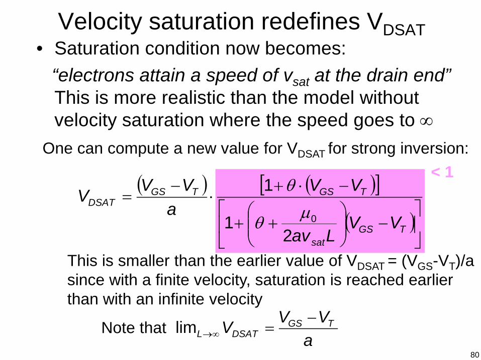
Velocity saturation redefines VDSAT • Saturation condition now becomes: “electrons attain a speed of vsat at the drain end”
This is more realistic than the model without velocity saturation where the speed goes to ∞
One can compute a new value for VDSAT for strong inversion:
( ) ( )[ ]
( )
−
++
−⋅+⋅
−=
TGSsat
TGSTGSDSAT
VVLav
VVa
VVV
21
1
0µθ
θ
This is smaller than the earlier value of VDSAT = (VGS-VT)/a since with a finite velocity, saturation is reached earlier than with an infinite velocity
aVVV TGS
DSATL−
=∞→limNote that
< 1

81
Hot electrons: electrons with saturation velocity
vsat
source drain
Electron speed in the channel (qualitatively)
Hot electrons at drain end have high kinetic energy (mv2/2): - they collide with atoms, hereby generating new electron/hole pairs - they can enter the gate oxide under influence of the vertical electric field
This can be destructive for a transistor

82
Effect of hot electrons is lowered using lowly-doped drain (LDD) regions
source drain
oxide
gate
n+ n+ p
p
p
n- n-
poly Si
silicide silicide
silicide
LDD regions: lowly doped, hence highly resistive → voltage drop IDS R decreases voltage drop over the channel → horizontal electrical field decreases
R R IDS

83
Drain-induced barrier Lowering (DIBL)
Barrier (for inversion) is lowered thanks to the fact that the space charge layers (- - -), which are present by the source-bulk and drain bulk p-n junctions, intersect with the zone that needs to be depleted before we have a channel

84
DIBL (continued)
: intersection region; this is already depleted by presence of p-n junction of source/bulk and drain/bulk
Situation at VDS = 0V
The intersection region is relatively important for short channels → Gate action does not have to deplete anymore the intersection region → “barrier (for inversion) is lowered”

85
DIBL (continued 2)
Situation at VDS > 0V
Intersection region is larger at the drain side for VDS > 0V This explains the name ‘drain-induced’ for this effect The channel is now not only controlled by the gate voltage, but also by the drain voltage
DIBL: more pronounced for shorter channels, less pronounced if gate oxide is thinner (gate is closer to the channel, yielding better gate control)

86
DIBL is limited with pocket implants
source drain tox
oxide
gate
n+ n+ p
p
p
n- n-
poly Si
silicide silicide
silicide
pocket implants (also called “halo implants”) = highly doped regions into which the extension of the space charge layer of the source-bulk (drain-bulk) diode is kept limited

87
DIBL is modeled by making VT dependent on L and VDS
0
0.1
0.2
0.3
0.4
0.5
L (normalized to Lmin) 1 10
VT (V)
without pocket implants (qualitatively)
with pocket implants
0 0.2 0.4 0.6 0.8 1 1.2 1.4 1.6 1.8 0.34
0.36 0.38
0.4
0.42
0.44 0.46
0.48 0.5
0.52
0.54
VDS (V)
VT (V)
L=0.18µm
L=2µm
data for 0.18 µm CMOS
For long channels: dependence of VT on L and VDS is small
DST VLV ⋅−∆ )(~ σσ: DIBL coefficient (> 0)

88
DIBL is a serious scaling problem • Drain-source voltage starts to control the
channel One of the causes of increased leakage current at VGS
= 0 V:
• Can be reduced by making the influence of the gate on the channel stronger – Thinner gate oxide (gate is closer to the channel)
• Problem: gate oxide downscaling causes more and more gate leakage
– Multi-gate devices (e.g. FinFETs)
−∝
t
DSTGSDS nU
)(VVVexpI decrease of VT due to DIBL at VGS=0 V yields exp. increase of IDS

89
Slope of IDS versus VDS in saturation is determined both by CLM and DIBL
For VDS > VDSAT: small VDS values: CLM dominates over DIBL larger VDS values: DIBL dominates over CLM
Both effects become less important as channel length increases → IDS-VDS curves are flatter for longer transistors than for short ones

90
Narrow-channel effect causes decrease of VT
oxidetrench
oxidetrench
W
fringingfield
gateoxide
Extra “fringing” field lines contribute to depletion of the channel, while they have not been taken into account previously → gate operation more efficient than previously calculated This is quantified by a lower VT
gate
Si bulk

91
Narrow-channel effect is modeled by making VT dependent on W
0.2
0.25
0.3
0.35
0.4
0.45
0.5V
T (Vol
t)
W (micrometer)0.3 1.0 10
Narrow-channel effect negligible for W > 2 µm in this technology
0.18 µm CMOS
in 0.18 µm CMOS: IDS is linearly dependent on W for W > 2 µm
L = 0.18 µm
L = 2 µm

92
Poly-gate depletion decreases IDS
depletion zone
tox
n-type polysilicon depleted zone in n-type polysilicon
Similar for p-MOS structure
Gate stack for n-MOS:
silicided polysilicon
inversion layer
higher effective tox lower C’ox lower IDS
effect is not present for metal gate
= extra insulating layer that adds to oxide layer
In doped polysilicon the free carriers can move under the influence of a potential difference, just as in crystalline silicon, leaving behind a depleted zone

93
Gate leakage current caused by thin gate oxide
• tox decreases with downscaling – nowadays gate oxide is just a few atomic layers thick
→ leaky gate oxide → “direct tunneling” current of electrons through oxide → current density ~ exp(-tox)
• Further downscaling involves use of high-k oxides with ε (= k) > εSiO2 → “effective oxide thickness” (EOT) < physical tox e.g. 90 nm CMOS: SiON gate oxide, tox= 2 nm, EOT = 1.5 nm

94
Gate leakage current flows into source (IGS), drain (IGD) and bulk (IGB)
gate-to-channel current IGC is split over source and drain IGS = IGCS + IGSO IGD = IGCD + IGDO
IGCS IGCD
IGB
IGDO IGSO
IGC

95
Gate leakage for 90 nm
|IGD| (A)
VDS (V) 0 0.2 0.4 0.6 0.8 1 1.2 10 -13
10 -12
10 -11
10 -10
10 -9
90 nm CMOS W = 10 µm L = 90 nm n-MOS with VGS = 0 V

96
Evaluation of IDS in 0.18 µm CMOS (1)
0 0.2 0.4 0.6 0.8 1 1.2 1.4 1.6 1.80
0.5
1
1.5x 10⁻³
|VDS (V)|
i DS (A
)
iDS (VSB = 0 V, W = 10µm, n-MOS of UMC CMOS 180 nm)VGS=0.20
VGS=0.30
VGS=0.40
VGS=0.50
VGS=0.60
VGS=0.70
VGS=0.80
VGS=0.90
L = 0.18 µm, W/L = 10/0.18
Note: VT0 ≈ 0.5 V

97
Evaluation of IDS in 0.18 µm CMOS (2)
0 0.2 0.4 0.6 0.8 1 1.2 1.4 1.6 1.80
0.5
1
1.5
2
2.5 x 10⁻³
|VDS (V)|
i DS (A
)
iDS (VSB = 0 V, W = 200µm, n-MOS of UMC CMOS 180 nm)
VGS=0.20VGS=0.30VGS=0.40VGS=0.50VGS=0.60VGS=0.70VGS=0.80VGS=0.90
Longer channel → flatter curves in saturation larger current than for L=0.18µm due to less velocity saturation
L = 4 µm, W/L = 10/0.18

98
Evaluation of IDS in 0.18 µm CMOS (3) L = 0.18 µm, W/L = 10/0.18
0 0.2 0.4 0.6 0.8 1 1.2 1.4 1.6 1.810-12
10-10
10-8
10-6
10-4
10-2
straight line = exp. behavior (weak inversion)
VGS (V)
IDS (A) (log. scale)
Note: VT0 ≈ 0.5 V

99
Evaluation of VDSAT in 0.18 µm CMOS
-0.4 -0.2 0 0.2 0.4 0.6 0.8 1 1.2
0.2
0.4
0.6
0.8
1
1.2
|VGS - VT| (V)
|VD
SA
T| (V
)
|VDSAT|(n-MOS of UMC CMOS 180 nm, VSB = 0 V, VDS = 0.9 V)
L =180.00nmL =885.00nmL =1.59µmL =2.29µmL =3.00µmVOV
level 1: VGS-VT
a few Ut in weak inversion
far below VGS-VT due to velocity sat.
45° Long channel slope < 1 since a > 1

100

101
Outline
• Introduction • Long-channel transistor • Small-geometry effects • Small-signal equivalent circuit at low
frequencies • Capacitors and parasitic resistors • Evaluation of MOS performance in Matlab

102
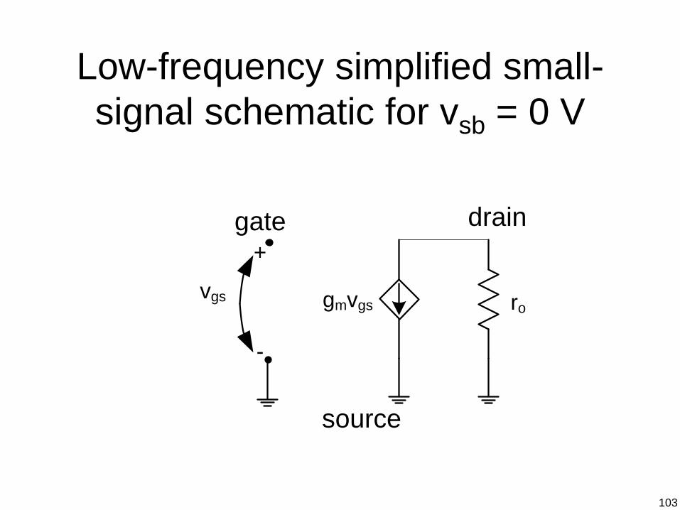
Small-signal schematic of a MOS transistor at low frequencies
iDS = f(vGS, vDS, vSB) = IDS + ids ids = gm.vgs + go.vds – gmb.vsb
DC AC, small-signal
GS
DSm v
ig∂∂
=DS
DS
vig
∂∂
=0SB
DSmb v
ig∂∂
−== 1/ro=1/rds=gds
with vGS = VGS + vgs
vDS = VDS + vds
vSB = VSB + vsb
gm.vgs gmb
.vsb go
G
S
D
B
103
Low-frequency simplified small-signal schematic for vsb = 0 V
gate
source
drain
gmvgs ro
+
-
vgs
104
0 0.5 1 1.5 2 2.5 0
0.2
0.4
0.6
0.8
At VDS = 0 V: gm = 0, go ≠ 0 regardless of the inversion region
gate
source
drain
gmvin rovin
VDS (V)
IDS (A)
VGS=VGS1
VGS=VGS2
VGS=VGS3
VGS=VGS4
At VDS = 0V: IDS = 0 for any VGS → ∂IDS/ ∂VGS= 0 → gm=0
Small-signal equivalent circuit:

105
gm in strong inversion, triode region
From level 3 expression of IDS :
( )[ ]
DSox
DSa
DSTGSoxGSGS
DSm
VL
WC
VVVVL
WCVV
Ig
⋅=
⋅−⋅−
∂∂
=∂∂
=
'
' 22
µ
µ
gm is linearly proportional to W/L
gm=0 when VDS = 0 → no active circuit anymore
This is only an approximation (for VOV ≥ 0.2V), but trends remain valid:

106
gm in strong inversion, saturation ( )
( ) OVoxTGSox
TGSoxGSGS
DSm
VaLWCVV
aLWC
VVaL
WCVV
Ig
⋅=−⋅=
−⋅
∂∂
=∂∂
=
''
2' 2
µµ
µ
only approximately valid for VOV ≥ 0.2 V
DSox
OV
DSm
IaLWC
VIg
'2
2
µ=
=
Eq. (1) can be reworked to
(1)
(2)
long-channel approximation
(3)

107
gm/IDS in strong inversion, saturation
from eq. (2):
OVDS
m
VIg 2
= (for VOV ≥ 0.2 V)
The further in stronger inversion, the less economical the transistor operates, since more current is required for a given gm
At the edge of strong inversion: Vov = 0.2 V → gm/IDS = 10 V-1
e.g. : we need a gm of 1 mS → at VOV= 0.2 V we need a current of ≈ 0.1 mA
108
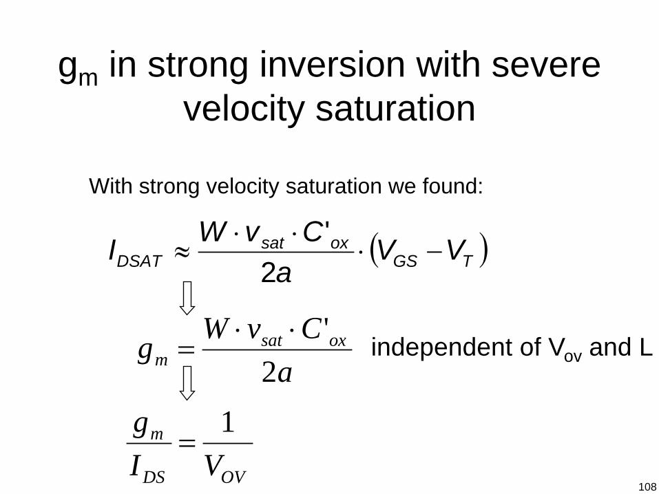
gm in strong inversion with severe velocity saturation
With strong velocity saturation we found:
aCvWg oxsat
m 2'⋅⋅
= independent of Vov and L
( )TGSoxsat
DSAT VVa
CvWI −⋅⋅⋅
≈2
'
OVDS
m
VIg 1
=

109
gm and gm/IDS in weak inversion
tDS
m
t
GS
tm
t
GSDS
nUIg
nUV
nUg
nUVI
1
exp1
exp
=
⇓
∝
⇓
∝
GSDSm VIg ∂∂= /

110
gm/IDS is maximal in weak inversion
strong inversion (VOV ≥ 0.2 V):
weak inversion: tDS
m
nUIg 1
=
maximum value is 10 (for VOV = 0.2 V)
close to 30 (for n = 1.3)
OVDS
m
VIg 2
=
moderate inversion: transition between weak inversion value and 2/VOV

111
gm increases with the inversion level
-12
-10
-8
-6
-4
10
10
10
10
10 -2
-0.6 -0.4 -0.2 0 0.2 0.4 0.6 0.8 1 1.2 10 V OV (V)
g m (S
)
long-channel transistor

112
… but gm/IDS decreases with increasing inversion level
V OV (V) -0.6 -0.4 -0.2 0 0.2 0.4 0.6 0.8 1 1.2 10
0
10 1
g m /I D
S (V
-1 )
almost constant in weak inversion
proportional to Vov-1 in
strong inversion
long-channel transistor

113
Required width for a given gm ),,(' SBDSGSoxDS VVVf
LWCI µ=
GSoxm V
fL
WCg∂∂
= 'µ
W decreases exponentially with increasing VGS in weak inversion and with VGS
-1 in strong inversion;
transition between exp(-VGS) and VGS-1 dependence in moderate inversion
we know that
f: increases exponentially with VGS in weak inversion; increases quadratically with VGS in strong inversion; transition from exponential to quadratic in moderate inversion
GSox
specifiedm
VfC
Lg
∂∂
='µ
Wrequired
∂f/∂VGS: increases exponentially with VGS in weak inversion; increases linearly with VGS in strong inversion; transition from exponential to linear in moderate inversion
just as with the sizing of a transistor for a specified current, we see that the required W to realize a given gm decreases when the inversion level increases
114
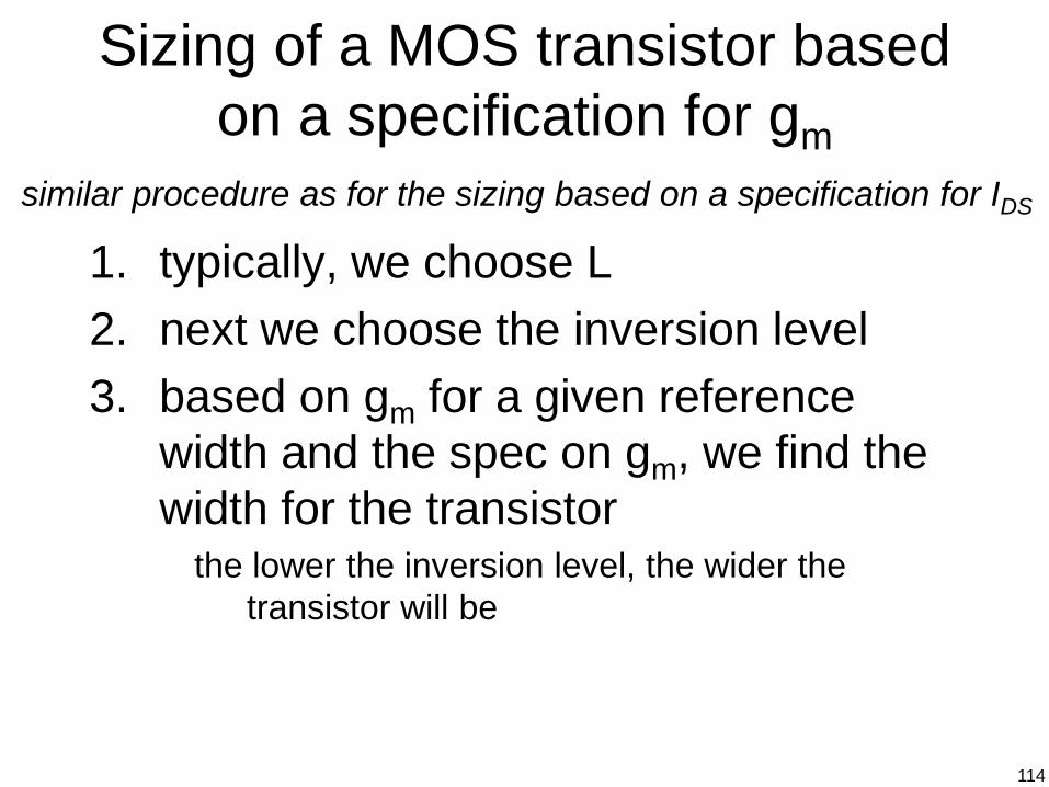
Sizing of a MOS transistor based on a specification for gm
1. typically, we choose L 2. next we choose the inversion level 3. based on gm for a given reference
width and the spec on gm, we find the width for the transistor
the lower the inversion level, the wider the transistor will be
similar procedure as for the sizing based on a specification for IDS

115
Evaluation of gm/IDS in 0.18 µm CMOS
-0.5 0 0.5 1 1.50
5
10
15
20
25
30
35
40
VGS - VT (V)
g m/I D
S (
V-1
)
gm/IDS(n-MOS of UMC CMOS 180 nm, VSB = 0 V, VDS = 0.9 V)
L =180nmL = 2.00µm
weak inv. max. and constant
/I
strong inv.
mod. inv.
Difference due to nshort channel > nlong channel

116
Study of go • Large in the triode region • Much smaller in saturation
• Nonzero due to CLM and DIBL • Dependent both on VGS and VDS
• can be decreased by increasing the channel length
0 0.2 0.4 0.6 0.8 1 1.2 1.4 1.6 1.80
0.5
1
1.5
2
2.5
3x 10⁻⁷
VDS (V)
g o (A/V
)
go (VSB = 0 V, W = 10µm, L = 0.18µm, n-MOS of UMC CMOS 180 nm)
VGS=0.20
saturation

117
Value of go at VDS= 0 V in strong inversion
( )[ ]
( )TGSox
DSa
DSTGSoxDSDS
DS
VVL
WCg
VVVVL
WCVV
Ig
−⋅=
=
⋅−⋅−
∂∂
=∂∂
=
'
:V 0Vfor
'
0
DS
220
µ
µ
This is the same expression as for gm in strong inversion, saturation We will use that when we will calculate the thermal noise from a MOS transistor.

118
gm/go is the intrinsic gain of the transistor
RL
VDD
vout
vin
M1
maximum voltage gain vout/vin is obtained for RL→∞ This max. voltage gain is called the intrinsic gain
vin gm vin go
voutgate
source, bulk
drain
small-signal circuit for RL →∞:
o
m
in
out
gg
vv gain intrinsic ==
LR/1gg
vv
o
m
in
out
+−=

119
Evaluation of gm/go in 0.18 µm CMOS
0 0.2 0.4 0.6 0.8 1 1.2 1.4 1.60
5
10
15
20
25
30
35
VDS (V)
g m/g
o (-)
gm/go (VSB = 0 V, W = 10µm, L = 0.18µm, n-MOS of UMC CMOS 180 nm)
VGS=0.20VGS=0.30VGS=0.40VGS=0.50VGS=0.60VGS=0.70VGS=0.80VGS=0.90
note: VT0 ≈ 0.5 V

120
gm/go decreases with downscaling Channels become shorter → DIBL and CLM are more pronounced
Technology node
(gm/go)max
for Lmin (n-MOS) 180 nm 25 - 30 90 nm 10 - 15 65 nm and beyond
< 10
VDS=1.2 V
VDS=0.6 V
e.g. 90 nm CMOS n-MOS W=10 µm, L = 90 nm
0
5
10
15
20
0.4 0.6 0.8 1.0 1.2
measured modeled
gm/go
VGS (V)

121
Bulk transconductance gmb < gm
0.2 0.4 0.6 0.8 1 1.2 1.4 1.6
6.4
6.5
6.6
6.7
6.8
6.9
7
7.1
VDS (V)
g m/g
mb (-
)gm/gmb (VSB = 0 V, W = 10µm, L = 0.18µm, n-MOS of UMC CMOS 180 nm)
VGS=0.20
VGS=0.30
VGS=0.40
VGS=0.50
VGS=0.60
VGS=0.70
VGS=0.80
VGS=0.90
gm/gmb= 6 to 7 → in this 0.18 µm technology, gate control is 6 – 7 times stronger than body control This ratio tends to increase with downscaling
note: VT0 ≈ 0.5 V

122

123
Outline
• Introduction • Long-channel transistor • Small-geometry effects • Small-signal equivalent circuit at low
frequencies • Capacitors and parasitic resistors • Evaluation of MOS performance in Matlab

124
Capacitors in a MOS transistor
• Associated to charge storage small-signal operation: C = |∆q/∆v|=|∂Q/∂V|
• Intrinsic capacitors
= capacitors that depend on the physical operation of a MOS transistor, without taking into account its connection to the outside world and inevitable structures due to fabrication
• Extrinsic capacitors
= capacitors that only depend on the connection of the transistor to the outside world and on inevitable structures due to fabrication
125
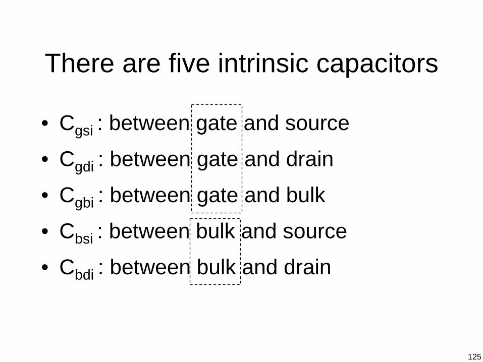
There are five intrinsic capacitors
• Cgsi : between gate and source
• Cgdi : between gate and drain
• Cgbi : between gate and bulk
• Cbsi : between bulk and source
• Cbdi : between bulk and drain

126
Measurement of intrinsic capacitors strong inversion situation nonsaturation
QI + QB + QG (+ Qox) = 0 (charge neutrality) not shown
We will apply a ∆V and measure the resulting ∆Q at gate and bulk
+ −
S D
B
gate oxide + + + + + + + + + +
G QI
− − −
− −
− − −
− −
− −
QG
QB
− − − − − − − − − − − − − − − − − − − − − − − − −
+ −
+ −
+ −
VB VS
VD
VG
x=0 x=L
dxxQWQL
GG )(0
'∫=
dxxQWQL
BB )(0
'∫=
Note that
We will not elaborate the expressions of QG and QB

127
Applying ∆VS identifies Cgsi …
+ −
S D
B
gate oxide + + + + + + + + + +
G QI
− − −
− −
− − −
− −
− −
QG
QB
− − − − − − − − − − − − − − − − − − − − − − − − −
+ −
+ −
+ −
VB VS
VD
VG
VS with constant VG ΨOXIDE QG
BDG VVVS
Ggsi V
QC,,∂
∂−=
+ −
S D
B
gate oxide + + + + + + + + + +
G QI
− − − −
− −
− −
− −
− −
QG
QB
− − − − − − − − − − − − − − − − − − − −
+ −
+ −
+ −
VB VS
VD
VG
+∆VS
+∆QG
+∆QB
− − − − −
−

128
… and Cbsi
+ −
S D
B
gate oxide + + + + + + + + + +
G QI
− − −
− −
− − −
− −
− −
QG
QB
− − − − − − − − − − − − − − − − − − − − − − − − −
+ −
+ −
+ −
VB VS
VD
VG
VS with constant VB depletion zone extends (at least in mod. and strong inv.) QB more negative
BDG VVVS
Bbsi V
QC,,∂
∂−=
+ −
S D
B
gate oxide + + + + + + + + + +
G QI
− − − −
− −
− −
− −
− −
QG
QB
− − − − − − − − − − − − − − − − − − − −
+ −
+ −
+ −
VB VS
VD
VG
+∆VS
+∆QG
+∆QB
− − − − −
−

129
Definition of Cgdi, Cbdi and Cgbi
• Cgdi and Cbdi are similar to Cgsi and Cbsi:
• Cgbi: VB depletion zone narrows QB less negative QG decreases
and
BSG VVVD
Bbdi V
QC,,∂
∂−=
BSG VVVD
Ggdi V
QC,,∂
∂−=
DSG VVVB
Ggbi V
QC,,∂
∂−=

130
Expressions of intrinsic capacitances in strong inversion, VDS = 0
QI
QG
QB S
B
gate oxide + + + + + + + + + +
G
− −
− −
− −
− −
− −
− −
WLCC oxgsi'
21
= WLCCC bcbdibsi'
21
==
0=gbiCCox equally divided between source and drain bulk is invisible due to
shielding by inversion layer
long channel
−
WLCC oxgdi'
21
=
'bcC : capacitance per unit area of the reverse
biased field-induced junction formed by the inversion layer and the substrate:
'
0
'
2 oxSB
bc CV
C+Φ
=γ
D

131
Expressions of intrinsic capacitances in strong inversion, saturation
QI
QG
QB
S
B
gate oxide + + + + + + + + + +
G
− − −
− −
− − −
− −
− − − − −
WLCC oxgsi'
32
=
0=gdiC 0=bdiC
WLCC bcbsi'
32
=
aaC
CCWLCC ox
ox
bc
bcgbi 3
1
13 '
'
' −=
+
=
< Cox !!
∆VD has no influence on QG and QB
< Cbc
> 0 since bulk is visible at drain side, due to absence of inversion layer there
long channel
D

132
Expressions of intrinsic capacitances in weak inversion, saturation
0=gsiC
0=gdiC 0=bdiC
0=bsiC
bulk - channelC with series in WLCC oxgbi'=
QI macroscopically
invisible
QG
QB S
B
gate oxide + + + + + + + + + +
G
− −
− −
− −
− −
− −
− −
long channel
− D − − − − − −
→ in weak inversion: the only intrinsic capacitance is Cgbi

133
Extrinsic capacitors • Extrinsic capacitors
– Proportional to W, expressed per unit width - between gate and source (Cgso × W) - between gate and drain (Cgdo × W) • Junction capacitors
– depend on layout - between source and bulk (Cjs) - between drain and bulk (Cjd)
[F/m]
[F/m]

134
source
tox
gate
n- n-
poly Si
silicide
silicide
COV: overlap capacitance
Ctop
Cof: outer fringing capacitance
3
1
2
n+
They have 3 components, each proportional to W
Extrinsic parts of Cgs and Cgd: Cgso and
Cgdo

135
Total Cgs and Cgd: sum of intrinsic and extrinsic parts
• Cgs = Cgsi + Cgso • Cgd = Cgdi + Cgdo

136
Cbs and Cbd have intrinsic and extrinsic part
Cbs = Cjs + Cbsi
Cbd = Cjd + Cbdi
Usually: Cjs >> Cbsi
junction capacitance
intrinsic (see previous slides)
junction capacitance
intrinsic (see previous slides)
Cjd >> Cbdi
Junction capacitors dominate intrinsic source-bulk and drain-bulk capacitors

137
Extrinsic source-bulk and drain-bulk capacitors have bottom plate and sidewall components
source drain tox
bulk
STI
gate
n+ n+ p
p
p
n-
poly Si
silicide silicide
silicide
STI
Cjswg
Cjsw Cj
Cj: bottom plate capacitance (F/m2) Cjsw: sidewall capacitance (F/m) Cjswg: sidewall capacitance (F/m) at gate side

138
Sidewall capacitances are proportional to perimeter of source/drain regions
source source drain drain
lsos lsos lsogd lsogs lsogd
lsos: length of the source diffusion not between 2 poly stripes lsogs: length of the source diffusion between 2 poly stripes lsod: length of the drain diffusion not between 2 poly stripes (not present in this picture) lsogd: length of the drain diffusion between 2 poly stripes
ps: perimeter of the source enclosed by STI
psg: perimeter of the source at the gate side
pd: perimeter of the drain enclosed by STI
pdg: perimeter of the drain at the gate side
source ga
te
gate
gate
gate
These distances are determined by the layout rules

139
Bottom plate capacitances are proportional to area of source/drain regions
as: area of source region
source source drain drain source
ad: area of drain region
gate
gate
gate
gate

140
Total extrinsic source-bulk capacitance
psgCpsCasC jswgjswj ⋅+⋅+⋅=jsC
depend on VSB, since these are junction capacitances
mj
j
inverse
Vjunction
junction
VV
CC inverse
+
= =
1
0
General expression for a junction capacitance:
Vj: junction potential (0.2 … 0.9 V) mj: grading coefficient (0.3 … 0.5)

141
Total extrinsic drain-bulk capacitance
pdgCpdCadC jswgjswj ⋅+⋅+⋅=jdC
Similar to Cjs:

142
Evaluation of Cgs in 0.18 µm CMOS
0 0.2 0.4 0.6 0.8 1 1.2 1.4 1.6 1.80
0.2
0.4
0.6
0.8
1
VGS (V)
Cgs
/(C' ox
×W×L
)
normalized Cgs VSB = 0 V, L = 0.18µm,n-MOS of UMC CMOS 180 nm, C'ox = 8.21fF/µm2
VDS=0.00
VDS=0.45
VDS=0.90
VDS=1.35
VDS=1.80
weak inversion: only extrinsic
strong inversion, saturation: extrinsic + 2/3 C’ox WL
triode region
VT

143
0 0.2 0.4 0.6 0.8 1 1.2 1.4 1.6 1.8 2
0
0.2
0.4
0.6
0.8
1
VGS (V)
Cgd
/(C' ox
×W×L
)
normalized Cgd VSB = 0 V, L = 0.18µm,n-MOS of UMC CMOS 180 nm, C'ox = 8.21fF/µm2
VDS=0.00
VDS=0.45
VDS=0.90
VDS=1.35
VDS=1.80
Evaluation of Cgd in 0.18 µm CMOS
weak inversion: only extrinsic strong inversion, saturation:
only extrinsic
triode region
VT
144
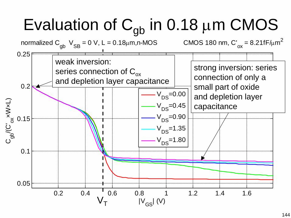
0.2 0.4 0.6 0.8 1 1.2 1.4 1.60.05
0.1
0.15
0.2
0.25
|VGS| (V)
Cgb
/(C' ox
×W×L
)
normalized Cgb VSB = 0 V, L = 0.18µm,n-MOS of UMC CMOS 180 nm, C'ox = 8.21fF/µm2
VDS=0.00
VDS=0.45
VDS=0.90
VDS=1.35
VDS=1.80
Evaluation of Cgb in 0.18 µm CMOS
VT
weak inversion: series connection of Cox and depletion layer capacitance
strong inversion: series connection of only a small part of oxide and depletion layer capacitance
145
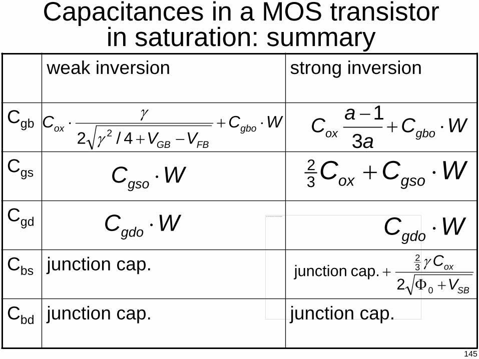
Capacitances in a MOS transistor in saturation: summary
weak inversion strong inversion
Cgb
Cgs
Cgd
Cbs junction cap.
Cbd junction cap. junction cap.
WCVV
C gbo
FBGB
ox ⋅+−+
⋅4/2 2γ
γ
SB
ox
VC+Φ
+0
32
2 cap. junction
γ
This image cannot currently be displayed.
WCa
aC gboox ⋅+−
31
WCC gsoox ⋅+32
WCgdo ⋅
WCgso ⋅
WCgdo ⋅

146
Speed of a MOS transistor is expressed with cutoff frequency fT
Cutoff frequency fT = frequency at which the current gain of a MOS transistor has dropped to an absolute value of 1
∆
Cgs+Cgb
Cgd1
gm v1Iin
iout
ACshortcircuit
( )gbgdgs
m
in
out
CCCg
ii
++≈
ωcurrent gain:
Cgg

147
Expression for fT
gg
mT
gg
m
gg
m
Cgf
Cgf
Cfg
πππ 2
2 for 1
2=⇒==
fT depends on gm and hence on Vov:
-0.4 -0.2 0 0.2 0.4 0.6 0.8 1 1.2 1.4104
106
108
1010
1012
VGS - VT (V)
f T (Hz)
180 nm CMOS: fT in the vicinity of 60 GHz
Vov (V)

148
fT increases when L decreases
223
2 aLVf OV
T πµ≈
Strong inversion, saturation:
LWCCCVaLWCg oxgsggOVoxm ⋅⋅≈≈⋅= '' 3
2 and µ
with strong velocity saturation, fT only downscales with L-1:
aLvf
aCvWg sat
Toxsat
m π22'
43≈⇒
⋅⋅=
downscaling with L-2
downscaling with L-1 technology max. fT (GHz) 90 nm 150 65 nm 185 45 nm 280

149
Parasitic resistors in source, drain and bulk path are usually negligible
Usually much smaller than other resistors in the circuits
gm
Csb
Cgs
Rg
gmb ro
Cgd
Cgb
G
B
D
SCdb
G'
RjdRjsRb
Rsub
Rs
Rd
S'
D'
B'
source
drain
bulk

150
Gate resistance can play a role at RF frequencies
e.g. input transistor of a low-noise amplifier:
input impedance matching network
RG
Cgs+Cgb
at low frequencies: RG << 1/(ω (Cgs+Cgb)) at high frequencies: RG comparable to 1/(ω (Cgs+Cgb))
small-signal equivalent

151
Gate resistance forms distributed RC line with gate-channel capacitance
W source
drain
gate
metal 1 polysilicon diffusion
L Rgate
ρ⋅⋅≈L
WRG 31
due to distributed nature
Sheet resistance of gate material (polysilicon: 8Ω/)

152
Double-sided gate contact reduces RG with factor four
W source
drain
gate L Rgate
ρ⋅⋅≈L
WRG 121
gate

153
Small-signal model of a MOS transistor that is valid up to fT/10
… but this model is often used to higher frequencies
gate
source
drain
gmvgs rogmbvsbCgd
Cgs
bulk
Cbs
Cbd
Cgb
note: we neglected RG, RS, RD, RB

154
For higher frequencies: use of transcapacitances
= non-reciprocal capacitances effect of voltage change at terminal x
on charge at terminal y ≠ effect of voltage change at terminal y on charge at terminal x
This can be modeled using capacitors and transcapacitances (= reactive transconductances)
x
y
y
x
VQ
VQ
∆∆
≠∆∆
sCxvcontrol
+
-vcontrol
Cx: transcapacitance
This means that Cxy≠Cyx e.g. Cgdi≠Cdgi

155
Model with transcapacitances is OK until fT/2
00215
4
0
==
+Φ==
sdmx
mSB
mboxm
CC
CV
CCC γlong channel, strong inversion, saturation:
gate
source
drain
gmvgs ro CsdgmbvsbCgd
Cgs
bulk
Cbs
Cbd
Cgbdt
dvC sbmb−
dtdv
C gsm−
dtdv
C gbmx
156
Beyond fT/2: use of non-quasistatic model
• Non-quasistatic behavior: charge in the channel cannot follow the voltage variations at gate, source, drain or bulk

157
Outline
• Introduction • Long-channel transistor • Small-geometry effects • Small-signal behavior at low frequencies • Capacitors and parasitic resistors • Evaluation of MOS performance in Matlab

158
Matlab table for MOS transistors
iD(vGS, vDS, vSB, L) gm(vGS, vDS, vSB, L) go (vGS, vDS, vSB, L) gmb (vGS, vDS, vSB, L) Cgs (vGS, vDS, vSB, L) … VT(vGS, vDS, vSB, L) VDSAT(vGS, vDS, vSB, L) Sv, white(vGS, vDS, vSB, L) [V2/Hz]
Sv, 1/f(vGS, vDS, vSB, L) [V2/Hz]
determined for one W, denoted by Wref Example: table for 0.18 µm CMOS process
Wref = 10 µm based on simulations with BSIMv3 49 VGS values 49 VDS values 9 VSB values 11 L values size: 100 MB for n-MOS + p-MOS
extrinsic junction capacitors: not in the table computed separately, based on number of fingers
large table

159
Table-based transistor sizing in Matlab
Example: we need gm = 0.01 S for transistor Mn1 in 90 nm process
In Matlab: Mn1.w = mosWidth(Mn1, gmSpec, L, vgs, vds, vsb)
This yields: W of Mn1=
gmSpec = 0.01 S L = 90 nm design choice VGS = 0.6 V design choice VDS = 0.6 V estimate or known VSB = 0 V from circuit topology
0.0069
0.01 0.0069
μm= 14.5
gm (S)
V GS =0.3
0 0.2 0.4 0.6 0.8 1 1.2 0
0.002
0.004
0.006
0.008
0.01
V GS =0.45
V GS =0.6
V GS =0.75
V GS =0.9
V GS =1.05 V GS =1.2
V DS (V)
90 nm CMOS IMEC VSB = 0 V L = 0.09 µm W = 10 µm
10

160
DC operating point can be computed completely in Matlab
using interpolation in tables only iteration required for transistors with body effect
– Fixed-point iteration, very few steps required (≤5) agreement with Spice DC solution better than 2 % enables Matlab-based circuit design
– Designer stores his/her considerations in a design plan (= Matlab file)
– Design plans make use of approximate expressions for poles, zeros, gain, offset, noise, …
– Design plan can be reused for different specs for different technologies (simply load a different table)
– Allows for accurate power estimation – Successfully applied to opamps, charge pumps, VCOs,
active filters, crystal oscillators

161
General procedure to size a transistor (1/2)
1. Choose channel length for transistor(s) 2. Choose inversion level of transistor(s) by specifying
overdrive voltage Vov = VGS - VT • For strong inversion Vov should be > 0.2 V (for n-MOS) • For moderate inversion Vov < 0.2 V (for n-MOS) • For weak inversion Vov is certainly < 0, but limit between
weak and moderate inversion can differ from technology to technology
3. Determine W using a specification for a parameter such as gm, IDS, …, in combination with estimates for the terminal voltages VGS, VDS, and VSB An estimate of VGS is derived from the chosen VOV and an
estimate of VT, since VGS = Vov + VT

162
General procedure to size a transistor (2/2)
4. Choose number of fingers and multiplicity of the transistor 1. If necessary, the lengths lsos, lsogs, lsogd and lsod of the diffusion areas
can also be specified 2. if nothing specified, then the default value is used for the multiplicity and the
length of the diffusion areas
5. At this moment, the transistor is completely determined. Now the rest of the parameters can be determined
6. Check whether the transistor is saturated (if this was assumed)
source
drain
lsos
lsos
lsogd
lsogs
lsogd
W / nFingers
source
drain
source
gate
L

163
Sizing of a MOS transistor in 0.18 µm CMOS with specification on gm
• Specification: gm = 2 mS
• Given voltages: VDS = 0.6 V, VSB = 0 V
• We choose L = Lmin
• We choose VOV = 0 V (moderate inversion)

164
From Vov and VT(VDS) we find VGS
0 0.2 0.4 0.6 0.8 1 1.2 1.4 1.6 1.8 0.45
0.46
0.47
0.48
0.49
0.5
0.51
0.52
0.53
0.54
L = 0.18 µm VSB = 0V
VT (V)
VDS (V)
Vov = 0.0 V and VT = 0.5 V ⇒ VGS = Vov + VT = 0.5 V

165
Determination of W based on spec for gm
0 0.2 0.4 0.6 0.8 1 1.2 1.4 1.6 1.8 0
0.25
0.5
0.75
1
1.25
1.5 x 10 -3
We need gm = 2 mS
W = 10 µm × 2 0.853
= 23.45 µm
gm
[S]
VDS [V]
0.853 mS
This is an acceptable width
W = 10 µm L = 0.18 µm VGS = 0.5 V VSB = 0 V

166
All other operating point parameters can now be determined except for junction caps
Example: IDS = (current for Wref) × W/Wref
IDS
[A]
VDS [V]
0.0511 mA
Since W = 23.45 µm, IDS = 0.0511 mA × 23.45/10 = 0.12 mA
-4
0 0.2 0.4 0.6 0.8 1 1.2 1.4 1.6 1.8 0
0.2
0.4
0.6
0.8
1
1.2 x 10
W = 10 µm L = 0.18 µm VGS = 0.5 V VSB = 0 V
depends on amount of fingers

167
Similar for go
0 0.2 0.4 0.6 0.8 1 1.2 1.4 1.6 0
0.1
0.2
0.3
0.4
0.5
0.6
VDS [V]
Triode region
go
[mS]
CLM dominates
34 µS
Since W = 23.45 µm, go = 23.45/10 × 34 µS = 80 µS Wref
N.B.: gm/go = 2 mS/0.08 mS = 25
W = 10 µm L = 0.18 µm VGS = 0.5 V VSB = 0 V
DIBL dominates

168
Capacitors Cgs, Cgd, Cgb, Cdbi and Csbi
fF2010
23.45fF8.51WWCC
refWWgsgs
ref=×=×=
=
0 0.2 0.4 0.6 0.8 1 1.2 1.4 1.6 1.8 0
0.2
0.4
0.6
0.8
1
1.2 x 10 -14
C gs C gd C sbI C dbI C gb
C [F]
VDS [V]
Similarly we find: Cgd =8.79 fF, Cgb = 4 fF, Cdbi= 2.62 aF, Csbi = 1.53 fF
8.51 fF W = 10 µm L = 0.18 µm VGS = 0.5 V VSB = 0 V
Cdbi (Csbi): intrinsic part of Cdb (Csb)
169
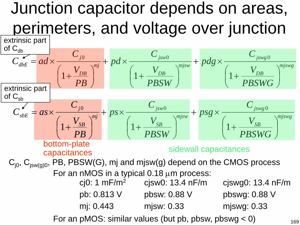
Junction capacitor depends on areas, perimeters, and voltage over junction
mjswgDB
jswgmjsw
DB
jswmj
DB
jdbE
PBSWGV
Cpdg
PBSWV
Cpd
PBV
CadC
+
×+
+
×+
+
×=
111
000
cj0: 1 mF/m2
pb: 0.813 V mj: 0.443
mjswgSB
jswgmjsw
SB
jswmj
SB
jsbE
PBSWGV
Cpsg
PBSWV
Cps
PBV
CasC
+
×+
+
×+
+
×=
111
000
Cj0, Cjsw(g)0, PB, PBSW(G), mj and mjsw(g) depend on the CMOS process For an nMOS in a typical 0.18 µm process:
cjsw0: 13.4 nF/m pbsw: 0.88 V mjsw: 0.33
cjswg0: 13.4 nF/m pbswg: 0.88 V mjswg: 0.33
extrinsic part of Cdb
extrinsic part of Csb
bottom-plate capacitances sidewall capacitances
For an pMOS: similar values (but pb, pbsw, pbswg < 0)

170
Computation of CdbE and CsbE as a function of number of fingers
1 2 4 0
10
20
1 2 4 0
10
20 CsbE
[fF]
CdbE
[fF]
number of fingers
number of fingers S D D S
D
D
source drain D D
D
S
S
S

171
Comparison of parasitic capacitors: Cgs is the largest in moderate/strong inversion
Cgs Cgd Cgb Cdb Csb 0
5
10
15
20
25 C [fF] 4 fingers
Dominance of Cgs is even more pronounced in strong inversion
172
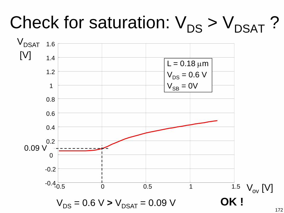
Check for saturation: VDS > VDSAT ?
-0.5 0 0.5 1 1.5 -0.4
-0.2
0
0.2
0.4
0.6
0.8
1
1.2
1.4
1.6
Vov [V]
VDSAT
[V]
0.09 V
VDS = 0.6 V > VDSAT = 0.09 V OK !
L = 0.18 µm VDS = 0.6 V VSB = 0V


