
MOSFET Characteristics at Cryogenic Temperature
Juan M. Avalos Electrical Engineering and Computer Science Department
Christian Brothers University
Memphis, TN USA
Leon Tolbert
Electrical Engineering and Computer Science Department
University of Tennessee
Knoxville, TN USA
Abstract— Efficiency is a large concern in power electronics but
size and weight must be taken into consideration as well. Power
devices in need of thermal sinks for appropriate performance will
affect both size and weight. MOSFET devices are the main
components in the power electronics world because of their
comparatively promising characteristics in power loss and
switching performance. The objective of this research is to obtain
results as to how the MOSFET device will perform in various
temperatures that go as low as liquid nitrogen temperatures.
More than one device was tested and compared in order to get the
best performing. It is believed Cryogenic operation of MOSFET
devices results in improved performance and efficiency. The
switching performance of the devices will be analyzed using the
Double Pulse Test (DPT). Ultimately, the objective of this research
is to design a DC-AC inverter for Boeing & NASA aircraft using
the best performing MOSFET device.
Index Terms—Double Pulse Test, Power Inverter, Cryogenic
Temperature
I. INTRODUCTION
It is essential to understand the structure of MOSFET
devices and the Double Pulse Test process that is used to
analyze them. There are four main characteristics that are being
observed for each device. Each defines the device’s efficiency
and performance. On-state resistance, switching loss, body
diode, and breakdown voltage are the four characteristics that
will be affected by the change in temperature and determine the
device performance gains. Different techniques are used to
obtain each one and will be discussed further on.
The purpose of the Double Pulse Test is to obtain data
reflecting the switching characterization of power devices in a
simplified printed circuit board (PCB). This board allows to
evaluate their switching behaviors as if in an actual power
converter. The Double Pulse Test consists of manually
triggering two pulse as an input to the gate of the device. Each
pulse has its purpose and effect to the device. The length of the
first pulse, in time, builds up a desired current through the
inductor load. The switching transient consists of the turn off
and turn on of the device. The falling edge of the first pulse
corresponds to the turn off transient while the rising edge of the
second pulse corresponds to the turn off.
The components required for this set up are the following:
Device Under Test (DUT)
Inductive Load
Auxiliary DC Power Supply
Waveform Generator
DC bus
Gate drive/driver board
Oscilloscope
Lab procedures for testing devices have to be taken
into consideration for accurate results. Initially, probe
compensation and de-skew correction are necessary for
voltage-current alignment. The yellow scope must compensate
for the input at the gate of the MOSFET while the blue scope
compensates for the drain source voltage. As it is usually
assumed, the channel 1 with yellow waveforms is used as gate-
source voltage measurement, the channel 2 with blue
waveforms is used as drain-source voltage measurement, the
channel 3 with purple waveforms is used as drain-current
measurement, and the channel 4 with green waveforms is used
as load-current measurement. The purple current probe is de-
skewed and the propagation delay for all are minimized as
much as possible. The probes have different purposes such as
the probes being used in channels 1 and 2 for voltage
measurement. The difference in those two channels are the
voltage levels: 1 for ≤ 600V; 2 for 600V ~ 1200V. Different
probes will have different parasitic, which will cause the error
of the measurement, in order to avoid that, the de-skew process
was conducted. Meanwhile, when the 600V-level test was
conducted, same type of probes was used for both channel 1 and
2, the de-skew process was not necessary in this case.
Before any testing is done to the devices, the
circuit board must have exposed, conductive parts covered.
Icing at lower temperatures can cause problems such as shorts
in the circuit leading to damaging equipment. The lowest
temperature, for the chamber, allowed is 93 K (-180°C) and the
highest temperature tested is 23 K (room temperature). Once
the board is ready, it is placed inside the chamber even for room
temperature testing. The room temperature testing is done after
the chamber has been heated up for moisture dissipation. This
procedure mitigates humidity in the inner chamber and reduces
the possibility of short-circuiting due to icing at cryogenic
temperature.
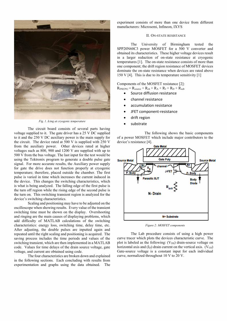
Fig. 1. Icing at cryogenic temperature
The circuit board consists of several parts having
voltage supplied to it. The gate driver has a 25 V DC supplied
to it and the 250 V DC auxiliary power is the main supply for
the circuit. The device rated at 500 V is supplied with 250 V
from the auxiliary power. Other devices rated at higher
voltages such as 800, 900 and 1200 V are supplied with up to
500 V from the bus voltage. The last input for the test would be
using the Tektronix program to generate a double pulse gate
signal. For more accurate results, the Auxiliary power supply
for gate the drive does not function properly at cryogenic
temperature; therefore, placed outside the chamber. The first
pulse is varied in time which increases the current induced in
the device. This changes the switching characteristics, which
is what is being analyzed. The falling edge of the first pulse is
the turn off region while the rising edge of the second pulse is
the turn on. This switching transient region is analyzed for the
device’s switching characteristics.
Scaling and positioning may have to be adjusted on the
oscilloscope when showing results. Every value of the transient
switching time must be shown on the display. Overshooting
and ringing are the main causes of displaying problems, which
add difficulty of MATLAB calculations of the switching
characteristics: energy loss, switching time, delay time, etc.
After adjusting, the double pulses are inputted again and
repeated until the right scaling and positioning is acquired. The
saving process includes the time periods and values of the
switching transient, which are then implemented in a MATLAB
code. Values for time delays of the drain source voltage, gate
voltage, and current are obtained using code.
The four characteristics are broken down and explained
in the following sections. Each concluding with results from
experimentation and graphs using the data obtained. The
experiment consists of more than one device from different
manufacturers: Microsemi, Infineon, IXYS
II. ON-STATE RESISTANCE
The University of Birmingham tested the
SPP20N60C3 power MOSFET for a 500 V converter and
obtained its characteristics. These higher voltage devices result
in a larger reduction of on-state resistance at cryogenic
temperatures [1]. The on-state resistance consists of more than
one component; the drift region resistance of MOSFET devices
dominate the on-state resistance when devices are rated above
150 V [4]. This is due to its temperature sensitivity [1]
Components of the MOSFET resistance [2]:
RDS(ON) = Rsource + Rch + RA + RJ + RD + Rsub
Source diffusion resistance
channel resistance
accumulation resistance
JFET component-resistance
drift region
substrate
The following shows the basic components
of a power MOSFET which include major contributors to the
device’s resistance [4].
Figure 2: MOSFET components
The Lab procedure consists of using a high power
curve tracer which plots the devices characteristic curve. The
plot is labeled as the following: (VDS) drain-source voltage on
horizontal axis and (ID) drain current on the vertical axis. (VGS)
Gate-source voltage is a constant input for each individual
curve, normalized throughout 10 V to 20 V.

Figure 3: On-state Resistance & Body Diode set-up
The resulting curves will allow to find the drain-source
voltage that corresponds to the rated drain current
recommended in the device’s datasheet at various temperatures.
The two values can then be used to calculate the on-state
resistance for each individual device at a certain temperature.
The experiment began at room temperature and decreased to -
180 degrees Celsius in intervals of 50 degrees, resulting in 6
plots for each device.
Figure 4: Curve Tracer Results (VDS vs. ID)
In closing, the RDS-ON significantly reduces as
temperature drops. Due to the improvement of carrier mobility
in the drift region, conduction loss during operation is reduced
[1].
Plot of on-state resistance using curve tracer results:
Figure 5: On-state Resistance Results
III. SWITCHING LOSSES
MOSFET devices have the ability to switch from on
to off in a very small amount of time. Devices differ and behave
differently; therefore, some devices are more efficient than
others in terms of switching.
Load
Inductor
Upper
Diode
Lower
Switch
– +
DC Link
Capacitor
Gate
Driver
DC
source
Signal
Generator
Signal
Isolator/
Logic
AUX
Power
Supply
Scope
Power
Supply
Cryo. Chamber
Figure 6: Set-up for Switching Testing
As earlier stated, the procedure used is called the
double pulse test and allows for the observation of delays and
propagations in the switching transient. The double pulse test
consists of two pulses that are inputted into the gate; the first
falling edge of the first pulse is the turn off transient while the
rising edge of the second pulse is the turn on transient. Before
testing the devices, the probes being used must be well
calibrated and the V-I alignment must be done. Within the
probes being used, the voltage and current probes are ones that
have different characteristic propagation delay and are de-skew
corrected for accuracy enhancement. This process is done for
each individual test.

MOSFET devices have internal parasitic that effect
the behavior in the switching transient. Parasitic inductances
will cause ringing and overshooting; parasitic capacitance
determines a time constant for the circuit and increases delay.
The results in the oscilloscope show the following: VGS, VDS, ID
and inductor current.
The ringing due to parasitics is shown in a turn on transient
response [5]:
Figure 7: DPT Switching Characteristics
These results lead to the calculation of TON_DELAY, TON,
TOFF_DELAY, TOFF, EOFF and EON via MATLAB code. The code
calculates average values over a certain period of time and
value of energy loss. The delay times relate to the amount of
time difference between the current and voltage at an off or on
transient. On and off time corresponds to just the current. It is
the amount of time it takes the current to change within 10% to
90% of its value.
The MOSFET switching performance improves at
lower temperatures, resulting in changes of the calculated
values. The energy loss and the TON for the on period is
significantly reduced while the EOFF and TOFF are only slightly
reduced. The delay times both roughly remained the same
value as temperature decreased. The turning on switching
transient shows the most improvement in the device’s testing at
lower temperatures.
As the device is in the off mode/cut off region, the
reverse drain current is now passing through the body diode
which shorts the source and drain [2]. This creates a high
current path for the device, rather than the drain-source
conducting channel [2]. Reverse recovery characteristics of
the body diode play a significant role in the switching
characteristics of the device. During switching transients, the
reverse recovery is divided into time periods as seen below.
The reverse recovery time is an important factor of losses and
defines the time it takes for drain current to reach a constant
value of zero amperes.
Figure 8: Reverse Recovery behavior
In order to decrease switching and conduction losses,
the input from oscilloscope now includes a dead time. Dead
time is an input that is between two other pulses in which the
inductor current is taking the body diode path.
IV. BREAKDOWN VOLTAGE & BODY DIODE
The power MOSFETs can be operating in three
different stages: cut-off, saturation, and breakdown region. The
breakdown region limits the drain-source voltage amplitude of
the device and is located to the far right of the MOSFET
characteristic curve. The breakdown region varies while it
depends on the gate-source input and temperature. When the
device receives too much voltage across the drain-source
terminals, it reaches the point where the device cannot resist
current and breaks down. This allows a large amount of current
to flow through the device and drastically increases. Due to a
correlation with temperature, on-state resistance shows a non-
linear relationship with the breakdown voltage when plotted.

Figure 9: Breakdown voltage testing schematic
The breakdown voltage configuration allows the
measurement of current when the device is reaching its rated
voltage. Initially, the current is so small it is considered to be
zero and 1 mA when at its breakdown. The devices under
testing had a smaller breakdown voltage then the voltage they
were rated at, when operating at lower temperatures.
Figure 10: Breakdown Voltage Results
The configuration shows the device is set up in series
with a large resistance of 100 kOhms that will limit the current.
While the gate and source are short circuited, voltage is applied
to see how much is needed in order for the ammeter to read
current. The breakdown voltage is set as to when the leakage
current reaches 1 mA.
The diode forward voltage is the amount of voltage
drop across the diode when the source has a specified value of
current. The usual current used is the rated current from the
device’s datasheet.
The following figure shows the configuration when using the
curve tracer for on-state resistance and body diode testing:
Figure 11: Schematic for RDS-ON & Body Diode
V. 77K LIQUID NITROGEN POURING TEST
The lowest temperature used on the devices under
testing was the liquid nitrogen temperature of about 77 K.
Having a minimum temperature operation of about 93 K, the
cooling chamber Delta 9023 model was not functional for the
lowest temperature. Using a Styrofoam container and a larger
plastic container, each device was directly inserted into the
liquid nitrogen while under testing. The previous schematics for
the tests still apply for the 77 K testing; therefore, same
procedures apply.
The time for this is quite limited because the liquid
nitrogen will last about 30 minutes in its liquid state and will
evaporate. This evaporation will cause the temperature to start
to increase again. In order to keep the temperature constant at
around 77 K, liquid nitrogen is constantly being poured in small
amounts into the Styrofoam container. The larger plastic
container is uses as an outer shell in case of leaks or spills.
The image below shows the set up for the lowest temperature
testing:
–+
A
D
G
S
High voltage
DC source
Current limiting resistor
Ampere meter
Device
under
test
(DUT)
Cryo. chamber
450
500
550
600
650
700
750
70 120 170 220 270 320
Bre
ak
do
wn
Vo
lta
ge
(V)
Temperature(K)

VI. CONCLUSION
This research demonstrates a way to reduce the losses
in power MOSFETs. This allows for more efficient power
devices with many advantages when operating at cryogenic
temperature. MOSFET devices have switching characteristics
that will have losses at high frequencies. Under low
temperatures, the devices have slightly faster switching with
less ringing, which is caused by internal parasitic as earlier
stated. On-state resistance drastically decreased due to the
increase of carrier mobilities in the MOSFET’s main resistive
components. These factors allow the efficiency of the device
to increase and enhance its performance at cryogenic
temperatures.
ACKNOWLEDGMENTS
This work was supported primarily by the Engineering
Research Center Program of the National Science Foundation
and the Department of Energy under NSF Award Number
EEC-1041877 and the CURENT Industry Partnership Program.
The help and guidance from Dr. Leon Tolbert and Jingyi Tang,
from the University of Tennessee Knoxville, was greatly
appreciated. All results are remained to be owned and explained
by Boeing Company and NASA supervision.
REFERENCES
[1] C. Jia, “Experimental Investigation of Semiconductor Losses in
Cryogenic DC-DC Converters,” Dept. Elect. Eng., Univ. of
Birmingham, 2008.
[2] V. Barkhordarian. Power MOSFET Basics. [PDF file]. Available:
http://www.infineon.com/dgdl/mosfet.pdf?fileId=5546d4625336
00a4015357444e913f4f
[3] A. Sattar. Power MOSFET Basics. [PDF file]. Available:
http://www.ixys.com/Documents/AppNotes/IXAN0061.pdf
[4] J. Dodge. (2006, March 2). Power MOSFET Tutorial. [PDF file].
Available:http://www.microsemi.com/document-
portal/doc_view/14692-mosfet-tutorial
[5] A. S. J. H. E. S. a. R. P. A. Caiafa, "IGBT operation at cryogenic
temperatures: non-punch-through and punch-through
comparison," in Power Electronics Specialists Conference, 2004.
[6] G. D. H. L. U. L. H. S. J. S. A.E. Schlogl, "Properties of CoolMOS
between 420 K and 80 K-the ideal device for cryogenic
applications," in Power Semiconductor Devices and ICs,
Toronto, Ont., 1999.
[7] A. ,. K.K.Leong, "Power MOSFET operation at cryogenic
temperatures: Comparison between HEXFET®, MDMeshTM
and CoolMOSTM," in International Symposium on Power
Semiconductor Devices & IC's, Hiroshima, 2010.
[8] C. C. D. T. D. P. Thibaut Chailloux, "Characterization and
comparison of 1.2kV SiC power," Materials Science Forum, pp.
814-817, 2015.
[9] T. K. A. R. Y. P. R. L. D. Z. R. W. X. W. Y. J. S. G. K. H. W. P. J.
B. a. A. C. Paul Gemin, "Architecture, Voltage and Components
for a Turboelectric Distributed Propulsion Electric Grid (AVC-
TeDP)," NASA, 2015., 1989


![BSS138PW 60 V, 320 mA N-channel Trench MOSFET · 60 V, 320 mA N-channel Trench MOSFET 6. Thermal characteristics Table 6. Thermal characteristics [1] Device mounted on an FR4 PCB,](https://cdn.vdocument.in/doc/165x107/5b07015b7f8b9ac33f8d9d7b/bss138pw-60-v-320-ma-n-channel-trench-mosfet-v-320-ma-n-channel-trench-mosfet.jpg)
![BSS138BK 60 V, 360 mA N-channel Trench MOSFET V, 360 mA N-channel Trench MOSFET 6. Thermal characteristics Table 6. Thermal characteristics [1] Device mounted on an FR4 PCB, single-sided](https://cdn.vdocument.in/doc/165x107/5b0719bc7f8b9ae9628df8b1/bss138bk-60-v-360-ma-n-channel-trench-mosfet-v-360-ma-n-channel-trench-mosfet.jpg)
