
MRI4 – ModbusHighPROTEC
Data point list
Manual DOK-TD-MRI4MDE

Table of Contents
Table of ContentsTABLE OF CONTENTS................................................................................................................................................................................................................... 2MODBUS PARAMETERS................................................................................................................................................................................................................. 3
Notes for the SCADA-System....................................................................................................................................................................................................................... 4SPECIFIC MODBUS FUNCTION CODES.............................................................................................................................................................................................. 5
Setting Date and Time................................................................................................................................................................................................................................. 10Supported MODBUS- Error Messages........................................................................................................................................................................................................ 11
APPENDIX - DATA POINT LISTS.................................................................................................................................................................................................... 12Signals........................................................................................................................................................................................................................................................ 12Measuring values........................................................................................................................................................................................................................................ 81Commands................................................................................................................................................................................................................................................. 96Settings..................................................................................................................................................................................................................................................... 101Cause of trip.............................................................................................................................................................................................................................................. 103
md5_1md5_2RMS_Handoff: 35616Datei: ?This Manual is valid for version (applies for Modbus RTU and Modbus TCP):
Version 3.4.a
Build: 35596
Page 2 EN MRI4 Modbus 09/17

Modbus Parameters
Modbus ParametersFor the Modbus Protocol several parameters have to be set which are relevant for the communication between the control system (SCADA) and the device. The parameters and their setting possibilities or value ranges are shown in the table below.
ATTENTION!The Parameters are described within the appendix of the device manual (chapter Modbus).
EN MRI4 Modbus 09/17 Page 3

Modbus Parameters
Notes for the SCADA-SystemWhen using Modbus RTU the following times have to be considered by the control system and are fixed within the device :The dwell times (tD ) before start of a telegram must at least be set to 3.5 characters.
Examples:
3.5 characters 9600 Baud = 4 ms3.5 characters 19200 Baud = 2 ms3.6 3.5 characters 38400 Baud = 1 ms
Start of a new telegram is expected when the dwell time (tD ) is > 3.5 characters.
The fact that the probability of disruptions during transmission of a telegram increases with its length has to be taken into duly consideration and thus a query to the Slave should be possibly such that the response telegram is not much longer than 32 Byte.
Page 4 EN MRI4 Modbus 09/17

Specific Modbus Function Codes
Specific Modbus Function CodesFor reading out data from the device or to carry out commands, the services listed in the table, also called »Function Codes«, are supported.
Function-code
Designation Description
3 Read Holding Registers There are single or several data words read as from a specific data word address. Only status addresses and parameter addresses can be read.
4 Read Input Registers There are single or several data words read as from a specific data word address. Only measuring values can be read.5 Write single Output (Bit) All other values are illegal and will not affect the output. Via this function code acknowledgments can be executed as well
as counters reseted or blockings set.8 Loopback Test Test function for the communication system16 Load Multiple Registers There are single or several data words written as from a specific data word address. Table 3.1: function codes
EN MRI4 Modbus 09/17 Page 5

Specific Modbus Function Codes
On the following pages the Modbus functions are described in detail:
Function-Code 3/4:
QuerySlaveaddress
3/4 Register addressHI
Register addressLO
Register numberHI
Register numberLO
Check-sumHI
Check-sumLO
ResponseSlaveaddress
3/4 Bytenumber
Register 0HI
Register 0LO
... Check-sumHI
Check-sumLO
Register address (HI*256 + LO)The data word address from where reading should start.
Register number (HI*256 + LO)Number of data words to be read. Valid range: 1..125
Byte numberNumber of subsequent Bytes containing data words.
RegisterData words read out of the device (Highbyte and Lowbyte).
Page 6 EN MRI4 Modbus 09/17

Specific Modbus Function Codes
Float Values IEEE 754
For displaying a float value, it is important to save received bytes in a correct order. A float value in Modbus will be transmitted in “Big Endian“ format (Motorola Format), that means most significant byte is transmitted first.For saving received bytes in Modbus master it must be considered which architecture is used. Is Modbus Master is a “Little Endian” architecture, received frame needs to be swapped to corresponding memory addresses. If it is not saved in correct order it is possible that displayed value is useless.
EN MRI4 Modbus 09/17 Page 7

Specific Modbus Function Codes
Function Code 5:
QuerySlaveaddress
5 Register addressHI
Register addressLO
Register dataHI
Register dataLO
Check-sumHI
Check-sumLO
ResponseSlaveaddress
5 Register addressHI
Register addressLO
Register dataHI
Register dataLO
Check-sumHI
Check-sumLO
Register address (HI*256 + LO)Data word address to be written
Register dataValue of the data word to be written (Highbyte and Lowbyte).
Permitted value range : FF00 hex request for a single bit to be on: This often means to reset a counter, execute acknowledgments or set blockings signals.0000 hex request for a single bit to be off: This often means to deactivate blocking signals or to reset single bits.
Function Code 8:
QuerySlaveaddress
8 Data DiagCode HI0x00
Data DiagCode LO0x00
Test data Test data Check-sumHI
Check-sumLO
ResponseSlaveaddress
8 Data DiagCode HI
Data DiagCode LO
Test data Test data Check-sumHI
Check-sumLO
Data Diag Code HI (high), Data Diag Code LO ( Low)Diagnostic Code (subfunction code of function code 8) for testing the communication system. The Diagnostic Code „Return Query Data“ (0x00, 0x00) is being supported.
Test DataBy using the Diagnostic Code 0x00 0x00, the transmitted data is sent back to the Master unchanged.
Page 8 EN MRI4 Modbus 09/17

Specific Modbus Function Codes
Function Code 16:
QuerySlaveaddress
16 Register addressHI
Register addressLO
Register numberHI
Register numberLO
Byte number Register 0HI
Register 0LO
... Check-sumHI
Check-sumLO
ResponseSlaveaddress
16 Register addressHI
Register addressLO
Register numberHI
Register numberLO
Check-sumHI
Check-sumLO
Register address (HI*256 + LO)Data word address as from where writing should start.
Register number (HI*256 + LO)Query: Number of data words to be written. Valid range: 1..123Response: Number of data words written.
Byte numberNumber of subsequent Bytes to contain data words.
RegisterData words read out of the device (Highbyte und Lowbyte).
EN MRI4 Modbus 09/17 Page 9

Specific Modbus Function Codes
Setting Date and TimeDate and time can be set by means of function code 16 and read with function code 3. If the device address 0 (broadcast address) is selected, the times of all devices connected to this bus are simultaneously reset. The devices do not respond to a broadcast command.
Page 10 EN MRI4 Modbus 09/17

Specific Modbus Function Codes
Supported MODBUS- Error MessagesException Response Telegrams are described within the general “Modbus Application Protocol Specification". An exception response table with examples is shown there. The table below contains just the actually used codes. In case the device has recognized an error it will react in the following way:
Exception Code
Designation Description
1 Illegal Function The message received includes a function code which is not supported by the Slave.2 Illegal Data Address Access was sought on a data word address not included in the data module. 3 Illegal Data Value The received message contains an invalid data structure (e.g. wrong number of data bytes).4 Slave Device Failure An unrecoverable error occurred while the server (or slave) was attempting to perform the requested action.
The response given by the device in a failure case has the following format:
Slave Address
0x80+ Function Code
Exception Code
Check- sum HI
Check-sum LO
In the second Byte of the response the Function Code is sent with the highest Bit set to 1. This is equivalent to an addition by 0x80. The third Byte holds the Exception Code of the error message.
EN MRI4 Modbus 09/17 Page 11

Appendix - Data Point Lists
Appendix - Data Point Lists
Signals
Module
( - ANSI / IEEE Device Number )
Subgroup
Names
Functions
Start Register Address
No. of Modbus Registers
Function Code Format Bit Mask
/ (Bit Position)
Unit Description
AR - 79 46 1 3 Structactive 46 1 3 Bit 0x1
(1)
- Signal: active
ExBlo 46 1 3 Bit 0x2
(2)
- Signal: External Blocking
running 46 1 3 Bit 0x8
(4)
- Signal: Auto Reclosing running
t-dead 46 1 3 Bit 0x10
(5)
- Signal: Dead time between trip and reclosure attempt
successful (*) 46 1 3 Bit 0x100
(9)
- Signal: Auto Reclosing successful
failed (*) 46 1 3 Bit 0x200
(10)
- Signal: Auto Reclosing failure
t-AR Supervision
46 1 3 Bit 0x1000
(13)
- Signal: AR Supervision
AR - 79 47 1 3 StructExBlo1-I 47 1 3 Bit 0x1
(1)
- Module input state: External blocking1
Page 12 EN MRI4 Modbus 09/17

Appendix - Data Point Lists
Module
( - ANSI / IEEE Device Number )
Subgroup
Names
Functions
Start Register Address
No. of Modbus Registers
Function Code Format Bit Mask
/ (Bit Position)
Unit Description
ExBlo2-I 47 1 3 Bit 0x2
(2)
- Module input state: External blocking2
CB ON Cmd 47 1 3 Bit 0x10
(5)
- Signal: CB switch ON Command
Pre Shot (*) 47 1 3 Bit 0x20
(6)
- Pre Shot Control
Shot 1 (*) 47 1 3 Bit 0x40
(7)
- Shot Control
Shot 2 (*) 47 1 3 Bit 0x80
(8)
- Shot Control
Shot 3 (*) 47 1 3 Bit 0x100
(9)
- Shot Control
Shot 4 (*) 47 1 3 Bit 0x200
(10)
- Shot Control
Shot 5 (*) 47 1 3 Bit 0x400
(11)
- Shot Control
Shot 6 (*) 47 1 3 Bit 0x800
(12)
- Shot Control
AR - 79 156 1 3 StructEx Lock-I 156 1 3 Bit 0x1
(1)
- Module input state: External AR lockout.
EN MRI4 Modbus 09/17 Page 13
Appendix - Data Point Lists
Module
( - ANSI / IEEE Device Number )
Subgroup
Names
Functions
Start Register Address
No. of Modbus Registers
Function Code Format Bit Mask
/ (Bit Position)
Unit Description
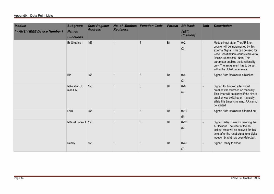
Ex Shot Inc-I 156 1 3 Bit 0x2
(2)
- Module input state: The AR Shot counter will be incremented by this external Signal. This can be used for Zone Coordination (of upstream Auto Reclosure devices). Note: This parameter enables the functionality only. The assignment has to be set within the global parameters.
Blo 156 1 3 Bit 0x4
(3)
- Signal: Auto Reclosure is blocked
t-Blo after CB man ON
156 1 3 Bit 0x8
(4)
- Signal: AR blocked after circuit breaker was switched on manually. This timer will be started if the circuit breaker was switched on manually. While this timer is running, AR cannot be started.
Lock 156 1 3 Bit 0x10
(5)
- Signal: Auto Reclosure is locked out
t-Reset Lockout 156 1 3 Bit 0x20
(6)
- Signal: Delay Timer for resetting the AR lockout. The reset of the AR lockout state will be delayed for this time, after the reset signal (e.g digital input or Scada) has been detected .
Ready 156 1 3 Bit 0x40
(7)
- Signal: Ready to shoot
Page 14 EN MRI4 Modbus 09/17

Appendix - Data Point Lists
Module
( - ANSI / IEEE Device Number )
Subgroup
Names
Functions
Start Register Address
No. of Modbus Registers
Function Code Format Bit Mask
/ (Bit Position)
Unit Description
t-Run2Ready 156 1 3 Bit 0x80
(8)
- Signal: Examination Time: If the Circuit Breaker remains after a reclosure attempt for the duration of this timer in the Closed position, the AR has been successful and the AR module returns into the ready state.
Standby 156 1 3 Bit 0x100
(9)
- Signal: Standby
Service Alarm 1
156 1 3 Bit 0x200
(10)
- Signal: AR - Service Alarm 1, too many switching operations
Service Alarm 2
156 1 3 Bit 0x400
(11)
- Signal: AR - Service Alarm 2 - too many switching operations
Max Shots / h exceeded
156 1 3 Bit 0x800
(12)
- Signal: The maximum allowed number of shots per hour has been exceeded.
BO Slot X2 1003 1 3 StructBO 1 1003 1 3 Bit 0x1
(1)
- Signal: Binary Output Relay
BO 2 1003 1 3 Bit 0x2
(2)
- Signal: Binary Output Relay
BO 3 1003 1 3 Bit 0x4
(3)
- Signal: Binary Output Relay
BO 4 1003 1 3 Bit 0x8
(4)
- Signal: Binary Output Relay
EN MRI4 Modbus 09/17 Page 15

Appendix - Data Point Lists
Module
( - ANSI / IEEE Device Number )
Subgroup
Names
Functions
Start Register Address
No. of Modbus Registers
Function Code Format Bit Mask
/ (Bit Position)
Unit Description
BO 5 1003 1 3 Bit 0x10
(5)
- Signal: Binary Output Relay
DISARMED! 1003 1 3 Bit 0x40
(7)
- Signal: CAUTION! RELAYS DISARMED in order to safely perform maintenance while eliminating the risk of taking an entire process off-line. (Note: The Self Supervision Contact cannot be disarmed). YOU MUST ENSURE that the relays are ARMED AGAIN after maintenance
Outs forced 1003 1 3 Bit 0x80
(8)
- Signal: The State of at least one Relay Output has been set by force. That means that the state of at least one Relay is forced and hence does not show the state of the assigned signals.
CBF - 50BF, 62BF 53 1 3 StructExBlo1-I 53 1 3 Bit 0x1
(1)
- Module input state: External blocking1
ExBlo2-I 53 1 3 Bit 0x2
(2)
- Module input state: External blocking2
active 53 1 3 Bit 0x4
(3)
- Signal: active
ExBlo 53 1 3 Bit 0x8
(4)
- Signal: External Blocking
Trigger1-I 53 1 3 Bit 0x10
(5)
- Module Input: Trigger that will start the CBF
Page 16 EN MRI4 Modbus 09/17

Appendix - Data Point Lists
Module
( - ANSI / IEEE Device Number )
Subgroup
Names
Functions
Start Register Address
No. of Modbus Registers
Function Code Format Bit Mask
/ (Bit Position)
Unit Description
Trigger2-I 53 1 3 Bit 0x20
(6)
- Module Input: Trigger that will start the CBF
Trigger3-I 53 1 3 Bit 0x40
(7)
- Module Input: Trigger that will start the CBF
running 53 1 3 Bit 0x80
(8)
- Signal: CBF-Module started
Alarm (*) 53 1 3 Bit 0x100
(9)
- Signal: Circuit Breaker Failure
Lockout (*) 53 1 3 Bit 0x200
(10)
- Signal: Lockout
Waiting for Trigger (*)
53 1 3 Bit 0x400
(11)
- Waiting for Trigger
CLPU 66 1 3 StructExBlo1-I 66 1 3 Bit 0x1
(1)
- Module input state: External blocking
ExBlo2-I 66 1 3 Bit 0x2
(2)
- Module input state: External blocking
Ex rev Interl-I 66 1 3 Bit 0x4
(3)
- Module input state: External reverse interlocking
active 66 1 3 Bit 0x8
(4)
- Signal: active
ExBlo 66 1 3 Bit 0x10
(5)
- Signal: External Blocking
EN MRI4 Modbus 09/17 Page 17

Appendix - Data Point Lists
Module
( - ANSI / IEEE Device Number )
Subgroup
Names
Functions
Start Register Address
No. of Modbus Registers
Function Code Format Bit Mask
/ (Bit Position)
Unit Description
Ex rev Interl 66 1 3 Bit 0x20
(6)
- Signal: External reverse Interlocking
enabled 66 1 3 Bit 0x200
(10)
- Signal: Cold Load enabled
detected (*) 66 1 3 Bit 0x400
(11)
- Signal: Cold Load detected
I< 66 1 3 Bit 0x800
(12)
- Signal: No Load Current.
AR Blo 66 1 3 Bit 0x1000
(13)
- Signal: Blocked by AR
Load Inrush 66 1 3 Bit 0x2000
(14)
- Signal: Load Inrush
Settle Time 66 1 3 Bit 0x4000
(15)
- Signal: Settle Time
CTS - 60L 137 1 3 StructExBlo1-I 137 1 3 Bit 0x1
(1)
- Module input state: External blocking1
ExBlo2-I 137 1 3 Bit 0x2
(2)
- Module input state: External blocking2
active 137 1 3 Bit 0x4
(3)
- Signal: active
ExBlo 137 1 3 Bit 0x8
(4)
- Signal: External Blocking
Page 18 EN MRI4 Modbus 09/17

Appendix - Data Point Lists
Module
( - ANSI / IEEE Device Number )
Subgroup
Names
Functions
Start Register Address
No. of Modbus Registers
Function Code Format Bit Mask
/ (Bit Position)
Unit Description
Alarm 137 1 3 Bit 0x10
(5)
- Signal: Alarm Current Transformer Measuring Circuit Supervision
Ctrl 176 1 3 StructLocal 176 1 3 Bit 0x1
(1)
- Switching Authority: Local
Remote 176 1 3 Bit 0x2
(2)
- Switching Authority: Remote
NonInterl 176 1 3 Bit 0x4
(3)
- Non-Interlocking is active
SG Disturb 176 1 3 Bit 0x8
(4)
- Minimum one Switchgear is disturbed.
SG Indeterm 176 1 3 Bit 0x10
(5)
- Minimum one Switchgear is moving (Position cannot be determined).
DI Slot X1 1000 1 3 StructDI 1 1000 1 3 Bit 0x1
(1)
- Signal: Digital Input
DI 2 1000 1 3 Bit 0x2
(2)
- Signal: Digital Input
DI 3 1000 1 3 Bit 0x4
(3)
- Signal: Digital Input
DI 4 1000 1 3 Bit 0x8
(4)
- Signal: Digital Input
EN MRI4 Modbus 09/17 Page 19

Appendix - Data Point Lists
Module
( - ANSI / IEEE Device Number )
Subgroup
Names
Functions
Start Register Address
No. of Modbus Registers
Function Code Format Bit Mask
/ (Bit Position)
Unit Description
DI 5 1000 1 3 Bit 0x10
(5)
- Signal: Digital Input
DI 6 1000 1 3 Bit 0x20
(6)
- Signal: Digital Input
DI 7 1000 1 3 Bit 0x40
(7)
- Signal: Digital Input
DI 8 1000 1 3 Bit 0x80
(8)
- Signal: Digital Input
ExP[1] 49 1 3 StructExBlo1-I 49 1 3 Bit 0x1
(1)
- Module input state: External blocking1
ExBlo2-I 49 1 3 Bit 0x2
(2)
- Module input state: External blocking2
ExBlo TripCmd-I
49 1 3 Bit 0x4
(3)
- Module input state: External Blocking of the Trip Command
Alarm-I 49 1 3 Bit 0x8
(4)
- Module input state: Alarm
Trip-I 49 1 3 Bit 0x10
(5)
- Module input state: Trip
active 49 1 3 Bit 0x20
(6)
- Signal: active
ExBlo 49 1 3 Bit 0x40
(7)
- Signal: External Blocking
Page 20 EN MRI4 Modbus 09/17

Appendix - Data Point Lists
Module
( - ANSI / IEEE Device Number )
Subgroup
Names
Functions
Start Register Address
No. of Modbus Registers
Function Code Format Bit Mask
/ (Bit Position)
Unit Description
Blo TripCmd 49 1 3 Bit 0x80
(8)
- Signal: Trip Command blocked
ExBlo TripCmd 49 1 3 Bit 0x100
(9)
- Signal: External Blocking of the Trip Command
Alarm 49 1 3 Bit 0x200
(10)
- Signal: Alarm
Trip (*) 49 1 3 Bit 0x400
(11)
- Signal: Trip
TripCmd (*) 49 1 3 Bit 0x800
(12)
- Signal: Trip Command
ExP[2] 50 1 3 StructExBlo1-I 50 1 3 Bit 0x1
(1)
- Module input state: External blocking1
ExBlo2-I 50 1 3 Bit 0x2
(2)
- Module input state: External blocking2
ExBlo TripCmd-I
50 1 3 Bit 0x4
(3)
- Module input state: External Blocking of the Trip Command
Alarm-I 50 1 3 Bit 0x8
(4)
- Module input state: Alarm
Trip-I 50 1 3 Bit 0x10
(5)
- Module input state: Trip
active 50 1 3 Bit 0x20
(6)
- Signal: active
EN MRI4 Modbus 09/17 Page 21

Appendix - Data Point Lists
Module
( - ANSI / IEEE Device Number )
Subgroup
Names
Functions
Start Register Address
No. of Modbus Registers
Function Code Format Bit Mask
/ (Bit Position)
Unit Description
ExBlo 50 1 3 Bit 0x40
(7)
- Signal: External Blocking
Blo TripCmd 50 1 3 Bit 0x80
(8)
- Signal: Trip Command blocked
ExBlo TripCmd 50 1 3 Bit 0x100
(9)
- Signal: External Blocking of the Trip Command
Alarm 50 1 3 Bit 0x200
(10)
- Signal: Alarm
Trip (*) 50 1 3 Bit 0x400
(11)
- Signal: Trip
TripCmd (*) 50 1 3 Bit 0x800
(12)
- Signal: Trip Command
ExP[3] 51 1 3 StructExBlo1-I 51 1 3 Bit 0x1
(1)
- Module input state: External blocking1
ExBlo2-I 51 1 3 Bit 0x2
(2)
- Module input state: External blocking2
ExBlo TripCmd-I
51 1 3 Bit 0x4
(3)
- Module input state: External Blocking of the Trip Command
Alarm-I 51 1 3 Bit 0x8
(4)
- Module input state: Alarm
Trip-I 51 1 3 Bit 0x10
(5)
- Module input state: Trip
Page 22 EN MRI4 Modbus 09/17

Appendix - Data Point Lists
Module
( - ANSI / IEEE Device Number )
Subgroup
Names
Functions
Start Register Address
No. of Modbus Registers
Function Code Format Bit Mask
/ (Bit Position)
Unit Description
active 51 1 3 Bit 0x20
(6)
- Signal: active
ExBlo 51 1 3 Bit 0x40
(7)
- Signal: External Blocking
Blo TripCmd 51 1 3 Bit 0x80
(8)
- Signal: Trip Command blocked
ExBlo TripCmd 51 1 3 Bit 0x100
(9)
- Signal: External Blocking of the Trip Command
Alarm 51 1 3 Bit 0x200
(10)
- Signal: Alarm
Trip (*) 51 1 3 Bit 0x400
(11)
- Signal: Trip
TripCmd (*) 51 1 3 Bit 0x800
(12)
- Signal: Trip Command
ExP[4] 52 1 3 StructExBlo1-I 52 1 3 Bit 0x1
(1)
- Module input state: External blocking1
ExBlo2-I 52 1 3 Bit 0x2
(2)
- Module input state: External blocking2
ExBlo TripCmd-I
52 1 3 Bit 0x4
(3)
- Module input state: External Blocking of the Trip Command
Alarm-I 52 1 3 Bit 0x8
(4)
- Module input state: Alarm
EN MRI4 Modbus 09/17 Page 23

Appendix - Data Point Lists
Module
( - ANSI / IEEE Device Number )
Subgroup
Names
Functions
Start Register Address
No. of Modbus Registers
Function Code Format Bit Mask
/ (Bit Position)
Unit Description
Trip-I 52 1 3 Bit 0x10
(5)
- Module input state: Trip
active 52 1 3 Bit 0x20
(6)
- Signal: active
ExBlo 52 1 3 Bit 0x40
(7)
- Signal: External Blocking
Blo TripCmd 52 1 3 Bit 0x80
(8)
- Signal: Trip Command blocked
ExBlo TripCmd 52 1 3 Bit 0x100
(9)
- Signal: External Blocking of the Trip Command
Alarm 52 1 3 Bit 0x200
(10)
- Signal: Alarm
Trip (*) 52 1 3 Bit 0x400
(11)
- Signal: Trip
TripCmd (*) 52 1 3 Bit 0x800
(12)
- Signal: Trip Command
Fast Status Register 5000 1 3 Struct
Page 24 EN MRI4 Modbus 09/17

Appendix - Data Point Lists
Module
( - ANSI / IEEE Device Number )
Subgroup
Names
Functions
Start Register Address
No. of Modbus Registers
Function Code Format Bit Mask
/ (Bit Position)
Unit Description
Device Type 5000 1 3 Bit 0xffff
(1)
- Device Type: Device type code for relationship between device name and its Modbus code.
Woodward:
MRI4 - 1000
MRU4 - 1001
MRA4 - 1002
MCA4 - 1003
MRDT4 - 1005
MCDTV4 - 1006
MCDGV4 - 1007
MRM4 - 1009
MRMV4 - 1010
MCDLV4 - 1011Fast Status Register 5001 1 3 Struct
Comm Version 5001 1 3 Bit 0xffff
(1)
- Modbus Communication version. This version number changes if something becomes incompatible between different Modbus releases.
Fast Status Register 5002 1 3 StructConfig Bin Inp1-I
5002 1 3 Bit 0x1
(1)
- State of the module input: Config Bin Inp
EN MRI4 Modbus 09/17 Page 25

Appendix - Data Point Lists
Module
( - ANSI / IEEE Device Number )
Subgroup
Names
Functions
Start Register Address
No. of Modbus Registers
Function Code Format Bit Mask
/ (Bit Position)
Unit Description
Config Bin Inp2-I
5002 1 3 Bit 0x2
(2)
- State of the module input: Config Bin Inp
Config Bin Inp3-I
5002 1 3 Bit 0x4
(3)
- State of the module input: Config Bin Inp
Config Bin Inp4-I
5002 1 3 Bit 0x8
(4)
- State of the module input: Config Bin Inp
Config Bin Inp5-I
5002 1 3 Bit 0x10
(5)
- State of the module input: Config Bin Inp
Config Bin Inp6-I
5002 1 3 Bit 0x20
(6)
- State of the module input: Config Bin Inp
Config Bin Inp7-I
5002 1 3 Bit 0x40
(7)
- State of the module input: Config Bin Inp
Config Bin Inp8-I
5002 1 3 Bit 0x80
(8)
- State of the module input: Config Bin Inp
Config Bin Inp9-I
5002 1 3 Bit 0x100
(9)
- State of the module input: Config Bin Inp
Config Bin Inp10-I
5002 1 3 Bit 0x200
(10)
- State of the module input: Config Bin Inp
Config Bin Inp11-I
5002 1 3 Bit 0x400
(11)
- State of the module input: Config Bin Inp
Config Bin Inp12-I
5002 1 3 Bit 0x800
(12)
- State of the module input: Config Bin Inp
Page 26 EN MRI4 Modbus 09/17

Appendix - Data Point Lists
Module
( - ANSI / IEEE Device Number )
Subgroup
Names
Functions
Start Register Address
No. of Modbus Registers
Function Code Format Bit Mask
/ (Bit Position)
Unit Description
Config Bin Inp13-I
5002 1 3 Bit 0x1000
(13)
- State of the module input: Config Bin Inp
Config Bin Inp14-I
5002 1 3 Bit 0x2000
(14)
- State of the module input: Config Bin Inp
Config Bin Inp15-I
5002 1 3 Bit 0x4000
(15)
- State of the module input: Config Bin Inp
Config Bin Inp16-I
5002 1 3 Bit 0x8000
(16)
- State of the module input: Config Bin Inp
Fast Status Register 5003 1 3 StructConfig Bin Inp17-I
5003 1 3 Bit 0x1
(1)
- State of the module input: Config Bin Inp
Config Bin Inp18-I
5003 1 3 Bit 0x2
(2)
- State of the module input: Config Bin Inp
Config Bin Inp19-I
5003 1 3 Bit 0x4
(3)
- State of the module input: Config Bin Inp
Config Bin Inp20-I
5003 1 3 Bit 0x8
(4)
- State of the module input: Config Bin Inp
Config Bin Inp21-I
5003 1 3 Bit 0x10
(5)
- State of the module input: Config Bin Inp
Config Bin Inp22-I
5003 1 3 Bit 0x20
(6)
- State of the module input: Config Bin Inp
Config Bin Inp23-I
5003 1 3 Bit 0x40
(7)
- State of the module input: Config Bin Inp
EN MRI4 Modbus 09/17 Page 27

Appendix - Data Point Lists
Module
( - ANSI / IEEE Device Number )
Subgroup
Names
Functions
Start Register Address
No. of Modbus Registers
Function Code Format Bit Mask
/ (Bit Position)
Unit Description
Config Bin Inp24-I
5003 1 3 Bit 0x80
(8)
- State of the module input: Config Bin Inp
Config Bin Inp25-I
5003 1 3 Bit 0x100
(9)
- State of the module input: Config Bin Inp
Config Bin Inp26-I
5003 1 3 Bit 0x200
(10)
- State of the module input: Config Bin Inp
Config Bin Inp27-I
5003 1 3 Bit 0x400
(11)
- State of the module input: Config Bin Inp
Config Bin Inp28-I
5003 1 3 Bit 0x800
(12)
- State of the module input: Config Bin Inp
Config Bin Inp29-I
5003 1 3 Bit 0x1000
(13)
- State of the module input: Config Bin Inp
Config Bin Inp30-I
5003 1 3 Bit 0x2000
(14)
- State of the module input: Config Bin Inp
Config Bin Inp31-I
5003 1 3 Bit 0x4000
(15)
- State of the module input: Config Bin Inp
Config Bin Inp32-I
5003 1 3 Bit 0x8000
(16)
- State of the module input: Config Bin Inp
Fast Status Register 5004 1 3 Struct
Page 28 EN MRI4 Modbus 09/17

Appendix - Data Point Lists
Module
( - ANSI / IEEE Device Number )
Subgroup
Names
Functions
Start Register Address
No. of Modbus Registers
Function Code Format Bit Mask
/ (Bit Position)
Unit Description
Trip (*) 5004 1 3 Bit 0xffff
(1)
- Initial reason of trip. It is transferred as an integer value in the MODBUS register 5004 and essentially corresponds to the “Trip” entry in the fault record, i. e. to the name of the protective module that tripped first. Look up the definition of these integer values (i. e. the mapping trip code number-->module name) in the “Cause of Trip” table within the SCADA documentation.
I2>[1] - 46 82 1 3 StructExBlo1-I 82 1 3 Bit 0x1
(1)
- Module input state: External blocking1
ExBlo2-I 82 1 3 Bit 0x2
(2)
- Module input state: External blocking2
ExBlo TripCmd-I
82 1 3 Bit 0x4
(3)
- Module input state: External Blocking of the Trip Command
active 82 1 3 Bit 0x8
(4)
- Signal: active
ExBlo 82 1 3 Bit 0x10
(5)
- Signal: External Blocking
Blo TripCmd 82 1 3 Bit 0x20
(6)
- Signal: Trip Command blocked
ExBlo TripCmd 82 1 3 Bit 0x40
(7)
- Signal: External Blocking of the Trip Command
EN MRI4 Modbus 09/17 Page 29

Appendix - Data Point Lists
Module
( - ANSI / IEEE Device Number )
Subgroup
Names
Functions
Start Register Address
No. of Modbus Registers
Function Code Format Bit Mask
/ (Bit Position)
Unit Description
Alarm 82 1 3 Bit 0x80
(8)
- Signal: Alarm Negative Sequence
Trip (*) 82 1 3 Bit 0x100
(9)
- Signal: Trip
TripCmd (*) 82 1 3 Bit 0x200
(10)
- Signal: Trip Command
I2>[2] - 46 83 1 3 StructExBlo1-I 83 1 3 Bit 0x1
(1)
- Module input state: External blocking1
ExBlo2-I 83 1 3 Bit 0x2
(2)
- Module input state: External blocking2
ExBlo TripCmd-I
83 1 3 Bit 0x4
(3)
- Module input state: External Blocking of the Trip Command
active 83 1 3 Bit 0x8
(4)
- Signal: active
ExBlo 83 1 3 Bit 0x10
(5)
- Signal: External Blocking
Blo TripCmd 83 1 3 Bit 0x20
(6)
- Signal: Trip Command blocked
ExBlo TripCmd 83 1 3 Bit 0x40
(7)
- Signal: External Blocking of the Trip Command
Alarm 83 1 3 Bit 0x80
(8)
- Signal: Alarm Negative Sequence
Page 30 EN MRI4 Modbus 09/17

Appendix - Data Point Lists
Module
( - ANSI / IEEE Device Number )
Subgroup
Names
Functions
Start Register Address
No. of Modbus Registers
Function Code Format Bit Mask
/ (Bit Position)
Unit Description
Trip (*) 83 1 3 Bit 0x100
(9)
- Signal: Trip
TripCmd (*) 83 1 3 Bit 0x200
(10)
- Signal: Trip Command
IG[1] - 50N, 51N 15 1 3 StructExBlo1-I 15 1 3 Bit 0x1
(1)
- Module input state: External blocking1
ExBlo2-I 15 1 3 Bit 0x2
(2)
- Module input state: External blocking2
ExBlo TripCmd-I
15 1 3 Bit 0x4
(3)
- Module input state: External Blocking of the Trip Command
Ex rev Interl-I 15 1 3 Bit 0x8
(4)
- Module input state: External reverse interlocking
active 15 1 3 Bit 0x10
(5)
- Signal: active
ExBlo 15 1 3 Bit 0x20
(6)
- Signal: External Blocking
Ex rev Interl 15 1 3 Bit 0x40
(7)
- Signal: External reverse Interlocking
Blo TripCmd 15 1 3 Bit 0x80
(8)
- Signal: Trip Command blocked
ExBlo TripCmd 15 1 3 Bit 0x100
(9)
- Signal: External Blocking of the Trip Command
EN MRI4 Modbus 09/17 Page 31

Appendix - Data Point Lists
Module
( - ANSI / IEEE Device Number )
Subgroup
Names
Functions
Start Register Address
No. of Modbus Registers
Function Code Format Bit Mask
/ (Bit Position)
Unit Description
IGH2 Blo 15 1 3 Bit 0x200
(10)
- Signal: blocked by an inrush
Alarm 15 1 3 Bit 0x400
(11)
- Signal: Alarm IG
Trip (*) 15 1 3 Bit 0x800
(12)
- Signal: Trip
TripCmd (*) 15 1 3 Bit 0x1000
(13)
- Signal: Trip Command
IG[2] - 50N, 51N 16 1 3 StructExBlo1-I 16 1 3 Bit 0x1
(1)
- Module input state: External blocking1
ExBlo2-I 16 1 3 Bit 0x2
(2)
- Module input state: External blocking2
ExBlo TripCmd-I
16 1 3 Bit 0x4
(3)
- Module input state: External Blocking of the Trip Command
Ex rev Interl-I 16 1 3 Bit 0x8
(4)
- Module input state: External reverse interlocking
active 16 1 3 Bit 0x10
(5)
- Signal: active
ExBlo 16 1 3 Bit 0x20
(6)
- Signal: External Blocking
Ex rev Interl 16 1 3 Bit 0x40
(7)
- Signal: External reverse Interlocking
Page 32 EN MRI4 Modbus 09/17

Appendix - Data Point Lists
Module
( - ANSI / IEEE Device Number )
Subgroup
Names
Functions
Start Register Address
No. of Modbus Registers
Function Code Format Bit Mask
/ (Bit Position)
Unit Description
Blo TripCmd 16 1 3 Bit 0x80
(8)
- Signal: Trip Command blocked
ExBlo TripCmd 16 1 3 Bit 0x100
(9)
- Signal: External Blocking of the Trip Command
IGH2 Blo 16 1 3 Bit 0x200
(10)
- Signal: blocked by an inrush
Alarm 16 1 3 Bit 0x400
(11)
- Signal: Alarm IG
Trip (*) 16 1 3 Bit 0x800
(12)
- Signal: Trip
TripCmd (*) 16 1 3 Bit 0x1000
(13)
- Signal: Trip Command
IG[3] - 50N, 51N 17 1 3 StructExBlo1-I 17 1 3 Bit 0x1
(1)
- Module input state: External blocking1
ExBlo2-I 17 1 3 Bit 0x2
(2)
- Module input state: External blocking2
ExBlo TripCmd-I
17 1 3 Bit 0x4
(3)
- Module input state: External Blocking of the Trip Command
Ex rev Interl-I 17 1 3 Bit 0x8
(4)
- Module input state: External reverse interlocking
active 17 1 3 Bit 0x10
(5)
- Signal: active
EN MRI4 Modbus 09/17 Page 33

Appendix - Data Point Lists
Module
( - ANSI / IEEE Device Number )
Subgroup
Names
Functions
Start Register Address
No. of Modbus Registers
Function Code Format Bit Mask
/ (Bit Position)
Unit Description
ExBlo 17 1 3 Bit 0x20
(6)
- Signal: External Blocking
Ex rev Interl 17 1 3 Bit 0x40
(7)
- Signal: External reverse Interlocking
Blo TripCmd 17 1 3 Bit 0x80
(8)
- Signal: Trip Command blocked
ExBlo TripCmd 17 1 3 Bit 0x100
(9)
- Signal: External Blocking of the Trip Command
IGH2 Blo 17 1 3 Bit 0x200
(10)
- Signal: blocked by an inrush
Alarm 17 1 3 Bit 0x400
(11)
- Signal: Alarm IG
Trip (*) 17 1 3 Bit 0x800
(12)
- Signal: Trip
TripCmd (*) 17 1 3 Bit 0x1000
(13)
- Signal: Trip Command
IG[4] - 50N, 51N 18 1 3 StructExBlo1-I 18 1 3 Bit 0x1
(1)
- Module input state: External blocking1
ExBlo2-I 18 1 3 Bit 0x2
(2)
- Module input state: External blocking2
ExBlo TripCmd-I
18 1 3 Bit 0x4
(3)
- Module input state: External Blocking of the Trip Command
Page 34 EN MRI4 Modbus 09/17

Appendix - Data Point Lists
Module
( - ANSI / IEEE Device Number )
Subgroup
Names
Functions
Start Register Address
No. of Modbus Registers
Function Code Format Bit Mask
/ (Bit Position)
Unit Description
Ex rev Interl-I 18 1 3 Bit 0x8
(4)
- Module input state: External reverse interlocking
active 18 1 3 Bit 0x10
(5)
- Signal: active
ExBlo 18 1 3 Bit 0x20
(6)
- Signal: External Blocking
Ex rev Interl 18 1 3 Bit 0x40
(7)
- Signal: External reverse Interlocking
Blo TripCmd 18 1 3 Bit 0x80
(8)
- Signal: Trip Command blocked
ExBlo TripCmd 18 1 3 Bit 0x100
(9)
- Signal: External Blocking of the Trip Command
IGH2 Blo 18 1 3 Bit 0x200
(10)
- Signal: blocked by an inrush
Alarm 18 1 3 Bit 0x400
(11)
- Signal: Alarm IG
Trip (*) 18 1 3 Bit 0x800
(12)
- Signal: Trip
TripCmd (*) 18 1 3 Bit 0x1000
(13)
- Signal: Trip Command
IH2 22 1 3 StructExBlo1-I 22 1 3 Bit 0x1
(1)
- Module input state: External blocking1
EN MRI4 Modbus 09/17 Page 35

Appendix - Data Point Lists
Module
( - ANSI / IEEE Device Number )
Subgroup
Names
Functions
Start Register Address
No. of Modbus Registers
Function Code Format Bit Mask
/ (Bit Position)
Unit Description
ExBlo2-I 22 1 3 Bit 0x2
(2)
- Module input state: External blocking2
active 22 1 3 Bit 0x4
(3)
- Signal: active
ExBlo 22 1 3 Bit 0x8
(4)
- Signal: External Blocking
Blo L1 22 1 3 Bit 0x10
(5)
- Signal: Blocked L1
Blo L2 22 1 3 Bit 0x20
(6)
- Signal: Blocked L2
Blo L3 22 1 3 Bit 0x40
(7)
- Signal: Blocked L3
Blo IG meas 22 1 3 Bit 0x80
(8)
- Signal: Blocking of the ground (earth) protection module (measured ground current)
3-ph Blo 22 1 3 Bit 0x100
(9)
- Signal: Inrush was detected in at least one phase - trip command blocked.
Blo IG calc 22 1 3 Bit 0x200
(10)
- Signal: Blocking of the ground (earth) protection module (calculated ground current)
IRIG-B 148 1 3 StructIRIG-B active 148 1 3 Bit 0x1
(1)
- Signal: If there is no valid IRIG-B signal for 60 sec, IRIG-B is regarded as inactive.
Page 36 EN MRI4 Modbus 09/17

Appendix - Data Point Lists
Module
( - ANSI / IEEE Device Number )
Subgroup
Names
Functions
Start Register Address
No. of Modbus Registers
Function Code Format Bit Mask
/ (Bit Position)
Unit Description
High-Low Invert 148 1 3 Bit 0x2
(2)
- Signal: The High and Low signals of the IRIG-B are inverted. This does NOT mean that the wiring is faulty. If the wiring is faulty no IRIG-B signal will be detected.
I[1] - 50, 51 3 1 3 StructExBlo1-I 3 1 3 Bit 0x1
(1)
- Module input state: External blocking1
ExBlo2-I 3 1 3 Bit 0x2
(2)
- Module input state: External blocking2
ExBlo TripCmd-I
3 1 3 Bit 0x4
(3)
- Module input state: External Blocking of the Trip Command
Ex rev Interl-I 3 1 3 Bit 0x8
(4)
- Module input state: External reverse interlocking
active 3 1 3 Bit 0x10
(5)
- Signal: active
ExBlo 3 1 3 Bit 0x20
(6)
- Signal: External Blocking
Ex rev Interl 3 1 3 Bit 0x40
(7)
- Signal: External reverse Interlocking
Blo TripCmd 3 1 3 Bit 0x80
(8)
- Signal: Trip Command blocked
ExBlo TripCmd 3 1 3 Bit 0x100
(9)
- Signal: External Blocking of the Trip Command
EN MRI4 Modbus 09/17 Page 37

Appendix - Data Point Lists
Module
( - ANSI / IEEE Device Number )
Subgroup
Names
Functions
Start Register Address
No. of Modbus Registers
Function Code Format Bit Mask
/ (Bit Position)
Unit Description
IH2 Blo 3 1 3 Bit 0x200
(10)
- Signal: Blocking the trip command by an inrush
I[1] - 50, 51 4 1 3 StructAlarm L1 4 1 3 Bit 0x1
(1)
- Signal: Alarm L1
Alarm L2 4 1 3 Bit 0x2
(2)
- Signal: Alarm L2
Alarm L3 4 1 3 Bit 0x4
(3)
- Signal: Alarm L3
Alarm 4 1 3 Bit 0x8
(4)
- Signal: Alarm
Trip L1 (*) 4 1 3 Bit 0x10
(5)
- Signal: General Trip Phase L1
Trip L2 (*) 4 1 3 Bit 0x20
(6)
- Signal: General Trip Phase L2
Trip L3 (*) 4 1 3 Bit 0x40
(7)
- Signal: General Trip Phase L3
Trip (*) 4 1 3 Bit 0x80
(8)
- Signal: Trip
TripCmd (*) 4 1 3 Bit 0x100
(9)
- Signal: Trip Command
I[2] - 50, 51 5 1 3 Struct
Page 38 EN MRI4 Modbus 09/17

Appendix - Data Point Lists
Module
( - ANSI / IEEE Device Number )
Subgroup
Names
Functions
Start Register Address
No. of Modbus Registers
Function Code Format Bit Mask
/ (Bit Position)
Unit Description
ExBlo1-I 5 1 3 Bit 0x1
(1)
- Module input state: External blocking1
ExBlo2-I 5 1 3 Bit 0x2
(2)
- Module input state: External blocking2
ExBlo TripCmd-I
5 1 3 Bit 0x4
(3)
- Module input state: External Blocking of the Trip Command
Ex rev Interl-I 5 1 3 Bit 0x8
(4)
- Module input state: External reverse interlocking
active 5 1 3 Bit 0x10
(5)
- Signal: active
ExBlo 5 1 3 Bit 0x20
(6)
- Signal: External Blocking
Ex rev Interl 5 1 3 Bit 0x40
(7)
- Signal: External reverse Interlocking
Blo TripCmd 5 1 3 Bit 0x80
(8)
- Signal: Trip Command blocked
ExBlo TripCmd 5 1 3 Bit 0x100
(9)
- Signal: External Blocking of the Trip Command
IH2 Blo 5 1 3 Bit 0x200
(10)
- Signal: Blocking the trip command by an inrush
I[2] - 50, 51 6 1 3 StructAlarm L1 6 1 3 Bit 0x1
(1)
- Signal: Alarm L1
EN MRI4 Modbus 09/17 Page 39

Appendix - Data Point Lists
Module
( - ANSI / IEEE Device Number )
Subgroup
Names
Functions
Start Register Address
No. of Modbus Registers
Function Code Format Bit Mask
/ (Bit Position)
Unit Description
Alarm L2 6 1 3 Bit 0x2
(2)
- Signal: Alarm L2
Alarm L3 6 1 3 Bit 0x4
(3)
- Signal: Alarm L3
Alarm 6 1 3 Bit 0x8
(4)
- Signal: Alarm
Trip L1 (*) 6 1 3 Bit 0x10
(5)
- Signal: General Trip Phase L1
Trip L2 (*) 6 1 3 Bit 0x20
(6)
- Signal: General Trip Phase L2
Trip L3 (*) 6 1 3 Bit 0x40
(7)
- Signal: General Trip Phase L3
Trip (*) 6 1 3 Bit 0x80
(8)
- Signal: Trip
TripCmd (*) 6 1 3 Bit 0x100
(9)
- Signal: Trip Command
I[3] - 50, 51 7 1 3 StructExBlo1-I 7 1 3 Bit 0x1
(1)
- Module input state: External blocking1
ExBlo2-I 7 1 3 Bit 0x2
(2)
- Module input state: External blocking2
ExBlo TripCmd-I
7 1 3 Bit 0x4
(3)
- Module input state: External Blocking of the Trip Command
Page 40 EN MRI4 Modbus 09/17

Appendix - Data Point Lists
Module
( - ANSI / IEEE Device Number )
Subgroup
Names
Functions
Start Register Address
No. of Modbus Registers
Function Code Format Bit Mask
/ (Bit Position)
Unit Description
Ex rev Interl-I 7 1 3 Bit 0x8
(4)
- Module input state: External reverse interlocking
active 7 1 3 Bit 0x10
(5)
- Signal: active
ExBlo 7 1 3 Bit 0x20
(6)
- Signal: External Blocking
Ex rev Interl 7 1 3 Bit 0x40
(7)
- Signal: External reverse Interlocking
Blo TripCmd 7 1 3 Bit 0x80
(8)
- Signal: Trip Command blocked
ExBlo TripCmd 7 1 3 Bit 0x100
(9)
- Signal: External Blocking of the Trip Command
IH2 Blo 7 1 3 Bit 0x200
(10)
- Signal: Blocking the trip command by an inrush
I[3] - 50, 51 8 1 3 StructAlarm L1 8 1 3 Bit 0x1
(1)
- Signal: Alarm L1
Alarm L2 8 1 3 Bit 0x2
(2)
- Signal: Alarm L2
Alarm L3 8 1 3 Bit 0x4
(3)
- Signal: Alarm L3
Alarm 8 1 3 Bit 0x8
(4)
- Signal: Alarm
EN MRI4 Modbus 09/17 Page 41

Appendix - Data Point Lists
Module
( - ANSI / IEEE Device Number )
Subgroup
Names
Functions
Start Register Address
No. of Modbus Registers
Function Code Format Bit Mask
/ (Bit Position)
Unit Description
Trip L1 (*) 8 1 3 Bit 0x10
(5)
- Signal: General Trip Phase L1
Trip L2 (*) 8 1 3 Bit 0x20
(6)
- Signal: General Trip Phase L2
Trip L3 (*) 8 1 3 Bit 0x40
(7)
- Signal: General Trip Phase L3
Trip (*) 8 1 3 Bit 0x80
(8)
- Signal: Trip
TripCmd (*) 8 1 3 Bit 0x100
(9)
- Signal: Trip Command
I[4] - 50, 51 9 1 3 StructExBlo1-I 9 1 3 Bit 0x1
(1)
- Module input state: External blocking1
ExBlo2-I 9 1 3 Bit 0x2
(2)
- Module input state: External blocking2
ExBlo TripCmd-I
9 1 3 Bit 0x4
(3)
- Module input state: External Blocking of the Trip Command
Ex rev Interl-I 9 1 3 Bit 0x8
(4)
- Module input state: External reverse interlocking
active 9 1 3 Bit 0x10
(5)
- Signal: active
ExBlo 9 1 3 Bit 0x20
(6)
- Signal: External Blocking
Page 42 EN MRI4 Modbus 09/17

Appendix - Data Point Lists
Module
( - ANSI / IEEE Device Number )
Subgroup
Names
Functions
Start Register Address
No. of Modbus Registers
Function Code Format Bit Mask
/ (Bit Position)
Unit Description
Ex rev Interl 9 1 3 Bit 0x40
(7)
- Signal: External reverse Interlocking
Blo TripCmd 9 1 3 Bit 0x80
(8)
- Signal: Trip Command blocked
ExBlo TripCmd 9 1 3 Bit 0x100
(9)
- Signal: External Blocking of the Trip Command
IH2 Blo 9 1 3 Bit 0x200
(10)
- Signal: Blocking the trip command by an inrush
I[4] - 50, 51 10 1 3 StructAlarm L1 10 1 3 Bit 0x1
(1)
- Signal: Alarm L1
Alarm L2 10 1 3 Bit 0x2
(2)
- Signal: Alarm L2
Alarm L3 10 1 3 Bit 0x4
(3)
- Signal: Alarm L3
Alarm 10 1 3 Bit 0x8
(4)
- Signal: Alarm
Trip L1 (*) 10 1 3 Bit 0x10
(5)
- Signal: General Trip Phase L1
Trip L2 (*) 10 1 3 Bit 0x20
(6)
- Signal: General Trip Phase L2
Trip L3 (*) 10 1 3 Bit 0x40
(7)
- Signal: General Trip Phase L3
EN MRI4 Modbus 09/17 Page 43

Appendix - Data Point Lists
Module
( - ANSI / IEEE Device Number )
Subgroup
Names
Functions
Start Register Address
No. of Modbus Registers
Function Code Format Bit Mask
/ (Bit Position)
Unit Description
Trip (*) 10 1 3 Bit 0x80
(8)
- Signal: Trip
TripCmd (*) 10 1 3 Bit 0x100
(9)
- Signal: Trip Command
I[5] - 50, 51 11 1 3 StructExBlo1-I 11 1 3 Bit 0x1
(1)
- Module input state: External blocking1
ExBlo2-I 11 1 3 Bit 0x2
(2)
- Module input state: External blocking2
ExBlo TripCmd-I
11 1 3 Bit 0x4
(3)
- Module input state: External Blocking of the Trip Command
Ex rev Interl-I 11 1 3 Bit 0x8
(4)
- Module input state: External reverse interlocking
active 11 1 3 Bit 0x10
(5)
- Signal: active
ExBlo 11 1 3 Bit 0x20
(6)
- Signal: External Blocking
Ex rev Interl 11 1 3 Bit 0x40
(7)
- Signal: External reverse Interlocking
Blo TripCmd 11 1 3 Bit 0x80
(8)
- Signal: Trip Command blocked
ExBlo TripCmd 11 1 3 Bit 0x100
(9)
- Signal: External Blocking of the Trip Command
Page 44 EN MRI4 Modbus 09/17

Appendix - Data Point Lists
Module
( - ANSI / IEEE Device Number )
Subgroup
Names
Functions
Start Register Address
No. of Modbus Registers
Function Code Format Bit Mask
/ (Bit Position)
Unit Description
IH2 Blo 11 1 3 Bit 0x200
(10)
- Signal: Blocking the trip command by an inrush
I[5] - 50, 51 12 1 3 StructAlarm L1 12 1 3 Bit 0x1
(1)
- Signal: Alarm L1
Alarm L2 12 1 3 Bit 0x2
(2)
- Signal: Alarm L2
Alarm L3 12 1 3 Bit 0x4
(3)
- Signal: Alarm L3
Alarm 12 1 3 Bit 0x8
(4)
- Signal: Alarm
Trip L1 (*) 12 1 3 Bit 0x10
(5)
- Signal: General Trip Phase L1
Trip L2 (*) 12 1 3 Bit 0x20
(6)
- Signal: General Trip Phase L2
Trip L3 (*) 12 1 3 Bit 0x40
(7)
- Signal: General Trip Phase L3
Trip (*) 12 1 3 Bit 0x80
(8)
- Signal: Trip
TripCmd (*) 12 1 3 Bit 0x100
(9)
- Signal: Trip Command
I[6] - 50, 51 13 1 3 Struct
EN MRI4 Modbus 09/17 Page 45

Appendix - Data Point Lists
Module
( - ANSI / IEEE Device Number )
Subgroup
Names
Functions
Start Register Address
No. of Modbus Registers
Function Code Format Bit Mask
/ (Bit Position)
Unit Description
ExBlo1-I 13 1 3 Bit 0x1
(1)
- Module input state: External blocking1
ExBlo2-I 13 1 3 Bit 0x2
(2)
- Module input state: External blocking2
ExBlo TripCmd-I
13 1 3 Bit 0x4
(3)
- Module input state: External Blocking of the Trip Command
Ex rev Interl-I 13 1 3 Bit 0x8
(4)
- Module input state: External reverse interlocking
active 13 1 3 Bit 0x10
(5)
- Signal: active
ExBlo 13 1 3 Bit 0x20
(6)
- Signal: External Blocking
Ex rev Interl 13 1 3 Bit 0x40
(7)
- Signal: External reverse Interlocking
Blo TripCmd 13 1 3 Bit 0x80
(8)
- Signal: Trip Command blocked
ExBlo TripCmd 13 1 3 Bit 0x100
(9)
- Signal: External Blocking of the Trip Command
IH2 Blo 13 1 3 Bit 0x200
(10)
- Signal: Blocking the trip command by an inrush
I[6] - 50, 51 14 1 3 StructAlarm L1 14 1 3 Bit 0x1
(1)
- Signal: Alarm L1
Page 46 EN MRI4 Modbus 09/17

Appendix - Data Point Lists
Module
( - ANSI / IEEE Device Number )
Subgroup
Names
Functions
Start Register Address
No. of Modbus Registers
Function Code Format Bit Mask
/ (Bit Position)
Unit Description
Alarm L2 14 1 3 Bit 0x2
(2)
- Signal: Alarm L2
Alarm L3 14 1 3 Bit 0x4
(3)
- Signal: Alarm L3
Alarm 14 1 3 Bit 0x8
(4)
- Signal: Alarm
Trip L1 (*) 14 1 3 Bit 0x10
(5)
- Signal: General Trip Phase L1
Trip L2 (*) 14 1 3 Bit 0x20
(6)
- Signal: General Trip Phase L2
Trip L3 (*) 14 1 3 Bit 0x40
(7)
- Signal: General Trip Phase L3
Trip (*) 14 1 3 Bit 0x80
(8)
- Signal: Trip
TripCmd (*) 14 1 3 Bit 0x100
(9)
- Signal: Trip Command
Logics 1100 1 3 StructLE1.Gate Out 1100 1 3 Bit 0x1
(1)
- Signal: Output of the logic gate
LE1.Timer Out 1100 1 3 Bit 0x2
(2)
- Signal: Timer Output
LE1.Out 1100 1 3 Bit 0x4
(3)
- Signal: Latched Output (Q)
EN MRI4 Modbus 09/17 Page 47

Appendix - Data Point Lists
Module
( - ANSI / IEEE Device Number )
Subgroup
Names
Functions
Start Register Address
No. of Modbus Registers
Function Code Format Bit Mask
/ (Bit Position)
Unit Description
LE1.Out inverted
1100 1 3 Bit 0x8
(4)
- Signal: Negated Latched Output (Q NOT)
LE1.Gate In1-I 1100 1 3 Bit 0x10
(5)
- State of the module input: Assignment of the Input Signal
LE1.Gate In2-I 1100 1 3 Bit 0x20
(6)
- State of the module input: Assignment of the Input Signal
LE1.Gate In3-I 1100 1 3 Bit 0x40
(7)
- State of the module input: Assignment of the Input Signal
LE1.Gate In4-I 1100 1 3 Bit 0x80
(8)
- State of the module input: Assignment of the Input Signal
LE1.Reset Latch-I
1100 1 3 Bit 0x100
(9)
- State of the module input: Reset Signal for the Latching
Logics 1101 1 3 StructLE2.Gate Out 1101 1 3 Bit 0x1
(1)
- Signal: Output of the logic gate
LE2.Timer Out 1101 1 3 Bit 0x2
(2)
- Signal: Timer Output
LE2.Out 1101 1 3 Bit 0x4
(3)
- Signal: Latched Output (Q)
LE2.Out inverted
1101 1 3 Bit 0x8
(4)
- Signal: Negated Latched Output (Q NOT)
LE2.Gate In1-I 1101 1 3 Bit 0x10
(5)
- State of the module input: Assignment of the Input Signal
Page 48 EN MRI4 Modbus 09/17

Appendix - Data Point Lists
Module
( - ANSI / IEEE Device Number )
Subgroup
Names
Functions
Start Register Address
No. of Modbus Registers
Function Code Format Bit Mask
/ (Bit Position)
Unit Description
LE2.Gate In2-I 1101 1 3 Bit 0x20
(6)
- State of the module input: Assignment of the Input Signal
LE2.Gate In3-I 1101 1 3 Bit 0x40
(7)
- State of the module input: Assignment of the Input Signal
LE2.Gate In4-I 1101 1 3 Bit 0x80
(8)
- State of the module input: Assignment of the Input Signal
LE2.Reset Latch-I
1101 1 3 Bit 0x100
(9)
- State of the module input: Reset Signal for the Latching
Logics 1102 1 3 StructLE3.Gate Out 1102 1 3 Bit 0x1
(1)
- Signal: Output of the logic gate
LE3.Timer Out 1102 1 3 Bit 0x2
(2)
- Signal: Timer Output
LE3.Out 1102 1 3 Bit 0x4
(3)
- Signal: Latched Output (Q)
LE3.Out inverted
1102 1 3 Bit 0x8
(4)
- Signal: Negated Latched Output (Q NOT)
LE3.Gate In1-I 1102 1 3 Bit 0x10
(5)
- State of the module input: Assignment of the Input Signal
LE3.Gate In2-I 1102 1 3 Bit 0x20
(6)
- State of the module input: Assignment of the Input Signal
LE3.Gate In3-I 1102 1 3 Bit 0x40
(7)
- State of the module input: Assignment of the Input Signal
EN MRI4 Modbus 09/17 Page 49

Appendix - Data Point Lists
Module
( - ANSI / IEEE Device Number )
Subgroup
Names
Functions
Start Register Address
No. of Modbus Registers
Function Code Format Bit Mask
/ (Bit Position)
Unit Description
LE3.Gate In4-I 1102 1 3 Bit 0x80
(8)
- State of the module input: Assignment of the Input Signal
LE3.Reset Latch-I
1102 1 3 Bit 0x100
(9)
- State of the module input: Reset Signal for the Latching
Logics 1103 1 3 StructLE4.Gate Out 1103 1 3 Bit 0x1
(1)
- Signal: Output of the logic gate
LE4.Timer Out 1103 1 3 Bit 0x2
(2)
- Signal: Timer Output
LE4.Out 1103 1 3 Bit 0x4
(3)
- Signal: Latched Output (Q)
LE4.Out inverted
1103 1 3 Bit 0x8
(4)
- Signal: Negated Latched Output (Q NOT)
LE4.Gate In1-I 1103 1 3 Bit 0x10
(5)
- State of the module input: Assignment of the Input Signal
LE4.Gate In2-I 1103 1 3 Bit 0x20
(6)
- State of the module input: Assignment of the Input Signal
LE4.Gate In3-I 1103 1 3 Bit 0x40
(7)
- State of the module input: Assignment of the Input Signal
LE4.Gate In4-I 1103 1 3 Bit 0x80
(8)
- State of the module input: Assignment of the Input Signal
LE4.Reset Latch-I
1103 1 3 Bit 0x100
(9)
- State of the module input: Reset Signal for the Latching
Page 50 EN MRI4 Modbus 09/17

Appendix - Data Point Lists
Module
( - ANSI / IEEE Device Number )
Subgroup
Names
Functions
Start Register Address
No. of Modbus Registers
Function Code Format Bit Mask
/ (Bit Position)
Unit Description
Logics 1104 1 3 StructLE5.Gate Out 1104 1 3 Bit 0x1
(1)
- Signal: Output of the logic gate
LE5.Timer Out 1104 1 3 Bit 0x2
(2)
- Signal: Timer Output
LE5.Out 1104 1 3 Bit 0x4
(3)
- Signal: Latched Output (Q)
LE5.Out inverted
1104 1 3 Bit 0x8
(4)
- Signal: Negated Latched Output (Q NOT)
LE5.Gate In1-I 1104 1 3 Bit 0x10
(5)
- State of the module input: Assignment of the Input Signal
LE5.Gate In2-I 1104 1 3 Bit 0x20
(6)
- State of the module input: Assignment of the Input Signal
LE5.Gate In3-I 1104 1 3 Bit 0x40
(7)
- State of the module input: Assignment of the Input Signal
LE5.Gate In4-I 1104 1 3 Bit 0x80
(8)
- State of the module input: Assignment of the Input Signal
LE5.Reset Latch-I
1104 1 3 Bit 0x100
(9)
- State of the module input: Reset Signal for the Latching
Logics 1105 1 3 StructLE6.Gate Out 1105 1 3 Bit 0x1
(1)
- Signal: Output of the logic gate
EN MRI4 Modbus 09/17 Page 51

Appendix - Data Point Lists
Module
( - ANSI / IEEE Device Number )
Subgroup
Names
Functions
Start Register Address
No. of Modbus Registers
Function Code Format Bit Mask
/ (Bit Position)
Unit Description
LE6.Timer Out 1105 1 3 Bit 0x2
(2)
- Signal: Timer Output
LE6.Out 1105 1 3 Bit 0x4
(3)
- Signal: Latched Output (Q)
LE6.Out inverted
1105 1 3 Bit 0x8
(4)
- Signal: Negated Latched Output (Q NOT)
LE6.Gate In1-I 1105 1 3 Bit 0x10
(5)
- State of the module input: Assignment of the Input Signal
LE6.Gate In2-I 1105 1 3 Bit 0x20
(6)
- State of the module input: Assignment of the Input Signal
LE6.Gate In3-I 1105 1 3 Bit 0x40
(7)
- State of the module input: Assignment of the Input Signal
LE6.Gate In4-I 1105 1 3 Bit 0x80
(8)
- State of the module input: Assignment of the Input Signal
LE6.Reset Latch-I
1105 1 3 Bit 0x100
(9)
- State of the module input: Reset Signal for the Latching
Logics 1106 1 3 StructLE7.Gate Out 1106 1 3 Bit 0x1
(1)
- Signal: Output of the logic gate
LE7.Timer Out 1106 1 3 Bit 0x2
(2)
- Signal: Timer Output
LE7.Out 1106 1 3 Bit 0x4
(3)
- Signal: Latched Output (Q)
Page 52 EN MRI4 Modbus 09/17

Appendix - Data Point Lists
Module
( - ANSI / IEEE Device Number )
Subgroup
Names
Functions
Start Register Address
No. of Modbus Registers
Function Code Format Bit Mask
/ (Bit Position)
Unit Description
LE7.Out inverted
1106 1 3 Bit 0x8
(4)
- Signal: Negated Latched Output (Q NOT)
LE7.Gate In1-I 1106 1 3 Bit 0x10
(5)
- State of the module input: Assignment of the Input Signal
LE7.Gate In2-I 1106 1 3 Bit 0x20
(6)
- State of the module input: Assignment of the Input Signal
LE7.Gate In3-I 1106 1 3 Bit 0x40
(7)
- State of the module input: Assignment of the Input Signal
LE7.Gate In4-I 1106 1 3 Bit 0x80
(8)
- State of the module input: Assignment of the Input Signal
LE7.Reset Latch-I
1106 1 3 Bit 0x100
(9)
- State of the module input: Reset Signal for the Latching
Logics 1107 1 3 StructLE8.Gate Out 1107 1 3 Bit 0x1
(1)
- Signal: Output of the logic gate
LE8.Timer Out 1107 1 3 Bit 0x2
(2)
- Signal: Timer Output
LE8.Out 1107 1 3 Bit 0x4
(3)
- Signal: Latched Output (Q)
LE8.Out inverted
1107 1 3 Bit 0x8
(4)
- Signal: Negated Latched Output (Q NOT)
LE8.Gate In1-I 1107 1 3 Bit 0x10
(5)
- State of the module input: Assignment of the Input Signal
EN MRI4 Modbus 09/17 Page 53

Appendix - Data Point Lists
Module
( - ANSI / IEEE Device Number )
Subgroup
Names
Functions
Start Register Address
No. of Modbus Registers
Function Code Format Bit Mask
/ (Bit Position)
Unit Description
LE8.Gate In2-I 1107 1 3 Bit 0x20
(6)
- State of the module input: Assignment of the Input Signal
LE8.Gate In3-I 1107 1 3 Bit 0x40
(7)
- State of the module input: Assignment of the Input Signal
LE8.Gate In4-I 1107 1 3 Bit 0x80
(8)
- State of the module input: Assignment of the Input Signal
LE8.Reset Latch-I
1107 1 3 Bit 0x100
(9)
- State of the module input: Reset Signal for the Latching
Logics 1108 1 3 StructLE9.Gate Out 1108 1 3 Bit 0x1
(1)
- Signal: Output of the logic gate
LE9.Timer Out 1108 1 3 Bit 0x2
(2)
- Signal: Timer Output
LE9.Out 1108 1 3 Bit 0x4
(3)
- Signal: Latched Output (Q)
LE9.Out inverted
1108 1 3 Bit 0x8
(4)
- Signal: Negated Latched Output (Q NOT)
LE9.Gate In1-I 1108 1 3 Bit 0x10
(5)
- State of the module input: Assignment of the Input Signal
LE9.Gate In2-I 1108 1 3 Bit 0x20
(6)
- State of the module input: Assignment of the Input Signal
LE9.Gate In3-I 1108 1 3 Bit 0x40
(7)
- State of the module input: Assignment of the Input Signal
Page 54 EN MRI4 Modbus 09/17

Appendix - Data Point Lists
Module
( - ANSI / IEEE Device Number )
Subgroup
Names
Functions
Start Register Address
No. of Modbus Registers
Function Code Format Bit Mask
/ (Bit Position)
Unit Description
LE9.Gate In4-I 1108 1 3 Bit 0x80
(8)
- State of the module input: Assignment of the Input Signal
LE9.Reset Latch-I
1108 1 3 Bit 0x100
(9)
- State of the module input: Reset Signal for the Latching
Logics 1109 1 3 StructLE10.Gate Out 1109 1 3 Bit 0x1
(1)
- Signal: Output of the logic gate
LE10.Timer Out
1109 1 3 Bit 0x2
(2)
- Signal: Timer Output
LE10.Out 1109 1 3 Bit 0x4
(3)
- Signal: Latched Output (Q)
LE10.Out inverted
1109 1 3 Bit 0x8
(4)
- Signal: Negated Latched Output (Q NOT)
LE10.Gate In1-I
1109 1 3 Bit 0x10
(5)
- State of the module input: Assignment of the Input Signal
LE10.Gate In2-I
1109 1 3 Bit 0x20
(6)
- State of the module input: Assignment of the Input Signal
LE10.Gate In3-I
1109 1 3 Bit 0x40
(7)
- State of the module input: Assignment of the Input Signal
LE10.Gate In4-I
1109 1 3 Bit 0x80
(8)
- State of the module input: Assignment of the Input Signal
LE10.Reset Latch-I
1109 1 3 Bit 0x100
(9)
- State of the module input: Reset Signal for the Latching
EN MRI4 Modbus 09/17 Page 55

Appendix - Data Point Lists
Module
( - ANSI / IEEE Device Number )
Subgroup
Names
Functions
Start Register Address
No. of Modbus Registers
Function Code Format Bit Mask
/ (Bit Position)
Unit Description
Logics 1110 1 3 StructLE11.Gate Out 1110 1 3 Bit 0x1
(1)
- Signal: Output of the logic gate
LE11.Timer Out
1110 1 3 Bit 0x2
(2)
- Signal: Timer Output
LE11.Out 1110 1 3 Bit 0x4
(3)
- Signal: Latched Output (Q)
LE11.Out inverted
1110 1 3 Bit 0x8
(4)
- Signal: Negated Latched Output (Q NOT)
LE11.Gate In1-I
1110 1 3 Bit 0x10
(5)
- State of the module input: Assignment of the Input Signal
LE11.Gate In2-I
1110 1 3 Bit 0x20
(6)
- State of the module input: Assignment of the Input Signal
LE11.Gate In3-I
1110 1 3 Bit 0x40
(7)
- State of the module input: Assignment of the Input Signal
LE11.Gate In4-I
1110 1 3 Bit 0x80
(8)
- State of the module input: Assignment of the Input Signal
LE11.Reset Latch-I
1110 1 3 Bit 0x100
(9)
- State of the module input: Reset Signal for the Latching
Logics 1111 1 3 StructLE12.Gate Out 1111 1 3 Bit 0x1
(1)
- Signal: Output of the logic gate
Page 56 EN MRI4 Modbus 09/17

Appendix - Data Point Lists
Module
( - ANSI / IEEE Device Number )
Subgroup
Names
Functions
Start Register Address
No. of Modbus Registers
Function Code Format Bit Mask
/ (Bit Position)
Unit Description
LE12.Timer Out
1111 1 3 Bit 0x2
(2)
- Signal: Timer Output
LE12.Out 1111 1 3 Bit 0x4
(3)
- Signal: Latched Output (Q)
LE12.Out inverted
1111 1 3 Bit 0x8
(4)
- Signal: Negated Latched Output (Q NOT)
LE12.Gate In1-I
1111 1 3 Bit 0x10
(5)
- State of the module input: Assignment of the Input Signal
LE12.Gate In2-I
1111 1 3 Bit 0x20
(6)
- State of the module input: Assignment of the Input Signal
LE12.Gate In3-I
1111 1 3 Bit 0x40
(7)
- State of the module input: Assignment of the Input Signal
LE12.Gate In4-I
1111 1 3 Bit 0x80
(8)
- State of the module input: Assignment of the Input Signal
LE12.Reset Latch-I
1111 1 3 Bit 0x100
(9)
- State of the module input: Reset Signal for the Latching
Logics 1112 1 3 StructLE13.Gate Out 1112 1 3 Bit 0x1
(1)
- Signal: Output of the logic gate
LE13.Timer Out
1112 1 3 Bit 0x2
(2)
- Signal: Timer Output
LE13.Out 1112 1 3 Bit 0x4
(3)
- Signal: Latched Output (Q)
EN MRI4 Modbus 09/17 Page 57

Appendix - Data Point Lists
Module
( - ANSI / IEEE Device Number )
Subgroup
Names
Functions
Start Register Address
No. of Modbus Registers
Function Code Format Bit Mask
/ (Bit Position)
Unit Description
LE13.Out inverted
1112 1 3 Bit 0x8
(4)
- Signal: Negated Latched Output (Q NOT)
LE13.Gate In1-I
1112 1 3 Bit 0x10
(5)
- State of the module input: Assignment of the Input Signal
LE13.Gate In2-I
1112 1 3 Bit 0x20
(6)
- State of the module input: Assignment of the Input Signal
LE13.Gate In3-I
1112 1 3 Bit 0x40
(7)
- State of the module input: Assignment of the Input Signal
LE13.Gate In4-I
1112 1 3 Bit 0x80
(8)
- State of the module input: Assignment of the Input Signal
LE13.Reset Latch-I
1112 1 3 Bit 0x100
(9)
- State of the module input: Reset Signal for the Latching
Logics 1113 1 3 StructLE14.Gate Out 1113 1 3 Bit 0x1
(1)
- Signal: Output of the logic gate
LE14.Timer Out
1113 1 3 Bit 0x2
(2)
- Signal: Timer Output
LE14.Out 1113 1 3 Bit 0x4
(3)
- Signal: Latched Output (Q)
LE14.Out inverted
1113 1 3 Bit 0x8
(4)
- Signal: Negated Latched Output (Q NOT)
LE14.Gate In1-I
1113 1 3 Bit 0x10
(5)
- State of the module input: Assignment of the Input Signal
Page 58 EN MRI4 Modbus 09/17

Appendix - Data Point Lists
Module
( - ANSI / IEEE Device Number )
Subgroup
Names
Functions
Start Register Address
No. of Modbus Registers
Function Code Format Bit Mask
/ (Bit Position)
Unit Description
LE14.Gate In2-I
1113 1 3 Bit 0x20
(6)
- State of the module input: Assignment of the Input Signal
LE14.Gate In3-I
1113 1 3 Bit 0x40
(7)
- State of the module input: Assignment of the Input Signal
LE14.Gate In4-I
1113 1 3 Bit 0x80
(8)
- State of the module input: Assignment of the Input Signal
LE14.Reset Latch-I
1113 1 3 Bit 0x100
(9)
- State of the module input: Reset Signal for the Latching
Logics 1114 1 3 StructLE15.Gate Out 1114 1 3 Bit 0x1
(1)
- Signal: Output of the logic gate
LE15.Timer Out
1114 1 3 Bit 0x2
(2)
- Signal: Timer Output
LE15.Out 1114 1 3 Bit 0x4
(3)
- Signal: Latched Output (Q)
LE15.Out inverted
1114 1 3 Bit 0x8
(4)
- Signal: Negated Latched Output (Q NOT)
LE15.Gate In1-I
1114 1 3 Bit 0x10
(5)
- State of the module input: Assignment of the Input Signal
LE15.Gate In2-I
1114 1 3 Bit 0x20
(6)
- State of the module input: Assignment of the Input Signal
LE15.Gate In3-I
1114 1 3 Bit 0x40
(7)
- State of the module input: Assignment of the Input Signal
EN MRI4 Modbus 09/17 Page 59

Appendix - Data Point Lists
Module
( - ANSI / IEEE Device Number )
Subgroup
Names
Functions
Start Register Address
No. of Modbus Registers
Function Code Format Bit Mask
/ (Bit Position)
Unit Description
LE15.Gate In4-I
1114 1 3 Bit 0x80
(8)
- State of the module input: Assignment of the Input Signal
LE15.Reset Latch-I
1114 1 3 Bit 0x100
(9)
- State of the module input: Reset Signal for the Latching
Logics 1115 1 3 StructLE16.Gate Out 1115 1 3 Bit 0x1
(1)
- Signal: Output of the logic gate
LE16.Timer Out
1115 1 3 Bit 0x2
(2)
- Signal: Timer Output
LE16.Out 1115 1 3 Bit 0x4
(3)
- Signal: Latched Output (Q)
LE16.Out inverted
1115 1 3 Bit 0x8
(4)
- Signal: Negated Latched Output (Q NOT)
LE16.Gate In1-I
1115 1 3 Bit 0x10
(5)
- State of the module input: Assignment of the Input Signal
LE16.Gate In2-I
1115 1 3 Bit 0x20
(6)
- State of the module input: Assignment of the Input Signal
LE16.Gate In3-I
1115 1 3 Bit 0x40
(7)
- State of the module input: Assignment of the Input Signal
LE16.Gate In4-I
1115 1 3 Bit 0x80
(8)
- State of the module input: Assignment of the Input Signal
LE16.Reset Latch-I
1115 1 3 Bit 0x100
(9)
- State of the module input: Reset Signal for the Latching
Page 60 EN MRI4 Modbus 09/17

Appendix - Data Point Lists
Module
( - ANSI / IEEE Device Number )
Subgroup
Names
Functions
Start Register Address
No. of Modbus Registers
Function Code Format Bit Mask
/ (Bit Position)
Unit Description
Logics 1116 1 3 StructLE17.Gate Out 1116 1 3 Bit 0x1
(1)
- Signal: Output of the logic gate
LE17.Timer Out
1116 1 3 Bit 0x2
(2)
- Signal: Timer Output
LE17.Out 1116 1 3 Bit 0x4
(3)
- Signal: Latched Output (Q)
LE17.Out inverted
1116 1 3 Bit 0x8
(4)
- Signal: Negated Latched Output (Q NOT)
LE17.Gate In1-I
1116 1 3 Bit 0x10
(5)
- State of the module input: Assignment of the Input Signal
LE17.Gate In2-I
1116 1 3 Bit 0x20
(6)
- State of the module input: Assignment of the Input Signal
LE17.Gate In3-I
1116 1 3 Bit 0x40
(7)
- State of the module input: Assignment of the Input Signal
LE17.Gate In4-I
1116 1 3 Bit 0x80
(8)
- State of the module input: Assignment of the Input Signal
LE17.Reset Latch-I
1116 1 3 Bit 0x100
(9)
- State of the module input: Reset Signal for the Latching
Logics 1117 1 3 StructLE18.Gate Out 1117 1 3 Bit 0x1
(1)
- Signal: Output of the logic gate
EN MRI4 Modbus 09/17 Page 61

Appendix - Data Point Lists
Module
( - ANSI / IEEE Device Number )
Subgroup
Names
Functions
Start Register Address
No. of Modbus Registers
Function Code Format Bit Mask
/ (Bit Position)
Unit Description
LE18.Timer Out
1117 1 3 Bit 0x2
(2)
- Signal: Timer Output
LE18.Out 1117 1 3 Bit 0x4
(3)
- Signal: Latched Output (Q)
LE18.Out inverted
1117 1 3 Bit 0x8
(4)
- Signal: Negated Latched Output (Q NOT)
LE18.Gate In1-I
1117 1 3 Bit 0x10
(5)
- State of the module input: Assignment of the Input Signal
LE18.Gate In2-I
1117 1 3 Bit 0x20
(6)
- State of the module input: Assignment of the Input Signal
LE18.Gate In3-I
1117 1 3 Bit 0x40
(7)
- State of the module input: Assignment of the Input Signal
LE18.Gate In4-I
1117 1 3 Bit 0x80
(8)
- State of the module input: Assignment of the Input Signal
LE18.Reset Latch-I
1117 1 3 Bit 0x100
(9)
- State of the module input: Reset Signal for the Latching
Logics 1118 1 3 StructLE19.Gate Out 1118 1 3 Bit 0x1
(1)
- Signal: Output of the logic gate
LE19.Timer Out
1118 1 3 Bit 0x2
(2)
- Signal: Timer Output
LE19.Out 1118 1 3 Bit 0x4
(3)
- Signal: Latched Output (Q)
Page 62 EN MRI4 Modbus 09/17

Appendix - Data Point Lists
Module
( - ANSI / IEEE Device Number )
Subgroup
Names
Functions
Start Register Address
No. of Modbus Registers
Function Code Format Bit Mask
/ (Bit Position)
Unit Description
LE19.Out inverted
1118 1 3 Bit 0x8
(4)
- Signal: Negated Latched Output (Q NOT)
LE19.Gate In1-I
1118 1 3 Bit 0x10
(5)
- State of the module input: Assignment of the Input Signal
LE19.Gate In2-I
1118 1 3 Bit 0x20
(6)
- State of the module input: Assignment of the Input Signal
LE19.Gate In3-I
1118 1 3 Bit 0x40
(7)
- State of the module input: Assignment of the Input Signal
LE19.Gate In4-I
1118 1 3 Bit 0x80
(8)
- State of the module input: Assignment of the Input Signal
LE19.Reset Latch-I
1118 1 3 Bit 0x100
(9)
- State of the module input: Reset Signal for the Latching
Logics 1119 1 3 StructLE20.Gate Out 1119 1 3 Bit 0x1
(1)
- Signal: Output of the logic gate
LE20.Timer Out
1119 1 3 Bit 0x2
(2)
- Signal: Timer Output
LE20.Out 1119 1 3 Bit 0x4
(3)
- Signal: Latched Output (Q)
LE20.Out inverted
1119 1 3 Bit 0x8
(4)
- Signal: Negated Latched Output (Q NOT)
LE20.Gate In1-I
1119 1 3 Bit 0x10
(5)
- State of the module input: Assignment of the Input Signal
EN MRI4 Modbus 09/17 Page 63

Appendix - Data Point Lists
Module
( - ANSI / IEEE Device Number )
Subgroup
Names
Functions
Start Register Address
No. of Modbus Registers
Function Code Format Bit Mask
/ (Bit Position)
Unit Description
LE20.Gate In2-I
1119 1 3 Bit 0x20
(6)
- State of the module input: Assignment of the Input Signal
LE20.Gate In3-I
1119 1 3 Bit 0x40
(7)
- State of the module input: Assignment of the Input Signal
LE20.Gate In4-I
1119 1 3 Bit 0x80
(8)
- State of the module input: Assignment of the Input Signal
LE20.Reset Latch-I
1119 1 3 Bit 0x100
(9)
- State of the module input: Reset Signal for the Latching
Modbus 1005 1 3 StructScada Cmd 1 1005 1 3 Bit 0x1
(1)
- Scada Command
Scada Cmd 2 1005 1 3 Bit 0x2
(2)
- Scada Command
Scada Cmd 3 1005 1 3 Bit 0x4
(3)
- Scada Command
Scada Cmd 4 1005 1 3 Bit 0x8
(4)
- Scada Command
Scada Cmd 5 1005 1 3 Bit 0x10
(5)
- Scada Command
Scada Cmd 6 1005 1 3 Bit 0x20
(6)
- Scada Command
Scada Cmd 7 1005 1 3 Bit 0x40
(7)
- Scada Command
Page 64 EN MRI4 Modbus 09/17

Appendix - Data Point Lists
Module
( - ANSI / IEEE Device Number )
Subgroup
Names
Functions
Start Register Address
No. of Modbus Registers
Function Code Format Bit Mask
/ (Bit Position)
Unit Description
Scada Cmd 8 1005 1 3 Bit 0x80
(8)
- Scada Command
Scada Cmd 9 1005 1 3 Bit 0x100
(9)
- Scada Command
Scada Cmd 10 1005 1 3 Bit 0x200
(10)
- Scada Command
Scada Cmd 11 1005 1 3 Bit 0x400
(11)
- Scada Command
Scada Cmd 12 1005 1 3 Bit 0x800
(12)
- Scada Command
Scada Cmd 13 1005 1 3 Bit 0x1000
(13)
- Scada Command
Scada Cmd 14 1005 1 3 Bit 0x2000
(14)
- Scada Command
Scada Cmd 15 1005 1 3 Bit 0x4000
(15)
- Scada Command
Scada Cmd 16 1005 1 3 Bit 0x8000
(16)
- Scada Command
PSet-Switch 59 1 3 StructPS 1 59 1 3 Bit 0x1
(1)
- Signal: Parameter Set 1
PS 2 59 1 3 Bit 0x2
(2)
- Signal: Parameter Set 2
EN MRI4 Modbus 09/17 Page 65

Appendix - Data Point Lists
Module
( - ANSI / IEEE Device Number )
Subgroup
Names
Functions
Start Register Address
No. of Modbus Registers
Function Code Format Bit Mask
/ (Bit Position)
Unit Description
PS 3 59 1 3 Bit 0x4
(3)
- Signal: Parameter Set 3
PS 4 59 1 3 Bit 0x8
(4)
- Signal: Parameter Set 4
PSS manual 59 1 3 Bit 0x10
(5)
- Signal: Manual Switch over of a Parameter Set
PSS via Scada 59 1 3 Bit 0x20
(6)
- Signal: Parameter Set Switch via Scada. Write into this output byte the integer of the parameter set that should become active (e.g. 4 => Switch onto parameter set 4).
PSS via Inp fct 59 1 3 Bit 0x40
(7)
- Signal: Parameter Set Switch via input function
PS1-I 59 1 3 Bit 0x80
(8)
- State of the module input respectively of the signal, that should activate this Parameter Setting Group.
PS2-I 59 1 3 Bit 0x100
(9)
- State of the module input respectively of the signal, that should activate this Parameter Setting Group.
PS3-I 59 1 3 Bit 0x200
(10)
- State of the module input respectively of the signal, that should activate this Parameter Setting Group.
PS4-I 59 1 3 Bit 0x400
(11)
- State of the module input respectively of the signal, that should activate this Parameter Setting Group.
min 1 param changed (*)
59 1 3 Bit 0x800
(12)
- Signal: At least one parameter has been changed
Page 66 EN MRI4 Modbus 09/17

Appendix - Data Point Lists
Module
( - ANSI / IEEE Device Number )
Subgroup
Names
Functions
Start Register Address
No. of Modbus Registers
Function Code Format Bit Mask
/ (Bit Position)
Unit Description
Prot 1 1 3 StructExBlo1-I 1 1 3 Bit 0x1
(1)
- Module input state: External blocking1
ExBlo2-I 1 1 3 Bit 0x2
(2)
- Module input state: External blocking2
active 1 1 3 Bit 0x4
(3)
- Signal: active
ExBlo 1 1 3 Bit 0x8
(4)
- Signal: External Blocking
Alarm L1 1 1 3 Bit 0x10
(5)
- Signal: General-Alarm L1
Alarm L2 1 1 3 Bit 0x20
(6)
- Signal: General-Alarm L2
Alarm L3 1 1 3 Bit 0x40
(7)
- Signal: General-Alarm L3
Alarm G 1 1 3 Bit 0x80
(8)
- Signal: General-Alarm - Earth fault
Alarm 1 1 3 Bit 0x100
(9)
- Signal: General Alarm
Trip L1 (*) 1 1 3 Bit 0x200
(10)
- Signal: General Trip L1
Trip L2 (*) 1 1 3 Bit 0x400
(11)
- Signal: General Trip L2
EN MRI4 Modbus 09/17 Page 67

Appendix - Data Point Lists
Module
( - ANSI / IEEE Device Number )
Subgroup
Names
Functions
Start Register Address
No. of Modbus Registers
Function Code Format Bit Mask
/ (Bit Position)
Unit Description
Trip L3 (*) 1 1 3 Bit 0x800
(12)
- Signal: General Trip L3
Trip G (*) 1 1 3 Bit 0x1000
(13)
- Signal: General Trip Ground fault
Trip (*) 1 1 3 Bit 0x2000
(14)
- Signal: General Trip
Prot 2 1 3 StructBlo TripCmd 2 1 3 Bit 0x1
(1)
- Signal: Trip Command blocked
ExBlo TripCmd-I
2 1 3 Bit 0x2
(2)
- Module input state: External Blocking of the Trip Command
ExBlo TripCmd 2 1 3 Bit 0x4
(3)
- Signal: External Blocking of the Trip Command
Prot 57 1 3 StructFaultNo 57 1 3 Bit 0xffff
(1)
- Fault number
Prot 58 1 3 StructNo of GridFaults
58 1 3 Bit 0xffff
(1)
- Number of grid faults: A grid fault, e.g. a short circuit, might cause several faults with trip and autoreclosing, each fault being identified by an increased fault number. In this case, the grid fault number remains the same.
SG[1] 177 1 3 Struct
Page 68 EN MRI4 Modbus 09/17

Appendix - Data Point Lists
Module
( - ANSI / IEEE Device Number )
Subgroup
Names
Functions
Start Register Address
No. of Modbus Registers
Function Code Format Bit Mask
/ (Bit Position)
Unit Description
Aux OFF-I 177 1 3 Bit 0x1
(1)
- Module input state: Position indicator/check-back signal of the CB (52b)
Aux ON-I 177 1 3 Bit 0x2
(2)
- Module Input State: Position indicator/check-back signal of the CB (52a)
Ready-I 177 1 3 Bit 0x4
(3)
- Module input state: CB ready
Sys-in-Sync-I 177 1 3 Bit 0x8
(4)
- State of the module input: This signals has to become true within the synchronization time. If not, switching is unsuccessful.
Interl OFF1-I 177 1 3 Bit 0x10
(5)
- State of the module input: Interlocking of the OFF command
Interl OFF2-I 177 1 3 Bit 0x20
(6)
- State of the module input: Interlocking of the OFF command
Interl OFF3-I 177 1 3 Bit 0x40
(7)
- State of the module input: Interlocking of the OFF command
Interl ON1-I 177 1 3 Bit 0x80
(8)
- State of the module input: Interlocking of the ON command
Interl ON2-I 177 1 3 Bit 0x100
(9)
- State of the module input: Interlocking of the ON command
Interl ON3-I 177 1 3 Bit 0x200
(10)
- State of the module input: Interlocking of the ON command
EN MRI4 Modbus 09/17 Page 69

Appendix - Data Point Lists
Module
( - ANSI / IEEE Device Number )
Subgroup
Names
Functions
Start Register Address
No. of Modbus Registers
Function Code Format Bit Mask
/ (Bit Position)
Unit Description
SCmd OFF-I 177 1 3 Bit 0x800
(12)
- State of the module input: Switching OFF Command, e.g. the state of the Logics or the state of the digital input
SCmd ON-I 177 1 3 Bit 0x1000
(13)
- State of the module input: Switching ON Command, e.g. the state of the Logics or the state of the digital input
TripCmd (*) 177 1 3 Bit 0x2000
(14)
- Signal: Trip Command
OFF Cmd 177 1 3 Bit 0x4000
(15)
- Signal: OFF Command issued to the switchgear. Depending on the setting the signal may include the OFF command of the Prot module.
OFF Cmd manual
177 1 3 Bit 0x8000
(16)
- Signal: OFF Cmd manual
SG[1] 178 1 3 StructON Cmd 178 1 3 Bit 0x1
(1)
- Signal: ON Command issued to the switchgear. Depending on the setting the signal may include the ON command of the Prot module.
ON Cmd manual
178 1 3 Bit 0x2
(2)
- Signal: ON Cmd manual
Sync ON request
178 1 3 Bit 0x4
(3)
- Signal: Synchronous ON request
SGwear Slow SG
178 1 3 Bit 0x8
(4)
- Signal: Alarm, the circuit breaker (load-break switch) becomes slower
Page 70 EN MRI4 Modbus 09/17

Appendix - Data Point Lists
Module
( - ANSI / IEEE Device Number )
Subgroup
Names
Functions
Start Register Address
No. of Modbus Registers
Function Code Format Bit Mask
/ (Bit Position)
Unit Description
Res SGwear Sl SG
178 1 3 Bit 0x10
(5)
- Signal: Resetting the slow Switchgear Alarm
CES Disturbed 178 1 3 Bit 0x40
(7)
- Signal: Command Execution Supervision: Switching Command unsuccessful. Switchgear in disturbed position.
CES Fiel Interl 178 1 3 Bit 0x80
(8)
- Signal: Command Execution Supervision: Switching Command not executed because of field interlocking.
CES ON d OFF 178 1 3 Bit 0x400
(11)
- Signal: Command Execution Supervision: On Command during a pending OFF Command.
CES SwitchDir 178 1 3 Bit 0x800
(12)
- Signal: Command Execution Supervision respectively Switching Direction Control: This signal becomes true, if a switch command is issued even though the switchgear is already in the requested position. Example: A switchgear that is already OFF should be switched OFF again (doubly). The same applies to CLOSE commands.
CES SG not ready
178 1 3 Bit 0x1000
(13)
- Signal: Command Execution Supervision: Switchgear not ready
CES SyncTimeout
178 1 3 Bit 0x2000
(14)
- Signal: Command Execution Supervision: Switching Command not executed. No Synchronization signal while t-sync was running.
EN MRI4 Modbus 09/17 Page 71

Appendix - Data Point Lists
Module
( - ANSI / IEEE Device Number )
Subgroup
Names
Functions
Start Register Address
No. of Modbus Registers
Function Code Format Bit Mask
/ (Bit Position)
Unit Description
CES succesf 178 1 3 Bit 0x4000
(15)
- Signal: Command Execution Supervision: Switching command executed successfully.
Prot ON 178 1 3 Bit 0x8000
(16)
- Signal: ON Command issued by the Prot module
SG[1] 179 1 3 StructPos Disturb 179 1 3 Bit 0x1
(1)
- Signal: Circuit Breaker Disturbed - Undefined Breaker Position. The Position Indicators contradict themselves. After expiring of a supervision timer this signal becomes true.
t-Dwell 179 1 3 Bit 0x2
(2)
- Signal: Dwell time
Pos Indeterm 179 1 3 Bit 0x4
(3)
- Signal: Circuit Breaker is in Indeterminate Position
Pos OFF 179 1 3 Bit 0x8
(4)
- Signal: Circuit Breaker is in OFF-Position
Pos ON 179 1 3 Bit 0x10
(5)
- Signal: Circuit Breaker is in ON-Position
Ready 179 1 3 Bit 0x20
(6)
- Signal: Circuit breaker is ready for operation.
Pos not ON 179 1 3 Bit 0x40
(7)
- Signal: Pos not ON
Page 72 EN MRI4 Modbus 09/17

Appendix - Data Point Lists
Module
( - ANSI / IEEE Device Number )
Subgroup
Names
Functions
Start Register Address
No. of Modbus Registers
Function Code Format Bit Mask
/ (Bit Position)
Unit Description
SI SingleContactInd
179 1 3 Bit 0x80
(8)
- Signal: The Position of the Switchgear is detected by one auxiliary contact (pole) only. Thus indeterminate and disturbed Positions cannot be detected.
Position Ind manipul
179 1 3 Bit 0x100
(9)
- Signal: Position Indicators faked
OFF incl TripCmd
179 1 3 Bit 0x200
(10)
- Signal: The OFF Command includes the OFF Command issued by the Protection module.
ON incl Prot ON
179 1 3 Bit 0x400
(11)
- Signal: The ON Command includes the ON Command issued by the Protection module.
CES Fail TripCmd
179 1 3 Bit 0x800
(12)
- Signal: Command Execution Supervision: Command execution failed because trip command is pending.
Interl OFF 179 1 3 Bit 0x1000
(13)
- Signal: One or more IL_Off inputs are active.
Interl ON 179 1 3 Bit 0x2000
(14)
- Signal: One or more IL_On inputs are active.
SG[1] 195 1 3 StructIsum Intr trip 195 1 3 Bit 0x10
(5)
- Signal: Maximum permissible Summation of the interrupting (tripping) currents exceeded in at least one phase.
EN MRI4 Modbus 09/17 Page 73

Appendix - Data Point Lists
Module
( - ANSI / IEEE Device Number )
Subgroup
Names
Functions
Start Register Address
No. of Modbus Registers
Function Code Format Bit Mask
/ (Bit Position)
Unit Description
Isum Intr trip: IL1
195 1 3 Bit 0x20
(6)
- Signal: Maximum permissible Summation of the interrupting (tripping) currents exceeded: IL1
Isum Intr trip: IL2
195 1 3 Bit 0x40
(7)
- Signal: Maximum permissible Summation of the interrupting (tripping) currents exceeded: IL2
Isum Intr trip: IL3
195 1 3 Bit 0x80
(8)
- Signal: Maximum permissible Summation of the interrupting (tripping) currents exceeded: IL3
Operations Alarm
195 1 3 Bit 0x100
(9)
- Signal: Service Alarm, too many Operations
WearLevel Alarm
195 1 3 Bit 0x200
(10)
- Signal: Threshold for the Alarm
WearLevel Lockout
195 1 3 Bit 0x400
(11)
- Signal: Threshold for the Lockout Level
Isum Intr ph Alm
195 1 3 Bit 0x800
(12)
- Signal: Alarm, the per hour Sum (Limit) of interrupting currents has been exceeded.
SG[1] 256 1 3 StructRemoved-I 256 1 3 Bit 0x1
(1)
- State of the module input: The withdrawable circuit breaker is Removed
CES SG removed
256 1 3 Bit 0x2
(2)
- Signal: Command Execution Supervision: Switching Command unsuccessful, Switchgear removed.
Removed 256 1 3 Bit 0x4
(3)
- Signal: The withdrawable circuit breaker is Removed
Page 74 EN MRI4 Modbus 09/17

Appendix - Data Point Lists
Module
( - ANSI / IEEE Device Number )
Subgroup
Names
Functions
Start Register Address
No. of Modbus Registers
Function Code Format Bit Mask
/ (Bit Position)
Unit Description
SOTF 65 1 3 StructExBlo1-I 65 1 3 Bit 0x1
(1)
- Module input state: External blocking
ExBlo2-I 65 1 3 Bit 0x2
(2)
- Module input state: External blocking
Ext SOTF-I 65 1 3 Bit 0x4
(3)
- Module input state: External Switch Onto Fault Alarm
Ex rev Interl-I 65 1 3 Bit 0x8
(4)
- Module input state: External reverse interlocking
active 65 1 3 Bit 0x10
(5)
- Signal: active
ExBlo 65 1 3 Bit 0x20
(6)
- Signal: External Blocking
Ex rev Interl 65 1 3 Bit 0x40
(7)
- Signal: External reverse Interlocking
AR Blo 65 1 3 Bit 0x400
(11)
- Signal: Blocked by AR
enabled 65 1 3 Bit 0x800
(12)
- Signal: Switch Onto Fault enabled. This Signal can be used to modify Overcurrent Protection Settings.
I< 65 1 3 Bit 0x2000
(14)
- Signal: No Load Current.
SSV 273 1 3 Struct
EN MRI4 Modbus 09/17 Page 75

Appendix - Data Point Lists
Module
( - ANSI / IEEE Device Number )
Subgroup
Names
Functions
Start Register Address
No. of Modbus Registers
Function Code Format Bit Mask
/ (Bit Position)
Unit Description
System Error 273 1 3 Bit 0x1
(1)
- Signal: Device Failure
Sgen 1012 1 3 StructExBlo1-I 1012 1 3 Bit 0x1
(1)
- Module input state: External blocking1
Ex ForcePost-I 1012 1 3 Bit 0x2
(2)
- State of the module input:Force Post state. Abort simulation.
Running 1012 1 3 Bit 0x10
(5)
- Signal; Measuring value simulation is running
State 1012 1 3 Bit 0xe0
(6)
- Signal: Wave generation states: 0=Off, 1=PreFault, 2=Fault, 3=PostFault, 4=InitReset
Ex Start Simulation-I
1012 1 3 Bit 0x100
(9)
- State of the module input:External Start of Fault Simulation (Using the test parameters)
ExBlo2-I 1012 1 3 Bit 0x200
(10)
- Module input state: External blocking2
Manual Start 1012 1 3 Bit 0x400
(11)
- Fault Simulation has been started manually.
Manual Stop 1012 1 3 Bit 0x800
(12)
- Fault Simulation has been stopped manually.
Started 1012 1 3 Bit 0x1000
(13)
- Fault Simulation has been started
Page 76 EN MRI4 Modbus 09/17

Appendix - Data Point Lists
Module
( - ANSI / IEEE Device Number )
Subgroup
Names
Functions
Start Register Address
No. of Modbus Registers
Function Code Format Bit Mask
/ (Bit Position)
Unit Description
Stopped 1012 1 3 Bit 0x2000
(14)
- Fault Simulation has been stopped
Sys 154 1 3 StructLock Settings-I 154 1 3 Bit 0x40
(7)
- State of the module input: No parameters can be changed as long as this input is true. The parameter settings are locked.
SNTP active 154 1 3 Bit 0x80
(8)
- Signal: If there is no valid SNTP signal for 120 sec, SNTP is regarded as inactive.
Setting Lock Bypass
154 1 3 Bit 0x100
(9)
- Signal: Short-period unlock of the Setting Lock
SysA 173 1 3 StructExBlo-I 173 1 3 Bit 0x1
(1)
- Module input state: External blocking
ExBlo 173 1 3 Bit 0x2
(2)
- Signal: External Blocking
Alm Current Demd
173 1 3 Bit 0x4
(3)
- Signal: Alarm averaged demand current
active 173 1 3 Bit 0x8
(4)
- Signal: active
Alarm I THD 173 1 3 Bit 0x10
(5)
- Signal: Alarm Total Harmonic Distortion Current
EN MRI4 Modbus 09/17 Page 77

Appendix - Data Point Lists
Module
( - ANSI / IEEE Device Number )
Subgroup
Names
Functions
Start Register Address
No. of Modbus Registers
Function Code Format Bit Mask
/ (Bit Position)
Unit Description
Trip Current Demand (*)
173 1 3 Bit 0x1000
(13)
- Signal: Trip averaged demand current
Trip I THD (*) 173 1 3 Bit 0x2000
(14)
- Signal: Trip Total Harmonic Distortion Current
TCS - 74TC 150 1 3 StructExBlo1-I 150 1 3 Bit 0x1
(1)
- Module input state: External blocking1
ExBlo2-I 150 1 3 Bit 0x2
(2)
- Module input state: External blocking2
active 150 1 3 Bit 0x4
(3)
- Signal: active
ExBlo 150 1 3 Bit 0x8
(4)
- Signal: External Blocking
Alarm 150 1 3 Bit 0x10
(5)
- Signal: Alarm Trip Circuit Supervision
Not Possible 150 1 3 Bit 0x20
(6)
- Not possible because no state indicator assigned to the breaker.
Aux ON-I 150 1 3 Bit 0x100
(9)
- Module Input State: Position indicator/check-back signal of the CB (52a)
Aux OFF-I 150 1 3 Bit 0x200
(10)
- Module input state: Position indicator/check-back signal of the CB (52b)
ThR - 49 19 1 3 Struct
Page 78 EN MRI4 Modbus 09/17

Appendix - Data Point Lists
Module
( - ANSI / IEEE Device Number )
Subgroup
Names
Functions
Start Register Address
No. of Modbus Registers
Function Code Format Bit Mask
/ (Bit Position)
Unit Description
ExBlo1-I 19 1 3 Bit 0x1
(1)
- Module input state: External blocking1
ExBlo2-I 19 1 3 Bit 0x2
(2)
- Module input state: External blocking2
ExBlo TripCmd-I
19 1 3 Bit 0x4
(3)
- Module input state: External Blocking of the Trip Command
active 19 1 3 Bit 0x8
(4)
- Signal: active
ExBlo 19 1 3 Bit 0x10
(5)
- Signal: External Blocking
Blo TripCmd 19 1 3 Bit 0x20
(6)
- Signal: Trip Command blocked
ExBlo TripCmd 19 1 3 Bit 0x40
(7)
- Signal: External Blocking of the Trip Command
Alarm 19 1 3 Bit 0x80
(8)
- Signal: Alarm Thermal Overload
Trip (*) 19 1 3 Bit 0x100
(9)
- Signal: Trip
TripCmd (*) 19 1 3 Bit 0x200
(10)
- Signal: Trip Command
TimeSync 54 1 3 Structsynchronized 54 1 3 Bit 0x1
(1)
- Clock is synchronized.
EN MRI4 Modbus 09/17 Page 79

Appendix - Data Point Lists
Legend * = These Signals have to be acknowledged by the Scada System.
Page 80 EN MRI4 Modbus 09/17

Appendix - Data Point Lists
Measuring values
Module
( - ANSI / IEEE Device Number )
Subgroup
Names
Functions
Start Register Address
No. of Modbus Registers
Function Code Format Bit Mask
/ (Bit Position)
Unit Description
AR - 79 Total number Cr
20164 2 4 Float IEE754
- Total number of all executed Automatic Reclosures Attempts
AR - 79 Cr failed 20166 2 4 Float IEE754
- Total number of unsuccessfully executed automatic reclosure attempts
AR - 79 Cr successfl 20168 2 4 Float IEE754
- Total number of successfully executed Automatic Reclosures
AR - 79 Cr Service Alarm1
20170 2 4 Float IEE754
- Remaining numbers of ARs until Service Alarm 1
AR - 79 Cr Service Alarm2
20172 2 4 Float IEE754
- Remaining numbers of ARs until Service Alarm 2
AR - 79 AR Shot No. 20188 2 4 Float IEE754
- Counter - Auto Reclosure Attempts
AR - 79 Max Shots / h Cr
20374 2 4 Float IEE754
- Counter for the maximum allowed shots per hour.
CT IL1 20100 2 4 Float IEE754
A Measured value: Phase current (fundamental)
CT IL2 20102 2 4 Float IEE754
A Measured value: Phase current (fundamental)
CT IL3 20104 2 4 Float IEE754
A Measured value: Phase current (fundamental)
CT IG meas 20106 2 4 Float IEE754
A Measured value (measured): IG (fundamental)
EN MRI4 Modbus 09/17 Page 81

Appendix - Data Point Lists
Module
( - ANSI / IEEE Device Number )
Subgroup
Names
Functions
Start Register Address
No. of Modbus Registers
Function Code Format Bit Mask
/ (Bit Position)
Unit Description
CT I0 20114 2 4 Float IEE754
A Measured value (calculated): Zero current (fundamental)
CT I1 20116 2 4 Float IEE754
A Measured value (calculated): Positive phase sequence current (fundamental)
CT I2 20118 2 4 Float IEE754
A Measured value (calculated): Unbalanced load current (fundamental)
CT IL1 H2 20120 2 4 Float IEE754
% Measured value: 2nd harmonic/1st harmonic of IL1
CT IL2 H2 20122 2 4 Float IEE754
% Measured value: 2nd harmonic/1st harmonic of IL2
CT IL3 H2 20124 2 4 Float IEE754
% Measured value: 2nd harmonic/1st harmonic of IL3
CT IG H2 meas 20126 2 4 Float IEE754
% Measured value: 2nd harmonic/1st harmonic of IG (measured)
CT IG calc 20160 2 4 Float IEE754
A Measured value (calculated): IG (fundamental)
CT phi IG calc 20200 2 4 Float IEE754
° Measured value (calculated): Angle of Phasor IG calc
Reference phasor is required to calculate the angle.
Page 82 EN MRI4 Modbus 09/17

Appendix - Data Point Lists
Module
( - ANSI / IEEE Device Number )
Subgroup
Names
Functions
Start Register Address
No. of Modbus Registers
Function Code Format Bit Mask
/ (Bit Position)
Unit Description
CT phi IG meas 20202 2 4 Float IEE754
° Measured value (calculated): Angle of Phasor IG meas
Reference phasor is required to calculate the angle.
CT phi IL1 20204 2 4 Float IEE754
° Measured value (calculated): Angle of Phasor IL1
Reference phasor is required to calculate the angle.
CT phi IL2 20206 2 4 Float IEE754
° Measured value (calculated): Angle of Phasor IL2
Reference phasor is required to calculate the angle.
CT phi IL3 20208 2 4 Float IEE754
° Measured value (calculated): Angle of Phasor IL3
Reference phasor is required to calculate the angle.
CT IL1 THD 20210 2 4 Float IEE754
A Measured value (calculated): IL1 Total Harmonic Current
CT IL2 THD 20212 2 4 Float IEE754
A Measured value (calculated): IL2 Total Harmonic Current
CT IL3 THD 20214 2 4 Float IEE754
A Measured value (calculated): IL3 Total Harmonic Current
CT %IL1 THD 20216 2 4 Float IEE754
% Measured value (calculated): IL1 Total Harmonic Distortion
EN MRI4 Modbus 09/17 Page 83

Appendix - Data Point Lists
Module
( - ANSI / IEEE Device Number )
Subgroup
Names
Functions
Start Register Address
No. of Modbus Registers
Function Code Format Bit Mask
/ (Bit Position)
Unit Description
CT %IL2 THD 20218 2 4 Float IEE754
% Measured value (calculated): IL2 Total Harmonic Distortion
CT %IL3 THD 20220 2 4 Float IEE754
% Measured value (calculated): IL3 Total Harmonic Distortion
CT IL1 RMS 20316 2 4 Float IEE754
A Measured value: Phase current (RMS)
CT IL2 RMS 20318 2 4 Float IEE754
A Measured value: Phase current (RMS)
CT IL3 RMS 20320 2 4 Float IEE754
A Measured value: Phase current (RMS)
CT IG meas RMS 20322 2 4 Float IEE754
A Measured value (measured): IG (RMS)
CT IG calc RMS 20324 2 4 Float IEE754
A Measured value (calculated): IG (RMS)
CT %(I2/I1) 20376 2 4 Float IEE754
% Measured value (calculated): I2/I1, phase sequence will be taken into account automatically.
CT phi I0 20378 2 4 Float IEE754
° Measured value (calculated): Angle Zero Sequence System
Reference phasor is required to calculate the angle.
CT phi I1 20380 2 4 Float IEE754
° Measured value (calculated): Angle of Positive Sequence System
Reference phasor is required to calculate the angle.
Page 84 EN MRI4 Modbus 09/17

Appendix - Data Point Lists
Module
( - ANSI / IEEE Device Number )
Subgroup
Names
Functions
Start Register Address
No. of Modbus Registers
Function Code Format Bit Mask
/ (Bit Position)
Unit Description
CT phi I2 20382 2 4 Float IEE754
° Measured Value (calculated): Angle of Negative Sequence System
Reference phasor is required to calculate the angle.
CT IG H2 calc 20500 2 4 Float IEE754
% Measured value (calculated): 2nd harmonic/1st harmonic of IG (calculated)
CT I1 max 21074 2 4 Float IEE754
A Maximum value positive phase sequence current (fundamental)
CT I1 min 21076 2 4 Float IEE754
A Minimum value positive phase sequence current (fundamental)
CT I2 max 21080 2 4 Float IEE754
A Maximum value negative sequence current (fundamental)
CT I2 min 21082 2 4 Float IEE754
A Minimum value unbalanced load current (fundamental)
CT IL1 avg RMS 21130 2 4 Float IEE754
A IL1 average value (RMS)
CT IL2 avg RMS 21132 2 4 Float IEE754
A IL2 average value (RMS)
CT IL3 avg RMS 21134 2 4 Float IEE754
A IL3 average value (RMS)
CT IL1 max RMS 21136 2 4 Float IEE754
A IL1 maximum value (RMS)
EN MRI4 Modbus 09/17 Page 85

Appendix - Data Point Lists
Module
( - ANSI / IEEE Device Number )
Subgroup
Names
Functions
Start Register Address
No. of Modbus Registers
Function Code Format Bit Mask
/ (Bit Position)
Unit Description
CT IL2 max RMS 21138 2 4 Float IEE754
A IL2 maximum value (RMS)
CT IL3 max RMS 21140 2 4 Float IEE754
A IL3 maximum value (RMS)
CT IL1 min RMS 21142 2 4 Float IEE754
A IL1 minimum value (RMS)
CT IL2 min RMS 21144 2 4 Float IEE754
A IL2 minimum value (RMS)
CT IL3 min RMS 21146 2 4 Float IEE754
A IL3 minimum value (RMS)
CT IG H2 meas max
21222 2 4 Float IEE754
% Measured value: Maximum ratio of 2nd harmonic over fundamental of IG (measured)
CT IG H2 meas min
21224 2 4 Float IEE754
% Measured value: Minimum ratio of 2nd harmonic over fundamental of IG (measured)
CT IL1 H2 max 21228 2 4 Float IEE754
% Maximum ratio of 2nd harmonic over fundamental of IL1
CT IL1 H2 min 21230 2 4 Float IEE754
% Minimum ratio of 2nd harmonic over fundamental of IL1
CT IL2 H2 max 21234 2 4 Float IEE754
% Maximum ratio of 2nd harmonic over fundamental of IL2
CT IL2 H2 min 21236 2 4 Float IEE754
% Minimum ratio of 2nd harmonic over fundamental of IL2
Page 86 EN MRI4 Modbus 09/17

Appendix - Data Point Lists
Module
( - ANSI / IEEE Device Number )
Subgroup
Names
Functions
Start Register Address
No. of Modbus Registers
Function Code Format Bit Mask
/ (Bit Position)
Unit Description
CT IL3 H2 max 21240 2 4 Float IEE754
% Maximum ratio of 2nd harmonic over fundamental of IL3
CT IL3 H2 min 21242 2 4 Float IEE754
% Minimum ratio of 2nd harmonic/1st harmonic minimum value of IL3
CT IG calc max RMS
21456 2 4 Float IEE754
A Measured value (calculated):IG maximum value (RMS)
CT IG calc min RMS
21458 2 4 Float IEE754
A Measured value (calculated):IG minimum value (RMS)
CT IG meas max RMS
21462 2 4 Float IEE754
A Measured value: IG maximum value (RMS)
CT IG meas min RMS
21464 2 4 Float IEE754
A Measured value: IG minimum value (RMS)
CT %(I2/I1) max 21468 2 4 Float IEE754
% Measured value (calculated): I2/I1 maximum value, phase sequence will be taken into account automatically
CT %(I2/I1) min 21470 2 4 Float IEE754
% Measured value (calculated): I2/I1 minimum value, phase sequence will be taken into account automatically
CT IG H2 calc max 21774 2 4 Float IEE754
% Measured value (calculated): Maximum ratio of 2nd harmonic over fundamental of IG (calculated)
CT IG H2 calc min 21776 2 4 Float IEE754
% IG H2 calc min
CT IL1 Peak demand
21784 2 4 Float IEE754
A IL1 Peak value, RMS value
EN MRI4 Modbus 09/17 Page 87

Appendix - Data Point Lists
Module
( - ANSI / IEEE Device Number )
Subgroup
Names
Functions
Start Register Address
No. of Modbus Registers
Function Code Format Bit Mask
/ (Bit Position)
Unit Description
CT IL2 Peak demand
21786 2 4 Float IEE754
A IL2 Peak value, RMS value
CT IL3 Peak demand
21788 2 4 Float IEE754
A IL3 Peak value, RMS value
CT - fault value IL1 50100 2 4 Float IEE754
A Measured value: Phase current (fundamental) , as stored in the Fault Recorder
CT - fault value IL2 50102 2 4 Float IEE754
A Measured value: Phase current (fundamental) , as stored in the Fault Recorder
CT - fault value IL3 50104 2 4 Float IEE754
A Measured value: Phase current (fundamental) , as stored in the Fault Recorder
CT - fault value IG meas 50106 2 4 Float IEE754
A Measured value (measured): IG (fundamental) , as stored in the Fault Recorder
CT - fault value I0 50114 2 4 Float IEE754
A Measured value (calculated): Zero current (fundamental) , as stored in the Fault Recorder
CT - fault value I1 50116 2 4 Float IEE754
A Measured value (calculated): Positive phase sequence current (fundamental) , as stored in the Fault Recorder
CT - fault value I2 50118 2 4 Float IEE754
A Measured value (calculated): Unbalanced load current (fundamental) , as stored in the Fault Recorder
Page 88 EN MRI4 Modbus 09/17

Appendix - Data Point Lists
Module
( - ANSI / IEEE Device Number )
Subgroup
Names
Functions
Start Register Address
No. of Modbus Registers
Function Code Format Bit Mask
/ (Bit Position)
Unit Description
CT - fault value IL1 H2 50120 2 4 Float IEE754
% Measured value: 2nd harmonic/1st harmonic of IL1 , as stored in the Fault Recorder
CT - fault value IL2 H2 50122 2 4 Float IEE754
% Measured value: 2nd harmonic/1st harmonic of IL2 , as stored in the Fault Recorder
CT - fault value IL3 H2 50124 2 4 Float IEE754
% Measured value: 2nd harmonic/1st harmonic of IL3 , as stored in the Fault Recorder
CT - fault value IG H2 meas 50126 2 4 Float IEE754
% Measured value: 2nd harmonic/1st harmonic of IG (measured) , as stored in the Fault Recorder
CT - fault value IG calc 50160 2 4 Float IEE754
A Measured value (calculated): IG (fundamental) , as stored in the Fault Recorder
CT - fault value phi IG calc 50200 2 4 Float IEE754
° Measured value (calculated): Angle of Phasor IG calc
Reference phasor is required to calculate the angle. , as stored in the Fault Recorder
CT - fault value phi IG meas 50202 2 4 Float IEE754
° Measured value (calculated): Angle of Phasor IG meas
Reference phasor is required to calculate the angle. , as stored in the Fault Recorder
EN MRI4 Modbus 09/17 Page 89

Appendix - Data Point Lists
Module
( - ANSI / IEEE Device Number )
Subgroup
Names
Functions
Start Register Address
No. of Modbus Registers
Function Code Format Bit Mask
/ (Bit Position)
Unit Description
CT - fault value phi IL1 50204 2 4 Float IEE754
° Measured value (calculated): Angle of Phasor IL1
Reference phasor is required to calculate the angle. , as stored in the Fault Recorder
CT - fault value phi IL2 50206 2 4 Float IEE754
° Measured value (calculated): Angle of Phasor IL2
Reference phasor is required to calculate the angle. , as stored in the Fault Recorder
CT - fault value phi IL3 50208 2 4 Float IEE754
° Measured value (calculated): Angle of Phasor IL3
Reference phasor is required to calculate the angle. , as stored in the Fault Recorder
CT - fault value IL1 RMS 50316 2 4 Float IEE754
A Measured value: Phase current (RMS) , as stored in the Fault Recorder
CT - fault value IL2 RMS 50318 2 4 Float IEE754
A Measured value: Phase current (RMS) , as stored in the Fault Recorder
CT - fault value IL3 RMS 50320 2 4 Float IEE754
A Measured value: Phase current (RMS) , as stored in the Fault Recorder
CT - fault value IG meas RMS 50322 2 4 Float IEE754
A Measured value (measured): IG (RMS) , as stored in the Fault Recorder
Page 90 EN MRI4 Modbus 09/17

Appendix - Data Point Lists
Module
( - ANSI / IEEE Device Number )
Subgroup
Names
Functions
Start Register Address
No. of Modbus Registers
Function Code Format Bit Mask
/ (Bit Position)
Unit Description
CT - fault value IG calc RMS 50324 2 4 Float IEE754
A Measured value (calculated): IG (RMS) , as stored in the Fault Recorder
CT - fault value %(I2/I1) 50376 2 4 Float IEE754
% Measured value (calculated): I2/I1, phase sequence will be taken into account automatically. , as stored in the Fault Recorder
CT - fault value IG H2 calc 50500 2 4 Float IEE754
% Measured value (calculated): 2nd harmonic/1st harmonic of IG (calculated) , as stored in the Fault Recorder
Date and Time 20000 6 4 Structy 20000 6 4 Short Word 0
(1)
- year
m 20000 6 4 Short Word 1
(17)
- month
d 20000 6 4 Short Word 2
(33)
- days
h 20000 6 4 Short Word 3
(49)
- hours
min 20000 6 4 Short Word 4
(65)
- minute
ms 20000 6 4 Short Word 5
(81)
- milliseconds
EN MRI4 Modbus 09/17 Page 91

Appendix - Data Point Lists
Module
( - ANSI / IEEE Device Number )
Subgroup
Names
Functions
Start Register Address
No. of Modbus Registers
Function Code Format Bit Mask
/ (Bit Position)
Unit Description
IRIG-B Edges 20298 2 4 Float IEE754
- Edges: Total number of rising and falling edges. This signal indicates if a signal is available at the IRIG-B input.
IRIG-B NoOfFrameErrors
20300 2 4 Float IEE754
- Total Number of Frame Errors. Physically corrupted Frame.
IRIG-B NoOfFramesOK
20302 2 4 Float IEE754
- Total Number valid Frames.
Modbus Mapped Meas 1
23000 2 4 Float IEE754
- Mapped Measured Values. They can be used to provide measured values to the Modbus Master.
Modbus Mapped Meas 2
23002 2 4 Float IEE754
- Mapped Measured Values. They can be used to provide measured values to the Modbus Master.
Modbus Mapped Meas 3
23004 2 4 Float IEE754
- Mapped Measured Values. They can be used to provide measured values to the Modbus Master.
Modbus Mapped Meas 4
23006 2 4 Float IEE754
- Mapped Measured Values. They can be used to provide measured values to the Modbus Master.
Modbus Mapped Meas 5
23008 2 4 Float IEE754
- Mapped Measured Values. They can be used to provide measured values to the Modbus Master.
Modbus Mapped Meas 6
23010 2 4 Float IEE754
- Mapped Measured Values. They can be used to provide measured values to the Modbus Master.
Modbus Mapped Meas 7
23012 2 4 Float IEE754
- Mapped Measured Values. They can be used to provide measured values to the Modbus Master.
Page 92 EN MRI4 Modbus 09/17

Appendix - Data Point Lists
Module
( - ANSI / IEEE Device Number )
Subgroup
Names
Functions
Start Register Address
No. of Modbus Registers
Function Code Format Bit Mask
/ (Bit Position)
Unit Description
Modbus Mapped Meas 8
23014 2 4 Float IEE754
- Mapped Measured Values. They can be used to provide measured values to the Modbus Master.
Modbus Mapped Meas 9
23016 2 4 Float IEE754
- Mapped Measured Values. They can be used to provide measured values to the Modbus Master.
Modbus Mapped Meas 10
23018 2 4 Float IEE754
- Mapped Measured Values. They can be used to provide measured values to the Modbus Master.
Modbus Mapped Meas 11
23020 2 4 Float IEE754
- Mapped Measured Values. They can be used to provide measured values to the Modbus Master.
Modbus Mapped Meas 12
23022 2 4 Float IEE754
- Mapped Measured Values. They can be used to provide measured values to the Modbus Master.
Modbus Mapped Meas 13
23024 2 4 Float IEE754
- Mapped Measured Values. They can be used to provide measured values to the Modbus Master.
Modbus Mapped Meas 14
23026 2 4 Float IEE754
- Mapped Measured Values. They can be used to provide measured values to the Modbus Master.
Modbus Mapped Meas 15
23028 2 4 Float IEE754
- Mapped Measured Values. They can be used to provide measured values to the Modbus Master.
Modbus Mapped Meas 16
23030 2 4 Float IEE754
- Mapped Measured Values. They can be used to provide measured values to the Modbus Master.
SG[1] Sum trip IL1 20800 2 4 Float IEE754
A Summation of the tripping currents phase
EN MRI4 Modbus 09/17 Page 93

Appendix - Data Point Lists
Module
( - ANSI / IEEE Device Number )
Subgroup
Names
Functions
Start Register Address
No. of Modbus Registers
Function Code Format Bit Mask
/ (Bit Position)
Unit Description
SG[1] Sum trip IL2 20802 2 4 Float IEE754
A Summation of the tripping currents phase
SG[1] Sum trip IL3 20804 2 4 Float IEE754
A Summation of the tripping currents phase
SG[1] Isum Intr per hour
20806 2 4 Float IEE754
kA Sum per hour of interrupting currents.
SG[1] CB OPEN capacity
20808 2 4 Float IEE754
% Used capacity of the circuit breaker. (100% means that the circuit breaker has to be maintained.)
SG[1] TripCmd Cr 20810 2 4 Float IEE754
- Counter: Total number of trips of the switchgear (circuit breaker, load break switch...). Resettable with Total or All.
ThR - 49 Thermal Cap Used
20110 2 4 Float IEE754
% Measured value: Thermal Capacity Used
ThR - 49 Time To Trip 20112 2 4 Float IEE754
s Measured value (calculated/measured): Remaining time until the thermal overload module will trip
ThR - 49 Thermal Cap max
21086 2 4 Float IEE754
% Thermal Capacity maximum value
ThR - fault value - 49 Thermal Cap Used
50110 2 4 Float IEE754
% Measured value: Thermal Capacity Used , as stored in the Fault Recorder
ThR - fault value - 49 Time To Trip 50112 2 4 Float IEE754
s Measured value (calculated/measured): Remaining time until the thermal overload module will trip , as stored in the Fault Recorder
Page 94 EN MRI4 Modbus 09/17

Appendix - Data Point Lists
Module
( - ANSI / IEEE Device Number )
Subgroup
Names
Functions
Start Register Address
No. of Modbus Registers
Function Code Format Bit Mask
/ (Bit Position)
Unit Description
Values Build 20008 2 4 Float IEE754
- Build
Values Operating hours Cr
20010 2 4 Float IEE754
h Operating hours counter of the protective device
EN MRI4 Modbus 09/17 Page 95

Appendix - Data Point Lists
Commands
Module
( - ANSI / IEEE Device Number )
Subgroup
Names
Functions
Start Register Address
No. of Modbus Registers
Function Code Format Bit Mask
/ (Bit Position)
Unit Description
Acknowledge LEDs 22000 1 5 0xFF00 - LEDs
Acknowledge Binary Outputs 22001 1 5 0xFF00 - Binary Outputs
Acknowledge Scada 22002 1 5 0xFF00 - Scada
Acknowledge Device 22003 1 5 0xFF00 - Device
Acknowledge Ack TripCmd 22005 1 5 0xFF00 - Signal: Acknowledge Trip Command
Reset Modbus diagnosis counter
22006 1 5 0xFF00 - Modbus diagnosis counter
Scada Cmd Assbl Scada Cmd 1
22020 1 5 0xFF00=On
0x0000=Off
- Assignable Scada Command
Scada Cmd Assbl Scada Cmd 2
22021 1 5 0xFF00=On
0x0000=Off
- Assignable Scada Command
Page 96 EN MRI4 Modbus 09/17

Appendix - Data Point Lists
Module
( - ANSI / IEEE Device Number )
Subgroup
Names
Functions
Start Register Address
No. of Modbus Registers
Function Code Format Bit Mask
/ (Bit Position)
Unit Description
Scada Cmd Assbl Scada Cmd 3
22022 1 5 0xFF00=On
0x0000=Off
- Assignable Scada Command
Scada Cmd Assbl Scada Cmd 4
22023 1 5 0xFF00=On
0x0000=Off
- Assignable Scada Command
Scada Cmd Assbl Scada Cmd 5
22024 1 5 0xFF00=On
0x0000=Off
- Assignable Scada Command
Scada Cmd Assbl Scada Cmd 6
22025 1 5 0xFF00=On
0x0000=Off
- Assignable Scada Command
Scada Cmd Assbl Scada Cmd 7
22026 1 5 0xFF00=On
0x0000=Off
- Assignable Scada Command
Scada Cmd Assbl Scada Cmd 8
22027 1 5 0xFF00=On
0x0000=Off
- Assignable Scada Command
EN MRI4 Modbus 09/17 Page 97

Appendix - Data Point Lists
Module
( - ANSI / IEEE Device Number )
Subgroup
Names
Functions
Start Register Address
No. of Modbus Registers
Function Code Format Bit Mask
/ (Bit Position)
Unit Description
Scada Cmd Assbl Scada Cmd 9
22028 1 5 0xFF00=On
0x0000=Off
- Assignable Scada Command
Scada Cmd Assbl Scada Cmd 10
22029 1 5 0xFF00=On
0x0000=Off
- Assignable Scada Command
Scada Cmd Assbl Scada Cmd 11
22030 1 5 0xFF00=On
0x0000=Off
- Assignable Scada Command
Scada Cmd Assbl Scada Cmd 12
22031 1 5 0xFF00=On
0x0000=Off
- Assignable Scada Command
Scada Cmd Assbl Scada Cmd 13
22032 1 5 0xFF00=On
0x0000=Off
- Assignable Scada Command
Scada Cmd Assbl Scada Cmd 14
22033 1 5 0xFF00=On
0x0000=Off
- Assignable Scada Command
Page 98 EN MRI4 Modbus 09/17

Appendix - Data Point Lists
Module
( - ANSI / IEEE Device Number )
Subgroup
Names
Functions
Start Register Address
No. of Modbus Registers
Function Code Format Bit Mask
/ (Bit Position)
Unit Description
Scada Cmd Assbl Scada Cmd 15
22034 1 5 0xFF00=On
0x0000=Off
- Assignable Scada Command
Scada Cmd Assbl Scada Cmd 16
22035 1 5 0xFF00=On
0x0000=Off
- Assignable Scada Command
Fault rec Res all rec 22040 1 5 0xFF00 - Reset all records
PSet-Switch Scada PS1 22050 1 5 0xFF00 - Scada Setting Group1
PSet-Switch Scada PS2 22051 1 5 0xFF00 - Scada Setting Group2
PSet-Switch Scada PS3 22052 1 5 0xFF00 - Scada Setting Group3
PSet-Switch Scada PS4 22053 1 5 0xFF00 - Scada Setting Group4
AFRMS Mode AFRMS SCADA
22054 1 5 0xFF00=On
0x0000=Off
- Signal: Arcflash Reduction Maintenance SCADA Mode
EN MRI4 Modbus 09/17 Page 99

Appendix - Data Point Lists
Module
( - ANSI / IEEE Device Number )
Subgroup
Names
Functions
Start Register Address
No. of Modbus Registers
Function Code Format Bit Mask
/ (Bit Position)
Unit Description
SG SG ControlCmd1
22100 1 5 0xFF00=On
0x0000=Off
- Control Command Switchgear
Page 100 EN MRI4 Modbus 09/17

Appendix - Data Point Lists
Settings
Module
( - ANSI / IEEE Device Number )
Subgroup
Names
Functions
Start Register Address
No. of Modbus Registers
Function Code Format Bit Mask
/ (Bit Position)
Unit Description
Date and Time 32500 6 3 16 Structy 32500 6 3 16 Short Word 0
(1)
- year
m 32500 6 3 16 Short Word 1
(17)
- month
d 32500 6 3 16 Short Word 2
(33)
- days
h 32500 6 3 16 Short Word 3
(49)
- hours
min 32500 6 3 16 Short Word 4
(65)
- minute
ms 32500 6 3 16 Short Word 5
(81)
- milliseconds
Fault rec 50000 9 3 16 StructRecordNo 50000 9 3 16 Short Word 0
(1)
- Record Number
Trip Cause 50000 9 3 16 Short Word 1
(17)
- Last trip cause which is the same as listed in fault record: See scada doc for code; See scada doc for correlation between trip reason and code
EN MRI4 Modbus 09/17 Page 101

Appendix - Data Point Lists
Module
( - ANSI / IEEE Device Number )
Subgroup
Names
Functions
Start Register Address
No. of Modbus Registers
Function Code Format Bit Mask
/ (Bit Position)
Unit Description
Pickup Cause 50000 9 3 16 Short Word 2
(33)
- Code for last PickUp cause corresponds to fault record: See scada doc for correlation between pickup reason and code
FaultNo 50000 9 3 16 Short Word 3
(49)
- Fault number
No of GridFaults
50000 9 3 16 Short Word 4
(65)
- Number of grid faults: A grid fault, e.g. a short circuit, might cause several faults with trip and autoreclosing, each fault being identified by an increased fault number. In this case, the grid fault number remains the same.
Time stamp: 50000 9 3 16 long long Word 5- Word 9
(81)
- Timestamp in milliseconds since 1970
Page 102 EN MRI4 Modbus 09/17

Appendix - Data Point Lists
Cause of tripCause of trip reason is provided on two different Modbus addresses:
• At address 5004 last trip cause is available as long as a trip reason is present. But the content of this register can be latched. The trip cause is latched in the same way as other trip signals, that means if corresponding latch setting in Modbus is active, the content of register is memorized until it is acknowledged by command.
• At address 50000 and up the last trip and alarm reason is available with related record, fault, net number and time stamp. It is possible to read an arbitrary saved records by requesting corresponding record number. For requesting of a certain saved record user has to send the record number on corresponding register. Be aware that the content of these registers can only read entirely and it will change each time a new fault occur in fault recorder.
Fault values can be read on addresses greater than 50000. Addresses of fault values corresponds to addresses of instantaneous values plus offset of 30000, for example Current instantaneous value IE1 is 20100, corresponding fault value address is 50100. This address area has not to be read entirely, each address can be read separately. If not a specific fault is selected, last fault value is presented on these addresses. The following table is showing the “trip cause code” and its relation to the “trip cause reason”.
Cause of trip code Description Module1 NORM1201 IG[1]1202 IG[2]1203 IG[3]1204 IG[4]1306 ExP[1]1307 ExP[2]1308 ExP[3]1309 ExP[4]2901 I2>[1]2902 I2>[2]3201 I[1]3202 I[2]3203 I[3]
EN MRI4 Modbus 09/17 Page 103

Appendix - Data Point Lists
Cause of trip code Description Module3204 I[4]3205 I[5]3206 I[6]3801 ThR
Page 104 EN MRI4 Modbus 09/17

We appreciate your comments about the content of our publications.
Please send comments to: [email protected]
Please include the manual number from the front cover of this publication.
Woodward Kempen GmbH reserves the right to update any portion of this publication at any time. Information provided by Woodward Kempen GmbH is believed to be correct and reliable. However, Woodward Kempen GmbH assumes no responsibility unless otherwise expressly undertaken. © Woodward Kempen GmbG, all rights reserved
Woodward Kempen GmbH
Krefelder Weg 47 ● D – 47906 Kempen (Germany)Postfach 10 07 55 (P.O.Box) ● D – 47884 Kempen (Germany)Phone: +49 (0) 21 52 145 1
Internetwww.woodward.com
Sales Phone: +49 (0) 21 52 145 331 or +49 (0) 711 789 54 510 Fax: +49 (0) 21 52 145 354 or +49 (0) 711 789 54 101e-mail: [email protected]
Service Phone: +49 (0) 21 52 145 600Fax: +49 (0) 21 52 145 455e-mail: [email protected]


