
Document No. ZD24010
Rev. B1
Nano Atomic Clock NAC1
User Manual
AccuBeat Ltd 5 Ha’Marpeh Str., Har Hotzvim P.O. Box 45102, Jerusalem 91450 Israel
Document No. ZD24010 Rev. B1 NAC1 User Manual 2 of 37
Change Record Rev. Description Date ECO No Approved
A Initial Revision 10-09-15 - A.S
A6 Specification updated 11-09-16 - A.S
B1 Specification updated 19-12-16 - A.S
Tel: +972-2-5868330 Fax: +972-2-5868550 E-mail: [email protected] Web: http://www.accubeat.com

Document No. ZD24010 Rev. B1 NAC1 User Manual 3 of 37
Warnings
Do not operate the unit before reading this manual. To avoid electrostatic discharge (ESD) damage, proper ESD handling procedures must be
observed in unpacking, assembling, and testing the NAC1.
Warranty
The Rubidium Frequency Standard purchased under your order is warranted for one
year against defects in material or workmanship.
This warranty does not cover cases of inappropriate operation.
Do not attempt to open the unit!
Before Cleaning
Disconnect the product from the power before cleaning or maintenance.
General Notes
1. To avoid electric shock or fire hazard:
Apply voltage to the connectors as specified in the product Electrical ICD specifications.
Do not connect the unit to power supply with reverse polarity.
Operate this unit under dry conditions.
Operate this unit in un-explosive atmosphere. 2. Use output load impedance of 1MΩ. 3. Use frequency corrections instruction with caution.
Uncontrolled corrections can cause the frequency accuracy to get out of calibration or even cause the clock to be unlocked!
4. Solder: Hand solder using 63/37 Tin/Lead solder with maximum soldering tip temperature of 330ºC (626ºF).
The information and specifications included in this manual are subject to change without prior notice.
The information contained within this manual is the proprietary of AccuBeat Ltd.

Document No. ZD24010 Rev. B1 NAC1 User Manual 4 of 37
Table of Contents
1. General description .............................................................................................................. 6
1.1. Introduction .......................................................................................................................... 6
1.2. Key features ......................................................................................................................... 7
1.2.1. The NAC1’s main features ............................................................................................... 7
1.2.2. Special features ................................................................................................................ 7
2. NAC1 Overview ................................................................................................................... 8
2.1. Precautions .......................................................................................................................... 8
2.2. Packaging ............................................................................................................................ 8
2.3. Absolute Maximum Ratings ................................................................................................. 8
2.4. Mechanical Interface and Mounting ..................................................................................... 9
2.5. Recommended Operating Characteristics ........................................................................... 9
3. Evaluation Kit .................................................................................................................. 11
3.1. Installing the NAC1 on the evaluation board ..................................................................... 11
3.2. Installing the NAC1 GUI software ...................................................................................... 12
3.3. Cabling ............................................................................................................................... 14
3.4. Evaluation Board Overview ............................................................................................... 14
3.5. Initial Start Up .................................................................................................................... 16
3.5.1. Initial Power-On .............................................................................................................. 16
3.5.2. Establishing Communication with NAC1 ........................................................................ 16
3.5.3. Basic NAC1 GUI Features ............................................................................................. 17
3.5.4. Frequency Tuning ........................................................................................................... 18
4. Functional Description ....................................................................................................... 19
4.1. Principle of Operation ........................................................................................................ 19
4.2. Built-In Test (BIT) ............................................................................................................... 20
4.2.1. S/W indication ................................................................................................................. 20
4.2.2. H/W indication ................................................................................................................ 20
4.3. 10 MHz Output Characteristics .......................................................................................... 21
4.4. Frequency Adjustments ..................................................................................................... 22
4.5. 1PPS Output ...................................................................................................................... 22
4.6. Rubidium free run .............................................................................................................. 23
4.7. Rubidium disciplined to 1PPS ........................................................................................... 23
4.8. 1PPS Input ......................................................................................................................... 23
5. Disciplining Mode ............................................................................................................... 24
6. Appendices ........................................................................................................................ 26
Appendix A: Mechanical ICD ...................................................................................................................... 26
Appendix B: Electrical ICD .......................................................................................................................... 27
Appendix C: Software ICD (CLI) ................................................................................................................. 28
Appendix D: Specifications ......................................................................................................................... 35

Document No. ZD24010 Rev. B1 NAC1 User Manual 5 of 37
List of Figures
Figure 1 : NAC1 Mechanical drawing and Pinout .............................................................................................. 9
Figure 2 : Protective sheet for Evaluation Board ............................................................................................. 11
Figure 3 : NAC1 on Evaluation board ............................................................................................................. 12
Figure 4 : LabVIEW85RuntimeEngineFull installation ...................................................................................... 13
Figure 5 : visa441runtime installation ............................................................................................................. 13
Figure 6 : Evaluation Board Connections ........................................................................................................ 14
Figure 7 : NAC1 GUI Software....................................................................................................................... 16
Figure 8 : NAC1 Block Diagram ..................................................................................................................... 20
Figure 9 : BIT LED indication ......................................................................................................................... 21
Figure 10 : NAC1 10MHz Output Driver ......................................................................................................... 21
Figure 11 : Evaluation Board 10MHz Output Driver ......................................................................................... 22
Figure 12 : Mechanical ICD ........................................................................................................................... 26
List of Tables
Table 1: Absolute Maximum Ratings ................................................................................................................ 8
Table 2 : Recommended Operating Characteristics ........................................................................................ 10
Table 3 : Electrical ICD ................................................................................................................................. 27
Abbreviations
1PPS – 1 Pulse Per Second
BIT - Built In Test
CLI – Command Line Interface
DAC – Digital to Analog Converter
H/W - Hardware
TCXO – Temperature Compensated Crystal Oscillator
P/N – Part Number
S/N – Serial Number
S/W – Software
I/O – Inputs/Outputs
Rb – Rubidium

Document No. ZD24010 Rev. B1 NAC1 User Manual 6 of 37
1. General description
1.1. Introduction
AccuBeat's 1st generation Nano-Atomic-Clock (NAC1) is an ultra-small, ultra-low power Rubidium Atomic
Clock. NAC1 utilizes a modulated miniature diode laser to optically pump a miniature Rubidium glass cell.
The modulation frequency is derived from a local crystal oscillator which is then locked to the Rubidium
atomic line, thereby delivering the high stability of the atomic quantum transition to NAC1 outputs at
10MHz and 1PPS.
The small size and low power consumption of the NAC1, enables atomic timing accuracy in various
applications such as: GPS receivers, UAV’s, Autonomous sensors and Backpack secure communication
radios.
This manual provides technical guidance to facilitate mechanical, electrical, and functional integration of
the NAC1.
This manual also describes the NAC1 Evaluation Kit (AccuBeat P/N: AA50766), which includes an
evaluation board, cabling, and the NAC1 Graphic User Interface (GUI) software.
Installation and use of the NAC1 Evaluation Kit is presented in Section 3 of this User Manual. The
description of NAC1 functionality in Section 4 includes examples from the Evaluation Kit.
Document No. ZD24010 Rev. B1 NAC1 User Manual 7 of 37
1.2. Key features
1.2.1. The NAC1’s main features are as follows:
Input: 1PPS (for disciplining).
Outputs:
Main frequency output (10MHz).
1PPS
Medium term stability: 2E-11 @ 100s.
Phase noise: <-148 dBc/Hz @ 100 KHz (relative to the main 10MHz output).
Size: 32cc (41.1mm X 35.3mm X 22 mm)
Weight: ≤ 75 grams.
Communication: RS-232 (CMOS 3.3V, 1MΩ).
Power supply: 3.3VDC
1.2.2. Special features:
Disciplined to 1PPS: The NAC1 is disciplined to a 1PPS signal, which improves the long-term-
stability as well as the accuracy.
.

Document No. ZD24010 Rev. B1 NAC1 User Manual 8 of 37
2. NAC1 Overview
2.1. Precautions
Do not operate the unit before reading this manual.
To avoid electrostatic discharge (ESD) damage, proper ESD handling procedures must be
observed in unpacking, assembling, and testing the NAC1.
2.2. Packaging
Please retain the original NAC1 ESD-safe packaging material in the event that the device needs to be
returned to AccuBeat for service.
2.3. Absolute Maximum Ratings
Table 1 indicates the absolute maximum ratings to which the NAC1 can be subjected without
permanent unrecoverable damage. Note that the NAC1 cannot be expected to operate normally when
operated outside of the Recommended Operating Conditions (Table 2) and no performance is
guaranteed under absolute maximum ratings.
All ratings apply at 25°C, unless otherwise noted.
Rating Parameter 4.1 V Supply Voltage (Vcc)
1PPS in, Tx, Rx, BIT: +/- 2 mA 1PPS out, 10 MHz out: +/- 20 mA
Maximum current draw
-40°C to +90°C Storage Temperature
Table 1: Absolute Maximum Ratings

Document No. ZD24010 Rev. B1 NAC1 User Manual 9 of 37
2.4. Mechanical Interface and Mounting
The physical dimensions of the NAC1 are 1.62” x 1.41” x 0.87” H.
Detailed dimensions and NAC1 Pinout are shown in Figure 1.
Pin # 3 is not present in the NAC1.
For initial testing and evaluation it is recommended that the pins should not be modified or soldered to a
PCB. The recommended socket for connecting the PCB is SAMTEC P/N: SC-2P7-TT or SC-2P7-GG.
2.5. Recommended Operating Characteristics
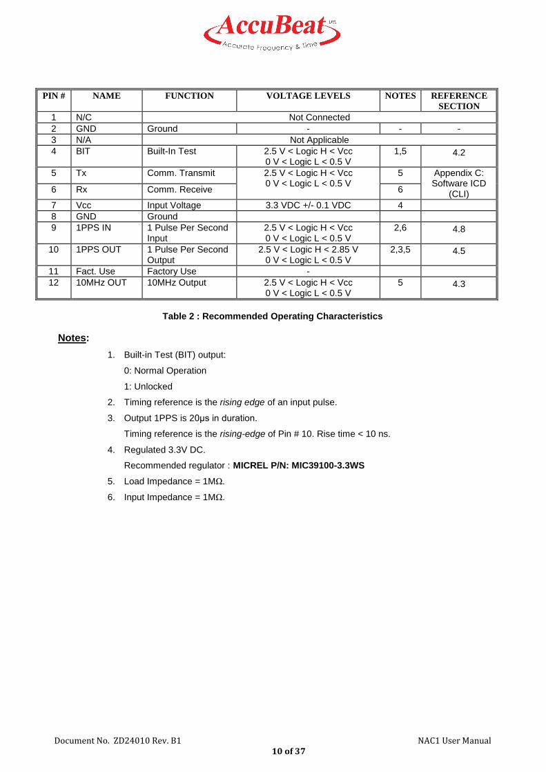
The NAC1 pinout is shown above in Figure 1. The electrical function of each pin is defined in this section.
Refer to the Reference Section for a detailed functionality description of each pin.
Figure 1 : NAC1 Mechanical drawing and Pinout
Document No. ZD24010 Rev. B1 NAC1 User Manual 10 of 37
PIN # NAME FUNCTION VOLTAGE LEVELS NOTES REFERENCE
SECTION
1 N/C Not Connected
2 GND Ground - - -
3 N/A Not Applicable
4 BIT Built-In Test 2.5 V < Logic H < Vcc 0 V < Logic L < 0.5 V
1,5 4.2
5 Tx Comm. Transmit 2.5 V < Logic H < Vcc 0 V < Logic L < 0.5 V
5 Appendix C: Software ICD
(CLI) 6 Rx Comm. Receive 6
7 Vcc Input Voltage 3.3 VDC +/- 0.1 VDC 4
8 GND Ground
9 1PPS IN
1 Pulse Per Second Input
2.5 V < Logic H < Vcc 0 V < Logic L < 0.5 V
2,6 4.8
10 1PPS OUT
1 Pulse Per Second Output
2.5 V < Logic H < 2.85 V 0 V < Logic L < 0.5 V
2,3,5 4.5
11 Fact. Use Factory Use -
12 10MHz OUT 10MHz Output 2.5 V < Logic H < Vcc 0 V < Logic L < 0.5 V
5 4.3
Table 2 : Recommended Operating Characteristics
Notes:
1. Built-in Test (BIT) output:
0: Normal Operation
1: Unlocked
2. Timing reference is the rising edge of an input pulse.
3. Output 1PPS is 20μs in duration.
Timing reference is the rising-edge of Pin # 10. Rise time < 10 ns.
4. Regulated 3.3V DC.
Recommended regulator : MICREL P/N: MIC39100-3.3WS
5. Load Impedance = 1MΩ.
6. Input Impedance = 1MΩ.
Document No. ZD24010 Rev. B1 NAC1 User Manual 11 of 37
3. Evaluation Kit
The Evaluation Kit enables the developer top easily evaluate and test the NAC1.
It includes all of the necessary hardware, software, and cabling to facilitate validation of performance
and software interface development.
The Evaluation Kit (AccuBeat P/N: AA50766) contains the following items:
1. Evaluation Board (AccuBeat P/N: AA50666).
2. CD-ROM: Graphic User Interface- GUI (AccuBeat P/N: SW50051).
3. Optional - 1PPS Input reference (AccuBeat P/N: AR133A-00).
4. USB to Serial Cable (AccuBeat P/N: ZE00314).
5. Protective sheet (AccuBeat P/N: MT30160).
3.1. Installing the NAC1 on the evaluation board
In an ESD- safe environment carefully remove the NAC1 and the evaluation board from their ESD
protective bags. Note that the NAC1 pinout is “keyed” (see Figure 1) so the NAC1 can only be
inserted in the proper orientation.
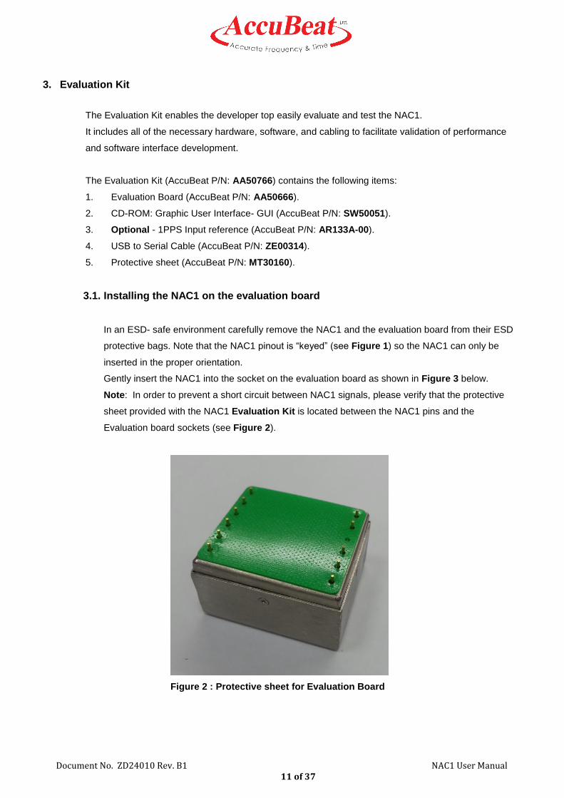
Gently insert the NAC1 into the socket on the evaluation board as shown in Figure 3 below.
Note: In order to prevent a short circuit between NAC1 signals, please verify that the protective
sheet provided with the NAC1 Evaluation Kit is located between the NAC1 pins and the
Evaluation board sockets (see Figure 2).
Figure 2 : Protective sheet for Evaluation Board

Document No. ZD24010 Rev. B1 NAC1 User Manual 12 of 37
Figure 3 : NAC1 on Evaluation board
3.2. Installing the NAC1 GUI software
The AccuBeat NAC1 GUI software (P/N: SW50051) provides a convenient graphical user interface
(GUI) for monitoring and controlling the NAC1.
After quick installation of the drivers, it will run on any PC running Microsoft Windows® XP or Windows®
7 and having at least one available RS232 (COM) or USB port. Note that multiple NACs can be
monitored from a single PC, provided additional COM ports are available.
To install the NAC1 GUI software, insert the provided CD-ROM into the CD drive of the PC. The
installation will not start automatically.
Please browse to the CD-ROM drive in Windows Explorer. In the GUI Drivers directory you may find
two .exe files.
For both files please perform the following procedure:
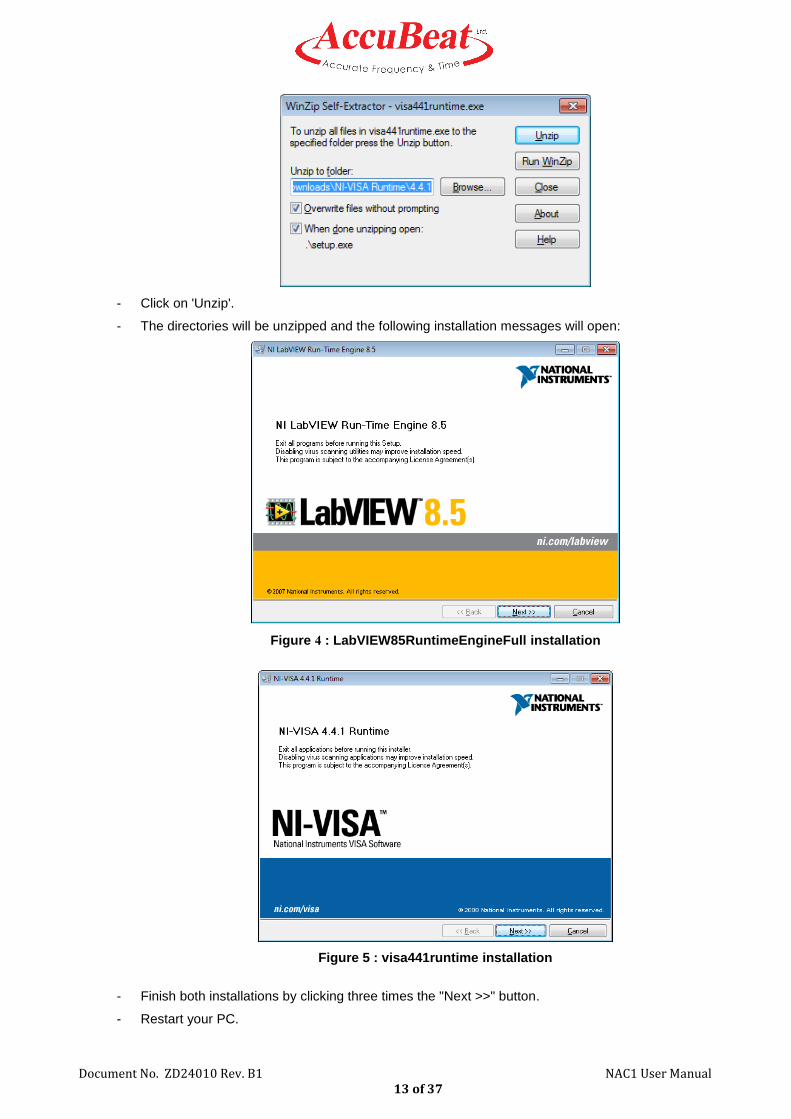
- Double-click on visa441runtime.exe / LabVIEW85RuntimeEngineFull.exe.
- The following message will open:
- Click on 'OK'.
- The following Unzip message will open:
Document No. ZD24010 Rev. B1 NAC1 User Manual 13 of 37
- Click on 'Unzip'.
- The directories will be unzipped and the following installation messages will open:
Figure 4 : LabVIEW85RuntimeEngineFull installation
Figure 5 : visa441runtime installation
- Finish both installations by clicking three times the "Next >>" button.
- Restart your PC.
Document No. ZD24010 Rev. B1 NAC1 User Manual 14 of 37
- Browse to the CD-ROM drive in Windows Explorer. Open the SW50051- Graphical User Interface
(GUI) for NAC1 customer directory and double-click on NAC1 Customer GUI.exe to open the
NAC1 GUI.
3.3. Cabling
Connect the provided RS-232 cable between the evaluation board and the COM port on the PC. On
laptops without an available COM port, a USB-to-RS232 adapter might work.
We recommend using the USB to Serial adapter (Support RS232 Serial communication) that was
supplied with the NAC1 Evaluation Kit.
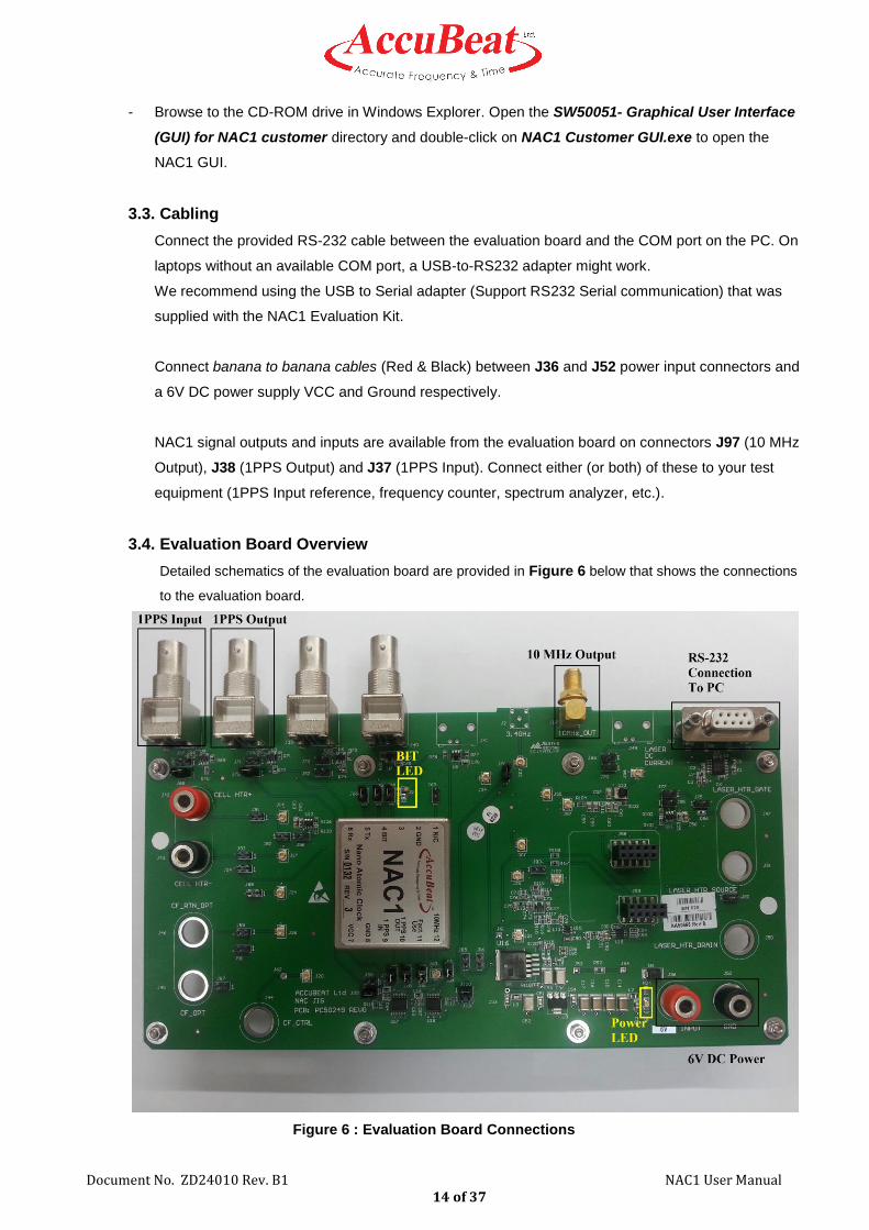
Connect banana to banana cables (Red & Black) between J36 and J52 power input connectors and
a 6V DC power supply VCC and Ground respectively.
NAC1 signal outputs and inputs are available from the evaluation board on connectors J97 (10 MHz
Output), J38 (1PPS Output) and J37 (1PPS Input). Connect either (or both) of these to your test
equipment (1PPS Input reference, frequency counter, spectrum analyzer, etc.).
3.4. Evaluation Board Overview
Detailed schematics of the evaluation board are provided in Figure 6 below that shows the connections
to the evaluation board.
Figure 6 : Evaluation Board Connections

Document No. ZD24010 Rev. B1 NAC1 User Manual 15 of 37
10 MHz Output (SMA) – The NAC1 output is a 10MHz, CMOS 0-3.3VDC waveform.
6V DC Power Input – Input power to the evaluation board is provided from an external power supply
through twisted pair banana cables. The use of a current limiter to 2A is recommended.
RS232 Connection (D9) –The evaluation board provides a level shifter (U1), which converts the NAC1
0-3.3 VDC serial interface to the RS232 standard +/- 12 V for direct interface with a PC COM port.
Connect the test fixture (J22) to a PC with a standard (non-Null) DB9F-DB9F RS232 cable. To avoid
problems, please use the proper cable which is provided by AccuBeat with the Evaluation Kit.
BIT Lock Indicator LED – Indicates normal operation following initial acquisition of the clock signal.
Note that this is the logical complement of the BIT output (NAC1 Pin # 4).
Power LED – Indicates the state of the external power supply.
1PPS Input (BNC) – The 1PPS input connection to the evaluation board accepts a 1PPS reference of
arbitrary amplitude (logic high: 2.5V < Vin < 5V) and passes it directly to the NAC1.
1PPS Output (BNC) –The 1PPS output can be buffered by a CMOS 0-3.3 V logic gate on the
evaluation board. For this option please transfer J99 Jumper to J98 Header.
Note: Do not change the configuration of the other JUMPERs connectors.
Document No. ZD24010 Rev. B1 NAC1 User Manual 16 of 37
3.5. Initial Start Up
3.5.1. Initial Power-On
Make sure NAC1 is placed on its socket on the Evaluation board with the protective sheet.
Connect the Evaluation board voltage input to the Power Supply.
Connect power and RS232 to the Evaluation Board as described in Section 3.3.
Make sure the simulated COM port number is known to you.
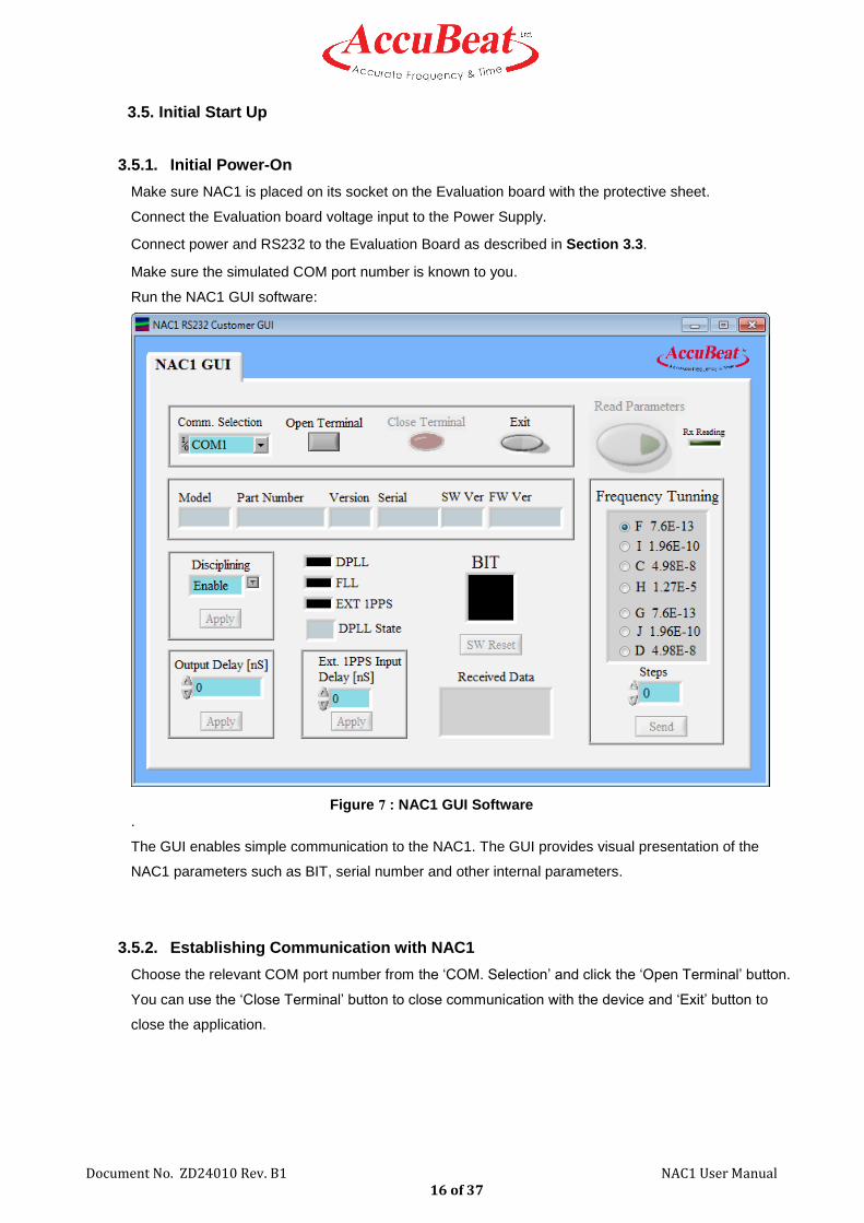
Run the NAC1 GUI software:
Figure 7 : NAC1 GUI Software .
The GUI enables simple communication to the NAC1. The GUI provides visual presentation of the
NAC1 parameters such as BIT, serial number and other internal parameters.
3.5.2. Establishing Communication with NAC1
Choose the relevant COM port number from the ‘COM. Selection’ and click the ‘Open Terminal’ button.
You can use the ‘Close Terminal’ button to close communication with the device and ‘Exit’ button to
close the application.

Document No. ZD24010 Rev. B1 NAC1 User Manual 17 of 37
3.5.3. Basic NAC1 GUI Features
The ‘Read Parameters’ button triggers the read of the NAC1 status and setup. The ‘Rx Reading’
indicator will be lit during the process of data acquiring.
The ‘Received Data’ window is basically used for the visual confirmation of the last issued command.
When the reading of parameters is completed, the updated data will be displayed on the GUI screen.
Note: After power up, start-up scripts will operate for 180 seconds. You cannot communicate with
NAC1 until the start-up scripts will end.
‘BIT’ (Built-In Test) indicates the overall status of the NAC1 control loops and readiness to function.
See also ‘UMR’ command description (Appendix C: Software ICD (CLI)) and Section 4.2 for more
information.
The ‘SW Reset’ button performs NAC1 Soft Reset, which is equivalent to a power cycle.
See also the ‘RST’ command description (Appendix C: Software ICD (CLI)).
The ‘Disciplining’ dialog allows controlling the disciplining process. The default setting is ‘Enable’.
Selecting ‘Disable’ will disable the disciplining, effectively switching NAC1 to Holdover state, regardless
to the 1PPS input status.
See the ‘SDM’ command description (Appendix C: Software ICD (CLI)) and Section 5 for more
information.
The ‘Output Delay’ dialog allows deferring the ‘1PPS Output’ phase by the specified number of nano-
seconds. This is a pure administrative function and doesn’t affect the disciplining algorithm.
See also the ‘SPD’ command description (Appendix C: Software ICD (CLI)) for more information.
The ‘Ext. 1PPS Input Delay’ dialog allows deferring the ‘1PPS Input’ phase by the specified number of
nano-seconds.
See also the ‘SED’ command description (Appendix C: Software ICD (CLI)) for more information.
The VER CLI instruction can be used to remotely identify the unit.
The instruction returns the unit part number (for example: NAC1), S/W and F/W versions, and the
unit’s serial number.
See also the ‘VER’ command description (Appendix C: Software ICD (CLI)) for more information.

Document No. ZD24010 Rev. B1 NAC1 User Manual 18 of 37
3.5.4. Frequency Tuning
The ‘Frequency Tuning’ dialog allows tuning the NAC1 microwave synthesizer by applying corrections
or setting an explicit frequency value. Corrections are sent in steps of 7.6E-13, 1.96E-10 or 4.98E-8 and
can be positive or negative with an arbitrary number of steps. Moreover, corrections can be applied for
the current session only (until power down) or forever. In the latter case the correction value affects the
base frequency, stored in a non-volatile memory. Every new correction is added to the base frequency.
See also the ‘RFC’ command description (Appendix C: Software ICD (CLI)) and Section 4.4 for
more information.

Document No. ZD24010 Rev. B1 NAC1 User Manual 19 of 37
4. Functional Description
This chapter provides an overview of the operation principles of a Rubidium Frequency Standard and
describes the main features in the NAC1 unit.
4.1. Principles of Operation
Atomic Clocks, the most accurate man-built machines, have been commercially available for over 40
years. Recent developments in atomic clocks technology have enabled a substantial reduction of size
and power consumption of these clocks, using the phenomenon of Coherent Population Trapping
(CPT), with alkali atoms such as Rubidium and Cesium. The CPT utilizes the transparency of an
atomic vapor cell, which is created when illuminated by two laser beams that differ in their frequency
(wavelength) by an amount that equals the hyperfine transition frequency of a Rubidium (@ ~6.8GHz
) or Cesium (at@ ~9.2GHz ). Instead of using 2 lasers one uses a single laser, which is modulated by
half the hyperfine frequency synthesized from a local crystal oscillator, thereby creating two
sidebands. When the separation between the sidebands exactly equals the hyperfine frequency, the
vapor becomes transparent. One uses this transparency to lock the local crystal oscillator (that
provides the clock output) to the atomic line. With this technique one gets rid of the conventional
lamp and resonance microwave cavity which are being used in the traditional Rubidium Frequency
Standard technology, thereby saving substantial size and power.
AccuBeat’s NAC1 utilizes a novel and unique scheme where numerous servo-loops are operating
simultaneously to stabilize all the key parameters of the clock, and where the sensors of the loops
origin from the atomic vapor. This results in an improved stability of the clock’s output and low
sensitivity to disturbances. In addition, the vapor cell in NAC1 is based on a proven traditional glass
technology which has been used in Rubidium Clocks for dozens of years. This assures very high
reliability and confidence in the design. For the same reason AccuBeat selected to use Rubidium
rather than Cesium due to the long Rubidium heritage in vapor cell atomic clocks (Cesium is normally
used in atomic beam clocks which deploy a totally different approach).
A detailed block diagram of the NAC1 is provided in Figure 8 below:
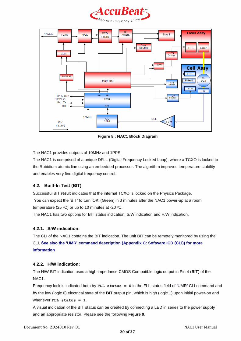
Document No. ZD24010 Rev. B1 NAC1 User Manual 20 of 37
Figure 8 : NAC1 Block Diagram
The NAC1 provides outputs of 10MHz and 1PPS.
The NAC1 is comprised of a unique DFLL (Digital Frequency Locked Loop), where a TCXO is locked to
the Rubidium atomic line using an embedded processor. The algorithm improves temperature stability
and enables very fine digital frequency control.
4.2. Built-In Test (BIT)
Successful BIT result indicates that the internal TCXO is locked on the Physics Package.
You can expect the ‘BIT’ to turn ‘OK’ (Green) in 3 minutes after the NAC1 power-up at a room
temperature (25 ºC) or up to 10 minutes at -20 ºC.
The NAC1 has two options for BIT status indication: S/W indication and H/W indication.
4.2.1. S/W indication:
The CLI of the NAC1 contains the BIT indication. The unit BIT can be remotely monitored by using the
CLI. See also the ‘UMR’ command description (Appendix C: Software ICD (CLI)) for more
information
4.2.2. H/W indication:
The H/W BIT indication uses a high-impedance CMOS Compatible logic output in Pin 4 (BIT) of the
NAC1.
Frequency lock is indicated both by FLL status = 0 in the FLL status field of 'UMR' CLI command and
by the low (logic 0) electrical state of the BIT output pin, which is high (logic 1) upon initial power-on and
whenever FLL status = 1.
A visual indication of the BIT status can be created by connecting a LED in series to the power supply
and an appropriate resistor. Please see the following Figure 9.

Document No. ZD24010 Rev. B1 NAC1 User Manual 21 of 37
Figure 9 : BIT LED indication
4.3. 10 MHz Output Characteristics
The buffered CMOS clock output at 10 MHz is provided on Pin # 12 of the NAC1. The output series
impedance is 200 Ω. For reference, the output driver circuit of the NAC1 is shown below in Figure 10.
Figure 10 : NAC1 10MHz Output Driver
The NAC1 is designed for embedded low-power applications, i.e. it is expected to drive a high
impedance input, not a 50 Ω measurement instrument or transmission line. If a high-level (high-
power) output driver is required, an external driver circuit should be implemented, such as the one
implemented on the Evaluation Board. See Figure 11 below.
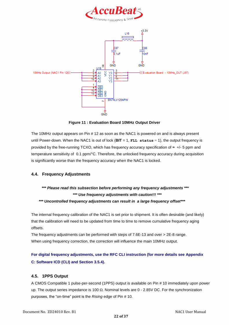
Document No. ZD24010 Rev. B1 NAC1 User Manual 22 of 37
Figure 11 : Evaluation Board 10MHz Output Driver
The 10MHz output appears on Pin # 12 as soon as the NAC1 is powered on and is always present
until Power-down. When the NAC1 is out of lock (BIT = 1, FLL status = 1), the output frequency is
provided by the free-running TCXO, which has frequency accuracy specification of ≈ +/- 5 ppm and
temperature sensitivity of 0.1 ppm/°C. Therefore, the unlocked frequency accuracy during acquisition
is significantly worse than the frequency accuracy when the NAC1 is locked.
4.4. Frequency Adjustments
*** Please read this subsection before performing any frequency adjustments ***
*** Use frequency adjustments with caution!!! ***
*** Uncontrolled frequency adjustments can result in a large frequency offset***
The internal frequency calibration of the NAC1 is set prior to shipment. It is often desirable (and likely)
that the calibration will need to be updated from time to time to remove cumulative frequency aging
offsets.
The frequency adjustments can be performed with steps of 7.6E-13 and over > 2E-8 range.
When using frequency correction, the correction will influence the main 10MHz output.
For digital frequency adjustments, use the RFC CLI instruction (for more details see Appendix
C: Software ICD (CLI) and Section 3.5.4).
4.5. 1PPS Output
A CMOS Compatible 1 pulse-per-second (1PPS) output is available on Pin # 10 immediately upon power
up. The output series impedance is 100 Ω. Nominal levels are 0 - 2.85V DC. For the synchronization
purposes, the “on-time” point is the Rising edge of Pin # 10.
Document No. ZD24010 Rev. B1 NAC1 User Manual 23 of 37
The 1PPS output is derived by digital division of the 10MHz reference frequency by a factor of 1E7. The
frequency stability and accuracy of the 1PPS output therefore reflects that of the 10MHz. Consequently,
when unlocked (BIT=1, FLL status = 1) the 1PPS Output stability reflects the free-running TCXO.
4.6. Rubidium free run
In the Rubidium free run mode, the output frequency accuracy is determined by the Rubidium
accuracy. In this case, only the FLL is activated.
4.7. Rubidium disciplined to 1PPS
In order to improve the frequency accuracy, the NAC1 is disciplined to an external 1PPS.
In this mode, both the FLL and the DPLL are activated.
When no 1PPS input is available, the unit operates in the Hold-Over mode.
To operate the disciplining mode, connect a 1PPS source (Section 4.8) to NAC1 Pin # 9 and
verify that the mode parameter of the 'SDM' CLI command is ‘1’ (for more details see Appendix
C: Software ICD (CLI)).
4.8. 1PPS Input
A Rubidium clock (locked or unlocked to GPS), Cesium clock or GPS receiver can be used as a 1PPS
source for the NAC1.
It is most important to use an accurate 1PPS source, since the NAC1 disciplines to the external 1PPS
source. If the 1PPS input is accurate, then the NAC1 is accurate as well.
AccuBeat has a variety of GPS-disciplined Rubidium clock products, which can function as highly
accurate 1PPS source. For additional information, please contact AccuBeat sales department or visit us
online at www.accubeat.com.
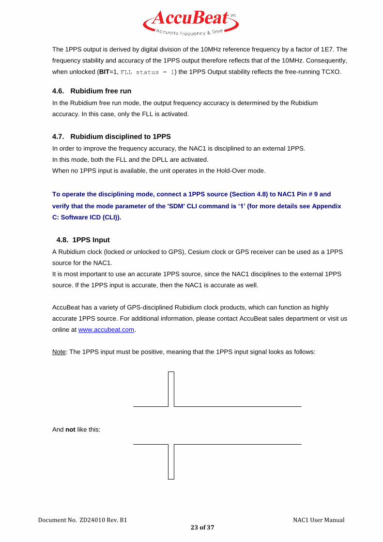
Note: The 1PPS input must be positive, meaning that the 1PPS input signal looks as follows:
And not like this:
Document No. ZD24010 Rev. B1 NAC1 User Manual 24 of 37
5. Disciplining Mode
This chapter provides a general overview on the disciplining algorithm implemented in the NAC1 clock.
The 1PPS disciplining uses a DPLL (Digital Phase Locked Loop) algorithm to discipline the Rb frequency
to an external 1PPS.
A phase meter is implemented within the NAC1 for improved synchronization (< 100 ns) as well as for
frequency calibration of the NAC1. The phase meter measures the time difference between the internal
NAC1 1PPS (Pin #10) and the externally applied reference 1PPS (Pin #9). The phase meter measures
the relative phase between the NAC1 and the reference once per second with a resolution of 5 ns.
Based on the measurements of the phase meter, internal steering algorithms adjust the frequency of the
NAC1's microwave synthesizer so as to simultaneously steer both the phase and frequency to that of the
external reference.
The DPLL algorithm has 4 states:
DPLL State Condition
0 1PPS input is applied and disciplining mode is activated (‘SDM 1’)
1 1PPS input is applied and disciplining mode is activated (‘SDM 1’)
2 1PPS input is applied and disciplining mode is activated (‘SDM 1’)
3 1PPS input is not applied or disciplining mode is not activated (‘SDM 0’)
State 0:
The Rb 1PPS will be synchronized to the external 1PPS. During this phase, the Rb 1PPS will abruptly
synchronize to the external 1PPS. No frequency correction is sent to the clock by the DPLL algorithm.
In a standard unit the time for this state is about 15 minutes (under normal conditions such as continuous
1PPS input etc.).
State 1:
This state applies corrections to the clock frequency using the DPLL algorithm calculations. During this
phase, the DPLL uses unique parameters set applicable to state 1.
In a standard unit, the time for this state is about 60 minutes from power up (under normal conditions like
continuous1PPS input etc.).
State 2:
This state applies corrections to the clock frequency using the DPLL algorithm calculations. At this time
the DPLL uses unique parameters set relevant to state 2.
In a standard unit the clocks get to state 2 after completion of state 1 (under normal conditions like
continually 1PPS input existence etc).
State 3:
The clock is in Hold Over mode. No frequency corrections are sent to the clock.
Document No. ZD24010 Rev. B1 NAC1 User Manual 25 of 37
Passing from state 0 / 1 / 2 to state 3 is done by disconnecting the 1PPS input or by setting the
disciplining mode to 'Off' (‘SDM 0’).
Exit from state 3 (Hold Over) to active disciplining is done by connecting a 1PPS input and setting the
disciplining mode to 'On' (‘SDM 1’).
Indication of the DPLL state appears in the UMR instruction field number 6 (‘DPLL STATE‘).
Hold Over declaration is made as follows:
In case of 1PPS disconnection – the HW waits for two sequential cycles and verifies that no 1PPS
input exists. After two cycles the HW produces the SW indication that no 1PPS input is detected. The
SW waits for another two sequential cycles to determine that no 1PPS input exists, and the NAC1
mode is set to Hold Over (state 3).
In case the user sends a ‘SDM 0’ instruction, the NAC1 will immediately be set to Hold Over (state
3).
Note: When using the disciplining mode, the NAC1 frequency accuracy is derived from the accuracy of
the 1PPS input source. Therefore, use only 1PPS input that is generated from accurate and stable
sources.
In case that during the operation the 1PPS source becomes invalid (for example: no satellites receiving in
the GPS receiver), disconnect the 1PPS input or send SDM = 0 instruction to the NAC1.
Please note that when resetting the unit (CLI instruction ‘RST Y’) the DPLL algorithm is also restarted.

Document No. ZD24010 Rev. B1 NAC1 User Manual 26 of 37
6. Appendices
Appendix A: Mechanical ICD
Figure 12 : Mechanical ICD (NAC1004)

Document No. ZD24010 Rev. B1 NAC1 User Manual 27 of 37
Appendix B: Electrical ICD
.
PIN # Function Electrical Characteristics
Block Diagram
12 10MHz Output
CMOS, 3.3V@1MΩ
NAC1
10MHz 3.3 VDC
COM
1PPS OUT1PPS IN
BIT
10 1PPS Output CMOS compatible, 3.3V@1MΩ Rise / Fall time: <10 ns, Pulse width: 20 µs
9 1PPS Input CMOS, 3.3V@1MΩ
4 Built in test
(BIT) CMOS compatible, 3.3V@1MΩ '0' = Normal operation, '1' = Alarm
7 Power input 3.3±0.1 VDC
5,6 Serial
Comm.
Control and monitor interface
RS232, format CMOS compatible, 3.3V@1MΩ, 115200BPS
Table 3 : Electrical ICD (NAC1004)

Document No. ZD24010 Rev. B1 NAC1 User Manual 28 of 37
Appendix C: Software ICD (CLI)
C.1. General Comments on the CLI Commands The CLI is based on ASCII characters. Default protocol configuration:
- Baud Rate: 115,200 - Parity: None - Start Bit: 1 - Data Bits: 8 - Stop Bit: 1 - Flow Control: None
Each setup command is used to:
1. Set the appropriate parameters according to the full syntax. 2. View the current system parameters (in this case only the command name is
entered).
For example:
SEO Y<cr> - Will set the echo ON when used with a terminal application to configure the system mode.
SEO<cr> - Will cause the system to reply "SEO Y" to indicate that the echo mode is used in the system.

Document No. ZD24010 Rev. B1 NAC1 User Manual 29 of 37
General notes: 1. The setup commands can be sent in one of the following formats:
o Command<space><data><CR> o Command<space><data><LF> o Command<space><data><CR><LF> o Command<space><data><LF><CR>
Note: The command parsing will start right after the <CR> or <LF>. In the 3rd and 4th forms above the <LF> and <CR> will be ignored.
2. In case of CLI commands with several parameters, each parameter is separated from each other with the comma sign (',').
3. Parameters can be skipped by typing the ',' only without any value following them. In the case where there is no intention to change the trailing parameters, they can be simply omitted.
4. All values should be in ASCII format. 5. If the communication is with a PC, the recommendation is to work with SEO N. 6. If the communication is interactive with a user (for example communication using a Hyper
Terminal) the recommendation is to work with SEO Y. 7. a. When SEO N is applied, the output (response from the unit) to all CLI commands will be in
the following form: Command<space><data><CR><LF>
b. When SEO Y is applied, the output (response from the unit) to all CLI commands will be in the following form:
Command<CR><CR><LF> Command<20><data><CR><LF><3E><20> Note: The first Command<CR> is the ECHO of the received command.
8. Error messages: a. If the operator enters characters that do not match one of the specific CLI commands the following error message will be reported: "Unknown command". b. If the operator enters characters that do not match one of the parameters in a CLI command the following error message will be reported: "Invalid command"
9. Case sensitivity: Both commands and their parameters can be entered in uppercase or lowercase letters.

Document No. ZD24010 Rev. B1 NAC1 User Manual 30 of 37
C.2. CLI Commands Summary
# Command Name
1 VER - Report Version
2 SEO - Set Echo ON/OFF
3 RST - Reset Unit
4 RFC - Rubidium Frequency Correct
5 SDM - Set Disciplining Mode
6 SED - Set External 1PPS input Propagation Delay
7 SPD - Set Output Propagation Delay
8 UMR - User Monitor Report
Document No. ZD24010 Rev. B1 NAC1 User Manual 31 of 37
C.3. General Commands
VER – Report Version
VER
This command generates a version report in the following form: VER Model,PN,Mver,Sn,SW_Ver,FW_Ver
Model - Unit model (Up to 4 characters. Example - "NAC1")
PN - Part number (Up to 7 characters. Example - "NAC1-00")
Mver - Model revision (Up to 2 characters. Example - "A1")
Sn - Serial number (Up to 6 characters. Example - "000000")
SW_Ver - Software Version (Up to 5 characters. Example - "01.00")
FW_Ver - Firmware Version (Up to 5 characters. Example - "01.00")
SEO – Set Echo ON/OFF
SEO mode
mode = Y set Echo ON
N set Echo OFF (Default)
This command is mainly used to set echo ON when used with a terminal to configure the system. The Local Echo mode is not stored in the system FRAM and restores to its defaults upon reset or power cycle.
RST – Reset Unit
RST Y
Y = Y, the SW will be reset. The unit locking process will be restarted.

Document No. ZD24010 Rev. B1 NAC1 User Manual 32 of 37
C.4. Clock Frequency Setting
RFC – Rubidium Frequency Correct
Use this CLI command to set the frequency correction. RFC cmd,x
cmd - Rubidium frequency correction step value
F - Steps of 7.6E-13 (will also be saved in a non-volatile memory). I - Steps of 1.94E-10 (will also be saved in a non-volatile memory). G - Steps of 7.6E-13 (will be saved in a volatile memory). J - Steps of 1.94E-10 (will be saved in a volatile memory).
x - Number of frequency change steps, as a signed value (-127 ÷ 127).
Note: Use frequency corrections with caution! Uncontrolled correction can cause an offset to the clock frequency.

Document No. ZD24010 Rev. B1 NAC1 User Manual 33 of 37
C.5. 1PPS Disciplining
SDM – Set Disciplining Mode
Use this CLI command to set disciplining mode. SDM mode
mode = 0 , DPLL OFF (Not disciplined, Open loop).
1 , DPLL ON (Disciplined, Default). The parameter will be saved in a non-volatile memory. When SDM set to 0 (‘SDM 0’) the clock will ignore the 1PPS input and will be in ‘Hold Over’ mode.
SED – Set External 1PPS input Propagation Delay
Use this CLI command to set external 1PPS input propagation delay.
SED x
x = Delay in ns units (Range: -25,000 ÷ 25,000ns, Default: 0ns).
The parameter will be saved in a non-volatile memory.
SPD – Set Output Propagation Delay
Use this CLI command to set external 1PPS output propagation delay.
SPD x
x = Delay, in ns units. (Range: -500,000,000 ÷ 500,000,000 ns, Default: 0ns).
The parameter will be saved in a non-volatile memory.
Document No. ZD24010 Rev. B1 NAC1 User Manual 34 of 37
C.6. Monitor Commands
UMR - User Monitor Report
UMR BIT,N/A,DPLL_Mode,N/A,FLL_mode,DPLL_State,EXT_PPS
BIT - BIT status (indicates the FLL status: 0 = BIT OK, 1 = BIT Failed) N/A - Not Applicable DPLL_Mode - DPLL Loop (1=On, 0=Off)
1 - Disciplining mode is enabled (‘SDM 1’). 0 - Disciplining mode is disabled (‘SDM 0’).
N/A - Not Applicable
FLL_mode - FACTORY USE (FLL Loop mode: 1 = On, 0 = Off) DPLL_State - DPLL state
The DPLL state value can be one of the following: 0, 1, 2 – 1PPS input exists and disciplining mode is enabled (‘SDM 1’).
3 – 1PPS input does not exist or disciplining mode is disabled (‘SDM 0’). EXT_PPS - External 1PPS status (1 = Exists, 0 = Does not exist).

Document No. ZD24010 Rev. B1 NAC1 User Manual 35 of 37
Appendix D: Specifications
PREL NAC1 - Nano Atomic Clock
PRELIMINARY SPECIFICATIONS
Phase noise (floor): -150dBc / Hz
Power Consumption: < 1.2W
Size: 32cc (41.1mm X 35.3mm X 22 mm)
Aging: <3E-10/month
Temp Stability: ±1E-9 / -20°C to 65°C
Outputs: 10 MHz , 1PPS
Supply voltage: 3.3 VDC
RS232 interface for monitoring and control
The NAC1 is the newest and smallest addition to AccuBeat’s line of Rubidium Frequency Standards. Incorporating proven traditional glass technology and based on Coherent Population Trapping (CPT), the NAC1 is an extremely small and compact atomic clock that has been designed as a board mounted component. NAC1 provides 10 MHz and 1PPS outputs and short term stability (Allan Deviation) of 2E-11 @ 100 seconds with aging of 3E-10/month at 25°C. The NAC1 has a RS232 interface for monitoring and control, a Built in Test (BIT) output and a warm-up time of typically 160 seconds. Measuring just 41.1mm X 35.3mm X 22mm and weighing only 75 grams and with a power consumption of less than 1.2 Watts, the new NAC1 is a Rubidium atomic clock especially suitable and designed for a wide range of portable applications.
Applications:
The NAC1 is specifically designed for low power applications such as:
GPS receivers UAV’s Autonomous sensors Backpack secure communication radios.
10MHz Output
CMOS compatible, 3.3V@1MΩ
1PPS
Output CMOS compatible, 3.3V@1MΩ Rise / Fall time: <10 ns, Pulse width: 20 µs
1PPS Input
CMOS, 3.3V@1MΩ
Rubidium Frequency Standard
Key Features
Descript ion
Inputs & Outputs
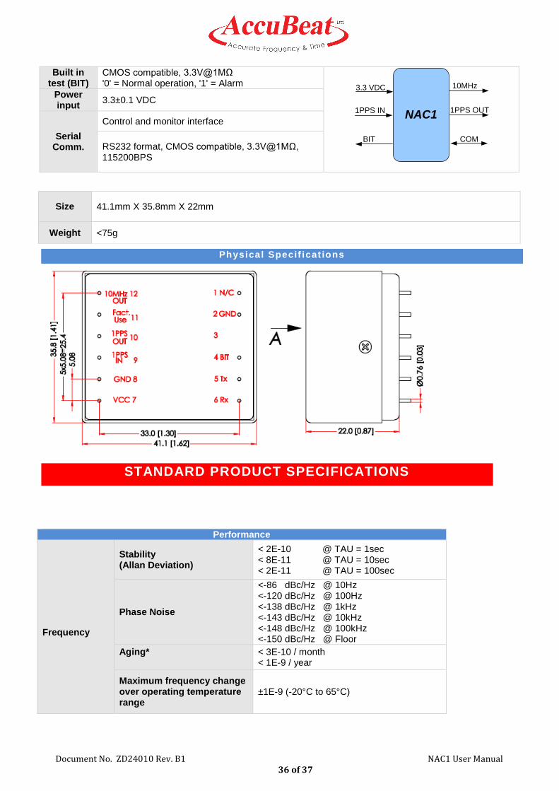
Document No. ZD24010 Rev. B1 NAC1 User Manual 36 of 37
Performance
Frequency
Stability (Allan Deviation)
< 2E-10 @ TAU = 1sec < 8E-11 @ TAU = 10sec < 2E-11 @ TAU = 100sec
Phase Noise
<-86 dBc/Hz @ 10Hz <-120 dBc/Hz @ 100Hz <-138 dBc/Hz @ 1kHz <-143 dBc/Hz @ 10kHz <-148 dBc/Hz @ 100kHz <-150 dBc/Hz @ Floor
Aging*
< 3E-10 / month < 1E-9 / year
Maximum frequency change over operating temperature range
±1E-9 (-20°C to 65°C)
Built in test (BIT)
CMOS compatible, 3.3V@1MΩ '0' = Normal operation, '1' = Alarm
NAC1
10MHz 3.3 VDC
COM
1PPS OUT1PPS IN
BIT
Power input
3.3±0.1 VDC
Serial Comm.
Control and monitor interface
RS232 format, CMOS compatible, 3.3V@1MΩ, 115200BPS
Size 41.1mm X 35.8mm X 22mm
Weight <75g
STANDARD PRODUCT SPECIFICATIONS
Physical Specif icat ions

Document No. ZD24010 Rev. B1 NAC1 User Manual 37 of 37
Digital Tuning (Through Serial communication)
Range: ±2E-8 Resolution: 7.6E-13
Initial offset at shipment ±5E-11
Time Accuracy
1PPS Sync. ±100nsec
Warm-up Warm-up Time (Time to BIT)
160s (Typ)
Power Consumption
Operation < 1.2W
Warm-up < 1.8W
Storage Temperature
-40°C to +90°C
No damage operating temperature
-40°C to 85°C but the clock is locked at -20°C to 65°C only
*After 30 days of continues operation
All specifications at 25ºC, Vcc =3.3VDC unless otherwise specified
Special Features Wave Form Output
Frequency AccuBeat P/N
Standard Square 10MHz NAC1004
Without pins #2,11 Square 10MHz NAC1C04
Description AccuBeat P/N
NAC1 Evaluation Kit AA50766
Evaluation Kit
How to Order


![Research Paper NAC1 attenuates BCL6 negative ... · sensitize cancer cells to anticancer agents [18]. Moreover, NAC1 regulates the expression of over 700 genes in ovarian cancer,](https://cdn.vdocument.in/doc/165x107/5f135aac92eff010750d1943/research-paper-nac1-attenuates-bcl6-negative-sensitize-cancer-cells-to-anticancer.jpg)


