Photograph: copyright IMEC
Nano-sized ceria abrasive for advanced polishing applications in IC manufacturingJoke De Messemaeker, Stijn Put, Daniël Nelis, Dirk Van Genechten,Paul Lippens, Yves Van Rompaey and Yvan Strauven
Umicore Group Research&Developement, Olen, Belgium
• Introducing Umicore nanomaterials• Nano-powder synthesis• Dispersion technology• Case study – nano-ceria for CMP applications
• CMP application• Development of nano-ceria for CMP
• Summary & conclusions
Outline

3i-SUP 2008 24-04-2008
The Umicore approach to materials technology
3

4i-SUP 2008 24-04-2008
Umicore today provides …
the automotive catalysts for almost 1 in 4 cars produced in the world
recycling services for electronic scrap, batteries and spent catalysts to gain over 20 different metals
the semiconductor substrates for more than 60% of all satellite solar cells in the last 2 years
key materials for the rechargeable batteries for more than 30% of all cell phones and laptops sold this year
Umicore in a nutshell …
15,000 people50 industrial locations worldwide1.9 B € revenue in 2006
Introducing Umicore

5i-SUP 2008 24-04-2008
Nano: Hype or future?
Technology miniaturization
Materials miniaturization
0.2 micronNickel Powder
Umicore started nano activities ~ 8 years ago
Nano creates a Win³ situation:• Device maker:
− Miniaturisation (e.g. MLCC) − Enables new technologies
• Supplier: − Added value products− Decommoditisation
• Society: − Sustainability: more function with less materials
6i-SUP 2008 24-04-2008
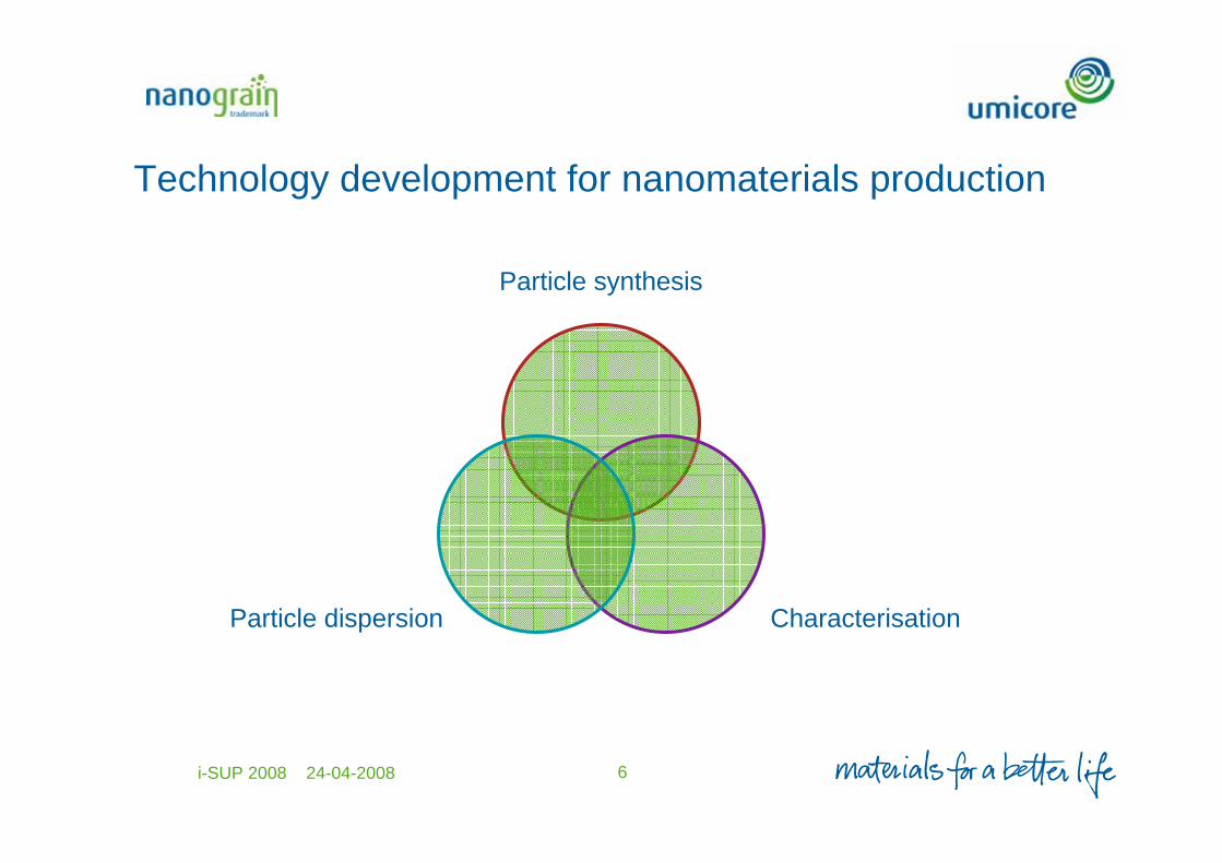
Technology development for nanomaterials production
Particle synthesis
CharacterisationParticle dispersion

Powder synthesis

8i-SUP 2008 24-04-2008
Particle synthesis and development
Particles or functional particles are developed in function of the application• Functionality• Quality• Cost
On the basis of this, a synthesis technology is developed, Umicore has developed a range of synthesis and production technologies for the development of nanomaterials
• Gas phase synthesis (evaporation + reaction + quenching)• Mainly for oxide materials
• Precipitation techniques• Milling techniques

9i-SUP 2008 24-04-2008
• large economy of scale• patented process
Process:Metal solution + reduction
Precipitated Metal
Umicore precipitation Technology

10i-SUP 2008 24-04-2008
Umicore NanoMaterials particles, oxides
NanoGrain® CeO2Doped TiO2 (Optisol®)
NanoGrain® In2O3 NanoGrain® ZrO2 Others
Anatase, Rutile, GeO2, ITO, doped ZnO, Al2O3, ...
ZnO (Zano®)

Dispersion technology
12i-SUP 2008 24-04-2008
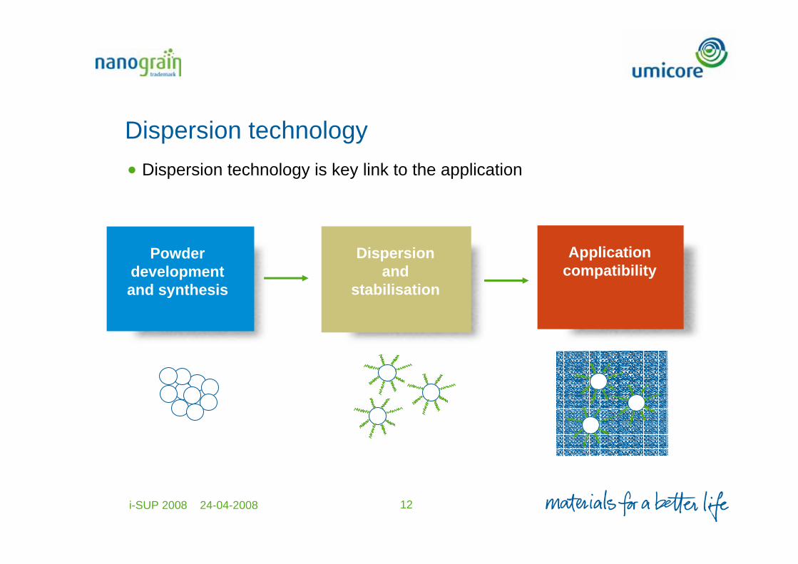
Dispersion technology
Powder development and synthesis
Applicationcompatibility
Dispersionand
stabilisation
• Dispersion technology is key link to the application

13i-SUP 2008 24-04-2008
Dispersion technology
• De-agglomeration of particles:• Apply the right amount of energy to obtain desired results
• Stabilisation e.g. with additives – need for compliance withapplication!
Low
• Used to prepare pre-mixes
• De-agglomeration not optimal
• Examples: •dissolver
Intermediate
• Low solids loading• De-agglomeration
• Examples:• ultrasonication• rotor-stator
High
• High solids loading• De-agglomeration and
milling
• Examples:• bead mills• ball mills

Photograph: copyright IMEC
Case study:
Nano-ceria for CMP applications
1 – CMP application
15i-SUP 2008 24-04-2008
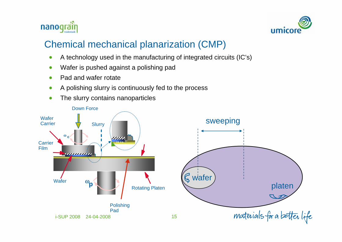
Chemical mechanical planarization (CMP)• A technology used in the manufacturing of integrated circuits (IC’s)• Wafer is pushed against a polishing pad• Pad and wafer rotate• A polishing slurry is continuously fed to the process• The slurry contains nanoparticles
Polishing Pad
Wafer
Slurry
Down Force
ω c
ωp
Wafer Carrier
Carrier Film
Rotating Platen
waferplaten
sweeping

16i-SUP 2008 24-04-2008
• More and smaller transisitors on single chip = increasing # interconnecting layers• Accumulated topology of different layers exceeds lithography depth of focus• Solution is planarisation of layers by CMP, invented by IBM in the 1980’s• Developed into enabler for many of the new technologies in e.g. Intel’s processers
CMP: an enabling technology in IC manufacturing
Planarized IC productNo CMP-used

17i-SUP 2008 24-04-2008
Si3N4
Si
SiO2
Si3N4
SiSiO2
Si3N4
Si
Example: shallow trench isolation (STI)
Si
Si3N4
SiO2
SiO2
SiO2
SiO2
Si
SiO2 SiO2Si
Si3N4
SiO2 SiO2
STI CMP slurriescontain ceria
Mask active areas and etch trench
Pre-oxidize trench
Field oxide deposition
Ceria CMP-step
Wet nitride etch

Photograph: copyright IMEC
Case study:
Nano-ceria for CMP applications
2 – Development of nano-ceria for CMP

19i-SUP 2008 24-04-2008
Objective and approach
Development of ceria particles with low defectivityfor STI CMP
• Development of synthesis route to control ceria properties• Testing of ceria particles with different properties in CMP• Impact of specific surface area• Impact of large particle tail• Impact of particle shape
• Feedback of CMP results to synthesis• Establishment of consistency for best product

20i-SUP 2008 24-04-2008
Ceria particle size/specific surface area
• Specific surface area in range 20 to 85 m²/gEquivalent average primary particle size range: 10 to 40 nm
• Primary particles not sintered: no hard agglomerates• 100 % cubic crystalline

21i-SUP 2008 24-04-2008
Control of particle morphology
Particle morphology can be controlled through processing conditions

22i-SUP 2008 24-04-2008
Ceria dispersion properties
Particle size distribution in dispersion determined by dispersion technique used
Technique A
Technique B
XDC measurements

23i-SUP 2008 24-04-2008
CMP evaluation
• Key performance parameters for STI CMP• High removal rate for SiO2• Smooth, defect free surface finish (= low defectivity)
• Stabilizer added to dispersions (no other additives)
• Pre and post CMP characterization• Film thickness: spectroscopic ellipsometry (ASET-F5, KLA Tencor)• Defectivity: dark field laser light scattering (SP-1, KLA Tencor)
• Defectivity evaluation• Minimum defect size 0.15 µm• Focus on scratches as particles can be removed during further
processing

24i-SUP 2008 24-04-2008
Impact of specific surface area
• Strong correlation between particle size and removal rate
• Lower defectivity for smaller particle size, but plateau below 20 nm
Removal rate Defectivity

25i-SUP 2008 24-04-2008
Effect of various coarse fraction removal techniques on large particle count and polishing results
• Large particle count controlled by coarse fraction removal technique
Removal rate Defectivity
A : reference (as sonicated) B..F : different techniques

26i-SUP 2008 24-04-2008
CMP Scratch Formation
pad
slurry
oxidized Cu
♦ Unwanted large particles dig too deep♦ Damage causing particles cannot be easily detected
♦ Excellent control of large particle tail required!
Cu substrate
Large particle > 1u
Scratch
Importance of large particle count for defects

27i-SUP 2008 24-04-2008
Impact of particle shape I
Sharp particleshave slightly better CMP performance than truncated particles

28i-SUP 2008 24-04-2008
Impact of particle shape II
Rounded particleslower removal rate & higher defectivity
Unexpected result!

29i-SUP 2008 24-04-2008
Final selected product
10 nm
• Adjusted particle size• Controlled large particle tail• Controlled morphology
• Excellent combination of removal rateand defectivity
• Excellent reproducibility• Low cost potential

30i-SUP 2008 24-04-2008
Consistency
• 5 Production batches (A thru E) tested in CMP
• Good consistency of CMP results

31i-SUP 2008 24-04-2008
Summary and conclusions
• Development of new nanomaterials for large scale productionrequires dispersion and application knowledge
• Gas phase synthesis process was developed to gain flexiblecontrol over particle size, distribution and morphology
• Nano-ceria particles for CMP were developed allowing• Better defectivity• Good removal rate• Good batch-to-batch and within-batch consistency