
Memory Systems for Embedded Applications
Chapter 4 (Sections 4.1-4.4)
1

Platform components
CPUs. Interconnect buses. Memory. Input/output devices.
Implementations: System-on-Chip (SoC) vs. Multi-Chip
Microcontroller vs. microprocessor
Commercial off-the-shelf (COTS) vs. custom FPGA & Platform FPGA
2

CPU Buses Mechanism for communication with memories and I/O
devices Bus components: signal wires with designated functions protocol for data transfers electrical parameters (voltage, current, capacitance, etc.) physical design (connectors, cables, etc.)
3
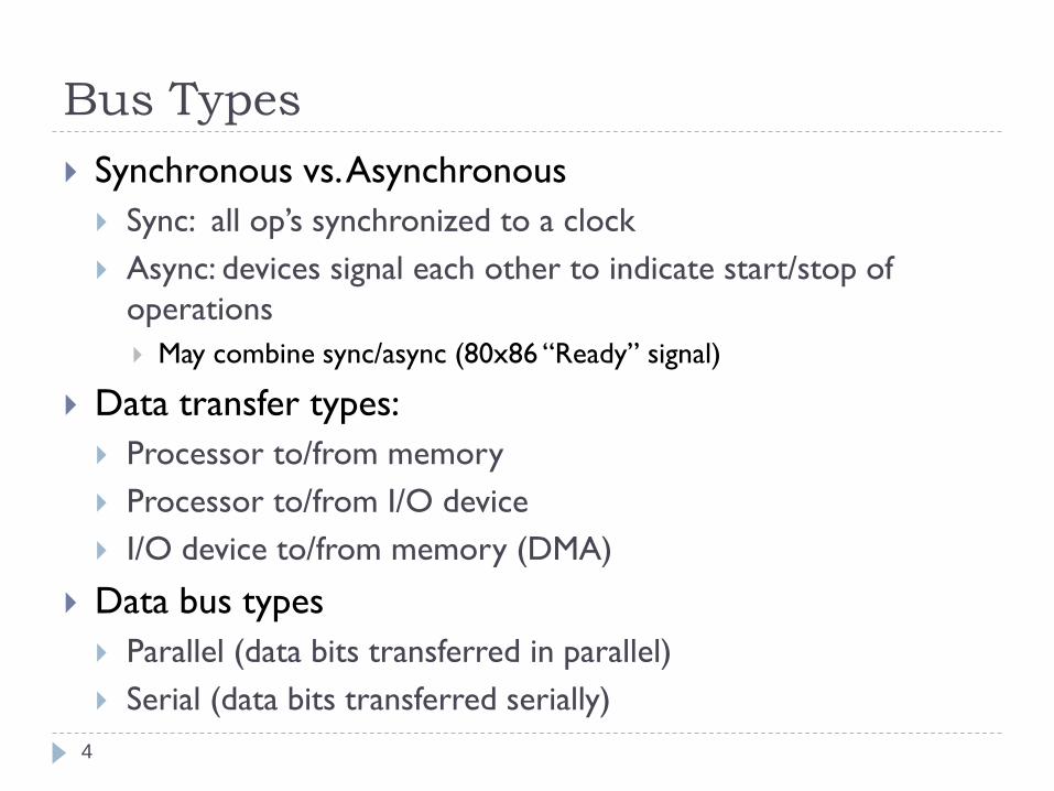
Bus Types Synchronous vs. Asynchronous Sync: all op’s synchronized to a clock Async: devices signal each other to indicate start/stop of
operations May combine sync/async (80x86 “Ready” signal)
Data transfer types: Processor to/from memory Processor to/from I/O device I/O device to/from memory (DMA)
Data bus types Parallel (data bits transferred in parallel) Serial (data bits transferred serially)
4

Typical bus data rates
Source: Peter Cheung “Computer Architecture & Systems Course Notes”
5

Hierarchical Bus Architecture
CPU CacheLocal
controllerMain Memory
System
bridge
USBController
Expansion
USB
LANController
DiskController
VideoController
USBDevice
IDE/SCSI
Mouse/Keyboard
Main Memory
6

ARM Advanced Microcontroller Bus Architecture (AMBA) On-chip interconnect specification for SoC Promote re-use by defining a common backbone for SoC
modules using standard bus architectures AHB – Advanced High-performance Bus (system backbone)
High-performance, high clock freq. modules Processors to on-chip memory, off-chip memory interfaces
APB – Advanced Peripheral Bus Lower performance requirements Low-power peripherals Reduced interface complexity
Others: ASB – Advanced System Bus (high performance alternate to AHB) AXI – Advanced eXtensible Interface ACE – AXI Coherency Extension ATB – Advanced Trace Bus
7

Example AMBA System
Joe Bungo (ARM): CPU Design Concept to SoC8

ARM CoreLink peripherals for AMBA
“CoreLink”(orange blocks)
Interconnect + memory controllerIP for Cortex/Mali
9
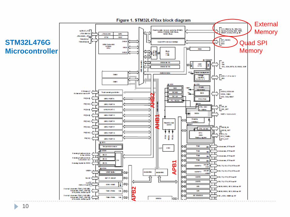
10
AHB
2AH
B1
APB
2
APB
1
STM32L476GMicrocontroller
External Memory
Quad SPIMemory

Microprocessor buses Clock provides
synchronization. R/W’ true when reading,
false when writing. May replace CLK and R/W
with RD and WR strobes
Address is a-bit bundle of address lines.
Data is n-bit bundle of data lines.
Data ready signals when n-bit data is ready.
11
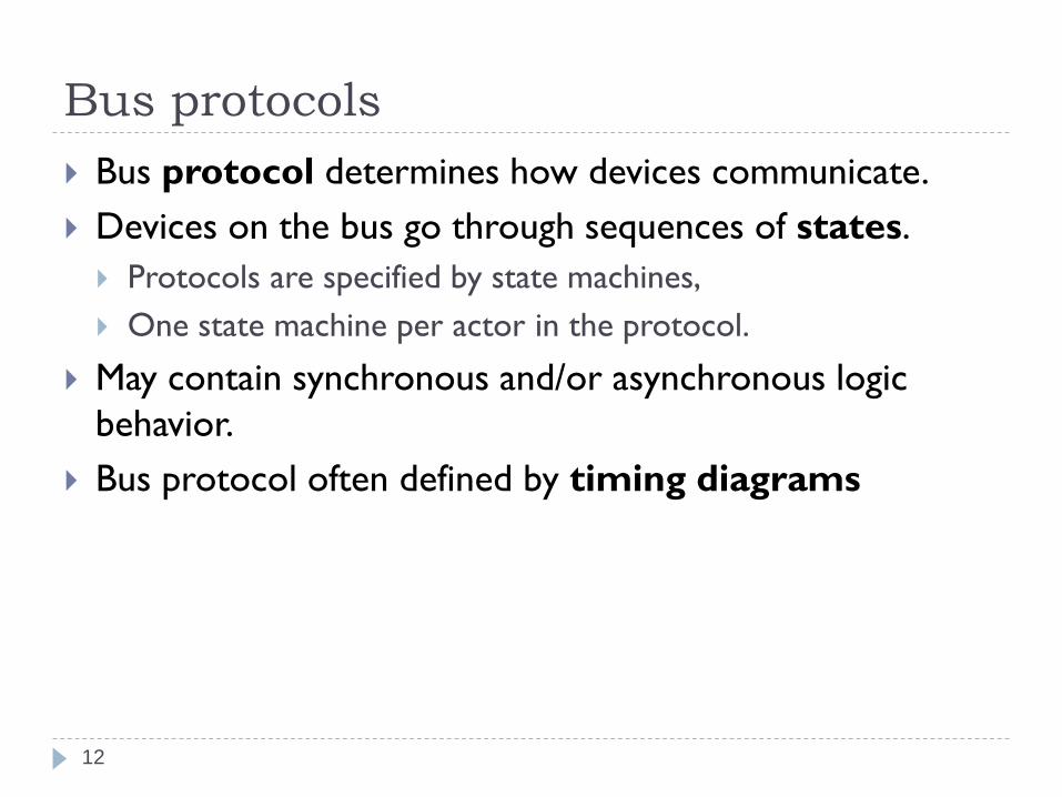
Bus protocols Bus protocol determines how devices communicate. Devices on the bus go through sequences of states. Protocols are specified by state machines, One state machine per actor in the protocol.
May contain synchronous and/or asynchronous logic behavior.
Bus protocol often defined by timing diagrams
12

Timing diagrams
13

Typical bus read and write timing
14

Bus wait state
15
Extend read/writecycle if memory slower thanCPU

Bus burst read
16
CPU sendsstart address,followed byburst of datafrom consecutiveaddresses

State diagrams for bus read
CPU DEVICE
Get data
Done
Adrs
Wait
Ack &Send data
Release ack
Adrs + CE
start
17
Ack?
No
Yes
Wait
Ready?
No
Yes
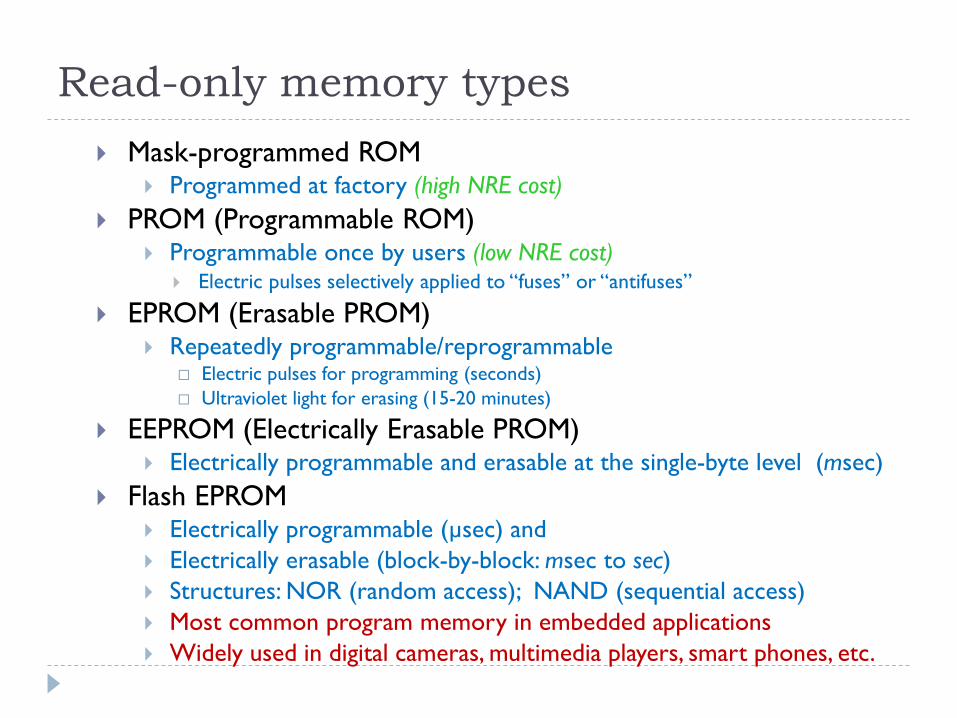
Read-only memory types Mask-programmed ROM
Programmed at factory (high NRE cost) PROM (Programmable ROM)
Programmable once by users (low NRE cost) Electric pulses selectively applied to “fuses” or “antifuses”
EPROM (Erasable PROM) Repeatedly programmable/reprogrammable
Electric pulses for programming (seconds) Ultraviolet light for erasing (15-20 minutes)
EEPROM (Electrically Erasable PROM) Electrically programmable and erasable at the single-byte level (msec)
Flash EPROM Electrically programmable (µsec) and Electrically erasable (block-by-block: msec to sec) Structures: NOR (random access); NAND (sequential access) Most common program memory in embedded applications Widely used in digital cameras, multimedia players, smart phones, etc.
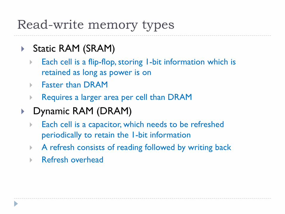
Read-write memory types
Static RAM (SRAM) Each cell is a flip-flop, storing 1-bit information which is
retained as long as power is on Faster than DRAM Requires a larger area per cell than DRAM
Dynamic RAM (DRAM) Each cell is a capacitor, which needs to be refreshed
periodically to retain the 1-bit information A refresh consists of reading followed by writing back Refresh overhead

ROM/RAM device organization
Size. 2n addressable
words Address width =
n = r + c
Aspect ratio. Data width d.
Memory arrayn r
c
d
Row #
Column #
Address
Data busconnection
Memory “organization” = 2n x d(from system designer’s perspective)
20
Row Decoder
ColumnDecoder

Memory address decoding
Select a sub-space of memory addresses A simple example
Microprocessor with 5 address bits (A4 … A0 ) 25 = 32 bytes addressable Assume 4 byte (4 x 8) memory chip Decodes two address bits (A1 A0 ) µP can address up to 8 chips (decode address bits (A4A3 A2) for chip enable
AB
0
1
2
3
Byte 0
Byte 1
Byte 2
Byte 3Enable
A0A1
DecodeUpper
Address Bits
A2A3A4
On-Chip Decoder Memory Array
Off-Chip Decoder

Typical generic SRAM
SRAM
CE#
OE#
Address
Data
CE# = chip enable: initiate memory access when activeOE# = output enable: drive Data lines when activeWE# = write enable: update SRAM contents with Data
(May have one R/W# signal instead of OE# and WE#)Multi-byte data bus devices have a byte-enable signal for each byte.
22
WE#

IS61LV51216-12T: 512K x 16 SRAM (on uCdragon board)
23
Byte Lane Select- Upper byte D15-8- Lower byte D7-0
Decoded A31-24
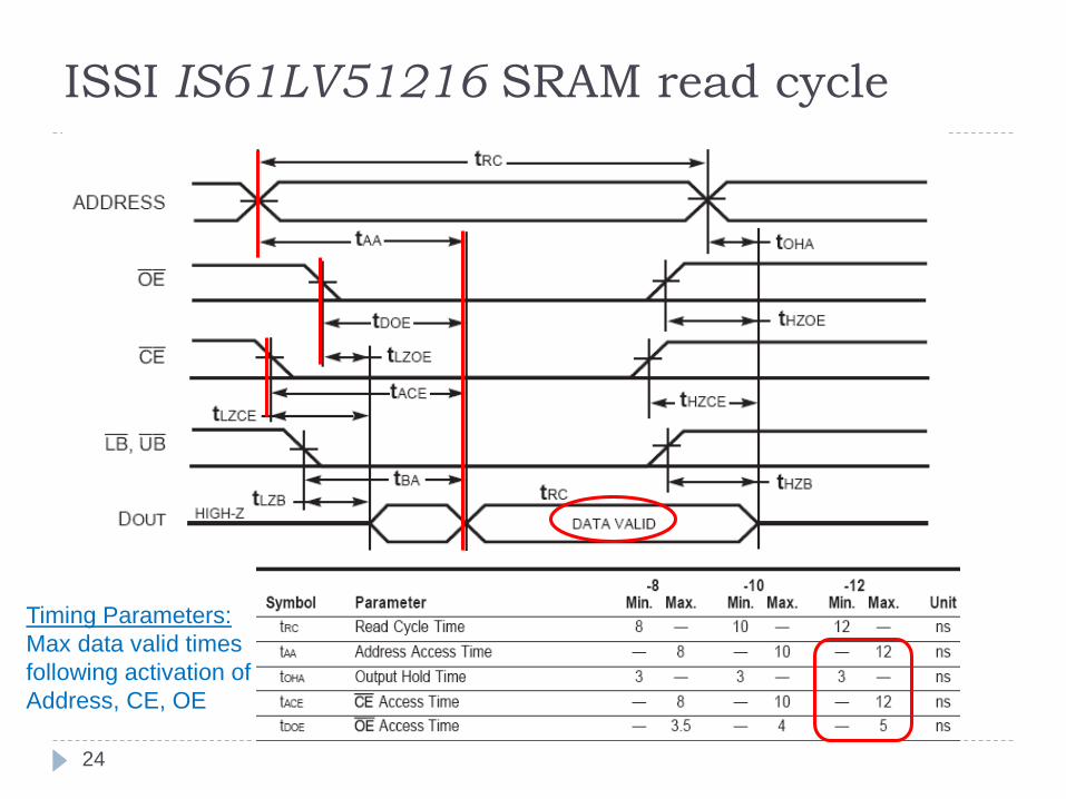
ISSI IS61LV51216 SRAM read cycle
24
Timing Parameters:Max data valid timesfollowing activation ofAddress, CE, OE
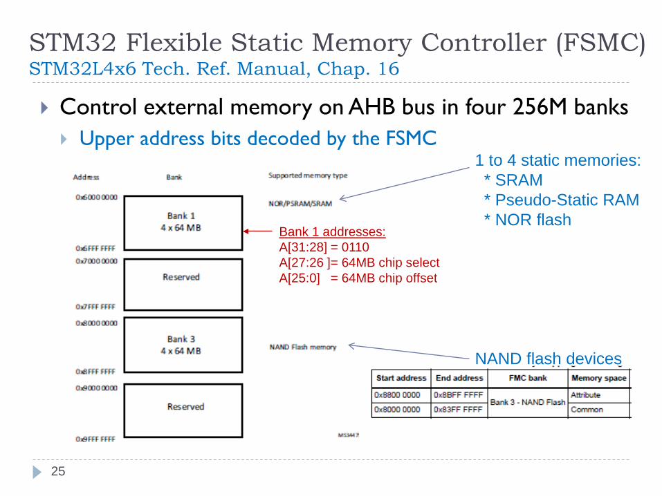
STM32 Flexible Static Memory Controller (FSMC) STM32L4x6 Tech. Ref. Manual, Chap. 16
Control external memory on AHB bus in four 256M banks Upper address bits decoded by the FSMC
1 to 4 static memories:* SRAM * Pseudo-Static RAM* NOR flash
NAND flash devices
25
Bank 1 addresses:A[31:28] = 0110A[27:26 ]= 64MB chip selectA[25:0] = 64MB chip offset
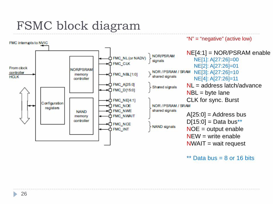
FSMC block diagram
26
“N” = “negative” (active low)
NE[4:1] = NOR/PSRAM enableNE[1]: A[27:26]=00NE[2]: A[27:26]=01NE[3]: A[27:26]=10NE[4]: A[27:26]=11
NL = address latch/advanceNBL = byte laneCLK for sync. Burst
A[25:0] = Address busD[15:0] = Data bus**NOE = output enableNEW = write enableNWAIT = wait request
** Data bus = 8 or 16 bits

FSMC “Mode 1” memory read
ADDSET/DATAST programmed in chip-select timing register (HCLK = AHB clock)
Other modes:
* Provide ADV(address latch/advance)
* Activate OE and WEonly in DATAST
* Multiplex A/Dbits 15-0
* Allow WAIT toextend DATAST
27
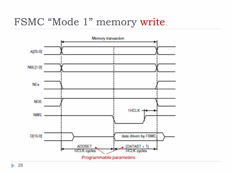
FSMC “Mode 1” memory write
28
Programmable parameters
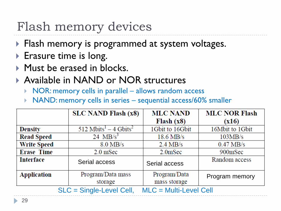
Flash memory devices Flash memory is programmed at system voltages. Erasure time is long. Must be erased in blocks. Available in NAND or NOR structures NOR: memory cells in parallel – allows random access NAND: memory cells in series – sequential access/60% smaller
29
SLC = Single-Level Cell, MLC = Multi-Level Cell
Serial access Serial access
Program memory

30
NAND and NOR flashcomparision
NAND flash similar toa hard disk drive(sequential access to bitsof a sector)
NOR flash similar to a Random-access memory(ROM/RAM)

SST39VF1601- 1M x 16 NOR Flash (on uCdragon board)
31
Similar to SRAM connection

SST39VF1601 characteristics
Organized as 1M x 16 2K word sectors, 32K word blocks
Performance: Read access time = 70ns or 90ns Word program time = 7us Sector/block erase time = 18ms Chip erase time = 40ms
Check status of write/erase operation via read DQ7 = complement of written value until write complete DQ7=0 during erase, DQ7=1 when erase done
32

SST39VF1601 read cycle timing
33
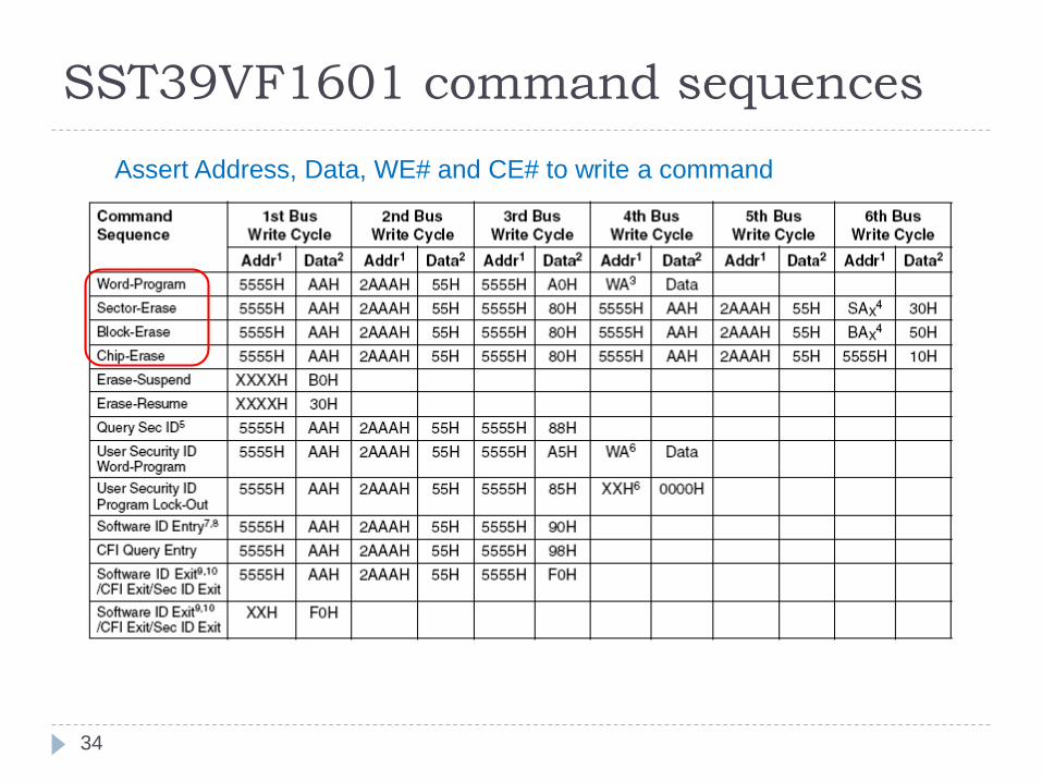
SST39VF1601 command sequences
34
Assert Address, Data, WE# and CE# to write a command

SST39VF1601 word program
TBP = 10μs max
35
1st buswrite cycle
2nd buswrite cycle
3rd buswrite cycle
4th buswrite cycle
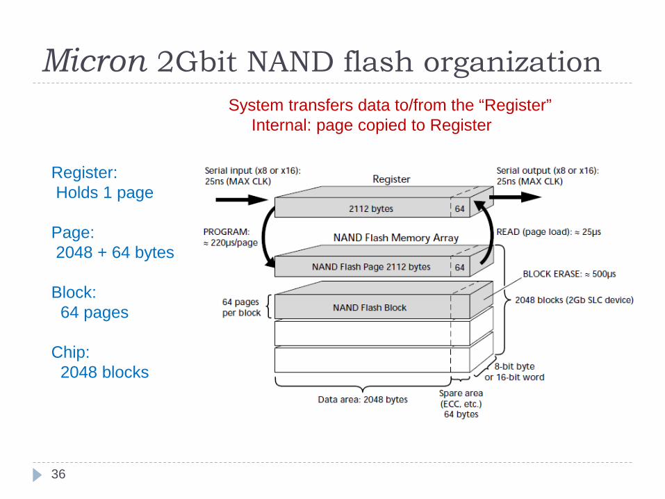
Micron 2Gbit NAND flash organization
36
Register:Holds 1 page
Page:2048 + 64 bytes
Block:64 pages
Chip:2048 blocks
System transfers data to/from the “Register”Internal: page copied to Register

NAND flash functional block diagram
37
Micron: 2/4/8 Gbit, x8/x16 multiplexed NAND flash
Bytes/wordssent/receivedsequentially

Micron Flash Mode Selection
38
CLE = command latch enable; ALE = address latch enable

Micron Flash Command Set
39

Micron NAND Flash Page Read Operation
40
Page toregister
Capacity-dependent
25 µs
Fiveaddress
cycles

Micron NAND Flash: Program & Erase Op’s
41
Program (data written to register)
Erase selected blockData sequence
3 ms
300-700 µs

Generic DRAM device
DRAM
CE#
R/W#
Address
Data
RAS#
CAS#
42
RAS# = Row Address Strobe: row# on Address inputsCAS# = Column Address Strobe: column# on Address inputs
CLKSDRAM:

Asynchronous DRAM timing
time
CE’
R/W’
RAS’
CAS’
Adrs
Data
rowadrs
coladrs
data
43

Asynchronous DRAM page mode access
time
CE’
R/W’
RAS’
CAS’
Adrs
Data
rowadrs
coladrs
data
coladrs
coladrs
data data
44

SDRAM burst read (burst length 4)
45
Trcd = RAS-to-CAS delayCL = CAS latency (CAS to data ready)Tac = access time

Dynamic RAM refresh Value decays in approx. 1 ms. Refresh value by reading it. Can’t access memory during refresh.
RAS-only refresh CAS-before-RAS refresh. Hidden refresh.
46
Example: 4 Mbyte DRAM Refreshed every 4 msec (one row at a time)Organized as 2048 rows x 2048 columns 2048 refreshesAssume 1 refresh 80 nsec
4.1% of time spent refreshing041.0104
108020483
9
≅×
××−
−
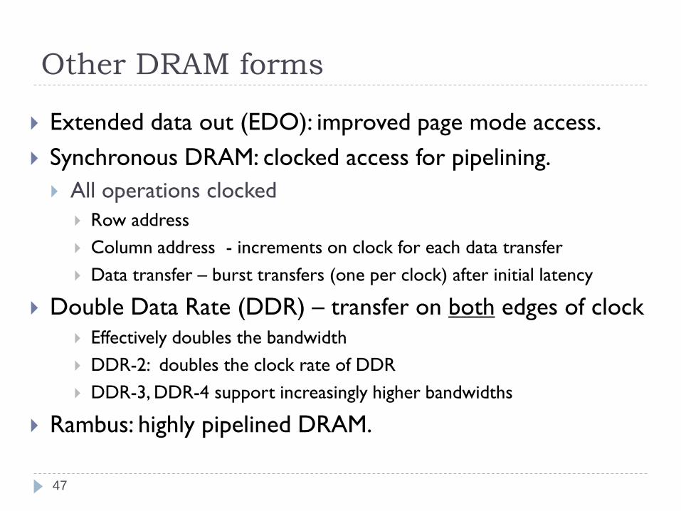
Other DRAM forms
Extended data out (EDO): improved page mode access. Synchronous DRAM: clocked access for pipelining. All operations clocked
Row address Column address - increments on clock for each data transfer Data transfer – burst transfers (one per clock) after initial latency
Double Data Rate (DDR) – transfer on both edges of clock Effectively doubles the bandwidth DDR-2: doubles the clock rate of DDR DDR-3, DDR-4 support increasingly higher bandwidths
Rambus: highly pipelined DRAM.
47

DDR2 bank activate
48
Memory partitioned into 8 separate arrays called “banks”Bank Activate command = CS# low, RAS# low, CAS# high, WE# high (and CKE high)
- Bank address BA2-BA0 selects bank- Row address A15-A0 selects a row in the bank
Follow with read/write command in next clock cycleConcurrent Bank Activate commands permitted (up to 8)

DDR2 burst read (burst length 4)
49
Burst read command = CS# low, CAS# low, RAS# high, WE# high (and CKE high)Read Latency RL = AL + CL
CL (programmable) = CAS latency (CAS to data ready)AL (programmable) = “Additive” Latency
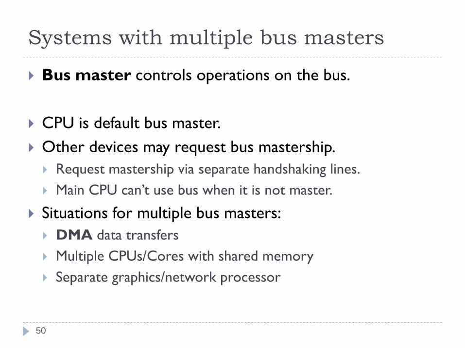
Systems with multiple bus masters
Bus master controls operations on the bus.
CPU is default bus master. Other devices may request bus mastership. Request mastership via separate handshaking lines. Main CPU can’t use bus when it is not master.
Situations for multiple bus masters: DMA data transfers Multiple CPUs/Cores with shared memory Separate graphics/network processor
50
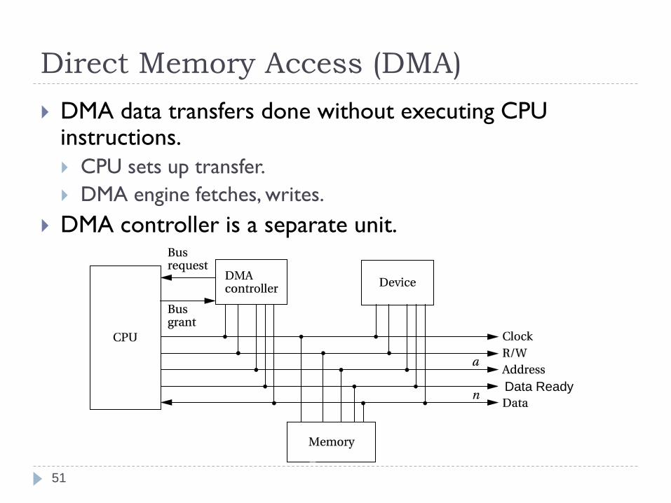
Direct Memory Access (DMA) DMA data transfers done without executing CPU
instructions. CPU sets up transfer. DMA engine fetches, writes.
DMA controller is a separate unit.
51
Data Ready

DMA operation CPU sets DMA registers for start address, length. DMA status register controls the unit. Bus request to CPU – Bus grant back from CPU
DMA controller requests bus mastership from CPU Once DMA is bus master, it transfers automatically. May run continuously until complete. May use every nth bus cycle.
52
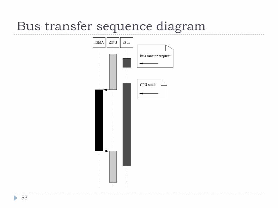
Bus transfer sequence diagram
53
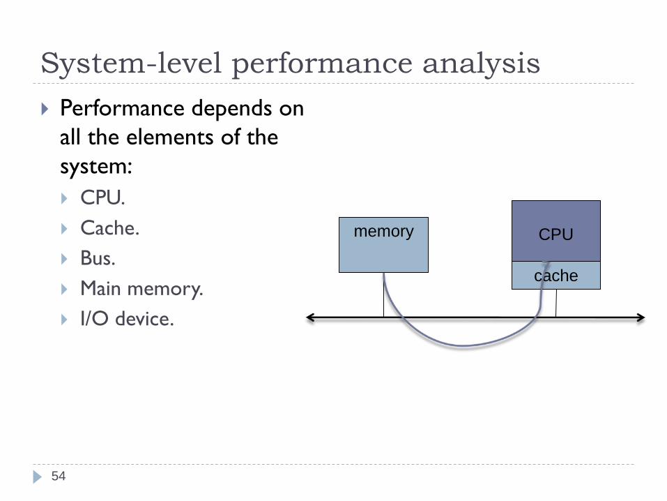
System-level performance analysis Performance depends on
all the elements of the system: CPU. Cache. Bus. Main memory. I/O device.
memory CPU
cache
54

Bandwidth as performance Bandwidth applies to several components: Memory. Bus. CPU fetches.
Different parts of the system run at different clock rates. Components may have different widths (bus, memory).
55

Bandwidth and data transfers Video frame: 320 x 240 x 3 = 230,400 bytes. Need to transfer in 1/30 sec = 0.033 sec
Transfer 1 byte/µsec, 0.23 sec per frame. Too slow.
To increase bandwidth: Increase bus width. Increase bus clock rate. Minimize overhead (do burst transfers)
56

Bus bandwidth T: # bus cycles. P: bus clock period. Total time for transfer: t = TP.
D: data payload length. O = O1 + O2 = overhead.
(before & after data)
N = total # data payloads. W = bus width (bits/xfer)
O1 D O2
W
Tbasic(N) = (D+O)N/W
57
Transfer ND bits

Bus burst transfer bandwidth T: # bus cycles. P: time/bus cycle. Total time for transfer: t = TP.
D: data payload length. B: burst size
(#transfers of size D)
O1 + O2 = overhead O. N = total # data payloads
B O
W
Tburst(N) = (BD+O)*N/(BW)
21
…
58

Bus performance bottlenecks Transfer 320 x 240 video
frame @ 30 frames/sec = 612,000 bytes/sec.
Is performance bottleneck bus or memory?
memory CPU
59
Bus: assume 1 MHz bus, D=1, O=3: Tbasic = (1+3)612,000/2 = 1,224,000 cycles = 1.224 sec.
Memory: try burst mode B=4, width w=0.5. Tmem = (4*1+4)612,000/(4*0.5) = 2,448,000 cycles = 0.2448 sec.
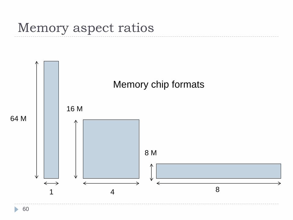
Memory aspect ratios
64 M16 M
8 M
1 4 8
60
Memory chip formats

Parallelism Speed things up by
running several units at once.
DMA provides parallelism if CPU doesn’t need the bus: DMA + bus. CPU.
61

Electrical bus design Bus signals are usually tri-stated. Address and data lines may be multiplexed. Every device on the bus must be able to drive the
maximum bus load: Bus wires. Other bus devices. Resistive and capacitive loads. Bus specification may limit loads
Bus may include clock signal. Timing is relative to clock.
62
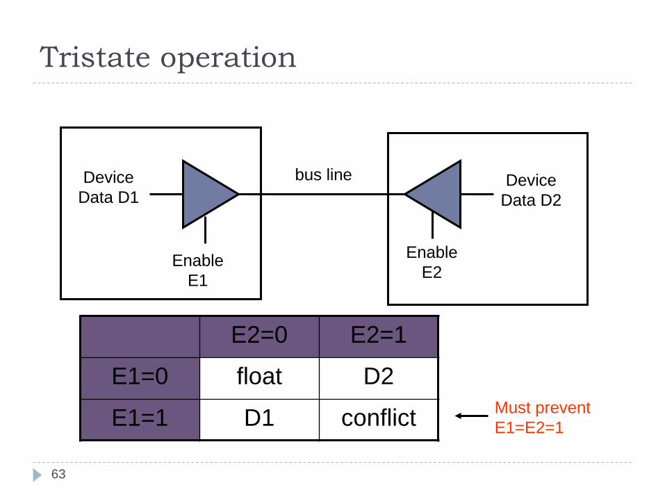
Tristate operation
E2=0 E2=1
E1=0 float D2
E1=1 D1 conflict
DeviceData D1
DeviceData D2
bus line
EnableE1
EnableE2
Must preventE1=E2=1
63


