Op-Amp Circuits: Part 1
M. B. [email protected]
www.ee.iitb.ac.in/~sequel
Department of Electrical EngineeringIndian Institute of Technology Bombay
M. B. Patil, IIT Bombay
Op-amps: introduction
* The Operational Amplifier (Op-Amp) is a versatile building block that can beused for realizing several electronic circuits.
* The characteristics of an op-amp are nearly ideal → op-amp circuits can beexpected to perform as per theoretical design in most cases.
* Amplifiers built with op-amps work with DC input voltages as well → useful insensor applications (e.g., temperature, pressure)
* The user can generally carry out circuit design without a thorough knowledgeof the intricate details of an op-amp. This makes the design process simple.
M. B. Patil, IIT Bombay
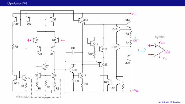
Op-Amp 741
Q23
Q2Q1
Q3 Q4
Q5 Q6
Q7
Q8
Q9
Q10
Q11
Q12
Q13 Q14
Q15
Q16
Q17
Q18
Q19
Q20
Q21
Q22
Q24R1 R2R3
R4
R6
R7
R8
R9
R10
R5CC
Symbol
offset adjust
OUT
OUT
−VEE
VCC
VCC
−VEE
M. B. Patil, IIT Bombay

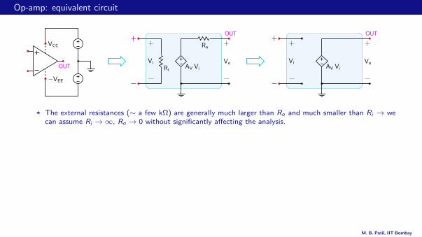
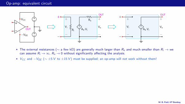
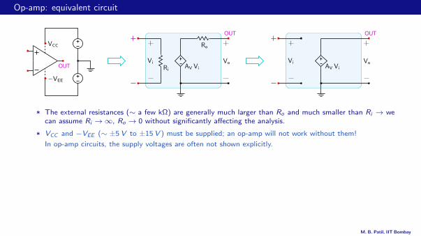
Op-amp: equivalent circuit
OUT
OUT OUT
Vo VoVi ViAV Vi AV Vi
Ro
−VEE
VCC
Ri
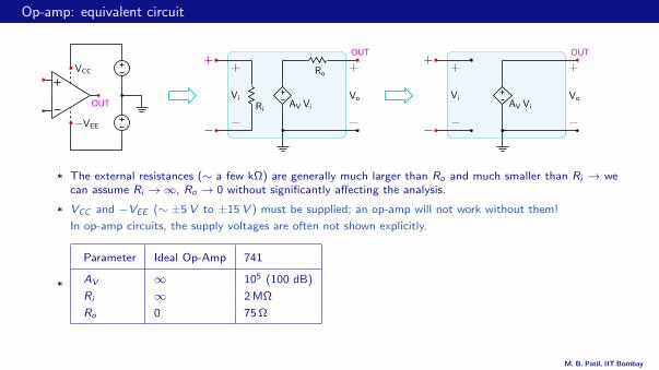
* The external resistances (∼ a few kΩ) are generally much larger than Ro and much smaller than Ri → wecan assume Ri →∞, Ro → 0 without significantly affecting the analysis.
* VCC and −VEE (∼ ±5V to ±15V ) must be supplied; an op-amp will not work without them!
In op-amp circuits, the supply voltages are often not shown explicitly.
*
Parameter Ideal Op-Amp 741
AV ∞ 105 (100 dB)
Ri ∞ 2 MΩ
Ro 0 75 Ω
M. B. Patil, IIT Bombay
Op-amp: equivalent circuit
OUT
OUT OUT
Vo VoVi ViAV Vi AV Vi
Ro
−VEE
VCC
Ri
* The external resistances (∼ a few kΩ) are generally much larger than Ro and much smaller than Ri → wecan assume Ri →∞, Ro → 0 without significantly affecting the analysis.
* VCC and −VEE (∼ ±5V to ±15V ) must be supplied; an op-amp will not work without them!
In op-amp circuits, the supply voltages are often not shown explicitly.
*
Parameter Ideal Op-Amp 741
AV ∞ 105 (100 dB)
Ri ∞ 2 MΩ
Ro 0 75 Ω
M. B. Patil, IIT Bombay

Op-Amp: equivalent circuit
linearsaturation saturation
10
5
0
−5
−10 −10
0
5
−5
10
OUT
OUTOUT
saturation
linear
saturation
0−5 5−0.2 −0.1 0 0.1 0.2
Vo VoVi ViAV Vi AV Vi
Ro
−VEE
VCC
Ri
−Vsat
Vsat
slope=AV
Vi (V)
Vo(V
)
Vo(V
)
Vi (mV)
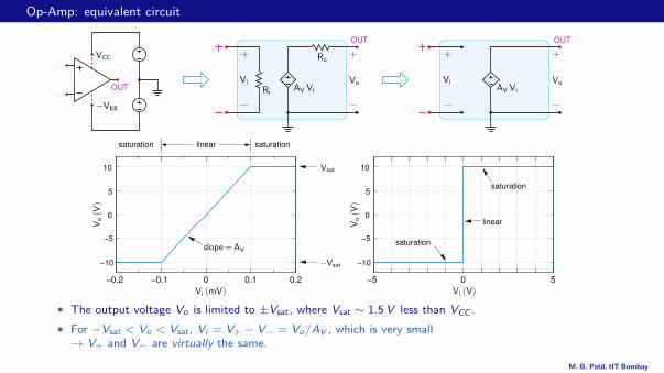
* The output voltage Vo is limited to ±Vsat, where Vsat ∼ 1.5V less than VCC .
* For −Vsat < Vo < Vsat, Vi = V+ − V− = Vo/AV , which is very small→ V+ and V− are virtually the same.
M. B. Patil, IIT Bombay

Op-Amp: equivalent circuit
linearsaturation saturation
10
5
0
−5
−10 −10
0
5
−5
10
OUT
OUTOUT
saturation
linear
saturation
0−5 5−0.2 −0.1 0 0.1 0.2
Vo VoVi ViAV Vi AV Vi
Ro
−VEE
VCC
Ri
−Vsat
Vsat
slope=AV
Vi (V)
Vo(V
)
Vo(V
)
Vi (mV)
* The output voltage Vo is limited to ±Vsat, where Vsat ∼ 1.5V less than VCC .
* For −Vsat < Vo < Vsat, Vi = V+ − V− = Vo/AV , which is very small→ V+ and V− are virtually the same.
M. B. Patil, IIT Bombay
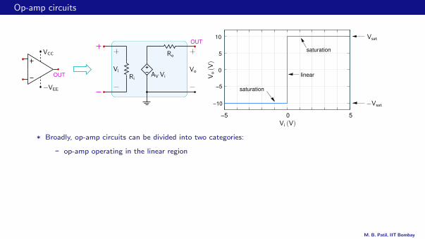
Op-amp circuits
10
−10
−5
5saturation
linear
saturation
0OUT
OUT
0−5 5
VoViAV Vi
Ro
−VEE
VCC
Ri
Vsat
−Vsat
Vi (V)
Vo(V
)
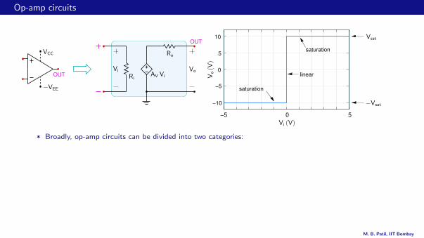
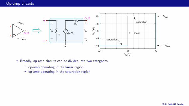
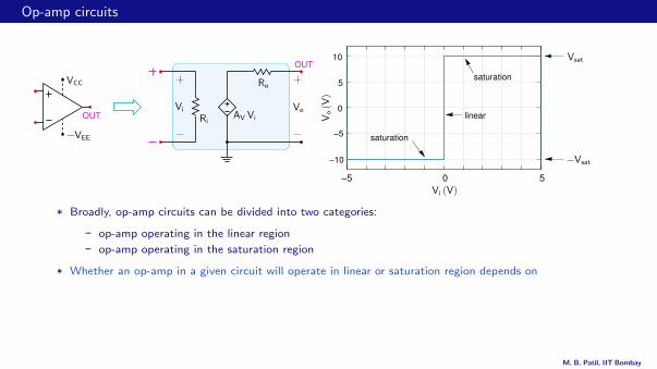
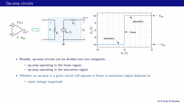
* Broadly, op-amp circuits can be divided into two categories:
- op-amp operating in the linear region
- op-amp operating in the saturation region
* Whether an op-amp in a given circuit will operate in linear or saturation region depends on
- input voltage magnitude
- type of feedback (negative or positive)
(We will take a qualitative look at feedback later.)
M. B. Patil, IIT Bombay
Op-amp circuits
10
−10
−5
5saturation
linear
saturation
0OUT
OUT
0−5 5
VoViAV Vi
Ro
−VEE
VCC
Ri
Vsat
−Vsat
Vi (V)
Vo(V
)
* Broadly, op-amp circuits can be divided into two categories:
- op-amp operating in the linear region
- op-amp operating in the saturation region
* Whether an op-amp in a given circuit will operate in linear or saturation region depends on
- input voltage magnitude
- type of feedback (negative or positive)
(We will take a qualitative look at feedback later.)
M. B. Patil, IIT Bombay
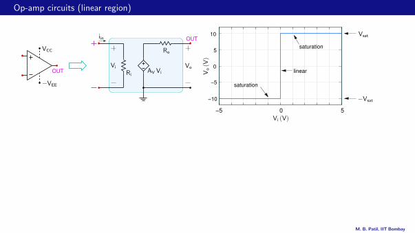
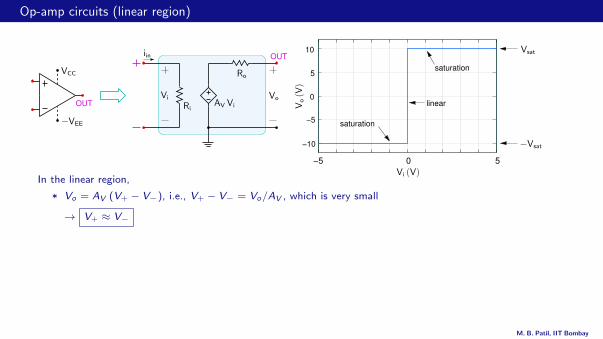
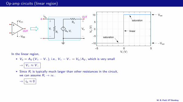
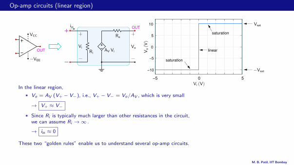
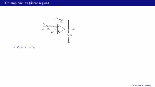
Op-amp circuits (linear region)
10
−10
−5
5saturation
linear
saturation
0OUT
OUT
0−5 5
VoViAV Vi
Ro
−VEE
VCC
Ri
iinVsat
−Vsat
Vi (V)
Vo(V
)
In the linear region,
* Vo = AV (V+ − V−), i.e., V+ − V− = Vo/AV , which is very small
→ V+ ≈ V−
* Since Ri is typically much larger than other resistances in the circuit,we can assume Ri →∞ .
→ iin ≈ 0
These two “golden rules” enable us to understand several op-amp circuits.
M. B. Patil, IIT Bombay
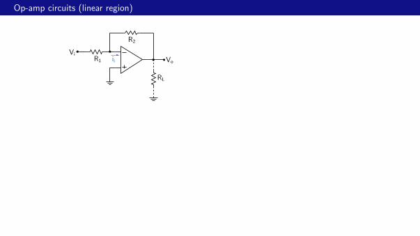
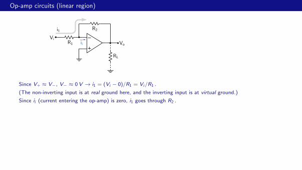
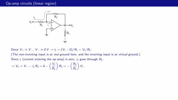
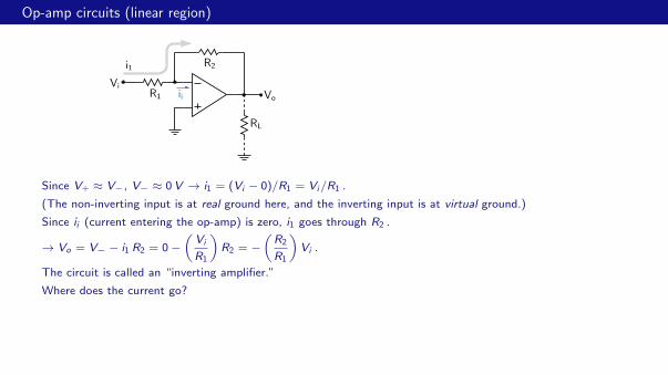
Op-amp circuits (linear region)
ii
RL
R2
R1
Vi
Vo
i1
RL
R2
R1
i1
Vi
Vo0.1 V−1V
Since V+ ≈ V−, V− ≈ 0V → i1 = (Vi − 0)/R1 = Vi/R1 .
(The non-inverting input is at real ground here, and the inverting input is at virtual ground.)
Since ii (current entering the op-amp) is zero, i1 goes through R2 .
→ Vo = V− − i1 R2 = 0−(Vi
R1
)R2 = −
(R2
R1
)Vi .
The circuit is called an “inverting amplifier.”
Where does the current go?
(Op-amp 741 can source or sink about 25 mA.)
M. B. Patil, IIT Bombay
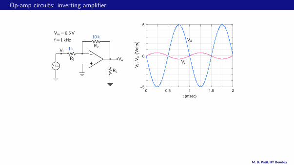
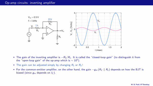
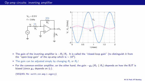
Op-amp circuits: inverting amplifier
5
0
−5 0 0.5 1 1.5 2
t (msec)
RL
R2
R1
Vi
Vm =0.5V
f=1 kHz
Vo
10 k
1 k
Vi
Vi,V
o(Volts) Vo
* The gain of the inverting amplifier is −R2/R1. It is called the “closed-loop gain” (to distinguish it fromthe “open-loop gain” of the op-amp which is ∼ 105).
* The gain can be adjusted simply by changing R1 or R2 !
* For the common-emitter amplifier, on the other hand, the gain −gm (RC ‖ RL) depends on how the BJT isbiased (since gm depends on IC ).
(SEQUEL file: ee101 inv amp 1.sqproj)
M. B. Patil, IIT Bombay
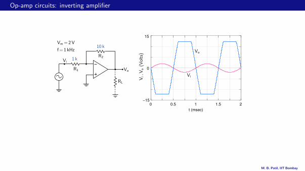
Op-amp circuits: inverting amplifier
15
0
−15 0 0.5 1 1.5 2
t (msec)
RL
R2
R1
Vi
Vm =2V
f=1 kHz
Vo
10 k
1 k
Vo
Vi
Vi,V
o(Volts)
* The output voltage is limited to ±Vsat.
* Vsat is ∼ 1.5 V less than the supply voltage VCC .
M. B. Patil, IIT Bombay

Op-amp circuits: inverting amplifier
15
0
−15 0 0.5 1 1.5 2
t (msec)
RL
R2
R1
Vi
Vm =2V
f=1 kHz
Vo
10 k
1 k
Vo
Vi
Vi,V
o(Volts)
* The output voltage is limited to ±Vsat.
* Vsat is ∼ 1.5 V less than the supply voltage VCC .
M. B. Patil, IIT Bombay

Op-amp circuits: inverting amplifier
15
0
−15 0 0.5 1 1.5 2
t (msec)
RL
R2
R1
Vi
Vm =2V
f=1 kHz
Vo
10 k
1 k
Vo
Vi
Vi,V
o(Volts)
* The output voltage is limited to ±Vsat.
* Vsat is ∼ 1.5 V less than the supply voltage VCC .
M. B. Patil, IIT Bombay
Op-amp circuits: inverting amplifier
10
0 20 40 60 80
0
−10
RL
R2
R1
Vi
Vm=1V
f=25 kHz
Vo
10 k
1 k
Vi,V
o(Volts)
Vo (expected)
Vo
Vi
t (µsec)
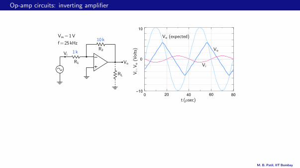
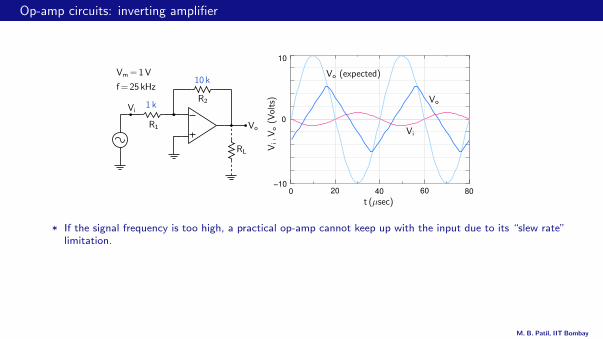
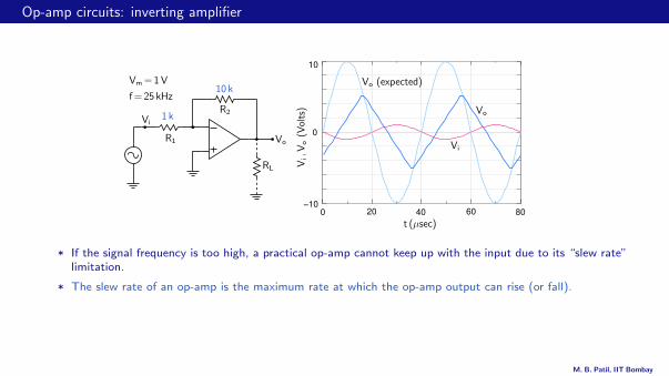
* If the signal frequency is too high, a practical op-amp cannot keep up with the input due to its “slew rate”limitation.
* The slew rate of an op-amp is the maximum rate at which the op-amp output can rise (or fall).
* For the 741, the slew rate is 0.5V /µsec.
(SEQUEL file: ee101 inv amp 2.sqproj)
M. B. Patil, IIT Bombay
Op-amp circuits: inverting amplifier
10
0 20 40 60 80
0
−10
RL
R2
R1
Vi
Vm=1V
f=25 kHz
Vo
10 k
1 k
Vi,V
o(Volts)
Vo (expected)
Vo
Vi
t (µsec)
* If the signal frequency is too high, a practical op-amp cannot keep up with the input due to its “slew rate”limitation.
* The slew rate of an op-amp is the maximum rate at which the op-amp output can rise (or fall).
* For the 741, the slew rate is 0.5V /µsec.
(SEQUEL file: ee101 inv amp 2.sqproj)
M. B. Patil, IIT Bombay
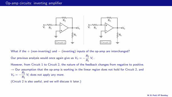
Op-amp circuits: inverting amplifier
RLRL
R2R2
R1R1ViVi VoVo
Circuit 1 Circuit 2
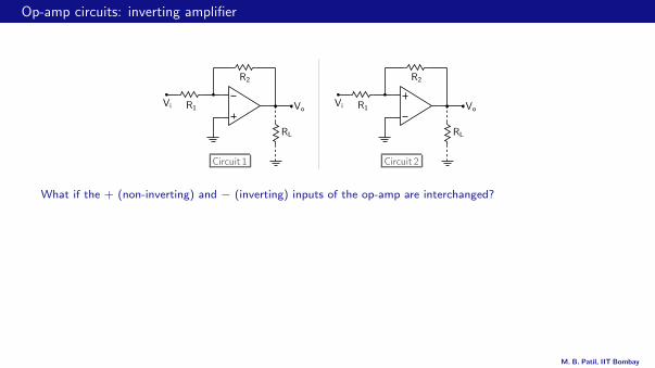
What if the + (non-inverting) and − (inverting) inputs of the op-amp are interchanged?
Our previous analysis would once again give us Vo = −R2
R1Vi .
However, from Circuit 1 to Circuit 2, the nature of the feedback changes from negative to positive.
→ Our assumption that the op-amp is working in the linear region does not hold for Circuit 2, and
Vo = −R2
R1Vi does not apply any more.
(Circuit 2 is also useful, and we will discuss it later.)
M. B. Patil, IIT Bombay

Op-amp circuits: inverting amplifier
RLRL
R2R2
R1R1ViVi VoVo
Circuit 1 Circuit 2
What if the + (non-inverting) and − (inverting) inputs of the op-amp are interchanged?
Our previous analysis would once again give us Vo = −R2
R1Vi .
However, from Circuit 1 to Circuit 2, the nature of the feedback changes from negative to positive.
→ Our assumption that the op-amp is working in the linear region does not hold for Circuit 2, and
Vo = −R2
R1Vi does not apply any more.
(Circuit 2 is also useful, and we will discuss it later.)
M. B. Patil, IIT Bombay
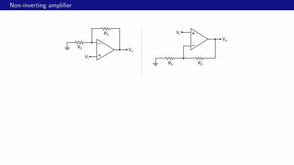
Op-amp circuits (linear region)
ii
i1
i2
RL
R2
R1
Vi
Vo
* V+ ≈ V− = Vi
→ i1 = (0− Vi )/R1 = −Vi/R1 .
* Since ii = 0, i2 = i1 → Vo = V− − i2 R2 = V+ − i1 R2 = Vi −(−Vi
R1
)R2 = Vi
(1 +
R2
R1
).
* This circuit is known as the “non-inverting amplifier.”
* Again, interchanging + and − changes the nature of the feedback from negative to positive, and thecircuit operation becomes completely different.
M. B. Patil, IIT Bombay

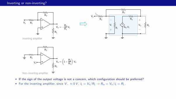
Inverting or non-inverting?
Inverting amplifier
Non−inverting amplifier
RL
RL
R2
R2
R1
R1
Vs
Vs
Vo = −R2
R1Vs
Vo =
(1+
R2
R1
)Vs
i1Vs
RL
R1
R2
VoViAV Vi
Ro
Ri
Vs
RL
R1
R2
VoViAV Vi
Ro
Ri
* If the sign of the output voltage is not a concern, which configuration should be preferred?
* For the inverting amplifier, since V− ≈ 0V , i1 = Vs/R1 → Rin = Vs/i1 = R1 .
* For the non-inverting amplifier, Rin ∼ Ri AVR1
R1 + R2. Huge!
M. B. Patil, IIT Bombay

Inverting and non-inverting amplifiers: summary
Inverting amplifier Non−inverting amplifier
RL RL
R2 R2
R1 R1Vs
Vs
Vo = −R2
R1Vs Vo =
(1+
R2
R1
)Vs
M. B. Patil, IIT Bombay
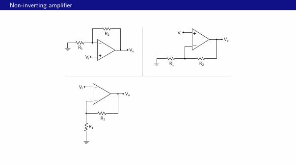
Non-inverting amplifier
R2
R1
Vi
Vo
R2R1
Vi
Vo
R2
R1
Vi
Vo
R1
R2
Vi
Vo
M. B. Patil, IIT Bombay
Non-inverting amplifier
R2
R1
Vi
Vo
R2R1
Vi
Vo
R2
R1
Vi
Vo
R1
R2
Vi
Vo
M. B. Patil, IIT Bombay
Non-inverting amplifier
R2
R1
Vi
Vo
R2R1
Vi
Vo
R2
R1
Vi
Vo
R1
R2
Vi
Vo
M. B. Patil, IIT Bombay

Non-inverting amplifier
R2
R1
Vi
Vo
R2R1
Vi
Vo
R2
R1
Vi
Vo
R1
R2
Vi
Vo
M. B. Patil, IIT Bombay
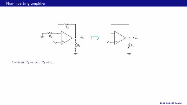
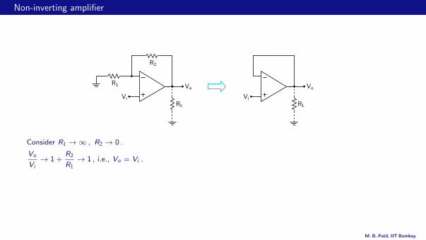
Non-inverting amplifier
RL RL
R2
R1 Vo Vo
Vi Vi
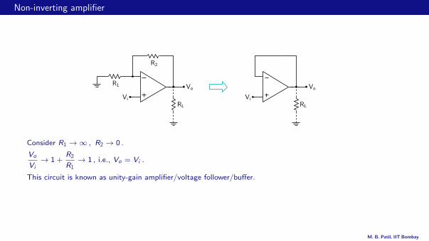
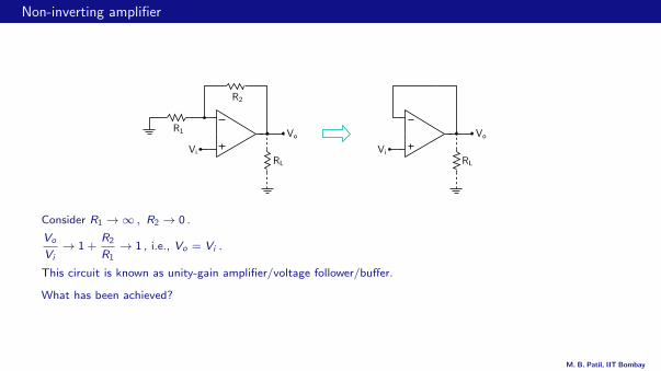
Consider R1 →∞ , R2 → 0 .
Vo
Vi→ 1 +
R2
R1→ 1 , i.e., Vo = Vi .
This circuit is known as unity-gain amplifier/voltage follower/buffer.
What has been achieved?
M. B. Patil, IIT Bombay
Non-inverting amplifier
RL RL
R2
R1 Vo Vo
Vi Vi
Consider R1 →∞ , R2 → 0 .
Vo
Vi→ 1 +
R2
R1→ 1 , i.e., Vo = Vi .
This circuit is known as unity-gain amplifier/voltage follower/buffer.
What has been achieved?
M. B. Patil, IIT Bombay
Non-inverting amplifier
RL RL
R2
R1 Vo Vo
Vi Vi
Consider R1 →∞ , R2 → 0 .
Vo
Vi→ 1 +
R2
R1→ 1 , i.e., Vo = Vi .
This circuit is known as unity-gain amplifier/voltage follower/buffer.
What has been achieved?
M. B. Patil, IIT Bombay
Non-inverting amplifier
RL RL
R2
R1 Vo Vo
Vi Vi
Consider R1 →∞ , R2 → 0 .
Vo
Vi→ 1 +
R2
R1→ 1 , i.e., Vo = Vi .
This circuit is known as unity-gain amplifier/voltage follower/buffer.
What has been achieved?
M. B. Patil, IIT Bombay

Loading effects
Vs RL
Rs
Vi VoAV Vi
Ro
Ri
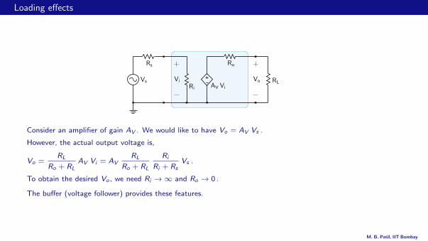
Consider an amplifier of gain AV . We would like to have Vo = AV Vs .
However, the actual output voltage is,
Vo =RL
Ro + RLAV Vi = AV
RL
Ro + RL
Ri
Ri + RsVs .
To obtain the desired Vo , we need Ri →∞ and Ro → 0 .
The buffer (voltage follower) provides these features.
M. B. Patil, IIT Bombay

Loading effects
Vs RL
Rs
Vi VoAV Vi
Ro
Ri
Consider an amplifier of gain AV . We would like to have Vo = AV Vs .
However, the actual output voltage is,
Vo =RL
Ro + RLAV Vi = AV
RL
Ro + RL
Ri
Ri + RsVs .
To obtain the desired Vo , we need Ri →∞ and Ro → 0 .
The buffer (voltage follower) provides these features.
M. B. Patil, IIT Bombay
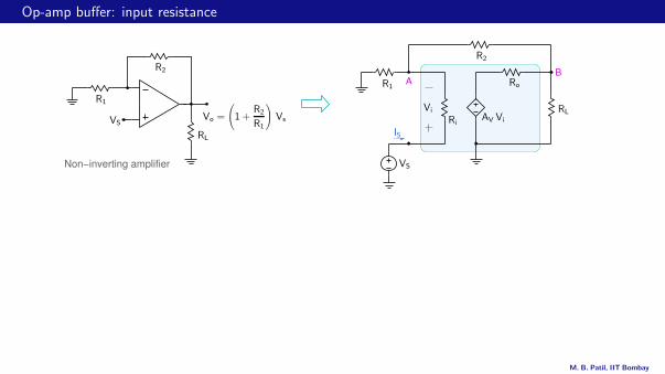
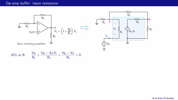
Op-amp buffer: input resistance
Non−inverting amplifier
AB
ISRL
R2
R1
VS
RL
R1
R2
VS
ViAV Vi
Ro
RiVo =
(1+
R2
R1
)Vs
KCL at B:VB
RL+
VB − AVVi
Ro+
VB − VA
R2= 0.
Source current: IS =VA
R1+
VA − VB
R2.
Using Vi = ISRi , VA =VS − Vi , and after some algebra, we get
Rin =VS
IS=
(1 +
Ro
RL+
Ro
R2
)+ Ri
[(1
R1+
1
R2
)(1 +
Ro
RL+
Ro
R2
)− Ro
R22
+AV
R2
](
1
R1+
1
R2
)(1 +
Ro
RL+
Ro
R2
)− Ro
R22
. STOP
M. B. Patil, IIT Bombay

Op-amp buffer: input resistance
Non−inverting amplifier
AB
ISRL
R2
R1
VS
RL
R1
R2
VS
ViAV Vi
Ro
RiVo =
(1+
R2
R1
)Vs
KCL at B:VB
RL+
VB − AVVi
Ro+
VB − VA
R2= 0.
Source current: IS =VA
R1+
VA − VB
R2.
Using Vi = ISRi , VA =VS − Vi , and after some algebra, we get
Rin =VS
IS=
(1 +
Ro
RL+
Ro
R2
)+ Ri
[(1
R1+
1
R2
)(1 +
Ro
RL+
Ro
R2
)− Ro
R22
+AV
R2
](
1
R1+
1
R2
)(1 +
Ro
RL+
Ro
R2
)− Ro
R22
.
STOP
M. B. Patil, IIT Bombay
Op-amp buffer: input resistance
Non−inverting amplifier
AB
ISRL
R2
R1
VS
RL
R1
R2
VS
ViAV Vi
Ro
RiVo =
(1+
R2
R1
)Vs
KCL at B:VB
RL+
VB − AVVi
Ro+
VB − VA
R2= 0.
Source current: IS =VA
R1+
VA − VB
R2.
Using Vi = ISRi , VA =VS − Vi , and after some algebra, we get
Rin =VS
IS=
(1 +
Ro
RL+
Ro
R2
)+ Ri
[(1
R1+
1
R2
)(1 +
Ro
RL+
Ro
R2
)− Ro
R22
+AV
R2
](
1
R1+
1
R2
)(1 +
Ro
RL+
Ro
R2
)− Ro
R22
. STOP
M. B. Patil, IIT Bombay

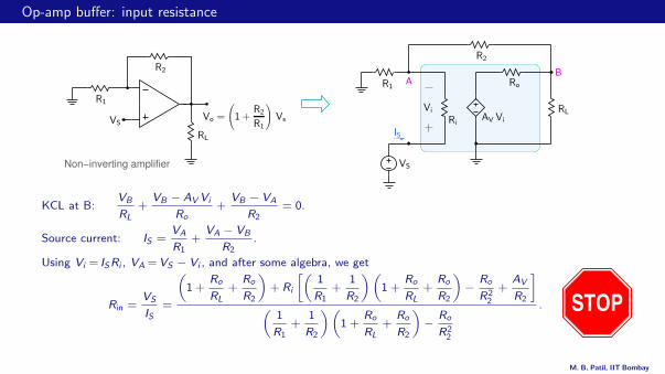
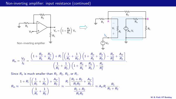
Non-inverting amplifier: input resistance (continued)
Non−inverting amplifier
AB
ISRL
R2
R1
VS
RL
R1
R2
VS
ViAV Vi
Ro
RiVo =
(1+
R2
R1
)Vs
Rin =VS
IS=
(1 +
Ro
RL+
Ro
R2
)+ Ri
[(1
R1+
1
R2
)(1 +
Ro
RL+
Ro
R2
)− Ro
R22
+AV
R2
](
1
R1+
1
R2
)(1 +
Ro
RL+
Ro
R2
)− Ro
R22
.
Since Ro is much smaller than R1, R2, RL, or Ri ,
Rin ≈1 + Ri
[(1
R1+
1
R2
)+
AV
R2
](
1
R1+
1
R2
) ≈Ri
[R1 + R2
R1R2+
AV
R2
]R1 + R2
R1R2
≈ AVRiR1
R1 + R2.
M. B. Patil, IIT Bombay
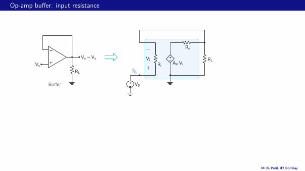
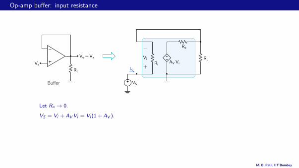
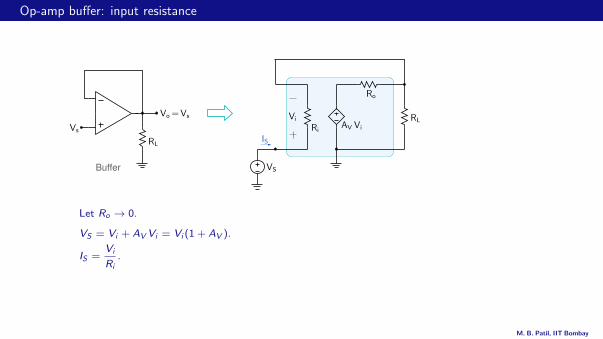
Op-amp buffer: input resistance
Buffer
ISRL
VS
RL
Vs
ViAV Vi
Ro
Ri
Vo=Vs
Let Ro → 0.
VS = Vi + AVVi = Vi (1 + AV ).
IS =Vi
Ri.
→ Rin =VS
IS= Ri (AV + 1)
M. B. Patil, IIT Bombay

Op-amp buffer: input resistance
Buffer
ISRL
VS
RL
Vs
ViAV Vi
Ro
Ri
Vo=Vs
Let Ro → 0.
VS = Vi + AVVi = Vi (1 + AV ).
IS =Vi
Ri.
→ Rin =VS
IS= Ri (AV + 1)
M. B. Patil, IIT Bombay
Op-amp buffer: input resistance
Buffer
ISRL
VS
RL
Vs
ViAV Vi
Ro
Ri
Vo=Vs
Let Ro → 0.
VS = Vi + AVVi = Vi (1 + AV ).
IS =Vi
Ri.
→ Rin =VS
IS= Ri (AV + 1)
M. B. Patil, IIT Bombay
Op-amp buffer: input resistance
Buffer
ISRL
VS
RL
Vs
ViAV Vi
Ro
Ri
Vo=Vs
Let Ro → 0.
VS = Vi + AVVi = Vi (1 + AV ).
IS =Vi
Ri.
→ Rin =VS
IS= Ri (AV + 1)
M. B. Patil, IIT Bombay

Op-amp buffer: input resistance
Buffer
ISRL
VS
RL
Vs
ViAV Vi
Ro
Ri
Vo=Vs
Let Ro → 0.
VS = Vi + AVVi = Vi (1 + AV ).
IS =Vi
Ri.
→ Rin =VS
IS= Ri (AV + 1)
M. B. Patil, IIT Bombay

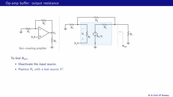
Op-amp buffer: output resistance
Non−inverting amplifier
RL
Vo
R2
R1
Vs
RL
Vs
R1
R2
ViAV Vi
Ro
Ri
Rout
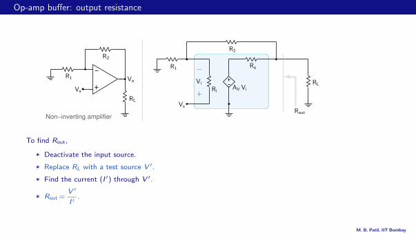
To find Rout,
* Deactivate the input source.
* Replace RL with a test source V ′.
* Find the current (I ′) through V ′.
* Rout =V ′
I ′.
M. B. Patil, IIT Bombay
Op-amp buffer: output resistance
Non−inverting amplifier
RL
Vo
R2
R1
Vs
RL
Vs
R1
R2
ViAV Vi
Ro
Ri
Rout
To find Rout,
* Deactivate the input source.
* Replace RL with a test source V ′.
* Find the current (I ′) through V ′.
* Rout =V ′
I ′.
M. B. Patil, IIT Bombay
Op-amp buffer: output resistance
Non−inverting amplifier
RL
Vo
R2
R1
Vs
RL
Vs
R1
R2
ViAV Vi
Ro
Ri
Rout
To find Rout,
* Deactivate the input source.
* Replace RL with a test source V ′.
* Find the current (I ′) through V ′.
* Rout =V ′
I ′.
M. B. Patil, IIT Bombay
Op-amp buffer: output resistance
Non−inverting amplifier
RL
Vo
R2
R1
Vs
RL
Vs
R1
R2
ViAV Vi
Ro
Ri
Rout
To find Rout,
* Deactivate the input source.
* Replace RL with a test source V ′.
* Find the current (I ′) through V ′.
* Rout =V ′
I ′.
M. B. Patil, IIT Bombay
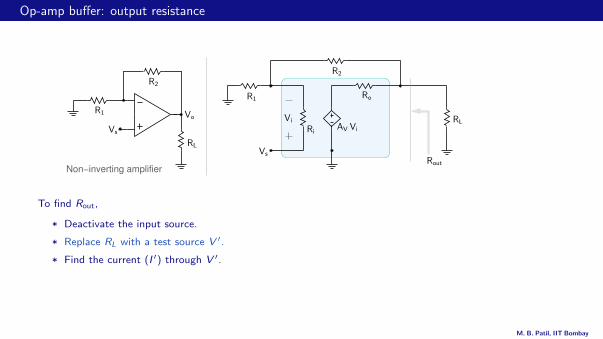
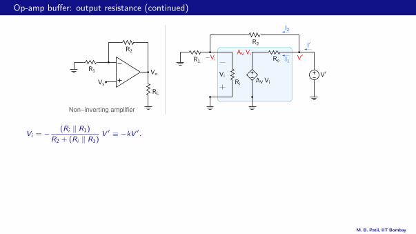
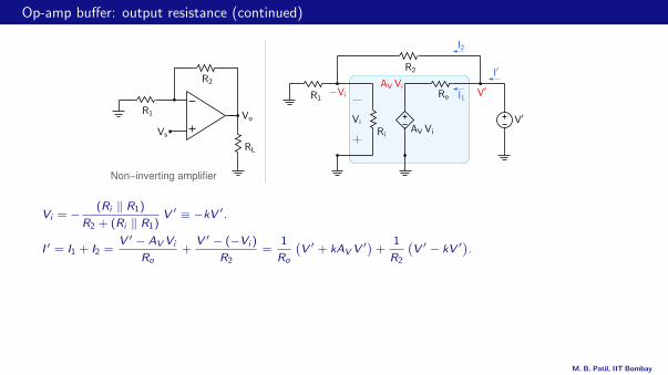
Op-amp buffer: output resistance (continued)
Non−inverting amplifier
I′
I2
I1
RL
Vo
R2
V′
V′−Vi
R1
R1
R2
Vs
ViAV Vi
Ro
Ri
AV Vi
Vi = − (Ri ‖ R1)
R2 + (Ri ‖ R1)V ′ ≡ −kV ′.
I ′ = I1 + I2 =V ′ − AVVi
Ro+
V ′ − (−Vi )
R2=
1
Ro
(V ′ + kAVV
′) +1
R2
(V ′ − kV ′
).
I ′
V ′=
1
Ro(1 + kAV ) +
1
R2(1− k)→ Rout =
V ′
I ′=
Ro
(1 + kAV )‖ R2
(1− k)≈ Ro
(1 + kAV )
Special case: Op-amp buffer
k =(Ri ‖ R1)
R2 + (Ri ‖ R1)→ 1 ⇒ Rout≈
Ro
1 + AV
M. B. Patil, IIT Bombay
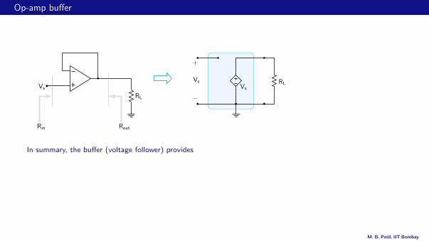
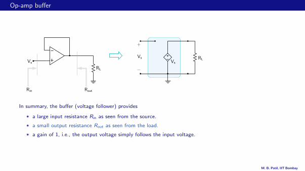
Op-amp buffer
RL
Vs RLVs Vs
Rin Rout
In summary, the buffer (voltage follower) provides
* a large input resistance Rin as seen from the source.
* a small output resistance Rout as seen from the load.
* a gain of 1, i.e., the output voltage simply follows the input voltage.
M. B. Patil, IIT Bombay

Op-amp buffer
RL
Vs RLVs Vs
Rin Rout
In summary, the buffer (voltage follower) provides
* a large input resistance Rin as seen from the source.
* a small output resistance Rout as seen from the load.
* a gain of 1, i.e., the output voltage simply follows the input voltage.
M. B. Patil, IIT Bombay

Op-amp buffer
RL
Vs RLVs Vs
Rin Rout
In summary, the buffer (voltage follower) provides
* a large input resistance Rin as seen from the source.
* a small output resistance Rout as seen from the load.
* a gain of 1, i.e., the output voltage simply follows the input voltage.
M. B. Patil, IIT Bombay
Op-amp buffer
RL
Vs RLVs Vs
Rin Rout
In summary, the buffer (voltage follower) provides
* a large input resistance Rin as seen from the source.
* a small output resistance Rout as seen from the load.
* a gain of 1, i.e., the output voltage simply follows the input voltage.
M. B. Patil, IIT Bombay
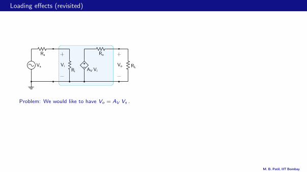
Loading effects (revisited)
Vs RL
Rs
Vi VoAV Vi
Ro
Ri
Problem: We would like to have Vo = AV Vs .
But the actual output voltage is,
Vo =RL
Ro + RLAV Vi = AV
RL
Ro + RL
Ri
Ri + RsVs .
M. B. Patil, IIT Bombay

Loading effects (revisited)
Vs RL
Rs
Vi VoAV Vi
Ro
Ri
Problem: We would like to have Vo = AV Vs .
But the actual output voltage is,
Vo =RL
Ro + RLAV Vi = AV
RL
Ro + RL
Ri
Ri + RsVs .
M. B. Patil, IIT Bombay
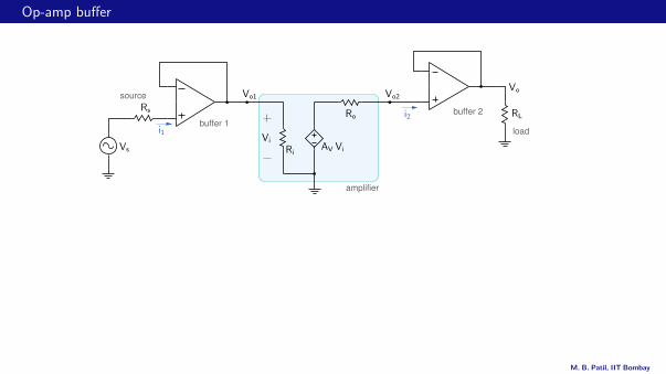
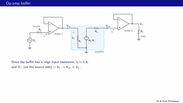
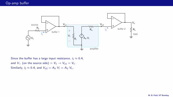
Op-amp buffer
buffer 2
load
amplifier
buffer 1
source
RL
Vs
Rs
ViAV Vi
Ro
Ri
Vo
i1
i2
Vo1 Vo2
Since the buffer has a large input resistance, i1 ≈ 0A,
and V+ (on the source side) = Vs → Vo1 = Vs .
Similarly, i2 ≈ 0A, and Vo2 = AV Vi = AV Vs .
Finally, Vo = Vo2 = AV Vs , as desired, irrespective of RS and RL.
Note that the load current is supplied by the second buffer which acts as a voltage source (=AVVs) with zerosource resistance.
M. B. Patil, IIT Bombay
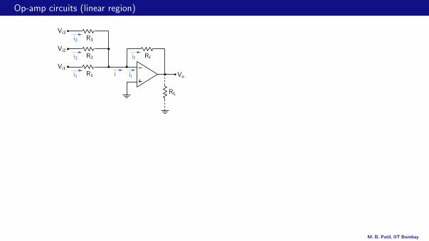
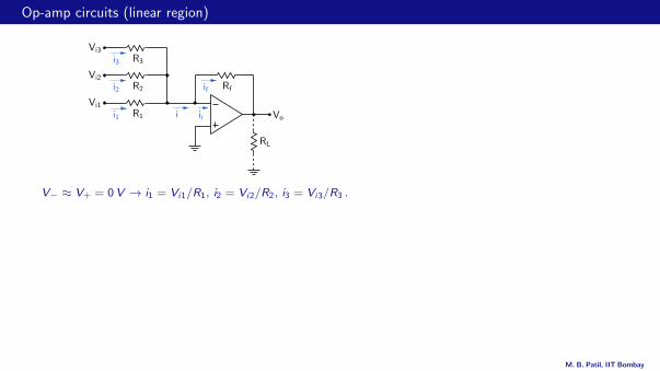
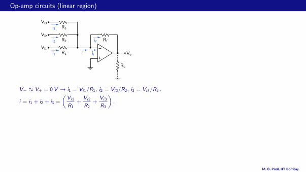
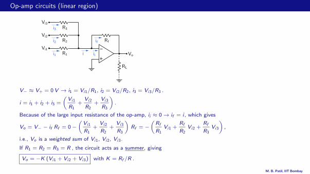
Op-amp circuits (linear region)
Vi3
Vi2
Vi1
RL
Vo
Rf
R3
R2
R1
i3
i2
i1 i ii
if
V− ≈ V+ = 0V → i1 = Vi1/R1, i2 = Vi2/R2, i3 = Vi3/R3 .
i = i1 + i2 + i3 =
(Vi1
R1+
Vi2
R2+
Vi3
R3
).
Because of the large input resistance of the op-amp, ii ≈ 0→ if = i , which gives
Vo = V− − if Rf = 0−(Vi1
R1+
Vi2
R2+
Vi3
R3
)Rf = −
(Rf
R1Vi1 +
Rf
R2Vi2 +
Rf
R3Vi3
),
i.e., Vo is a weighted sum of Vi1, Vi2, Vi3.
If R1 = R2 = R3 = R , the circuit acts as a summer, giving
Vo = −K (Vi1 + Vi2 + Vi3) with K = Rf /R .
M. B. Patil, IIT Bombay
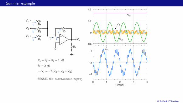
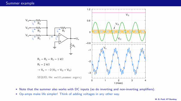
Summer example
1.2
0.6
0
−0.6
−1
−2
−3
0 1 2 3 4t (msec)
Vi3
Vi2
Vi1
RL
Vo
Rf
R3
R2
R1
SEQUEL file: ee101 summer.sqproj
R1 = R2 = R3 = 1 kΩ
Rf = 2 kΩ
→ Vo = −2 (Vi1 + Vi2 + Vi3)
i3
i2
i1 i ii
if
Vi2
Vi1
Vi3
Vo
* Note that the summer also works with DC inputs (so do inverting and non-inverting amplifiers).
* Op-amps make life simpler! Think of adding voltages in any other way.
M. B. Patil, IIT Bombay

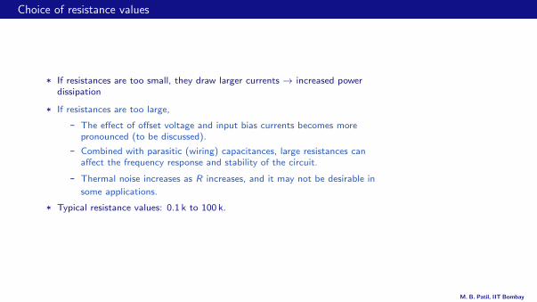
Choice of resistance values
* If resistances are too small, they draw larger currents → increased powerdissipation
* If resistances are too large,
- The effect of offset voltage and input bias currents becomes morepronounced (to be discussed).
- Combined with parasitic (wiring) capacitances, large resistances canaffect the frequency response and stability of the circuit.
- Thermal noise increases as R increases, and it may not be desirable in
some applications.
* Typical resistance values: 0.1 k to 100 k.
M. B. Patil, IIT Bombay

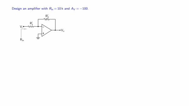
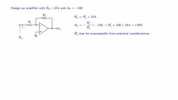
Design an amplifier with Rin = 10 k and AV =−100.
Vo
Vi
Rin
R′2
R′1
Vo
Vi
R′1
I1V10V
Rin = R′1 = 10 k.
AV = − R′2R′1
= −100→ R′2 = 100× 10 k = 1 MΩ
R′2 may be unacceptable from practical considerations.
→ need a design with smaller resistances.
If we ensureV1
I1= R′2, we will satisfy the gain condition.
M. B. Patil, IIT Bombay
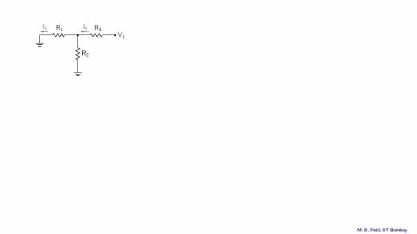
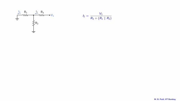
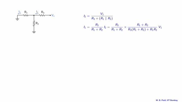
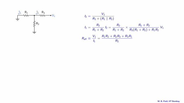
I1V1
I2R1
R2
R3
I2 =V1
R3 + (R1 ‖ R2)
I1 =R2
R1 + R2I2 =
R2
R1 + R2× R1 + R2
R3(R1 + R2) + R1R2V1
Reff ≡V1
I1=
R1R2 + R2R3 + R3R1
R2
→ Choose R1, R2, R3 such that Reff =R′2 = 1 MΩ.
Vo
Vi
R′2
Vo
Vi
R2R′1
R′1
R1 R3
M. B. Patil, IIT Bombay
I1V1
I2R1
R2
R3
I2 =V1
R3 + (R1 ‖ R2)
I1 =R2
R1 + R2I2 =
R2
R1 + R2× R1 + R2
R3(R1 + R2) + R1R2V1
Reff ≡V1
I1=
R1R2 + R2R3 + R3R1
R2
→ Choose R1, R2, R3 such that Reff =R′2 = 1 MΩ.
Vo
Vi
R′2
Vo
Vi
R2R′1
R′1
R1 R3
M. B. Patil, IIT Bombay
I1V1
I2R1
R2
R3
I2 =V1
R3 + (R1 ‖ R2)
I1 =R2
R1 + R2I2 =
R2
R1 + R2× R1 + R2
R3(R1 + R2) + R1R2V1
Reff ≡V1
I1=
R1R2 + R2R3 + R3R1
R2
→ Choose R1, R2, R3 such that Reff =R′2 = 1 MΩ.
Vo
Vi
R′2
Vo
Vi
R2R′1
R′1
R1 R3
M. B. Patil, IIT Bombay
I1V1
I2R1
R2
R3
I2 =V1
R3 + (R1 ‖ R2)
I1 =R2
R1 + R2I2 =
R2
R1 + R2× R1 + R2
R3(R1 + R2) + R1R2V1
Reff ≡V1
I1=
R1R2 + R2R3 + R3R1
R2
→ Choose R1, R2, R3 such that Reff =R′2 = 1 MΩ.
Vo
Vi
R′2
Vo
Vi
R2R′1
R′1
R1 R3
M. B. Patil, IIT Bombay

I1V1
I2R1
R2
R3
I2 =V1
R3 + (R1 ‖ R2)
I1 =R2
R1 + R2I2 =
R2
R1 + R2× R1 + R2
R3(R1 + R2) + R1R2V1
Reff ≡V1
I1=
R1R2 + R2R3 + R3R1
R2
→ Choose R1, R2, R3 such that Reff =R′2 = 1 MΩ.
Vo
Vi
R′2
Vo
Vi
R2R′1
R′1
R1 R3
M. B. Patil, IIT Bombay

I1V1
I2R1
R2
R3
I2 =V1
R3 + (R1 ‖ R2)
I1 =R2
R1 + R2I2 =
R2
R1 + R2× R1 + R2
R3(R1 + R2) + R1R2V1
Reff ≡V1
I1=
R1R2 + R2R3 + R3R1
R2
→ Choose R1, R2, R3 such that Reff =R′2 = 1 MΩ.
Vo
Vi
R′2
Vo
Vi
R2R′1
R′1
R1 R3
M. B. Patil, IIT Bombay

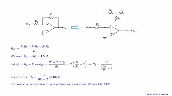
Vo
Vi
R′2
Vo
Vi
R2R′1
R′1
R1 R3
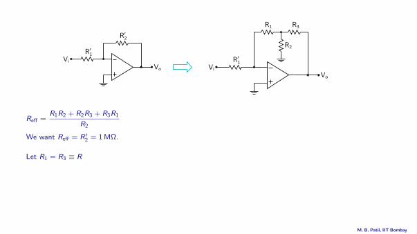
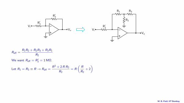
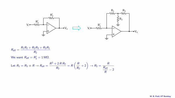
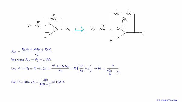
Reff =R1R2 + R2R3 + R3R1
R2
We want Reff = R′2 = 1 MΩ.
Let R1 = R3 ≡ R → Reff =R2 + 2R R2
R2= R
(R
R2+ 2
)→ R2 =
R
Reff
R− 2
For R = 10 k, R2 =10 k
100− 2≈ 102 Ω.
Ref: Wait et al, Introduction to op-amp theory and applications, McGraw-Hill, 1992.
Vo
Vi
10 k
10 k
102Ω
10 k
M. B. Patil, IIT Bombay
Vo
Vi
R′2
Vo
Vi
R2R′1
R′1
R1 R3
Reff =R1R2 + R2R3 + R3R1
R2
We want Reff = R′2 = 1 MΩ.
Let R1 = R3 ≡ R
→ Reff =R2 + 2R R2
R2= R
(R
R2+ 2
)→ R2 =
R
Reff
R− 2
For R = 10 k, R2 =10 k
100− 2≈ 102 Ω.
Ref: Wait et al, Introduction to op-amp theory and applications, McGraw-Hill, 1992.
Vo
Vi
10 k
10 k
102Ω
10 k
M. B. Patil, IIT Bombay
Vo
Vi
R′2
Vo
Vi
R2R′1
R′1
R1 R3
Reff =R1R2 + R2R3 + R3R1
R2
We want Reff = R′2 = 1 MΩ.
Let R1 = R3 ≡ R → Reff =R2 + 2R R2
R2= R
(R
R2+ 2
)
→ R2 =R
Reff
R− 2
For R = 10 k, R2 =10 k
100− 2≈ 102 Ω.
Ref: Wait et al, Introduction to op-amp theory and applications, McGraw-Hill, 1992.
Vo
Vi
10 k
10 k
102Ω
10 k
M. B. Patil, IIT Bombay
Vo
Vi
R′2
Vo
Vi
R2R′1
R′1
R1 R3
Reff =R1R2 + R2R3 + R3R1
R2
We want Reff = R′2 = 1 MΩ.
Let R1 = R3 ≡ R → Reff =R2 + 2R R2
R2= R
(R
R2+ 2
)→ R2 =
R
Reff
R− 2
For R = 10 k, R2 =10 k
100− 2≈ 102 Ω.
Ref: Wait et al, Introduction to op-amp theory and applications, McGraw-Hill, 1992.
Vo
Vi
10 k
10 k
102Ω
10 k
M. B. Patil, IIT Bombay
Vo
Vi
R′2
Vo
Vi
R2R′1
R′1
R1 R3
Reff =R1R2 + R2R3 + R3R1
R2
We want Reff = R′2 = 1 MΩ.
Let R1 = R3 ≡ R → Reff =R2 + 2R R2
R2= R
(R
R2+ 2
)→ R2 =
R
Reff
R− 2
For R = 10 k, R2 =10 k
100− 2≈ 102 Ω.
Ref: Wait et al, Introduction to op-amp theory and applications, McGraw-Hill, 1992.
Vo
Vi
10 k
10 k
102Ω
10 k
M. B. Patil, IIT Bombay
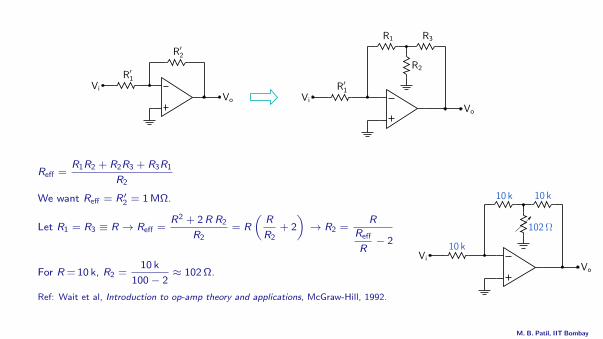
Vo
Vi
R′2
Vo
Vi
R2R′1
R′1
R1 R3
Reff =R1R2 + R2R3 + R3R1
R2
We want Reff = R′2 = 1 MΩ.
Let R1 = R3 ≡ R → Reff =R2 + 2R R2
R2= R
(R
R2+ 2
)→ R2 =
R
Reff
R− 2
For R = 10 k, R2 =10 k
100− 2≈ 102 Ω.
Ref: Wait et al, Introduction to op-amp theory and applications, McGraw-Hill, 1992.
Vo
Vi
10 k
10 k
102Ω
10 k
M. B. Patil, IIT Bombay


