
1
Overview of Optical Metrology for
Ultra-thin Oxide and High-KGate Dielectrics
William W. Chism, Alain C. Diebold, & James M. Price International SEMATECH
March 25, 2003
2
OUTLINE:
1. Current Gate Dielectric Metrology Challenges
2. Implementation of Spectroscopic Ellipsometry to High K/ Ultrathin Oxide Stacked Gate Dielectric Metrology
3. Characterization of Gate Oxide on Silicon-On-Insulator substrates
4. Future Gate Stack Metrology Challenges

3
1. Current Gate Dielectric Metrology Challenges:
High K gate dielectric films exhibit sensitive dependence on material composition—need to control material compositionAlso High K may be stacked on Ultra-thin Oxide interface to preserve channel mobility— need to control interfacial thickness in “EOT” measurement
Review paper: G.D. Wilk, R.M. Wallace, J.M. Anthony, “High K gate dielectrics: current status and materials properties considerations”, J. Appl. Phys., vol. 89, 5243 (2001).
4
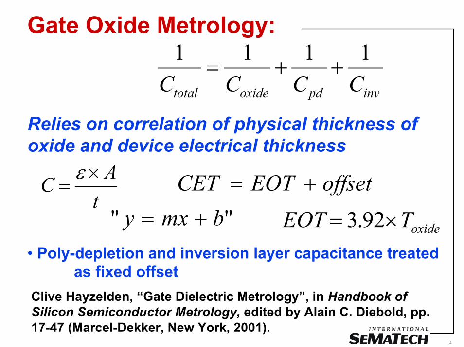
Gate Oxide Metrology:
invpdoxidetotal CCCC1111
++=
Relies on correlation of physical thickness of oxide and device electrical thickness
tAC ×
=ε offsetEOTCET +=
"" bmxy += oxideTEOT ×= 92.3• Poly-depletion and inversion layer capacitance treated
as fixed offsetClive Hayzelden, “Gate Dielectric Metrology”, in Handbook of Silicon Semiconductor Metrology, edited by Alain C. Diebold, pp. 17-47 (Marcel-Dekker, New York, 2001).
5
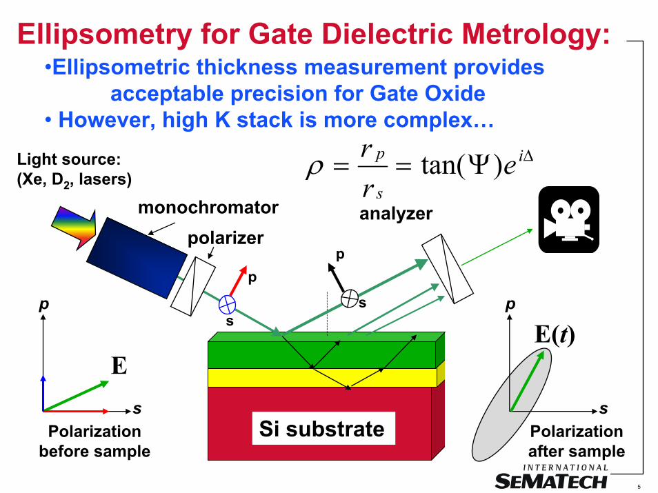
Ellipsometry for Gate Dielectric Metrology:
∆Ψ== i
s
p err )tan(ρ
polarizeranalyzermonochromator
Es
p
Polarizationbefore sample
s
p
E(t)
Polarizationafter sample
p
s
p
s
Si substrate
Light source:(Xe, D2, lasers)
•Ellipsometric thickness measurement provides acceptable precision for Gate Oxide
• However, high K stack is more complex…

6
If dielectric constant of film is known, then only need high K film physical thickness— conclusion in this case is that ellipsometric approach will work
highKhighK
oxide TEOT ×=εε“Ideal” high K ⇒
Ellipsometric approach for High K gate dielectric metrology:
However, high k composition has proven notoriously difficult to control in practice ⇒ now must also track high K film material properties in ellipsometric approachNeed to limit number of fit parameters ⇒ improved precisionNeed appropriate dispersion functional form (ε2 ≠ 0)⇒ improved precision

7
Optical Constants
Photon Energy (eV)0.0 1.0 2.0 3.0 4.0 5.0 6.0 7.0
Inde
x of
refra
ctio
n 'n
'Extinction C
oefficient 'k'
1.6
1.8
2.0
2.2
2.4
2.6
2.8
0.00
0.10
0.20
0.30
0.40
“Medium K”
“Highest K”
“Higher K”
Typical optical response of Hi-K films:
• Index tracks K value— normally will exhibit approximate linearity over process range
8
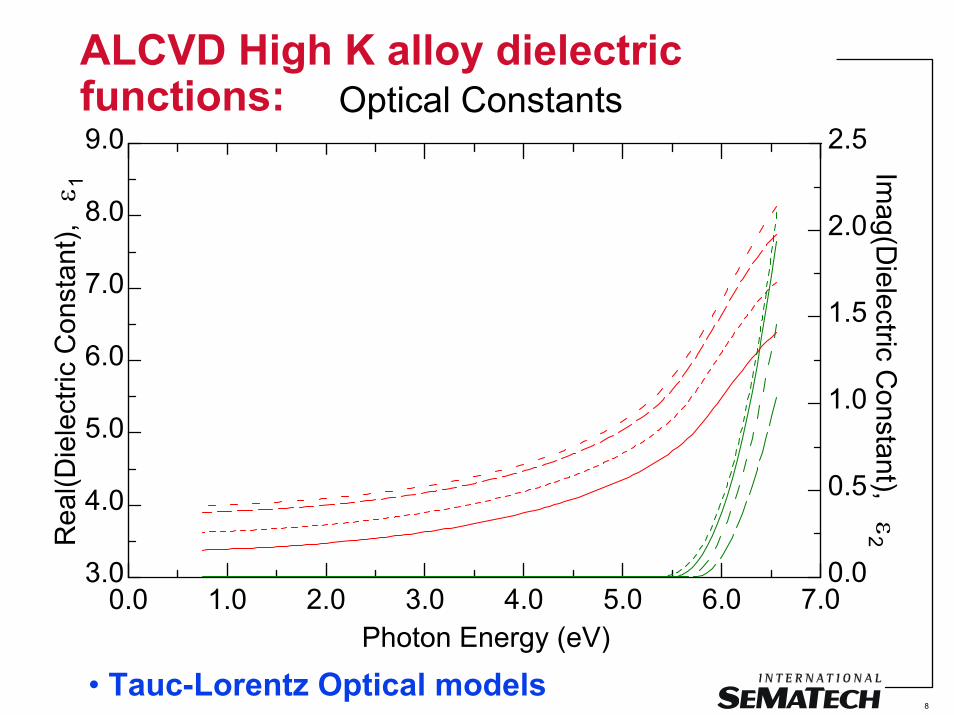
ALCVD High K alloy dielectric functions: Optical Constants
Photon Energy (eV)0.0 1.0 2.0 3.0 4.0 5.0 6.0 7.0
Rea
l(Die
lect
ric C
onst
ant),
ε 1
Imag(D
ielectric Constant),
ε2
3.0
4.0
5.0
6.0
7.0
8.0
9.0
0.0
0.5
1.0
1.5
2.0
2.5
Hf1:Al1, ε1Hf2:Al1, ε1Hf3:Al1, ε1Hf5:Al1, ε1Hf1:Al1, ε2Hf2:Al1, ε2Hf3:Al1, ε2Hf5:Al1, ε2
• Tauc-Lorentz Optical models

9
Typical Tauc-Lorentz fit:
Generated and Experimental
Photon Energy (eV)0.0 1.0 2.0 3.0 4.0 5.0 6.0 7.0
Ψ in
deg
rees
∆in degrees
0
10
20
30
40
50
60
0
30
60
90
120
150
180
Spectroscopic Ellipsometry of ALCVD High K alloys

10
Effective medium approach:
Medium 1e.g: Silicon Dioxide
Medium 2e.g: Silicon Nitride
Effective mediume.g. Oxynitride
Advantages• may combine known material
dispersions • allows calibration to material
composition

11
Nitrogen content determination in oxynitridesvia spectroscopic ellipsometry:
Optical Constants
Photon Energy (eV)1.0 2.0 3.0 4.0 5.0 6.0 7.0
Rea
l(Die
lect
ric C
onst
ant),
ε1
2.0
2.2
2.4
2.6
2.8
3.0
oxide5%nitrogen8%nitrogen10%nitrogen13%nitrogen15%nitrogen

12
Optical Constants
Photon Energy (eV)0.0 1.0 2.0 3.0 4.0 5.0 6.0 7.0
Rea
l(Die
lect
ric C
onst
ant),
ε 1
Imag(D
ielectric Constant),
ε2
3.0
4.0
5.0
6.0
7.0
8.0
0.0
0.5
1.0
1.5
2.0
Tauc-Lor, ε1EMA, ε1Tauc-Lor, ε2EMA, ε2
EMA with Tauc-Lorentz constituents for fitting High K process window:

13
High-K Gate Dielectric Metrology:Real High K has ultra-thin interfacial oxide ⇒
oxidehighKhighK
oxide TTEOT +×=κκPotentially Requires:
1. Hi-K film physical thickness
2. K value 3. Interfacial oxide
thickness Reduced correlation to device performance
Will SE work for Ultra-thin Oxide layers below high K?
• Ellipsometry: sensitive to “total” dielectric physical thickness, but limited sensitivity to interfacial thickness

14
Gate Dielectric Modeling Approach:
3. Hi-K stacked Gate Dielectric on Si
2. Hi-K filmon Si Wafer
1. Gate Oxide on Si Wafer
1. Gate Oxide- Single Wavelength Ellipsometry (laser based) for Tox ⇒ acceptable “EOT”precision
2. “Ideal” High K- Spectroscopic Ellipsometry (lamp based) for material content and Thi-K, ⇒precision too large by ~4x
3. High K/ Ultra-thin Oxide Stack- No Best Known Method established to date
15
OUTLINE:
1. Current Gate Dielectric Metrology Challenges
2. Implementation of Spectroscopic Ellipsometry to High K/ Ultra-thin Oxide Stacked Gate Dielectric
3. Characterization of Gate Oxide on Silicon-On-Insulator substrates
4. Future Gate Dielectric Metrology Challenges
16
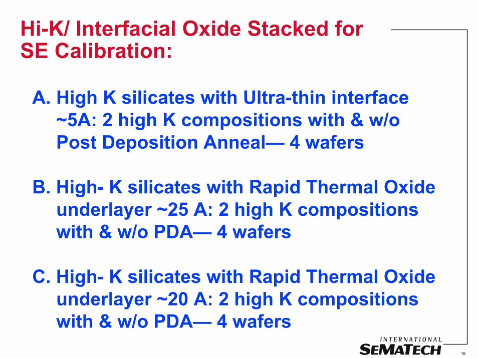
Hi-K/ Interfacial Oxide Stacked for SE Calibration:
A. High K silicates with Ultra-thin interface ~5A: 2 high K compositions with & w/o Post Deposition Anneal— 4 wafers
B. High- K silicates with Rapid Thermal Oxide underlayer ~25 A: 2 high K compositions with & w/o PDA— 4 wafers
C. High- K silicates with Rapid Thermal Oxide underlayer ~20 A: 2 high K compositions with & w/o PDA— 4 wafers

17
HRTEM— Hi-K #2/ Oxide #1
5 nm
2.7 – 3.3 nm high-k2.3 nm SiO2
5 nm
2.9 – 3.4 nm high-k2.0 – 2.3 nm SiO2
Courtesy Brendan Foran, ISMT

18
HRTEM— Hi-K #1/ Oxide #2 with Post Deposition Anneal
5 nm
3.2 – 3.6 nm high-k2.3 nm SiO2
5 nm
3.3 – 3.7 nm high-k2.0 – 2.2 nm SiO2
Courtesy Brendan Foran, ISMT

19
Hi-K/ oxide stack VASE™ results:Generated and Experimental
Wavelength (nm)0 200 400 600 800
Ψ in
deg
rees
∆in degrees
0
10
20
30
40
50
30
60
90
120
150
180
• Rapid Thermal Oxide— independent of PDA

20
Hi-K/ oxide stack VASE™ results:MOCVD High K silicates w/ post deposition anneal
Optical Constants
Photon Energy (eV)0 2 4 6 8 10
Rea
l(Die
lect
ric C
onst
ant),
ε 1
3.0
4.0
5.0
6.0
7.0
Shift seen w/ PDA
Lowermetal content
Higher metal content
21
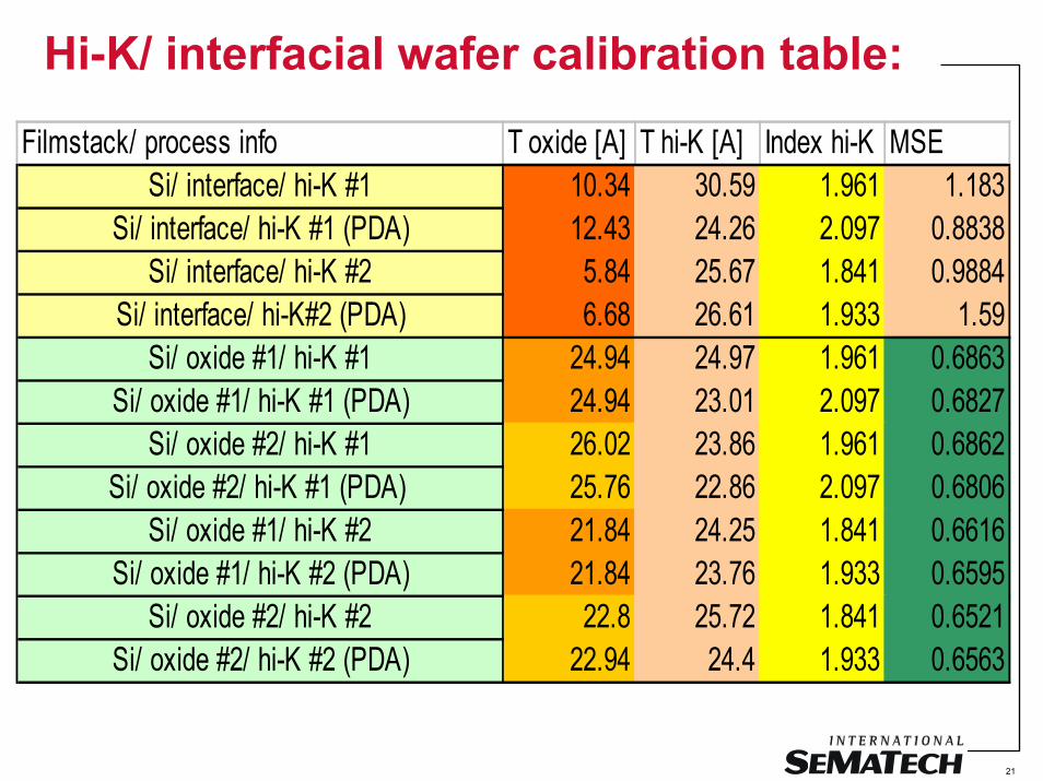
Hi-K/ interfacial wafer calibration table:
Filmstack/ process info T oxide [A] T hi-K [A] Index hi-K MSESi/ interface/ hi-K #1 10.34 30.59 1.961 1.183
Si/ interface/ hi-K #1 (PDA) 12.43 24.26 2.097 0.8838Si/ interface/ hi-K #2 5.84 25.67 1.841 0.9884
Si/ interface/ hi-K#2 (PDA) 6.68 26.61 1.933 1.59Si/ oxide #1/ hi-K #1 24.94 24.97 1.961 0.6863
Si/ oxide #1/ hi-K #1 (PDA) 24.94 23.01 2.097 0.6827Si/ oxide #2/ hi-K #1 26.02 23.86 1.961 0.6862
Si/ oxide #2/ hi-K #1 (PDA) 25.76 22.86 2.097 0.6806Si/ oxide #1/ hi-K #2 21.84 24.25 1.841 0.6616
Si/ oxide #1/ hi-K #2 (PDA) 21.84 23.76 1.933 0.6595Si/ oxide #2/ hi-K #2 22.8 25.72 1.841 0.6521
Si/ oxide #2/ hi-K #2 (PDA) 22.94 24.4 1.933 0.6563

22
High K/ interfacial layer optical metrology summary…
Standard spectroscopic ellipsometric approach parameters strongly coupled— not quite enough precision for interfacial layer thickness or material content
Approach also suffers from decreasing correlation with device characteristics—must account for process step induced changes present
Need to develop interface specific techniques
23
OUTLINE:1. Current Gate Dielectric Metrology
Challenges
2. Implementation of Spectroscopic Ellipsometry to High K/ Ultrathin Oxide Stacked Gate Dielectric
3. Characterization of Gate Oxide on Silicon-On-Insulator substrates
4. Future Gate Dielectric Metrology Challenges

24
Extra reflection from SOI Wafers Impacts Ellipsometric Measurements
SOI WaferSi Wafer
Gate Dielectric on SOI Wafer
Gate Dielectric on Si Wafer

25
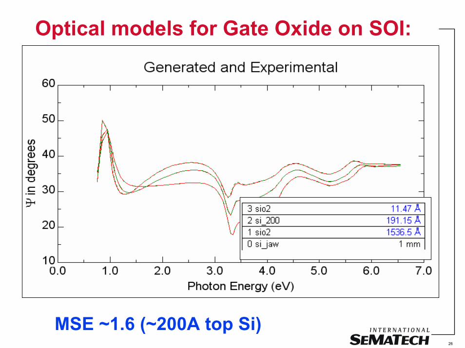
Optical models for Gate Oxide on SOI:
Extra reflection may impact Gate Oxide on SOI precision
26
Optical models for Gate Oxide on SOI:
MSE ~1.6 (~200A top Si)

27
Gate Oxide on SOI substrate optical metrology summary…
Standard spectroscopic ellipsometric approach appears acceptable— excellent fitting seen, impact of extra-reflection needs evaluation
Future High K stack on strained SOI appears likely…
S. Zollner, et al., “Thin-film metrology of silicon-on-insulator materials”, Appl. Phys. Lett. vol. 76, 46 (2001).
28
OUTLINE:1. Current Gate Dielectric Metrology
Challenges
2. Implementation of Spectroscopic Ellipsometry to High K/ Ultrathin Oxide Stacked Gate Dielectric
3. Characterization of Gate Oxide on Silicon-On-Insulator substrates
4. Future Gate Dielectric Metrology Challenges

29
4. Future Gate Dielectric Metrology Challenges:
SE at limits- to characterize:
1. High K gate dielectric on Si substrate
2. High K/ interfacial oxide stack on Si
3. Gate Oxide on SOI
4. Gate Oxide on SiGe
5. Gate Oxide on SiGe-on-Insulator

30
Generated and Experimental
Photon Energy (eV)0.0 1.0 2.0 3.0 4.0 5.0 6.0 7.0
Ψ in
deg
rees
0
10
20
30
40
ModeExp Exp
Ultra-thin Oxide on Graded SiGesubstrate:
31
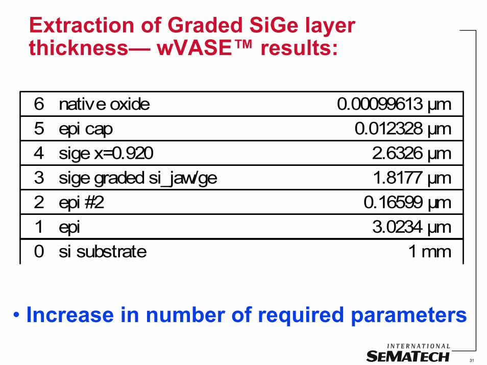
Extraction of Graded SiGe layer thickness— wVASE™ results:
0 si substrate 1 mm1 epi 3.0234 µm2 epi #2 0.16599 µm3 sige graded si_jaw/ge 1.8177 µm4 sige x=0.920 2.6326 µm5 epi cap 0.012328 µm6 native oxide 0.00099613 µm
• Increase in number of required parameters

32
Timeline for Fully Depleted Ultra-thin body SOI–
• 115nm node (2002) SOI ~16-27 nm BOX ~40-66 nm
• 90nm node (2004) SOI ~11-19 nm BOX ~28-46 nm
• 65nm node (2007) SOI ~8-13 nm BOX ~19-31 nm
• 45nm node (2010) SOI ~5-9 nm BOX ~14-23 nm
• 32nm node (2013) SOI ~4-7 nm BOX ~10-16 nm
• 22nm node (2016) SOI: 3-5 nm BOX ~7-11 nmBOX may stay at ~100nm
33
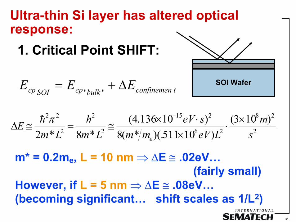
Ultra-thin Si layer has altered optical response:
SOI Wafer
1. Critical Point SHIFT:
tconfinemenbulkcpSOIcp EEE ∆+=""
2
28
26
215
2
2
2
22 )103()10511)(.*(8)10136.4(
*8*2 sm
LeVmmseV
Lmh
LmE
e
×⋅
×⋅×
≅=≅∆−πh
m* = 0.2me, L = 10 nm ⇒ ∆E ≅ .02eV…(fairly small)
However, if L = 5 nm ⇒ ∆E ≅ .08eV…(becoming significant… shift scales as 1/L2)
34
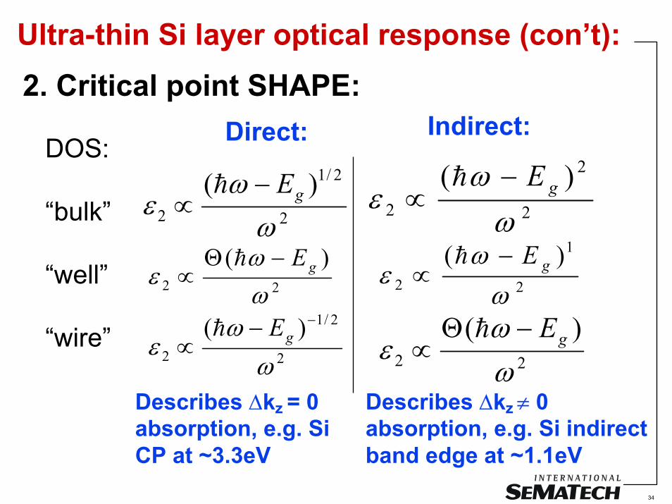
Ultra-thin Si layer optical response (con’t):2. Critical point SHAPE:
Indirect:Direct:DOS:
“bulk”
“well”
“wire”
22
)(ωω
ε gE−Θ∝
h
2
2/1
2
)(ω
ωε gE−∝
h
2
2/1
2
)(ω
ωε
−−∝ gEh
2
2
2
)(ω
ωε gE−∝
h
Describes ∆kz ≠ 0 absorption, e.g. Si indirect band edge at ~1.1eV
2
1
2
)(ω
ωε gE−
∝h
22
)(ωω
ε gE−Θ∝
h
Describes ∆kz = 0 absorption, e.g. Si CP at ~3.3eV

35
Schematic change in dielectric function of 5nm Si (no shape change):
“bulk”SOI

36
Schematic difference in dielectric function of 50A Si (vs. “bulk”):
Biggest differences occur at structural features (CP shape change critical)

37
Extraction of Ultrathin body SOI optical response:
)exp( zII
o
α−=nk21~2 =ελπα k4
=
AzAn 50,3760,9.6,12 ≅≅≅≅∆ λε
%9937609.62504exp ≈
⋅⋅⋅
−≈π
oII
⇒ Need ~1% differential intensity resolution, with resolution in photon energy of <.01eV, on a strongly absorbing background…

38
Future Gate DielectricMetrology:
• Future gate stack projected to be High-K on SiGe-on-Insulator
• For High K/ oxide gate stack SE approach will need to be enhanced
• Optical Metrology for correlation to substrate characteristics may also be required

39
Acknowledgements:
Billy Nguyen, Todd Rhoad, & ISMTNhan Nguyen, Curt Richter, & NISTSue Kelso, Youxian Wen, & Therma-WaveTom Tiwald & J.A. Woollam Co.Stefan Zollner, Motorola
… and many others


![[TA1-D] Hybrid Oxide Thin Films](https://cdn.vdocument.in/doc/165x107/615ab33bad71057f9352b7b6/ta1-d-hybrid-oxide-thin-films.jpg)
