Paradee Leerungnawarat
Department of Materials Science and Engineering

Introduction
What is SiC?
Why SiC?• SiC has many advantages over Si.• It is widely used for high power, high temperature electronic devices.
Why High-Density Plasma?• It is very difficult to wet etch (practicality).• Conventional Reactive Ion Etching produces very low etch rates

3C-SiC 4H-SiC
6H-SiC
Silicon Carbide Crystal Structure

Silicon carbide properties
Properties 3C-SiC 6H-SiC 4H-SiC Si
Indirect Indirect Indirect IndirectBandgap (300 K, eV)
2.3 3.0 3.2 1.12
Electron Mobility (cm2/V-s)
@ room temperature, doping~1016 cm-3
750 370 800 1100
Hole Mobility (cm2/V-s)
@ room temperature, doping~1016 cm-3
40 90 115 420
Breakdown field (MV/cm)
@ doping~1016 cm-3
>1.5 3.2 3.0 0.6
Thermal Conductivity (W/cm-K)
@ room temperature, doping~1017 cm-3
3.2 4.9 3.7 1.5
Electron drift velocity (107 cm/s) 2.5 2.0 2.0 1.0
Dielectric constant, εε 9.7 9.7 9.7 11.8
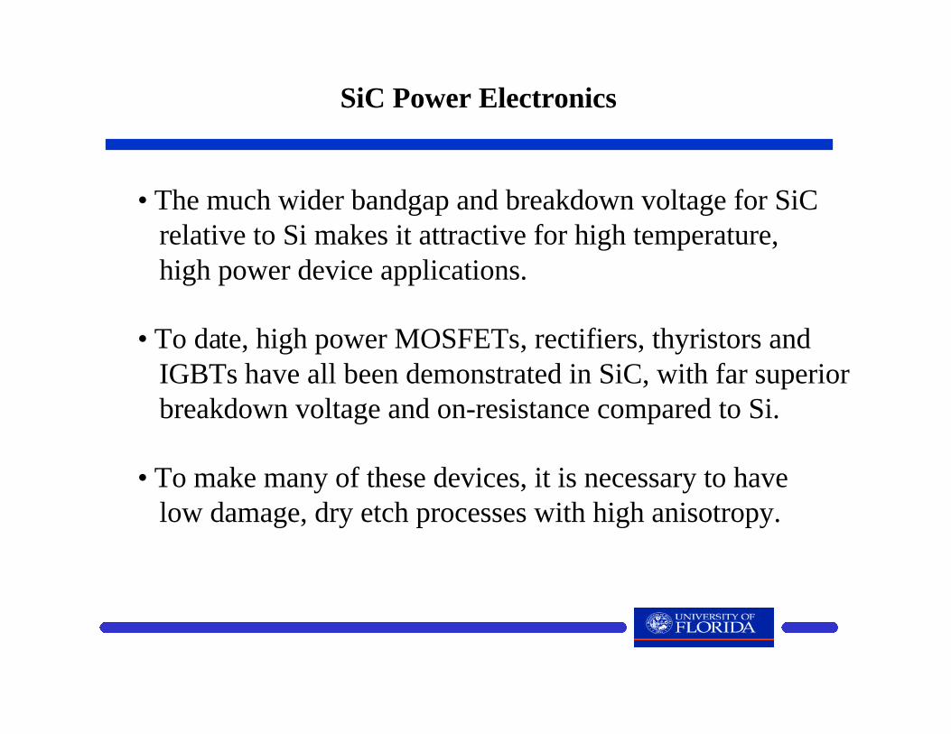
SiC Power Electronics
• The much wider bandgap and breakdown voltage for SiC relative to Si makes it attractive for high temperature, high power device applications.
• To date, high power MOSFETs, rectifiers, thyristors and IGBTs have all been demonstrated in SiC, with far superior breakdown voltage and on-resistance compared to Si.
• To make many of these devices, it is necessary to have low damage, dry etch processes with high anisotropy.

Theoretical and Experimental Performance of SiCAnd Si Schottky Rectifiers.
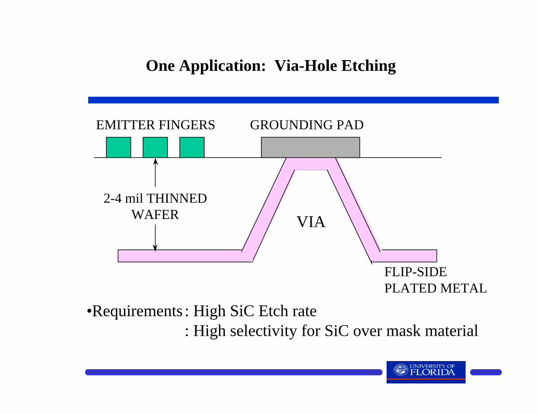
One Application: Via-Hole Etching
VIA
2-4 mil THINNEDWAFER
EMITTER FINGERS GROUNDING PAD
FLIP-SIDEPLATED METAL
•Requirements : High SiC Etch rate: High selectivity for SiC over mask material
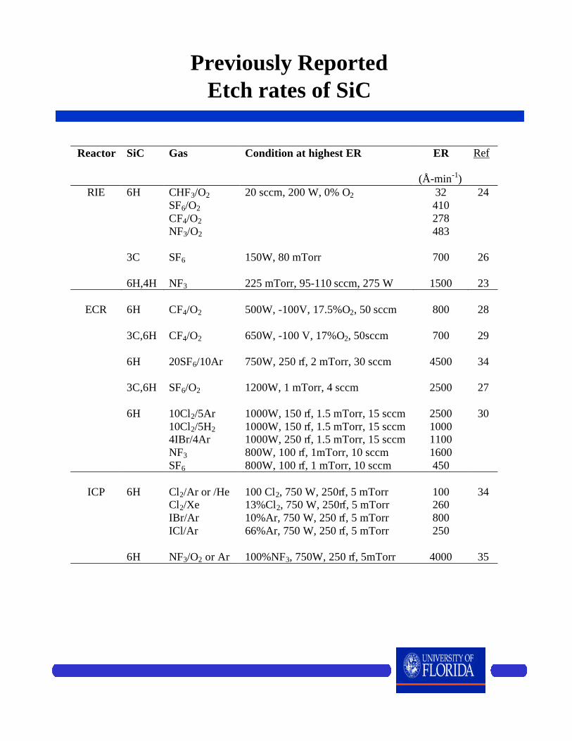
Reactor SiC Gas Condition at highest ER ER
(Å-min-1)
Ref
RIE 6H CHF3/O2 20 sccm, 200 W, 0% O2 32 24SF6/O2 410CF4/O2 278NF3/O2 483
3C SF6 150W, 80 mTorr 700 26
6H,4H NF3 225 mTorr, 95-110 sccm, 275 W 1500 23
ECR 6H CF4/O2 500W, -100V, 17.5%O2, 50 sccm 800 28
3C,6H CF4/O2 650W, -100 V, 17%O2, 50sccm 700 29
6H 20SF6/10Ar 750W, 250 rf, 2 mTorr, 30 sccm 4500 34
3C,6H SF6/O2 1200W, 1 mTorr, 4 sccm 2500 27
6H 10Cl2/5Ar 1000W, 150 rf, 1.5 mTorr, 15 sccm 2500 3010Cl2/5H2 1000W, 150 rf, 1.5 mTorr, 15 sccm 10004IBr/4Ar 1000W, 250 rf, 1.5 mTorr, 15 sccm 1100NF3 800W, 100 rf, 1mTorr, 10 sccm 1600SF6 800W, 100 rf, 1 mTorr, 10 sccm 450
ICP 6H Cl2/Ar or /He 100 Cl2, 750 W, 250rf, 5 mTorr 100 34Cl2/Xe 13%Cl2, 750 W, 250rf, 5 mTorr 260IBr/Ar 10%Ar, 750 W, 250 rf, 5 mTorr 800ICl/Ar 66%Ar, 750 W, 250 rf, 5 mTorr 250
6H NF3/O2 or Ar 100%NF3, 750W, 250 rf, 5mTorr 4000 35
Previously ReportedEtch rates of SiC
High-Density Plasma
• In this work we employ a form of high density plasma (Inductive Coupled Plasma) and several different F2-based gas chemistries.
• HDP provides high ion flux, low ion energy and efficient plasma dissociation : low damage, high rate etching.
• We examined the active plasma species by Optical Emission Spectroscopy (OES) in order to understand the etch mechanism.
• We also examined several different mask materials (Al, ITO and Ni).
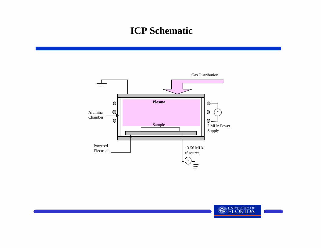
ICP Schematic
~
13.56 MHzrf source
Gas Distribution
AluminaChamber
PoweredElectrode
Plasma
Sample
~
2 MHz PowerSupply
n
n nn
nn
n
neee
ei
ie
nn
n n
s
abs des
n s
n
diff
i
acc
s s
s ssputsput
n n
i
s s
abs des
s-n
abs
n
i
s
sput
n s
n
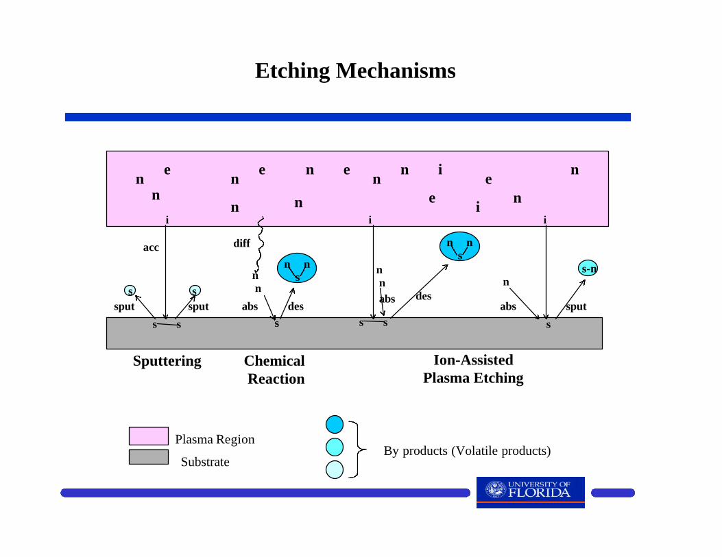
Plasma Region
SubstrateBy products (Volatile products)
Etching Mechanisms
Sputtering Chemical Reaction
Ion-AssistedPlasma Etching

Keys to SiC Etching
• Must break strong Si-C bonds in order to allow etch products to form.
• Expect SiFx and CFx to be the etch products (These are much more volatile than SiClx and CClx, and hence F2- based plasma chemistries are favored over Cl2-based chemistries).

Experiment
ICP reactor2 mTorr15 sccm
Gas : NF3, BF3, SF6 or PF5ICP source power: 750, 1000, 1250,1500 WRf chuck power: 150, 250, 350, 450 WOptical Emission Spectroscopy (OES)
Etcheddepth
measurementStylus Profilometer(Tencor)
RoughnessMeasurement Atomic Force Microscope
1. 4H-SiC2. Al3. Ni4. ITO
Mask withApiezon wax

ICP-Power (W)750 1000 1250 1500
Etc
h Y
ield
(at
om/io
n)
0
1
2
3
4
PF5BF3SF6NF3
750 1000 1250 1500
Etc
h R
ate
(Å/m
in)
1000
4000
6000
8000
10000 PF5BF3SF6NF3
250W rf, 2 mTorr, 15 sccm
250W rf, 2 mTorr, 15 sccm
Etch rate in different ICP Power in four different gases

Inte
nsity
(A
rb. U
.)
3
6
9100 BF3
1500W ICP5W rf35mTorr
Wavelength (nm)
200 400 600 800
Inte
nsity
(A
rb. U
.)
3
6
9100 PF5
1500W ICP5W rf35mTorr
B
SiFx
F
F
F F
P SiFx
F
F F
Inte
nsity
(A
rb. U
.)
5
10
15
20100NF3
1500W ICP5W rf35mTorr
Wavelength (nm)
200 400 600 800
Inte
nsity
(A
rb. U
.)
2
4
6100SF6
1500W ICP5W rf35mTorr
F
F F
F F
F F
SiFx
Chemical Bond Strength(KCal/mol)
NF3 66.4
SF6 78.3
PF5 126
BF3 154
Dissociation Energiesand OES Spectra
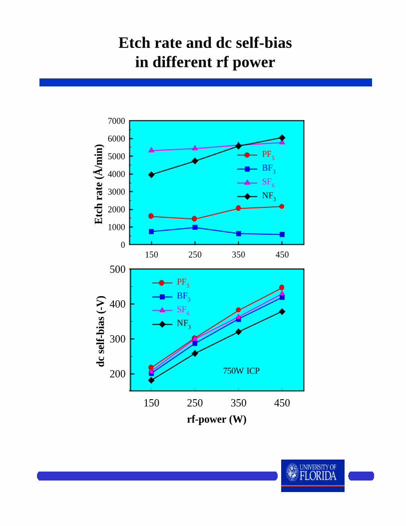
rf-power (W)
150 250 350 450
dc s
elf-
bias
(-V
)
200
300
400
500PF5
BF3
SF6
NF3
150 250 350 450
Etc
h ra
te (Å
/min
)
0
1000
2000
3000
4000
5000
6000
7000
PF5
BF3
SF6
NF3
750W ICP
Etch rate and dc self-biasin different rf power

SiC
Control : RMS = 2.5 nm
PF5: RMS = 2.0 nm BF3 : RMS = 0.8 nm
NF3 : RMS = 0.6 nmSF6 : RMS = 1.4 nm
1500 W Source Power250 W rf chuck power1 minute
Surface roughness data from AFM

ICP-Power (W)750 1000 1250 1500
RM
S (n
m)
0
1
2
3
4PF5
BF3
SF6
NF3Control
Surface roughness in difference gases
• Surface may actually become
smoother due to the angular dependence of ion milling which leads to faster removal of sharp features on the surface.
θθ
+
ER
0 90θθ

ICP power (W)
0 200 400 600 800 1000 1200
Etc
h R
ate
(Å/m
in)
0
1000
2000
3000
4000
5000
dc
self
-bia
s (-
V)
150
200
250
300
350
400
450
500
UV w/o UVdc self-bias
Etching in 10SF6/5Arw and w/o UV
rf power (W)
50 100 150 200 250 300
Etc
h R
ate
(Å/m
in)
0
1000
2000
3000
4000
dc s
elf-
bias
(-V
)
150
200
250
300
350
UV w/o UVdc self-bias
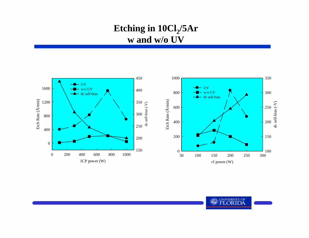
ICP power (W)
0 200 400 600 800 1000
Etc
h R
ate
(Å/m
in)
0
400
800
1200
1600
dc s
elf-
bias
(-V
)150
200
250
300
350
400
450
UV w/o UVdc self-bias
Etching in 10Cl2/5Arw and w/o UV
rf power (W)
50 100 150 200 250 300
Etc
h R
ate
(Å/m
in)
0
200
400
600
800
1000
dc s
elf-
bias
(-V
)
100
150
200
250
300
350
UV w/o UVdc self-bias
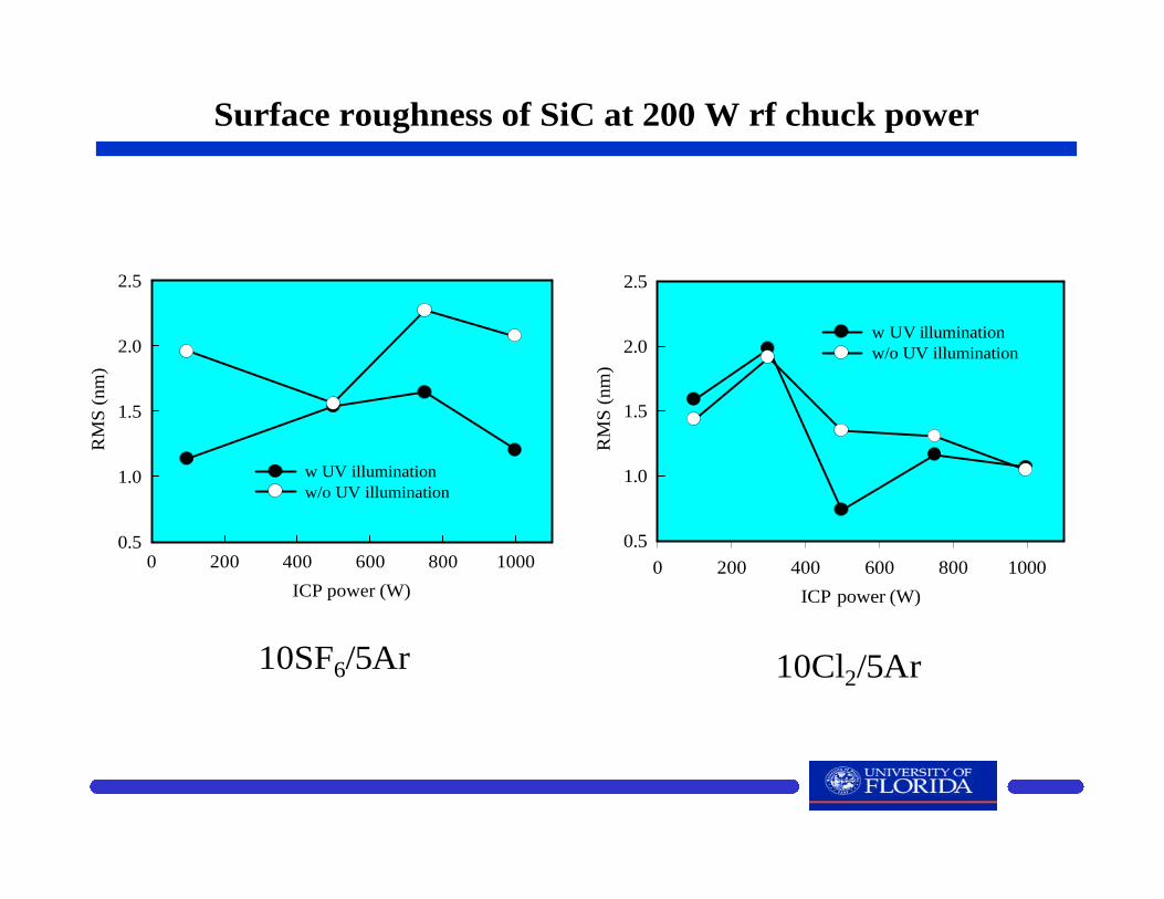
ICP power (W)
0 200 400 600 800 1000
RM
S (
nm)
0.5
1.0
1.5
2.0
2.5
w UV illuminationw/o UV illumination
ICP power (W)
0 200 400 600 800 1000
RM
S (
nm)
0.5
1.0
1.5
2.0
2.5
w UV illuminationw/o UV illumination
10SF6/5Ar 10Cl2/5Ar
Surface roughness of SiC at 200 W rf chuck power

SEM: SiC surface, etches with SF6
W/O UV
With UV
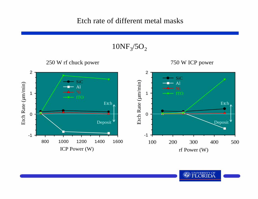
ICP Power (W)
800 1000 1200 1400 1600
Etc
h R
ate
(µm
/min
)
-1
0
1
2
SiCAlNiITO
rf Power (W)
100 200 300 400 500E
tch
Rat
e (µ
m/m
in)
-1
0
1
2SiCAlNiITO
Etch
Deposit
Etch
Deposit
10NF3/5O2
250 W rf chuck power 750 W ICP power
Etch rate of different metal masks

Etc
h R
ate
(µm
/min
)
-0.5
0.0
0.5
1.0SiCAlNiITO
%NF3
(Total flow NF3/O2 is 15 sccm)
20 40 60 80 100
Sele
ctiv
ity
0
3
6
9
12
15
18
21SiC/AlSiC/NiSiC/ITO
Infinite
Etching
Deposition
Etch rate and selectivity in various gas ratio
SUMMARY
• NF3 achieved the highest etch rate up to 8000 Å/minwhich is a result of its higher dissociation efficiency in theICP source.• With high O2 addition to NF3 , very high etch selectivityfor SiC over Al achieved due to oxidation of Al.• With very low O2 concentration, Ni mask shows betterperformance.• UV illumination can increase the etch rate of SiC in Cl2discharge but not in SF6 discharge.• UV illumination can improve surface morphology of SiCin SF6 discharge but not in Cl2 discharge.


