
PCB Via Analysis in Microwave Simulation Model Liu Erli, Zhao Lianqing
School of Electrical and Electronic Engineering ,North China Electric Power University,Beijing, China,102206
[email protected],[email protected]
Abstract: PCB via effect on high-frequency signals can not be ignored in modern circuit design. Based on mi-crowave theory, a dual-port network model of via is established in this paper and the mathematical model about the relationship between the frequency and S21 is brought out. The validity of the theoretical approach is verified by comparing the simulation results of different vias using Ansoft HFSS. In the end some design guidelines are advanced in high-speed PCB design.
Keywords: via; high-speed PCB; signal transmission; dual-port network
1. Introduction
In the design of digital systems, the wiring density
and clock frequency are continuously improving. Signal
integrity, electromagnetic compatibility and other issues
become more serious, so board-level hardware design
becomes more difficult. In the multi-layer PCB, via is
usually used for electrical connections between dif-
ferent layers. In the high-frequency circuits (above 1
GHz) design , the impact of via parasitic parameters
on the signal integrity can’t be ignored and its effect has
become one of the key constraints that its improper han-
dling may lead to failure of the whole design[1].
2. Via Structure
As an important component in multilayer design, via
can be used for fixing device and electrical connections
between different layers .A typical via consists of three
parts: hole, pad area surrounding the hole and clearance
hole in power plane[2].Fig.1 shows a typical via structure.
As Fig.2 shows, via in general is divided into three cate-
gories: blind via, through-hole via and buried via. Blind
via which is located at the top and bottom PCB surfaces
has a certain depth, is often used for connecting the sur-
face and the inner line and its hole depth and diameter
don’t normally exceed a certain ratio. Buried via which
is used to connect PCB inner planes will not extend to
the surface of the board. Through-hole via which
crosses through the entire circuit board is used to achieve
interconnection or internal components installed as a
hole location. As through-hole via is much more easy to
implement and cost less, it is widely used in PCB design.
Fig.1 A typical via structure
3. S21 Model of Via
For further analysis of via, the equivalent model is
established. Each via contains parasitic capacitance and
parasitic inductance which does more harm to
high-frequency signal than the former.Fig.3 shows the
equivalent model of via.
In the microwave point of view, a via can be equiv-
alent to a dual-port network.Fig.4 shows a typical
dual-port network[4], a port inputs signals and the other
outputs signals. If Port1 is defined input port and Port2
defined output port, S21 is on behalf of the Transmission Project Supported by the international science and tech-nology cooperation program(Grant Nos: 2007DFA71250)
141
Proceedings of 14th Youth Conference on Communication
978-1-935068-01-3 © 2009 SciRes.
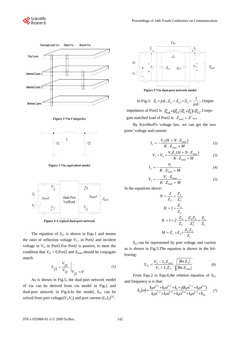
Figure 2 Via Categories
LC1 C2
Figure 3 Via equivalent model
Figure 4 A typical dual-port network
The equation of S21 is shown in Equ.1 and means
the ratio of reflection voltage V2 r in Port2 and incident
voltage in V1i in Port1.For Port2 is passive, to meet the
condition that V2i = 0,Port2 and Zload should be conjugate
match.
0i2
Vi1V
r2V
21S
(1)
As is shown in Fig.5, the dual-port network model
of via can be derived from via model in Fig.1 and
dual-port network in Fig.4.In the model, S21 can be
solved from port voltage(V1,V2) and port current (I1,I2)[5].
Figure 5 Via dual-port network model
In Fig.5: LjZL ,Cj
1ZZZ C2c1c
, Output
impedance of Port2 is , Conju-
gate matched load of Port2 is . 212 //)//( CLsCout ZZZZ
2outload ZZ *
Z
By Kirchhoff's voltage law, we can get the two
ports’ voltage and current:
MZK
ZNHVI
load
loads1
)( (2)
MZK
ZNHZVVV
load
loadssS1
)( (3)
MZK
VI
load
s2
(4)
MZK
ZVV
load
loads2
(5)
In the equations above:
2C
L
C Z
Z
Z
2N
C
L
Z
Z1H
C
L2C
SL
C
S
Z
Z
Z
ZZ
Z
Z21K
c
SLLs Z
ZZZZM
S21 can be represented by port voltage and current
as is shown in Fig.5.The equation is shown in the fol-
lowing:
load
S
S11
2out2221 Z
Z
ZIV
ZIVS
Re
Re
(6)
From Equ.2 to Equ.6,the relation equation of S21
and frequency w is that:
10
219
238
257
276
235
2743
232
251
21 kkkkk
kkjkkkS
////
//// )(
(7)
142
Proceedings of 14th Youth Conference on Communication
978-1-935068-01-3 © 2009 SciRes.

In the above equation, ki is a expression that has nothing
to do with w and k6>k4 .
From Equation 6 and 7,we can know |S21|<1.In the
microwave point of view, via is a loss component. In
the case of fixed parasitic parameters, the frequency of
signals directly determine the value of S21 that the
higher the signal frequency is, the greater the via loss is,
the smaller S21 is. In this paper ,Ansoft is used for via
simulation to validate the relation between the signal
frequency and S21.
4. Simulation of Via effect
Before the simulation, it’s necessary to explain
that via simulation in this paper is used for comparison
between different models and the results can’t represent
the real via. In the models, the main physical (package)
parameters are that substrate is FR-4 (εr = 4.4),both the
thickness of copper plating and via plating are 1oz.In
the following paper, we will establish three different
models for through-hole via, buried via and blind via to
verify the relation between the signal frequency and S21
as is shown in Equation 6 and7.
As is shown in Figure 2, the via is divided into
three categories: blind via, through-hole via and buried
via. Different models have different effect on high fre-
quency signals, that’s to say the trends of S21 are differ-
ent. In this paper, the model of through-hole via has two
layers(bottom layer, top layer),the simulation result of
S21 is shown in Figure 6;the model of blind via has four
layers(top layer, bottom layer, internal layer1,internal
layer2),the simulation result of S21 is shown in Figure
7;the model of buried via has six layers(top layer, bot-
tom layer, internal layer1,internal layer2,power layer,
ground layer), the simulation result of S21 is shown in
Figure 8.
As is shown in Figure 6,in through-hole via model
the value curve of S21 (dB) decline gradually with the
increase in the frequency that the loss of the signals that
transmit from Port1 to Port2 is increasing gradually.
The result is in line with the Equ.6 and7.As is shown in
Fig.7,in blind via model ,the value curve of S21 (dB)
decreases steeply when the frequency is between 1~
2GHz, has some fluctuations when the frequency is
between 2~16GHz.But on the whole the result is in
line with the Equations.6 and7.As is shown in Figure 8,
the value curve of S21 (dB) increases gradually when the
frequency is between 1~2.7GHz and has some fluctua-
tions when the frequency is between3~8GHz.On the
whole the result is not in line with the Equ.6 and7.The
result shows that the electromagnetic environment
around the buried via which is located between the
layers and is near the power layer and ground layer is so
complex that a more effective model should be build to
represent it.
5. Conclusion In high-frequency, high-density PCBs, the loss of through-hole via and blind via would increase with the increasing frequency. As the complexity of he electro-magnetic environment, the buried via which needs a more effective model has no regular change trend. In short, in order to avoid the parasitic parameters of via effect on high frequency signals, the designers should pay more attention to the following advices: ①Minimize unnecessary via; ② Minimize the length of via and Back-Drilling technology can be used to reduce parasitic parameters; ③ Choose a reasonable via diameter. The size on power and ground layers can be more large to reduce the impedance. In the consideration of cost the signal lines can reduce the via diameter.
Figure 6 S21 simulation result of through-hole via
143
Proceedings of 14th Youth Conference on Communication
978-1-935068-01-3 © 2009 SciRes.
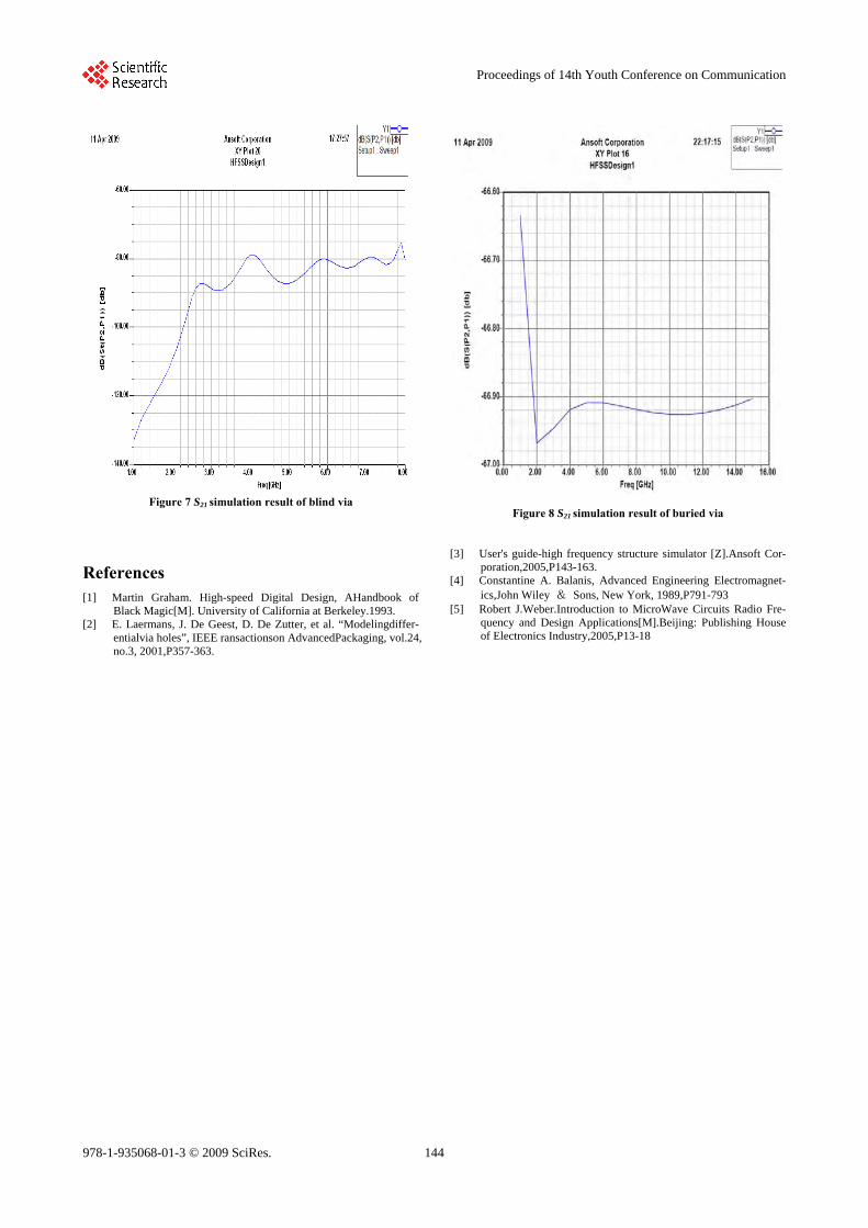
Figure 7 S21 simulation result of blind via
Figure 8 S21 simulation result of buried via
References [1] Martin Graham. High-speed Digital Design, AHandbook of
Black Magic[M]. University of California at Berkeley.1993. [2] E. Laermans, J. De Geest, D. De Zutter, et al. “Modelingdiffer-
entialvia holes”, IEEE ransactionson AdvancedPackaging, vol.24, no.3, 2001,P357-363.
[3] User's guide-high frequency structure simulator [Z].Ansoft Cor-poration,2005,P143-163.
[4] Constantine A. Balanis, Advanced Engineering Electromagnet-ics,John Wiley & Sons, New York, 1989,P791-793
[5] Robert J.Weber.Introduction to MicroWave Circuits Radio Fre-quency and Design Applications[M].Beijing: Publishing House of Electronics Industry,2005,P13-18
144
Proceedings of 14th Youth Conference on Communication
978-1-935068-01-3 © 2009 SciRes.


