Download - PIEZO FILTERS INTRODUCTION
430 CG01-I
PIEZO FILTERSINTRODUCTION
For more than two decades, ceramicfilter technology has been instrumentalin the proliferation of solid stateelectronics. A view of the future revealsthat even greater expectations will beplaced on piezoelectric material in thearea of new applications and for morestringent performance criteria in currentproducts. Traditionally, nearly all lowand high-end AM and FM commercialradios use ceramic band-pass filters.However, applications are also found incordless telephones, cellular systems,2-way communications, and thetelevision industry.
As a world leader in the development of piezo ceramic filter technology,Murata Electronics had been able todevelop specialized ceramic materialswhich when combined with an advancefilter design have resulted in a completeline of practical, inexpensive ceramicfilters for entertainment and communi-cations applications. In this catalog, the principle of ceramic filters, thedesign of representative test circuits
and specifications concerning various models are described.
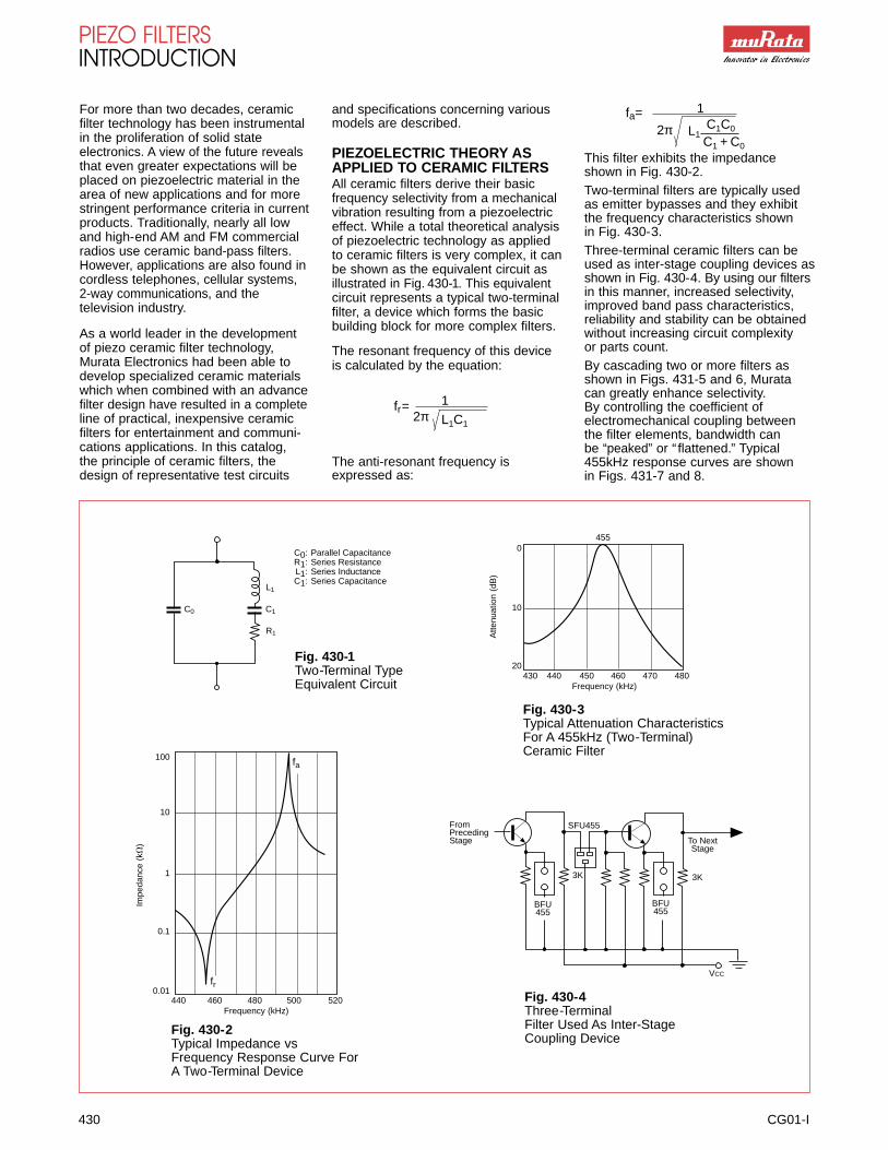
PIEZOELECTRIC THEORY ASAPPLIED TO CERAMIC FILTERSAll ceramic filters derive their basicfrequency selectivity from a mechanicalvibration resulting from a piezoelectriceffect. While a total theoretical analysisof piezoelectric technology as appliedto ceramic filters is very complex, it canbe shown as the equivalent circuit asillustrated in Fig. 430-1. This equivalentcircuit represents a typical two-terminalfilter, a device which forms the basicbuilding block for more complex filters.
The resonant frequency of this deviceis calculated by the equation:
The anti-resonant frequency isexpressed as:
This filter exhibits the impedanceshown in Fig. 430-2.Two-terminal filters are typically usedas emitter bypasses and they exhibitthe frequency characteristics shown in Fig. 430-3.Three-terminal ceramic filters can beused as inter-stage coupling devices asshown in Fig. 430-4. By using our filtersin this manner, increased selectivity,improved band pass characteristics,reliability and stability can be obtainedwithout increasing circuit complexity or parts count.By cascading two or more filters asshown in Figs. 431-5 and 6, Murata can greatly enhance selectivity. By controlling the coefficient ofelectromechanical coupling betweenthe filter elements, bandwidth can be “peaked” or “ flattened.” Typical455kHz response curves are shown in Figs. 431-7 and 8.
fr=1
2π L1C1
fa= 1
2π L1C1C0
C1 + C0
L1
C0 C1
R1
C0: Parallel CapacitanceR1: Series ResistanceL1: Series InductanceC1: Series Capacitance
Fig. 430-1Two-Terminal TypeEquivalent Circuit
Atte
nuat
ion
(dB
)
0
10
20430 440 450 460 470 480
Frequency (kHz)
Fig. 430-3Typical Attenuation CharacteristicsFor A 455kHz (Two-Terminal)Ceramic Filter
Fig. 430-4Three-TerminalFilter Used As Inter-StageCoupling Device
FromPrecedingStage
SFU455
To NextStage
3K
BFU455
VCC
3K
BFU455
Impe
danc
e (k
�)
100
10
1
0.1
0.01440 460 480 500 520
Frequency (kHz)
Fig. 430-2Typical Impedance vsFrequency Response Curve ForA Two-Terminal Device
455
fr
fa
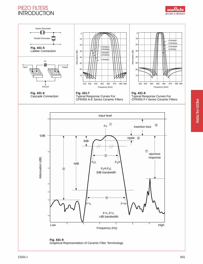
Fig. 431-6 Fig. 431-7 Fig. 431-8Cascade Connection Typical Response Curves For Typical Response Curves For
CFR455 A-E Series Ceramic Filters CFR455 F-I Series Ceramic Filters
Fig. 431-9Graphical Representation of Ceramic Filter Terminology
PIEZO FILTERSINTRODUCTION
�
�
�
�
�
�
�
Series Resonator
Parallel Resonator
Input Output
Cc
Ground
Fig. 431-5Ladder Connection
0
10
20
30
40
50
60
70
420 430 440 450 460 470 480 490
Frequency (kHz)
CFR455ACFR455B
CFR455CCFR455D
CFR455E
0
10
20
30
40
50
60
70
420 430 440 450 460 470 480 490
Frequency (kHz)
CFR455FCFR455G
CFR455HCFR455I
Atte
nuat
ion
(dB
)
Atte
nuat
ion
(dB
)
input level
Fo insertion loss
ripple
spuriousresponse
F�L F�H
F�L-F�L�dB bandwidth
F3H-F3L3dB bandwidth
F3L F3H
3dB
XdB
LowFrequency (Hz)
High
Atte
nuat
ion
(dB
)
0dB
CG01-I 431
PIE
ZO
FILT
ER
S
432 CG01-I
PIEZO FILTERSINTRODUCTION
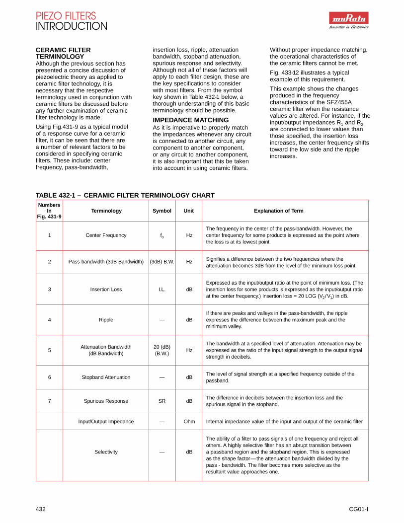
CERAMIC FILTERTERMINOLOGYAlthough the previous section haspresented a concise discussion ofpiezoelectric theory as applied toceramic filter technology, it isnecessary that the respectiveterminology used in conjunction withceramic filters be discussed beforeany further examination of ceramicfilter technology is made.
Using Fig.431-9 as a typical model of a response curve for a ceramic filter, it can be seen that there are a number of relevant factors to beconsidered in specifying ceramicfilters. These include: centerfrequency, pass-bandwidth,
insertion loss, ripple, attenuationbandwidth, stopband attenuation,spurious response and selectivity.Although not all of these factors willapply to each filter design, these arethe key specifications to consider with most filters. From the symbol key shown in Table 432-1 below, athorough understanding of this basicterminology should be possible.
IMPEDANCE MATCHINGAs it is imperative to properly matchthe impedances whenever any circuitis connected to another circuit, anycomponent to another component, or any circuit to another component, it is also important that this be takeninto account in using ceramic filters.
Without proper impedance matching,the operational characteristics of the ceramic filters cannot be met.
Fig. 433-12 illustrates a typicalexample of this requirement.
This example shows the changesproduced in the frequencycharacteristics of the SFZ455Aceramic filter when the resistancevalues are altered. For instance, if theinput/output impedances R1 and R2are connected to lower values thanthose specified, the insertion lossincreases, the center frequency shiftstoward the low side and the rippleincreases.
NumbersIn Terminology Symbol Unit Explanation of Term
Fig. 431-9
The frequency in the center of the pass-bandwidth. However, the 1 Center Frequency fo Hz center frequency for some products is expressed as the point where
the loss is at its lowest point.
2 Pass-bandwidth (3dB Bandwidth) (3dB) B.W. Hz Signifies a difference between the two frequencies where the attenuation becomes 3dB from the level of the minimum loss point.
Expressed as the input/output ratio at the point of minimum loss. (The3 Insertion Loss I.L. dB insertion loss for some products is expressed as the input/output ratio
at the center frequency.) Insertion loss = 20 LOG (V2/V1) in dB.
If there are peaks and valleys in the pass-bandwidth, the ripple4 Ripple — dB expresses the difference between the maximum peak and the
minimum valley.
Attenuation Bandwidth 20 (dB)The bandwidth at a specified level of attenuation. Attenuation may be
5(dB Bandwidth) (B.W.)
Hz expressed as the ratio of the input signal strength to the output signalstrength in decibels.
6 Stopband Attenuation — dBThe level of signal strength at a specified frequency outside of thepassband.
7 Spurious Response SR dBThe difference in decibels between the insertion loss and the spurious signal in the stopband.
Input/Output Impedance — Ohm Internal impedance value of the input and output of the ceramic filter
The ability of a filter to pass signals of one frequency and reject all others. A highly selective filter has an abrupt transition between
Selectivity — dB a passband region and the stopband region. This is expressed as the shape factor—the attenuation bandwidth divided by thepass - bandwidth. The filter becomes more selective as theresultant value approaches one.
TABLE 432-1 – CERAMIC FILTER TERMINOLOGY CHART

CG01-I 433
PIEZO FILTERSINTRODUCTION
On the other hand, if R1 and R2 areconnected to higher values other than those specified, the insertion loss will increase, the center frequencywill shift toward the high side and theripple will increase.
DEALING WITH SPURIOUSRESPONSEFrequently in using 455kHz filters,spurious will cause problems due tothe fact that the resonance occursunder an alien vibrating mode orovertone deviating from the basicvibration characteristics. Amongavailable solutions for dealing withspurious response are:
1. The use of a supplementary IFTtogether with the ceramic filter for suppression of the spurious.
2. The arrangement of two or moreceramic filters in parallel for themutual cancellation of spurious.
3. The addition of a low-pass or high-pass LC filter for suppressionof spurious. Perhaps the mostcommonly used method of dealing
with spurious is the use of asupplementary IFT in conjunctionwith the ceramic filter. The beforeand after effects of the use of an IFT are shown in Figs. 433-10 and 11. In Fig. 433-10, only a singleSFZ455A ceramic filter is employedand spurious is a significantproblem. With the addition of an IFT,the spurious problem is reduced asis shown in Fig. 433-11.
Although spurious is a significantproblem to contend with when using455kHz ceramic filters, it is not aproblem in 4.5MHz and 10.7MHzceramic filters, as their vibration modes are significantly different.
CONSIDERATIONS FOR GAINDISTRIBUTIONSince the impedance of both the input and output values of the ceramicfilters are symmetric and small, it is necessary that the overall gaindistribution within the circuit itself betaken into consideration. For instance,in the discussion concerning properimpedance matching, it was illustrated
that a certain DC loss occurs if therecommended resistance values arenot used. This can cause an overallreduction in the gain which couldpresent a problem if no allowanceshave been made for the correspondingloss. To compensate for this problem, it is recommended that the following be done:
1. The amplifier stage should bedesigned to compensate forthis loss.
2. The ceramic filter should be used in combination with the IFT forminimizing both matching and DClosses. The IFT should be usedstrictly as a matching transformerand the ceramic filter only forselectivity.
As the use of IC’s has become moreprevalent with ceramic filters, theseconsiderations have been taken intoaccount. It should be noted that few of the problems discussed above havebeen realized when more than three(3) IF stages have been employed.
Fig. 433-12Model SFZ455A Ceramic FilterMatching Impedance vs. Pass-BandCharacteristics
Fig. 433-13Coupling With A Transistor
Fig. 433-11Spurious Response With ModelSFZ455A Ceramic Filter And IFT
Fig. 433-10Spurious Response With ModelSFZ455A Ceramic Filter
0 2 4 6 8 10
Frequency (MHz)
0
20
40
60
80
100
Atte
nuat
ion
(dB
)
0
20
40
60
80
100
Atte
nuat
ion
(dB
)
0
10
20
Atte
nuat
ion
(dB
)
0 2 4 6 8 10
Frequency (MHz)
440 450 460 470
Frequency (kHz)
S.S.G.Rg = 50�
Test Circuit
56pF
R1=R2= 6.8k�R1=R2= 3.0k�R1=R2= 560�
R.F.Voltmeter
MatchingCeramic Filters do not pass DC.
DC can be supplied to the transistorby adding a Bias resistor.
The Bias resistor and the Matchingresistor shall be common.
Matching
VB
VB
Bias
Bias and Matching
R1
R2
PIE
ZO
FILT
ER
S

434 CG01-I
CERAMIC FILTERS DO NOT PASS DCIt is important to note in designingcircuits that ceramic filters areincapable of passing DC. As isillustrated in Fig. 433-13, in a typical circuit where a transistor is used, a bias circuit will be required to drive the transistor. Since the ceramic filter requires matching resistance tooperate properly, the matching resistorshown in the diagram can play a dualrole as both a matching and bias resistor.
If the bias circuit is used, it is importantthat the parallel circuit of both the biasresistance and the transistor’s internalresistance be taken into considerationin meeting the resistance values. This is necessary since the internalresistance of the transistor is changedby the bias resistance. However, whenan IC is used, there is no need for anadditional bias circuit since the IC has a bias circuit within itself.
Here it is recommended that an IFT beused for impedance matching with theceramic filter when coupling with amixer stage, as shown in Fig. 434-14.
COUPLING CAPACITANCEThe SFZ455A is composed of two filterelements which must be connected bya coupling capacitor. Moreover, thefrequency characteristic changesaccording to the coupling capacitance(Cc). As shown in Fig. 434-15, thelarger the coupling capacitance (Cc)becomes, the wider the bandwidth andmore the ripple increases. Conversely,the smaller the coupling capacitancebecomes, the narrower the bandwidthbecomes and the more the insertionloss increases. Therefore, the specifiedvalue of the coupling capacitance in thecatalog is desired in determining thespecified passband characteristics.
GROUP DELAY TIMECHARACTERISTICSPerhaps one of the most importantcharacteristics of a transmitting element is to transmit a signal with thelowest possible distortion level. Thisdistortion occurs when the phase shiftof a signal which passes through acertain transmitting path is non-linearwith respect to the frequency. Forconvenience, the group delay time(GDT) characteristic is used for thepurpose of expressing non-linearity.
It is important to note the relationshipbetween the amplitude and the GDTcharacteristics when using group delaytime terminology. This relationshipdiffers depending upon the filtercharacteristics. For example, in theButterworth type, which has a relativelyflat top, the passband is flat while theGDT characteristic is extremely curved,as shown in Fig. 434-16. On the other hand, a Gaussian type, is curved in the passband, while the GDTcharacteristic is flat. With the flat GDT characteristics, the Gaussian type has excellent distortioncharacteristics.
Since the amplitude characteristics for the Butterworth type is flat in the passband the bandwidth does notchange even at a low input level. With the amplitude characteristic for the Gaussian type being curved in the passband, the bandwidth becomesnarrow at a low input level and thesensitivity is poor. Therefore, it should be noted that the Gaussian type has a desirable distortion factorwhile the Butterworth type has thedesirable sensitivity.
Fig. 434-15Model SFZ455A Ceramic Filter Coupling Capacitance vs. PassbandCharacteristics
Fig. 434-14Coupling From Mixer Stage
Fig. 434-16Relationship Between AmplitudeAnd GDT Characteristics
0
10
20Atte
nuat
ion
(dB
)
440 450 460 470
Frequency (kHz)
Amplitude Characteristic
GDT Characteristic
(A) Butterworth Characteristic
Amplitude Characteristic
GDT Characteristic
(B) Gaussian Characteristic
S.S.G.Rg = 50�
Test Circuit
Cc
Cc = 22pFCc = 56pFCc = 100pF
R.F.Voltmeter
R1= 3k�
IFTC.F.
VB
Osc.Mixer
IFAmp.
R1=3k�
PIEZO FILTERSINTRODUCTION
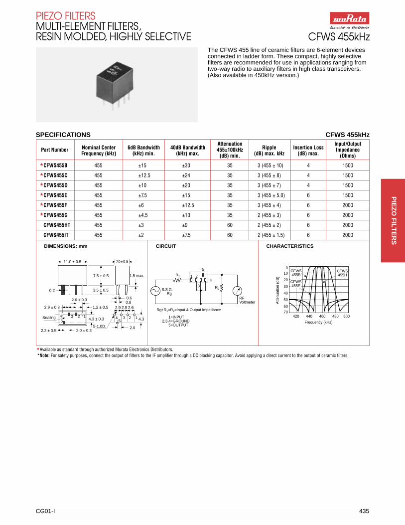
Attenuation Input/OutputPart Number Nominal Center 6dB Bandwidth 40dB Bandwidth 455±100kHz Ripple Insertion Loss Impedance
Frequency (kHz) (kHz) min. (kHz) max. (dB) min. (dB) max. kHz (dB) max. (Ohms)
�CFWS455B 455 ±15 ±30 35 3 (455 ± 10) 4 1500
�CFWS455C 455 ±12.5 ±24 35 3 (455 ± 8) 4 1500
�CFWS455D 455 ±10 ±20 35 3 (455 ± 7) 4 1500
�CFWS455E 455 ±7.5 ±15 35 3 (455 ± 5.0) 6 1500
�CFWS455F 455 ±6 ±12.5 35 3 (455 ± 4) 6 2000
�CFWS455G 455 ±4.5 ±10 35 2 (455 ± 3) 6 2000
CFWS455HT 455 ±3 ±9 60 2 (455 ± 2) 6 2000
CFWS455IT 455 ±2 ±7.5 60 2 (455 ± 1.5) 6 2000
DIMENSIONS: mm CIRCUIT CHARACTERISTICS
SPECIFICATIONS CFWS 455kHz
CG01-I 435
PIEZO FILTERSMULTI-ELEMENT FILTERS,RESIN MOLDED, HIGHLY SELECTIVE CFWS 455kHz
The CFWS 455 line of ceramic filters are 6-element devicesconnected in ladder form. These compact, highly selective filters are recommended for use in applications ranging fromtwo-way radio to auxiliary filters in high class transceivers.(Also available in 450kHz version.)
4 3 2 15
11.0 ± 0.5
7.5 ± 0.5
2.9 ± 0.3
Sealing
3.5 ± 0.5
2.6 ± 0.3
4.3 ± 0.3 45
3 2 1 4.3
2.0 ± 0.32.3 ± 0.55-1.0D.
0.2
2.0
2.9 2.9 2.6
1.5 max.
S.S.G.Rg
RFVoltmeter
420 440 460 480 500
Frequency (kHz)
Atte
nuat
ion
(dB
)
010
20
30
40
50
6070Rg+R1=R2=Input & Output Impedance
1=INPUT2,3,4=GROUND
5=OUTPUT
1 2
34
5R1
R2
0.80.6
7.0±0.5
1.2 ± 0.5
�Available as standard through authorized Murata Electronics Distributors.*Note: For safety purposes, connect the output of filters to the IF amplifier through a DC blocking capacitor. Avoid applying a direct current to the output of ceramic filters.
CFWS455B
CFWS455E
CFWS455H
PIE
ZO
FILT
ER
S
AttenuationPart Number Nominal Center 6dB Bandwidth 40dB Bandwidth 455±100kHz Insertion Loss Input/Output
Frequency (kHz) (kHz) min. (kHz) max. (dB) min. (dB) max. Impedance (Ohms)
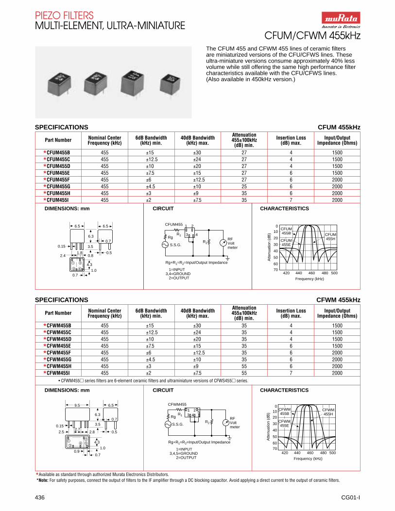
�CFUM455B 455 ±15 ±30 27 4 1500�CFUM455C 455 ±12.5 ±24 27 4 1500�CFUM455D 455 ±10 ±20 27 4 1500�CFUM455E 455 ±7.5 ±15 27 6 1500�CFUM455F 455 ±6 ±12.5 27 6 2000�CFUM455G 455 ±4.5 ±10 25 6 2000�CFUM455H 455 ±3 ±9 35 6 2000�CFUM455I 455 ±2 ±7.5 35 7 2000
DIMENSIONS: mm CIRCUIT CHARACTERISTICS
SPECIFICATIONS CFUM 455kHz
AttenuationPart Number Nominal Center 6dB Bandwidth 40dB Bandwidth 455±100kHz Insertion Loss Input/Output
Frequency (kHz) (kHz) min. (kHz) max. (dB) min. (dB) max. Impedance (Ohms)
�CFWM455B 455 ±15 ±30 35 4 1500�CFWM455C 455 ±12.5 ±24 35 4 1500�CFWM455D 455 ±10 ±20 35 4 1500�CFWM455E 455 ±7.5 ±15 35 6 1500�CFWM455F 455 ±6 ±12.5 35 6 2000�CFWM455G 455 ±4.5 ±10 35 6 2000�CFWM455H 455 ±3 ±9 55 6 2000�CFWM455I 455 ±2 ±7.5 55 7 2000
• CFWM455� series filters are 6-element ceramic filters and ultraminiature versions of CFWS455� series.
DIMENSIONS: mm CIRCUIT CHARACTERISTICS
SPECIFICATIONS CFWM 455kHz
436 CG01-I
PIEZO FILTERSMULTI-ELEMENT, ULTRA-MINIATURE
CFUM/CFWM 455kHzThe CFUM 455 and CFWM 455 lines of ceramic filters are miniaturized versions of the CFU/CFWS lines. Theseultra-miniature versions consume approximately 40% lessvolume while still offering the same high performance filtercharacteristics available with the CFU/CFWS lines.(Also available in 450kHz version.)
� �
� �
1 2
3 4
6.5 6.5
6.3
3.50.15
2.4 0.8
4.3
1.00.7
0.7
0.5
CFUM455
R1Rg
S.S.G.R2
RFVoltmeter
Rg+R1=R2=Input/Output Impedance
1=INPUT3,4=GROUND
2=OUTPUT
��
� ��
1 25
3 4
9.5 6.5
6.3
3.50.15
2.52.7
4.3
1.0
0.7
0.7
0.5
CFWM455
R1Rg
S.S.G.R2
RFVoltmeter
0.9
010
20
30
40
50
60
70420 440 460 480 500
Frequency (kHz)
Atte
nuat
ion
(dB
)
CFUM455B
CFUM455E
CFUM455H
010
20
30
40
50
6070
420 440 460 480 500
Frequency (kHz)
Atte
nuat
ion
(dB
)
CFWM455B
CFWM455E
CFWM455H
1.8
Rg+R1=R2=Input/Output Impedance
1=INPUT3,4,5=GROUND
2=OUTPUT
�Available as standard through authorized Murata Electronics Distributors.*Note: For safety purposes, connect the output of filters to the IF amplifier through a DC blocking capacitor. Avoid applying a direct current to the output of ceramic filters.
2.8
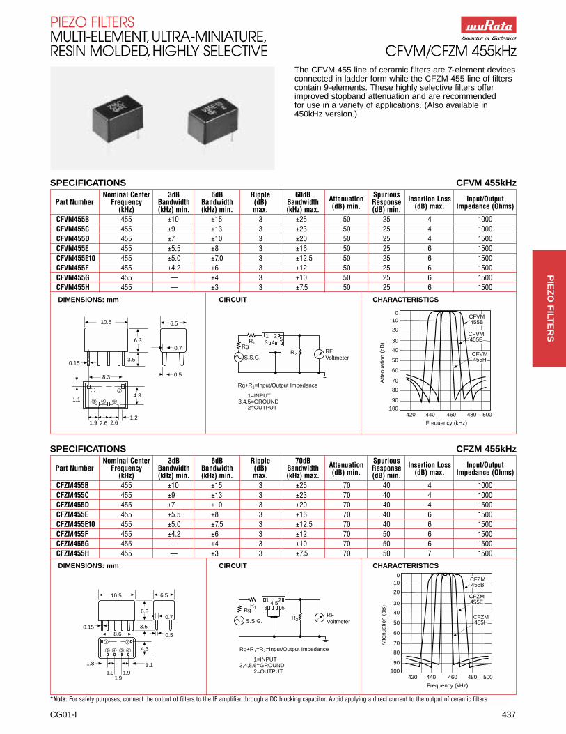
Nominal Center 3dB 6dB Ripple 60dB Attenuation Spurious Insertion Loss Input/OutputPart Number Frequency Bandwidth Bandwidth (dB) Bandwidth (dB) min. Response (dB) max. Impedance (Ohms)(kHz) (kHz) min. (kHz) min. max. (kHz) max. (dB) min.CFVM455B 455 ±10 ±15 3 ±25 50 25 4 1000CFVM455C 455 ±9 ±13 3 ±23 50 25 4 1000CFVM455D 455 ±7 ±10 3 ±20 50 25 4 1500CFVM455E 455 ±5.5 ±8 3 ±16 50 25 6 1500CFVM455E10 455 ±5.0 ±7.0 3 ±12.5 50 25 6 1500CFVM455F 455 ±4.2 ±6 3 ±12 50 25 6 1500CFVM455G 455 — ±4 3 ±10 50 25 6 1500CFVM455H 455 — ±3 3 ±7.5 50 25 6 1500
DIMENSIONS: mm CIRCUIT CHARACTERISTICS
SPECIFICATIONS CFVM 455kHz
CG01-I 437
PIEZO FILTERSMULTI-ELEMENT, ULTRA-MINIATURE,RESIN MOLDED, HIGHLY SELECTIVE CFVM/CFZM 455kHz
The CFVM 455 line of ceramic filters are 7-element devicesconnected in ladder form while the CFZM 455 line of filterscontain 9-elements. These highly selective filters offerimproved stopband attenuation and are recommended for use in a variety of applications. (Also available in 450kHz version.)
Nominal Center 3dB 6dB Ripple 70dB Attenuation Spurious Insertion Loss Input/OutputPart Number Frequency Bandwidth Bandwidth (dB) Bandwidth (dB) min. Response (dB) max. Impedance (Ohms)(kHz) (kHz) min. (kHz) min. max. (kHz) max. (dB) min.CFZM455B 455 ±10 ±15 3 ±25 70 40 4 1000CFZM455C 455 ±9 ±13 3 ±23 70 40 4 1000CFZM455D 455 ±7 ±10 3 ±20 70 40 4 1500CFZM455E 455 ±5.5 ±8 3 ±16 70 40 6 1500CFZM455E10 455 ±5.0 ±7.5 3 ±12.5 70 40 6 1500CFZM455F 455 ±4.2 ±6 3 ±12 70 50 6 1500CFZM455G 455 — ±4 3 ±10 70 50 6 1500CFZM455H 455 — ±3 3 ±7.5 70 50 7 1500
DIMENSIONS: mm CIRCUIT CHARACTERISTICS
SPECIFICATIONS CFZM 455kHz
� �
� � �
1 23 4
5
1 23
4 56
� �
� � � �
10.5
6.3
6.5
0.7
0.5
3.50.15
8.3
1.9 2.6 2.61.2
R1Rg
S.S.G.R2
RFVoltmeter
Rg+R1=Input/Output Impedance
1=INPUT3,4,5=GROUND
2=OUTPUT
Rg+R1=R2=Input/Output Impedance
1=INPUT3,4,5,6=GROUND
2=OUTPUT
R1Rg
S.S.G.R2
RFVoltmeter
420 440 460 480 500
Frequency (kHz)
CFZM455B
CFZM455E
CFZM455H
420 440 460 480 500
Frequency (kHz)
010
20
30
40
50
60
70
80
90
100
CFVM455B
CFVM455E
CFVM455H
Atte
nuat
ion
(dB
)
010
20
30
40
50
60
70
80
90
100
Atte
nuat
ion
(dB
)
10.5
6.3
6.5
0.7
0.5
3.50.158.6
1.91.1
1.91.9
4.3
1.14.3
1.8
*Note: For safety purposes, connect the output of filters to the IF amplifier through a DC blocking capacitor. Avoid applying a direct current to the output of ceramic filters.
PIE
ZO
FILT
ER
S
SPECIFICATIONS CFM/CFJ/CFR/CFS/CFL 455kHz
438 CG01-I
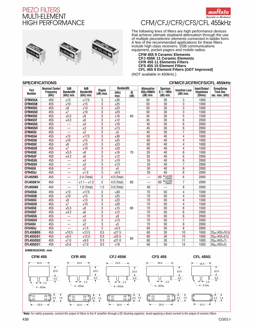
PIEZO FILTERSMULTI-ELEMENTHIGH PERFORMANCE CFM/CFJ/CFR/CFS/CFL 455kHz
The following lines of filters are high performance devicesthat achieve ultimate stopband attenuation through the useof multiple piezoelectric elements connected in ladder form. A few of the recommended applications for these filtersinclude high class receivers. SSB communications equipment, pocket pagers and mobile radios.
CFM 455 9 Ceramic ElementsCFJ 455K 11 Ceramic ElementsCFR 455 11 Elements FiltersCFS 455 15 Element FiltersCFL 455 9 Element Filters (GDT Improved)
(NOT available in 450kHz.)
Part Nominal Center 3dB 6dB RippleBandwidth Attenuation Spurious Insertion Loss Input/Output GroupDelay
Number Frequency Bandwidth Bandwidth (dB) max. (kHz) At 455±100kHz 0.1 ~ 1MHz (dB) max. Impedance Time Dev.(kHz) (kHz) min. (kHz) min. max. (dB) (dB) min. (dB) min. (Ohms) sec. max. (kHz)
CFM455A 455 ±13 ±17.5 3 ±30 50 30 3 1000________________________________________________________ __________________________________________________CFM455B 455 ±10 ±15 3 ±25 50 30 3 1000 ________________________________________________________ __________________________________________________CFM455C 455 ±9 ±13 3 ±23 50 30 3 1000 ________________________________________________________ __________________________________________________CFM455D 455 ±7 ±10 3 ±20 50 30 3 1500 ________________________________________________________ __________________________________________________CFM455E 455 ±5.5 ±8 3 ±16 60 45 30 5 1500 ________________________________________________________ __________________________________________________CFM455F 455 ±4.2 ±6 3 ±12 45 30 6 2000 ________________________________________________________ __________________________________________________CFM455G 455 — ±4 3 ±10 45 30 6 2000 ________________________________________________________ __________________________________________________CFM455H 455 — ±3 3 ±7.5 45 30 6 2000 ________________________________________________________ __________________________________________________CFM455I 455 — ±2 3 ±5 45 30 7 2000 CFR455A 455 ±13 ±17.5 3 ±30 60 40 4 1000 ________________________________________________________ __________________________________________________CFR4558 455 ±10 ±15 3 ±25 60 40 4 1000 ________________________________________________________ __________________________________________________CFR455C 455 ±9 ±13 3 ±23 60 40 4 1000 ________________________________________________________ __________________________________________________CFR455D 455 ±7 ±10 3 ±20 60 40 4 1500 ________________________________________________________ __________________________________________________CFR455E 455 ±5.5 ±8 3 ±16 70 55 40 6 1500 ________________________________________________________ __________________________________________________CFR455F 455 ±4.2 ±6 3 ±12 55 40 6 2000 ________________________________________________________ __________________________________________________CFR455G 455 — ±4 3 ±10 55 40 6 2000 ________________________________________________________ __________________________________________________CFR455H 455 — ±3 3 ±7.5 55 40 7 2000 ________________________________________________________ __________________________________________________CFR455I 455 — ±2 3 ±5 55 40 8 2000 ________________________________________________________ __________________________________________________CFR455J 455 — ±1.5 3 ±4.5 55 40 8 2000 CFJ455K5 455 — 2.4 (Total) 2 4.5 (Total) — 60 6 2000________________________________________________________ __________________________________________________CFJ455K14 455 — ±1.1 ~ ±1.3 2 4.5 (Total) 60 — 60 7 2000________________________________________________________ __________________________________________________CFJ455K8 455 — 1.0 (Total) 1.5 3.0 (Total) 60 — 8 2000 CFS455A 455 ±13 ±17.5 3 ±30 70 50 4 1500 ________________________________________________________ __________________________________________________CFS455B 455 ±10 ±15 3 ±25 70 50 4 1500 ________________________________________________________ __________________________________________________CFS455C 455 ±9 ±13 3 ±23 70 50 4 1500 ________________________________________________________ __________________________________________________CFS455D 455 ±7 ±10 3 ±20 70 50 4 1500 ________________________________________________________ __________________________________________________CFS455E 455 ±5.5 ±8 3 ±15 80 70 50 6 1500 ________________________________________________________ __________________________________________________CFS455F 455 ±4.2 ±6 3 ±12 70 50 6 2000 ________________________________________________________ __________________________________________________CFS455G 455 — ±4 3 ±9 70 50 6 2000 ________________________________________________________ __________________________________________________CFS455H 455 — ±3 3 ±7.5 70 50 7 2000 ________________________________________________________ __________________________________________________CFS455I 455 — ±2 3 ±5 70 50 8 2000 ________________________________________________________ __________________________________________________CFS455J 455 — ±1.5 3 ±4.5 60 50 8 2000CFL455BG5 455 ±10.5 ±13.5 0.5 ±27.5 60 30 10 1000 25� (455±10.5)________________________________________________________CFL455CG1 455 ±9.5 ±12.0 0.5 ±25.5
6060 30 10 1000 35� (455±9.5)________________________________________________________
CFL455DG2 455 ±7.0 ±9.0 0.5 ±21.0 60 30 11 1000 35� (455±7)________________________________________________________CFL455EG1 455 ±5.0 ±7.0 0.5 ±18 60 30 13 1500 30� (455±5)
DIMENSIONS: mm
CFM 455 CFR 455 CFJ 455K CFS 455 CFL 455G
40 at 600~ 700kHz40 at 600~ 700kHz
20.0
20.0 20.0 26.0
23.5 23.5 29.0
10.5 10.5 10.5 10.5
7.5 7.5 7.5 7.5
16.8
4.0 4.0 4.0 4.0
4.04.2 4.0 4.0
1.2 1.2 1.2 1.5 1.5
4–.8Dia. 4–.8Dia. 4–.8Dia. 4–.8Dia. 4–.5 Dia.
(1) (3)(2) (4)
(1) (3)(2) (4)
(1) (3)(2) (4)
(1) (3)(2) (4)
*Note: For safety purposes, connect the output of filters to the IF amplifier through a DC blocking capacitor. Avoid applying a direct current to the output of ceramic filters.
4.0
16.5
10.5
14.2
4.2 7.4

CG01-I 439
PIEZO FILTERSMULTI-ELEMENT, RESIN MOLDED,G.D.T. FLAT TYPE CFWS�Y455kHz
6dB Bandwidth 50dB Bandwidth Insertion LossAttenuation at
Group Delay Time Input /OutputPart Number(kHz) min. (kHz) min. (dB) max.
455 ± 100kHzsec. max. (kHz) Impedance (Ohms)(dB) min.
CFWS455BY ±15.0 ±35 6.0 35 30� (455 ± 10) 1.5k
CFWS455CY ±12.5 ±30 7.0 35 30� (455 ± 8.0) 1.5k
CFWS455DY ±10.0 ±25 8.0 35 30� (455 ± 7.0) 1.5k
CFWS455EY ±7.5 ±20 9.0 35 30� (455 ± 5.0) 1.5k
CFWS455FY ±6.0 ±17.5 10.0 35 40� (455 ± 4.0) 2.0k
CFWS455GY ±4.5 ±15 13.0 35 40� (455 ± 3.0) 2.0k
DIMENSIONS: mm CIRCUIT TYPICAL CHARACTERISTICS
SPECIFICATIONS CFWS�Y 455kHz
(4)
(5)
(1)(2)(3) (4)
(5)
(1)(2)(3)
(1)(2)(5)(3)(4)
7.0
±0.
5
0.8 ± 0.1
7.5
±0.
5
0.6 ± 0.11.2 ±0.5
11.0 ± 0.5
1=INPUT2, 3, 4=OUTPUT
5=GROUND
RgE1
E2S.S.G.0dBm
R1
R2
RF VoltmeterConnection0.15
Sealing
1.5
max
.
2.3 ± 0.5
3.5 ± 0.5
2.0 ± 0.3
2.9 ± 0.32.9 ± 0.3
1.35
±0.
52.6 ± 0.3
4.3 ± 0.3R1+Rg=R2
R2=Input/Output Impedance
The CFWS�Y lines of ceramic filters are 6-element devices connected in ladder form. These highly selective filters aredesigned to address the G.D.T. characteristics required in digital communications. The excellent G.D.T. characteristicsallow these filters to be utilized in areas such as the mobilecellular markets as well as a variety of stereo applications.(Also available in 450kHz version.)
010
20
30
40
50
60
70
80
90
100
200
180
160
140
120
100
80
60
40
20
0420 440 460 480 500
Frequency (kHz)
CFWS455B
CFWS455E
CFWS455B
CFWS455E
Atte
nuat
ion
(dB
)
G.D
.T. T
oler
ance
(�
sec.
)
PIE
ZO
FILT
ER
S
6dB Bandwidth40dB Attenuation at
Insertion Loss Group Delay Time Input /OutputPart Number(kHz) min.
Bandwidth 455 ± 100kHz(dB) max. sec. max. (kHz) Impedance (Ohms)(kHz) max. (dB) min.
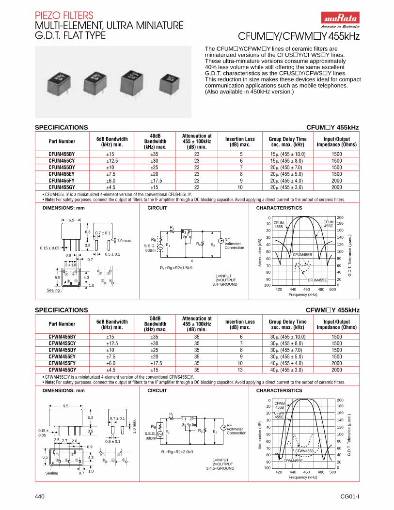
CFUM455BY ±15 ±35 23 5 15� (455 ± 10.0) 1500CFUM455CY ±12.5 ±30 23 6 15� (455 ± 8.0) 1500CFUM455DY ±10 ±25 23 7 20� (455 ± 7.0) 1500CFUM455EY ±7.5 ±20 23 8 20� (455 ± 5.0) 1500CFUM455FY ±6.0 ±17.5 23 9 20� (455 ± 4.0) 2000CFUM455GY ±4.5 ±15 23 10 20� (455 ± 3.0) 2000
• CFUM455�Y is a miniaturized 4-element version of the conventional CFUS455�Y.• Note: For safety purposes, connect the output of filters to the IF amplifier through a DC blocking capacitor. Avoid applying a direct current to the output of ceramic filters.
DIMENSIONS: mm CIRCUIT CHARACTERISTICS
6dB Bandwidth50dB Attenuation at
Insertion Loss Group Delay Time Input /OutputPart Number(kHz) min.
Bandwidth 455 ± 100kHz(dB) max. sec. max. (kHz) Impedance (Ohms)(kHz) max. (dB) min.
CFWM455BY ±15 ±35 35 6 30� (455 ± 10.0) 1500CFWM455CY ±12.5 ±30 35 7 30� (455 ± 8.0) 1500CFWM455DY ±10 ±25 35 8 30� (455 ± 7.0) 1500CFWM455EY ±7.5 ±20 35 9 30� (455 ± 5.0) 1500CFWM455FY ±6.0 ±17.5 35 10 40� (455 ± 4.0) 2000CFWM455GY ±4.5 ±15 35 13 40� (455 ± 3.0) 2000
• CFWM455�Y is a miniaturized 4-element version of the conventional CFWS455�Y.• Note: For safety purposes, connect the output of filters to the IF amplifier through a DC blocking capacitor. Avoid applying a direct current to the output of ceramic filters.
DIMENSIONS: mm CIRCUIT CHARACTERISTICS
SPECIFICATIONS CFUM�Y 455kHz
440 CG01-I
PIEZO FILTERSMULTI-ELEMENT, ULTRA MINIATUREG.D.T. FLAT TYPE CFUM�Y/CFWM�Y455kHz
The CFUM�Y/CFWM�Y lines of ceramic filters are miniaturized versions of the CFUS�Y/CFWS�Y lines. These ultra-miniature versions consume approximately 40% less volume while still offering the same excellent G.D.T. characteristics as the CFUS�Y/CFWS�Y lines. This reduction in size makes these devices ideal for compact communication applications such as mobile telephones.(Also available in 450kHz version.)
� �
� �
� �
� �
6.5
6.3
3.5
1.82.4
0.15 ± 0.05
Sealing
4.36.5
1.0
0.80.7
0.7 ± 0.1
1.0 max.
0.5 ± 0.1
R1+Rg=R2=1.5k�
1=INPUT2=OUTPUT
3,4=GROUND
S.S.G.0dBm
Rg
R1
R2 E2E1
123
4
0
10
20
30
40
50
60
70
80
90
100
200
180
160
140
120
100
80
60
40
20
0420 440 460 480 500
Frequency (kHz)
CFUM455B
CFUM455E
CFUM455B
CFUM455E
Atte
nuat
ion
(dB
)
G.D
.T. T
oler
ance
(�
sec.
)
RF VoltmeterConnection
R1+Rg=R2=2.0k�
1=INPUT2=OUTPUT
3,4,5=GROUND
S.S.G.0dBm
Rg
R1
R2 E2E1
1 2
3 4 5 RF VoltmeterConnection
SPECIFICATIONS CFWM�Y 455kHz
��
� � �
��
� � �
9.5
6.3
3.5
2.82.5
6.5
0.15 ±0.05
Sealing
4.3
1.0
0.9
2.7
0.7
0.7 ± 0.1
1.0
max
.
0.5 ± 0.1
0
10
20
30
40
50
60
70
80
90
100
200
180
160
140
120
100
80
60
40
20
0420 440 460 480 500
Frequency (kHz)
CFWM455B
CFWM455E
CFWM455B
CFWM455E
Atte
nuat
ion
(dB
)
G.D
.T. T
oler
ance
(�
sec.
)

Nominal 3dB 6dB 50dB Spurious Insertion G.D.T. Input/OutputPart Number Center Bandwidth Bandwidth Bandwidth Response Loss Ripple Deviation Impedance
Frequency (kHz min.) (kHz min.) (kHz min.) Attenuation (dB max.) (dB max.) (�sec. max.) (Ohms)(kHz) (dB min.)
CFUXC450A100H-TC01 450 — ±17.5 ±55 40 5 0.5 15 2k
CFUXC450B100H-TC01 450 — ±15 ±50 40 6 0.5 15 2k
CFUXC450C100H-TC01 450 ±9 ~ ±12 — ±35 40 6 0.5 27 2k
DIMENSIONS: mm TEST CIRCUIT
TAPING DIMENSIONS: mm REEL DIMENSIONS: mm
SPECIFICATIONS CFUXC 450kHz
CG01-I 441
PIEZO FILTERSSURFACE MOUNTED CHIP PIEZOELECTRIC CERAMICS FILTERSFOR MOBILE COMMUNICATIONS APPLICATIONS CFUXC 450kHz
Introducing Murata’s newest surface mount kHz filter, theCFUXC Series. This is a 4-element filter that uses new tech-nology developed by Murata to achieve the world’s smallestand lightest surface mount kHz filter. This 2mm high filteroffers the attenuation of a 6-element filter and a good G.D.T.in a smaller package.
*Note: For safety purposes, connect the output of filters to the IF amplifier through a DC blocking capacitor. Avoid applying a direct current to the output of ceramic filters.
NEW
E2R2E1
R1
Rg
S.S.G.0dBm
� ��
� ��
5 0 C
*M
1.90.5
(5.8) (5.5)
1.25 ± 0.3
3.25 ± 0.3
5.25 ± 0.3
6–1.5 ± 0.2
6–1.0
6–0.6
� � �
� � �
0.3R0.15
1.0
1.0Dot Marking
6.5 ± 0.3
6.5 ± 0.3
� � �
� � �
R1 + Rg = R2 = 2.0k�
Insertion Loss (dB) = 20 • logE1 – 6 (dB)(E2)
= 20 • log E1 – 20 • log E2 – 6 (dB)
E1: S.S.G. high impedance output
�: Input�: Output
����: Ground
Tolerance: ±0.1mm
*: EIA-J Date Code
2.0 ± 0.2
�13.0 ± 0.2(�100) (�330)
17.5 ± 1.0
22.9 max.
MMM M
2.1 ± 0.1
6.9
± 0.
1
16.0
± 0
.2
7.5
± 0.
1
1.75 ± 0.1
4.0 ± 0.12.0 ± 0.1
�1.5 +0.1–0.0
8.0 ± 0.1
6.9 ± 0.1 Cover Tape
Feeding Direction
PIE
ZO
FILT
ER
S

Center Frequency Bandwidth (Total) Ripple (max.) *Insertion Stop Band Group Delay (max.) Source____________________________________________________________ _________________Part
Nom. Tol. 3dB (min.) 6dB (min.) 40dB (max.) Point of Loss Atten. (min.)
Point of And Load
Number(kHz) ± (kHz) (kHz) (kHz) (kHz) dB Measure
(max.) at ± 100kHz �S MeasureImpedance
dB dB (Ohms)
CFUCG455E-TC 455 1.5 — 15 30 1.5 — 6 27 — — 1500CFUCG455F-TC 455 1.5 — 12 25 1.5 — 6 27 — — 1500CFUCG455G-TC 455 1 — 9 20 1.5 — 6 25 — — 1500CFUCG455FX-TC 455 1.5 — 12 30 1 — 6 27 25 — 1500CFUCG455GX-TC 455 1 — 9 25 1 — 6 25 25 — 1500CFUCG455HX-TC 455 1 — 6 20 1 — 7 25 25 — 1500SFGCG455AX-TC 455 2.0 — 35 80 1 — 4 25 15 — 1000SFGCG455BX-TC 455 1.5 — 30 70 1 — 5 25 15 — 1000SFGCG455CX-TC 455 1.5 — 25 60 1 — 6 25 15 — 1000SFGCG455DX-TC 455 1 — 20 50 1 — 7 23 20 — 1500SFGCG455EX-TC 455 1 — 15 40 1 — 8 23 20 — 1500SFPC455E-TC01 455 1.5 — 15 30 — — 6 27 — — 1500SFPC455F-TC01 455 1.5 — 12 25 — — 6 27 — — 1500SFPC455G-TC01 455 1 — 9 20 — — 6 25 — — 1500SFPC455H-TC01 455 1 — 6 18 — — 6 25 — — 2000CFWC455CZ-TC 455 — 21 to 26 — — 0.5 ±10.5 6 50 27 ±10.5 1000CFWC455CZ2-TC 455 — 18 to 22 — — 0.5 ±9 6 50 27 ±9 1000
DIMENSIONS: mm SFPCCFUCG/SFGCG
� � �
PRELIMINARY SPECIFICATIONS SMD 455kHz
*Note: For safety purposes, connect the output of filters to the IF amplifier through a DC blocking capacitor. Avoid applying a direct current to the output of ceramic filters.
442 CG01-I
PIEZO FILTERSSURFACE MOUNTED CHIP PIEZOELECTRIC CERAMICS FILTERSFOR AM APPLICATIONS CFUCG, SFGCG, SFPC, CFWC 455kHz
Along with the development of the AM chip filter, IF filtersfor AM radios have also been made smaller, thinner and ina chip configuration for surface mounting. This is one moreexample of Murata Electronics’ leadership in convertingconventional electronic components to chip technology.
� ��6.5
1.04.0 3.01.0
1.5 1.56.0
1.0 ± 0.1 1.0 ± 0.1 1.2 ± 0.1
0.9 ± 0.1
Sealing
CO.5
Sealing
7.5max. 4.0
max.
�: INPUT�: OUTPUT�: GROUND
7.0
5 0 D
*7.5
3.0
1.5 1.5 1.62.02.0
8.4max. 5.0 max.
Sealing
M
SPECIFICATIONS
CFWC TEST CIRCUIT
�: INPUT�: OUTPUT
� �: GROUNDBody Color: CreamTolerance without notice: ±0.3 mm
(in mm)
Sealing
Sealing
7.5 max.6.5
1.2 ± 0.1
3.0 5.5 3.0
11.5
1.5 ± 0.35.5 3.0
1.2 ± 0.1 1.2 ± 0.11.2 ± 0.1
1.5 ± 0.3
3.0 max.
C0.3
Input Marking
Rg + R1 = Input/Output Impedance
CFWC455 Series
R.F.VoltmeterE2
R1
Rg R2S.S.G.0 dBm
E1
Connection�: INPUT�: OUTPUT
� �: GROUND
E 4
*M
* : EIA-J Monthly Code
•

PIEZO FILTERSSURFACE MOUNTED CHIP PIEZOELECTRIC CERAMIC FILTERSFOR AM APPLICATIONS SFGCG, SFPC, CFUCG, CFWC 455kHz
CG01-I 443
CHARACTERISTICS (TYP.)
PAD DIMENSIONS: mm
PLASTIC TAPE DIMENSIONS: mm
SFGCG455BX
405 455 505
Frequency (kHz)
Atte
nuat
ion
(dB
)
G.D
.T. (
�se
c.)
Atte
nuat
ion
(dB
)
445 455 465
Frequency (kHz)
400
300
200
100
0
0
4
8
12
16
20
24
28
32
36
40
200
100
0
0
10
20
30
40
50
60
70
80
90
100
CFWC455E4
SFPC SFGCG/CFUCG CFWC
SFPC – TC01 REEL
SFGCG/CFUCG – TC REEL
CFWC – TC REEL
6.95
1.2 1.40.7 0.7 11.5
1.2
2.0
2.0
3.5
3.0
1.8
0.75
1.55
2.3
5.5
GNDIN OUT
4-R3.0GND
3.0
7.5 max.6.5
2.475 2.0
1.1
0.925 2.00.9
1.55
7.45
1.6
0.8
2.0
4.0 ± 0.1
2.0 ± 0.1
12.0 ± 0.17.8 ± 0.1
2.2 ± 0.213.0 ± 0.2
17.5 ± 1.0
7.4 ± 0.1
Covering Tape 5.3 ± 0.1
8.8 ± 0.17.5
±0.
16.
75 ±
0.1 9.2
±0.
1
16.0
±0.
3
1.75
±0.
1
(�33
0)
�1.5 –0.1+0.0
(�80
)
2.0 ± 0.1
8.0 ± 0.16.7 ± 0.1
2.0 ± 0.213.0 ± 0.5
22.5 max.17.5 ± 0.5
6.3 ± 0.1
Covering TapeDirection of Feed
4.2 ± 0.1
7.7 ± 0.1
7.5
±0.
1
6.75 ±
0.1 8.1
±0.
1
16.0
±0.
2
1.75
±0.
1
(�17
8)
�1.5 –0.1+0.0
(�80
)
4.0 ± 0.12.0 ± 0.1
12.0 ± 0.1 8.1 ± 0.1
2.0 ± 0.213.0 ± 0.5
25.5 ± 0.530.5 max.
7.7 ± 0.1
Covering Tape
Direction of Feed
3.2 ± 0.1
12.0 ± 0.1
0.4 ± 0.1
11.5
±0.
1
12.4
±0.
1
24.0
±0.
3
1.75
±0.
1
(�17
8)
�1.5 –0.1+0.0
(�62
)
G.D
.T. (
�se
c.)
4.0 ± 0.1
1.2
22.9 max.
PIE
ZO
FILT
ER
S
Recovered Audio DistortionPart Number/
3dB Bandwidth Output (at 455kHz) within IC ApplicationCharacteristics(from 544kHz) min. (at 455kHz) max. 455 ± 8kHz
CDB455C7 ±4.0 340 ± 60mV 2.5% — Cordless Telephone,CDBM455C7 ±4.0 340 ± 60mV 3.0% — MC3357 Communications
CDBC455CX7 ±4.0 350 ± 60mV 3.0% — Equipment
CDB455C9 ±5.0 100mV min. 1.5% —
CDBM455C9 ±5.0 100mV min. 1.5% — Cordless Telephone,
CDBC455CX9 ±4.0 120 ± 40mV 1.5% — NE604N Cellular Phone,
CDB455CL9 ±15.0 70 ± 20mV 1.5% 3.5% max.Communications
CDBM455CL9 ±15.0 70 ± 20mV 1.5% 3.5% max.Equipment
CDB455C13A ±4.0 350 ± 50mV 3.0% —
CDBM455C13A ±4.0 350 ± 50mV 3.0% —Cellular Phone,CDBC455CX13 ±4.0 330 ± 50mV 4.0% —
CXA1003BM CommunicationsCDB455CL13 ±15.0 110 ± 30mV 1.5% 5.0% max. EquipmentCDBM455CL13 ±15.0 110 ± 30mV 1.5% 5.0% max.
CDBC455CLX13 ±13.0 120 ± 30mV 1.5% 5.0% max.
Cellular Phone,CDB455C16 ±4.0 185 ± 40mV 2.0% —
MC3372Cordless Telephone,
CDBM455C16 ±4.0 185 ± 40mV 2.0% —Communications
CDBC455CX16 ±4.0 175 ± 40mV 2.0% — Equipment
Cordless Telephone,CDBM455C18 ±3.0 180 ± 40mV 2.0% — MC3371 Communications
Equipment
CDB455C21 ±4.0 55 ± 20mV 2.0% —
CDBM455C21 ±4.0 55 ± 20mV 2.0% —Cordless Telephone,
CDBC455CX21 ±4.0 55 ± 20mV 2.0% —TA31132 Cellular Phone,
CDB455CL21 ±13.0 65 ± 20mV 2.5% 5.0% max. Communications
CDBM455CL21 ±13.0 65 ± 20mV 2.5% 5.0% max. Equipment
CDBC455CLX21 ±11.0 75 ± 25mV 2.5% 5.0% max.
CDB455C24 ±4.0 100 ± 40mV 2.0% — Cordless Telephone,CDBM455C24 ±4.0 100 ± 40mV 2.0% — TA31136 Communications
CDBC455CX24 ±4.0 100 ± 40mV 2.0% — Equipment
CDB455C27 ±4.0 100 ± 40mV 2.0% — Cordless Telephone,CDBM455C27 ±4.0 100 ± 40mV 2.0% — TK10487 Communications
CDBC455CX27 ±4.0 90 ± 30mV 2.0% — Equipment
CDB455C28 ±4.0 40 ± 20mV 3.0% —
CDBM455C28 ±4.0 40 ± 20mV 3.0% — TA31142 Pager
CDBC455CX28 ±4.0 40 ± 20mV 3.0% —
PIEZO FILTERSHIGH PERFORMANCE CERAMIC DISCRIMINATORSFOR MOBILE COMMUNICATION EQUIPMENT CDB/CDBC/CDBM 455kHz
444 CG01-I
RECOVERED AUDIO CURVE SPECIFICATIONS CDB/CDBC/CDBM 455kHz
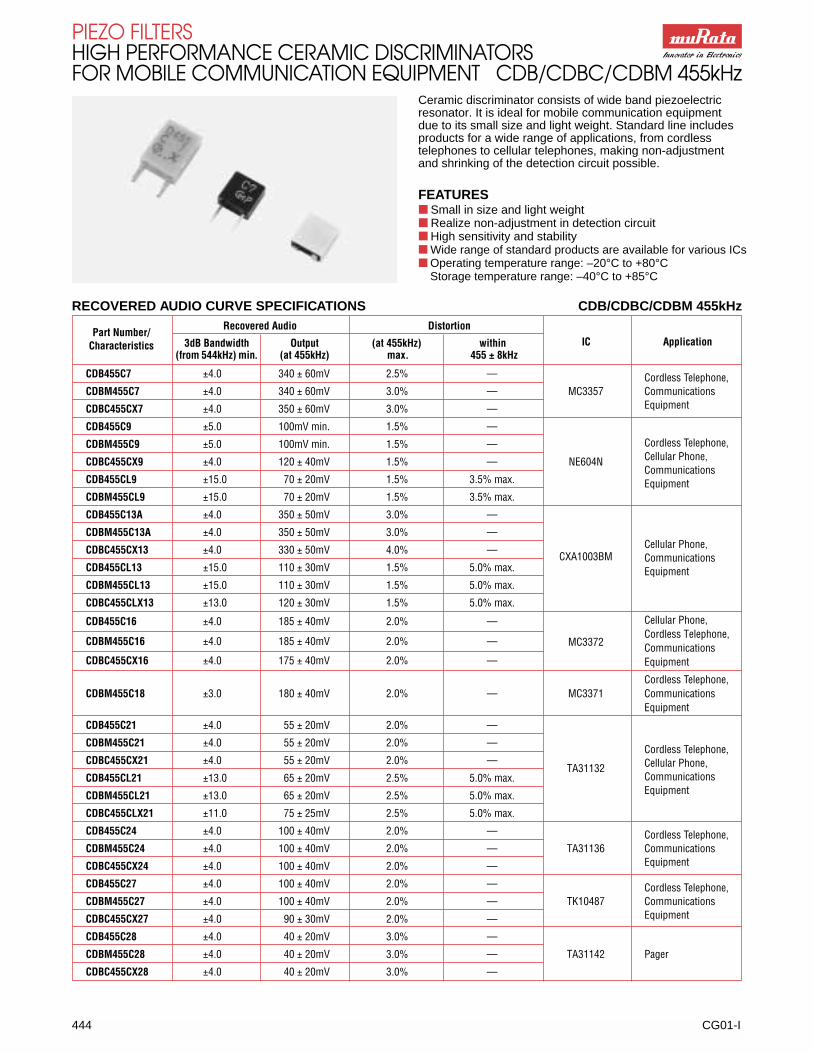
Ceramic discriminator consists of wide band piezoelectric resonator. It is ideal for mobile communication equipment due to its small size and light weight. Standard line includesproducts for a wide range of applications, from cordless telephones to cellular telephones, making non-adjustment and shrinking of the detection circuit possible.
FEATURES■ Small in size and light weight■ Realize non-adjustment in detection circuit■ High sensitivity and stability■ Wide range of standard products are available for various ICs■ Operating temperature range: –20°C to +80°C
Storage temperature range: –40°C to +85°C

Recovered Audio DistortionPart Number/
3dB Bandwidth Output (at 455kHz) within IC ApplicationCharacteristics(from 455kHz) min. (at 455kHz) max. 455 ± 8kHz
CDB455C29 ±4.0 125 ± 30mV 2.5% — Cordless Telephone,CDBM455C29 ±4.0 125 ± 30mV 2.5% — NE605 Communications
CDBC455CX29 ±4.0 100 ± 30mV 2.5% — Equipment
CDB455C30 ±4.0 90 ± 30mV 2.0% — Telephone,CDBM455C30 ±4.0 90 ± 30mV 2.0% — TK14501 Communications
CDBC455CX30 ±4.0 80 ± 20mV 2.0% — Equipment
CDB455C32 ±4.0 40 ± 20mV 3.0% —
CDBM455C32 ±4.0 40 ± 20mV 3.0% — TA31143 Pager
CDBC455CX32 ±4.0 40 ± 20mV 3.0% —
CDB455C34 ±4.0 65 ± 20mV 2.5% — Cordless Telephone,
CDBM455C34 ±4.0 65 ± 20mV 2.5% —MC13136 Communications
Equipment
CDB455C35 ±4.0 100 ± 40mV 2.5% — Cordless Telephone,CDBM455C35 ±4.0 100 ± 40mV 2.5% — TK10930 Communications
CDBC455CX35 ±4.0 100 ± 40mV 2.5% — Equipment
CDBM455C36 ±3.5 100 ± 25mV 3.5% — NE(SA)606, Cordless Telephone,CDBC455CLX36 ±13.0 90 ± 30mV 2.5% 5.0% max. NE(SA)616 Cellular Phone
CDBM455C39 ±4.0 85 ± 20mV 2.5% —NE(SA)607/617 Cordless Telephone
CDBC455CLX39 ±11.0 130 ± 20mV 2.5% 7.0% max.
CDBM455C40 ±4.0 40 ± 20mV 3.0% —TA31145 Pager
CDBC455CX40 ±4.0 40 ± 20mV 3.5% —
CDB455C42 ±4.0 40 ± 15mV 3.0% — TK14590, PagerCDBM455C42 ±4.0 40 ± 15mV 3.0% — TK14591
CDBM455C49 ±4.0 45 ± 10mV 3.0% —MC3361 Cordless Telephone
CDBC455CX49 ±4.0 45 ± 10mV 3.0% —
CDBM455C50 ±4.0 64 ± 6.4mV 4.0% —CXA3117 Pager
CDBC455CX50 ±4.0 64 ± 6.4mV 4.0% —
CDBC455C52 ±3.0 65 ± 25mV 3.0% — SA625CommunicationsEquipment
CDBC455C55 ±3.0 40 ± 15mV 3.0% — SA608DCommunicationsEquipment
CDBC455C56 ±4.0 100 ± 20mV 2.0% — BA4116FVCommunicationsEquipment
PIEZO FILTERSHIGH PERFORMANCE CERAMIC DISCRIMINATORSFOR MOBILE COMMUNICATION EQUIPMENT CDB/CDBC/CDBM 455kHz
CG01-I 445
RECOVERED AUDIO CURVE SPECIFICATIONS CDB/CDBC/CDBM 455kHz
Part Number/ Resonant Antiresonant ∆F (Fa-Fr) Resonant Capacitance IC ApplicationCharacteristics Frequency (Fr) Frequency (Fa) Resistance (R1) (C)
CDBM455C2 447 ± 1.5kHz (|Z•| = 2.05k�) 463 ± 1.5kHz (|Z
•| = 10.0k�) 140pF ± 20%
TA8104F PagerCDBC455CX2 447 ± 1.5kHz (|Z
•| = 0.80k�) 463 ± 1.5kHz (|Z
•| = 3.65k�) 280pF ± 20%
CDB455C3 — 455 ± 1.5kHz 48 ± 5.0kHz 70� max. 600pF ± 20%CXA1184M Pager
CDBM455C3 — 455 ± 1.5kHz 46 ± 5.0kHz 70� max. 550pF ± 20%
CDBM455C4 — 470 ± 1.0kHz 43 ± 2.0kHz 300� max. 140pF ± 20% LA8610 Pager
CDB455C10 429 ± 2kHz — 51 ± 5.0kHz 70� max. 580pF ± 20%TA8103F Cordless Telephone
CDBM455C10 429 ± 2kHz — 51 ± 5.0kHz 70� max. 580pF ± 20%
CDBM455C15 — 463.5 ± 1kHz 43 ± 2.0kHz 300� max. 140pF ± 20% CXA1183M Cordless Telephone
CDBM455C25 — 465 ± 1.5kHz 45 ± 4.0kHz 300� max. 135pF ± 20% CXA1484 Pager
CDBM455C31 447 ± 1.5kHz (|Z•| = 2.05k�) 463 ± 1.5kHz (|Z
•| = 10.0k�) 140pF ± 20%
TA31141 PagerCDBC455CX31 447 ± 1.5kHz (|Z
•| = 0.80k�) 463 ± 1.5kHz (|Z
•| = 3.65k�) 280pF ± 20%
CDBM455C33 — 465 ± 1.5kHz 45 ± 4.0kHz 300� max. 135pF ± 20% CXA1474 Pager
IMPEDANCE CURVE SPECIFICATIONS CDB/CDBC/CDBM 455kHz
PIE
ZO
FILT
ER
S

PIEZO FILTERSHIGH PERFORMANCE CERAMIC DISCRIMINATORSFOR MOBILE COMMUNICATION EQUIPMENT CDB/CDBC/CDBM 455kHz
446 CG01-I
DIMENSIONS: mm
PLASTIC TAPE DIMENSIONS: mm
CDB455C� /CDB455CL�
3.5
±0.
39.
0 ±
0.3
0.1
±0.
05
0.25
±0.
05
3.5
±0.
5
1.75 ± 0.5
1.5 max.
0.8 ± 0.1
Applicable Part Number: All Applicable Part Number: 3, 7, 9, 10, 13, 21, 24, 27, 28, 29, 30, 32, 34, 35, 40, 42, 47, 49, 50
1.1 ± 0.1
Sealing
7.0 ± 0.3
5.0 ± 0.2
CDBM455C� /CDBM455CL�
3.0 ± 0.3
6.0
max
.
6.3
max
.
4.2 ± 0.5
1.0 ± 0.3
0.5
±0.
2
1.5
±0.
3
0.15 ± 0.050.5 ± 0.1
0.9 ± 0.2
6.0 ± 0.2
4.2 ± 0.2
CDBM455C�
6.0
max
.
6.3
max
.
0.6 ± 0.2
1.8 ± 0.2
4.2 ± 0.50.15 ± 0.05
0.9 ± 0.2
Applicable Part Number: 2, 4, 15, 16, 18, 25, 31, 33, 36, 39 Applicable Part Number: All
3.0 ± 0.3
6.0 ± 0.2
4.2 ± 0.2
0.5 ± 0.1
CDBC455CX� /CDBC455CLX�
3.1
max
.Sealing
2.0
1.2 1.22.5
Standard Land Dimension
1.15 ± 0.23.7 ± 0.2
6.0 ± 0.2
1.0 ± 0.1
6.6
±0.
3
6.2
±0.
2
1.5 ± 0.3
CDBC455C� – TC
The marked part number is faced on the cover tape side.
Reel
M
50C56
* M
50C56
* M
50C56
* M
50C56
* M
50C56
*M
50C56
*
2.0 ± 0.14.0 ± 0.1
8.0 ± 0.1Feeding Direction
1.75
± 0
.17.
5 ±
0.1
16.0
± 0
.15
3.3 ± 0.1
7.2
± 0.
1
3° max.3° max. Cover Tape
6.3 ± 0.1
�1.5 +1.0–0
22.5 max.
18.5 +0.3–0
(�80
)
(�17
8)
2.0 ± 0.2
�13.0 ± 0.5

Part Number Center Freq. (MHz) 3dB Bandwidth (kHz) Insertion Loss (dB max.) Terminal Impedance (Ohms)SFE10.7MFP1 10.7 (Nominal) Fn ±5 min. Fn ±35 max. 6 470
DIMENSIONS: mm CIRCUIT
SPECIFICATIONS SFE 10.7
Part Number Resonant Frequency (kHz) Resonant Resistance (Ohms) �f (fa-fr) (kHz)BFU450K3 450 ± 1 30 27.5 ± 4.5BFU450C 450 ± 1 20 14 ± 2BFU450C4N 450 ± 0.8 30 9 ± 2• Temperature Coefficient is typically 10ppm/°C
Part Number Center Frequency (kHz) 3dB Bandwidth (kHz) SelectivityBFU455K 455 ± 2 8 ± 2 8dB @ f0=–9, 12dB @ f0=+9
DIMENSIONS: mm DIMENSIONS: mm CIRCUIT
SPECIFICATIONS BFU 450/455
CG01-I 447
PIEZO FILTERSCERAMIC FILTERS FOR SIGNAL DETECTION
SFE & BFU SeriesThe following filters were specifically designed for signaldetection circuitry used in applications such as that foundin the search-stop functions of electronically tuned radios.
1.1 ± 0.1
2.5 ± 0.2 2.5 ± 0.2
0.6 ± 0.1
1.3 ± 0.1
0.3 ± 0.15.0 ± 1.0
1.8 ± 0.2
0.6 ± 0.210.0 ± 2.0
10.0 ± 2.03.5 +1.5
–1.0
1.5 max.
7.0 ± 0.3 3.5 ± 0.3
9.0 ± 0.3
3.5 ± 0.5
5.0 ± 0.25.0 ± 0.2Sealing
1.1 ± 0.1
1.75 ± 0.50.8±0.1
0.35
0.35
0.1
2–1.0
1.5 max.
7.0 ± 0.3 3.5 ± 0.3
9.0 ± 0.3
3.5 ± 0.5
5.0 ± 0.25.0 ± 0.2Sealing
1.1 ± 0.1
1.75 ± 0.5
0.8±0.1
1.1 ± 0.1
2–1.0 D.
S.S.G.
Rg=50�
R1+Rg=R2=Input/Output Impedance C=10pF±2pF (including stray capacitance
and input capacitance of RF Voltmeter.)
1=INPUT2=GROUND3=OUTPUT
RFVoltmeter
S.S.G.
BFU450C4N
BFU450K3/C/C4NBFU450K3/C/C4N
BFU455K
BFU455K
BFU450C4N
BFU455k
5k
3k
3k15k - 20k
2SC4030.01�
0.01�
0.01�
1k
For Fr and R1
Emitter current = 1.0mA
For Fa
3k�
50k� 50k�
3�
S.S.G.
S.S.G.0.01VConst.
RFVoltmeter
RFVoltmeter
RFVoltmeter
R1
R2 C
1
2
3
(3)
(2)
(1)
+6V
PIE
ZO
FILT
ER
S
448 CG01-I
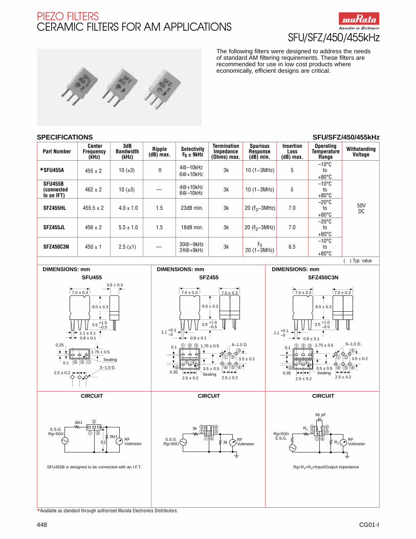
PIEZO FILTERSCERAMIC FILTERS FOR AM APPLICATIONS
SFU/SFZ/450/455kHzThe following filters were designed to address the needs of standard AM filtering requirements. These filters are recommended for use in low cost products where economically, efficient designs are critical.
SPECIFICATIONS SFU/SFZ/450/455kHzCenter 3dB Ripple Selectivity Termination Spurious Insertion Operating WithstandingPart Number Frequency Bandwidth (dB) max. F0 ± 9kHz Impedance Response Loss Temperature Voltage(kHz) (kHz) (Ohms) max. (dB) min. (dB) max. Range
–10°C�SFU455A 455 ± 2 10 (±3) 0 4@–10kHz 3k 10 (1~3MHz) 5 to
6@+10kHz +80°CSFU455B
4@+10kHz–10°C
(connected 462 ± 2 10 (±3) —6@–10kHz
3k 10 (1~3MHz) 5 toto an IFT) +80°C
–20°C50VSFZ455HL 455.5 ± 2 4.0 ± 1.0 1.5 23dB min. 3k 20 (F0~3MHz) 7.0 toDC
+80°C–20°C
SFZ455JL 456 ± 2 5.5 ± 1.0 1.5 18dB min. 3k 20 (F0~3MHz) 7.0 to+80°C–10°C
SFZ450C3N 450 ± 1 2.5 (±1) — 30@–9kHz 3k F0 6.5 to24@+9kHz 20 (1~3MHz)
+80°C( ) Typ. value
DIMENSIONS: mm DIMENSIONS: mm DIMENSIONS: mm
SFU455 SFZ455 SFZ450C3N
CIRCUIT CIRCUIT CIRCUIT
���
�
� �
� ��
� � �
� �
�
� � �
� �
��
��
� �
�
� � �
� �
��
��
� � �
� ��
7.0 ± 0.3
3.5 ± 0.3
9.0 ± 0.3
1.1 ± 0.10.8 ± 0.1
0.25
0.1
1.75 ± 0.5
Sealing
3–1.0 D.2.5 ± 0.2
7.0 ± 0.3
9.0 ± 0.3
0.8 ± 0.1
1.75 ± 0.5
2.5 ± 0.2Sealing
1.1 +0.1–0
7.0 ± 0.3
6–1.0 D.
3.5 ± 0.2
2.5 ± 0.2
3k�
3k�RFVoltmeterE2
S.S.G.Rg=50�
3k
3kRFVoltmeter
S.S.G.Rg=50�
R1
RFVoltmeter
Rg=50�S.S.G.
56 pF
R2
Rg+R1=R2=Input/Output ImpedanceSFU455B is designed to be connected with an I.F.T.
7.0 ± 0.3
9.0 ± 0.3
0.8 ± 0.1
1.75 ± 0.5
2.5 ± 0.2Sealing
1.1 +0.1–0
3.5 +1.0–0.5
3.5 +1.0–0.5
3.5 +1.0–0.5
7.0 ± 0.3
6–1.0 D.
3.5 ± 0.2
2.5 ± 0.20.35
0.1
3.5 ± 0.50.35
�Available as standard through authorized Murata Electronics Distributors.
3.5 ± 0.5
0.1
PIEZO FILTERSCERAMIC FILTERSMHz SERIES
CG01-I 449
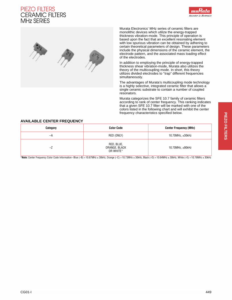
Murata Electronics’ MHz series of ceramic filters are monolithic devices which utilize the energy-trapped thickness vibration-mode. This principle of operation isbased upon the fact that an excellent resonating elementwith low spurious vibration can be obtained by adhering tocertain theoretical parameters of design. These parametersinclude the physical dimensions of the ceramic element, the electrode pattern, and the associated mass loading effect of the electrodes.
In addition to employing the principle of energy-trappedthickness shear vibration-mode, Murata also utilizes the theory of the multicoupling mode. In short, this theory utilizes divided electrodes to “trap” different frequenciessimultaneously.
The advantages of Murata’s multicoupling mode technologyis a highly selective, integrated ceramic filter that allows asingle ceramic substrate to contain a number of coupled resonators.
Murata categorizes the SFE 10.7 family of ceramic filtersaccording to rank of center frequency. This ranking indicatesthat a given SFE 10.7 filter will be marked with one of thecolors listed in the following chart and will exhibit the centerfrequency characteristics specified below.
Category Color Code Center Frequency (MHz)
–A RED (ONLY) 10.70MHz, ±30kHz
RED, BLUE,–Z ORANGE, BLACK 10.70MHz, ±90kHz
OR WHITE*
AVAILABLE CENTER FREQUENCY
*Note: Center Frequency Color Code Information–Blue (–B) = 10.67MHz ± 30kHz, Orange (–C) = 10.73MHz ± 30kHz, Black (–D) = 10.64MHz ± 30kHz, White (–E) = 10.76MHz ± 30kHz
PIE
ZO
FILT
ER
S

Part Number 3dB Bandwidth 20dB Bandwidth Ripple Insertion Loss Spurious (9 ~ 12MHz)(kHz) (kHz) max. (dB) max. (dB) max. (dB) min.
SFE10.7MA5-A 280 ± 50 650 (520) 1 6 (4) 30 (43)FM-IF SFE10.7MS2-A 230 ± 50 600 (420) 1 6 (4) 40 (45)
SFE10.7MS3-A 180 ± 40 520 (380) 1 7 (4.5) 40 (45)• Input/output impedance: 330� ( ) Typ. value
SFE10.7MA5A10-A 280 ± 50 590 (480) 1 2.5 ± 2.0 30 (42)
A10 Series SFE10.7MS2A10-A 230 ± 50 520 (400) 1 3.0 ± 2.0 35 (43)SFE10.7MS3A10-A 180 ± 40 470 (360) 1 3.5 ± 1.5 35 (43)SFE10.7MJA10-A 150 ± 30 360 (290) 1 4.5 ± 2.0 35 (44)
• Input/output impedance: 330� • Low loss and high selectivity. ( ) Typ. value
SFE10.7MA5B10-A 280 ± 50 650 1 3.0 ± 2.0 45B10 Series SFE10.7MS2B10-A 230 ± 50 570 1 3.0 ± 2.0 45
SFE10.7MS3B10-A 180 ± 40 520 1 5.0 ± 2.0 45• Input/output impedance: 330� • High attenuation type
SFE10.7MA5C10-A 280 ± 50 650 (540) 1 3.0 ± 2.0 30 (47)SFE10.7MS2C10-A 230 ± 50 570 (470) 1 3.0 ± 2.0 40 (48)
C10 Series SFE10.7MS3C10-A 180 ± 40 470 (360) 1 3.5 ± 2.0 35 (45)SFE10.7MJC10-A 150 ± 40 360 (300) 1 4.5 ± 2.0 35 (48)SFE10.7MHC10-A 110 ± 30 350 (260) 1 7.0 ± 2.0 30 (42)
• Input/output impedance: 330� • Most suitable for a thin type and low profile set. • The performance is the same as that of conventional types. ( ) Typ. value
MA5 Series MA5A10 Series MA5C10 Series CIRCUIT
SFE10.7MA5-A SFE10.7MS2-A SFE10.7MS3-A SFE10.7MJA10-A
FREQUENCY CHARACTERISTICS
450 CG01-I
PIEZO FILTERSCERAMIC FILTERS LOW LOSS,HIGHLY SELECTIVE, MINIATURE SFE MA/MS/MJ/MH 10.7MHz
The standard SFE 10.7 line of ceramic filters are extremely reliable devices that exhibit excellent waveform symmetry.These filters have traditionally found wide application in FM receiver technology.
10.5 10.6 10.7 10.8 10.9Frequency (MHz)
Atte
nuat
ion
(dB
)
01
2
3
4
5
67
8.7 9.7 10.7 11.7 12.7Frequency (MHz)
Atte
nuat
ion
(dB
)
01020
30
40506070
Gro
up D
elay
Tim
e (�
sec.
)1.21.0
0.80.60.4
0.2
0
10.5 10.6 10.7 10.8 10.9Frequency (MHz)
Atte
nuat
ion
(dB
)
01
2
3
4
5
67
8.7 9.7 10.7 11.7 12.7Frequency (MHz)
Atte
nuat
ion
(dB
)
010203040506070
Gro
up D
elay
Tim
e (�
sec.
)1.21.0
0.8
0.6
0.4
0.20
10.5 10.6 10.7 10.8 10.9Frequency (MHz)
Atte
nuat
ion
(dB
)
01
2
3
4
5
67
8.7 9.7 10.7 11.7 12.7Frequency (MHz)
Atte
nuat
ion
(dB
)
010
203040506070
Gro
up D
elay
Tim
e (�
sec.
)1.21.0
0.8
0.6
0.4
0.2
0
10.5 10.6 10.7 10.8 10.9Frequency (MHz)
Atte
nuat
ion
(dB
)
01
2
34
5
67
8.7 9.7 10.7 11.7 12.7Frequency (MHz)
Atte
nuat
ion
(dB
)
0102030
40506070
Gro
up D
elay
Tim
e (�
sec.
)
1.21.0
0.80.6
0.4
0.2
0
Rg=50�S.S.G.
Rg+R1=R2=330� ±5%C=10pF(including stray capacitance and inputcapacitance of RF Voltmeter)
1=INPUT2=GROUND3=OUTPUT
RFVoltmeter
R1
R2
C
(3) (2) (1) (3) (2) (1) (3) (2) (1)
(1) (2) (3)
�Available as standard through authorized Murata Electronics Distributors.
SPECIFICATIONS SFE MA/MS/MJ/MH 10.7MHz
7.0
7.0
2.5 2.5
5.0
7.0
6.0
2.5 2.5
5.0
7.0
7.0
2.5 2.5
5.0
E10.7S�M
E10.7S�M
10.7SC�M
3 ± 1
UNIT: mm UNIT: mm UNIT: mm
3 ± 1 3 ± 1
Part Number 3dB Bandwidth 20dB Bandwidth Insertion Loss Spurious (9~12MHz) Ripple w/n 3dB G.D.T. Bandwidth(kHz) (kHz) max. (dB) max. (dB) min. Bandwidth (dB) (kHz) min.
SFE10.7MX-A 250 ± 40 670 (620) 12 (10) 25 (33) 0 max. 0.2� sec. fo ±110kHz
MX Series SFE10.7MX2-A 220 ± 40 610 (560) 12.5 (10.5) 30 (37) 0 max. 0.15� sec.fo ±80kHzSFE10.7MZ1-A 180 ± 30 530 (460) 14 (12.3) 33 (38) 0 max. 0.15� sec.fo ±60kHzSFE10.7MZ2-A 150 ± 30 500 (420) 14 (12.6) 35 (41) 0 max. 0.15� sec.fo ±50kHzSFE10.7MA8-A 280 ± 50 650 (520) 6 (4) 30 (43) 0.5 max. 0.5� sec. fo ±80 (±100)
MA8 Series SFE10.7MS2G-A 230 ± 50 600 (420) 7 (4.5) 40 (45) 0 max. 0.5� sec.fo ±60 (±75)SFE10.7MS3G-A 180 ± 40 520 (380) 9 (5) 40 (45) 0 max. 0.5� sec.fo ±45 (±60)SFE10.7ML-A 280 ± 50 650 (610) 9 (7) 25 (33) 0 max. 0.25� sec. fo ±70 (±105)
ML Series SFE10.7MP3-A 250 ± 50 650 (550) 10 (8) 30 (35) 1.0 max. 0.25� sec. fo ±65 (±90)SFE10.7MM-A 230 ± 50 600 (510) 11 (9) 30 (38) 0 max. 0.25� sec. fo ±60 (±85)
• Input/output impedance: 330� ( ) Typ. value• The rank of center frequency is available in two series: 30kHz steps and 25kHz steps.• The G.D.T. waveforms of all these types are controlled.
MX Series MA8 Series ML Series CIRCUIT
MX SeriesSFE10.7MX-A SFE10.7MX2-A SFE10.7MZ1-A
MX Series ML SeriesSFE10.7MZ2-A SFE10.7ML-A SFE10.7MM-A
MA8 SeriesSFE10.7MA8-A SFE10.7MS2G-A SFE10.7MS3G-A
SPECIFICATIONS SFE MX/MA8/ML 10.7MHz
CG01-I 451
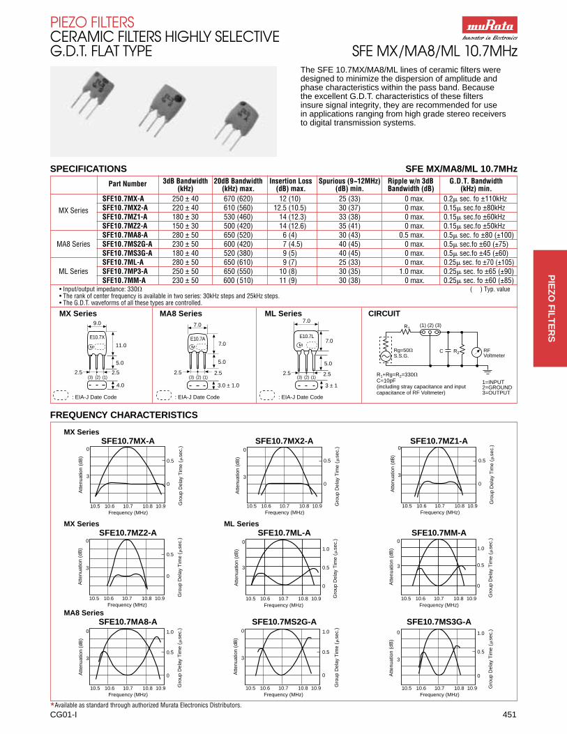
PIEZO FILTERSCERAMIC FILTERS HIGHLY SELECTIVEG.D.T. FLAT TYPE SFE MX/MA8/ML 10.7MHz
The SFE 10.7MX/MA8/ML lines of ceramic filters were designed to minimize the dispersion of amplitude and phase characteristics within the pass band. Because the excellent G.D.T. characteristics of these filters insure signal integrity, they are recommended for use in applications ranging from high grade stereo receivers to digital transmission systems.
�Available as standard through authorized Murata Electronics Distributors.
FREQUENCY CHARACTERISTICS
10.5 10.6 10.7 10.8 10.9Frequency (MHz)
Atte
nuat
ion
(dB
)
0
3
Gro
up D
elay
Tim
e (�
sec.
)
0.5
0
10.5 10.6 10.7 10.8 10.9Frequency (MHz)
Atte
nuat
ion
(dB
)
0
3
Gro
up D
elay
Tim
e (�
sec.
)
0.5
0
10.5 10.6 10.7 10.8 10.9Frequency (MHz)
Atte
nuat
ion
(dB
)
0
3
Gro
up D
elay
Tim
e (�
sec.
)
0.5
0
10.5 10.6 10.7 10.8 10.9Frequency (MHz)
Atte
nuat
ion
(dB
)
0
3
Gro
up D
elay
Tim
e (�
sec.
)
0.5
0
10.5 10.6 10.7 10.8 10.9Frequency (MHz)
Atte
nuat
ion
(dB
)
0
3
Gro
up D
elay
Tim
e (�
sec.
)
1.0
0.5
0
10.5 10.6 10.7 10.8 10.9Frequency (MHz)
Atte
nuat
ion
(dB
)
0
3
Gro
up D
elay
Tim
e (�
sec.
)
1.0
0.5
0
Gro
up D
elay
Tim
e (�
sec.
)
1.0
0.5
0
10.5 10.6 10.7 10.8 10.9Frequency (MHz)
Atte
nuat
ion
(dB
)
0
3
10.5 10.6 10.7 10.8 10.9Frequency (MHz)
Atte
nuat
ion
(dB
)
0
3
Gro
up D
elay
Tim
e (�
sec.
)
1.0
0.5
0 Atte
nuat
ion
(dB
)
0
3
Gro
up D
elay
Tim
e (�
sec.
)
1.0
0.5
0
10.5 10.6 10.7 10.8 10.9Frequency (MHz)
9.0
11.0
2.5 2.5
5.0
7.0
7.0
2.5 2.5
5.0
7.0
7.0
2.5 2.5
5.0
Rg=50�S.S.G.
R1+Rg=R2=330�C=10pF(including stray capacitance and inputcapacitance of RF Voltmeter)
1=INPUT2=GROUND3=OUTPUT
RFVoltmeter
R1
R2C
(1) (2) (3)
E10.7X
M
: EIA-J Date Code : EIA-J Date Code : EIA-J Date Code
E10.7A
M
E10.7L
M
(3) (2) (1) (3) (2) (1) (3) (2) (1)
3 ± 13.0 ± 1.04.0
PIE
ZO
FILT
ER
S

3dB Bandwidth 20dB BandwidthRipple
Insertion Loss Spurious (9 ~ 12MHz)Part Number(kHz) (kHz) max.
Within 3dB(dB) max. (dB) min.Bandwidth (dB)
WideSFE10.7MA19 350 min. (450) 950 (750) 3 max. 3 ± 2 20 (30)
BandwidthSFE10.7MA20-A 330 ± 50 680 (615) 1 max. 4 ± 2 30 (40)
SeriesSFE10.7MA21 400 (500) 950 (750) 3 max. 3 ± 2 20 (30)SFE10.7MHY-A 110 ± 30 350 (260) 1 max. 7 ± 2 30 (42)
• Input/output impedance: 330� (MA20-A, MHY-A), 470� (MA19) ( ) Typ. value• Center frequency 10.52MHz types of SFE10.7MHY-A is also available.
Narrow SFE10.7MTE ±25 (82) 200 (160) 1 max. 5.5 ± 2.5 30 (48)
Bandwidth SFE10.7MVE ±13 (56) 135 (110) 1 max. 5.5 ± 2.0 30 (41)Series SFE10.7MFP ±20 (36) 95 (77) 1 max. 6.0 (2.5) 24 (28)• Input/output impedance: 330 (MT,MV), 600� (MFP) ( ) Typ. value• Spurious range of SFE10.7MFP: 10.7 ± 1MHz.
MA19 Series MTE Series MVE Series MFP Series CIRCUIT
452 CG01-I
PIEZO FILTERSCERAMIC FILTERS LOW LOSS, WIDE ORNARROW BAND, MINIATURE SFE MA/MTE/MVE/MFP 10.7MHz
The following filters were developed to offer both narrower and wider bandwidth characteristics for use in products suchas DBS receivers. These filters also retain the same reliabilitythat is available with our standard filters. The various bandwidths allow these filters to be utilized in a multitude of new communication applications.
Rg=50�S.S.G.
Rg+R1=R2=Input/Output ImpedanceC=10pF(including stray capacitance and inputcapacitance of RF Voltmeter)
1=INPUT2=GROUND3=OUTPUT
RFVoltmeter
R1
R2
C
(1) (2) (3)
SFE10.7MA19 SFE10.7MS2 SFE10.7MS3
FREQUENCY CHARACTERISTICS
10.3 10.5 10.7 10.9 11.1
Frequency (MHz)
Atte
nuat
ion
(dB
)
0
10
20
30
40
Atte
nuat
ion
(dB
)
0
10
20
30
40
�Available as standard through authorized Murata Electronics Distributors.
SPECIFICATIONS SFE MX/MA8/ML 10.7MHz
7.0
7.0
2.5 2.5
5.0
7.0
7.0
5.0
7.0
7.0
5.0A
ttenu
atio
n (d
B)
0
10
20
30
40
10.3 10.5 10.7 10.9 11.1
Frequency (MHz)
10.3 10.5 10.7 10.9 11.1
Frequency (MHz)
2.5 2.5 2.5 2.5
10.0
10.0
5.0
2.5 2.5
E10.7A
ME10.7TM
E10.7VM
3.0 ± 1.0 3.0 ± 1.0 3.0 ± 1.0 3.0 ± 1.0
: EIA-J Date Code : EIA-J Date Code : EIA-J Date Code : EIA-J Date Code
(3) (2) (1) (3) (2) (1) (3) (2) (1)
E10.7F
M
(3) (2) (1)
3dB Bandwidth 40dB BandwidthRipple
Insertion Loss Spurious AttenuationPart Number(kHz) (kHz) max.
within 3dB(dB) max. (9 to 12MHz) (dB) min.Bandwidth (dB)
SFT10.7MA5 280 ± 50 700 (630) 0.5 max. 6 ± 2 50 (60)SFT10.7MS2 230 ± 40 650 (580) 0.5 max. 6 ± 2 50 (60)SFT10.7MS3 180 ± 40 550 (500) 0.5 max. 8 ± 2 50 (60)
• Input/output impedance: 330� ( ) Typ. value• High selectivity is achieved by replacing with SFT10.7 series
DIMENSIONS: mm CIRCUIT
SPECIFICATIONS SFT MA/MS 10.7MHz
CG01-I 453
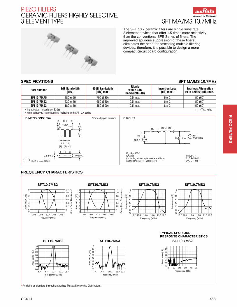
PIEZO FILTERSCERAMIC FILTERS HIGHLY SELECTIVE,3 ELEMENT TYPE SFT MA/MS 10.7MHz
The SFT 10.7 ceramic filters are single substrate, 3 element devices that offer 1.5 times more selectivity than the conventional SFE Series of filters. The improved spurious suppression of these filters eliminates the need for cascading multiple filtering devices; therefore, it is possible to design a more compact circuit board configuration.
Rg+R1=330�C=10pF(including stray capacitance and inputcapacitance of RF Voltmeter.)
1=INPUT2=GROUND3=OUTPUT
RFVoltmeter
R1
Rg
S.S.G.R2 C
(1) (2) (3)
2.5
3.0 ± 0.10.3 ± 0.1
2.5(1) (2) (3)
1 2 3
5.0
6.0
10.0
SFT10.7MS2 SFT10.7MS3 SFT10.7MS3 SFT10.7MS3
TYPICAL SPURIOUSRESPONSE CHARACTERISTICS
SFT10.7MS2 SFT10.7MS3 SFT10.7MS2
FREQUENCY CHARACTERISTICS
10.5 10.6 10.7 10.8 10.9
Frequency (MHz)
Atte
nuat
ion
(dB
)
01
2
3
4
5
67
8.7 9.7 10.7 11.7 12.7
Frequency (MHz)
Atte
nuat
ion
(dB
)
010
20
3040
50607080
8.7 9.7 10.7 11.7 12.7
Frequency (MHz)
Atte
nuat
ion
(dB
)
010
20
3040
50607080
0 10 20 30 40 50
Frequency (kHz)
Atte
nuat
ion
(dB
)
01020
3040506070
Gro
up D
elay
Tim
e (�
sec.
)
1.21.0
0.8
0.6
0.4
0.2
0
10.5 10.6 10.7 10.8 10.9
Frequency (MHz)
Atte
nuat
ion
(dB
)
01
2
3
4
5
67
10.2 10.4 10.6 10.8 11.0 11.2
Frequency (MHz)
Atte
nuat
ion
(dB
)
010
20
30
40
50
6070
10.2 10.4 10.6 10.8 11.0 11.2
Frequency (MHz)
Atte
nuat
ion
(dB
)
010
20
30
40
50
6070G
roup
Del
ay T
ime
(�se
c.)
1.21.0
0.8
0.6
0.40.2
0
�Available as standard through authorized Murata Electronics Distributors.
T10.7*M
: EIA-J Date Code
*Varies by part number
PIE
ZO
FILT
ER
S

Nominal Center 3dB Bandwidth 20dB Bandwidth Insertion LossRipple Spurious Response Withstanding Insulation
Frequency (fn) (kHz) min. (kHz) max. (dB) max.within 3dB (8 ~ 13MHz) Voltage Resistance
Bandwidth (dB) (dB) min. (DC) (M Ohms) min.
10.7MHz ±325 1400 6.0 2.0 max. 23 50V, 1 min. 100 (DC 100V)
• Input/output impedance: 470�
DIMENSIONS: mm TEST CIRCUIT
SPECIFICATIONS KMFC545 10.7MHz
454 CG01-I
PIEZO FILTERSCERAMIC FILTERSULTRA-WIDE BANDWIDTH KMFC545 10.7MHz
New digital applications are pushing the bandwidthrequirements wider on 10.7MHz filters. This matched filterpair is designed to be used in applications that require thewidest possible bandwidth at 10.7MHz. These applicationscan include receivers, audio/video equipment, andmeasurement equipment.
�: INPUT�: GROUND�: OUTPUT: EIA-J Date Code
R1 = 420� ± 5%; R2 = 420� ± 5%; Rg = 50�C2 = 10pF (Including stray capacitance and
Input capacitance of RF Voltmeter)
Insertion Loss (dB) = 20 • logE1(2 • E2
)
M
10.7S
M
10.7P
Series Resonator Parallel Resonator
7.0 ± 2.0
7.0 ± 2.0
6.0 ± 1.0
3.0 ± 1.00.3 ± 0.1
0.5 ± 0.1
1.7 ± 0.11.35 ± 0.2
2.5 ± 0.32.5 ± 0.3
� � �
7.0 ± 2.0
7.0 ± 2.0
6.0 ± 1.0
3.0 ± 1.00.3 ± 0.1
0.5 ± 0.1
1.7 ± 0.11.35 ± 0.2
2.5 ± 0.32.5 ± 0.3
� � �
Blue Dot
� � �
� � �
Series Resonator
ParallelResonator
R1
R2
C2
E2E1
Rg
S.S.G. RFVoltmeter
CG01-I 455
Item Code Dimensions (mm) Note
Adhered Terminal LengthL1 3 min.
L2 2.0 max. Pay attention to directivity
Pitch of Component P 12.7 ± 0.5
Pitch of Sprocket Hole P0 12.7 ± 0.2
Length from Hole Center to Lead P1 3.85 ± 0.5
Length from Hole Center to P2 6.35 ± 0.5Component Center
Lead Spacing (1) F 5.0 +0.5–0.2
Lead Spacing (2) F1 2.5 ± 0.2
Deviation across Tape �h 0 ± 1.0
Deviation along Tape�s 0 ± 1.0
Left or Right
Carrier Tape Width W 18.0 ± 0.5
Hold-down Tape Width W0 6.0 min. Hold-down tape should notoverflow the base tape
Position of Sprocket Hole W1 9.0 ± 0.5
Margin between Both Tapes W2 0 +1.0–0
Lead Distance between H0 18.0 ± 0.5Reference and Bottom Planes
Diameter of Sprocket Hole D0 �4.0 ± 0.2
Total Tape Thickness t 0.6 ± 0.2
SFE10.7M��- * -TF21
TAPING DIMENSIONS
PACKAGING DIMENSIONS: mm
WW
P
P0
t
L1L2 W0
W2
W1
H1
H0
D0
∆S
∆h
P1
P2
F1 F1
F
PIEZO FILTERSCERAMIC FILTERSTAPING & PACKAGING SPECIFICATIONS SFE 10.7MHz
• When packaged, components of different center frequencies are not mixed.• Compatible with various automatic insertion.• Flat pack is the standard package type.
PIE
ZO
FILT
ER
S

Part Nominal Center 3dB Bandwidth Spurious Insertion Loss at Input/OutputNumber Frequency (fn) (MHz)* from fn (kHz) Attenuation min. fn (dB) max. Impedance (Ohms)
SFECV10.7MA21S-TC 10.7 400 min. 20dB (10.7 to 15.0MHz) 3.0 ±2.0 470SFECV10.7MA19S-TC 10.7 350 min. 20dB (10.7 to 15.0MHz) 3.0 ±2.0 470SFECV10.7MA2S-A-TC 10.7 330 ± 50 30dB (9 to 12MHz) 4.0 ±2.0 330SFECV10.7MA5S-A-TC 10.7 280 ± 50 35dB (9 to 12MHz) 3.0 ±2.0 330SFECV10.7MS2S-A-TC 10.7 230 ± 50 35dB (9 to 12MHz) 3.5 ±2.0 330SFECV10.7MS3S-A-TC 10.7 180 ± 40 35dB (9 to 12MHz) 4.0 ±2.0 330SFECV10.7MJS-A-TC 10.7 150 ± 30 35dB (9 to 12MHz) 5.5 ±2.0 330SFECV10.7MHS-A-TC 10.7 110 ± 30 35dB (9 to 12MHz) 6.0 ±2.0 330SFECV10.7 DIMENSIONS: mm TEST CIRCUIT CHARACTERISTICS (Typ.)
SPECIFICATIONS SFECV10.7
* A: 10.70MHz ± 30kHz Z: 10.70MHz ± 90kHz Packaging Units: 2000 pcs/reel (180 mmD)
456 CG01-I
PIEZO FILTERSSURFACE MOUNTED CHIP PIEZOELECTRIC CERAMICS FILTERSFOR AM AND FM APPLICATIONS SFECV 10.7MHz, CFEC 10.8MHz
Along with the development of the AM chip filter, IF filters forAM/FM radios have also been made smaller, thinner and ina chip configuration for surface mounting. This is one moreexample of Murata Electronics’ leadership in convertingconventional electronic components to chip technology.
**
*
(1)(2)(3)
Part Marking1=INPUT * : EIA-J Date Code2=GROUND ** : Center Frequency3=OUTPUT Rank Code
1.0
1.0 1.0
1.0 1.01.0
4.05
1.2
1.2
2.9
1.01.0
6.9
6.9
S.S.G.
RgE1
R1
R2C2
E2
(1)
(2)
(3)
RFVoltmeter
R1+Rg=R2=330ohms ± 1% Rg=50�
C=10pF ± 1pF (Including stray capacitance and input capacitance of RF Voltmeter)
0
10
20
30
4050
6070
9.7 10.2 10.7 11.2 11.7
Frequency (MHz)A
ttenu
atio
n (d
B)
Nominal 3dB 20dB Stopband StopbandSpurious
InsertionGDT
Input/Part Center Bandwidth Bandwidth Attenuation Attenuation
9 to 12MHzLoss at Ripple
DeviationOutput
Number Frequency from fn from fn fn ± 500kHz fn ± 1.2kHz(dB) min.
fn (dB) (dB) max.(�sec) max.
Impedance(fn) (MHz) (kHz) (kHz) max. (dB) min. (dB) min. max. (Ohms)
CFEC10.8MK1-TC 10.8 ±110 to ±150 ±310 37 35 — 6 (fn ± 100kHz) (fn ± 100kHz) 3300.5 1.5
CFEC10.8MG1-TC 10.8 ±135 to ±180 ±350 32 35 — 6 (fn ± 100kHz) (fn ± 100kHz) 3300.5 1.2
CFEC10.8ME11-TC 10.8 ±150 ±420 — — 25 5 (fn ± 110kHz) (fn ± 110kHz) 3301 1.5
CFEC10.8MD11-TC 10.8 ±170 ±450 — — 25 5 (fn ± 170kHz) (fn ± 170kHz) 6001 2.0
CFEC10.8 DIMENSIONS: mm PLASTIC TAPE (for SFECV & CFEC) PLASTIC REEL
SPECIFICATIONS CFEC10.8*
***
1.0 ± 0.5 1.0 ± 0.3 1.0 ± 0.5
6.9 ± 0.3 1.5 ± 0.2
2.9
± 0.
3
1.0 ± 0.5 1.2 ± 0.5 1.0 ± 0.5
1.0 ± 0.5
6.9 ± 0.33.95 ± 0.4
1.0 ± 0.3
1.0 ± 0.5
(1) (2) (3)
D
4.0 ± 0.1
4.0 ± 0.12.0 ± 0.05
+0.1–0�1.5
5.5
± 0.
05
+0.
08–0
.212
.0
+0.
1–0
.05
1.7
7.3
± 0.
1
0.3
± 0.
05
0.05
1.9
± 0.
1
Direction of Feed
Chip Filter3.3 ± 0.1
3° max.10° max.Cover
Film
CavityTape
(�18
0)
�13.0 ± 0.5
20.5 max.
14.0 ± 1.5
2.0 ± 0.5
* : EIA-J Date Code** : Center Frequency
Rank Code
1=INPUT (or Output)2=GROUND3=OUTPUT (or Input)
Note: Marked sides face to cover tape. Lead positions are as per abovefigure. One kind of frequency rank filters are packed in a reel.
Note: No parts in leader cavity and tail end.2000 pcs min./reel
Peel back force20 ~ 60gr
* CFEC also available with center frequency of 10.75 or 10.7 MHz.
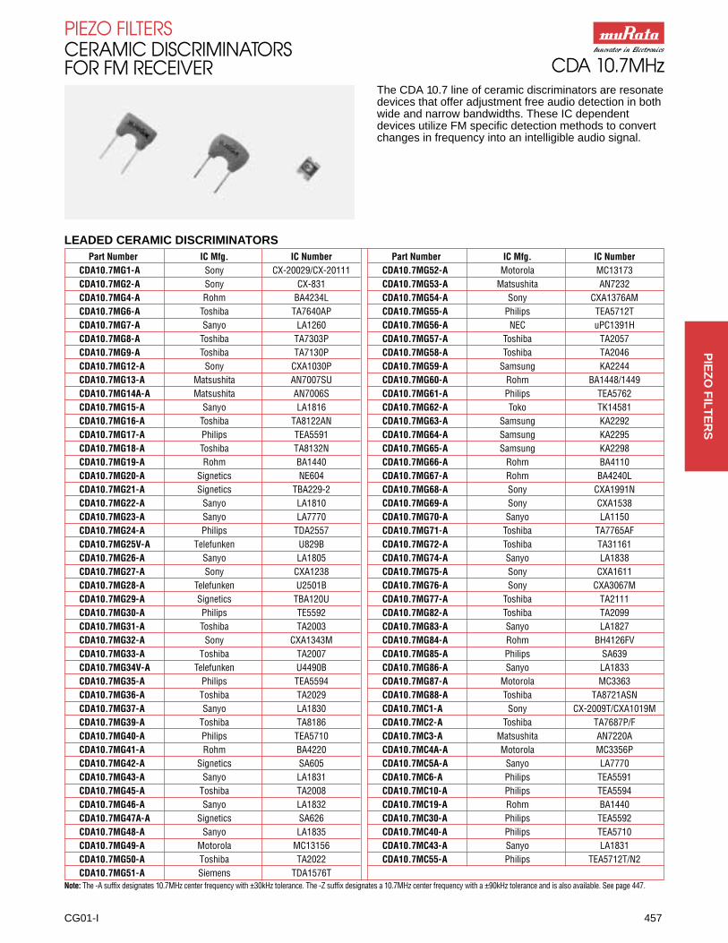
Part Number IC Mfg. IC NumberCDA10.7MG1-A Sony CX-20029/CX-20111CDA10.7MG2-A Sony CX-831CDA10.7MG4-A Rohm BA4234LCDA10.7MG6-A Toshiba TA7640APCDA10.7MG7-A Sanyo LA1260CDA10.7MG8-A Toshiba TA7303PCDA10.7MG9-A Toshiba TA7130PCDA10.7MG12-A Sony CXA1030PCDA10.7MG13-A Matsushita AN7007SUCDA10.7MG14A-A Matsushita AN7006SCDA10.7MG15-A Sanyo LA1816CDA10.7MG16-A Toshiba TA8122ANCDA10.7MG17-A Philips TEA5591CDA10.7MG18-A Toshiba TA8132NCDA10.7MG19-A Rohm BA1440CDA10.7MG20-A Signetics NE604CDA10.7MG21-A Signetics TBA229-2CDA10.7MG22-A Sanyo LA1810CDA10.7MG23-A Sanyo LA7770CDA10.7MG24-A Philips TDA2557CDA10.7MG25V-A Telefunken U829BCDA10.7MG26-A Sanyo LA1805CDA10.7MG27-A Sony CXA1238CDA10.7MG28-A Telefunken U2501BCDA10.7MG29-A Signetics TBA120UCDA10.7MG30-A Philips TE5592CDA10.7MG31-A Toshiba TA2003CDA10.7MG32-A Sony CXA1343MCDA10.7MG33-A Toshiba TA2007CDA10.7MG34V-A Telefunken U4490BCDA10.7MG35-A Philips TEA5594CDA10.7MG36-A Toshiba TA2029CDA10.7MG37-A Sanyo LA1830CDA10.7MG39-A Toshiba TA8186CDA10.7MG40-A Philips TEA5710CDA10.7MG41-A Rohm BA4220CDA10.7MG42-A Signetics SA605CDA10.7MG43-A Sanyo LA1831CDA10.7MG45-A Toshiba TA2008CDA10.7MG46-A Sanyo LA1832CDA10.7MG47A-A Signetics SA626CDA10.7MG48-A Sanyo LA1835CDA10.7MG49-A Motorola MC13156CDA10.7MG50-A Toshiba TA2022CDA10.7MG51-A Siemens TDA1576T
Part Number IC Mfg. IC NumberCDA10.7MG52-A Motorola MC13173CDA10.7MG53-A Matsushita AN7232CDA10.7MG54-A Sony CXA1376AMCDA10.7MG55-A Philips TEA5712TCDA10.7MG56-A NEC uPC1391HCDA10.7MG57-A Toshiba TA2057CDA10.7MG58-A Toshiba TA2046CDA10.7MG59-A Samsung KA2244CDA10.7MG60-A Rohm BA1448/1449CDA10.7MG61-A Philips TEA5762CDA10.7MG62-A Toko TK14581CDA10.7MG63-A Samsung KA2292CDA10.7MG64-A Samsung KA2295CDA10.7MG65-A Samsung KA2298CDA10.7MG66-A Rohm BA4110CDA10.7MG67-A Rohm BA4240LCDA10.7MG68-A Sony CXA1991NCDA10.7MG69-A Sony CXA1538CDA10.7MG70-A Sanyo LA1150CDA10.7MG71-A Toshiba TA7765AFCDA10.7MG72-A Toshiba TA31161CDA10.7MG74-A Sanyo LA1838CDA10.7MG75-A Sony CXA1611CDA10.7MG76-A Sony CXA3067MCDA10.7MG77-A Toshiba TA2111CDA10.7MG82-A Toshiba TA2099CDA10.7MG83-A Sanyo LA1827CDA10.7MG84-A Rohm BH4126FVCDA10.7MG85-A Philips SA639CDA10.7MG86-A Sanyo LA1833CDA10.7MG87-A Motorola MC3363CDA10.7MG88-A Toshiba TA8721ASNCDA10.7MC1-A Sony CX-2009T/CXA1019MCDA10.7MC2-A Toshiba TA7687P/FCDA10.7MC3-A Matsushita AN7220ACDA10.7MC4A-A Motorola MC3356PCDA10.7MC5A-A Sanyo LA7770CDA10.7MC6-A Philips TEA5591CDA10.7MC10-A Philips TEA5594CDA10.7MC19-A Rohm BA1440CDA10.7MC30-A Philips TEA5592CDA10.7MC40-A Philips TEA5710 CDA10.7MC43-A Sanyo LA1831CDA10.7MC55-A Philips TEA5712T/N2
CG01-I 457
PIEZO FILTERSCERAMIC DISCRIMINATORSFOR FM RECEIVER CDA 10.7MHz
The CDA 10.7 line of ceramic discriminators are resonatedevices that offer adjustment free audio detection in bothwide and narrow bandwidths. These IC dependentdevices utilize FM specific detection methods to convertchanges in frequency into an intelligible audio signal.
Note: The -A suffix designates 10.7MHz center frequency with ±30kHz tolerance. The -Z suffix designates a 10.7MHz center frequency with a ±90kHz tolerance and is also available. See page 447.
LEADED CERAMIC DISCRIMINATORS
PIE
ZO
FILT
ER
S

458 CG01-I
PIEZO FILTERSCERAMIC DISCRIMINATORSFOR FM DEMODULATION RECEIVERS CDACV 10.7MHz
LEADED DIMENSIONS: mm TYPICAL CIRCUITCDA TYPE
SURFACE MOUNT DIMENSIONS: mm RECOMMENDABLE LAND PATTERN: mmCDACV TYPE
Part Number IC Mfg. IC Number
CDACV10.7MC1-A-TC Sony CX-20091
CDACV10.7MG1-A-TC Sony CX-20029
CDACV10.7MG16F-A-TC Toshiba TA8122AF
CDACV10.7MG18-A-TC Toshiba TA8132F
CDACV10.7MC40-A-TC Philips TEA5710
CDACV10.7MG50-A-TC Toshiba TA2022
CDACV10.7MG51-A-TC Siemens TDA1576T
CDACV10.7MG53-A-TC National AN7232
CDACV10.7MG54-A-TC Sony CXA1376
CDACV10.7MG69-A-TC Sony CXA1538N
SURFACE MOUNT CERAMIC DISCRIMINATORS
� � � � � � �
� � � � � �
8.0 ± 1.0
10.7G ** 5.0 ± 1.0
3.4 ± 0.5
2.6 ± 0.3
1.5 ± 0.3 1.5
FM SSGCDA 10.7MG20
DC OUT
AF Output
0.01�
0.01�
0.1� 10p
100p
100p
Vcc(+6.0V)
0.1�
47�
0.1�
1.5k
0.9 ± 0.30.9 ± 0.3
Color Code
** : EIA-J Date Code
5.0 ± 1.00.65 ± 0.1
0.5 ± 0.1
0.3 ± 0.1
3.0 ± 1.0
5.0 ± 0.2
M
1.5
2.6
1.4 1.5 1.4
* : EIA-J Date Code** : Center Frequency Rank Code
**
*
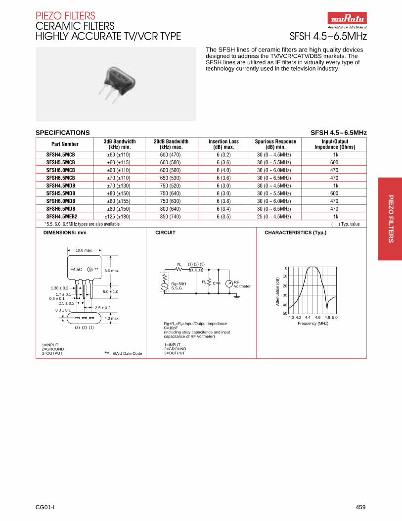
CG01-I 459
PIEZO FILTERSCERAMIC FILTERSHIGHLY ACCURATE TV/VCR TYPE SFSH 4.5–6.5MHz
The SFSH lines of ceramic filters are high quality devicesdesigned to address the TV/VCR/CATV/DBS markets. TheSFSH lines are utilized as IF filters in virtually every type oftechnology currently used in the television industry.
Part Number 3dB Bandwidth 20dB Bandwidth Insertion Loss Spurious Response Input/Output(kHz) min. (kHz) max. (dB) max. (dB) min. Impedance (Ohms)
SFSH4.5MCB ±60 (±110) 600 (470) 6 (3.2) 30 (0 ~ 4.5MHz) 1kSFSH5.5MCB ±60 (±115) 600 (500) 6 (3.6) 30 (0 ~ 5.5MHz) 600SFSH6.0MCB ±60 (±110) 600 (500) 6 (4.0) 30 (0 ~ 6.0MHz) 470SFSH6.5MCB ±70 (±110) 650 (530) 6 (3.6) 30 (0 ~ 6.5MHz) 470SFSH4.5MDB ±70 (±130) 750 (520) 6 (3.0) 30 (0 ~ 4.5MHz) 1kSFSH5.5MDB ±80 (±150) 750 (640) 6 (3.0) 30 (0 ~ 5.5MHz) 600SFSH6.0MDB ±80 (±155) 750 (630) 6 (3.8) 30 (0 ~ 6.0MHz) 470SFSH6.5MDB ±80 (±150) 800 (640) 6 (3.4) 30 (0 ~ 6.5MHz) 470SFSH4.5MEB2 ±125 (±180) 850 (740) 6 (3.5) 25 (0 ~ 4.5MHz) 1k
*5.5, 6.0, 6.5MHz types are also available ( ) Typ. value
DIMENSIONS: mm CIRCUIT CHARACTERISTICS (Typ.)
SPECIFICATIONS SFSH 4.5–6.5MHz
10.0 max.
8.0 max.F4.5C **
5.0 ± 1.0
4.0 max.
2.5 ± 0.22.5 ± 0.2
0.3 ± 0.1
0.5 ± 0.11.7 ± 0.1
1.38 ± 0.2Rg=50�S.S.G.
Rg+R1=R2=Input/Output ImpedanceC=10pF(including stray capacitance and inputcapacitance of RF Voltmeter)
1=INPUT2=GROUND3=OUTPUT
1=INPUT2=GROUND3=OUTPUT ** : EIA-J Date Code
RFVoltmeter
R1
R2 C
(1) (2) (3)
(3) (2) (1)
4.0 4.2 4.4 4.6 4.8 5.0
Frequency (MHz)
Atte
nuat
ion
(dB
)
0
10
20
30
40
50
M
PIE
ZO
FILT
ER
S

Part Number Nominal Center Attenuation 20dB Attenuation Spurious ResponseFrequency (fn) at fn (dB) min. Bandwidth (kHz) min. (0 to fn) (dB) max.
�TPS3.58MJ 3.58MHz 20 (27) 20 (30) 0.5 (0)TPS4.43MJ 4.43MHz 20 (30) 40 (50) 0.5 (0)
�TPS4.5MJ 4.5MHz 20 (30) 30 (50) 0.5 (0)�TPS5.5MJ 5.5MHz 20 (30) 30 (60) 0.5 (0)�TPS6.0MJ 6.0MHz 20 (30) 40 (70) 0.5 (0)
TPS6.5MJ 6.5MHz 20 (30) 40 (90) 0.5 (0)( ) Typ. value
DIMENSIONS: mm CIRCUIT CHARACTERISTICS
SPECIFICATIONS TPS MJ 4.5–6.5MHz
Part NumberNominal Center Attenuation 30dB Attenuation Spurious ResponseFrequency (fn) at fn (dB) min. Bandwidth (kHz) min. (0 to fn) (dB) max.
�TPS4.5MB2 4.5MHz 35 (45) 50 (80) 0.5 (0)�TPS5.5MB 5.5MHz 35 (45) 70 (120) 0.5 (0)�TPS6.0MB 6.0MHz 35 (45) 70 (120) 0.5 (0)�TPS6.5MB 6.5MHz 35 (45) 70 (120) 0.5 (0)
The level at 1 MHz shall be made for a reference (0dB) ( ) Typ. valueOther frequencies (3.58, 4.43 MHz) are also available.
DIMENSIONS: mm CIRCUIT CHARACTERISTICS
TPS4.5 (4.5 ± 0.5MHz)
SPECIFICATIONS TPS MB 4.5–6.5 MHz
460 CG01-I
PIEZO FILTERSCERAMIC TRAPSHIGH ATTENUATION TPS MJ/MB 4.5–6.5MHz
The TPS MJ/MB lines of ceramic traps are band reject filtersused for video and sound IF attenuation. The 2 terminal TPS MJ Series can be used to attenuate either the sound signal in B/W receivers or the chroma signal in video. The 3 terminal TPS MB Series contains 2 trap elements on one substrate for additional attenuation. This line of traps can beused in the sound IF of CATV/VCR receivers.
3.5 4.0 4.5 5.0 5.5
Frequency (MHz)
Atte
nuat
ion
(dB
)
0
10
20
30
40
50
6070
S.S.G.Rg=50�
10.0
10.0
5.0
5.0
RFVoltmeter
75�
50�1k�
4.00 4.25 4.50 4.75 5.00
Frequency (MHz)
Atte
nuat
ion
(dB
)
0
10
20
30
40
50
6070
Rg=50
S.S.G.
7.0
T4.5B
T4.5J
7.0
5.0
2.52.5
RFVoltmeter
75� L
50� R
�Available as standard through authorized Murata Electronics Distributors.
5.0 max.
3.0 ± 0.2
L RMB2 8.2�H 2.2k�
Other 15�H 1.0k�

CG01-I 461
PIEZO FILTERSCERAMIC DISCRIMINATORSFOR QUADRATURE DETECTION CDA MC/ME 4.5–6.5MHz
The CDA MC/ME lines of ceramic discriminators are ICdependent devices used in the recovery of audio signals.The CDA MC discriminators have three terminals whilethe CDA ME discriminators are 2 terminal devices.
Part Number IC Part Number IC Part Number ICCDA�MC10 TBA120T CDA�MC22 M51354AP CDA�MC30 M51348FPCDA�MC15 TA7146P CDA�MC23 M51316P CDA�MC31 TDA4282TCDA�MC16 TDA4940 CDA�MC24B LA7520 CDA�MC32 LA7522CDA�MC17 TDA4280 CDA�MC25 LA7521 CDA�MC33 �PC1416GCDA�MC18 HA11229 CDA�MC26 LA7530 (N) CDA�MC34 TBA130-2CDA�MC19 �PC1391H CDA�MC27 �PC1411CA CDA�MC35 M51345FPCDA�MC20 �PC1382C CDA�MC28 M51316BPCDA�MC21 �PC1383C CDA�MC29 M51365SP
� Indicates frequency 4.5, 5.5, 5.74, 6.0, 6.5 MHz are available. Note that part numbers, circuits and ratings vary according to the IC used at detector process.
DIMENSIONS: mm CIRCUIT RECOVERED AUDIO CHARACTERISTICS
CDA 4.5 MC20 CDA 4.5 MC20
MATCHING IC CDA MC 4.5–6.5MHz
(1)=INPUT(2)=GROUND(3)=OUTPUT
4.4 4.5 4.6Frequency (MHz)
Test Conditions= 100 dBV400 H2, ± 7.5kH2 Dev.
AF Output300
100
10
1
AF
Out
put
(mV
)
7.5
9.0
5.00.6
2.5
4.0 max.
2.5
Part Number IC Part Number IC Part Number ICCDA�ME1 CX-20014 CDA�ME8 TBA129 CDA�ME23 M51496PCDA�ME2 AN5135 CDA�ME10 TDA2546A CDA�ME27 LA7650CDA�ME3 TA7678AP CDA�ME19 M51346BP CDA�ME30 CXA1110ASCDA�ME5 AN5135NK CDA�ME20 LA7550 CDA�ME34 TA8680NCDA�ME6 M51346AP CDA�ME21 LA7545 CDA�ME35 LA7680CDA�ME7 TDA4503 CDA�ME22 TDA2556 CDA�ME37 TA8691N
� Indicates frequency 4.5, 5.5, 5.74, 6.0, 6.5 MHz are available. Note that part numbers, circuits and ratings vary according to the IC used at detector process.
DIMENSIONS: mm CIRCUIT
CDA 4.5 ME20
MATCHING IC CDA ME 4.5–6.5MHz
14 6 11 9 10 3
13 7 8 4 12 1
S.S.G.
(FM-AMRg=50)
50
.01�
10�/16V
47�25V
.01�
.01�
.01�
47�/25V
.01�DC Supply
10�16V47k
220
12.0V
AF Output
DC Output
(1)
(2)
(3)470
47k 10k
IC:�PC1382C(NEC)
Distortion Dis
tort
ion
(%)
10
1.0
0.1
10.0
10.0
5.00.6
5.0 max.
5.0
VoltmeterRecovered
Audio Signal
Ground
0.01�
0.01�
FM S.S.G.Signal Input
+5.0VDC
Voltage Supply+12.0VDC0.01�
0.01�0.01�0.01�
100�22�
0.01�
5.6k
0.015�
CDA4.5ME20
24 LA7550
20 19 18 17 15 14 1 3
1 2 6 7 8 9 11 12
0.01
�82
0
: EIA-J Date Code
: EIA-J Date Code
CDA4.5MCM
D4.5Z
M
PIE
ZO
FILT
ER
S

462 CG01-I
PIEZO FILTERSSAW FILTERS FOR AUDIO VISUAL EQUIPMENTCOLOR TV/VCR SIF SAF Series
This series of saw filters is designed for TV/VCR applications. These filters are capable of passing 1) SIF and PIF, 2) SIF or 3) PIF. Saw filters are made up of zincoxide on a glass substrate. Murata provides saw filters for avariety of television standards worldwide.
SPECIFICATIONS SAF MHz
Insertion Picture ChromaAttenuation Attenuation Adjacent Adjacent Spurious Spurious Temperature
Part Number Loss Carrier Carrier(dB) max. (dB) max. Sound Picture Response Response Coefficient
(dB) max. (dB) max. (dB) min.at fs– at fs+ Carrier Carrier (dB) min. (dB) min. (ppm/°C)0.3MHz 0.3MHz (dB) min. (dB) min.
SAF54MC200Z 16(13) 40 min. 17 3 3 40 3728 30
–28 ± 20(0~52.75MHz) (56.75~70MHz)
SAF41MC200Z 17(14) 40 min. 17 3 3 40 3728 30
–28 ± 20(0~39.75MHz) (43.75~56MHz)
SAF39.2MC70Z 19(14) 40 min. 35 6 6 40 3030 30
–10 ± 20(28~31.2MHz) (40.7~45MHz)
SAF33.4MC200Z 20(18) 40 min. 20 4 4 40 3530 30
–10 ± 20(0~31.9MHz) (40.4~47MHz)
SAF54MD200Z 20(17)within
20fs~0.2MHz fs~0.2MHz
35 3030 151
–28 ± 20±3 3 3 (0~70MHz) (55.5~57.5MHz)
SAF41MD200Z 17(14)within
20fs~0.2MHz fs~0.2MHz
35 3530 151
–28 ± 20±3 3 3 (0~55MHz) (42.5~44.5MHz)
SAF33.4MD200Z 20.5(16)within
20fs~0.2MHz fs~0.2MHz
35 3530 151
–10 ± 20±3 3 3 (0~50MHz) (34.67~37.7MHz)
SAF33.0MDA70Z 26(23) 5.0 ± 3.0 12fs~0.2MHz fs~0.2MHz
26 2015 81
–10 ± 203 3 (0~39.5MHz) (34.67~37.7MHz)
SAF32.9MDE70Z 25(23) 4.3 ± 3.0 15fs~0.2MHz fs~0.2MHz
35 2522 101
–10 ± 203 3 (0~31.5MHz) (35.27~38MHz)
within fs~0.2MHz fs~0.2MHz 301 151
SAF31.4MD70Z 28(26)±3
153 3
35 35(0~45MHz)
(32.645~ –10 ± 2035.675MHz)
DIMENSIONS: mm SAF–200Z DIMENSIONS: mm SAF–70Z
SAF54MC200Z SAF41MC200Z SAF33.4MD200Z
FREQUENCY CHARACTERISTICS
10dB/div.
2dB/div.
52 54 56 58 60 62
Frequency (MHz)
Atte
nuat
ion
(dB
)
0
10
20
30
40
50
60
70
5
4
3
2
1
0
Gro
up D
elay
Tim
e (�
sec.
)
10dB/div.
2dB/div.
39 41 43 45 47 49
Frequency (MHz)
Atte
nuat
ion
(dB
)
0
10
20
30
40
50
60
70
5
4
3
2
1
0
Gro
up D
elay
Tim
e (�
sec.
)
10dB/div.
2dB/div.
31 33 35 37 39 41
Frequency (MHz)
Atte
nuat
ion
(dB
)
0
10
20
30
40
50
60
70
5
4
3
2
1
0
Gro
up D
elay
Tim
e (�
sec.
)
* : EIA-J Date Code
15.0 max.
41C 9.0 max.
4.0 min.
6.0 max.
0.5 ± 0.1
0.3 ± 0.1
� � � � �
2.52.52.52.5
*
� Input� Input Ground� Ground� Output� Output
Input Mark
M
* : EIA-J Date Code
14.0 max.
32.9DE 10.0 max.
4.0 min.
5.0 max.
0.6 ± 0.1
0.3 ± 0.1
� � � � �
2.52.52.52.5
*
� Input� Input Ground� Ground� Output� Output
Input Mark
• SAF54MC200Z, SAF41MC200Z and SAF33.4MC2OOZ are for Split Carrier System.• SAF54MD200Z, SAF41MD200Z, SAF33.4MD200Z and SAF31.4MD70Z are for
Quasi-Parallel System.
• SAF33.0MDA70Z is for Multi-Sound TV in Northern Europe.• SAF32.9MDE70Z is for Multi-Sound TV in U.K.• 0dB level should be at fs.
( ): Typ. values1Minimum attenuation betweenpicture carrier and sound carrier
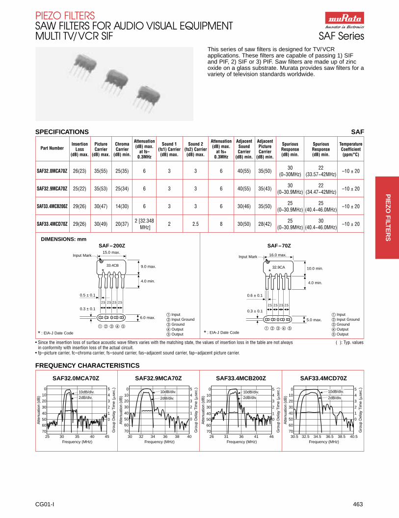
CG01-I 463
PIEZO FILTERSSAW FILTERS FOR AUDIO VISUAL EQUIPMENTMULTI TV/VCR SIF SAF Series
This series of saw filters is designed for TV/VCR applications. These filters are capable of passing 1) SIF and PIF, 2) SIF or 3) PIF. Saw filters are made up of zincoxide on a glass substrate. Murata provides saw filters for avariety of television standards worldwide.
SPECIFICATIONS SAF
Insertion Picture ChromaAttenuation
Sound 1 Sound 2Attenuation Adjacent Adjacent
Spurious Spurious TemperaturePart Number Loss Carrier Carrier
(dB) max.(fs1) Carrier (fs2) Carrier
(dB) max. Sound PictureResponse Response Coefficient
(dB) max. (dB) max. (dB) min.at fs–
(dB) max. (dB) max.at fs+ Carrier Carrier
(dB) min. (dB) min. (ppm/°C)0.3MHz 0.3MHz (dB) min. (dB) min.
SAF32.0MCA70Z 26(23) 35(55) 25(35) 6 3 3 6 40(55) 35(50) 30 22(0~30MHz) (33.57~42MHz)
–10 ± 20
SAF32.9MCA70Z 25(22) 35(53) 25(34) 6 3 3 6 40(55) 35(43) 30 22(0~30.9MHz) (34.47~42MHz)
–10 ± 20
SAF33.4MCB200Z 29(26) 30(47) 14(30) 6 3 3 6 30(46) 35(50) 25 25(0~30.9MHz) (40.4~46.0MHz)
–10 ± 20
SAF33.4MCD70Z 29(26) 30(49) 20(37) 2 [32.348 2 2.5 8 30(50) 28(42) 25 30MHz] (0~30.9MHz) (40.4~46.0MHz)
–10 ± 20
DIMENSIONS: mmSAF–200Z SAF–70Z
16.0 max.
32.9CA 10.0 min.
4.0 min.
5.0 max.
0.6 ± 0.1
0.3 ± 0.1
2.5 2.5 2.5 2.5
*
15.0 max.
33.4CB 9.0 max.
4.0 min.
6.0 max.
0.5 ± 0.1
0.3 ± 0.1
� � � � � � � � � �
2.52.52.52.5
*
� Input� Input Ground� Ground� Output� Output
� Input� Input Ground� Ground� Output� Output
Input Mark Input Mark
SAF32.0MCA70Z SAF32.9MCA70Z SAF33.4MCB200Z SAF33.4MCD70Z
FREQUENCY CHARACTERISTICS
5
4
3
2
1
0
0
10
20
30
40
50
60
7025 30 35 40 45
Frequency (MHz)
Atte
nuat
ion
(dB
)
Gro
up D
elay
Tim
e (�
sec.
)
10dB/div.2dB/div.
5
4
3
2
1
0
0
10
20
30
40
50
60
7030 34 36 38 40
Frequency (MHz)
Atte
nuat
ion
(dB
)
Gro
up D
elay
Tim
e (�
sec.
)
10dB/div.
2dB/div.
32
5
4
3
2
1
0
0
10
20
30
40
50
60
7026 31 36 41 46
Frequency (MHz)
Atte
nuat
ion
(dB
)
Gro
up D
elay
Tim
e (�
sec.
)
10dB/div.2dB/div.
5
4
3
2
1
0
0
10
20
30
40
50
60
7030.5 34.5 36.5 38.5 40.5
Frequency (MHz)
Atte
nuat
ion
(dB
)
Gro
up D
elay
Tim
e (�
sec.
)
32.5
10dB/div.
2dB/div.
• Since the insertion loss of surface acoustic wave filters varies with the matching state, the values of insertion loss in the table are not always ( ): Typ. valuesin conformity with insertion loss of the actual circuit.
• fp–picture carrier, fc–chroma carrier, fs–sound carrier, fas–adjacent sound carrier, fap–adjacent picture carrier.
* : EIA-J Date Code * : EIA-J Date Code
PIE
ZO
FILT
ER
S
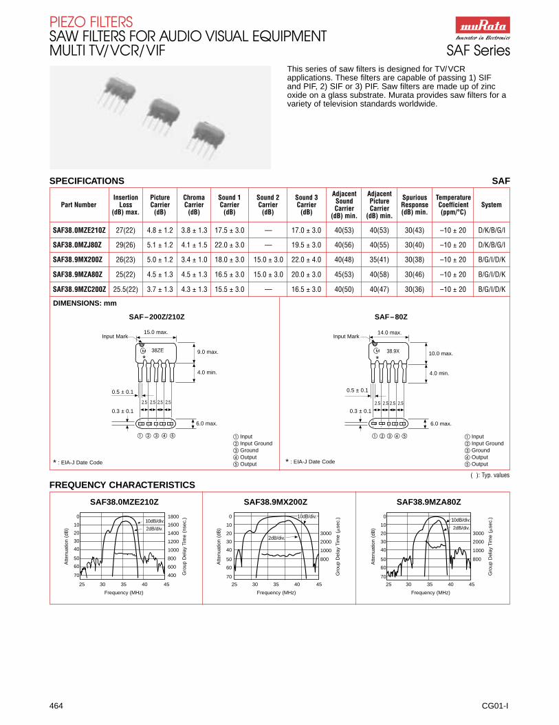
464 CG01-I
PIEZO FILTERSSAW FILTERS FOR AUDIO VISUAL EQUIPMENTMULTI TV/VCR/VIF SAF Series
This series of saw filters is designed for TV/VCR applications. These filters are capable of passing 1) SIF and PIF, 2) SIF or 3) PIF. Saw filters are made up of zincoxide on a glass substrate. Murata provides saw filters for avariety of television standards worldwide.
SPECIFICATIONS SAF
Insertion Picture Chroma Sound 1 Sound 2 Sound 3 Adjacent Adjacent Spurious TemperaturePart Number Loss Carrier Carrier Carrier Carrier Carrier Sound Picture Response Coefficient System
(dB) max. (dB) (dB) (dB) (dB) (dB) Carrier Carrier (dB) min. (ppm/°C)(dB) min. (dB) min.
SAF38.0MZE210Z 27(22) 4.8 ± 1.2 3.8 ± 1.3 17.5 ± 3.0 — 17.0 ± 3.0 40(53) 40(53) 30(43) –10 ± 20 D/K/B/G/I
SAF38.0MZJ80Z 29(26) 5.1 ± 1.2 4.1 ± 1.5 22.0 ± 3.0 — 19.5 ± 3.0 40(56) 40(55) 30(40) –10 ± 20 D/K/B/G/I
SAF38.9MX200Z 26(23) 5.0 ± 1.2 3.4 ± 1.0 18.0 ± 3.0 15.0 ± 3.0 22.0 ± 4.0 40(48) 35(41) 30(38) –10 ± 20 B/G/I/D/K
SAF38.9MZA80Z 25(22) 4.5 ± 1.3 4.5 ± 1.3 16.5 ± 3.0 15.0 ± 3.0 20.0 ± 3.0 45(53) 40(58) 30(46) –10 ± 20 B/G/I/D/K
SAF38.9MZC200Z 25.5(22) 3.7 ± 1.3 4.3 ± 1.3 15.5 ± 3.0 — 16.5 ± 3.0 40(50) 40(47) 30(36) –10 ± 20 B/G/I/D/K
DIMENSIONS: mm
SAF–200Z/210Z SAF–80Z
SAF38.0MZE210Z SAF38.9MX200Z SAF38.9MZA80Z
FREQUENCY CHARACTERISTICS
25 30 35 40 45
Frequency (MHz)
Atte
nuat
ion
(dB
)
0
10
20
30
40
50
60
70
10dB/div.
2dB/div.
Gro
up D
elay
Tim
e (n
sec.
)1800
1600
1400
1200
1000
800
600
400
10dB/div.
25 30 35 40 45
Frequency (MHz)
Atte
nuat
ion
(dB
)
0
10
20
30
40
50
60
70
2dB/div.
Gro
up D
elay
Tim
e (�
sec.
)
3000
2000
1000
800
25 30 35 40 45
Frequency (MHz)
Atte
nuat
ion
(dB
)
0
10
20
30
40
50
60
70
10dB/div.
2dB/div.
Gro
up D
elay
Tim
e (�
sec.
)
3000
2000
1000
800
( ): Typ. values
15.0 max.
38ZE 9.0 max.
4.0 min.
6.0 max.
0.5 ± 0.1
0.3 ± 0.1
� � � � �
2.52.52.52.5
*
� Input� Input Ground� Ground� Output� Output
� Input� Input Ground� Ground� Output� Output
Input Mark Input Mark14.0 max.
38.9X 10.0 max.
4.0 min.
6.0 max.
0.5 ± 0.1
0.3 ± 0.1
� � � � �
2.5 2.5 2.5 2.5
*M M
* : EIA-J Date Code * : EIA-J Date Code

CG01-I 465
PIEZO FILTERSSAW FILTERSFOR AUDIO VISUAL EQUIPMENT SAF Series
This series of saw filters is designed for TV/VCR applications. These filters are capable of passing 1) SIF and PIF, 2) SIF or 3) PIF. Saw filters are made up of zincoxide on a glass substrate. Murata provides saw filters for a variety of television standards worldwide.
SPECIFICATIONS SAFInsertion Picture Chroma Sound Adjacent Attenuation at Attenuation at Adjacent Attenuation at Spurious Temperature
Part Number Loss Carrier Carrier Carrier Sound Carrier fas +1.0MHz fap –0.5MHz Picture Carrier fap –0.5 MHz Response Coefficient(dB) max. (dB) (dB) (dB) (dB) min. (dB) min. (dB) min. (dB) min. (dB) min. (dB) min. (ppm/°C)
SAF38.9MZ215Z 24.0(19) 5.0 ± 1.2 5.8 ± 1.5 19.0 ± 2 44(56) 42(52) — 45(50) — 36 –10 ± 20SAF38.9MZR80Z 24.0(22) 4.5 ± 1.2 4.5 ± 1.5 22.0 ± 3 40(48) 38(48) 35(45) 40(48) 37(50) 30 –10 ± 20SAF38.9MZW210Z 22.5(20) 4.5 ± 1.2 3.1 ± 1.0 17.5 ± 3 43(54) 38(52) 38(42) 36(42) 38(42) 33 –10 ± 20DIMENSIONS: mm SAF–210Z/215Z DIMENSIONS: mm SAF–80Z
SAF38.9MZ215Z SAF38.9MZR80Z SAF38.9MZW210Z
FREQUENCY CHARACTERISTICS
10dB/div.
2dB/div.
25 29 33 37 41 45
Frequency (MHz)
Atte
nuat
ion
(dB
)
0
10
20
30
40
50
60
70
1800
1600
1400
1200
1000
800
600
400 Gro
up D
elay
Tim
e (n
sec.
)
10dB/div.
2dB/div.
26 30 34 38 42 46
Frequency (MHz)
Atte
nuat
ion
(dB
)
0
10
20
30
40
50
60
70
1800
1600
1400
1200
1000
800
600
400 Gro
up D
elay
Tim
e (n
sec.
) 10dB/div.
2dB/div.
31 33 35 37 39 41
Frequency (MHz)
Atte
nuat
ion
(dB
)
0
10
20
30
40
50
60
70
1800
1600
1400
1200
1000
800
600
400 Gro
up D
elay
Tim
e (n
sec.
)
SPECIFICATIONS SAFInsertion Picture Chroma Sound Attenuation at Adjacent Adjacent Spurious Temperature
Part Number Loss Carrier Carrier Carrier at fp –4.0MHz Sound Carrier Picture Carrier Response Coefficient(dB) max. (dB) (dB) (dB) (dB) max. (dB) min. (dB) min. (dB) min. (ppm/°C)
SAF58MVG80Z 23(20) 4.8 ± 1.2 1.0 20 5.0(2.0) 40(53) 40(58) 30 –28 ± 20SAF45MVE80Z 23(20) 5.0 ± 1.2 1.2 20 5.5(2.7) 40(48) 40(53) 28 –28 ± 20DIMENSIONS: mm FREQUENCY CHARACTERISTICS
SAF58MVG80Z SAF45MVE80Z
* : EIA-J Date Code
15.0 max.
38.9ZW 9.0 max.
4.0 min.
6.0 max.
0.5 ± 0.1
0.3 ± 0.1
� � � � �
2.52.52.52.5
*
� Input� Input Ground� Ground� Output� Output * : EIA-J Date Code
14.0 max.
58VG 10.0 max.
4.0 min.
6.0 max.
0.5 ± 0.1
0.3 ± 0.1
� � � � �
2.52.52.52.5
*
� Input� Input Ground� Ground� Output� Output
Input MarkInput Mark
M
* : EIA-J Date Code
16.0 max.
58VG 10.0 max.
4.0 min.
6.0 max.
0.5 ± 0.1
0.3 ± 0.1
� � � � �
2.52.52.52.5
*
� Input� Input Ground� Ground� Output� Output
Input Mark
M
M
10dB/div.
2dB/div.
52 54 56 58 60 62
Frequency (MHz)
Atte
nuat
ion
(dB
)
0
10
20
30
40
50
60
70
2200
2000
1800
1600
1400
1200
1000
800 Gro
up D
elay
Tim
e (n
sec.
)
10dB/div.
2dB/div.
39 41 43 45 47 49
Frequency (MHz)
Atte
nuat
ion
(dB
)
0
10
20
30
40
50
60
70
2200
2000
1800
1600
1400
1200
1000
800 Gro
up D
elay
Tim
e (n
sec.
)
PIE
ZO
FILT
ER
S
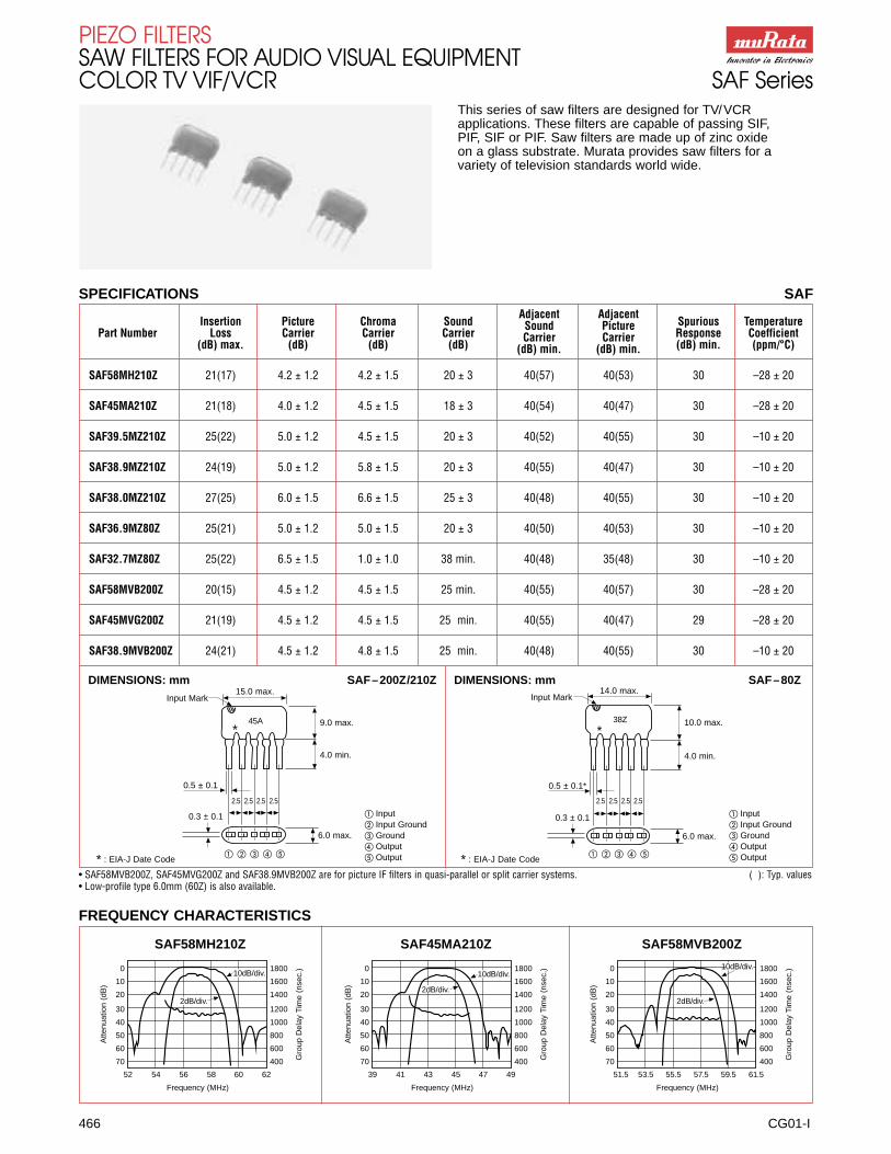
466 CG01-I
PIEZO FILTERSSAW FILTERS FOR AUDIO VISUAL EQUIPMENTCOLOR TV VIF/VCR SAF Series
This series of saw filters are designed for TV/VCR applications. These filters are capable of passing SIF, PIF, SIF or PIF. Saw filters are made up of zinc oxide on a glass substrate. Murata provides saw filters for avariety of television standards world wide.
SPECIFICATIONS SAF
Insertion Picture Chroma SoundAdjacent Adjacent
Spurious TemperaturePart Number Loss Carrier Carrier Carrier
Sound PictureResponse Coefficient
(dB) max. (dB) (dB) (dB)Carrier Carrier
(dB) min. (ppm/°C)(dB) min. (dB) min.
SAF58MH210Z 21(17) 4.2 ± 1.2 4.2 ± 1.5 20 ± 3 40(57) 40(53) 30 –28 ± 20
SAF45MA210Z 21(18) 4.0 ± 1.2 4.5 ± 1.5 18 ± 3 40(54) 40(47) 30 –28 ± 20
SAF39.5MZ210Z 25(22) 5.0 ± 1.2 4.5 ± 1.5 20 ± 3 40(52) 40(55) 30 –10 ± 20
SAF38.9MZ210Z 24(19) 5.0 ± 1.2 5.8 ± 1.5 20 ± 3 40(55) 40(47) 30 –10 ± 20
SAF38.0MZ210Z 27(25) 6.0 ± 1.5 6.6 ± 1.5 25 ± 3 40(48) 40(55) 30 –10 ± 20
SAF36.9MZ80Z 25(21) 5.0 ± 1.2 5.0 ± 1.5 20 ± 3 40(50) 40(53) 30 –10 ± 20
SAF32.7MZ80Z 25(22) 6.5 ± 1.5 1.0 ± 1.0 38 min. 40(48) 35(48) 30 –10 ± 20
SAF58MVB200Z 20(15) 4.5 ± 1.2 4.5 ± 1.5 25 min. 40(55) 40(57) 30 –28 ± 20
SAF45MVG200Z 21(19) 4.5 ± 1.2 4.5 ± 1.5 25 min. 40(55) 40(47) 29 –28 ± 20
SAF38.9MVB200Z 24(21) 4.5 ± 1.2 4.8 ± 1.5 25 min. 40(48) 40(55) 30 –10 ± 20
DIMENSIONS: mm SAF–200Z/210Z DIMENSIONS: mm SAF–80Z
FREQUENCY CHARACTERISTICS
• SAF58MVB200Z, SAF45MVG200Z and SAF38.9MVB200Z are for picture IF filters in quasi-parallel or split carrier systems. ( ): Typ. values• Low-profile type 6.0mm (60Z) is also available.
15.0 max.
45A 9.0 max.
4.0 min.
6.0 max.
0.5 ± 0.1
0.3 ± 0.1
� � � � �
2.52.52.52.5
*
� Input� Input Ground� Ground� Output� Output
14.0 max.
38Z 10.0 max.
4.0 min.
6.0 max.
0.5 ± 0.1*
0.3 ± 0.1
� � � � �
2.52.52.52.5
*
Input MarkInput Mark
SAF58MH210Z SAF45MA210Z SAF58MVB200Z
10dB/div.
2dB/div.
52 54 56 58 60 62
Frequency (MHz)
Atte
nuat
ion
(dB
)
0
10
20
30
40
50
60
70
1800
1600
1400
1200
1000
800
600
400 Gro
up D
elay
Tim
e (n
sec.
)
10dB/div.
2dB/div.
39 41 43 45 47 49
Frequency (MHz)
Atte
nuat
ion
(dB
)
0
10
20
30
40
50
60
70
1800
1600
1400
1200
1000
800
600
400 Gro
up D
elay
Tim
e (n
sec.
) 10dB/div.
2dB/div.
51.5 53.5 55.5 57.5 59.5 61.5
Frequency (MHz)
Atte
nuat
ion
(dB
)
0
10
20
30
40
50
60
70
1800
1600
1400
1200
1000
800
600
400 Gro
up D
elay
Tim
e (n
sec.
)
* : EIA-J Date Code
� Input� Input Ground� Ground� Output� Output* : EIA-J Date Code
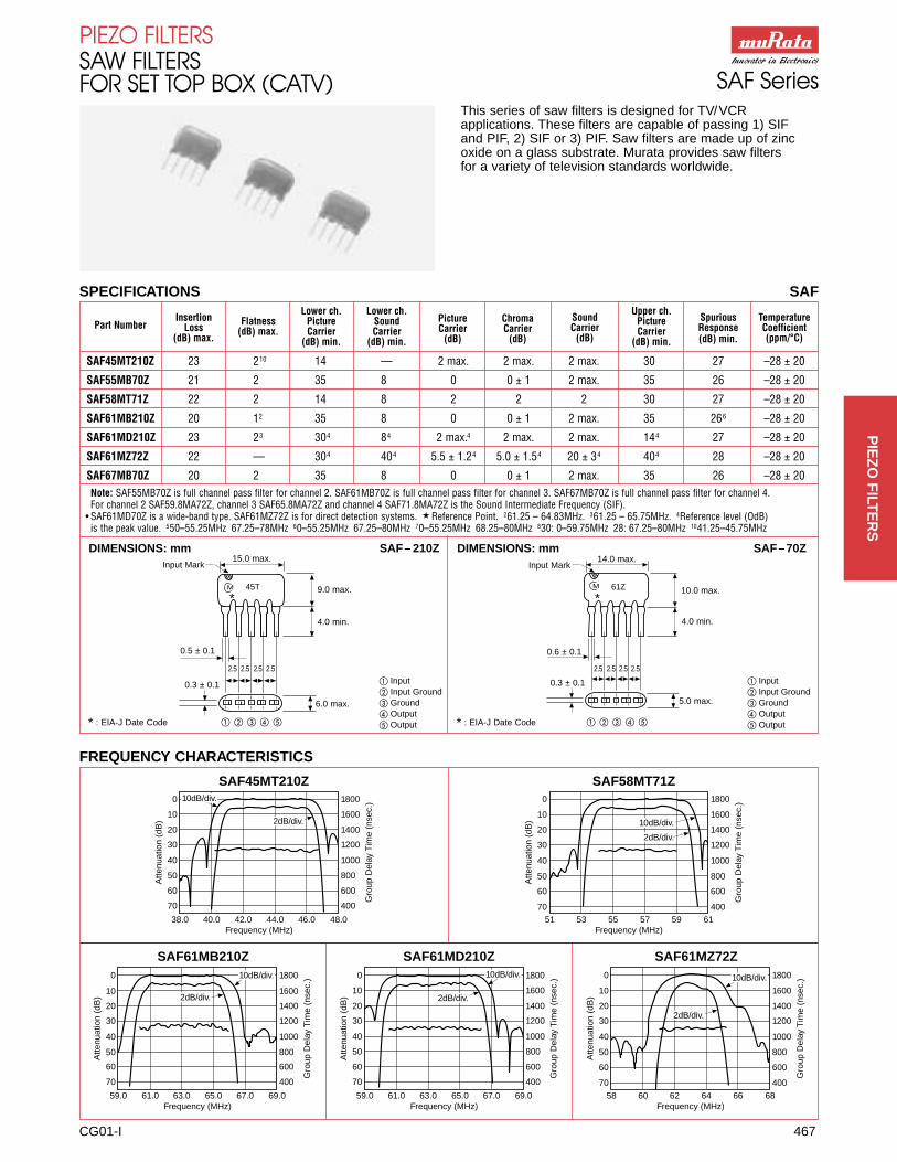
PIEZO FILTERSSAW FILTERSFOR SET TOP BOX (CATV) SAF Series
This series of saw filters is designed for TV/VCR applications. These filters are capable of passing 1) SIF and PIF, 2) SIF or 3) PIF. Saw filters are made up of zincoxide on a glass substrate. Murata provides saw filters for a variety of television standards worldwide.
SPECIFICATIONS SAF
InsertionLower ch. Lower ch.
Picture Chroma SoundUpper ch.
Spurious TemperaturePart Number Loss
Flatness Picture SoundCarrier Carrier Carrier
PictureResponse Coefficient
(dB) max.(dB) max. Carrier Carrier
(dB) (dB) (dB)Carrier
(dB) min. (ppm/°C)(dB) min. (dB) min. (dB) min.
SAF45MT210Z 23 210 14 — 2 max. 2 max. 2 max. 30 27 –28 ± 20
SAF55MB70Z 21 2 35 8 0 0 ± 1 2 max. 35 26 –28 ± 20
SAF58MT71Z 22 2 14 8 2 2 2 30 27 –28 ± 20
SAF61MB210Z 20 12 35 8 0 0 ± 1 2 max. 35 266 –28 ± 20
SAF61MD210Z 23 23 304 84 2 max.4 2 max. 2 max. 144 27 –28 ± 20
SAF61MZ72Z 22 — 304 404 5.5 ± 1.24 5.0 ± 1.54 20 ± 34 404 28 –28 ± 20
SAF67MB70Z 20 2 35 8 0 0 ± 1 2 max. 35 26 –28 ± 20Note: SAF55MB70Z is full channel pass filter for channel 2. SAF61MB70Z is full channel pass filter for channel 3. SAF67MB70Z is full channel pass filter for channel 4. For channel 2 SAF59.8MA72Z, channel 3 SAF65.8MA72Z and channel 4 SAF71.8MA72Z is the Sound Intermediate Frequency (SIF).
• SAF61MD70Z is a wide-band type. SAF61MZ72Z is for direct detection systems. � Reference Point. 261.25 – 64.83MHz. 361.25 – 65.75MHz. 4Reference level (OdB) is the peak value. 550–55.25MHz 67.25–78MHz 60–55.25MHz 67.25–80MHz 70–55.25MHz 68.25–80MHz 830: 0–59.75MHz 28: 67.25–80MHz 1041.25–45.75MHz
DIMENSIONS: mm SAF– 210Z DIMENSIONS: mm SAF–70Z
SAF45MT210Z SAF58MT71Z
SAF61MB210Z SAF61MD210Z SAF61MZ72Z
FREQUENCY CHARACTERISTICS
15.0 max.
45T 9.0 max.
4.0 min.
6.0 max.
0.5 ± 0.1
0.3 ± 0.1
� � � � �
2.52.52.52.5
*
* : EIA-J Date Code
14.0 max.
61Z 10.0 max.
4.0 min.
5.0 max.
0.6 ± 0.1
0.3 ± 0.1
� � � � �
2.52.52.52.5
*
� Input� Input Ground� Ground� Output� Output* : EIA-J Date Code
� Input� Input Ground� Ground� Output� Output
Input MarkInput Mark
MM
0
10
20
30
40
50
60
70
1800
1600
1400
1200
1000
800
600
400
59.0 61.0 63.0 65.0 67.0 69.0Frequency (MHz)
Atte
nuat
ion
(dB
)
Gro
up D
elay
Tim
e (n
sec.
)10dB/div.
2dB/div.
0
10
20
30
40
50
60
70
1800
1600
1400
1200
1000
800
600
400
59.0 61.0 63.0 65.0 67.0 69.0Frequency (MHz)
Atte
nuat
ion
(dB
)
Gro
up D
elay
Tim
e (n
sec.
)10dB/div.
2dB/div.
0
10
20
30
40
50
60
70
1800
1600
1400
1200
1000
800
600
400
58 60 62 64 66 68Frequency (MHz)
Atte
nuat
ion
(dB
)
Gro
up D
elay
Tim
e (n
sec.
)10dB/div.
2dB/div.
0
10
20
30
40
50
60
70
1800
1600
1400
1200
1000
800
600
400
38.0 40.0 42.0 44.0 46.0 48.0Frequency (MHz)
Atte
nuat
ion
(dB
)
Gro
up D
elay
Tim
e (n
sec.
)10dB/div.
2dB/div.
0
10
20
30
40
50
60
70
1800
1600
1400
1200
1000
800
600
40051 53 55 57 59 61
Frequency (MHz)
Atte
nuat
ion
(dB
)
Gro
up D
elay
Tim
e (n
sec.
)
10dB/div.
2dB/div.
CG01-I 467
PIE
ZO
FILT
ER
S
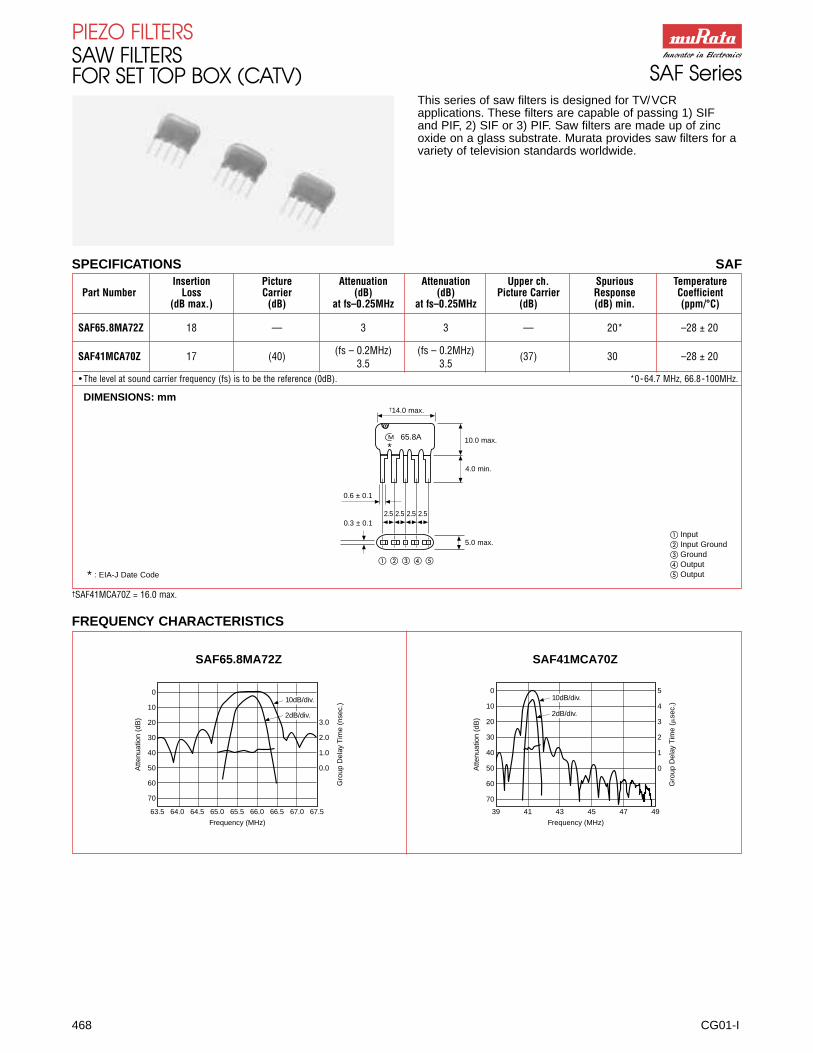
468 CG01-I
PIEZO FILTERSSAW FILTERSFOR SET TOP BOX (CATV) SAF Series
This series of saw filters is designed for TV/VCR applications. These filters are capable of passing 1) SIF and PIF, 2) SIF or 3) PIF. Saw filters are made up of zincoxide on a glass substrate. Murata provides saw filters for avariety of television standards worldwide.
SPECIFICATIONS SAF
SAF65.8MA72Z SAF41MCA70Z
0
10
20
30
40
50
60
70
2.0
1.0
0.0
63.5 64.0 64.5 65.0 67.0 67.5
Frequency (MHz)
Atte
nuat
ion
(dB
)
Gro
up D
elay
Tim
e (n
sec.
)10dB/div.
2dB/div.3.0
65.5 66.0 66.5
0
10
20
30
40
50
60
70
5
4
3
2
1
0
39 41 43 45 47 49
Frequency (MHz)
Atte
nuat
ion
(dB
)
Gro
up D
elay
Tim
e (�
sec.
)
10dB/div.
2dB/div.
FREQUENCY CHARACTERISTICS
Insertion Picture Attenuation Attenuation Upper ch. Spurious TemperaturePart Number Loss Carrier (dB) (dB) Picture Carrier Response Coefficient
(dB max.) (dB) at fs–0.25MHz at fs–0.25MHz (dB) (dB) min. (ppm/°C)
SAF65.8MA72Z 18 — 3 3 — 20* –28 ± 20
SAF41MCA70Z 17 (40) (fs – 0.2MHz) (fs – 0.2MHz) (37) 30 –28 ± 203.5 3.5
• The level at sound carrier frequency (fs) is to be the reference (0dB). *0-64.7 MHz, 66.8-100MHz.
DIMENSIONS: mm
* : EIA-J Date Code
†14.0 max.
10.0 max.
4.0 min.
5.0 max.
0.6 ± 0.1
0.3 ± 0.12.5 2.5 2.5 2.5
*
� � � � �
� Input� Input Ground� Ground� Output� Output
M 65.8A
†SAF41MCA70Z = 16.0 max.

Part Number SAF44MTC80ZL SAF44.00MTD220ZL SAF44.00MTE220ZL
Insertion Loss(at 44.00 MHz)
22.0dB 20.5dB 21.0dB
39.75MHZ 35.0 min. — —40.00MHZ — 32.0 min. 32.0 min.40.50MHZ — 10.0 min. 7.0 min.41.00MHZ — 3.5 ± 1.5 1.5 ± 1.541.31MHZ 0.7 ± 1.3 — —
Amplitude 41.47MHZ — 0.0 ± 1.2 0.0 ± 1.2Response 46.53MHZ — 0.0 ± 1.2 0.0 ± 1.2
dB 46.69MHZ 1.5 ± 1.5 — —47.00MHZ — 3.5 ± 1.5 2.0 ± 1.547.25MHZ 25.0 min. — —47.50MHZ — 10.0 min. 8.0 min.48.00MHZ — 34.0 min. 30.0 min.
1.0dB p-p 1.0dB p-p 1.0dB p-pAmplitude Ripple(41.62 to 46.38MHz) (41.00 to 47.00MHz) (41.00 to 47.00MHz)
60 nsec. max. 60 nsec. p-p max. 60 nsec. p-p max. GDT Ripple(41.62 to 46.38MHz) (41.00 to 47.00MHz) (41.00 to 47.00MHz)
Spurious Responce (dB min.) 30.00 (0.00 to 40.00MHz) 30.0 (35.00 to 40.00MHz) 28.00 (0.00 to 40.00MHz)(Reference Level at 44.00MHz) 30.00 (48.00 to 55.00MHz) 28.0 (48.00 to 55.00MHz) 25.00 (48.00 to 55.00MHz)
DIMENSIONS: mm SAF–80Z DIMENSIONS: mm SAF–220Z
TEST CIRCUIT
CG01-I 469
PIEZO FILTERSSAW FILTERS FOR CABLE MODEMDTV/DIGITAL CATV SAF Series
To meet the needs of the newest emerging technologies,Murata now offers a line of SAW filters designed for DigitalTelevision, Digital Cable Television, and Cable Modemapplications.
SPECIFICATIONS SAF MHz
15.0 max.
9.0 max.
5.0 ± 1.0
6.0 max.
0.5 ± 0.1
0.3 ± 0.1
� � � � �
2.52.52.52.5
*
� Input� Input Ground� Ground� Output� Output
� Input� Input Ground� Ground� Output� Output
Input MarkInput Mark16.0 max.
10.0 max.
5.0 ± 1.0
6.0 max.
0.5 ± 0.1
0.3 ± 0.1
� � � � �
*MM
* : EIA-J Date Code * : EIA-J Date Code
NEW
SAF44MTC80ZL SAF44.00MTD(E)220Z6
Rout: 2.0k� Rout: 3.0k�
Rout: 1.7�H Lout: 1.55�H
� � � � � � �
� � � � � �
Lout
R out
S.S.G.–30dBm max.
75�
100�
0.01�F
75�
RF Voltmeter
0.01�F 0.01�F
2k�
1k�
+B=12• 0.05V
7A7607AP
2.5
±0.
2
2.5
±0.
2
2.5
±0.
2
2.5
±0.
2
PIE
ZO
FILT
ER
S
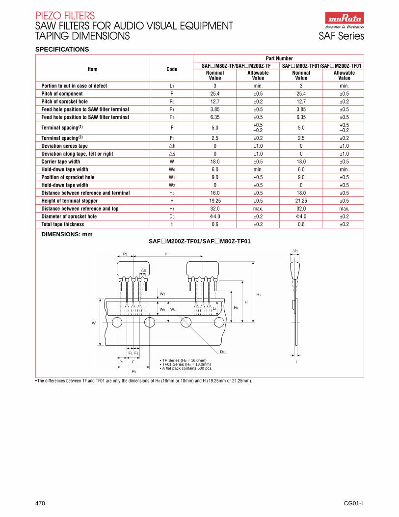
470 CG01-I
PIEZO FILTERSSAW FILTERS FOR AUDIO VISUAL EQUIPMENTTAPING DIMENSIONS SAF SeriesSPECIFICATIONS
Part NumberSAF�M80Z-TF/SAF�M200Z-TF SAF�M80Z-TF01/SAF�M200Z-TF01
Item CodeNominal Allowable Nominal Allowable
Value Value Value ValuePortion to cut in case of defect L1 3 min. 3 min.Pitch of component P 25.4 ±0.5 25.4 ±0.5Pitch of sprocket hole P0 12.7 ±0.2 12.7 ±0.2Feed hole position to SAW filter terminal P1 3.85 ±0.5 3.85 ±0.5Feed hole position to SAW filter terminal P2 6.35 ±0.5 6.35 ±0.5
Terminal spacing(1) F 5.0 +0.5 5.0 +0.5–0.2 –0.2
Terminal spacing(2) F1 2.5 ±0.2 2.5 ±0.2Deviation across tape �h 0 ±1.0 0 ±1.0Deviation along tape, left or right �s 0 ±1.0 0 ±1.0Carrier tape width W 18.0 ±0.5 18.0 ±0.5Hold-down tape width W0 6.0 min. 6.0 min.Position of sprocket hole W1 9.0 ±0.5 9.0 ±0.5Hold-down tape width W2 0 ±0.5 0 ±0.5Distance between reference and terminal H0 16.0 ±0.5 18.0 ±0.5Height of terminal stopper H 19.25 ±0.5 21.25 ±0.5Distance between reference and top H1 32.0 max. 32.0 max.Diameter of sprocket hole D0 �4.0 ±0.2 �4.0 ±0.2Total tape thickness t 0.6 ±0.2 0.6 ±0.2
DIMENSIONS: mmSAF�M200Z-TF01/SAF�M80Z-TF01
P2 P
H0L1
D0
P0
W2
W0 W1
W
P1
F1 F1
F
H
t
H1
�h
�s
• TF Series (H0 = 16.0mm)• TF01 Series (H0 = 18.0mm)• A flat pack contains 500 pcs.
•The differences between TF and TF01 are only the dimensions of H0 (16mm or 18mm) and H (19.25mm or 21.25mm).
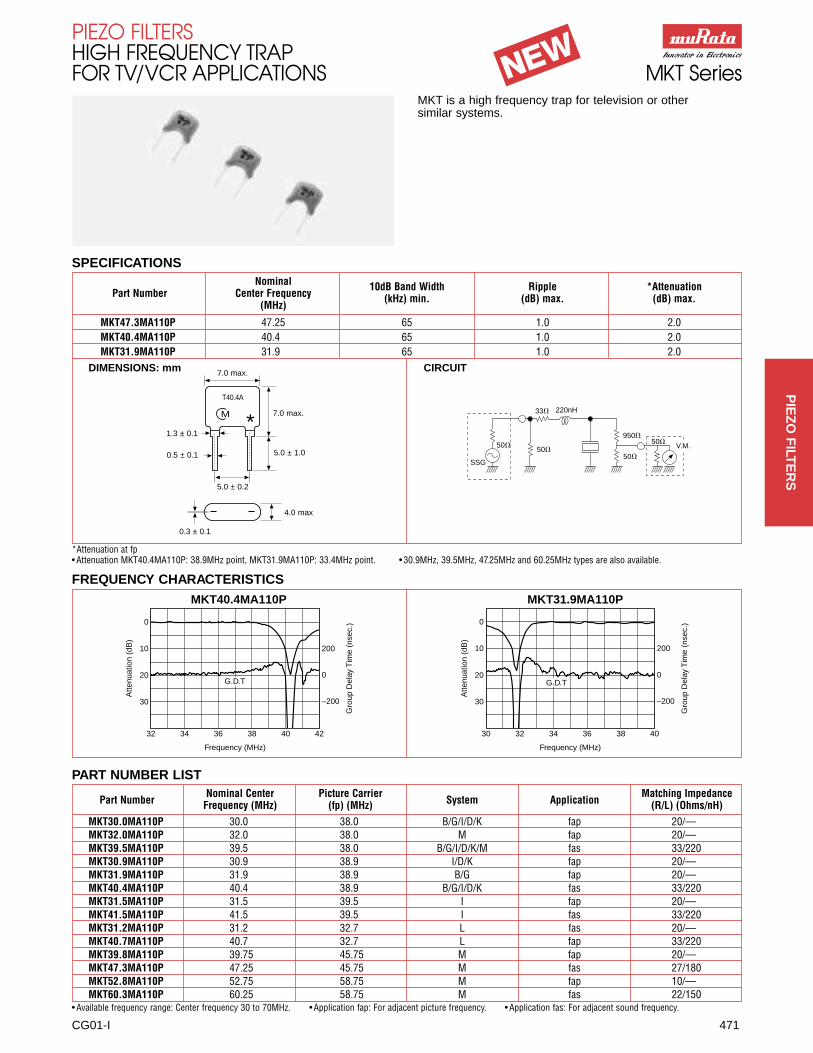
CG01-I 471
PIEZO FILTERSHIGH FREQUENCY TRAP FOR TV/VCR APPLICATIONS MKT Series
MKT is a high frequency trap for television or other similar systems.
SPECIFICATIONSNominal 10dB Band Width Ripple *Attenuation
Part Number Center Frequency (kHz) min. (dB) max. (dB) max.(MHz)
MKT47.3MA110P 47.25 65 1.0 2.0MKT40.4MA110P 40.4 65 1.0 2.0MKT31.9MA110P 31.9 65 1.0 2.0
DIMENSIONS: mm CIRCUIT7.0 max.
MKT40.4MA110P MKT31.9MA110P
FREQUENCY CHARACTERISTICS
T40.4A
7.0 max.
4.0 max
0.3 ± 0.1
5.0 ± 1.0
1.3 ± 0.1
0.5 ± 0.1
5.0 ± 0.2
M
SSG
50�50�
50�
50�V.M.
950�
33� 220nH
*Attenuation at fp• Attenuation MKT40.4MA110P: 38.9MHz point, MKT31.9MA110P: 33.4MHz point. • 30.9MHz, 39.5MHz, 47.25MHz and 60.25MHz types are also available.
• Available frequency range: Center frequency 30 to 70MHz. • Application fap: For adjacent picture frequency. • Application fas: For adjacent sound frequency.
Part NumberNominal Center Picture Carrier
System ApplicationMatching Impedance
Frequency (MHz) (fp) (MHz) (R/L) (Ohms/nH)MKT30.0MA110P 30.0 38.0 B/G/I/D/K fap 20/—MKT32.0MA110P 32.0 38.0 M fap 20/—MKT39.5MA110P 39.5 38.0 B/G/I/D/K/M fas 33/220MKT30.9MA110P 30.9 38.9 I/D/K fap 20/—MKT31.9MA110P 31.9 38.9 B/G fap 20/—MKT40.4MA110P 40.4 38.9 B/G/I/D/K fas 33/220MKT31.5MA110P 31.5 39.5 I fap 20/—MKT41.5MA110P 41.5 39.5 I fas 33/220MKT31.2MA110P 31.2 32.7 L fas 20/—MKT40.7MA110P 40.7 32.7 L fap 33/220MKT39.8MA110P 39.75 45.75 M fap 20/—MKT47.3MA110P 47.25 45.75 M fas 27/180MKT52.8MA110P 52.75 58.75 M fap 10/—MKT60.3MA110P 60.25 58.75 M fas 22/150
PART NUMBER LIST
*
NEW
0
10
20
30
200
0
–200
32 34 36 38 40 42
Frequency (MHz)
Atte
nuat
ion
(dB
)
Gro
up D
elay
Tim
e (n
sec.
)
G.D.T
0
10
20
30
200
0
–200
30 32 34 36 38 40
Frequency (MHz)
Atte
nuat
ion
(dB
)
Gro
up D
elay
Tim
e (n
sec.
)G.D.T
PIE
ZO
FILT
ER
S


![[DESIGN] Piezo-Piezo to Pie](https://cdn.vdocument.in/doc/165x107/5571f8bb49795991698df909/design-piezo-piezo-to-pie.jpg)