Power Electronics Lab
POWER ELECTRONICS LAB
Power Electronics Lab
Sri Vahini institute of science & technology Page 1 Dept Of EEE
LIST OF EXPERIMENTS
S.No Name of the experiment Date Signature
1 Study of Characteristics of SCR, MOSFET &
IGBT
2 Single Phase Half Controlled Converter with R
and RL load
3 Single Phase Fully Controlled Bridge Converter
with R and RL loads
4 Single Phase AC Voltage Controller with R &
RL Loads
5 Single Phase Cycloconverter with R & RL
Loads
6 Single Phase Series Inverter with R & RL Loads
7 Single Phase Parallel Inverter with R & RL
Loads
8 Gate Firing Circuits for SCR’s
9 Forced Commutation Circuits (Class A, B, C &
D)
10 Single Phase Dual Converter with RL Load
Power Electronics Lab
Sri Vahini institute of science & technology Page 2 Dept Of EEE
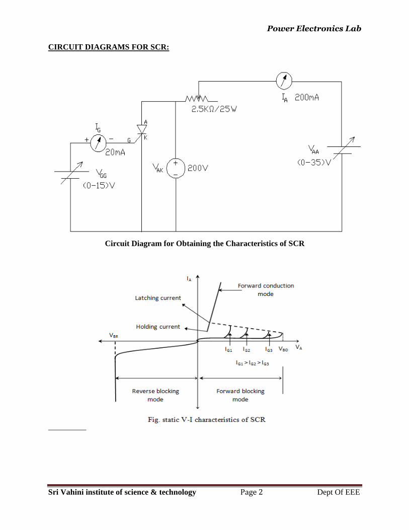
CIRCUIT DIAGRAMS FOR SCR:
Circuit Diagram for Obtaining the Characteristics of SCR
Power Electronics Lab
Sri Vahini institute of science & technology Page 3 Dept Of EEE
STUDY OF CHARACTERISTICS OF SCR, MOSFET & IGBT
AIM: -
To plot the characteristics of SCR, MOSFET & IGBT
APPARATUS: -
S.no Description Quantity
1 Characteristics Kit 1
2 Ammeter (0-200)mA 2
3 Voltmeter (0-20)V 2
4 RPS (0-30)V,2A 1
PROCEDURE: To obtain Characteristics of SCR:
1. The connections are made as per circuit diagram. 2. Switch on the regulated power supply. Apply 10V across anode & cathode of
SCR. 3. Gradually increase the gate current till the SCR becomes ON. Note down VAK, IA. 4. Now increase supply voltage gradually and IA are noted for three or four readings. 5. Steps 3 to 4 are repeated for another values of VAK say 20V. 6. Tabulate the readings in the table. 7. Plot a graph of VAK versus IA. 8. To determine Holding current IH :
i) Keep proper VAK to trigger SCR by gate current. Trigger SCR by applying gate current .Keep sufficient load current by varying load resistance in fully clock wise direction.
ii) To open gate circuit, now reduce load current till SCR jump to blocking state.
iii) The minimum current for which SCR suspend under ON condition is noted which is Holding current IH.
9. Latching current is 1.5 to 2 times of holding current value
Power Electronics Lab
Sri Vahini institute of science & technology Page 4 Dept Of EEE
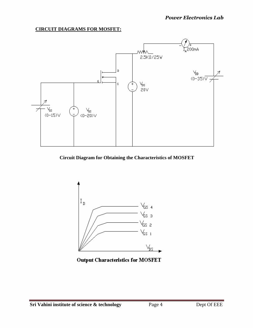
CIRCUIT DIAGRAMS FOR MOSFET:
Circuit Diagram for Obtaining the Characteristics of MOSFET

Power Electronics Lab
Sri Vahini institute of science & technology Page 5 Dept Of EEE
To obtain Characteristics of MOSFET:
Output Characteristics: 1. The connections are made as per circuit diagram
2. Switch on the equipment. Keep VDS say 10V, vary VGS note down the range of VGS for which drain current is varying for constant VGS.
3. Keep VGS constant, (VGS must be within the range determined by step 2). 4. Vary VDS in steps, note down corresponding ID. 5. Step 4 is repeated for different values of VGS. 6. Tabulate the readings in the table. 7. Plot a graph of ID against VDS for different VGS.
Transfer Characteristics:
1.The connections are made as per circuit diagram 2. Switch on the equipment. Keep VDS say 10V, vary VGS in steps ,note down the
corresponding drain current ID. 3. Tabulate the readings in the table. 4. Plot a graph of ID against VGS.
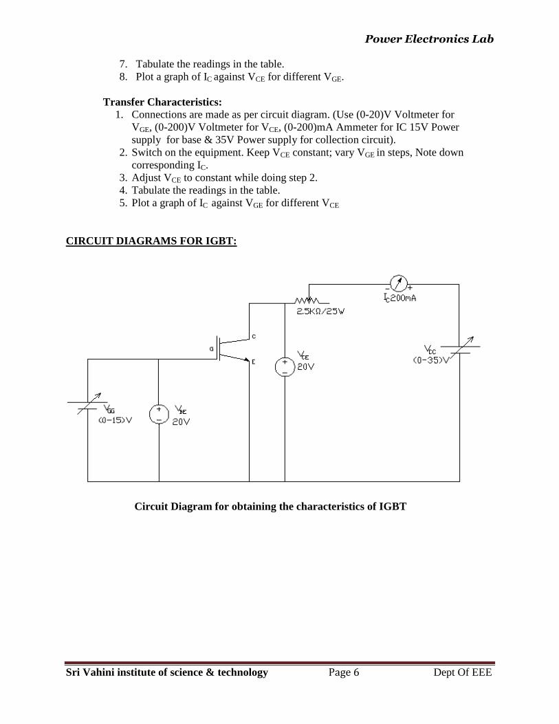
To obtain Characteristics of IGBT:
Output Characteristics: 1. Connections are made as per circuit diagram.(Use 20V Voltmeter for VGE ,
200V Voltmeter for VCE , 200 ma Ammeter for IC 15V Power supply for base & 35V Power supply for collection circuit).
2. Switch on the equipment .Keep VCE 10V, vary VGE note down the range of VGE for which collector current is varying for constant VCE.
3. Keep VGE constant,(VGE must be with in the range determined by step 2). 4. Vary VCE in steps, note down the corresponding IC. 5. Adjust VGE to constant while doing step 4. 6. Step 4 is repeated for different VGE.
Power Electronics Lab
Sri Vahini institute of science & technology Page 6 Dept Of EEE
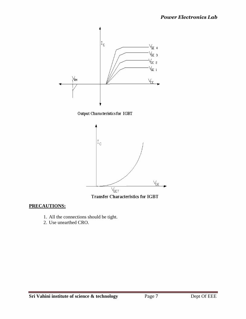
7. Tabulate the readings in the table. 8. Plot a graph of IC against VCE for different VGE.
Transfer Characteristics:
1. Connections are made as per circuit diagram. (Use (0-20)V Voltmeter for VGE, (0-200)V Voltmeter for VCE, (0-200)mA Ammeter for IC 15V Power supply for base & 35V Power supply for collection circuit).
2. Switch on the equipment. Keep VCE constant; vary VGE in steps, Note down corresponding IC.
3. Adjust VCE to constant while doing step 2. 4. Tabulate the readings in the table. 5. Plot a graph of IC against VGE for different VCE
CIRCUIT DIAGRAMS FOR IGBT:
Circuit Diagram for obtaining the characteristics of IGBT
Power Electronics Lab
Sri Vahini institute of science & technology Page 7 Dept Of EEE
PRECAUTIONS:
1. All the connections should be tight. 2. Use unearthed CRO.
Power Electronics Lab
Sri Vahini institute of science & technology Page 8 Dept Of EEE
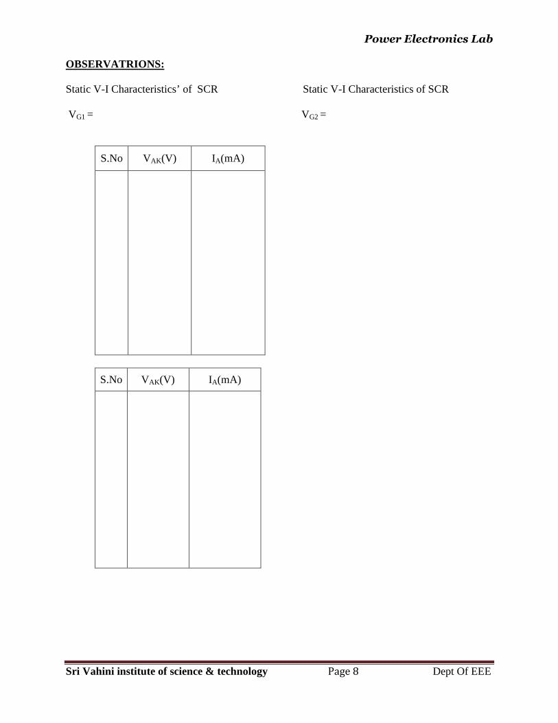
OBSERVATRIONS: Static V-I Characteristics’ of SCR Static V-I Characteristics of SCR VG1 = VG2 =
S.No VAK(V) IA(mA)
S.No VAK(V) IA(mA)
Power Electronics Lab
Sri Vahini institute of science & technology Page 9 Dept Of EEE
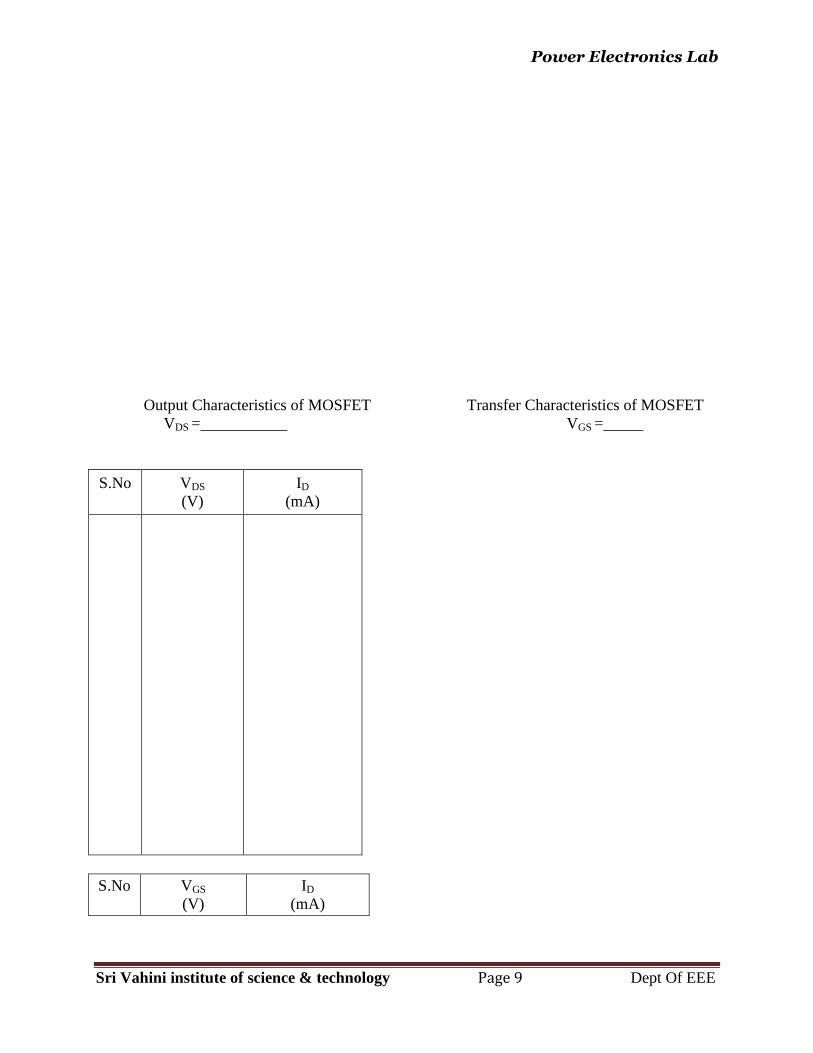
Output Characteristics of MOSFET Transfer Characteristics of MOSFET
VDS = VGS =
S.No
VDS
(V) ID
(mA)
S.No
VGS
(V) ID
(mA)
Power Electronics Lab
Sri Vahini institute of science & technology Page 10 Dept Of EEE
Power Electronics Lab
Sri Vahini institute of science & technology Page 11 Dept Of EEE
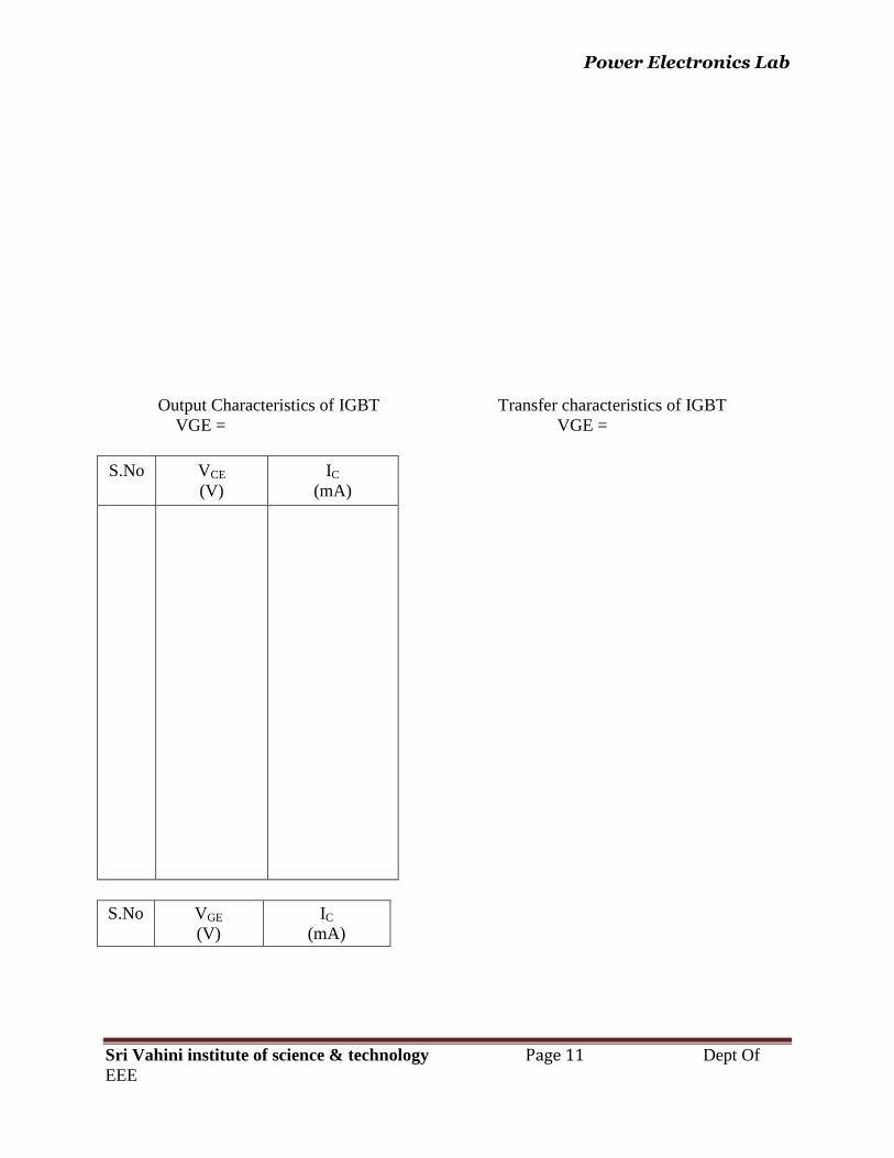
Output Characteristics of IGBT Transfer characteristics of IGBT VGE = VGE =
S.No
VCE
(V) IC
(mA)
S.No
VGE
(V) IC
(mA)
Power Electronics Lab
Sri Vahini institute of science & technology Page 12 Dept Of EEE
RESULT:
Power Electronics Lab
Sri Vahini institute of science & technology Page 13 Dept Of EEE
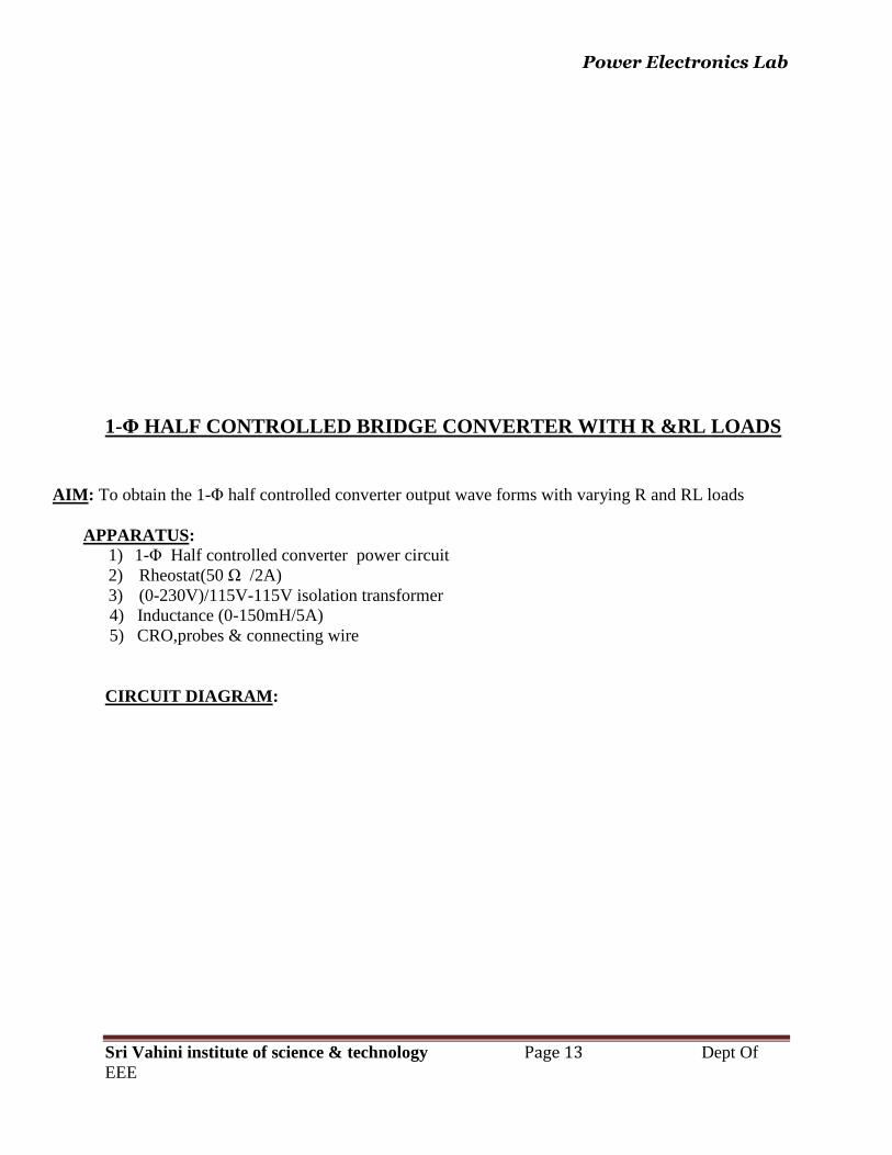
1-Φ HALF CONTROLLED BRIDGE CONVERTER WITH R &RL LOADS
AIM : To obtain the 1-Φ half controlled converter output wave forms with varying R and RL loads APPARATUS:
1) 1-Φ Half controlled converter power circuit 2) Rheostat(50 Ω /2A) 3) (0-230V)/115V-115V isolation transformer 4) Inductance (0-150mH/5A) 5) CRO,probes & connecting wire
CIRCUIT DIAGRAM :
Power Electronics Lab
Sri Vahini institute of science & technology Page 14 Dept Of EEE
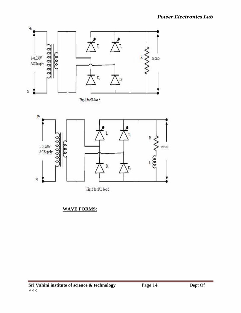
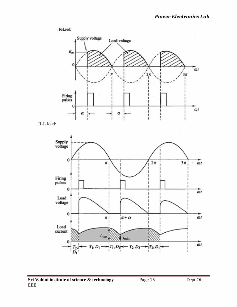
WAVE FORMS:
Power Electronics Lab
Sri Vahini institute of science & technology Page 15 Dept Of EEE
R-L load:
Power Electronics Lab
Sri Vahini institute of science & technology Page 16 Dept Of EEE
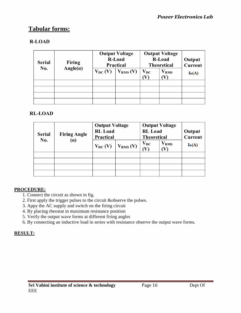
Tabular forms:
PROCEDURE: 1. Connect the circuit as shown in fig. 2. First apply the trigger pulses to the circuit &observe the pulses. 3. Appy the AC supply and switch on the firing circuit 4. By placing rheostat in maximum resistance position 5. Verify the output wave forms at different firing angles 6. By connecting an inductive load in series with resistance observe the output wave forms. RESULT:
Power Electronics Lab
Sri Vahini institute of science & technology Page 17 Dept Of EEE
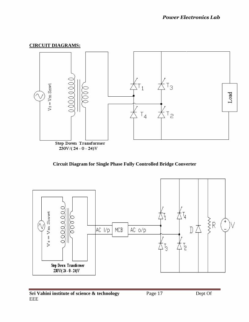
CIRCUIT DIAGRAMS:
Circuit Diagram for Single Phase Fully Controlled Bridge Converter
Power Electronics Lab
Sri Vahini institute of science & technology Page 18 Dept Of EEE
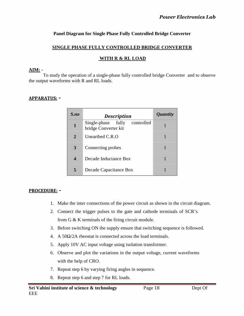
Panel Diagram for Single Phase Fully Controlled Bridge Converter
SINGLE PHASE FULLY CONTROLLED BRIDGE CONVERTER
WITH R & RL LOAD
AIM: -
To study the operation of a single-phase fully controlled bridge Converter and to observe the output waveforms with R and RL loads.
APPARATUS: -
S.no Description Quantity
1 Single-phase fully controlled bridge Converter kit
1
2 Unearthed C.R.O 1
3 Connecting probes 1
4 Decade Inductance Box 1
5 Decade Capacitance Box 1
PROCEDURE: -
1. Make the inter connections of the power circuit as shown in the circuit diagram.
2. Connect the trigger pulses to the gate and cathode terminals of SCR’s
from G & K terminals of the firing circuit module.
3. Before switching ON the supply ensure that switching sequence is followed.
4. A 50Ω/2A rheostat is connected across the load terminals.
5. Apply 10V AC input voltage using isolation transformer.
6. Observe and plot the variations in the output voltage, current waveforms
with the help of CRO.
7. Repeat step 6 by varying firing angles in sequence.
8. Repeat step 6 and step 7 for RL loads.
Power Electronics Lab
Sri Vahini institute of science & technology Page 19 Dept Of EEE
9. Also observe waveforms by connecting firing wheeling diode & by using
half controlled converter.
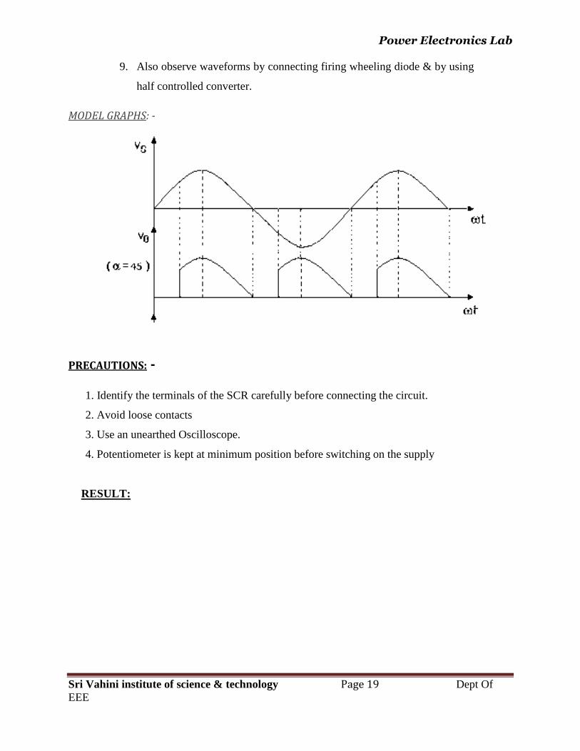
MODEL GRAPHS: -
PRECAUTIONS: -
1. Identify the terminals of the SCR carefully before connecting the circuit.
2. Avoid loose contacts
3. Use an unearthed Oscilloscope.
4. Potentiometer is kept at minimum position before switching on the supply
RESULT:
Power Electronics Lab
Sri Vahini institute of science & technology Page 20 Dept Of EEE
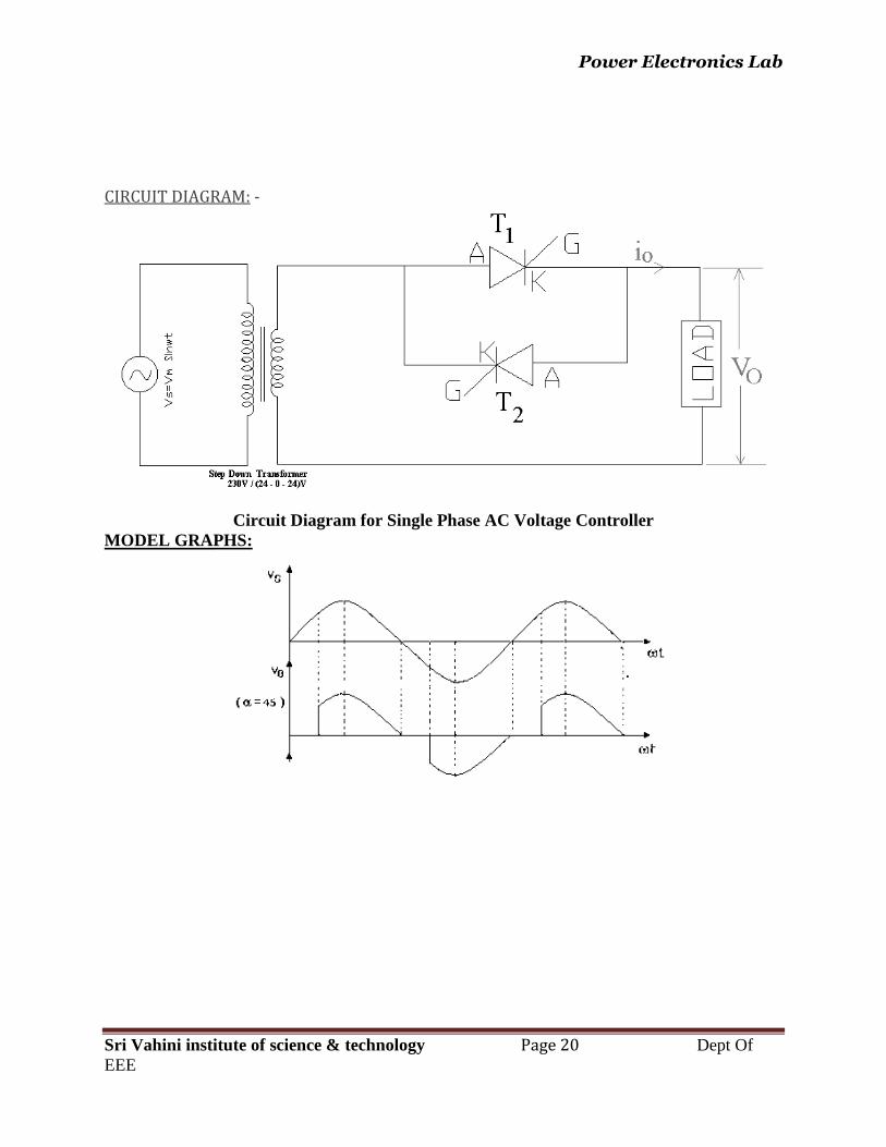
CIRCUIT DIAGRAM: -
Circuit Diagram for Single Phase AC Voltage Controller MODEL GRAPHS:
Power Electronics Lab
Sri Vahini institute of science & technology Page 21 Dept Of EEE
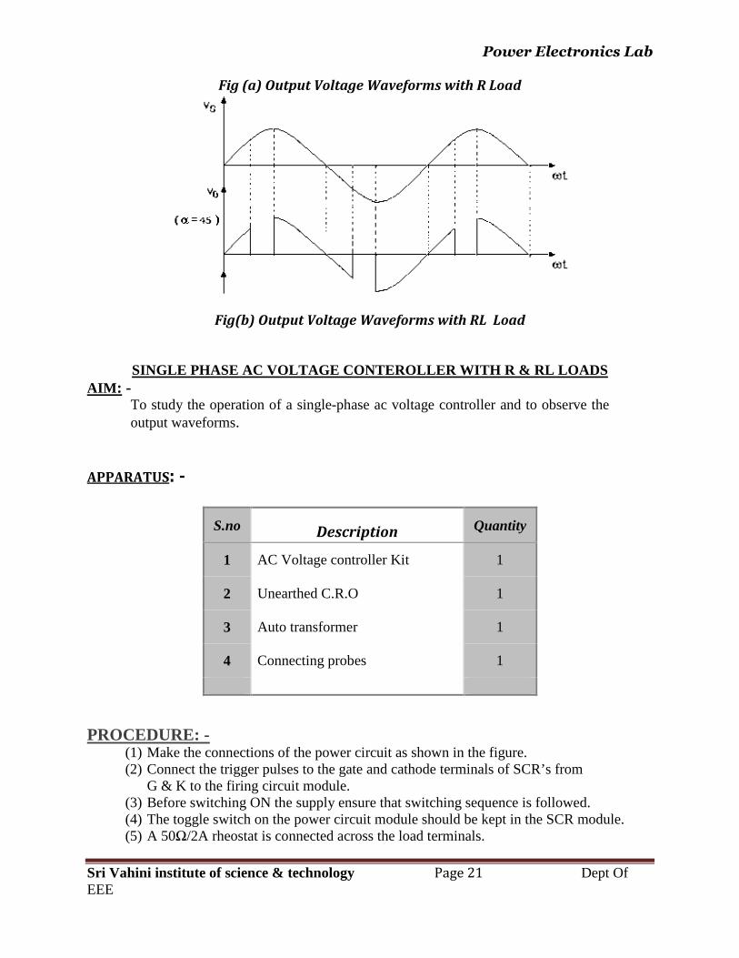
Fig (a) Output Voltage Waveforms with R Load
Fig(b) Output Voltage Waveforms with RL Load
SINGLE PHASE AC VOLTAGE CONTEROLLER WITH R & RL LOA DS AIM : -
To study the operation of a single-phase ac voltage controller and to observe the output waveforms.
APPARATUS: -
S.no Description Quantity
1 AC Voltage controller Kit 1
2 Unearthed C.R.O 1
3 Auto transformer 1
4 Connecting probes 1
PROCEDURE: - (1) Make the connections of the power circuit as shown in the figure. (2) Connect the trigger pulses to the gate and cathode terminals of SCR’s from
G & K to the firing circuit module. (3) Before switching ON the supply ensure that switching sequence is followed. (4) The toggle switch on the power circuit module should be kept in the SCR module. (5) A 50Ω/2A rheostat is connected across the load terminals.
Power Electronics Lab
Sri Vahini institute of science & technology Page 22 Dept Of EEE
(6) Switch ON the step down transformer supply. (7) Trigger SCR’s, observe firing pulses & plot output voltage across load, currents
waveforms with the help of CRO . (8) Now repeat step 6 for R L loads.
PRECAUTIONS:
1. Identify the terminals of the SCR carefully before connecting the circuit 2. Use unearthed CRO 3. Disconnect all the circuit before going for next experiment. 4. Before switching on the supply see that the firing angle knob & the auto transformer are in minimum position. RESULT:
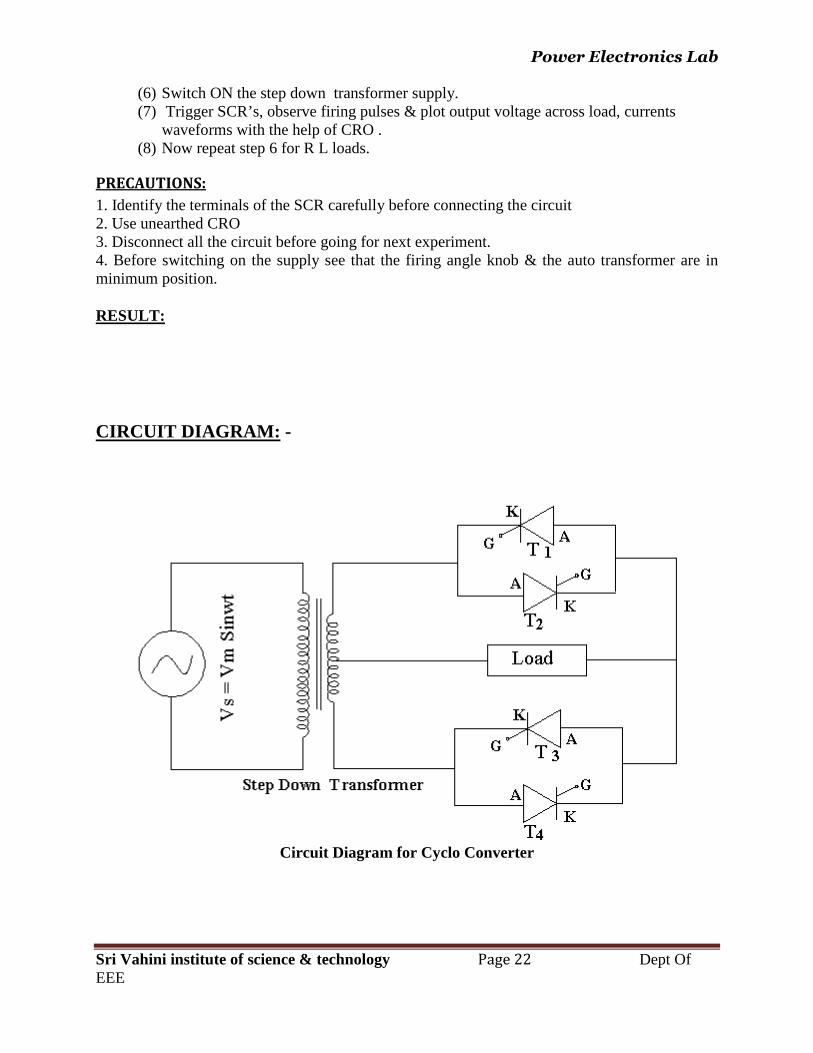
CIRCUIT DIAGRAM: -
Circuit Diagram for Cyclo Converter
Power Electronics Lab
Sri Vahini institute of science & technology Page 23 Dept Of EEE
SINGLE PHASE CYCLOCONVERTER WITH R & RL LOADS
AIM:
To study the operation of single phase cyclo converter and to observe output waveforms.
APPARATUS: -
S.no Description Quantity
1 Single-phase Cycloconverters kit 1
2 Unearthed C.R.O 1
3 Connecting probes 1
PROCEDURE: - 1. Keep SW1 in off position. 2. Connect C.R.O across the load terminal see that load negative terminal and main ground
are isolated through optoisolators. Keep vertical amplifier sensitivity in 10 volts/div.position.
3. Switch ON main supply. Take SW1 to divide by 2,3 and 4 positions and observe the output waveform by properly adjusting the time division switch on the time sweep controls of C.R.O.
Power Electronics Lab
Sri Vahini institute of science & technology Page 24 Dept Of EEE
4. Now Keep SW1 to position of divide by 2. Take the C.R.O terminals to the logic gate site. Connect the C.R.O negative terminal to the main ground and live input terminal to the binding posts marked in 1,2,3,4 etc for observation of the waveforms. Note down these waveforms.
5. Repeat the steps (4) for divide by 3 and divide by 4 positions of SW1. PRECAUTIONS:
1. The frequency variable knob is kept at zero before switching ON the supply. 2. Use an unearthed CRO.
RESULT: -
CIRCUIT DIAGRAM:
Power Electronics Lab
Sri Vahini institute of science & technology Page 25 Dept Of EEE
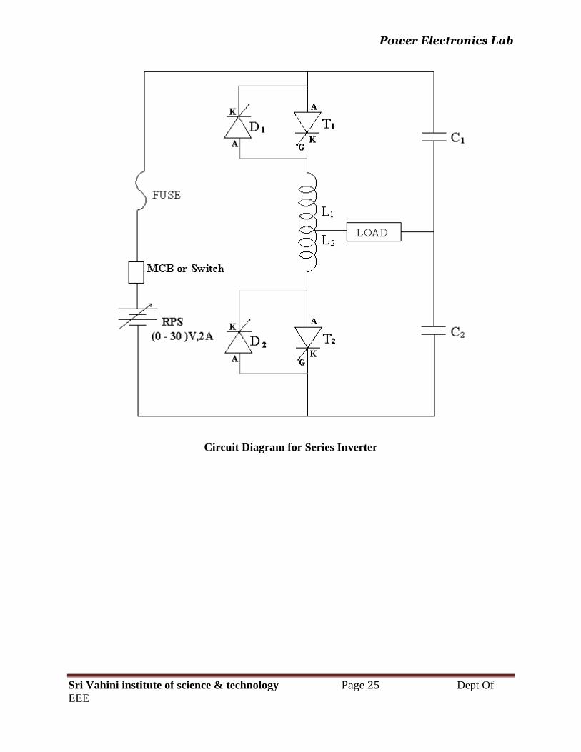
Circuit Diagram for Series Inverter
Power Electronics Lab
Sri Vahini institute of science & technology Page 26 Dept Of EEE
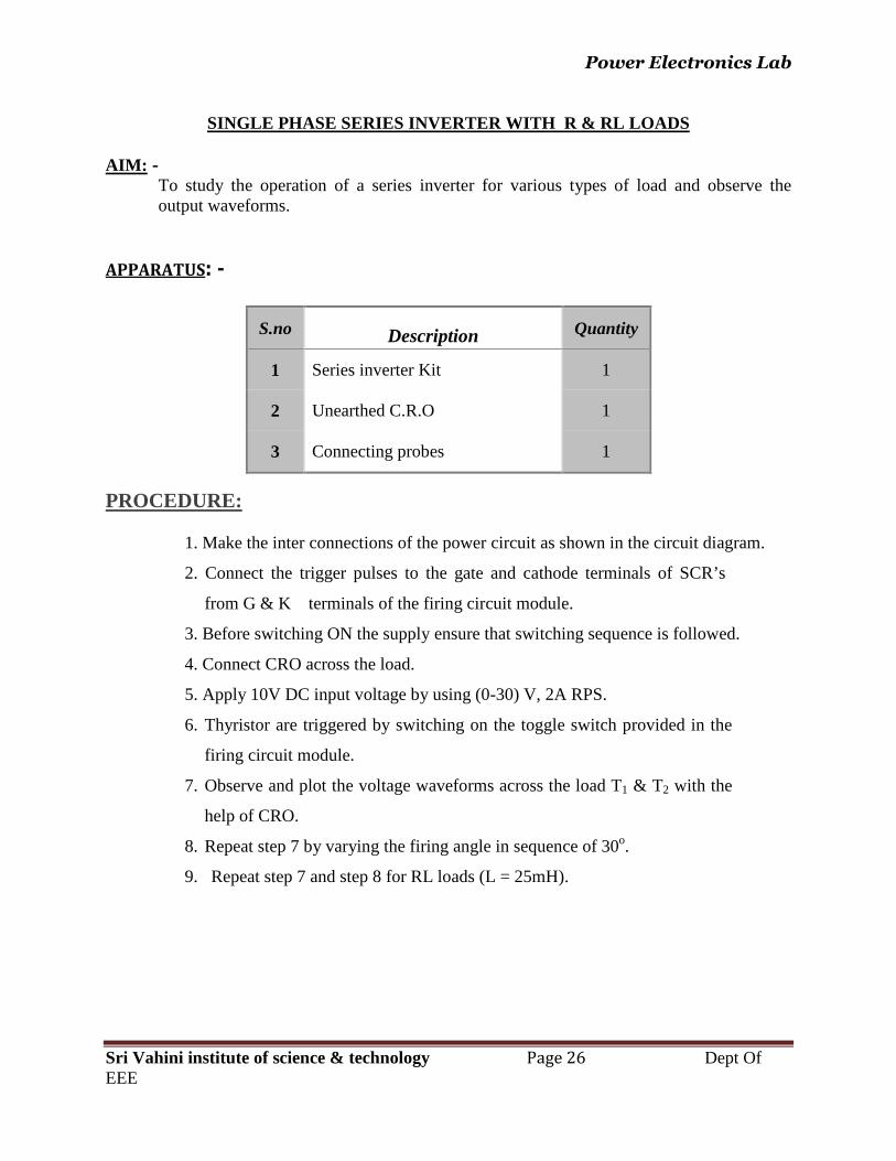
SINGLE PHASE SERIES INVERTER WITH R & RL LOADS
AIM: -
To study the operation of a series inverter for various types of load and observe the output waveforms.
APPARATUS: -
S.no Description Quantity
1 Series inverter Kit 1
2 Unearthed C.R.O 1
3 Connecting probes 1
PROCEDURE:
1. Make the inter connections of the power circuit as shown in the circuit diagram.
2. Connect the trigger pulses to the gate and cathode terminals of SCR’s
from G & K terminals of the firing circuit module.
3. Before switching ON the supply ensure that switching sequence is followed.
4. Connect CRO across the load.
5. Apply 10V DC input voltage by using (0-30) V, 2A RPS.
6. Thyristor are triggered by switching on the toggle switch provided in the
firing circuit module.
7. Observe and plot the voltage waveforms across the load T1 & T2 with the
help of CRO.
8. Repeat step 7 by varying the firing angle in sequence of 30o.
9. Repeat step 7 and step 8 for RL loads (L = 25mH).
Power Electronics Lab
Sri Vahini institute of science & technology Page 27 Dept Of EEE
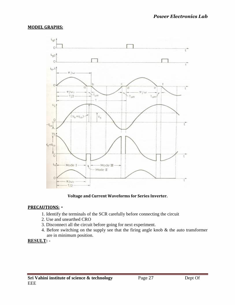
MODEL GRAPHS:
Voltage and Current Waveforms for Series Inverter.
PRECAUTIONS: - 1. Identify the terminals of the SCR carefully before connecting the circuit 2. Use and unearthed CRO 3. Disconnect all the circuit before going for next experiment. 4. Before switching on the supply see that the firing angle knob & the auto transformer
are in minimum position. RESULT: -
Power Electronics Lab
Sri Vahini institute of science & technology Page 28 Dept Of EEE
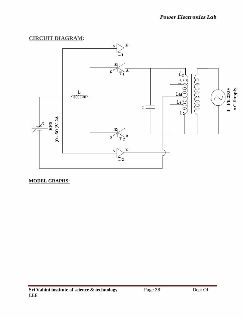
CIRCUIT DIAGRAM :
MODEL GRAPHS:
Power Electronics Lab
Sri Vahini institute of science & technology Page 29 Dept Of EEE
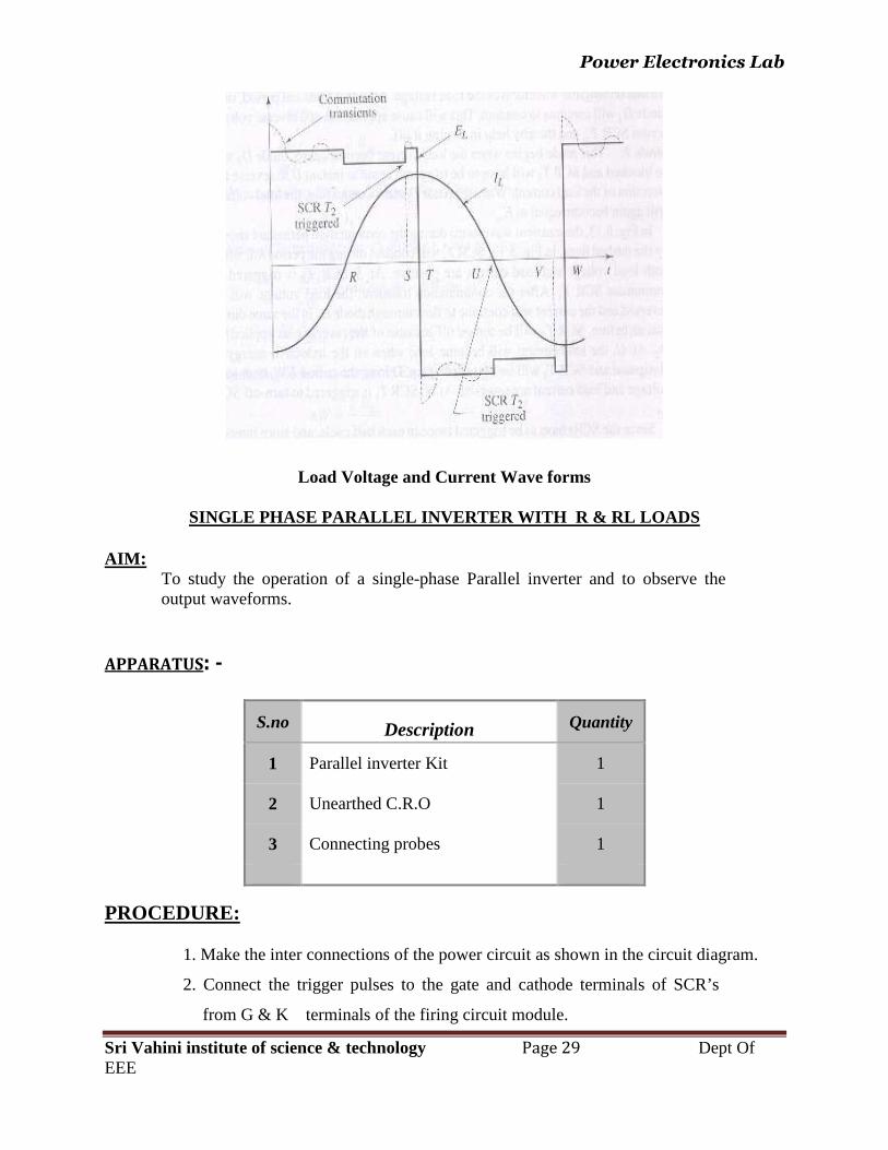
Load Voltage and Current Wave forms
SINGLE PHASE PARALLEL INVERTER WITH R & RL LOADS
AIM : To study the operation of a single-phase Parallel inverter and to observe the output waveforms.
APPARATUS: -
S.no Description Quantity
1 Parallel inverter Kit 1
2 Unearthed C.R.O 1
3 Connecting probes 1
PROCEDURE:
1. Make the inter connections of the power circuit as shown in the circuit diagram.
2. Connect the trigger pulses to the gate and cathode terminals of SCR’s
from G & K terminals of the firing circuit module.
Power Electronics Lab
Sri Vahini institute of science & technology Page 30 Dept Of EEE
3. Before switching ON the supply ensure that switching sequence is followed.
4. Connect CRO across the load.
1. Apply 10V DC input voltage by using 30V/2A RPS.
2. Switching on the toggle switch provided in the firing circuit module
triggers Thyristors.
3. Observe and plot the voltage across load, current waveforms with the help
of CRO.
4. Repeat step 7 by varying the firing angle in sequence of 30o.
5. Repeat step 7 and step 8 for RL loads.
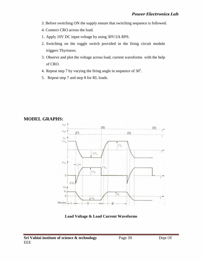
MODEL GRAPHS:
Load Voltage & Load Current Waveforms
Power Electronics Lab
Sri Vahini institute of science & technology Page 31 Dept Of EEE
Precautions: -
1. Identify the terminals of SCR carefully before connecting the circuit. 2. Use an unearthed CRO. 3. Before switching ON the supply see that the firing angle knob and the auto
transformer are in minimum position. 4. When the inverter frequency increases above the resonant frequency commutation
failure occurs. Switch OFF the DC supply and reduce the inverter frequency to continue the experiment.
RESULT: -
CIRCUIT DIAGRAM:
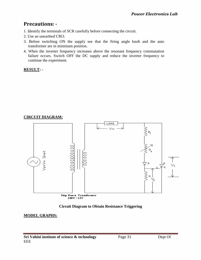
Circuit Diagram to Obtain Resistance Triggering
MODEL GRAPHS:
Power Electronics Lab
Sri Vahini institute of science & technology Page 32 Dept Of EEE
GATE FIRING CIRCUITS FOR SCR (R, RC, UJT) AIM : -
To trigger an SCR by using R, RC & UJT triggering circuits and observe the output waveforms for different firing angles.
APPARATUS: -
S.no Description Quantity
1 Triggering circuit Kit 1
2 Unearthed C.R.O 1
3 Connecting probes 1
PROCEDURE: Resistance Firing Circuit:
Power Electronics Lab
Sri Vahini institute of science & technology Page 33 Dept Of EEE
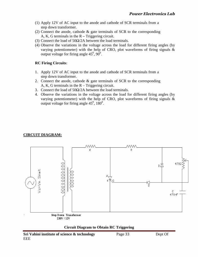
(1) Apply 12V of AC input to the anode and cathode of SCR terminals from a step down transformer.
(2) Connect the anode, cathode & gate terminals of SCR to the corresponding A, K, G terminals in the R – Triggering circuit.
(3) Connect the load of 50Ω/2A between the load terminals. (4) Observe the variations in the voltage across the load for different firing angles (by
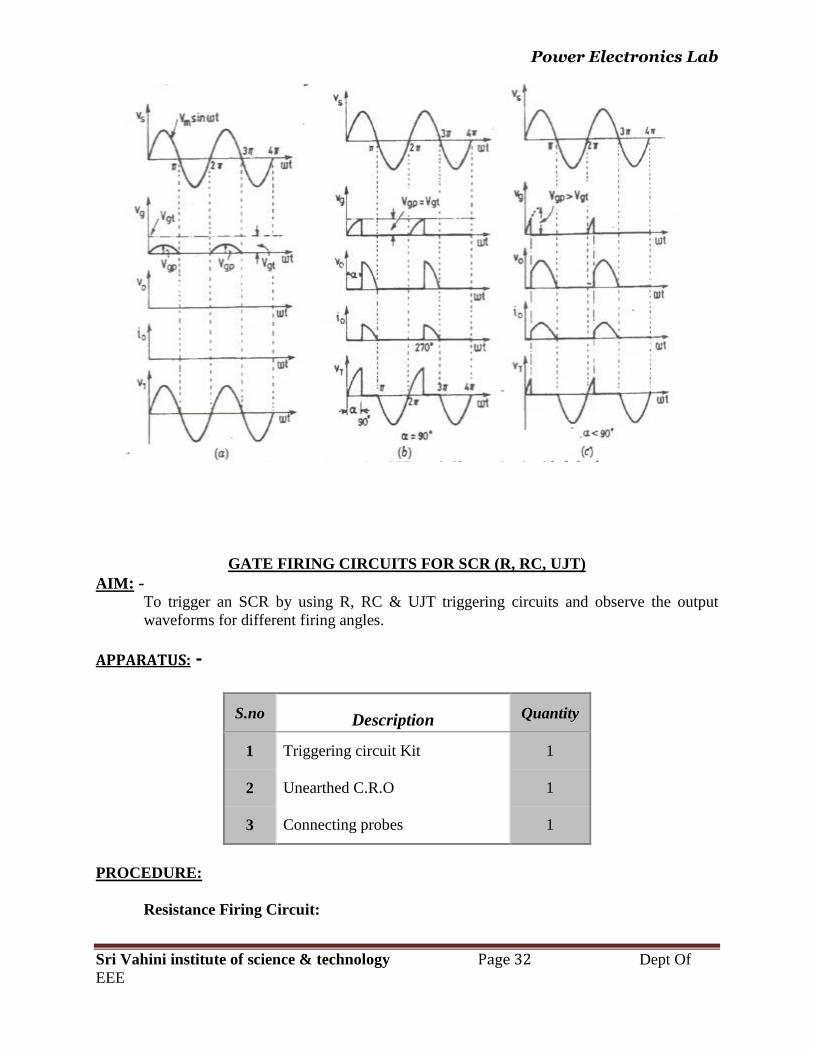
varying potentiometer) with the help of CRO, plot waveforms of firing signals & output voltage for firing angle 450, 900.
RC Firing Circuits : 1. Apply 12V of AC input to the anode and cathode of SCR terminals from a
step down transformer. 2. Connect the anode, cathode & gate terminals of SCR to the corresponding
A, K, G terminals in the R – Triggering circuit. 3. Connect the load of 50Ω/2A between the load terminals. 4. Observe the variations in the voltage across the load for different firing angles (by
varying potentiometer) with the help of CRO, plot waveforms of firing signals & output voltage for firing angle 450, 1800.
CIRCUIT DIAGRAM:
Circuit Diagram to Obtain RC Triggering
Power Electronics Lab
Sri Vahini institute of science & technology Page 34 Dept Of EEE
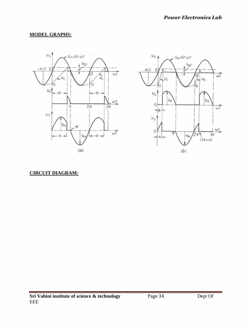
MODEL GRAPHS:
CIRCUIT DIAGRAM:
Power Electronics Lab
Sri Vahini institute of science & technology Page 35 Dept Of EEE
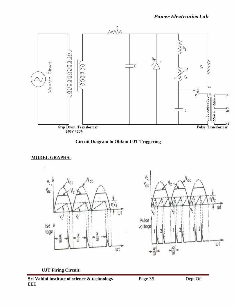
Circuit Diagram to Obtain UJT Triggering
MODEL GRAPHS:
UJT Firing Circuit:

Power Electronics Lab
Sri Vahini institute of science & technology Page 36 Dept Of EEE
1. Apply 12V of AC input to the anode and cathode of SCR terminals
from a step down transformer. 2. The rectified output is applied to the UJT terminals through the résistance
as shown in the circuit diagram. 3. Connect the cathode & gate terminals of SCR to the corresponding K, G
terminals in the UJT – Triggering circuit. 4. Connect the load of 50Ω/2A between the load terminals. 5. Switch ON the supply for UJT Triggering circuit. 6. Observe the variations in the voltage across the load for different firing angles (by
varying potentiometer) with the help of CRO, plot waveforms of firing signals & output voltage for firing angle 450, 1800.
PRECAUTIONS:
(1) Initially the potentiometer should be in minimum resistance position. (2) Vary the Potentiometer gradually. (3) Observe the output waveforms carefully on the CRO
RESULT:
Power Electronics Lab
Sri Vahini institute of science & technology Page 37 Dept Of EEE
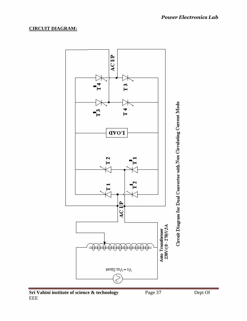
CIRCUIT DIAGRAM:
Power Electronics Lab
Sri Vahini institute of science & technology Page 38 Dept Of EEE
SINGLE PHASE DUAL CONVERTER WITH RL LOAD
AIM : To study the operation of a single phase dual converter in circulating and non – circulating current modes for various types of loads.
APPARATUS:
S.no Description Quantity
1 Dual Converter Kit 1
2 Unearthed C.R.O 1
3 Connecting probes 1
4 Loading resistor 50Ω/8A 1
5 Inductor with mid point 100 – 0 - mH
1
6 Inductor 25mH 1
PROCEDURE
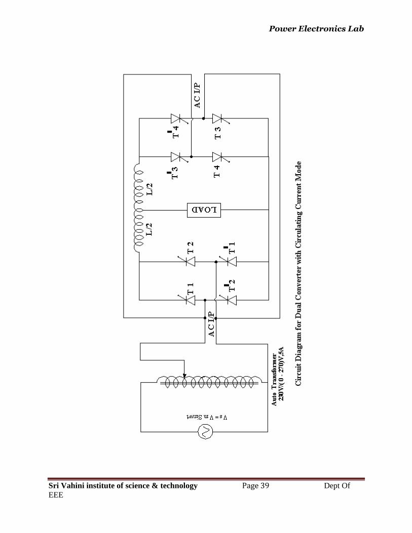
DUAL CONVERTER WITH NON - CIRCULATING CURRENT MODE (I) P – Converter is ON & N converter is OFF: 1) Make the connections as per the power circuit shown in the circuit diagram. 2) Connect the trigger pulses to the gate and cathode terminals of SCR’s
from G & K terminals of the firing circuit module. 3) Before switching on the supply ensure that switching sequence is
followed. 4) Connect CRO across the load. 5) Apply 10V AC input voltage using isolation transformer. 6) Make P – Converter ON & OFF the N Converter in the firing angle
circuit module. 7) Observe and plot the variation in the output voltage waveform across
the load terminals with the help of CRO. 8) Repeat step 7 by varying firing angle pulses in sequence.
Power Electronics Lab
Sri Vahini institute of science & technology Page 39 Dept Of EEE

Power Electronics Lab
Sri Vahini institute of science & technology Page 40 Dept Of EEE
(II) N – Converter is ON & P converter is OFF:
1) Make the connections as per the power circuit shown in the circuit diagram. 2) Connect the trigger pulses to the gate and cathode terminals of SCR’s
from G & K terminals of the firing circuit module. 3) Before switching on the supply ensure that switching sequence is
followed. 4) Connect CRO across the load. 5) Apply 10V AC input voltage using isolation transformer. 6) Make N – Converter ON & OFF the P Converter in the firing angle
circuit module. 7) Observe and plot the variation in the output voltage waveform across
the load terminals with the help of CRO. 8) Repeat step 7 by varying firing angle pulses in sequence.
DUAL CONVERTER WITH CIRCULATING CURRENT MODE 1) Make the connections as per the power circuit shown in the circuit diagram 2) Connect the trigger pulses to the gate and cathode terminals of SCR’s
from G & K terminals of the firing circuit module. 3) Before switching on the supply ensure that switching sequence is
followed. 4) Connect CRO across the load. 5) Apply 10V AC input voltage using isolation transformer. 6) Make N – Converter ON & OFF the P Converter in the firing angle
circuit module. 7) Observe and plot the variation in the output voltage waveform across
the load terminals with the help of CRO. 8) Repeat step 7 by varying firing angle pulses in sequence.
PRECAUTUIONS:
1. Identify the terminals of the SCR carefully before connecting the circuit. 2. Use an unearthed CRO. 3. Before switching ON the supply see that the firing angle knob and auto
transformer are in minimum position. 4. Without centre tapped inductor between the two converters don’t
operate in circulating current mode.
Power Electronics Lab
Sri Vahini institute of science & technology Page 41 Dept Of EEE
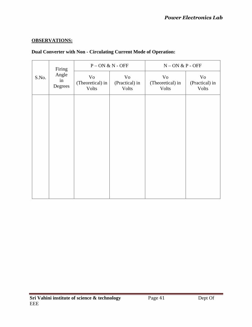
OBSERVATIONS: Dual Converter with Non - Circulating Current Mode of Operation:
S.No.
Firing Angle
in Degrees
P – ON & N - OFF N – ON & P - OFF
Vo (Theoretical) in
Volts
Vo (Practical) in
Volts
Vo (Theoretical) in
Volts
Vo (Practical) in
Volts

Power Electronics Lab
Sri Vahini institute of science & technology Page 42 Dept Of EEE
MODEL GRAPHS:
Power Electronics Lab
Sri Vahini institute of science & technology Page 43 Dept Of EEE
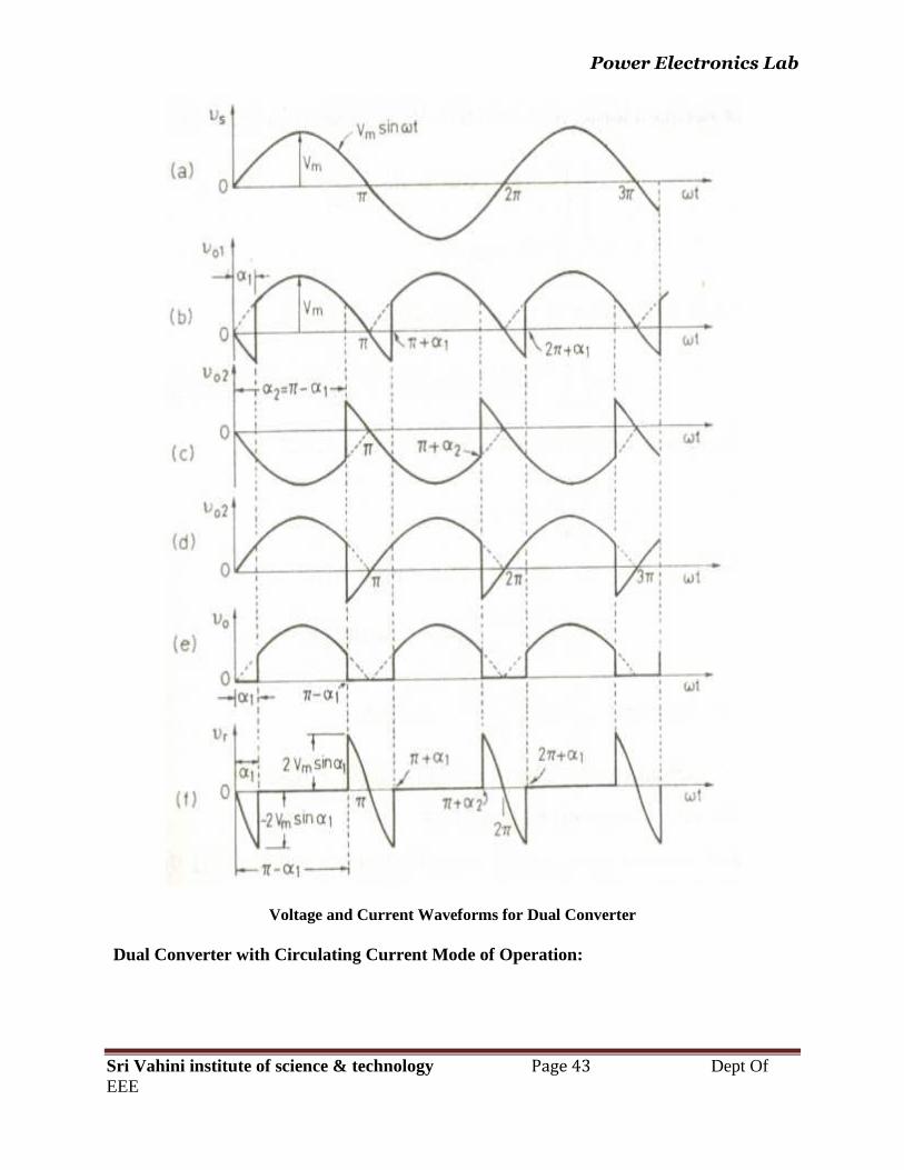
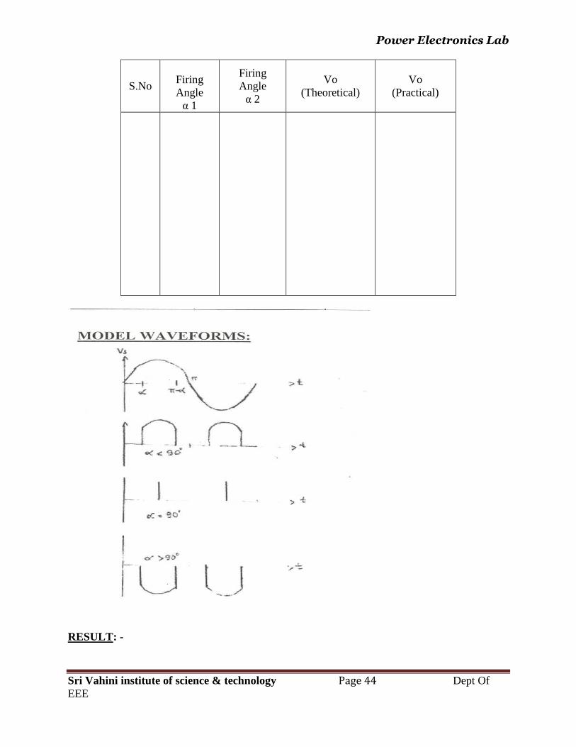
Voltage and Current Waveforms for Dual Converter Dual Converter with Circulating Current Mode of Operation:
Power Electronics Lab
Sri Vahini institute of science & technology Page 44 Dept Of EEE
S.No
Firing Angle α 1
Firing Angle α 2
Vo (Theoretical)
Vo (Practical)
RESULT: -

Power Electronics Lab
Sri Vahini institute of science & technology Page 45 Dept Of EEE


