
PJS-UM15M7 SYSTEM ON MODULE
Project Service S.a.s
PJS-UM15M7-STM32F7 v1.0 Datasheet
ST - STM32F746NG - based System-on-Module

2
PJS-UM15M7 SYSTEM ON MODULE
Project Service S.a.s
PJS-UM15M7-STM32 Datasheet © 2015 Project Service S.a.s. All Rights Reserved. No part of this document may be photocopied, reproduced, stored in a retrieval system, or transmitted, in any form or by any means whether, electronic, mechanical, or otherwise without the prior written permission of Project Service S.a.s. No warranty of accuracy is given concerning the contents of the information contained in this publication. To the extent permitted by law no liability (including liability to any person by reason of negligence) will be accepted by Project Service S.a.s, its subsidiaries or employees for any direct or indirect loss or damage caused by omissions from or inaccuracies in this document. Project Service S.a.s. reserves the right to change details in this publication without notice. Product and company names herein may be the trademarks of their respective owners.
Project Service S.a.s Via Paderno 31/C 24068, Seriate (BG) ITALY
Tel: +39-035-4520100 Fax: +39-035-4520731

3
PJS-UM15M7 SYSTEM ON MODULE
Document Revision History
Revision Date Notes 1.0 03/07/2015
Initial
4
PJS-UM15M7 SYSTEM ON MODULE
Document Revision History ............................................................................................................................... 3
1. Overview ...................................................................................................................................................... 5
1.1. General Information ......................................................................................................................... 5 1.2. Feature Summary ............................................................................................................................. 5 1.3. Block Diagram ................................................................................................................................... 6
2. Main Hardware Components ...................................................................................................................... 7
2.1. ST Microelectronic STM32F746.......................................................................................................7 2.2. Memory ............................................................................................................................................8 2.3. 10/100 Ethernet PHY…….................................................................................................................. 8 2.4. EUI-48™ Node Identity….................................................................................................................. 8
3. External Connectors.................................................................................................................................... 9
3.1. PJS-UM15M7-STM32 SOM Connector Pin-out ............................................................................... 10 3.2. 80 Pin connector pin Mux .............................................................................................................. 15 3.3. Unavailable Signals of STM32F7..................................................................................................... 17
4. SOM's interfaces ........................................................................................................................................ 18
4.1. Display Interface .............................................................................................................................18 4.2. Megabit Ethernet............................................................................................................................18 4.3. USB 2.0 F.S …................................................................................................................................... 19 4.4. USB 2.0 H.S .................................................................................................................................... 19 4.5. MMC/SD/SDIO ................................................................................................................................ 20 4.6. SPI................................................................................................................................................... 20 4.7. I2C………………...................................................................................................................……………… 20 4.8. JTAG/ETM…….................................................................................................................................. 21 4.9. BOOT............................................................................................................................................... 21 4.10. General Purpose IOs ..................................................................................................................... 21
5. Absolute Maximum Characteristics .......................................................................................................... 22
6. Operational Characteristics ...................................................................................................................... 22
6.1. Power supplies .............................................................................................................................. 22
7. Mechanical Drawings ................................................................................................................................ 23
8. Contact Information .................................................................................................................................. 24
5
PJS-UM15M7 SYSTEM ON MODULE
1. Overview
1.1. General Information
This document describes the hardware architecture of the PJS-UM15M7-STM32 SOM. The PJS-UM15M7-STM32 is a high performance System-on-Module and is intended to provide a flexible platform for embedded application that require an ideal building block that easily integrates powerful graphics, rich connectivity and as well as high-processing power. The PJS-UM15M7-STM32 is based on the ST Microelectronic STM32F746 versatile, low-power, high-integration microcontroller.
1.2. Feature Summary
• ST Microelectronic STM32F746 (Single ARM® Cortex™-M7 Core, up to 200 MHz)
• 32 MB SDRAM
• 64 MB QSPI NOR Flash for storage memory
• Real-Time Clock (RTC)
• 24bit LCD-TTL interface up to XGA resolution
• On-board 10/100 Mbps Ethernet PHY
• On-board 2K bits I2C™ Serial EEPROM with EUI-48™ Node Identity
• 1 x USB 2.0 full-speed, device/host/OTG controller with on-chip PHY
• 1 x USB 2.0 high-speed in full-speed, device/host/OTG controller with dedicated DMA, on-
chip full-speed PHY
• 1 x SD/SDIO/MMC card host interface
• Serial interfaces (SPI, I2C, UART)
• CAN Bus
• External Interface using two 80-pin 0.5mm pitch connectors
• Single 3.3V power supply
• 40mm x 40mm compact module
• Mounting holes reducing the risk of connector-to-PCB intermittence
• Compliant with the Restriction of Hazardous Substances (RoHS) directive

6
PJS-UM15M7 SYSTEM ON MODULE
1.3. Block Diagram
7
PJS-UM15M7 SYSTEM ON MODULE
2. Main Hardware Components
This section summarizes the main hardware building blocks of the PJS-UM15M7-STM32 SOM
2.1. ST Microelectronic STM32F746
The STM32F746 device is based on the high-performance ARM® Cortex®-M7 32-bit RISC core operating at up to 216 MHz frequency.
The Cortex®-M7 core features a single floating point unit (SFPU) precision which supports all ARM® single-precision dataprocessing instructions and data types. It also implements a full set of DSP instructions and a memory protection unit (MPU) which enhances application security.
It also feature standard and advanced communication interfaces.
• Up to four I2Cs
• Six SPIs, three I2Ss in duplex mode.
• Four USARTs plus four UARTs
• An USB OTG full-speed and a USB OTG high-speed with full-speed capability (with the ULPI),
• Two CANs
• Two SAI serial audio interfaces
• An SDMMC host interface
• Ethernet and camera interface
• 24-bit parallel digital RGB LCD-TFT display controller up to XGA resolution
• Chrom-ART Accelerator™.
• SPDIF-Rx interface
• HDMI-CEC
8
PJS-UM15M7 SYSTEM ON MODULE
2.2. Memory
2.2.1. S D R A M
The PJS-UM15M7-STM32 SOM is available with 32MB of 166Mhz 32-bit SDRAM memory using the ISSI IS42S32800G-6BLI. The SDRAM memory resides at chip select FMC_SDNE0 of the integrated Flexible Memory Controller (FMC) of the STM32F7 MCU. The STM32F7 Flexible Memory controller operates the SDRAM with the SDRAM clock of 100 MHz (HCLK/2), Burst length = 8 and CL2.
2.2.2. Non-volatile Storage Memory Th The PJS-UM15M7-STM32 provides 64 MBytes QSPI NOR Flash memory, using the Micron MT25QL512ABA8E12-0SIT device. The MT25Q is a high-performance multiple input/output serial Flash memory device manufactured on 45nm NOR technology. It features a high-speed SPI-compatible bus interface, execute-in-place (XIP) functionality, advanced write protection mechanisms, and extended address access. Innovative, high-performance, dual and quad input/ output commands enable double or quadruple the transfer bandwidth for READ and PROGRAM operations.
2.3. 10/100 Ethernet PHY
The PJS-UM15M7-STM32 features the KSZ8081RNAIA, a robust fully featured 10/100 single port Physical Layer device offering low power consumption, including several intelligent power down states. The KSZ8081RNAIA is a completely integrated double speed (10Base-T/100Base-T) Ethernet Physical Layer Transceiver for transmission and reception of data over standard CAT-5 unshielded twisted pair (UTP) cable. The KSZ8081RNAIA provides the Reduced Media Independent Interface (RMII) for direct connection to RMII-compliant MACs in Ethernet processors. The STM32F7 SOM provides a 25 MHz quartz crystal as a clock reference to the Ethernet PHY device. The KSZ8081RNAIA PHY device drives the 50 MHz RMII reference clock input of the integrated Ethernet controller of the STM32F7 MCU. When not accessed, the PHY can be switched to the Power-Down mode under the software control.
2.4. EUI-48™ Node Identity
The PJS-UM15M7-STM32 contains the Microchip 24AA025E48 a 2 Kbit Electrically Erasable PROM. The device is organized as two blocks of 128 x 8-bit memory with a 2-wire serial interface. The 24AA025E48 is programmed at the factory with a globally unique, EUI-48™ and EUI-64™ compatible node address stored in the upper half of the array and permanently write-protected. The remaining 1,024 bits are available for application use.

9
PJS-UM15M7 SYSTEM ON MODULE
3. External Connectors
The PJS-UM15M7-STM32 SOM exposes two 80 pin 0.5mm pitch connectors. The recommended mating connector for baseboard interfacing are:
1. FCI - 61082-081402LF
In addition to the two 80 pin interface PJS-UM14-STM32 SOM exposes a 10-pin , 1.27mm pitch, box header (For JTAG & SWJ-DP).
Pin#: Pin number on the FCI connector
Pin Name: Default PJS-UM15M7 SOM pin name
Type: Pin type & direction:
I – In
O – Out
DS – Differential Signal
A – Analog
Power – Power Pin
Pin Group: Pin functionality group
STM32F746 Ball: Ball number
CN2 CN3

10
PJS-UM15M7 SYSTEM ON MODULE
3.1. PJS-UM15M7_STM32 SOM Connectors Pin-out 3.1.1. CN2 Connector:
Pin # Pin Name Type Pin Group GPIO STM32F746 Ball
1 PE6 IO General purpose PE[06] B2
2 GND POWER Digital GND
3 GND POWER Digital GND
4 JTAG_TMS IO System debug JTMS-SWDIO pin PA[13] A15
5 PE5 IO General purpose PE[05] B1
6 JTAG_TCK IO System debug JTCK-SWCLK pin PA[14] A14
7 GND POWER Digital GND
8 RST I System debug Reset pin NRST J1
9 PE4 IO General purpose PE[04] A1
10 JTAG_TDI IO System debug JTDI pin PA[15] A13
11 GND POWER Digital GND
12 JTAG_TRST IO System debug TRST pin PB[04] A9
13 PE3 IO General purpose PE[03] A2
14 JTAG_TDO IO System debug JTDO-SWO pin PB[03] A10
15 GND POWER Digital GND
16 GND POWER Digital GND
17 PE2 IO General purpose PE[02] A3
18 PD3 IO General purpose PD[03] C11
19 GND POWER Digital GND
20 PD4 IO General purpose PD[04] D11
21 PD5 IO General purpose PD[05] C10
22 GND POWER Digital GND
23 PD6 IO General purpose PD[06] B11
24 SDIO_CK O SDMMC Interface - Clock PC[12] A12
25 PD7 IO General purpose PD[07] A11
26 SDIO_CMD IO SDMMC Interface - Command PD[02] D12
27 GND POWER Digital GND
28 SDIO_D3 IO SDMMC Interface - DATA3 PC[11] B13
29 ETH_LINK/ACT O Ethernet Link/Act LED
30
SDIO_D2 IO SD Interface - DATA2 PC[10] B14
31 GND POWER Digital GND
32 SDIO_D1 IO SD Interface - DATA1 PC[09] F14
33 ETH_TX_P DS Ethernet PHY positive transmit signal
34 SDIO_D0 IO SD Interface - DATA0 PC[08] G14
35 ETH_TX_N DS Ethernet PHY negative transmit signal
11
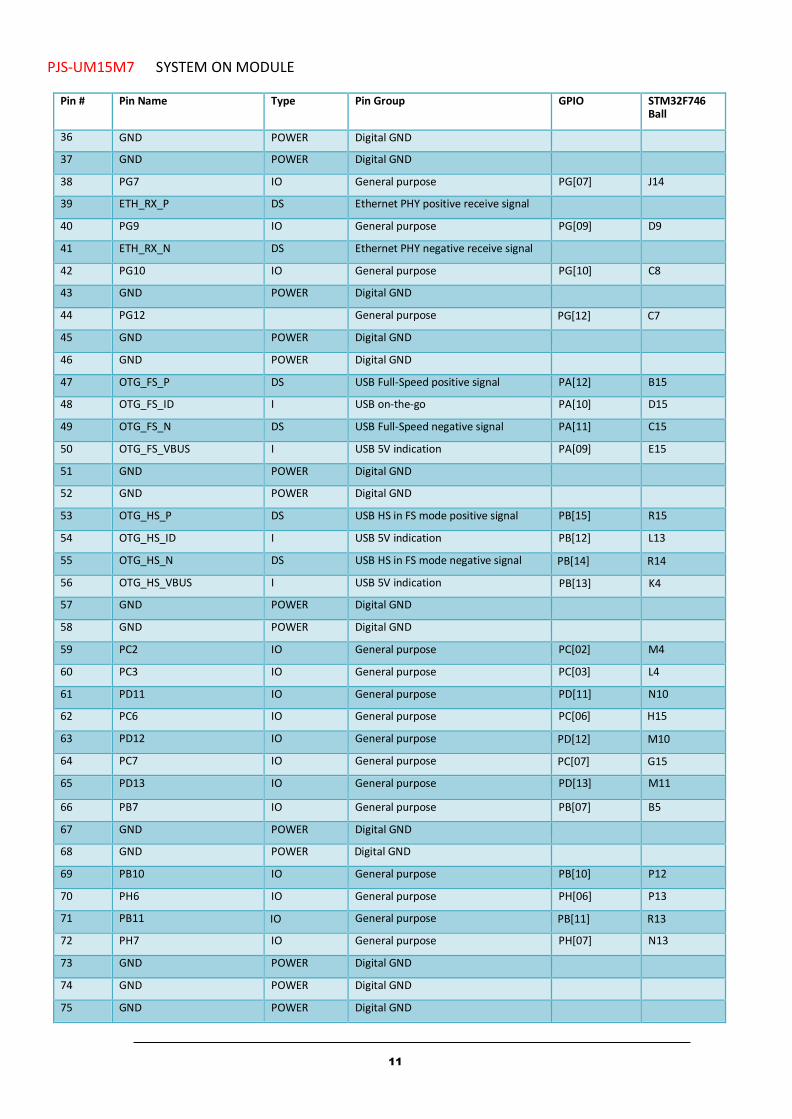
PJS-UM15M7 SYSTEM ON MODULE
Pin # Pin Name Type Pin Group GPIO STM32F746 Ball
36 GND POWER Digital GND
37 GND POWER Digital GND
38 PG7 IO General purpose PG[07] J14
39 ETH_RX_P DS Ethernet PHY positive receive signal
40 PG9 IO General purpose PG[09] D9
41 ETH_RX_N DS Ethernet PHY negative receive signal
42 PG10 IO General purpose PG[10] C8
43 GND POWER Digital GND
44 PG12 General purpose PG[12] C7
45 GND POWER Digital GND
46 GND POWER Digital GND
47 OTG_FS_P DS USB Full-Speed positive signal PA[12] B15
48 OTG_FS_ID I USB on-the-go PA[10] D15
49 OTG_FS_N DS USB Full-Speed negative signal PA[11] C15
50 OTG_FS_VBUS I USB 5V indication PA[09] E15
51 GND POWER Digital GND
52 GND POWER Digital GND
53 OTG_HS_P DS USB HS in FS mode positive signal PB[15] R15
54 OTG_HS_ID I USB 5V indication PB[12] L13
55 OTG_HS_N DS USB HS in FS mode negative signal PB[14] R14
56 OTG_HS_VBUS I USB 5V indication PB[13] K4
57 GND POWER Digital GND
58 GND POWER Digital GND
59 PC2 IO General purpose PC[02] M4
60 PC3 IO General purpose PC[03] L4
61 PD11 IO General purpose PD[11] N10
62 PC6 IO General purpose PC[06] H15
63 PD12 IO General purpose PD[12] M10
64 PC7 IO General purpose PC[07] G15
65 PD13 IO General purpose PD[13] M11
66 PB7 IO General purpose PB[07] B5
67 GND POWER Digital GND
68 GND POWER Digital GND
69 PB10 IO General purpose PB[10] P12
70 PH6 IO General purpose PH[06] P13
71 PB11 IO General purpose PB[11] R13
72 PH7 IO General purpose PH[07] N13
73 GND POWER Digital GND
74 GND POWER Digital GND
75 GND POWER Digital GND

12
PJS-UM15M7 SYSTEM ON MODULE
76 GND POWER Digital GND
77 3V3 POWER 3.3 V power supply IN
78 3V3 POWER 3.3 V power supply IN
79 3V3 POWER 3.3 V power supply IN
80 3V3 POWER 3.3 V power supply IN

13
PJS-UM15M7 SYSTEM ON MODULE
3.1.2. CN3 Connector:
Pin # Pin Name Type Pin Group GPIO STM32F746 Ball
1 3V3 POWER 3.3 V power supply IN
2 3V3 POWER 3.3 V power supply IN
3 3V3 POWER 3.3 V power supply IN
4 3V3 POWER 3.3 V power supply IN
5 GND POWER Digital GND
6 GND POWER Digital GND
7 GND POWER Digital GND
8 GND POWER Digital GND
9 BOOT0 I BOOT selection pin
10 VBAT_IN POWER RTC backup battery IN
C1
11 nRST I System RESET pin
12 NC Leave not connected
13 I2C1_SCL IO I2C interface PB[08] A7
14 I2C2_SCL IO I2C interface[1] H4
15 I2C1_SDA IO I2C interface PB[09] B4
16 I2C2_SDA IO I2C interface[1] H5
17 GND POWER Digital GND
18 GND POWER Digital GND
19 LCD_B0 O LCD-TTL Interface B0 B10
20 LCD_B4 O LCD-TTL Interface B4 D8
21 LCD_B1 O LCD-TTL Interface B1 B9
22 LCD_B5 O LCD-TTL Interface B5 D7
23 LCD_B2 O LCD-TTL Interface B2 C9
24 LCD_B6 O LCD-TTL Interface B6 C6
25 LCD_B3 O LCD-TTL Interface B3 D10
26 LCD_B7 O LCD-TTL Interface B7 C5
27 GND POWER Digital GND
28 GND POWER Digital GND
29 LCD_G0 O LCD-TTL Interface G0 J12
30
LCD_G4 O LCD-TTL Interface G4 G12
31 LCD_G1 O LCD-TTL Interface G1 H12
32 LCD_G5 O LCD-TTL Interface G5 G13
33 LCD_G2 O LCD-TTL Interface G2 J13
34 LCD_G6 O LCD-TTL Interface G6 F12
35 LCD_G3 O LCD-TTL Interface G3 H13
Pin # Pin Name Type Pin Group GPIO STM32F746 Ball
36 LCD_G7 O LCD-TTL Interface G7 F13
14
PJS-UM15M7 SYSTEM ON MODULE
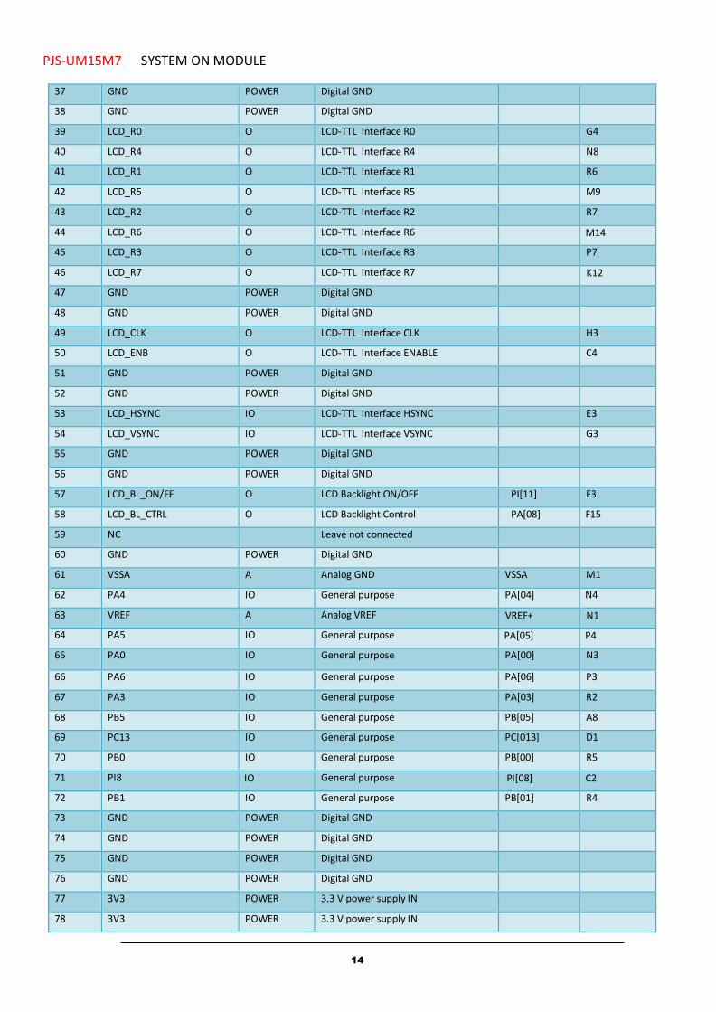
37 GND POWER Digital GND
38 GND POWER Digital GND
39 LCD_R0 O LCD-TTL Interface R0 G4
40 LCD_R4 O LCD-TTL Interface R4 N8
41 LCD_R1 O LCD-TTL Interface R1 R6
42 LCD_R5 O LCD-TTL Interface R5 M9
43 LCD_R2 O LCD-TTL Interface R2 R7
44 LCD_R6 O LCD-TTL Interface R6 M14
45 LCD_R3 O LCD-TTL Interface R3 P7
46 LCD_R7 O LCD-TTL Interface R7 K12
47 GND POWER Digital GND
48 GND POWER Digital GND
49 LCD_CLK O LCD-TTL Interface CLK H3
50 LCD_ENB O LCD-TTL Interface ENABLE
C4
51 GND POWER Digital GND
52 GND POWER Digital GND
53 LCD_HSYNC IO LCD-TTL Interface HSYNC
E3
54 LCD_VSYNC IO LCD-TTL Interface VSYNC
G3
55 GND POWER Digital GND
56 GND POWER Digital GND
57 LCD_BL_ON/FF O LCD Backlight ON/OFF PI[11] F3
58 LCD_BL_CTRL O LCD Backlight Control
PA[08] F15
59 NC Leave not connected
60 GND POWER Digital GND
61 VSSA A Analog GND VSSA M1
62 PA4 IO General purpose PA[04] N4
63 VREF A Analog VREF VREF+ N1
64 PA5 IO General purpose PA[05] P4
65 PA0 IO General purpose PA[00] N3
66 PA6 IO General purpose PA[06] P3
67 PA3 IO General purpose PA[03] R2
68 PB5 IO General purpose PB[05] A8
69 PC13 IO General purpose PC[013] D1
70 PB0 IO General purpose PB[00] R5
71 PI8 IO General purpose PI[08] C2
72 PB1 IO General purpose PB[01] R4
73 GND POWER Digital GND
74 GND POWER Digital GND
75 GND POWER Digital GND
76 GND POWER Digital GND
77 3V3 POWER 3.3 V power supply IN
78 3V3 POWER 3.3 V power supply IN

15
PJS-UM15M7 SYSTEM ON MODULE
79 3V3 POWER 3.3 V power supply IN
80 3V3 POWER 3.3 V power supply IN
Notes: [1] I2C2 Interface is used on-som. Pin mode can’t be changed.
3.2. 80 pin Connector Pin Mux
The table below summarizes the additional available functionality for each pin- of two 80 pin FCI connector.
3.2.1. CN2 Connector Pin Mux:
PIN GPIO MODE 0 MODE 1 MODE 2 MODE 3 MODE 4 MODE 5 MODE 6
1 PE[06] TRACED3
TIM1_BKIN2 TIM9_CH2 SPI4_MOSI SAI1_SD_A SAI2_MCK_B
5 PE[05] TRACED2
TIM9_CH1 SPI4_MISO SAI1_SCK_A
9 PE[04] TRACED1
SPI4_NSS SAI1_FS_A
13 PE[03] TRACED0
SAI1_SD_B
17 PE[02] TRACECLK SPI4_SCK SAI1_MCLK_A
18 PD[03] SPI2_SCK I2S2_CK USART2_CTS
20 PD[04] USART2_RTS
21 PD[05] USART2_TX
23 PD[06] SPI3_MOSI
I2S3_SD SAI1_SA_A USART2_RX
24 PC[12] TRACED3
SPI3_MOSI I2S3_SD USART3_CK UART5_TX
25 PD[07] USART2_CK
SPDIFRX_IN0
26 PD[02] TRACED2
TIM3_ETR UART5_RX
28 PC[11] SPI3_MISO
USART3_RX UART4_RX
30 PC[10] SPI3_SCK
I2S3_CK USART3_TX UART4_TX
32 PC[09] MCO2
TIM3_CH4 TIM8_CH4 I2C3_SDA I2S_CKIN UART5_CTS
34 PC[08] TRACED1
TIM3_CH3 TIM8_CH3 UART5_RTS USART6_CK
38 PG[07] USART6_CK
40 PG[09] SPDIFRX_IN3
USART6_RX SAI2_FS_B
42 PG[10] SAI2_SD_B
44 PG[12] LPTIM1_IN1
SPI6_MISO SPDIFRX_IN1 USART6_RTS
47 PA[12] TIM1_ETR
USART1_RTS SAI2_FS_B CAN1_TX
48 PA[10] TIM1_CH3
USART1_RX
49 PA[11] TIM1_CH4
USART1_CTS CAN1_RX

16
PJS-UM15M7 SYSTEM ON MODULE
50 PA[09] TIM1_CH2
I2C3_SMBA SPI2_SCK I2S2__CK USART1_TX
53 PB[15] RTC_REFIN
TIM1_CH3N TIM8_CH3N SPI2_MOSI I2S2_SD TIM12_CH2
54 PB[12] TIM1_BKIN
I2C2_SMBA SPI2_NSS I2S2_WS USART3_CK CAN2_RX
55 PB[14] TIM1_CH2N
TIM8_CH2N SPI2_MISO USART3_RTS TIM12_CH1
56 PB[13] TIM1_CH1N
SPI2_SCK I2S2_CK USART3_CTS CAN2_TX
59 PC[02] SPI2_MISO
60 PC[03] SPI2_MOSI
I2S2_SD ADC123_IN13
61 PD[11] I2C4_SMBA
USART3_CTS SAI2_SD_A
62 PC[06] TIM3_CH1
TIM8_CH1 I2S2_MCK USART6_TX
63 PD[12] TIM4_CH1
LPTIM1_IN1 I2C4_SCL USART3_RTS SAI1_FS_A
64 PC[07] TIM3_CH2
TIM8_CH2 I2S3_MCK USART6_RX
65 PD[13] TIM4_CH1
LPTIM1_OUT I2C4_SDA SAI2_SCK_A
66 PB[07] TIM4_CH2
I2C1_SDA USART1_RX
69 PB[10] TIM2_CH3
I2C2_SCL SPI2_SCK I2S2_CK USART3_TX
70 PH[06] TIM3_CH2
TIM8_CH2 I2S3_MCK USART6_RX
71 PB[11] TIM2_CH4
I2C2_SDA USART3_RX
72 PH[07] I2C3_SCL
SPI5_MISO
3.2.2. CN3 Connector Pin Mux:
PIN GPIO MODE 0 MODE 1 MODE 2 MODE 3 MODE 4 MODE 5 MODE 6
9 PB[08] TIM4_CH3
TIM10_CH1 I2C1_SCL CAN1_RX SDIO_D4 DCMI_D6
11 PB[09] TIM4_CH4
TIM11_CH1 I2C1_SDA SPI2_NSS I2S2_WS CAN1_TX SDIO_D5
62 PA[04] SP1_NSS
I2S1_WS SPI3_NSS I2S3_WS USART2_CK ADC12_IN4 DAC_OUT1
64 PA[05] TIM2_CH1
TIM2_ETR TIM8_CH1N SPI1_SCK I2S1_CK ADC12_IN5 DAC_OUT2
65 PA[00] TIM2_CH1
TIM2_ETR
TIM5_CH1 TIM8_ETR USART2_CTS UART4_TX SAI2_SD_B ADC123_IN0
WKUP0
66 PA[06] TIM1_BKIN TIM3_CH1 TIM8_BKIN SPI1_MISO TIM13_CH1 ADC12_IN6
67 PA[03] TIM2_CH4
TIM5_CH4 TIM9_CH2 USART2_RX ADC123_IN3
68 PB[05] TIM3_CH2
I2C1_SMBA SPI1_MOSI I2S1_SD SPI3_MOSI I2S3_SD CAN2_RX
69 PC[13] RTC_TAMP1
RTC_TS RTC_OUT WKUP2
70 PB[00] TIM1_CH2N
TIM3_CH3 TIM8_CH2N UART4_CTS ADC12_IN8
71 PI[08] RTC_TAMP2
RTC_TS WKUP3
72 PB[01] TIM3_CH3N
TIM3_CH4 TIM8_CH3N ADC12_IN9
17
PJS-UM15M7 SYSTEM ON MODULE
3.3. Unavailable Signals of STM32F7
The memory interface and also the QSPI signals are not available on the interface connectors.
18
PJS-UM15M7 SYSTEM ON MODULE
4. SOM's interfaces
4.1. Display Interface
The PJS-UM15M7-STM32 SOM provides a 24-bit parallel digital RGB (Red, Green, Blue) and delivers all signals to interface directly to a broad range of LCD and TFT panels up to XGA (1024x768) resolution with the following features:
• 2 displays layers with dedicated FIFO (64x32-bit)
• Color Look-Up table (CLUT) up to 256 colors (256x24-bit) per layer
• Up to 8 Input color formats selectable per layer
• Flexible blending between two layers using alpha value (per pixel or constant)
• Flexible programmable parameters for each layer
• Color keying (transparency color)
• Up to 4 programmable interrupt events.
4.2. Megabit Ethernet
Megabit Ethernet Features:
The Ethernet Media Access Controller (MAC) is designed to support 10/100 Mbps Ethernet/IEEE 802.3 networks. An external Megabit magnetics is required to complete the interface to the media.
Megabit Ethernet Signals (CN2):
Signal Pin # Type Description
ETH_TX_P 33 DS Positive transmit signal ETH_TX_N 35 DS Negative transmit signal ETH_RX_P 39 DS Positive receive signal ETH_RX_N 41 DS Negative receive signal ETH_LINK/ACT 29 O Ethernet Link/Act LED
19
PJS-UM15M7 SYSTEM ON MODULE
Signal Pin # Type Description
OTG_FS_P 47 DS Positive USB F.S data
OTG_FS_N 49 DS Negative USB F.S data
OTG_FS_VBUS 50
I USB 2.0 VBUS indicator (5V)
OTG_FS_ID 48 I USB OTG
Signal Pin # Type Description
OTG_HS_P 53 DS Positive USB F.S data
OTG_HS_N 55 DS Negative USB F.S data
OTG_HS_VBUS 56 I USB 2.0 VBUS indicator (5V)
OTG_HS_ID 54 I USB OTG
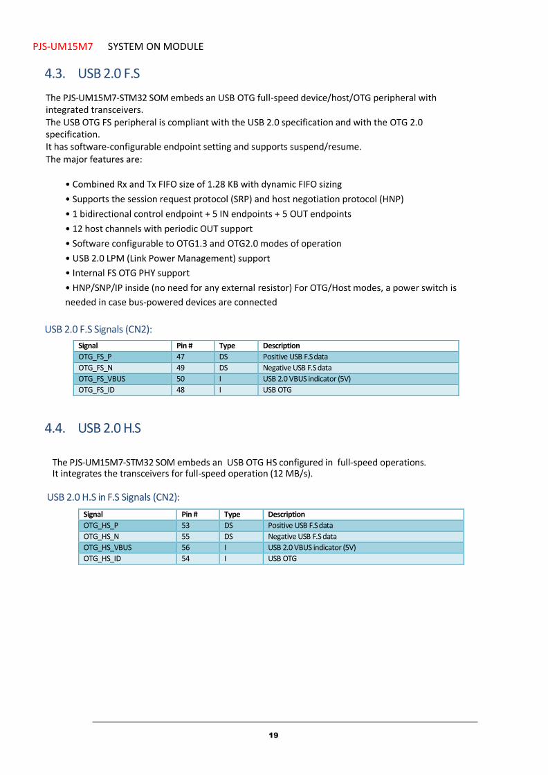
4.3. USB 2.0 F.S
The PJS-UM15M7-STM32 SOM embeds an USB OTG full-speed device/host/OTG peripheral with integrated transceivers. The USB OTG FS peripheral is compliant with the USB 2.0 specification and with the OTG 2.0 specification. It has software-configurable endpoint setting and supports suspend/resume. The major features are:
• Combined Rx and Tx FIFO size of 1.28 KB with dynamic FIFO sizing
• Supports the session request protocol (SRP) and host negotiation protocol (HNP)
• 1 bidirectional control endpoint + 5 IN endpoints + 5 OUT endpoints
• 12 host channels with periodic OUT support
• Software configurable to OTG1.3 and OTG2.0 modes of operation
• USB 2.0 LPM (Link Power Management) support
• Internal FS OTG PHY support
• HNP/SNP/IP inside (no need for any external resistor) For OTG/Host modes, a power switch is
needed in case bus-powered devices are connected
USB 2.0 F.S Signals (CN2):
4.4. USB 2.0 H.S
The PJS-UM15M7-STM32 SOM embeds an USB OTG HS configured in full-speed operations. It integrates the transceivers for full-speed operation (12 MB/s).
USB 2.0 H.S in F.S Signals (CN2):

20
PJS-UM15M7 SYSTEM ON MODULE
Signal Pin # Type Description
I2C1_SCL 13 IO I2C1 I2C clock, open drain
I2C1_SDA 15 IO I2C1 I2C data, open drain
Signal Pin # Type Description
I2C2_SCL 14 IO I2C2 I2C clock, open drain
I2C2_SDA 16 IO I2C2 I2C data, open drain
4.5. MMC/SD/SDIO
The PJS-UM15M7-STM32 SOM supports MultiMediaCard System Specification Version 4.2 in two different databus modes: 1-bit, 4-bit(default).
SDIO Signals (CN2):
4.6. SPI
The PJS-UM15M7-STM32 SOM feature up to four SPIs in slave and master modes in full-duplex and simplex communication modes. SPI1, SPI4 can communicate at up to 50 Mbits/s, SPI2 and SPI3 can communicate at up to 25 Mbit/s. The 3-bit prescaler gives 8 master mode frequencies and the frame is configurable from 4 to 16 bits. The SPI interfaces support NSS pulse mode, TI mode and Hardware CRC calculation. All SPIs can be served by the DMA controller.
4.7. I2C
I2C-1, 2 Interface connectivity peripherals provide serial interface for external devices. Data rates of up to
400 kbps are supported.
I2C1 Signals (CN3):
I2C2 Signals (CN3):
Note: I2C2 interface is used by E2P on-som devices. Pin configuration for I2C2 signal can’t be changed.
Signal Pin # Type Description
SDIO_CLK 24 O Clock for MMC/SD/SDIO card
SDIO_CMD 26 IO CMD line connect to card
SDIO_DATA0 34 IO DAT0 line in all modes (also used to detect busy state)
SDIO_DATA1 32 IO DAT1 line-in
SDIO_DATA2 30 IO DAT2 line
SDIO_DATA3 28 IO DAT3 line-in
21
PJS-UM15M7 SYSTEM ON MODULE
Signal Pin # Type Description
JTAG_TDI 10 I JTAG data-in
JTAG_TRST 12 I JTAG reset
JTAG_TMS 4 I JTAG test mode select
JTAG_TCK 6 O JTAG test clock
JTAG_TDO 14 O JTAG data-out
Signal Pin # Type Description
ETM_TRACED3 1 IO TRACEDATA[3] TRACEDATA[3] TRACEDATA[3]
ETM_TRACED2 5 IO TRACEDATA[2] ETM_TRACED1 9 IO TRACEDATA[1] ETM_TRACED0 13 IO TRACEDATA[0] ETM_TRACECLK 17 IO TRACECLOCK
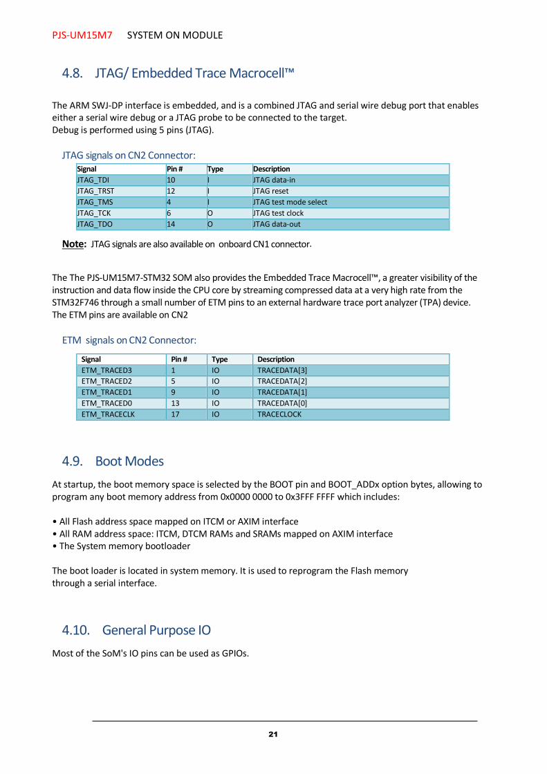
4.8. JTAG/ Embedded Trace Macrocell™
The ARM SWJ-DP interface is embedded, and is a combined JTAG and serial wire debug port that enables either a serial wire debug or a JTAG probe to be connected to the target. Debug is performed using 5 pins (JTAG).
JTAG signals on CN2 Connector:
Note: JTAG signals are also available on onboard CN1 connector.
The The PJS-UM15M7-STM32 SOM also provides the Embedded Trace Macrocell™, a greater visibility of the instruction and data flow inside the CPU core by streaming compressed data at a very high rate from the STM32F746 through a small number of ETM pins to an external hardware trace port analyzer (TPA) device. The ETM pins are available on CN2
ETM signals on CN2 Connector:
4.9. Boot Modes
At startup, the boot memory space is selected by the BOOT pin and BOOT_ADDx option bytes, allowing to program any boot memory address from 0x0000 0000 to 0x3FFF FFFF which includes: • All Flash address space mapped on ITCM or AXIM interface • All RAM address space: ITCM, DTCM RAMs and SRAMs mapped on AXIM interface • The System memory bootloader The boot loader is located in system memory. It is used to reprogram the Flash memory through a serial interface.
4.10. General Purpose IO
Most of the SoM's IO pins can be used as GPIOs.
22
PJS-UM15M7 SYSTEM ON MODULE
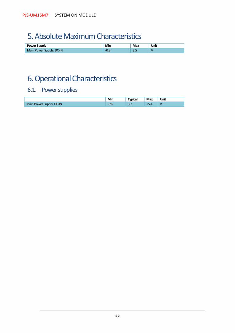
5. Absolute Maximum Characteristics
Power Supply Min Max Unit
Main Power Supply, DC-IN -0.3 3.5 V
6. Operational Characteristics
6.1. Power supplies
Min Typical Max Unit
Main Power Supply, DC-IN -5% 3.3 +5% V
23
PJS-UM15M7 SYSTEM ON MODULE
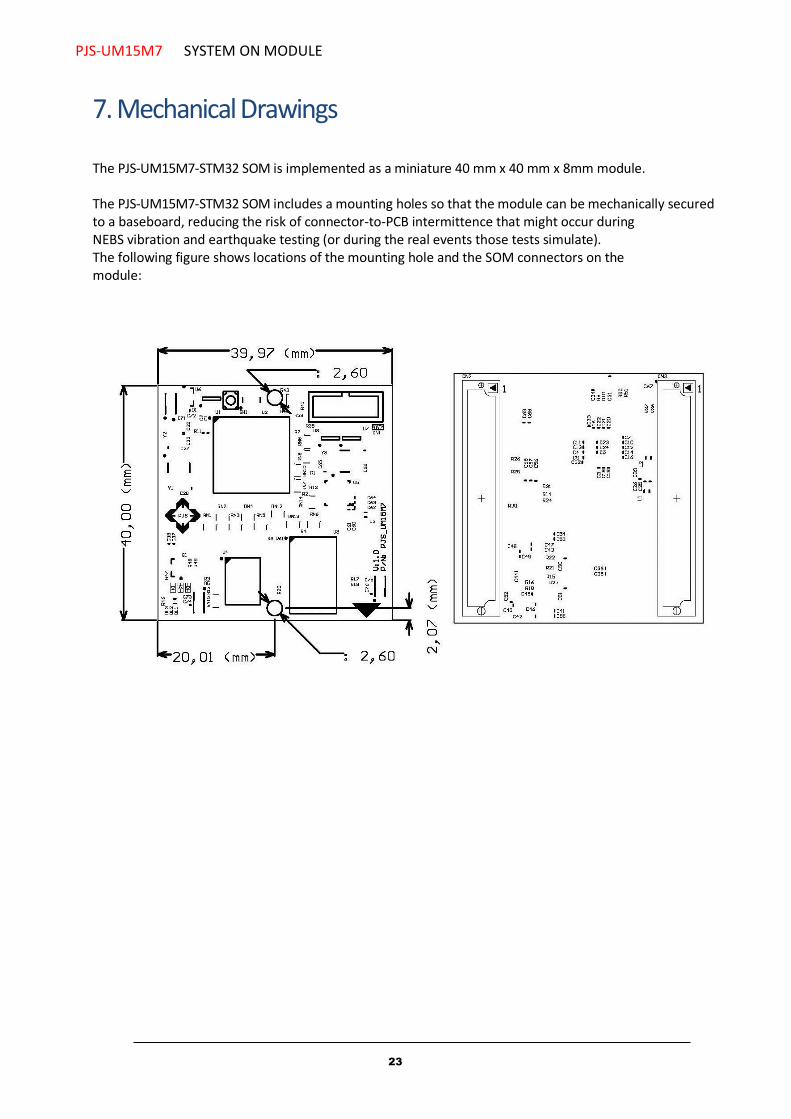
7. Mechanical Drawings The PJS-UM15M7-STM32 SOM is implemented as a miniature 40 mm x 40 mm x 8mm module. The PJS-UM15M7-STM32 SOM includes a mounting holes so that the module can be mechanically secured to a baseboard, reducing the risk of connector-to-PCB intermittence that might occur during NEBS vibration and earthquake testing (or during the real events those tests simulate). The following figure shows locations of the mounting hole and the SOM connectors on the module:

24
PJS-UM15M7 SYSTEM ON MODULE
12. Contact Information
Headquarters: Project Service S.a.s
31/C, Via Paderno Seriate, 24068 ITALY
Tel: +39-035-4520100 Fax: +39-035-4520731
Sales & Technical Support: [email protected]
Corporate Website: www.projectservice.it


