
Proceedings of International Conference Technology and Social Science 2018 (ICTSS 2018)
Pulse Coding Controlled Switching Converter with
Generating Automatic Frequency Tracking Notch
Characteristics for Radio Receiver
Yifei Sun1,a, Yi Xiong1,b, Yasunori Kobori1,c and Haruo Kobayashi1,d 1Division of Electronics and Informatics, Faculty of Science and Engineering, Gunma University
1-5-1 Tenjincho, Kiryu-shi, Gunma, 376-8515, Japan
a< [email protected] >, b<[email protected]>,
c<[email protected]>, d<[email protected]>
Keywords: spread spectrum, EMI reduction, notch frequency, pulse coding
Abstract. This paper proposes an EMI spread spectrum technique with automatic notch frequency
tracking using the pulse coding controlled method of the DC-DC switching converter for the
communication equipment. This proposed EMI spread spectrum technique does not distribute the
switching noise into some specified frequency bands. In other words, the noise spread spectrum
characteristics have selective notches. We can automatically prevent the noises from spreading into
important frequencies (such as AM, FM bands). The notches in the spectrum of the switching pulses
appear using two types of pulse coding method (PWC and PWPC). The notch frequency is
automatically set to that of the received signal by adjusting the clock frequency using the equation
Fn = (N + 0.5)Fck. Here Fn is a notch frequency, Fck is a clock frequency, N is a positive integer.
We have confirmed with simulation that the proposed technique is effective for EMI reduction and
notch generation.
1. Introduction
In recent years, with the acceleration of high-speed and high-frequency electronic equipment, the
fluctuation of the switching noise has strongly spread in the wide frequency range. So it is very
important to reduce Electro Magnetic Interference (EMI) noise by suppressing the peak levels at the
fundamental frequency and its harmonic frequencies. On the other hand, for the communication
equipment including the radio receiver, it is very important to reduce the radiation noise at the specific
frequencies, such as the receiving frequency, by suppressing diffusion of power supply noise. We have
proposed the pulse coding technique to have the notch characteristics in the noise spectrum of the
switching converter [1].
In this paper, we propose a spread spectrum technique for EMI reduction with suppressing diffusion
of power supply noise using Pulse Width Coding (PWC) and Pulse Width/Pulse Phase Coding (PWPC)
methods, based on the notch characteristics design. The notch frequency is automatically set to that of
the received signal by adjusting the clock frequency using the equation Fn = (N + 0.5)Fck. Then we
investigate the direct generation method of the clock and the coded pulses for automatic generation of
the notch frequency and also consider this notch frequency generation in the higher frequency range.
2. Switching Converters with Spread Spectrum
2.1 Basic DC-DC Switching Converters
Fig. 1 shows a basic block diagram of the buck type DC-DC converter [2,3] with the Pulse Width
Modulation (PWM) signal control and Fig. 2 shows its main signals. The comparator generates the
PWM signal by comparing a saw-tooth signal and the amplified error voltage as shown in Fig. 2. In

Proceedings of International Conference Technology and Social Science 2018 (ICTSS 2018)
500mV
1MHz
2.0V
50mV
1MHz
the buck type DC-DC converter, the output voltage Vo can be expressed by the following equation
using the input voltage Vi and the ON/OFF ratio D (Duty).
𝑉𝑜 = 𝐷 × 𝑉𝑖 (1)
Fig.1 Switching buck converter with PWM signal Fig.2 Waveform of switching buck converter
2.2 EMI Reduction and Pulse Width Coding (PWC) Method
In order to reduce the EMI noise, modulation of the clock pulse is usually used by shaking the phase
or frequency of the clock in Fig. 1. The spectrum of the PWM signal without the clock modulation is
shown in Fig. 3. There is the line spectrum at the frequency of the clock (0.2MHz) and there appear
many harmonic spectra. Fig. 4 shows the spectrum with the clock modulation. The peak level of the
clock spectrum is reduced from 3.5V to 2.0V which is 4.9dB reduction. There is no line spectrum but
the bottom levels of the spectrum are higher than 8mV. In Japan’s AM radio broadcasting, 0.5~1.6MHz
are used as the carrier frequency band, the occupied bandwidth of each broadcast station is 15kHz. In
other words, AM radio channel also diffuses noise to selected frequency. It is not good for the
communication devices which receive weak radio waves.
Fig.3 Simulated spectrum without EMI reduction Fig.4 Simulated spectrum with EMI reduction
In PWC method, the analog output voltage error is converted to a digital signal. By appropriately
switching and controlling the pulse width of this signal, the output voltage of the switching power
supply is stabilized. Parameters are defined to show the empirical formula of the notch frequency of
the PWC method. Let W be the width of pulse period, 𝑊𝐻 be the longer modulation width and 𝑊𝐿
be the shorter one. N represents a positive integer. At this time, the notch frequency Fn is expressed
by the following equation obtained by a numerical experiment.
𝐹𝑛 =𝑁
(𝑊𝐻−𝑊𝐿) (2)
3. Automatic Notch Frequency Generate with PWC Control
Fig.5 shows the control circuit for the PWC method switching converter. The output of this FF is
called a select signal (SEL) which selects one of the two pulses to the selector. These two pulses are
SAW
IL
CK
PWM
⊿V
V V
Frequency(MHz) Frequency(MHz)

Proceedings of International Conference Technology and Social Science 2018 (ICTSS 2018)
Coding Controller
SW E
Vo L
Di C
PWC
Q D
Modulated
Clock Pulse H
Pulse L
Select
SEL
⊿V
Vr
COMP
AMP
the coding pulses generated using the modulated clock. Here we manually set the value of 𝑊𝐻 and
𝑊𝐿. When tuning or switching communication channels, automatic adjustment to the input frequency
change is necessary. So we consider about automatic generation of Pulse-H and Pulse-L to realize
automatic PWC control.
3.1 Analysis of Relationship with Fck and Fn
Generally speaking, it is good for the notch frequency Fn to generate at the middle of Fck. When
the received signal frequency from a radio receiver is equal to the notch frequency, it is possible to
greatly reduce influence on other electronic devices. So we set the notch frequency equal to the
received signal frequency from radio receiver, that is input frequency Fin. The relationship is shown
in the next equation.
𝐹𝑖𝑛 = (𝑁 + 0.5) × 𝐹𝑐𝑘 [𝑁 = 𝑛𝑎𝑡𝑢𝑟𝑎𝑙 𝑛𝑢𝑚𝑏𝑒𝑟] (3)
On the other hand, the duty Do of the PWM signal in the switching converter is usually represented
like Do=Vo/Vin, here Vo is the output DC voltage and Vin is the input DC voltage respectively. Hence
the pulse width To of the PWM signal is represented as shown in Eq. (5). The period of the notch
frequency Tn is derived from the difference between the pulse widths of WH and WL. In this case, WH,
WL and To should have the relation shown in Eq. (6) in order to control the output voltage Vo to be
stable. Here, Tp is the pulse difference between WH and To or To and WL, and 2×Tp is equal to Tn;
this means the gain of the pulse coding control.
𝑇𝑜 = 𝐷𝑜 × 𝑇𝑐𝑘 =𝑉𝑜
𝑉𝑖𝑛× 𝑇𝑐𝑘 (4)
𝑊𝐻 = 𝑇𝑜 + 𝑇𝑝, 𝑊𝐿 = 𝑇𝑜 − 𝑇𝑝 (5)
𝑇𝑛 = 𝑊𝐻 − 𝑊𝐿 = 2 × 𝑇𝑝 (6)
3.2 Direct Generation of Clock Pulse (N=1)
In the Eq. (3), the period of clock Tck is able to be generated by measuring the period of the input
pulse Tin. It is easy to make Tck with a shifter and a digital adder in digital circuit. Fig. 6 is automatic
PWC method pulse coding circuit according to Eq. (4)~(6) when 𝐷𝑜 = 0.5 situation.
Fig.5 Converter with PWC control Fig.6 Automatic PWC method of the direct method
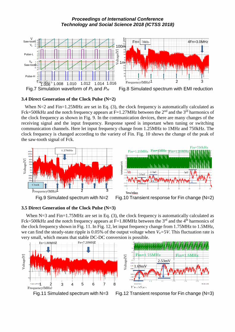
3.3 Simulation Result of the Direct Method (N=1)
Fig. 7 shows the simulation waveforms of PL and PH if we just set Fin equal to 750kHz. Tck is the
saw-tooth, compared with VL and VH can produce Pulse-L and Pulse-H automatically. The simulated
spectrum of the direct method is shown in Fig. 8. The notch characteristics can be clearly reflected.
The frequency is 750kHz which is equal to Fin. The bottom level of the notch frequency is 1mV. There
appears another big notch at F=3.0MHz, which is the 4th harmonic of the fundamental notch frequency.
Proceedings of International Conference Technology and Social Science 2018 (ICTSS 2018)
Fig.7 Simulation waveform of PL and PH Fig.8 Simulated spectrum with EMI reduction
3.4 Direct Generation of the Clock Pulse (N=2)
When N=2 and Fin=1.25MHz are set in Eq. (3), the clock frequency is automatically calculated as
Fck=500kHz and the notch frequency appears at F=1.27MHz between the 2nd and the 3rd harmonics of
the clock frequency as shown in Fig. 9. In the communication devices, there are many changes of the
receiving signal and the input frequency. Response speed is important when tuning or switching
communication channels. Here let input frequency change from 1.25MHz to 1MHz and 750kHz. The
clock frequency is changed according to the variety of Fin. Fig. 10 shows the change of the peak of
the saw-tooth signal of Fck.
Fig.9 Simulated spectrum with N=2 Fig.10 Transient response for Fin change (N=2)
3.5 Direct Generation of the Clock Pulse (N=3)
When N=3 and Fin=1.75MHz are set in Eq. (3), the clock frequency is automatically calculated as
Fck=500kHz and the notch frequency appears at F=1.80MHz between the 3rd and the 4th harmonics of
the clock frequency shown in Fig. 11. In Fig. 12, let input frequency change from 1.75MHz to 1.5MHz,
we can find the steady-state ripple is 0.05% of the output voltage when Vo=5V. This fluctuation rate is
very small, which means that stable DC-DC conversion is possible.
Fig.11 Simulated spectrum with N=3 Fig.12 Transient response for Fin change (N=3)
Saw-tooth
Saw-tooth
V𝐿
V𝐻
Pulse-L
Pulse-H
Fn= 4Fn=3.0MHz
Voltage[V]
1
100m
1m
Frequency(MHz) 1 2 3 1.006 1.008 1.010 1.012 1.014 1.016
V
Voltage[V]
1 2 3 Frequency(MHz)
Voltage[V]
Frequency(MHz) 2 1 3 4 5 6 7 8
Fn=1.80MHz Fn=7.20MHz
2.53mV
1.69mV
Fin=1.75MHz Fin=1.5MHz
Voltage[V]
Fin=1.25MHz Fin=1MHz
Fin=750kHz
Fin=1.25MHz

Proceedings of International Conference Technology and Social Science 2018 (ICTSS 2018)
Fig.13 Simulated spectrum in high frequency (N=3) Fig.13 shows simulated spectrum in high frequency regions from 75MHz to 85MHz situation. In
high frequency regions, the harmonics notch is not clear, but it is still good for AM radio receiver as
we mentioned earlier because in AM radio broadcasting, 0.5~1.6MHz are used as the carrier frequency
band. In order to generate notches at high frequency, we come up with PWPC method.
4. Automatic Generating of Notch Frequency with PWPC Control
The PWPC method is a modulation method combined with PWC (Pulse Width coding) and PPC
(Pulse Phase Coding) methods. We consider the automatic generation of Pulse-H and Pulse-L and
Pulse-LD (Fig.14) to realize an automatic PWPC control.
Fig.14 Pulse coding of PWPC method Fig.15 Coding pulse list
From Fig. 15, parameters are defined to show the empirical formula of the notch frequency. Let τ
be the delay of pulse coding, τ𝐻 be the longer delay and τ𝐿 be the shorter one. N is represents a
positive integer. At this time, the notch frequency Fn is expressed by the following equation obtained
by a numerical experiment
𝐹𝑛 =𝑁
2(𝜏𝐻−𝜏𝐿) (7)
4.1 Analysis of PWPC Method
In PWPC method, the notch frequency can be realized by the Eq. (2) and Eq. (7), these two equations
are made to obtain a big notch. Fig.14 shows a configuration of PWPC system. Using PWPC method,
we want to produce delay saw-tooth compared with 𝑉𝐿 to create Pulse-LD.
Fig. 16 Design timing in PWPC method Fig. 17 Main waveforms of Fig. 14
Voltage[V]
Frequency(MHz) 78 80 82 84
44Fn=77MHz 45Fn=78.75MHz 46Fn=80.5MH
z
47Fn=82.25M
Hz
48Fn=84MHz
Tck
VL
VL
WL
WL
τ
τ
PL
PLD
Tck
V
V
V
Pulse-H
Pulse-L
Pulse-LD

Proceedings of International Conference Technology and Social Science 2018 (ICTSS 2018)
Fig.16 shows the designed timing in PWPC method, where the phase shift τ is equal to 0.5Tin if
Eq.(2) is equal to Eq.(7) in order to create big notch.
𝜏 = (𝑊𝐻-𝑊𝐿)/2 = 0.5 × 𝑇𝑖𝑛 (8)
4.2 Automatic Generation of Notch Frequency with PWPC Control
Fig.17 shows major signal waveforms in Fig. 14. The coding pulses 𝑃𝐻, 𝑃𝐿 or 𝑃𝐿𝐷 are generated
by comparing the voltage (𝑇𝑜 + 𝑇𝑝), (𝑇𝑜 − 𝑇𝑝) or (𝜏 + 𝑇𝑜 − 𝑇𝑝) with the saw-tooth signal Tck.
In the proposed system, the input/output voltage are Vin=10V and Vo=5V, so that the theoretical
duty ratio of the signal is Do=0.5. When the frequency of the input signal is set at Fin=750kHz, and in
N=1 situation, the frequency of the clock is guided at Fck=500kHz by Eq. (3). In order to set the notch
frequency at Fin=750kHz, the calculated pulse widths are chosen as 𝑊𝐻=1.67μs, 𝑊𝐿 = 0.33μs, and
the delay time is 𝜏=0.67μs.
Seeing the simulation results, the simulated widths of the coded pulses are set to 𝑊𝐻=1.65μs,𝑊𝐿 =0.35μs , 𝜏=0.67μs as shown in Fig. 17. In this case, the simulated notch frequency appears at
Fn=750kHz shown in Fig.18, which is almost equal to the theoretical notch frequency Fin=750kHz.
There appears a big notch at F=3.0MHz, which is the 4th harmonic of the fundamental notch frequency
Fn. The output voltage ripple is 3.98mV as shown in Fig. 19.
Fig.18 Simulation spectrum with PWPC control (N=1) Fig.19 Simulated output voltage ripple
5. Conclusion
This paper has proposed a technique to generate the notch characteristics at the desired frequency
in the noise spectrum of the switching converter. The clock pulse and the coding pulses are
automatically generated and the notch characteristic automatically appears at the input frequency
where the notch frequency Fn appears between the clock frequency Fck and its 2nd harmonic or the 2nd
and the 3rd harmonics. We have confirmed with simulation that automatic notch generation in noise
spectrum of switching converters with PWC and PWPC methods can be achieved. It is good for radio
receivers to receive high frequency signal without other communication device interferences.
References
[1] H. Kobayashi, T Nabeshima, Handbook of Power Management Circuits, Pan Stanford Publishers, 2016.
[2] Y. Kobori, N. Tsukiji, N Arafune, M. W. S. Dulara, Y. Sun, N. Takai, H. Kobayashi, "Noise Spread
Spectrum with Adjustable Notch Frequency in Complex Pulse Coding Controlled DC-DC Converters",
IEEE International Symposium on Intelligent Signal Processing and Communication Systems 2017, NP-
L5, Xiamen, China (Nov. 2017)
[3] Y. Sun, Y. Xiong, N. Tsukiji, Y. Kobori, H. Kobayashi, “Self-adjustable Notch Frequency in Noise
Spectrum of Pulse Coding DC-DC Converter for Communication Devices”, International Conference on
Electrical and Medical Intelligent System (ICMEMIS), IPS01-03, Kiryu, Japan (Nov. 2017)
Frequency(MHz)
Voltage[V]
750kHz 4Fn=3MHz 8Fn=6MHz 12Fn=9MHz
2 0 4 6 8 10
3.98mV
Voltage[V]


