
Radiation Hardened Electronics Destined for Severe Nuclear Reactor Environments
Keith E. Holbert and Lawrence T. ClarkArizona State University
September 18, 2014
Award Number DE-NE0000679
2
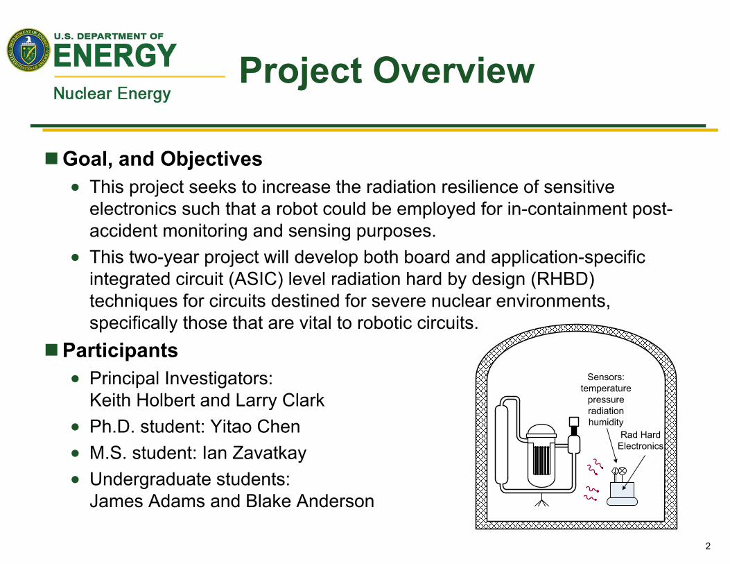
Project Overview
Goal, and Objectives This project seeks to increase the radiation resilience of sensitive
electronics such that a robot could be employed for in-containment post-accident monitoring and sensing purposes.
This two-year project will develop both board and application-specific integrated circuit (ASIC) level radiation hard by design (RHBD) techniques for circuits destined for severe nuclear environments, specifically those that are vital to robotic circuits.
Participants Principal Investigators:
Keith Holbert and Larry Clark Ph.D. student: Yitao Chen M.S. student: Ian Zavatkay Undergraduate students:
James Adams and Blake Anderson
Sensors:temperature
pressureradiationhumidity
Rad Hard Electronics
3
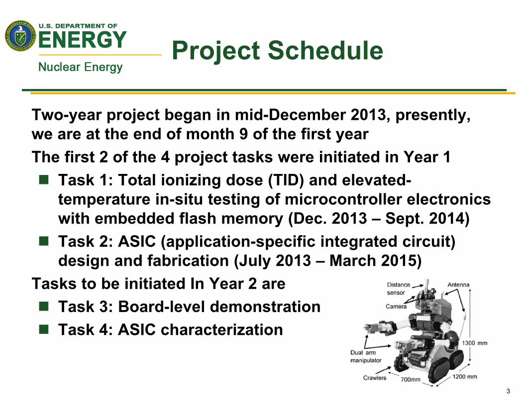
Project Schedule
Two-year project began in mid-December 2013, presently, we are at the end of month 9 of the first yearThe first 2 of the 4 project tasks were initiated in Year 1 Task 1: Total ionizing dose (TID) and elevated-
temperature in-situ testing of microcontroller electronics with embedded flash memory (Dec. 2013 – Sept. 2014)
Task 2: ASIC (application-specific integrated circuit) design and fabrication (July 2013 – March 2015)
Tasks to be initiated In Year 2 are Task 3: Board-level demonstration Task 4: ASIC characterization
4
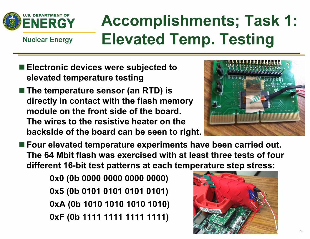
Accomplishments; Task 1: Elevated Temp. Testing
Electronic devices were subjected to elevated temperature testing
The temperature sensor (an RTD) is directly in contact with the flash memory module on the front side of the board. The wires to the resistive heater on the backside of the board can be seen to right.
Four elevated temperature experiments have been carried out. The 64 Mbit flash was exercised with at least three tests of four different 16-bit test patterns at each temperature step stress:
0x0 (0b 0000 0000 0000 0000)0x5 (0b 0101 0101 0101 0101)0xA (0b 1010 1010 1010 1010)0xF (0b 1111 1111 1111 1111)

5
Accomplishments; Task 1: Elevated Temp. Testing
The bits were monitored for errors as well as error direction, 0 to 1 and 1 to 0. The first error was observed at 145 °C, which is 20°C above the manufacturer stated maximum stress limit.
The elevated temperature testingrevealed the read operation induces 1 to 0 failures whileerase/programming causes0 to 1 changes.
Hence, the memory can beread reliably at temperatures significantly higher thanthe 125°C rating, that is,programs can be continuedto be executed in harshenvironmental conditions.
0
200,000
400,000
600,000
800,000
1,000,000
1,200,000
140 150 160 170 180
Bits
in E
rror
Temperature (°C)
Elevated Temperature Experiment 3
0xF 1-00x5 1-00xA 1-0
6
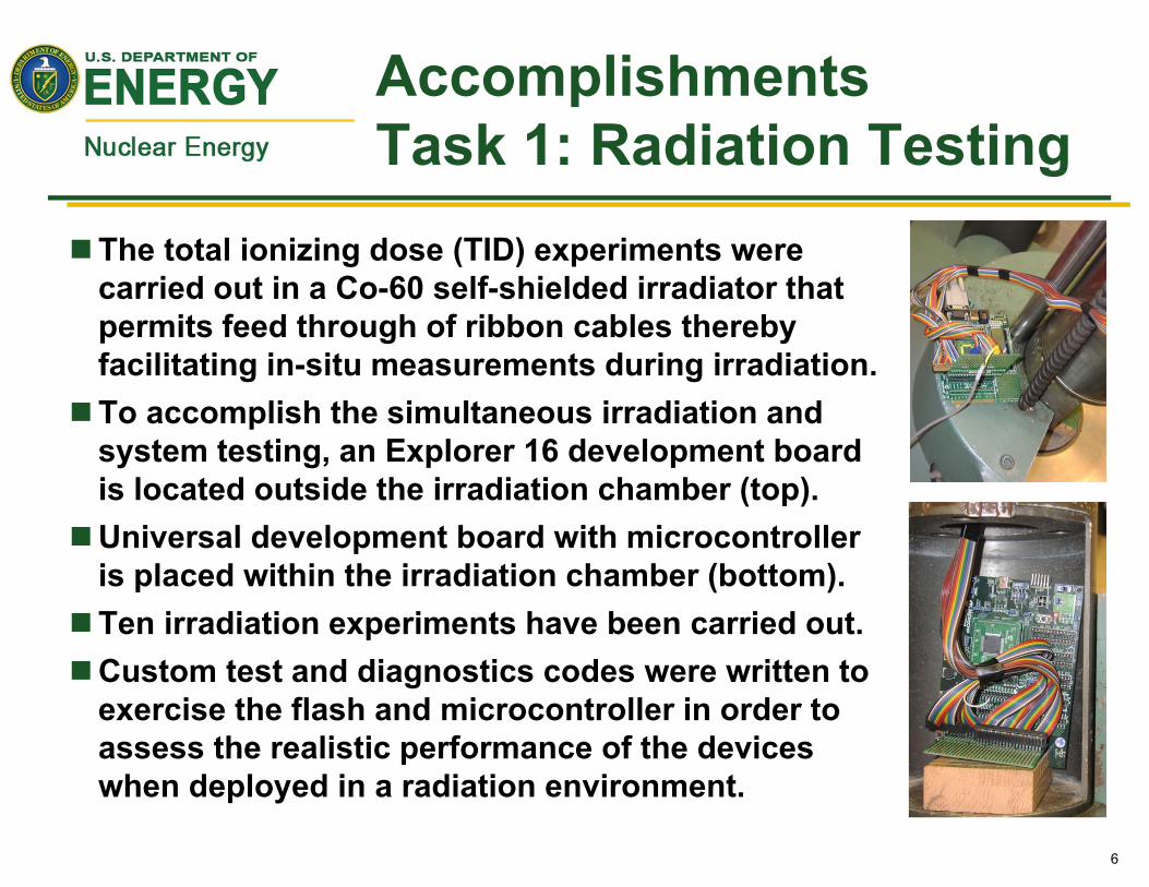
AccomplishmentsTask 1: Radiation Testing
The total ionizing dose (TID) experiments were carried out in a Co-60 self-shielded irradiator that permits feed through of ribbon cables thereby facilitating in-situ measurements during irradiation.
To accomplish the simultaneous irradiation and system testing, an Explorer 16 development board is located outside the irradiation chamber (top).
Universal development board with microcontroller is placed within the irradiation chamber (bottom).
Ten irradiation experiments have been carried out. Custom test and diagnostics codes were written to
exercise the flash and microcontroller in order to assess the realistic performance of the deviceswhen deployed in a radiation environment.

7
AccomplishmentsTask 1: Radiation Testing
As an example test regime: the 64 Mbit chip is divided into four sectors of 16 Mb each
The individual sectors were programmed for different operations and intervals
Sector A: reprogram and read every 30 min (15 krad);Sector B: read only every 60 min beginning at 90 min; andSector C: read only 60 m.
Each 16 Mb sector was then further divided into 32 unique tests (right)specific to the experiment.
Lots of data for analysis.
8
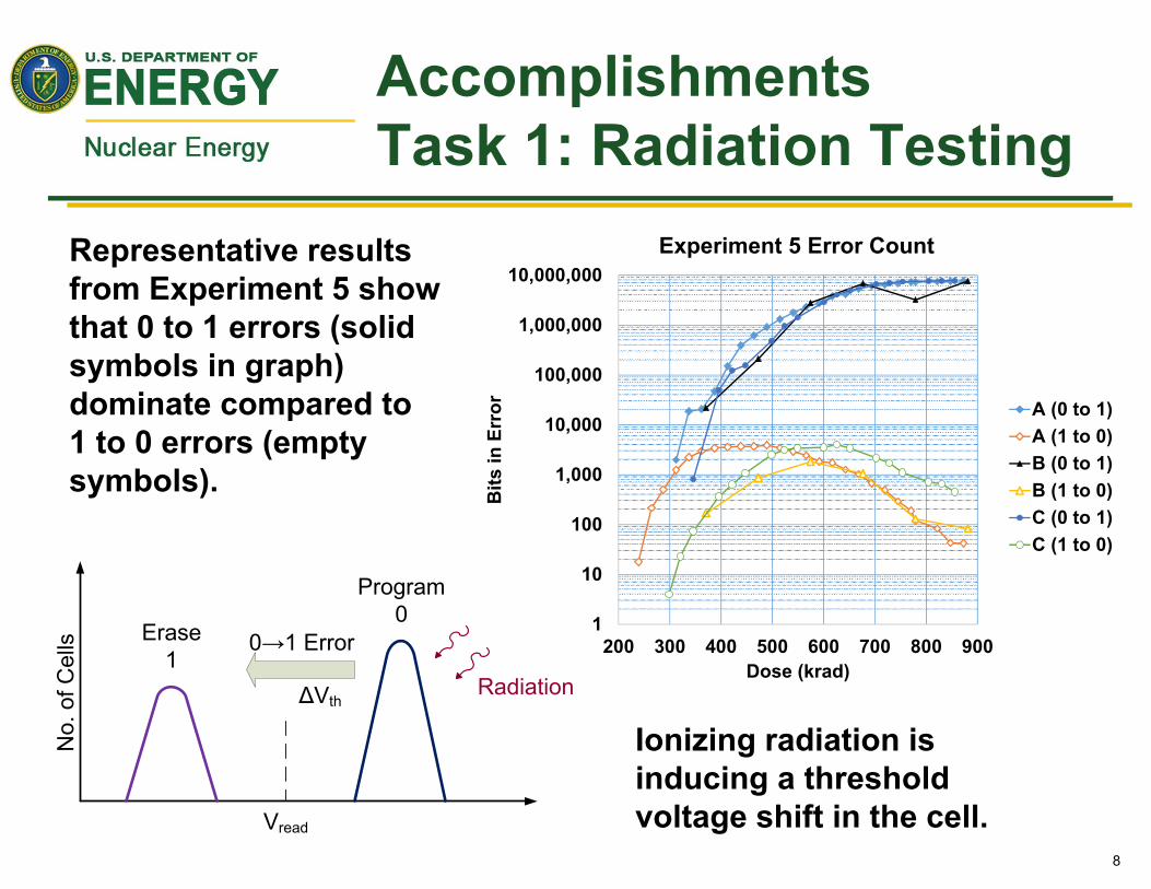
AccomplishmentsTask 1: Radiation Testing
Representative results from Experiment 5 show that 0 to 1 errors (solid symbols in graph) dominate compared to 1 to 0 errors (empty symbols).
1
10
100
1,000
10,000
100,000
1,000,000
10,000,000
200 300 400 500 600 700 800 900
Bits
in E
rror
Dose (krad)
Experiment 5 Error Count
A (0 to 1)A (1 to 0)B (0 to 1)B (1 to 0)C (0 to 1)C (1 to 0)
Ionizing radiation is inducing a threshold voltage shift in the cell.Vread
Erase1
Program0
Radiation∆Vth
0→1 Error
No.
of C
ells
9
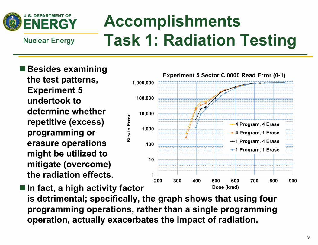
1
10
100
1,000
10,000
100,000
1,000,000
200 300 400 500 600 700 800 900
Bits
in E
rror
Dose (krad)
Experiment 5 Sector C 0000 Read Error (0-1)
4 Program, 4 Erase
4 Program, 1 Erase
1 Program, 4 Erase
1 Program, 1 Erase
AccomplishmentsTask 1: Radiation Testing
Besides examining the test patterns, Experiment 5undertook to determine whether repetitive (excess) programming or erasure operations might be utilized to mitigate (overcome)the radiation effects.
In fact, a high activity factoris detrimental; specifically, the graph shows that using four programming operations, rather than a single programming operation, actually exacerbates the impact of radiation.

10
AccomplishmentsTask 1: Radiation Testing
Although the flash testing has shown operability to doses of a few hundred krad, the commercial off-the-shelf (COTS) 16-bit and 32-bit microcontrollers have exhibited less radiation resilience than expected (<100 krad); consequently, we are evaluating an 8-bit processor that also utilizes the proven SuperFlash that we have successfully tested.
Preliminary conclusions indicate failure mechanisms of: (1) 0→1 fails are due to cell leakage and access device, i.e., word line, leakage; (2) (sensing) failure causes 1→0; (3) a less predictable degradation mechanism may be due to charge pump failure.
Besides using radiation hard by design (RHBD) to increase the dose for failure onset, effort should be expended to implement error detection and correction (EDAC) to further mitigate the radiation-induced effects.

11
eFlash Irradiation Failure Mechanisms
SuperFlash is a 1.5T cell Circuit model is two series transistors
– Floating gate (FG) to source (grounded at read) in series with access device (MA1)
Drain = bitline
Vread
Erase1
Program0
Radiation∆Vth
0→1 Error
Logic state 1 (on) 0 (off)Threshold, Vth Low HighOperation Erase ProgramFloating gate Conducting Non-conducting

12
eFlash Irradiation Failure Mechanisms
Primary 0-1 failure mechanism is access transistor (MA1, MA2) leakage Clearly proportional to read access rate
If FG is programmed off ‘0’ (charged to high Vth) it blocks the current flow Bits programmed to 0 do not contribute to
fails, but can fail—the off FG device blocks the TID induced current path through MA
If FG is programmed on ‘1’ (erased to low Vth, conducting state) it does not obstruct the TID induced leakage path Bits programmed to 1 contribute to fails on
LBL, but themselves cannot fail due to leakage—TID induced leakage discharges the bitline (as would the read) so these cells read correctly in that case
on (conducts)
off
‘0’
‘1’

13
AccomplishmentsTask 2: ASIC Design
90-nm (TSMC LP) eFlash test chip Contains two SST eFlash macros
– eFlash macros have separate power supplies to determine TID impact independent of the surrounding logic
– Also incorporates EDAC and power gating features to investigate possibility of correction
Separate on-die NMOS and PMOS power gating structures to determine viability of gating flash power for longer TID lifetime
This effort was co-sponsored by Space Micro Microchip Inc. supported the tape-out
TSMC: Taiwan Semiconductor Manufacturing Company; LP: low powerSST: Silicon Storage Technology (a Microchip company)
14
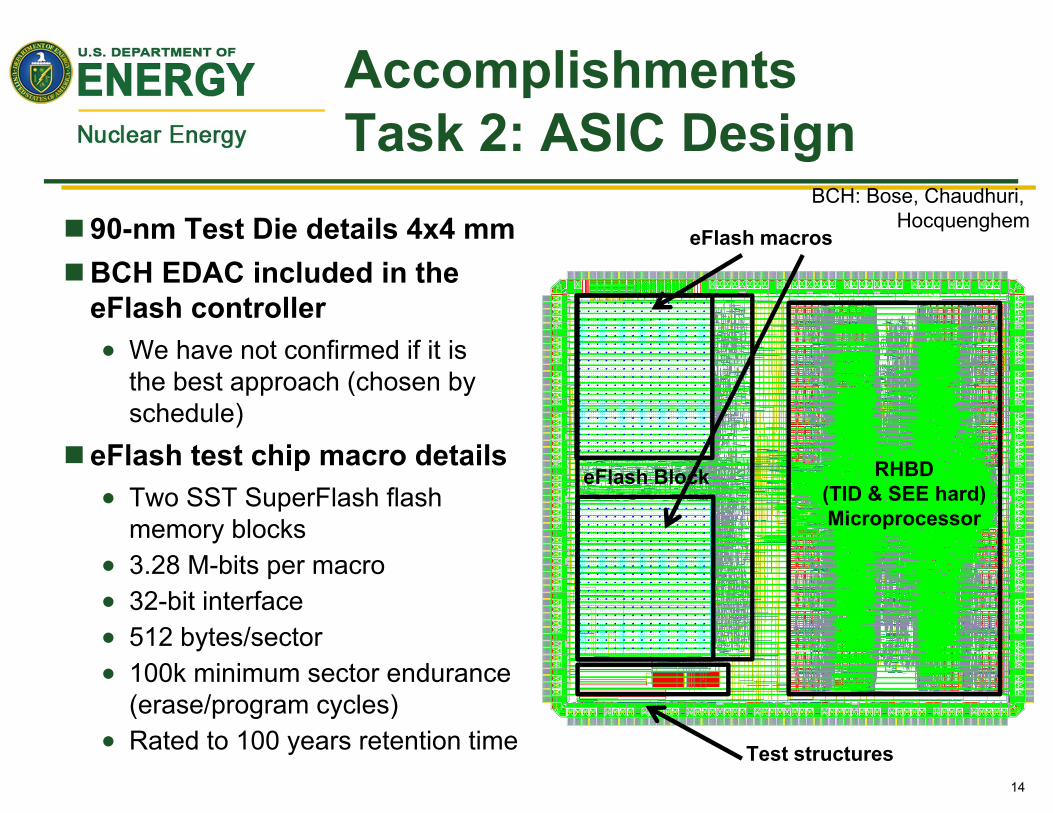
AccomplishmentsTask 2: ASIC Design
90-nm Test Die details 4x4 mmBCH EDAC included in the
eFlash controller We have not confirmed if it is
the best approach (chosen by schedule)
eFlash test chip macro details Two SST SuperFlash flash
memory blocks 3.28 M-bits per macro 32-bit interface 512 bytes/sector 100k minimum sector endurance
(erase/program cycles) Rated to 100 years retention time
eFlash macros
eFlash Block RHBD (TID & SEE hard) Microprocessor
Test structures
BCH: Bose, Chaudhuri, Hocquenghem

15
Technology Impact
The methods being developed in this work will facilitate the long-term viability of radiation-hard electronics and robotic systems, thereby avoiding obsolescence issues. We are determining (physics based) specific failure
mechanisms for eFlash arrays (prior work has been behavior based).We have correlated the mechanisms between temperature
and radiation effects (both of which involve leakage).Determining limits to the technology and understanding
the exact mechanisms allows better determination of the value of different system level mitigation approaches.This technology not only has applicability to severe
accident conditions but also to facilities throughout the nuclear fuel cycle in which radiation tolerance is required.
16
Conclusion
Ionizing radiation is intrinsic to the entire nuclear energy fuel cycle. The pervasive use of electronic systems demands devices that can withstand significant radiation exposure. The nuclear power industry needs to be able to benefit from the advancements in the semiconductor industry which have led to low-cost ubiquitous devices. This project is contributing to the deployment of state-of-the-art electronics that can improve the reliability, sustain the safety, and extend the life of current reactors.The full station blackout experience at Fukushima shows
the necessity for emergency sensing capabilities in a radiation-enhanced environment. This project serves to develop radiation-hard-by-design (RHBD) electronics.


