

1.
Revision History
Page 3
2. General Specification 4 3. Module Coding System 5 4. Interface Pin Function 6 5. Outline dimension & Block Diagram 7 6. Display Control Instruction 9 7. Optical Characteristics 10 8. Absolute Maximum Ratings 13 9. Electrical Characteristics 13 10. Backlight Information 18 11. Reliability 19 12. Cosmetic Criteria of LCD Screen 21 13. Precautions in use of LCD Modules 24 14. Material List of Components for RoHs 25
1. Revision History

DATE VERSION REVISED PAGE NO. Note
2009/08/06
1
First issue
2. General Specification

This product is composed of a TFT LCD panel, driver ICs, FPC, Control Board and a
backlight unit. The following table described the features of MCT035K6W320240LML.
Dot Matrix: 320 x RGB x240
Module dimension: 93.5 x 66.44 x 7.96 (max.) mm3
View area: 73.1x55.6 mm2
Active area: 70.08 x 52.56 mm2
Dot size: 0.073 x 0.219 mm2
LCD type: TFT, Negative, Transmissive
View direction: 6 o’clock
Backlight Type: LED, Normally White
Controller IC: SSD1963
Driving IC package: COG
*Expose the IC number blaze (Luminosity over than 1 cd) when using the LCM may cause IC operating failure.
*Color tone slight changed by temperature and driving voltage.
3. Module Coding System

Midas Active Matrix Display Part Number System
MC T 057 A 6 * W 320240 L M L * * * * *1 2 3 4 5 6 7 8 9 10 11 12 13 14 15 16
1 = MC: Midas Components
2 = T: TFT A: Active Matrix OLED
3 = Size
4 = Series
5 = Viewing Angle: 6: 6 O’clock 12: 12 O’clock
6 = Blank: No Touch T: Touchscreen
7 = Operating Temp Range: S: 0 to 50Deg C B: -20+60Deg C W: -20+70Deg C E: -30+85Deg C
8 = No of Pixels
9 = Orientation: P: Portrait L: Landscape 10 = Mode: R: Reflective M: Transmissive T: Transflective S: Sunlight Readable (transmissive) 11 = Backlight: Blank: None L: LED C: CCFL 12 = Blank: No Module/board C: Controller board module
13 = Blank: None V: Video
14 = Blank: None B: Bracket
15 = Blank: None H: Host Cable
16 = Blank: None K: Keyboard

Pins Connection to Control Board P/N Symbol 8BIT Function 1 GND Ground 2 VCC Power supply for Logic 3 BL_E Backlight control (H: On \ L: Off) 4 RS Command/Data select 5 WR 8080 family MPU interface : Write signal6 RD 8080 family MPU interface: Read signal7 DB0 8 DB1 9 DB2
10 DB3 11 DB4 12 DB5 13 DB6 14 DB7
Data bus
15 CS Chip select 16 RES REST 17 NC No connection 18 FGND Frame Gnd 19 NC No connection 20 NC No connection
5. Outline Dimension & Block Diagram

CON1
2.74
4.26
55.6
(VA
)52
.56(
AA
)
79.12
70.08(AA)
86
546.
22
73.1(VA)
66.4
4
4-O3.5 PTH
4.52
3.01
93.5
3.757.19
1
(Down-Side)CN-FPC-54P/P0.5
48.5673.278.2
2.5
6065
(PC
B)
2.5
4-O5.0PAD4-O2.5PTH
68.65
7.96
J3
CON1
CSDB7DB6
RESNC
FGNDNC
DB512
1413
VSS1
7
1110
89
4
65
32
RDWRRS
1617
1920
18
15
VCCBL_E
DB0DB1DB2DB3DB4
NC
CN-FPC-20P/P1.0(Up-Side)
5.06

TFT ARRAY/CELL
6 bits data
for R/G/B Hs Vs
Vcc(3.3V)
Backlight Unit LED( 6 DICE)
320(R/G/B) X 240
GND
SSD1963
Contralsignal
CLK
Data Bus 18bit 16bit
9bit 8bit
Power Circuit
BackLightCircuit
3.3 to 5.0(VDD)Regulator
6. Display Control Instruction

6.1 Data transfer order Setting
Pixel Data Format Both 6800 and 8080 support 8-bit, 9-bit, 16-bit, 18-bit and 24-bit data bus. Depending on the width of the data bus, the display data are packed into the data bus in different ways.
Pixel Data Format:
6.2 Register Depiction
Please consult the spec of SSD1963

7. Optical Characteristics
Note 2: Test equipment setup: After stabilizing and leaving the panel alone at a driven temperature for 10 minutes, the measurement should be executed. Measurement should be executed in a stable, windless, and dark room. Optical specifications are measured by Topcon BM-7 luminance meter 1.0° field of view at a distance of 50cm and normal direction.

Note 3: Definition of Response time: The response time is defined as the LCD optical switching time interval between “White” state and “Black” state. Rise time, Tr, is the time between photo detector output intensity changed from 90﹪to 10﹪. And fall time, Tf, is the time between photo detector output intensity changed from10﹪to 90﹪.
Note 4: Definition of contrast ratio: The contrast ratio is defined as the following expression.

Note 5: White Vi = Vi50 ± 1.5V Black Vi = Vi50 ± 2.0V “±” means that the analog input signal swings in phase with VCOM signal. “±” means that the analog input signal swings out of phase with VCOM signal. The 100% transmission is defined as the transmission of LCD panel when all the input terminals of module are electrically opened. Note 6: Definition of color chromaticity (CIE 1931) Color coordinates measured at the center point of LCD Note 7: Measured at the center area of the panel when all the input terminals of LCD panel are electrically opened.

8. Absolute Maximum Ratings
Item Symbol Min Typ Max Unit
Operating Temperature TOP -20 - +70
Storage Temperature TST -30 - +80
VGH -0.3 - 32.0 V
VGL -22.0 - 0.3 VPower Voltage
VGH - VGL -0.3 - +45 V
Input voltage Vin -0.5 - 4.6 V
Logic output Voltage VOUT -0.5 - 4.6 V
Note: Device is subject to be damaged permanently if stresses beyond those absolute maximum ratings listed above
9. Electrical Characteristics
Operating conditions: Item Symbol Condition Min Typ Max Unit
Supply Voltage For
Logic VCC - 3.0 3.3 3.6 V
VGH Ta=25 15 V Power Supply Voltage
VGL Ta=25 -10 V
Supply Current Icc VCC=3.3 213 mA
(*NOTE1)
*Note1:VcomH& VcomL:Adjust the color with gamma data.

DC CHARATERISTICS Conditions: Voltage referenced to VSS VDDD, VDDPLL = 1.2V VDDIO, VDDLCD = 3.3V TA = 25°C
DC Characteristics Symbol Parameter Test Condition Min Typ Max Unit PSTY Quiescent
Power 300 uW
IIZ Input leakage current
-1 1 uA
IOZ Output leakage current
-1 1 uA
VOH Output high voltage
0.8VDDIO V
VOL Output low voltage
0.2VDDIO V
VIH Input high voltage
0.8VDDIO VDDIO + 0.5
V
VIL Input low voltage
0.2VDDIO V

AC Characteristics Conditions: Voltage referenced to VSS
VDDD, VDDPLL = 1.2V VDDIO, VDDLCD = 3.3V TA = 25 C CL = 50pF (Bus/CPU Interface) CL = 0pF (LCD Panel Interface)
9.1Clock Timing Clock Input Requirements for CLK (PLL-bypass)
Symbol Parameter Min Max Units FCLK Input Clock Frequency
(CLK) 120 MHz
TCLK Input Clock period (CLK) 1/fCLK ns Clock Input Requirements for CLK (Using PLL)
Symbol Parameter Min Max Units FCLK Input Clock Frequency
(CLK) 2.5 50 MHz
TCLK Input Clock period (CLK) 1/fCLK ns Clock Input Requirements for crystal oscillator XTAL (Using PLL)
Symbol Parameter Min Max Units FXTAL Input Clock Frequency 2.5 10 MHz TXTAL Input Clock period 1/fXTAL ns
9.2 MCU Interface Timing 9.2.1 6800 Mode
6800 Mode Timing Symbol Parameter Min Typ Max Unit tcyc Reference Clock Cycle Time 9 - - ns tPWCSL Pulse width CS# or E low 1 - - tCYC tPWCSH Pulse width CS# or E high 1 - - tCYC tFDRD First Data Read Delay 5 - - tCYC tAS Address Setup Time 1 - - ns tAH Address Hold Time 1 - - ns tDSW Data Setup Time 4 - - ns tDHW Data Hold Time 1 - - ns tDSR Data Access Time - - 5 ns tDHR Output Hold time 1 - - ns

Figure9-1: 6800 Mode Timing Diagram (Use CS# as Clock)
Figure 9-2: 6800 Mode Timing Diagram (Use E as Clock)

9.2.2 8080 Mode Write Cycle Table 9-5: 8080 Mode Timing Symbol Parameter Min Typ Max Unit tcyc Reference Clock Cycle Time 9 - - ns tPWCSL Pulse width CS# low 1 - - tCYC tPWCSH Pulse width CS# high 1 - - tCYC tFDRD First Read Data Delay 5 - - tCYC tAS Address Setup Time 1 - - ns tAH Address Hold Time 1 - - ns tDSW Data Setup Time 4 - - ns tDHW Data Hold Time 1 - - ns tDSR Data Access Time - - 5 ns tDHR Output Hold time 1 - - ns Figure9-3: 8080 Mode Timing Diagram

10. Backlight Information
Note 2 : Ta = 25 _ Note 3 : Brightness to be decreased to 50% of the initial value

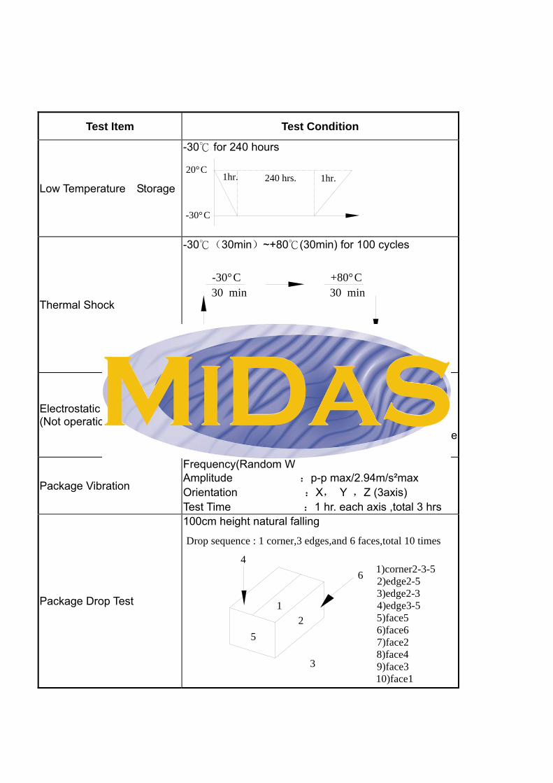
11.Reliability
Test Item Test Condition
High Temperature Operation
70 for 240 hours
1hr 240hrs 1hr
70°C
20°C
High Temperature Operation Humidity Operation
60 ,90%RH for 240 hours
1hr 1hr
240 hrs
90%R.H60°C
20°C
Low Temperature Operation
-20 for 240hours
1hr. 240 hrs. 1hr.20°C
-20°C
High Temperature Storage
80 for 240 hours
1hr 240hrs 1hr
80°C
20°C
Test Item Test Condition
Low Temperature Storage
-30 for 240 hours
1hr. 240 hrs. 1hr.20°C
-30°C
Thermal Shock
-30(30min)~+80 (30min) for 100 cycles
30 min 30 min
1cycle;repeat 100 cycles
-30°C +80°C
Electrostatic Discharge (Not operation)
Discharge Resistance :330Ω Energy Storage Capacitor :150pF Output voltage (1)Contact Discharge ±4KV (2)Air Discharge ±8KV Polarity of the output voltage :positive and negativeDischarge times :5times
Package Vibration
Frequency(Random W
ave)·10HZ~55HZ~10HZ
Amplitude :p-p max/2.94m/s²max Orientation :X, Y ,Z (3axis) Test Time :1 hr. each axis ,total 3 hrs
Package Drop Test
100cm height natural falling
6
1
52
3
4
Drop sequence : 1 corner,3 edges,and 6 faces,total 10 times
1)corner2-3-52)edge2-53)edge2-34)edge3-55)face56)face67)face28)face49)face310)face1

12. Cosmetic Criteria of LCD Screen 12.1 Inspection Condition Sample Plan:MIL-STD-105E LEVEL: II AQL: Major (MA):0.65%/Minor(MI):1.5% Cosmetic inspect 300~500Lux fluorescent light, leaving 30~35cm between panels and
eyes ,and between panels and lights. Functional in spec under 200 Lux . Inspection condition is 23±5 ,50±20%RH maximum.
Panel
fluorescent light
eye
eye
30cm
·Definition of area
A Area
B Area
A Area: Viewing area. B Area: Out of viewing.(Don’t care cosmetic in outside viewing area)

12.2 Inspection specification NO Item Acceptable specification Judgment
Criterion
1 Electrical Testing (MA)
1-1 sub pixel classification sub pixel: Number of sub pixel doesn’t exceed
Five dot.
Sub Pixel(Dot)
a>Dark dot ----Four Allowed b>Bright dot---one Allowed c>The definition of dot ----The size of a defective dot
over 1/2 of whole dot is regarded as one defective dot.
d> Dark sub pixel: The distance more than 5mm between dot and dot.
e>Bright sub pixel: The distance more than 20mm between bright dot and bright dot .
Pixel : Three dots link together-----one allowed.
Pixel
1-2Leakage to light Leakage to light be not allowed. 1-3 Picture to shake Picture had shake ,twinkle and noise etc. instable of defect that be not allowed. 1-4 Function No display or No function is not allowed. Source Line, Gate Line is not allowed. Contrast Ratio exceeds product specifications. Current consumption exceeds product specifications. Display malfunction.
N≤4 N≤1 N≤1 N=0 N=0 N=0
02 Mechanical
Dimension(MA)
2.1 Mechanical Dimension exceeds product
specifications. 2-2 Out of frame and boss of plastic changed shape
that be not allowed.
N=0

NO Item Acceptable specification Judgment Criterion
3 Cosmetic Inspection(MA)
3-1 Fiber / Line shapes of defect
L: length(mm) W: width(mm)
L
W
3-2 Blemish: dot shapes of defect.
3-3 Bubble
Foreign Substances
a
b
Φ=(a+ b)/2
Length Width Acceptable number
Mini. space
Acceptable number
---- W≦0.05 lgnore lgnore L≦3 0.05<W≦0.
1 3
5mm 3
---- W>0.1 Not allowed Not allowed
L>3 ---- Not allowed
---
Not allowed
Dimension Acceptable number
Mini. space
Φ≦0.2 lgnore --- 0.2<Φ≦0.3 3 5mm
Φ>0.3 0 ----
Dimension Acceptable number
Mini. space
Φ≦0.20 lgnore --- 0.2<Φ≦0.3 3 15mm
Φ>0.3 0 ----
2.5

NO Item Acceptable specification Judgment Criterion
3
Cosmetic Inspection(MA)
3-4 Scratch Impassive scratch as below.
3-5 Newton Ring D≦8mm----allowed D 8mm≧ ----NG
Length Width Acceptable number
Mini. space
---- W≦0.05 lgnore L≦3 0.05<W≦0.
1 3
5mm
---- W>0.1 Not allowedL>3 ---- Not allowed
---
4 Crack/Break(MA) Not Allowed. N=0
5 Package (MI)
5-1 Mixed product types 5-2 Shipping q’ty should be the same as “shipping notice
form” q’ty. 5-3 Outer box can’t broken .
N=0
13. Precautions in use of LCD Modules
1. Avoid applying excessive shocks to the module or making any alterations or modifications to it.
2. Don’t make extra holes on the printed circuit board, modify its shape or change the components of LCD module.
3. Don’t disassemble the LCM. 4. Don’t operate it above the absolute maximum rating. 5. Don’t drop, bend or twist LCM. 6. Soldering: only to the I/O terminals. 7. Storage: please storage in anti-static electricity container and clean environment.

14. Material List of Components for RoHs 1. Midas hereby declares that all of or part of products, including, but not limited to, the LCM, accessories or packages, manufactured and/or delivered to your company (including your subsidiaries and affiliated company) directly or indirectly by our company (includingour subsidiaries or affiliated companies) do not intentionally contain any of the substanceslisted in all applicable EU directives and regulations, including the following substances.
Exhibit A:The Harmful Material List
Material (Cd) (Pb) (Hg) (Cr6+) PBBs PBDEs
Limited
Value
100
ppm
1000
ppm
1000
ppm
1000
ppm
1000
ppm
1000
ppm
Above limited value is set up according to RoHS. 2. Process for RoHS requirement:
(1) Use the Sn/Ag/Cu soldering surface;the surface of Pb-free solder is rougher than we used before.
(2) Heat-resistance temp.: Reflow:250 , 30 seconds Max.; Connector soldering wave or hand soldering:320 , 10 seconds max.
(3) Temp. curve of reflow, max. Temp.:235±5; Recommended customer’s soldering temp. of connector:280 , 3 seconds.


