RF System Budget Analysis
September 2004

Notice
The information contained in this document is subject to change without notice.
Agilent Technologies makes no warranty of any kind with regard to this material,including, but not limited to, the implied warranties of merchantability and fitnessfor a particular purpose. Agilent Technologies shall not be liable for errors containedherein or for incidental or consequential damages in connection with the furnishing,performance, or use of this material.
Warranty
A copy of the specific warranty terms that apply to this software product is availableupon request from your Agilent Technologies representative.
Restricted Rights Legend
Use, duplication or disclosure by the U. S. Government is subject to restrictions as setforth in subparagraph (c) (1) (ii) of the Rights in Technical Data and ComputerSoftware clause at DFARS 252.227-7013 for DoD agencies, and subparagraphs (c) (1)and (c) (2) of the Commercial Computer Software Restricted Rights clause at FAR52.227-19 for other agencies.
Agilent Technologies395 Page Mill RoadPalo Alto, CA 94304 U.S.A.
Copyright © 1998-2004, Agilent Technologies. All Rights Reserved.
Acknowledgments
Mentor Graphics is a trademark of Mentor Graphics Corporation in the U.S. andother countries.
Microsoft®, Windows®, MS Windows®, Windows NT®, and MS-DOS® are U.S.registered trademarks of Microsoft Corporation.
Pentium® is a U.S. registered trademark of Intel Corporation.
PostScript® and Acrobat® are trademarks of Adobe Systems Incorporated.
UNIX® is a registered trademark of the Open Group.
Java™ is a U.S. trademark of Sun Microsystems, Inc.
ii
Contents1 RF System Budget Analysis
Overview................................................................................................................... 1-2Comparison with the Generic Budget Analysis Functions.................................. 1-4
Using the Budget Controller ..................................................................................... 1-6License Requirements........................................................................................ 1-6When to Use RF Budget Analysis ...................................................................... 1-6How to Use the Budget Controller ...................................................................... 1-7Example Designs ............................................................................................... 1-8
Performing Budget Simulations ................................................................................ 1-9A Simple Budget Design .................................................................................... 1-10Using Mixers and Multiple Paths ........................................................................ 1-12Using Two-Port S-Parameter Files ..................................................................... 1-13Using AGC Control Loops .................................................................................. 1-14Using Budget with Sweep................................................................................... 1-16Using Budget with Optimization and Yield.......................................................... 1-17
Working with Results ................................................................................................ 1-20Viewing Results Using the ADS Data Display .................................................... 1-20Exporting and Post-Processing Results ............................................................. 1-26
Reference Measurements and Models..................................................................... 1-32RF Budget Cascade Measurements .................................................................. 1-32RF Budget Summary Measurements ................................................................. 1-39RF Budget Analysis Component Models............................................................ 1-41
Limitations ................................................................................................................ 1-54Parameters ............................................................................................................... 1-56
Setting up a Budget Analysis ............................................................................. 1-57Selecting Measurements.................................................................................... 1-59
Theory of Operation ................................................................................................. 1-60S-parameters for the Cascade of Two Two-Port Components............................ 1-60S-parameters for a Nonlinear Channel............................................................... 1-61Noise Parameters for the Interconnection of Two Components ......................... 1-632nd and 3rd-Order Intercept Definition............................................................... 1-642nd and 3rd-Order Intercept for a Cascade Network ......................................... 1-68Raw Data Generated for an RF Budget Analysis ............................................... 1-69
Troubleshooting ........................................................................................................ 1-78Using Components with Three or More Ports .................................................... 1-78Using Unsupported Networks............................................................................. 1-78Using Unsupported Components ....................................................................... 1-78Enabling Other Simulation Controllers in a Design ............................................ 1-79Setting the CmpMaxPin Parameter .................................................................... 1-79
iii

Internal Errors..................................................................................................... 1-79References ............................................................................................................... 1-80
Index
iv

Chapter 1: RF System Budget AnalysisThe Budget controller enables you to perform an RF system budget analysis todetermine the linear and nonlinear characteristics of an RF system comprising acascade of two-port linear or nonlinear components. The RF system may also includeautomatic gain control (AGC) loops to control gain and set power levels at specificpoints in the RF system.
1-1
RF System Budget Analysis
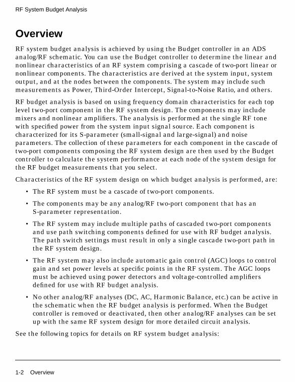
OverviewRF system budget analysis is achieved by using the Budget controller in an ADSanalog/RF schematic. You can use the Budget controller to determine the linear andnonlinear characteristics of an RF system comprising a cascade of two-port linear ornonlinear components. The characteristics are derived at the system input, systemoutput, and at the nodes between the components. The system may include suchmeasurements as Power, Third-Order Intercept, Signal-to-Noise Ratio, and others.
RF budget analysis is based on using frequency domain characteristics for each toplevel two-port component in the RF system design. The components may includemixers and nonlinear amplifiers. The analysis is performed at the single RF tonewith specified power from the system input signal source. Each component ischaracterized for its S-parameter (small-signal and large-signal) and noiseparameters. The collection of these parameters for each component in the cascade oftwo-port components composing the RF system design are then used by the Budgetcontroller to calculate the system performance at each node of the system design forthe RF budget measurements that you select.
Characteristics of the RF system design on which budget analysis is performed, are:
• The RF system must be a cascade of two-port components.
• The components may be any analog/RF two-port component that has anS-parameter representation.
• The RF system may include multiple paths of cascaded two-port componentsand use path switching components defined for use with RF budget analysis.The path switch settings must result in only a single cascade two-port path inthe RF system design.
• The RF system may also include automatic gain control (AGC) loops to controlgain and set power levels at specific points in the RF system. The AGC loopsmust be achieved using power detectors and voltage-controlled amplifiersdefined for use with RF budget analysis.
• No other analog/RF analyses (DC, AC, Harmonic Balance, etc.) can be active inthe schematic when the RF budget analysis is performed. When the Budgetcontroller is removed or deactivated, then other analog/RF analyses can be setup with the same RF system design for more detailed circuit analysis.
See the following topics for details on RF system budget analysis:
1-2 Overview
• “Using the Budget Controller” on page 1-6 describes when you might use theBudget controller, its benefits, how to begin using it, and the location of anexample project.
• “Performing Budget Simulations” on page 1-9 describes application-focusedexamples including
• “A Simple Budget Design” on page 1-10
• “Using Mixers and Multiple Paths” on page 1-12
• “Using Two-Port S-Parameter Files” on page 1-13
• “Using AGC Control Loops” on page 1-14
• “Using Budget with Sweep” on page 1-16
• “Using Budget with Optimization and Yield” on page 1-17
• “Working with Results” on page 1-20 describes how to use the Data Display toview results, and how to export results for post-processing.
• “Reference Measurements and Models” on page 1-32 describes measurementsused for component inputs and outputs, noise figure, and system performance,in addition to various component models.
• “Limitations” on page 1-54 describes the limitations of this frequency domainapproach.
• “Parameters” on page 1-56 describes details of the dialog box fields andparameters for the Budget controller.
• “Theory of Operation” on page 1-60 describes the budget analysis process.
• “Troubleshooting” on page 1-78 explains how to recover from analysis problems.
• “References” on page 1-80 lists information sources that discuss this approachto budget analysis.
Overview 1-3

RF System Budget Analysis
Comparison with the Generic Budget Analysis Functions
In addition to using the Budget controller in ADS analog/RF schematics, ADS alsooffers built-in RF budget MeasEqn function capability. Here are points that comparethese two budget analysis approaches:
• Using the Budget controller is in addition to and does not replace the built-inRF budget MeasEqn function capability.
• The Budget controller is separate from and does not rely on the built-in budgetMeasEqn function items.
The key advantages of the Budget controller over budget analysis functions are:
• Much easier to use.
• Provides many more built-in budget measurements that you can select.
• Provides improved budget noise measurements.
• Supports tuning, sweeps, optimization, yield, etc.
• Supports AGC loops.
• Supports selection between alternate budget paths.
• Supports export of results in ASCII files for use in 3rd-party tools, includingExcel.
The advantages of built-in RF budget MeasEqn function capability are:
• Supports flexible circuit topologies.
• Supports more flexible path selection.
• Supports user-defined subnetworks with frequency conversion.
• Supports more general mixer models.
• Supports concurrent simulation with other analog/RF analyses.
1-4 Overview

The key Budget controller restrictions are:
• For use primarily with cascaded two-port RF systems, though it will alsosupport these multi-pin components:
• S2P
• AGC_Amp
• AGC_PwrControl (for setting up AGC control loops)
• PathSelect2 (for setting up selectable RF paths)
• Input source must be either P_1Tone or P_nTone and requires Z=50 ohms.
• Output load must be either Term or R and requires Z(R)=50 ohms; with nonoise.
• Allows use of only one mixer model: MixerWithLO.
• User-defined circuit subnetworks must be two-port networks and no frequencyconversion is presumed.
• Does not allow concurrent simulation with other analog/RF analyses.
Overview 1-5
RF System Budget Analysis
Using the Budget ControllerThis section will help you decide when to use the Budget controller, and introducesthe basic requirements of an RF system design.
License Requirements
The Budget controller will use the Harmonic Balance simulation license(sim_harmonic) or the RF System simulation license (sim_syslinear). You must haveone of these licenses to run simulations using the Budget controller. You can workwith the examples described in “Performing Budget Simulations” on page 1-9 withoutthe license, but you will not be able to simulate them.
When to Use RF Budget Analysis
Use the Budget controller to perform budget analysis on an RF system. This RFsystem budget analysis provides a simple and easy-to-use capability to determine thelinear and nonlinear characteristics of an RF system comprising a cascade of two-portlinear or nonlinear components. Each component in the RF system chain must havean S-parameter representation.
Using the Budget controller provides you with the following benefits:
• Easily accessible user interface to set up your budget analysis.
• Provides a large number of built-in budget measurements that you can select.
• Provides improved budget noise measurements.
• Enables you to modify your simulation by using tuning, parameter sweeps,optimization, yield analysis, etc.
• Enables you to include AGC loops in your design to control gain and set powerlevels at specific points in the RF system.
• Enables you to select between alternate budget paths.
• Export results in ASCII files for use in third-party tools, including MicrosoftExcel.
1-6 Using the Budget Controller

How to Use the Budget Controller
To use the Budget controller, start by creating an RF system design containingcascaded two-port components. For a successful analysis, be sure your design followsthese requirements:
• Apply ports to the input and output of the two-port cascaded network. Useeither P_1Tone or P_nTone power sources to drive the input. Terminate the endof the cascaded network using port-impedance terminations (Term or R). Verifyimpedance is set to 50 ohms.
• Do not use any components with three or more ports in your design except forS2P, AGC_Amp, AGC_PwrControl, and PathSelect2.
• Use only the MixerWithLO component to define mixers in the RF system. Usingany other mixer component, such as Mixer2, with the Budget controller willresult in the frequency conversion of the mixer being ignored during simulation.
• Add the Budget component to the design from the Simulation-Budget palette orlibrary. Double-click the controller to open its setup dialog box. Click Help fromthe dialog box for descriptions about each field.
• On the Setup tab, you may choose to enable Auto format display withoverwrite. This causes the controller to send a request to the Data Display toautomatically display the simulation results in tables and plots at the end ofthe simulation.
• On the Measurements tab, select the cascaded measurements required to beevaluated. You may choose to not select any cascaded measurements, inwhich case only the system summary results will be evaluated.
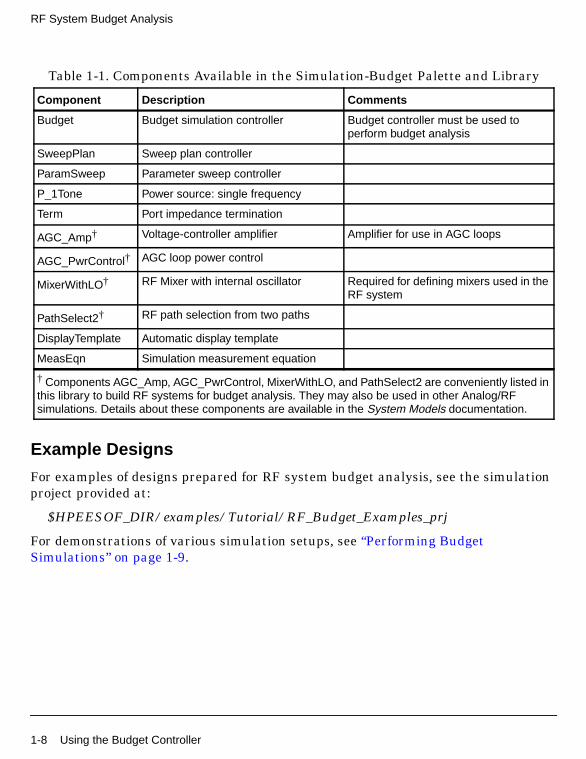
Table 1-1 lists the components located on the Simulation-Budget palette and librarythat are commonly used for budget simulations and sweeps.
Using the Budget Controller 1-7
RF System Budget Analysis
Example Designs
For examples of designs prepared for RF system budget analysis, see the simulationproject provided at:
$HPEESOF_DIR/examples/Tutorial/RF_Budget_Examples_prj
For demonstrations of various simulation setups, see “Performing BudgetSimulations” on page 1-9.
Table 1-1. Components Available in the Simulation-Budget Palette and Library
Component Description Comments
Budget Budget simulation controller Budget controller must be used toperform budget analysis
SweepPlan Sweep plan controller
ParamSweep Parameter sweep controller
P_1Tone Power source: single frequency
Term Port impedance termination
AGC_Amp† Voltage-controller amplifier Amplifier for use in AGC loops
AGC_PwrControl† AGC loop power control
MixerWithLO† RF Mixer with internal oscillator Required for defining mixers used in theRF system
PathSelect2† RF path selection from two paths
DisplayTemplate Automatic display template
MeasEqn Simulation measurement equation
† Components AGC_Amp, AGC_PwrControl, MixerWithLO, and PathSelect2 are conveniently listed inthis library to build RF systems for budget analysis. They may also be used in other Analog/RFsimulations. Details about these components are available in the System Models documentation.
1-8 Using the Budget Controller

Performing Budget SimulationsThis section describes the following example designs included with ADS and how touse the Budget controller with them to perform budget simulations:
• “A Simple Budget Design” on page 1-10 performs a basic budget simulation of atwo-port cascaded network.
• “Using Mixers and Multiple Paths” on page 1-12 performs a budget simulationof a two-port cascaded network containing a mixer component.
• “Using Two-Port S-Parameter Files” on page 1-13 describes the specialconditions about using the S2P component in a cascaded two-port design.
• “Using AGC Control Loops” on page 1-14 performs a basic budget simulation ofa two-port cascaded network containing an AGC loop.
• “Using Budget with Sweep” on page 1-16 performs a budget simulation of atwo-port cascaded network containing a Parameter Sweep controller.
• “Using Budget with Optimization and Yield” on page 1-17 performs a budgetsimulation of a two-port cascaded network containing an Optimizationcontroller.
For detailed descriptions of the Budget controller parameters, see “Parameters” onpage 1-56. For information on the use of the Data Display in the context of budgetsimulations, see “Working with Results” on page 1-20.
Performing Budget Simulations 1-9
RF System Budget Analysis
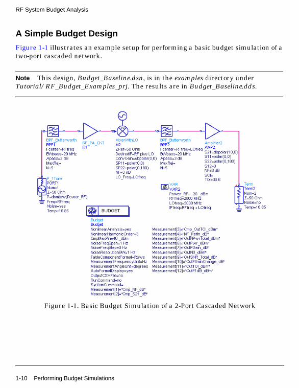
A Simple Budget Design
Figure 1-1 illustrates an example setup for performing a basic budget simulation of atwo-port cascaded network.
Note This design, Budget_Baseline.dsn, is in the examples directory underTutorial/RF_Budget_Examples_prj. The results are in Budget_Baseline.dds.
Figure 1-1. Basic Budget Simulation of a 2-Port Cascaded Network
1-10 Performing Budget Simulations

This design shows a typical RF system design used with budget analysis. It uses aP_1Tone as the source, Term to terminate the cascaded network, and contains a filter,a nonlinear amplifier, a mixer, a second filter, and a second nonlinear amplifierconnected in a chain. The measurements selected in this design are typical onesincluding measurements for component performance, noise, power, and interceptpoints.
Performing Budget Simulations 1-11
RF System Budget Analysis
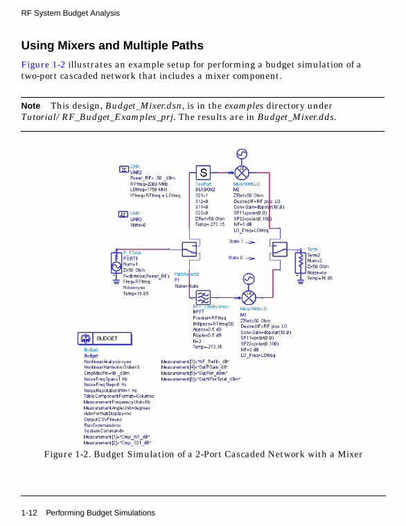
Using Mixers and Multiple Paths
Figure 1-2 illustrates an example setup for performing a budget simulation of atwo-port cascaded network that includes a mixer component.
Note This design, Budget_Mixer.dsn, is in the examples directory underTutorial/RF_Budget_Examples_prj. The results are in Budget_Mixer.dds.
Figure 1-2. Budget Simulation of a 2-Port Cascaded Network with a Mixer
1-12 Performing Budget Simulations
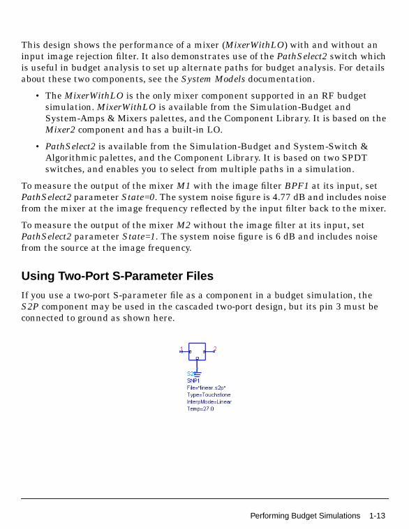
This design shows the performance of a mixer (MixerWithLO) with and without aninput image rejection filter. It also demonstrates use of the PathSelect2 switch whichis useful in budget analysis to set up alternate paths for budget analysis. For detailsabout these two components, see the System Models documentation.
• The MixerWithLO is the only mixer component supported in an RF budgetsimulation. MixerWithLO is available from the Simulation-Budget andSystem-Amps & Mixers palettes, and the Component Library. It is based on theMixer2 component and has a built-in LO.
• PathSelect2 is available from the Simulation-Budget and System-Switch &Algorithmic palettes, and the Component Library. It is based on two SPDTswitches, and enables you to select from multiple paths in a simulation.
To measure the output of the mixer M1 with the image filter BPF1 at its input, setPathSelect2 parameter State=0. The system noise figure is 4.77 dB and includes noisefrom the mixer at the image frequency reflected by the input filter back to the mixer.
To measure the output of the mixer M2 without the image filter at its input, setPathSelect2 parameter State=1. The system noise figure is 6 dB and includes noisefrom the source at the image frequency.
Using Two-Port S-Parameter Files
If you use a two-port S-parameter file as a component in a budget simulation, theS2P component may be used in the cascaded two-port design, but its pin 3 must beconnected to ground as shown here.
Performing Budget Simulations 1-13

RF System Budget Analysis
Using AGC Control Loops
Figure 1-3 illustrates an example setup for performing a basic budget simulation of atwo-port cascaded network that contains an AGC loop.
Note This design, Budget_AGC_Pilot.dsn, is in the examples directory underTutorial/RF_Budget_Examples_prj. The results are in Budget_AGC_Pilot.dds.
Figure 1-3. Typical RF System Design Containing an AGC Loop
This design shows a typical RF system design containing an AGC loop used withbudget analysis. The AGC loop is controlled by the AGC_Amp and AGC_PwrControlcomponents. For details about these two components, see the System Modelsdocumentation.
• AGC_Amp and AGC_PwrControl are the only components supported in an RFbudget simulation for defining AGC loops. They are available from theSimulation-Budget and System-Amps & Mixers palettes, and the ComponentLibrary.
1-14 Performing Budget Simulations

This example uses a Signal tone and an AGC Pilot tone. The AGC Pilot tone controlsthe AGC loop. The Signal tone is defined in the P_nTone source by Freq[1]=RFfreqand P[1]=dbmtow(Power_RF). The Pilot tone is defined in the P_nTone source asFreq[2]=RFpilot and P[2]=dbmtow(Power_Pilot). The AGC_PwrControl component’sTargetPwr parameter is set to 10 dBm. Feedback to the AGC_Amp drives theAGC_Amp within its limits of Min_dB and Max_dB to achieve the TargetPwr level. Inthis example, the AGC_Amp stabilizes to the required Pilot tone gain of 10 dB toachieve the TargetPwr level of 10 dBm for the Pilot tone. This also results in anoutput power for the Signal tone at 0 dBm.
Performing Budget Simulations 1-15
RF System Budget Analysis
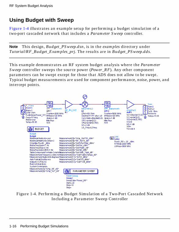
Using Budget with Sweep
Figure 1-4 illustrates an example setup for performing a budget simulation of atwo-port cascaded network that includes a Parameter Sweep controller.
Note This design, Budget_PSweep.dsn, is in the examples directory underTutorial/RF_Budget_Examples_prj. The results are in Budget_PSweep.dds.
This example demonstrates an RF system budget analysis where the ParameterSweep controller sweeps the source power (Power_RF). Any other componentparameters can be swept except for those that ADS does not allow to be swept.Typical budget measurements are used for component performance, noise, power, andintercept points.
Figure 1-4. Performing a Budget Simulation of a Two-Port Cascaded NetworkIncluding a Parameter Sweep Controller
1-16 Performing Budget Simulations

Using Budget with Optimization and Yield
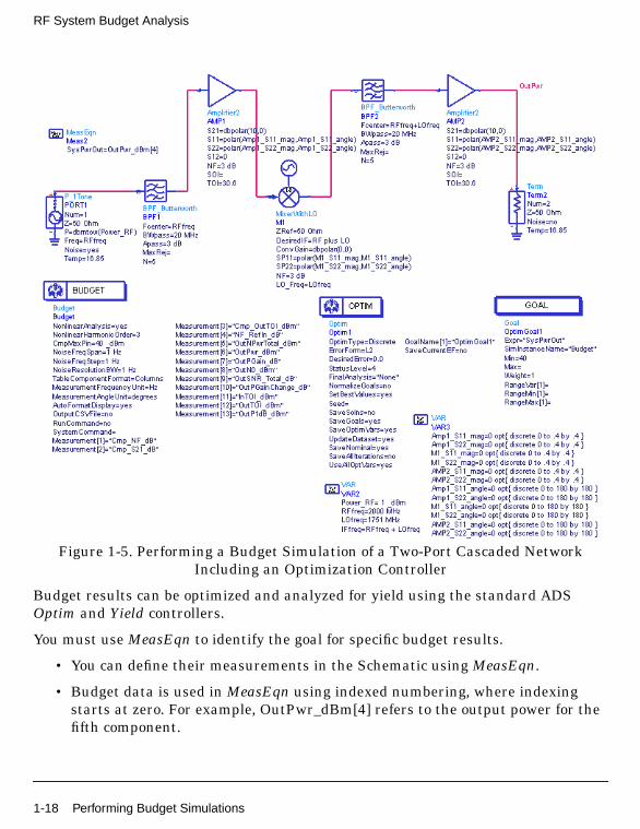
Figure 1-5 illustrates an example setup for performing a budget simulation of atwo-port cascaded network that includes an Optimization controller.
Note This design, Budget_MinMax_Reflection.dsn, is in the examples directoryunder Tutorial/RF_Budget_Examples_prj. The results are inBudget_MinMax_Reflection.dds.
This design demonstrates the use of a Budget controller with statistical analysis formin/max reflection performance.
Performing Budget Simulations 1-17
RF System Budget Analysis
Figure 1-5. Performing a Budget Simulation of a Two-Port Cascaded NetworkIncluding an Optimization Controller
Budget results can be optimized and analyzed for yield using the standard ADSOptim and Yield controllers.
You must use MeasEqn to identify the goal for specific budget results.
• You can define their measurements in the Schematic using MeasEqn.
• Budget data is used in MeasEqn using indexed numbering, where indexingstarts at zero. For example, OutPwr_dBm[4] refers to the output power for thefifth component.
1-18 Performing Budget Simulations

• SysPwrOut can be used for optimization, yield, etc. as shown in the example inFigure 1-5.
For a complete listing of names for all available Budget measurements, see the tablesin “RF Budget Cascade Measurements” on page 1-32 and “RF Budget SummaryMeasurements” on page 1-39. These tables show the short names for the Budgetmeasurements. The long name for a Budget measurement is defined as:
<schematic_design_name>.Budget.<measurement_name>
When setting up RF Budget Summary Measurements to use for optimization:
• The independent variable is Index.
• The name to be used in the MeasEqn is Summary_Value[x], where x is theIndex for the Summary Measurement desired.
• For example, the SystemNF_dB system summary measurement has Index=5, sothe MeasEqn should use Summary_Value[5].
When setting up RF Budget Cascade Measurements to use for optimization:
• On the Setup tab, when Components In is set to Columns:
• The independent variable is Cmp_Index.
• The name to be used in the MeasEqn is the actual cascade measurementname associated with the specific component.
• For example, the OutPwr_dBm system cascade measurement for the fourthcomponent should use OutPwr_dBm[3].
• On the Setup tab, when Components In is set to Rows:
• The independent variable is Meas_Index.
• The name to be used in the MeasEqn is the system reference designatorassociated with the specific cascade measurement.
• For example, the fourth measurement for the component with referencedesignator A1 should use A1[3]. If you had defined the fourth measurementto be OutPwr_dBm, then A1[3] means the OutPwr_dBm is associated withthe component whose reference designator is A1.
Performing Budget Simulations 1-19

RF System Budget Analysis
Working with ResultsThis section describes how to work with results from budget simulations:
• “Viewing Results Using the ADS Data Display” on page 1-20 describes how toformat and display results in the Data Display.
• “Exporting and Post-Processing Results” on page 1-26 describes how to exportsimulation results to a text file using the Comma Separated Values (CSV)format.
Viewing Results Using the ADS Data Display
There are different ways to format and display budget simulation results in the DataDisplay:
• Enable the automatic formatting feature in the Budget controller.
• Use an existing Data Display page or template that is custom formatted theway you prefer.
Automatic Formatting
The results from a budget simulation can be formatted and displayed automaticallyin tables and plots preconfigured for the Budget controller. Enabling this featurecauses the Budget controller to send a command to the Data Display window at theend of the budget simulation to format and display the results.
Caution Enabling the automatic formatting feature can overwrite an existingformatted Data Display page. Make sure valuable data is not overwritten and lost.
To enable automatic formatting:
• In the Budget controller’s setup dialog box, select the option Auto format displaywith overwrite on the Setup tab in the Results section.
• On the schematic, set the parameter AutoFormatDisplay=Yes .
In addition to enabling the automatic formatting feature, you must be sure to set upthe simulation so a default Data Display window opens at the end of the simulation.In the Schematic window, choose Simulate > Simulation Setup, then select the option
1-20 Working with Results
Open Data Display when simulation completes. For more information about settingup simulations, see chapter 1 in Using Circuit Simulators.
If you are not familiar with setting up formatting in the Data Display, Agilent EEsofrecommends that you enable the automatic formatting option the first time you run abudget simulation to help you learn how to display results. However, use this featurecarefully to avoid accidently overwriting existing results. When you are comfortablewith the Data Display and its formatting features, disable the automatic formatting.
Note If automatic formatting is disabled, the simulation results are still written tothe dataset, but they are not automatically formatted and displayed in the DataDisplay. This can be useful when you have a custom formatted Data Display page ortemplate that you prefer for displaying simulation results.
With the correct setup and after a successful simulation, a Data Display window willopen at the end of the simulation containing three pages, which are discussed in thefollowing sections:
• “Summary tables” on page 1-22
• “Measurement tables” on page 1-23
• “Measurement plots” on page 1-25
Note If no measurements are selected for a budget simulation, the Measurementtables and Measurement plots pages are not created since no measurement resultsare evaluated. The Summary tables page is displayed by default.
Working with Results 1-21

RF System Budget Analysis
Summary tables
The Summary tables page displays a table with the summary measurements andsystem measurements for the design being simulated. The results are formatted asshown in the example shown in Figure 1-6. All of the summary measurements areevaluated and written to the dataset for every budget simulation, so they are notavailable for individual selection on the Budget controller’s Measurement tab. Forinformation on the individual measurements, see “RF Budget SummaryMeasurements” on page 1-39.
Figure 1-6. Summary Tables for a Budget Simulation
1-22 Working with Results
Measurement tables
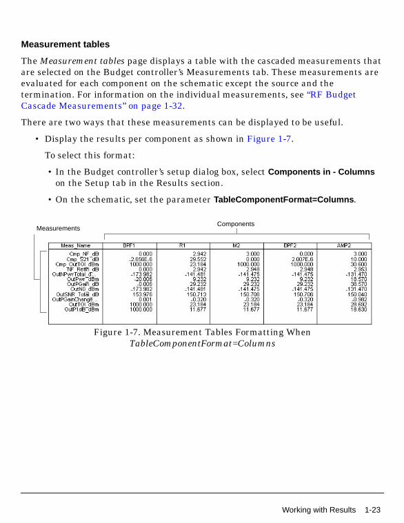
The Measurement tables page displays a table with the cascaded measurements thatare selected on the Budget controller’s Measurements tab. These measurements areevaluated for each component on the schematic except the source and thetermination. For information on the individual measurements, see “RF BudgetCascade Measurements” on page 1-32.
There are two ways that these measurements can be displayed to be useful.
• Display the results per component as shown in Figure 1-7.
To select this format:
• In the Budget controller’s setup dialog box, select Components in - Columnson the Setup tab in the Results section.
• On the schematic, set the parameter TableComponentFormat=Columns .
Figure 1-7. Measurement Tables Formatting WhenTableComponentFormat=Columns
ComponentsMeasurements
Working with Results 1-23
RF System Budget Analysis
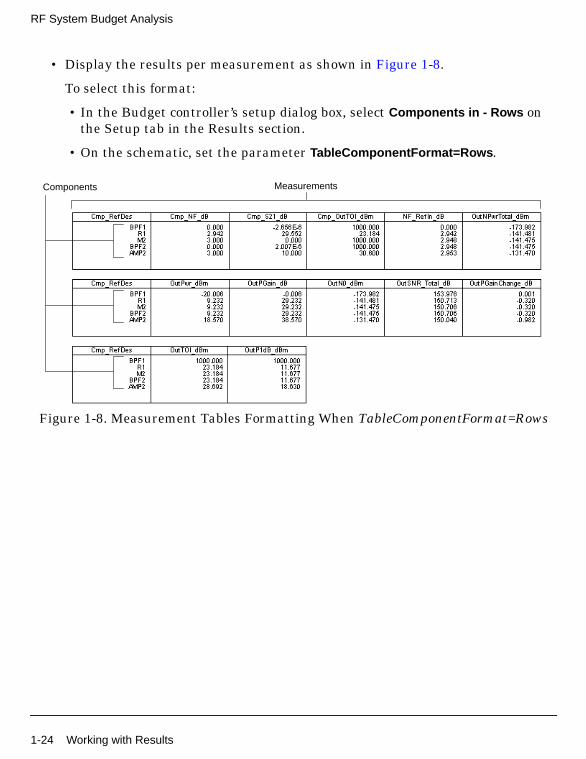
• Display the results per measurement as shown in Figure 1-8.
To select this format:
• In the Budget controller’s setup dialog box, select Components in - Rows onthe Setup tab in the Results section.
• On the schematic, set the parameter TableComponentFormat=Rows .
Figure 1-8. Measurement Tables Formatting When TableComponentFormat=Rows
MeasurementsComponents
1-24 Working with Results

Measurement plots
The Measurement plots page displays the same data as the Measurement tables page,but formatted in stacked plots instead of tables. The plots are stacked in groups ofthree plots per column, and the X-axis in each plot is the component index.Component indexing starts from 0. For example, in a design where the fifthcomponent after the source is AMP1, the index for this component is 4 in each plot.
MeasurementsComponent Indexes
Working with Results 1-25
RF System Budget Analysis
Custom Formatting
If you have an existing Data Display page or template that is formatted the way youprefer, then disable the automatic format display feature. When the simulationfinishes, a default Data Display page or template is opened if selected.
To disable automatic formatting:
• In the Budget controller’s setup dialog box, deselect (uncheck) the option Autoformat display with overwrite on the Setup tab in the Results section.
• On the schematic, set the parameter AutoFormatDisplay=No .
Make sure that the Simulation Setup is configured such that a default Data Displaywindow is opened at the end of the simulation (in the Schematic window, chooseSimulate > Simulation Setup).
Exporting and Post-Processing Results
The results from a budget simulation can be exported to a text file, in the CommaSeparated Values (CSV) format. This can be useful if you are familiar with usingspreadsheet applications for budget analysis such as Microsoft Excel.
To enable exporting results to a CSV file:
• In the Budget controller’s setup dialog box, enable the option Output results ascomma separated values (CSV) to file on the Setup tab in the Results section.
• On the schematic, set the parameter OutputCSVFile=Yes .
When this feature is enabled, the simulation results are written to the data directoryof the current ADS project, into a text file named <design_name>.csv, where<design_name> is the name of the ADS schematic design being simulated. Theresults written to the CSV file include:
• System summary measurements data
• Cascade measurements data
The Budget controller also provides a facility for post-processing the CSV file at theend of the simulation. It enables you to run a command to reformat the CSV file intoa format that’s easier to use.
1-26 Working with Results
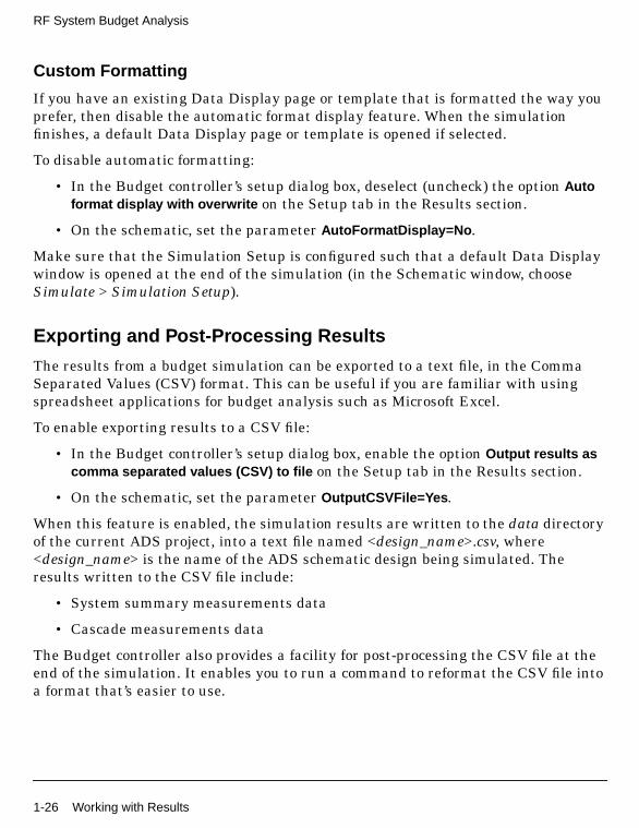
To enable the post-processing facility:
• In the Budget controller’s setup dialog box, enable the option Run commandafter analysis on the Setup tab in the Results section. Then, enter the commandthat post-processes the CSV file in the entry field for System command . Here isan example of a command that you can enter:
C:\Program Files\Microsoft Office\Office\Excel.exe
• On the schematic, set the parameter RunCommand=Yes , and enter thecommand that post-processes the CSV file for the SystemCommand parameter.Here is an example of a command you can enter (including quotation marks):
SystemCommand=“C:\Program Files\Microsoft Office\Office\Excel.exe”
Figure 1-9 shows an example of how the setup dialog is prepared to output a CSV fileand post-process the file.
Figure 1-9. Setup Tab Set for Post-Processing CSV File
Here are additional details about using the post-processing command:
• You can define a command on any supported platform. When specifying anexecutable or shell script, use either its full path or a path relative to the datadirectory of the currently open ADS project.
• A typical use on a Windows PC is to run Excel at the end of the simulation toopen the CSV file. A typical use on UNIX or Linux platforms is to run a scriptwritten in a scripting language to reformat the CSV file into a format that’seasier to use.
• The system command specified in the Budget controller is executed at the endof the simulation.
Output results asCSV file and runcommand
Working with Results 1-27

RF System Budget Analysis
• The Budget controller automatically appends the name of the CSV file to thecommand string. For example, if the command string isC:\Program Files\Microsoft Office\Office\Excel.exe
then the actual command executed isC:\Program Files\Microsoft Office\Office\Excel.exe <design_name>.cs v
Example Excel Spreadsheet
ADS includes an example of a user-defined Excel spreadsheet. It contains a macrothat you can use to post-process an exported CSV file. This Excel macro will processthe CSV file into formatted tables and plots for each measurement. The spreadsheetis named SetUp_Budget_Sheets.xls and it is located in$HPEESOF_DIR/examples/Tutorial/RF_Budget_Examples_prj. The followingfigure shows SetUp_Budget_Sheets.xls opened to the Icons worksheet.
Important Agilent EEsof EDA will not provide any support for this spreadsheet.This Excel spreadsheet is provided on an as-is basis to illustrate use of a user-definedmacro to post-process exported results from a budget simulation. This samplespreadsheet has been tested only with Microsoft Excel 2000, version 9.0.7616 SP3. Ithas been found that the system command and/or spreadsheet macro fail to executewith earlier versions of Microsoft Excel.
1-28 Working with Results

Working with Results 1-29

RF System Budget Analysis
To use the sample spreadsheet:
1. Copy the file SetUp_Budget_Sheets.xls from the folder$HPEESOF_DIR/examples/Tutorial/RF_Budget_Examples_prj.
2. Paste the .xls file into the Office\XLStart folder. For example, if the Excel.exeexecutable’s location isC:\Program Files\Microsoft Office\Office\Excel.exethen the XLStart folder is atC:\Program Files\Microsoft Office\Office\XLStart.
Note Any Microsoft Excel spreadsheet in the Office\XLStart folder will beopened any time Microsoft Excel is launched, even independent of ADS. Toavoid this, Agilent EEsof EDA recommends that you delete the fileSetUp_Budget_Sheets.xls from the Office\XLStart folder after yourrequirement to use it for budget analysis is complete.
3. When the Budget controller launches Excel at the end of the simulation, itopens the CSV file containing the simulation data. When the CSV file opens inExcel, the macro is available in the background.
Run the macro using the keyboard shortcut Ctrl-R . The following figure showsthe CSV file after running the macro, opened to the Cascade_Meas worksheet.Additional worksheets are available named after each measurement, andcontaining a plot of the data for that measurement.
1-30 Working with Results
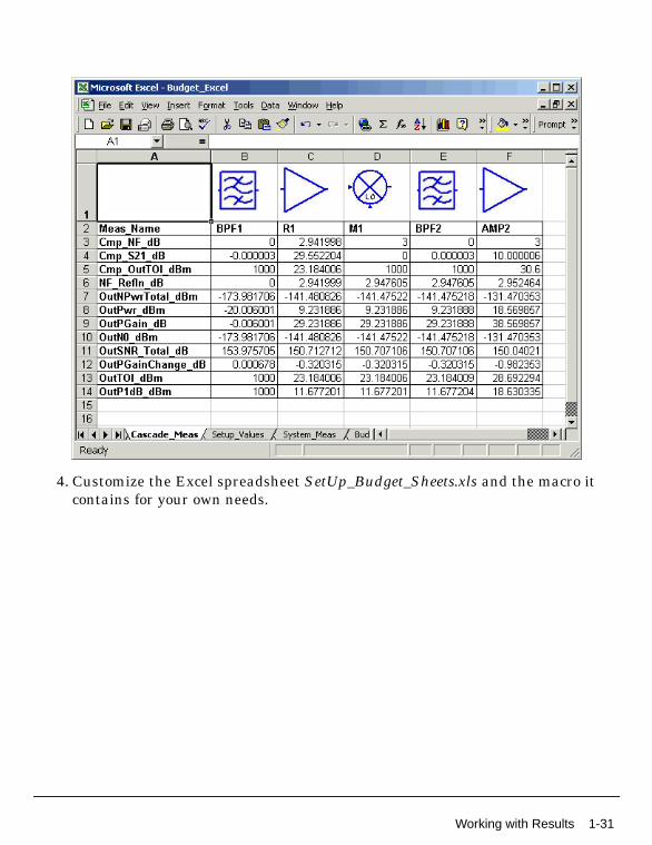
4. Customize the Excel spreadsheet SetUp_Budget_Sheets.xls and the macro itcontains for your own needs.
Working with Results 1-31

RF System Budget Analysis
Reference Measurements and ModelsThis section provides the details about the measurements and component modelsused by the Budget controller:
• “RF Budget Cascade Measurements” on page 1-32
• “RF Budget Summary Measurements” on page 1-39
• “RF Budget Analysis Component Models” on page 1-41
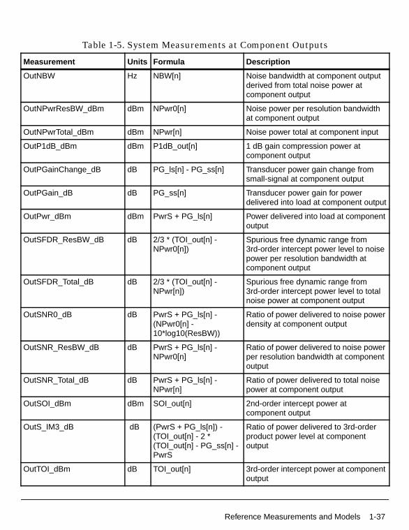
RF Budget Cascade Measurements
You can select Budget Cascade Measurements of interest from the Budget controller’sMeasurements tab. These measurements produce a measurement value at eachsystem node. For example, a system with five components will produce five values foreach cascade measurement. These measurements are grouped as follows, and aredescribed in the following sections:
• “Component Measurements” on page 1-33
• “Noise Figure Measurements” on page 1-34
• “System Measurements at Component Inputs” on page 1-35
• “System Measurements at Component Outputs” on page 1-36
1-32 Reference Measurements and Models
Component Measurements
The formulas in Table 1-2 reference the raw data defined in “Raw Data Generated foran RF Budget Analysis” on page 1-69.
Table 1-2. Component Measurements
Measurement Units Formula Description
Cmp_Ctrb_SysNF_NoImage_dB dB Cmp_Ctrb_SysNF_NoImage[n]
System noise figure improvementif component contributes nonoise; excludes system imagenoise
Cmp_Ctrb_SysTOI_dB dB Cmp_Ctrb_SysTOI[n] System output 3rd-order interceptimprovement if component islinear
Cmp_LS_GainChange_dB dB (G_ss[n] - PG_ss[n-1]) -(PG_ls[n] - PG_ls[n-1])
Difference between componenteffective small-signal gain andlarge-signal gain within system
Cmp_NF_dB dB Cmp_NF[n] Component noise figure
Cmp_OutN0_dBm dBm 30 +10.*log10(k*290*ResBW)+ Cmp_NF[n] +Cmp_S21[n,0]
Component output noise density
Cmp_OutP1dB_dBm dBm Cmp_OutP1[n] Component output 1 dB gaincompression power level
Cmp_OutSOI_dBm dBm Cmp_OutSOI[n] Component output 2nd-orderintercept
Cmp_OutTOI_dBm dBm Cmp_OutTOI[n] Component output 3rd-orderintercept
Cmp_S11_dB dB Cmp_S11[n, 0] Component 50 ohm S11 in dB
Cmp_S11_mag dB Cmp_S11[n, 1] Component 50 ohm S11magnitude
Cmp_S11_phase dB Cmp_S11[n, 2] Component 50 ohm S11 phase
Cmp_S12_dB dB Cmp_S12[n, 0] Component 50 ohm S12 in dB
Cmp_S12_mag dB Cmp_S12[n, 1] Component 50 ohm S12magnitude
Cmp_S12_phase dB Cmp_S12[n, 2] Component 50 ohm S12 phase
Cmp_S21_dB dB Cmp_S21[n, 0] Component 50 ohm S21 in dB
Reference Measurements and Models 1-33

RF System Budget Analysis
Noise Figure Measurements
The formulas in Table 1-3 reference the raw data defined in “Raw Data Generated foran RF Budget Analysis” on page 1-69.
Cmp_S21_mag dB Cmp_S21[n, 1] Component 50 ohm S21magnitude
Cmp_S21_phase dB Cmp_S21[n, 2] Component 50 ohm S21 phase
Cmp_S22_dB dB Cmp_S22[n, 0] Component 50 ohm S22 in dB
Cmp_S22_mag dB Cmp_S22[n, 1] Component 50 ohm S22magnitude
Cmp_S22_phase dB Cmp_S22[n, 2] Component 50 ohm S22 phase
Cmp_SS_MismatchLoss_dB dB Cmp_S21[n,0] -(PG_ss[n] - PG_ss[n-1])
Difference between component50 ohm small-signal gain andeffective small-signal gain withinsystem
Cmp_SS_PGain_dB dB PG_ss[n] - PG_ss[n-1] Component effective small-signalgain within system
Table 1-3. Noise Figure Measurements
Measurement Units Formula Description
NF_RefIn_NoImage_dB dB NF_refin_no_image[n] Noise figure from system input tocomponent output with image noiseexcluded
NF_RefIn_dB dB NF_refin[n] Noise figure from system input tocomponent output
NF_RefOut_NoImage_dB dB NF_refout_no_image[n] Noise figure from component input tosystem output with image noiseexcluded
NFactor_RefIn_dB dB 10^(NF_refin[n]/10) Noise factor from system input tocomponent output
Table 1-2. Component Measurements
Measurement Units Formula Description
1-34 Reference Measurements and Models
System Measurements at Component Inputs
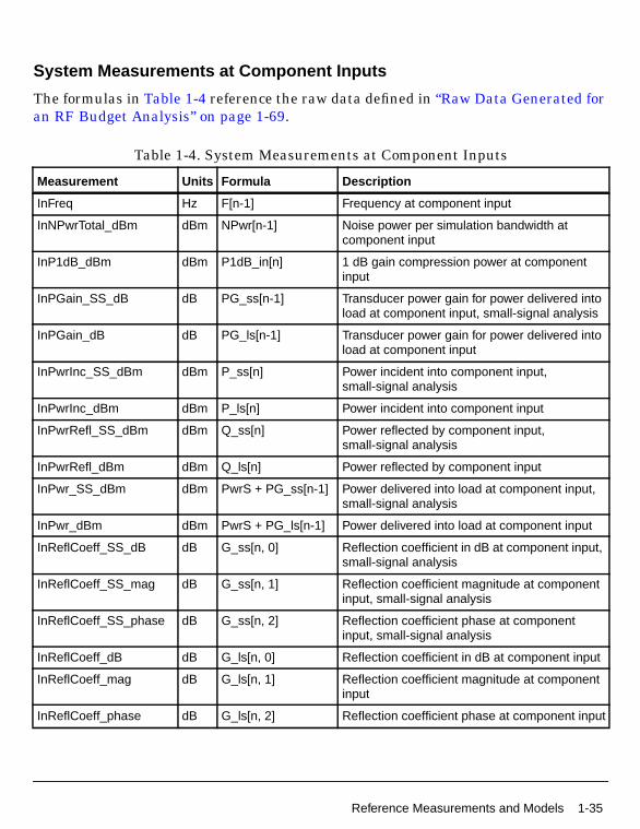
The formulas in Table 1-4 reference the raw data defined in “Raw Data Generated foran RF Budget Analysis” on page 1-69.
Table 1-4. System Measurements at Component Inputs
Measurement Units Formula Description
InFreq Hz F[n-1] Frequency at component input
InNPwrTotal_dBm dBm NPwr[n-1] Noise power per simulation bandwidth atcomponent input
InP1dB_dBm dBm P1dB_in[n] 1 dB gain compression power at componentinput
InPGain_SS_dB dB PG_ss[n-1] Transducer power gain for power delivered intoload at component input, small-signal analysis
InPGain_dB dB PG_ls[n-1] Transducer power gain for power delivered intoload at component input
InPwrInc_SS_dBm dBm P_ss[n] Power incident into component input,small-signal analysis
InPwrInc_dBm dBm P_ls[n] Power incident into component input
InPwrRefl_SS_dBm dBm Q_ss[n] Power reflected by component input,small-signal analysis
InPwrRefl_dBm dBm Q_ls[n] Power reflected by component input
InPwr_SS_dBm dBm PwrS + PG_ss[n-1] Power delivered into load at component input,small-signal analysis
InPwr_dBm dBm PwrS + PG_ls[n-1] Power delivered into load at component input
InReflCoeff_SS_dB dB G_ss[n, 0] Reflection coefficient in dB at component input,small-signal analysis
InReflCoeff_SS_mag dB G_ss[n, 1] Reflection coefficient magnitude at componentinput, small-signal analysis
InReflCoeff_SS_phase dB G_ss[n, 2] Reflection coefficient phase at componentinput, small-signal analysis
InReflCoeff_dB dB G_ls[n, 0] Reflection coefficient in dB at component input
InReflCoeff_mag dB G_ls[n, 1] Reflection coefficient magnitude at componentinput
InReflCoeff_phase dB G_ls[n, 2] Reflection coefficient phase at component input
Reference Measurements and Models 1-35
RF System Budget Analysis
System Measurements at Component Outputs
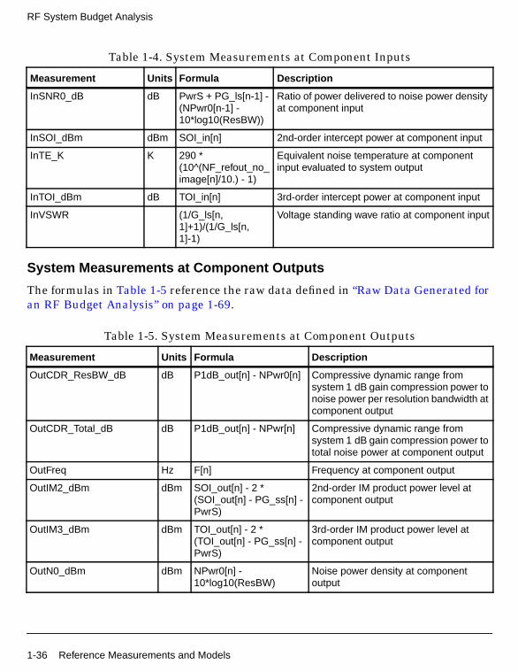
The formulas in Table 1-5 reference the raw data defined in “Raw Data Generated foran RF Budget Analysis” on page 1-69.
InSNR0_dB dB PwrS + PG_ls[n-1] -(NPwr0[n-1] -10*log10(ResBW))
Ratio of power delivered to noise power densityat component input
InSOI_dBm dBm SOI_in[n] 2nd-order intercept power at component input
InTE_K K 290 *(10^(NF_refout_no_image[n]/10.) - 1)
Equivalent noise temperature at componentinput evaluated to system output
InTOI_dBm dB TOI_in[n] 3rd-order intercept power at component input
InVSWR (1/G_ls[n,1]+1)/(1/G_ls[n,1]-1)
Voltage standing wave ratio at component input
Table 1-5. System Measurements at Component Outputs
Measurement Units Formula Description
OutCDR_ResBW_dB dB P1dB_out[n] - NPwr0[n] Compressive dynamic range fromsystem 1 dB gain compression power tonoise power per resolution bandwidth atcomponent output
OutCDR_Total_dB dB P1dB_out[n] - NPwr[n] Compressive dynamic range fromsystem 1 dB gain compression power tototal noise power at component output
OutFreq Hz F[n] Frequency at component output
OutIM2_dBm dBm SOI_out[n] - 2 *(SOI_out[n] - PG_ss[n] -PwrS)
2nd-order IM product power level atcomponent output
OutIM3_dBm dBm TOI_out[n] - 2 *(TOI_out[n] - PG_ss[n] -PwrS)
3rd-order IM product power level atcomponent output
OutN0_dBm dBm NPwr0[n] -10*log10(ResBW)
Noise power density at componentoutput
Table 1-4. System Measurements at Component Inputs
Measurement Units Formula Description
1-36 Reference Measurements and Models
OutNBW Hz NBW[n] Noise bandwidth at component outputderived from total noise power atcomponent output
OutNPwrResBW_dBm dBm NPwr0[n] Noise power per resolution bandwidthat component output
OutNPwrTotal_dBm dBm NPwr[n] Noise power total at component input
OutP1dB_dBm dBm P1dB_out[n] 1 dB gain compression power atcomponent output
OutPGainChange_dB dB PG_ls[n] - PG_ss[n] Transducer power gain change fromsmall-signal at component output
OutPGain_dB dB PG_ss[n] Transducer power gain for powerdelivered into load at component output
OutPwr_dBm dBm PwrS + PG_ls[n] Power delivered into load at componentoutput
OutSFDR_ResBW_dB dB 2/3 * (TOI_out[n] -NPwr0[n])
Spurious free dynamic range from3rd-order intercept power level to noisepower per resolution bandwidth atcomponent output
OutSFDR_Total_dB dB 2/3 * (TOI_out[n] -NPwr[n])
Spurious free dynamic range from3rd-order intercept power level to totalnoise power at component output
OutSNR0_dB dB PwrS + PG_ls[n] -(NPwr0[n] -10*log10(ResBW))
Ratio of power delivered to noise powerdensity at component output
OutSNR_ResBW_dB dB PwrS + PG_ls[n] -NPwr0[n]
Ratio of power delivered to noise powerper resolution bandwidth at componentoutput
OutSNR_Total_dB dB PwrS + PG_ls[n] -NPwr[n]
Ratio of power delivered to total noisepower at component output
OutSOI_dBm dBm SOI_out[n] 2nd-order intercept power atcomponent output
OutS_IM3_dB dB (PwrS + PG_ls[n]) -(TOI_out[n] - 2 *(TOI_out[n] - PG_ss[n] -PwrS
Ratio of power delivered to 3rd-orderproduct power level at componentoutput
OutTOI_dBm dB TOI_out[n] 3rd-order intercept power at componentoutput
Table 1-5. System Measurements at Component Outputs
Measurement Units Formula Description
Reference Measurements and Models 1-37

RF System Budget Analysis
OutVGainInc_SS_dB dB VGI_ss[n, 0] Voltage gain in dB for wave incident onload at component output, small-signalanalysis
OutVGainInc_SS_mag dB VGI_ss[n, 1] Voltage gain magnitude for waveincident on load at component output,small-signal analysis
OutVGainInc_SS_phase dB VGI_ss[n, 2] Voltage gain phase for wave incident onload at component output, small-signalanalysis
OutVGainInc_dB dB VGI_ls[n, 0] Voltage gain in dB for wave incident onload at component output
OutVGainInc_mag dB VGI_ls[n, 1] Voltage gain magnitude for waveincident on load at component output
OutVGainInc_phase dB VGI_ls[n, 2] Voltage gain phase for wave incident onload at component output
OutVGainRefl_SS_dB dB VGR_ss[n, 0] Voltage gain in dB for wave reflected byload at component output, small-signalanalysis
OutVGainRefl_SS_mag dB VGR_ss[n, 2] Voltage gain magnitude for wavereflected by load at component output,small-signal analysis
OutVGainRefl_SS_phase dB VGR_ss[n, 1] Voltage gain phase for wave reflectedby load at component output,small-signal analysis
OutVGainRefl_dB dB VGR_ls[n, 0] Voltage gain in dB for wave reflected byload at component output
OutVGainRefl_mag dB VGR_ls[n, 1] Voltage gain magnitude for wavereflected by load at component output
OutVGainRefl_phase dB VGR_ls[n, 2] Voltage gain phase for wave reflectedby load at component output
Table 1-5. System Measurements at Component Outputs
Measurement Units Formula Description
1-38 Reference Measurements and Models
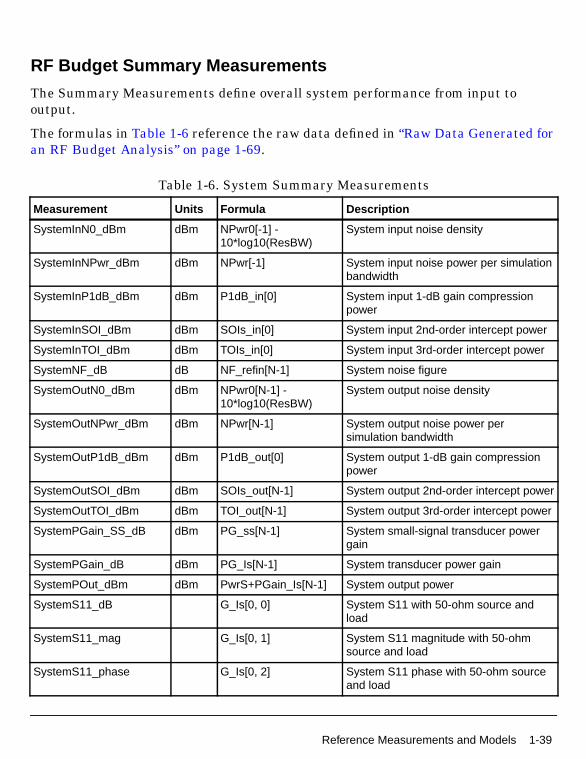
RF Budget Summary Measurements
The Summary Measurements define overall system performance from input tooutput.
The formulas in Table 1-6 reference the raw data defined in “Raw Data Generated foran RF Budget Analysis” on page 1-69.
Table 1-6. System Summary Measurements
Measurement Units Formula Description
SystemInN0_dBm dBm NPwr0[-1] -10*log10(ResBW)
System input noise density
SystemInNPwr_dBm dBm NPwr[-1] System input noise power per simulationbandwidth
SystemInP1dB_dBm dBm P1dB_in[0] System input 1-dB gain compressionpower
SystemInSOI_dBm dBm SOIs_in[0] System input 2nd-order intercept power
SystemInTOI_dBm dBm TOIs_in[0] System input 3rd-order intercept power
SystemNF_dB dB NF_refin[N-1] System noise figure
SystemOutN0_dBm dBm NPwr0[N-1] -10*log10(ResBW)
System output noise density
SystemOutNPwr_dBm dBm NPwr[N-1] System output noise power persimulation bandwidth
SystemOutP1dB_dBm dBm P1dB_out[0] System output 1-dB gain compressionpower
SystemOutSOI_dBm dBm SOIs_out[N-1] System output 2nd-order intercept power
SystemOutTOI_dBm dBm TOI_out[N-1] System output 3rd-order intercept power
SystemPGain_SS_dB dBm PG_ss[N-1] System small-signal transducer powergain
SystemPGain_dB dBm PG_Is[N-1] System transducer power gain
SystemPOut_dBm dBm PwrS+PGain_Is[N-1] System output power
SystemS11_dB G_Is[0, 0] System S11 with 50-ohm source andload
SystemS11_mag G_Is[0, 1] System S11 magnitude with 50-ohmsource and load
SystemS11_phase G_Is[0, 2] System S11 phase with 50-ohm sourceand load
Reference Measurements and Models 1-39

RF System Budget Analysis
SystemS12_dB System_S12[0] System S12 with 50-ohm source andload
SystemS12_mag System_S12[1] System S12 magnitude with 50-ohmsource and load
SystemS12_phase System_S12[2] System S12 phase with 50-ohm sourceand load
SystemS21_dB VGI_Is[N-1, 0] System S21 with 50-ohm source andload
SystemS21_mag VGI_Is[N-1, 1] System S21 magnitude with 50-ohmsource and load
SystemS21_phase VGI_Is[N-1, 2] System S21 phase with 50-ohm sourceand load
SystemS22_dB System_S22[0] System S22 with 50-ohm source andload
SystemS22_mag System_S22[1] System S22 magnitude with 50-ohmsource and load
SystemS22_phase System_S22[2] System S22 phase with 50-ohm sourceand load
System_AnalysisType System_AnalysisType Analysis type (0=linear, 1=nonlinear)
System_NoiseResBW Hz ResBW Noise analysis resolution bandwidth
System_NoiseSimBW Hz SimBW Noise analysis simulation bandwidth
System_NoiseSimFStep Hz SimFStep Noise analysis simulation frequency step
System_PilotFreq Hz FreqPilot System source pilot tone frequency forAGC loops
System_PilotPwr_dBm dBm PwrPilot System source pilot tone power
SystemRefR ohms RefR System reference resistance
System_SourceFreq Hz FreqS System source frequency
System_SourcePwr_dBm dBm PwrS System source power
System_SourceTemp Celsius TempS System source temperature
Table 1-6. System Summary Measurements
Measurement Units Formula Description
1-40 Reference Measurements and Models
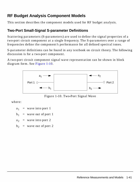
RF Budget Analysis Component Models
This section describes the component models used for RF budget analysis.
Two-Port Small-Signal S-parameter Definitions
Scattering parameters (S-parameters) are used to define the signal properties of atwo-port circuit component at a single frequency. The S-parameters over a range offrequencies define the component’s performance for all defined spectral tones.
S-parameter definitions can be found in any textbook on circuit theory. The followingdiscussion is for a two-port component.
A two-port circuit component signal wave representation can be shown in blockdiagram form. See Figure 1-10.
Figure 1-10. Two-Port Signal Wave
where:
a1 = wave into port 1
b1 = wave out of port 1
a2 = wave into port 2
b2 = wave out of port 2
Port 1 Port 2
a1
b1
a2
b2
Reference Measurements and Models 1-41

RF System Budget Analysis
The S-parameters for this conventional component are defined in standardmicrowave text books as follows:
b1 = a1 s11 + a2 s12
b2 = a1 s21 + a2 s22
where:
S-parameters are defined with respect to a reference impedance that is typically 50ohms. For 50-ohm S-parameters, and with the two-port component terminated with50 ohms at each port, the s21 parameter is simply the voltage gain of the componentfrom port 1 to port 2.
These equations can be solved for b1 and a1 in terms of a2 and b2 to yield thetransmission (T) parameters as follows:
b1 = a2 t11 + b2 t12
a1 = a2 t21 + b2 t22
The T-parameters are related to the S-parameters as follows:
S-parameter Definitions for Components with Spectral Inversions
A spectral inversion (SI) component is a component whose output signal is derivedfrom the conjugate phase of the input signal. This typically occurs for downconverting mixers with an LO frequency greater than the input RF frequency.
The frequency inversion of signals through a spectral inverting component bringsabout a conjugate transformation to the transmitted wave. This transformation
s11 = port 1 reflection coefficient: s11 = b1/a1; a2 = 0
s22 = port 2 reflection coefficient: s22 = b2/a2; a1 = 0
s21 = forward transmission coefficient: s21 = b2/a1; a2 = 0
s12 = reverse transmission coefficient: s12 = b1/a2; a1 = 0
t11 t12
t12 t22
s12 s11s22s21--------–
s11s21--------
s22s21--------–
1s21--------
=
1-42 Reference Measurements and Models
makes use of the property of the mixer which can be modeled as a multiplier of theinput and local oscillator waveforms:
Vin (t) = cos(wi • t + Phi)
VLO (t) = cos(wlo • t); assume wlo > wi
Vo(t) = Vin * VLO
Vo(t) = 0.5 cos((wlo-wi) t - Phi) + 0.5 cos((wlo+wi) t + Phi)
As shown, the lower sideband component, wlo-wi, has a phase component which isthe conjugate of the input phase.
The S-parameter definitions for a spectral inverting component must account for thespectral inversion that occurs at the output. Therefore, the S-parameters for aspectral inverting component are slightly different than those of a conventionalcomponent (see references [10], [11], and [12] in “References” on page 1-80).(* in the following represents conjugate):
s11 is the port 1 reflection coefficient: s11 = b1/a1; a2 = 0
s22 is the port 2 reflection coefficient: s22 = b2/a2; a1 = 0
s21 is the forward transmission coefficient: s21 = b2/a1*; a2 = 0
s12 is the reverse transmission coefficient: s12 = b1/a2*; a1 = 0
Note that s21 and s12 account for the conjugate of the incident wave. The definitionsfor s11 and s12 above are slightly different from the convention used in reference [10]in which s11 = b1*/a1* and s12 = b1*/a2.
The reverse transmission wave, b1, and forward transmission wave, b2, are asfollows:
b1 = a1 s11 + a2* s12b2 = a1* s21 + a2 s22
Two-Port Noise Parameter Definitions
Noise parameters are used to define the noise properties of a circuit component at asingle frequency. The noise parameters over a range of frequencies define thecomponent’s performance for all noise power spectral density spectral tones definingan incident noise.
Reference Measurements and Models 1-43
RF System Budget Analysis
Noise parameter definitions can be found in any textbook on circuit theory. Noisewave parameters are used by the program to define the noise properties of any circuitcomponent. The following discussion is for a two-port component.
The two-port component noise wave representation may use two noise waves at thecomponent input (see Figure 1-11(b); see reference [1] in “References” on page 1-80).Otherwise, it may use one noise wave at the component input and one at thecomponent output (see Figure 1-11(c); see reference [2]).
In the following noise discussions, the spot noise in a bandwidth of 1 Hz is assumed.
A two-port component noise wave representation with two noise waves at thecomponent input is shown in Figure 1-11(b) (also see reference [1]).
The noise correlation matrix, [N], is defined as follows:
where the noise is considered to be within a 1 Hz bandwidth and * represents thecomplex conjugate.
A two-port component noise wave representation with one noise wave at thecomponent input and at the component output is shown in Figure 1-11(c) (also seereference [2]).
NN11 N12
N21 N22
<bn bn*> <bn an*>
<bn* an> <an an*>= =
1-44 Reference Measurements and Models
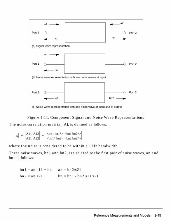
Figure 1-11. Component Signal and Noise Wave Representations
The noise correlation matrix, [A], is defined as follows:
where the noise is considered to be within a 1 Hz bandwidth.
These noise waves, bn1 and bn2, are related to the first pair of noise waves, an andbn, as follows:
bn1 = an s11 + bn an = bn2/s21
bn2 = an s21 bn = bn1 - bn2 s11/s21
Port 1 Port 2
a1
b1
a2
b2
(a) Signal wave representation
Port 1 Port 2
an
bn
Port 1 Port 2
bn1 bn2
(c) Noise wave representation with one noise wave at input and at output
(b) Noise wave representation with two noise waves at input
AA11 A12
A21 A22
<bn1 bn1*> <bn1 bn2*>
<bn1* bn2> <bn2 bn2*>= =
Reference Measurements and Models 1-45

RF System Budget Analysis
This results in the following relationship between the [A] and [N] noise correlationparameters:
A11 = N22 |s11|2 + N21 s11 + N12 s11* + N11
A12 = N22 s11 s21* + N12 s21*
A21 = N22 s11* s21 + N21 s21
A22 = N22 |s21|2
N11 = A11 + A22 |s11|2/|s21|2 - A12 s11*/s21* - A12* s11/s21
N12 = A12/s21* - A22 s11/|s21|2
N21 = A21/s21 - A22 s11*/|s21|2
N22 = A22/|s21|2
Linear Component Noise Models
A two-port linear circuit component has a mathematical model defined by a 2x2S-parameter matrix and a 2x2 noise wave parameter matrix. The linear componentmay be passive or active.
A passive component has S-parameters that satisfy the energy conservationrequirement for port index i from 1 to N:
The noise wave parameters for a linear passive component are derived from thecomponent S-parameters and its physical temperature as follows:
For an n-port passive component the noise correlation matrix is given by reference[3]:
[A] = k • Tphys • {[I] - [s][s*]T}
where:
Tphys = physical temperature in K
[I] = the identity matrix
[s] = the component’s S-parameter matrix
[s*]T = the transpose of the conjugate of the [s] matrix
Sij2
1≤j 1=
N
∑
1-46 Reference Measurements and Models

For a two-port component:
The [N] noise correlation matrix may be derived from this [A] matrix.
All active linear components within the program are two-port components with noisewave parameters that are related to the more common noise parameters of NFmin,Gopt, and Rn (minimum noise (dB), optimum source reflection coefficient for NFmin,equivalent input normalized noise resistance, respectively) as follows (see reference[1]):
N11 = k Tb T0N12 = k Tc T0 (cos(phi) + j sin(phi))N21 = k Tc T0 (cos(phi) - j sin(phi))N22 = k Ta T0
where:
These noise correlation parameters, Nij, can be converted back to the standard noiseparameters as follows:
k Td = 0.5 {(N22+N11) + sqrt((N22+N11)2 - 4 |N12|2)}NFmin = 10 log10(Td + 1 + N11/k)|Gopt| = |N12/k|/(Td)angle(Gopt) = PI - angle(N12/k)Rn = Td/4 | 1+Gopt|2
k = Boltzmann’s constant
T0 = reference temperature = 290 K
Ta = Fmin - 1 + Td |Gopt|2
Tb = Td - Fmin + 1
Tc = Td |Gopt|
phi = PI - angle(Gopt)
Td = 4 Rn/ | 1 + Gopt |2
Fmin = 10(NFmin / 10)
angle(Gopt) = angle of Gopt
Z0 = reference resistance
A11 A12
A21 A22k Tphys 1 0
0 1
s11 s12
s21 s22
s11* s21*
s12* s22*–
••=
Reference Measurements and Models 1-47
RF System Budget Analysis
The component noise is dependent on the source reflection coefficient, Gams, asfollows (see reference [1]):
NF = 10 log10(nf)
where:
There is a physical realizability requirement for the noise parameters of an activetwo-port. This requirement may be expressed with respect to the common noiseparameters of NFmin, Gopt, and Rn (minimum noise in dB, optimum sourcereflection coefficient for NFmin, equivalent input normalized noise resistance,respectively) as follows:
The requirement is based on the component’s minimum noise temperature, Tmin,given as the following (see reference [4]):
where:
Any active component has its noise parameters checked against this physicalrequirement. If the noise parameters supplied by the user in any component are suchthat the Rn value supplied is less than this minimum, then the specific componentmodel will either error out and quit with error message to the user or will proceed bysetting the Rn value to this limit value.
Nonlinear Component Models
All nonlinear circuit components are two-port components with a mathematicalmodel defined by a 2x2 S-parameter matrix versus input power at port 1 and port 2,and a 2x2 noise wave parameter matrix derived at small-signal conditions.
In general, all S-parameters (s11, s12, s21, s22) vary as a function of input power.The parameters s11 and s21 are defined as a function of power incident at port 1 withno power incident at port 2; whereas s12 and s22 are defined as a function of power
Yopt = optimum source admittance normalized to 0.02 mhos
= (1 - Gopt) / (1 + Gopt)
nf 1 N22 N11 Gams2
2 Gams N12 angle Gams( ) angle N12( )+( )cos+ +
k 1 Gams2
–( )----------------------------------------------------------------------------------------------------------------------------------------------------------------------------+=
Rn (Fmin-1) 1+Gopt2
4⁄ 1 Gopt2
–( )⁄•≥
Tmin 4 Rn• RE[Yopt]• TO•≤
1-48 Reference Measurements and Models
incident at port 2 (see reference [5]). The data set for this nonlinear model is readilymeasured for a nonlinear RF two-port in a hardware measurement lab.
This data set has been accepted as a convenient means of characterizing nonlineardevices by their large-signal S-parameters and have been successfully used fordesigning power amplifiers, oscillators, etc. (see references [6], [7], [8]).
This general model for a circuit component nonlinearity is derived during a systemsimulation for a nonlinear component. For details about the P2D data file format, seeP2D Format in the chapter “Working with Data Files” in the Using CircuitSimulators documentation.
The noise wave parameters for an electrical nonlinearity are the same as thosedefined for an active linear component in “Linear Component Noise Models” onpage 1-46.
Characterization of Component Nonlinearities
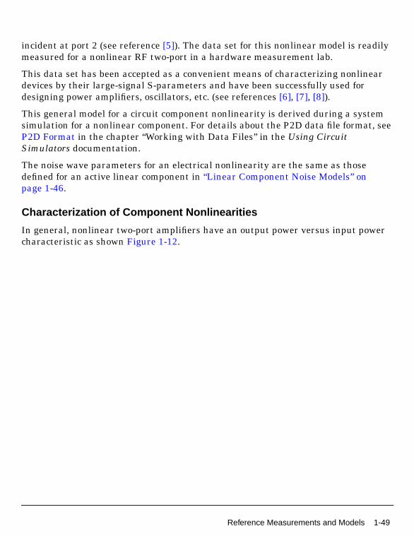
In general, nonlinear two-port amplifiers have an output power versus input powercharacteristic as shown Figure 1-12.
Reference Measurements and Models 1-49

RF System Budget Analysis
Figure 1-12. Nonlinear Component Characterization for Power Out Versus Power In
As shown, the nonlinear characteristic includes:
• Fundamental small-signal linear gain
• 2nd-order products
• 3rd-order products
• 5th and higher order products
• 3rd-order intercept point (IP3, also called TOI)
• 2nd-order intercept (IP2, also called SOI)
• 1 dB gain compression point (1DBC)
• Power saturation point (PSat)
• Gain compression at saturation (Gcs)
Output Power(dBm)
Input Power(dBm)
IP3
PSat
1DBC
1 dB
2nd order products
3rd order products
5th order products
Gcs
Linear gain
1-50 Reference Measurements and Models
For budget analysis, nonlinear two-port amplifiers are modeled using one of thefollowing modeling techniques:
• Nonlinear models with S-parameters versus power used for all nonlinearmeasurements except for SOI and TOI measurements.
• Nonlinear models with defined SOI used for SOI measurements.
• Nonlinear models with defined TOI used for TOI measurements.
• Nonlinear models with no explicitly defined TOI used for TOI measurements.
All nonlinear models represent zero memory nonlinearities.
Nonlinear models with S-parameters versus power
This nonlinear model is used for all nonlinear measurements except for SOI and TOImeasurements. It is based on the large-signal S-parameter (P2D) data set for eachnonlinear component. This data set is obtained for each nonlinear component duringbudget analysis set-up. In this data set, all S-parameters (S11, S21, S12, S22) canvary as a function of frequency and power. This data set is linearly interpolated andused for budget analysis.
The P2D data for a nonlinear component is collected at the component inputfrequency and for a power range that is dependant on whether the user has selectedany budget measurements that require the 1 dB power compression point (P1dB) foreach component.
When no P1dB measurement is selected: The maximum component input power usedto collect the P2D data for a nonlinear component is equal to the componentlarge-signal incident power (P_LS_inc) plus 5 dB (P_LS_inc+5dB). The large-signalincident power is determined by analyzing the system to determine the systemlarge-signal gain from the system source output to the evaluated nonlinearcomponent input. This maximum power level (P_LS_inc+5dB) must be less than orequal to the CmpMaxPin value (Component maximum input power in dBm). You canset CmpMaxPin in the Budget controller’s setup dialog box, on the Setup tab.
When any P1dB measurement is selected: The maximum component input power usedto collect the P2D data for a nonlinear component is equal to the componentsmall-signal incident power (P_SS_inc) that places the nonlinear component into atleast 5 dB gain compression (P_SS_inc_5dB). The small-signal incident power isdetermined by analyzing the system to determine the system small-signal gain fromthe system source output to the evaluated nonlinear component input. Thismaximum power level (P_LS_inc_5dB) must be less than or equal to the CmpMaxPinvalue (Component maximum input power in dBm). You can set CmpMaxPin in the
Reference Measurements and Models 1-51

RF System Budget Analysis
Budget controller’s setup dialog box, on the Setup tab. The P1dB measurements areany of the following: Cmp_OutP1dB_dBm, InP1dB_dBm, OutCDR_ResBW_dB,OutCDR_Total_dB, OutP1dB_dBm.
Given the component maximum input power from the above conditions(P_LS_inc+5dB or P_SS_inc_5dB), the P2D data (S11, S12, S21, S22 versus power) isobtained for the nonlinear component over a 100 dB range below this maximuminput power in 1 dB steps.
During budget analysis, the P2D data for each nonlinear component is linearlyinterpolated in an iterative process to obtain the overall system operating points ateach nonlinear component input and output. All P2D S-parameters (S11, S12, S21,S22) are used in this analysis.
Nonlinear models with defined SOI used for SOI measurements
This nonlinear model is used only for components Amplifier, Amplifier2, andAGC_Amp, and only when these models are at the top level of the RF System designbeing analyzed. If these models are within a nonlinear subnetwork design, then thesubnetwork is considered to not have any defined SOI and the nonlinear subnetworkis modeled as described in the section “Nonlinear models with S-parameters versuspower” on page 1-51.
For components Amplifier, Amplifier2 and AGC_Amp, SOI can only be used if TOI isalso specified.
The SOI value for these nonlinear amplifiers is used directly in the Budget SOImeasurements Cmp_OutSOI_dBm, InSOI_dBm, OutIM2_dBm, OutSOI_dBm.
For a definition of these measurements, see sections “Component Measurements” onpage 1-33, “System Measurements at Component Inputs” on page 1-35 and “SystemMeasurements at Component Outputs” on page 1-36.
Nonlinear models with defined TOI used for TOI measurements
This nonlinear model is used only for components Amplifier, Amplifier2 andAGC_Amp and only when these models are at the top level of the RF system designbeing analyzed. If these models are within a nonlinear subnetwork design, then thenonlinear subnetwork is modeled as described in the section for “Nonlinear modelwith no explicitly defined TOI used for TOI measurements” on page 1-53.
The TOI value for these nonlinear amplifiers is used directly in the Budget TOImeasurements Cmp_OutTOI_dBm, InTOI_dBm, OutIM3_dBm, OutTOI_dBm,OutSFDR_ResBW_dB, OutSFDR_Total_dB, OutS_IM3_dB.
1-52 Reference Measurements and Models
For definition of these measurements, see sections “Component Measurements” onpage 1-33, “System Measurements at Component Inputs” on page 1-35, and “SystemMeasurements at Component Outputs” on page 1-36.
Nonlinear model with no explicitly defined TOI used for TOI measurements
This nonlinear model is used for any nonlinear component with no defined TOI or forany nonlinear subnetwork for which TOI measurements are to be made.
The TOI value for these nonlinear amplifiers is derived from their P2D dataset forS21 versus power, and then these models are treated the same as for those describedin “Nonlinear models with defined TOI used for TOI measurements” on page 1-52.
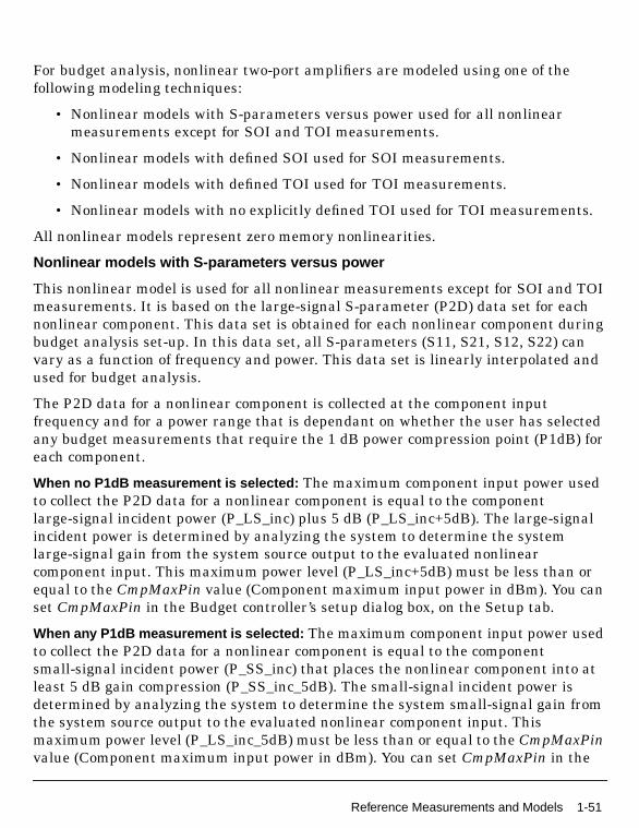
The TOI value is obtained by curve fitting the component S21 data versus power to athird order polynomial expression evaluated under low power conditions. It ispresumed that the nonlinear model does not contain any SOI characteristic.
The 3rd-order polynomial expression relates output RF voltage (Vout) to input RFvoltage (Vin).
where:
The S21 data versus power (Vout versus Vin) is used to find the input signal levelwhere 0.2 dB gain compression occurs (Vin_0.2dB). It is presumed that only the3rd-order nonlinearity dominates at this level of gain compression and that all higherorder nonlinear polynomial terms are negligible.
Given the small-signal gain (a1) and the value for Vin_0.2dB, the a3 coefficient (andthus the TOI value) is derived.
For details on how a3 and TOI are related, see the section “2nd and 3rd-OrderIntercept Definition” on page 1-64.
Vin = input signal voltage
Vout = output signal voltage
a1 = small-signal gain
a3 = 3rd-order gain coefficient
Vout Vin( ) a1Vin a3Vin3
+=
Reference Measurements and Models 1-53
RF System Budget Analysis
LimitationsWhen using the Budget controller, you must be aware of various simulatorconditions, constraints, and limitations, so that you can be more effective inaddressing subsystem and system design, and simulation objectives.
Budget analysis determines the system internodal signal and noise performance forcomponents in the top level system network. Budget analysis uses frequency-domainbased S-parameter and noise wave parameter techniques for a system containingonly components for which S-parameter and noise wave parameters are meaningful.The analysis is a single-tone analysis.
Budget controller analysis has the following simulator conditions, constraints, andlimitations:
• The system input signal source must have an output resistance of 50 ohms, butmay have a user-defined temperature.
• The signal source has a single fundamental frequency defined for systembudget analysis. An optional second fundamental frequency may be defined forcontrol of system AGC loops.
• The system output termination load must be 50 ohms and is assumed to benoiseless.
• The system network and all top level system components and subnetworksmust have only two ports, with the only exceptions being: AGC_Amp,AGC_PwrControl, S2P, PathSelect2, or R with pin 2 tied to ground.
• All subnetworks must result in a single frequency tone at its output that is thesame as the frequency at the subnetwork input.
• Noise analysis is performed for all nonlinear amplifiers operating in their linearregion. This implies that the noise characteristic is not dependant on thenonlinear operating point.
• All nonlinear components are assumed to be memory-less nonlinearities. Thismeans that their nonlinear characteristic is not dependant on the time historyof the input signal.
• All nonlinear components are defined based on the compression effects on asingle fundamental RF tone input. This implies that LO and image frequenciesdo not impact the nonlinear characteristics for the single fundamental RF tone.
1-54 Limitations
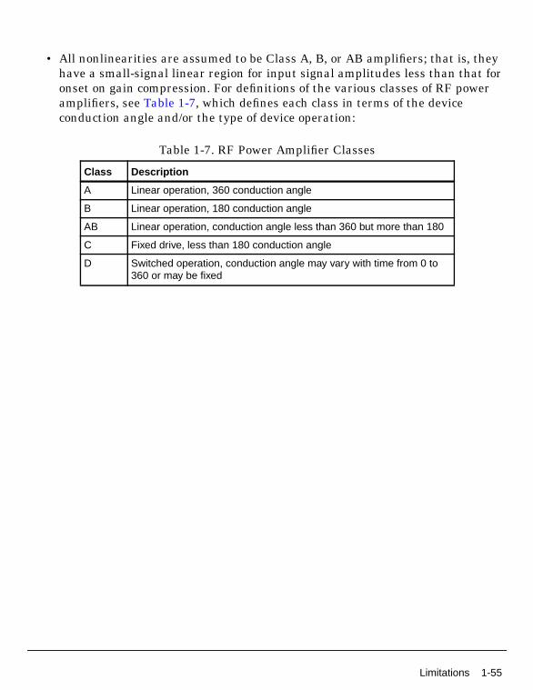
• All nonlinearities are assumed to be Class A, B, or AB amplifiers; that is, theyhave a small-signal linear region for input signal amplitudes less than that foronset on gain compression. For definitions of the various classes of RF poweramplifiers, see Table 1-7, which defines each class in terms of the deviceconduction angle and/or the type of device operation:
Table 1-7. RF Power Amplifier Classes
Class Description
A Linear operation, 360 conduction angle
B Linear operation, 180 conduction angle
AB Linear operation, conduction angle less than 360 but more than 180
C Fixed drive, less than 180 conduction angle
D Switched operation, conduction angle may vary with time from 0 to360 or may be fixed
Limitations 1-55
RF System Budget Analysis
ParametersThe recommended way to setup a budget analysis is by using the Budget controllerset up dialog box. To open this dialog box, double-click the Budget controller instancefrom the ADS schematic design. The Budget dialog box includes three tabs, enablingyou to define the following aspects of the simulation:
• Setup —Provides simulation setup and results/display setup features.
• Measurements —Provides measurement descriptions, selection, save and recallfeatures.
• Display —Control the visibility of simulation parameters on the Schematic. Fordetails, refer to the topic “Displaying Simulation Parameters on the Schematic”in the chapter “Simulation Basics” in the Using Circuit Simulatorsdocumentation.
1-56 Parameters
Setting up a Budget Analysis
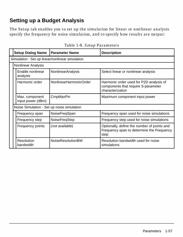
The Setup tab enables you to set up the simulation for linear or nonlinear analysisspecify the frequency for noise simulation, and to specify how results are output:
Table 1-8. Setup Parameters
Setup Dialog Name Parameter Name Description
Simulation - Set up linear/nonlinear simulation
Nonlinear Analysis
Enable nonlinearanalysis
NonlinearAnalysis Select linear or nonlinear analysis
Harmonic order NonlinearHarmonicOrder Harmonic order used for P2D analysis ofcomponents that require S-parametercharacterization
Max. componentinput power (dBm)
CmpMaxPin Maximum component input power
Noise Simulation - Set up noise simulation
Frequency span NoiseFreqSpan Frequency span used for noise simulations
Frequency step NoiseFreqStep Frequency step used for noise simulations
Frequency points (not available) Optionally, define the number of points andFrequency span to determine the Frequencystep
Resolutionbandwidth
NoiseResolutionBW Resolution bandwidth used for noisesimulations
Parameters 1-57

RF System Budget Analysis
Results - Set up the format and options for displaying results after analysis
Components in TableComponentFormat Formats output table with measurements incolumns or rows
Angle unit MeasurementAngleUnit Determines the angle for outputmeasurements in radians or degrees
Frequency unit MeasurementFrequencyUnit Determines the frequency units for outputmeasurements in Hz, kHz, MHz, GHz, or THz
Auto format displaywith overwrite
AutoFormatDisplay When selected, the output to the DataDisplay is formatted in tables and plots suchthat:- Components are ordered as in the systemfrom first to last (source to term)- Measurements are ordered as listed in theMeasurement tab- New data overwrites the existing .dds file forthe current design
Output results ascomma separatedvalues (CSV) to file
OutputCSVFile Measurement data written ascomma-separated values to .csv file
Run command afteranalysis
RunCommand When Output results as comma separatedvalues (CSV) to file is selected, enabling thisparameter runs a user-defined commandafter analysis. The command is entered inthe System Command field, and typically isused for post processing the .csv file data.
System command SystemCommand When Run command after analysis isselected, enter a command to run, such asrunning Excel on a PC platform. See“Exporting and Post-ProcessingResults” on page 1-26.
Table 1-8. Setup Parameters
Setup Dialog Name Parameter Name Description
1-58 Parameters

Selecting Measurements
The Measurement tab enables you to select system cascade measurements that areevaluated per component in the schematic design.
Note Measurements also include a set of built-in measurements that summarizeoverall system performance. These are single value system summary measurementsand are not for each component. They are not selectable, and are always written tothe CSV file and the ADS dataset.
Table 1-9. Measurements Parameters
Setup DialogName Parameter Name Description
Recall selectedmeasurementsfrom file
Populates the list of Selected Measurementsfrom a file
AvailableMeasurements
Select from list of available measurements toinclude in analysis. These are system cascademeasurements for each component, or at eachcomponent input or output.
To place measurements onto the SelectedMeasurements list, select measurement(s), thenclick Add.
SelectedMeasurements
Measurement[n] An ordered list determines the order in whichmeasurements are written to the CSV file andData Display.
To change the order:- Raise moves the selected measurement up- Lower moves the selected measurement down- Delete moves selected measurement(s) to theAvailable Measurements list
Description Displays description of selected measurement
Save selectedmeasurements tofile
Saves the list of selected measurement to a textfile
Parameters 1-59
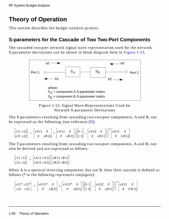
RF System Budget Analysis
Theory of OperationThis section describes the budget analysis process.
S-parameters for the Cascade of Two Two-Port Components
The cascaded two-port network signal wave representation used for the networkS-parameter derivations can be shown in block diagram form in Figure 1-13.
Figure 1-13. Signal Wave-Representations Used forNetwork S-parameter Derivations
The S-parameters resulting from cascading two two-port components, A and B, canbe expressed as the following: (see reference [9])
The T-parameters resulting from cascading two two-port components, A and B, canalso be derived and are expressed as follows:
When A is a spectral inverting component, but not B, then their cascade is defined asfollows (* in the following represents conjugate):
Port 1 Port 2
a1
b1
a2
b2
SA SB
where:SA = component A S-parameter matrixSB = component B S-parameter matrix
s11 s12
s21 s22
sA11 0
0 sB22
sA12 0
0 sB21
0 1
1 0
sA22 0
0 sB11–
1–
sA21 0
0 SB12+=
t11 t12
t21 t22
tA11 tA12
tA21 tA22
tB11 tB12
tB21 tB22=
s11* s12*
s21 s22
sA11* 0
0 sB22
sA12* 0
0 sB21
0 1
1 0
sA22 0
0 sB11–
1–
sA21 0
0 SB12+=
1-60 Theory of Operation
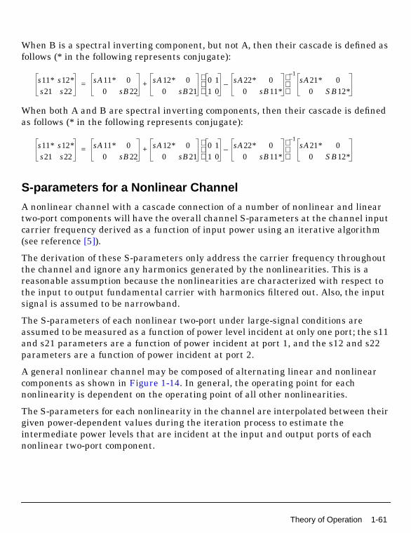
When B is a spectral inverting component, but not A, then their cascade is defined asfollows (* in the following represents conjugate):
When both A and B are spectral inverting components, then their cascade is definedas follows (* in the following represents conjugate):
S-parameters for a Nonlinear Channel
A nonlinear channel with a cascade connection of a number of nonlinear and lineartwo-port components will have the overall channel S-parameters at the channel inputcarrier frequency derived as a function of input power using an iterative algorithm(see reference [5]).
The derivation of these S-parameters only address the carrier frequency throughoutthe channel and ignore any harmonics generated by the nonlinearities. This is areasonable assumption because the nonlinearities are characterized with respect tothe input to output fundamental carrier with harmonics filtered out. Also, the inputsignal is assumed to be narrowband.
The S-parameters of each nonlinear two-port under large-signal conditions areassumed to be measured as a function of power level incident at only one port; the s11and s21 parameters are a function of power incident at port 1, and the s12 and s22parameters are a function of power incident at port 2.
A general nonlinear channel may be composed of alternating linear and nonlinearcomponents as shown in Figure 1-14. In general, the operating point for eachnonlinearity is dependent on the operating point of all other nonlinearities.
The S-parameters for each nonlinearity in the channel are interpolated between theirgiven power-dependent values during the iteration process to estimate theintermediate power levels that are incident at the input and output ports of eachnonlinear two-port component.
s11* s12*
s21 s22
sA11* 0
0 sB22
sA12* 0
0 sB21
0 1
1 0
sA22* 0
0 sB11*–
1–
sA21* 0
0 SB12*+=
s11* s12*
s21 s22
sA11* 0
0 sB22
sA12* 0
0 sB21
0 1
1 0
sA22* 0
0 sB11*–
1–
sA21* 0
0 SB12*+=
Theory of Operation 1-61

RF System Budget Analysis
Figure 1-14. Cascade Connection of Alternately ConnectedLinear and Nonlinear Two-Port Components
In Figure 1-14:
• Pin is the power incident at the channel input (at a given carrier frequency).
• PO(n) and QO(n) are the initial estimates of the incident power levels at theinput and output ports of the n’th nonlinearity obtained from an initialsmall-signal analysis.
• PK(n) and QK(n) are the incident power levels at the k’th iteration.
• G1K(n) and G2K(n) are the total reflection coefficients looking into the inputand output ports of n’th nonlinearity calculated at the k’th iteration.
• The (k+1) terms are derived from the k estimates.
• PT(n) and QT(n) are the operating power levels incident at port 1 and port 2 ofthe n’th nonlinearity obtained after the final iteration.
The iterative process is continued until the change in PT and QT is below apredetermined threshold. S-parameters for each nonlinearity are then obtained forthe PT(n) and QT(n) values and the overall channel S-parameters are derived as inthe linear case.
The greatest advantage of this technique is its ability to incorporate all the interstagemismatches and to handle any number of embedded linear and nonlinear two-portcomponents.
PT(1)
N1 N2 Nn
PK(1)
PO(1)
PT(2)QT(1) PT(n)QT(2) QT(n)
PO(2)QO(1)
PK(2)QK(1)
PO(n)QO(2)
PK(n)QK(2)
QO(n)
QK(n)
Pin
G1K(1) G1K(2) G1K(n)
G2K(n)G2K(2)G2K(1)
1-62 Theory of Operation
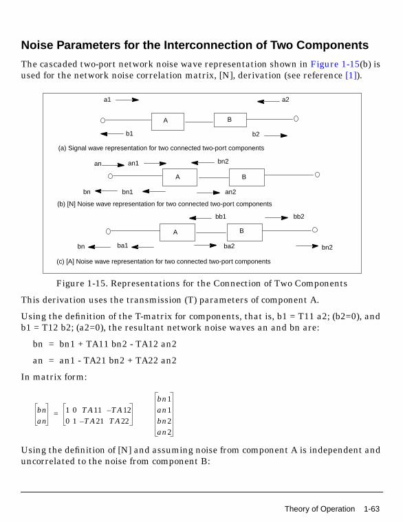
Noise Parameters for the Interconnection of Two Components
The cascaded two-port network noise wave representation shown in Figure 1-15(b) isused for the network noise correlation matrix, [N], derivation (see reference [1]).
Figure 1-15. Representations for the Connection of Two Components
This derivation uses the transmission (T) parameters of component A.
Using the definition of the T-matrix for components, that is, b1 = T11 a2; (b2=0), andb1 = T12 b2; (a2=0), the resultant network noise waves an and bn are:
bn = bn1 + TA11 bn2 - TA12 an2
an = an1 - TA21 bn2 + TA22 an2
In matrix form:
Using the definition of [N] and assuming noise from component A is independent anduncorrelated to the noise from component B:
a1
b1
a2
b2
(a) Signal wave representation for two connected two-port components
(c) [A] Noise wave representation for two connected two-port components
an
bn1
(b) [N] Noise wave representation for two connected two-port components
A
A B
B
an1 bn2
an2bn
A B
bb1
bn ba2ba1
bb2
bn2
bnan
1 0 TA11 TA12–
0 1 TA21– TA22=
bn1
an1
bn2
an2
Theory of Operation 1-63
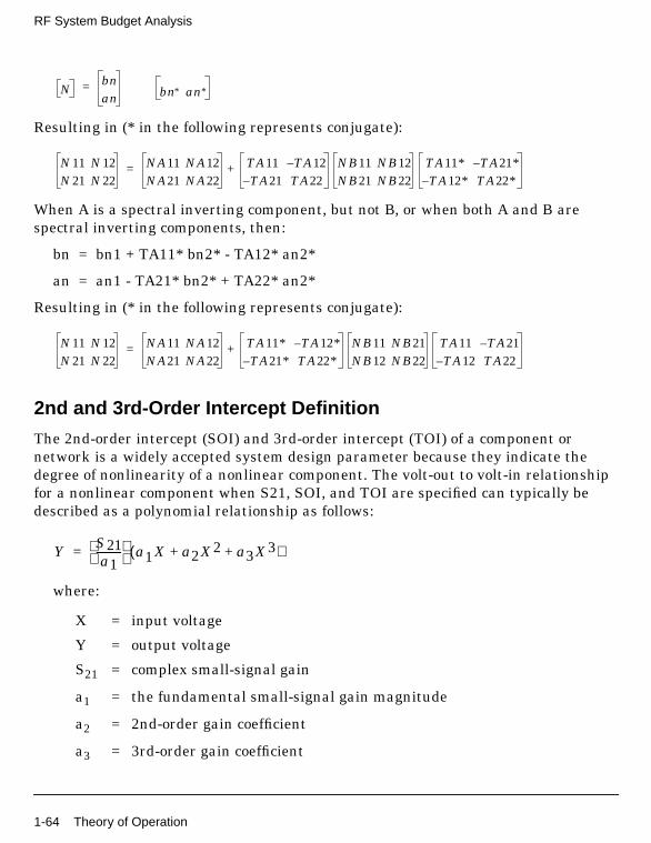
RF System Budget Analysis
Resulting in (* in the following represents conjugate):
When A is a spectral inverting component, but not B, or when both A and B arespectral inverting components, then:
bn = bn1 + TA11* bn2* - TA12* an2*
an = an1 - TA21* bn2* + TA22* an2*
Resulting in (* in the following represents conjugate):
2nd and 3rd-Order Intercept Definition
The 2nd-order intercept (SOI) and 3rd-order intercept (TOI) of a component ornetwork is a widely accepted system design parameter because they indicate thedegree of nonlinearity of a nonlinear component. The volt-out to volt-in relationshipfor a nonlinear component when S21, SOI, and TOI are specified can typically bedescribed as a polynomial relationship as follows:
where:
X = input voltage
Y = output voltage
S21 = complex small-signal gain
a1 = the fundamental small-signal gain magnitude
a2 = 2nd-order gain coefficient
a3 = 3rd-order gain coefficient
Nbnan
= bn* an*
N11 N12
N21 N22
NA11 NA12
NA21 NA22
TA11 TA12–
TA21– TA22
NB11 NB12
NB21 NB22
TA11* TA21*–
TA12*– TA22*+=
N11 N12
N21 N22
NA11 NA12
NA21 NA22
TA11* TA12*–
TA21*– TA22*
NB11 NB21
NB12 NB22
TA11 TA21–
TA12– TA22+=
Y S21a1
---------- a1X a2X2 a3X3+ +( )=
1-64 Theory of Operation

Given an input signal, Vin, with two frequency domain spectral tones (two-tones), ω1and ω2, such that ω2 > ω1 and (ω2-ω1) << ω1, then a nonlinear component’s outputintermodulation products will include 2nd-order intermodulation products at (ornear) twice ω1 and ω2 (2*ω1, 2*ω2, ω1+ω2), and 3rd-order intermodulation productslocalized about the two output fundamental tones (2*ω1-ω2, 2*ω1-ω2).
For a plot of the output power versus input power for output fundamental, 2nd-orderand 3rd-order tones, see Figure 1-12.
The small-signal fundamental curve varies with a 1:1 slope. The small-signal2nd-order and 3rd-order curves vary with a 2:1 and 3:1 slope respectively.
The third-order intercept is that point where the extrapolated small-signalfundamental and 3rd-order curves intersect. At this 3rd-order intercept you may beinterested in the input power level, or in the output power level.
Similarly, the 2nd-order intercept is that point where the extrapolated small-signalfundamental and 2nd-order curves intersect.
The following defines the nonlinear amplifier output response for one- and two-toneinputs, and derives the relationship between a2, a3 and SOI, TOI.
Nonlinearity Output for One- and Two-Tone Excitation
For one-tone excitation:
The response is:
For two-tone excitation:
x t( ) A1 ω1t( )cos=
y t( )a2
2----- A1
2 a1A1
3a3
4--------- A1
3+
ω1t( )a2
2----- A1
2
2ω1t( )
a3
4----- A1
3
3ω1t( )cos+cos+cos+=
x t( ) A1 ω1t( ) A2 ω2t( )cos+cos=
Theory of Operation 1-65
RF System Budget Analysis
The response is:
+
+
+
+
+
+
For practical nonlinear devices defined by SOI and TOI, there is a maximum inputsignal level beyond which the device is driven into saturation. The above equationsare applicable only below this saturation drive level.
Below saturation, the a2 term is dependant on SOI (and not TOI) and that the a3term is dependant on TOI (and not SOI).
Relating Coefficients a 2 and a3 to a1, SOI and TOI
The a2 and a3 coefficients are derived from the nonlinear amplifier small-signal gainmagnitude, a1, and output SOI and TOI values.
Given SOI and TOI in dBm power units and given that the amplifier is defined withrespect to RefR input and output resistance, they also define the following:
SOI output power level, Watts = po_soi = 10( (SOI-30)/10) = vo_soi2/(2*RefR)
TOI output power level, Watts = po_toi = 10( (TOI-30)/10) = vo_toi2/(2*RefR)
SOI input power level, Watts = pi_soi = po_soi/(a12)
TOI input power level, Watts = pi_toi = po_toi/(a12)
y t( )a2
2----- A1
2 A22
+( ) a1A1
3a3
4--------- A1
3 3a3
2--------- A1A2
2+ +
ω1t( )cos+=
a1A2
3a3
4--------- A2
3 3a3
2--------- A2A1
2+ +
ω2t( )cos
a2
2----- A1
2
2ω1t( )
a2
2----- A2
2
2ω2t( )cos+cos
a3
4----- A1
3
3ω1t( )
a3
4----- A2
3
3ω2t( )cos+cos
a2A1A2( ) ω1 ω2–( )t( ) a2A1A2( ) ω1 ω2+( )t( )cos+cos
a3
4----- A2A1
2
2ω1 ω2+( )t( )
a3
4----- A2A1
2
2ω1 ω2–( )t( )cos+cos
a3
4----- A1A2
2
2ω2 ω1+( )t( )
a3
4----- A1A2
2
2ω2 ω1–( )t( )cos+cos
1-66 Theory of Operation
SOI and TOI are defined with respect to two-tone inputs with equal amplitude andwith small frequency difference ( ω) such that ω1= ω0- ω and ω2= ω0+ ω.
For SOI, the output tones of interest are at 2*ω1 = 2*ω0-2* ω, 2*ω2 = 2*ω0+2* ωand ω1+ω2 = 2*ω0.
For TOI, the output tones of interest are at
|2*ω1-ω2| = ω0-3* ωor|2*ω2-ω1| = ω0+3* ω
At low level input power levels (dBm), the 1st, 2nd, and 3rd order output powers(dBm) vary versus input power (dBm) with ratios 1:1, 2:1, and 3:1 respectively.
By definition, the SOI and TOI points occur where the input and output power levels(dBm) are equal for the extrapolation of the small-signal power levels (dBm) for thefundamental and 2nd-order harmonics (SOI) or 3rd-order harmonics (TOI).
For example, given ω1 = 995 MHz at -30 dBm and ω2 = 1005 MHz at -30 dBm andnonlinear device with S21 = 20 dB, SOI = 50 dBm and TOI = 30 dBm, the 2nd orderand 3rd order output tones are at (1990 MHz, 2000 MHz, 2010 MHz) and (985 MHz,1015 MHz) respectively.
For TOI at 30 dBm, the output tones at 1005 MHz and 1015 MHz are at -10 dBm and-90 dBm respectively. TOI is related to the levels at 1005 MHz and 1015 MHz asfollows:
TOI = -90 + 3/2*(-10 - (-90)) = 30 dBm
For SOI at 50 dBm, the output tones at 1990 MHz, 2000 MHz and 2010 MHz are at-76 dBm, -70 dBm and -76 dBm respectively. The 2nd order product at 2000 MHz isthe largest. SOI is related to the levels at 1005 MHz and 2000 MHz as follows:
SOI = -70 + 2*(-10 - (-70)) = 50 dBm
For SOI, and from the above equations for two-tone excitation, the maximum 2ndorder output tone occurs at ω1+ω2 for which the relationship between a2 to a1 andSOI is as follows:
a2 = a12/sqrt(2*RefR*po_soi)
where po_soi = 10( (SOI-30)/10) with SOI in dBm
∆ ∆ ∆
∆ ∆
∆
∆
Theory of Operation 1-67
RF System Budget Analysis
For TOI, and from the above equations for two-tone excitation, the 3rd-order tones at|2*ω1-ω2| or |2*ω2-ω1| are the desired 3rd-order intermod tones for which therelationship between a3 to a1 and TOI is as follows:
pi_toi = vi_toi2/(2*RefR)
a3 = (4/3)*a13/(2*RefR*po_toi)
where po_toi = 10( (TOI-30)/10) with TOI in dBm
2nd and 3rd-Order Intercept for a Cascade Network
When N two-port nonlinear components are connected in cascade, the expression forthe overall output 2nd- and 3rd-order intercepts (see reference [13]) are as follows:
where:
where:
This expression is typically evaluated (see reference [13]) as a scalar equation byignoring each component’s reflection coefficients (s11 and s22), transmission phasecharacteristic (angle of s21), and reverse transmission coefficients (s12).
However, this expression becomes a close approximation to a complete complexnonlinear solution when the pg[i] and vg[i] terms include the effects of each
vsoi = overall output SOI in volts
vsoi[i] = i’th component output SOI in volts
vg[i] = system voltage gain (magnitude) from the i’thcomponent output to the system output
ptoi = overall output TOI in watts
ptoi[i] = i’th component output TOI in watts
pg[i] = system power gain (magnitude) from the i’thcomponent output to the system output
1vsoi-----------
1vsoi i[ ]vg i[ ]---------------------------------
i 1=
N
∑=
1ptoi------------
1ptoi i[ ] pg i[ ]----------------------------------
i 1=
N
∑=
1-68 Theory of Operation
component’s reflection coefficients (s11 and s22), transmission phase characteristic(angle of s21), and reverse transmission characteristic (s12).
The preceding expressions for the network 2nd-order and 3rd-order intercepts arebased on the small-signal performance of the individual components and on theextrapolated intersection of each components small-signal fundamental and2nd-order and 3rd-order Pout versus Pin curves.
This formulation given above is used by the program to derive the network input andoutput 2nd and 3rd-order intercepts (InSOI, OutSOI, InTOI and OutTOI) andassociated measurements utilizing these intercepts (Cmp_OutSOI_dBm,OutIM2_dBm, Cmp_OutTOI_dBm, OutIM3_dBm, OutSFDR_ResBW_dB,OutSFDR_Total_dB, OutS_IM3_dB). These measurements do not require anylarge-signal analysis, and thus are approximations to the network’s actuallarge-signal performance.
Raw Data Generated for an RF Budget Analysis
The cascaded two-port analysis described in the prior sections defined small-signalS-parameter analysis, power dependent S-parameter analysis, and noise parameteranalysis. Those analyses result in raw data from which the RF budget measurementsare derived. To define this raw data, several cascade system definitions are shownfirst:
System source definitions
• RefR = system source resistance = 50 (cannot be changed by user)
• TempS = system source temperature in Celsius
• FreqS (FreqPilot) = system source (AGC pilot) frequency
• PwrS, PwrS_dBm (PwrPilot) = system source (AGC pilot) available power in W,dBm
System load definitions
• RefR = system load resistance = 50 (cannot be changed by the user)
• TempL = system load temperature = -273.15 C (cannot be changed by the user)
Component definitions
• N = number of cascaded components
• n = component index; n = 0, 1, …, N-1
Theory of Operation 1-69
RF System Budget Analysis
Simulation setup parameters
• ResBW: user-defined resolution BW for noise measurements
• SimBW, SimFStep: SimBW is the user-defined BW over which noisemeasurements are swept in frequency with steps defined by SimFStep
Temporary data calculated during cascade analysis
• s11_ss[n], s12_ss[n], s21_ss[n], s22_ss[n], s11_ls[n], s12_ls[n], s21_ls[n],s22_ls[n]
• S-parameters from system input to component n output for small- andlarge-signal analysis
• b2_ss[n], b2_ls[n]
• System wave out from component n and incident on component n+1 based onsmall- and large-signal analysis
• b2[N-1] = system wave incident on system load; define b2[-1] = 0
• a2_ss[n], a2_ls[n]
• System wave at output of component n and reflected from component n+1based on small- and large-signal analysis
• a2_ss[N-1], a2_ls[N-1] = 0 because GL = 0
• Define a2[-1] = reflection from component 0 input
System raw data
With the cascade system definition above, the system raw data is defined here wheren represents the n’th component with the index starting at zero for the firstcomponent:
• F[n] = frequency (Hz) at component output
• Let F[-1] = FreqS
• F[N-1] = FreqL = system load frequency based on system input FreqS
• G_ss[n], G_ls[n] = reflection coefficient at component input for small- andlarge-signal analysis
• Let G[N] = GL = 0
1-70 Theory of Operation
• VGI_ss[n], VGI_ls[n] = voltage gain for wave incident on load at componentoutput over system input wave for small- and large-signal analysis input wave
• VGI[n] = b2[n]/as = s21[n]/(1 - s11[n]*Gs - s22[n]*G[n+1] -s12[n]*s21[n]*Gs*G[n+1] + s11[n]*s22[n]*Gs*G[n+1])
• When Gs = 0: VGI[n] = s21[n]/(1 - s22[n]*G[n+1])
• VGR_ss[n], VGR_ls[n] = for wave reflected by load at component output oversystem input wave for small- and large-signal analysis
• VGR[n] = a2[n]/as = G[n+1] (b2[n]/as)
• When Gs = 0: VGR[n] = G[n+1] s21[n]/(1 - s22[n]*G[n+1])
• P_ss[n], P_ls[n], Q_ss[n], Q_ls[n] = power incident into, reflected fromcomponent input for small- and large-signal analysis
• P[n] = PwrS|VGI[n-1]|2
• Q[n] = PwrS|VGR[n-1]|2 = |G[n]|2 P[n]
• PG_ss[n], PG_ls[n] = transducer power gain for power delivered into load atcomponent output for small- and large-signal analysis
• PG[n] = (1-|Gs|2)(1-|G[n+1]|2)|s21[n]|2 / |(1 - s11[n] Gs)(1 - s22[n]G[n+1])- s12[n] s21[n] Gs G[n+1] |2
• When Gs = 0:
PG[n] = (1-|G[n+1]|2) |s21[n]|2 / |1 – s22[n] G[n+1]|2
PG[n] = |VGI[n]|2 – |VGR[n]|2
Theory of Operation 1-71

RF System Budget Analysis
• NPwr[n] = noise power, dBm, at component output
where:
• NBW[n] = noise bandwidth at component output
• NBW[n] = NPwr_W[n]/NPwr0_W[n]
• NPwr0_W[j] = noise power per Hz at the center of the SimulationBW at thenode
FreqS_NBW[j] = system input frequencies contributing to component joutput within its SimBW centered at its primary frequency
j = frequency index of swept system source
k = Boltzmann’s constant
NFin[n,j] = NF_RefIn[n] for FreqS_NBW[j]
PGss[n,j] = PG_ss[n] for FreqS_NBW[j]
NPwr n[ ] 30 10 kSimFStep TempS 273.15 290 10
NFin n j,[ ]10
------------------------------
1–
+ +
PGss n j,[ ]
j 0=
M 1–
∑
log+=
1-72 Theory of Operation
• Noise figure from system input to component output, NF_RefIn[n]
• Derived from NPwr_NF (W/Hz): defined to be similar as NPwr, but withTempS replaced with 290
• NPwr_NF[n] = (k Ti[n] Gi [n] + k Ts Gi[n])
where:
The Noise Figure above is from system input to component n output andincludes all system input image noise.
Noise Figure from system input to component output
The Noise Figure from system input to component output, but excluding systeminput image noise is not the real system noise figure, but is also available for users:
• NF_RefIn_NoImage[n] = noise figure, dB, from system input to component noutput, with exclusion of all input image noise
This is available for user reference to compare to their Excel spreadsheetcalculations that do not include image noise.
• This is the same as NF_RefIn when each mixer in the system is preceded by anideal input image rejection filter.
Gi[n] = G1[n] + G2[n] + G3[n] … = total transducer power gain(ratio) from system input to component n output for systeminput fundamental and image frequencies
G1[n] = transducer power gain from system input to the component noutput at the system input frequency
Ti[n] = T1[n] + T2[n] + T3[n] … = total noise temperature (K)representing the system noise contribution at system inputfundamental and image frequencies
T1[n] = noise temperature representing the system noisecontribution from system input to the component n output atthe system input frequency
Ts = source noise temperature = T0 = 290
NF_RefIn[n] = 10 log10( (T[n] Gi[n] + T0 Gi[n])/(T0 G1[n] )
Theory of Operation 1-73
RF System Budget Analysis
Noise Figure from component input to system output
The Noise Figure from component input to system output available excludes systeminput image noise.
• NF_RefOut_NoImage[n] = noise figure, dB, from component n input to systemoutput, with exclusion of all input image noise
The Noise Figure contribution by the component to the overall system noisefigure excludes system input image noise.
• NF_Ctrb_NoImage[n] = component n contribution, in dB, to full system NF
Raw Data Summary for Budget Analysis
With the definitions above, Table 1-10 shows the raw data from which allmeasurements are related by formula.
Table 1-10. Raw Data Generated for an RF System Budget Analysis
Raw Data Name Description Notes
System_S12[j] System overall S12 j=0 for dB=1 for mag=2 for phase
System_S22[j] System overall S22 j=0 for dB=1 for mag=2 for phase
Cmp_Name[n] Component name n = 0 to N-1
Cmp_RefDes[n] Component reference designator name n = 0 to N-1
Cmp_Ctrb_SysNF_NoImage[n] System noise figure improvement in dBif component contributes no noise;excludes system input image noise
n = 0 to N-1
Cmp_Ctrb_SysTOI[n] System output 3rd-order interceptimprovement in dB if component islinear
n = 0 to N-1
Cmp_NF[n] Component noise figure in dB n = 0 to N-1
Cmp_OutP1[n] Component output 1 dB compressionpower level in dBm
n = 0 to N-1
Cmp_OutSOI[n] Component output 2nd-order interceptpower level in dB
n = 0 to N-1
Cmp_OutTOI[n] Component output 3rd-order interceptpower level in dBm
n = 0 to N-1
1-74 Theory of Operation

Cmp_S11[n, j] Component 50 ohm S11 n = 0 to N-1;j=0 for dB=1 for mag=2 for phase
Cmp_S12[n, j] Component 50 ohm S12 n = 0 to N-1;j=0 for dB=1 for mag=2 for phase
Cmp_S21[n, j] Component 50 ohm S21 n = 0 to N-1;j=0 for dB=1 for mag=2 for phase
Cmp_S22[n, j] Component 50 ohm S22 n = 0 to N-1;j=0 for dB=1 for mag=2 for phase
G_ss[n, j] Reflection coefficient at componentinput for small-signal analysis
n = 0 to N-1;j=0 for dB=1 for mag=2 for phase
G_ls[n, j] Reflection coefficient at componentinput for large-signal analysis
n = 0 to N-1;j=0 for dB=1 for mag=2 for phase
VGI_ss[n, j] Voltage gain for wave incident on loadat component output over system inputwave for small-signal analysis
n = 0 to N-1;j=0 for dB=1 for mag=2 for phase
VGI_ls[n, j] Voltage gain for wave incident on loadat component output over system inputwave for large-signal analysis
n = 0 to N-1;j=0 for dB=1 for mag=2 for phase
VGR_ss[n, j] Voltage gain for wave reflected by loadat component output over system inputwave for small-signal analysis
n = 0 to N-1;j=0 for dB=1 for mag=2 for phase
VGR_ls[n, j] Voltage gain for wave reflected by loadat component output over system inputwave for large-signal analysis
n = 0 to N-1;j=0 for dB=1 for mag=2 for phase
Table 1-10. Raw Data Generated for an RF System Budget Analysis
Raw Data Name Description Notes
Theory of Operation 1-75
RF System Budget Analysis
P_ss[n] Power in dBm incident into componentinput for small-signal analysis
n = 0 to N-1
P_ls[n] Power in dBm incident into componentinput for large-signal analysis
n = 0 to N-1
Q_ss[n] Power in dBm reflected fromcomponent input for small-signalanalysis
n = 0 to N-1
Q_ls[n] Power in dBm reflected fromcomponent input for large-signalanalysis
n = 0 to N-1
PG_ss[n] Transducer power gain in dB for powerdelivered into load at component outputfor small-signal analysis
n = -1 to N-1; -1 means atsystem source output
PG_ls[n] Transducer power gain in dB for powerdelivered into load at component outputfor large-signal analysis
n = -1 to N-1; -1 means atsystem source output
F[n] Frequency at component output n = -1 to N-1; -1 means atsystem source output
NF_refin[n] Noise figure in dB from system input tocomponent output
n = 0 to N-1
NF_refin_no_image[n] Noise figure in dB from system input tocomponent output; with exclusion of allimage noise
n = 0 to N-1
NF_refin_image_only[n] Noise figure in dB from system input tocomponent output; based only onimage noise
n = 0 to N-1
NF_refout_no_image[n] Noise figure in dB from componentinput to system output; with exclusionof all image noise
n = 0 to N-1
NPwr[n] Total noise power in dBm at componentoutput
n = -1 to N-1; -1 means atsystem source output
NPwr0[n] Noise power in dBm per resolutionbandwidth at component output
n = -1 to N-1; -1 means atsystem source output
NBW[n] Noise bandwidth at component output n = 0 to N-1
SOI_in[n] 2nd-order intercept power level in dBmat component input based onVGI_ls[n-1, 0]
n = 0 to N-1
Table 1-10. Raw Data Generated for an RF System Budget Analysis
Raw Data Name Description Notes
1-76 Theory of Operation
SOI_out[n] 2nd-order intercept power level in dBmat component output based onVGI_ls[n, 0]
n = 0 to N-1
TOI_in[n] 3rd-order intercept power level in dBmat component input based onVGI_ls[n-1, 0]
n = 0 to N-1
TOI_out[n] 3rd-order intercept power level in dBmat component output based onVGI_ls[n, 0]
n = 0 to N-1
P1dB_in[n] 1 dB gain compression power in dBmat component output based onVGI_ls[n-1, 0]
n = 0 to N-1
P1dB_out[n] 1 dB gain compression power in dBmat component output based onVGI_ls[n, 0]
n = 0 to N-1
Table 1-10. Raw Data Generated for an RF System Budget Analysis
Raw Data Name Description Notes
Theory of Operation 1-77

RF System Budget Analysis
TroubleshootingHere are some typical budget simulation problems and remedies to resolve them.
Using Components with Three or More Ports
Only two-port components are supported by the budget simulation, except for thesecomponents: AGC_Amp, AGC_PwrControl, S2P, PathSelect2, and R with pin 2 tied toground. The simulation will generate an error if any other unsupported componentshave three or more ports.
Using Unsupported Networks
If the topology in the design is not a simple two-port cascaded network, an error isgenerated indicating more than three components are connected in the network.Only two-port cascaded RF system designs can be used with the Budget controller.For example designs, see the “Performing Budget Simulations” on page 1-9.
Using Unsupported Components
If your design contains components that are not supported in a budget analysis, anerror is generated. The component may not be supported for one of the followingreasons:
• The component does not have an S-parameter representation.
• The component cannot be used with the ADS P2D analysis controller. This isone of the limitations of the Budget controller, since it relies on P2D analysis todetermine the nonlinear characteristics of RF system components.
Unfortunately, no workaround exists for these components. They are simply notsupported in a budget simulation.
1-78 Troubleshooting
Enabling Other Simulation Controllers in a Design
When performing a budget analysis, no other analysis can be enabled in a simulation.If other analyses are included, an error is generated indicating that the designcontains an instance of another ADS simulation controller, such as HarmonicBalance, DC, etc., or an ADS parent controller, such as Sweep, Optim, Yield, etc., thatdoes not sweep or optimize the budget analysis instance. The Budget controller canonly be used in isolation, except where parent controllers are used to sweep oroptimize the budget analysis. Remove any instances of these other ADS simulationcontrollers (DC, Harmonic Balance, S_Param) to proceed.
Setting the CmpMaxPin Parameter
If the value for the maximum component input power parameter (CmpMaxPin) is settoo low, the analysis cannot characterize nonlinearity. Increase the value of theBudget controller parameter CmpMaxPin and try again. For information about howCmpMaxPin is used with nonlinear models, see “Characterization of ComponentNonlinearities” on page 1-49.
Internal Errors
If a fatal internal error occurs, please report the problem to Agilent EEsof TechnicalSupport. Also, keep the design that is causing the error available for evaluation byAgilent EEsof.
Troubleshooting 1-79
RF System Budget Analysis
References[1]R.P. Meys. “A Wave Approach to the Noise Properties of Linear Microwave
Devices.” IEEE Transactions on Microwave Theory Techniques, Vol. MTT-26,No. 1, pp. 34-37, January 1978.
[2] N.G. Kanaglekar, R.E. McIntosh, and W.L. Bryant. “Wave Analysis of Noise inInterconnected Multiport Networks.” IEEE Transactions on Microwave TheoryTechniques, Vol. MTT-35, No. 2, pp. 112-116, February 1987.
[3] H. Bosma. “On the theory of linear noisy systems.” Phillips Research ReportsSupplement, No. 10, 1967.
[4] M. W. Pospiezalski. “On the Measurement of Noise Parameters of MicrowaveTwo-Ports.” IEEE Transactions on Microwave Theory and Techniques,Vol. MTT-34, No. 4, pp. 456-458, April 1986.
[5] N.G. Kanaglekar. “Noise, Intermodulation Distortion, and Large-SignalS-Parameter Analyses of Microwave Systems.” Ph.D. Dissertation, Dept. ofECE, University of Massachusetts at Amherst, May 1987.
[6] R.Tucher. “RF Characterization of Microwave Power FETs.” IEEE Transactionson Microwave Theory and Techniques, Vol. MTT-29, No. 8, pp. 776-781,August 1981.
[7] Gilmore and Rosenbaum. “An Analytic Approach to Optimum Oscillator DesignUsing S-parameters.” IEEE Transactions on Microwave Theory and Techniques,Vol. MTT-31, No. 8, pp. 633-639, August 1983.
[8] Mazumder and Puije. “Two-Signal Method of Measuring the Large-SignalS-parameters of Transistors.” IEEE Transactions on Microwave Theory andTechniques, Vol. MTT-26, No. 6, pp. 417-420, June 1978.
[9] K. C. Gupta, R. Garg and R. Chada. Computer-Aided Design of MicrowaveCircuits. Norwood:Artech House, 1981.
[10] M.E. Hines. “Inherent Signal Losses in Resistive-Diode Mixers.” IEEETransactions on Microwave Theory Techniques, Vol. MTT-29, No. 4, pp. 281-292,April 1981.
[11] Y. Taur. “Josephson-Junction Mixer Analysis Using Frequency-Conversion andNoise Correlation Matrices.” IEEE Transactions on Electron Devices,Vol. ED-27, pp. 1921-1928, October 1980.
[12] S.A. Maas. Microwave Mixers. Dedham:Artech House, 1985.
1-80 References

[13] S. E. Wilson. “Evaluate the Distortion of Modular Cascades.” Microwaves,pp. 67-70, March 1981.
[14] N. G. Kanaglekar, et. al. “Analysis of Two-Tone, Third-Order Distortion inCascaded Two-Ports.” IEEE Transactions on Microwave Theory Techniques,Vol. MTT-36, No. 4, pp. 701-705, April 1988.
References 1-81

RF System Budget Analysis
1-82 References
Index
AAGC control loops, 1-14, 1-54AGC_Amp, 1-7, 1-14AGC_PwrControl, 1-7, 1-14automatic formatting, 1-20-1-25display pages generated, 1-21enabling, 1-20plots, 1-25tables, 1-22, 1-23
Bbudget analysis
comparison of techniques, 1-4budget analysis functions
advantages, 1-4Budget controller
advantages, 1-4basic example, 1-10compared to generic budget analysis, 1-4introduction, 1-2-1-5license requirements, 1-6limitations, 1-54purpose, 1-1restrictions, 1-5using, 1-7
Ccascade measurements, 1-32-1-38Cmp_Ctrb_SysNF_NoImage[n], 1-74Cmp_Ctrb_SysNF_NoImage_dB, 1-33Cmp_Ctrb_SysTOI[n], 1-74Cmp_Ctrb_SysTOI_dB, 1-33Cmp_LS_GainChange_dB, 1-33Cmp_Name[n], 1-74Cmp_NF[n], 1-74Cmp_NF_dB, 1-33Cmp_OutN0_dBm, 1-33Cmp_OutP1[n], 1-74Cmp_OutP1dB_dBm, 1-33Cmp_OutSOI[n], 1-74Cmp_OutSOI_dBm, 1-33Cmp_OutTOI[n], 1-74Cmp_OutTOI_dBm, 1-33Cmp_RefDes[n], 1-74Cmp_S11[n, j], 1-75
Cmp_S11_dB, 1-33Cmp_S11_mag, 1-33Cmp_S11_phase, 1-33Cmp_S12[n, j], 1-75Cmp_S12_dB, 1-33Cmp_S12_mag, 1-33Cmp_S12_phase, 1-33Cmp_S21[n, j], 1-75Cmp_S21_dB, 1-33Cmp_S21_mag, 1-34Cmp_S21_phase, 1-34Cmp_S22[n, j], 1-75Cmp_S22_dB, 1-34Cmp_S22_mag, 1-34Cmp_S22_phase, 1-34Cmp_SS_MismatchLoss_dB, 1-34Cmp_SS_PGain_dB, 1-34CmpMaxPin, 1-51, 1-57, 1-79Comma Separated Values file. See CSV
filecomponent input measurements
list, 1-35component measurements
list, 1-33component models
components with spectral inversions,1-42
linear, 1-46nonlinear, 1-48nonlinearity characterization, 1-49two-port noise parameter, 1-43two-port small signal S-parameter, 1-41
component output measurementslist, 1-36
componentson Simulation-Budget palette, 1-7
CSV file, 1-26enabling output, 1-26post-processing with, 1-30
Ddata
list of raw data generated, 1-74data display template, 1-26design
Index-1

requirements, 1-2using Budget controller in, 1-7
designsexample project, 1-8
Eexamples, 1-8
AGC control loops, 1-14basic budget design, 1-10mixers, 1-12multiple paths, 1-12optimization and yield, 1-17sample spreadsheet, 1-28sweeping parameters, 1-16using data file as component, 1-13
FF[n], 1-76formatting results
automatic, 1-20-1-25in columns, 1-23in plots, 1-25in rows, 1-24in tables, 1-23system measurements, 1-22using data display template, 1-26
GG_ls[n, j], 1-75G_ss[n, j], 1-75
IInFreq, 1-35InNPwrTotal_dBm, 1-35InP1dB_dBm, 1-35InPGain_dB, 1-35InPGain_SS_dB, 1-35InPwr_dBm, 1-35InPwr_SS_dBm, 1-35InPwrInc_dBm, 1-35InPwrInc_SS_dBm, 1-35InPwrRefl_dBm, 1-35InPwrRefl_SS_dBm, 1-35InReflCoeff_dB, 1-35InReflCoeff_mag, 1-35InReflCoeff_phase, 1-35InReflCoeff_SS_dB, 1-35InReflCoeff_SS_mag, 1-35
InReflCoeff_SS_phase, 1-35InSNR0_dB, 1-36InSOI_dBm, 1-36InTE_K, 1-36InTOI_dBm, 1-36InVSWR, 1-36
Llicense requirements, 1-6linear component models, 1-46
Mmeasurements
at component inputs, 1-35at component outputs, 1-36cascade, 1-32-1-38component, 1-33noise figure, 1-34summary, 1-39-1-40system, 1-22
mixerexample, 1-12
Mixer2, 1-7MixerWithLO, 1-7, 1-13
NT1, 1-73Ti, 1-73NBW[n], 1-76NF_refin[n], 1-76NF_RefIn_dB, 1-34NF_refin_image_only[n], 1-76NF_refin_no_image[n], 1-76NF_RefIn_NoImage_dB, 1-34NF_refout_no_image[n], 1-76NF_RefOut_NoImage_dB, 1-34NFactor_RefIn_dB, 1-34noise, 1-54
in mixer example, 1-13in two-port network, 1-63matrix for linear component, 1-46on output load, 1-5parameter definitions, 1-43parameter setup, 1-57parameters for linear components, 1-46parameters for nonlinear component,
1-49temperature, 1-73
Index-2

noise figure, 1-73, 1-74list of measurements, 1-34
nonlinear component models, 1-48NPwr[n], 1-76NPwr0[n], 1-76
Ooptimization example, 1-17OutCDR_ResBW_dB, 1-36OutCDR_Total_dB, 1-36OutFreq, 1-36OutIM2_dBm, 1-36OutIM3_dBm, 1-36OutN0_dBm, 1-36OutNBW, 1-37OutNPwrResBW_dBm, 1-37OutNPwrTotal_dBm, 1-37OutP1dB_dBm, 1-37OutPGain_dB, 1-37OutPGainChange_dB, 1-37OutPwr_dBm, 1-37OutS_IM3_dB, 1-37OutSFDR_ResBW_dB, 1-37OutSFDR_Total_dB, 1-37OutSNR_ResBW_dB, 1-37OutSNR_Total_dB, 1-37OutSNR0_dB, 1-37OutSOI_dBm, 1-37OutTOI_dBm, 1-37OutVGainInc_dB, 1-38OutVGainInc_mag, 1-38OutVGainInc_phase, 1-38OutVGainInc_SS_dB, 1-38OutVGainInc_SS_mag, 1-38OutVGainInc_SS_phase, 1-38OutVGainRefl_dB, 1-38OutVGainRefl_mag, 1-38OutVGainRefl_phase, 1-38OutVGainRefl_SS_dB, 1-38OutVGainRefl_SS_mag, 1-38OutVGainRefl_SS_phase, 1-38
PP_1Tone, 1-7P_ls[n], 1-76P_nTone, 1-7P_ss[n], 1-76P1dB_in[n], 1-77
P1dB_out[n], 1-77PathSelect2, 1-7, 1-13PG_ls[n], 1-76PG_ss[n], 1-76plots, 1-25post-processing results, 1-26-1-31
enabling, 1-27usage, 1-27
QQ_ls[n], 1-76Q_ss[n], 1-76
Rreferences, 1-80results
exporting, 1-26post-processing, 1-26-1-31
RF designrequirements, 1-2
SS2P, 1-7Simulation-Budget palette, 1-7
components available, 1-7small signal
S-parameter definitions, 1-41SOI_in[n], 1-76SOI_out[n], 1-77S-parameters
derived from cascaded network, 1-60for components with spectral inversions,
1-42for nonlinear channel, 1-61in nonlinear models, 1-48matrix for linear component, 1-46raw data, 1-69small signal definitions, 1-41using file as component, 1-13
spreadsheet example, 1-28summary measurements, 1-39-1-40sweep example, 1-16system measurements, 1-22
list, 1-35, 1-36System_AnalysisType, 1-40System_NoiseResBW, 1-40System_NoiseSimBW, 1-40System_NoiseSimFStep, 1-40
Index-3

System_PilotFreq, 1-40System_PilotPwr_dBm, 1-40System_S12[j], 1-74System_S22[j], 1-74System_SourceFreq, 1-40System_SourcePwr_dBm, 1-40System_SourceTemp, 1-40SystemInN0_dBm, 1-39SystemInNPwr_dBm, 1-39SystemInP1dB, 1-39SystemInP1dB_dBm, 1-39SystemInSOI_dBm, 1-39SystemInTOI_dBm, 1-39SystemNF_dB, 1-39SystemOutN0_dBm, 1-39SystemOutNPwr_dBm, 1-39SystemOutP1dB_dBm, 1-39SystemOutSOI_dBm, 1-39SystemOutTOI_dBm, 1-39SystemPGain_dB, 1-39SystemPGain_SS_dB, 1-39SystemPOut_dBm, 1-39SystemRefR, 1-40SystemS11_dB, 1-39SystemS11_mag, 1-39SystemS11_phase, 1-39SystemS12_dB, 1-40SystemS12_mag, 1-40SystemS12_phase, 1-40SystemS21_dB, 1-40SystemS21_mag, 1-40SystemS21_phase, 1-40SystemS22_dB, 1-40SystemS22_mag, 1-40SystemS22_phase, 1-40
TT0, 1-47tables, 1-23temperature, 1-54, 1-69
noise, 1-36, 1-73reference, 1-47
TempL, 1-69TempS, 1-69TOI_in[n], 1-77TOI_out[n], 1-77troubleshooting, 1-78
CmpMaxPin parameter, 1-79
unsupported components, 1-78unsupported networks, 1-78using other controllers, 1-79
Ts, 1-73
VVGI_ls[n, j], 1-75VGI_ss[n, j], 1-75VGR_ls[n, j], 1-75VGR_ss[n, j], 1-75
Yyield example, 1-17
Index-4


