
Application ReportSZZA030 - October 2001
1
Selecting the Right Texas Instruments Signal SwitchJohn Perry and Chris Cockrill Standard Linear & Logic
ABSTRACT
Texas Instruments offers a wide variety of electronic switches (digital, analog, bilateral,bilateral analog) in a variety of families, including CBT, CBTLV, HC, LV, and LVC. Dependingon the application, the right solution may be an analog switch that passes digital signals, orvice versa. This application report summarizes the various switching technologies andprovides application considerations for choosing the appropriate TI signal switch.
Contents
1 Introduction 5. . . . . . . . . . . . . . . . . . . . . . . . . . . . . . . . . . . . . . . . . . . . . . . . . . . . . . . . . . . . . . . . . . . . . . . . .
2 Background 5. . . . . . . . . . . . . . . . . . . . . . . . . . . . . . . . . . . . . . . . . . . . . . . . . . . . . . . . . . . . . . . . . . . . . . . . . 2.1 Single FET Switch 7. . . . . . . . . . . . . . . . . . . . . . . . . . . . . . . . . . . . . . . . . . . . . . . . . . . . . . . . . . . . . . . . 2.2 Analog (Bilateral) Switches 8. . . . . . . . . . . . . . . . . . . . . . . . . . . . . . . . . . . . . . . . . . . . . . . . . . . . . . . . 2.3 Analog Versus Digital Signal Switches 9. . . . . . . . . . . . . . . . . . . . . . . . . . . . . . . . . . . . . . . . . . . . . . . 2.4 Application Considerations 10. . . . . . . . . . . . . . . . . . . . . . . . . . . . . . . . . . . . . . . . . . . . . . . . . . . . . . . .
2.4.1 Digital Signal Considerations 10. . . . . . . . . . . . . . . . . . . . . . . . . . . . . . . . . . . . . . . . . . . . . . . 2.4.2 Digital Performance 11. . . . . . . . . . . . . . . . . . . . . . . . . . . . . . . . . . . . . . . . . . . . . . . . . . . . . . . 2.4.3 Analog Signal Considerations 11. . . . . . . . . . . . . . . . . . . . . . . . . . . . . . . . . . . . . . . . . . . . . . . 2.4.4 Analog Performance 13. . . . . . . . . . . . . . . . . . . . . . . . . . . . . . . . . . . . . . . . . . . . . . . . . . . . . . . 2.4.5 SN74CBT Characteristics 15. . . . . . . . . . . . . . . . . . . . . . . . . . . . . . . . . . . . . . . . . . . . . . . . . . 2.4.6 CD74HCT Characteristics 16. . . . . . . . . . . . . . . . . . . . . . . . . . . . . . . . . . . . . . . . . . . . . . . . . . 2.4.7 CD74HC Characteristics 18. . . . . . . . . . . . . . . . . . . . . . . . . . . . . . . . . . . . . . . . . . . . . . . . . . . 2.4.8 SN74HC Characteristics 21. . . . . . . . . . . . . . . . . . . . . . . . . . . . . . . . . . . . . . . . . . . . . . . . . . . 2.4.9 CD4066B Characteristics 24. . . . . . . . . . . . . . . . . . . . . . . . . . . . . . . . . . . . . . . . . . . . . . . . . . 2.4.10 LV-A Characteristics 28. . . . . . . . . . . . . . . . . . . . . . . . . . . . . . . . . . . . . . . . . . . . . . . . . . . . . . . 2.4.11 LVC Characteristics 32. . . . . . . . . . . . . . . . . . . . . . . . . . . . . . . . . . . . . . . . . . . . . . . . . . . . . . . 2.4.12 CBTLV Characteristics 37. . . . . . . . . . . . . . . . . . . . . . . . . . . . . . . . . . . . . . . . . . . . . . . . . . . . .
3 Applications 40. . . . . . . . . . . . . . . . . . . . . . . . . . . . . . . . . . . . . . . . . . . . . . . . . . . . . . . . . . . . . . . . . . . . . . . . 3.1 CBT3125 as a Gain-Control Circuit [for VI < (VCC – 2 V)] With LMV321 40. . . . . . . . . . . . . . . . . 3.2 LVC4066A T-Switch 41. . . . . . . . . . . . . . . . . . . . . . . . . . . . . . . . . . . . . . . . . . . . . . . . . . . . . . . . . . . . . . 3.3 LVC1G66 TTL-to-LVTTL Level Shifter 42. . . . . . . . . . . . . . . . . . . . . . . . . . . . . . . . . . . . . . . . . . . . . .
4 Conclusion 42. . . . . . . . . . . . . . . . . . . . . . . . . . . . . . . . . . . . . . . . . . . . . . . . . . . . . . . . . . . . . . . . . . . . . . . . .
Trademarks are the property of their respective owners.

SZZA030
2 Selecting the Right Texas Instruments Signal Switch
Appendix A Test Circuits 43. . . . . . . . . . . . . . . . . . . . . . . . . . . . . . . . . . . . . . . . . . . . . . . . . . . . . . . . . . . . . . . A.1 ron Measurement 43. . . . . . . . . . . . . . . . . . . . . . . . . . . . . . . . . . . . . . . . . . . . . . . . . . . . . . . . . . . . . . . . A.2 VO vs VI Measurement 43. . . . . . . . . . . . . . . . . . . . . . . . . . . . . . . . . . . . . . . . . . . . . . . . . . . . . . . . . . . A.3 Frequency-Response Measurement 44. . . . . . . . . . . . . . . . . . . . . . . . . . . . . . . . . . . . . . . . . . . . . . . A.4 Crosstalk Measurement 44. . . . . . . . . . . . . . . . . . . . . . . . . . . . . . . . . . . . . . . . . . . . . . . . . . . . . . . . . . A.5 Charge-Injection Measurement 45. . . . . . . . . . . . . . . . . . . . . . . . . . . . . . . . . . . . . . . . . . . . . . . . . . . . A.6 Feedthrough Measurement 45. . . . . . . . . . . . . . . . . . . . . . . . . . . . . . . . . . . . . . . . . . . . . . . . . . . . . . . A.7 Sine-Wave and Total-Harmonic-Distortion Measurement 46. . . . . . . . . . . . . . . . . . . . . . . . . . . . . . A.8 Crosstalk-Between-Switches Measurement 46. . . . . . . . . . . . . . . . . . . . . . . . . . . . . . . . . . . . . . . . .
List of Figures
1 Ideal Switch 5. . . . . . . . . . . . . . . . . . . . . . . . . . . . . . . . . . . . . . . . . . . . . . . . . . . . . . . . . . . . . . . . . . . . . . . . . 2 Simplified CMOS (FET) Switch 6. . . . . . . . . . . . . . . . . . . . . . . . . . . . . . . . . . . . . . . . . . . . . . . . . . . . . . . . . 3 N-Channel FET Switch 7. . . . . . . . . . . . . . . . . . . . . . . . . . . . . . . . . . . . . . . . . . . . . . . . . . . . . . . . . . . . . . . . 4 On-State Resistance vs Lowest I/O Voltage for an n-Channel FET Switch With VCC = 5 V 7. . . . . 5 Parallel n-/p-Channel FET Switch 8. . . . . . . . . . . . . . . . . . . . . . . . . . . . . . . . . . . . . . . . . . . . . . . . . . . . . . . 6 On-State Resistance vs Input Voltage for a Parallel n-/p-Channel FET Switch 8. . . . . . . . . . . . . . . . 7 Log ron vs VI, VCC = 5 V (SN74CBT3125) 15. . . . . . . . . . . . . . . . . . . . . . . . . . . . . . . . . . . . . . . . . . . . . . 8 ron vs VI, VCC = 5 V (SN74CBT3125) 15. . . . . . . . . . . . . . . . . . . . . . . . . . . . . . . . . . . . . . . . . . . . . . . . . . 9 VI vs VO, VCC = 5 V (SN74CBT3125) 16. . . . . . . . . . . . . . . . . . . . . . . . . . . . . . . . . . . . . . . . . . . . . . . . . . 10 VI vs VO, VCC = 5 V (CD74HCT4066) 16. . . . . . . . . . . . . . . . . . . . . . . . . . . . . . . . . . . . . . . . . . . . . . . . . . 11 ron vs VI, VCC = 5 V (CD74HCT4066) 17. . . . . . . . . . . . . . . . . . . . . . . . . . . . . . . . . . . . . . . . . . . . . . . . . . 12 VI vs VO, VCC = 4.5 V (CD74HC4066) 18. . . . . . . . . . . . . . . . . . . . . . . . . . . . . . . . . . . . . . . . . . . . . . . . . 13 ron vs VI, VCC = 4.5 V (CD74HC4066) 18. . . . . . . . . . . . . . . . . . . . . . . . . . . . . . . . . . . . . . . . . . . . . . . . . 14 VO vs VI, VCC = 6 V (CD74HC4066) 19. . . . . . . . . . . . . . . . . . . . . . . . . . . . . . . . . . . . . . . . . . . . . . . . . . . 15 ron vs VI, VCC = 6 V (CD74HC4066) 19. . . . . . . . . . . . . . . . . . . . . . . . . . . . . . . . . . . . . . . . . . . . . . . . . . . 16 VO vs VI, VCC = 9 V (CD74HC4066) 20. . . . . . . . . . . . . . . . . . . . . . . . . . . . . . . . . . . . . . . . . . . . . . . . . . . 17 ron vs VI, VCC = 9 V (CD74HC4066) 20. . . . . . . . . . . . . . . . . . . . . . . . . . . . . . . . . . . . . . . . . . . . . . . . . . . 18 VO vs VI, VCC = 2 V (SN74HC4066) 21. . . . . . . . . . . . . . . . . . . . . . . . . . . . . . . . . . . . . . . . . . . . . . . . . . . 19 ron vs VI, VCC = 2 V (SN74HC4066) 21. . . . . . . . . . . . . . . . . . . . . . . . . . . . . . . . . . . . . . . . . . . . . . . . . . . 20 VO vs VI, VCC = 4.5 V (SN74HC4066) 22. . . . . . . . . . . . . . . . . . . . . . . . . . . . . . . . . . . . . . . . . . . . . . . . . 21 ron vs VI, VCC = 4.5 V (SN74HC4066) 22. . . . . . . . . . . . . . . . . . . . . . . . . . . . . . . . . . . . . . . . . . . . . . . . . 22 VO vs VI, VCC = 6 V (SN74HC4066) 23. . . . . . . . . . . . . . . . . . . . . . . . . . . . . . . . . . . . . . . . . . . . . . . . . . . 23 ron vs VI, VCC = 6 V (SN74HC4066) 23. . . . . . . . . . . . . . . . . . . . . . . . . . . . . . . . . . . . . . . . . . . . . . . . . . . 24 VO vs VI, VCC = 5 V (CD4066B) 24. . . . . . . . . . . . . . . . . . . . . . . . . . . . . . . . . . . . . . . . . . . . . . . . . . . . . . . 25 ron vs VI, VCC = 5 V (CD4066B) 25. . . . . . . . . . . . . . . . . . . . . . . . . . . . . . . . . . . . . . . . . . . . . . . . . . . . . . . 26 VO vs VI, VCC = 10 V (CD4066B) 25. . . . . . . . . . . . . . . . . . . . . . . . . . . . . . . . . . . . . . . . . . . . . . . . . . . . . 27 ron vs VI, VCC = 10 V (CD4066B) 26. . . . . . . . . . . . . . . . . . . . . . . . . . . . . . . . . . . . . . . . . . . . . . . . . . . . . .

SZZA030
3 Selecting the Right Texas Instruments Signal Switch
28 VO vs VI, VCC = 15 V (CD4066B) 26. . . . . . . . . . . . . . . . . . . . . . . . . . . . . . . . . . . . . . . . . . . . . . . . . . . . . 29 ron vs VI, VCC = 15 V (CD4066B) 27. . . . . . . . . . . . . . . . . . . . . . . . . . . . . . . . . . . . . . . . . . . . . . . . . . . . . . 30 VO vs VI, VCC = 2 V (SN74LV4066A) 28. . . . . . . . . . . . . . . . . . . . . . . . . . . . . . . . . . . . . . . . . . . . . . . . . . 31 ron vs VI, VCC = 2 V (SN74LV4066A) 28. . . . . . . . . . . . . . . . . . . . . . . . . . . . . . . . . . . . . . . . . . . . . . . . . . 32 VO vs VI, VCC = 2.5 V (SN74LV4066A) 29. . . . . . . . . . . . . . . . . . . . . . . . . . . . . . . . . . . . . . . . . . . . . . . . . 33 ron vs VI, VCC = 2.5 V (SN74LV4066A) 29. . . . . . . . . . . . . . . . . . . . . . . . . . . . . . . . . . . . . . . . . . . . . . . . . 34 VO vs VI, VCC = 3.3 V (SN74LV4066A) 30. . . . . . . . . . . . . . . . . . . . . . . . . . . . . . . . . . . . . . . . . . . . . . . . . 35 ron vs VI, VCC = 3.3 V (SN74LV4066A) 30. . . . . . . . . . . . . . . . . . . . . . . . . . . . . . . . . . . . . . . . . . . . . . . . . 36 VO vs VI, VCC = 5 V (SN74LV4066A) 31. . . . . . . . . . . . . . . . . . . . . . . . . . . . . . . . . . . . . . . . . . . . . . . . . . 37 ron vs VI, VCC = 5 V (SN74LV4066A) 31. . . . . . . . . . . . . . . . . . . . . . . . . . . . . . . . . . . . . . . . . . . . . . . . . . 38 VO vs VI, VCC = 1.8 V (SN74LVC1G66) 32. . . . . . . . . . . . . . . . . . . . . . . . . . . . . . . . . . . . . . . . . . . . . . . . 39 ron vs VI, VCC = 1.8 V (SN74LVC1G66) 33. . . . . . . . . . . . . . . . . . . . . . . . . . . . . . . . . . . . . . . . . . . . . . . . 40 VO vs VI, VCC = 2.5 V (SN74LVC1G66) 33. . . . . . . . . . . . . . . . . . . . . . . . . . . . . . . . . . . . . . . . . . . . . . . . 41 ron vs VI, VCC = 2.5 V (SN74LVC1G66) 34. . . . . . . . . . . . . . . . . . . . . . . . . . . . . . . . . . . . . . . . . . . . . . . . 42 VO vs VI, VCC = 3.3 V (SN74LVC1G66) 34. . . . . . . . . . . . . . . . . . . . . . . . . . . . . . . . . . . . . . . . . . . . . . . . 43 ron vs VI, VCC = 3.3 V (SN74LVC1G66) 35. . . . . . . . . . . . . . . . . . . . . . . . . . . . . . . . . . . . . . . . . . . . . . . . 44 VO vs VI, VCC = 5 V (SN74LVC1G66) 35. . . . . . . . . . . . . . . . . . . . . . . . . . . . . . . . . . . . . . . . . . . . . . . . . . 45 ron vs VI, VCC = 5 V (SN74LVC1G66) 36. . . . . . . . . . . . . . . . . . . . . . . . . . . . . . . . . . . . . . . . . . . . . . . . . . 46 VO vs VI, VCC = 2.5 V (SN74CBTLV3125) 37. . . . . . . . . . . . . . . . . . . . . . . . . . . . . . . . . . . . . . . . . . . . . . 47 ron vs VI, VCC = 2.5 V (SN74 CBTLV3125) 37. . . . . . . . . . . . . . . . . . . . . . . . . . . . . . . . . . . . . . . . . . . . . 48 VO vs VI, VCC = 3.3 V (SN74CBTLV3125) 38. . . . . . . . . . . . . . . . . . . . . . . . . . . . . . . . . . . . . . . . . . . . . . 49 ron vs VI, VCC = 3.3 V (SN74 CBTLV3125) 38. . . . . . . . . . . . . . . . . . . . . . . . . . . . . . . . . . . . . . . . . . . . . 50 CBT3125 Gain-Control Circuit 40. . . . . . . . . . . . . . . . . . . . . . . . . . . . . . . . . . . . . . . . . . . . . . . . . . . . . . . . . 51 LV4066A/LVC2G04 T-Switch Configuration 41. . . . . . . . . . . . . . . . . . . . . . . . . . . . . . . . . . . . . . . . . . . . . 52 LVC1G66 TTL-to-LVTTL Level Shifter 42. . . . . . . . . . . . . . . . . . . . . . . . . . . . . . . . . . . . . . . . . . . . . . . . . . A–1 ron Test Circuit 43. . . . . . . . . . . . . . . . . . . . . . . . . . . . . . . . . . . . . . . . . . . . . . . . . . . . . . . . . . . . . . . . . . . . . . A–2 VO vs VI Test Circuit 43. . . . . . . . . . . . . . . . . . . . . . . . . . . . . . . . . . . . . . . . . . . . . . . . . . . . . . . . . . . . . . . . . A–3 Frequency-Response Test Circuit 44. . . . . . . . . . . . . . . . . . . . . . . . . . . . . . . . . . . . . . . . . . . . . . . . . . . . . . A–4 Crosstalk (Switch Control to Output) Test Circuit 44. . . . . . . . . . . . . . . . . . . . . . . . . . . . . . . . . . . . . . . . . A–5 Charge-Injection Test Circuit 45. . . . . . . . . . . . . . . . . . . . . . . . . . . . . . . . . . . . . . . . . . . . . . . . . . . . . . . . . . A–6 Feedthrough Test Circuit 45. . . . . . . . . . . . . . . . . . . . . . . . . . . . . . . . . . . . . . . . . . . . . . . . . . . . . . . . . . . . . A–7 Sine-Wave and Total-Harmonic-Distortion Test Circuit 46. . . . . . . . . . . . . . . . . . . . . . . . . . . . . . . . . . . . A–8 Crosstalk-Between-Switches Test Circuit 46. . . . . . . . . . . . . . . . . . . . . . . . . . . . . . . . . . . . . . . . . . . . . . .

SZZA030
4 Selecting the Right Texas Instruments Signal Switch
List of Tables
1 TI Switch Technologies 6. . . . . . . . . . . . . . . . . . . . . . . . . . . . . . . . . . . . . . . . . . . . . . . . . . . . . . . . . . . . . . . . 2 Summary of Digital Performance 11. . . . . . . . . . . . . . . . . . . . . . . . . . . . . . . . . . . . . . . . . . . . . . . . . . . . . . 3 VCC Above 5.5 V 13. . . . . . . . . . . . . . . . . . . . . . . . . . . . . . . . . . . . . . . . . . . . . . . . . . . . . . . . . . . . . . . . . . . . 4 VCC = 4.5 V 13. . . . . . . . . . . . . . . . . . . . . . . . . . . . . . . . . . . . . . . . . . . . . . . . . . . . . . . . . . . . . . . . . . . . . . . . 5 VCC = 3 V 14. . . . . . . . . . . . . . . . . . . . . . . . . . . . . . . . . . . . . . . . . . . . . . . . . . . . . . . . . . . . . . . . . . . . . . . . . . 6 VCC = 2.5 V 14. . . . . . . . . . . . . . . . . . . . . . . . . . . . . . . . . . . . . . . . . . . . . . . . . . . . . . . . . . . . . . . . . . . . . . . . 7 SN74CBT3125 Analog Parameter Measurement Data 16. . . . . . . . . . . . . . . . . . . . . . . . . . . . . . . . . . . 8 CD74HCT4066 Analog Parameter Measurement Data 17. . . . . . . . . . . . . . . . . . . . . . . . . . . . . . . . . . . 9 CD74HC4066 Analog Parameter Measurement Data 20. . . . . . . . . . . . . . . . . . . . . . . . . . . . . . . . . . . . 10 SN74HC4066 Analog Parameter Measurement Data 24. . . . . . . . . . . . . . . . . . . . . . . . . . . . . . . . . . . . . 11 CD4066B Analog Parameter Measurement Data 27. . . . . . . . . . . . . . . . . . . . . . . . . . . . . . . . . . . . . . . . 12 SN74LV4066A Analog Parameter Measurement Data 32. . . . . . . . . . . . . . . . . . . . . . . . . . . . . . . . . . . . 13 SN74LVC1G66 Analog Parameter Measurement Data 36. . . . . . . . . . . . . . . . . . . . . . . . . . . . . . . . . . . 14 SN74CBTLV3125 Analog Parameter Measurement Data 39. . . . . . . . . . . . . . . . . . . . . . . . . . . . . . . . .
SZZA030
5 Selecting the Right Texas Instruments Signal Switch
1 Introduction
Texas Instruments offers a wide variety of signal switches in a variety of families, including CBT,CBTLV, CD4000, HC, LV-A, and LVC. These signal switches can be digital, analog, bilateral, orbilateral analog. Selecting the right one can be a formidable task. The purpose of this applicationreport is to make the selection process easier by illustrating the differences between the familiesand removing ambiguity in the naming conventions.
2 Background
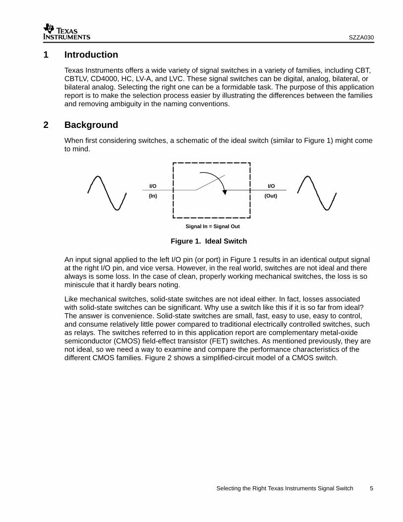
When first considering switches, a schematic of the ideal switch (similar to Figure 1) might cometo mind.
(In) (Out)
I/O I/O
Signal In = Signal Out
Figure 1. Ideal Switch
An input signal applied to the left I/O pin (or port) in Figure 1 results in an identical output signalat the right I/O pin, and vice versa. However, in the real world, switches are not ideal and therealways is some loss. In the case of clean, properly working mechanical switches, the loss is sominiscule that it hardly bears noting.
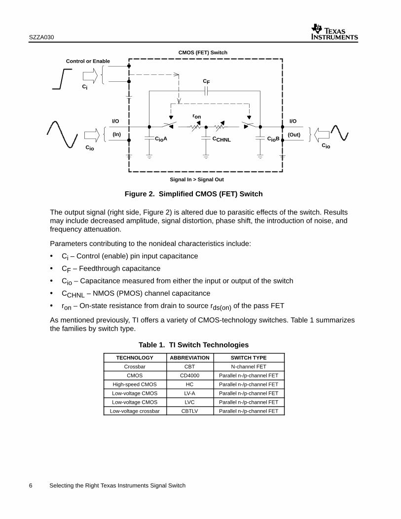
Like mechanical switches, solid-state switches are not ideal either. In fact, losses associatedwith solid-state switches can be significant. Why use a switch like this if it is so far from ideal?The answer is convenience. Solid-state switches are small, fast, easy to use, easy to control,and consume relatively little power compared to traditional electrically controlled switches, suchas relays. The switches referred to in this application report are complementary metal-oxidesemiconductor (CMOS) field-effect transistor (FET) switches. As mentioned previously, they arenot ideal, so we need a way to examine and compare the performance characteristics of thedifferent CMOS families. Figure 2 shows a simplified-circuit model of a CMOS switch.
SZZA030
6 Selecting the Right Texas Instruments Signal Switch
Ci
(In) (Out)
CMOS (FET) Switch
Control or Enable
I/OI/O
Signal In > Signal Out
CF
CioA CCHNL
ron
Cio
CioBCio
Figure 2. Simplified CMOS (FET) Switch
The output signal (right side, Figure 2) is altered due to parasitic effects of the switch. Resultsmay include decreased amplitude, signal distortion, phase shift, the introduction of noise, andfrequency attenuation.
Parameters contributing to the nonideal characteristics include:
• Ci – Control (enable) pin input capacitance
• CF – Feedthrough capacitance
• Cio – Capacitance measured from either the input or output of the switch
• CCHNL – NMOS (PMOS) channel capacitance
• ron – On-state resistance from drain to source rds(on) of the pass FET
As mentioned previously, TI offers a variety of CMOS-technology switches. Table 1 summarizesthe families by switch type.
Table 1. TI Switch Technologies
TECHNOLOGY ABBREVIATION SWITCH TYPE
Crossbar CBT N-channel FET
CMOS CD4000 Parallel n-/p-channel FET
High-speed CMOS HC Parallel n-/p-channel FET
Low-voltage CMOS LV-A Parallel n-/p-channel FET
Low-voltage CMOS LVC Parallel n-/p-channel FET
Low-voltage crossbar CBTLV Parallel n-/p-channel FET
SZZA030
7 Selecting the Right Texas Instruments Signal Switch
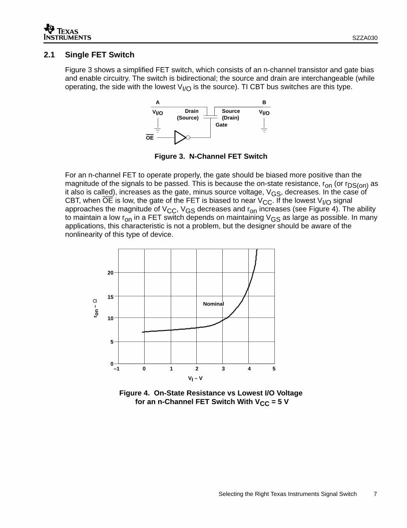
2.1 Single FET Switch
Figure 3 shows a simplified FET switch, which consists of an n-channel transistor and gate biasand enable circuitry. The switch is bidirectional; the source and drain are interchangeable (whileoperating, the side with the lowest VI/O is the source). TI CBT bus switches are this type.
Drain(Source)
Source(Drain)
OE
A B
Gate
VI/O VI/O
Figure 3. N-Channel FET Switch
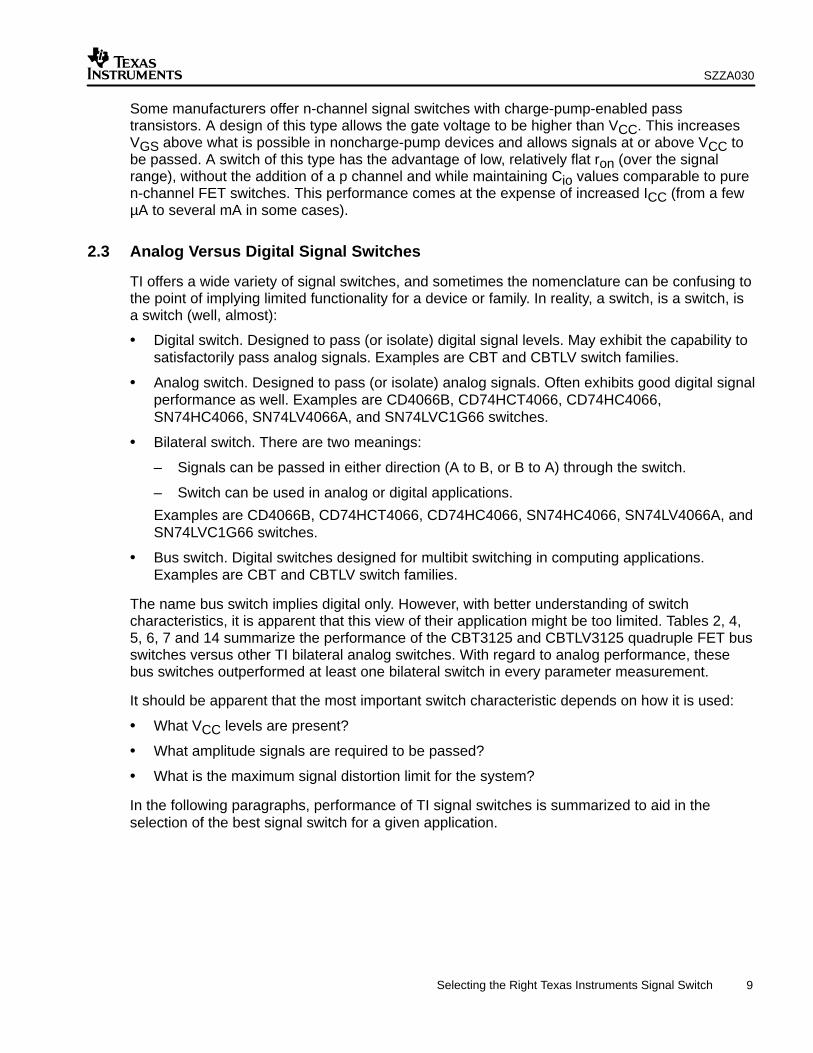
For an n-channel FET to operate properly, the gate should be biased more positive than themagnitude of the signals to be passed. This is because the on-state resistance, ron (or rDS(on) asit also is called), increases as the gate, minus source voltage, VGS, decreases. In the case ofCBT, when OE is low, the gate of the FET is biased to near VCC. If the lowest VI/O signalapproaches the magnitude of VCC, VGS decreases and ron increases (see Figure 4). The abilityto maintain a low ron in a FET switch depends on maintaining VGS as large as possible. In manyapplications, this characteristic is not a problem, but the designer should be aware of thenonlinearity of this type of device.
–1 0 1 2 3 4 5
5
10
15
20
VI – V
Nominal
r on
Ω
–
0
Figure 4. On-State Resistance vs Lowest I/O Voltage for an n-Channel FET Switch With VCC = 5 V

SZZA030
8 Selecting the Right Texas Instruments Signal Switch
2.2 Analog (Bilateral) Switches
Analog (or bilateral, as they also are called) switches consist of a single n-channel transistor inparallel with a single p-channel transistor (see Figure 5).
A
OE
B
VI/O VI/O
Figure 5. Parallel n-/p-Channel FET Switch
As before, when VI/O approaches VCC, the n-channel conductance decreases (ron increases)while the p-channel gate-source voltage is maximum and its ron is minimal. The resulting parallelresistance combination is much flatter than individual channel resistances (see Figure 6).
–1 0 1 2 3 4 5
5
10
15
20
VI – V
Nominal
p-Channel n-Channel
n-Channel || p-Channel
r on
Ω
–
0
Figure 6. On-State Resistance vs Input Voltage for a Parallel n-/p-Channel FET Switch
A flat ron is especially important if VI/O signals must swing from rail to rail. However, the tradeoffis increased switch capacitance due to the additional p-channel transistor and associated biascircuitry. TI offers a variety of choices of analog switches: HCT, HC, CD4000, LV-A, LVC, andCBTLV.
SZZA030
9 Selecting the Right Texas Instruments Signal Switch
Some manufacturers offer n-channel signal switches with charge-pump-enabled passtransistors. A design of this type allows the gate voltage to be higher than VCC. This increasesVGS above what is possible in noncharge-pump devices and allows signals at or above VCC tobe passed. A switch of this type has the advantage of low, relatively flat ron (over the signalrange), without the addition of a p channel and while maintaining Cio values comparable to puren-channel FET switches. This performance comes at the expense of increased ICC (from a fewµA to several mA in some cases).
2.3 Analog Versus Digital Signal Switches
TI offers a wide variety of signal switches, and sometimes the nomenclature can be confusing tothe point of implying limited functionality for a device or family. In reality, a switch, is a switch, isa switch (well, almost):
• Digital switch. Designed to pass (or isolate) digital signal levels. May exhibit the capability tosatisfactorily pass analog signals. Examples are CBT and CBTLV switch families.
• Analog switch. Designed to pass (or isolate) analog signals. Often exhibits good digital signalperformance as well. Examples are CD4066B, CD74HCT4066, CD74HC4066,SN74HC4066, SN74LV4066A, and SN74LVC1G66 switches.
• Bilateral switch. There are two meanings:
– Signals can be passed in either direction (A to B, or B to A) through the switch.
– Switch can be used in analog or digital applications.
Examples are CD4066B, CD74HCT4066, CD74HC4066, SN74HC4066, SN74LV4066A, andSN74LVC1G66 switches.
• Bus switch. Digital switches designed for multibit switching in computing applications.Examples are CBT and CBTLV switch families.
The name bus switch implies digital only. However, with better understanding of switchcharacteristics, it is apparent that this view of their application might be too limited. Tables 2, 4,5, 6, 7 and 14 summarize the performance of the CBT3125 and CBTLV3125 quadruple FET busswitches versus other TI bilateral analog switches. With regard to analog performance, thesebus switches outperformed at least one bilateral switch in every parameter measurement.
It should be apparent that the most important switch characteristic depends on how it is used:
• What VCC levels are present?
• What amplitude signals are required to be passed?
• What is the maximum signal distortion limit for the system?
In the following paragraphs, performance of TI signal switches is summarized to aid in theselection of the best signal switch for a given application.
SZZA030
10 Selecting the Right Texas Instruments Signal Switch
2.4 Application Considerations
2.4.1 Digital Signal Considerations
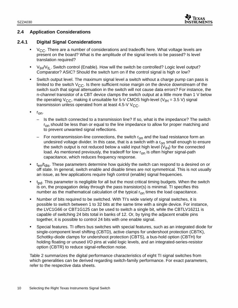
• VCC. There are a number of considerations and tradeoffs here. What voltage levels arepresent on the board? What is the amplitude of the signal levels to be passed? Is leveltranslation required?
• VIH/VIL. Switch control (Enable). How will the switch be controlled? Logic level output?Comparator? ASIC? Should the switch turn on if the control signal is high or low?
• Switch output level. The maximum signal level a switch without a charge pump can pass islimited to the switch VCC. Is there sufficient noise margin on the device downstream of theswitch such that signal attenuation in the switch will not cause data errors? For instance, then-channel transistor of a CBT device clamps the switch output at a little more than 1 V belowthe operating VCC, making it unsuitable for 5-V CMOS high-level (VIH = 3.5 V) signaltransmission unless operated from at least 4.5-V VCC.
• ron.
– Is the switch connected to a transmission line? If so, what is the impedance? The switchron should be less than or equal to the line impedance to allow for proper matching andto prevent unwanted signal reflections.
– For nontransmission-line connections, the switch ron and the load resistance form anundesired voltage divider. In this case, that is a switch with a ron small enough to ensurethe switch output is not reduced below a valid input high level (VIH) for the connectedload. As mentioned previously, the tradeoff for low ron is often higher signal-pathcapacitance, which reduces frequency response.
• ten/tdis. These parameters determine how quickly the switch can respond to a desired on oroff state. In general, switch enable and disable times are not symmetrical. This is not usuallyan issue, as few applications require high control (enable) signal frequencies.
• tpd. This parameter is negligible for all but the most critical timing budgets. When the switchis on, the propagation delay through the pass transistor(s) is minimal. TI specifies thisnumber as the mathematical calculation of the typical ron times the load capacitance.
• Number of bits required to be switched. With TI’s wide variety of signal switches, it ispossible to switch between 1 to 32 bits at the same time with a single device. For instance,the LVC1G66 or CBT1G125 can be used to switch a single bit, while the CBTLV16211 iscapable of switching 24 bits total in banks of 12. Or, by tying the adjacent enable pinstogether, it is possible to control 24 bits with one enable signal.
• Special features. TI offers bus switches with special features, such as an integrated diode forsingle-component level shifting (CBTD), active clamps for undershoot protection (CBTK),Schottky-diode clamps for undershoot protection (CBTS), a bus-hold option (CBTH) forholding floating or unused I/O pins at valid logic levels, and an integrated-series-resistoroption (CBTR) to reduce signal-reflection noise.
Table 2 summarizes the digital performance characteristics of eight TI signal switches fromwhich generalities can be derived regarding switch-family performance. For exact parameters,refer to the respective data sheets.
SZZA030
11 Selecting the Right Texas Instruments Signal Switch
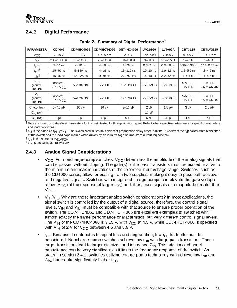
2.4.2 Digital Performance
Table 2. Summary of Digital Performance†
PARAMETER CD4066 CD74HC4066 CD74HCT4066 SN74HC4066 LVC1G66 LV4066A CBT3125 CBTLV3125
VCC 3–18 V 2–10 V 4.5–5.5 V 2–6 V 1.65–5.5V 2–5.5 V 4–5.5 V 2.3–3.6 V
ron 200–1300 Ω 15–142 Ω 25–142 Ω 30–150 Ω 3–30 Ω 21–225 Ω 5–22 Ω 5–40 Ω
tpd‡ 7–40 ns 4–90 ns 4–18 ns 3–75 ns 0.6–2 ns 0.3–18 ns 0.25–0.35ns 0.15–0.25 ns
ten§ 15–70 ns 8–150 ns 4–18 ns 18–225 ns 1.5–10 ns 1.6–32 ns 1.8–5.6 ns 2–4.6 ns
tdis¶ 15–70 ns 12–225 ns 9–36 ns 22–250 ns 1.4–10 ns 3.2–32 ns 1–4.6 ns 1–4.2 ns
VIH(controlinputs)
approx. 0.7 × VCC
5-V CMOS 5-V TTL 5-V CMOS 5-V CMOS 5-V CMOS5-V TTL/LVTTL
LVTTL/2.5-V CMOS
VIL(controlinputs)
approx. 0.2 × VCC
5-V CMOS 5-V TTL 5-V CMOS 5-V CMOS 5-V CMOS5-V TTL/LVTTL
LVTTL/2.5-V CMOS
Ci (control) 5–7.5 pF 10 pF 10 pF 3–10 pF 2 pF 1.5 pF 3 pF 2.5 pF
Cio (on) 13 pF
Cio (off) 8 pF 5 pF 5 pF 9 pF 6 pF 5.5 pF 4 pF 7 pF
† Data are based on data-sheet parameters for the parts tested for this application report. Refer to the respective data sheets for specific parametersand load conditions.
‡ tpd is the same as tPLH/tPHL. The switch contributes no significant propagation delay other than the RC delay of the typical on-state resistanceof the switch and the load capacitance when driven by an ideal voltage source (zero output impedance)
§ ten is the same as tPZL/tPZH.¶ tdis is the same as tPLZ/tPHZ.
2.4.3 Analog Signal Considerations
• VCC. For noncharge-pump switches, VCC determines the amplitude of the analog signals thatcan be passed without clipping. The gate(s) of the pass transistors must be biased relative tothe minimum and maximum values of the expected input voltage range. Switches, such asthe CD4000 series, allow for biasing from two supplies, making it easy to pass both positiveand negative signals. Switches with integrated charge pumps can elevate the gate voltageabove VCC (at the expense of larger ICC) and, thus, pass signals of a magnitude greater thanVCC.
• VIH/VIL. Why are these important analog switch considerations? In most applications, thesignal switch is controlled by the output of a digital source, therefore, the control signallevels, VIH and VIL, must be compatible with that source to ensure proper operation of theswitch. The CD74HC4066 and CD74HCT4066 are excellent examples of switches withalmost exactly the same performance characteristics, but very different control signal levels.The VIH of the CD74HC4066 is 3.15 V, with VCC at 4.5 V, while CD74HCT4066 is specifiedwith VIH of 2 V for VCC between 4.5 and 5.5 V.
• ron. Because it contributes to signal loss and degradation, low ron tradeoffs must beconsidered. Noncharge-pump switches achieve low ron with large pass transistors. Theselarger transistors lead to larger die sizes and increased Cio. This additional channelcapacitance can be very significant as it limits the frequency response of the switch. Asstated in section 2.4.1, switches utilizing charge-pump technology can achieve low ron andCio, but require significantly higher ICC.

SZZA030
12 Selecting the Right Texas Instruments Signal Switch
• Frequency response. All CMOS switches have an upper limit to the frequency that can bepassed. No matter how low ron and Cio can be maintained in the chip manufacturing process,they still form an undesired low-pass filter that attenuates the switch output signal.
• Sine-wave distortion or total harmonic distortion. These are measurements of the linearity ofthe device. Nonlinearity can be introduced a number of ways (design, device physics, etc.)but, typically, the largest contributor is ron. As shown in Figures 2 and 4, ron varies with VI/Ofor all types of CMOS switches. Having a low ron is important, but a flat ron over the signalrange is almost equally important. N-channel switches, such as CBT, exhibit very flat roncharacteristics for signal ranges of 0 < VI/O < (VCC – 2 V), but ron increases very rapidly asVI/O approaches VCC and VGS decreases. Parallel n-/p-channel switches offer good ronflatness for signal ranges of 0 < VI/O < VCC, with the best flatness characteristic at thehighest recommended switch VCC.
• Crosstalk. There are two types of crosstalk to consider:
– Control (enable) to output. The level of crosstalk is a measure of how well decoupled theswitch control signal is from the switch output. Due to the parasitic capacitance of CMOSprocesses, changing the state on the control signal causes noise to appear on theoutput. In audio applications, this can be a source of the annoying pop that is sometimesheard when switching the unit on or off.
– Between switches. The level of crosstalk also is a measure of adjacent-channel rejection.As with control-to-output crosstalk, parasitic capacitance can couple the signal on oneswitch with that on another switch.
• Charge Injection (Q). TI specifies enable-to-output crosstalk and some competitors use thisparameter. As with enable-to-output crosstalk, changing the state on the control pin causes acharge to be coupled to the channel of the transistor introducing signal noise. It is presentedin this report for a relative comparison with the competition.
• Feedthrough. This characteristic is related to the ability of the switch to block signals whenoff. As with crosstalk, parasitic capacitance allows high frequencies to couple through theswitch, making it appear to be on.

SZZA030
13 Selecting the Right Texas Instruments Signal Switch
2.4.4 Analog Performance
Table 3. VCC Above 5.5 V†
PARAMETER BETTER PERFORMANCE
ron(typical to maximum)
CD74HC406615–126 Ω
CD74HC4066‡
30 ΩCD4066
200–550 Ω
ron (peak)(typical to maximum)
SN74HC4066‡
50 Ω (typ)CD74HC4066not specified
CD4066not specified
Frequency response CD74HC4066§ CD4066 SN74HC4066§Frequency response
200 MHz 40 MHz 30 MHz
THD/Sine wave distortion CD74HC4066 SN74HC4066§ CD4066THD/Sine-wave distortion
0.008% 0.05% 0.4%
Crosstalk SN74HC4066 CD4066 CD74HC4066(enable to output) 20 mV 50 mV 550 mV
Crosstalk CD4066 CD74HC4066§ SN74HC4066§
(between switches) –50 dB at 8 MHz –72 dB at 1 MHz –45 dB at 1 MHz
Feedthrough attenuation CD74HC4066§ CD4066 SN74HC4066§Feedthrough attenuation
–72 dB at 1 MHz –50 dB at 1 MHz –42 dB at 1 MHz
† Data are based on data-sheet parameters for the parts tested for this application report. Refer to the respective data sheets forspecific parameters and load conditions.
‡ Specification at VCC = 6 V§ Specification at VCC = 4.5 V
Table 4. VCC = 4.5 V†
PARAMETER BETTER PERFORMANCE
ron LVC1G66 CBT3125‡ LV4066ACD74HC/HCT4066
SN74HC4066 CBT3125§on(typical to maximum) 3–10 Ω 5–15 Ω 21–100 Ω HCT4066
25–142 Ω 50–106 Ω 5–1000 Ω
ron (peak)(typical to maximum)
CBT3125‡§
10 ΩLVC1G666–15 Ω
LV4066A31–125 Ω
CD74HC/HCT4066§
50–70 Ω
SN74HC406670–215 Ω
CBT3125§
1000 Ω
Frequency responseCBT3125‡§
>200 MHzLVC1G66195 MHz
CD74HC/HCT4066¶
200 MHz
LV4066A50 MHz
SN74HC406630 MHz
THD/Sine wave distortionLVC1G66
CD74HC/HCT4066
CBT3125ठSN74HC4066 LV4066ATHD/Sine-wave distortion
0.01%HCT40660.023%
0.035% 0.05% 0.1%
Crosstalk(enable to output)
SN74HC406615 mV
LV4066A50 mV
LVC1G66100 mV
CBT3125§
120 mVCD74HCT4066
130 mVCD74HC4066
200 mV
Crosstalk(between switches)
CD74HC/HCT4066–72 dB
LVC2G66–58 dB
CBT3125‡§
–53 dBSN74HC4066
–45 dBLV4066A–45 dB
Feedthrough attenuationCD74HC/HCT4066
–72 dBLVC1G66
–58 dBSN74HC4066
–42 dBLV4066A–40 dB
CBT3125§
–36 dB† Data are based on data-sheet parameters for the parts tested for this application report. Refer to the respective data sheets for specific parameters
and load conditions.‡ CBT3125, 0 ≤ VI/O ≤ (VCC – 2 V)§ Value from application report measurement. Not specified in data sheet.¶ Ranked here due to load variation from other devices in this report

SZZA030
14 Selecting the Right Texas Instruments Signal Switch
Table 5. VCC = 3 V†
PARAMETER BETTER PERFORMANCE
ron(typical to maximum)
LVC1G666–15 Ω
CBTLV31255–15 Ω
LV4066A29–190 Ω
CD74HC4066‡
Not specifiedSN74HC4066‡
Not specified
ron (peak)(typical to maximum)
CBTLV3125§
15–20 ΩLVC1G6612–20 Ω
LV4066A57–225 Ω
CD74HC4066‡
Not specifiedSN74HC4066‡
Not specified
Frequency responseCBTLV3125§
>200 MHzLVC1G66175 MHz
CD74HC4066‡
Not specifiedLV4066A35MHz
SN74HC4066†
Not specified
THD/Sine-wave distortionLVC1G660.015%
CD74HC4066‡
Not specifiedSN74HC4066‡
Not specifiedCBTLV3125§
0.09%LV4066A
0.1%
Crosstalk(enable to output)
SN74HC4066‡
Not specifiedLV4066A
20 mVLVC1G66
70 mVCBTLV3125§
70 mVCD74HC4066‡
Not specified
Crosstalk(between switches)
CD74HC4066‡
Not specifiedLVC2G66
–58 dBCBTLV3125§
–49 dBSN74HC4066‡
Not specifiedLV4066A–45 dB
Feedthrough attenuationCD74HC4066‡
Not specifiedLVC1G66
–58 dBCBTLV3125
–52 dBSN74HC4066‡
Not specifiedLV4066A–40 dB
† Data are based on data-sheet parameters for the parts tested for this application report. Refer to the respective data sheets for specific parametersand load conditions.
‡ Position in table based on estimated performance. Information not specified in data sheet.§ Value from application report measurement. Not specified in data sheet.
Table 6. VCC = 2.5 V†
PARAMETER BETTER PERFORMANCE
ron(typical to maximum)
LVC1G669–20 Ω
CBTLV31255–40 Ω
LV4066A38–225 Ω
CD74HC4066‡
Not specifiedSN74HC4066§
150 Ω
ron (peak)(typical to maximum)
CBTLV3125¶
15–45 ΩLVC1G6620–30 Ω
LV4066A143–600 Ω
CD74HC4066‡
Not specifiedSN74HC4066§
320 Ω
Frequency responseCBTLV3125¶
>200 MHzLVC1G66120 MHz
CD74HC4066‡
Not specifiedLV4066A30 MHz
SN74HC4066‡
Not specified
THD/Sine-wave distortionLVC1G660.025%
CD74HC4066‡
Not specifiedSN74HC4066‡
Not specifiedLV4066A
0.1%CBTLV3125¶
0.11%
Crosstalk(enable to output)
SN74HC4066‡
Not specifiedLV4066A
15 mVCBTLV3125‡
30 mVLVC1G66
50 mVCD74HC4066‡
Not specified
Crosstalk(between switches)
CD74HC4066‡
Not specifiedLVC2G66
–58 dBCBTLV3125
–45 dBSN74HC4066‡
Not specifiedLV4066A–45 dB
Feedthrough attenuationCD74HC4066‡
Not specifiedLVC1G66
–58 dBCBTLV3125
–52 dBSN74HC4066‡
Not specifiedLV4066A–40 dB
† Data are based on data-sheet parameters for the parts tested for this application report. Refer to the respective data sheets for specific parametersand load conditions.
‡ Position in table based on estimated performance. Information not specified in data sheet.§ Data at VCC = 2 V¶ Value from application report measurement. Not specified in data sheet.

SZZA030
15 Selecting the Right Texas Instruments Signal Switch
2.4.5 SN74CBT Characteristics
–40°C
VI
1
10
100
1000
10000
0 1 2 3 4 5
r on
25°C
85°C
Figure 7. Log ron vs VI, VCC = 5 V (SN74CBT3125)
VI
0
5
10
15
20
25
30
0 0.5 1.5 2 2.5 3 3.5 41
r on
25°C
85°C
–40°C
Figure 8. ron vs VI, VCC = 5 V (SN74CBT3125)
SZZA030
16 Selecting the Right Texas Instruments Signal Switch
–40°C
25°C
85°C
VI
0
0.5
1
1.5
2
2.5
3
3.5
4
4.5
0 1 2 3 4 5
VO
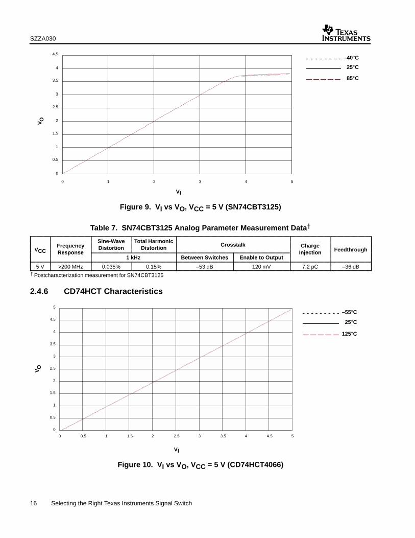
Figure 9. VI vs VO, VCC = 5 V (SN74CBT3125)
Table 7. SN74CBT3125 Analog Parameter Measurement Data†
VCCFrequencyResponse
Sine-WaveDistortion
Total HarmonicDistortion Crosstalk Charge
Injection FeedthroughCC Response1 kHz Between Switches Enable to Output
Injection g
5 V >200 MHz 0.035% 0.15% –53 dB 120 mV 7.2 pC –36 dB† Postcharacterization measurement for SN74CBT3125
2.4.6 CD74HCT Characteristics
–55°C
25°C
125°C
VI
0
0.5
1
1.5
2
2.5
3
3.5
4
4.5
5
0 0.5 1 1.5 2 2.5 3 3.5 4 4.5 5
VO
Figure 10. VI vs VO, VCC = 5 V (CD74HCT4066)

SZZA030
17 Selecting the Right Texas Instruments Signal Switch
–55°C
25°C
125°C
VI
0
10
20
30
40
50
60
70
80
0 0.5 1 1.5 2 2.5 3 3.5 4 4.5 5
r on
Figure 11. ron vs VI, VCC = 5 V (CD74HCT4066)
Table 8. CD74HCT4066 Analog Parameter Measurement Data†
VCCFrequencyResponse
Total HarmonicDistortion Crosstalk
Charge Injection‡ FeedthroughCC Response1 kHz Between Switches Enable to Output
g j g
4.5 V 200 MHz 0.023% –72 dB 130 mV 8.1 pC –72 dB† Data-sheet values for CD74HCT4066, except as noted‡ Postcharacterization measurement for CD74HCT4066
SZZA030
18 Selecting the Right Texas Instruments Signal Switch
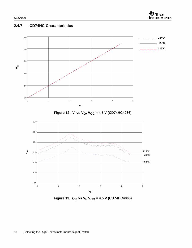
2.4.7 CD74HC Characteristics
VI
0.0
1.0
2.0
3.0
4.0
0 1 2 3 4 5
5.0 –55°C
25°C
125°C
VO
Figure 12. VI vs VO, VCC = 4.5 V (CD74HC4066)
VI
0.0
10.0
20.0
30.0
40.0
50.0
60.0
0 1 2 3 4 5
r on 125°C
–55°C
25°C
Figure 13. ron vs VI, VCC = 4.5 V (CD74HC4066)
SZZA030
19 Selecting the Right Texas Instruments Signal Switch
–55°C
25°C
125°C
VI
0.0
1.0
2.0
3.0
4.0
5.0
6.0
0 1 2 3 4 5 6
VO
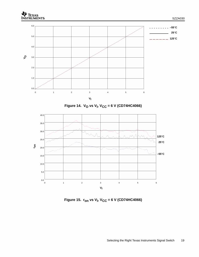
Figure 14. VO vs VI, VCC = 6 V (CD74HC4066)
VI
0.0
5.0
10.0
15.0
20.0
25.0
30.0
35.0
40.0
0 1 2 3 4 5 6
r on
–55°C
25°C
125°C
Figure 15. ron vs VI, VCC = 6 V (CD74HC4066)

SZZA030
20 Selecting the Right Texas Instruments Signal Switch
VI
–55°C
25°C
125°C
0.0
1.0
2.0
3.0
4.0
5.0
6.0
7.0
8.0
9.0
0 1 2 3 4 5 6 7 8 9
VO
Figure 16. VO vs VI, VCC = 9 V (CD74HC4066)
VI
0.0
5.0
10.0
15.0
20.0
25.0
30.0
0 1 2 3 4 5 6 7 8 9
r on
–55°C
25°C
125°C
Figure 17. ron vs VI, VCC = 9 V (CD74HC4066)
Table 9. CD74HC4066 Analog Parameter Measurement Data†
VCCFrequency Total Harmonic Distortion Crosstalk
Charge Injection‡ Feedthro ghVCCq y
Response 1 kHz Between Switches Enable to OutputCharge Injection‡ Feedthrough
4.5 V 200 MHz 0.022% –72 dB 200 mV 6.2 pC –72 dB
9 V 200 MHz 0.008% N/A 550 mV 9.0 pC N/A† Data-sheet values for CD74HC4066, except as noted‡ Postcharacterization measurement for CD74HC4066

SZZA030
21 Selecting the Right Texas Instruments Signal Switch
2.4.8 SN74HC Characteristics
VI
–40°C
25°C
85°C
0
0.2
0.4
0.6
0.8
1
1.2
1.4
1.6
1.8
2
0 0.5 1 1.5 2
VO
Figure 18. VO vs VI, VCC = 2 V (SN74HC4066)
VI
0
50
100
150
200
250
300
350
0 0.5 1 1.5 2
r on
–40°C 25°C
85°C
Figure 19. ron vs VI, VCC = 2 V (SN74HC4066)

SZZA030
22 Selecting the Right Texas Instruments Signal Switch
VI
–40°C
25°C
85°C
0
1
2
3
4
5
0 1 2 3 4 5
VO
Figure 20. VO vs VI, VCC = 4.5 V (SN74HC4066)
VI
0
10
20
30
40
50
60
70
80
0 0.5 1 1.5 2 2.5 3 3.5 4 4.5
r on
–40°C
25°C
85°C
Figure 21. ron vs VI, VCC = 4.5 V (SN74HC4066)
SZZA030
23 Selecting the Right Texas Instruments Signal Switch
VI
–40°C
25°C
85°C
0
1
2
3
4
5
6
7
0 1 2 3 4 5 6
VO
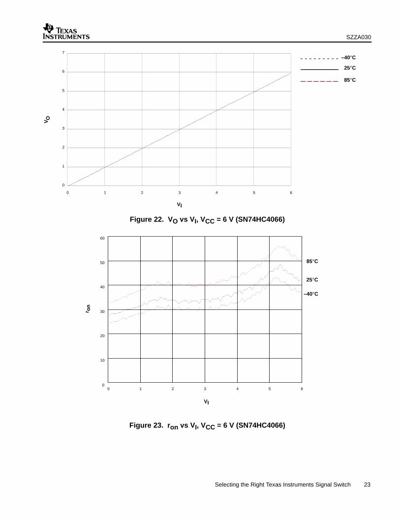
Figure 22. VO vs VI, VCC = 6 V (SN74HC4066)
VI
0
10
20
30
40
50
60
0 1 2 3 4 5 6
r on
–40°C
25°C
85°C
Figure 23. ron vs VI, VCC = 6 V (SN74HC4066)

SZZA030
24 Selecting the Right Texas Instruments Signal Switch
Table 10. SN74HC4066 Analog Parameter Measurement Data†
VCCFrequency Sine-Wave Distortion Crosstalk
Charge Injection‡ Feedthro ghVCCq y
Response 1 kHz Between Switches Enable to OutputCharge Injection‡ Feedthrough
2 V N/A N/A N/A N/A 3.8 pC N/A
4.5 V 30 MHz 0.05% –45 dB 15 mV 5.9 pC –42 dB
6 V N/A N/A N/A 20 mV 7.9 pC N/A† Data-sheet values for SN74HC4066, except as noted‡ Postcharacterization measurement for SN74HC4066
2.4.9 CD4066B Characteristics
VI
0
0.5
1
1.5
2
2.5
3
3.5
4
4.5
5
0 1 2 3 4 5
VO
–55°C
25°C
125°C
Figure 24. VO vs VI, VCC = 5 V (CD4066B)

SZZA030
25 Selecting the Right Texas Instruments Signal Switch
VI
0
100
200
300
400
500
600
0 1 2 3 4 5
r on
–55°C
25°C
125°C
Figure 25. ron vs VI, VCC = 5 V (CD4066B)
VI
0
1
2
3
4
5
6
7
8
9
10
0 2 4 6 8 10
VO
–55°C
25°C
125°C
Figure 26. VO vs VI, VCC = 10 V (CD4066B)

SZZA030
26 Selecting the Right Texas Instruments Signal Switch
VI
0
50
100
150
200
250
300
0 2 4 6 8 10
r on
–55°C
25°C
125°C
Figure 27. ron vs VI, VCC = 10 V (CD4066B)
VI
0
2
4
6
8
10
12
14
16
0 2 4 6 8 10 12 14 16
VO
–55°C
25°C
125°C
Figure 28. VO vs VI, VCC = 15 V (CD4066B)
SZZA030
27 Selecting the Right Texas Instruments Signal Switch
VI
0
20
40
60
80
100
120
140
160
180
200
0 2 4 6 8 10 12 14 16
r on
–55°C
25°C
125°C
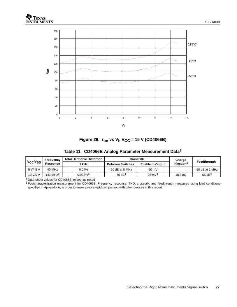
Figure 29. ron vs VI, VCC = 15 V (CD4066B)
Table 11. CD4066B Analog Parameter Measurement Data†
VCC/VSSFrequency Total Harmonic Distortion Crosstalk Charge
Feedthro ghVCC/VSSq y
Response 1 kHz Between Switches Enable to Outputg
Injection‡ Feedthrough
5 V/–5 V 40 MHz 0.04% –50 dB at 8 MHz 50 mV –50 dB at 1 MHz
10 V/0 V 141 MHz‡ 0.032%‡ –75 dB‡ 35 mV‡ 18.8 pC –65 dB‡
† Data-sheet values for CD4066B, except as noted‡ Postcharacterization measurement for CD4066B. Frequency response, THD, crosstalk, and feedthrough measured using load conditions
specified in Appendix A, in order to make a more valid comparison with other devices in this report.

SZZA030
28 Selecting the Right Texas Instruments Signal Switch
2.4.10 LV-A Characteristics
VI
0
0.5
1
1.5
2
2.5
0 0.5 1 1.5 2
VO
–40°C
25°C
85°C
Figure 30. VO vs VI, VCC = 2 V (SN74LV4066A)
VI
0
50
100
150
200
250
300
350
400
0 0.5 1 1.5 2 2.5
r on
25°C
–40°C
85°C
Figure 31. ron vs VI, VCC = 2 V (SN74LV4066A)
SZZA030
29 Selecting the Right Texas Instruments Signal Switch
VI
0
0.5
1
1.5
2
2.5
3
0 0.5 1 1.5 2 2.5 3
VO
–40°C
25°C
85°C
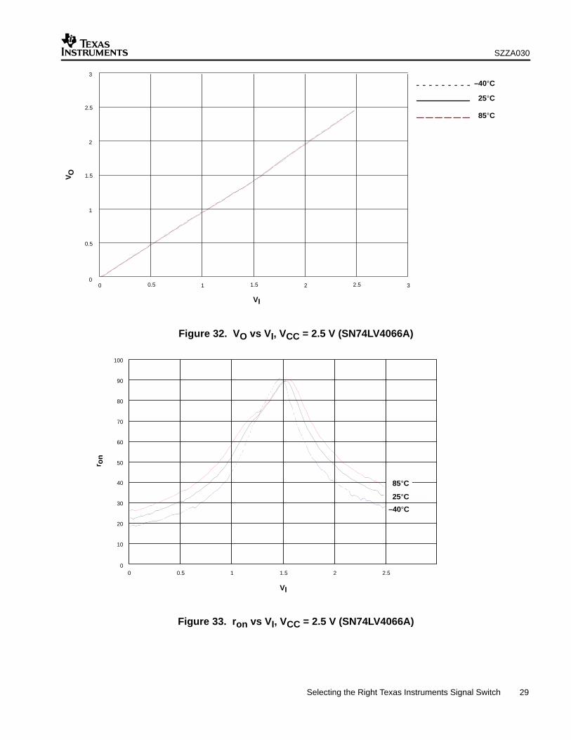
Figure 32. VO vs VI, VCC = 2.5 V (SN74LV4066A)
VI
0
10
20
30
40
50
60
70
80
90
100
0 0.5 1 1.5 2 2.5
r on
–40°C
25°C
85°C
Figure 33. ron vs VI, VCC = 2.5 V (SN74LV4066A)
SZZA030
30 Selecting the Right Texas Instruments Signal Switch
VI
0
0.5
1
1.5
2
2.5
3
3.5
0 0.5 1 1.5 2 2.5 3 3.5
VO
–40°C
25°C
85°C
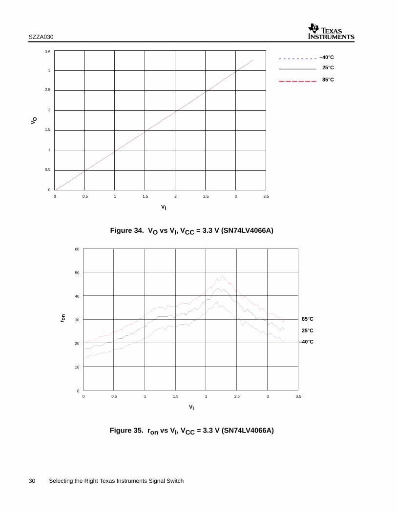
Figure 34. VO vs VI, VCC = 3.3 V (SN74LV4066A)
VI
0
10
20
30
40
50
60
0 0.5 1 1.5 2 2.5 3 3.5
r on
–40°C
25°C
85°C
Figure 35. ron vs VI, VCC = 3.3 V (SN74LV4066A)

SZZA030
31 Selecting the Right Texas Instruments Signal Switch
VI
0
1
2
3
4
5
0 1 2 3 4 5
VO
–40°C
25°C
85°C
Figure 36. VO vs VI, VCC = 5 V (SN74LV4066A)
VI
0
5
10
15
20
25
30
0 1 2 3 4 5
r on –40°C
25°C
85°C
Figure 37. ron vs VI, VCC = 5 V (SN74LV4066A)
SZZA030
32 Selecting the Right Texas Instruments Signal Switch
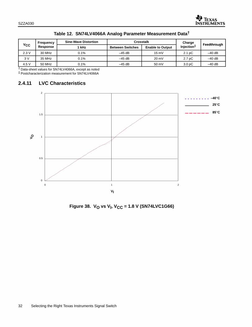
Table 12. SN74LV4066A Analog Parameter Measurement Data†
VCCFrequency Sine-Wave Distortion Crosstalk Charge
Feedthro ghVCCq y
Response 1 kHz Between Switches Enable to Outputg
Injection‡ Feedthrough
2.3 V 30 MHz 0.1% –45 dB 15 mV 2.1 pC –40 dB
3 V 35 MHz 0.1% –45 dB 20 mV 2.7 pC –40 dB
4.5 V 50 MHz 0.1% –45 dB 50 mV 3.0 pC –40 dB† Data-sheet values for SN74LV4066A, except as noted‡ Postcharacterization measurement for SN74LV4066A
2.4.11 LVC Characteristics
VI
0
0.5
1
1.5
2
0 1 2
VO
–40°C
25°C
85°C
Figure 38. VO vs VI, VCC = 1.8 V (SN74LVC1G66)
SZZA030
33 Selecting the Right Texas Instruments Signal Switch
VI
10
30
50
70
90
110
0 1 2
r on
25°C
–40°C
85°C
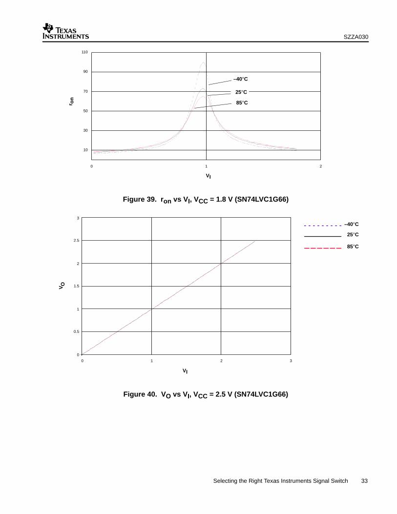
Figure 39. ron vs VI, VCC = 1.8 V (SN74LVC1G66)
VI
0
0.5
1
1.5
2
2.5
3
0 1 2 3
VO
–40°C
25°C
85°C
Figure 40. VO vs VI, VCC = 2.5 V (SN74LVC1G66)

SZZA030
34 Selecting the Right Texas Instruments Signal Switch
VI
0
5
10
15
20
0 1 2 3
r on
25°C
85°C
–40°C
Figure 41. ron vs VI, VCC = 2.5 V (SN74LVC1G66)
VI
0
0.5
1
1.5
2
2.5
3
0 1 2 3
VO
–40°C
25°C
85°C
Figure 42. VO vs VI, VCC = 3.3 V (SN74LVC1G66)

SZZA030
35 Selecting the Right Texas Instruments Signal Switch
VI
0
5
10
15
0 2 4
r on 25°C
85°C
–40°C
Figure 43. ron vs VI, VCC = 3.3 V (SN74LVC1G66)
VI
0
1
2
3
4
5
6
0 1 2 3 4 5 6
VO
–40°C
25°C
85°C
Figure 44. VO vs VI, VCC = 5 V (SN74LVC1G66)

SZZA030
36 Selecting the Right Texas Instruments Signal Switch
VI
0
1
2
3
4
5
6
7
8
0 1 2 3 4 5
r on
25°C
85°C
–40°C
Figure 45. ron vs VI, VCC = 5 V (SN74LVC1G66)
Table 13. SN74LVC1G66 Analog Parameter Measurement Data†
VCCFrequency Sine-Wave Distortion Crosstalk Charge
Feedthro ghVCCq y
Response 1 kHz 10 kHz Enable to Outputg
Injection‡ Feedthrough
1.8 V 35 MHz 0.1% 0.15% 35 mV 2.5 pC –42 dB
2.5 V 120 MHz 0.025% 0.025% 50 mV 3.0 pC –42 dB
3 V 175 MHz 0.015% 0.015% 70 mV 3.3 pC –42 dB
4.5 V 195 MHz 0.01% 0.01% 100 mV 3.5 pC –42 dB† Data-sheet values for SN74LVC1G66, except as noted‡ Postcharacterization measurement for SN74LVC1G66

SZZA030
37 Selecting the Right Texas Instruments Signal Switch
2.4.12 CBTLV Characteristics
VI
0
1
2
3
0 1 2 3
VO
–40°C
25°C
85°C
Figure 46. VO vs VI, VCC = 2.5 V (SN74CBTLV3125)
VI
0
2
4
6
8
10
12
0 0.5 1 1.5 2 2.5 3
r on
85°C
–40°C
25°C
Figure 47. ron vs VI, VCC = 2.5 V (SN74 CBTLV3125)

SZZA030
38 Selecting the Right Texas Instruments Signal Switch
VI
0
1
2
3
0 1 2 3 4
4
VO
–40°C
25°C
85°C
Figure 48. VO vs VI, VCC = 3.3 V (SN74CBTLV3125)
VI
0
1
2
3
4
5
6
7
8
9
10
0 1 2 3 4
r on
25°C
85°C
–40°C
Figure 49. ron vs VI, VCC = 3.3 V (SN74CBTLV3125)

SZZA030
39 Selecting the Right Texas Instruments Signal Switch
Table 14. SN74CBTLV3125 Analog Parameter Measurement Data†
VCCFrequencyResponse
Sine-WaveDistortion
TotalHarmonicDistortion
Crosstalk ChargeInjection Feedthroughp
1 kHz 1 kHz Between Switches Enable to Output
j
2.5 V >200 MHz 0.089% 0.11% –45 dB 30 mV 12.1 pC –52 dB
3.3 V >200 MHz 0.033% 0.09% –49 dB 70 mV 15.5 pC –52 dB† Postcharacterization measurement for CBTLV3125

SZZA030
40 Selecting the Right Texas Instruments Signal Switch
3 Applications
TI signal switches can be configured for numerous applications. Three switches are presentedhere for illustrative purposes:
• A bus switch in an analog application (digital switch in an analog application)
• Improvement of off-isolation characteristics with a T configuration
• Single-bit level shifting with an analog switch (analog switch in a digital application)
3.1 CBT3125 as a Gain-Control Circuit [for VI < (VCC – 2 V)] With LMV321
An example of the CBT3125 in a gain-control circuit is shown in Figure 50.
CBT3125
1IN+
GND
IN– OUT
LMV321
–
+
–
+
1A
2A
3A
1B
2B
3B
4A 4B
LMV321
VCC4OE
4A
4B
3OE
3A
3B
1OE1A1B2OE2A2BGND
VIVO
R1
R2
R3
R4
R5
ron(1)
ron(3)
ron(2)
ron(4)
VOVI
1 R
R5
R R1 ron(1) R2 ron(2)
R3 ron(3) R4 ron(4)
VCC
R1
R2
R3
R4
R5
VI VO
VCC+
+ +
Figure 50. CBT3125 Gain-Control Circuit
By choosing values for R1 through R4, such that RX >> ron(x), the on-state resistance of theCBT3125 can be ignored. Thus, RII simplifies to:
RII = R1 II R2 II R3 II R4
Because the CBT device uses 5-V TTL switching levels, it can be controlled easily from eitherCMOS or TT logic.

SZZA030
41 Selecting the Right Texas Instruments Signal Switch
3.2 LVC4066A T-Switch
The series connection doubles the effective switch ron when passing signals, but the tradeoff isimproved off isolation—a key concern when passing high-frequency signals. Feedthroughattenuation for the LV4066A is specified as –40 dB using a single switch. However, whenconnected in a T configuration as shown in Figure 51, isolation in excess of –65 dB wasmeasured using a 5-V VCC.
C Switch PositionL 1, 2 open; 3 closedH 1, 2 closed; 3 open
1B1B
1 2
3
IN
OUT LVC3G04
C
R
C
C
1A
3Y2AGND
1Y3A2Y
1A
3Y2AGND
1Y3A2Y
1A
3Y2AGND
1Y3A2Y
T-Switch
CF(2)CF(1)
ron(1) ron(2)
ron(3)
VI VO
CF(3)
LV4066A
1A
2B
2A
2C
1C
4C
4A
4B
1A
2B
2A
2C
1C
4C
4A
4B
1A
2B
2A
2C
4C
4A
4B
3C3C3C
GND
3B
3AGND
3B
3AGND
3B
3A
1B
VCC
VCC
Figure 51. LV4066A/LVC2G04 T-Switch Configuration
The values of R and C (including PCB resistance and capacitance) are chosen such that theR || ron(4) × C time constant is faster than the propagation delay through the inverter. This allowsswitch 3 to open before switches 1 and 2 close. Conversely, the R × C time constant slows thetransition of the control signal to switch 3, allowing switches 1 and 2 to open before switch 3closes.
SZZA030
42 Selecting the Right Texas Instruments Signal Switch
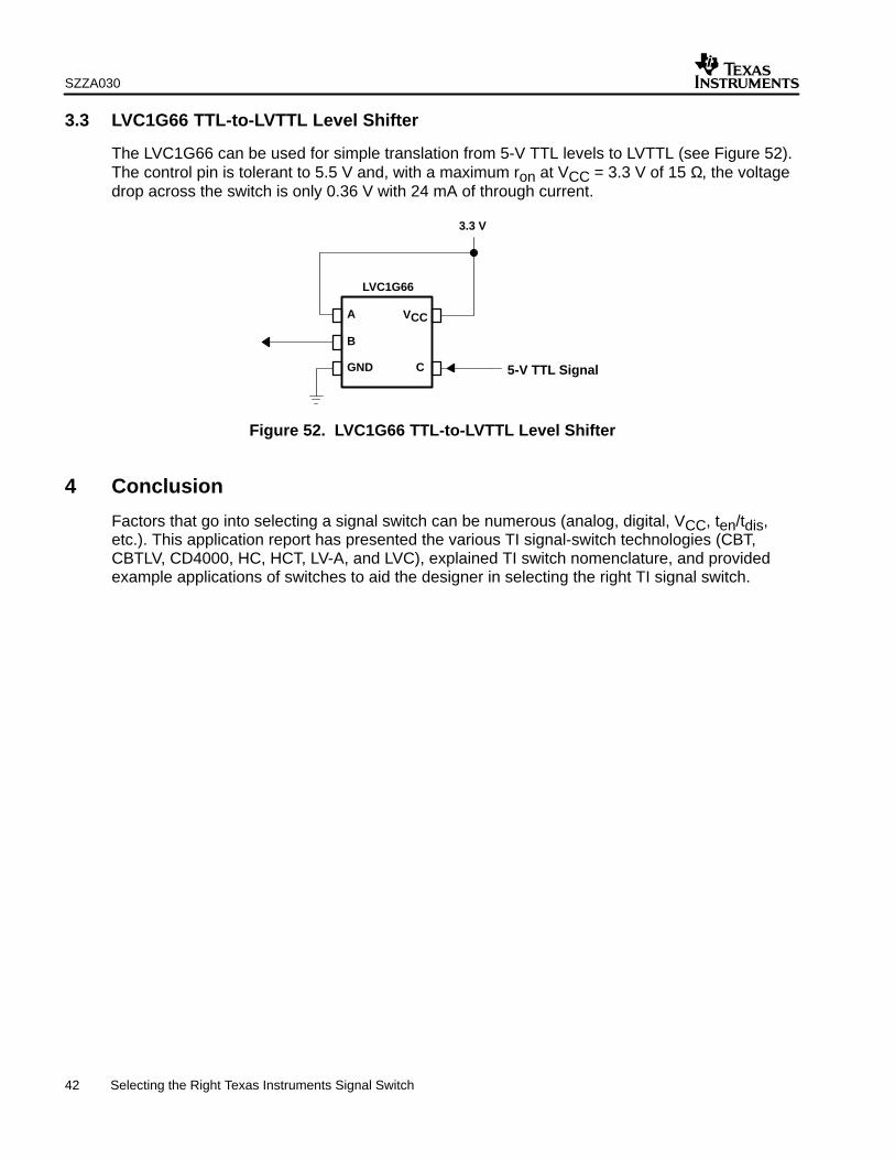
3.3 LVC1G66 TTL-to-LVTTL Level Shifter
The LVC1G66 can be used for simple translation from 5-V TTL levels to LVTTL (see Figure 52).The control pin is tolerant to 5.5 V and, with a maximum ron at VCC = 3.3 V of 15 Ω, the voltagedrop across the switch is only 0.36 V with 24 mA of through current.
LVC1G66
5-V TTL Signal
3.3 V
A
B
GND C
VCC
Figure 52. LVC1G66 TTL-to-LVTTL Level Shifter
4 Conclusion
Factors that go into selecting a signal switch can be numerous (analog, digital, VCC, ten/tdis,etc.). This application report has presented the various TI signal-switch technologies (CBT,CBTLV, CD4000, HC, HCT, LV-A, and LVC), explained TI switch nomenclature, and providedexample applications of switches to aid the designer in selecting the right TI signal switch.
SZZA030
43 Selecting the Right Texas Instruments Signal Switch
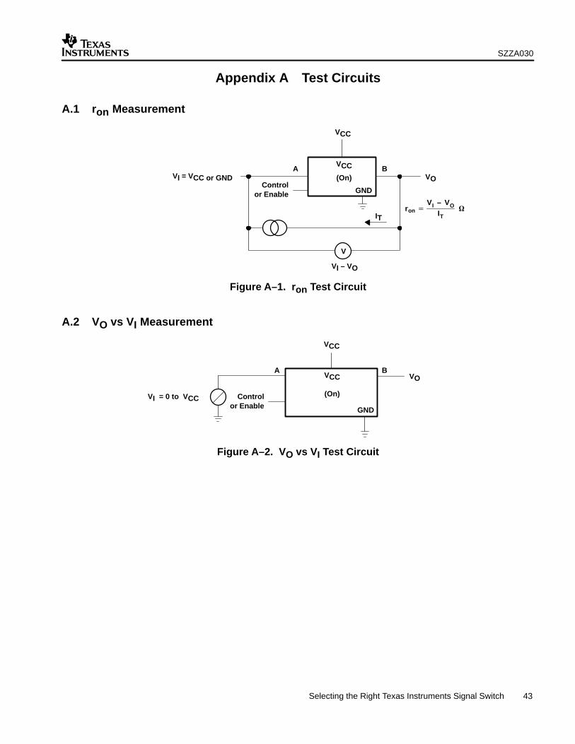
Appendix A Test Circuits
A.1 ron Measurement
VCC
VI = VCC or GND
IT
VO
ronVI – VO
IT
VI – VO
VCC
GND
(On)A
V
B
Controlor Enable
Figure A–1. ron Test Circuit
A.2 VO vs VI Measurement
VCC
VO
VI = 0 to VCC
VCC
GND
(On)Controlor Enable
A B
Figure A–2. VO vs VI Test Circuit

VO
VCC
50 Ωfin
0.1 µFVCC
GND
(On)
RL
CL
VCC/2
A B
Controlor Enable
Adjust fin to obtain 0 dBm at output. Increase fin until dB meter reads –3 dB.
VO
VCC
VCC
GND
RL
CL
VCC/2 VCC/2
50 Ω
(On)
A BRin = 600 Ω
fin = 1 MHz (square wave)
fin
Control orEnable
SZZA030
44 Selecting the Right Texas Instruments Signal Switch
A.3 Frequency-Response Measurement
DEVICE RL CLSN74CBT3125 600 Ω 50 pF
CD74HCT4066 50 Ω 10 pF
CD74HC4066 50 Ω 10 pF
SN74HC4066 600 Ω 50 pF
CD4066B† 1 kΩ –
CD4066B‡ 600 Ω 50 pF
SN74LV4066A 600 Ω 50 pF
SN74LVC1G66 600 Ω 50 pF
SN74CBTLV3125 600 Ω 50 pF† Data-sheet load‡ Application-report load
Figure A–3. Frequency-Response Test Circuit
A.4 Crosstalk Measurement
DEVICE RL CLSN74CBT3125 600 Ω 50 pF
CD74HCT4066 600 Ω 50 pF
CD74HC4066 600 Ω 50 pF
SN74HC4066 600 Ω 50 pF
CD4066B† 10 kΩ –
CD4066B‡ 600 Ω 50 pF
SN74LV4066A 600 Ω 50 pF
SN74LVC1G66 600 Ω 50 pF
SN74CBTLV3125 600 Ω 50 pF† Data-sheet load‡ Application-report load
Figure A–4. Crosstalk (Switch Control to Output) Test Circuit

VCC
0.1 µF
fin
VCC
GND
(Off)50 Ω
VO
RL
CL
VCC/2
A B
fin = 1 MHz (sine wave)Adjust fin to obtain 0 dBm at input.
Controlor Enable
VCC/2
RL
SZZA030
45 Selecting the Right Texas Instruments Signal Switch
A.5 Charge-Injection Measurement
VO
CL = 1 nFControl
or Enable
VCC
GND
(On)
BA
VCC
fin
50 Ω
Figure A–5. Charge-Injection Test Circuit
A.6 Feedthrough Measurement
DEVICE RL CLSN74CBT3125 600 Ω 50 pF
CD74HCT4066 50 Ω 10 pF
CD74HC4066 50 Ω 10 pF
SN74HC4066 600 Ω 50 pF
CD4066B† 1 kΩ –
CD4066B‡ 600 Ω 50 pF
SN74LV4066A 600 Ω 50 pF
SN74LVC1G66 600 Ω 50 pF
SN74CBTLV3125 600 Ω 50 pF† Data-sheet load‡ Application-report load
Figure A–6. Feedthrough Test Circuit
VO
VCC
10 µFA
fin
VCC
GND
(On)600 Ω
10 µFRL
CL
VCC/2
B
fin = 1 kHz (sine wave)
Controlor Enable
SZZA030
46 Selecting the Right Texas Instruments Signal Switch
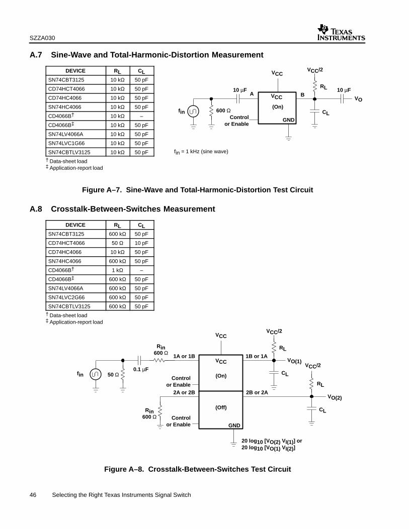
A.7 Sine-Wave and Total-Harmonic-Distortion Measurement
DEVICE RL CLSN74CBT3125 10 kΩ 50 pF
CD74HCT4066 10 kΩ 50 pF
CD74HC4066 10 kΩ 50 pF
SN74HC4066 10 kΩ 50 pF
CD4066B† 10 kΩ –
CD4066B‡ 10 kΩ 50 pF
SN74LV4066A 10 kΩ 50 pF
SN74LVC1G66 10 kΩ 50 pF
SN74CBTLV3125 10 kΩ 50 pF† Data-sheet load‡ Application-report load
Figure A–7. Sine-Wave and Total-Harmonic-Distortion Test Circuit
A.8 Crosstalk-Between-Switches Measurement
DEVICE RL CLSN74CBT3125 600 kΩ 50 pF
CD74HCT4066 50 Ω 10 pF
CD74HC4066 10 kΩ 50 pF
SN74HC4066 600 kΩ 50 pF
CD4066B† 1 kΩ –
CD4066B‡ 600 kΩ 50 pF
SN74LV4066A 600 kΩ 50 pF
SN74LVC2G66 600 kΩ 50 pF
SN74CBTLV3125 600 kΩ 50 pF† Data-sheet load‡ Application-report load
VO(1)1A or 1B 1B or 1A
2A or 2B 2B or 2A
GND
(On)
(Off)
VCC
VCC
RL
CL
VCC/2
VO(2)
RL
CL
VCC/2
50 Ω0.1 µF
Rin600 Ω
fin
Rin600 Ω Control
or Enable
Controlor Enable
20 log10 [VO(2) VI(1)] or20 log10 [VO(1) VI(2)]
Figure A–8. Crosstalk-Between-Switches Test Circuit

IMPORTANT NOTICE
Texas Instruments Incorporated and its subsidiaries (TI) reserve the right to make corrections, modifications,enhancements, improvements, and other changes to its products and services at any time and to discontinueany product or service without notice. Customers should obtain the latest relevant information before placingorders and should verify that such information is current and complete. All products are sold subject to TI’s termsand conditions of sale supplied at the time of order acknowledgment.
TI warrants performance of its hardware products to the specifications applicable at the time of sale inaccordance with TI’s standard warranty. Testing and other quality control techniques are used to the extent TIdeems necessary to support this warranty. Except where mandated by government requirements, testing of allparameters of each product is not necessarily performed.
TI assumes no liability for applications assistance or customer product design. Customers are responsible fortheir products and applications using TI components. To minimize the risks associated with customer productsand applications, customers should provide adequate design and operating safeguards.
TI does not warrant or represent that any license, either express or implied, is granted under any TI patent right,copyright, mask work right, or other TI intellectual property right relating to any combination, machine, or processin which TI products or services are used. Information published by TI regarding third–party products or servicesdoes not constitute a license from TI to use such products or services or a warranty or endorsement thereof.Use of such information may require a license from a third party under the patents or other intellectual propertyof the third party, or a license from TI under the patents or other intellectual property of TI.
Reproduction of information in TI data books or data sheets is permissible only if reproduction is withoutalteration and is accompanied by all associated warranties, conditions, limitations, and notices. Reproductionof this information with alteration is an unfair and deceptive business practice. TI is not responsible or liable forsuch altered documentation.
Resale of TI products or services with statements different from or beyond the parameters stated by TI for thatproduct or service voids all express and any implied warranties for the associated TI product or service andis an unfair and deceptive business practice. TI is not responsible or liable for any such statements.
Mailing Address:
Texas InstrumentsPost Office Box 655303Dallas, Texas 75265
Copyright 2001, Texas Instruments Incorporated


