
DAEWOO ELECTRONICS CO., LTD.http : //svc.dwe.co.kr
Service ManualXGA COLOR MONITOR
Model : 531X
September, 2000

CONTENTS
SAFETY PRECAUTIONS 1
GENERAL SAFETY INFORMATION 2
SERVICING PRECAUTIONS 3
TECHNICAL INFORMATION 6
GENERAL INFORMATION 7
PIN CONNECTOR 8
CAUTIONS FOR ADJUSTMENT AND REPAIR 8
OPERATION AND ADJUSTMENT 9
ALIGNMENT PROCEDURE 12
TROUBLESHOOTING HINTS 15
BLOCK DIAGRAM 29
PCB LAYOUT 30
SCHEMATIC DIAGRAM 33
EXPLODED VIEW DIAGRAM 37
INFORMATION OF PART DESCRIPTION 38
ELECTRICAL PARTS LIST 39
1
SAFETY PRECAUTIONS
Safety Check
Care should be taken while servicing this analog color display because of the high voltages used in the deflectioncircuits. These voltages are exposed in such areas as the associated flyback and yoke circuits.
Fire & Shock Hazard
• Insert an isolation transformer between the analog color display and AC power line before servicing thechassis.
• When servicing, pay close attention to the original lead dress especially in the high voltage circuit area;if a short circuit is found, replace all parts which have been overheated as a result of the short circuit.
• All the protective devices must be reinstalled per original design.• Soldering must be inspected for possible cold solder points, frayed leads, damaged insulation, solder
splashes or sharp solder points. Be certain to remove all foreign materials.
Implosion Protection
Picture tube in this monitor employs integral implosion protection system, but care should be taken toavoid damage and scratching during installation.Only use same type replacement picture tubes.
X-Ray
IMPORTANT SAFETY NOTICE: There are special components used in this analog color display,which are important for safety. These parts are shaded on theschematic diagram and on the replacement parts list. It is essentialthat these critical parts should be replaced with manufacturer’sspecified parts to prevent X-Ray, shock, fire or other hazards. Donot modify the original design without getting written permissionfrom DAEWOO ELECTRONICS CO. or this will void the originalparts and labor warranty.
CAUTION: No modifications of any circuits should be attempted. Service work should be performedonly after you are thoroughly familiar with all of the following safety checks and servicingguidelines.
WARNING: The only potential source of X-Ray is the picture tube. However when the high voltagecircuitry is operating properly, there is no possibility of an X-Ray problem. The basicprecaution which must be exercised is to keep the high voltage at the following factoryrecommended level.
NOTE: It is important to use an accurate, periodically, calibrated high voltage meter.• To measure the high voltage, use a high-impedance high-voltage meter.
Connect(-) to chassis and (+) to the CRT anode button.• Turn the Contrast & Brightness Control fully counterclockwise.• Measure the high voltage. The high voltage meter should indicate the following factory
recommended levels.• If the upper meter indication exceeds the maximum level, immediate service is required to
prevent the possibility of premature component failure.• To prevent X-Ray possibility, it is essential to use the specified picture tube.• The normal high voltage is 25.5KV or below and must not exceed 29KV at zero beam current
at rated voltage.
2
Warning: This product includes critical mechanical and electrical parts which are essential for x rayprotection. For continued safety, replace critical components that are indicated in the servicemanual with exact replacement parts given in the parts list.Operating high voltage with this product is 29Kv at minimum brightness. Refer to servicemanual for measurement procedures and proper service adjustments.
GENERAL SAFETY INFORMATION
Terms in the manual
CAUTION Statements identify conditions or practices that could result in damage to the equipment orother property.
WARNING Statements identify conditions or practices that could result in personal injury or loss oflife.
Terms as marked on equipment
CAUTION Statements indicate a personal injury hazard not immediately accessible as one reads themarking or a hazard which is properly included on the equipment itself.
WARNING Statements are clearly concerning indicated personal injury hazards.
Symbols in the manual
The symbols indicate where applicable cautionary or other information is to be found.
Symbols as marked on equipment
Protective GROUND terminal
High Voltage Warning And Critical Component Warning Label
The following warning label is on the CRT PWB shield case inside the unit.
3
SERVICING PRECAUTIONS
General Servicing Precautions
1. Always unplug the AC power cord from the AC power source before:a. Removing or reinstalling any component, circuit board, module, or any other instrument assembly.b. Disconnecting or reconnecting any electrical plug or other electrical connection.c. Connecting a test substitute in parallel with an electrolytic capacitor in the instrument.
d. Discharging the picture tube anode.
2. Test high voltage only by measuring it with an appropriate high voltage meter or other voltagemeasuring device (DVM, FETVOM. etc.) equipped with a suitable high voltage probe. Do not test highvoltage by “drawing an arc”.
3. Discharge the picture tube anode only by: (a) first connecting one end of an insulated clip lead to thedegaussing or line grounding system shield at the point where the picture tube socket ground lead isconnected, and then (b) touching the other end of the insulated clip lead to the picture tube anodebutton, using an insulating handle to avoid personal contact with high voltage.
4. Do not any spray chemicals on or near this instrument, or any of its assemblies.
5. Unless otherwise specified in this service manual, only clean electrical contacts by applying thefollowing mixture to the contacts with a pipe cleaner, cotton-tipped stick, or comparable nonabrasiveapplicator: 10% (by volume) Aceton and 90% (by volume) isopropyl alchohol (90%-99% strength).
6. Do not damage any plug/socket B+ voltage interlocks with which instruments covered by this servicemanual might be equipped.
7. Do not apply AC power to this instrument and/or any other of its electrical assemblies unless all thesolid-state device heat sinks are correctly installed.
8. Always connect the test instrument ground lead to the appropriate instrument chassis ground beforeconnecting the test instrument positive lead. Always remove the test instrument ground lead last.
9. Only use the test fixtures specified in this service manual with this instrument.
CAUTION: Before servicing instruments covered by this service manual, its supplements, andaddendum, please read and follow the SAFETY PRECAUTIONS of this manual.
NOTE: If unforeseen circumstances create conflict between the following servicing precautions and anyof the safety precautions on page 1 of this manual, always follow the safety precautions.Remember: Safety First.
CAUTION: A wrong part substitution or incorrect polarity installation of electrolytic capacitorsmay result in a explosion.
CAUTION: This is a flammable mixture. Unless specified in this service manual, lubrication of contacts isnot required.
CAUTION: Do not connect the test fixture ground strap to any heatsink in this instrument.
4
Electrostatically Sensitive (ES) Devices
Some semiconductor (solid state) devices can be damaged easily by static electricity.Such components are commonly called Electrostatically Sensitive (ES) Devices.The typical examples of ES devices are integrated circuits, some field-effect transistors, andsemiconductor “chip” components. The following techniques should be used to help reduce the incidenceof component damage caused by static electricity.
1. Immediately before handling any semiconductor component or semiconductor-equipped assembly,wipe off any electrostatic charge on your body by touching any known earth ground. Alternatively,obtain and wear a commercially available discharging wrist strap device which should be removed forpotential shock reasons prior to applying power to the unit under testing conditions.
2. After removing the electrical assembly equipped with ES devices, place the assembly on a conductivesurface such as aluminum foil to prevent electrostatic charge buildup or exposure to the assembly.
3. Only use a grounded-tip soldering iron to solder or unsolder ES devices.
4. Only use an anti-static type solder removal device. Some solder removal devices not classified as “anti-static” can generate enough electrical charges to damage ES devices.
5. Do not use freon-propelled chemicals. These can generate enough electrical charges to damage ES devices.
6. Do not remove a replacement ES device from its protective package until immediately before you areready to install it. (Most replacement ES devices are packaged with leads electrically shorted togetherby conductive foam, aluminum foil, or comparable conductive material).
7. Immediately before removing the protective material from the leads of replacement ES devices, touchthe protective material to the chassis or circuit assembly into which the device will be installed.
8. Minimize bodily movements when handling unpackaged replacement ES devices. (Otherwise harmfulmotion such as the brushing together clothes fabric or the lifting your foot from a carpeted floor cangenerate enough static electricity to damage ES devices).
General Soldering Guidelines
1. Use a grounded-tip, low-wattage soldering iron with appropriate tip size and shape that will maintaintip temperature between a 550°F-660°F (288°C-316°C) range.
2. Use an appropriate gauge of RMA resin-core solder composed of 60 parts tin/40 parts lead.
3. Keep the soldering iron tip clean.
4. Throughly clean the surface to be soldered. Use a small wire-bristle (0.5 inch or 1.25cm) brush with ametal handle. Do not use freon-propelled spray-on cleaners.
5. Use the following soldering technique:a. Allow the soldering iron tip to reach normal temperature (550°F to 660°F or 288°C to 316°C)b. Hold the soldering iron tip and solder strand against the component lead until the solder melts.c. Quickly move the soldering iron tip to the junction of the component lead and the printed circuit foil,
and hold it there until the solder flows onto and around both the component lead and the foil.d. Closely inspect the solder area and remove any excess or splashed solder with a small wire-bristle brush.
CAUTION: Be sure that no power is applied to the chassis or circuit, and observe all other safetyprecautions.
CAUTION: Work quickly to avoid overheating the circuit board printed foil.
5
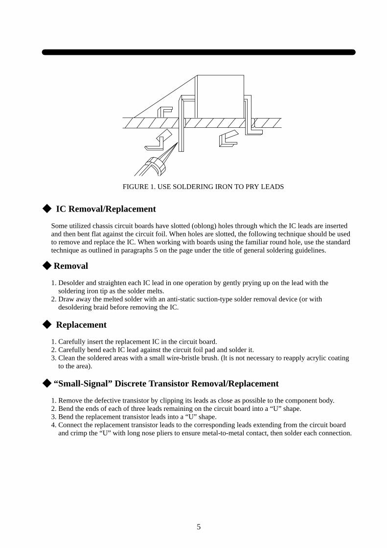
FIGURE 1. USE SOLDERING IRON TO PRY LEADS
IC Removal/Replacement
Some utilized chassis circuit boards have slotted (oblong) holes through which the IC leads are insertedand then bent flat against the circuit foil. When holes are slotted, the following technique should be usedto remove and replace the IC. When working with boards using the familiar round hole, use the standardtechnique as outlined in paragraphs 5 on the page under the title of general soldering guidelines.
Removal
1. Desolder and straighten each IC lead in one operation by gently prying up on the lead with thesoldering iron tip as the solder melts.
2. Draw away the melted solder with an anti-static suction-type solder removal device (or withdesoldering braid before removing the IC.
Replacement
1. Carefully insert the replacement IC in the circuit board.2. Carefully bend each IC lead against the circuit foil pad and solder it.3. Clean the soldered areas with a small wire-bristle brush. (lt is not necessary to reapply acrylic coating
to the area).
“Small-Signal” Discrete Transistor Removal/Replacement
1. Remove the defective transistor by clipping its leads as close as possible to the component body.2. Bend the ends of each of three leads remaining on the circuit board into a “U” shape.3. Bend the replacement transistor leads into a “U” shape.4. Connect the replacement transistor leads to the corresponding leads extending from the circuit board
and crimp the “U” with long nose pliers to ensure metal-to-metal contact, then solder each connection.
6
Power IC, Transistor or Devices Removal/Replacement
1. Heat and remove all solders from the device leads.2. Remove the heatsink mounting screw (if applicable).3. Carefully remove the device from the circuit board.4. Insert new device in circuit board.5. Solder each device lead and then clip off excess lead.6. Replace heatsink.
Diode Removal/Replacement
1. Remove defective diode by clipping its leads as close as possible to diode body.2. Bend the two remaining leads perpendicularly to the circuit board.3. Observing diode polarity, wrap each lead out of the new diode around the corresponding lead on the
circuit board.4. Securely crimp each connection and solder it.5. Inspect the solder joints of the two “original” leads on the circuit board copper side. If they are not
shiny, reheat them and apply additional solder if necessary.
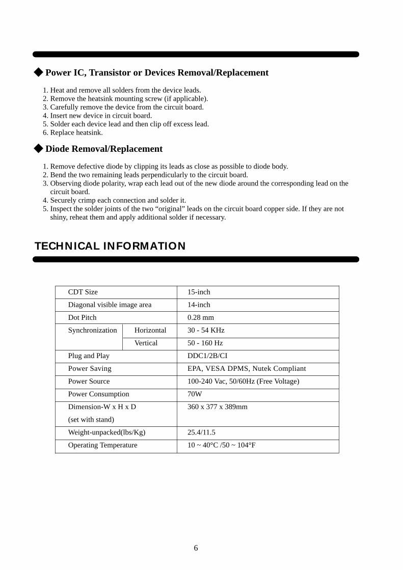
TECHNICAL INFORMATION
CDT Size 15-inch
Diagonal visible image area 14-inch
Dot Pitch 0.28 mm
Synchronization Horizontal 30 - 54 KHz
Vertical 50 - 160 Hz
Plug and Play DDC1/2B/CI
Power Saving EPA, VESA DPMS, Nutek Compliant
Power Source 100-240 Vac, 50/60Hz (Free Voltage)
Power Consumption 70W
Dimension-W x H x D 360 x 377 x 389mm
(set with stand)
Weight-unpacked(lbs/Kg) 25.4/11.5
Operating Temperature 10 ~ 40°C /50 ~ 104°F
This color monitor automatically scans all horizontal frequencies from 30KHz to 54KHz, and all vertical frequencies from50Hz to 160Hz. This color monitor supports IBM PC, PC/XT, PC/AT, personal System/2 (PS/2), Apple Macintosh, andcompatible users crisp text and vivid color graphics display when using the following graphics adapters : (VGA, 8514/A,Super VGA, VESA and XGA and Apple Macintosh Video Card). And so, this color monitor has a maximum horizontalresolution of 1024 dots and a maximum vertical resolution of 768 lines for superior clarity of display.By accepting analog signal inputs which level is zero to 0.7 Volts. This color monitor can display and unlimited palette ofcolors depending on the graphics adapter and software being used.
Abbreviations
7
GENERAL INFORMATION
ADJ Adjustment
AFC Automatic Frequency Control
CRT Cathode Ray Tube
Def Deflection
D.Y Deflection Yoke
FBT Flyback Transformer
H.SYNC Horizontal Synchronization
OSC Oscillator
P.S.U Power Supply Unit
PWA Printed Circuit Board Wiring Assembly
R.G.B Red, Green, Blue
V.Sync Vertical Synchronization
8
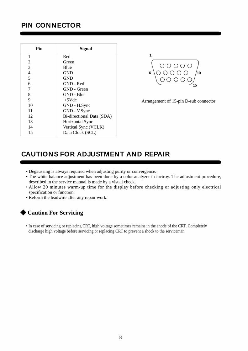
Pin Signal
1 Red2 Green3 Blue4 GND5 GND6 GND - Red7 GND - Green8 GND - Blue9 +5Vdc10 GND - H.Sync11 GND - V.Sync12 Bi-directional Data (SDA)13 Horizontal Sync14 Vertical Sync (VCLK)15 Data Clock (SCL)
• Degaussing is always required when adjusting purity or convergence.• The white balance adjustment has been done by a color analyzer in factroy. The adjustment procedure,
described in the service manual is made by a visual check.• Allow 20 minutes warm-up time for the display before checking or adjusting only electrical
specification or function.• Reform the leadwire after any repair work.
Caution For Servicing
• In case of servicing or replacing CRT, high voltage sometimes remains in the anode of the CRT. Completelydischarge high voltage before servicing or replacing CRT to prevent a shock to the serviceman.
Arrangement of 15-pin D-sub connector
PIN CONNECTOR
CAUTIONS FOR ADJUSTMENT AND REPAIR
1
6
15
10
9
OPERATION AND ADJUSTMENT
Control Panel
• Move cursor to the right window on the OSD window.
• Increase the value of any selected function.
• Move cursor to the left window on the OSD window.
• Decrease the value of any selected function.
• Launch OSD(On-Screen Display) MENU window.
• Move cursor to the high window on the OSD window.
• Increase the value of V.size or V.center.
• Move cursor to the low window on the OSD window.
• Decrease the value of V.size or V.center.
10
• When you choose the icon on the OSD window, you can exit the OSD screen.
OSD OFF
MENU
MENU
MENU
MENU
Key Process
11
OSD Functions
ICON CONTROL FUNCTIONS
Adjust the pin corner bottom when the bottom sides of the screen are bowed.B. PIN CORNER
Adjust the parallelogram when the screen is leaning left or right.
Adjust the pin corner top when the top sides of the screen are bowed.T. PIN CORNER
PARALLELOGRAM
Adjust the trapezoid of the screen by moving the lines inward or outward.
Adjust the side balance when the sides of the screen are bowed towards left or right.PIN BALANCE
TRAPEZOID
Adjust the left and right margins for more convex or more concave margins.PINCUSHION
Choose different preset color temperatures or set your own customized color parameters.COLOR TEMP
Adjust the position of the display horizontally (left or right) and vertically (up or down).H. CENTER &
V. CENTER
Adjust the red gain.
Adjust the green gain.
Adjust the blue gain.
RED GAIN
GREEN GAIN
BLUE GAIN
Adjust the width (horizontal size) and the height (vertical size) of the display.H. SIZE &
V. SIZE
Display horizontal & vertical frequency and polarity.STATUS
Degaussing keeps the monitor free from unwanted magnetism that can result in colorimpurity.DEGAUSS
12
Reset the screen to the Factory Preset Display Settings.RECALL
ICON CONTROL FUNCTIONS
Adjust the vertical picture moire cancellation.V. MOIRE
Adjust the horizontal picture moire cancellation.H. MOIRE
Select language for OSD (5 languages).LANGUAGE
ALIGNMENT PROCEDURE
Standard Adjustment Conditions1. Power source voltage : 100-240Vac 50/60Hz2. Aging : Take at least 20 minutes warm-up time.3. Signals
Video : Analog 0.7Vpp 75Ω terminal positive polaritySynchronizing : TTL level Negative/Positive SeparateDeflection frequency
Horizontal Frequency : 30KHz - 54KHzVertical Frequency : 50Hz - 160Hz
Pre-Adjustment1. B+ Adjustment
Adjust 50Vdc ± 0.1Vdc between D102 cathode and ground at 31.5KHz mode, varying VR001.Adjust 59Vdc ± 0.1Vdc between D510 cathode and ground at 31.5KHz mode, varying VR501.
Method to launch the factory modeStep 1. Push the menu button.
Step 2. Push the menu button and plus control button ( ) for 5 times in same time.
Main Adjustment1. Setting the Controls
Set the value of items as following.Contrast : Max.(OSD value up to MAX)Brightness : Center(Set the OSD value to center)
2. H.size, V.size, H.center, V.center, Pin Balance, Pincushion, TrapezoidReceive the cross hatch pattern of Factory preset mode.H.size, V.size, H.center, V.center, Pin Balance, Pincushion, Trapezoid are adjusted at each mode.In Factory, Auto Alignment was done at each mode. Therefore, Factory preset mode has it’sown value according to each control.
3. Focus(a) Set brightness control to center and contrast control to MAX.(b) Receive all “H” character pattern of 1024 X 768 (48KHz, 60Hz)(c) Adjust the Focus control of FBT to obtain best Focus.
4. Geometric Distortion Adjustment.(a) Receive the cross hatch pattern of factory preset mode.(b) Pincushion, Trapezoid, Pin Balance are adjusted the best geometric status.
5. White Balance Adjustment(a) Select 9300°K on the OSD Menu.(b) Receive a full white pattern of 54KHz mode signal by using the signal generator.(c) Set the brightness control to the maximum, the contrast control to the maximum.(d) Cut off the FBT screen VR.(e) Receive all the black patterns. The luminance of the screen should be 0.5~1.0 Ft-L by using Screen
VR.(f) Select the R-BIAS, G-BIAS and B-BIAS on the control menu and adjust the +/– key to get the color
coordinates in x=0.281 ± 0.015, y=0.311± 0.015.(g) Receive a full white pattern. Adjust the brightness value to the center.(h) Select the R-GAIN and B-GAIN and adjust the +/– key to get the color coordinates in x=0.281 ±
0.015, y=0.311 ± 0.015.(i) Adjust the ABL control to get the screen luminance to 30 Ft/L (a full white pattern over 30 Ft/L) (j) Check if the x, y coordinates of color analyzer is in x=0.281±0.015, y=0.311±0.015.
If the color coordinates is out of range, adjust the R. G. B BIAS & GAIN to get the coorinates inx=0.281, y=0.311. Make sure that the coordinates is in range.
(k) Select 6550°K on the OSD Menu and set the color coordinates in x=0.313, y=0.329 at themaximum contrast control and center brightness control
(l) Check if a full white pattern is over 30Ft/L.
13
14
6. Static Convergence Adjustment(a) Apply a magenta cross hatch pattern on display.(b) Adjust the focus from the best over all focus on the display.
Also adjust the brightness to the desired condition.(c) Vertical red and blue lines are converged by varying the angle between the two tabs of the 4-pole
magnets.(d) Horizontal red and blue lines are converged by varying the tabs together, keeping the angle between
them constant.(e) Apply a yellow cross hatch pattern on display.(f) Vertical green and red lines are converged by barying the angle between the two tabs of the 6-pole
magnets.(g) Horizontal green and red lines are converged by varying the tabs together, keeping the angle
between them constant.
15
TROUBLESHOOTING HINTS
1. No Character
Change the Contrast &Brightness control value tomaximum
No Raster Refer toNo Raster
Check the peripheral circuitof CRT
Check the video outputcircuit and its ambient circuit
Trouble in 12V lineof the Main PWB
Check the clamping pulse circuit
Check the signal cable
No Character
Is wholescreen bright?
Yes
Yes
Yes
Yes
Yes
No
No
No
No
No
Yes
Yes
Rk, Gk, Bk
About 30~35Vpp
No
No
Is CRTCathode (Rk, Gk, Bk)
signal levelnormal?
Is theoutput signal of the
(pin 14, 16, 18) pre-ampIC801, normal?
Is blanking pulse (pin 20 of IC801)
normal?
Is 12V linenormal?
Is input signalnormal?
Trouble in IC801 andits ambient circuit
5Vp-p
Are the Contrast &Brightness Controls in
OSD menu maximum?
16
2. No Raster
Trouble inpower supplycircuit
Trouble in powersupply circuit
Trouble in G1line
Trouble in FBT or itspin4 ambient circuit
High Voltagetrouble in FBT
Trouble in 100Vdc line of power supply unit
Refer to troublein P.S.U
Refer to trouble inpower supply unit.
Is CRTheater red-hot?
No
Yes
No
No
No
No
Yes
No
Yes
Yes
Yes
Yes
No
Is HeaterVoltage (CRT PWB)
about 6V?
Turn the Brightness& Contrast control to set Maximum
No Raster
Is wholescreen bright?
CheckG1 voltage about
-60V?
Is 100Vdcline normal?
Doesthe Brightness control
make screenbright?
Is CRTG2 (screen) voltage
about 730V?
Trouble inCRT
Raster OK
Yes
Yes
17
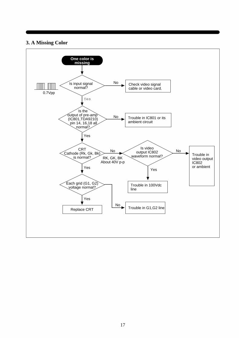
3. A Missing Color
Is input signalnormal?
One color ismissing
CRTCathode (Rk, Gk, Bk)
is normal?
Is videooutput IC802
waveform normal?
Each grid (G1, G2)voltage normal?
Is theoutput of pre-amp (IC801,TDA9210) pin 14, 16,18 all
normal?
Check video signalcable or video card.
Trouble in IC801 or itsambient circuit
Trouble invideo outputIC802or ambient
Trouble in 100Vdcline
Trouble in G1,G2 lineReplace CRT
No
No
No No
No
Yes
Yes Yes
Yes
Yes
RK, GK, BKAbout 40V p-p
0.7Vpp
18
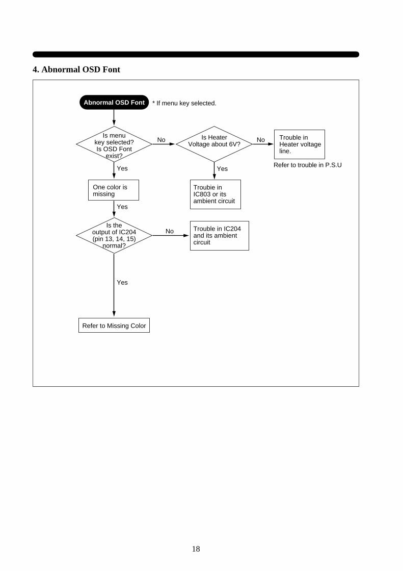
4. Abnormal OSD Font
Is menukey selected?Is OSD Font
exist?
* If menu key selected.
Is HeaterVoltage about 6V?
Abnormal OSD Font
Is theoutput of IC204(pin 13, 14, 15)
normal?
Trouble inHeater voltage line.
Refer to trouble in P.S.U
Troubie inIC803 or itsambient circuit
Trouble in IC204and its ambientcircuit
One color ismissing
Refer to Missing Color
No
No
YesYes
Yes
Yes
No
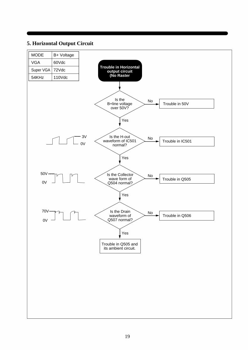
MODE B+ Voltage
VGA 60Vdc
Super VGA 72Vdc
54KHz 110Vdc
19
5. Horizontal Output Circuit
Is theB+line voltage
over 50V?
Is the H-outwaveform of IC501
normal?Trouble in IC501
Trouble in Horizontaloutput circuit
(No Raster
Yes
No
Is the Collectorwave form of
Q504 normal?
Yes
Yes
Yes
Trouble in Q505No
No
No
Trouble in Q505 andits ambient circuit.
3V
0V
50V
Is the Drainwaveform of
Q507 normal?
Trouble in 50V
Trouble in Q506
0V
0V
70V
20
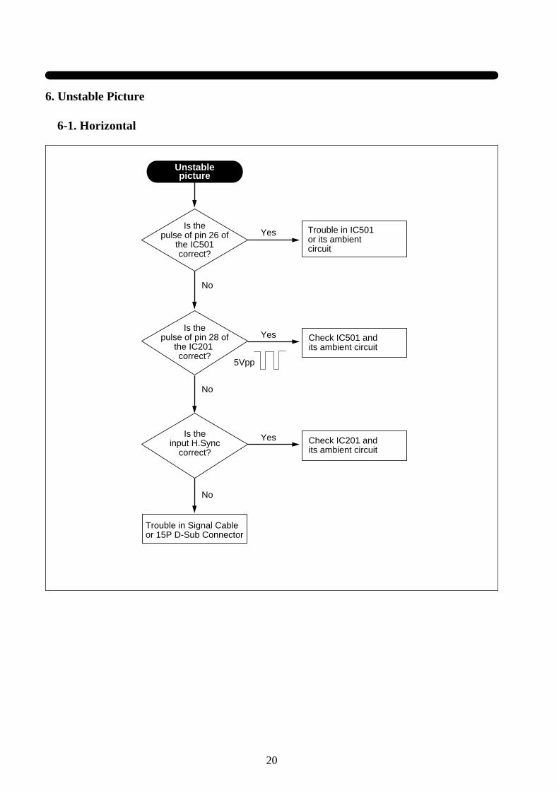
6. Unstable Picture
6-1. Horizontal
Unstablepicture
Is thepulse of pin 26 of
the IC501correct?
Trouble in IC501or its ambientcircuit
Is thepulse of pin 28 of
the IC201 correct?
Check IC501 andits ambient circuit
No
No
No
Yes
Yes
Is theinput H.Sync
correct?Check IC201 andits ambient circuit
Yes
Trouble in Signal Cableor 15P D-Sub Connector
5Vpp
21
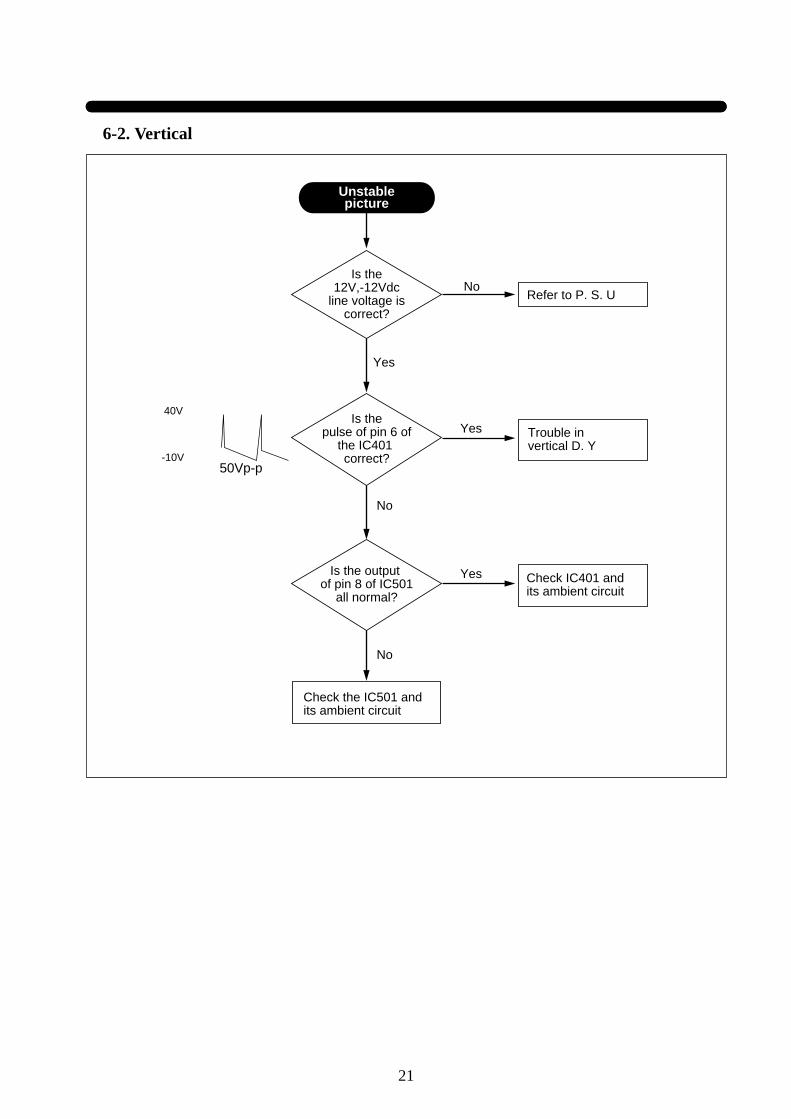
6-2. Vertical
Unstablepicture
Is the12V,-12Vdc
line voltage iscorrect?
Refer to P. S. U
Is thepulse of pin 6 of
the IC401 correct?
Trouble in vertical D. Y
No
No
No
Yes
Yes
Is the output of pin 8 of IC501
all normal?
Check IC401 andits ambient circuit
Yes
Check the IC501 and its ambient circuit
50Vp-p
40V
-10V
22
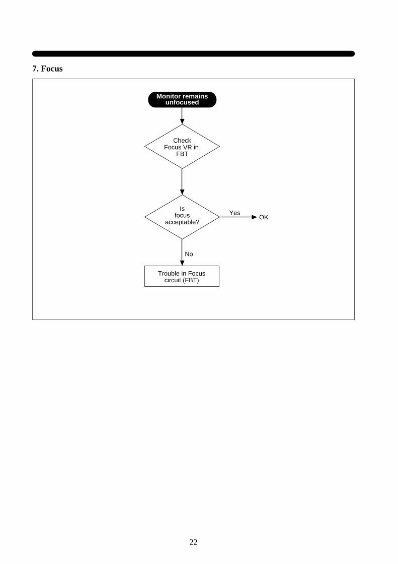
7. Focus
Monitor remainsunfocused
CheckFocus VR in
FBT
Isfocus
acceptable?
Trouble in Focuscircuit (FBT)
YesOK
No

23
8. Convergence
Isconvergence
on the center areabad?
Isconvergence on the
fringe area bad?
Adjust staticconvergence
Refer toAdjustmentprocedure ofconvergence
Yes
Adjust D.YLocation
Yes
No
Poor convergence
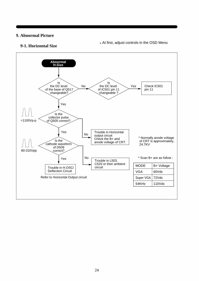
MODE B+ Voltage
VGA 60Vdc
Super VGA 72Vdc
54KHz 110Vdc
24
9. Abnormal Picture
9-1. Horizontal Size
Trouble in L503,C520 or their ambientcircuit
Trouble in Horizontaloutput circuitCheck the B+ andanode voltage of CRT.
Trouble in H.OSC/Deflection Circuit
Refer to Horizontal Output circuit
Isthe DC level
of the base of Q517 changeable?
No
Yes
Isthe DC level
of IC501 pin 11changeable ?
Yes Check IC501 pin 11
Is thecollector pulse
of Q505 correct?
Is thecathode waveform
of D509correct?
AbnormalH.Size
=1100Vp-p
80-310Vpp
* Normally anode voltage of CRT is approximately, 24.7KV
* Scan B+ are as follow :
NoYes
Yes No
* At first, adjust controls in the OSD Menu
25
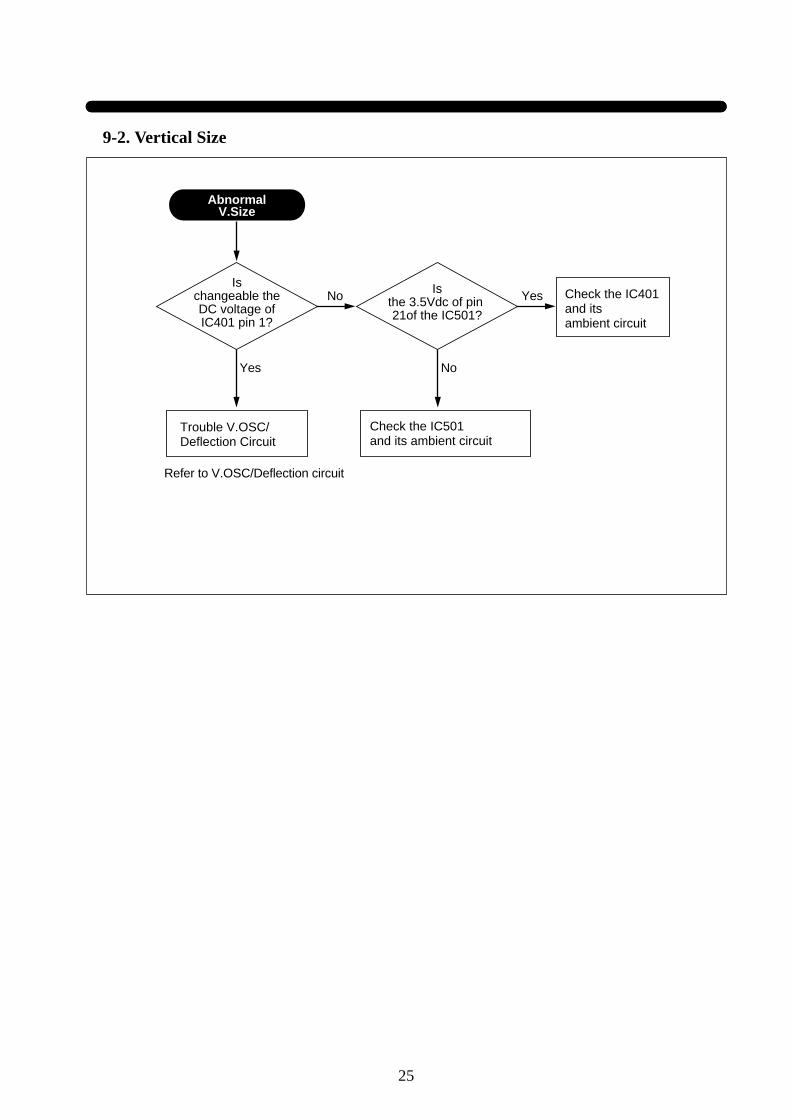
9-2. Vertical Size
Ischangeable theDC voltage ofIC401 pin 1?
Check the IC401and itsambient circuit
Check the IC501 and its ambient circuit
No
No
Trouble V.OSC/Deflection Circuit
Refer to V.OSC/Deflection circuit
Yes
Isthe 3.5Vdc of pin 21of the IC501?
Yes
AbnormalV.Size
26
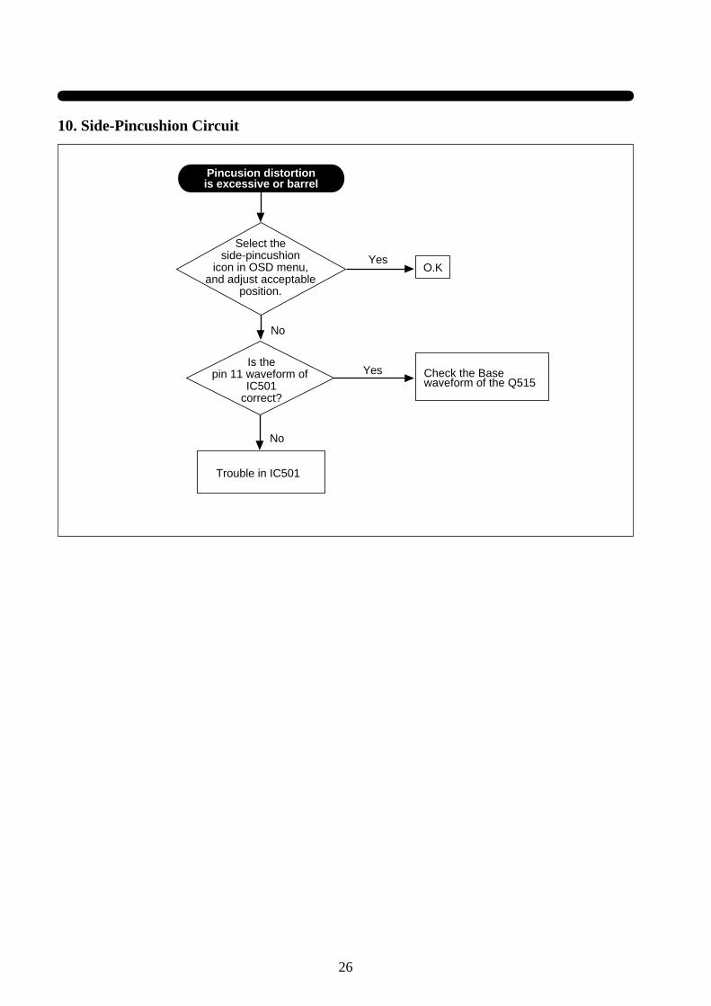
10. Side-Pincushion Circuit
Check the Base waveform of the Q515
Yes
Pincusion distortionis excessive or barrel
O.K
Select theside-pincushion
icon in OSD menu,and adjust acceptable
position.
Yes
Is thepin 11 waveform of
IC501correct?
No
No
Trouble in IC501
27
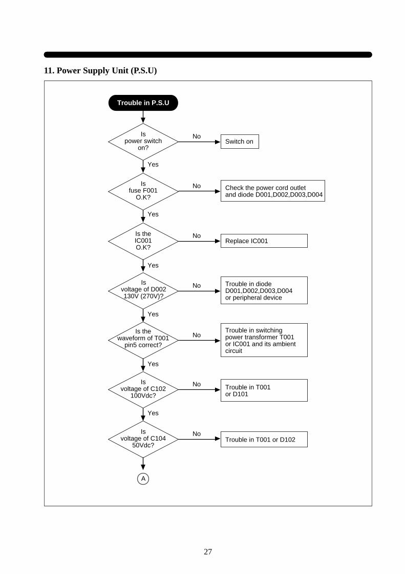
11. Power Supply Unit (P.S.U)
Is theIC001O.K?
Replace IC001No
Isvoltage of C104
50Vdc?
No
Isvoltage of D002130V (270V)?
Trouble in switchingpower transformer T001or IC001 and its ambientcircuit
Trouble in diodeD001,D002,D003,D004or peripheral device
No
Is thewaveform of T001
pin5 correct?
Trouble in T001or D101
No
Trouble in P.S.U
Ispower switch
on?Switch on
No
Yes
Yes
Yes
Yes
Yes
Yes
Isvoltage of C102
100Vdc?
Trouble in T001 or D102
No
Isfuse F001
O.K?
Check the power cord outletand diode D001,D002,D003,D004
No
A

28
Is voltageof C1058Vdc?
Trouble in D103No
Is voltageof C109 13Vdc?
No
Yes
Yes
Yes
Is voltage of C108
-12Vdc?Trouble in D104 or vertical part
P.S.U O.K
Trouble in D106 or horizontal part
No
A
29
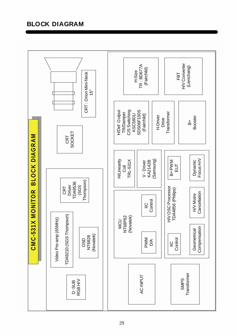
BLOCK DIAGRAMC
MC
-531
X M
ON
ITO
R B
LOC
K D
IAG
RA
M
CR
TS
OC
KE
T
CR
T :
Orio
n M
ini-N
eck
15"
D -S
UB
RG
B H
/V
Vid
eo P
re-a
mp
(65M
Hz)
TD
A92
10 (
SG
S T
hom
pson
)
OS
DN
T68
28(N
ovat
ek)
CR
TD
river
TD
A95
36(S
GS
Tho
mps
on)
AC
INP
UT
SM
PS
Tra
nsfo
rmer
MC
UN
T68
P62
(Nov
atek
)
H/V
OS
C P
roce
ssor
TD
A48
56 (
Phi
lips)
V -
Driv
erK
A21
42B
(Sam
sun g
)
PW
MD
/AIIC
Con
trol
H/L
inea
rity
Coi
lT
RL-
531X
H/D
ef O
utpu
tT
R/D
ampe
rC
/S S
witc
hin g
KS
C58
01/
SD
S06
F150
S(F
airc
hild
)
IICC
ontr
olB
+ P
WM
EU
T
Geo
met
rical
Com
pens
atio
nH
/V M
oire
Can
cella
tion
Dyn
amic
Foc
us H
/V
H-D
river
Driv
eT
rans
form
er
B+
Boo
ster
H-S
ize
TR
: B
D67
7A(F
airc
hild
)
FB
TH
/V C
onv
erte
r(L
ienc
han g
)
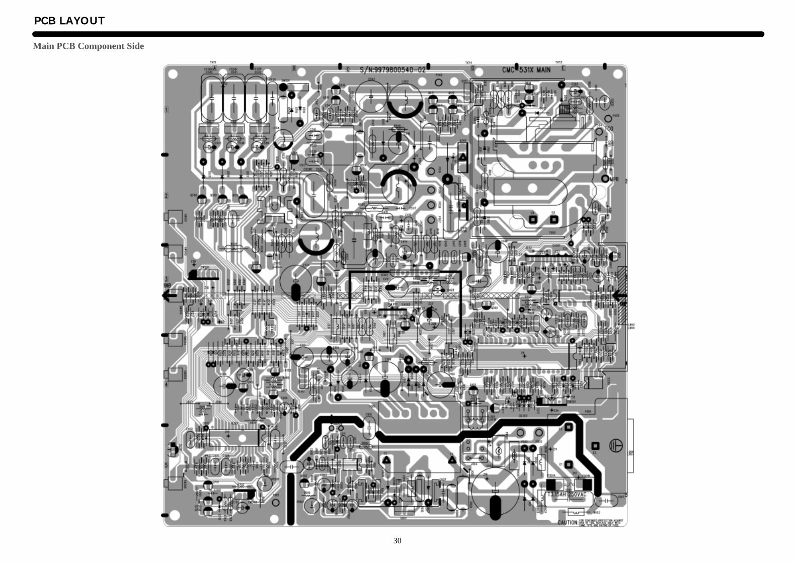
PCB LAYOUT
30
Main PCB Component Side
31
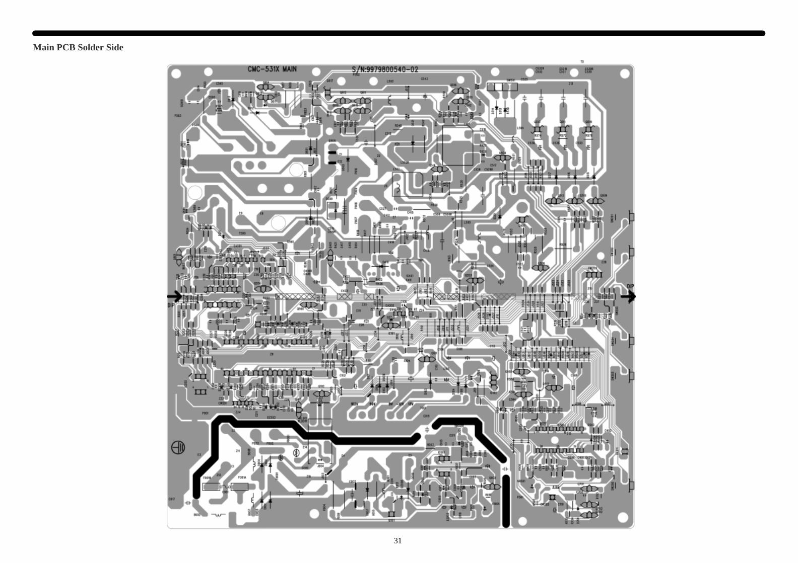
Main PCB Solder Side
32
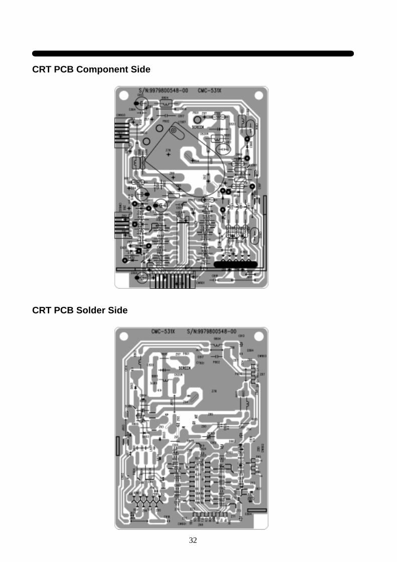
CRT PCB Component Side
CRT PCB Solder Side
33
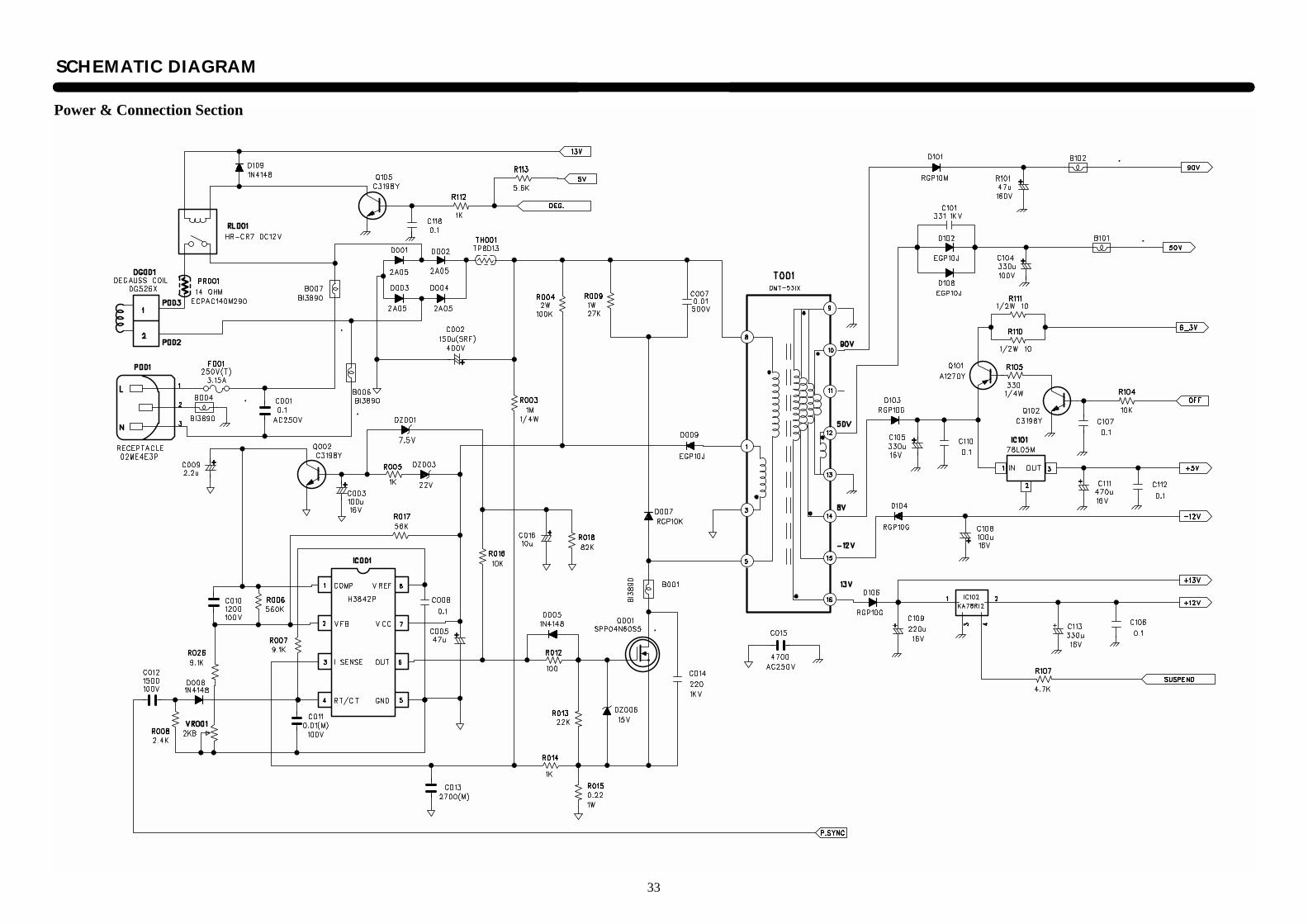
SCHEMATIC DIAGRAM
Power & Connection Section
34
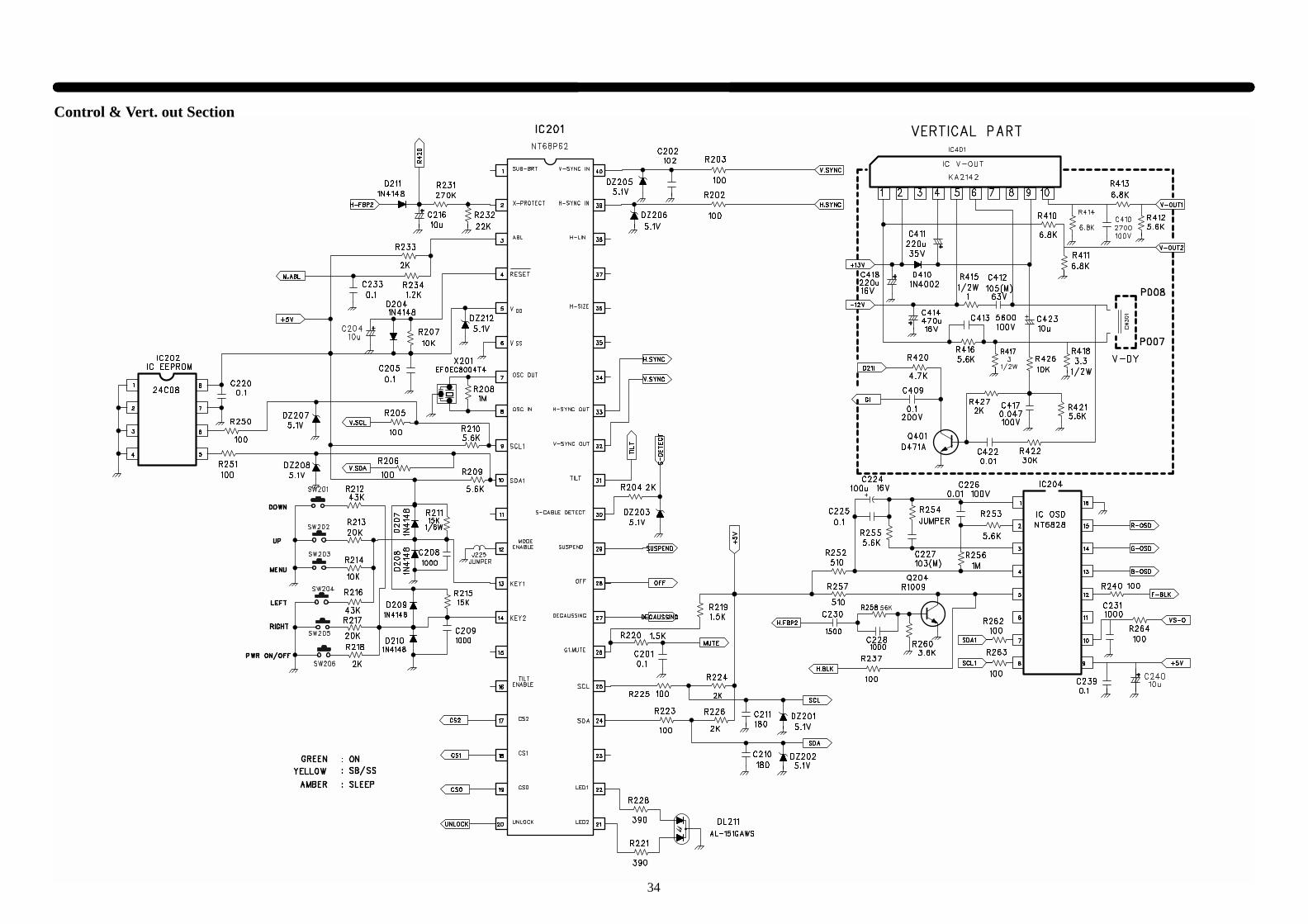
Control & Vert. out Section
35
Horizontal Section
36
Video Section
EXPLODED VIEW DIAGRAM
37
38
RESISTOR Description
Example:
CAPACITOR Description
Example:
Fig & Part No DescriptionIndex
CapacitorsC102 CCXF1H104Z Ceramic 50V 0.1µF ZC402 CCXB1H331K Ceramic 50V 330PF KC105 CMXM 2A224J MYLAR 100V 0.22µFJ
AllowanceC ± 0.25pFD ± 0.5%F ± 1pFJ ± 5%K ± 10%P ± 100% ~ 0%Z ± 80% ~ –
Fig & Part No DescriptionIndex
R101Resistors
RD-4Z820J Carbon: 82JR102 RD-4Z201J Carbon1/4W-200J
AllowanceF ± 1%J ± 5%K ± 10%M ± 20%G ± 2%
INFORMATION OF PART DESCRIPTION
Important Safety Notice
Components identified with the International Symbol have special characteristics important for safety.When replacing any components, use only manufacturer’s specified parts.
Abbreviation of Description

39
00001 9979800540 PCB MAIN T=1.6*246*247 (531X)
00002 9979800548 PCB CRT T=1.6*108*82(531X)
00020 W3475N731- CORD POWER 3 H05VV-F 3X0.75 1.8 IV
B001 5PB13890-- COIL BEAD BI3890
B006 5PB13890-- COIL BEAD BI3890
B007 5PB13890-- COIL BEAD BI3890
B101 5PB13857-- COIL BEAD BI3857(AXIAL)
B102 5PB13857-- COIL BEAD BI3857(AXIAL)
B501 5PB13857-- COIL BEAD BI3857(AXIAL)
B503 5PB13857-- COIL BEAD BI3857(AXIAL)
B801 5PB13857-- COIL BEAD BI3857(AXIAL)
B802 5PB13857-- COIL BEAD BI3857(AXIAL)
B803 5PB13857-- COIL BEAD BI3857(AXIAL)
B804 5PB13857-- COIL BEAD BI3857(AXIAL)
C001 CL1UC3104M C LINE ACROSS WORLD AC250V 0.1UF M R.47
C002 CEYP2G151Z C ELECTRO 400V SMH 150MF (25.4*40)
C003 CEXF1C101V C ELECTRO 16V RSS 100MF (6.3X11) TP
C005 CEXF1H470V C ELECTRO 50V RSS 47MF (6.3X11) TP
C007 CCXB2H103K C CERA HIKB 500V 0.01MF K
C008 CCXF1H104Z C CERA 50V F 0.1MF Z
C009 CEXF1H229V C ELECTRO 50V RSS 2.2MF (5X11) TP
C010 CMXM2A102J C MYLAR 100V 1000PF J (TP)
C011 CMXM2A103J C MYLAR 100V 0.01MF J (TP)
C012 CMXM2A152J C MYLAR 100V 1500PF J (TP)
C013 CMXM2A272J C MYLAR 100V 2700PF J (TP)
C014 CCXB3A221K C CERA 1KV B 220PF K (TAPPING)
C015 CH1FDF472M C CERA AC 2.5KV 4700PF M AC250V
C016 CEXF1H100V C ELECTRO 50V RSS 10MF (5X11) TP
C101 CCXB3A331K C CERA 1KV B 330PF K (TAPPING)
C102 CEXF2C470V C ELECTRO 160V RSS 47MF (13X25) TP
C104 CEXF2A331V C ELECTRO 100V RSS 330MF (16X25) TP
C105 CEXF1C331V C ELECTRO 16V RSS 330MF (8X11.5) TP
C106 CCXF1H104Z C CERA 50V F 0.1MF Z
C107 CCXF1H104Z C CERA 50V F 0.1MF Z
C108 CEXF1C101V C ELECTRO 16V RSS 100MF (6.3X11) TP
C109 CEXF1C221V C ELECTRO 16V RSS 220MF (8X11.5) TP
C110 CCXF1H104Z C CERA 50V F 0.1MF Z
C111 CEXF1C471V C ELECTRO 16V RSS 470MF (10X12.5)TP
C112 CCXF1H104Z C CERA 50V F 0.1MF Z
C113 CEXF1C331V C ELECTRO 16V RSS 330MF (8X11.5) TP
C118 CCXF1H104Z C CERA 50V F 0.1MF Z
C201 CCXF1H104Z C CERA 50V F 0.1MF Z
C202 CCXB1H102K C CERA 50V B 1000PF K (TAPPING)
C204 CEXF1H100V C ELECTRO 50V RSS 10MF (5X11) TP
C205 CCXF1H104Z C CERA 50V F 0.1MF Z
C208 CCXB1H102K C CERA 50V B 1000PF K (TAPPING)
C209 CCXB1H102K C CERA 50V B 1000PF K (TAPPING)
ELECTRICAL PARTS LIST
The components identified by mark have special characteristics important for safety and x-rayradiation. These should be replaced only with the types specified in the parts list.
LOC PART-CODE PART-NAME PART-DESC
C210 CCXB1H181K C CERA 50V B 180PF K (TAPPING)
C211 CCXB1H181K C CERA 50V B 180PF K (TAPPING)
C216 CEXF1H100V C ELECTRO 50V RSS 10MF (5X11) TP
C220 CCXF1H104Z C CERA 50V F 0.1MF Z
C224 CEXF1C101V C ELECTRO 16V RSS 100MF (6.3X11) TP
C225 CCXF1H104Z C CERA 50V F 0.1MF Z
C226 CMXM2A103J C MYLAR 100V 0.01MF J (TP)
C227 CMXM2A103J C MYLAR 100V 0.01MF J (TP)
C228 CCXB1H102K C CERA 50V B 1000PF K (TAPPING)
C230 CCXB1H152K C CERA 50V B 1500PF K (TAPPING)
C231 CCXB1H102K C CERA 50V B 1000PF K (TAPPING)
C233 CCXF1H104Z C CERA 50V F 0.1MF Z
C239 CCXF1H104Z C CERA 50V F 0.1MF Z
C240 CEXF1H100V C ELECTRO 50V RSS 10MF (5X11) TP
C401 CMXM2A104J C MYLAR 100V 0.1MF J (TP)
C402 CMXM2A154J C MYLAR 100V 0.15MF J (TP)
C409 CMXM2E104J C MYLAR 250V 0.1MF J
C410 CMXM2A272J C MYLAR 100V 2700PF J (TP)
C411 CEXF1V221V C ELECTRO 35V RSS 220MF (10X12.5)TP
C412 CMXL1J105J C MYLAR MEU 63V 1MF J
C413 CMXM2A562J C MYLAR 100V 5600PF J (TP)
C414 CEXF1C471V C ELECTRO 16V RSS 470MF (10X12.5)TP
C417 CMXM2A473J C MYLAR 100V 0.047MF J (TP)
C418 CEXF1C221V C ELECTRO 16V RSS 220MF (8X11.5) TP
C422 CCXB1H103K C CERA 50V B 0.01MF K
C423 CEXF1H100V C ELECTRO 50V RSS 10MF (5X11) TP
C504 CMXM2A223J C MYLAR 100V 0.022MF J TP
C505 CMXM2A332J C MYLAR 100V 3300PF J (TP)
C506 CEXF1C331V C ELECTRO 16V RSS 330MF (8X11.5) TP
C507 CMXM2A562J C MYLAR 100V 5600PF J (TP)
C508 CMXM2A103J C MYLAR 100V 0.01MF J (TP)
C509 CMXM2A104J C MYLAR 100V 0.1MF J (TP)
C510 CMXM2A822J C MYLAR 100V 8200PF J (TP)
C512 CCXF1H104Z C CERA 50V F 0.1MF Z
C514 CEXF1C220V C ELECTRO RSS 16V 22MF 5*11
C515 CMXM2A104J C MYLAR 100V 0.1MF J (TP)
C516 CMXM2A104J C MYLAR 100V 0.1MF J (TP)
C517 CMXM2A104J C MYLAR 100V 0.1MF J (TP)
C519 CMYH3C472J C MYLAR 1.6KV BUP 4700PF J
C520 CMXE2J562J C MYLAR 630V PU 5600PF J (TP)
C521 CCXB1H271K C CERA 50V B 270PF K (TAPPING)
C522 CCXB2H331K C CERA 500V B 330PF K (TAPPING)
C524 CEXF2A331V C ELECTRO 100V RSS 330MF (16X25) TP
C527 CCXB3A102K C CERA 1KV B 1000PF K (TAPPING)
C528 CMYF2D564J C MYLAR 200V MPP 0.56MF J
C531 CMXF2D224J C MYLAR MPP 200V 0.22MF J
C532 CMYF2D684J C MYLAR 200V MPP 0.68MF J
LOC PART-CODE PART-NAME PART-DESC
!
!
!
40
C536 CEXF1H109V C ELECTRO 50V RSS 1MF (5X11) TP
C538 CEXF1H109V C ELECTRO 50V RSS 1MF (5X11) TP
C541 CMXM2A103J C MYLAR 100V 0.01MF J (TP)
C542 CMXM2A152J C MYLAR 100V 1500PF J (TP)
C543 CEXD1H339W C ELECTRO 50V RHD 3.3MF(16*25)
C550 CMXM2A224J C MYLAR 100V 0.22MF J
C551 CMXM2A222J C MYLAR 100V 2200PF J (TP)
C552 CMXM2A223J C MYLAR 100V 0.022MF J TP
C556 CMYF2D105J C MYLAR MPP 200V 1MF J
C560 CEXF2C100V C ELECTRO 160V RSS 10MF (10X16) TP
C580 CMXM2A393J C MYLAR 100V 0.039MF J (TP)
C593 CMXM2A103J C MYLAR 100V 0.01MF J (TP)
C594 CEXF1H339V C ELECTRO 50V RSS 3.3MF (5X11) TP
C595 CEXF1H100V C ELECTRO 50V RSS 10MF (5X11) TP
C601 CCXB3A103K C CERA HIKB 1KV 0.01MF K
C611 CCXF1H104Z C CERA 50V F 0.1MF Z
C612 CCXB2H101K C CERA 500V B 100PF K (TAPPING)
C613 CCXB3A102K C CERA 1KV B 1000PF K (TAPPING)
C614 CXSL3A470K C CERA 1KV SL 47PF K (TP)
C615 CCXB2H271K C CERA 500V B 270PF K (TAPPING)
C801 CCXF1H104Z C CERA 50V F 0.1MF Z
C802 CMXL2E104J C MYLAR MEU 250V 0.1MF J
C803 CCXB1H682K C CERA 50V B 6800PF K (TAPPING)
C804 CEXF1H339V C ELECTRO 50V RSS 3.3MF (5X11) TP
C811 CEXF1C101V C ELECTRO 16V RSS 100MF (6.3X11) TP
C812 CEXF1E470V C ELECTRO 25V RSS 47MF (5X11) TP
C813 CEXF1E101V C ELECTRO 25V RSS 100MF (6.3X11) TP
C814 CMXL2E104J C MYLAR MEU 250V 0.1MF J
C815 CCXF1H104Z C CERA 50V F 0.1MF Z
C816 CCXF1H104Z C CERA 50V F 0.1MF Z
C817 CCXB2H103K C CERA HIKB 500V 0.01MF K
C818 CCXF1H104Z C CERA 50V F 0.1MF Z
C820 CCYB3A103K C CERA 1KV B 0.01MF K
C821 CCXB1H101K C CERA 50V B 100PF K (TAPPING)
C822 CCXB1H101K C CERA 50V B 100PF K (TAPPING)
C823 CCXB1H101K C CERA 50V B 100PF K (TAPPING)
C824 CCXB1H101K C CERA 50V B 100PF K (TAPPING)
C825 CCXB2H471K C CERA 500V B 470PF K (TAPPING)
C826 CCXF1H104Z C CERA 50V F 0.1MF Z
C827 CCXF1H104Z C CERA 50V F 0.1MF Z
C831 CCXF1H104Z C CERA 50V F 0.1MF Z
C833 CCXB1H682K C CERA 50V B 6800PF K (TAPPING)
C861 CCXF1H104Z C CERA 50V F 0.1MF Z
C862 CCXF1H104Z C CERA 50V F 0.1MF Z
C863 CCXB1H682K C CERA 50V B 6800PF K (TAPPING)
C864 CCXF1H104Z C CERA 50V F 0.1MF Z
C866 CCXF1H103Z C CERA 50V F 0.01MF Z (TAPPING)
CA200 9970800045 CABLE SIGNAL AS 15P+3C/DDC=1.5M(GY275A)
CA201 99707C0011 CONN AS SMH200-11+YBNH200-12=250
LOC PART-CODE PART-NAME PART-DESC
CA202 9970770028 CONN AS SMH200-07+YBNH200-07=270
CG001 9970710245 CRT GND AS 0.12*6*16+BL101NG=580
CT001 9979615027 CDT M36QCZ100XX61
CT801 9979300012 SOCKET CRT ISMW19SD
CW2019979220102 CONN WAFER SMW200-07 (ST)
CW8019979220092 CONN WAFER SMAW200-11 (ANGLE)
CW8029979220087 CONN WAFER SMAW200-06 (ANGLE)
CW8039979220088 CONN WAFER SMAW200-07 (ANGLE)
D001 D2A05----- DIODE 2A05
D002 D2A05----- DIODE 2A05
D003 D2A05----- DIODE 2A05
D004 D2A05----- DIODE 2A05
D005 DZN4148--- DIODE 1N4148 AUTO 52MM
D007 DRGP10K--- DIODE RGP10K
D008 DZN4148--- DIODE 1N4148 AUTO 52MM
D009 DEGP10J--- DIODE EGP10J
D101 DRGP10M--- DIODE RGP10M
D102 DEGP10J--- DIODE EGP10J
D103 DRGP10G--- DIODE RGP10G
D104 DRGP10G--- DIODE RGP10G
D106 DRGP10G--- DIODE RGP10G
D108 DEGP10J--- DIODE EGP10J
D109 DZN4148--- DIODE 1N4148 AUTO 52MM
D204 DZN4148--- DIODE 1N4148 AUTO 52MM
D207 DZN4148--- DIODE 1N4148 AUTO 52MM
D208 DZN4148--- DIODE 1N4148 AUTO 52MM
D209 DZN4148--- DIODE 1N4148 AUTO 52MM
D210 DZN4148--- DIODE 1N4148 AUTO 52MM
D211 DZN4148--- DIODE 1N4148 AUTO 52MM
D410 D1N4002A-- DIODE 1N4002
D501 DZN4148--- DIODE 1N4148 AUTO 52MM
D502 DERD07-15- DIODE ERD07-15
D503 DZN4148--- DIODE 1N4148 AUTO 52MM
D504 DZN4148--- DIODE 1N4148 AUTO 52MM
D505 DZN4148--- DIODE 1N4148 AUTO 52MM
D507 DGUR460--- DIODE GUR460
D509 DSDS06F150 DIODE SDS06F150STU
D510 DSUF1504SP DIODE SUF1504SP
D511 85801052GY WIRE COPPER 1/0.52 TIN COATING
D516 D1N4007--- DIODE IN4007
D517 D1N4007--- DIODE IN4007
D520 DBAV20---- DIODE BAV20
D560 DRGP10D--- DIODE RGP 10-D (TAPPING)
D591 DZN4148--- DIODE 1N4148 AUTO 52MM
D592 DZN4148--- DIODE 1N4148 AUTO 52MM
D593 DZN4148--- DIODE 1N4148 AUTO 52MM
D594 DZN4148--- DIODE 1N4148 AUTO 52MM
D601 DRU1P----- DIODE RU 1P (TAPPING)
D611 DZN4148--- DIODE 1N4148 AUTO 52MM
LOC PART-CODE PART-NAME PART-DESC
!
!
!
!
!
41
D612 DRGP10K--- DIODE RGP10K
D613 DRGP10K--- DIODE RGP10K
D801 DZN4148--- DIODE 1N4148 AUTO 52MM
D802 DZN4148--- DIODE 1N4148 AUTO 52MM
D803 DBAV20---- DIODE BAV20
D804 DBAV20---- DIODE BAV20
D831 DZN4148--- DIODE 1N4148 AUTO 52MM
D832 DZN4148--- DIODE 1N4148 AUTO 52MM
D833 DBAV20---- DIODE BAV20
D834 DBAV20---- DIODE BAV20
D861 DZN4148--- DIODE 1N4148 AUTO 52MM
D862 DZN4148--- DIODE 1N4148 AUTO 52MM
D863 DBAV20---- DIODE BAV20
D864 DBAV20---- DIODE BAV20
DG001 5MG0000066 COIL DEGAUSSING DG-526X
DL211 DSD50GYW-- LED SD50GYW(GREEN/AMBER)
DZ001 DDZ7R5BM-- DIODE ZENER DZ7.5BM
DZ003 DDZ22BM--- DIODE ZENER DZ22BM
DZ006 DDZ15BM--- DIODE ZENER DZ15BM
DZ201 DDZ5R1B--- DIODE ZENER DZ-5.1B
DZ202 DDZ5R1B--- DIODE ZENER DZ-5.1B
DZ203 DDZ5R1B--- DIODE ZENER DZ-5.1B
DZ205 DDZ5R1B--- DIODE ZENER DZ-5.1B
DZ206 DDZ5R1B--- DIODE ZENER DZ-5.1B
DZ207 DDZ5R1B--- DIODE ZENER DZ-5.1B
DZ208 DDZ5R1B--- DIODE ZENER DZ-5.1B
DZ212 DDZ5R1B--- DIODE ZENER DZ-5.1B
F001 5F3CB3122L FUSE CERA SEMKO TL 3.15AH 250V MF51
GND1 9970710233 CONN AS HOLDER+1015#18+SOLDER=100
GND2 9970710247 CONN AS 35068+35072+1015#22=160
GND3 9970710247 CONN AS 35068+35072+1015#22=160
IC001 1H3842P--- IC POWER H3842P
IC101 1UTC78L05M IC REGULATOR 78L05M
IC102 1KA78R12-- IC REGULATOR KA78R12
IC201 1DWM240T-- IC MICOM NT68P62
IC202 124C08---- IC EEPROM 24C08
IC204 1DW0SD11-- IC OSD NT6828-00005
IC401 1KA2142--- IC V-OUT KA2142
IC501 1TDA4856-- IC H.OSC TDA4856
IC801 1TDA9210-- IC VIDEO PREAMP TDA9210
IC802 1TDA9536-- IC VIDEO OUTPUT TDA9536
L502 5MH0000079 COIL H-LINEARITY TRL-531X
L503 5MC0000060 COIL CHOKE TCH-18A
L505 5MC0000060 COIL CHOKE TCH-18A
L801 5CPZ568K02 COIL PEAKING 0.56UH K (AXIAL 3.5MM)
L831 5CPZ338K02 COIL PEAKING 0.33UH K (AXIAL 3.5MM)
L861 5CPZ568K02 COIL PEAKING 0.56UH K (AXIAL 3.5MM)
P001 9979500024 RECEPTACLE 02ME4E3P/FILTER EMI
PR001 DECPAC140M POSISTOR ECPAC140M290
LOC PART-CODE PART-NAME PART-DESC
Q001 TSPP04N60S FET SPP04N60S5
Q002 TZTC3198Y- TR KTC3198Y-(1815Y) (AUTO)
Q101 TZTA1270Y- TR KTA1270Y(AUTO)(562Y)
Q102 TZTC3198Y- TR KTC3198Y-(1815Y) (AUTO)
Q105 TZTC3198Y- TR KTC3198Y-(1815Y) (AUTO)
Q204 TZSR1009-- TR KSR1009
Q401 TKSD471ACY TR KSD471ACY
Q501 TZTA1266Y- TR KTA1266Y- (AUTO)(1015Y)
Q504 TKSC2383Y- TR KSC 2383-Y
Q505 T2SC5387-- TR H.OUT 2SC5387
Q506 TZTC3197-- TR KTC3197 (AUTO)(388A)
Q507 T1RF630A-- FET IRF630A
Q510 TZTC3198Y- TR KTC3198Y-(1815Y) (AUTO)
Q511 T1RF630A-- FET IRF630A
Q512 TZTC3198Y- TR KTC3198Y-(1815Y) (AUTO)
Q513 T1RF630A-- FET IRF630A
Q515 TZTA1266Y- TR KTA1266Y- (AUTO)(1015Y)
Q516 TZTA1266Y- TR KTA1266Y- (AUTO)(1015Y)
Q517 TBD677A--- TR BD677A
Q560 T2N6520--- TR 2N6520
Q591 TZTA1270Y- TR KTA1270Y(AUTO)(562Y)
Q592 TZTC3198Y- TR KTC3198Y-(1815Y) (AUTO)
Q610 TZTC3198Y- TR KTC3198Y-(1815Y) (AUTO)
Q611 TKSP45---- TR KSP45
Q612 TKSP45---- TR KSP45
Q613 TKSP45---- TR KSP45
Q614 TKSP45---- TR KSP45
Q615 TZTA1266Y- TR KTA1266Y- (AUTO)(1015Y)
R003 RD-4Z105J- R CARBON FILM 1/4 1M OHM J
R004 RS02Z104J- R M-OXIDE FILM 2W 100K OHM J TAPPING
R005 RD-AZ102J- R CARBON FILM 1/6 1K OHM J
R006 RD-AZ564J- R CARBON FILM 1/6 560K OHM J
R007 RD-AZ912J- R CARBON FILM 1/6 9.1K OHM J
R008 RD-AZ242J- R CARBON FILM 1/6 2.4K OHM J
R009 RS01Z273J- R M-OXIDE FILM 1W 27K OHM J (TAPPING)
R012 RD-AZ101J- R CARBON FILM 1/6 100 OHM J
R013 RD-AZ223J- R CARBON FILM 1/6 22K OHM J
R014 RD-AZ102J- R CARBON FILM 1/6 1K OHM J
R015 RS01Z228J- R M-OXIDE FILM 1W 0.22 OHM J
R016 RD-AZ103J- R CARBON FILM 1/6 10K OHM J
R017 RD-AZ563J- R CARBON FILM 1/6 56K OHM J
R018 RD-AZ823J- R CARBON FILM 1/6 82K OHM J
R026 RD-AZ912J- R CARBON FILM 1/6 9.1K OHM J
R104 RD-AZ103J- R CARBON FILM 1/6 10K OHM J
R105 RD-4Z331J- R CARBON FILM 1/4 330 OHM J
R107 RD-AZ472J- R CARBON FILM 1/6 4.7K OHM J
R110 RD-2Z100J- R CARBON FILM 1/2 10 OHM J
R111 RD-2Z100J- R CARBON FILM 1/2 10 OHM J
R112 RD-AZ102J- R CARBON FILM 1/6 1K OHM J
LOC PART-CODE PART-NAME PART-DESC
!
!
!
!
!
!
42
R113 RD-AZ562J- R CARBON FILM 1/6 5.6K OHM J
R202 RD-AZ101J- R CARBON FILM 1/6 100 OHM J
R203 RD-AZ101J- R CARBON FILM 1/6 100 OHM J
R204 RD-AZ202J- R CARBON FILM 1/6 2K OHM J
R205 RD-AZ101J- R CARBON FILM 1/6 100 OHM J
R206 RD-AZ101J- R CARBON FILM 1/6 100 OHM J
R207 RD-AZ103J- R CARBON FILM 1/6 10K OHM J
R208 RD-AZ105J- R CARBON FILM 1/6 1M OHM J
R209 RD-AZ562J- R CARBON FILM 1/6 5.6K OHM J
R210 RD-AZ562J- R CARBON FILM 1/6 5.6K OHM J
R211 RD-AZ153J- R CARBON FILM 1/6 15K OHM J
R212 RD-AZ433J- R CARBON FILM 1/6 43K OHM J
R213 RD-AZ203J- R CARBON FILM 1/6 20K OHM J
R214 RD-AZ103J- R CARBON FILM 1/6 10K OHM J
R215 RD-AZ153J- R CARBON FILM 1/6 15K OHM J
R216 RD-AZ433J- R CARBON FILM 1/6 43K OHM J
R217 RD-AZ203J- R CARBON FILM 1/6 20K OHM J
R218 RD-AZ202J- R CARBON FILM 1/6 2K OHM J
R219 RD-AZ152J- R CARBON FILM 1/6 1.5K OHM J
R220 RD-AZ152J- R CARBON FILM 1/6 1.5K OHM J
R221 RD-AZ391J- R CARBON FILM 1/6 390 OHM J
R223 RD-AZ101J- R CARBON FILM 1/6 100 OHM J
R224 RD-AZ202J- R CARBON FILM 1/6 2K OHM J
R225 RD-AZ101J- R CARBON FILM 1/6 100 OHM J
R226 RD-AZ202J- R CARBON FILM 1/6 2K OHM J
R228 RD-AZ391J- R CARBON FILM 1/6 390 OHM J
R231 RD-AZ274J- R CARBON FILM 1/6 270K OHM J
R232 RD-AZ223J- R CARBON FILM 1/6 22K OHM J
R233 RD-AZ202J- R CARBON FILM 1/6 2K OHM J
R234 RD-AZ122J- R CARBON FILM 1/6 1.2K OHM J
R237 RD-AZ101J- R CARBON FILM 1/6 100 OHM J
R240 RD-AZ101J- R CARBON FILM 1/6 100 OHM J
R250 RD-AZ101J- R CARBON FILM 1/6 100 OHM J
R251 RD-AZ101J- R CARBON FILM 1/6 100 OHM J
R252 RD-AZ511J- R CARBON FILM 1/6 510 OHM J
R253 RD-AZ562J- R CARBON FILM 1/6 5.6K OHM J
R254 85801052GY WIRE COPPER 1/0.52 TIN COATING
R255 RD-AZ562J- R CARBON FILM 1/6 5.6K OHM J
R256 RD-AZ105J- R CARBON FILM 1/6 1M OHM J
R257 RD-AZ511J- R CARBON FILM 1/6 510 OHM J
R258 RD-AZ563J- R CARBON FILM 1/6 56K OHM J
R260 RD-AZ362J- R CARBON FILM 1/6 3.6K OHM J
R262 RD-AZ101J- R CARBON FILM 1/6 100 OHM J
R263 RD-AZ101J- R CARBON FILM 1/6 100 OHM J
R264 RD-AZ101J- R CARBON FILM 1/6 100 OHM J
R401 RD-AZ223J- R CARBON FILM 1/6 22K OHM J
R402 RD-AZ512J- R CARBON FILM 1/6 5.1K OHM J
R403 RD-AZ101J- R CARBON FILM 1/6 100 OHM J
R404 RD-AZ101J- R CARBON FILM 1/6 100 OHM J
LOC PART-CODE PART-NAME PART-DESC
R410 RD-AZ682J- R CARBON FILM 1/6 6.8K OHM J
R411 RD-AZ682J- R CARBON FILM 1/6 6.8K OHM J
R412 RD-AZ562J- R CARBON FILM 1/6 5.6K OHM J
R413 RD-AZ682J- R CARBON FILM 1/6 6.8K OHM J
R414 RD-AZ682J- R CARBON FILM 1/6 6.8K OHM J
R415 RD-2Z109J- R CARBON FILM 1/2 1 OHM J
R416 RD-AZ562J- R CARBON FILM 1/6 5.6K OHM J
R417 RD-2Z309J- R CARBON FILM 1/2 3 OHM J
R418 RD-2Z339J- R CARBON FILM 1/2 3.3 OHM J
R420 RD-AZ472J- R CARBON FILM 1/6 4.7K OHM J
R421 RD-AZ562J- R CARBON FILM 1/6 5.6K OHM J
R422 RD-AZ303J- R CARBON FILM 1/6 30K OHM J
R426 RD-AZ103J- R CARBON FILM 1/6 10K OHM J
R427 RD-AZ202J- R CARBON FILM 1/6 2K OHM J
R500 RD-AZ393J- R CARBON FILM 1/6 39K OHM J
R501 RD-AZ302J- R CARBON FILM 1/6 3K OHM J
R502 RD-AZ332J- R CARBON FILM 1/6 3.3K OHM J
R504 RD-AZ103J- R CARBON FILM 1/6 10K OHM J
R506 RD-AZ471J- R CARBON FILM 1/6 470 OHM J
R507 RD-AZ122J- R CARBON FILM 1/6 1.2K OHM J
R508 RD-AZ222J- R CARBON FILM 1/6 2.2K OHM J
R510 RD-AZ473J- R CARBON FILM 1/6 47K OHM J
R511 RN-AZ2741F R METAL FILM 1/6 2.74K OHM F
R512 RN-AZ1211F R METAL FILM 1/6 1.21K OHM F
R513 RD-AZ332J- R CARBON FILM 1/6 3.3K OHM J
R514 RD-AZ512J- R CARBON FILM 1/6 5.1K OHM J
R515 RD-AZ472J- R CARBON FILM 1/6 4.7K OHM J
R516 RD-AZ332J- R CARBON FILM 1/6 3.3K OHM J
R517 RD-AZ153J- R CARBON FILM 1/6 15K OHM J
R520 RD-2Z121J- R CARBON FILM 1/2 120 OHM J
R521 RD-AZ220J- R CARBON FILM 1/6 22 OHM J
R522 RD-AZ223J- R CARBON FILM 1/6 22K OHM J
R523 RD-AZ563J- R CARBON FILM 1/6 56K OHM J
R524 RD-2Z121J- R CARBON FILM 1/2 120 OHM J
R525 RD-2Z121J- R CARBON FILM 1/2 120 OHM J
R526 RD-2Z221J- R CARBON FILM 1/2 220 OHM J
R527 RD-AZ102J- R CARBON FILM 1/6 1K OHM J
R528 RD-AZ223J- R CARBON FILM 1/6 22K OHM J
R529 RD-2Z229J- R CARBON FILM 1/2 2.2 OHM J
R530 RD-2Z221J- R CARBON FILM 1/2 220 OHM J
R533 RD-AZ513J- R CARBON FILM 1/6 51K OHM J
R534 RD-AZ153J- R CARBON FILM 1/6 15K OHM J
R535 RD-AZ182J- R CARBON FILM 1/6 1.8K OHM J
R536 RD-AZ105J- R CARBON FILM 1/6 1M OHM J
R537 RD-AZ153J- R CARBON FILM 1/6 15K OHM J
R538 RD-AZ182J- R CARBON FILM 1/6 1.8K OHM J
R541 RD-AZ102J- R CARBON FILM 1/6 1K OHM J
R543 RD-AZ912J- R CARBON FILM 1/6 9.1K OHM J
R544 RD-AZ391J- R CARBON FILM 1/6 390 OHM J
LOC PART-CODE PART-NAME PART-DESC
43
R545 RD-AZ471J- R CARBON FILM 1/6 470 OHM J
R547 RS01Z688J- R M-OXIDE FILM 1W 0.68 OHM J
R548 DTVR1G---- DIODE TVR1G TPA1
R549 RD-AZ153J- R CARBON FILM 1/6 15K OHM J
R550 RD-AZ154J- R CARBON FILM 1/6 150K OHM J
R551 RD-AZ154J- R CARBON FILM 1/6 150K OHM J
R553 RD-2Z758J- R CARBON FILM 1/2 0.75 OHM J
R554 RS01Z102J- R M-OXIDE FILM 1W 1K OHM J (TAPPING)
R555 RD-4Z104J- R CARBON FILM 1/4 100K OHM J
R556 RD-AZ562J- R CARBON FILM 1/6 5.6K OHM J
R560 RD-AZ913J- R CARBON FILM 1/6 91K OHM J
R562 RD-AZ393J- R CARBON FILM 1/6 39K OHM J
R563 RN-AZ2701F R METAL FILM 1/6 2.7K OHM F
R564 RD-AZ302J- R CARBON FILM 1/6 3K OHM J
R572 RD-4Z473J- R CARBON FILM 1/4 47K OHM J
R574 RD-4Z473J- R CARBON FILM 1/4 47K OHM J
R578 RD-2Z758J- R CARBON FILM 1/2 0.75 OHM J
R580 RD-AZ824J- R CARBON FILM 1/6 820K OHM J
R589 RD-AZ822J- R CARBON FILM 1/6 8.2K OHM J
R591 RD-AZ103J- R CARBON FILM 1/6 10K OHM J
R592 RD-AZ152J- R CARBON FILM 1/6 1.5K OHM J
R594 RD-AZ102J- R CARBON FILM 1/6 1K OHM J
R595 RD-AZ273J- R CARBON FILM 1/6 27K OHM J
R596 RD-AZ104J- R CARBON FILM 1/6 100K OHM J
R597 RD-AZ104J- R CARBON FILM 1/6 100K OHM J
R598 RD-AZ183J- R CARBON FILM 1/6 18K OHM J
R610 RD-AZ182J- R CARBON FILM 1/6 1.8K OHM J
R611 RD-AZ472J- R CARBON FILM 1/6 4.7K OHM J
R612 RD-AZ100J- R CARBON FILM 1/6 10 OHM J
R613 RD-AZ244J- R CARBON FILM 1/6 240K OHM J
R614 RD-AZ433J- R CARBON FILM 1/6 43K OHM J
R615 RD-AZ754J- R CARBON FILM 1/6 750K OHM J
R616 RD-AZ624J- R CARBON FILM 1/6 620K OHM J
R617 RD-2Z184J- R CARBON FILM 1/2 180K OHM J
R618 RD-2Z184J- R CARBON FILM 1/2 180K OHM J
R619 RD-2Z822J- R CARBON FILM 1/2 8.2K OHM J
R620 RD-2Z102J- R CARBON FILM 1/2 1K OHM J
R621 RD-AZ473J- R CARBON FILM 1/6 47K OHM J
R623 RD-4Z472J- R CARBON FILM 1/4 4.7K OHM J
R624 RD-AZ133J- R CARBON FILM 1/6 13K OHM J
R625 RD-AZ822J- R CARBON FILM 1/6 8.2K OHM J
R801 RD-AZ750J- R CARBON FILM 1/6 75 OHM J
LOC PART-CODE PART-NAME PART-DESC
R802 RD-AZ330J- R CARBON FILM 1/6 33 OHM J
R803 RD-AZ360J- R CARBON FILM 1/6 36 OHM J
R804 RD-4Z121J- R CARBON FILM 1/4 120 OHM J
R805 RD-4Z121J- R CARBON FILM 1/4 120 OHM J
R811 RD-AZ101J- R CARBON FILM 1/6 100 OHM J
R812 RD-AZ279J- R CARBON FILM 1/6 2.7 OHM J
R813 RD-AZ279J- R CARBON FILM 1/6 2.7 OHM J
R815 RD-4Z562J- R CARBON FILM 1/4 5.6K OHM J
R816 RD-4Z564J- R CARBON FILM 1/4 560K OHM J
R817 RD-2Z228J- R CARBON FILM 1/2 0.22 OHM J
R831 RD-AZ750J- R CARBON FILM 1/6 75 OHM J
R832 RD-AZ330J- R CARBON FILM 1/6 33 OHM J
R833 RD-AZ360J- R CARBON FILM 1/6 36 OHM J
R834 RD-4Z121J- R CARBON FILM 1/4 120 OHM J
R835 RD-4Z121J- R CARBON FILM 1/4 120 OHM J
R841 RD-AZ101J- R CARBON FILM 1/6 100 OHM J
R861 RD-AZ750J- R CARBON FILM 1/6 75 OHM J
R862 RD-AZ330J- R CARBON FILM 1/6 33 OHM J
R863 RD-AZ360J- R CARBON FILM 1/6 36 OHM J
R864 RD-4Z121J- R CARBON FILM 1/4 120 OHM J
R865 RD-4Z121J- R CARBON FILM 1/4 120 OHM J
R871 RD-AZ101J- R CARBON FILM 1/6 100 OHM J
RL001 5SC0101325 SW RELAY HR-CR7 DC12V
SG610 4SG0D00104 SPARK GAP S-23 1.5KV
SG801 DWSP201M-- SURGE ABSORBER WSP-201M
SG811 4SG0D00104 SPARK GAP S-23 1.5KV
SG831 DWSP201M-- SURGE ABSORBER WSP-201M
SG861 DWSP201M-- SURGE ABSORBER WSP-201M
SW201 5S50101Z01 SW TACT KPT-1115VM 1C-1P
SW202 5S50101Z01 SW TACT KPT-1115VM 1C-1P
SW203 5S50101Z01 SW TACT KPT-1115VM 1C-1P
SW204 5S50101Z01 SW TACT KPT-1115VM 1C-1P
SW205 5S50101Z01 SW TACT KPT-1115VM 1C-1P
SW206 5S50101Z01 SW TACT KPT-1115VM 1C-1P
T001 5RM0000103 TRANS SMPS DMT-531X
T500 5RH0000129 FBT CF1656
T501 5RD0000052 TRANS DRIVE DDT-531X
TH001 DTP8D13--- THERMISTOR TP8D13
VR001 RV6121202P R SEMI FIXED CCT 063BT 2K OHM B TAP
VR501 RV6121102P R SEMI FIXED CCT 063BT 1K OHM B TAP
X201 5PEF0EC8T4 RESONATOR EFOEC8004T4
LOC PART-CODE PART-NAME PART-DESC
!
!
!

DAEWOO ELECTRONICS CO., LTD686, AHYEON-DONG MAPO-GUSEOUL, KOREAC.P.O. BOX 8003 SEOUL, KOREATELEX : DWELEC K28177-8CABLE : "DAEWOOELEC"E-mail : [email protected] : 82-32-510-7620FAX : 82-32-510-7630


