Document No. EAN-100302A
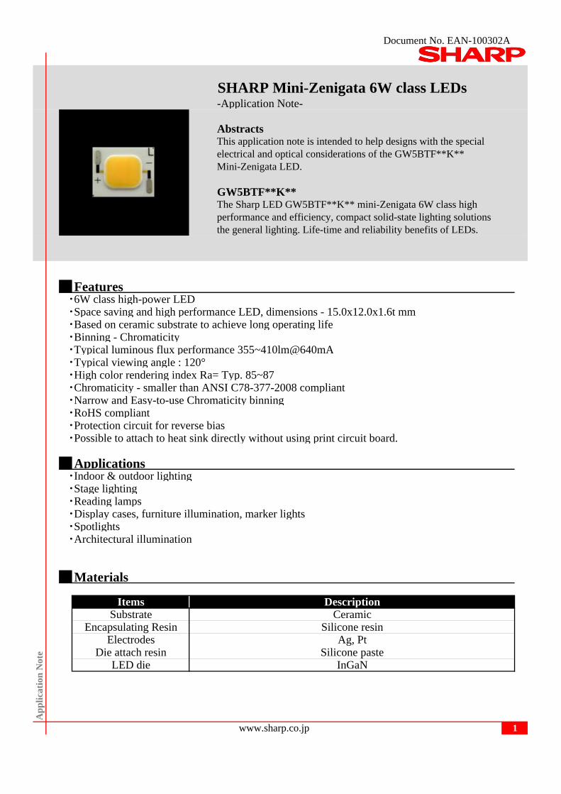
SHARP Mini-Zenigata 6W class LEDs-Application Note-
AbstractsThis application note is intended to help designs with the specialelectrical and optical considerations of the GW5BTF**K**Mini-Zenigata LED.
GW5BTF**K**The Sharp LED GW5BTF**K** mini-Zenigata 6W class highperformance and efficiency, compact solid-state lighting solutionsthe general lighting. Life-time and reliability benefits of LEDs.
Features ・6W class high-power LED ・Space saving and high performance LED, dimensions - 15.0x12.0x1.6t mm ・Based on ceramic substrate to achieve long operating life ・Binning - Chromaticity ・Typical luminous flux performance 355~410lm@640mA ・Typical viewing angle : 120° ・High color rendering index Ra= Typ. 85~87 ・Chromaticity - smaller than ANSI C78-377-2008 compliant ・Narrow and Easy-to-use Chromaticity binning ・RoHS compliant ・Protection circuit for reverse bias ・Possible to attach to heat sink directly without using print circuit board.
Applications ・Indoor & outdoor lighting ・Stage lighting ・Reading lamps ・Display cases, furniture illumination, marker lights ・Spotlights ・Architectural illumination
Materials
LED die
CeramicSilicone resin
Ag, PtSilicone paste
InGaN
Ap
pli
cati
on N
ote
www.sharp.co.jp 1
Items DescriptionSubstrate
Encapsulating ResinElectrodes
Die attach resin
Document No. EAN-100302A
GW5BTF**K**
Contents
Products lineup …
Absolute maximum ratings …
Chromaticity binning …
Emission spectrum …
Temperature characteristics …
Derating curves …
Electrical characteristics …
Reliability test data …
Flux distribution characteristics …
Appearance …
Protection circuit function …
Thermal resistance …
Heat design …
Handling …
How to mounting …
Instruction …
Optics …
Revision record …
2
Table of contents
Page
3
4
Ap
pli
cati
on N
ote
www.sharp.co.jp
5~10
38
23
11~16
17~22
24
25
26
27
28~29
30~32
33~36
37
44
39~40
41~43
Document No. EAN-100302A
GW5BTF**K**
Part No. definition
27 : CCT = 2700K Administration number30 : CCT = 3000K35 : CCT = 3500K40 : CCT = 4000K50 : CCT = 5000K65 : CCT = 6500K
The table describe the available colors and flux for GW5BTF**K** by correlated color temperatureby base part number. Note that the base order codes listed here are subset of the total available ordercodes for the product family. For more order codes, as well as a complete description of the order-code nomenclature, please consultthe GW5BTF**K** binning and labeling document.
83
81
85
87
87
87
87
85
GW5BTF35K00
CoolWhite
640mA 6020 7040 410 10.2 11.5 GW5BTF65K00
390 11.583NaturalWhite
640mA 3300 3600
11.5
K *
GW5BTF40KH0
10.2 GW5BTF30K00
Tc=25
GW5BTF50K0010.2
10.2
ColorDrive
currentCCT range
** *W 5 B
min.
T F
640mA 4745 5311
typ.
81
83
Products lineup
NaturalWhite
410
Forwardvoltage (V)
11.5390 10.2
min.
G
Ap
pli
cati
on N
ote
3www.sharp.co.jp
WarmWhite
640mA 2900 3150 375
GW5BTF27K00355
Part Numbertyp. max.max.
Flux (lm)
typ.
CRI
11.5
NaturalWhite
640mA 3900 4260 83
10.2 11.5WarmWhite
640mA 28002600
Document No. EAN-100302A
GW5BTF**K**
Absolute maximum ratings(for all GW5BTF**K** products family)
*1 Power dissipation and forward current are the value when the module temperatureis set lower than the rating by using an adequate heat sink.
*2 Voltage resistible at initial connection error(Not dealing with the possibility of always-on reverse voltage)
*3 Case temperature Tc (Refer to measuring point for case temperature in the page 33)
*4 Tc=25
Ap
pli
cati
on N
ote
4www.sharp.co.jp
Storage temperature
Absolute maximum ratings
Topr
Forward current *1,4 IF
Power dissipation *1,4 P
Parameter Symbol
Reverse voltage *2,4 VR
Operating temperature *3
Tstg
-30~+90
-40~+100
700
-15
mA
V
Unit
W
Rating
8.0

Document No. EAN-100302A
GW5BTF**K**
GW5BTF65K00 CCT=6500K Chromaticity binning
IF=640mA, Tc=25
Tolerance x,y ±0.01
12 0.3205 0.3481
0.3138 0.3238 0.3117 0.3393
Chromaticity Diagram
yRank
0.3217 0.33160.3058 0.3161
x y
5www.sharp.co.jp
Point 1 Point 2 Point 3 Point 4
0.3393 0.3138
y
Chromaticity binning
Ap
pli
cati
on N
ote
0.3238
x0.30280.3117
y x0.3304
x
0.30
0.32
0.34
0.36
0.38
0.40
0.42
0.44
0.30 0.32 0.34 0.36 0.38 0.40 0.42 0.44 0.46 0.48
x
y
12
Document No. EAN-100302A
GW5BTF**K**
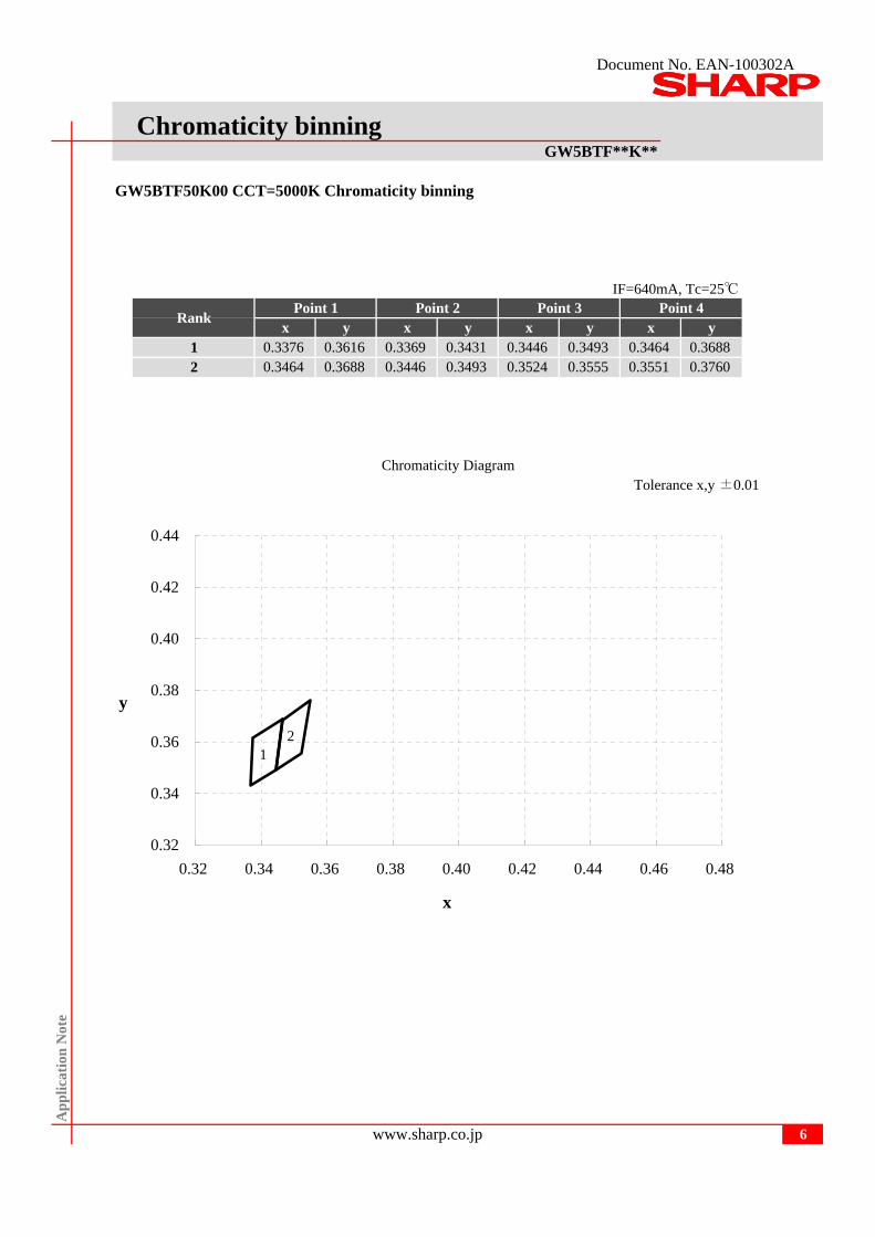
GW5BTF50K00 CCT=5000K Chromaticity binning
IF=640mA, Tc=25
Chromaticity binning
Ap
pli
cati
on N
ote
0.3493
x0.33760.3464
y x0.3616
x
6www.sharp.co.jp
Point 1 Point 2 Point 3 Point 4
0.3688 0.3446
y yRank
0.3524 0.35550.3369 0.3431
x y
Tolerance x,y ±0.01
12 0.3551 0.3760
0.3446 0.3493 0.3464 0.3688
Chromaticity Diagram
0.32
0.34
0.36
0.38
0.40
0.42
0.44
0.32 0.34 0.36 0.38 0.40 0.42 0.44 0.46 0.48
x
y
12
Document No. EAN-100302A
GW5BTF**K**
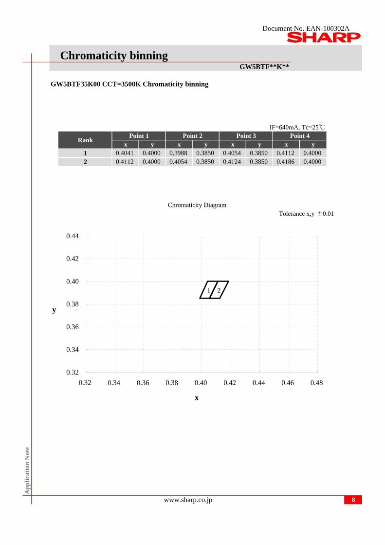
GW5BTF35K00 CCT=3500K Chromaticity binning
IF=640mA, Tc=25
Chromaticity binning
Ap
pli
cati
on N
ote
0.3850
x0.40410.4112
y x0.4000
x
8www.sharp.co.jp
Point 1 Point 2 Point 3 Point 4
0.4000 0.4054
y yRank
0.4124 0.38500.3988 0.3850
x y
Tolerance x,y ±0.01
12 0.4186 0.4000
0.4054 0.3850 0.4112 0.4000
Chromaticity Diagram
0.32
0.34
0.36
0.38
0.40
0.42
0.44
0.32 0.34 0.36 0.38 0.40 0.42 0.44 0.46 0.48
x
y
1 2
Document No. EAN-100302A
GW5BTF**K**
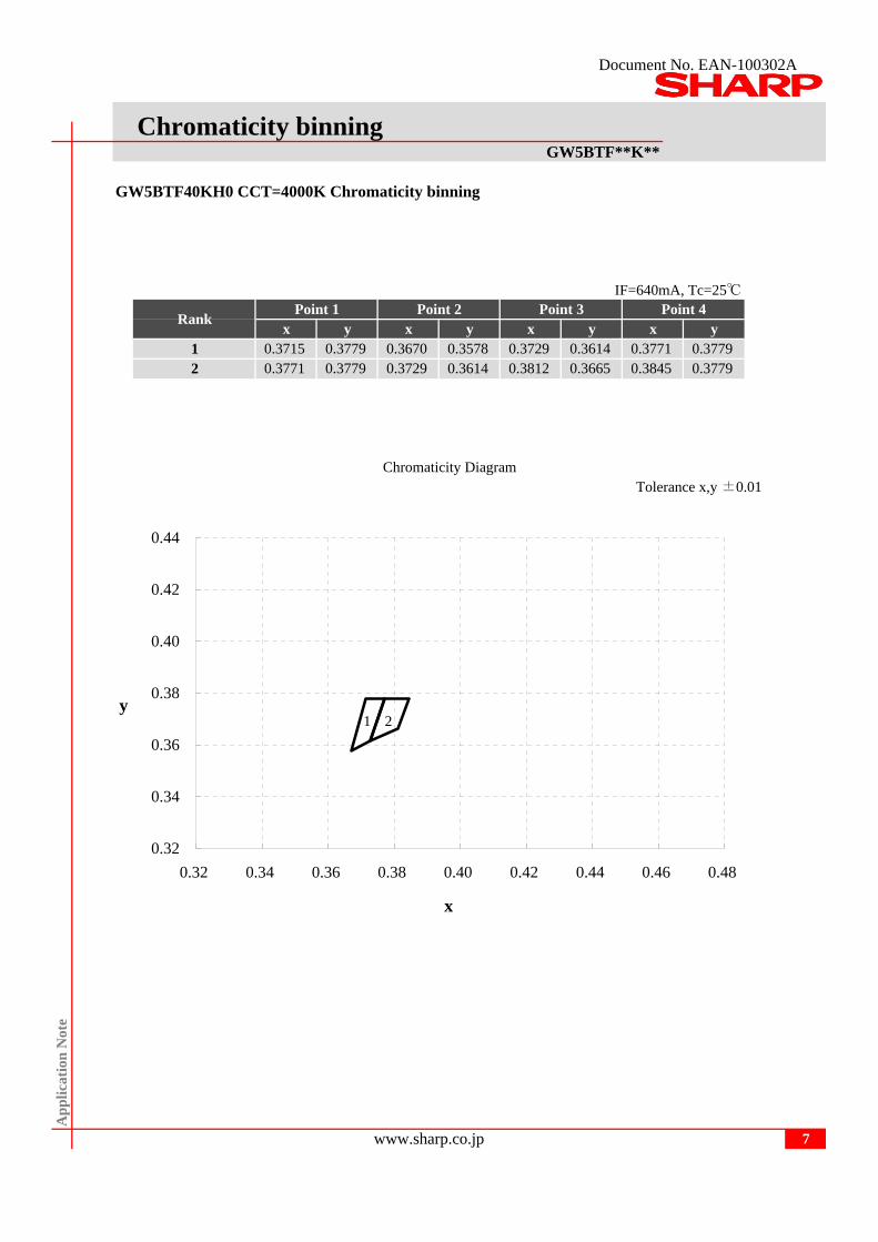
GW5BTF40KH0 CCT=4000K Chromaticity binning
IF=640mA, Tc=25
Tolerance x,y ±0.01
12 0.3845 0.3779
0.3729 0.3614 0.3771 0.3779
Chromaticity Diagram
yRank
0.3812 0.36650.3670 0.3578
x y
7www.sharp.co.jp
Point 1 Point 2 Point 3 Point 4
0.3779 0.3729
y
Chromaticity binning
Ap
pli
cati
on N
ote
0.3614
x0.37150.3771
y x0.3779
x
0.32
0.34
0.36
0.38
0.40
0.42
0.44
0.32 0.34 0.36 0.38 0.40 0.42 0.44 0.46 0.48
x
y1 2
Document No. EAN-100302A
GW5BTF**K**
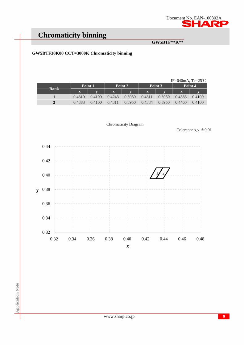
GW5BTF30K00 CCT=3000K Chromaticity binning
IF=640mA, Tc=25
Ap
pli
cati
on N
ote
Chromaticity Diagram
12 0.4460 0.4100
0.4243 0.3950 0.4100
Tolerance x,y ±0.01
Rank
0.4384 0.3950
x0.3950 0.4383
x y
9www.sharp.co.jp
Point 1 Point 2 Point 3 Point 4
0.4100 0.4311
y
Chromaticity binning
0.3950
x0.43100.4383
y x y0.4100 0.4311
0.32
0.34
0.36
0.38
0.40
0.42
0.44
0.32 0.34 0.36 0.38 0.40 0.42 0.44 0.46 0.48
x
y
1 2
Document No. EAN-100302A
GW5BTF**K**
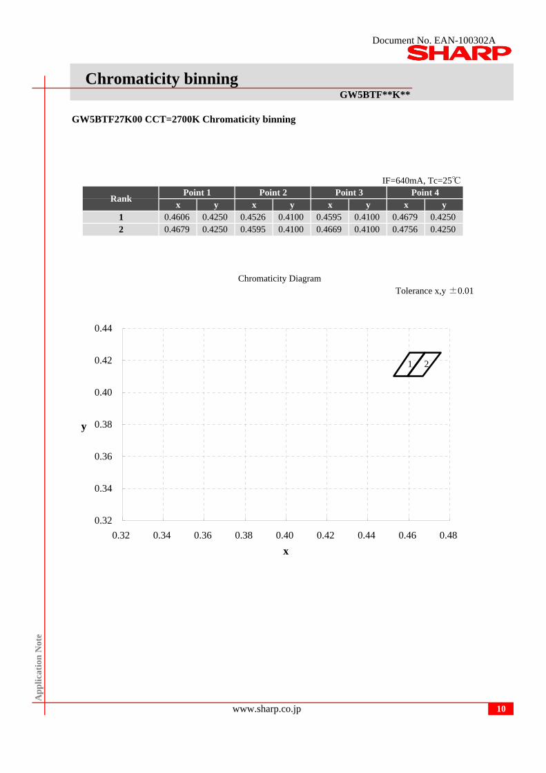
GW5BTF27K00 CCT=2700K Chromaticity binning
IF=640mA, Tc=25
Chromaticity binning
0.4100
x0.46060.4679
y x y0.4250 0.4595
10www.sharp.co.jp
Point 1 Point 2 Point 3 Point 4
0.4250 0.4595
yRank
0.4669 0.4100
x0.4100 0.4679
x y
Ap
pli
cati
on N
ote
Tolerance x,y ±0.01
12 0.4756 0.4250
0.4526 0.4100 0.4250
Chromaticity Diagram
0.32
0.34
0.36
0.38
0.40
0.42
0.44
0.32 0.34 0.36 0.38 0.40 0.42 0.44 0.46 0.48
x
y
1 2
Document No. EAN-100302A
GW5BTF**K**
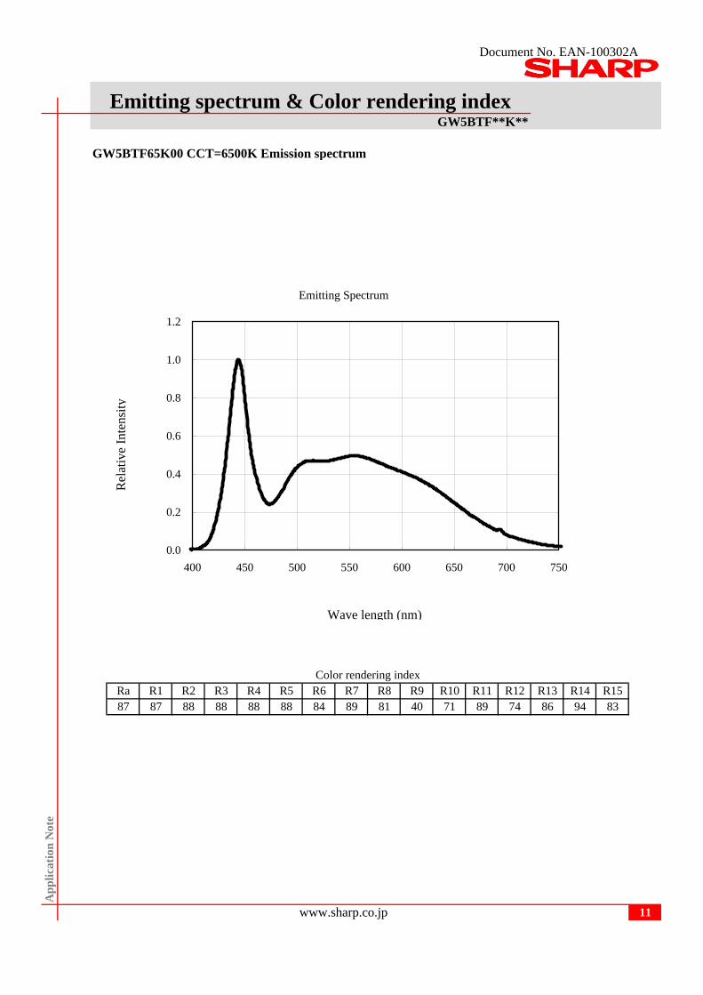
GW5BTF65K00 CCT=6500K Emission spectrum
Emitting spectrum & Color rendering index
Ap
pli
cati
on N
ote
11www.sharp.co.jp
R10 R11 R12Color rendering index
Emitting Spectrum
Ra87 87 88
R1 R288 88 88 84 8689 81 40 71
R8 R989 74
R158394
R3 R4 R13 R14R5 R6 R7
Wave length (nm)
Rel
ativ
e In
tens
ity
0.0
0.2
0.4
0.6
0.8
1.0
1.2
400 450 500 550 600 650 700 750

Document No. EAN-100302A
GW5BTF**K**
GW5BTF50K00 CCT=5000K Emission spectrum
Emitting spectrum & Color rendering index
Ap
pli
cati
on N
ote
12www.sharp.co.jp
R8 R9 R10Color rendering index
Emitting Spectrum
Ra R1 R2 R3 R4 R5 R6 R7 R11 R12 R13 R14 R1586 86 88 90 88 87 85 89 79 86 94 8240 73 89 75
Wave length (nm)
Rel
ativ
e In
tens
ity
0.0
0.2
0.4
0.6
0.8
1.0
1.2
400 450 500 550 600 650 700 750

Document No. EAN-100302A
GW5BTF**K**
GW5BTF40KH0 CCT=4000K Emission spectrum
Emitting spectrum & Color rendering index
Ap
pli
cati
on N
ote
13www.sharp.co.jp
R8 R9 R10
Emitting Spectrum
Color rendering indexRa R1 R2 R3 R4 R5 R6 R7 R11 R12 R13 R14 R1588 88 90 92 88 88 87 89 78 88 95 8443 77 90 79
Wave length (nm)
Rel
ativ
e In
tens
ity
0.0
0.2
0.4
0.6
0.8
1.0
1.2
400 450 500 550 600 650 700 750

Document No. EAN-100302A
GW5BTF**K**
GW5BTF35K00 CCT=3500K Emission spectrum
Emitting spectrum & Color rendering index
Ap
pli
cati
on N
ote
14www.sharp.co.jp
R8 R9 R10Color rendering index
Emitting Spectrum
Ra R1 R2 R3 R4 R5 R6 R7 R11 R12 R13 R14 R1588 87 91 95 89 87 89 90 75 87 97 8238 80 89 79
Rel
ativ
e In
tens
ity
Wave length (nm)
0.0
0.2
0.4
0.6
0.8
1.0
1.2
400 450 500 550 600 650 700 750
Document No. EAN-100302A
GW5BTF**K**
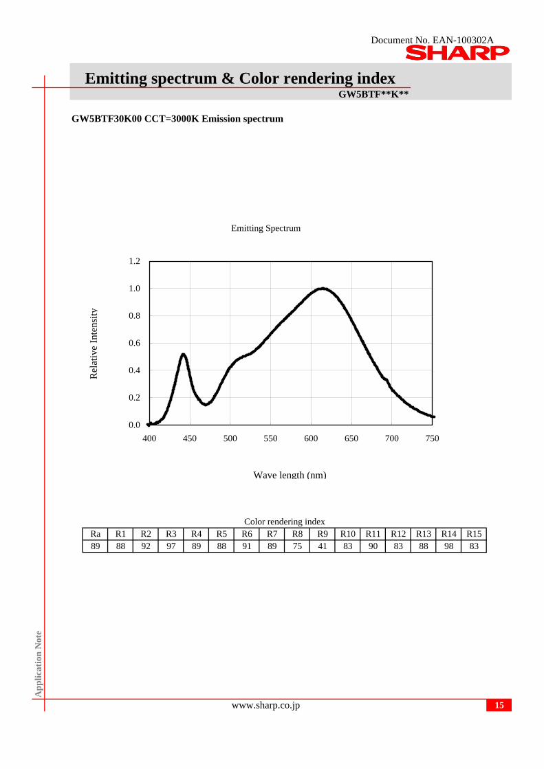
GW5BTF30K00 CCT=3000K Emission spectrum
Emitting spectrum & Color rendering index
Ap
pli
cati
on N
ote
15www.sharp.co.jp
R8 R9 R10Color rendering index
Emitting Spectrum
Ra R1 R2 R3 R4 R5 R6 R7 R11 R12 R13 R14 R1589 88 92 97 89 88 91 89 75 88 98 8341 83 90 83
Wave length (nm)
Rel
ativ
e In
tens
ity
0.0
0.2
0.4
0.6
0.8
1.0
1.2
400 450 500 550 600 650 700 750
Document No. EAN-100302A
GW5BTF**K**
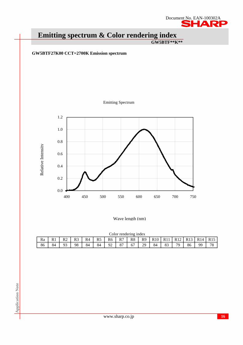
GW5BTF27K00 CCT=2700K Emission spectrum
Emitting spectrum & Color rendering index
Ap
pli
cati
on N
ote
16www.sharp.co.jp
R8 R9 R10Color rendering index
Emitting Spectrum
Ra R1 R2 R3 R4 R5 R6 R7 R11 R12 R13 R14 R1586 84 93 98 84 84 92 87 67 86 99 7829 84 83 79
Wave length (nm)
Rel
ativ
e In
tens
ity
0.0
0.2
0.4
0.6
0.8
1.0
1.2
400 450 500 550 600 650 700 750
Document No. EAN-100302A
GW5BTF**K**
GW5BTF65K00 CCT=6500K
Temperature characteristics
Ap
pli
cati
on N
ote
17www.sharp.co.jp
Chromaticity Coordinate vs. Case Temperature
IF = 640mA
Case Temperature vs Relative Luminous Flux
0
20
40
60
80
100
120
0 10 20 30 40 50 60 70 80 90
Case Temperature Tc []
Rel
ativ
e L
umin
ous
Flu
x [
%]
IF = 640 mA
0.310
0.320
0.330
0.340
0.300 0.310 0.320 0.330
x
y
0
25
90
60
40

Document No. EAN-100302A
GW5BTF**K**
GW5BTF50K00 CCT=5000K
Temperature characteristics
Ap
pli
cati
on N
ote
18www.sharp.co.jp
Case Temperature vs Relative Luminous Flux
0
20
40
60
80
100
120
0 10 20 30 40 50 60 70 80 90
Case Temperature Tc []
Rel
ativ
e L
umin
ous
Flu
x [
%]
IF = 640 mA
Chromaticity Coordinate vs. Case Temperature
IF = 640mA
0.340
0.350
0.360
0.370
0.330 0.340 0.350 0.360x
y
0
25
90
60
40

Document No. EAN-100302A
GW5BTF**K**
GW5BTF40KH0 CCT=4000K
Temperature characteristics
Ap
pli
cati
on N
ote
19www.sharp.co.jp
Chromaticity Coordinate vs. Case Temperature
IF = 640mA
Case Temperature vs Relative Luminous Flux
0
20
40
60
80
100
120
0 10 20 30 40 50 60 70 80 90
Case Temperature Tc []
Rel
ativ
e L
umin
ous
Flu
x [
%]
IF = 640 mA
0.350
0.360
0.370
0.380
0.360 0.370 0.380 0.390
x
y
0
25
90
60

Document No. EAN-100302A
GW5BTF**K**
GW5BTF35K00 CCT=3500K
Temperature characteristics
Ap
pli
cati
on N
ote
20www.sharp.co.jp
Chromaticity Coordinate vs. Case Temperature
IF = 640mA
Case Temperature vs Relative Luminous Flux
0
20
40
60
80
100
120
0 10 20 30 40 50 60 70 80 90
Case Temperature Tc []
Rel
ativ
e L
umin
ous
Flu
x [
%]
IF = 640 mA
0.370
0.380
0.390
0.400
0.390 0.400 0.410 0.420x
y
0
25
60
90

Document No. EAN-100302A
GW5BTF**K**
GW5BTF30K00 CCT=3000K
Temperature characteristics
Ap
pli
cati
on N
ote
21www.sharp.co.jp
Chromaticity Coordinate vs. Case Temperature
IF = 640mA
Case Temperature vs Relative Luminous Flux
0
20
40
60
80
100
120
0 10 20 30 40 50 60 70 80 90
Case Temperature Tc []
Rel
ativ
e L
umin
ous
Flu
x [
%]
IF = 640 mA
0.390
0.400
0.410
0.420
0.420 0.430 0.440 0.450x
y
0
25
40
90
60
Document No. EAN-100302A
GW5BTF**K**
GW5BTF27K00 CCT=2700K
Temperature characteristics
Ap
pli
cati
on N
ote
22www.sharp.co.jp
Chromaticity Coordinate vs. Case Temperature
IF = 640mA
Case Temperature vs Relative Luminous Flux
0
20
40
60
80
100
120
0 10 20 30 40 50 60 70 80 90
Case Temperature Tc []
Rel
ativ
e L
umin
ous
Flu
x [
%]
IF = 640 mA
0.400
0.410
0.420
0.430
0.450 0.460 0.470 0.480x
y
0
25
60
90
Document No. EAN-100302A
GW5BTF**K**
Derating Curves characteristics
To keep Tc (Case-temperature) lower than the rating enough heat-radiation performanceneeds to be secured by using an adequate heat sink.
Derating curves
Ap
pli
cati
on N
ote
23www.sharp.co.jp
<Fig.1> Forward Current Derating Curve
0
100
200
300
400
500
600
700
800
-30 -20 -10 0 10 20 30 40 50 60 70 80 90 100
Case Temperature Tc []
For
war
d C
urre
nt I
F [
mA
]
Document No. EAN-100302A
GW5BTF**K**
Electrical Characteristics
Electrical characteristics
Ap
pli
cati
on N
ote
24www.sharp.co.jp
<Fig.3> Forward Voltage vs Forward Current
0
100
200
300
400
500
600
700
800
7.0 8.0 9.0 10.0 11.0Forward Voltage [V]
For
war
d C
urre
nt [
mA
]
Tc = 25
<Fig.2> Forward Current vs Reliability Luminous Flux
0
20
40
60
80
100
120
0 100 200 300 400 500 600 700 800
Forward Current IF [mA]
Rel
ativ
e L
umin
ous
Flu
x [%
]
Tc = 25
Document No. EAN-100302A
GW5BTF**K**
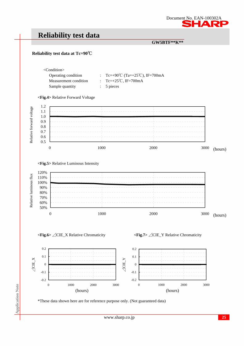
Reliability test data at Tc=90
<Condition>Operating condition : Tc=+90 (Ta=+25), IF=700mAMeasurement condition : Tc=+25, IF=700mASample quantity : 5 pieces
<Fig.4> Relative Forward Voltage
<Fig.5> Relative Luminous Intensity
<Fig.6> ⊿CIE_X Relative Chromaticity <Fig.7> ⊿CIE_Y Relative Chromaticity
*These data shown here are for reference purpose only. (Not guaranteed data)
Reliability test data
Ap
pli
cati
on N
ote
25www.sharp.co.jp
(hours)
Rel
ativ
e fo
rwar
d vo
ltag
eR
elat
ive
lum
inou
s fl
ux⊿
CIE
_X
⊿C
IE_Y
(hours)
(hours) (hours)
-0.2
-0.1
0
0.1
0.2
0 1000 2000 3000
-0.2
-0.1
0
0.1
0.2
0 1000 2000 3000
50%60%70%80%90%
100%110%120%
0 1000 2000 3000
0.50.60.70.80.91.01.11.2
0 1000 2000 3000
Document No. EAN-100302A
GW5BTF**K**
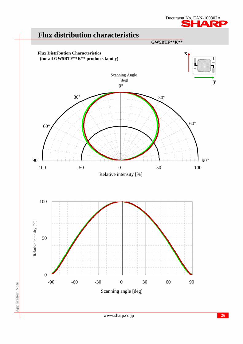
Flux Distribution Characteristics x (for all GW5BTF**K** products family)
Flux distribution characteristics
Ap
pli
cati
on N
ote
26www.sharp.co.jp
y
90°
60°
30°
0°
30°
60°
90°
-100 -50 0 50 100Relative intensity [%]
Scanning Angle[deg]
0
50
100
-90 -60 -30 0 30 60 90
Scanning angle [deg]
Rel
ativ
e in
tens
ity [
%]
Document No. EAN-100302A
GW5BTF**K**
Appearance
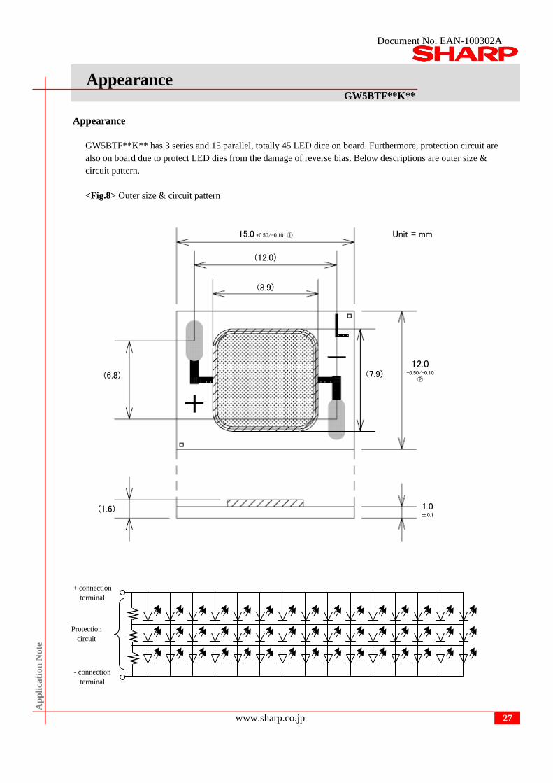
GW5BTF**K** has 3 series and 15 parallel, totally 45 LED dice on board. Furthermore, protection circuit arealso on board due to protect LED dies from the damage of reverse bias. Below descriptions are outer size & circuit pattern.
<Fig.8> Outer size & circuit pattern
Appearance
Ap
pli
cati
on N
ote
27www.sharp.co.jp
+ connectionterminal
- connectionterminal
Protectioncircuit
1.0±0.1
15.0 +0.50/-0.10 ①
12.0+0.50/-0.10
②
Unit = mm
(8.9)
(7.9)
(12.0)
(6.8)
(1.6)
Document No. EAN-100302A
GW5BTF**K**
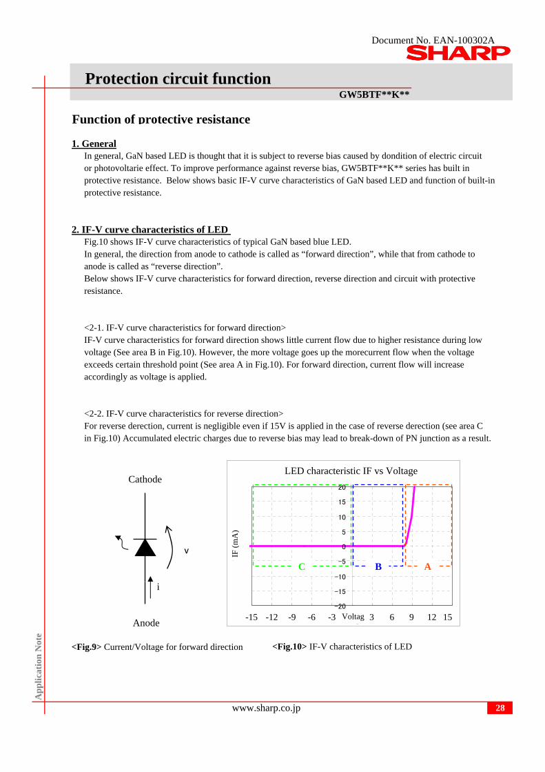
Function of protective resistance
1. GeneralIn general, GaN based LED is thought that it is subject to reverse bias caused by dondition of electric circuitor photovoltarie effect. To improve performance against reverse bias, GW5BTF**K** series has built inprotective resistance. Below shows basic IF-V curve characteristics of GaN based LED and function of built-inprotective resistance.
2. IF-V curve characteristics of LED Fig.10 shows IF-V curve characteristics of typical GaN based blue LED.In general, the direction from anode to cathode is called as “forward direction”, while that from cathode toanode is called as “reverse direction”. Below shows IF-V curve characteristics for forward direction, reverse direction and circuit with protective resistance.
<2-1. IF-V curve characteristics for forward direction>IF-V curve characteristics for forward direction shows little current flow due to higher resistance during lowvoltage (See area B in Fig.10). However, the more voltage goes up the morecurrent flow when the voltageexceeds certain threshold point (See area A in Fig.10). For forward direction, current flow will increaseaccordingly as voltage is applied.
<2-2. IF-V curve characteristics for reverse direction>For reverse derection, current is negligible even if 15V is applied in the case of reverse derection (see area Cin Fig.10) Accumulated electric charges due to reverse bias may lead to break-down of PN junction as a result.
<Fig.9> Current/Voltage for forward direction
Protection circuit function
Ap
pli
cati
on N
ote
28www.sharp.co.jp
<Fig.10> IF-V characteristics of LED
Cathode
Anode
i
v
LEDの電流-電圧特性
-20
-15
-10
-5
0
5
10
15
20
-5 -4 -3 -2 -1 0 1 2 3 4 5電圧(V)
電流
(m
A)
C
LED characteristic IF vs Voltage
voltage
IF (
mA
)
AB
-15 -9 96-3-12 -6 3 12Voltag 15

Document No. EAN-100302A
GW5BTF**K**
<2-3. Protective Resistor Function>Fig.12 shows IF-V curve characteristics for a LED with built-in protective resistor. During low voltage in the case of forward direction with over threshold voltage, current goes through not resisterbut LED.On the other hand, current flow to protective resistor will become dominant in case reverse direction voltage isapplied because reverse current of LED is negligible. 15V in case of reverse direction. So protection circuit hasby-pass function for reverse bias.
<Fig.11> Diagram for LED <Fig.12> IF-V Characteristics for LED & protective resistor & protective resistor
<2-4. Current flow to protective resistor>Mini-zenigata LED should be used in adequate forward current to bring out required luminouce performance.Expected range of current, Mini-zenigata LED is designed as a lmost all current drive through LED. Fig.13shows approximate current to resister by operation current as a reference value.
<Fig.13> Input Current vs. Current loaded in protective resistor
Current flow to protective resistor at over 100mA of input current is approx. 0.001mA (1μA).1/100,000 level of current flow in LED. Impact of protective resistor to power consumption will be negligible.
GW5BTF**K** series incorporates protection circuit for reverse direction, which is supposed tofunction against temporary reverse voltage. This protection circuit will not work for a product for which reverse voltage is loaded constantly.
200240
Input Current(mA)
<1.0
<1.0<1.0<1.0<1.0
Protection circuit function
Ap
pli
cati
on N
ote
29www.sharp.co.jp
400
100
Approx. current value(μA)
150
Cathode
Anode
i1 i2
V
LED+Protection circuit vs Voltage
-1000
-500
0
500
1000
-5 -4 -3 -2 -1 0 1 2 3 4 5
IF(n A
)
LED only
LED protective resistance
Protective resistance only
-15 -9 96-3-12 -6 3 12 15Voltag
Document No. EAN-100302A
GW5BTF**K**
1 .GeneralAlong with the improvement of luminous efficiency, LED is getting widely used these days forapplications which require high output power such as LED lighting and backlight system for LCD TV.The more prevail, the more input power is required for LED and the more heat is generateddramatically. When LED device generates heat, it will cause degradation of luminous efficiency and life,which will result in difficulty in obtaining expected performance. It is essential, therefore, that optimumheat. Here is the explanation of resistance necessary for heat design and how the temperature goes upin the actual usage conditions.
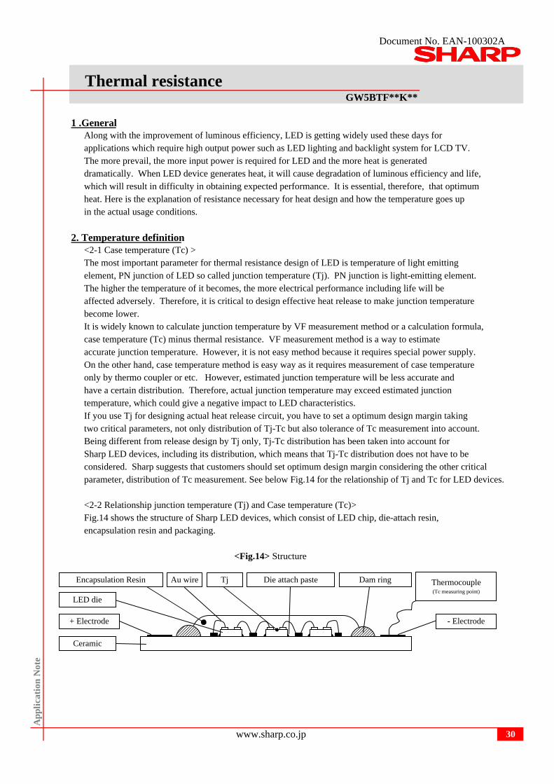
2. Temperature definition<2-1 Case temperature (Tc) >The most important parameter for thermal resistance design of LED is temperature of light emittingelement, PN junction of LED so called junction temperature (Tj). PN junction is light-emitting element.The higher the temperature of it becomes, the more electrical performance including life will beaffected adversely. Therefore, it is critical to design effective heat release to make junction temperaturebecome lower.It is widely known to calculate junction temperature by VF measurement method or a calculation formula,case temperature (Tc) minus thermal resistance. VF measurement method is a way to estimateaccurate junction temperature. However, it is not easy method because it requires special power supply.On the other hand, case temperature method is easy way as it requires measurement of case temperatureonly by thermo coupler or etc. However, estimated junction temperature will be less accurate andhave a certain distribution. Therefore, actual junction temperature may exceed estimated junctiontemperature, which could give a negative impact to LED characteristics.If you use Tj for designing actual heat release circuit, you have to set a optimum design margin takingtwo critical parameters, not only distribution of Tj-Tc but also tolerance of Tc measurement into account. Being different from release design by Tj only, Tj-Tc distribution has been taken into account forSharp LED devices, including its distribution, which means that Tj-Tc distribution does not have to beconsidered. Sharp suggests that customers should set optimum design margin considering the other criticalparameter, distribution of Tc measurement. See below Fig.14 for the relationship of Tj and Tc for LED devices.
<2-2 Relationship junction temperature (Tj) and Case temperature (Tc)>Fig.14 shows the structure of Sharp LED devices, which consist of LED chip, die-attach resin,encapsulation resin and packaging.
<Fig.14> Structure
Thermal resistance
App
lica
tion
Not
e
30www.sharp.co.jp
Au wire Dam ring
Ceramic
- Electrode
Encapsulation Resin Thermocouple(Tc measuring point)
Tj
+ Electrode
Die attach paste
LED die
Document No. EAN-100302A
GW5BTF**K**
Heat release path from location of heat generation for LED chip to LED terminal is as follows;
When Sharp LED is actually used, it is mounted on a print circuit board by soldering with heat sink whennecessary. In this case, heat release path will be as follows;
Heat release path can be written by using a factor called thermal resistance as shown in the electricaldiagram Fig.15.
<Fig.15> Thermal diagram with thermal resistance
Tj: Junction Temperature Rjc: Thermal resistance between junction and caseTc: Case Temperature Rch: Thermal resistance between case and heat sink Th: Heat sink temperature Rha: Thermal resistance between heat sink and ambientTa: Ambient Temperature Rca: Thermal resistance between case and ambient
Rja: Thermal resistance between junction and ambient
<Fig.16> Pattern diagram of temperature slope
Tjc: Temperature difference in Tj and TcTch: Temperature difference in Tc and Th
Tha: Temperature difference between Th and Ta
Thermal resistance
Ap
pli
cati
on N
ote
31www.sharp.co.jp
LED chip --> Die-attach resin (Resin for attach LED to substrate) --> Ceramic substrate --> LED terminal
LED chip --> Die-attach resin --> Ceramic substrate --> LED terminal --> print circuit board --> heat sink
LED die
Die attach resinCeramic substrate
Terminal Printed Circuit Board &Heat sink
Ambient
Adhesive etcTj Tc Th Ta
Rjc Rch Rha
Rja
Rca
Tj
Tc
Th
Ta
Temperature slope represents thermal resistance.The slower the slope is, the better heat release performance is.
Input Power
Temperature raise
Tha
Tch
Tjc
It is fundamental to relax the slope of Tc-Ta curvefor better heat release performance.
Document No. EAN-100302A
GW5BTF**K**
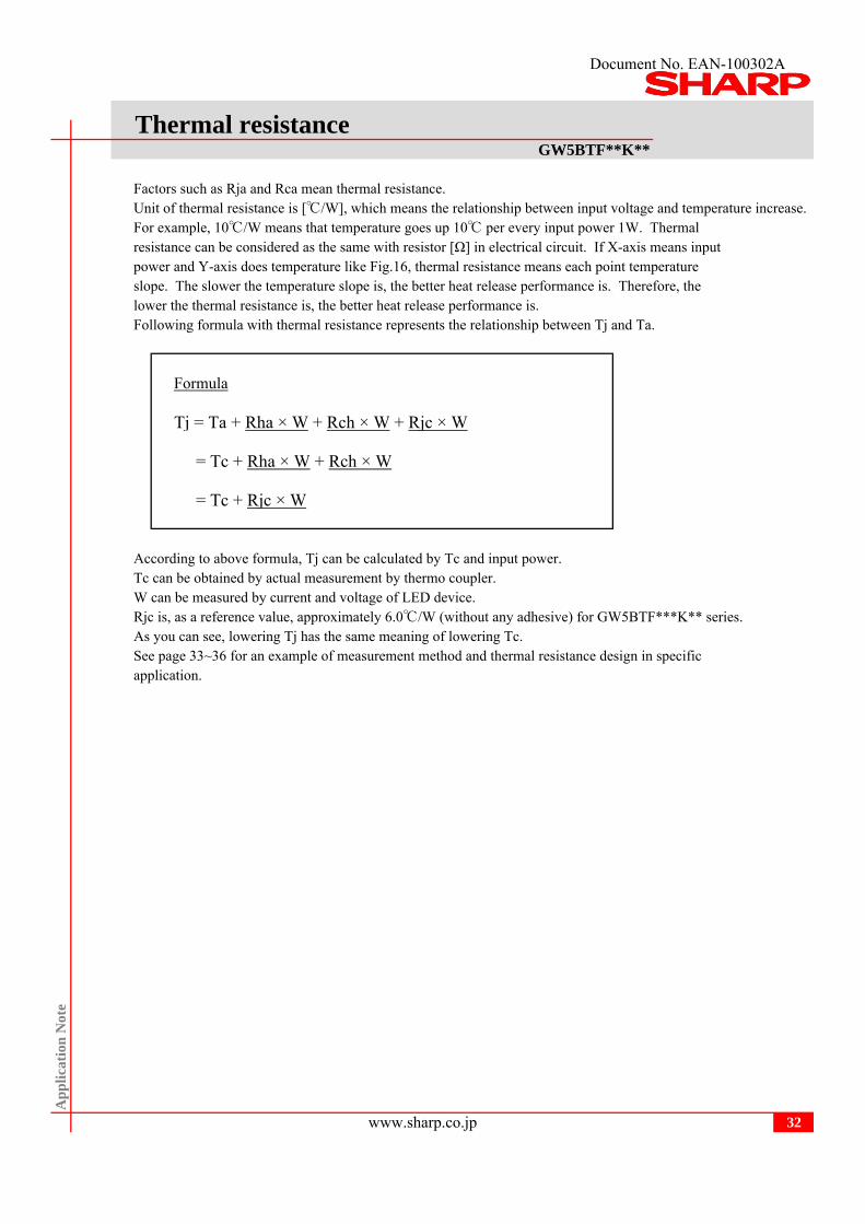
Factors such as Rja and Rca mean thermal resistance.Unit of thermal resistance is [/W], which means the relationship between input voltage and temperature increase.For example, 10/W means that temperature goes up 10 per every input power 1W. Thermalresistance can be considered as the same with resistor [Ω] in electrical circuit. If X-axis means input power and Y-axis does temperature like Fig.16, thermal resistance means each point temperatureslope. The slower the temperature slope is, the better heat release performance is. Therefore, thelower the thermal resistance is, the better heat release performance is.Following formula with thermal resistance represents the relationship between Tj and Ta.
Formula
Tj = Ta + Rha × W + Rch × W + Rjc × W
= Tc + Rha × W + Rch × W
= Tc + Rjc × W
According to above formula, Tj can be calculated by Tc and input power.Tc can be obtained by actual measurement by thermo coupler.W can be measured by current and voltage of LED device. Rjc is, as a reference value, approximately 6.0/W (without any adhesive) for GW5BTF***K** series.As you can see, lowering Tj has the same meaning of lowering Tc.See page 33~36 for an example of measurement method and thermal resistance design in specificapplication.
Thermal resistance
Ap
pli
cati
on N
ote
32www.sharp.co.jp
Document No. EAN-100302A
GW5BTF**K**
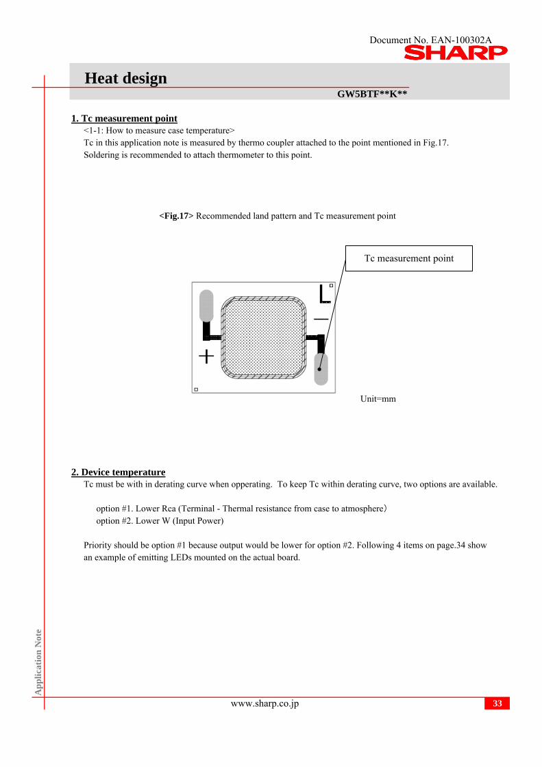
1. Tc measurement point<1-1: How to measure case temperature>Tc in this application note is measured by thermo coupler attached to the point mentioned in Fig.17.Soldering is recommended to attach thermometer to this point.
<Fig.17> Recommended land pattern and Tc measurement point
Unit=mm
2. Device temperatureTc must be with in derating curve when opperating. To keep Tc within derating curve, two options are available.
option #1. Lower Rca (Terminal - Thermal resistance from case to atmosphere)option #2. Lower W (Input Power)
Priority should be option #1 because output would be lower for option #2. Following 4 items on page.34 showan example of emitting LEDs mounted on the actual board.
Heat design
Ap
pli
cati
on N
ote
33www.sharp.co.jp
Tc measurement point
Document No. EAN-100302A
GW5BTF**K**
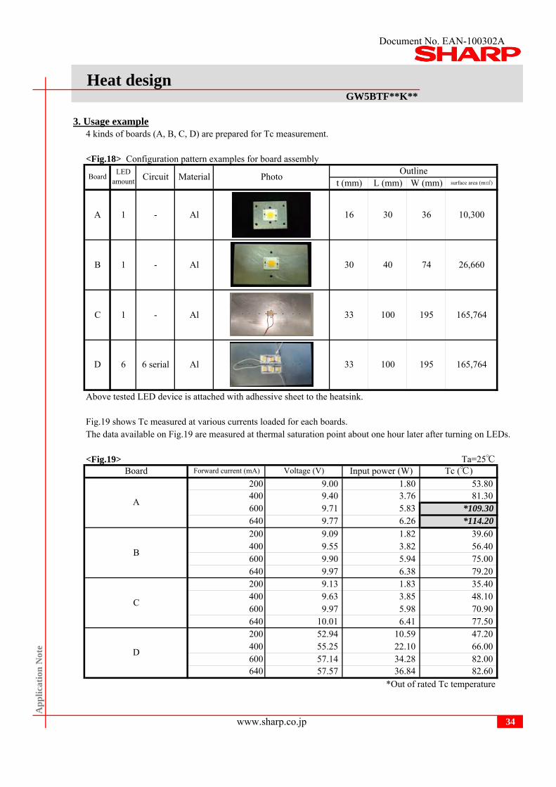
3. Usage example4 kinds of boards (A, B, C, D) are prepared for Tc measurement.
<Fig.18> Configuration pattern examples for board assembly
Above tested LED device is attached with adhessive sheet to the heatsink.
Fig.19 shows Tc measured at various currents loaded for each boards. The data available on Fig.19 are measured at thermal saturation point about one hour later after turning on LEDs.
<Fig.19> Ta=25
165,764
195
surface area (m)
10,300
26,660
165,764
OutlineW (mm)
16
30
t (mm) L (mm)
30 36
40 74B
LEDamount
-
-
1
1
Circuit
Heat design
Ap
pli
cati
on N
ote
34www.sharp.co.jp
D
33
Al
1
6
-
6 serial
Board
C Al
Photo
Forward current (mA)
Material
Al
Al
Board
A
A
100
640 9.77 6.26
200 9.00 1.80400
100
9.40 3.76
33
Voltage (V)
195
Input power (W)
9.09 1.82
B
6.38640 9.97
600 9.71 5.83
600 9.90 5.94400 9.55 3.82200
200 9.13 1.83
200 52.94
600 9.97400 9.63 3.85
640
10.59
57.57 36.8434.28600 57.14
400 55.25 22.10
640 10.01 6.415.98 70.90
79.20
Tc ()53.8081.30
*109.30*114.20
39.6056.4075.00
*Out of rated Tc temperature
C
D
82.60
77.5047.2066.0082.00
35.4048.10
Document No. EAN-100302A
GW5BTF**K**
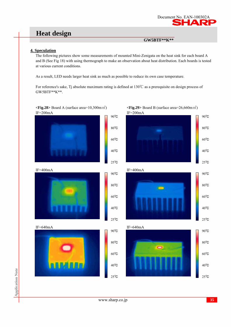
4. SpeculationThe following pictures show some measurements of mounted Mini-Zenigata on the heat sink for each board Aand B (See Fig 18) with using thermograph to make an observation about heat distribution. Each boards is testedat various current conditions.
As a result, LED needs larger heat sink as much as possible to reduce its own case temperature.
For reference's sake, Tj absolute maximum rating is defined at 130 as a prerequisite on design process ofGW5BTF**K**.
<Fig.28> Board A (surface area=10,300m) <Fig.29> Board B (surface area=26,660m)IF=200mA IF=200mA
IF=400mA IF=400mA
IF=640mA IF=640mA
Heat design
Ap
pli
cati
on N
ote
www.sharp.co.jp 35
60
25
40
80
90
60
25
40
80
90
60
25
40
80
90
60
25
40
80
90
60
25
40
80
90
60
25
40
80
90
Document No. EAN-100302A
GW5BTF**K**
6. Design flow chart
if NOT, go back toprocedure No.1and reconsider.
Use in the singular (*a) Use in the plural (*b)
measuring
monitor
-When measuring Tc, measured LED should be built on to the lighting fixture module.
measuring monitor -Chose the measured LED device which assumed the highest Tc in the mounted LEDs.
Heat design
Ap
pli
cati
on N
ote
36www.sharp.co.jp
5. Implemented above condition *Possible to use as it stands.
1. Mounting LED(s) on the board.
2. Built-in 2-1. Building on to the lighting fixture module. 2-2. Setting on the actual using condition.
3. How to measure Tc 3-1. With using thermo couple. (*a,*b) 3-2. Chose the measured LED device which assumed the highest Tc in the mounted LEDs. (*b) 3-3. Under stable temperature condition.
4. Judgment of Tc 4-1. Not over the temperature of your standard rated ? 4-2. Not over the temperature of specified on LED device specification sheet ? (See Fig.1)
5. NOT implemented *Reducing forward current *Reconsider its design of thermal resistance
LED
Board
xx
Thermo couple
LED
heat sink / board
xx
Document No. EAN-100302A
GW5BTF**K**
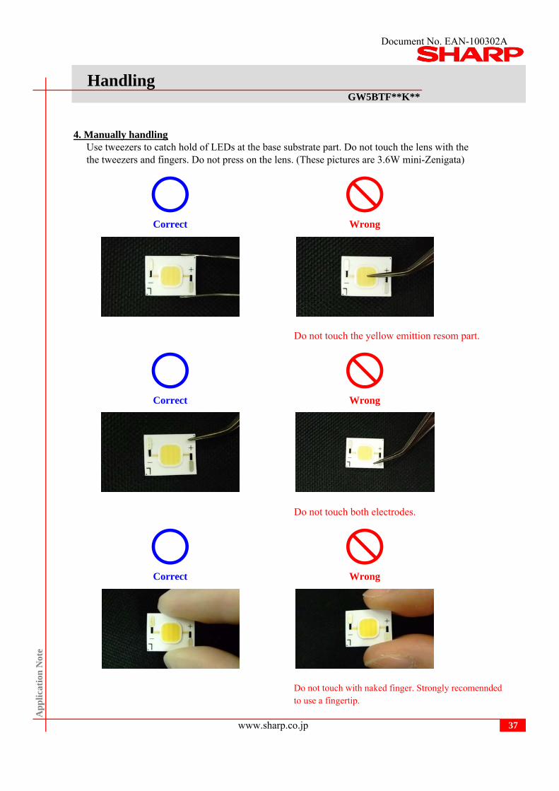
4. Manually handlingUse tweezers to catch hold of LEDs at the base substrate part. Do not touch the lens with thethe tweezers and fingers. Do not press on the lens. (These pictures are 3.6W mini-Zenigata)
Do not touch the yellow emittion resom part.
Do not touch both electrodes.
Do not touch with naked finger. Strongly recomenndedto use a fingertip.
Ap
pli
cati
on N
ote
Handling
37www.sharp.co.jp
WrongCorrect
WrongCorrect
Correct Wrong
Document No. EAN-100302A
GW5BTF**K**
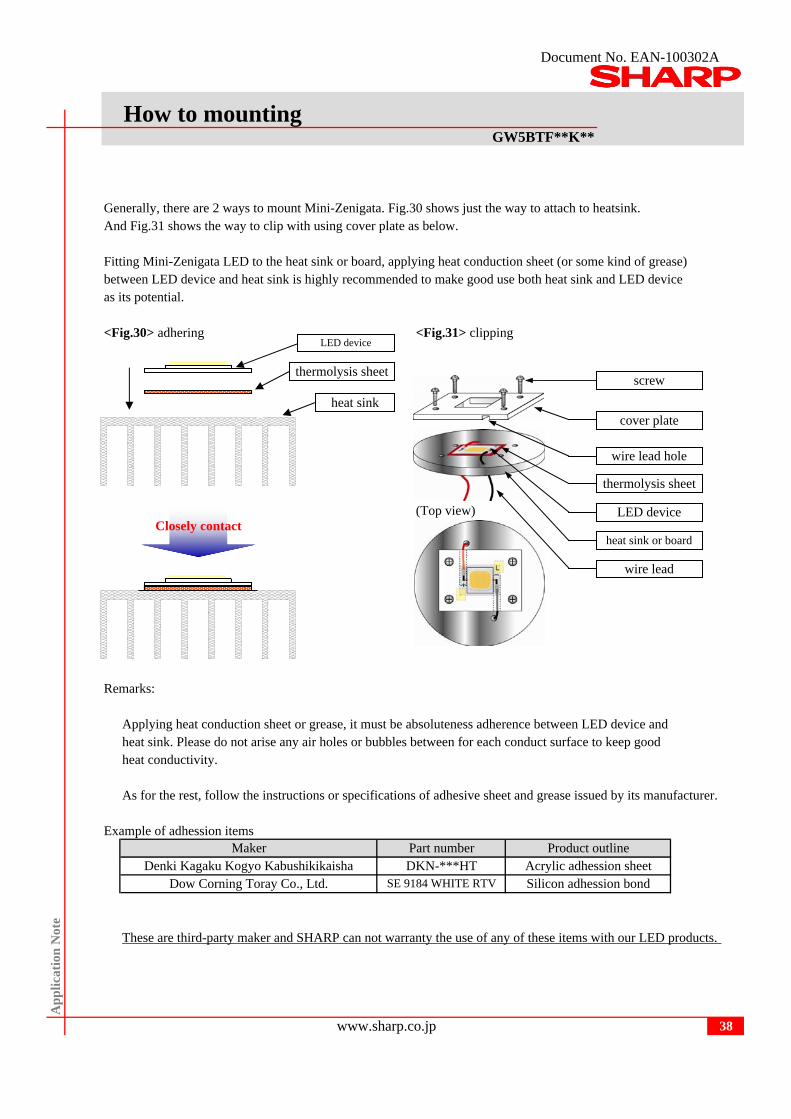
Generally, there are 2 ways to mount Mini-Zenigata. Fig.30 shows just the way to attach to heatsink.And Fig.31 shows the way to clip with using cover plate as below.
Fitting Mini-Zenigata LED to the heat sink or board, applying heat conduction sheet (or some kind of grease)between LED device and heat sink is highly recommended to make good use both heat sink and LED device as its potential.
<Fig.30> adhering <Fig.31> clipping
(Top view)
Remarks:
Applying heat conduction sheet or grease, it must be absoluteness adherence between LED device andheat sink. Please do not arise any air holes or bubbles between for each conduct surface to keep goodheat conductivity.
As for the rest, follow the instructions or specifications of adhesive sheet and grease issued by its manufacturer.
Example of adhession items
These are third-party maker and SHARP can not warranty the use of any of these items with our LED products.
How to mounting
Ap
pli
cati
on N
ote
www.sharp.co.jp 38
Dow Corning Toray Co., Ltd. SE 9184 WHITE RTV Silicon adhession bond
Maker Part number Product outlineDenki Kagaku Kogyo Kabushikikaisha DKN-***HT Acrylic adhession sheet
screw
cover plate
wire lead hole
thermolysis sheet
LED device
heat sink or board
wire lead
LED device
heat sink
thermolysis sheet
Closely contact
Document No. EAN-100302A
GW5BTF**K**
1 Storage conditionsPlease follow the conditions below.・Before opened: Temperature 5 ~ 30 , Relative humidity less than 60 %. (Before opened LED should be used within a year)・After opened: Temperature 5 ~ 30 , Relative humidity less than 60 %. (Please apply soldering within 1 week)・After opened LED should be kept in an aluminum moisture proof bag with a moisture absorbent material (silica gel).・Avoid exposing to air with corrosive gas.If exposed, electrode surface would be damaged, which may affect soldering.
2 Usage conditionsThe products are not designed for the use under any of the following conditions.Please confirm their performance and reliability well enough if you use under any of the following conditions;・In a place with a lot of moisture, dew condensation, briny air, and corrosive gas. (Cl, H2S, NH3, SO2, NOX, etc.)・Under the direct sunlight, outdoor exposure, and in a dusty place.・In water, oil, medical fluid, and organic solvent.
3 Heat radiationIf the forward current (IF) is applied to single-state module at any current, there is a risk of damaging module
or emitting smoke.Equip with specified heat radiator, and avoid heat stuffed inside the module.
4 InstallationMaterial of board is alumina ceramic. If installed inappropriately, trouble of no radiation may occur due toboard crack or overheat. Please take particular notice for installing method.Further information on installation, refer to the following cautions.・ Apply thermolysis adhesive, adhesive sheet or peculiar connector when mounted on heat radiator.
In case of applying adhesive or adhesive sheet only, check the effectiveness and reliability before fixing.If LED comes off from the heat radiator, unusual temperature rise entails hazardous phenomena including device deterioration, coming off of solder at leads, and emitting smoke.
・ When LED device is mechanically fixed or locked, Please take it into consideration regarding method of attach due to fail from stress.
・ Avoid convexly uneven boards.Those convex boards are subject to substrate cracking or debasement of heat release.
・ It is recommended to apply adhesive or adhesive sheet with high thermal conductivityto radiate heat effectively.
・ Please take care about the influence of color change of adhesive or adhesive sheet in initial and long termperiod, which may affect light output or color due to change of reflectance from backside.
5 Module surface strength Module surface is subject to mechanical stress. Applying stress to surface of modules results in damage on resin and internal failure. Please do not pressurize on the part of resin.
Instruction
Ap
pli
cati
on N
ote
39www.sharp.co.jp

Document No. EAN-100302A
GW5BTF**K**
6 Connecting method In case of solder connecting method, follow the conditions mentioned below.・Use Soldering iron with thermo controller (tip temperature 380 ), within 5 seconds per one place.・Secure the solder wettability on whole solder pad and leads.・During the soldering process, put the ceramic board on materials whose conductivity is poor enough not to radiate heat of soldering.・Warm up (with using a heated plate) the substrate is recommended before soldering.・Avoid touching a part of resin with soldering iron.・This product is not designed for reflow and flow soldering.・Avoid such lead arrangement as applying stress to solder-applied area.・Please do not detach solder and make re-solder.・Please solder evenly on each electrodes.・Please prevent flux from touching to resin.
7 Static electricity This product is subject to static electricity, so take measures to cope with it. Install circuit protection device to drive circuit, if necessary.
8 Drive method・Any reverse voltage cannot be applied to LEDs when they are in operation or not. Design a circuit so that any flow of reverse or forward voltage can not be applied to LEDs when they are out of operation.・Module is composed of LEDs connected in both series and parallel. Constant voltage power supply runs off more than specified current amount due to lowered VF
caused by temperature rise. Constant current power supply is recommended to drive.
9 Cleaning Avoid cleaning, since silicone resin is eroded by cleaning.
10 Color-tone variation Chromaticity of this product is monitored by integrating sphere right after the operation. Chromaticity varies depending on measuring method, light spread condition, or ambient temperature. Please verify your actual conditions before use.
11 Safety・Looking directly at LEDs for a long time may result in hurt your eyes.・In case that excess current (over ratings) are supplied to the device, hazardous phenomena including abnormal heat generation, emitting smoke, or catching fire can be caused. Take appropriate measures to excess current and voltage.・In case of solder connecting method, there is a possibility of fatigue failure by heat. Please fix the leads in such case to protect from short circuit or leakage of electricity caused by contact.・Please confirm the safety standards or regulations of application devices.・Please careful not to injure your hand by edge of ceramic substrate.
12 The formal specification must be exchanged before beginning your mass production.
Instruction
Ap
pli
cati
on N
ote
40www.sharp.co.jp
Document No. EAN-100302A
GW5BTF**K**
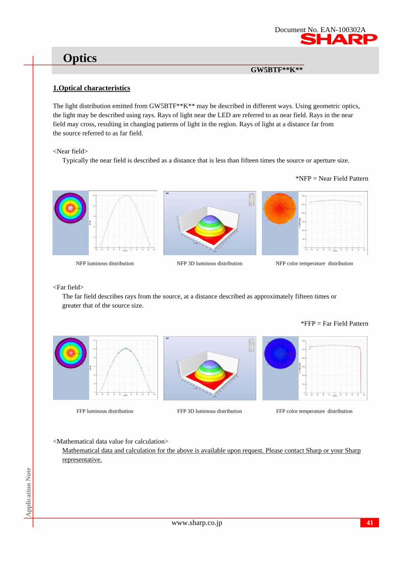
1.Optical characteristics
The light distribution emitted from GW5BTF**K** may be described in different ways. Using geometric optics,the light may be described using rays. Rays of light near the LED are referred to as near field. Rays in the near field may cross, resulting in changing patterns of light in the region. Rays of light at a distance far from the source referred to as far field.
<Near field>Typically the near field is described as a distance that is less than fifteen times the source or aperture size.
*NFP = Near Field Pattern
<Far field>The far field describes rays from the source, at a distance described as approximately fifteen times or greater that of the source size.
*FFP = Far Field Pattern
<Mathematical data value for calculation>Mathematical data and calculation for the above is available upon request. Please contact Sharp or your Sharprepresentative.
Ap
pli
cati
on N
ote
Optics
41www.sharp.co.jp
NFP luminous distribution NFP 3D luminous distribution NFP color temperature distribution
FFP luminous distribution FFP 3D luminous distribution FFP color temperature distribution

Document No. EAN-100302A
GW5BTF**K**
2.Optics tool
The following makers' lenses for LEDs may help in your optical design.
Several makers' lens & reflector produce optics that work well with GW5BTF**K** arrays to enable rapid systemdesign. Here are some off-the-shelf products that can be used with GW5BTF**K**.These are third-party optics and SHARP can not warranty the use of any of these optics with our LED products. Please check with the supplier for the latest information about product specification and more details from their URL.
address: Via Molinetto, 40Zip: 36075 Montecchio MaggioreCountry: ItalyTel: +39 444 800 547Fax: +39 444 800 548e-mail: [email protected]: http://www.idealed.it/
address: Tehdaskatu 13Zip: 24100 SALOCountry: FinlandTel: +358 40 833 83 83Fax: +358 2 733 8001e-mail: [email protected]: http://www.ledil.fi/
For information about LEDIL reflector products for GW5BTF**K**, please see this URLhttp://www.ledil.fi/index.php?page=mini_zenigata
Ap
pli
cati
on N
ote
Optics
42www.sharp.co.jp
Type No: 35mm conic lens
Type No: Candy MZEN C10982 Type No: Candy MZEN C10983 Type No: Candy MZEN C10984
Document No. EAN-100302A
GW5BTF**K**
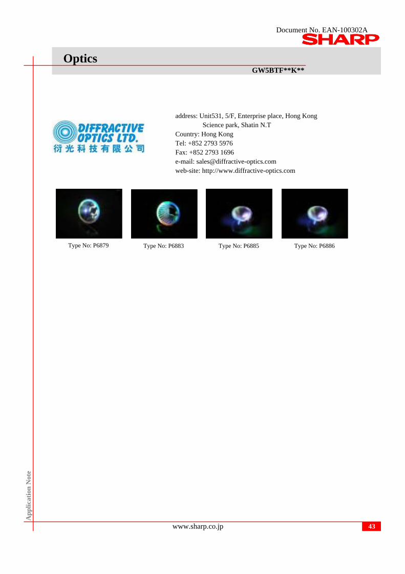
address: Unit531, 5/F, Enterprise place, Hong Kong Science park, Shatin N.TCountry: Hong KongTel: +852 2793 5976Fax: +852 2793 1696e-mail: [email protected]: http://www.diffractive-optics.com
Ap
pli
cati
on N
ote
Optics
43www.sharp.co.jp
Type No: P6879 Type No: P6883 Type No: P6885 Type No: P6886

Document No. EAN-100302A
GW5BTF**K**
Ap
pli
cati
on N
ote
Revision record
44www.sharp.co.jp
Date Doc. Number Page ContentsApr-19 2010 EAN-100302 First edition
Apr-27 2010 EAN-100302A 1 <Modification> Amendment of product name from "Mini-Zenigata 6.7W" to "Mini-Zenigata
6W class".


